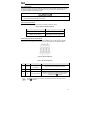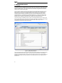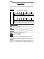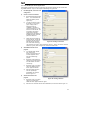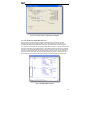
1
ICC
Instruction Manual
INDUSTRIAL CONTROL COMMUNICATIONS, INC.
OPC-E1-WiE
Multiprotocol Wireless
Ethernet Interface
Thank you for purchasing the OPC-E1-WiE Multiprotocol Wireless Ethernet Interface.
•
This product is designed to connect the FRENIC-Multi series of inverters to wireless Ethernet
communication networks. Please read this instruction manual thoroughly in order to become
familiar with the proper interface handling, installation and usage procedures.
•
Improper handling may inhibit correct operation or cause premature interface failure.
•
Please deliver this instruction manual to the end user of the interface, and retain it in an
accessible location.
•
For inverter usage instructions, please refer to the applicable FRENIC-Multi inverter instruction
manual.
May 2009
ICC #10719-1.000-000
© 2009 Industrial Control Communications, Inc.
ICC
OPC-E1-WiE Multiprotocol Wireless Ethernet Interface Instruction Manual
Part Number 10719-1.000-000
Printed in U.S.A.
©2009 Industrial Control Communications, Inc.
All rights reserved
Industrial Control Communications, Inc. reserves the right to make changes and improvements to its
products without providing notice.
Notice to Users
INDUSTRIAL CONTROL COMMUNICATIONS, INC.’S PRODUCTS ARE NOT AUTHORIZED FOR USE
AS CRITICAL COMPONENTS IN LIFE-SUPPORT DEVICES OR SYSTEMS. Life-support devices or
systems are devices or systems intended to sustain life, and whose failure to perform, when properly
used in accordance with instructions for use provided in the labeling and user's manual, can be
reasonably expected to result in significant injury.
No complex software or hardware system is perfect. Bugs may always be present in a system of any
size. In order to prevent danger to life or property, it is the responsibility of the system designer to
incorporate redundant protective mechanisms appropriate to the risk involved.
1
ICC
Preface
Thank you for purchasing the OPC-E1-WiE Multiprotocol Wireless Ethernet Interface. This instruction
manual has been prepared to help you connect your FRENIC-Multi inverter to a variety of wireless
Ethernet control networks.
This instruction manual does not contain inverter usage instructions. Please refer to this instruction
manual in conjunction with the FRENIC-Multi Instruction Manual (INR-SI47-1094-E) in order to become
familiar with the proper handling, installation and operation of this product. Improper handling or
installation procedures may result in incorrect operation or premature product failure.
Please keep this instruction manual in a safe place.
Related Publications
Listed below are publications that are recommended for reference in conjunction with this instruction
manual.
• RS-485 Communication User's Manual ........... (MEH448)
• FRENIC-Multi Instruction Manual .................... (INR-SI47-1094-E)
These documents are subject to change without notice. Please be sure to refer to the most recent
available versions.
Safety precautions
Please read this instruction manual thoroughly prior to proceeding with installation, connections,
operation, or maintenance and inspection. Additionally, ensure that all aspects of the system are fully
understood, and familiarize yourself with all safety information and precautions before operating the
inverter.
Safety precautions in this instruction manual are classified into the following two categories:
Failure to heed the information indicated by this symbol may lead
to dangerous conditions, possibly resulting in death or serious
bodily injuries.
Failure to heed the information indicated by this symbol may lead
to dangerous conditions, possibly resulting in minor or light bodily
injuries and/or substantial property damage.
Failure to heed the information contained under the CAUTION title can also result in serious
consequences. These safety precautions are of utmost importance and must be observed at all times.
2
ICC
Installation and wiring
•
To avoid electrical shock, remove all power from the inverter and wait at least five minutes prior to
starting installation. Additionally, confirm that the DC link bus voltage as measured between the
P (+) and N (-) terminals is less than 25 VDC.
•
Installation should be performed only by qualified personnel.
•
To avoid electrical shock, do not operate the inverter with the front cover or wiring cover removed,
as accidental contact with exposed high-voltage terminals and internal components may occur.
•
To prevent explosions or similar damage, ensure that all cables are properly connected to the
correct terminals, and observe all wiring polarity indicators.
•
Do not install or operate the interface if it is damaged or has parts missing.
•
Prevent conductive items such as screws and metal fragments, or flammable substances such as
oil, lint, paper fibers and sawdust from entering the inverter and interface card enclosure.
•
Incorrect handling during installation or removal may cause equipment failure.
•
Do not subject the cables to scratches, excessive stress, heavy loads or pinching.
•
To prevent damage due to electrostatic discharge, always touch a grounded piece of metal prior
to touching any equipment.
•
Do not stand on or rest heavy objects on the equipment.
•
To prevent burns from hot components, do not touch the inverter while power is on, or for some
time after power is removed.
•
Electrical noise may be emitted from the inverter, motor and wires. Always implement
appropriate countermeasures to prevent nearby sensors and devices from malfunctioning due to
such noise.
Operation
•
To avoid electrical shock, do not open the front cover of the inverter while power is on or while the
inverter is running.
•
To avoid electrical shock, do not operate switches with wet hands.
•
If the inverter’s function codes are incorrectly configured, or configured without adequate
understanding of the FRENIC-Multi Instruction Manual (INR-SI47-1094-E) and FRENIC-Multi
User's Manual (MEH457), the motor may rotate with a torque or at a speed not permitted for the
machine. Confirm the settings of all function codes prior to running the inverter.
3
ICC
Maintenance, inspection, and parts replacement
•
To avoid electrical shock, remove all power from the inverter and wait at least five minutes prior to
starting inspection. Additionally, confirm that the DC link bus voltage as measured between the P
(+) and N (-) terminals is less than 25 VDC.
•
Maintenance, inspection, and parts replacement should be performed only by qualified personnel.
•
Remove all watches, rings and other metallic objects prior to starting work.
•
To avoid electrical shock or other injuries, always use insulated tools.
Disposal
•
Contact the local or state environmental agency in your area for details on the disposal of
electrical components and packaging.
Other
•
Do not attempt to modify the equipment: doing so may cause electrical shock or injuries.
•
For clarity purposes, illustrations in this manual may be drawn with covers or safety guards
removed. Ensure all covers and safety guards are properly installed prior to starting operation.
•
Do not perform hi-pot tests on the equipment.
•
Performing a data initialization (function code H03) may reset all inverter function codes to their
factory default settings. After performing this operation, remember to reenter any custom function
code values prior to starting operation.
Icons
The following icons are used throughout this manual:
Indicates information which, if not heeded, can result in the product not operating to full
efficiency, as well as information concerning incorrect operations and settings which may
result in accidents.
Indicates information that can prove handy when performing certain settings or operations.
Indicates a reference to more detailed information.
4
ICC
− TABLE OF CONTENTS −
1
PRE-OPERATION INSTRUCTIONS............................................................. 8
1.1
Product Overview....................................................................................................8
1.2
Unpacking and Product Confirmation ................................................................10
1.2.1
1.2.2
1.3
LED Indicators .......................................................................................................12
1.3.1
1.3.2
1.4
2
4
INSTALLATION .......................................................................................... 14
2.1
Pre-Installation Instructions.................................................................................14
2.2
Installation Procedure ..........................................................................................15
2.3
Power Supply ........................................................................................................18
2.4
Antenna Options ...................................................................................................19
Initial Wireless Settings ........................................................................................21
2.6
Resetting the Wireless Settings to Factory Defaults.........................................21
INVERTER FUNCTION CODE SETTINGS ................................................ 22
3.1
RS-485 Communication Settings.........................................................................22
3.2
Inverter Control-Related Settings........................................................................24
FINDER APPLICATION.............................................................................. 25
4.1
Overview ................................................................................................................25
4.2
Configuring the IP Address..................................................................................26
Via the Finder Utility......................................................................................................... 26
Via the Web Page ............................................................................................................ 26
EMBEDDED WEB SERVER....................................................................... 27
5.1
Overview ................................................................................................................27
5.2
Authentication .......................................................................................................28
5.3
Page Select Tabs...................................................................................................28
5.4
Monitor Tab............................................................................................................28
5.4.1
5.4.2
5.4.3
5.4.4
5.4.5
5.4.6
Information Window ......................................................................................................... 28
Function Code Group Selection List................................................................................. 29
Function Code List ........................................................................................................... 29
Function Code List Filter .................................................................................................. 30
Non-Scanned Function Code Refresh.............................................................................. 31
Radix Selection ................................................................................................................ 31
5.5
Profinet Tab ...........................................................................................................31
5.6
BACnet Tab............................................................................................................32
5.6.1
5.6.2
5
Standard Dipole Antenna ................................................................................................. 19
Optional #10694 Antenna Extension Cable...................................................................... 20
Optional #10693 Desktop/Magnetic Antenna ................................................................... 20
2.5
4.2.1
4.2.2
5
Module Status and Network Status LEDs ........................................................................ 12
Wireless Ethernet Link and Activity LEDs ........................................................................ 12
Environmental Specifications ..............................................................................13
2.4.1
2.4.2
2.4.3
3
Shipment Confirmation..................................................................................................... 10
Component Overview....................................................................................................... 11
Information Window ......................................................................................................... 32
Device Identifiers ............................................................................................................. 32
ICC
5.6.3
5.7
5.7.1
5.7.2
5.7.3
5.7.4
5.7.5
5.7.6
5.7.7
5.8
Information Window ......................................................................................................... 34
Authentication Configuration ............................................................................................ 34
IP Address Configuration ................................................................................................. 35
MAC Address Configuration............................................................................................. 35
Wireless Settings ............................................................................................................. 35
Timeout Configuration...................................................................................................... 36
Submitting Changes......................................................................................................... 37
EtherNet/IP Tab .....................................................................................................38
5.8.1
5.8.2
5.8.3
5.8.4
5.8.5
5.9
Submitting Changes......................................................................................................... 33
Config Tab..............................................................................................................34
Information Window ......................................................................................................... 38
Device Identification ......................................................................................................... 38
Run/Idle Flag Behavior..................................................................................................... 39
Class 1 (I/O) Data Configuration Arrays ........................................................................... 39
Submitting Changes......................................................................................................... 40
Alarm Tab...............................................................................................................41
5.9.1
5.9.2
5.9.3
5.9.4
Information Window ......................................................................................................... 41
Email Configuration.......................................................................................................... 42
Alarm Configuration ......................................................................................................... 43
Submitting Changes......................................................................................................... 44
5.10 Modbus Tab ...........................................................................................................45
5.10.1
5.10.2
5.10.3
5.10.4
Information Window ......................................................................................................... 45
Supervisory Timer Selection ............................................................................................ 45
Register Remap Configuration ......................................................................................... 46
Submitting Changes......................................................................................................... 47
5.11 Dashboard Tab ......................................................................................................48
5.11.1
5.11.2
5.11.3
5.11.4
5.11.5
6
7
8
Information Window ......................................................................................................... 48
Virtual Keypad.................................................................................................................. 49
Gauge Window Navigation............................................................................................... 50
Gauge Window Configuration .......................................................................................... 50
Submitting Changes......................................................................................................... 53
FUNCTION CODE NUMBERING AND BEHAVIOR................................... 54
6.1
Register Numbers .................................................................................................54
6.2
Scanned and Non-Scanned Registers ................................................................55
FILESYSTEM & FIRMWARE ..................................................................... 57
7.1
Overview ................................................................................................................57
7.2
Initiating FTP via the Finder Utility ......................................................................58
7.3
Using FTP with Windows Explorer......................................................................58
7.4
Using FTP with a Windows Command Prompt ..................................................60
7.5
Using FTP with Core FTP LE................................................................................61
7.6
Loading New Application Firmware ....................................................................62
PROTOCOL-SPECIFIC INFORMATION .................................................... 63
8.1
Modbus TCP ..........................................................................................................63
8.1.1
8.1.2
8.2
Overview.......................................................................................................................... 63
Coil & Discrete Input Mappings ........................................................................................ 64
EtherNet/IP .............................................................................................................65
8.2.1
8.2.2
Overview.......................................................................................................................... 65
ODVA AC/DC Drive Profile .............................................................................................. 65
6
ICC
8.2.3
8.2.4
8.2.5
8.2.6
8.2.7
8.2.8
8.2.9
8.3
Allen Bradley CSP .................................................................................................80
8.3.1
8.3.2
8.3.3
8.3.4
8.3.5
8.3.6
8.4
7
Overview.......................................................................................................................... 80
Tag Reference ................................................................................................................. 80
SLC-5/05 Example: Read a Register Block...................................................................... 82
SLC-5/05 Example: Read a Single Register..................................................................... 85
SLC-5/05 Example: Multiple MSG Instructions................................................................. 86
SLC-5/05 Example: Reading and Writing......................................................................... 87
BACnet/IP...............................................................................................................88
8.4.1
8.4.2
8.4.3
9
ControlLogix Examples: Setup ......................................................................................... 68
ControlLogix Example: I/O Messaging ............................................................................. 69
Explicit Messaging Tag Reference................................................................................... 72
ControlLogix Explicit Messaging Example: Read a Register Block................................... 73
ControlLogix Explicit Messaging Example: Read a Single Register ................................. 78
ControlLogix Explicit Messaging Example: Multiple MSG Instructions ............................. 78
ControlLogix Explicit Messaging Example: Reading and Writing...................................... 79
Protocol Implementation Conformance Statement ........................................................... 88
Supported Objects ........................................................................................................... 91
Supported Object Details ................................................................................................. 93
TROUBLESHOOTING................................................................................ 94
ICC
1
PRE-OPERATION INSTRUCTIONS
1.1 Product Overview
The OPC-E1-WiE wireless Ethernet multiprotocol communication interface allows information to be
transferred seamlessly between a FRENIC-Multi inverter and several different wireless Ethernet-based
fieldbus networks with minimal configuration requirements. The interface installs directly onto the
inverter, and presents a standard 802.11b wireless Ethernet (Wi-Fi) antenna port for connection to the
wireless network. In addition to the supported fieldbus protocols, the interface also hosts an embedded
web server, which provides access to inverter information via a standard web browser for remote
monitoring, configuration and control.
Before using the interface, please familiarize yourself with the product and be sure to thoroughly read
the instructions and precautions contained in this manual. In addition, please make sure that this
instruction manual is delivered to the end user of the interface, and keep this instruction manual in a safe
place for future reference or unit inspection.
Note that different interface firmware versions may provide varying levels of support for the various
protocols. When using this manual, therefore, always keep in mind that the firmware version running on
your interface must match this manual’s respective revision in order for all documented aspects to apply.
The primary features of the OPC-E1-WiE are as follows:
Wireless Ethernet
IEEE 802.11b wireless Ethernet compliant, operating in the 2.4GHz band with data rates up 11Mbit/s.
Supports multiple simultaneous protocols, and allows a variety of encryption options, such as WEP,
WPA and WPA2.
Supported Protocols
The interface currently provides server support for the following fieldbus protocols:
•
Modbus TCP
•
EtherNet/IP
•
Allen Bradley CSP (also known as “PCCC” and “AB Ethernet”)
•
BACnet/IP
Antenna Options
The interface includes a detachable 2.4GHz omni-directional fully articulating dipole antenna with RPTNC connector. The antenna can be rotated 360 degrees at its connection point and from 0 to 90
degrees at its knuckle. An optional desktop/magnetic base antenna (ICC part #10693) and 30cm
antenna extension cable (ICC part #10694) are also available. Refer to section 2.4.
Adobe® Flash-Enabled Embedded Web Server
Interface configuration and real-time inverter register monitoring & control are provided via an embedded
web server. The interface’s web server feature provides direct data access and control via standard
web browsers such as Microsoft Internet Explorer and Mozilla Firefox. The latest version of Adobe
Flash Player browser plug-in is required. Refer to section 5.
XML Configuration File Upload/Download
All interface configuration files are stored in the unit’s internal filesystem in XML format. These files can
be transferred to/from a PC via the FTP protocol, which provides the capability for PC-based file backup
and easy configuration copying to multiple units. Configuration files can also be viewed and edited via
standard text editors, XML editors and web browsers. Refer to section 7.
Email-Based Alarm Notifications
Up to 20 configurable alarm conditions can be programmed into the interface. Value, logical comparison
and time-based conditions can be provided for the interface to autonomously monitor any available
inverter register. When an alarm condition is triggered, a notification email can be sent to up to four
destination email addresses. Refer to section 5.9.
Dashboard GUI
A dashboard tab on the embedded web server provides 10 gauge windows, each of which can be
configured to display any available scanned inverter register in a variety of meter, graph and gauge
formats. A virtual keypad interface is also provided. Refer to section 5.11.
8
ICC
Network Timeout Action
A configurable network timeout action can be programmed that allows registers to have their own unique
"fail-safe" conditions in the event of a network interruption. Refer to section 5.7.6.
Field-Upgradeable
As new firmware becomes available, the interface can be upgraded in the field by the end-user. Refer to
section 7.6 for more information.
EtherNet/IP Data Access Options
The EtherNet/IP protocol provides access to inverter data via explicit messaging, user-defined I/O
assembly instances, and the ODVA AC/DC drive profile. Refer to section 8.2 for more information.
9
ICC
1.2 Unpacking and Product Confirmation
1.2.1 Shipment Confirmation
Check the enclosed items. Confirm that the correct quantity of each item was received, and that no
damage occurred during shipment.
•
•
•
2
OPC-E1-WiE interface board (with antenna) in enclosure (see Figure 1).
One option retaining screw (see Figure 2).
Two option connection cables (see Figure 3). The short cable is used for 3.7kW and smaller
inverters, and the long cable is used for 5.5kW and larger inverters.
Figure 2: Option Retaining Screw
Figure 1: OPC-E1-WiE Interface Board with Antenna
Figure 3: Option Connection Cables
10
ICC
1.2.2 Component Overview
Figure 4 shows an overview of the important interface card components. For clarity, the enclosure cover
has been removed.
RJ45 keypad connector
CN1
MAC ID
Power supply
terminal block
Network status LED
Module status LED
Antenna jack
Figure 4: OPC-E1-WiE Component Overview
Power Supply Terminal Block
The power supply terminal block can be used to provide power (7-24VDC) to the interface card. Refer
to section 2.3.
Network Status and Module Status LEDs
These LEDs indicate the current status of the interface card and protocols in use. Refer to section 1.3.1.
Antenna Module Housing with Embedded LEDs and MAC ID
The antenna is connected here, and the embedded LEDs provide insight into the wireless Ethernet
network’s status and activity. Refer to section 1.3.2. The unique MAC ID for the interface card is also
located on a barcode sticker on top of the antenna module housing.
Connector CN1
An option connection cable is plugged in here to allow the interface card to communicate to the inverter.
Refer to section 2.2.
RJ45 Keypad Connector
This is the connector used to connect the inverter’s keypad to the interface card.
11
The keypad can also be detached from the interface card and panel-mounted. For details,
refer to the FRENIC-Multi Instruction Manual (INR-SI47-1094-E), Chapter 2, Section 2.4
"Mounting and Connecting a Keypad."
ICC
1.3 LED Indicators
1.3.1 Module Status and Network Status LEDs
Two stacked LEDs near the antenna module housing provide a visual indication of the unit’s overall
status and communications activity. Refer to Figure 5.
1.3.2 Wireless Ethernet Link and Activity LEDs
The antenna module housing also contains two embedded LEDs that provide insight into the wireless
Ethernet network. Refer to Figure 5.
Network Status LED
• This LED conforms to the
prescribed “network status LED”
behavior as dictated in the EtherNet/IP
specification, Volume 2, Chapter 9.
Module Status LED
• This LED conforms to the
prescribed “module status LED”
behavior as dictated in the EtherNet/IP
specification, Volume 2, Chapter 9.
• Contact ICC technical support if a
blinking red error code is observed.
Ethernet Activity LED
This green LED blinks briefly
when network packets are
sent or received.
Link Integrity LED
This yellow LED:
• Is on solid whenever a connection
(link integrity) has been established
between the interface card and an
access point (infrastructure mode.)
• Blinks slowly whenever the
interface card in ad hoc mode.
• Blinks quickly whenever the
interface card is scanning for a
network.
Figure 5: LED Indicators
12
ICC
1.4 Environmental Specifications
The interface’s environmental specifications are detailed in Table 1.
Table 1: Environmental Specifications
Item
Specification
Operating Environment
Indoors, less than 1000m above sea level, do not expose to direct
sunlight or corrosive / explosive gasses
Operating Temperature
-10 ∼ +50°C (+14 ∼ +122°F)
Storage Temperature
-40 ∼ +85°C (-40 ∼ +185°F)
Relative Humidity
20% ∼ 90% (without condensation)
Vibration
5.9m/s2 (0.6G) or less (10 ∼ 55Hz)
Grounding
Referenced to incoming power supply
Power supply
7-24VDC
Cooling Method
Self-cooled
Communication Speed
Up to 11Mbps with automatic fallback
The OPC-E1-WiE interface is lead-free / RoHS-compliant.
13
ICC
2
INSTALLATION
2.1 Pre-Installation Instructions
•
To avoid electrical shock, remove all power from the inverter and wait at least five minutes prior to
starting installation. Additionally, confirm that the DC link bus voltage as measured between the
P (+) and N (-) terminals is less than 25 VDC.
•
Installation should be performed only by qualified personnel.
•
To avoid electrical shock, do not operate the inverter with the front cover or wiring cover removed,
as accidental contact with exposed high-voltage terminals and internal components may occur.
•
To prevent explosions or similar damage, ensure that all cables are properly connected to the
correct terminals, and observe all wiring polarity indicators.
14
ICC
2.2 Installation Procedure
Before installing the interface card, perform all wiring for the main circuit terminals and
control circuit terminals.
1.
Remove the terminal cover from the inverter.
Note: For inverters with a capacity of 5.5 to 15 kW, the terminal cover retaining screw must first
be removed in order to remove the terminal cover.
2.
3.
Insert an option connection cable into the CN1 connector on the inverter’s interface PCB. The
short cable is used for 3.7kW and smaller inverters, and the long cable is used for 5.5kW and
larger inverters.
Reinstall the terminal cover.
4.
For details on how to remove the terminal cover, refer to the FRENIC-Multi Instruction
Manual (INR-SI47-1094-E), Chapter 2, Section 2.3 "Wiring."
For details on how to reinstall the terminal cover, refer to the FRENIC-Multi Instruction
Manual (INR-SI47-1094-E), Chapter 2, Section 2.3 "Wiring."
Depress the latches provided on both sides of the keypad and pull the keypad up and off of the
inverter.
For details on how to remove the keypad, refer to the FRENIC-Multi Instruction Manual
(INR-SI47-1094-E), Chapter 2, Section 2.4 "Mounting and Connecting a Keypad."
Figure 6: Installation: Inverter Preparation
15
ICC
5.
Mount the interface card on the inverter, aligning the male RJ45 connector on the back side of the
interface card with the now-vacant keypad RJ45 connector on the inverter. Ensure that the
interface card is fully seated on the inverter, and that its plastic enclosure is sitting squarely on the
inverter’s terminal cover.
6.
Mount the keypad into the RJ45 connector on the front side of the interface card, pressing firmly
until the retention hooks on the side of the keypad fully engage into the interface card’s enclosure.
Secure the keypad and interface card to the inverter with the option retaining screw supplied with
the interface card kit.
When remote-mounting the keypad, secure the interface card by itself to the inverter with the
retaining screw.
Torque the option retaining screw to 0.6 N·m.
Do not over-tighten the option retaining screw
Figure 7: Installation: Mounting the Interface Card and Keypad
16
ICC
7.
Grasping the bottom of the interface card enclosure cover, gently pull it away from the inverter to
remove it and expose the interface card PCB.
8.
Attach the free end of the option connection cable to the connector labeled CN1 on the interface
card PCB. Press firmly to ensure that the cable is fully seated in the connector.
9.
Replace the interface card enclosure cover by first inserting the bosses on the top part of the cover
into the rectangular holes located on the enclosure body, then rotating the cover downward until it
snaps into place. Take a moment to ensure that the option connection cable is routed out through
the opening in the bottom of the interface card enclosure such that it is not being pinched, and is
not obstructing access to the interface card’s connectors.
10.
Connect the antenna of choice to the antenna jack (refer to section 2.4)
Figure 8: Installation: Connecting the Option Connection Cable
17
ICC
2.3 Power Supply
Power for the interface card must be externally supplied: it is not automatically drawn from the inverter.
A 3-position pluggable terminal block is provided in the lower-left portion of the interface board for
connecting an external 7-24VDC power supply.
•
Do not attempt to use the inverter’s PLC output terminal to power the interface card. Doing so
may result in permanent damage to the inverter.
Power Supply Requirements
Use an external power supply that meets the specifications indicated in Table 2.
Table 2: Power Supply Requirements
Item
Specification
Allowable voltage range
7 to 24VDC
Minimum current capacity
150mA (@24VDC) / 500mA (@7VDC)
Power Supply Terminal Block (TB1) Wiring
Power supply terminal block TB1 is a Phoenix Contact #MSTB 2.5/3-ST-5.08 3-position pluggable
terminal block. Pin numbering is shown in Figure 9, and pin assignments are detailed in Table 3.
Figure 9: TB1 Pin Numbering
Table 3: TB1 Pin Assignments
Pin #
Name
Description
Remarks
1
VCC
Power supply input
(7 to 24VDC)
Do not connect to the inverter’s PLC terminal
2
0V
Power supply ground
--
3
E
Earth ground terminal
Internally connected to the metal housing of the antenna
module. For optimal noise immunity, connect to the
inverter’s ground ( G) terminal
For optimal noise immunity, be sure to connect the E terminal of TB1 to the inverter’s
ground ( G) terminal.
18
ICC
Table 4 lists the recommended wire size, terminal screw size and tightening torque when connecting
wires to TB1. Additionally, Figure 10 indicates the recommended amount of insulation that should be
stripped from the wire prior to inserting it into TB1.
Table 4: TB1 Wiring Specifications
Wire Size
Terminal Screw Size
Tightening Torque
AWG20 to AWG16 (0.5 to 1.5 mm2)
UL temperature rating of 105°C recommended
M3
0.5 to 0.6 N·m
Figure 10: Recommended Wire Stripping Specification for TB1 Insertion
2.4 Antenna Options
Depending on the capacity of the inverter, the installation environment and required signal
strength/range, different antenna options are available to minimize routing issues and maximize signal
integrity.
2.4.1 Standard Dipole Antenna
The interface card comes standard with one detachable 2.4GHz omnidirectional fully articulating dipole antenna with RP-TNC connector (refer to
Figure 11.) This antenna can be rotated 360 degrees at its connection point
and from 0 to 90 degrees at its knuckle. In addition to being installable directly
on the interface card, the standard antenna can also be used in conjunction
with the optional #10694 antenna extension cable (refer to section 2.4.2.)
Specifications
Frequency................... 2.4~2.5 GHz
Power Output.............. 2W
DB Gain ...................... 2dBi
VSWR......................... < or = 2.0
Figure 11: Standard
Dipole Antenna
19
ICC
2.4.2 Optional #10694 Antenna Extension Cable
ICC part #10694 is a 30cm-long antenna extension cable (refer to Figure 12). The #10694 antenna
extension cable can be used with the optional #10693 desktop antenna (refer to section 2.4.3), but it is
most commonly applied in conjunction with the standard dipole antenna (refer to section 2.4.1.) For this
scenario, the dipole antenna is first disconnected from the interface card, the #10694 antenna extension
cable inserted into the card’s RP-SMA connector, and then the dipole antenna is reconnected to the end
of the extension cable (refer to Figure 13.) For strain relief, the antenna must typically then be attached
to some fixed object (such as a ventilation slot on the inverter’s enclosure) with a plastic tie wrap.
Figure 12: Antenna Extension Cable
Figure 13: Extension Cable with Dipole Antenna
2.4.3 Optional #10693 Desktop/Magnetic Antenna
ICC part #10693 is a desktop/magnetic mount antenna with a 1m-long extension cable (refer to Figure
14 and Figure 15.) This antenna can be used in place of the standard dipole antenna for situations
where mechanical clearances or environmental obstructions prohibit the successful application of the
standard antenna. The desktop/magnetic antenna allows convenient mounting on any flat surface
(Velcro® or double-sided tape may be required to prevent tipping or falling.) Its strong magnetic base
even allows reliable vertical mounting on metallic surfaces.
Specifications
Frequency................... 2.4~2.5 GHz
Power Output.............. 1W
DB Gain ...................... 1.8dBi
VSWR......................... 1.92 max.
Figure 14: Desktop/Magnetic Antenna
Figure 15: Example Application
20
ICC
2.5 Initial Wireless Settings
In order to initially connect to a wireless device, the network’s wireless access point or router must be
configured such that it is compatible with the interface card’s initial wireless settings. While these
settings can be changed after initial connection, the interface card’s factory-default wireless settings are:
SSID ........................................“Connect”
Network Type...........................Infrastructure
Country Code...........................United States
Channel ...................................AUTO
Enable Short Preamble............Disabled
Authentication ..........................AUTO
Encryption................................AUTO
64-Bit WEP Key .......................012345ABCD
WPA/WPA2 Passphrase..........“wpapassphrase”
For further explanation regarding the above wireless configuration settings, refer to section 5.7.5.
2.6 Resetting the Wireless Settings to Factory Defaults
In rare situations, it may become necessary to reset the wireless configuration to factory-default values.
This typically occurs if the wireless settings have been customized and subsequently forgotten, and the
interface can therefore no longer be associated with a wireless network. Performing this operation will
return all of the settings mentioned in section 2.5 to their indicated values, with the exception of the
WPA/WPA2 passphrase (which is not modified by this procedure). Because of this, it is recommended
that initial contact with the interface after performing this procedure be performed with either no
encryption or 64-bit WEP encryption.
Resetting the wireless settings can be accomplished via the following procedure:
1.
With the interface card unpowered, remove the interface card enclosure cover.
2.
Locate test points TP1 and TP2 on the lower-left
hand side of the interface card, and short them
together with a tool such as a flat-bladed
screwdriver (refer to Figure 16).
3.
Apply power to the interface card and observe the
interface card’s Module Status and Network Status
LEDs. These LEDs should initially perform their
standard red/green startup sequence. After this,
both LEDs will simultaneously turn solid green for
one second, then the Module Status LED turns
solid red and the Network Status LED turns off.
4.
Remove the short between TP1 and TP2 and
cycle power to the interface card. Upon boot-up,
the interface card’s wireless settings (again, with
the exception of the WPA/WPA2 passphrase) will
now be at their factory-default values.
5.
Replace the interface card enclosure cover.
At this point, the wireless router’s configuration can be
modified to be compatible with the interface card’s
default settings, the interface card can be located with
the Finder utility, and the wireless settings can once
again be customized via the web interface.
Figure 16: TP1 and TP2
21
ICC
3
INVERTER FUNCTION CODE SETTINGS
The inverter function codes listed in Table 5 are critical for overall operation of the end-to-end
communication system. Some of these function codes must be set to specific values, and some may
have multiple allowable settings depending on the desired operation of the overall application. Although
there may be many other function codes that will require configuration for your specific application, it is
important to understand the manner in which the following function codes will impact successful
communications with, and control of, the inverter.
For further details regarding these function codes, please refer to the FRENIC-Multi
Instruction Manual (INR-SI47-1094-E), Chapter 5 "FUNCTION CODES", FRENIC-Multi
User’s Manual, Chapter 9.2.8 “y codes”, and RS-485 Communication User's Manual
(MEH448), Chapter 5, Section 5.2 "Data Formats."
Table 5: Function Code Settings Overview
Code
Name
Setting
Range
Default
Value
Required
Value
H30
Communications Link Function (Mode
Selection)
0 to 8
0
N/A
y11
RS-485 Station Address
1 to 255
1
1
y12
RS-485 Communications Error Processing
0 to 3
0
2 or 3
y13
RS-485 Communications Error Timer
0.0 to 60.0
2.0
60.0 (if
y12=2)
y14
RS-485 Baud Rate
0 to 4
3
4
y16
RS-485 Parity
0 to 3
0
0
y18
RS-485 No-Response Error Detection Time
0, 1 to 60
0
N/A
y19
RS-485 Response Delay
0.00 to
1.00
0.01
0.00 or
0.01
y20
RS-485 Protocol Selection
0, 2
0
0
Y98
Bus Link Function (Mode Selection)
0 to 3
0
N/A
3.1 RS-485 Communication Settings
Because the interface card communicates with the inverter via the inverter’s port 2 “optional” RS-485
port (located on the inverter’s interface PCB), certain RS-485 -related inverter function codes must be
set appropriately in order to allow the interface card to successfully exchange data with the inverter. If
any of these function codes are not correctly configured, the interface card may not be able to
communicate with the inverter.
RS-485 Station Address (y11)
Must be set to a value of “1” in order to allow the interface card to communicate with the inverter.
RS-485 Communications Error Processing (y12)
If operation command or frequency command is not configured to be from RS-485 (via the interface
card), then the setting of y12 is not relevant, as all error occurrences will be disregarded. On the other
hand, if either operation command or frequency command is configured to be from RS-485, then y12
settings of 0 (trip immediately when an error is detected) and 1 (trip after y13 time setting when an error
is detected) are not recommended. This is due to the fact that interface card communications to the
22
ICC
inverter (the transmission of request packets) is performed asynchronously to other threads in the
interface card’s internal operating system. Some of these other threads are able to reboot the interface
card under certain circumstances (when commanded by the user via the Finder program, or after
configuration changes are submitted via the web browser, for example). It is possible that the interface
card may be in the middle of transmitting a request packet to the inverter when one of these
asynchronous reboots is issued, thereby resulting in a single incomplete packet being received by the
inverter. If the inverter is running at the time such an incomplete packet is received, then it will trip
(either immediately if y12 is set to 0 or after the time set in y13 if y12 is set to 1). To eliminate the
possibility of such “nuisance” trips, therefore, do not configure y12 with a value of 0 or 1.
If it is desired to trip the inverter when the inverter is controlled from the interface card, is currently
running, and there is a “real” communication problem between the interface card and the inverter, then
y12 can be set to a value of 2 (attempt recovery within the time set by y13). In such a scenario,
however, it is also recommended to set y13 to a value of 60 (60 seconds). A retry time of 60 seconds
will allow sufficient time for the interface card to successfully re-establish communications with the
inverter when the outage is recoverable (when the interface card reboots after a new configuration is
submitted via the web page, for example). This would also allow the inverter to trip after 60 seconds
when an unrecoverable problem occurs, such as a severed option communication cable or loss of power
to the interface card.
If it is desired to ignore any communication errors between the interface card and the inverter, then set
y12 to a value of 3 (continue to run).
RS-485 Communications Error Timer (y13)
As mentioned in the discussion of y12 above, the value of y13 is only relevant when y12 is set to 2
(attempt recovery within the time set by y13). The recommended value of y13 in this scenario is 60. If
y12 is set to a value of 3 (continue to run), then y13 is not relevant and can be disregarded.
RS-485 Baud Rate (y14)
Determines the data rate at which the interface card will communicate to the inverter, and must be set to
a value of “4” (38.4kbaud).
RS-485 Data Length (y15) and RS-485 Stop Bits (y17)
These function codes are not relevant and therefore can be disregarded.
RS-485 Parity (y16)
Determines the parity of the communication packets, and must be set to a value of “0” (no parity).
RS-485 No-Response Error Detection Time (y18)
Related to the discussion of function codes y12 and y13 above, the value of y18 will only be relevant
when y12 is set to 2 (attempt recovery within the time set by y13). In this scenario, y18 works in
conjunction with y13 to differentiate recoverable communication issues between the interface card and
the inverter from those that are unrecoverable. When y13 is set to its recommended value of 60
seconds, the setting of y18 will only determine the speed with which the inverter will react to an
unrecoverable communication fault. For example, if y18 is set to 2 seconds, then a timeout error will be
triggered within 2 seconds of a communication interruption. If the cause of such an interruption was
recoverable (the interface card had simply been rebooted, for example), then the 60-second “grace
period” set by y13 will allow a normal recovery to take place, and the inverter will not trip as a result of
the error. If, on the other hand, the cause of the interruption was unrecoverable (a long-term loss of
power to the interface card, for example), then the inverter will trip 62 seconds after the initial
communication gap (2 seconds for the error to be signaled due to y18, and an additional 60 seconds
due to y13 before the error is converted to an inverter trip).
RS-485 Response Delay (y19)
Sets a delay time that is added to the inverter’s internal processing time before it will send a response
packet to the interface card. While the factory default value of 0.01 (10ms) is acceptable, optimal
performance can be achieved by setting y19 to 0.00. A setting of 0.00 will allow the inverter to response
to interface card requests immediately after it has completed its internal processing.
23
ICC
RS-485 Protocol Selection (y20)
Determines the RS-485 port protocol, and must be set to a value of “0” (Modbus RTU).
3.2 Inverter Control-Related Settings
The following function codes relate to whether or not the inverter is to be controlled (command word
and/or frequency command) from the network, or whether the inverter will be locally-controlled, and only
monitored and/or configured via the network.
Communications Link Function (Mode Selection) (H30)
If the inverter is to be controlled from the network (both command word and frequency command), then
set the value of H30 to 8. Otherwise, set the value of H30 as appropriate for the chosen command and
frequency command input sources.
Bus Link Function (Mode Selection) (y98)
If the inverter is to be controlled from the network, then set the value of y98 to 0 (follow H30 data). A
setting of 0 for y98 may also be appropriate even if H30 is configured for an alternate (local) control
scheme.
24
ICC
4
FINDER APPLICATION
4.1 Overview
The “ICC Finder” application is a simple Windows PC program (just a single .exe file, no installations,
DLL’s etc.), which when executed discovers all ICC communication interfaces on the current Ethernet
subnet, regardless of whether or not their network parameters are currently compatible with the subnet
upon which they reside. Refer to Figure 17.
Figure 17: ICC Finder Discovery Utility
In order for the Finder application to discover devices, certain UDP Ethernet traffic must be allowed in
and out of the computer, and firewall applications (such as Windows Firewall) are often configured to
block such traffic by default. If the Finder is unable to discover any devices on the current subnet, be
sure to check the computer’s firewall settings during troubleshooting, and add an exception to the
firewall configuration if necessary.
All discovered devices can be organized in ascending or descending order by clicking on the desired
sort header (IP Address, MAC Address, Application Firmware or Product). The buttons on the left side
of the window perform the following actions:
Open Web Interface: Opens a web browser page of the selected device. Refer to section 5.
Open FTP Interface: Opens the computer’s default FTP application, which could be either Windows
Explorer, a web browser, or a 3rd-party FTP program (whatever the computer/operating system is
configured for by default). This allows you to interact directly with the unit’s on-board flash filesystem,
enabling you to drag and drop files to/from the unit and upload new firmware. Refer to section 7.
Configure IP Settings: Allows configuration of whether the device will use static IP parameters or will
obtain its IP parameters via DHCP. Refer to section 4.2 for more information.
Device Info: Opens a dialog box containing relevant device information.
Reboot Device: Opens a dialog box which prompts for a password to reboot the interface. Enter the
case-sensitive system password (default is “icc”), then click Reboot. The reboot cycle has completed
when the displayed status changes from “Rebooting” to “Ready” (note that this may require 30s or more
to complete.) Clicking Close will then close the dialog box and cause the discovery utility to
automatically rescan the network.
Refresh List: Causes the discovery utility to rescan the network.
Close: Closes the discovery utility.
25
ICC
4.2 Configuring the IP Address
Before you can access the interface from your web browser or begin using it as a part of your
automation network, you must know its IP address. The interface comes from the factory configured to
obtain an IP address dynamically (DHCP/BOOTP). You can determine the interface’s current IP address
using the ICC Finder application included on the CD provided with the interface, or available from the
ICC website at http://www.iccdesigns.com.
4.2.1 Via the Finder Utility
To configure the interface to use a static IP address:
1.
Connect the interface to your network and apply power (whether or not the interface is connected
to the inverter at this point is not relevant.) When the interface boots up, it will attempt to obtain an
IP address from a DHCP server or, failing that, will fallback to either the last static IP address
assigned, or a default static IP address of 192.168.16.102 if no static IP address has yet been
assigned.
2.
To determine the initial IP address of your interface, start the ICC FINDER.EXE discovery utility.
3.
The discovery utility scans the network for ICC devices and then lists each device’s IP Address,
MAC Address, Firmware Version and Product Name. Refer to Figure 17 on page 25. Identify
your device by its unique MAC address (printed on a label on the top of the antenna module
housing).
4.
To change the IP address, select the device in the list of detected devices and click the Configure
IP Settings button.
5.
In the dialog that appears, select Manually configure network settings.
6.
Enter the desired IP Address, Subnet Mask and Default Gateway in the appropriate boxes, then
click Apply.
7.
Enter the case-sensitive system password (default is “icc”) in the Authentication dialog box, then
click Submit.
8.
A popup dialog box will prompt you to reboot. Click Reboot. Rebooting may require 30s or more
to complete. When the device status indicates “Ready”, click Close.
9.
The discovery utility will automatically rescan the network. Confirm that the new IP address has
been accepted by the device.
4.2.2 Via the Web Page
Once an initial IP address has been assigned to the device and the configuration web page can be
accessed, the IP address-related parameters can also be modified via the web page. Refer to section
5.7.3.
26
ICC
5
EMBEDDED WEB SERVER
5.1 Overview
The interface contains an embedded web server (also known as an HTTP server), which allows users to
access the inverter’s internal data in a graphical manner with web browsers such as Microsoft Internet
Explorer or Mozilla Firefox. In this way, the inverter can be monitored, configured and controlled from
across the room or from across the globe.
In order to view the interface’s web page, the free Adobe (formerly Macromedia) Flash Player browser
plug-in is required. If the plug-in is not already installed on your computer, then your browser will
automatically be redirected to the appropriate Adobe download web site when you initially attempt to
access the interface’s web page. Alternatively, the plug-in can be downloaded directly by going to
http://www.adobe.com, and choosing the “get Adobe Flash Player” link. Always ensure that you have
the latest version of the Flash Player installed: if some aspect of the web page does not appear to be
displayed properly, installing the latest Flash Player update usually resolves the problem.
To access an interface’s embedded web server, either use the finder application (refer to section 4) and
select the “Open Web Interface” button when the target unit is highlighted, or just directly enter the target
unit’s IP address into the address (URL) field of your web browser. Refer to Figure 18 for a
representative screenshot of the web server interface.
Figure 18: Embedded Web Server
In order to access the web server and view the function code values, destination TCP ports 80 and 2000
must be accessible from the client computer. If an “XML socket connection failed” error message is
displayed in the information window, and no function code values are shown, this is typically indicative of
port 2000 being blocked by a firewall or Ethernet router situated between the client computer and the
interface card.
27
ICC
5.2 Authentication
For security, the interface requires valid user
authentication whenever the web page is accessed.
The authentication request will appear as a browser
popup box that will request entry of a user name and
password. Refer to Figure 19.
The factory-default user name is “root”, and the
password is “icc”. Note that the username and
password are case-sensitive, and that once
authenticated, the authentication will remain in effect
from that point until all browser windows are closed.
The authentication credentials can also be changed
from their default settings (refer to section 5.7.2.)
Figure 19: Web Server Authentication
5.3 Page Select Tabs
The web interface is subdivided into several different “tabs” of associated information, much the same as
how folders in a filing cabinet are arranged. Refer to Figure 20. To change tabs, just click on the tab
you wish to view. The title of the currently-selected tab is red. Note that because different protocols are
supported by the interface with different firmware images, not all tabs may be accessible with the
firmware image currently loaded. The titles of tabs that are not accessible are grayed-out, and clicking
them has no effect.
Figure 20: Page Select Tabs
5.4 Monitor Tab
5.4.1 Information Window
Figure 21 shows the Information Window, which is located in the upper-right hand corner of the monitor
tab. This window displays various informational messages regarding the status of the interface card or
web browser session. There is also an “activity” indicator located in the lower-right hand corner of the
Information Window, which blinks periodically to show the status of data communication between the
web browser and the interface card. If you do not observe the activity indicator blink at all for several
seconds or more, it is possible that the web browser may have lost contact to the web server due to an
inverter power cycle or a network problem: to reestablish communications, select “refresh” on your web
browser.
Figure 21: Monitor Tab Information Window
28
ICC
5.4.2 Function Code Group Selection List
The Function Code Group
Selection List is located in the
upper-left hand corner of the
Monitor Tab. Refer to Figure
22. Individual groups can be
selected by clicking on the
group name. Multiple groups
may also be selected by holding
down the CTRL key while
clicking on the group names, or
a range of groups can be
selected by first selecting the
starting group, and then holding
Figure 22: Function Code Group Selection List
down the SHIFT key while
selecting the last group in the
range. When a function code group is selected, the function codes contained in that group are displayed
in the Function Code List (refer to section 5.4.3). The following function code groups are available:
All: All function codes/registers are available.
Fundamental Functions: F function codes are available.
Extension Terminal Functions: E function codes are available.
Control Functions: C function codes are available.
Motor 1 Parameters: P function codes are available.
High Performance Functions: H function codes are available.
Motor 2 Parameters: A function codes are available.
Command Data: S function codes are available.
Monitor Data 1: M function codes are available.
Application Functions: J function codes are available.
Link Functions: Y function codes are available.
Monitor Data 2: W function codes are available.
Alarm Data 1: X function codes are available.
Alarm Data 2: Z function codes are available.
Note that only the Command Data (S), Monitor Data 1 (M) and Monitor Data 2 (W) function code groups
are scanned, and that all others are non-scanned. The values of non-scanned function codes are not
continuously updated from the inverter. For more information regarding scanned vs. non-scanned
function codes, refer to sections 5.4.5 and 6.2.
5.4.3 Function Code List
The bottom half of the Monitor tab contains the function code list (refer to Figure 23). The function
codes that are displayed in the list at any given time depend on the function code groups that are
currently selected (refer to section 5.4.2), as well as whether or not any filters have been applied (refer
to section 5.4.4).
The first column of the Function Code List shows the inverter function code designation that is normally
used when accessing a given function code via the inverter’s keypad. Note that this column is for user
convenience and inverter user’s manual cross-reference only: function codes are not referenced through
the interface card by their function code designations, but by their register numbers.
The second column of the Function Code List shows the register number that provides network access
to each function code (refer to section 6). The third column contains the function code descriptions,
which are used by the filter function. The last column performs two functions: it displays the current
value of the function code, and (for writable function codes) also allows changing the function code’s
value by clicking on the number in the value column and entering the new value.
29
ICC
Figure 23: Function Code List
Some items to keep in mind when interacting with the Function Code List are:
•
When entering new function code values, be sure that the number being entered is appropriate for
the currently-selected radix (refer to section 5.4.6): for example, an entered value of “1000” in
hexadecimal is equal to 4096 in decimal.
•
If desired, the column widths can be changed by dragging the vertical bars that separate the header
row’s cells to a different position.
•
If you begin changing a function code value and then decide to abandon the change, pressing the
ESC key on your keyboard will abandon the change and redisplay the current function code value.
•
When editing a function code value, clicking someplace off the entry cell is equivalent to hitting the
ENTER key.
•
The values of all non-scanned function codes are only read from the inverter by the web browser
when the “refresh” button is clicked (refer to section 5.4.5). Values of non-scanned function codes
are immediately written down to the inverter when they are changed, however.
5.4.4 Function Code List Filter
A filter function provides Function Code List search
capabilities. To use the filter function, simply type a word
or portion of a word into the filter entry box and then click
the “filter” button. Refer to Figure 24.
The filter will then display only those function codes
currently available in the Function Code List that satisfy
Figure 24: Function Code List Filter
the search criteria. For example, to find all monitor data
1 function codes that contain some derivative of the word
“volt” (such as “voltage” or “volts”), select the “Monitor Data 1” group, enter “volt” in the filter entry box,
and then click the “filter” button.
Once a filter has been entered, it will continue to be applied to all information normally displayed in the
Function Code List for as long as the filter term is left in the filter entry box. Continuing the previous
example where we filtered on the root term “volt” in the monitor data 1 group, we can then easily apply
this filter to all available function codes simply by selecting the “All” function code group. The Function
Code List will now display all command, monitor, configuration etc. function codes that contain the root
term “volt”.
To remove the filter, delete any characters contained in the filter entry box and then click the “filter”
button.
30
ICC
5.4.5 Non-Scanned Function Code Refresh
The values of all non-scanned function codes are only read from the
inverter when the “refresh” button (shown in Figure 25) is clicked.
Once clicked, the interface card will display the message “refreshing
values…” in the Information Window (refer to section 5.4.1), and will
begin to retrieve the values of all non-scanned function codes from
the inverter. This process may require 5s-10s to complete. When
Figure 25: Refresh Button
completed, the current values of all non-scanned function codes will
be updated in the Function Code List, and the Information Window
will display the message “refresh completed.” For further details regarding scanned vs. non-scanned
function codes, refer to section 6.2.
5.4.6 Radix Selection
Figure 26 shows the radix selection buttons. These selection
buttons allow changing the Function Code List “value” column data
display and entry radix between decimal and hexadecimal formats.
When “DEC” is selected, the “value” column heading will be “Value
(Decimal)”, current function code values will be displayed in decimal,
Figure 26: Radix Selection
and values to be written to function codes must be entered in
decimal format. For example, to change the inverter’s frequency command to 40.00Hz, enter the
decimal value 4000.
Similarly, when “HEX” is selected, the “value” column heading will be “Value (Hexadecimal)”, current
function code values will be displayed in hexadecimal, and values to be written to function codes must
be entered in hexadecimal format. For example, to turn on bit #10 in the inverter’s operation command
word, enter the hexadecimal number 0400.
5.5 Profinet Tab
Profinet is not currently supported on the OPC-E1-WiE.
31
ICC
5.6 BACnet Tab
The BACnet tab provides for the configuration of the device on a BACnet/IP network. Refer to Figure
27.
Figure 27: BACnet Tab
5.6.1 Information Window
Figure 28 shows the Information
Window, which is located in the upperright hand corner of the BACnet tab.
This window displays various
informational messages regarding the
status of the BACnet configuration
(loading or submitting).
Figure 28: BACnet Tab Information Window
5.6.2 Device Identifiers
A BACnet device’s name and ID (the
Object_Name and Object_Identifier
properties, respectively, of the Device
Object) must be unique across the entire
BACnet network because they are used to
uniquely identify BACnet devices. The text
entry boxes shown in Figure 29 are used to
configure these unique device identifiers on
every inverter.
Figure 29: BACnet Device Identifiers
32
ICC
5.6.3 Submitting Changes
Whenever either of the BACnet
configuration elements (Device Name or
Device ID) has been changed, the
“submit” button located in the left-hand
portion of the web page must be clicked in
order to write these settings to the
interface card’s filesystem.
Note that because these configuration
elements are read from the filesystem
Figure 30: Submit BACnet Changes
only when the interface card boots up, the
act of submitting configuration changes
will also reset the interface card. Please allow 30 seconds for the interface card to reboot, at which time
it will then be operating with the recently-submitted configuration. Refer to Figure 30.
33
ICC
5.7 Config Tab
The Config tab provides access to various configuration items. Refer to Figure 31.
Figure 31: Config Tab
5.7.1 Information Window
Figure 32 shows the Information Window,
which is located in the upper-right hand
corner of the Config tab. This window
displays various informational messages
regarding the status of the configuration
parameters (loading or submitting).
Figure 32: Config Tab Information Window
5.7.2 Authentication Configuration
Figure 33 shows the entry boxes used to modify the
authentication credentials. The case-sensitive
username and password can contain letters (“a”..”z”
and “A”..”Z”) and numbers (“0”..”9”), and can each be
up to 80 characters in length.
Be sure to make a note of the new settings whenever
these credentials are changed, as they must be
entered whenever the web page is accessed, an FTP
Figure 33: Authentication Configuration
session is initiated, or when a configuration change is
performed via the Finder utility. Contact ICC for assistance if you have forgotten your customized
credentials.
34
ICC
5.7.3 IP Address Configuration
Figure 34 shows the configuration items used to modify
the IP address-related parameters. Modification of these
settings is consistent with the technique used with the
Finder utility (refer to section 4.2.1).
Figure 34: IP Address Configuration
5.7.4 MAC Address Configuration
Figure 35 shows the entry boxes that are used to view
and/or modify the unique MAC address of the interface.
The MAC address should not be changed without first
consulting ICC Technical Support.
Figure 35: MAC Address Configuration
5.7.5 Wireless Settings
Figure 36 shows the wireless configuration items, which
must be assigned to have values that are compatible with
the remainder of the wireless network installation in order
to allow communication. The wireless configuration is
comprised of two basic subgroups: the wireless LAN
settings and the wireless security settings. The wireless
LAN settings define the basic LAN parameters, and are
not related to any specific security or encryption settings.
The wireless security settings, on the other hand, define
the specific authentication and encryption algorithms that
are to be used to secure all communication that is carried
on the LAN.
SSID: The SSID (Server Set Identifier) is the wireless
network name shared among all points in a wireless
network. The SSID must be identical for all devices in
the wireless network. It is case-sensitive and must be
comprised of 1 to 32 characters (any characters are
valid). For added security, you should change the default
SSID (“Connect”) to a unique name after initial
configuration.
Figure 36: Wireless Settings
Network Type: By making the appropriate selection you can configure the interface card to either
connect to access point (infrastructure) networks only, peer-to-peer (ad-hoc) networks only, or any
available wireless network (infrastructure or ad-hoc).
Country Code: Availability of Wi-Fi channels and maximum allowable transmission power is regulated
by country, constrained in part by how each country allocates radio spectrum to various services. By
properly setting the country code to the country in which the interface is currently installed, the interface
will automatically compensate for the legally-allowed channel set and transmission power.
Channel: The list of available channels will depend on the Country Code setting. Select a specific
wireless channel, or select “auto” to allow the interface card to scan all available frequencies until it
locates an available wireless network that it can join.
Enable Short Preamble: Using short preambles can boost wireless network throughput. Select this
checkbox if your wireless network supports this feature.
35
ICC
Authentication: The interface supports five different types of authentication: NONE, WEP, WPA,
WPA2 and AUTO. The default setting is AUTO.
NONE may be chosen if wireless security is not desired.
WEP (Wired Equivalency Privacy) and WPA/WPA2 (Wi-Fi Protected Access) offer different levels of
security for wireless communication. A network encrypted with WPA/WPA2 is more secure than a
network encrypted with WEP, because WPA/WPA2 uses dynamic key encryption. To protect the
information as it passes over the airwaves, the highest level of encryption supported by the installed
equipment should typically be enabled.
AUTO allows the interface to automatically detect and use the authentication method currently being
enforced on the network (NONE, WEP, WPA or WPA2). Note that even though the authentication
method and encryption (TKIP or AES for WPA/WPA2 and 64-bit or 128-bit key for WEP) will
automatically be detected by the interface, the appropriate key information (WEP key or WPA
passphrase) must still match the remainder of the network’s settings. It is therefore expected that the
AUTO setting will typically only be used during initial contact with the interface card, and that the
network’s pre-determined security settings will then be selected on the interface as part of the
commissioning process.
Encryption: The encryption selection field options depend on the authentication algorithm currently
selected. WEP supports two encryption methods: 64-bit and 128-bit. WPA/WPA2 also supports two
encryption methods: TKIP (Temporal Key Integrity Protocol) and AES (Advanced Encryption Standard).
The default encryption method for WEP is 64-bit, and for WPA/WPA2 is TKIP.
Passphrase/Key: The last remaining field in the wireless security settings group depends on the
authentication and encryption methods selected. When 64-bit WEP is selected, this field allows entry of
a WEP key comprised of 10 hexadecimal digits (0..9, A..F.) The default 64-bit key is 012345ABCD.
When 128-bit WEP is selected, this field allows entry of a WEP key comprised of 26 hexadecimal digits.
When WPA/WPA2 is selected (regardless of TKIP or AES encryption), this field allows entry of an 8-63
character passphrase (the default is “wpapassphrase”.)
5.7.6 Timeout Configuration
The interface can be configured to perform a specific set of actions when network communications are
lost. Support for this feature varies depending on the protocol: refer to the protocol-specific section of
this manual for further information.
There are two separate elements that comprise the timeout
configuration (refer to Figure 37):
•
•
The timeout time
The timeout configuration array
The timeout time is a floating-point number which allows
adjustment down to 1/100th of a second (0.01 second
increments). This time setting is used by certain protocols
in order to determine abnormal loss-of-communications
conditions and, optionally, to trigger a timeout processing
event. The default timeout time is 10s.
The timeout configuration array allows up to 10
Figure 37: Timeout Configuration
register/value pairs to be designated by the user. When a
timeout event is triggered by a protocol, the timeout
configuration array indexes are parsed. If the “register” field for an index is set to 0, then this index is
“disabled” and therefore ignored. If, on the other hand, the “register” field is non-zero, then the value
contained in the “value” field is automatically written to the designated register. This flexible mechanism
allows up to 10 designated inverter registers to have their own unique “fail-safe” conditions in the event
of a network interruption.
For example, Figure 37 shows a timeout time of 10s, and one timeout entry assignment. If a protocol
that makes use of timeout processing triggers a timeout event, then a value of 2000 will automatically be
written to inverter register 1798 (the frequency command). Provided the inverter has a valid “run”
command and is currently configured to use the network frequency command as its master frequency
command, it will ramp to 20.00Hz.
36
ICC
If timeout/failsafe processing is not desired, just set the “register” fields for all indexes to 0 (disabled).
This is the default condition.
“DEC” and “HEX” selection buttons are also available, and allow changing the “value” column data
display and entry radix between decimal and hexadecimal formats, respectively. These buttons provide
the ability to interact with the various inverter registers in their most natural radix (e.g. a hexadecimal
command word vs. a decimal frequency command value).
5.7.7 Submitting Changes
Whenever any of the configuration elements
has been changed, the “submit” button located
in the right-hand portion of the web page must
be clicked in order to write these settings to
the interface card’s filesystem.
Note that because these configuration
elements are read from the filesystem only
when the interface card boots up, the act of
submitting configuration changes will also
Figure 38: Submit Configuration Changes
reset the interface card. Please allow 30
seconds for the interface card to reboot, at
which time it will then be operating with the recently-submitted configuration. Refer to Figure 38.
37
ICC
5.8 EtherNet/IP Tab
The EtherNet/IP tab provides access to configuration items related to communication on an EtherNet/IP
network. Refer to Figure 39.
Figure 39: EtherNet/IP Tab
5.8.1 Information Window
Figure 40 shows the Information Window,
which is located in the upper-right hand
corner of the EtherNet/IP tab. This window
displays various informational messages
regarding the status of the EtherNet/IP
configuration parameters (loading or
submitting).
Figure 40: EtherNet/IP Tab Information Window
5.8.2 Device Identification
A text entry box is available which allows
customization of the device’s name for
identification on the EtherNet/IP network.
This string is accessible as the “product
name” attribute of the identity object. Refer
to Figure 41.
Figure 41: EtherNet/IP Device Identification
38
ICC
5.8.3 Run/Idle Flag Behavior
EtherNet/IP clients (such as PLCs) have
the option of adding a 32-bit “run/idle”
header to all class 1 (I/O) data packets
sent to devices. Bit 0 of this header is
called the “run/idle flag” by the EtherNet/IP
specification, and is intended to signify
Figure 42: Run/Idle Flag Behavior Selection
when the client is in a “running” state or an
“idle” state. A running state (run/idle flag =
Run) is indicated whenever the client is performing its normal processing (e.g. scanning its ladder logic).
An idle state (run/idle flag = Idle) is indicated otherwise. For example, Allen Bradley ControlLogix PLCs
will set their run/idle flag to Idle whenever their processor keyswitch is placed in the “PROG” position,
presumably in preparation to receive a new application program from RSLogix.
The behavior of EtherNet/IP devices when they receive I/O data from a controller with the run/idle flag
set to Idle is not specified in the EtherNet/IP specification. The interface card allows the option of two
different behavioral responses when a run/idle flag = Idle condition is received, depending on the state of
the checkbox indicated in Figure 42.
•
If the checkbox is cleared (default setting), then the interface card will maintain the last I/O data
values received from the client. For example, if the inverter was being commanded to run prior to
the run/idle flag being set to Idle, then it will continue to run.
•
If the checkbox is checked, then the interface card will invoke its user-configured timeout
processing (refer to section 5.7.6). This setting allows the user to determine any inverter behavior
they may desire (stop the inverter, fault the inverter, ramp to a preset speed, etc.)
5.8.4 Class 1 (I/O) Data Configuration Arrays
The interface card supports two different types of EtherNet/IP class 1 (I/O) data transfer. One type is
included with the implementation of the AC/DC drive profile, and requires no user configuration. The
other type, however, is entirely user-configurable, and is utilized when the client opens a connection to
the interface using assembly instances 100 and 150.
The user-configurable data arrays
consist of two separate elements (refer
to Figure 43.) The consumed register
configuration defines the structure of the
command data sent from the EtherNet/IP
controller (for example, a ControlLogix
PLC) to the inverter, and the produced
register configuration defines the
structure of the status data sent from the
inverter back to the controller. These
arrays allow the creation of custom-built
I/O data. Up to 32 command registers
can be sent to the inverter, and up to 32
status registers can be sent back to the
controller. Each box in an array is
capable of containing a register number.
Because all inverter registers are 16-bit
data elements, each box therefore
represents two bytes of consumed or
produced data.
Figure 43: EtherNet/IP Class 1 (I/O) Data Configuration
Each of the register array locations are numbered 0-31, and traverse from left to right across each row,
and then increment to the left-most position on the next row. Clicking on a box in an array allows the
user to enter a register number that will be referenced at that location when data is either consumed
from the controller or produced to the network. Note that only scanned registers may be entered into the
register array locations: if an attempt is made to enter a non-scanned register number, an error dialog
box will appear (refer to section 6.2 for an explanation of scanned vs. non-scanned registers.) A value
of 0 indicates that no register is referenced at that location, which will cause the corresponding
consumed data to be ignored and produced data to be a default value of 0.
As an example, looking at the default configuration shown in Figure 43, we can see that each array
contains two defined registers. Therefore, up to 4 “meaningful” bytes of data can be both received and
sent (the qualifier “meaningful” is used here because the connection sizes configured in the controller
39
ICC
may request larger consumed and/or produced data sizes, but all unreferenced consumed data will be
ignored, and all unreferenced produced data will contain dummy “0” values). The first word (two bytes)
of consumed data will be written to register 1799 (operation command register) and the second word will
be written to register 1798 (frequency command). Similarly, the first word of produced data will contain
the value of register 2063 (status register) and the second word will contain the value of register 2058
(output frequency).
5.8.5 Submitting Changes
Whenever any of the EtherNet/IP configuration elements (Device Name, I/O array configurations etc.)
have been changed, the “submit” button located in the right-hand portion of the web page must be
clicked in order to write these settings to the interface card’s filesystem.
Note that because these configuration
elements are read from the filesystem only
when the interface card boots up, the act of
submitting configuration changes will also
reset the interface card. Please allow 30
seconds for the interface card to reboot, at
which time it will then be operating with the
recently-submitted configuration. Refer to
Figure 44.
Figure 44: Submit Configuration Changes
40
ICC
5.9 Alarm Tab
The Alarm tab provides a configurable mechanism by which the interface card can autonomously
monitor any available inverter register and send emails to up to four recipients when a certain condition
is detected. The alarm conditions have both value and time constraints, and can be configured to
retrigger at a fixed interval as long as the alarm condition continues to be satisfied. Twenty individuallyconfigurable alarms are available. Refer to Figure 45.
Figure 45: Alarm Tab
5.9.1 Information Window
Figure 46 shows the Information Window,
which is located in the upper-right hand
corner of the Alarm tab. This window
displays various informational messages
regarding the status of the Alarm
configuration parameters (loading or
submitting) and test emails.
Figure 46: Alarm Tab Information Window
41
ICC
5.9.2 Email Configuration
In order for an alarm trigger to successfully send a
notification email, some network settings must first be
configured properly (refer to Figure 47 and Figure 48.)
DNS Servers: Enter the dotted-decimal IP addresses of the
primary and secondary DNS servers which will be used to
resolve the configured SMTP server name. Only the
primary DNS server is required, but if a secondary DNS
server is entered, then it will be used if the primary server is
inaccessible.
Mail Server: Enter the SMTP server address as a name or
as a dotted-decimal IP address, and the SMTP port
(default=25) that the SMTP server listens for incoming
emails on.
“From” Email: Enter the email address that will appear as
the sender’s email address in the email headers.
“To” Emails: Up to four recipients can be designated to
receive alarm emails. Blank entries will not be processed
by the interface.
“Test Email” Button: When the “Test Email” button is
pressed, the interface card will use the information currently
entered in the above-mentioned fields to send a test email.
Note that you do not have to first “submit” the settings to the
interface card’s filesystem (refer to section 5.9.4) in order to
Figure 47: Email Configuration
test them: fields can be changed and retested on-the-fly
without affecting the operation of the interface card’s control protocols. When the correct settings have
been confirmed with a successfully-sent test email, “submit” the changes at that time to commit them to
the interface card’s filesystem: any changes made prior to submitting as described in section 5.9.4 are
temporary only and will be lost if a different configuration tab is selected or if the web browser is closed.
SMTP Authentication: Some email servers require that
clients wishing to send emails first authenticate
themselves. If the email server in use requires
authentication, then enter the user name and password
as indicated in Figure 48. If the email server in use
does not require authentication, then these entries can
be disregarded.
When a test email transmission is initiated, completes
Figure 48: SMTP AUTH Configuration
successfully, or fails due to an error, the information
window (refer to section 5.9.1) will display appropriate
messages such as those shown in Figure 49 and Figure 50. Although the test email is sent immediately,
note that due to internet and/or email server delays, it may take several minutes to receive test emails.
Figure 49: Information Window at Test
Email Initiation
Figure 50: Information Window at Test
Email Successful Completion
42
ICC
5.9.3 Alarm Configuration
The interface supports twenty independently-configurable alarms. As shown in Figure 51, each alarm
has a variety of configuration elements, which will be explained further below.
Figure 51: Alarm Configuration Box
Alarm Selection: This drop-down box allows the selection of one of the twenty available alarms. When
an alarm is selected, that alarm’s current configuration parameters will be populated in the alarm
configuration box.
“Enable” Check Box: If checked, this alarm is active and will be evaluated every second. If
unchecked, this alarm is inactive and will therefore not be evaluated.
Register: Enter the inverter register number that this alarm will continuously monitor. For example, the
alarm displayed in Figure 51 is configured to monitor register 2063, which is the operation status
register. Note that only scanned registers may be used for alarms (refer to section 6.2).
Logical Comparison: Choose a comparison operator which will be used to compare the current value
of the indicated “Register” with the reference “Comparison Value”. Available selections are “less than”
(<), “less than or equal to” (<=), “greater than” (>), “greater than or equal to” (>=), “not equal to” (!=), and
“equal to” (=).
Comparison Value: The reference comparison value is comprised of two subcomponents: a “Mask”
field and a “Value” field. Each time the alarm is evaluated, the current value of the indicated “Register”
is first bit-wise “AND”ed with the “Mask” field. The resulting derived value is then compared with the
“Value” field by way of the “Logical Comparison” operator. While the “Mask” field is always a
hexadecimal number, the display and entry radix of the “Value” field can be changed between decimal
and hexadecimal with the associated “DEC” and “HEX” buttons.
Registers that correspond to “analog” process variables (e.g. frequencies, voltages, etc.) should typically
have their “Mask” fields set to 0xFFFF, which causes all data bits to be retained for the “Value” field
comparison. For registers that correspond to “enumerated” process variables (e.g. status words where
each bit of the register indicates a different item), however, the “Mask” can be chosen to single out one
or more specific data bits of the register. For example, the “Mask” value of 0x0800 displayed in Figure
51 isolates bit #11 of the operation status register, which indicates whether or not an inverter alarm
exists. The “Value” field is also set to a hexadecimal value of 0x0800, so the alarm condition will be
evaluated as “true” when bit #11 of the operation status register equals 1.
The Condition Must Remain True For A Minimum Of: Alarm analysis processing is performed by the
interface card once per second. Enter the number of seconds that the condition must be continuously
evaluated as “true” for the alarm to be triggered. A time of 0 seconds means that just a single evaluation
of “true” will immediately trigger the alarm.
Send Additional Reminders While The Condition Remains True: If this check box is unchecked,
then only one email transmission event will occur when an alarm condition is triggered: further email
transmissions will not be attempted for this alarm unless the alarm condition is first evaluated as “false”
(which resets the alarm), and then once again is triggered by a subsequent event.
If this check box is checked, then as long as the alarm condition continues to be evaluated as “true”,
subsequent email transmissions will be automatically retriggered every indicated number of minutes for
43
ICC
a maximum of the indicated number of times. If at any time during the subsequent transmissions the
alarm condition is evaluated as “false”, then the alarm will be reset and email transmissions for this
alarm will stop (until the next time the alarm is triggered, of course).
Subject: Enter a string of up to 128 characters in length which will appear in the “subject” line of the
alarm email. The body of the alarm email is empty.
5.9.4 Submitting Changes
Whenever any of the Alarm configuration elements (alarm settings or email configuration parameters)
have been changed, the “submit” button located in the lower right-hand portion of the web page must be
clicked in order to write these settings to the interface card’s filesystem.
Note that because these configuration elements are read from the filesystem only when the interface
card boots up, the act of submitting configuration changes will also reset the interface card. Please
allow 30 seconds for the interface card to reboot, at which time it will then be operating with the recentlysubmitted configuration. Refer to Figure 52.
Figure 52: Submit Configuration Changes
44
ICC
5.10 Modbus Tab
The Modbus tab provides access to configuration items related to communication on a Modbus TCP
network. Refer to Figure 53.
Figure 53: Modbus Tab
5.10.1 Information Window
Figure 54 shows the Information Window, which is
located in the upper-right hand corner of the Modbus
tab. This window displays various informational
messages regarding the status of the Modbus
configuration parameters (loading or submitting).
Figure 54: Modbus Tab Information Window
5.10.2 Supervisory Timer Selection
Figure 55 shows the checkbox which enables the interface card’s Modbus “supervisory timer” function.
This timer provides the ability for the interface card to monitor timeout occurrences between successive
Modbus TCP socket connections, as opposed to the standard timeout functionality (refer to section
5.7.6), which monitors timeout occurrences only within the scope of each client socket connection.
While this feature provides an additional level of fail-safe functionality for those applications that require
it, there are several ramifications that must be
understood prior to enabling this capability. Before
enabling this timer, therefore, it is suggested that users
read the ICC whitepaper titled “A Discussion of
Modbus/TCP Server-Side Timeout Processing”, which
can be found in the documents section at
Figure 55: Supervisory Timer Selection
http://www.iccdesigns.com.
45
ICC
5.10.3 Register Remap Configuration
At times, it may be convenient to access inverter registers in bulk Modbus transactions. This may be
especially true in situations where it is desired to access certain registers that are natively noncontiguous. For example, if it were desired to read the inverter’s operating frequency (register 2058),
DC link bus voltage (register 2070), and operation status (register 2063), this could be accomplished in
two different ways:
1.
Implement three separate Modbus read transactions, each one reading one register only, or
2.
Implement one single Modbus read transaction, starting at register 2058 for a quantity of 13
registers. Then, pick out the registers of interest and ignore the rest of the response data.
While both of these methods will certainly work, neither one of them is optimized for the task at hand,
which is to access three specific register values. A fully optimized solution can be realized, however, by
making use of the interface card’s Modbus register remapping capabilities. This mechanism operates by
allocating a block of 50 user-configurable registers (5001..5050) that remap to other inverter registers.
In this way, non-contiguous inverter registers can be grouped together in any order and accessed
efficiently via the Modbus TCP “read multiple registers” and “write multiple registers” function codes.
The net effect is one of being able to transfer larger blocks of registers using fewer Modbus transactions,
which results in improved network utilization and simpler data manipulation code on the Modbus master
device.
Figure 56 shows the register remap configuration array. Clicking on an entry field in the “Remaps To”
column allows the user to enter an inverter register number that will then be accessible at the register
indicated in the adjacent “Register” column. An assignment of 0 in the “Remaps To” column indicates
that no inverter register is remapped at that location, which results in written values being ignored and
read values returned as a default value of 0. Note that remapped inverter registers are still accessible at
their original locations: remapping simply provides an additional means of accessing the original
register’s value.
Figure 56: Modbus TCP Register Remap Configuration
As an example, the configuration shown in Figure 56 reveals that a total of five inverter registers have
been remapped: register 1798 (frequency command) has been remapped to register 5001, register 1799
(operation command word) has been remapped to register 5002, register 2058 (output frequency) has
been remapped to register 5003, register 2070 (DC link bus voltage) has been remapped to register
5004, and register 2063 (operation status word) has been remapped to register 5005. With this
configuration, it is now possible to efficiently interact with these five non-contiguous inverter registers via
just two Modbus “read/write multiple registers” transactions. Writing to the frequency command and
command word can be accomplished with a single “write multiple registers” transaction by writing a
quantity of two registers starting at register 5001. Similarly, reading the output frequency, DC link bus
voltage and operation status word (in that order) can be accomplished with a single “read multiple
registers” transaction by reading a quantity of three registers starting at register 5003.
46
ICC
5.10.4 Submitting Changes
Whenever the Modbus configuration has been
changed, the “submit” button located on the righthand portion of the web page must be clicked in
order to write these settings to the interface card’s
filesystem. Refer to Figure 57.
Note that because these configuration elements are
read from the filesystem only when the interface
card boots up, the act of submitting configuration
changes will also reset the interface card. Please
allow 30 seconds for the interface card to reboot, at
which time it will then be operating with the recentlysubmitted configuration.
Figure 57: Submit Configuration Changes
47
ICC
5.11 Dashboard Tab
The Dashboard Tab provides access to a virtual keypad, as well as a variety of gauges, meters and
graphs that can be configured to provide an at-a-glance graphical overview of critical application
variables in real-time. A total of 10 gauge windows are available (two at a time), and each gauge
window can be configured to display any scanned register’s value via one of six different gauge types.
User-defined engineering units, scaling and range limits are also configurable. Refer to Figure 58.
Figure 58: Dashboard Tab
5.11.1 Information Window
Figure 59 shows the Information Window, which is located in
the upper-right hand corner of the Dashboard Tab. This
window displays various informational messages regarding
the status of the Dashboard configuration parameters
(loading or submitting).
Figure 59: Dashboard Tab
Information Window
48
ICC
5.11.2 Virtual Keypad
A “virtual keypad” is displayed on the left-hand side of the dashboard tab, and acts as an interface for
several useful pieces of control and monitor information. For an overview of the virtual keypad interface,
refer to Figure 60. Note that it is recommended to suspend all external protocol-based communications
with PLC’s, etc when using the virtual keypad, as other protocols may simultaneously be writing to the
inverter’s frequency command and operation command word, resulting in seemingly unpredictable
behavior.
Output frequency
display
Operating status
display
Frequency
command entry box
Operation
command buttons
“Write frequency
command to
inverter” button
General-purpose
input terminal
command buttons
Operation status
bits
Figure 60: Virtual Keypad Overview
Output frequency display: Indicates the current output frequency of the inverter in large red numbers,
as reported by inverter register 2058. The image in Figure 60 indicates that the associated inverter is
currently running at 23.58Hz.
Frequency command entry box: Allows the user to enter a new frequency command for the inverter,
which is subsequently scaled and written to inverter register 1798 when the “SET” button is clicked.
“SET” button: Clicking this button will scale and write the value contained in the frequency command
entry box to inverter register 1798. Note that the inverter will use this frequency command as its master
frequency reference only when configured accordingly (refer to section 3.2).
General-purpose input terminal command buttons: These buttons (labeled “X1” through “X9”) map
to the corresponding bits in the inverter’s operation command word (register 1799, bit #2 .. bit #10). The
usage of these bits varies depending on the configuration of inverter function codes E01 to E09. When
a given button is clicked and shown in its depressed state, the corresponding bit is set to a “1”. When
clicked again (and therefore shown in its non-depressed state), the corresponding bit is set to a “0”. As
an example, the image in Figure 60 shows X1..X7 as OFF (“0”), and X8 and X9 as ON (“1”). Note that
controlling these operation command word bits will only affect the inverter when it is configured
accordingly (refer to section 3.2).
Operating status display: Indicates the current state of the inverter based on bits in the inverter
operation status register (2063). Possible displays include “STOP”, “FWD”, “REV” and “FAULT”.
Operation command buttons: Clicking on these buttons enables different control actions to be
imposed on the inverter, as follows:
•
49
FWD: sets bit #0 (“FWD”) and clears bit #1 (“REV”) in the operation command word (register 1799).
ICC
•
REV: sets bit #1 (“REV”) and clears bit #0 (“FWD”) in the operation command word (register 1799).
•
STOP: clears both bit #0 (“FWD”) and bit #1 (“REV”) in the operation command word (register
1799).
•
RESET: writes a value of “1” to register 1807, which corresponds to inverter function code S14
(alarm reset command). This will reset a faulted inverter regardless of the current operation
command mode (H30, Y98 etc.) Note that if the inverter was running (the “FWD” or “REV” buttons
were the last buttons pressed on the virtual keypad before the fault occurred), the STOP button
must be clicked prior to clicking the RESET button in order to clear the FWD and REV bits in the
operation command word. The inverter will ignore reset commands issued through register 1807 as
long as a valid run command still exists in the operation command word.
Note that the inverter will follow the FWD, REV and STOP button commands only when configured
accordingly (refer to section 3.2).
Operation status bits: These “virtual LEDs” map to the
corresponding bits of the same name in the inverter’s operation
status word (register 2063). When a given bit in the status word is
“1”, then its corresponding indicator will be lit. The indicator will
not be lit if its status word bit is “0”. As an example, the image in
Figure 60 shows FWD (bit #0), NUV (bit #5) and RL (bit #12) ON,
and all other bits OFF.
Figure 61: Virtual LED Tooltips
Hovering the cursor over the virtual LEDs will bring up a tooltip which provides a brief
summary of the indicated function. Refer to Figure 61.
5.11.3 Gauge Window Navigation
Figure 62 shows the two buttons that provide for navigation of the gauge
windows. Gauge windows are displayed two at a time in the Dashboard Tab,
and by clicking the “right” or “left” buttons, the gauge windows will scroll in the
corresponding direction.
Figure 62: Gauge
Window Navigation
5.11.4 Gauge Window Configuration
Each of the gauge windows can be independently configured to display a userdefined register with a variety of flexible configuration options. While the behavior and presentation may
vary slightly depending on the specific gauge chosen, all of the gauges share the following common
elements (refer to Figure 63 for an example):
Gauge Selector: A drop-down selection box in the upper left-hand corner of the gauge window, which
allows the user to select the type of gauge that will be displayed.
Title: A text entry box located above the gauge, in which the user can enter a descriptive gauge title
comprised of up to 16 characters.
Units: A text entry box in which the user can enter an engineering units string comprised of up to 8
characters. This units string will be appended to all locations in the gauge window that display the
designated register’s current value.
Register: The designated register whose value is to be reflected on the gauge. Note that only scanned
registers may be displayed in Dashboard gauges (refer to section 6.2 for a discussion of scanned
registers).
Multiplier: The multiplier value is a floating-point number that is used to scale the raw value of a register.
As its name suggests, the multiplier value is multiplied by the designated register’s current raw value in
order to calculate the gauge’s indicated value. Negative values can also be used if desired.
Min Value: The gauge’s minimum indicated value. Negative values can be used if desired (e.g. if a
negative Multiplier attribute is used to generate a negative indicated value). Not all gauges allow
adjustment of the min value.
50
ICC
Max Value: The gauge’s maximum indicated value. Similar to the Min Value attribute, negative values
can be used if desired. Indicated value characteristics can even be inverted by setting the Max Value
attribute to a value less than the Min Value attribute.
Update Button: Clicking the update button will apply the current configuration attribute settings to the
gauge. Note, however, that simply updating the gauge’s current display properties does not write these
settings to the interface card’s filesystem. To save the current configuration of all the gauge windows to
the filesystem, the Dashboard tab’s “submit” button must be selected (refer to section 5.11.5).
Current Value: The current indicated value of the designated register is numerically displayed with the
configured Units string at the bottom of each gauge window.
The following is a summary of the different available gauge types:
Gauge: Refer to Figure 63. This type of
meter implements a rotary dial-type display
format. The indicated value and units are
shown numerically on the face of the gauge,
and via the red indicator needle. The yellow
needle shows the previous indicated value,
thereby providing a simple historical
reference. The “Min Value” attribute is not
configurable; this gauge always starts at 0.
Figure 63: Gauge
BarGraph: Refer to Figure 64. This type of
meter implements a linear bar graph display
format. Hovering the mouse pointer over the
red portion of the graph pops up a tooltip which
displays the current indicated value and units.
Figure 64: BarGraph
Meter: Refer to Figure 65. This type of meter
implements a common panel meter-type
display format. The units string is shown on
the face of the meter. All raw register values
are interpreted as positive numbers (i.e.
0..0xFFFF equates to 0..6553510.)
Figure 65: Meter
51
ICC
Pos/Neg Meter: Refer to Figure 66. Similar to
the “meter” gauge, this type of meter also
implements a common panel meter-type display
format, but in this instance the indicated value
can be positive or negative (two’s complement
interpretation). In other words, raw register
values of 0..0x7FFF equate to 0..3276710, and
values of 0x8000..0xFFFF equate to -32768..-1.
Because the meter placard is always centered
around zero, the “Min Value” attribute is not
configurable, and the “Max Value” attribute is
used for both the maximum positive indicated
value as well as the maximum negative
indicated value.
Figure 66: Pos/Neg Meter
Thermometer: Refer to Figure 67. This type
of meter implements the universally-identifiable
thermometer display format. Hovering the
mouse pointer over the red “mercury” portion of
the graph pops up a tooltip which displays the
current indicated value and units.
Figure 67: Thermometer
Line Graph: Refer to Figure 68. This type of
graph implements a continuously-scrolling
historical data logging line graph. Up to 80
seconds worth of historical data is available.
Hovering the mouse pointer anywhere on the
graph displays a vertical reference line at the
corresponding time, and pops up a tooltip
which displays the current indicated value at
that time.
Figure 68: Line Graph
52
ICC
At times, it may be convenient to zoom in on a particular gauge or meter in order to more
clearly see the indicator, or to fill the computer screen with a particular gauge’s image.
This can be easily accomplished with the web browser’s Flash Player plug-in by rightclicking on the gauge and selecting the desired zoom level (refer to Figure 69).
Figure 69: Zooming
5.11.5 Submitting Changes
Whenever any of the gauge window configuration items
in the Dashboard Tab have been changed, the “submit”
button located on the right-hand portion of the web page
must be selected in order to write these settings to the
interface card’s filesystem. Refer to Figure 70. Note that
submitting the Dashboard Tab configuration does not
require rebooting of the interface card: the changes take
effect immediately, and the interface card continues its
operation without interruption.
53
Figure 70: Submit Dashboard Changes
ICC
6
FUNCTION CODE NUMBERING AND BEHAVIOR
6.1 Register Numbers
All accessible inverter function codes are referenced by their Modbus register indexes, as defined in the
RS-485 User’s Manual (MEH448), section 3 (Table 3.2). These same register numbers are used when
accessing and configuring function codes via an Ethernet protocol. Because the RS-485 User’s Manual
contains information for several Fuji inverter families, the relevant information will be paraphrased here
for the specific case of the FRENIC-Multi.
All inverter function codes are exposed as register indexes according to a mathematical conversion
formula which combines two elements (a function code group number and function code offset) to create
a unique register number for each function code. Each function code group (“E” / Extension Terminal
Functions, for example) is assigned a specific function code group number (refer to Table 6). Each
function code also has an offset number, which is the function code without the leading letter (the offset
number for function code E05, for example, is 5). To determine the register number for a given function
code, therefore, the group number is first multiplied by 256, then added to the offset number plus 1. This
operation is expressed mathematically via Equation 1.
register = (group number x 256 ) + offset number + 1
Equation 1
As an example, let’s calculate the register number for output frequency (function code M09). According
to Table 6, the group number for the “M” function code group is 8. It is also evident that the offset
number for M09 is 9. Inserting the group number and offset number into Equation 1, we arrive at the
result indicated in Equation 2.
(8 x 256 ) + 9 + 1 = 2058
Equation 2
While manually calculating all of the register numbers for the function codes of interest is certainly
possible by using Equation 1, it may be more convenient to simply reference the “Register” column on
the monitor tab of the web interface (refer to section 5.4.3).
Note that not all of the available registers that exist in the interface card’s register map have
corresponding function codes that exist in the inverter. In other words, if a read from or write to a
register number that does not correspond to an existing inverter function code takes place, the
read/write may be successful (depending on the specific register accessed; refer to section 6.2), but the
data will have no meaning. This feature is beneficial in situations where the accessing of noncontiguous registers can be made more efficient by accessing an all-inclusive block of registers (some of
which correspond to inverter function codes and some of which do not), while only manipulating those in
your local programming that are known to exist.
54
ICC
Table 6: Function Code-to-Register Conversion
Function Code Group
Group
Number
Example
Code
Name
F
Fundamental
Functions
0
F07 (acceleration time 1): (0 x 256) + 7 + 1 = 8
E
Extension Terminal
Functions
1
E98 (terminal [FWD] function): (1 x 256) + 98 + 1 = 355
C
Control Functions
2
C20 (jogging frequency): (2 x 256) + 20 + 1 = 533
P
Motor 1 Parameters
3
P03 (motor rated current): (3 x 256) + 3 + 1 = 772
H
High Performance
Functions
4
H11 (deceleration mode): (4 x 256) + 11 + 1 = 1036
A
Motor 2 Parameters
5
A15 (number of poles): (5 x 256) + 15 + 1 = 1296
S
Command Data
7
S05 (frequency command): (7 x 256) + 5 + 1 = 1798
M
Monitor Data 1
8
M09 (output frequency): (8 x 256) + 9 + 1 = 2058
J
Application Functions
13
J03 (PID proportional gain): (13 x 256) + 3 + 1 = 3332
Y
Link Functions
14
Y98 (bus link function): (14 x 256) + 98 + 1 = 3683
W
Monitor Data 2
15
W32 (PID output): (15 x 256) + 32 + 1 = 3873
X
Alarm Data 1
16
X00 (alarm history / latest): (16 x 256) + 0 + 1 = 4097
Z
Alarm Data 2
17
Z53 (3rd last alarm torque): (17 x 256) + 53 + 1 = 4406
6.2 Scanned and Non-Scanned Registers
The interface card provides network access to inverter registers as two different classes. The first class,
called “scanned registers” is comprised all Command Data (S), Monitor Data 1 (M) and Monitor Data 2
(W) function code groups. These registers are constantly being “scanned” by the interface card, which
is to say that they are constantly being read and/or written (as applicable), and their current values are
therefore mirrored in the interface card’s internal memory. Because these inverter registers are mirrored
by the interface card, they have the following advantages:
•
Access speed: when a network protocol accesses a scanned register (read or write), the value is
available immediately. The interface card does not have to make a corresponding request to the
inverter to resolve the network access.
•
In the web browser’s monitor tab, the values of scanned registers are continuously updated. An
explicit on-demand “refresh” does not have to be initiated in order to view the current inverter values
(refer to section 5.4.5).
•
Only scanned registers may be used when configuring alarm processing (section 5.9), dashboard
gauges (section 5.11) and I/O protocols (such as EtherNet/IP consumed & produced data
configuration arrays).
The principle disadvantage of scanned registers is that write data checking is not available. This means
that when the value of a scanned register is modified via a network protocol or via the web browser’s
monitor tab, the interface card itself is not able to determine if the new value will be accepted by the
inverter (the value may be out-of-range, or the inverter may be in a state in which it will not accept new
values being written via communications, etc.) For example, if a write is performed to a scanned
command register with a data value that is out-of-range, the interface card will not generate a
corresponding error. However, if end-to-end confirmation of such data writes is required, then the
register can be read over the network at a later time to confirm that the written value “took hold” in the
55
ICC
inverter. If the value was not accepted by the inverter, then the unsuccessful write can be observed by
reading the current (unchanged) value of the register during a subsequent network transaction. If the
unsuccessful write was initiated via the web browser’s monitor tab, then the displayed register will revert
back to its original value automatically.
Accesses to any register in the scanned register range (1794..1807, 2050..2122, or 3842..3937) will
always be successful. Even if an inverter function code corresponding to a given scanned register does
not exist, the interface card still maintains a location in its internal mirroring memory for that register.
This feature allows for the block access of non-contiguous registers as described in section 6.1.
The second class of registers is called “non-scanned registers”, and is comprised of all inverter
configuration function codes and alarm-related function codes. Non-scanned registers are not
continuously accessed by the interface card. What this means is that for those protocols that allow
accesses to non-scanned registers, such accesses will incur additional response latency, as the
interface card must first forward the request to the inverter for it to process.
While the principle disadvantage of accessing non-scanned registers is the additional delay that is
incurred, the unique advantage that non-scanned register accesses provide is that write data checking is
available. Because all non-scanned register accesses must first be processed by the inverter itself,
issues such as out-of-range data values will always be checked for, and any applicable errors will be
immediately returned to the originating network protocol.
For those protocols (such as Modbus TCP) that allow access to non-scanned registers, note that the
inverter applies the following rules to these accesses:
•
A maximum of 50 registers may be read or written in one transaction
•
If only one non-scanned register is accessed in a particular transaction, then that register must exist
in the inverter, or an error will be returned.
•
Reading registers: if more than one non-scanned register is accessed in a particular transaction,
then at least the starting register must exist in the inverter, or an error will be returned. Any nonexistent registers accessed as a result of the remainder of the request will be returned with dummy
“0” values.
•
Reading registers: registers cannot be read across function code groups. Any multiple-register
request will return dummy “0” values for all registers that extend past the last register in that group.
•
Writing registers: if more than one non-scanned register is targeted in a particular transaction, then
at least the starting register must exist in the inverter, or an error will be returned. Write data
corresponding to any non-existent registers targeted as a result of the remainder of the request will
be ignored.
•
Writing registers: registers cannot be written across function code groups. Write data
corresponding to any registers that extend past the last register in a group will be ignored.
56
ICC
7
FILESYSTEM & FIRMWARE
7.1 Overview
The interface card’s on-board filesystem is used to store files for use by the application firmware.
Currently, the application firmware’s main use of the filesystem is to store XML-encoded configuration
files that dictate the characteristics of the various protocols. Each protocol that requires configuration
will have its own XML file stored on the filesystem. For easy identification, the filename will begin with
the corresponding protocol which it configures. For example, a BACnet configuration file’s filename will
begin with “bacnet”, and an Ethernet/IP file will begin with “eip”.
Whenever the configuration for a specific protocol is completed, it is suggested that a backup copy of the
configuration file be downloaded from the unit to a PC. One reason for this is in case it becomes
necessary to restore a previous configuration at a later time. Another reason is that it may be desirable
to load multiple units with the same configuration, as a downloaded configuration file can be uploaded
again to any compatible unit, allowing the user to easily clone multiple units with the same configuration.
Each time the interface card boots up, it will search the filesystem for the configuration files required by
the protocols currently operating in the unit. If it does not find a required file, it will create one and
initialize it with factory-default values. Therefore, if it is ever desired to reset a protocol’s configuration to
factory-default values, this can be easily accomplished by simply deleting the appropriate configuration
file from the filesystem and rebooting the unit.
Note that the application firmware uses specific filenames for the configuration files. This means that if a
file with a different filename is loaded onto the unit, it will be stored correctly, but will not be used by the
application firmware. Similarly, if an existing configuration file’s filename is changed, then the unit will
again create a default configuration file at next boot-up, which will be stored in the filesystem alongside
the file with the changed name.
Configuration files are only read by the protocol drivers at unit boot-up. Therefore, if a new configuration
file is loaded onto a unit’s filesystem, that unit must be rebooted for the configuration file’s settings to
take effect. Rebooting a unit can be performed by power-cycling the inverter in which the card is
installed, or by selecting the “Reboot Device” button in the Finder application.
Interacting with the filesystem is performed by use of the File Transfer Protocol (FTP). Using FTP allows
the user to interact with the files on the interface card’s filesystem in the same manner as though they
were traditional files stored on a local or remote PC. While there are many different FTP applications
available, the following sections will provide general examples of using some of the most commonlyavailable ones.
Note that certain routers or firewall applications (such as Windows Firewall) can block FTP traffic. If an
FTP connection to the interface card cannot be established, be sure to check the computer’s firewall
settings during troubleshooting, and add an exception to the firewall configuration if necessary.
57
ICC
7.2 Initiating FTP via the Finder Utility
After discovering all interface cards on the current subnet as described in section 4, select the target
interface card and then click on the “Open FTP Interface” button. This will open the computer’s default
FTP application, which could be Windows Explorer, a web browser, or a 3rd-party FTP program
(whatever the computer/operating system is configured for by default). This example will assume that a
web browser (Microsoft Internet Explorer) is configured as the default FTP application.
An authentication dialog will
appear (refer to Figure 71.) Enter
the currently-configured user
name and case-sensitive
password (defaults are “root” and
“icc”, respectively), then click “Log
On.”
The web browser will then display
the filesystem’s contents (refer to
Figure 72.) FTP access via a web
browser allows viewing and
downloading files to a computer,
but does not allow advanced file
manipulation such as cut, paste,
drag-and-drop, etc. For advanced
file manipulation abilities, use of a
different FTP application is
required.
Figure 71: FTP Authentication
Figure 72: FTP Navigation with Internet Explorer
7.3 Using FTP with Windows Explorer
To use FTP with Microsoft Windows Explorer, first open either “Windows Explorer” or “My Computer”.
Refer to Figure 73. Please note that the indicated procedure, prompts and capabilities outlined here can
vary depending on such factors as the installed operating system, firewalls and service packs.
In the “Address” field, type in “ftp://root@” and then the IP address of the target interface card (if the user
name has been changed from its default, then replace “root” in “ftp://root@” with the new user name.)
Refer to Figure 74.
58
ICC
Figure 73:
Accessing
Windows
Explorer
Figure 74: FTP Navigation with Windows Explorer
You will then be presented with an authentication dialog (refer to Figure 75.) The user name will already
be filled-in. Enter the case-sensitive password (default is “icc”) and click “Log On.”
Figure 75: FTP Authentication
Windows Explorer will then display the filesystem’s contents (refer to Figure 76.) You can now perform
normal file manipulation actions on the available files (cut, copy, paste, open, rename, drag-and-drop
transfers etc.) in the same manner as though you were manipulating any traditional file stored on your
computer’s hard drive.
Figure 76: File Access via Windows Explorer
59
ICC
7.4 Using FTP with a Windows Command Prompt
To use FTP with a Windows command (DOS) prompt, first open a command prompt by either selecting
Start …All Programs …Accessories …Command Prompt, or by selecting Start …Run and typing “cmd”
in the “Run” dialog.
Once the command prompt
opens, type “ftp” and the IP
address of the target interface
card. The FTP client will
connect to the unit and then
prompt for the username and
case-sensitive password
(defaults are “root” and “icc”,
respectively). Upon successful
entry of the authentication
information, you will be
presented with an “ftp>”
prompt. Refer to Figure 77.
Figure 77: FTP Initiation and Authentication
At this point, you can use
standard Unix-style file and
directory manipulation
commands to perform such
actions as listing files (Figure
78), copying files to your
computer (Figure 79), and
copying files to the unit (Figure
80).
Figure 78: Listing Files with "ls" Command
Figure 79: Copying a File from the Unit With "get" Command
Figure 80: Copying a File to the Unit With "put" Command
60
ICC
7.5 Using FTP with Core FTP LE
Core FTP LE (Lite) is a thirdparty FTP application that can
be downloaded for free from
http://www.coreftp.com. Core
FTP is just one example of the
various commercial and
freeware FTP client
applications available on the
internet.
After installing Core FTP LE,
run the program. If the “Site
Manager” window (Figure 81)
does not automatically open,
open it by choosing
“File…connect”.
Click on the “New Site” button,
then enter a Site Name, IP
Address, username (default is
“root”) and case-sensitive
password (default is “icc”).
The “Port”, “Timeout”, and
“Retries” fields should already
contain the default values.
Click the “Connect” button
when done.
Figure 81: Core FTP Site Manager
Core FTP LE will then try to connect and authenticate to the FTP server, and if successful, will populate
the right-hand side of the main page with the unit’s filesystem contents. Refer to Figure 82.
Figure 82: Core FTP in "Connected" State
Files can be easily downloaded from the unit by choosing the appropriate destination folder on your
computer in the left-hand side of the main page, choosing the file to download, and then clicking the
“download”
61
button in the right-hand (source) side. Similarly, files can be easily uploaded to the
ICC
unit by choosing the file to upload and then clicking the “upload”
side of the main page.
button in the left-hand (source)
Like most third-party FTP client applications, Core FTP LE has a wide array of configuration and file
management capabilities, which are beyond the scope of this manual. Refer to the program’s Help file
for more detailed instructions.
7.6 Loading New Application Firmware
The interface card’s embedded firmware resides in flash memory that can be updated in the field.
Firmware updates may be released for a variety of reasons, such as custom firmware implementations,
firmware improvements and added functionality as a result of user requests. Additionally, it may be
necessary to load different firmware onto the unit in order to support various protocols (such as Profinet
I/O).
ICC is continually striving to enhance the functionality and flexibility of our products, and we therefore
periodically release new embedded firmware to achieve these goals and meet customer requests. Flash
firmware files and all related documentation (such as updated user manuals) can be downloaded from
http://www.iccdesigns.com. It is suggested that users check this Internet site prior to installation, and
then periodically afterwards to determine if new firmware has been released and is available to upgrade
their units.
Besides the new firmware file, firmware updates require only a PC with the same FTP client capabilities
as described earlier in this section. The new firmware is loaded on the unit via the FTP protocol in the
same manner as uploading a configuration (.XML) file. Some notes on uploading new firmware via FTP
are:
•
Please be sure to read the firmware release notes and updated user’s manual for any important
notices, behavior precautions or configuration requirements prior to updating your firmware. For
example, upgrading to a new firmware version may affect user-defined configuration files: prior to
starting an update procedure always back up your configuration file to a PC for later recovery if
necessary.
•
Because the FTP application firmware in the unit distinguishes application firmware files from XML
configuration files by virtue of the filename, don’t change the default name of the firmware file to be
uploaded to the unit.
•
Although the firmware file is uploaded from your PC to the unit in the same manner as configuration
files are uploaded, the firmware cannot be downloaded from the unit, because the firmware does
not reside in the unit’s filesystem like configuration files do.
•
After the firmware upload process has been completed (typically requiring 30-45 seconds), the unit
will reset automatically 5s after the FTP connection is closed. When the unit boots up again, it will
be running the new application firmware, which can be confirmed by observing the version
displayed in the web server’s information window (refer to section 5.4.1).
•
Because the transferred firmware file is not written to the unit’s flash memory until the FTP
connection is closed, be sure to close the connection in order to trigger the write process. The
method of closing an FTP connection differs depending on the FTP transfer mechanism used. For
example, if using Windows Explorer, close the window. If using the command prompt method, type
“quit” to close the connection. If using Core FTP, click on the “disconnect” button, etc.
•
Because the interface’s web pages may have changed with the new firmware version, it is
recommended to clear your web browser’s cache memory before accessing the web server after
the firmware update. This will ensure that your web browser will load the updated web server
pages directly from the interface, instead of just loading the local (old) copy stored in your
computer’s cache memory. To accomplish this in Internet Explorer, go to Tools…Internet
Options…Browsing History…Delete, and delete all temporary internet files.
62
ICC
8
PROTOCOL-SPECIFIC INFORMATION
This section will discuss topics that are specific to each of the supported protocols.
8.1 Modbus TCP
8.1.1 Overview
The interface card supports Schneider Electric’s Modbus TCP protocol, release 1.0. The interface is
conformance class 0 and partial class 1 and class 2 compliant, and allows up to 8 simultaneous Modbus
TCP client connections (sockets). Other notes of interest are:
•
Supported Modbus TCP functions are indicated in Table 7.
Table 7: Supported Modbus TCP Functions
Function
Code
Function
Modbus TCP Class
1
Read coils
1
2
Read input status
1
3
Read multiple registers
0
4
Read input registers
1
5
Write coil
1
6
Write single register
1
15
Force multiple coils
2
16
Write multiple registers
0
•
Inverter registers can be addressed as either holding registers (4X references) or input registers (3X
references). For example, accessing the output frequency involves accessing holding register
42058 or input register 32058 (i.e. offset 2058).
•
Specific bits within inverter registers can be accessed as either coils (0X references) or discrete
inputs (1X references).
•
Because the transaction is handled locally within the interface card, write data checking is not
available for scanned registers (refer to section 6.2.) For example, if a write is performed to a
register with a data value that is out-of-range of the corresponding function code, no Modbus
exception will be immediately returned.
•
Both scanned and non-scanned registers can be freely accessed. The response time for scanned
register accesses will be faster than that for non-scanned registers.
•
The “unit identifier” (UI) field of the request packets is ignored.
•
The socket timeout time is determined by the “timeout” setting on the web server’s “Config” tab
(refer to section 5.7.6). This means that if a particular open socket experiences no activity for more
than the timeout time setting, then the interface assumes that the client or network has experienced
some sort of unexpected problem, and will close that socket.
•
Because the socket timeout determination is performed on a per-socket basis, note that a certain
degree of caution must be exercised when using the network timeout feature to avoid “nuisance”
timeouts from occurring. Specifically, do not perform inadvisable behavior such as sending a
request from the master device to the interface, and then closing the socket prior to successfully
receiving the unit’s response. The reason for this is because the interface will then experience an
error when attempting to respond via the now-closed socket, which will immediately trigger the
timeout action. Always be sure to manage socket life cycles “gracefully”, and do not abandon
outstanding requests.
•
If a socket timeout occurs (regardless of whether it was due to a communication lapse or abnormal
socket error), the driver will trigger a timeout event as described in section 5.7.6.
63
ICC
8.1.2 Coil & Discrete Input Mappings
The Modbus TCP driver provides read/write support for coils (0X references) and read-only support for
discrete inputs (1X references). These will collectively be referred to from here on out as simply
“discretes”. Accessing discretes does not reference any new physical data: discretes are simply indexes
into various bits of existing registers. What this means is that when a discrete is accessed, that discrete
is resolved by the interface into a specific register, and a specific bit within that register. The pattern of
discrete-to-register/bit relationships can be described as follows:
Discrete 1...16 map to register #1, bit0...bit15 (bit0=LSB, bit15=MSB)
Discrete 17...32 map to register #2, bit0...bit15, and so on.
Arithmetically, the discrete-to-register/bit relationship can be described as follows: For any given
discrete, the register in which that discrete resides can be determined by Equation 3.
⎢ discrete + 15 ⎥
register = ⎢
⎥
16
⎣
⎦
Equation 3
Where the bracket symbols “⎣ ⎦” indicate the “floor” function, which means that any fractional result (or
“remainder”) is to be discarded, with only the integer value being retained.
Also, for any given discrete, the targeted bit in the register in which that discrete resides can be
determined by Equation 4.
bit = (discrete − 1) % 16
Equation 4
Where “discrete” ∈[1…65535], “bit” ∈[0…15], and “%” is the modulus operator, which means that any
fractional result (or “remainder”) is to be retained, with the integer value being discarded (i.e. it is the
opposite of the “floor” function).
For clarity, let’s use Equation 3 and Equation 4 in a calculation example. Say, for instance, that we are
going to read coil #34. Using Equation 3, we can determine that coil #34 resides in register #3, as
⎣3.0625⎦ = ⎣3 r1⎦ = 3. Then, using Equation 4, we can determine that the bit within register #3 that coil
#34 targets is (34-1)%16 = 1, as 33%16 = mod(2 r1) = 1. Therefore, reading coil #34 will return the
value of register #3, bit #1.
64
ICC
8.2 EtherNet/IP
8.2.1 Overview
The EtherNet/IP protocol is an application-level protocol implemented on top of the Ethernet TCP/IP and
UDP/IP layers. It shares its object model with ControlNet and DeviceNet through the common Control
and Information Protocol (CIP). This protocol allows the transfer of data and I/O over Ethernet.
EtherNet/IP incorporates both the TCP and UDP layers of Ethernet in the transmission of data. Because
TCP/IP is a point-to-point topology, EtherNet/IP uses this layer only for explicit messaging; i.e. those
messages in which the data field carries both protocol information and instructions for service
performance. With explicit messaging, nodes must interpret each message, execute the requested task
and generate responses. These types of messages can be used to transmit configuration, control and
monitor data.
The UDP/IP protocol layer, which has the ability to multi-cast, is used for implicit (I/O) messaging. With
I/O messaging, the data field contains only real-time I/O data; no protocol information is sent because
the meaning of the data is pre-defined at the time the connection is established, which in turn minimizes
the processing time of the node during run-time. I/O messages are short and have low overhead, which
allows for the time-critical performance needed by controllers.
The interface card supports both explicit and I/O messaging. Further, two different types of I/O
messaging are supported. One type (invoked when the client opens a connection to the interface using
assembly instances 20 & 70 or 21 & 71) is included with the implementation of the AC/DC drive profile,
and requires no user configuration. The other type, however, is entirely user-configurable, and is
invoked when the client opens a connection to the interface using assembly instances 100 and 150.
The following sections demonstrate specific examples of how to use EtherNet/IP to transfer data
between the inverter and Allen-Bradley Logix-brand PLCs.
Some other notes of interest are:
•
The interface card supports the EtherNet/IP protocol, as administered by the Open DeviceNet
Vendor Association (ODVA).
•
This product has been self-tested by ICC, Inc. and found to comply with ODVA EtherNet/IP
Conformance Test Software Version A-5.
•
I/O connection sizes for assembly instances 100 and 150 are adjustable between 0 and 64 bytes
(32 registers max @ 2 bytes per register = 64 bytes). Because registers are 16-bit elements,
however, connection sizes cannot be odd (i.e. 1, 3, 5 etc.)
•
The interface card’s product type code is 2 (AC Drive.)
•
Supports unconnected messages (UCMM), and up to 16 simultaneous class 1 (I/O) or class 3
(explicit) connections.
•
Assembly instances 100 and 150: if a register entry in the consumed data configuration array is 0,
then any consumed data that corresponds to that location will be ignored. Conversely, if a register
entry in the produced data configuration array is 0, then any produced data that corresponds to that
location will be a default value of 0. Refer to section 5.8.4 for further information on the data
configuration arrays.
•
Point-to-point class 1 connected messages will be produced targeting the IP address of the device
that instantiated the connection, port 0x08AE (port 2222).
•
If a class 1 connection’s consuming half (O→T) times out, then the producing half (T→O) will also
time-out and will stop producing.
•
If a class 1 or class 3 connection timeout occurs, the driver will trigger a timeout event as described
in section 5.7.6.
8.2.2 ODVA AC/DC Drive Profile
The interface card supports the ODVA AC/DC drive profile. No special EtherNet/IP configuration of the
interface card is required when using the AC/DC drive profile: all that is needed is that the controller
must target either assembly instances 20 & 70 or 21 & 71 in its connection parameters.
The AC/DC drive profile implementation provides support for several required CIP objects, which are
specified in Table 8. While the various supported attributes of all of these objects are accessible via
explicit messaging, the main intent of using the AC/DC drive profile is to interact with the predefined
65
ICC
input and output assembly instances via an I/O connection. The structure of these assembly instances
is defined by the EtherNet/IP specification in order to engender interoperability among different vendor’s
products. This section will focus primarily on the format of the AC/DC drive profile I/O assemblies
supported by the interface card, and the inverter data which their various constituent elements map to.
Table 8: AC/DC Drive Profile-Related Objects
Class Code
Object Name
0x04
Assembly Object
0x28
Motor Data Object
0x29
Control Supervisor Object
0x2A
AC Drive Object
Output Instances
Table 9: Output Instances 20 and 21 Detail
Instance
Byte
Bit 7
Bit 6
Bit 5
Bit 2
Bit 1
Bit 0
Run
Fwd
1
2
Speed Reference (Low Byte)
3
Speed Reference (High Byte)
0
21
Bit 3
Fault
Reset
0
20
Bit 4
NetRef
NetCtrl
Fault
Reset
Run
Rev
Run
Fwd
1
2
Speed Reference (Low Byte)
3
Speed Reference (High Byte)
Output Instance Mapping Detail
Run Fwd: forward rotation command (0=forward rotation off, 1=forward rotation on). Maps to inverter
register 1799, bit 0 (function code S06 / operation command word, FWD bit).
Run Rev: reverse rotation command (0=reverse rotation off, 1=reverse rotation on). Maps to inverter
register 1799, bit 1 (function code S06 / operation command word, REV bit).
Fault Reset: Inverter reset command (0=no action, 0→1 rising edge=reset). Maps to inverter register
1799, bit 15 (function code S06 / operation command word, RST bit).
NetCtrl: Not used (value is ignored).
NetRef: Not used (value is ignored).
Speed Reference: Inverter speed reference in RPM. Maps to inverter register 1798 (function code S05
/ frequency command). The speed reference component of the AC/DC drive profile output instances is
always in units of RPM. Therefore, the interface card applies the RPM-to-Hz conversion indicated in
Equation 5 in order to determine the appropriate frequency command value (in units of Hz) to be written
to register 1798.
66
ICC
Hz =
RPM x number of motor poles
120
Equation 5
The “number of motor poles” term which appears in the numerator of Equation 5 is obtained from the
setting of inverter function code P01 (Motor 1 number of poles). Note that the value of P01 is read by
the interface card only at boot-up, so if the value of this function code is changed, then the interface card
must be rebooted in order for it to read the new value from the inverter.
Input Instances
Table 10: Input Instances 70 and 71 Detail
Instance
Byte
Bit 7
Bit 6
Bit 5
Bit 4
Bit 3
0
70
Bit 1
Running1
Bit 0
Faulted
1
2
Speed Actual (Low Byte)
3
Speed Actual (High Byte)
0
71
Bit 2
At
Reference
Ref
from
Net
Ctrl
From
Net
Ready
Running2
(REV)
Running1
(FWD)
1
Drive State
2
Speed Actual (Low Byte)
3
Speed Actual (High Byte)
Warning
Faulted
Input Instance Mapping Detail
Faulted: Inverter fault signal (0=not faulted, 1=faulted). Maps to inverter register 2063, bit 11 (function
code M14 / operation status word, ALM bit).
Warning: This bit is not used (it is always 0).
Running1 (FWD): Running forward status signal (0=not running forward, 1=running forward). Maps to
inverter register 2063, bit 0 (function code M14 / operation status word, FWD bit).
Running2 (REV): Running reverse status signal (0=not running reverse, 1=running reverse). Maps to
inverter register 2063, bit 1 (function code M14 / operation status word, REV bit).
Ready: Inverter ready signal (0=not ready, 1=ready). The Ready bit will be 1 whenever the Drive State
attribute (see below) is in the Ready, Enabled or Stopping state.
CtrlFromNet: This bit is not used (it is always 0).
RefFromNet: This bit is not used (it is always 0).
AtReference: Up-to-speed signal (0=not up-to-speed, 1=up-to-speed). Set to 1 if the inverter is running
(either Running1 = 1 or Running2 = 1) and both the ACC bit (bit #9) and DEC bit (bit #10) in the
operation status word (register 2063 / function code M14) are 0.
Drive State: Indicates the current state of the Control Supervisor Object state machine. Refer to the
ODVA EtherNet/IP specification (object library) for detailed information on the Control Supervisor Object
state machine.
Speed Actual: Inverter operating speed in RPM. Maps to inverter register 2058 (function code M09 /
output frequency). The speed actual component of the AC/DC drive profile input instances is always in
units of RPM. Therefore, the interface card applies the Hz-to-RPM conversion indicated in Equation 6 in
order to determine the appropriate operating speed (in units of RPM) to be written to the network.
67
ICC
RPM =
Hz x 120
number of motor poles
Equation 6
The “number of motor poles” term which appears in the denominator of Equation 6 is obtained from the
setting of inverter function code P01 (Motor 1 number of poles). Note that the value of P01 is read by
the interface card only at boot-up, so if the value of this function code is changed, then the interface card
must be rebooted in order for it to read the new value from the inverter.
8.2.3 ControlLogix Examples: Setup
This section will demonstrate how to initially setup a ControlLogix PLC (such as a 1756-L61) coupled
with a 1756-ENBT/A communication interface (adjust this procedure according to your specific
equipment). Later sections will provide specific read/write examples using this configuration with I/O or
explicit messaging.
1)
Run RSLogix 5000, and create a new configuration.
2)
To add a 1756-ENBT/A to your I/O configuration, first switch to offline mode.
3)
Right click on the I/O Configuration node in the controller organizer view and choose “New
Module…”
4)
The “Select Module” window will open.
5)
Under “Communications”, select “1756-ENBT/A”, and click OK. Refer to Figure 83.
Figure 83: Adding a New 1756-ENBT/A Module
6)
The “New Module” window will open. Refer to Figure 84.
7)
Assign the Ethernet module a name (we will use “EIP”) and an IP address, deselect “Open Module
Properties”, and click OK.
8)
Download the configuration.
9)
Switch to online mode. Right click on the 1756-ENBT/A module in the I/O Configuration and
choose “Properties”.
10)
Select the Port Configuration tab from the Module Properties dialog box.
11)
Confirm that the IP Address, Subnet Mask and Gateway Address fields are configured correctly.
The IP Address must match the IP Address entered when the new module was first created. Refer
to Figure 85.
68
ICC
Figure 84: Configuring the New Module
Figure 85: Confirming the Module's Properties
12)
Apply any changes to the settings using the “Set” button.
13)
You should now be able to confirm that the 1756-ENBT/A module is configured properly by (for
example) opening the module’s web interface in a web browser.
8.2.4 ControlLogix Example: I/O Messaging
This section will demonstrate how to setup and use an EtherNet/IP I/O connection via vendor-specific
assembly instances 100 & 150. EtherNet/IP I/O messaging allows the inverter’s registers to be directly
mapped into tags in the ControlLogix PLC. Once an I/O connection is established, it is automatically
synchronized at an interval defined by the Requested Packet Interval (RPI).
1)
Switch to offline mode.
2)
Right click on the 1756-ENBT/A node under the I/O Configuration in the controller organizer view
and choose “New Module…”
3)
Choose “Generic Ethernet Module” in the Select Module dialog box and click “OK”. Refer to
Figure 86.
69
ICC
Figure 86: Adding a New Generic Ethernet Module
4)
The module properties dialog box will open (refer to Figure 87). Enter a Name and Description
which will allow easy identification of the inverter on the network (the tags created in RSLogix 5000
will be derived from this Name). Because all inverter data is stored as 16-bit registers, change the
“Comm Format” selection to “Data-INT”. Enter the IP address of the targeted interface card.
Figure 87: Interface Card Module Properties
In the “Connection Parameters” portion of the dialog box, enter the following information:
Input: The Input Assembly is the collection of monitor data that is produced by the interface card
and is received as an input to the PLC. Its structure is defined by the Produced Register
Configuration as described in section 5.8.4. The Input Assembly Instance must be set to 150
when connecting to the vendor-specific I/O assembly instances (or 70/71 when using the ODVA
AC/DC drive profile), and the size must be set to the number of 16-bit registers that we wish to
receive from the interface card. For the purposes of this example, we are assuming that the
produced configuration array is defined as shown in Figure 43, with two relevant registers (2063
and 2058). We therefore set the Input Size to 2.
Output: The Output Assembly is the collection of command & configuration data that is sent as an
output from the PLC and consumed by the interface card. Its structure is defined by the
Consumed Register Configuration as described in section 5.8.4. The Output Assembly Instance
must be set to 100 when connecting to the vendor-specific I/O assembly instances (or 20/21 when
70
ICC
using the ODVA AC/DC drive profile), and the size must be set to the number of 16-bit registers
that we wish to send to the interface card. For the purposes of this example, we are assuming that
the consumed configuration array is defined as shown in Figure 43, with two relevant registers
(1799 and 1798). We therefore set the Output Size to 2.
Configuration: The Configuration Assembly Instance is unused, and its instance number and
size are therefore irrelevant (you can just enter “1” and “0”, respectively).
When done, click “OK”.
5)
You should now see the new module (named “ETHERNET-MODULE Fuji_Inverter”) in the 1756ENBT/A branch under the I/O Configuration in the controller organizer view. Right click on this
new module, choose “Properties”, and select the Connection tab. Refer to Figure 88.
Confirm the setting of the Requested Packet Interval (RPI). The RPI defines the amount of time
(in milliseconds) between data exchanges across an I/O connection. The smallest RPI supported
by the interface card is 10ms.
When done, click “OK”.
Figure 88: Interface Card Module Properties Connection Tab
6)
After adding the I/O Module to the configuration, the full I/O
Configuration tree should appear similar to Figure 89.
7)
Switch to online mode and download the project to the
PLC. Verify that the newly-added inverter is available and
operating correctly by observing any indications shown on
the inverter’s icon. When the inverter’s icon is selected, its
Figure 89: I/O Configuration Tree
status and any available error messages will be displayed
in the area below the project tree. Refer to Figure 90. Also
confirm that the interface card’s “Network Status” LED should be solid green, indicating an
“online/connected” state.
8)
By double-clicking “Controller Tags” in the project tree,
it is possible to view the newly-added tags. Refer to
Figure 91. The Fuji_Inverter:C configuration tag is
unused, the Fuji_Inverter:I tag allows viewing of the
input data, and the Fuji_Inverter:O tag allows
modification of the output data. These tags will be
synchronized with the inverter at whatever rate was
established for the module’s RPI.
We can directly interact with these tags in order to
control and monitor the inverter. In Figure 91, for
example, we can see that the first 16-bit word of output
data (Fuji_Inverter:O.Data[0]) has been set to a
71
Figure 90: Online Module Status
ICC
hexadecimal value of 0x0001. Referring back to Figure 43, we can see that the first element of the
consumed register configuration references register 1799, which is the inverter’s operation
command register. A value of 0x0001, therefore, means that the FWD (run forward) bit has been
turned ON.
Similarly, we can see that the second 16-bit word of output data (Fuji_Inverter:O.Data[1]) has been
set to a decimal value of 3558. Once again referring back to Figure 43, we can see that the
second element of the consumed register configuration references register 1798, which is the
inverter’s frequency command register. A value of 3558, therefore, equates to a frequency
command of 35.58Hz.
The input data from the inverter shows similar expected results. Values of 0x1021 and 3558
corresponding to registers 2063 (status register) and 2058 (output frequency), respectively, are
consistent with the inverter running at the parameters commanded by the output tag.
Figure 91: Controller Tags for I/O Access
8.2.5 Explicit Messaging Tag Reference
When class 3 (explicit messaging) connections are used, register contents are read from and written to
the interface card via EtherNet/IP by reference to “tag names”. Tags are read via the EtherNet/IP “data
table read” service, and tags are written via the EtherNet/IP “data table write” service. Different tags
exist for reading vs. writing.
Any given scanned or non-scanned register can be accessed with its own unique tag name, or an array
tag can be used to access a group of registers with one PLC instruction. Tag names are generated
according to the following structure:
[action prefix][_reg_][register number]
Where
[action prefix] is a 2-character field, and is equal to either “rd” for read tags, or “wr” for write tags.
Although commonly followed for naming clarity, this “read vs. write” naming convention is not strictly
enforced by the interface card, however: it is perfectly acceptable to write to a tag that starts with “rd”
and read from a tag that starts with “wr”.
[_reg_] is just the 5-character sequence “_reg_”.
[register number] is a 1- to 4-character field (“1”, “2”…”1799”… “2058”…, etc.) corresponding to the
referenced register number.
Examples
Write “acceleration time 1” (function code F07 / register #8) .................................. wr_reg_8
Write “frequency command” (function code S05 / register #1798).......................... wr_reg_1798
Read “output frequency” (function code M09 / register #2058) .............................. rd_reg_2058
Read “output voltage” (function code W06 / register #3847) .................................. rd_reg_3847
To read data from the interface card, the application PLC program must reference a “source element”
from which to start reading and the “number of elements” to read. The “source element” will be a tag
72
ICC
name constructed according to the naming convention shown above. The “source element” can be
either a base tag (such as “rd_reg_2050”, which starts at register 2050), or an offset from a base tag
(such as “rd_reg_2050[8]”, which starts at register 2050+8 = register 2058, the inverter’s output
frequency register).
In a similar manner, to write data to the interface card, the application PLC program must reference a
“destination element” to which to start writing and the “number of elements” to write. Again, the
“destination element” will be a tag name constructed according to the naming convention shown above.
Whether reading or writing, the “number of elements” can be any quantity of registers from 1 to the
maximum allowable length.
8.2.6 ControlLogix Explicit Messaging Example: Read a Register Block
This example program will show how to continuously read a block of registers from the inverter with a
single MSG instruction. Only one read request is outstanding at any given time.
1)
Create new Tags.
a)
Double click “Controller Tags” in the controller organizer view.
b)
The “Controller Tags”
window appears. Refer to
Figure 92.
c)
Select the “Edit Tags” tab at
the bottom.
d)
Create a new tag by
entering “connection” in the
first blank Name field, and
change its Data Type to
“MESSAGE”. This tag will
contain configuration
information for the MSG instruction.
e)
Figure 92: Create New Tags
Select the “Monitor Tags” tab. Expand the “connection” tag by clicking on the “+” sign next to
the tag name. Scroll down to the connection.UnconnectedTimeout field and change its value
from the default 30000000 (30s in 1uS increments) to 1000000 (1s). This value determines
how long to wait before timing out and retransmitting a connection request if a connection
failure occurs. Refer to Figure 93.
Figure 93: Reduce the UnconnectedTimeout Value
73
f)
Collapse the “connection” tag again by clicking on the “-“ sign next to the tag name.
g)
Select the “Edit Tags” tab again. Create another new tag by entering “data_array” in the next
blank Name field, and change its Data Type by typing in “INT[73]” in the Data Type field.
This tag is an array of INTs that will be able to hold up to 73 16-bit registers from the inverter.
Always make sure that the destination tag size is large enough to hold all elements to be
read.
ICC
2)
Add a MSG instruction to the main
program.
a)
Double click “MainRoutine” under
Tasks …MainTask
…MainProgram in the controller
organizer view.
b)
Right click on the first ladder logic
rung in the MainRoutine window
and select “Add Ladder
Element...”
c)
The “Add Ladder Element” window
appears.
d)
Select the “MSG” instruction in the
Input/Output folder. Refer to
Figure 94.
e)
3)
4)
Figure 94: Adding a MSG Instruction
Click OK.
Add an XIO element to the main
program.
a)
Right click on the ladder logic rung
containing the MSG instruction in
the MainRoutine window and
select “Add Ladder Element...”
again.
b)
The “Add Ladder Element” window
appears.
c)
Select the “XIO” element in the Bit
folder. Refer to Figure 95.
d)
Click OK.
Configure the MSG instruction.
a)
Figure 95: Adding an XIO Element
Edit the “Message Control” field on
the MSG instruction to use the previously-created “connection” tag. Refer to Figure 96.
Figure 96: MSG Instruction Tag Assignment
b)
Click the message configuration button (“…”) in the MSG instruction. The “Message
Configuration” window will open. Refer to Figure 97.
74
ICC
Figure 97: MSG Instruction Configuration
c)
“Configuration” tab settings:
i)
Change the “Message Type” to “CIP Data Table Read”.
ii)
In the "Source Element” field, enter the read tag you wish to access (refer to section
8.2.5.) In this example, we will be reading a total of 21 registers beginning at
rd_reg_2050 (function code M01 / per-unit frequency reference – final command).
iii)
Enter the Number Of Elements to read. In this example, we will read 21 registers.
iv)
For the Destination Element, either directly type in “data_array[50]”, or select element
#50 in the data_array tag via the drop-down box (refer to Figure 98). The destination
could be any offset in the data_array tag, as long as the offset plus the Number Of
Elements (21) does not exceed the tag’s defined size (73).
Figure 98: Selecting the Destination Element
d)
“Communication” tab settings (refer to Figure 99):
i)
Enter the Path to the interface card. A typical path is formatted as
“Local_ENB,2,target_IP_address”, where:
•
•
•
Local_ENB is the name of the 1756-ENBx module in the local chassis (we
named ours “EIP” in section 8.2.3),
2 is the Ethernet port of the 1756-ENBx module in the local chassis, and
target_IP_address is the IP address of the target node.
In our example, this path would be entered as “EIP,2,192.168.16.28”.
ii)
75
If “Cache Connections” is enabled (checked), the connection remains open after
transmission. If disabled (unchecked), the connection is opened before and closed
ICC
after every transmission. For efficiency, it is recommended to enable “Cache
Connections”.
Figure 99: Setting the Communication Path
e)
Click “OK” to close the MSG Configuration dialog. At this stage, MainRoutine should look
like Figure 100.
Figure 100: MainRoutine
5)
Assign a tag to the XIO element.
a)
Double-click on the XIO element located to the left of the MSG block. In the drop-down box,
double-click on the “connection.EN” field. Refer to Figure 101. This configuration causes
the MSG instruction to automatically retrigger itself when it completes. While this is
acceptable for the purposes of this example, it can produce high network utilization. In
actual practice, it may be desirable to incorporate additional logic elements to allow triggering
the MSG instruction at a specific rate or under specific conditions.
6)
The program is now complete. Refer to Figure 102.
7)
Save, download and run the program.
a)
To view the values of the registers being read from the interface card, double-click
“Controller Tags” in the controller organizer view.
b)
Select the “Monitor Tags” tab.
c)
Expand the data_array tag. Refer to Figure 103.
d)
21 register values starting at register #2050 are being continuously read from the interface
card and placed in the 21 sequential offsets of data_array starting at the 50th offset
(data_array[50]). In Figure 103, we can see that data_array[50] (function code M01 / register
2050 / per-unit frequency reference – final command) has a value of 11860 (11860/20000 =
59.3% of max frequency), data_array[58] (function code M09 / register 2058 / output
frequency) has a value of 3558 (35.58Hz), etc.
76
ICC
Figure 101: Configure XIO Element
Figure 102: Complete Program
Figure 103: Viewing the Register Values
77
ICC
8.2.7 ControlLogix Explicit Messaging Example: Read a Single Register
The configuration and execution for reading a single register is in general identical to that required for
reading a block of registers as detailed in section 8.2.6. The only difference is in the configuration of the
MSG instruction. Figure 104 shows an example MSG instruction’s Configuration tab, which will read a
single tag (rd_reg_2063 / function code M14, the inverter’s operation status register) and place it in the
first element (offset 0) of data_array.
Figure 104: Read the Inverter's Operation Status Register
8.2.8 ControlLogix Explicit Messaging Example: Multiple MSG Instructions
At times, reading from different groups of registers may be necessary. For example, a specific
application may require access to some registers in both the Monitor Data 1 and Monitor Data 2 function
code groups. To accomplish this task, multiple MSG instructions will need to be implemented in the PLC
program.
The configuration and execution for implementing multiple MSG instructions is in general identical to that
required for implementing just one MSG instruction. Each MSG instruction will require its own message
controller tag. In the case of read MSG instructions, more than one instruction may use the same
Destination Element tag, but the storage locations must not overlap. Figure 105 shows an example of
two MSG instructions, each accessing different read tags. It is evident from this logic that
“rd_connection” and “rd_connection2” are the two independent message controller tags created for
these instructions.
Figure 105: Reading Via Multiple MSG Instructions
78
ICC
8.2.9 ControlLogix Explicit Messaging Example: Reading and Writing
Often times, applications may need to both read data from and write data to the inverter. At a minimum,
this will require two MSG instructions and two message controller tags. Figure 106 shows an example
of three MSG instructions, one for reading and two for writing (the inverter’s frequency command and
operation command word). The only item of note that differentiates this example from the multiple-read
example in section 8.2.8 is the addition of the en_xx_wr XIC elements. The reason for the addition of
these elements is that while reading from a remote device is often continuously performed (monitoring),
data is typically written to the remote device only when necessary (i.e. when the value to write has
changed). This conserves both network bandwidth and potentially EEPROM lifespans on the target
device. The en_xx_wr elements in this example, therefore, would typically be replaced in an actual
application program by user-provided logic that controls the conditions under which write operations
would be performed.
Figure 106: Reading and Writing via MSG Instructions
Figure 107 shows the
configuration details of the
example fc_wr_connection MSG
instruction. Note that the chosen
“Message Type” is “CIP Data
Table Write”, and that this
instruction will only be writing to
one inverter register: namely, the
frequency command (Destination
Element is wr_reg_1798 /
function code S05). The Source
Element in this case is the 2nd
element (starting from index 0) of
an INT array tag named
“wr_data”.
Figure 107: MSG Configuration for Writing
Note that when writing data via explicit messaging, use caution to ensure that the commanded registers
are not also simultaneously being commanded in the background via I/O messaging. Indeterminate
behavior can occur if MSG instructions and background I/O data transfers are both writing to the same
registers. In other words, if the I/O messaging example procedure detailed in section 8.2.4 has already
been implemented, and the same program is now being modified to implement explicit messaging, then
it is recommended to inhibit the target module by selecting the “Inhibit Module” checkbox in the
Connection tab of the Module Properties dialog.
79
ICC
8.3 Allen Bradley CSP
8.3.1 Overview
Ethernet-enabled Allen-Bradley legacy PLCs (such as the PLC5E and SLC-5/05 series) use a protocol
called CSP (Client Server Protocol) to communicate over the Ethernet network. The flavor of CSP used
by these PLCs is also known as “PCCC” (Programmable Controller Communication Commands) and
“AB Ethernet”. The interface card supports CSP for direct connectivity to these PLCs.
If a connection timeout or socket-level error occurs, the driver will trigger a timeout event as described in
section 5.7.6.
8.3.2 Tag Reference
Register contents are read from and written to the interface card via CSP by reference to an integer
“file/section number” and an “offset/element” within that file. Reading is performed via the CSP “PLC5
Read” (DF1 protocol typed read) service, and writing is performed via the CSP “PLC5 Write” (DF1
protocol typed write) service.
The formula to calculate which register is targeted in the interface card is provided in Equation 7.
target register = (file number - 10 ) × 100 + offset
Equation 7
In Equation 7, “target register” ∈[1…4417], “file number” ∈[10…54] (which means N10…N54), and
“offset” is restricted only by the limitations of the programming software (but is a value of 4417 max).
Table 11 provides some examples of various combinations of file/section numbers and offsets/elements
which can be used to access inverter registers. Note that there are multiple different combinations of
file/section numbers and offsets/elements that will result in the same inverter register being accessed.
Table 11: CSP Target Register Examples
File/Section Number
Offset/Element
Start Target Register
N10
2
2
N12
62
262
N11
162
262
N27
98
1798
N20
798
1798
N54
17
4417
N10
4417
4417
In addition to providing access to the inverter registers in their “standard” numerical locations as
mentioned above, the registers can also be accessed in a special “assembly object” type format by
targeting integer file N60. What this means is that when N60 is targeted for reading, what is actually
returned by the interface card is the user-defined register data as ordered by the EtherNet/IP produced
register configuration array (refer to section 5.8.4). Similarly, when N60 is targeted for writing, the
written data is disseminated to the inverter’s registers according to the definition contained in the
EtherNet/IP consumed register configuration array. By appropriate configuration of the EtherNet/IP
consumed and produced register configuration arrays, therefore, bulk access to non-contiguous but
frequently-used inverter registers can be conveniently provided by performing only one read and/or write
instruction targeting file N60.
Because both the EtherNet/IP consumed and produced register configuration arrays are comprised of
32 register definitions, the targeted “offset/element” must be within the range of 0 to 31 inclusive. Refer
to Table 12 for some examples of N60 accesses.
80
ICC
Table 12: Examples of EtherNet/IP-Style Bulk Access via File N60
Offset/Element
Start Target Register of
Configuration Array
Max Number of
Accessible Elements
0
1st
32
:
:
:
th
15
16
16
:
:
:
31
nd
32
1
The application PLC program uses a MSG instruction that is configured with a “Data Table Address”
from which to start the access and a “Size in Elements” which determines the number of items to access
(read or write). The “Data Table Address” is constructed by selecting a “File/Section Number” and an
“Offset/Element” according to Equation 7. For example, a “File/Section Number” of N27 and
“Offset/Element” of 99 = N27:99, which corresponds to register 1799 (the inverter’s operation command
register).
81
ICC
8.3.3 SLC-5/05 Example: Read a Register Block
This example program will show how to continuously read a block of registers from the inverter with a
single MSG instruction. Only one read request is outstanding at any given time.
1)
Run RSLogix 500, and create a new
configuration.
2)
Create a control and a data file.
3)
4)
a)
Right click Data Files and select
New… The “Create Data File”
dialog box appears (refer to
Figure 108).
b)
To create a control file, enter a
file number (e.g. 20), set the
type to “Integer”, enter a
descriptive name (e.g.
“CONTROL”), and enter a
number of elements (e.g. 100).
Click OK to create the file. The
control file is used to store
configuration information
pertaining to the functionality of
the MSG instruction which will
perform the data read.
c)
Follow the same procedure to
create a data file. This file will
be used to store the incoming
Figure 108: Creating a Control File
data read from the interface
card. Enter a file number (e.g.
18), set the type to “Integer”, enter a descriptive name (e.g. “DATA”), and enter a number of
elements (e.g. 200). Refer to Figure 109. Click OK to create the file.
Add a MSG instruction to the
program.
a)
If not already visible, doubleclick “LAD2” under
Project…Program Files in the
controller organizer view to
bring up the ladder logic
program.
b)
Right click on the default rung
number on the left-hand side of
the LAD2 window and select
“Insert Rung”.
c)
Right click on the rung number
of the new editable rung and
select “Append Instruction”.
d)
Select the “MSG” instruction
from the “Input/Output”
classification, then click OK.
Refer to Figure 110.
Add an XIO element to the
program.
Figure 109: Creating a Data File
a)
Right click on the rung number
of the rung currently being
edited and select “Append Instruction” again.
b)
Select the “XIO” instruction from the “Bit” classification, then click OK. Refer to Figure 111.
82
ICC
Figure 110: MSG Instruction Selection
Figure 111: XIO Instruction Selection
5)
83
Configure the MSG instruction.
a)
Set the “Read/Write” field to “Read”, “Target Device” field to “PLC5”, “Local/Remote” field to
“Local”, and “Control Block” to “N20:0”.
b)
Upon hitting the <ENTER> key while in the “Control Block” entry box, the MSG Properties
dialog box should appear (or it can be opened by clicking on the “Setup Screen” button at the
bottom of the MSG instruction). Refer to Figure 112.
c)
In this example, we will be reading a total of 25 registers beginning at N30:50 (register 2050 /
function code M01). To configure this, under “This Controller” set the “Data Table Address”
field to N18:1, set the “Size in Elements field” to 25, and set the “Channel” field to 1
(Ethernet).
d)
Under “Target Device”, set the “Data Table Address” field to N30:50 (starting target
register=2050) and set the “MultiHop” field to Yes to cause the “MultiHop” tab to appear.
e)
Under the “MultiHop” tab settings, set the “To Address” in the first row to the inverter’s IP
address, and the “To Address” in the second row to 0. Refer to Figure 113.
f)
Close the dialog box. At this point, the program should appear as shown in Figure 114.
ICC
Figure 112: MSG Configuration, "General" Tab
Figure 113: MSG Configuration, "MultiHop" Tab
Figure 114: PLC Program after MSG Instruction Configuration
84
ICC
6)
Assign a tag to the XIO element.
a)
7)
Double-click on the XIO element located to the left of the MSG block. Type in N20:0/15
(MSG instruction’s enable bit). This configuration causes the MSG instruction to
automatically retrigger itself when it completes. While this is acceptable for the purposes of
this example, it can produce high network utilization. In actual practice, it may be desirable
to incorporate additional logic elements to allow triggering the MSG instruction at a specific
rate or under specific conditions.
The program is now complete. Refer to Figure 115.
Figure 115: Completed PLC Program
8)
Save, download, and run the program.
a)
To view the registers being read from the interface card, double-click the data file N18 under
“Data Files” in the controller organizer view. 25 register values starting at register #2050 are
being continuously read from the interface card and placed in the 25 sequential offsets of
N18 starting at N18:1. Refer to Figure 116. We can see that N18:9 (register 2058 / output
frequency) has a value of 2525 (25.25Hz), N18:12 (register 2061 / output voltage) has a
value of 610 (61.0V), etc.
Figure 116: Monitoring the Data Being Read from the Inverter
8.3.4 SLC-5/05 Example: Read a Single Register
The configuration and execution for reading a single register is in general identical to that required for
reading a block of registers as detailed in section 8.3.3. The only difference is in the configuration of the
MSG instruction. Figure 117 shows an example MSG instruction’s General tab, which will read a single
element (N30:58, which corresponds to register 2058 / output frequency) and place it in the first element
(offset 0) of N18.
85
ICC
Figure 117: Read the Inverter’s Output Frequency Register
8.3.5 SLC-5/05 Example: Multiple MSG Instructions
At times, reading from different groups of registers may be necessary. For example, a specific
application may require some registers located in various disjoint locations in the register map. To
accomplish this task efficiently, multiple MSG instructions can be implemented in the PLC program.
The configuration and execution for implementing multiple MSG instructions is in general identical to that
required for implementing just one MSG instruction. Each MSG instruction will require its own message
control file. In the case of read MSG instructions, more than one instruction may use the same data file
to store the received register values, but the storage locations must not overlap. Figure 118 shows an
example of two MSG instructions, each accessing different target integer files. It is evident from this
logic that N20 and N21 are the two independent message control files created for these instructions.
Figure 118: Multiple MSG Instructions
86
ICC
8.3.6 SLC-5/05 Example: Reading and Writing
Often times, applications may need to both read data from and write data to the inverter. At a minimum,
this will require two MSG instructions and two message control files. Figure 119 shows an example of
two MSG instructions, one for reading and one for writing. Note that the “Read/Write” field of each of the
MSG instructions is set according to their function.
Figure 119: Reading and Writing via MSG Instructions
Figure 120 shows the configuration details of the “write” MSG instruction. Note that this instruction will
only be writing to one inverter register: namely, register 1798 (function code S05 / frequency command).
The source Data Table Address in this case is N18:30.
Figure 120: MSG Configuration for Writing
87
ICC
8.4 BACnet/IP
•
•
The interface card supports the BACnet/IP (Annex J) protocol over Ethernet via UDP port 47808.
The BACnet driver does not trigger timeout events (section 5.7.6).
8.4.1 Protocol Implementation Conformance Statement
BACnet Protocol
Date:
April 1, 2009
Vendor Name:
ICC, Inc.
Product Name:
Fuji Electric FRENIC-Multi Inverter
Product Model Number:
OPC-E1-WiE
Applications Software Version:
V1.000
Firmware Revision:
V1.000
BACnet Protocol Revision:
2
Product Description:
The Fuji Electric FRENIC-Multi series is a family of high-performance, compact inverters.
Other features include ROHS compliance, built-in EMC filter, and long-life design.
BACnet Standard Device Profile (Annex L):
BACnet Operator Workstation (B-OWS)
BACnet Building Controller (B-BC)
BACnet Advanced Application Controller (B-AAC)
BACnet Application Specific Controller (B-ASC)
BACnet Smart Sensor (B-SS)
BACnet Smart Actuator (B-SA)
BACnet Interoperability Building Blocks Supported (Annex K):
Data Sharing – ReadProperty-B (DS-RP-B)
Data Sharing – ReadPropertyMultiple-B (DS-RPM-B)
Data Sharing – WriteProperty-B (DS-WP-B)
Device Management – Dynamic Device Binding-B (DM-DDB-B)
Device Management – Dynamic Object Binding-B (DM-DOB-B)
Segmentation Capability:
None
Segmented requests supported
Segmented responses supported
Window Size ________
Window Size ________
Standard Object Types Supported:
See “Object Types/Property Support Table”.
Data Link Layer Options:
BACnet IP, (Annex J)
BACnet IP, (Annex J), Foreign Device
ISO 8802-3, Ethernet (Clause 7)
ANSI/ATA 878.1, 2.5 Mb. ARCNET (Clause 8)
ANSI/ATA 878.1, RS-485 ARCNET (Clause 8), baud rate(s) ______
MS/TP master (Clause 9), baud rate(s): 9600, 19200, 38400, 76800
MS/TP slave (Clause 9), baud rate(s): ______
Point-To-Point, EIA 232 (Clause 10), baud rate(s): ______
Point-To-Point, modem, (Clause 10), baud rate(s): ______
88
ICC
LonTalk, (Clause 11), medium: ______
Other: ______
Device Address Binding:
Is static device binding supported? (This is currently for two-way communication with MS/TP slaves and
certain other devise.)
Yes
No
Networking Options:
Router, Clause 6 - List all routing configurations
Annex H, BACnet Tunneling Router over IP
BACnet/IP Broadcast Management Device (BBMD)
Does the BBMD support registrations by Foreign Devices?
Yes
No
Character Sets Supported:
Indicating support for multiple character sets does not imply that they can all be supported
simultaneously.
ANSI X3.4
ISO 10646 (UCS-2)
IBM™/Microsoft™ DBCS
ISO 10646 (UCS-4)
ISO 8859-1
JIS C 6226
If this product is a communication gateway, describe the types of non-BACnet equipment/networks(s)
that the gateway supports: N/A
Datatypes Supported:
The following table summarizes the datatypes that are accepted (in the case of a write property service)
and returned (in the case of a read property service) when targeting the present value property of each
supported object type.
Service
Object Type
Read Property
Write Property
Analog Output
Real
Real, Unsigned, Integer, Null
Analog Input
Real
N/A
Binary Output
Enumerated
Enumerated, Boolean, Real, Unsigned, Integer, Null
Binary Input
Enumerated
N/A
Notes:
•
The Null data type is used to relinquish a previously-commanded entry at the targeted priority in the
priority array.
•
When writing to Binary Output objects, all non-zero values are interpreted as a “1”.
89
ICC
Object Types/Property Support Table
Table 13: BACnet Object Types /Properties Supported
Object Type
Property
Device
Object Identifier
R
Object Name
R
Object Type
R
System Status
R
Vendor Name
R
Vendor Identifier
R
Model Name
R
Firmware Revision
R
Appl Software Revision
R
Protocol Version
R
Protocol Revision
R
Services Supported
R
Object Types Supported
R
Object List
R
Max APDU Length
R
Segmentation Support
R
APDU Timeout
R
Number APDU Retries
R
Max Master
Max Info Frames
Device Address Binding
R
Database Revision
R
Present Value
Status Flags
Event State
Reliability
Out-of-Service
Units
Priority Array
Relinquish Default
Polarity
Active Text
Inactive Text
R – readable using BACnet services
W – readable and writable using BACnet services
Binary
Input
Binary
Output
Analog
Input
Analog
Output
R
R
R
R
R
R
R
R
R
R
R
R
R
R
R
R
R
W
R
R
R
R
R
R
R
R
R
R
R
R
R
R
R
R
R
R
W
R
R
R
R
R
R
R
90
ICC
8.4.2 Supported Objects
Table 14: Binary Input Object Instance Summary
Instance ID
Object Name
Description
Active/
Inactive Text
BI1
FWD_ROT_STATUS
Forward rotation status
forward/off
BI2
REV_ROT_STATUS
Reverse rotation status
reverse/off
BI3
EXT_STATUS
DC injection braking
braking/off
BI4
INVERTER_SHUTDOWN
Inverter shutdown
on/off
BI5
BRAKING
Braking
braking /off
BI6
NUV
DC bus voltage normal
on/off
BI7
TORQUE_LIMITING
Torque limited
on/off
BI8
VOLTAGE_LIMITING
Voltage limited
on/off
BI9
CURRENT_LIMITING
Current limited
on/off
BI10
ACCELERATING
Accelerating
on/off
BI11
DECELERATING
Decelerating
on/off
BI12
ALARM
Alarm
on/off
BI13
COMM_ESTABLISHED
Communications established
on/off
BI14
BUSY_WRITING
Busy writing
on/off
91
ICC
Table 15: Binary Output Object Instance Summary
Instance ID
Object Name
Description
Active/
Inactive Text
BO1
FWD_ROT_CMD
Forward rotation command
forward/off
BO2
REV_ROT_CMD
Reverse rotation command
reverse/off
BO3
X1
General purpose input
on/off
BO4
X2
General purpose input
on/off
BO5
X3
General purpose input
on/off
BO6
X4
General purpose input
on/off
BO7
X5
General purpose input
on/off
BO8
X6
General purpose input
on/off
BO9
X7
General purpose input
on/off
BO10
X8
General purpose input
on/off
BO11
X9
General purpose input
on/off
BO12
EN_TERMINAL
Enable terminal
on/off
BO13
XF_FWD
General purpose input
on/off
BO14
XR_REV
General purpose input
on/off
BO15
ALARM_RESET
Alarm reset
on/off
Table 16: Analog Input Object Instance Summary
Instance ID
Object Name
Description
Units
AI1
OUTPUT_FREQ
Output frequency
Hz
AI2
OUTPUT_CURRENT
Output current
Amps
AI3
OUTPUT_VOLTAGE
Output voltage
Volts
AI4
INPUT_POWER
Input power
kW
AI5
OUTPUT_POWER
Output power
kW
Table 17: Analog Output Object Instance Summary
Instance ID
Object Name
Description
Units
AO1
FREQ_REF
Frequency command
Hz
AO2
ACCEL_TIME
Acceleration time
Seconds
AO3
DECEL_TIME
Deceleration time
Seconds
92
ICC
8.4.3 Supported Object Details
Binary Input Objects
BI1 ........ Indicates whether the inverter is running forward. Corresponds to function code M14, bit 0.
BI2 ........ Indicates whether the inverter is running reverse. Corresponds to function code M14, bit 1.
BI3 ........ Indicates DC injection braking or pre-exciting. Corresponds to function code M14, bit 2.
BI4 ........ Indicates inverter shutdown. Corresponds to function code M14, bit 3.
BI5 ........ Indicates braking. Corresponds to function code M14, bit 4.
BI6 ........ Indicates normal DC bus voltage. Corresponds to function code M14, bit 5.
BI7 ........ Indicates torque limited. Corresponds to function code M14, bit 6.
BI8 ........ Indicates voltage limited. Corresponds to function code M14, bit 7.
BI9 ........ Indicates current limited. Corresponds to function code M14, bit 8.
BI10 ...... Indicates acceleration. Corresponds to function code M14, bit 9.
BI11 ...... Indicates deceleration. Corresponds to function code M14, bit 10.
BI12 ...... Indicates alarm. Corresponds to function code M14, bit 11.
BI13 ...... Indicates communications established. Corresponds to function code M14, bit 12.
BI14 ...... Indicates function code write in progress. Corresponds to function code M14, bit 15.
Binary Output Objects
BO1 ...... Forward command. Corresponds to function code S06, bit 0.
BO2 ...... Reverse command. Corresponds to function code S06, bit 1.
BO3 ...... X1 command. Corresponds to function code S06, bit 2.
BO4 ...... X2 command. Corresponds to function code S06, bit 3.
BO5 ...... X3 command. Corresponds to function code S06, bit 4.
BO6 ...... X4 command. Corresponds to function code S06, bit 5.
BO7 ...... X5 command. Corresponds to function code S06, bit 6.
BO8 ...... X6 command. Corresponds to function code S06, bit 7.
BO9 ...... X7 command. Corresponds to function code S06, bit 8.
BO10 .... X8 command. Corresponds to function code S06, bit 9.
BO11 .... X9 command. Corresponds to function code S06, bit 10.
BO12 .... EN terminal command. Corresponds to function code S06, bit 11.
BO13 .... XF (FWD) command. Corresponds to function code S06, bit 13.
BO14 .... XR (REV) command. Corresponds to function code S06, bit 14.
BO15 .... Activates the alarm reset. Corresponds to function code S06, bit 15.
Analog Input Objects
AI1 ........ The output frequency of the inverter in 0.01 Hertz units (6000=60.00Hz). Corresponds to
function code M09.
AI2 ........ The output current of the inverter in 0.1 or 0.01 Amp units (depends on inverter capacity).
Corresponds to function code W05.
AI3 ........ The output voltage of the inverter in 0.1 Volt units (1000=100.0V). Corresponds to function
code W06.
AI4 ........ Input power of the inverter in 0.01 kW units. Corresponds to function code W21.
AI5 ........ Output power of the inverter in 0.01 kW units. Corresponds to function code W22.
Analog Output Objects
AO1 ...... Frequency command of the inverter in 0.01 Hertz units. Corresponds to function code S05.
AO2 ...... Sets the acceleration time in 0.1 second units. Corresponds to function code S08.
AO3 ...... Sets the deceleration time in 0.1 second units. Corresponds to function code S09.
93
ICC
9
TROUBLESHOOTING
Although by no means exhaustive, Table 18 provides possible causes behind some of the most common
errors experienced when using the interface card.
Table 18: Troubleshooting
Problem
Symptom
No communications
between the
interface card and
the inverter
The interface card’s
“MODULE STATUS”
LED blinks red at a
regular interval of
one blink per second
No communications
between the
network and the
interface card
Communications
cannot be
established, or the
Ethernet “activity”
LED flashes only
infrequently or not at
all
Solution
•
Confirm that the inverter is powered.
•
Check the installation and orientation of the option
connection cable (refer to section 2.2).
•
Confirm that the inverter’s station address, baud
rate, protocol etc. function codes are set correctly
(refer to section 3.1).
•
Confirm that the interface card is powered (refer to
section 2.3).
•
Confirm that the destination IP address
programmed into the controller equipment or
computer matches that of the interface card, as
displayed by the finder utility.
•
Confirm that the wireless configuration parameters
are correct.
•
Confirm that intermediate firewalls or routers have
been configured to allow access to the interface via
the applicable TCP/UDP ports.
•
If attempting to access the web server on a
computer whose web browser is configured to use
a proxy server, ensure that the proxy server is
accessible to the computer, and that the interface
card is accessible to the proxy server.
Firmwaregenerated error
“MODULE STATUS”
LED is flashing red
with an “x-y-z” 3blink sequence. The
number of LED
flashes indicates an
error code.
XML socket
connection failed
Message on a web
server tab
information window
TCP port 2000 is blocked by a firewall, router or some
other intermediate network equipment.
Unable to control
the inverter via
network
communications
Writing to command
and frequency
registers has no
apparent effect on
inverter operation
Confirm that the applicable inverter function codes are
set to allow network control (refer to section 3.2).
Contact ICC for further assistance.
94
ICC
REVISIONS
95
Date
Manual Number
Details
April 2009
10719-1.000-000
Preliminary release
May 2009
10719-1.000-000
Official V1.000 firmware release
ICC
INDUSTRIAL CONTROL COMMUNICATIONS, INC.
1600 Aspen Commons, Suite 210
Middleton, WI USA 53562-4720
Tel: [608] 831-1255 Fax: [608] 831-2045
http://www.iccdesigns.com
Printed in U.S.A