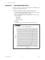
1
Introduction to NI ELVIS TM by Professor Barry Paton Dalhousie University Course Software Version 2.0 October 2005 Edition Part Number 323777C-01 Introduction to NI ELVIS Copyright © 2004–2005 National Instruments Corporation. All rights reserved. Universities, colleges, and other educational institutions may reproduce all or part of this publication for educational use. For all other uses, this publication may not be reproduced or transmitted in any form, electronic or mechanical, including photocopying, recording, storing in an information retrieval system, or translating, in whole or in part, without the prior written consent of National Instruments Corporation. Trademarks National Instruments, NI, ni.com, and LabVIEW are trademarks of National Instruments Corporation. Refer to the Terms of Use section on ni.com/legal for more information about National Instruments trademarks. Other product and company names mentioned herein are trademarks or trade names of their respective companies. Members of the National Instruments Alliance Partner Program are business entities independent from National Instruments and have no agency, partnership, or joint-venture relationship with National Instruments. Patents For patents covering National Instruments products, refer to the appropriate location: Help»Patents in your software, the patents.txt file on your CD, or ni.com/legal/patents. Worldwide Technical Support and Product Information ni.com National Instruments Corporate Headquarters 11500 North Mopac Expressway Austin, Texas 78759-3504 USA Tel: 512 683 0100 Worldwide Offices Australia 1800 300 800, Austria 43 0 662 45 79 90 0, Belgium 32 0 2 757 00 20, Brazil 55 11 3262 3599, Canada 800 433 3488, China 86 21 6555 7838, Czech Republic 420 224 235 774, Denmark 45 45 76 26 00, Finland 385 0 9 725 725 11, France 33 0 1 48 14 24 24, Germany 49 0 89 741 31 30, India 91 80 51190000, Israel 972 0 3 6393737, Italy 39 02 413091, Japan 81 3 5472 2970, Korea 82 02 3451 3400, Lebanon 961 0 1 33 28 28, Malaysia 1800 887710, Mexico 01 800 010 0793, Netherlands 31 0 348 433 466, New Zealand 0800 553 322, Norway 47 0 66 90 76 60, Poland 48 22 3390150, Portugal 351 210 311 210, Russia 7 095 783 68 51, Singapore 1800 226 5886, Slovenia 386 3 425 4200, South Africa 27 0 11 805 8197, Spain 34 91 640 0085, Sweden 46 0 8 587 895 00, Switzerland 41 56 200 51 51, Taiwan 886 02 2377 2222, Thailand 662 278 6777, United Kingdom 44 0 1635 523545 For further support information, refer to the Additional Information and Resources appendix. To comment on National Instruments documentation, refer to the National Instruments Web site at ni.com/info and enter the info code feedback. Contents Guide to Preparation for This Course Lab 1 NI ELVIS Workspace Environment Goal.............................................................................................................................1-2 Soft Front Panels Used in This Lab ............................................................................1-2 Components Used in This Lab....................................................................................1-2 Exercise 1-1 Measuring Component Values .........................................................1-3 Exercise 1-2 Building a Voltage Divider Circuit on the NI ELVIS Protoboard ...1-5 Exercise 1-3 Using the DMM to Measure Current................................................1-7 Exercise 1-4 Observing the Voltage Development of an RC Transient Circuit....1-8 Exercise 1-5 Visualizing the RC Transient Circuit Voltage..................................1-10 For Further Exploration ..............................................................................................1-13 Lab 2 Digital Thermometer Goal.............................................................................................................................2-1 Soft Front Panels Used in This Lab ............................................................................2-2 Components Used in This Lab....................................................................................2-2 Exercise 2-1 Measuring the Resistor Component Values .....................................2-3 Exercise 2-2 Operating the Variable Power Supply..............................................2-4 Exercise 2-3 Building a Thermistor Circuit for DAQ Operation ..........................2-6 Exercise 2-4 Building an NI ELVIS Virtual Digital Thermometer.......................2-8 For Further Exploration ..............................................................................................2-11 Lab 3 AC Circuit Tools Goal.............................................................................................................................3-2 Soft Front Panels Used in This Lab ............................................................................3-2 Components Used in This Lab....................................................................................3-2 Exercise 3-1 Measuring the Circuit Component Values .......................................3-3 Exercise 3-2 Measuring Component and Circuit Impedance Z ............................3-4 Exercise 3-3 Testing an RC Circuit with the Function Generator and Oscilloscope...............................................................................3-7 Exercise 3-4 The Gain/Phase Bode Plot of the RC Circuit ...................................3-11 For Further Exploration ..............................................................................................3-13 © National Instruments Corporation iii Introduction to NI ELVIS Contents Lab 4 Op Amp Filters Goal.............................................................................................................................4-1 Soft Front Panels Used in This Lab ............................................................................4-1 Components Used in This Lab....................................................................................4-1 Exercise 4-1 Measuring the Circuit Component Values .......................................4-2 Exercise 4-2 Frequency Response of the Basic Op Amp Circuit..........................4-3 Exercise 4-3 Measuring the Op Amp Frequency Characteristic ...........................4-6 Exercise 4-4 Highpass Filter..................................................................................4-8 Exercise 4-5 Lowpass Filter ..................................................................................4-11 Exercise 4-6 Bandpass Filter .................................................................................4-13 For Further Exploration ..............................................................................................4-15 Lab 5 Digital I/O Goal.............................................................................................................................5-2 Soft Front Panels Used in This Lab ............................................................................5-2 Components Used in This Lab....................................................................................5-2 Exercise 5-1 Visualizing Digital Byte Patterns .....................................................5-3 Exercise 5-2 555 Digital Clock Circuit .................................................................5-5 Exercise 5-3 Building a 4-Bit Digital Counter ......................................................5-8 Exercise 5-4 LabVIEW Logic State Analyzer ......................................................5-9 For Further Exploration ..............................................................................................5-11 Lab 6 Magnetic Field Sensor Goal.............................................................................................................................6-2 Soft Front Panels Used in This Lab ............................................................................6-2 Components Used in This Lab....................................................................................6-2 Exercise 6-1 Testing the Analog Magnetic Field Sensor with NI ELVIS Tools ...............................................................................6-3 Exercise 6-2 Hysteresis Characteristic of a Magnetic Field Switch......................6-5 Exercise 6-3 Counting Pulses with a Magnetic Switch Sensor .............................6-6 Exercise 6-4 Automatic Counting using a LabVIEW Program ............................6-7 For Further Exploration ..............................................................................................6-9 Lab 7 LEDs to the Rescue Goal.............................................................................................................................7-1 Soft Front Panels Used in This Lab ............................................................................7-2 Components Used in This Lab....................................................................................7-2 Exercise 7-1 Testing Diodes and Determining Their Polarity ..............................7-3 Exercise 7-2 Characteristic Curve of a Diode .......................................................7-5 Introduction to NI ELVIS iv ni.com Contents Exercise 7-3 Manual Testing and Control of a Two-Way Stoplight Intersection .......................................................................................7-8 Exercise 7-4 Automatic Operation of the Two-Way Stoplight Intersection .........7-12 For Further Exploration ..............................................................................................7-14 Lab 8 Free Space Optical Communication Goal.............................................................................................................................8-1 Soft Front Panels Used in This Lab ............................................................................8-2 Components Used in This Lab....................................................................................8-2 Exercise 8-1 A Phototransistor Detector ...............................................................8-3 Exercise 8-2 Infrared Red Optical Source.............................................................8-6 Exercise 8-3 Free Space IR Optical Link (Analog)...............................................8-8 Exercise 8-4 Amplitude and Frequency Modulation (Analog) .............................8-9 For Further Exploration ..............................................................................................8-10 Lab 9 RF Wireless Communication Goal.............................................................................................................................9-2 Soft Front Panels Used in This Lab ............................................................................9-2 Components Used in This Lab....................................................................................9-2 Exercise 9-1 The Transmitter ................................................................................9-3 Exercise 9-2 The Receiver.....................................................................................9-4 Exercise 9-3 Testing the RF Transmitter and Receiver.........................................9-5 Exercise 9-4 Building a Unique Test Signal with the Arbitrary Waveform Analyzer .........................................................................9-7 Exercise 9-5 A Demonstration of Marconi’s RF Transmission Signal .................9-10 For Further Exploration ..............................................................................................9-11 Lab 10 Mechanical Motion Goal.............................................................................................................................10-1 Soft Front Panels Used in This Lab ............................................................................10-2 Components Used in This Lab....................................................................................10-2 Exercise 10-1 Start Your Engine .............................................................................10-3 Exercise 10-2 The Tachometer................................................................................10-4 Exercise 10-3 Building a Rotary Motion System....................................................10-6 Exercise 10-4 Testing the Rotary Motion System...................................................10-7 Exercise 10-5 A LabVIEW Measurement of RPM .................................................10-8 For Further Exploration ..............................................................................................10-10 Appendix A Additional Information and Resources © National Instruments Corporation v Introduction to NI ELVIS Guide to Preparation for This Course The example programs in this course were created using the device name Dev1. Ensure that the DAQ device to which the NI ELVIS workstation connects is configured in NI-DAQmx as Dev1 as follows: 1. Open Measurement & Automation Explorer (MAX). 2. Under My System, expand Devices and Interfaces. 3. Expand NI-DAQmx Devices. 4. Find the DAQ device to which the NI ELVIS workstation connects and rename it Dev1 by right-clicking the device and selecting Rename from the list if it currently has a different name. 5. Close MAX. © National Instruments Corporation vii Introduction to NI ELVIS NI ELVIS Workspace Environment 1 The NI ELVIS environment consists of the following components: • Hardware workspace for building circuits and interfacing experiments • NI ELVIS software (created in LabVIEW), which includes the following: – Soft front panel (SFP) instruments – LabVIEW ELVIS API The NI ELVIS software includes additional LabVIEW VIs for custom control and access to the features of the NI ELVIS benchtop workstation. © National Instruments Corporation 1-1 Introduction to NI ELVIS Lab 1 NI ELVIS Workspace Environment Goal These exercises introduce the NI ELVIS workstation and demonstrate how you can measure electronic component properties. You can build circuits on the protoboard and later analyze them with the NI ELVIS software suite of LabVIEW-based SFPs, or software instruments. These exercises also demonstrate the use of NI ELVIS within the LabVIEW programming environment. Soft Front Panels Used in This Lab This lab requires the following SFPs: • Digital Ohmmeter, DMM[Ω] • Digital Capacitance, Meter DMM[C] • Digital Voltmeter, DMM[V] Components Used in This Lab This lab requires the following components: Introduction to NI ELVIS • 1.0 kΩ resistor, R1, (brown, black, red) • 2.2 kΩ resistor, R2, (red, red, red) • 1.0 MΩ resistor, R3, (brown, black, green) • 1 µF capacitor, C • FET Op Amp, such as an LM356 1-2 ni.com Lab 1 Exercise 1-1 NI ELVIS Workspace Environment Measuring Component Values Complete the following steps to measure component values: 1. Connect two banana-type leads to the DMM current inputs on the workstation front panel. 2. Connect the other ends to one of the resistors. 3. Launch NI ELVIS by double-clicking the NI ELVIS desktop icon. After initializing as shown in the figure below, the suite of LabVIEW software instruments opens. If you receive an error, check to see that the DAQ device cable is securely connected and that the NI ELVIS workstation is powered on. NI ELVIS may also be communicating with the incorrect DAQ device if you have multiple DAQ devices in the system. If more than one DAQ device is in the system, select the DAQ device used by NI ELVIS in the window that opens. Note © National Instruments Corporation 1-3 Introduction to NI ELVIS Lab 1 NI ELVIS Workspace Environment 4. Select Digital Multimeter. You can use the Digital Multimeter SFP for a variety of operations. The notation DMM[X] is used to signify the X operation. 5. A message box will open. Read the message and click OK. 6. Click the Null button. 7. Click the Ω (ohm) button to use the Digital Ohmmeter function DMM[Ω] to measure R1, R2, and R3. Fill in the following data: R1_______Ω (1.0 kΩ nominal) R2_______Ω (2.2 kΩ nominal) R3_______Ω (1.0 MΩ nominal) If the Function Generator is in manual mode, the resistance and capacitance buttons are grayed out. On the workstation, switch the manual mode of the function generator to off, in order to use the buttons. Note 8. Click the (capacitor) button and measure the capacitor C with DMM[C] using the same leads. Fill in the following data: C*_______(µf) (1 µF nominal) If you are using an electrolytic capacitor, be sure to connect the + lead of the capacitor to the DMM current + input and click the electrolytic button of the DMM[C]. Note End of Exercise 1-1 Introduction to NI ELVIS 1-4 ni.com Lab 1 Exercise 1-2 NI ELVIS Workspace Environment Building a Voltage Divider Circuit on the NI ELVIS Protoboard Complete the following steps to build a voltage divider: 1. Using the two resistors, R1 and R2, assemble the following circuit on the NI ELVIS protoboard. To +5V V0 + R1 V1 To DMM (Voltage HI) R2 – To Ground To DMM (Voltage LO) Common 2. Connect the input voltage, Vo, to the [+5V] pin socket. 3. Connect the common to the NI ELVIS [Ground] pin socket. 4. Connect the external leads to the DMM voltage inputs (HI) and (LO) on the front panel of the NI ELVIS workstation. NI ELVIS has separate input leads for voltage and impedance/current measurements. Note 5. Check the circuit, and then apply power to the protoboard by switching the Prototyping Board Power switch to the up position. The three power indicator LEDs, +15V, –15V, and +5V, should now be lit. © National Instruments Corporation 1-5 Introduction to NI ELVIS Lab 1 NI ELVIS Workspace Environment Notes If any of these LEDS are not lit while the others are lit and your protection board is the fused type, the fuse for that power line is probably blown. Refer to the NI ELVIS User Manual for fuse replacement information. If the protection board uses a resettable circuit for the power, a dim LED indicates a potential short in the circuit. If your protection board has resettable fuses, power cycle the NI ELVIS to reset the resettable fuses. 6. Move the front panel leads back to the DMM(VOLTAGE) inputs and select DMM[V]. 7. Connect the DMM front panel leads to, Vo, and measure the input voltage using the DMM[V]. According to circuit theory, the output voltage V1 is as follows: R2 V 1 = ----------------------- × V o ( R1 + R2 ) 8. Using the previously measured values for R1, R2, and Vo, calculate V1. Next, use the DMM[V] to measure the actual voltage, V1. V1 (calculated) _______________V1 (measured) ______________ 9. How well does the measured value agrees with the calculated value? End of Exercise 1-2 Introduction to NI ELVIS 1-6 ni.com Lab 1 Exercise 1-3 NI ELVIS Workspace Environment Using the DMM to Measure Current According to Ohms law, the current (I) flowing in the previous circuit is equal to V1/R2. 1. Using the measured values of V1 and R2, calculate the current. 2. Perform a direct measurement by moving the external leads to the workstation front panel DMM (Current) inputs HI and LO. 3. Connect the other ends to the circuit, as shown in the following figure. I To +5V V0 R1 V1 R2 To Ground To DMM (Current LO) To DMM (Current HI) 4. Select the function DMM[A] and measure the current. I (calculated) _______________ I (measured) ________________ 5. How well does the measured value agrees with the calculated value? End of Exercise 1-3 © National Instruments Corporation 1-7 Introduction to NI ELVIS Lab 1 NI ELVIS Workspace Environment Exercise 1-4 Observing the Voltage Development of an RC Transient Circuit Complete the following steps to observe the voltage development of an RC transient circuit: 1. Build the RC transient circuit as shown in the following figure. It uses the voltage divider circuit where R1 is now replaced with R3 (1 MΩ resistor), and R2 is replaced with the 1 µF capacitor C. 2. Move the front panel leads back to the DMM(VOLTAGE) inputs and select DMM[V]. To +5V To DMM (Voltage HI) To Ground To DMM (Voltage LO) The NI ELVIS version 1 workstation has limited input impedance (1 MΩ) for the DMM channel. To read the correct voltage values, you must buffer the input voltage for this measurement. Refer to the Limited Input Impedance Solution section for a simple solution using a unity gain circuit with a FET Op Amp. This limitation will be remedied in a future version. Using the analog input channels of the DAQ device as described in Exercise 1-5, prevents this problem. Note When the circuit is powered on, the voltage across the capacitor rises exponentially. Power on the circuit and watch the voltage change on the DMM display. It takes about five seconds to reach the steady state value of Vo. When you power off the circuit, the voltage across the capacitor falls exponentially to 0 V. Introduction to NI ELVIS 1-8 ni.com Lab 1 NI ELVIS Workspace Environment 3. Power up and then power off the circuit to observe the rise and fall of voltage. In Exercise 1-5 you will view this transient effect on a plot of capacitor voltage versus time. Limited Input Impedance Solution Using an FET Op Amp such as the LM356, build a unity gain circuit and connect it as shown in the following figure. By connecting the output (pin 6) to the – input (pin 2), the gain of this circuit is set to 1. However, the + input impedance (pin 3) is now hundreds of megaohms, and the output voltage (pin 6) follows the capacitor voltage allowing the DMM voltage input to read the correct values. +15 V To +5V 2 3 – 7 + 4 6 To DMM (Voltage HI) –15 V To Ground To DMM (Voltage LO) End of Exercise 1-4 © National Instruments Corporation 1-9 Introduction to NI ELVIS Lab 1 NI ELVIS Workspace Environment Exercise 1-5 Visualizing the RC Transient Circuit Voltage Complete the following steps to visualize the RC transient circuit voltage: 1. Remove the +5V power lead and replace it with a wire connected to the Variable Power Supply socket pin VPS[+], as shown in the following figure. 2. Connect the output voltage, V1, to ACH0[+] and ACH0[–]. VPS+ 1 MΩ ACH0+ C1 Ground 1 µF ACH0– 3. Close the NI ELVIS software suite and launch LabVIEW. 4. From the Hands-On NI ELVIS VI Library folder, select RC Transient.vi. This program uses the LabVIEW API to turn the power supply on for five seconds then off for five seconds while the voltage across the capacitor is displayed on a LabVIEW chart. This type of square wave excitation dramatically shows the charging and discharging characteristics of a simple RC circuit, as shown in the following illustration. The circuit time constant, τ, is defined as the product of R3 and C. Introduction to NI ELVIS 1-10 ni.com Lab 1 NI ELVIS Workspace Environment Kirchoff’s laws, show that the charging voltage VC across the capacitor is given by: VC – -t τ = V0 1 – e and the discharge voltage VD is given by: VD – -t- τ = V0 e You can extract the time constant from the measured chart. Observe the LabVIEW diagram window to see how this program works. © National Instruments Corporation 1-11 Introduction to NI ELVIS Lab 1 NI ELVIS Workspace Environment The following sequence of events occurs: 1. The VPS Initialize VI on the left starts NI ELVIS and selects the + power supply. 2. The Update VI sets the output voltage on VPS+ to 5 V. 3. The first sequence measures 50 sequential voltage readings across the capacitor. 4. In the For Loop, the DAQ Assistant VI takes 100 readings at rate of 1,000 samples per second and passes the values to an array. 5. The array is passed to the Mean VI, which returns the average value of the 100 readings. 6. The average is passed to the chart using a local variable terminal (RC Charging and Discharging). 7. The next sequence sets the VPS+ voltage equal to 0 V. 8. The last sequence measures another 50 averaged samples for the discharge cycle. End of Exercise 1-5 Introduction to NI ELVIS 1-12 ni.com Lab 1 NI ELVIS Workspace Environment For Further Exploration This chapter introduced the software instrument DMM and showed how you can use the workstation front panel connectors, shown in the following figure, for the DMM measurements. However, you are not restricted to using only these four DMM inputs. You can also use the four DMM inputs present on the protoboard strip sockets. © National Instruments Corporation 1-13 Introduction to NI ELVIS 2 Digital Thermometer A thermistor is a 2-wire device manufactured from semiconductor material. It has a nonlinear response curve and a negative temperature coefficient. Thermistors make excellent sensors for measuring temperature over a wide dynamic range. They are also useful in temperature alarm circuits. Goal This lab introduces the NI ELVIS variable power supply. You can use it with the workstation front panel controls, with the virtual controls on the computer screen, or embedded inside a LabVIEW program. The VPS is used to excite a 10 kΩ thermistor in a voltage divider circuit. The voltage measured across the thermistor is related to its resistance, which in turn is related to its temperature. This lab demonstrates how LabVIEW controls and indicators are used with NI ELVIS APIs to build a digital thermometer. © National Instruments Corporation 2-1 Introduction to NI ELVIS Lab 2 Digital Thermometer Soft Front Panels Used in This Lab This lab requires the following SFPs: • Digital Ohmmeter, DMM[Ω] • Digital Voltmeter, DMM[V] • VPS APIs Components Used in This Lab This lab requires the following components: Introduction to NI ELVIS • 10 kΩ resistor, R1, (brown, black, orange) • 10 kΩ thermistor, RT 2-2 ni.com Lab 2 Exercise 2-1 Digital Thermometer Measuring the Resistor Component Values Complete the following steps to observe the change in resistance across a thermistor: 1. Launch NI ELVIS. 2. Select Digital Multimeter and click the Ω button. 3. Connect the test leads to DMM (CURRENT). 4. Insert the 10 kΩ resistor and the thermistor into the prototype board. 5. Connect the DMM + and – probes to the 10 kΩ resistor and the thermistor individually, and measure the component values. 6. Fill in the following chart: 10 kΩ resistor_________________ Ω Thermistor___________________ Ω 7. Place the thermistor between your fingertips to heat it, and watch the resistance values change. The fact that the resistance decreases with increasing temperature (negative temperature coefficient) is one of the key characteristics of a thermistor. Thermistors are manufactured from semiconductor material whose resistivity depends exponentially on ambient temperature and results in the following nonlinear response. Compare the thermistor response with an RTD (100 Ω platinum resistance temperature device) shown in the following figure. 10 M Thermistor (2252 Ω at 25 ˚C) Resistance (Ω) 1M 100 k 10 k RTD (PT 100 Ω ) 1k 100 400 350 300 250 200 150 100 50 0 –50 –100 –150 –200 10 Temperature (˚C) Figure 2-1. Resistance-Temperature Curve of a Thermistor End of Exercise 2-1 © National Instruments Corporation 2-3 Introduction to NI ELVIS Lab 2 Digital Thermometer Exercise 2-2 Operating the Variable Power Supply Complete the following steps to take a measurement using the variable power supply: 1. From the NI ELVIS Instrument Launcher, select Variable Power Supplies. There are two controllable power supplies with NI ELVIS: 0 to –12 V and 0 to +12 V, each with a 500 mA current limit. 2. On the NI ELVIS workstation, slide the VPS+ switch to Manual. In manual mode, the controls on the VPS SFP are grayed out and you cannot use the controls. A green LED indicates that the VPS is in manual control. In manual mode only the front panel controls can change the output voltage. Note 3. Connect the leads from [VPS+] and [Ground] sockets of the NI ELVIS prototyping board to the workstation DMM voltage inputs. 4. Select DMM[V]. 5. Rotate the manual VPS knob on the workstation and observe the voltage change on the DMM[V]. The zero voltage position for VPS+ control is counter-clockwise (CCW) and for VPS– control is clockwise (CW). Note Introduction to NI ELVIS 2-4 ni.com Lab 2 Digital Thermometer 6. Slide the workstation switch for VPS+ down (not Manual). Now you can use the virtual VPS controls on the computer screen. 7. Click and drag the virtual knob to change the output voltage. Notes The RESET button quickly resets the voltage back to 0. VPS– works in a manner similar to VPS+, except the output voltage is negative when using VPS–. End of Exercise 2-2 © National Instruments Corporation 2-5 Introduction to NI ELVIS Lab 2 Digital Thermometer Exercise 2-3 Building a Thermistor Circuit for DAQ Operation Complete the following steps to build and test a thermistor circuit: 1. On the workstation protoboard, build a voltage divider circuit using the 10 kΩ resistor and a thermistor. The input voltage is wired to [VPS+] and [Ground] sockets. 2. Measure the voltage across the thermistor with the DMM[V] and workstation leads. To VPS+ R1 To DMM (Voltage HI) RT Thermistor To DMM (Voltage LO) To Ground Figure 2-2. Thermistor Circuit 3. Make sure the workstation VPS+ knob is set CCW (0 V position) and the slide switch is set to Manual. 4. Power on the protoboard and observe the voltage levels on the DMM[V]. As you increase the voltage from 0 to +5 V, the voltage across the thermistor, VT, should increase to about 2.5 V. 5. Reduce the power supply voltage to +3 V. 6. Heat the thermistor with your fingertips and watch the voltage decrease. You can now rearrange the standard voltage divider equation to calculate the thermistor resistance as follows: R1 × VT R T = --------------------------3 volts – V T At an ambient temperature of 25 °C, the resistance should be about 10 kΩ. This equation, called a scaling function, allows you to convert the measured voltage into the thermistor resistance. You can easily measure VT with the NI ELVIS DMM or within a LabVIEW program (VI). Introduction to NI ELVIS 2-6 ni.com Lab 2 Digital Thermometer In LabVIEW, the previous scaling equation is coded as a subVI and looks like the following block diagram: A typical thermistor response curve demonstrates the relationship between device resistance and temperature. It is clear from this curve that a thermistor has the following three characteristics: • The temperature coefficient ∆R/∆T is negative. • The response curve is nonlinear (exponential). • The resistance varies over several decades; refer to Figure 2-1. You can produce a calibration curve by fitting a mathematical equation to the response curve. LabVIEW has many mathematical tools to fit such a relationship. When the correct equation is found, you can calculate the temperature for any resistance within the calibrated region. The following calibration VI is typical for a thermistor and demonstrates how you can use the LabVIEW formula node to evaluate mathematical equations. End of Exercise 2-3 © National Instruments Corporation 2-7 Introduction to NI ELVIS Lab 2 Digital Thermometer Exercise 2-4 Building an NI ELVIS Virtual Digital Thermometer The digital thermometer program activates the VPS to power on the thermistor circuit. It then reads the voltage across the thermistor and converts it into temperature. The basic program is a variation of the Simple Variable Power Supply Application found in the NI ELVIS User Manual. The following figure shows the digital thermometer diagram. NI ELVIS has the same Device Number (usually Dev1) as the DAQ device. The NI ELVIS VPS Initialization VI selects VPS Supply+, and then the voltage level on the power supply is set with the NI ELVIS - Update VI, which sets the VPS output to +3 V. Measurement, scaling, calibration, and display occur in sequence within the While Loop. VoltsIn.vi measures the thermistor voltage. Scaling.vi converts the measured voltage to resistance according the scaling equation above. Convert R-T.vi uses a known calibration equation to convert the thermistor resistance into temperature. Finally, the temperature is displayed on the LabVIEW front panel in a variety of formats. The Wait function of 100 milliseconds ensures the voltage is sampled every 0.1 seconds. The digital thermometer continues running until the Stop button on the front panel button is activated or an error occurs. When the loop ends, the supply reference is closed and the VPS is set to 0 V. Introduction to NI ELVIS 2-8 ni.com Lab 2 Digital Thermometer Complete the following steps to open and view the components and code in the digital thermometer VI: 1. From the Hands-On NI ELVIS VI Library folder, open Digital Thermometer.vi. 2. Open the program and subVIs to view the program flow and see how the subVIs and the Read and Convert functions are coded. With the calibration equation for the thermistor, you can update the subVI (Convert R-T) with the proper equation and use it to have a functioning digital thermometer. If you want to write your own program, you can use DT Template.vi (found in the Hands-On NI ELVIS VI Library folder) and add your programming style. The VPS API functions are located in Functions» All Functions»Instrument I/O»Instrument Drivers»NI ELVIS» Variable Power Supplies. © National Instruments Corporation 2-9 Introduction to NI ELVIS Lab 2 Digital Thermometer The simple digital thermometer program displays the following three indicators on the front panel: • Digital display • Meter • Thermometer Often, only one or two display formats are required when performing measurements with NI ELVIS. However, adding a logging feature makes it possible to observe the temperature trend. In DT Logger.vi (found in the Hands-On NI ELVIS VI Library folder), a chart on the front panel is added. You can add this feature as a single LabVIEW control (Waveform Chart) on the front panel, found by selecting the Controls/Graph menu. From the Hands-On NI ELVIS VI Library folder, load and view DT Logger.vi. End of Exercise 2-4 Introduction to NI ELVIS 2-10 ni.com Lab 2 Digital Thermometer For Further Exploration You can use NI ELVIS VPS with workstation front panel controls, SFPs, or within a LabVIEW program to build a custom instrument. There are many other features you can add to the digital thermometer program, such as a [Hold/Update] button with which you can sample and hold the current value on a digital display. By toggling a button, you can update the temperature. Open the Sample_HoldThermometer VI from the Hands on ELVIS Library folder to see how this feature is implemented in LabVIEW. You can also plot ∆T versus time to determine the reference temperature. © National Instruments Corporation 2-11 Introduction to NI ELVIS 3 AC Circuit Tools Many electronic circuits contain alternating current (AC). Designing good circuits requires tools used to measure components and impedance, and the tools to display circuit properties. With good tools and minimal circuit knowledge, you can modify any circuit to give optimal response. © National Instruments Corporation 3-1 Introduction to NI ELVIS Lab 3 AC Circuit Tools Goal This lab introduces the NI ELVIS tools for AC circuits: a digital multimeter, function generator, oscilloscope, impedance analyzer, and Bode analyzer. Soft Front Panels Used in This Lab This lab requires the following SFPs: • Digital Ohmmeter, DMM[Ω/C] • Function Generator, FGEN • Oscilloscope, OSC • Impedance Analyzer • Bode Analyzer Components Used in This Lab This lab requires the following components: Introduction to NI ELVIS • 1 kΩ resistor, R, (brown, black, red) • 1 µF capacitor, C 3-2 ni.com Lab 3 Exercise 3-1 AC Circuit Tools Measuring the Circuit Component Values Complete the following steps to obtain the values of the circuit components: 1. Launch NI ELVIS. 2. Select Digital Multimeter. 3. Connect the test leads to DMM (CURRENT). 4. Use the DMM[Ω] to measure the resistor, R. 5. Use DMM[C] to measure the capacitor, C. 6. Fill in the following values: Resistor R Capacitor C _________________ Ω (1 kΩ nominal) _________________ µF (1 µF nominal) 7. Close the DMM window. End of Exercise 3-1 © National Instruments Corporation 3-3 Introduction to NI ELVIS Lab 3 AC Circuit Tools Exercise 3-2 Measuring Component and Circuit Impedance Z For a resistor, the impedance is the same as the DC resistance. You can represent it on a 2-D plot as a line along the x-axis, which is often called the real component. For a capacitor, the impedance (or more specifically, the reactance), XC, is imaginary, depends on frequency, and is represented as a line along the y-axis of a 2-D plot. It is called the imaginary component. Mathematically, the reactance of a capacitor is represented by the following equation: 1X C = --------jωC where ω is the angular frequency (measured in radians/sec) and j is a symbol used to represent an imaginary number. The impedance of an RC circuit in series is the sum of these two components where R is the resistive (real) component and XC is the reactive (imaginary) component. 1 Z = R + X C = R + ---------- Ω jωC You can also represent this as a phasor vector on a polar plot with Magnitude = 2 R + XC 2 and –1 X C Phase θ = tan ------ R A resistor has a phasor along the real (X) axis. A capacitor has a phasor along the negative imaginary (Y) axis. Recall from complex algebra that 1--- = – j j Introduction to NI ELVIS 3-4 ni.com Lab 3 AC Circuit Tools Complete the following steps to visualize this phasor in real time: 1. Select Impedance Analyzer from the NI ELVIS Instrument Launcher menu. 2. Connect leads from the front panel DMM (current) inputs to the 1 kΩ resistor. 3. Verify that the phasor is along the real axis and the phase is zero. 4. Connect the leads to the capacitor. 5. Verify that the phasor is along the negative imaginary axis and that the phase is 270 or –90 degrees. 6. Adjust the Measurement Frequency control box to observe that the reactance (length of the phasor) gets smaller when you increase the frequency, and larger when you decrease the frequency. 7. Connect the leads across the resistor and capacitor in series (verify the circuit is not connected to ground). The circuit phasor has both a real and an imaginary component. 8. Change the frequency and watch the phasor move. © National Instruments Corporation 3-5 Introduction to NI ELVIS Lab 3 AC Circuit Tools 9. Adjust the frequency until the absolute value of the reactance component (X) is equal to the absolute value of the resistance component (R). This is a special frequency value where the phase is 45°. The magnitude also has special meaning at this frequency or phase angle. What is the magnitude of the phasor at this point? Answer: R 2 10. Close the Impedance Analyzer window. End of Exercise 3-2 Introduction to NI ELVIS 3-6 ni.com Lab 3 Exercise 3-3 AC Circuit Tools Testing an RC Circuit with the Function Generator and Oscilloscope Complete the following steps to build and test an RC circuit: 1. On the workstation protoboard, build a voltage divider circuit using a 1 µF capacitor and a 1 kΩ resistor. 2. Connect the RC circuit inputs to [FUNCOUT] and [Ground] pin sockets, as shown in the following figures. To FUNCOUT 1 F ACH0+ 1k ACH0– To Ground © National Instruments Corporation 3-7 Introduction to NI ELVIS Lab 3 AC Circuit Tools The power supply for an AC circuit is often a function generator, which you can use to test the RC circuit. 3. From the NI ELVIS Instrument Launcher, select Function Generator. The FGEN SFP has the following controls, which you can use to do the following: • set the Frequency by decades (Course) and by Hz (Fine) • select the waveform type (Sine, Square, or Triangle) • select the waveform amplitude All of these controls are also available on the workstation front panel. You can select them by sliding the workstation front panel function generator switch to Manual. As with the Variable Power Supply, manual control turns on the green LED display on the SFP and grays out the virtual controls. If you want to add a DC offset to the AC signal, it is only available on the FGEN SFP. Note Introduction to NI ELVIS 3-8 ni.com Lab 3 AC Circuit Tools You can use the oscilloscope to analyze the voltage signals of the RC circuit by completing the following steps: 1. From the NI ELVIS Instrument Launcher, select Oscilloscope. The oscilloscope SFP is similar to most oscilloscopes, but the NI ELVIS oscilloscope can automatically connect inputs to a variety of sources. 2. Click the CHANNEL A Source drop-down list. 3. Set the Source on CHANNEL A, Source on CHANNEL B, TRIGGER, and TIMEBASE inputs as shown in the previous figure. This configuration allows the oscilloscope to measure the output of the function generator on channel A, the FGEN TTL synchronization signal (SYNC_OUT) on channel B, and be triggered with the SYNC_OUT signal. 4. Click the Run button of the FGEN SFP and the OSC SFP. 5. Play with the FGEN controls (virtual or real) and observe the changes on the oscilloscope window. © National Instruments Corporation 3-9 Introduction to NI ELVIS Lab 3 AC Circuit Tools There are measurement options, such as frequency and Amplitude P-P, that are accessed by clicking the MEAS buttons for either channel A or B. Measurements show up at the bottom of the oscilloscope screen. You can activate the cursors for channel A or B to make amplitude and time measurements. 6. Connect the workstation BNC SCOPE input CH B to the 1 kΩ resistor. You can also use the channel B inputs on the protoboard pin sockets labeled Oscilloscope CH B+ and CH B–. Note The following conditions are true: • The input signal is still on channel A. • The output signal for the RC circuit is on channel B. • The trigger is still on the FGEN SYNC_OUT. • Select a Sine wave on the FGEN. The ratio of the amplitude on channel B to the amplitude on channel A defines the circuit gain at a particular frequency. Because there is no amplifier in the circuit, the gain is less than one. By looking at different frequencies, you can get a feel for the frequency characteristics of the RC passive filter circuit. Challenge Find the frequency for which the gain equals 2 . On the oscilloscope screen, measure the phase difference between the channel A trace and channel B trace at this frequency. Can you relate this phase measurement to the Phasor phase measurement found with the Impedance Amplifier in Exercise 3-2? Close the function generator and oscilloscope. End of Exercise 3-3 Introduction to NI ELVIS 3-10 ni.com Lab 3 Exercise 3-4 AC Circuit Tools The Gain/Phase Bode Plot of the RC Circuit A Bode plot defines in a real graphical format the frequency characteristics of an AC circuit. Amplitude response is plotted as the circuit gain measured in decibels as a function of log frequency. Phase response is plotted as the phase difference between the input and output signals on a linear scale as a function of log frequency. Complete the following steps to build an RC circuit and measure the gain and phase Bode plots of the circuit: 1. From the NI ELVIS Instrument Launcher, select Bode Analyzer. The Bode Analyzer allows you to scan over a range of frequencies, from a start frequency to a stop frequency in steps of ∆F. You can also set the amplitude of the test sine wave. The Bode Analyzer uses the SFP function generator to generate the test waveform. You must connect the FUNCOUT output sockets to the test circuit and to ACH1. The output of the circuit under test goes to ACH0+. You can find further information by clicking the HELP button on the lower right corner of the Bode Analyzer window. 2. Rebuild the RC circuit on the NI ELVIS protoboard, similar to the following circuit, and make connections as shown in Exercise 3-3. © National Instruments Corporation 3-11 Introduction to NI ELVIS Lab 3 AC Circuit Tools FUNCOUT ACH1+ 1 F ACH0+ 1k ACH0– To Ground ACH1– 3. Verify that the circuit is connected as shown in the previous figure and click the Run button. 4. Use the Display options to select the graphing format, and use the cursors to read points off the frequency characteristic. The frequency where the signal amplitude has fallen to –3 dB is the same frequency where the phase is 45 degrees. Note End of Exercise 3-4 Introduction to NI ELVIS 3-12 ni.com Lab 3 AC Circuit Tools For Further Exploration Both the Oscilloscope and Bode Analyzer SFPs have a Log button. When activated, the data presented on the graphs is written to a spreadsheet file on the hard drive. For further analysis you can read this data with Excel, LabVIEW, DIAdem, or another analysis or plotting program. The following figure shows a sample log file. 11/07/2003 4:09 PM Amplitude: 2.00 V Frequency (Hz), Gain (dB), Phase (dig) 5.000, –11.313, 73.929 6.295, –9.341, 69.780 7.924, –7.661, 65.278 9.976, –6.104, 60.025 12.559, –4.649, 54.057 15.811, –3.507, 48.012 19.905, –2.504, 41.384 25.059, –1.735, 34.955 31.548, –1.177, 29.064 39.716, –0.779, 23.805 50.000, –0.512, 19.374 62.946, –0.292, 14.617 79.245, –0.195, 11.932 99.763, –0.122, 9.445 © National Instruments Corporation 3-13 Introduction to NI ELVIS 4 Op Amp Filters Adding a few capacitors and resistors to the basic Op Amp circuit yields many interesting analog circuits, such as active filters, integrators, and differentiators. Filters are used to pass specific frequency bands, integrators are used in proportional control, and differentiators are used in noise suppression and waveform generation circuits. Goal This lab uses the NI ELVIS suite of instruments to measure the characteristics of a lowpass, highpass, and bandpass filter. Soft Front Panels Used in This Lab This lab requires the following SFPs: • Digital Multimeter, DMM [Ω, C] • Function Generator, FGEN • Oscilloscope, OSC • Impedance Analyzer • Bode Analyzer Components Used in This Lab This lab requires the following components: • 10 kΩ resistor, R1, (brown, black, orange) • 100 kΩ resistor, Rf, (brown, black, yellow) • 1 µF capacitor, C1 • 0.01 µF capacitor, Cf • 741 Op Amp © National Instruments Corporation 4-1 Introduction to NI ELVIS Lab 4 Op Amp Filters Exercise 4-1 Measuring the Circuit Component Values Complete the following steps to measure the values of the individual circuit components: 1. Launch NI ELVIS. 2. Select Digital Multimeter. 3. Use DMM[Ω] to measure the resistors. 4. Use DMM[C] to measure the capacitors. 5. Fill in the following information. R1 ___________ Ω (10 kΩ nominal) Rf ___________ Ω (100 kΩ nominal) C1 ___________ µF (1 µF nominal) Cf ___________ µF (0.01 µF nominal) 6. Close the DMM. End of Exercise 4-1 Introduction to NI ELVIS 4-2 ni.com Lab 4 Exercise 4-2 Op Amp Filters Frequency Response of the Basic Op Amp Circuit Complete the following steps to build and perform measurements on an Op Amp circuit: 1. On the workstation protoboard, build a simple 741 inverting Op Amp circuit with a gain of 10, as shown in the following schematic diagram. Rf R1 V 1 (To FUNCOUT) +15 V 2 3 – 741 + 7 6 (To CHA+) 4 –15 V (To CHA–) The following figure shows what the circuit looks like on the NI ELVIS protoboard. The Op Amp uses both the +15 V and –15 V DC power supplies. These are found on the protoboard pin sockets (labeled as +15V, –15V, and Ground). 2. Connect the Op Amp input voltage V1 to [FUNCOUT]. 3. Connect the [Ground] pin sockets. © National Instruments Corporation 4-3 Introduction to NI ELVIS Lab 4 Op Amp Filters 4. Connect the Op Amp output voltage Vout to the oscilloscope input pin sockets [CHA+] and [CHA–]. 5. From the NI ELVIS Instrument Launcher, select Function Generator and Oscilloscope. 6. On the Oscilloscope SFP, set CHANNEL A Source to BNC/Board CH A. To view the input signal, set CHANNEL B Source to FGEN FUNC_OUT. This shortcut on channel B allows you to link the channel B input to the oscilloscope without any additional wiring. Note 7. On the function generator panel, set the following parameters: • Waveform: Sine wave • Peak Amplitude: 0.1 V • Frequency: 1000 Hz • DC Offset: 0.0 V 8. Check the circuit, and then power on the protoboard. 9. Run the FGEN and OSC continuous mode. The test voltage V1 is shown on channel B and the Op Amp output voltage Vout on channel A. 10. Because the test signal originates from FGEN, select SYNC_OUT for the trigger source. Introduction to NI ELVIS 4-4 ni.com Lab 4 Op Amp Filters 11. Measure the amplitude of the Op Amp input (CH B) and output (CH A) from the Oscilloscope window. The output signal is inverted with respect to the input. This is expected for an inverting Op Amp circuit. 12. Calculate the voltage gain (the amplitude ratio channel A/channel B). Try a range of frequencies from 100 Hz to 10 kHz. Observe any changes. How do the measurements agree with the theoretical gain of (Rf /R1)? You can also use an analog trigger source from CH A or CH B. This choice sets the Trigger Type to Analog (SW), allowing you to set the trigger slope and level. Note 13. Close the FGEN and OSC windows. End of Exercise 4-2 © National Instruments Corporation 4-5 Introduction to NI ELVIS Lab 4 Op Amp Filters Exercise 4-3 Measuring the Op Amp Frequency Characteristic The best way to study the AC characteristic response curve of the Op Amp is to measure its Bode plot. The Bode plot is basically a plot of Gain (dB) and Phase (degrees) as a function of log frequency. The transfer function for an Inverting Op Amp circuit is given by: Rf V out = - ------ V 1 R1 where Vout is the Op Amp output and V1 is the Op Amp input (the amplitude of FGEN in the circuit). The Gain is the quantity (Rf /R1). The minus sign inverts the output signal with respect to the input signal. On a Bode plot, you expect a straight line with a magnitude of 20 × log (Gain). For a gain of 10, the Bode amplitude should be 20 dB. Complete the following steps to measure the Bode plot of the Op Amp circuit: 1. From the NI ELVIS Instrument Launcher, select Bode Analyzer. 2. Connect the signals, input (V1), and output (Vout), to the analog input pins as follows: • V1 → ACH1+ (from the FUNCOUT) Ground → ACH1– • Vout → ACH0+ (from the Op Amp Output) Ground → ACH0– 3. From the Bode Analyzer, set the scan parameters as follows: • Start: 5 (Hz) • Stop: 50000 (Hz) • Steps: 10 (per decade) 4. Click Run and observe the Bode plot for the Inverting Op Amp circuit. 5. Observe the phase response. Introduction to NI ELVIS 4-6 ni.com Lab 4 Op Amp Filters The gain is flat until approximately 10,000 Hz, where it starts to roll off, as shown in the following graph. This graph is as expected because the high frequency response of an Op Amp depends on the circuit gain in the high frequency limit. For this lab, take this curve as the basic Bode plot for a 741 Op Amp. End of Exercise 4-3 © National Instruments Corporation 4-7 Introduction to NI ELVIS Lab 4 Op Amp Filters Exercise 4-4 Highpass Filter Complete the following steps to modify the Op Amp circuit and perform a frequency measurement: 1. Add a 1 µF capacitor Cl in series with the 1 kΩ input resistor R1 in the Op Amp circuit as shown in the following figure. The low frequency cutoff point fL is given by the equation: 1 2πf L = -----------R1 C1 where fL is measured in Hertz. The low frequency cutoff point is the frequency where the Gain (dB) has fallen by –3 dB. This point (–3 dB) occurs when the impedance of the capacitor equals that of the resistor. The highpass Op Amp filter equation is similar. At the –3 dB point, the impedance of the input resistor is equal to the impedance of the input capacitor: 1 - = X R 1 = ---------------------C ( 2πf L C 1 ) Rf R1 V 1 (To FUNCOUT) +15 V C1 – A (To CHA+) + –15 V (To CHA–) Introduction to NI ELVIS 4-8 ni.com Lab 4 Op Amp Filters The following figure shows the circuit on the NI ELVIS protoboard. 2. Run a second Bode plot using the same scan parameters as in Exercise 4-3. 3. Observe that the low frequency response is attenuated, while the high frequency response is similar to the basic Op Amp Bode plot. © National Instruments Corporation 4-9 Introduction to NI ELVIS Lab 4 Op Amp Filters 4. Use the cursor function to find the low frequency cutoff point, which is the frequency at which the amplitude has fallen by –3 dB or the phase change is 45 degrees. 5. Compare your results with the following theoretical prediction: 1 2πf L = -----------R1 C1 End of Exercise 4-4 Introduction to NI ELVIS 4-10 ni.com Lab 4 Exercise 4-5 Op Amp Filters Lowpass Filter The high-frequency rolloff in the Op Amp circuit is due to the internal capacitance of the 741 chip being in parallel with the feedback resistor Rf . If you add an external capacitor, Cf , in parallel with the feedback resistor Rf , you can reduce the upper frequency cutoff point to fU. You can predict the new cutoff point from the equation: 1 2πf U = ---------Rf Cf Complete the following steps to perform an additional frequency measurement on the Op Amp circuit: 1. Short circuit the input capacitor (do not remove it, as you will use this in Exercise 4-6). 2. Add the feedback capacitor Cf in parallel with the 100 kΩ feedback resistor, as shown in the following figure. Cf Rf +15 V R1 V 1 (To FUNCOUT) – A (To CHA+) + –15 V (To CHA–) © National Instruments Corporation 4-11 Introduction to NI ELVIS Lab 4 Op Amp Filters 3. Run a third Bode plot using the same scan parameters. The following graph shows the high frequency response is attenuated more than the basic Op Amp response. 4. Use the cursor function to find the high frequency cutoff point, that is, the frequency at which the amplitude has fallen by –3 dB or the phase change is 45 degrees. 5. Compare your results with the following theoretical prediction: 1 2πf U = ---------Rf Cf End of Exercise 4-5 Introduction to NI ELVIS 4-12 ni.com Lab 4 Exercise 4-6 Op Amp Filters Bandpass Filter If you allow both an input capacitor and a feedback capacitor in the Op Amp circuit, the response curve has both a low cutoff frequency, fL, and a high cutoff frequency, fU. The frequency range (fU – fL) is called the bandwidth. For example, a good stereo amplifier would have a bandwidth of at least 20,000 Hz. The following figure shows a bandpass filter on the NI ELVIS protoboard. Remove the short on C1 and run a fourth Bode plot using the same scan parameters. The following graph shows the results of using the bandpass filter. © National Instruments Corporation 4-13 Introduction to NI ELVIS Lab 4 Op Amp Filters By drawing a line at 3 dB below the maximum amplitude region, the frequency range contained by all frequencies above this line defines the bandpass. End of Exercise 4-6 Introduction to NI ELVIS 4-14 ni.com Lab 4 Op Amp Filters For Further Exploration The generalized Op Amp transfer curve is given by the phasor equation: Zf V out = ----- V in Z 1 where the Impedance values for the four circuits are: Op Amp Zf Z1 Gain Basic Rf R1 Rf / R1 Highpass Rf R1 + XC1 Rf / (R1 + XC1) Lowpass Rf + XCf R1 (Rf + XCf) / R1 Bandpass Rf + XCf R1 + XC1 (Rf + XCf) / (R1 + XC1) For any frequency, you can use the Impedance Analyzer to measure the impedances Zf and Z1. A LabVIEW program can calculate the ratio of two complex numbers. The magnitude of the ratio |Zf /Z1| is the gain. Note You can also use the Impedance Analyzer to find the frequencies where R1 equals XC1 and Rf equals XCf to verify that the lower and upper frequency cutoff points from the Bode plot are equal to these frequencies. © National Instruments Corporation 4-15 Introduction to NI ELVIS 5 Digital I/O Digital electronics is the heart and soul of modern computers. The ability to set and read digital lines is essential to digital circuit diagnostics. Figure 5-1. Typical NI ELVIS Protoboard Circuit © National Instruments Corporation 5-1 Introduction to NI ELVIS Lab 5 Digital I/O Goal This lab focuses on the NI ELVIS digital tools, such as a digital clock, digital counter, and a logic state analyzer to study circuits. Soft Front Panels Used in This Lab This lab requires the following SFPs: • Digital Writer • Digital Reader • Oscilloscope Components Used in This Lab This lab requires the following components: Introduction to NI ELVIS • 10 kΩ resistor, RA, (brown, black, orange) • 100 kΩ resistor, RB, (brown, black, yellow) • 1 µF capacitor, C • 555 Timer chip • 7493 4-bit binary counter 5-2 ni.com Lab 5 Exercise 5-1 Digital I/O Visualizing Digital Byte Patterns The NI ELVIS protoboard has a bank of eight green LEDs with pin sockets LED <0..7>. You can use them as visual indicators of digital logic states (On = HI and Off = LO). Complete the following steps to output digital patterns using the Digital Writer: 1. Wire the LEDs to the 8-bit parallel output bus sockets pins DO <0..7>. For example, connect DO 0 to the pin socket LED 0. Only one lead is required because the grounds are connected internally within NI ELVIS. The digital output pins are located in the upper right-hand corner of the NI ELVIS protoboard. Note 2. Launch the NI ELVIS Instrument Launcher. 3. Select Digital Writer. A new digital logic diagnostic window opens, which allows you to set/reset any of the write lines to a HI or LO state. The Digital Output (DO) bits are labeled 0 to 7, reading right to left in the Manual Pattern box, as shown in the following figure. You can set/reset (HI/LO) on any bit by clicking the top or bottom portion of the virtual switch. Collectively, these eight bits constitute a byte, which you can read in a binary, hexadecimal, or decimal format in the display box above the switches. © National Instruments Corporation 5-3 Introduction to NI ELVIS Lab 5 Digital I/O 4. After a digital pattern is set, click Write (green arrow) to send the pattern to the parallel output port DO <0..7>, which in turn are passed onto the green LEDs. You can set the Mode to output a single pattern or to continuously output the pattern. In continuous operation, the hardware is updated continuously with the current pattern displayed in software. Note The set pattern is echoed on blue LED indicators of the Bus State on the SFP. Also, in the Action box SFP, you can Toggle, Rotate, or Shift the bit pattern right or left. 5. Click the Stop (red box) button to cease updating the port. In testing digital circuits, there are several patterns often used for diagnostic checks. 6. Click the Pattern selector on the SFP to view the options available. • Manual Load any 8-bit pattern • Ramp (0–255) Computer Instruction INC • Alternating 1/0s Computer Instruction INVERT • Walking 1s Computer Instruction SHIFT LEFT LOGIC 7. Try to output each bit pattern. 8. Close the Digital Bus Writer window. End of Exercise 5-1 Introduction to NI ELVIS 5-4 ni.com Lab 5 Exercise 5-2 Digital I/O 555 Digital Clock Circuit You can configure a 555 timer chip, together with resistors RA, RB, and capacitor C, to act as a digital clock source. Complete the following steps to build and perform measurements on a 555 digital clock circuit: 1. Using the DMM[Ω] and DMM[C], measure the component values and fill in the following: RA ______________________ Ω(10 kΩ nominal) RB ______________________ Ω (100 kΩ nominal) C ______________________ µF (1 µF nominal) 2. Build the clock circuit on the protoboard as shown in the following figure. Vcc → +5 V 4 RA 8 555 7 6 RB 2 C Discharge 3 Output To NI ELVIS DI 0 Line Threshold Trigger 1 Power (+5 V) goes to pins 8 and 4, and the ground goes to pin 1. The timing chain of RA, RB, and C straddles the power supply. It has a connection between the resistors going to pin 7 and a connection between RB and C going to pins 2 and 6. 3. Wire the 555 output pin 3 to the parallel input port pin socket DI 0. The digital input pins <DIO 0..7> are located in the upper right-hand corner of the NI ELVIS protoboard. Note © National Instruments Corporation 5-5 Introduction to NI ELVIS Lab 5 Digital I/O 4. From the NI ELVIS Instrument Launcher, select Digital Reader, check your circuit, and enable power to the protoboard on the NI ELVIS workstation. The Digital Bus Reader allows the current state of the parallel input port to be read on demand (single shot) or continuously. If the clock circuit is running correctly and continuously—as shown in the previous figure—you should see the least significant bit flashing. If not, use the DMM[V] to check the voltage on the 555 pins. With the clock circuit running, you can now make some useful circuit measurements. The 555 Timer oscillator circuit has a Period T of: T = 0.695 ( R A + 2R B )C seconds The 555 Timer oscillator circuit frequency is related to the period by: 1 F = --- Hz T The 555 Timer oscillator circuit has a Duty Cycle (On time/Period) of: ( RA + RB ) DC = --------------------------( R A + 2R B ) 5. Close all SFPs and click the Oscilloscope button. 6. Connect the front panel BNC Scope CH A input leads to pin 3 of the 555 Timer chip and any ground. You should now observe the digital waveform on channel A of the oscilloscope. 7. Select Trigger Source CH A. This option takes the signal from channel A, sets the Trigger Type to [Analog (SW)] and allows you to set the Trigger slope and Level. Set the Level to +1 V. 8. Utilizing the [MEAS] option for channel A, observe the frequency in the scope window. 9. Turn CURSORS CH A button [ON] by clicking and dragging the cursors 10. Measure the period and duty cycle. Introduction to NI ELVIS 5-6 ni.com Lab 5 Digital I/O 11. Fill in the following information: T ___________________ (seconds) Ton __________________ (seconds) DC _________________ (volts) F ___________________ (Hz) 12. Compare the measurements with the previous theoretical predictions. 13. Close any SFPs. End of Exercise 5-2 © National Instruments Corporation 5-7 Introduction to NI ELVIS Lab 5 Digital I/O Exercise 5-3 Building a 4-Bit Digital Counter Complete the following steps to build a 4-bit digital counter: 1. Insert a 7493 4-bit binary ripple counter into the protoboard next to the 555 digital clock circuit. This chip contains a divide-by-two and a divide-by-eight counter. 2. Configure the chip as a divide-by-sixteen counter by jumpering pin 12 (Q1) to pin 1 Clock 2 on the 7493 chip, as shown in the following figure. Vcc → +5 V Q2 Q4 Q8 Q1 +5 V 8 4 RA 7 RB C2 555 6 2 12 5 Discharge 3 Threshold Output → Clock Input 14 C1 ÷2 1 C = 1 µF 9 8 11 ÷8 10 Trigger C 1 2 3 0set GND 7493 4-Bit Binary Counter 3. On the 7493 binary counter chip, connect +5 V power to pin 5, and ground to pin 10. 4. Ensure that the 0set, and pins 2 and 3 are grounded. 5. Connect the outputs Q1, Q2, Q4, and Q8 to the LED and digital input ports of the NI ELVIS protoboard using the following mapping scheme: • Q1 pin 12 to LED 4 and DI 4 • Q2 pin 9 to LED 5 and DI 5 • Q4 pin 8 to LED 6 and DI 6 • Q8 pin 11 to LED 7 and DI 7 • 555 Clock pin 3 to LED 0 and DI 0 6. Connect the 555 digital clock output (pin 3) to the 7493 clock1 input (pin 14). 7. Power on the chips and watch the binary counts accumulate on the LEDs. 8. From the NI ELVIS Instrument Launcher, select Digital Reader. This allows you to monitor the binary states on the computer and at the same time view the states on the green LEDs. 9. Close NI ELVIS. End of Exercise 5-3 Introduction to NI ELVIS 5-8 ni.com Lab 5 Exercise 5-4 Digital I/O LabVIEW Logic State Analyzer The exercises up to this point, have only covered the state of digital outputs at one point in time. This exercise shows how a timing diagram is formed by stringing sequential states together sampled uniformly in time. Plotting several digital lines together on the same graphs generates a digital timing diagram as illustrated below. A binary counter has a unique timing diagram where the following falling edge of the previous bit causes the next bit to toggle. Using the LabVIEW APIs for digital I/O, you can build a simple 4-bit logic state analyzer. The Digital I/O palette is located in Functions»All Functions»Instrument I/O»Instrument Drivers»NI ELVIS. The top row of DIO VIs (from left to right) are Initialize, Read, Write, and Close. Launch LabVIEW and select Binary Counter.vi from the Hands-On NI ELVIS Library folder. © National Instruments Corporation 5-9 Introduction to NI ELVIS Lab 5 Digital I/O On the diagram panel, the NI ELVIS DIO icon (on the left) initializes the Read function on Dev1 (default) and creates a refnum (green line). The middle DIO icon reads the port and the DIO icon (on the right) closes the DIO operation freeing up any memory used in running the program and passing any error messages onto the front panel. The 4-bit logic state analyzer samples the NI ELVIS parallel port (NI ELVIS DIO – Read.vi) and presents the bits as a numeric number (blue line). LabVIEW converts the numeric number into an 8-bit Boolean array (thick green line). Bit 4 on the port (Q1) is mapped to the fifth element (index 4) of the array. The Index Array VI extracts a particular bit, for example (index 4), and sends Q1 to the Trace 0 and then onto the plot routine. Each Boolean bit is converted back to a numeric value (either 0 or 1) and then bundled together with the other traces for plotting the timing diagram for Q1, Q2, Q3, and Q4. The many formats of LabVIEW chart options allow the data presentation in an expected format for a timing diagram. End of Exercise 5-4 Introduction to NI ELVIS 5-10 ni.com Lab 5 Digital I/O For Further Exploration If you are using a 74393 IC (8-bit binary counter), you can modify the previous LabVIEW program to build an 8-bit logic state analyzer. © National Instruments Corporation 5-11 Introduction to NI ELVIS 6 Magnetic Field Sensor In 1879, Edwin Hall discovered that when a current flows through a block of semiconductor material in the presence of a magnetic field, a voltage is generated across it. He found that this voltage, now named after him, was equal to the vector cross product of the current and magnetic field. VH = γ I × B + ε – X X X X X X B in X X ω I X X X X – –q Vd X X X X X X ––––––––––––– F X X X X X X I X X X X X X X X X X X X +++++++++++++ I This means that you can use a Hall probe to measure current, magnetic field, or the angle between the sensor axis and an external field. Today, integrated Hall Effect sensors have an internal constant current source and an Op Amp amplifier to buffer the output signal. These sensors are inexpensive, robust, and can be interfaced to both analog and digital circuits. © National Instruments Corporation 6-1 Introduction to NI ELVIS Lab 6 Magnetic Field Sensor Goal This lab focuses on using NI ELVIS tools to study the properties of Hall Effect sensors. During the lab, a simple Gaussmeter and a digital counter interface are built using a linear Hall Effect sensor and a Hall Effect switch, respectively. Soft Front Panels Used in This Lab This lab requires the following SFPs: • DMM[V] • Oscilloscope, OSC • LabVIEW VIs for the Digital Counter Components Used in This Lab This lab requires the following components: • Small horseshoe magnet • Linear Magnetic Field Sensor Allegro A3240UA • Hall Effect Switch Allegro A3212UA. Contact Allegro at www.allegro.com to request a free sample of these sensors. Introduction to NI ELVIS 6-2 ni.com Lab 6 Exercise 6-1 Magnetic Field Sensor Testing the Analog Magnetic Field Sensor with NI ELVIS Tools The Allegro devices have three terminals: +Vcc power, Gnd, and the Hall output. Complete the following steps to install and perform measurements on a Hall Effect sensor: 1. Insert a linear Hall device (A3240) into the protoboard. 2. Connect the power +5V pin socket to the +Vcc. 3. Connect the ground pin socket to Ground. 4. Connect the DMM (voltage) leads to the Hall output and Ground. Top View Hall IC 1 2 3 To +5 V Hall Voltage to DMM (Voltage HI) Ground Lead to DMM (Voltage LO) Hall Voltage To Ground 5. Launch the NI ELVIS Instrument Launcher and select Digital Multimeter. 6. Bring a small magnet (field intensity of several hundred gauss) in close proximity to the face of the Hall sensor. In the absence of a magnetic field, the sensor reads one half of +Vcc or about +2.5 V. As you bring the magnet closer to the sensor, the Hall voltage either rises greater than 2.5 V or falls to less than 2.5 V depending on the magnet polarity. The south end of the magnet causes a rise, the north end a fall. The sensor saturates near +5 or 0 V in a field in excess of ±500 gauss. The Hall voltage is quite nonlinear with the distance between the sensor and the magnet face. 7. To observe this relationship, make distance and voltage measurements and then plot the observations. The distance between adjacent pin socket holes is 0.1 in. 8. Place the magnet on the protoboard directly in front of the sensor and measure the Hall voltage in 0.1 or 0.05 in. increments over a distance of about 1 in. © National Instruments Corporation 6-3 Introduction to NI ELVIS Lab 6 Magnetic Field Sensor 9. Record each reading in the following table. Distance (in.) Reading Distance (in.) 0.05 0.55 0.10 0.60 0.15 0.65 0.20 0.70 0.25 0.75 0.30 0.80 0.35 0.85 0.40 0.90 0.45 0.95 0.50 1.00 Reading 10. Plot the Hall voltage versus distance. The plot should be similar to the following graph. The response is quite nonlinear. This demonstrates the importance of knowing the operating distance between the sensor and the magnet. End of Exercise 6-1 Introduction to NI ELVIS 6-4 ni.com Lab 6 Exercise 6-2 Magnetic Field Sensor Hysteresis Characteristic of a Magnetic Field Switch Complete the following steps to perform measurements on the Hall Effect switch to determine its hysteresis characteristics: 1. Replace the linear sensor with the Hall Effect switch A3212. The power connections are the same as the linear circuit. 2. Repeat the measurements for Hall voltage versus distance for both an increasing and a decreasing distance. 3. Plot each graph on the same set of axes. It should look similar to the following graph. The Hall switch is a digital sensor whose output is either HI (~ +5 V) or LO (0.8 V). A critical field Bmax exists above which the output is always HI and a critical field Bmin below which the output is LO. A graph of Hall Voltage versus range from sensor demonstrates hysteresis between the response of approaching the sensor and of leaving the sensor. The difference between the two limits: h = B max – B min is a measure of the noise immunity of the sensor. For example, if the sensor takes a particular field to switch from LO to HI, it then requires a much smaller field (Bmax – h) to switch to the opposite state HI to LO. Because you are using a fixed magnet, you can translate these critical fields from previous exercise into critical positions. 4. Close the Digital Multimeter. End of Exercise 6-2 © National Instruments Corporation 6-5 Introduction to NI ELVIS Lab 6 Magnetic Field Sensor Exercise 6-3 Counting Pulses with a Magnetic Switch Sensor Complete the following steps to perform a pulse count measurement using the Hall Effect Switch: 1. Place the magnet far enough away from the sensor so it is in the LO state. 2. Move the south end of a magnet toward the sensor. The magnetic field eventually exceeds Bmax and the logic state toggles HI. Then, as the magnet is pulled away and the magnetic field becomes less than Bmin, it switches back to the LO state. The entire sequence LO-HI-LO generates a positive pulse. Repeating this operation numerous times generates a train of positive pulses. 3. From the NI ELVIS Instrument Launcher, select Oscilloscope. 4. Connect the workstation front panel BNC connector (CH A) to the output signal from the Hall Effect switch (pins 3 and 2). 5. On the oscilloscope panel: • Select Channel Source BNC/Board CH A and the following: – Source: CH A – Type: Analog – Slope: Rising – Level: 2 V 6. Observe the Hall voltage on channel A as you rapidly move the magnet toward and away from the sensor. With the oscilloscope trace on a long time base (100 ms/div), you can observe the pulse train. An angle shaft encoder, a tachometer, and a dwell sensor all use magnetic switches to generate pulses. Counting pulses accumulates events. Counting pulses within a select time interval measures frequency. Next, you will use a LabVIEW VI to count pulses generated by the sensor. 7. Close all SFPs and remove the voltage probe. End of Exercise 6-3 Introduction to NI ELVIS 6-6 ni.com Lab 6 Exercise 6-4 Magnetic Field Sensor Automatic Counting using a LabVIEW Program Complete the following steps to perform an automatic counting operation using a LabVIEW VI: 1. Connect the output of the Hall Effect switch to the following NI ELVIS counter inputs: • Hall Output (pin 3) to CTR0_SOURCE • Hall Ground (pin1) to GROUND 2. Launch LabVIEW. 3. From the Hands-On NI ELVIS Library folder, select Hall Counter.vi. This simple program allows you to accumulate counts as a magnetic field is passed in and out from the Hall effect switch. Dividing the accumulated counts by the Elapsed (count) time generates the average time per count or the frequency. © National Instruments Corporation 6-7 Introduction to NI ELVIS Lab 6 Magnetic Field Sensor NI ELVIS has access to the DAQ device counters, and this lab uses Dev1, Counter 0. The program uses the DAQ Assistant to control the DAQ device counters. Two [Tick Count] functions are used to measure the timing interval. End of Exercise 6-4 Introduction to NI ELVIS 6-8 ni.com Lab 6 Magnetic Field Sensor For Further Exploration In Exercise 6-1, you manually collected data and then plotted a graph. However, using the NI ELVIS APIs for the digital voltmeter DMM[V] within LabVIEW, you can build a simple program to collect the Hall data on-demand, in a semi-automated solution. Complete the following steps to use a LabVIEW to automate data collection from the Hall device: 1. From the Hands-On NI ELVIS Library folder, select Hall Sample.vi. 2. Place the magnet a known distance in front of the linear Hall sensor (A3240) and enter the end face position of the magnet in the Position box. 3. Click the Sample button when ready. This data point (Position, Hall Voltage) is automatically entered into an array of sampled points. 4. When you have finished sampling, click Plot to open the graph. 5. Open the diagram panel, shown in the following figure, to view the program flow. © National Instruments Corporation 6-9 Introduction to NI ELVIS 7 LEDs to the Rescue A property of an electronic diode is that in one direction current flows easily (forward biased), while in the other direction current flow is blocked. The simple switching nature of diodes, an OFF state and an ON state, yields many interesting analog and digital circuits. Goal This lab focuses on using NI ELVIS to illuminate diode properties, diode test methods, bit patterns for a two-way stop light intersection, and the use of NI ELVIS APIs in a LabVIEW program to run the stoplights automatically. © National Instruments Corporation 7-1 Introduction to NI ELVIS Lab 7 LEDs to the Rescue Soft Front Panels Used in This Lab This lab requires the following SFPs: • Digital Diode tester, DMM[ ] • Two-wire Current-Voltage Analyzer • Digital Writer Components Used in This Lab This lab requires the following components: Introduction to NI ELVIS • Silicon diode • Six light emitting diodes (2 red, 2 yellow, and 2 green) • Six 220 Ω resistors 7-2 ni.com Lab 7 Exercise 7-1 LEDs to the Rescue Testing Diodes and Determining Their Polarity A semiconductor junction diode is a polar device often labeled on one end with a band called the cathode; the other lead is called the anode. While there are many ways to indicate this polarity in the packaging of a diode, one thing is always the same—a positive voltage applied to the anode results in the diode being forward biased so that current can flow. You can use NI ELVIS to figure out the diode polarity. Complete the following steps to set up the NI ELVIS for diode and polarity tests: 1. Launch the NI ELVIS Instrument Launcher and select DMM. 2. Click the button. 3. Connect one of the LEDs to the workstation leads DMM (current) HI and LO. When the diode blocks the current, the display shows the same value as it does when no diode is connected (open circuit). When the diode allows current to flow, the LED gives off light and the display reads a voltage level less than the open circuit value. Run current through a red LED in both directions. When you see light, the diode lead connected to the LO or black banana jack is the cathode. You can use this simple test on other diodes to determine their polarity. For a silicon rectifying diode in the forward bias direction, the display shows a voltage less than 3.5 V and displays the word Good, as shown in the following figure. © National Instruments Corporation 7-3 Introduction to NI ELVIS Lab 7 LEDs to the Rescue In the reverse bias direction, the display shows the open circuit value (~3.5 V) and displays the word Open, as shown in the following figure. Run this test to see these results. The way this works is that the display shows the voltage required to generate a small current flow of about 1 mA. In the forward bias region, this voltage level is small and related to the materials used in the manufacture of the diode. In the reverse bias direction, no current flows and the tester displays the open circuit voltage, about 3.5 V. End of Exercise 7-1 Introduction to NI ELVIS 7-4 ni.com Lab 7 Exercise 7-2 LEDs to the Rescue Characteristic Curve of a Diode The characteristic curve of a diode, that is, a plot of the current flowing through the device as a function of the voltage across the diode, best displays its electronic properties. Complete the following steps to display the characteristic curve of a diode: 1. Place the silicon diode across the DMM (current) leads. Make sure the cathode is connected to the black banana input. 2. Launch the NI ELVIS Instrument Launcher and select Two Wire Current-Voltage Analyzer. A new SFP opens that allows you to display the (I -V) curve for the device under test. This SFP applies a test voltage to the diode from a starting voltage level to an ending level in incremental voltage steps all of which you can select. 3. For a silicon diode, set the following parameters: • Start –2 V • Stop +2.0 V • Increment 0.1 V 4. Set the maximum current in either direction to ensure the diode does not operate in a current region where damage can occur. 5. Click Run to see the I-V curve. © National Instruments Corporation 7-5 Introduction to NI ELVIS Lab 7 LEDs to the Rescue In the reverse bias direction, the current should be very small (µA) and negative. In the forward bias direction, you should see that above a threshold voltage, the current rises exponentially to the maximum current limit. 6. Change the Display buttons [Linear/Log] to see the curve plotted on a different scale. 7. Try the Cursor operation. It gives the (I,V) coordinate values as you drag the cursor along the trace. The threshold voltage is related to the semiconductor material of the diode. For silicon diodes, the threshold voltage is about 0.6 V, while for germanium diodes it is about 0.3 V. One way to estimate the threshold voltage is to fit a tangent line in the forward bias region near the maximum current (refer to the following figure). At the point where the tangent intersects, the voltage axis defines the threshold voltage. Observe the (I,V) characteristic curve for a light emitting diode. The threshold Voltage VT is given by the intersection of the tangent line with the voltage axis. Introduction to NI ELVIS 7-6 ni.com Lab 7 LEDs to the Rescue 8. Using the Two Wire Current-Voltage Analyzer, determine the threshold voltage for a red, yellow, and green LED, and fill in the following information: Red LED ____________ V Yellow LED ____________ V Green LED ____________ V Did you observe any trend? End of Exercise 7-2 © National Instruments Corporation 7-7 Introduction to NI ELVIS Lab 7 LEDs to the Rescue Exercise 7-3 Manual Testing and Control of a Two-Way Stoplight Intersection Complete the following steps to build, and manually test and control a two-way stoplight intersection simulation: 1. Install two each of red, yellow, and green LEDs on the NI ELVIS protoboard, positioned as a two-way stoplight intersection. To Ground Each LED is controlled by one binary bit on the 8-bit parallel bus on the NI ELVIS protoboard. Output pin sockets are labeled DO <0..7>. 2. Connect the pin socket DO 0 through a 220 Ω resistor to the anode of the red LED in the north-south (up-down) direction. 3. Connect the other end of the LED to one end of a 220 Ω resistor. Note Introduction to NI ELVIS The resistor is used to limit the current through the LED. 7-8 ni.com Lab 7 LEDs to the Rescue 4. Connect the other end of the 220 Ω resistor to the ground. The following figure illustrates this circuit. DO X LED 5. Connect the remaining colored LEDs in a similar fashion. Here is the complete mapping scheme. DO 0 Red N-S direction DO 4 Red E-W direction DO 1 Yellow N-S direction DO 5 Yellow E-W direction DO 2 Green N-S direction DO 6 Green E-W direction 6. From the NI ELVIS Instrument Launcher, select Digital Writer. 7. Using the vertical slide switches, select any 8-bit pattern and output it to the NI ELVIS digital lines. Recall that Bit 0 is connected to the pin socket on the protoboard labeled DO 0. 8. Set the Mode to Continuous and Pattern to Manual, as shown in the following figure. © National Instruments Corporation 7-9 Introduction to NI ELVIS Lab 7 LEDs to the Rescue 9. To activate the port, click the Write button. When all switches (bits 0–2 and 4–6) are HI, all the LEDs should be lit. When all these switches are LO, all the LEDs should be off. You can now use these switches to find out what 8-bit codes are necessary to control the various cycles of a stoplight intersection. Here are some clues for the intersection. The basic operation of a stoplight is based on a 60 second time interval with 30 seconds for red, followed by 25 seconds for green, followed by 5 seconds for yellow. For a two-way intersection the yellow light, say in the North-South direction is on while the red light in the East-West direction is also on. This modifies the 30 second red timing interval to two timing intervals, a 25 second cycle followed by a 5 second cycle. There are four timing periods (T1, T2, T3, and T4) for a two-way intersection. 10. Study the following chart to see how a two-way stoplight intersection works. LEDs North-South East-West Timing Period Timing Interval (seconds) R Y G R Y G 0 1 2† 4 5 6† 8-Bit Code Numeric Value T1 25 0 0 1 1 0 0 00010100 20 T2 5 0 1 0 1 0 0 T3 25 1 0 0 0 0 1 T4 5 1 0 0 0 1 0 † Bit number. R = red, Y = yellow, and G = green 11. Use the Digital Writer to determine what 8-bit code needs to be written to the digital port to control the stop lights in each of the four timing intervals. For example: T1 requires the code, 00101000. Computers read the bits in the reverse order (least significant bit on the right). The above code then becomes 00010100. In the previous table, you can read the radix of the switch pattern in binary 00010100, decimal 20,or hexadecimal 14. Introduction to NI ELVIS 7-10 ni.com Lab 7 LEDs to the Rescue 12. Click the white X in a gray background next to the Numeric Value to change the radix. You can use this feature to determine the numeric codes for the other timing intervals T2, T3, and T4. Now, if you output the 8-bit code for each of the timing intervals in sequence, you can manually operate the stoplights. Repeating this four-cycle sequence automates to the intersection. End of Exercise 7-3 © National Instruments Corporation 7-11 Introduction to NI ELVIS Lab 7 LEDs to the Rescue Exercise 7-4 Automatic Operation of the Two-Way Stoplight Intersection Complete the following steps to automate the timing cycle on the stoplight circuit: 1. Close NI ELVIS and launch LabVIEW. 2. Open the program, StopLights.vi. There is only one control on the SFP—a Boolean switch used to stop the operation of the stoplights. 3. Switch to the block diagram (Window»Show Block Diagram). 4. Observe the four-cycle sequence generated by the For Loop. The subVI icon with the pencil icon (NI ELVIS DIO-Write) is the structure that outputs the 8-bit code to the stoplights. This subVI expects the code input to be a numeric number. For example, the first timing interval, T1, requires the code 20 (twenty numeric). You must transfer the four 8-bit codes (numeric value) from the table in Exercise 7-3 into the four blank elements of the code array (blue) labeled Output Pattern. The NI ELVIS DIO - Initialize subVI on the left requires the digital port and the I/O operation (write). Like all NI ELVIS programming structures, the DIO channel must be closed by the subVI, NI ELVIS DIO - Close, on the right after completion (While Loop is stopped). Introduction to NI ELVIS 7-12 ni.com Lab 7 LEDs to the Rescue The timing intervals are stored in the four elements of the Time Delay array (orange). To speed up operation, the 25 second time interval is reduced to 5 seconds, and the 5 second time interval is reduced to 1 second. End of Exercise 7-4 © National Instruments Corporation 7-13 Introduction to NI ELVIS Lab 7 LEDs to the Rescue For Further Exploration LEDs are amazing devices. If you multiply the threshold voltage, VT by the electronic charge, e, the product is energy and it is close to the band gap energy of the semiconductor material used in the manufacture of the semiconductor diode. Further, in the forward biased region, the light from the LED has an energy of hc/λ where h is Planck’s constant, c is the speed of light, and λ is the wavelength of the center of the energy distribution. Conservation of energy yields the equation: eV ∼ hc ------ T λ where e is the electron charge. From the LED specifications, you can determine the wavelength or color of the LED. For example, red LEDs have a wavelength of about 560 nanometers. From the I-V characteristic curve of the LED, shown in Exercise 7-2, you can measure the threshold voltage VT. If you plot VT versus 1/λ for the three different colored LEDs, you will find a straight line with a slope approximately equal to hc/e, a fundamental constant. Introduction to NI ELVIS 7-14 ni.com Free Space Optical Communication 8 You are familiar with a number of remote controllers lying around the house such as those controlling televisions, stereos, and DVD players. Do you know how these controllers work? The secret is an infrared optical data link, a type of free space optical communications link. Figure 8-1 shows an example circuit on the protoboard. Figure 8-1. Free Space Infrared Optical Digital Communications Link Goal This lab uses an infrared optical source to communicate information over free space to a phototransistor detector. Several modulation schemes, including amplitude modulation and Non-Return-Zero (NRZ) digital modulation, are featured. © National Instruments Corporation 8-1 Introduction to NI ELVIS Lab 8 Free Space Optical Communication Soft Front Panels Used in This Lab This lab requires the following SFPs: • Two Wire I-V Analyzer • Three-wire I-V Curve Tracer • Function Generator • Oscilloscope • Digital Writer Components Used in This Lab This lab requires the following components: 1. • 220 Ω resistor (red, red, brown) • 470 Ω resistor (yellow, violet, brown) • 1 kΩ resistor (brown, black, red) • 22 kΩ resistor (red, red, orange) • 0.01 µF capacitor • IR Emitter (LED) • IR Detector (photoresistor)1 • 2N3904 NPN transistor • 555 Timer chip The RS276-142 IR Emitter and Detector pair are available at www.radioshack.com. Introduction to NI ELVIS 8-2 ni.com Lab 8 Exercise 8-1 Free Space Optical Communication A Phototransistor Detector Understanding how a phototransistor works starts with understanding transistor characteristic curves. A transistor is basically a current-controlled current amplifier. A small base current controls the current flowing through the transistor from the collector to the emitter. Complete the following steps to use a phototransistor to develop characteristic curves current curves at different base voltages: 1. Insert a 2N3904 transistor into the pin sockets labeled 3-WIRE, CURRENT HI, and CURRENT LO on the protoboard, as shown in the following figure. CURRENT HI is the base, CURRENT LO is the emitter, and 3-WIRE is the collector lead. Note 2. Launch the NI ELVIS Instrument Launcher and select Three-Wire Current-Voltage Analyzer. 3. Power on the protoboard. 4. Set the Base Current and Collector Voltage as shown in the following figure and click Run. © National Instruments Corporation 8-3 Introduction to NI ELVIS Lab 8 Free Space Optical Communication The graph shows the Collector Current versus Collector Voltage for different values of the base current. You can set many parameters for the Collector Voltage and the Base Current ranges. When run, this SFP first outputs the set base current, then outputs the collector voltage, and finally measures the collector current. Data points (I,V) are plotted and sequential points with the same base current are connected with a line. You can see the curves developed quickly, resulting in a family of [IV] curves with different individual base currents. Observe that for a given collector voltage, the collector current increases with an increase in base current. A phototransistor has no Base lead. Instead, light falling on the transistor generates a base current proportional to the light intensity. For example, with no light, the transistor follows the bottom (yellow) curve. A low light level follows the middle (red) curve and a higher light intensity generates the upper (green) curve. For collector voltages greater than 0.2 V, such as 1.0 V, the collector current follows the light intensity falling on the base region in an almost linear fashion. To build an optical detector, all that you need is a power supply, a current limiting resistor, and a phototransistor as shown in the following figure. Introduction to NI ELVIS 8-4 ni.com Lab 8 Free Space Optical Communication +5 V Phototransistor Output 470 Ω GND 5. Close any SFPs. End of Exercise 8-1 © National Instruments Corporation 8-5 Introduction to NI ELVIS Lab 8 Free Space Optical Communication Exercise 8-2 Infrared Red Optical Source The optical transmitter is made up of two components: an IR LED (forward biased) and a current-limiting resistor. Complete the following steps develop a simple optical data link: 1. Connect the IR LED to the DMM current inputs. Make sure the black lead is connected to the LED anode (short lead). 2. Select the Two-Wire Current-Voltage Analyzer and set the voltage sweep parameters to: • Start: 0.0 V • Stop: +2.0 V • Increment: 0.05 V 3. Click Run. The [IV] curve for the infrared diode is developed and displayed. Introduction to NI ELVIS 8-6 ni.com Lab 8 Free Space Optical Communication In the forward bias region, the IR LED emits light for voltages greater than about 0.9 V. Light is emitted at a wavelength of 950 nm, outside the spectral range of human eyesight and in the near infrared region. The LED specs tell us that the maximum allowed current is over 100 mA, making IR LEDs about 10 times brighter than normal visible LEDs. This is what gives the remote controllers so much range. Connecting the LED in series with a 220 Ω resistor and a +5 V power supply produces a current of about 17 mA yielding about 10 mW of invisible optical power. It takes a special detector like the phototransistor to see it. 4. Build the LED transmitter circuit and the phototransistor circuit on the protoboard, as shown in the following figure. Transmitter Detector To FUNC OUT +5 V Phototransistor IR LED 220 Ω GND 470 Ω To ACH0 GND 5. Connect the LED power source to the output of the function generator. 6. Connect the output of the phototransistor to ACH0 pin sockets. Taken together, these circuits form a simple optical data link. The following figure shows this circuit on the NI ELVIS protoboard: 7. Close any SFPs. End of Exercise 8-2 © National Instruments Corporation 8-7 Introduction to NI ELVIS Lab 8 Free Space Optical Communication Exercise 8-3 Free Space IR Optical Link (Analog) Complete the following steps to observe the transmitted and received signal of a free space IR optical link: 1. From the NI ELVIS Instrument Launcher, select Function Generator and Oscilloscope. The function generator provides the analog signal to be transmitted. The oscilloscope monitors the input signal CH A (Select FUNC_OUT) and the output signal CH B (Select ACH0). To transmit an analog signal on the LED, it is necessary to bias the LED into the linear region with a voltage greater than the critical voltage. 2. Make sure the function generator is not set for Manual mode on the front panel workstation. 3. On the FGEN SFP, set the offset voltage to +1.5 V. 4. Set the following parameters on the FGEN SFP: • Amplitude: 0.5 V • Voltage: +1.5 V • Waveform: Sine • Frequency: 1000 Hz 5. Run the function generator and oscilloscope, and observe the transmitted and received signals. 6. Change the offset voltage and amplitude levels. When the received sine wave starts to distort, the transmitter becomes nonlinear. 7. Find the best values of offset and amplitude for a linear (no distortion) transmission link. The link is now ready to send data. 8. Leave the function generator and oscilloscope SFPs open. End of Exercise 8-3 Introduction to NI ELVIS 8-8 ni.com Lab 8 Exercise 8-4 Free Space Optical Communication Amplitude and Frequency Modulation (Analog) Complete the following steps to build an elementary free space optical communication link: 1. Wire the digital-to-analog output pin sockets DAC0 and DAC1 to the function generator pin sockets on NI ELVIS protoboard labeled AM IN Amplitude Modulation and FM IN Frequency Modulation, respectively. 2. Launch LabVIEW. Select Modulation.vi from the Hands-On NI ELVIS Library folder. This program sends DC signals from NI ELVIS DAC output to the function generator to produce an amplitude or frequency modulated signal. The modulated signal is converted to light pulses, sent across the free space link and then detected on the phototransistor and converted back into an electrical signal. You have just built an elementary free space optical communication link for analog signals. 3. Close any SFPs and LabVIEW. End of Exercise 8-4 © National Instruments Corporation 8-9 Introduction to NI ELVIS Lab 8 Free Space Optical Communication For Further Exploration NRZ Digital Modulation IR remote controllers use a special encoding scheme called NRZ. A HI level is signaled by a tone burst of 40 KHz square waves while a LO level is signaled by the absence of any signal. The tone burst is generated using the 555 Timer circuit shown in the following figure. A digital switch is connected to pin 4 [RESET], so that when the switch is HI, a tone burst is generated. When the switch is LO, no oscillations occur. To Digital Write Line Vcc → +5 V 1.0 kΩ RA Transmitter 4 8 Detector 3 +5 V 7 10.0 kΩ RB 6 555 IR LED Phototransistor + 2 220 Ω C 470 Ω 1 To ACH0 – GND GND To demonstrate the modulation scheme, use a 1.0 kHz tone burst so it is easier to view with the oscilloscope. Complete the following steps build a gated oscillator: 1. Build a gated oscillator using a 555 timer chip and the following components: • RA: 1.0 kΩ • RB: 10.0 kΩ • C: 0.1 µF 2. Connect pin 4 on the 555 timer chip to the digital line DO 0 output parallel port on the NI ELVIS protoboard. 3. Connect the oscillator output pin 3 to the IR LED transmitter power source. 4. Connect the output of the detector circuit to ACH0 pin sockets. 5. Connect pin 1 of the 555 timer chip to the ground. Introduction to NI ELVIS 8-10 ni.com Lab 8 Free Space Optical Communication 6. From the NI ELVIS Instrument Launcher, select the Oscilloscope and Digital Writer. 7. For the oscilloscope, select CHANNEL A Source as ACH0. Use the Channel A analog trigger with a trigger level at 0.5 V. In operation, every time you set bit 0 (DO 0) of the Digital Writer to HI, a 1.0 kHz signal appears on the oscilloscope. No signal is presented when Bit 0 is LO. Try some of the other digital patterns like Walking 1’s or Ramp, and view the modulation scheme on the Oscilloscope SFP. In remote controllers, the encoding scheme is slightly more complicated. If you are interested in building a computer-controlled IR remote transmitter to control an item such as a stereo, refer to Sensors, Transducers and LabVIEW, by Barry E. Paton, for details. © National Instruments Corporation 8-11 Introduction to NI ELVIS RF Wireless Communication 9 Midday at Signal Hill, St. John’s Newfoundland, Canada, Guglielmo Marconi pressed his ear to a telephone head set connected to an experimental wireless receiver. 1,700 miles away at Poldu Cornwall, England, his co-workers were about to send the Morse code letter S, which is three dots. Faintly, but clearly psht-psht-psht pause psht-psht-psht came through the earphone. The date was December 12, 1901, and the first Trans-Atlantic message has just been sent and received. © National Instruments Corporation 9-1 Introduction to NI ELVIS Lab 9 RF Wireless Communication Goal In this lab, a paper clip antenna is used to send this classic message and other waveforms over a wireless radio frequency link. The NI ELVIS function generator is the transmitter and a high gain Op Amp is the receiver. The classic message is formulated using the NI ELVIS arbitrary waveform generator. Soft Front Panels Used in This Lab This lab requires the following SFPs: • Oscilloscope, OSC • Arbitrary Waveform Generator, ARB Components Used in This Lab This lab requires the following components: Introduction to NI ELVIS • 1 kΩ resistor (brown, black, red) • Two 100 kΩ resistors (brown, black, yellow) • 741 Op Amp or FET Op Amp 753 • 7408 digital IC • Paper clip 9-2 ni.com Lab 9 Exercise 9-1 RF Wireless Communication The Transmitter Complete the following steps to build a simple antenna from a paper clip: 1. Straighten a paper clip and cut it into a 2.5 in. long piece. 2. Push one end of the paper clip into the output pin socket of the function generator. When FGEN is running, the output voltage leaks out of the pin socket to the paper clip antenna and radiates a small RF signal. A similar antenna about a centimeter away can pick up this signal and amplify it to a higher signal level. You will use the transmitter in Exercise 9-2 1 2 1 Straight Paperclip 2 Stepped Paperclip Figure 9-1. Paperclip Antenna 3. Initially, use a sine wave to test the transmitter by setting the SFP function generator to sine waveform, 2.5 V amplitude, and 10000 Hz frequency. End of Exercise 9-1 © National Instruments Corporation 9-3 Introduction to NI ELVIS Lab 9 RF Wireless Communication Exercise 9-2 The Receiver Complete the following steps to build the receiver: 1. Bend a second paper clip into a step shape, with the long side about 2.5 in. long, the step height about 0.25 in., and the step width about 0.5 in. 2. Insert the short end of the paperclip into a pin socket. The mid-section supports the antenna on the protoboard and allows you to rotate the antenna about the short end. The long side sits vertical and is parallel to the transmitter antenna, as shown in Figure 9-1. 3. Build a high gain amplifier using a 741 Op Amp or 753 FET Op Amp in the simple noninverting configuration. +15 V Antenna 100 kΩ 3 100 kΩ 2 1 kΩ + 7 – 4 6 ACH 5 + 741 –15 V 4. Connect the 1 kΩ resistor to the – input (pin 2). 5. Connect a 100 kΩ bias resistor to the + input (pin 3). 6. Connect the other end of the resistors to AIGND. 7. Connect the other 100 kΩ resistor for the feedback resistor Rf from pin 2 to 6. 8. To power the circuit, connect +15 V on pin 7 and –15 V on pin 4. Nominally the Op Amp has a gain of 101. You can use other resistor combinations for higher gains. 9. Connect the receiver antenna to the input (pin 3). 10. Connect the Op Amp output pin 6 to the oscilloscope. End of Exercise 9-2 Introduction to NI ELVIS 9-4 ni.com Lab 9 Exercise 9-3 RF Wireless Communication Testing the RF Transmitter and Receiver A sine wave signal is used to test the transmitter-receiver pair. Complete the following steps: 1. Check the circuit you built in Exercise 9-2, then power on the protoboard. 2. Move the receiver antenna a few millimeters away from the transmitter antenna. 3. Connect the oscilloscope workstation BNC CH A inputs to the Op Amp output, pin 6, and ground. Typical oscilloscope settings are: • Channel A: ACH5 • Trigger Settings: SYNC_OUT 4. Decrease the oscilloscope timebase until you see a sine wave. If you cannot see a signal right away, touch the two antenna tips with your fingertip. This simulates the high impedance of the atmosphere and allows a small signal to propagate. 5. Adjust the FGEN amplitude and frequency until you get a good signal. 6. Measure the signal level as you separate the receiver antenna from the transmitter antenna. You can easily measure the separation with a ruler. You can quickly get an idea of how rapidly the signal level falls off with distance; a long antenna helps in receiving distant signals. Marconi, at Signal Hill, used a kite to carry his antenna hundreds of feet into the atmosphere to receive a better signal. Now that the transmitter-receiver is working, it is time to duplicate Marconi’s classic message. Marconi’s first RF transmitter consisted of a spark gap connected to a resonant circuit and a very long antenna often carried high on a balloon or kite. When a spark discharged between the electrodes, an intense RF pulse is generated with a short time duration of a few milliseconds. It takes 30,000 V to produce a spark between electrodes separated by 1 cm, and the current can be large. A single spark followed by a pause was a dot. A longer spark followed by a pause was a dash. Together this was all the ingredients needed for a Morse code transmission. The letter S is three dots in rapid succession. The letter O is three dashes in rapid succession. The distress call S-O-S is: dot-dot-dot dash-dash-dash dot-dot-dot © National Instruments Corporation 9-5 Introduction to NI ELVIS Lab 9 RF Wireless Communication For the first Trans-Atlantic message, Marconi chose the simpler signal dot-dot-dot. End of Exercise 9-3 Introduction to NI ELVIS 9-6 ni.com Lab 9 Exercise 9-4 RF Wireless Communication Building a Unique Test Signal with the Arbitrary Waveform Analyzer A dot is a signal, usually an oscillation, followed by silence (no signal). Each part lasts for about 0.1 second. A dash is a signal lasting for the duration of three dots, or 0.3 second, followed by a pause. The encoding scheme is a simple tone burst with different duration times. The letter S is encoded as dot-dot-dot, or in binary 101010 where 1 is the dot and 0 is the pause. A longer message consisting of multiple letters like SSS has a longer pause (0.4 second) placed between each letter. This message in binary is: 101010 0000 101010 0000 101010 0000 If you can generate this waveform on the NI ELVIS Digital to Analog Converter (DAC), you can use the DAC output to gate the function generator. The resulting tone burst signal from the FGEN can radiate the message to the world. Complete the following steps to program a waveform to produce a Morse code transmission: 1. From the NI ELVIS Instrument Launcher, select Arbitrary Waveform. The arbitrary waveform generator allows you to create unique waveforms, such as Marconi’s first message. You can use a special program called the waveform editor to create all kinds of unique diagnostic and control waveforms. 2. Click the Waveform Editor button to link you to this program. © National Instruments Corporation 9-7 Introduction to NI ELVIS Lab 9 RF Wireless Communication The Arbitrary Waveform SFP provides waveform control over the DAC0 and DAC1 outputs. 3. Click the browse icon next to the DAC0 Waveform Name box. 4. From the waveform menu, select 1VSine1000.wdt file. When you click the DAC0 Play/Stop button, a 1.0 V amplitude sine wave at 1,000 Hz is applied to the DAC0 pin socket. 5. Connect the oscilloscope Channel A input to the DAC0 pin socket. Click the DAC0 Play/Stop button and observe a 1 kHZ sine wave signal on the oscilloscope window. Note For a steady signal trace, trigger oscilloscope on Channel A. 6. Return to the DAC0 browse icon and navigate to the Hands-On NI ELVIS Library folder and select the file Morse.wdt. This file provides the waveform for the letter S in Morse code. Change the gain for DAC 0 to 2.5. Introduction to NI ELVIS 9-8 ni.com Lab 9 RF Wireless Communication 7. Click DAQ0 Play/Stop button and observe this signal on the oscilloscope. 8. For the real transmission, change the Update Rate box to 100000.00 S/s. End of Exercise 9-4 © National Instruments Corporation 9-9 Introduction to NI ELVIS Lab 9 RF Wireless Communication Exercise 9-5 A Demonstration of Marconi’s RF Transmission Signal To complete the transmitter station, complete the following steps: 1. Install a 7408 (quad 2-input AND) digital IC to the protoboard. Power (+5 V) is pin 14 and ground is pin 7. 2. Connect the DAC0 output pin socket on NI ELVIS protoboard to pin 1 of the 7408 IC. 3. Connect the FGEN output to pin 2 of the 7408 IC. The transmitter is now pin 3 of the 7408 IC is connected to the paper clip transmitter antenna. Antenna To DAC 0 7408 FGEN 1 FUNC OUT 3 Op Amp 2 7 6 741 To CHB OSC Ground 4. Configure the SFP function generator for TTL output levels. • Amplitude: 2.2 V • Offset: 2.5 V • Waveform: Square • Frequency: 1 kHz 5. Observe the transmitted and received signals on the oscilloscope. • Channel A goes to pin 3 of the 7408 chip (the transmitter signal) • Channel B goes to pin 6 of the Op Amp (the receiver signal) 6. Trigger on Channel A. You should see the transmitted message S on Channel A and the received signal on Channel B. End of Exercise 9-5 Introduction to NI ELVIS 9-10 ni.com Lab 9 RF Wireless Communication For Further Exploration Hearing is Believing With a little more gain on the receiver side and a conversion of the signal into a current, you can drive a small loudspeaker to hear, beep-beep-beep-pause- beep-beep-beep faintly, but clearly. Enjoy the challenge. © National Instruments Corporation 9-11 Introduction to NI ELVIS 10 Mechanical Motion The ability to translate electrical signals into motion in the real world, coupled with the ability to measure position, allows you to exploit the power of the computer to generate computer automation—the source of much of the modern world conveniences. Goal In this lab, the NI ELVIS variable power supply capacity is used to run and control the speed of a small DC motor. Using a modified free space IR link, a tachometer is built to measure the speed of the motor. Coupling the motor and tachometer with a LabVIEW program brings computer automation to the system. © National Instruments Corporation 10-1 Introduction to NI ELVIS Lab 10 Mechanical Motion Soft Front Panels Used in This Lab This lab requires the following SFPs: • Variable Power Supply, VPS • Oscilloscope, OSC • LabVIEW Components Used in This Lab This lab requires the following components: Introduction to NI ELVIS • 1 kΩ resistor (brown, black, red) • 10 kΩ resistor (brown, black, orange) • IR LED/Phototransistor module • DC motor • Small punch or drill • Glue • Several combs with varying numbers of teeth per inch 10-2 ni.com Lab 10 Mechanical Motion Exercise 10-1 Start Your Engine You can inexpensively purchase a small DC motor, such as the Radio Shack SR65S DC. These motors require a voltage source from 0 to 12 V, producing a maximum RPM of about 15,000 at 12 V. With no load, the current requirement is about 300 mA. NI ELVIS VPS can supply up to 500 mA at 12 V. Also, by changing the polarity of the applied voltage, you can change the direction of rotation. Complete the following steps to install and run a motor on the NI ELVIS protoboard: 1. Connect a DC motor to the VPS+ output terminals (supply+ and ground). 2. Launch the NI ELVIS Instrument Launcher and select Variable Power Supply. 3. From either the workstation front panel controls or the SFP virtual controls, test the motor. End of Exercise 10-1 © National Instruments Corporation 10-3 Introduction to NI ELVIS Lab 10 Mechanical Motion Exercise 10-2 The Tachometer Using an IR LED and phototransistor or an integrated LED/phototransistor module, you can build a simple motion sensor. Complete the following steps to build a simple motion sensor: 1. On the protoboard, insert the components shown in the circuit diagram in the following figure. Emitter Detector +5 V + 1 kΩ 10 kΩ To ACH4 – GND In the case of an LED/phototransistor module, an internal LED is used for the optical source and is powered from the +5 V power supply. A 1 kΩ resistor is used in series with the LED to limit the current. A 10 kΩ resistor is connected from the phototransistor emitter to ground and the same power supply is connected to the phototransistor collector. The voltage developed across the 10 kΩ resistor is the phototransistor or tachometer signal. 2. Connect leads from the 10 kΩ resistor to ACH4+ and ACH4– pin sockets. Introduction to NI ELVIS 10-4 ni.com Lab 10 Mechanical Motion 3. Select Oscilloscope from NI ELVIS Instrument Launcher and select the settings shown in the following figure: Note ACH4 inputs are the same source as BNC/Board CH B on the protoboard. 4. Power on the protoboard and run the Oscilloscope SFP. 5. Pass a piece of paper through the IR motion sensor. You should see the oscilloscope trace change (HI-LO-HI). With a thin piece of paper, you might catch the pulse generated as you drag it through the sensor. 6. Pass a comb with many teeth through the sensor. Dragging it through the sensor generates a train of pulses. You can run it back and forth through the sensor to generate a continuous stream of pulses as shown in the previous figure. End of Exercise 10-2 © National Instruments Corporation 10-5 Introduction to NI ELVIS Lab 10 Mechanical Motion Exercise 10-3 Building a Rotary Motion System The rotary motion demonstration system consists of the DC motor controlled by the variable power supply and the IR motion sensor configured as a tachometer. To complete the tachometer, you must attach a disk of about 2 in. diameter disk to the shaft of the motor by completing the following steps: 1. Cut a 2 in. diameter disk from a piece of thin but sturdy cardboard or plastic. 2. Cut a slot about 0.25 in. wide and 0.25 in. deep near on the circumference of the disk, as shown in the following figure. 3. Punch or drill a small hole at the center point. 4. Glue the disk to the end of the motor shaft. 5. Mount the motor so the slot lines up with the IR transmitter/receiver beam. In operation, each revolution generates one pulse. Emitter Detector +5 V VPS+ + 1 kΩ 10 kΩ To ACH4 GND 12 V DC Motor – GND End of Exercise 10-3 Introduction to NI ELVIS 10-6 ni.com Lab 10 Mechanical Motion Exercise 10-4 Testing the Rotary Motion System Complete the following steps to test the rotary motion system: 1. Power on the protoboard and run the motor using the NI ELVIS VPS SFP to control the VPS. 2. Adjust the motor position so the disk does not touch the sensor slot. 3. Observe on the oscilloscope trace the pulses generated by the rotating motor as shown below. 4. Using the measurement option Channel B [MEAS], take the frequency measurements at a variety of power supply levels. A plot of frequency versus VPS voltage demonstrates the linearity of the rotary motion system. 5. Close NI ELVIS and all SFPs. End of Exercise 10-4 © National Instruments Corporation 10-7 Introduction to NI ELVIS Lab 10 Mechanical Motion Exercise 10-5 A LabVIEW Measurement of RPM LabVIEW has several VIs in the Functions»All Functions» Waveform»Waveform Measurements palette that are convenient for measuring timing periods of a continuous waveform. The Pulse Measurements.vi can measure the period, pulse duration, or duty cycle from a waveform array. If you are using LabVIEW 7.0 or later, you can use the Express template for Timing and Transitions Measurements. Note You can convert the period measurement to RPMs by inverting the period to get frequency; then, multiplying by 60 to get RPM. For scaling, divide by 1,000 to get kRPM. Using LabVIEW, complete the following steps to measure timing periods on a continuous waveform: 1. Launch LabVIEW and open RPM.vi from the Hands-On NI ELVIS Library folder. 2. Open the diagram window and study the program. Introduction to NI ELVIS 10-8 ni.com Lab 10 Mechanical Motion Data acquisition VIs are used to sample the tachometer signal and provide an input signal array for Pulse Measurements.vi. The RPM signal is sent to a front panel meter and displayed in units of kRPM. The RPM signal also goes to a shift register with five elements. This provides an averaged RPM signal on the front panel. The motor speed is manually controlled by the Setpoint front panel knob. There is also a graph of the tachometer signal as a function of time on the front panel. 3. Run Pulse Measurements.vi to run the motor. See and hear how responsive the motor is to a rapid change in the RPM setpoint. End of Exercise 10-5 © National Instruments Corporation 10-9 Introduction to NI ELVIS Lab 10 Mechanical Motion For Further Exploration Computer Automation of the Rotary Motion System National Instruments provides a proportional integral and derivative (PID) Toolkit (included in an academic site license) that has additional LabVIEW VIs to add computer automation to the rotary system. These control algorithms move a system from one set point (initial RPM) to another set point (final RPM) in an optimized manner. The addition of PID.vi brings optimal control to the program. The algorithm compares the target RPM (final RPM) with the current RPM (averaged RPM signal) to generate a DC error signal that drives the variable power supply. Integration and differentiation parameters are used to adjust the VPS voltage smoothly from one measurement to the next. If you are more familiar with control, you can use PID Autotuning.vi to set the initial PID parameters automatically. You can then fine-tune the parameters to the specific system. You can get the PID Toolkit at ni.com. Introduction to NI ELVIS 10-10 ni.com Additional Information and Resources A This appendix contains additional information about National Instruments technical support options and NI ELVIS resources. National Instruments Technical Support Options Visit the following sections of the National Instruments Web site at ni.com for technical support and professional services. • Support—Online technical support resources at ni.com/support include the following: – Self-Help Resources—For answers and solutions, visit the award-winning National Instruments Web site for software drivers and updates, a searchable KnowledgeBase, product manuals, step-by-step troubleshooting wizards, thousands of example programs, tutorials, application notes, instrument drivers, and so on. – Free Technical Support—All registered users receive free Basic Service, which includes access to hundreds of Application Engineers worldwide in the NI Developer Exchange at ni.com/exchange. National Instruments Application Engineers make sure every question receives an answer. For information about other technical support options in your area, visit ni.com/services or contact your local office at ni.com/contact. • System Integration—If you have time constraints, limited in-house technical resources, or other project challenges, National Instruments Alliance Partner members can help. The NI Alliance Partners joins system integrators, consultants, and hardware vendors to provide comprehensive service and expertise to customers. The program ensures qualified, specialized assistance for application and system development. To learn more, call your local NI office or visit ni.com/alliance. If you searched ni.com and could not find the answers you need, contact your local office or NI corporate headquarters. Phone numbers for our worldwide offices are listed at the front of this manual. You also can visit the Worldwide Offices section of ni.com/niglobal to access the branch office Web sites, which provide up-to-date contact information, support phone numbers, email addresses, and current events. © National Instruments Corporation A-1 Introduction to NI ELVIS Appendix A Additional Information and Resources Other National Instruments Training Courses National Instruments offers several training courses for NI ELVIS users. These courses continue the training you received here and expand it to other areas. Visit ni.com/training to purchase course materials or sign up for instructor-led, hands-on courses at locations around the world. National Instruments Certification Earning an NI certification acknowledges your expertise in working with NI products and technologies. The measurement and automation industry, your employer, clients, and peers recognize your NI certification credential as a symbol of the skills and knowledge you have gained through experience. areas. Visit ni.com/training for more information about the NI certification program. NI ELVIS Resources You can find additional information about NI ELVIS at ni.com/academic. Introduction to NI ELVIS A-2 ni.com