1
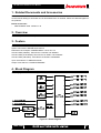
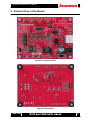
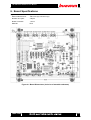
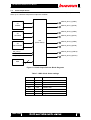
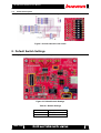
TB-SUB-CLK2 Hardware User Manual TB-SUB-CLK2 Hardware User Manual Rev.1.00 Rev.1.00 1 TB-SUB-CLK2 Hardware User Manual Revision History Version Date Description Publisher Rev.1.00 2012/05/02 Release version Yoshioka Rev.1.00 2 TB-SUB-CLK2 Hardware User Manual Table of Contents 1. 2. 3. 4. 5. 6. 7. 8. Related Documents and Accessories ......................................................................................... 8 Overview ...................................................................................................................................... 8 Feature ........................................................................................................................................ 8 Block Diagram ............................................................................................................................. 8 External View of the Board .......................................................................................................... 9 Board Specifications .................................................................................................................. 10 Description of Components ........................................................................................................11 7.1. Power supply ............................................................................................................................11 7.2. Power Input...............................................................................................................................11 7.3. Clock Input Select .................................................................................................................... 12 7.4. Clock Output Select ................................................................................................................. 13 7.5. Clock Select option .................................................................................................................. 14 Default Switch Settings ............................................................................................................. 14 Rev.1.00 3 TB-SUB-CLK2 Hardware User Manual List of Figures Figure 4-1 Block Diagram .................................................................................................................. 8 Figure 5-1 Component Side ............................................................................................................... 9 Figure 5-2 Solder Side ....................................................................................................................... 9 Figure 6-1 Board Dimensions (inclusive of wastable substrate) ...................................................... 10 Figure 7-1 Power Supply ...................................................................................................................11 Figure 7-2 Power Input ......................................................................................................................11 Figure 7-3 Input Clock Selector Block Diagram ............................................................................... 12 Figure 7-4 Clock Output Selector Block Diagrams .......................................................................... 13 Figure 7-5 CN12 external clock select ............................................................................................. 14 Figure 8-1 Default Switch Settings ................................................................................................... 14 List of Tables Table 7-1 SW3 Clock Select settings ............................................................................................... 13 Table 8-1 Default Settings ................................................................................................................ 14 Rev.1.00 4 TB-SUB-CLK2 Hardware User Manual Introduction Thank you for purchasing the TB-SUB-CLK2 board. Before using the product, be sure to carefully read this user manual and fully understand how to correctly use the product. First read through this manual, then always keep it handy. SAFETY PRECAUTIONS Be sure to observe these precautions Observe the precautions listed below to prevent injuries to you or other personnel or damage to property. Before using the product, read these safety precautions carefully to assure correct use. These precautions contain serious safety instructions that must be observed. After reading through this manual, be sure to always keep it handy. The following conventions are used to indicate the possibility of injury/damage and classify precautions if the product is handled incorrectly. Danger Indicates the high possibility of serious injury or death if the product is handled incorrectly. Indicates the possibility of serious injury or death if the product is handled Warning incorrectly. Indicates the possibility of injury or physical damage in connection with houses or Caution household goods if the product is handled incorrectly. The following graphical symbols are used to indicate and classify precautions in this manual. (Examples) Turn off the power switch. Do not disassemble the product. ! Rev.1.00 Do not attempt this. 5 TB-SUB-CLK2 Hardware User Manual Warning In the event of a failure, disconnect the power supply. If the product is used as is, a fire or electric shock may occur. Disconnect the power supply immediately and contact our sales personnel for repair. If an unpleasant smell or smoking occurs, disconnect the power supply. If the product is used as is, a fire or electric shock may occur. immediately. Disconnect the power supply After verifying that no smoking is observed, contact our sales personnel for repair. Do not disassemble, repair or modify the product. Otherwise, a fire or electric shock may occur due to a short circuit or heat generation. For inspection, modification or repair, contact our sales personnel. ! Do not touch a cooling fan. As a cooling fan rotates in high speed, do not put your hand close to it. cause injury to persons. ! Otherwise, it may Never touch a rotating cooling fan. Do not place the product on unstable locations. Otherwise, it may drop or fall, resulting in injury to persons or failure. ! If the product is dropped or damaged, do not use it as is. ! Do not touch the product with a metallic object. ! Do not place the product in dusty or humid locations or where water may Otherwise, a fire or electric shock may occur. Otherwise, a fire or electric shock may occur. splash. Otherwise, a fire or electric shock may occur. ! ! Do not get the product wet or touch it with a wet hand. Otherwise, the product may break down or it may cause a fire, smoking or electric shock. Do not touch a connector on the product (gold-plated portion). Otherwise, the surface of a connector may be contaminated with sweat or skin oil, resulting in contact failure of a connector or it may cause a malfunction, fire or electric shock due to static electricity. Rev.1.00 6 TB-SUB-CLK2 Hardware User Manual Caution Do not use or place the product in the following locations. ! Humid and dusty locations Airless locations such as closet or bookshelf Locations which receive oily smoke or steam Locations exposed to direct sunlight Locations close to heating equipment Closed inside of a car where the temperature becomes high Staticky locations Locations close to water or chemicals Otherwise, a fire, electric shock, accident or deformation may occur due to a short circuit or heat generation. ! Do not place heavy things on the product. Otherwise, the product may be damaged. ■ Disclaimer This product is a board intended for External Clock to FPGA evaluation boards. Tokyo Electron Device Limited assumes no responsibility for any damages resulting from the use of this product for purposes other than those stated. Even if the product is used properly, Tokyo Electron Device Limited assumes no responsibility for any damages caused by: (1) Earthquake, thunder, natural disaster or fire resulting from the use beyond our responsibility, acts by a third party or other accidents, the customer’s willful or accidental misuse or use under other abnormal conditions. (2) Secondary impact arising from use of this product or its unusable state (business interruption or others) (3) Use of this product against the instructions given in this manual. (4) Malfunctions due to connection to other devices. Tokyo Electron Device Limited assumes no responsibility or liability for: (1) Erasure or corruption of data arising from use of this product. (2) Any consequences or other abnormalities arising from use of this product, or (3) Damage of this product not due to our responsibility or failure due to modification This product has been developed by assuming its use for research, testing or evaluation. It is not authorized for use in any system or application that requires high reliability. Repair of this product is carried out by replacing it on a chargeable basis, not repairing the faulty devices. However, non-chargeable replacement is offered for initial failure if such notification is received within two weeks after delivery of the product. The specification of this product is subject to change without prior notice. The product is subject to discontinuation without prior notice. Rev.1.00 7 TB-SUB-CLK2 Hardware User Manual 1. Related Documents and Accessories Related documents: All documents relating to this board can be downloaded from our website. Please see attached paper on the products. Board accessories: - MMCX-MMCX cable: 1000mm x 10 2. Overview This board provides 4 clock outputs from onboard clock sources to MMCX connectors 3. Feature External differential clock input: SAMTEC MMCX-J-P-ST-TH1 x1 Option OSC socket: OMRON XR2A-0811-N Differential clock outputs: SAMTEC MMCX-J-P-ST-TH1 x4 Onboard OSC(135MHz): Tama Device CL20VBC 135.000MHz Onboard OSC(18.3516MHz): Tama Device CL20VBC 148.3516MHz Onboard OSC(148.5MHz): Tama Device CL20VBC 148.500MHz Input clock selector: TI SN65LVDS122D Output clock selector: TI SN65LVDS250DBT 4. Block Diagram Following figure shows a block diagram of TB-SUB-CLK2 Figure 4-1 Block Diagram Rev.1.00 8 TB-SUB-CLK2 Hardware User Manual 5. External View of the Board Following figures show external view of TB-SUB-CLK2 Figure 5-1 Component Side Figure 5-2 Solder Side Rev.1.00 9 TB-SUB-CLK2 Hardware User Manual 6. Board Specifications Figure 6-1 shows the board specifications. External Dimensions: 100.0 mm (W) x 80.0 mm (H) Number of Layers: 4 layers Board Thickness: 1.6 mm Material: FR-4 Figure 6-1 Board Dimensions (inclusive of wastable substrate) Rev.1.00 10 TB-SUB-CLK2 Hardware User Manual 7. Description of Components 7.1. Power supply Following figure shows the power supply structure Figure 7-1 Power Supply 7.2. Power Input This board has two Power connectors CN1 ATX connector and JACK1. SW1 is select switch for power input connector. If using AC Adaptor, SW1 is ON then if using ATX power supply, SW1 is OFF. Figure 7-2 Power Input Rev.1.00 11 TB-SUB-CLK2 Hardware User Manual 7.3. Clock Input Select This board has a MMCX connectors and OSC socket(DIP 8pins) for other required clock frequency. MMCX input signal level is LVDS at default settings. LVPECL signal is acceptable, if modified termination register. OSC socket is supported 3.3V OSC. SW2 is selector for MMCX or OSC. It can accept 2.5V OSC but It needs modified filter device. Please refer to TB-SUB-CLK2 schematic. MMCX_IN_P(CN2) OP_CLK_P MMCX_IN_P(CN3) IC5 (Clock Select) X4 IC5 (option OSC) (singl end =>LVDS) OP_CLK_N SW2 Figure 7-3 Input Clock Selector Block Diagram Rev.1.00 12 TB-SUB-CLK2 Hardware User Manual 7.4. Clock Output Select This board has 135MHz/148.3516MHz/148.5MHz of OSC and can be select frequency to MMXC by SW3. Up to 4 deferent frequencies output are available. MMCX_OUT1_P(CN4) X1 135MHz MMCX_OUT1_N(CN5) MMCX_OUT2_P(CN6) X2 148.5MHz MMCX_OUT2_N(CN7) IC6 (Clock Select) MMCX_OUT3_P(CN8) X3 148.3516MHz MMCX_OUT3_N(CN9) OP_CLK_P MMCX_OUT4_P(CN10) OP_CLK_N MMCX_OUT4_N(CN11) SW3 Figure 7-4 Clock Output Selector Block Diagrams Table 7-1 SW3 Clock Select settings Rev.1.00 1 2 MMCX1 P/N 3 4 MMCX2 P/N 5 6 MMCX3 P/N 7 8 MMXC4 P/N OFF OFF 135MHz P/N OFF ON 148.5MHz P/N ON OFF 148.3516MHz P/N ON ON OP_CLK P/N 13 TB-SUB-CLK2 Hardware User Manual 7.5. Clock Select option CN12(no mounted) is used for external clock select control. Signals level is 2.5V. Figure 7-5 CN12 external clock select 8. Default Switch Settings Following figure and table show default Switch settings Figure 8-1 Default Switch Settings Table 8-1 Default Settings Rev.1.00 SW1 1 (ATX) SW2 OFF (Option OSC) SW3 All OFF 14 TB-SUB-CLK2 Hardware User Manual PLD Solution Dept. PLD Division URL: http://solutions.inrevium.com/ E-mail: [email protected] HEAD Quarter: Yokohama East Square, 1-4 Kinko-cho, Kanagawa-ku, Yokohama City, Kanagawa, Japan 221-0056 TEL: +81-45-443-4016 FAX: +81-45-443-4058 Rev.1.00 15