1
VHDL Primer
A p p e n d ix A
VHDL Primer
A.1
VHDL Standards History. . . . . . . . . . . . . . . . . . . . . . . . . . . . . . . . . . . . . . . . . . . . . . . A-1
A.1.1 IEEE Standard 1076. . . . . . . . . . . . . . . . . . . . . . . . . . . . . . . . . . . . . . . . . . . . . A-1
A.1.2 IEEE Standard 1164. . . . . . . . . . . . . . . . . . . . . . . . . . . . . . . . . . . . . . . . . . . . . A-1
A.1.2.1IEEE Standard 1076.3 (Numeric Standard) . . . . . . . . . . . . . . . . . . . . . A-2
A.1.2.2IEEE Standard 1076.4 (VITAL). . . . . . . . . . . . . . . . . . . . . . . . . . . . . . . A-2
A.2
Learning VHDL . . . . . . . . . . . . . . . . . . . . . . . . . . . . . . . . . . . . . . . . . . . . . . . . . . . . . . A-3
A.2.1 A Simple Example . . . . . . . . . . . . . . . . . . . . . . . . . . . . . . . . . . . . . . . . . . . . . . A-3
A.2.2 Entity Declarations . . . . . . . . . . . . . . . . . . . . . . . . . . . . . . . . . . . . . . . . . . . . . . A-4
A.2.3 Architecture Declarations . . . . . . . . . . . . . . . . . . . . . . . . . . . . . . . . . . . . . . . . . A-5
A.2.4 Data Types . . . . . . . . . . . . . . . . . . . . . . . . . . . . . . . . . . . . . . . . . . . . . . . . . . . . A-6
A.2.5 Design Units . . . . . . . . . . . . . . . . . . . . . . . . . . . . . . . . . . . . . . . . . . . . . . . . . . . A-6
A.2.6 Levels of Abstraction . . . . . . . . . . . . . . . . . . . . . . . . . . . . . . . . . . . . . . . . . . . . A-9
A.2.6.1Sample Circuit . . . . . . . . . . . . . . . . . . . . . . . . . . . . . . . . . . . . . . . . . . A-10
A.2.6.2Comparator (Dataflow) . . . . . . . . . . . . . . . . . . . . . . . . . . . . . . . . . . . . A-11
A.2.6.3Barrel Shifter (Entity) . . . . . . . . . . . . . . . . . . . . . . . . . . . . . . . . . . . . . A-13
A.2.6.4Signals and Variables . . . . . . . . . . . . . . . . . . . . . . . . . . . . . . . . . . . . . A-17
A.2.6.5Using a Procedure . . . . . . . . . . . . . . . . . . . . . . . . . . . . . . . . . . . . . . . A-17
A.2.6.6Structural VHDL . . . . . . . . . . . . . . . . . . . . . . . . . . . . . . . . . . . . . . . . . A-19
A.2.6.7Design Hierarchy . . . . . . . . . . . . . . . . . . . . . . . . . . . . . . . . . . . . . . . . A-20
A.2.6.8Test Benches . . . . . . . . . . . . . . . . . . . . . . . . . . . . . . . . . . . . . . . . . . . A-21
A.2.6.9Sample Test Bench . . . . . . . . . . . . . . . . . . . . . . . . . . . . . . . . . . . . . . A-21
A.3
Conclusion . . . . . . . . . . . . . . . . . . . . . . . . . . . . . . . . . . . . . . . . . . . . . . . . . . . . . . . . A-23
A.4
Examples Gallery . . . . . . . . . . . . . . . . . . . . . . . . . . . . . . . . . . . . . . . . . . . . . . . . . . . A-23
A.4.1 Using Type Version Functions . . . . . . . . . . . . . . . . . . . . . . . . . . . . . . . . . . . . A-23
A.4.1.1Design Description . . . . . . . . . . . . . . . . . . . . . . . . . . . . . . . . . . . . . . . A-24
A.4.1.2Test Bench . . . . . . . . . . . . . . . . . . . . . . . . . . . . . . . . . . . . . . . . . . . . . A-26
A.4.2 Describing a State Machine . . . . . . . . . . . . . . . . . . . . . . . . . . . . . . . . . . . . . . A-27
A.4.2.1Design Description . . . . . . . . . . . . . . . . . . . . . . . . . . . . . . . . . . . . . . . A-27
A.4.2.2Test Bench . . . . . . . . . . . . . . . . . . . . . . . . . . . . . . . . . . . . . . . . . . . . . A-30
A.4.3 Reading and Writing from Files . . . . . . . . . . . . . . . . . . . . . . . . . . . . . . . . . . . A-32
Multisim User Guide
VDHL Prrimer
A.4.3.1Design Description. . . . . . . . . . . . . . . . . . . . . . . . . . . . . . . . . . . . . . . A-33
A.4.3.2Test Bench. . . . . . . . . . . . . . . . . . . . . . . . . . . . . . . . . . . . . . . . . . . . . A-34
Electronics Workbench
VHDL Primer
A p p e n d ix
A
VHDL Primer
This section provides a solid introduction to programming in VHDL. It is not intended to be a
fully comprehensive VHDL reference. It is made up of an overview of VHDL standards, a
section on learning VHDL, a conclusion and several examples.
A.1
VHDL Standards History
This section provides a detailed history of VHDL standards.
A.1.1 IEEE Standard 1076
In the early 1980s, a team of engineers from three companies — IBM, Texas Instruments and
Intermetrics — were contracted by the Department of Defense to complete the specification
and implementation of a new, language-based design description method. The first publicly
available version of VHDL, version 7.2, was released in 1985. In 1986, the Institute of Electrical and Electronics Engineers, Inc. (IEEE) was presented with a proposal to standardize the
language, which it did in 1987 after substantial enhancements and modifications were made
by a team of commercial, government and academic representatives. The resulting standard,
IEEE 1076-1987, is the basis for virtually every VHDL simulation and synthesis product sold
today. An enhanced and updated version of the language, IEEE 1076-1993, was released in
1994, and VHDL tool vendors have been responding by adding these new language features
to their products.
A.1.2 IEEE Standard 1164
Although IEEE Standard 1076 defines the complete VHDL language, there are aspects of the
language that make it difficult to write completely portable design descriptions (descriptions
that can be simulated identically using different vendors’ tools). The problem stems from the
Multisim User Guide
A-1
VDHL Prrimer
VHDL Primer
fact that VHDL supports many abstract data types, but it does not address the simple problem
of characterizing different signal strengths or commonly used simulation conditions such as
unknowns and high-impedance.
Soon after IEEE 1076-1987 was adopted, simulator companies began enhancing VHDL with
new signal types (typically through the use of syntactically legal, but nonstandard, enumerated types) to allow their customers to accurately simulate complex electronic circuits. This
caused problems because design descriptions entered using one simulator were often incompatible with other simulation environments. VHDL was quickly becoming nonstandard.
To get around the problem of nonstandard data types, another standard, numbered 1164, was
created by an IEEE committee. It defines a standard package (a VHDL feature that allows
commonly used declarations to be collected into an external library) containing definitions for
a standard nine-valued data type. This standard data type is called std_logic, and the IEEE
1164 package is often referred to as the standard logic package, or MVL9 (for multi-valued
logic, nine values).
The IEEE 1076-1987 and IEEE 1164 standards together form the VHDL standard in widest
use today. (IEEE 1076-1993 is slowly working its way into the VHDL mainstream, but it does
not add significant new features for synthesis users.)
A.1.2.1 IEEE Standard 1076.3 (Numeric Standard)
Standard 1076.3 (often called the Numeric Standard or Synthesis Standard) defines standard
packages and interpretations for VHDL data types as they relate to actual hardware. This standard is intended to replace the many custom (nonstandard) packages that vendors of synthesis
tools have created and distributed with their products.
IEEE Standard 1076.3 does for synthesis users what IEEE 1164 did for simulation users:
increase the power of Standard 1076, while at the same time ensuring compatibility between
different vendors’ tools. The 1076.3 standard includes, among other things:
•
•
•
A documented hardware interpretation of values belonging to the bit and boolean types
defined by IEEE Standard 1076, as well as interpretations of the std_ulogic type
defined by IEEE Standard 1164.
A function that provides “don’t care” or “wild card” testing of values based on the
std_ulogic type. This is of particular use for synthesis, since it is often helpful to
express logic in terms of “don’t care” values.
Definitions for standard signed and unsigned arithmetic data types, along with arithmetic,
shift, and type conversion operations for those types.
A.1.2.2 IEEE Standard 1076.4 (VITAL)
The annotation of timing information to a simulation model is an important aspect of accurate
digital simulation. The VHDL 1076 standard describes a variety of language features that can
A-2
Electronics Workbench
be used for timing annotation; however, it does not describe a standard method for expressing
timing data outside of the timing model itself.
The ability to separate the behavioral description of a simulation model from the timing specifications is important for many reasons. One of the major strengths of Verilog HDL is the fact
that it includes a feature specifically intended for timing annotation. This feature, the Standard
Delay Format (SDF), allows timing data to be expressed in a tabular form and included into
the Verilog timing model at the time of simulation.
The IEEE 1076.4 standard, published by the IEEE in late 1995, adds this capability to VHDL
as a standard package. A primary impetus behind this standard effort (which was dubbed
VITAL, for VHDL Initiative Toward ASIC Libraries) was to make it easier for ASIC vendors
and others to generate timing models applicable to both VHDL and Verilog HDL. For this reason, the underlying data formats of IEEE 1076.4 and Verilog’s SDF are quite similar.
A.2
Learning VHDL
This section presents several sample circuits and shows how they can be described for synthesis and testing. These small examples are not intended to represent real applications, but will
help you to understand the relationships between various types of VHDL statements and the
actual hardware being described.
In addition to the quick introduction to VHDL presented in this section, very important concepts such as concurrency and hierarchy will be introduced. Before explaining these more
complex topics, a very simple example will be presented so you can see what constitutes the
minimum VHDL source file.
A.2.1 A Simple Example
The following is a look at a very simple combinational circuit: an 8-bit comparator. This comparator will accept two 8-bit inputs, compare them, and produce a 1-bit result (either 1, indicating a match, or 0, indicating a difference between the two input values). A comparator such
as this is a combinational function constructed in circuitry from an arrangement of exclusiveOR gates or from some other lower-level structure depending on the capabilities of the target
technology. (It is the job of logic synthesis to determine exactly what hardware representation
is most appropriate for a given device.)
entity compare is
port(A,B: in bit;
EQ: out bit);
end compare;
architecture compare1 of compare is
Multisim User Guide
A-3
VHDL Primer
Learning VHDL
VDHL Prrimer
VHDL Primer
begin
EQ <= ‘1’ when (A = B) else ‘0’;
end compare1;
Reading from the top of the source file, you can see the following elements:
•
•
An entity declaration that defines the inputs and outputs — the ports — of this circuit.
An architecture declaration that defines what the circuit actually does, using a single concurrent assignment.
Every VHDL design description consists of the following:
1. At least one entity/architecture pair, which in VHDL jargon is sometimes referred to as a
“design entity”. In a large design, you will typically write many entity/architecture pairs
and connect them together to form a complete circuit.
An entity declaration describes the circuit as it appears from the “outside”, that is, from
the perspective of its input and output interfaces. If you are familiar with schematics, you
might think of the entity declaration as being analogous to a block symbol on a schematic.
2. The architecture declaration, which refers to the fact that every entity in a VHDL design
description must be bound with a corresponding architecture. The architecture describes
the actual function — or contents — of the entity to which it is bound.
A.2.2 Entity Declarations
An entity declaration provides the complete interface for a circuit. Using the information provided in an entity declaration (the names, data types and direction of each port), you have all
the information you need to connect that portion of a circuit into other, higher-level circuits,
or to develop input stimulus (in the form of a test bench) for testing purposes. The actual operation of the circuit, however, is not included in the entity declaration.
The following entity declaration contains a simple design description:
entity compare is
port( A, B: in bit_vector(0 to 7);
EQ: out bit);
end compare;
The entity declaration includes a name, compare, and port declaration statement defining all
the inputs and outputs of the entity. The port list includes definitions of three ports: A, B, and
EQ. Each of these three ports is given a direction (in, out or inout), and a type (in this case,
A-4
Electronics Workbench
either bit_vector(0 to 7), which specifies an 8-bit array, or bit, which represents a
single-bit value).
There are many different data types available in VHDL. To keep this introductory circuit simple, the simplest data types in VHDL, bit and bit_vector, will be used.
A.2.3 Architecture Declarations
Every entity declaration you write must be accompanied by at least one corresponding architecture.
The architecture declaration for the comparator circuit is as follows:
architecture compare1 of compare is
begin
EQ <= ‘1’ when (A = B) else ‘0’;
end compare1;
The architecture declaration begins with a unique name, “compare1”, followed by the name
of the entity to which the architecture is bound, in this case “compare”. Within the architecture declaration (between the begin and end keywords) is found the actual functional
description of our comparator. There are many ways to describe combinational logic functions
in VHDL; the method used in this simple design description is a type of concurrent statement
known as a conditional assignment. This assignment specifies that the value of the output
(EQ) will be assigned a value of ‘1’ when A and B are equal, and a value of ‘0’ when they differ.
This single concurrent assignment demonstrates the simplest form of a VHDL architecture.
There are many different types of concurrent statements available in VHDL, allowing you to
describe very complex architectures. Hierarchy and subprogram features of the language
allow you to include lower-level components, subroutines and functions in your architectures,
and a powerful statement known as a “process” allows you to describe complex sequential
logic as well.
Multisim User Guide
A-5
VHDL Primer
Learning VHDL
VDHL Prrimer
VHDL Primer
A.2.4 Data Types
Like a high-level software programming language, VHDL allows data to be represented in
terms of high-level data types. These data types can represent individual wires in a circuit, or
they can represent collections of wires using a concept called an “array”.
The preceding description of the comparator circuit used the data types bit and
bit_vector for its inputs and outputs. The bit data type has only two possible values: ‘1’
or ‘0’. (A bit_vector is simply an array of bits.) Every data type in VHDL has a defined
set of values, and a defined set of valid operations. Type checking is strict, so it is not possible, for example, to directly assign the value of an integer data type to a bit_vector data
type. (There are ways to get around this restriction, using what are called type conversion
functions. These are not discussed in this manual, but examples of their use are provided in
“A.4 Examples Gallery” on page A-23.
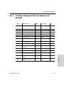
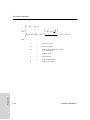
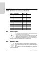
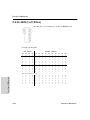
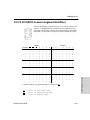
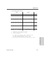
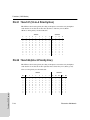
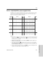
The following chart summarizes the fundamental data types available in VHDL.
Data Type
Values
Example
Bit
‘1’, ‘0’
Q <= ‘1’;
Bit_vector
(array of bits)
DataOut <= “00010101”;
Boolean
True, False
EQ <= True;
Integer
-2, -1, 0, 1, 2, 3, 4, etc.
Count <= Count + 2;
Real
1.0, -1.0E5, etc.
V1 = V2 / 5.3
Physical
1 ua, 7 ns, 100 ps, etc.
Q <= ‘1’ after 6 ns;
Record
(various)
Tvec := (Clk, Inp, Result);
Character
‘a’, ‘b’, ‘2, ‘$’, etc.
CharData <= ‘X’;
String
(Array of characters)
Msg <= “MEM: “ & Addr
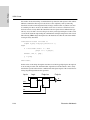
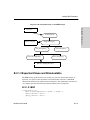
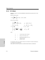
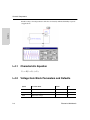
A.2.5 Design Units
One concept unique to VHDL (when compared to software programming languages and to
Verilog HDL) is the concept of a “design unit”. Design units (which may also be referred to as
“library units”) are segments of VHDL code that can be compiled separately and stored in a
library. You have been introduced to two design units already: the entity and the architecture.
There are actually five types of design units in VHDL: entities, architectures, packages, package bodies, and configurations.
A-6
Electronics Workbench
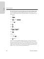
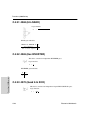
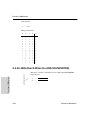
1. The diagram below illustrates the relationship of these five design units:
•
Entities
A VHDL entity is a statement (identified by the entity keyword) that defines the external specification of a circuit or sub-circuit. The minimum VHDL design description must
include at least one entity and one corresponding architecture.
When you write an entity declaration, you must provide a unique name for that entity and
a port list defining the input and output ports of the circuit. Each port in the port list must
be given a name, direction (or “mode”, in VHDL jargon) and a type. Optionally, you may
also include a special type of parameter list (called a generic list) that allows you to pass
additional information into an entity.
•
Architectures
A VHDL architecture declaration is a statement (beginning with the architecture
keyword) that describes the underlying function and/or structure of a circuit. Each architecture in your design must be associated (or bound) by name with one entity in the
design.
VHDL allows you to create more than one alternate architecture for each entity. This feature is particularly useful for simulation and for project team environments in which the
design of the system interfaces (expressed as entities) is done by a different engineer than
the lower-level architectural description of each component circuit.
An architecture declaration consists of zero or more declarations (of items such as intermediate signals, components that will be referenced in the architecture, local functions
Multisim User Guide
A-7
VHDL Primer
Learning VHDL
VDHL Prrimer
VHDL Primer
and procedures, and constants) followed by a begin statement, a series of concurrent
statements, and an end statement.
•
Packages and Package Bodies
A VHDL package declaration is identified by the package keyword, and is used to collect commonly-used declarations for use globally among different design units. You can
think of a package as a common storage area, one used to store such things as type declarations, constants, and global subprograms. Items defined within a package can be made
visible to any other design unit in the complete VHDL design, and they can be compiled
into libraries for later re-use.
A package can consist of two basic parts: a package declaration and an optional package
body. Package declarations can contain the following types of statements:
• type and subtype declarations
• constant declarations
• global signal declarations
• function and procedure declarations
• attribute specifications
• file declarations
• component declarations
• alias declarations
• disconnect specifications
• use clauses.
Items appearing within a package declaration can be made visible to other design units
through the use of a use statement, as will be shown.
If the package contains declarations of subprograms (functions or procedures) or defines
one or more deferred constants (constants whose value is not immediately given), then a
package body is required in addition to the package declaration. A package body (which is
specified using the package body keyword combination) must have the same name as
its corresponding package declaration, but it can be located anywhere in the design (it
does not have to be located immediately after the package declaration).
The relationship between a package and package body is somewhat akin to the relationship between an entity and its corresponding architecture. (There may be only one package body written for each package declaration, however.) While the package declaration
provides the information needed to use the items defined within it (the parameter list for a
global procedure, or the name of a defined type or subtype), the actual behavior of such
elements as procedures and functions must be specified within package bodies.
Examples of global procedures and functions can be found in “A.4 Examples Gallery” on
page A-23.
•
A-8
Configurations
Electronics Workbench
The final type of design unit available in VHDL is called a configuration declaration. A
configuration declaration (identified with the configuration keyword) specifies
which architectures are to be bound to which entities, and allows you to change how components are connected in your design description at the time of simulation or synthesis.
Configuration declarations are always optional, no matter how complex a design description you create. In the absence of a configuration declaration, the VHDL standard specifies a set of rules that provide you with a default configuration. For example, in the case
where you have provided more than one architecture for an entity, the last architecture
compiled will take precedence and will be bound to the entity.
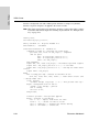
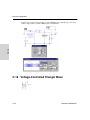
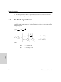
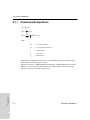
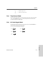
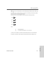
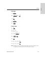
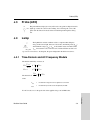
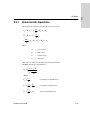
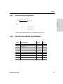
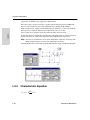
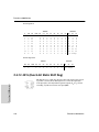
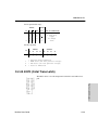
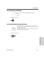
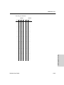
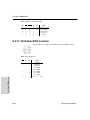
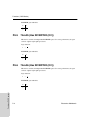
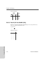
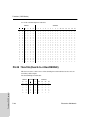
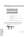
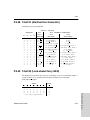
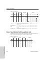
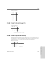
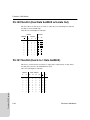
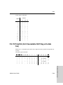
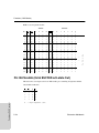
A.2.6 Levels of Abstraction
VHDL supports many possible styles of design description. These styles differ primarily in
how closely they relate to the underlying hardware. The different styles of VHDL refer to the
differing levels of abstraction possible using the language — behavior, dataflow, and structure
— as shown in the following diagram:
This figure maps the various points in a top-down design process to the three general levels of
abstraction. Starting at the top, suppose the performance specifications for a given project are:
“the compressed data coming out of the DSP chip needs to be analyzed and stored within 70
nanoseconds of the Strobe signal being asserted...” This human language specification must
be refined into a description that can actually be simulated. A test bench written in combination with a sequential description is one such expression of the design. These are all points in
the behavior level of abstraction.
After this initial simulation, the design must be further refined until the description is something a VHDL synthesis tool can digest. That is the dataflow level of abstraction.
The structure level of abstraction occurs when smaller segments of circuitry are being connected together to form a larger circuit. The structure level is commonly thought of as a circuit
netlist, or perhaps a higher-level block diagram.
The three levels of abstraction are as follows:
1. Behavior
The highest level of abstraction supported in VHDL is called the behavior level of abstraction. When creating a behavioral description of a circuit, you will describe your circuit in
terms of its operation over time. The concept of time is the critical distinction between
behavioral descriptions of circuits and lower-level descriptions (specifically descriptions
created at the dataflow level of abstraction).
In a behavioral description, the concept of time may be expressed precisely, with actual
delays between related events (such as the propagation delays within gates and on wires),
Multisim User Guide
A-9
VHDL Primer
Learning VHDL
VDHL Prrimer
VHDL Primer
or it may simply be an ordering of operations that are expressed sequentially (such as in a
functional description of a flip-flop). When you are writing VHDL for input to synthesis
tools, you may use behavioral statements to imply that there are registers in your circuit. It
is unlikely, however, that your synthesis tool will be capable of creating precisely the same
behavior in actual circuitry as you have defined in the language. (Synthesis tools today
ignore detailed timing specifications, leaving the actual timing results to the target device
technology.)
If you are familiar with event-driven software programming, writing behavior-level
VHDL will not seem like anything new. Just like with a programming language, you will
be writing one or more small programs that operate sequentially and communicate with
one another through their interfaces. The only difference between behavior-level VHDL
and a software programming language is the underlying execution platform: in the case of
software, it is some operating system running on a CPU; in the case of VHDL, it is the
simulator.
2. Dataflow
In the dataflow level of abstraction, you describe your circuit in terms of how data moves
through the system. At the heart of most digital systems today are registers, so in the dataflow level of abstraction you describe how information is passed between registers in the
circuit. You will probably describe the combinational logic portion of your circuit at a relatively high level (and let a synthesis tool figure out the detailed implementation in logic
gates), but you will likely be quite specific about the placement and operation of registers
in the complete circuit.
3. Structure
The third level of abstraction, structure, is used to describe a circuit in terms of its components. Structure can be used to create a very low-level description of a circuit (such as a
transistor-level description) or a very high-level description (such as a block diagram).
In a gate-level description of a circuit, for example, components such as basic logic gates
and flip-flops might be connected in some logical structure to create the circuit. This is
what is often called a netlist. For a higher-level circuit (one in which the components
being connected are larger functional blocks), structure might simply be used to segment
the design description into manageable parts.
Structure-level VHDL features such as components and configurations are very useful for
managing complexity. The use of components can dramatically improve your ability to
reuse elements of your designs, and they can make it possible to work using a top-down
design approach.
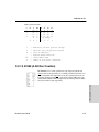
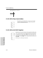
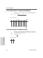
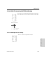
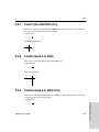
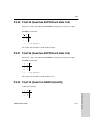
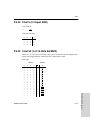
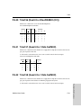
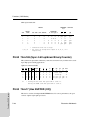
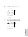
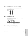
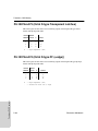
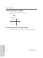
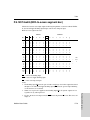
A.2.6.1 Sample Circuit
To help demonstrate some of the important concepts covered so far in this section, a very simple circuit will be presented. It will show how the function of this circuit can be described in
A-10
Electronics Workbench
VHDL. The design descriptions shown are intended for synthesis and therefore do not include
timing specifications or other information not directly applicable to today’s synthesis tools.
The circuit combines the comparator circuit presented in “A.2.1 A Simple Example” on page
A-3 with a simple 8-bit loadable shift register. The shift register will allow a detailed examination of how behavior-level VHDL can be written for synthesis.
The two subcircuits (the shifter and comparator) will be connected using VHDL’s hierarchy
features and will demonstrate the third level of abstraction: structure. The complete circuit is
shown below:
This diagram has been intentionally drawn to look like a hierarchical schematic with each of
the lower-level circuits represented as blocks. In fact, many of the concepts to be covered during the development of this circuit are familiar to users of schematic hierarchy. These concepts include the ideas of component instantiation, mapping of ports, and design partitioning.
In a more structured project environment, you would probably enter a circuit such as this by
first defining the interface requirements of each block, then describing the overall design of
the circuit as a collection of blocks connected together through hierarchy at the top level.
Later, after the system interfaces had been designed, you would proceed down the hierarchy
(using a top-down approach to design) and fill in the details of each subcircuit.
In this example, however, each of the lower-level blocks will be described and then they will
be connected to form the complete circuit.
A.2.6.2 Comparator (Dataflow)
The comparator portion of the design will be identical to the simple 8-bit comparator already
shown. The only difference is that the IEEE 1164 standard logic data types (std_ulogic
and std_ulogic_vector) will be used rather than the bit and bit_vector data types
used previously. Using standard logic data types for all system interfaces is highly recommended, as it allows circuit elements from different sources to be easily combined. It also provides you the opportunity to perform more detailed and precise simulation than would
otherwise be possible.
The updated comparator design, using the IEEE 1164 standard logic data types, is shown
below:
-------------------------------------- Eight-bit comparator
library ieee;
use ieee.std_logic_1164.all;
entity compare is
port (A, B: in std_ulogic_vector(0 to 7);
EQ: out std_ulogic);
Multisim User Guide
A-11
VHDL Primer
Learning VHDL
VDHL Prrimer
VHDL Primer
end compare;
architecture compare1 of compare is
begin
EQ <= ‘1’ when (A = B) else ‘0’;
end compare1;
Reading from the top of the source file, you can see the following:
•
•
•
•
•
a comment field, indicated by the leading double-dash symbol (“--”). VHDL allows comments to be embedded anywhere in your source file, provided they are prefaced by the two
hyphen characters as shown. Comments in VHDL extend from the double hyphen symbol
to the end of the current line. (There is no block comment facility in VHDL.)
a library statement that causes the named library IEEE to be loaded into the current
compile session. When you use VHDL libraries, it is recommended that you include your
library statements once at the beginning of the source file, before any use clauses or other
VHDL statements.
a use clause, specifying which items from the IEEE library are to be made visible for the
subsequent design unit (the entity and its corresponding architecture). The general form of
a use statement includes three fields delimited by a period: the library name (in this case
“ieee”), a design unit within the library (normally a package, in this case named
“std_logic_1164”), and the specific item within that design unit (or, as in this case, the
special keyword all, which means “everything”) to be made visible.
an entity declaration describing the interface to the comparator. Note that std_ulogic
and std_ulogic_vector, which are standard data types provided in the IEEE 1164
standard and in the associated IEEE library, were specified.
an architecture declaration describing the actual function of the comparator circuit.
Conditional Signal Assignment
The function of the comparator is defined using a simple concurrent assignment to port EQ.
The type of statement used in the assignment to EQ is called a “conditional signal assignment”. Conditional signal assignments make use of the “when-else” language feature and
allow complex conditional logic to be described. The following description of a multiplexer
circuit makes the use of the conditional signal assignment more clear:
architecture mux1 of mux is
begin
Y <=
A-12
A
B
C
D
when
when
when
when
(Sel
(Sel
(Sel
(Sel
=
=
=
=
“00”) else
“01”) else
“10”) else
“11”);
Electronics Workbench
end mux1;
Selected Signal Assignment
This form of signal assignment can be used as an alternative to the conditional signal assignment. The selected signal assignment has the following general form (again, using a multiplexer as an example):
architecture mux2 of mux is
begin
with Sel select
Y <=
A when
B when
C when
D when
end mux2;
“00”,
“01”,
“10”,
“11”;
Choosing between a conditional or selected signal assignment for circuits such as this is
largely a matter of taste. For most designs, there is no difference in the results obtained with
either type of assignment statement.
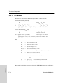
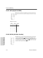
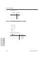
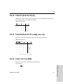
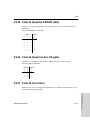
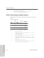
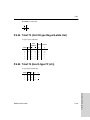
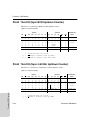
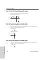
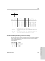
A.2.6.3 Barrel Shifter (Entity)
The second and most complex part of this design is the barrel shifter circuit. This circuit (diagrammed below) accepts 8-bit input data, loads this data into a register and, when the load
input signal is low, rotates this data by one bit with each rising edge clock signal. The circuit
is provided with an asynchronous reset, and the data stored in the register is accessible via the
output signal Q.
They are many ways to describe a circuit such as this in VHDL. If you are going to use synthesis tools to process the design description into an actual device technology, however, you
must restrict yourself to well established synthesis conventions when entering the circuit. Two
of these conventions will be looked at below.
Using a Process
The first design description to be looked at for this shifter is a description that uses a VHDL
process statement to describe the behavior of the entire circuit over time. This is the behavioral level of abstraction. It represents the highest level of abstraction practical (and synthesizable) for registered circuits such as this one. The VHDL source code for the barrel shifter is
shown below:
-----------------------------------------
Multisim User Guide
A-13
VHDL Primer
Learning VHDL
VDHL Prrimer
VHDL Primer
-- Eight-bit
barrel shifter
library ieee;
use ieee.std_logic_1164.all;
entity rotate is
port( Clk, Rst, Load: in std_ulogic;
Data: in std_ulogic_vector(0 to 7);
Q: out std_ulogic_vector(0 to 7));
end rotate;
architecture rotate1 of rotate is
begin
reg: process(Rst,Clk)
variable Qreg: std_ulogic_vector(0 to 7);
begin
if Rst = ‘1’ then
-- Async reset
Qreg := “00000000”;
elsif (Clk = ‘1’ and Clk’event) then
if (Load = ‘1’) then
Qreg := Data;
else
Qreg := Qreg(1 to 7) & Qreg(0);
end if;
end if;
Q <= Qreg;
end process;
end rotate1;
Reading from the top of the source file, you can see the following:
•
•
•
•
a comment field, as described previously.
library and use statements, allowing us to use the IEEE 1164 standard logic data
types.
an entity declaration defining the interface to the circuit. Note that the direction (mode) of
Q is written as out, indicating that it will not be used directly as the lower-level storage
object (Q will not be fed back directly).
an architecture declaration, consisting of a single process statement that defines the operation of the shifter over time in response to events appearing on the clock (Clk) and asynchronous reset (Rst).
Process Statement
The process statement in VHDL is the primary means by which sequential operations (such as
registered circuits) can be described. When describing registered circuits, the most common
form of a process statement is:
A-14
Electronics Workbench
architecture arch_name of ent_name is
begin
process_name: process(sensitivity_list)
local_declaration;
local_declaration;
. . .
begin
sequential statement;
sequential statement;
sequential statement;
.
.
.
end process;
end arch_name;
A process statement consists of the following items:
•
•
•
An optional process name (an identifier followed by a colon).
The process keyword.
An optional sensitivity list, indicating which signals result in the process “executing”
when there is some event detected. (The sensitivity list is required if the process does not
include one or more wait statements to suspend its execution at certain points. An example that does not use a sensitivity list is discussed in “A.2.6.5 Using a Procedure” on page
A-17.
• An optional declarations section, allowing local objects and subprograms to be defined.
• A begin keyword.
• A sequence of statements to be executed when the program runs.
• An end statement.
The easiest way to think of a VHDL process such as this is to relate it to software, as a program that executes (in simulation) any time there is an event on one of its inputs (as specified
in the sensitivity list). A process describes the sequential execution of statements that are
dependent on one or more events occurring. A flip-flop is a perfect example of such a situation; it remains idle, not changing state, until there is a significant event (either a rising edge
on the clock input or an asynchronous reset event) that causes it to operate and potentially
change its state.
Although there is a definite order of operations within a process (from top to bottom), you can
think of a process as executing in zero time. This means that (a) a process can be used to
describe circuits functionally, without regard to their actual timing, and (b) multiple processes
can be “executed” in parallel with little or no concern for which processes complete their
Multisim User Guide
A-15
VHDL Primer
Learning VHDL
VDHL Prrimer
VHDL Primer
operations first. (There are certain caveats to this behavior of VHDL processes. These caveats
are described in detail in most VHDL textbooks.)
For your reference, the process of how the barrel shifter operates is shown below:
reg: process(Rst,Clk)
variable Qreg: std_ulogic_vector(0 to 7);
begin
if Rst = ‘1’ then
-- Async reset
Qreg := “00000000”;
elsif (Clk = ‘1’ and Clk’event) then
if (Load = ‘1’) then
Qreg := Data;
else
Qreg := Qreg(1 to 7) & Qreg(0);
end if;
end if;
Q <= Qreg;
end process;
As written, the process is dependent on (or sensitive to) the asynchronous inputs Rst and Clk.
These are the only signals that can have events directly affecting the operation of the circuit;
in the absence of any event on either of these signals, the circuit described by the process will
simply hold its current value (that is, the process will remain suspended).
Consider what happens when an event occurs on either one of these asynchronous inputs.
First, look at what happens when the input Rst has an event in which it transitions to a high
state (represented by the std_ulogic value of ‘1’). In this case, the process will begin execution and the first if statement will be evaluated. Because the event was a transition to ‘1’,
the simulator will see that the specified condition (Rst = ‘1’) is true and the assignment of
variable Qreg to the reset value of “00000000” will be performed. The remaining statements
of the if-then-elsif expression (those that are dependent on the elsif condition) will be
ignored. The final statement in the process, the assignment of output signal Q to the value of
Qreg, is not subject to the if-then-elsif expression and is therefore placed on the process queue
for execution. (Signal assignments do not occur until the process actually suspends.) Finally,
the process suspends, all signals that were assigned values in the process (in this case Q) are
updated, and the process waits for another event on Clk or Rst.
What about the case in which there is an event on Clk? In this case, the process will again execute, and the if-then-elsif expressions will be evaluated in turn until a valid condition is
encountered. If the Rst input continues to have a high value (a value of ‘1’), then the simulator
will evaluate the first if test as true, and the reset condition will take priority. If, however, the
Rst input is not a value of ‘1’, then the next expression (Clk = ‘1’ and Clk’event) will be
evaluated. This expression is the most commonly-used convention for detecting clock edges
A-16
Electronics Workbench
in VHDL. To detect a rising edge clock, write the expression Clk = ‘1’ in the conditional
expression. For this circuit, however, the expression Clk = ‘1’ would not be specific enough,
since the process may have begun execution as the result of an event on Rst that did not result
in Rst transitioning to a ‘1’. (For example, a falling edge event on Rst — that is, a transition
from 1 to 0 — would trigger the process but cause it to skip to the elsif statement even though
there was no event on Clk, since the Rst = 1 condition would evaluate as false.) To ensure that
the event we are responding to is in fact an event on Clk, we use the built-in VHDL attribute
‘event’ to check if Clk was the signal triggering the process execution.
If the event that triggered the process execution was in fact a rising edge on Clk, then the simulator will go on to check the remaining if-then logic to determine which assignment statement is to be executed. If Load is determined to be ‘1’, then the first assignment statement is
executed and the data is loaded from input data to the registers. If Load is not ‘1’, then the
data in the registers is shifted, as specified using the bit slice and concatenation operations
available in the language.
Note Every assignment to a variable or signal you make that is dependent on a Clk = ‘1’ and
Clk’event expression will result in at least one register when synthesized.
A.2.6.4 Signals and Variables
There are two fundamental types of objects used to carry data from place to place in a VHDL
design description: signals and variables. In virtually all cases, you will want to use variables
to carry data between sequential operations (within processes, procedures and functions) and
use signals to carry information between concurrent elements of your design (such as between
two independent processes).
Examples of signals and variables, and differences between them, are shown in more detail in
“A.4 Examples Gallery” on page A-23. For now, it is useful to think of signals as wires (as in
a schematic) and variables as temporary storage areas (similar to variables in a traditional
software programming language).
In many cases, you can choose whether to use signals or variables to perform the same task.
As a general rule, you should use variables whenever possible and use signals only when you
must access data across different concurrent parts of your design.
A.2.6.5 Using a Procedure
Describing registered logic using processes requires that you follow some established conventions (if you intend to synthesize the design) and to consider the behavior of the entire circuit.
In the barrel shifter design description shown in “Process Statement” on page A-14, the registers were implied by the placement and use of statements such as if Clk = ‘1’ and Clk’event.
Assignment statements subject to that clause resulted in D-type flip-flops being implied for
the signals.
Multisim User Guide
A-17
VHDL Primer
Learning VHDL
VDHL Prrimer
VHDL Primer
For smaller circuits, this mixing of combinational logic functions and registers is fine and not
difficult to understand. For larger circuits, however, the complexity of the system being
described can make such descriptions hard to manage, and the results of synthesis can often
be confusing. For these circuits, it often makes more sense to retreat to a dataflow level of
abstraction and to clearly define the boundaries between registered and combinational logic.
One easy way to do this is to remove the process from your design and replace it with a series
of concurrent statements representing the combinational and registered portions of the circuit.
The following VHDL design description uses this method to describe the same barrel shifter
circuit previously described:
architecture rotate3 of rotate is
signal D,Qreg: std_logic_vector(0 to 7);
begin
D <= Data when (Load = ‘1’) else
Qreg(1 to 7) & Qreg(0);
dff(Rst, Clk, D, Qreg);
Q <= Qreg;
end rotate3;
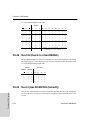
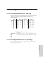
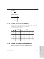
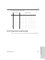
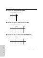
In this version of the design description, the behavior of the D-type flip-flop has been placed
in an external procedure, dff, and intermediate signals have been introduced to more clearly
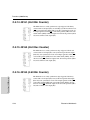
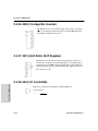
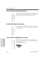
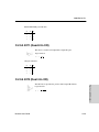
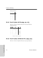
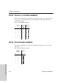
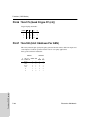
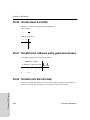
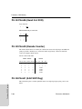
describe the separation between the combinational and registered parts of the circuit. The following diagram helps illustrate this separation:
Inputs
Logic
Registers
D
Outputs
Qreg
Q
Data
Load
Clk
Rst
A-18
Electronics Workbench
In this example, the combinational logic of the counter has been written in the form of a single
concurrent signal assignment, while the registered operation of the counter’s output has been
described using a call to a procedure named dff.
What does the dff procedure look like? The following is one possible procedure for a D-type
flip-flop:
procedure dff (signal Rst, Clk: in std_ulogic;
signal D: in std_ulogic_vector(0 to 7);
signal Q: out std_ulogic_vector(0 to 7)) is
begin
if Rst = ‘1’ then
Q <= “00000000”;
elsif Clk = ‘1’ and Clk’event then
Q <= D;
end if;
end dff;
Notice that this procedure has a striking resemblance to the process statement presented earlier. The same if-then-elsif structure used in the process is used to describe the behavior of the
registers. Instead of a sensitivity list, however, the procedure has a parameter list describing
the inputs and outputs of the procedure.
The parameters defined within a procedure or function definition are called its formal parameters. When the procedure or function is executed in simulation, the formal parameters are
replaced by the values of the actual parameters specified when the procedure or function is
used. If the actual parameters being passed into the procedure or function are signal objects,
then the signal keyword can be used (as shown above) to ensure that all information about the
signal object, including its value and all of its attributes, is passed into the procedure or function.
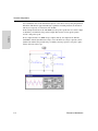
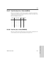
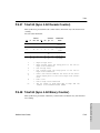
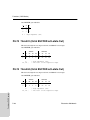
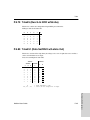
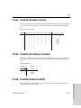
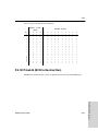
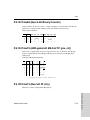
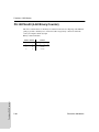
A.2.6.6 Structural VHDL
The structure level of abstraction is used to combine multiple components to form a larger circuit or system. As such, structure can be used to help manage a large and complex design, and
structure can make it possible to reuse components of a system in other design projects.
Because structure only defines the interconnections between components, it cannot be used to
completely describe the function of a circuit; at some level, all aspects of your circuit must be
described using behavioral and/or dataflow levels of abstraction.
To demonstrate how the structure level of abstraction can be used to connect lower-level circuit elements into a larger circuit, the comparator and shift register circuits will be connected
into a larger circuit as shown below.
Multisim User Guide
A-19
VHDL Primer
Learning VHDL
VDHL Prrimer
VHDL Primer
Note This diagram was drawn in much the same way you might enter it into Multisim.
Structural VHDL has many similarities with schematic-based design.
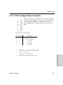
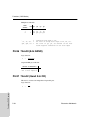
A.2.6.7 Design Hierarchy
When you write structural VHDL, you are in essence writing a textual description of a schematic netlist (a description of how the components on the schematic are connected by wires,
or nets). In the world of schematic entry tools, such netlists are usually created for you automatically by the schematic editor, as Multisim does. When writing VHDL, you enter the same
sort of information by hand.
When you use components and wires (signals, in VHDL) to connect multiple circuit elements
together, it is useful to think of your new, larger circuit in terms of a hierarchy of components.
In this view, the top-level drawing (or top-level VHDL entity and architecture) can be seen as
the highest level in a hierarchy tree, as shown below.
library ieee;
use ieee.std_logic_1164.all;
entity rotcomp is port(Clk, Rst, Load: in std_ulogic;
Init: in
std_ulogic_vector(0 to 7);
Test: in
std_ulogic_vector(0 to 7);
Limit: out std_ulogic);
end rotcomp;
architecture structure of rotcomp is
component compare
port(A, B: in std_ulogic_vector(0 to 7); EQ: out
std_ulogic);
end component;
component rotate
port(Clk, Rst, Load: in std_ulogic;
Data: in std_ulogic_vector(0 to 7);
Q: out std_ulogic_vector(0 to 7));
end component;
signal Q: std_ulogic_vector(0 to 7);
begin
COMP1: compare port map (A=>Q, B=>Test, EQ=>Limit);
A-20
Electronics Workbench
ROT1: rotate port map (Clk=>Clk, Rst=>Rst, Load=>Load,
Data=>Init, Q=>Q);
end structure;
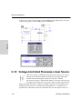
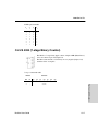
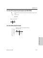
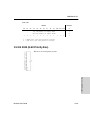
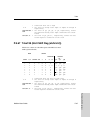
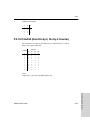
A.2.6.8 Test Benches
At this point, the sample circuit is complete and ready to be processed by synthesis tools.
Before processing the design, however, you should take the time to verify that it actually does
what it is intended to do. You should run a simulation.
Simulating a circuit such as this one requires that you provide more than just the design
description itself. To verify the proper operation of the circuit over time in response to input
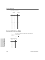
stimulus, you will need to write a test bench.
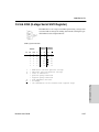
The easiest way to understand the concept of a test bench is to think of it as a virtual tester circuit. This tester circuit, which you will describe in VHDL, applies stimulus to your design
description and (optionally) verifies that the simulated circuit does what it is intended to do.
The diagram below graphically illustrates the relationship between the test bench and your
design description, which is called the unit under test, or UUT.
To apply stimulus to your design, your test bench will probably be written using one or more
sequential processes, and it will use a series of signal assignments and wait statements to
describe the actual stimulus. You will probably use VHDL’s looping features to simplify the
description of repetitive stimulus (such as the system clock), and you may also use VHDL’s
file and record features to apply stimulus in the form of test vectors.
To check the results of simulation, you will probably make use of VHDL’s assert feature, and
you may also use the file features to write the simulation results to a disk file for later analysis.
For complex design descriptions, developing a comprehensive test bench can be a large-scale
project in itself. In fact, it is not unusual for the test bench to be larger and more complex than
the design description. For this reason, you should plan your project so that you have the time
required to develop the function test in addition to developing the circuit being tested. You
should also plan to create test benches that are re-usable, perhaps by developing a master test
bench that reads test data from a file.
When you create a test bench for your design, you use the structural level of abstraction to
connect your lower-level (previously top-level) design description to the other parts of the test
bench.
A.2.6.9 Sample Test Bench
The following VHDL source statements describe a simple test bench for the shift and compare circuit. This test bench uses two processes that operate concurrently. One process (clock)
Multisim User Guide
A-21
VHDL Primer
Learning VHDL
VDHL Prrimer
VHDL Primer
describes a background clock with a 100 ns period, while the second process (stimulus)
describes a sequence of inputs to be applied to the circuit over time.
Note This sample test bench does not include any checking of output values. More complex
test benches that include output value checking are presented in “A.4 Examples Gallery” on page A-23.
library ieee;
use ieee.std_logic_1164.all;
entity testbnch is-- No ports needed in a
end testbnch;-- testbench
architecture behavior of testbnch is
component rotcomp is-- Declares the lower-level
port(Clk, Rst, Load: in std_ulogic;-- component
and its ports
Init: in std_ulogic_vector(0 to 7);
Test: in std_ulogic_vector(0 to 7);
Limit: out std_ulogic);
end component;
signal Clk, Rst, Load: std_ulogic;-- Introduces top-level signals
signal Init: std_ulogic_vector(0 to 7);-- to use when
signal Test: std_ulogic_vector(0 to 7);-- testing the lower-level
circuit
signal Limit: std_ulogic;
begin
DUT: rotcomp port map-- Creates an instance of the
(Clk, Rst, Load, Init, Test, Limit);-- lower-level circuit (the
-- design under test)
clock: process
variable clktmp: std_ulogic := ‘0’;-- This process sets up a
begin-- background clock of 100 ns
clktmp := not clktmp;-- period.
Clk <= clktmp;
wait for 50 ns;
end process;
stimulus: process-- This process applies
begin-- stimulus to the design
Rst <= ‘0’;-- inputs, then waits for some
Load <= ‘1’;-- amount of time so we can
Init <= “00001111”;-- observe the results during
Test <= “11110000”;-- simulation.
A-22
Electronics Workbench
wait for 100 ns;
Load <= ‘0’;
wait for 600 ns;
end process;
end behavior;
A.3
Conclusion
In this section the most important concepts and features of VHDL were explored. We hope
this introduction was a useful refresher for experienced VHDL users, and a good introduction
to the language for the novice. VHDL is a rich and powerful language, however, and there is
much more to learn before you become a “master user”. To continue your learning, it is
strongly recommended that you acquire at least one textbook on VHDL, and also obtain a
copy of the IEEE 1076 VHDL Language Reference Manual. There are also many good quality VHDL training courses and multimedia training products available. Contact Electronics
Workbench, or visit their Web page at www.interactiv.com for more information.
You will also find it useful to study, copy and modify existing VHDL design examples. “A.4
Examples Gallery” on page A-23 includes listings and descriptions of sample designs, and
additional examples are provided on your Multisim’s VHDL installation CD-ROM.
A.4
Examples Gallery
The examples in this section are intended to help you get started with VHDL. Each example
demonstrates one or more important features of the language, and demonstrates commonly
used coding styles for synthesizable circuits and test benches. These examples, and more, can
be found in the \EXAMPLES folder of your VHDL installation. You are encouraged to copy
these examples and modify them for your own use.
A.4.1 Using Type Version Functions
This example, an 8-bit counter, demonstrates one possible approach to type conversion. Type
conversions are often required in VHDL due to the languages’ strict type-checking features.
In this example, a type conversion is required to convert the array data types used in the
design’s interface to integer data types used internally for arithmetic operations. For demonstration purposes, we are using a custom type conversion function that is defined in the design
description. In most cases, you will want to use a standard type conversion function from the
IEEE library, or use a type conversion function provided by your synthesis vendor.
Multisim User Guide
A-23
VHDL Primer
Conclusion
VDHL Prrimer
VHDL Primer
Note Another option when numeric values are required is to make use of the IEEE 1076.3
numeric_std package. This package is provided in the library IEEE supplied with the
Multisim VHDL simulator.
A.4.1.1 Design Description
library ieee;
use ieee.std_logic_1164.all;
package conversions is
function to_unsigned (a: std_ulogic_vector) returninteger;
function to_vector (size: integer; num: integer) return
std_ulogic_vector;
end conversions;
package body conversions is
-------------------------------------------------------- Convert a std_ulogic_vector to an unsigned integer -function to_unsigned (a: std_ulogic_vector) return integer is
alias av: std_ulogic_vector (1 to a'length)is a;
variable ret,d: integer;
begin
d := 1;
ret := 0;
for i in a'length downto 1 loop
if (av(i) = '1') then
ret := ret + d;
end if;
d := d * 2;
end loop;
return ret;
end to_unsigned;
---------------------------------------------------- Convert an integer to a std_ulogic_vector -function to_vector (size: integer; num: integer) return
std_ulogic_vector is
variable ret: std_ulogic_vector (1 to size);
variable a: integer;
begin
a := num;
for i in size downto 1 loop
if ((a mod 2) = 1) then
ret(i) := '1';
A-24
Electronics Workbench
else
ret(i) := '0';
end if;
a := a / 2;
end loop;
return ret;
end to_vector;
end conversions;
-------------------------------------------------------- COUNT16: 4-bit counter.-Library ieee;
Use ieee.std_logic_1164.all;
use work.conversions.all;
Entity COUNT16 Is
Port (Clk,Rst,Load: in std_ulogic;
Data: in std_ulogic_vector(3 downto 0);
Count: out std_ulogic_vector(3 downto 0)
);
End COUNT16;
Architecture COUNT16_A of COUNT16 Is
Begin
process(Rst,Clk)
-- Note the use of a variable to localize the feedback behavior of the
counter registers. This is good general design practice in VHDL, as it
helps to cut down on unwanted side-effects. In this example, the use
of a variable of type integer also localizes the use of a numeric data
type to within the process itself. This makes it easier to modify the
design as necessary when using different type conversion routines.
variable Q: integer range 0 to 15;
begin
if Rst = '1' then
-- Asynchronous reset
Q := 0;
elsif rising_edge(Clk) then
if Load = '1' then
Q := to_unsigned(Data); -- Convert vector to integer
elsif Q = 15 then
Q := 0;
else
Multisim User Guide
A-25
VHDL Primer
Examples Gallery
VDHL Prrimer
VHDL Primer
Q := Q + 1;
end if;
end if;
Count <= to_vector(4,Q);
-- Convert integer to vector for use outside the process.
end process;
End COUNT16_A;
A.4.1.2 Test Bench
library ieee;
Use ieee.std_logic_1164.all;
Entity T_COUNT16 Is
End T_COUNT16;
use work.count16;
Architecture stimulus of T_COUNT16 Is
Component COUNT16
Port (Clk,Rst,Load: in std_ulogic;
Data: in std_ulogic_vector(3 downto 0);
Count: out std_ulogic_vector(3 downto 0)
);
End Component;
Signal Clk,Rst,Load: std_ulogic; -- Top level signals
Signal Data: std_ulogic_vector(3 downto 0);
Signal Count: std_ulogic_vector(3 downto 0);
Signal Clock_cycle: natural := 0;
Begin
DUT: COUNT16 Port Map (Clk,Rst,Load,Data,Count);
-- The first process sets up a 20Mhz background clock
CLOCK: process
begin
Clock_cycle <= Clock_cycle + 1;
Clk <= '1';
wait for 25 ns;
Clk <= '0';
wait for 25 ns;
A-26
Electronics Workbench
end process;
-- This process applies stimulus to reset and load the counter...
Stimulus1: Process
Begin
Rst <= '1';
wait for 40 ns;
Rst <= '0';
Load <= '1';
Data <= "0100";
-- Load 0100 into the counter
wait for 50 ns;
Load <= '0';
wait for 500 ns;
Load <= '1';
Data <= "0000";
-- Load 0000 into the counter
wait for 50 ns;
Load <= '0';
wait for 11000 ns;
wait;
End Process;
End stimulus;
A.4.2 Describing a State Machine
This example demonstrates how to write a synthesizable state machine description using processes and enumerated types.
The circuit, a video frame grabber controller, was first described in Practical Design Using
Programmable Logic by David Pellerin and Michael Holley (Prentice Hall, 1990). A slightly
modified form of the circuit also appears in the ATMEL Configurable Logic Design and
Application Book, 1993-1994 edition.
The circuit described is a simple freeze-frame unit that 'grabs' and holds a single frame of
NTSC color video image. This design description includes the frame detection and capture
logic. The complete circuit requires an 8-bit D-A/A-D converter and a 256K X 8 static RAM.
A.4.2.1 Design Description
-------------------------------------------------------- A Video Frame Grabber. -Library ieee;
Use ieee.std_logic_1164.all;
Multisim User Guide
A-27
VHDL Primer
Examples Gallery
VDHL Prrimer
VHDL Primer
Entity CONTROL Is
Port (Reset: in std_ulogic;
Clk: in std_ulogic;
Mode: in std_ulogic;
Data: in std_ulogic_vector(7 downto 0);
TestLoad: in std_ulogic;
Addr: out integer range 0 to 253243;
RAMWE: out std_ulogic;
RAMOE: out std_ulogic;
ADOE: out std_ulogic );
End CONTROL;
Architecture CONTROL_A of CONTROL Is
constant FRAMESIZE: integer := 253243;
constant TESTADDR: integer := 253000;
signal ENDFR: std_ulogic;
signal INCAD: std_ulogic;
signal VS: std_ulogic;
signal Sync: integer range 0 to 127;
type states is (StateLive,StateWait,StateSample,StateDisplay);
signal current_state, next_state: states;
Begin
-- Address counter. This counter increments until we reach the end of
the frame (address 253243), or until the input INCAD goes low.
ADDRCTR: process(Clk)
variable cnt: integer range 0 to FRAMESIZE;
begin
if rising_edge(Clk) then
if TestLoad = '1' then
cnt := TESTADDR;
ENDFR <= '0';
else
if INCAD = '0' or cnt = FRAMESIZE then
cnt := 0;
else
cnt := cnt + 1;
end if;
if cnt = FRAMESIZE then
ENDFR <= '1';
else
ENDFR <= '0';
end if;
A-28
Electronics Workbench
end if;
end if;
Addr <= cnt;
end process;
-- Vertical sync detector. Here we look for 128 bits of zero, which
indicates the vertical sync blanking interval.
SYNCCTR: process(Reset,Clk)
begin
if Reset = '1' then
Sync <= 0;
elsif rising_edge(Clk) then
if Data /= "00000000" or Sync = 127 then
Sync <= 0;
else
Sync <= Sync + 1;
end if;
end if;
end process;
VS <= '1' when Sync = 127 else '0';
-- State register process:
STREG: process(Reset,Clk)
begin
if Reset = '1' then
current_state <= StateLive;
elsif rising_edge(Clk) then
current_state <= next_state;
end if;
end process;
-- State transitions:
STTRANS: process(current_state,Mode,VS,ENDFR)
begin
case current_state is
when StateLive => -- Display live video on the output
RAMWE <= '1';
RAMOE <= '1';
ADOE <= '0';
INCAD <= '0';
Multisim User Guide
A-29
VHDL Primer
Examples Gallery
VDHL Prrimer
VHDL Primer
if Mode = '1' then
next_state <= StateWait;
end if;
when StateWait =>
-- Wait for vertical sync
RAMWE <= '1';
RAMOE <= '1';
ADOE <= '0';
INCAD <= '0';
if VS = '1' then
next_state <= StateSample;
end if;
when StateSample => -- Sample one frame of video
RAMWE <= '0';
RAMOE <= '1';
ADOE <= '0';
INCAD <= '1';
if ENDFR = '1' then
next_state <= StateDisplay;
end if;
when StateDisplay => -- Display the stored frame
RAMWE <= '1';
RAMOE <= '0';
ADOE <= '1';
INCAD <= '1';
if Mode = '1' then
next_state <= StateLive;
end if;
end case;
end process;
End CONTROL_A;
A.4.2.2 Test Bench
The following test bench uses loops to simplify the description of a long test sequence:
library ieee;
Use ieee.std_logic_1164.all;
Use std.textio.all;
library work;
use work.control;
Entity T_CONTROL Is
A-30
Electronics Workbench
End T_CONTROL;
Architecture stimulus of T_CONTROL Is
Component CONTROL
Port (Reset: in std_ulogic;
Clk: in std_ulogic;
Mode: in std_ulogic;
Data: in std_ulogic_vector(7 downto 0);
TestLoad: in std_ulogic;
Addr: out integer range 0 to 253243;
RAMWE: out std_ulogic;
RAMOE: out std_ulogic;
ADOE: out std_ulogic);
End Component;
Constant PERIOD: time := 100 ns;
-- Top level signals go here...
Signal Reset: std_ulogic;
Signal Clk: std_ulogic;
Signal Mode: std_ulogic;
Signal Data: std_ulogic_vector(7 downto 0);
Signal TestLoad: std_ulogic;
Signal Addr: integer range 0 to 253243;
Signal RAMWE: std_ulogic;
Signal RAMOE: std_ulogic;
Signal ADOE: std_ulogic;
Signal done: boolean := false;
Begin
DUT: CONTROL Port Map (
Reset => Reset,
Clk => Clk,
Mode => Mode,
Data => Data,
TestLoad => TestLoad,
Addr => Addr,
RAMWE => RAMWE,
RAMOE => RAMOE,
ADOE => ADOE
);
Clock1: process
variable clktmp: std_ulogic := '0';
begin
wait for PERIOD/2;
clktmp := not clktmp;
Clk <= clktmp; -- Attach your clock here
Multisim User Guide
A-31
VHDL Primer
Examples Gallery
VDHL Prrimer
VHDL Primer
if done = true then
wait;
end if;
end process;
Stimulus1: Process
Begin
-- Sequential stimulus goes here...
Reset <= '1';
Mode <= '0';
Data <= "00000000";
TestLoad <= '0';
wait for PERIOD;
Reset <= '0';
wait for PERIOD;
Data <= "00000001";
wait for PERIOD;
Mode <= '1';
-- Check to make sure we detect the vertical sync...
Data <= "00000000";
for i in 0 to 127 loop
wait for PERIOD;
end loop;
-- Now sample data to make sure the frame counter works...
Data <= "01010101";
for i in 0 to 100000 loop
wait for PERIOD;
end loop;
-- Load in the test value to check the end of frame detection...
TestLoad <= '1';
wait for PERIOD;
TestLoad <= '0';
for i in 0 to 300 loop
wait for PERIOD;
end loop;
done <= true;
End Process;
End stimulus;
A-32
Electronics Workbench
A.4.3 Reading and Writing from Files
More complex test benches often make use of VHDL’s file read and write capabilities. These
features make it easy to create test benches that operate on data stored in files, such as test
vectors. The following example demonstrates how you can use the text I/O features of VHDL
to read test data from an ASCII file.
Consider a Fibonacci sequence generator. A Fibonnaci sequence is a series of numbers, beginning with 1, 1, 2, 3, 5..., in which every number in the sequence is the sum of the previous two
numbers. To construct a circuit that generates an n-bit Fibonacci sequence, two n-bit registers
— A and B — are required to store the last two values of the sequence and add them to produce the next value.
To initialize the circuit, the A and B registers must be loaded with values of 0 and 1 respectively. Subsequent cycles of the circuit must move the calculated next value into the B register
while moving the value stored in the B register to the A register. In this implementation, the A
and B registers form a 2-deep first-in first-out (FIFO) stack.
The VHDL source file shown below describes this Fibonnaci sequence generator.
A.4.3.1 Design Description
------------------------------------------------------- Fibonacci sequence generator.--- Copyright 1996, Accolade Design Automation, Inc.-library ieee;
use ieee.std_logic_1164.all;
entity fib is
port (Clk,Clr: in std_ulogic;
Load: in std_ulogic;
Data_in: in std_ulogic_vector(15 downto 0);
S: out std_ulogic_vector(15 downto 0));
end fib;
architecture behavior of fib is
signal Restart,Cout: std_ulogic;
signal Stmp: std_ulogic_vector(15 downto 0);
signal A, B, C: std_ulogic_vector(15 downto 0);
signal Zero: std_ulogic;
signal CarryIn, CarryOut: std_ulogic_vector(15 downto 0);
begin
P1: process(Clk)
begin
Multisim User Guide
A-33
VHDL Primer
Examples Gallery
VDHL Prrimer
VHDL Primer
if rising_edge(Clk) then
Restart <= Cout;
end if;
end process;
Stmp <= A xor B xor CarryIn;
Zero <= ‘1’ when Stmp = “0000000000000000” else ‘0’;
CarryIn <= C(15 downto 1) & ‘0’;
CarryOut <= (B and A) or ((B or A) and CarryIn);
C(15 downto 1) <= CarryOut(14 downto 0);
Cout <= CarryOut(15);
P2: process(Clk,Clr,Restart)
begin
if Clr = ‘1’ or Restart = ‘1’ then
A <= “0000000000000000”;
B <= “0000000000000000”;
elsif rising_edge(Clk) then
if Load = ‘1’ then
A <= Data_in;
elsif Zero = ‘1’ then
A <= “0000000000000001”;
else
A <= B;
end if;
B <= Stmp;
end if;
end process;
S <= Stmp;
end behavior;
A.4.3.2 Test Bench
The following test bench reads lines from an ASCII file and applies the data contained in each
line as a test vector to stimulate and test the Fibonacci circuit:
-- Test bench for Fibonacci sequence generator.
library ieee;
use ieee.std_logic_1164.all;
use std.textio.all; -- Use the text I/O features of the standard
library
A-34
Electronics Workbench
use work.fib;
-- Get the design out of library ‘work’
entity testfib is
end testfib;
-- Entity; once again we have no ports
architecture stimulus of testfib is
component fib
-- Create one instance of the fib design unit
port (Clk,Clr: in std_ulogic;
Load: in std_ulogic;
Data_in: in std_ulogic_vector(15 downto 0);
S: out std_ulogic_vector(15 downto 0));
end component;
-- The following conversion functions are used to process the test
data and convert from string data to array data...
function str2vec(str: string) return std_ulogic_vector is
variable vtmp: std_ulogic_vector(str’range);
begin
for i in str’range loop
if (str(i) = ‘1’) then
vtmp(i) := ‘1’;
elsif (str(i) = ‘0’) then
vtmp(i) := ‘0’;
else
vtmp(i) := ‘X’;
end if;
end loop;
return vtmp;
end;
function vec2str(vec: std_ulogic_vector) return string is
variable stmp: string(vec’left+1 downto 1);
begin
for i in vec’reverse_range loop
if (vec(i) = ‘1’) then
stmp(i+1) := ‘1’;
elsif (vec(i) = ‘0’) then
stmp(i+1) := ‘0’;
else
stmp(i+1) := ‘X’;
end if;
end loop;
return stmp;
end;
Multisim User Guide
A-35
VHDL Primer
Examples Gallery
VDHL Prrimer
VHDL Primer
signal
signal
signal
signal
signal
Clk,Clr: std_ulogic;
-- Declare local signals
Load: std_ulogic;
Data_in: std_ulogic_vector(15 downto 0);
S: std_ulogic_vector(15 downto 0);
done: std_ulogic := ‘0’;
constant PERIOD: time := 50 ns;
for DUT: fib use entity work.fib(behavior);
-- Configuration
specification
begin
DUT: fib port map(Clk=>Clk,Clr=>Clr,Load=>Load,-- Creates one
Data_in=>Data_in,S=>S);
instance
Clock: process
variable c: std_ulogic := ‘0’;-- Background clock process
begin
while (done = ‘0’) loop -- The done flag indicates that we
wait for PERIOD/2;
are finished and can stop the clock.
c := not c;
Clk <= c;
end loop;
end process;
read_input: process
file vector_file: text is in “testfib.vec”;-- File declaration
variable stimulus_in: std_ulogic_vector(33 downto 0);
-- Temporary storage for inputs
variable S_expected: std_ulogic_vector(15 downto 0);
-- Temporary storage for outputs
variable str_stimulus_in: string(34 downto 1);
-- Temporary storage for big string
variable err_cnt: integer := 0;
variable file_line: line;
-- Keeps track of how many errors Text
line buffer; ‘line’ is a standard type (textio library).
begin
wait until rising_edge(Clk);
-- Synchronizes with first clock
while not endfile(vector_file) loop-- Loops through the lines in
the file
A-36
Electronics Workbench
readline (vector_file,file_line);-- Reads one complete line
into file_line
read (file_line,str_stimulus_in);-- Extracts the first field
from file_line
stimulus_in := str2vec(str_stimulus_in);-- Converts the input
string to a vector
wait for 1 ns;
-- Delays for a nanosecond
Clr <= stimulus_in(33); -- Gets each input’s
Load <= stimulus_in(32); -- value from the test
Data_in <= stimulus_in(31 downto 16);-- vector array and
assigns the values
S_expected := stimulus_in(15 downto 0);
wait until falling_edge(Clk);-- Waits until the clock goes
back to ‘0’ (midway through the clock
cycle)
if (S /= S_expected) then
err_cnt := err_cnt + 1;
assert false -- Increments the error counter and
reports an error if different
report “Vector failure!” & lf &
“Expected S to be “ & vec2str(S_expected) & lf &
“but its value was “ & vec2str(S) & lf
severity note;
end if;
end loop;
-- Continues looping through the file
done <= ‘1’;
-- Sets a flag when we are finished; this
will stop the clock.
wait;
-- Suspends the simulation
end process;
end stimulus;
Multisim User Guide
A-37
VHDL Primer
Examples Gallery
VDHL Prrimer
VHDL Primer
A-38
Electronics Workbench
A p p e n d ix B .1
Verilog HDL Primer
B.1.1 Introduction. . . . . . . . . . . . . . . . . . . . . . . . . . . . . . . . . . . . . . . . . . . . . . . . . . . . . . . . . . . 1
B.1.1.1What is Verilog? . . . . . . . . . . . . . . . . . . . . . . . . . . . . . . . . . . . . . . . . . . . . . . . . . 1
B.1.1.2Why Use Verilog HDL? . . . . . . . . . . . . . . . . . . . . . . . . . . . . . . . . . . . . . . . . . . . . 2
B.1.2 The Verilog Language . . . . . . . . . . . . . . . . . . . . . . . . . . . . . . . . . . . . . . . . . . . . . . . . . . 3
B.1.2.1A First Verilog Program. . . . . . . . . . . . . . . . . . . . . . . . . . . . . . . . . . . . . . . . . . . . 3
B.1.2.2Lexical Conventions . . . . . . . . . . . . . . . . . . . . . . . . . . . . . . . . . . . . . . . . . . . . . . 5
B.1.2.3Program Structure. . . . . . . . . . . . . . . . . . . . . . . . . . . . . . . . . . . . . . . . . . . . . . . . 6
B.1.2.4Data Types . . . . . . . . . . . . . . . . . . . . . . . . . . . . . . . . . . . . . . . . . . . . . . . . . . . . . 9
B.1.2.4.1Physical Data Types . . . . . . . . . . . . . . . . . . . . . . . . . . . . . . . . . . . . . . . 9
B.1.2.4.2Abstract Data Types . . . . . . . . . . . . . . . . . . . . . . . . . . . . . . . . . . . . . . 10
B.1.2.5Operators . . . . . . . . . . . . . . . . . . . . . . . . . . . . . . . . . . . . . . . . . . . . . . . . . . . . . 11
B.1.2.5.1Binary Arithmetic Operators. . . . . . . . . . . . . . . . . . . . . . . . . . . . . . . . . 11
B.1.2.5.2Unary Arithmetic Operators . . . . . . . . . . . . . . . . . . . . . . . . . . . . . . . . . 11
B.1.2.5.3Relational Operators . . . . . . . . . . . . . . . . . . . . . . . . . . . . . . . . . . . . . . 11
B.1.2.5.4Logical Operators . . . . . . . . . . . . . . . . . . . . . . . . . . . . . . . . . . . . . . . . 11
B.1.2.5.5Bitwise Operators . . . . . . . . . . . . . . . . . . . . . . . . . . . . . . . . . . . . . . . . 12
B.1.2.5.6Unary Reduction Operators . . . . . . . . . . . . . . . . . . . . . . . . . . . . . . . . . 12
B.1.2.5.7Other Operators. . . . . . . . . . . . . . . . . . . . . . . . . . . . . . . . . . . . . . . . . . 12
B.1.2.5.8Operator Precedence . . . . . . . . . . . . . . . . . . . . . . . . . . . . . . . . . . . . . 13
B.1.2.62.6 Control Constructs . . . . . . . . . . . . . . . . . . . . . . . . . . . . . . . . . . . . . . . . . . . 13
B.1.2.6.1Selection - if and case Statements . . . . . . . . . . . . . . . . . . . . . . . . . . . 14
B.1.2.6.2Repetition - for, while and repeat Statements . . . . . . . . . . . . . . . . . . . 14
B.1.2.7Other Statements . . . . . . . . . . . . . . . . . . . . . . . . . . . . . . . . . . . . . . . . . . . . . . . 15
B.1.2.7.1Parameter Statement. . . . . . . . . . . . . . . . . . . . . . . . . . . . . . . . . . . . . . 15
B.1.2.7.2Continuous Assignment. . . . . . . . . . . . . . . . . . . . . . . . . . . . . . . . . . . . 15
B.1.2.7.3Blocking and Non-blocking Procedural Assignments . . . . . . . . . . . . . 15
B.1.2.8Tasks and Functions . . . . . . . . . . . . . . . . . . . . . . . . . . . . . . . . . . . . . . . . . . . . . 16
B.1.2.9Timing Control. . . . . . . . . . . . . . . . . . . . . . . . . . . . . . . . . . . . . . . . . . . . . . . . . . 18
B.1.2.9.1Delay Control ( #). . . . . . . . . . . . . . . . . . . . . . . . . . . . . . . . . . . . . . . . . 19
B.1.2.9.2Events . . . . . . . . . . . . . . . . . . . . . . . . . . . . . . . . . . . . . . . . . . . . . . . . . 19
B.1.2.9.3wait Statement . . . . . . . . . . . . . . . . . . . . . . . . . . . . . . . . . . . . . . . . . . . 20
B.1.2.9.4fork and join Statements . . . . . . . . . . . . . . . . . . . . . . . . . . . . . . . . . . . 20
B.1.2.9.5Traffic Light Example . . . . . . . . . . . . . . . . . . . . . . . . . . . . . . . . . . . . . . 21
B.1.3 System Tasks and Functions . . . . . . . . . . . . . . . . . . . . . . . . . . . . . . . . . . . . . . . . . . . . 23
B.1.3.1$cleartrace . . . . . . . . . . . . . . . . . . . . . . . . . . . . . . . . . . . . . . . . . . . . . . . . . . . . 23
B.1.3.2$display . . . . . . . . . . . . . . . . . . . . . . . . . . . . . . . . . . . . . . . . . . . . . . . . . . . . . . . 23
B.1.3.3$finish . . . . . . . . . . . . . . . . . . . . . . . . . . . . . . . . . . . . . . . . . . . . . . . . . . . . . . . . 24
B.1.3.4$monitor . . . . . . . . . . . . . . . . . . . . . . . . . . . . . . . . . . . . . . . . . . . . . . . . . . . . . . 24
B.1.3.5$scope . . . . . . . . . . . . . . . . . . . . . . . . . . . . . . . . . . . . . . . . . . . . . . . . . . . . . . . 25
B.1.3.6$settrace . . . . . . . . . . . . . . . . . . . . . . . . . . . . . . . . . . . . . . . . . . . . . . . . . . . . . . 25
B.1.3.7$showscopes . . . . . . . . . . . . . . . . . . . . . . . . . . . . . . . . . . . . . . . . . . . . . . . . . . 25
B.1.3.8$showvars . . . . . . . . . . . . . . . . . . . . . . . . . . . . . . . . . . . . . . . . . . . . . . . . . . . . . 25
B.1.3.9$stop . . . . . . . . . . . . . . . . . . . . . . . . . . . . . . . . . . . . . . . . . . . . . . . . . . . . . . . . . 26
B.1.3.10$time . . . . . . . . . . . . . . . . . . . . . . . . . . . . . . . . . . . . . . . . . . . . . . . . . . . . . . . . 26
Verilog Primer
A p p e n d ix
B .1
Verilog HDL Primer
Forward
Electronics Workbench would like to thank Dr. Daniel C. Hyde of the Computer Science
Department, Bucknell University, Lewisburg, PA, for allowing us to use his Handbook on
Verilog HDL, (Dated August 25, 1997). Dr. Hydes' handbook, which has been incorporated
into this primer, provides an entry level discussion on Verilog HDL and its capabilities.
B.1.1 Introduction
Verilog HDL is a Hardware Description Language (HDL). A Hardware Description Language is a language used to describe a digital system, for example, a computer or a component
of a computer. One may describe a digital system at several levels. For example, an HDL
might describe the layout of the wires, resistors and transistors on an Integrated Circuit (IC)
chip, i.e., the switch level. Or, it might describe the logical gates and flip flops in a digital system, i.e., the gate level. An even higher level describes the registers and the transfers of vectors of information between registers. This is called the Register Transfer Level (RTL).
Verilog supports all of these levels. However, this primer focuses on only the portions of Verilog which support the RTL level.
B.1.1.1 What is Verilog?
Verilog is one of the two major Hardware Description Languages (HDL) used by hardware
designers in industry and academia. VHDL is the other one. The industry is currently split on
which is better. Many feel that Verilog is easier to learn and use than VHDL. VHDL was
made an IEEE Standard in 1987, and Verilog in 1995. Verilog is very C-like and liked by electrical and computer engineers as most learn the C language in college. VHDL is very Ada-like
and most engineers have no experience with Ada.
Verilog was introduced in 1985 by Gateway Design System Corporation, now a part of
Cadence Design Systems, Inc.'s Systems Division. Until May, 1990, with the formation of
Multisim User Guide
B.1-1
Verilog HDL Primer
Verilog Primer
Open Verilog International (OVI), Verilog HDL was a proprietary language of Cadence.
Cadence was motivated to open the language to the Public Domain with the expectation that
the market for Verilog HDL-related software products would grow more rapidly with broader
acceptance of the language. Cadence realized that Verilog HDL users wanted other software
and service companies to embrace the language and develop Verilog-supported design tools.
Verilog HDL allows a hardware designer to describe designs at a high level of abstraction
such as at the architectural or behavioral level as well as the lower implementation levels (i.e.
gate and switch levels) leading to Very Large Scale Integration (VLSI) Integrated Circuits
(IC) layouts and chip fabrication. A primary use of HDLs is the simulation of designs before
the designer must commit to fabrication. This primer does not cover all of Verilog HDL but
focuses on the use of Verilog HDL at the architectural or behavioral levels. The primer
emphasizes design at the Register Transfer Level (RTL).
B.1.1.2 Why Use Verilog HDL?
Digital systems are highly complex. At their most detailed level, they may consists of millions
of elements, i.e., transistors or logic gates. Therefore, for large digital systems, gate-level
design is dead. For many decades, logic schematics served as the lingua franca of logic
design, but not any more. Today, hardware complexity has grown to such a degree that a schematic with logic gates is almost useless as it shows only a web of connectivity and not the
functionality of design. Since the 1970s, Computer engineers and electrical engineers have
moved toward hardware description languages (HDLs). The most prominent modern HDLs in
industry are Verilog and VHDL. Verilog is the top HDL used by over 10,000 designers at such
hardware vendors as Sun Microsystems, Apple Computer and Motorola. Industrial designers
like Verilog. It works.
The Verilog language provides the digital designer with a means of describing a digital system
at a wide range of levels of abstraction, and, at the same time, provides access to computeraided design tools to aid in the design process at these levels.
Verilog allows hardware designers to express their design with behavioral constructs, deterring the details of implementation to a later stage of design in the design. An abstract representation helps the designer explore architectural alternatives through simulations and to
detect design bottlenecks before detailed design begins.
Though the behavioral level of Verilog is a high level description of a digital system, it is still
a precise notation. Computer-aided-design tools, i.e., programs, exist which will "compile"
programs in the Verilog notation to the level of circuits consisting of logic gates and flip flops.
One could then go to the lab and wire up the logical circuits and have a functioning system.
B.1-2
Electronics Workbench
The Verilog Language
B.1.2 The Verilog Language
There is no attempt in this primer to describe the complete Verilog language. It describes only
the portions of the language needed to allow you to explore the architectural aspects of computers. In fact, this primer covers only a small fraction of the language. For the complete
description of the Verilog HDL, consult the references in the Multisim help files.
We begin our study of the Verilog language by looking at a simple Verilog program. Looking
at the assignment statements, we notice that the language is very C-like. Comments have a
C++ flavor, i e., they are shown by "//" to the end of the line. The Verilog language describes
a digital system as a set of modules, but here we have only a single module called “simple”.
B.1.2.1 A First Verilog Program
//By Dan Hyde; August 9, 1995
//A first digital model in Verilog
module simple;
// Simple Register Transfer Level (RTL) example to demo Verilog.
// Register A is incremented by one. Then first four bits of B is
// set to “not” of the last four bits of A. C is the “and”
// reduction of the last two bits of A.
//declare registers and flip-flops
reg [0:7] A, B;
reg
C;
// The two “initial”s and “always” will run concurrently
initial begin: stop_at
// Will stop the execution after 20 simulation units.
#20; $stop;
end
// These statements done at simulation time 0 (since no #k)
initial begin: Init
// Initialize register A. Other registers have values of “x”
Multisim User Guide
B.1-3
Verilog Primer
And, other tools can "compile" programs in Verilog notation to a description of the integrated
circuit masks for very large scale integration (VLSI). Therefore, with the proper automated
tools, one can create a VLSI description of a design in Verilog in a few weeks. Verilog also
allows the designer to specific designs at the logical gate level using gate constructs and the
transistor level using switch constructs.
Verilog HDL Primer
A = 0;
// Display a header
$display(“Time
A
B
C”);
Verilog Primer
// Prints the values anytime a value of A, B or C changes
$monitor(“ %0d %b %b %b”, $time, A, B, C);
end
//main_process will loop until simulation is over
always begin: main_process
//
#1
#1
#1
#1 means do after one unit of simulation time
A = A + 1;
B[0:3] = ~A[4:7]; // ~ is bitwise "not" operator
C = &A[6:7];
// bitwise "and" reduction of last 2 bits
of A
end
endmodule
In module simple, we declared A and B as 8-bit registers and C a 1-bit register or flipflop. Inside of the module, the one “ always” and two “ initial” constructs describe three
threads of control, i.e., they run at the same time or concurrently. Within the initial construct, statements are executed sequentially much like in C or other traditional imperative programming languages. The always construct is the same as the initial construct except
that it loops forever as long as the simulation runs.
The notation #1 means to execute the statement after delay of one unit of simulated time.
Therefore, the thread of control caused by the first initial construct will delay for 20 time
units before calling the system task $stop and stop the simulation.
The $display system task allows the designer to print a message much like printf does
in the language C. Every time unit that one of the listed variable’s value changes, the $monitor system task prints a message. The system function $time returns the current value of
simulated time.
Below is the output:
Time
A
0 00000000
1 00000001
2 00000001
3 00000001
4 00000010
5 00000010
B.1-4
B
xxxxxxxx
xxxxxxxx
1110xxxx
1110xxxx
1110xxxx
1101xxxx
C
x
x
x
0
0
0
Electronics Workbench
The Verilog Language
Verilog Primer
7 00000011 1101xxxx 0
8 00000011 1100xxxx 0
9 00000011 1100xxxx 1
10 00000100 1100xxxx 1
11 00000100 1011xxxx 1
12 00000100 1011xxxx 0
13 00000101 1011xxxx 0
14 00000101 1010xxxx 0
16 00000110 1010xxxx 0
17 00000110 1001xxxx 0
19 00000111 1001xxxx 0
Stop at simulation time 20
You should carefully study the program and its output before going on. The structure of the
program is typical of the Verilog programs you will write for this course, i.e., an initial
construct to specify the length of the simulation, another initial construct to initialize registers and specify which registers to monitor and an always construct for the digital system
you are modeling. Notice that all the statements in the second initial are done at time = 0,
since there are no delay statements, i.e., #<integer>.
B.1.2.2 Lexical Conventions
The lexical conventions are close to the programming language C++. Comments are designated by // to the end of a line or by /* to */ across several lines. Keywords, e.g., module, are
reserved and in all lower case letters. The language is case sensitive, meaning upper and lower
case letters are different. Spaces are important in that they delimit tokens in the language.
Numbers are specified in the traditional form of a series of digits with or without a sign but
also in the following form:
<size><base format><number>
where <size> contains decimal digits that specify the size of the constant in the number of
bits. The <size> is optional. The <base format> is the single character ' followed by one of
the following characters b, d, o and h, which stand for binary, decimal, octal and hex, respectively. The <number> part contains digits which are legal for the <base format>. Some
examples:
549
'h 8FF
'o765
4'b11
3'b10x
5'd3
-4'b11
Multisim User Guide
// decimal number
// hex number
// octal number
// 4-bit binary number 0011
// 3-bit binary number with least
// significant bit unknown
// 5-bit decimal number
// 4-bit two's complement of 0011 or 1101
B.1-5
Verilog HDL Primer
The <number> part may not contain a sign. Any sign must go on the front.
A string is a sequence of characters enclosed in double quotes.
Verilog Primer
“this is a string”
Operators are one, two or three characters and are used in expressions (see “ B.1.2.5 Operators” on page B.1-11).
An identifier is specified by a letter or underscore followed by zero or more letters, digits, dollar signs and underscores. Identifiers can be up to 1024 characters.
B.1.2.3 Program Structure
The Verilog language describes a digital system as a set of modules. Each of these modules
has an interface to other modules to describe how they are interconnected. Usually we place
one module per file but that is not a requirement. The modules may run concurrently, but usually we have one top level module which specifies a closed system containing both test data
and hardware models. The top level module invokes instances of other modules.
Modules can represent pieces of hardware ranging from simple gates to complete systems,
e.g., a microprocessor. Modules can either be specified behaviorally or structurally (or a combination of the two). A behavioral specification defines the behavior of a digital system
(module) using traditional programming language constructs, e.g., ifs, assignment statements.
A structural specification expresses the behavior of a digital system (module) as a hierarchical interconnection of sub modules. At the bottom of the hierarchy the components must be
primitives or specified behaviorally. Verilog primitives include gates, e.g., nand, as well as
pass transistors (switches).
The structure of a module is the following:
module <module name> (<port list>);
<declares>
<module items>
endmodule
The <module name> is an identifier that uniquely names the module. The <port list> is a list
of input, inout and output ports which are used to connect to other modules. The <declares>
section specifies data objects as registers, memories and wires as wells as procedural constructs such as functions and tasks.
The <module items> may be initial constructs, always constructs, continuous assignments or
instances of modules.
The semantics of the module construct in Verilog is very different from subroutines, procedures and functions in other languages. A module is never called! A module is instantiated at
the start of the program and stays around for the life of the program. A Verilog module instantiation is used to model a hardware circuit where we assume no one unsolders or changes the
B.1-6
Electronics Workbench
The Verilog Language
wiring. Each time a module is instantiated, we give its instantiation a name. For example,
NAND1 and NAND2 are the names of instantiations of our NAND gate in the example
below.
// Behavioral Model of a Nand gate
// By Dan Hyde, August 9, 1995
module NAND(in1, in2, out);
input in1, in2;
output out;
// continuous assign statement
assign out = ~(in1 & in2);
endmodule
The ports in1, in2 and out are labels on wires. The continuous assignment assign continuously watches for changes to variables in its right hand side and whenever that happens the
right hand side is re-evaluated and the result immediately propagated to the left hand side
(out).
The continuous assignment statement is used to model combinational circuits where the outputs change when one wiggles the input.
Here is a structural specification of a module AND obtained by connecting the output of one
NAND to both inputs of another one.
module AND(in1, in2, out);
// Structural model of AND gate from two NANDS
input in1, in2;
output out;
wire w1;
// two instantiations of the module NAND
NAND NAND1(in1, in2, w1);
NAND NAND2(w1, w1, out);
endmodule
This module has two instances of the NAND module called NAND1 and NAND2 connected
together by an internal wire w1.
The general form to invoke an instance of a module is :
<module name> <parameter list> <instance name> (<port list>);
where <parameter list> are values of parameters passed to the instance. An example parameter passed would be the delay for a gate.
Multisim User Guide
B.1-7
Verilog Primer
Here is a behavior specification of a module NAND. The output out is the not of the and of
the inputs in1 and in2.
Verilog HDL Primer
The following module is a high level module which sets some test data and sets up the monitoring of variables.
Verilog Primer
module test_AND;
// High level module to test the two other modules
reg a, b;
wire out1, out2;
initial begin // Test data
a = 0; b = 0;
#1 a = 1;
#1 b = 1;
#1 a = 0;
end
initial begin // Set up monitoring
$monitor(“Time=%0d a=%b b=%b out1=%b out2=%b”,
$time, a, b, out1, out2);
end
// Instances of modules AND and NAND
AND gate1(a, b, out2);
NAND gate2(a, b, out1);
endmodule
Notice that we need to hold the values a and b over time. Therefore, we had to use 1-bit registers. reg variables store the last value that was procedurally assigned to them (just like variables in traditional imperative programming languages). wires have no storage capacity. They
can be continuously driven, e.g., with a continuous assign statement or by the output of a
module, or if input wires are left unconnected, they get the special value of x for unknown.
Continuous assignments use the keyword assign whereas procedural assignments have the
form <reg variable> = <expression> where the <reg variable> must be a register or memory. Procedural assignment may only appear in initial and always constructs.
The statements in the block of the first initial construct will be executed sequentially,
some of which are delayed by #1, i.e., one unit of simulated time. The always construct
behaves the same as the initial construct except that it loops forever (until the simulation
stops). The initial and always constructs are used to model sequential logic (i.e., finite
state automata).
Verilog makes an important distinction between procedural assignment and the continuous
assignment assign . Procedural assignment changes the state of a register, i.e., sequential
logic, whereas the continuous statement is used to model combinational logic. Continuous
assignments drive wire variables and are evaluated and updated whenever an input operand
changes value. It is important to understand and remember the difference.
B.1-8
Electronics Workbench
The Verilog Language
We place all three modules in a file and run the simulator to produce the following output.
Time=0
Time=1
Time=2
Time=3
a=0
a=1
a=1
a=0
b=0
b=0
b=1
b=1
out1=1
out1=1
out1=0
out1=1
out2=0
out2=0
out2=1
out2=0
Verilog Primer
Since the simulator ran out of events, I didn't need to explicitly stop the simulation.
B.1.2.4 Data Types
B.1.2.4.1 Physical Data Types
Since the purpose of Verilog HDL is to model digital hardware, the primary data types are for
modeling registers (reg) and wires (wire). The reg variables store the last value that was
procedurally assigned to them whereas the wire variables represent physical connections
between structural entities such as gates. A wire does not store a value. A wire variable is
really only a label on a wire. (Note that the wire data type is only one of several net data
types in Verilog HDL which include “ wired and” (wand), “ wired or” (wor) and “ tristate bus”
(tri). This Primer is restricted to only the wire data type.)
The reg and wire data objects may have the following possible values:
0
1
x
z
logical zero or false
logical one or true
unknown logical value
high impedance of tristate gate
The reg variables are initialized to x at the start of the simulation. Any wire variable not
connected to something has the x value.
You may specify the size of a register or wire in the declaration For example, the declarations
reg [0:7] A, B;
wire [0:3] Dataout;
reg [7:0] C;
specify registers A and B to be 8-bit wide with the most significant bit the zeroth bit, whereas
the most significant bit of register C is bit seven. The wire Dataout is 4 bits wide.
The bits in a register or wire can be referenced by the notation [<start-bit>:<end-bit>].
For example, in the second procedural assignment statement
initial begin: int1
A = 8'b01011010;
B = {A[0:3] | A[4:7], 4'b0000};
end
Multisim User Guide
B.1-9
Verilog HDL Primer
B is set to the first four bits of A bitwise or-ed with the last four bits of A and then concatenated with 0000. B now holds a value of 11110000. The {} brackets means the bits of the two
or more arguments separated by commas are concatenated together.
An argument may be replicated by specifying a repetition number of the form:
Verilog Primer
{repetition_number{exp1, exp2, ... , expn}}
Here are some examples:
C = {2{4'b1011}}; //C assigned the bit vector 8'b10111011
C = {{4{A[4]}}, A[4:7]}; // first 4 bits are sign extension
The range referencing in an expression must have constant expression indices. However, a
single bit may be referenced by a variable. For example:
reg [0:7] A, B;
B = 3;
A[0: B] = 3'b111; // ILLEGAL - indices MUST be constant!!
A[B] = 1'b1;
// A single bit reference is LEGAL
Why such a strict requirement of constant indices in register references? Since we are describing hardware, we want only expressions which are realizable.
Memories are specified as vectors of registers. For example, Mem is 1K words each 32-bits.
reg [31:0] Mem [0:1023];
The notation Mem[0] references the zeroth word of memory. The array index for memory
(register vector) may be a register. Notice that one can not reference a memory at the bit-level
in Verilog HDL. If you want a specific range of bits in a word of memory, you must first transfer the data in the word to a temporary register.
B.1.2.4.2 Abstract Data Types
In addition to modeling hardware, there are other uses for variables in a hardware model. For
example, the designer might want to use an integer variable to count the number of times an
event occurs. For the convenience of the designer, Verilog HDL has several data types which
do not have a corresponding hardware realization. These data types include integer, real and
time. The data types integer and real behave pretty much as in other languages, e.g., C. Be
warned that a reg variable is unsigned and that an integer variable is a signed 32-bit integer.
This has important consequences when you subtract.
time variables hold 64-bit quantities and are used in conjunction with the $time system function. Arrays of integer and time variables (but not reals) are allowed. Multiple dimensional
arrays are not allowed in Verilog HDL. Some examples:
integer Count;
// simple signed 32-bit integer
integer K[1:64];
// an array of 64 integers
time Start, Stop; // Two 64-bit time variables
B.1-10
Electronics Workbench
The Verilog Language
B.1.2.5 Operators
B.1.2.5.1 Binary Arithmetic Operators
Operator
+
*
/
%
Name
Comments
Addition
Subtraction
Multiplication
Division
Divide by zero produces an x,
i.e., unknown.
Modulus
B.1.2.5.2 Unary Arithmetic Operators
Operator
-
Name
Unary Minus
Comments
Changes sign of its operand.
B.1.2.5.3 Relational Operators
Relational operators compare two operands and return a logical value, i.e., TRUE(1) or
FALSE(0). If any bit is unknown, the relation is ambiguous and the result is unknown.
Operator
Name
Comments
>
>=
<
<=
==
!=
Greater than
Greater than or equal
Less than
Less than or equal
Logical equality
Logical inequality
B.1.2.5.4 Logical Operators
Logical operators operate on logical operands and return a logical value, i.e., TRUE(1) or
FALSE(0). Used typically in if and while statements. Do not confuse logical operators with
the bitwise Boolean operators. For example , ! is a logical NOT and ~ is a bitwise NOT. The
first negates, e.g., !(5 == 6) is TRUE. The second complements the bits, e.g., ~{1,0,1,1} is
0100.
Multisim User Guide
B.1-11
Verilog Primer
Binary arithmetic operators operate on two operands. Register and net (wire) operands are
treated as unsigned. However, real and integer operands may be signed. If any bit of an operand is unknown ('x') then the result is unknown.
Verilog HDL Primer
Operator
!
&&
||
Name
Comments
Logical negation
Logical AND
Logical OR
Verilog Primer
B.1.2.5.5 Bitwise Operators
Bitwise operators operate on the bits of the operand or operands. For example, the result of A
& B is the AND of each corresponding bit of A with B. Operating on an unknown (x) bit
results in the expected value. For example, the AND of an x with a FALSE is an x. The OR of
an x with a TRUE is a TRUE.
Operator Name
Comments
~
Bitwise negation
&
Bitwise AND
|
Bitwise OR
^
Bitwise XOR
~&
Bitwise NAND
~|
Bitwise NOR
~^ or ^~ EquivalenceBitwise NOT XOR
B.1.2.5.6 Unary Reduction Operators
Unary reduction operators produce a single bit result from applying the operator to all of the
bits of the operand. For example, &A will AND all the bits of A.
Operator
&
|
^
~&
~|
~^
Name
Comments
AND reduction
OR reduction
XOR reduction
NAND reduction
NOR reduction
XNOR reduction
B.1.2.5.7 Other Operators
The conditional operator operates much like in the language C.
Operator
===
!==
B.1-12
Name
Case equality
Comments
The bitwise comparison includes comparison
of x and z values. All bits must match for
equality. Returns TRUE or FALSE.
Case inequality The bitwise comparison includes comparison
of x and z values. Any bit difference
produces inequality. Returns TRUE or FALSE.
Electronics Workbench
The Verilog Language
Concatenation
<<
Shift left
>>
?:
Shift right
Conditional
Joins bits together with 2 or more
comma-separated expressions, e, g.
{A[0], B[1:7]} concatenates the zeroth bit
of A to bits 1 to 7 of B.
Vacated bit positions are filled with zeros,
e.g., A = A << 2; shifts A two bits to left
with zero fill.
Vacated bit positions are filled with zeros.
Assigns one of two values depending on the
conditional expression. e.g.,
A = C > D ? B+3 : B-2;
means if C greater than D, the value of A
is B+3 otherwise B-2.
B.1.2.5.8 Operator Precedence
The precedence of operators is shown below. The top of the table is the highest precedence
and the bottom is the lowest. Operators on the same line have the same precedence and associate left to right in an expression. Parentheses can be used to change the precedence or clarify
the situation. We strongly urge you to use parentheses to improve readability.
unary operators: !
&
~&
|
~|
*
^
/
~^
%
+
-
(highest precedence)
+ << >>
< <= > >+
== != === ~==
& ~& ^ ~^
| ~|
&&
||
?:
B.1.2.6 2.6 Control Constructs
Verilog HDL has a rich collection of control statements which can used in the procedural sections of code, i.e., within an initial or always block. Most of them will be familiar to the
programmer of traditional programming languages like C. The main difference is instead of
C's { } brackets, Verilog HDL uses begin and end. In Verilog, the { } brackets are used for
concatenation of bit strings. Since most users are familiar with C, the following subsections
typically show only an example of each construct.
Multisim User Guide
B.1-13
Verilog Primer
{ , }
Verilog HDL Primer
B.1.2.6.1 Selection - if and case Statements
The if statement is easy to use.
Verilog Primer
if (A == 4)
begin
B = 2;
end
else
begin
B = 4;
end
Unlike the case statement in C, the first <value> that matches the value of the <expression>
is selected and the associated statement is executed then control is transferred to after the
endcase, i.e., no break statements are needed as in C.
case (<expression>)
<value1>: <statement>
<value2>: <statement>
default: <statement>
endcase
The following example checks a 1-bit signal for its value.
case (sig)
1'bz: $display(“Signal is floating”);
1'bx: $display(“Signal is unknown”);
default: $display(“Signal is %b”, sig);
endcase
B.1.2.6.2 Repetition - for, while and repeat Statements
The for statement is very close to C's for statement except that the ++ and -- operators do
not exist in Verilog. Therefore, we need to use i = i + 1.
for(i = 0; i < 10; i = i + 1)
begin
$display(“i= %0d”, i);
end
The while statement acts in the normal fashion.
i = 0;
while(i < 10)
begin
$display(“i= %0d”, i);
i = i + 1;
end
B.1-14
Electronics Workbench
The Verilog Language
The repeat statement repeats the following block a fixed number of times, in this example,
five times.
Verilog Primer
repeat (5)
begin
$display(“i= %0d”, i);
i = i + 1;
end
B.1.2.7 Other Statements
B.1.2.7.1 Parameter Statement
The parameter statement allows the designer to give a constant a name. Typical uses are to
specify width of registers and delays. For example, the following allows the designer to
parameterized the declarations of a model.
parameter byte_size = 8;
reg [byte_size - 1:0] A, B;
B.1.2.7.2 Continuous Assignment
Continuous assignments drive wire variables and are evaluated and updated whenever an
input operand changes value. The following ands the values on the wires in1 and in2 and
drives the wire out. The keyword assign is used to distinguish the continuous assignment
from the procedural assignment. See “ B.1.2.3 Program Structure” on page B.1-6 for more
discussion on continuous assignment.
assign out = ~(in1 & in2);
B.1.2.7.3 Blocking and Non-blocking Procedural Assignments
The Verilog language has two forms of the procedural assignment statement: blocking and
non-blocking. The two are distinguished by the = and <= assignment operators. The blocking
assignment statement (= operator) acts much like in traditional programming languages. The
whole statement is done before control passes on to the next statement. The non-blocking (<=
operator) evaluates all the right-hand sides for the current time unit and assigns the left-hand
sides at the end of the time unit. For example, the following Verilog program
Multisim User Guide
B.1-15
Verilog HDL Primer
Verilog Primer
// testing blocking and non-blocking assignment
module blocking;
reg [0:7] A, B;
initial begin: init1
A = 3;
#1 A = A + 1;
// blocking procedural assignment
B = A + 1;
$display(“Blocking:
A= %b B= %b”, A, B );
A = 3;
#1 A <= A + 1;
B <= A + 1;
// non-blocking procedural assignment
#1 $display(“Non-blocking: A= %b B= %b”, A, B );
end
endmodule
produces the following output:
Blocking:
A= 00000100 B= 00000101
Non-blocking: A= 00000100 B= 00000100
The effect is for all the non-blocking assignments to use the old values of the variables at the
beginning of the current time unit and to assign the registers new values at the end of the current time unit. This reflects how register transfers occur in some hardware systems.
B.1.2.8 Tasks and Functions
Tasks are like procedures in other programming languages, e.g., tasks may have zero or more
arguments and do not return a value. Functions act like function subprograms in other languages. Except:
1. A Verilog function must execute during one simulation time unit. That is, no time controlling statements, i.e., no delay control (#), no event control (@) or wait statements,
allowed. A task may contain time controlled statements.
2. A Verilog function cannot invoke (call, enable) a task; whereas a task may call other tasks
and functions.
The definition of a task is the following:
task <task name>; // Notice: no parameter list or ()s
<argument ports>
<declarations>
<statements>
endtask
B.1-16
Electronics Workbench
The Verilog Language
An invocation of a task is of the following form:
<name of task> (<port list>);
// Testing tasks and functions
// Dan Hyde, Aug 28, 1995
module tasks;
task add;
//
input a, b;
//
output c;
//
reg R;
//
begin
R = 1;
if (a == b)
c = 1 & R;
else
c = 0;
end
endtask
task definition
two input argument ports
one output argument port
register declaration
initial begin: init1
reg p;
add(1, 0, p); // invocation of task with 3 arguments
$display(“p= %b”, p);
end
endmodule
input and inout parameters are passed by value to the task and output and inout
parameters are passed back to invocation by value on return. Call by reference is not available.
Allocation of all variables is static. Therefore, a task may call itself but each invocation of the
task uses the same storage, i.e., the local variables are not pushed on a stack. Since concurrent
threads may invoke the same task, the programmer must be aware of the static nature of storage and avoid unwanted overwriting of shared storage space.
The purpose of a function is to return a value that is to be used in an expression. A function
definition must contain at least one input argument. The passing of arguments in functions
is the same as with tasks (see above). The definition of a function is the following:
Multisim User Guide
B.1-17
Verilog Primer
where <port list> is a list of expressions which correspond by position to the <argument
ports> of the definition. Port arguments in the definition may be input, inout or output.
Since the <argument ports> in the task definition look like declarations, the programmer
must be careful in adding declares at the beginning of a task.
Verilog HDL Primer
Verilog Primer
function <range or type> <function name>;// Notice: no parameter list
or ()s
<argument ports>
<declarations>
<statements>
endfunction
where <range or type> is the type of the results passed back to the expression where the
function was called. Inside the function, one must assign the function name a value. Below is
a function which is similar to the task above.
// Testing functions
// Dan Hyde, Aug 28, 1995
module functions;
function [1:1] add2; // function definition
input a, b;
// two input argument ports
reg R;
// register declaration
begin
R = 1;
if (a == b)
add2 = 1 & R;
else
add2 = 0;
end
endfunction
initial begin: init1
reg p;
p = add2(1, 0); // invocation of function with 2 arguments
$display(“p= %b”, p);
end
endmodule
B.1.2.9 Timing Control
The Verilog language provides two types of explicit timing control over when simulation time
procedural statements are to occur. The first type is a delay control in which an expression
specifies the time duration between initially encountering the statement and when the statement actually executes. The second type of timing control is the event expression, which
allows statement execution. The third subsection describes the wait statement which waits for
a specific variable to change.
B.1-18
Electronics Workbench
The Verilog Language
If there is no timing control, simulation time does not advance. Simulated time can only
progress by one of the following:
1. gate or wire delay, if specified.
2. a delay control, introduced by the # symbol.
3. an event control, introduced by the @ symbol.
4. the wait statement.
The order of execution of events in the same clock time may not be predictable.
B.1.2.9.1 Delay Control ( #)
A delay control expression specifies the time duration between initially encountering the
statement and when the statement actually executes. For example:
#10 A = A + 1;
specifies to delay 10 time units before executing the procedural assignment statement. The #
may be followed by an expression with variables.
B.1.2.9.2 Events
The execution of a procedural statement can be triggered with a value change on a wire or
register, or the occurrence of a named event. Some examples:
@r begin
A = B&C;
end
// controlled by any value change in
// the register r
@(posedge clock2) A = B&C; // controlled by positive edge of clock2
@(negedge clock3) A = B&C; // controlled by negative edge of clock3
forever @(negedge clock)
begin
A = B&C;
end
Multisim User Guide
// controlled by negative edge
B.1-19
Verilog Primer
Verilog is a discrete event time simulator, i.e., events are scheduled for discrete times and
placed on an ordered-by-time wait queue. The earliest events are at the front of the wait queue
and the later events are behind them. The simulator removes all the events for the current simulation time and processes them. During the processing, more events may be created and
placed in the proper place in the queue for later processing. When all the events of the current
time have been processed, the simulator advances time and processes the next events at the
front of the queue.
Verilog HDL Primer
In the forms using posedge and negedge, they must be followed by a 1-bit expression,
typically a clock. A negedge is detected on the transition from 1 to 0 (or unknown). A
posedge is detected on the transition from 0 to 1 (or unknown).
Verilog Primer
Verilog also provides features to name an event and then to trigger the occurrence of that
event. We must first declare the event:
event event6;
To trigger the event, we use the -> symbol :
-> event6;
To control a block of code, we use the @ symbol as shown:
@(event6) begin
<some procedural code>
end
We assume that the event occurs in one thread of control, i.e., concurrently, and the controlled
code is in another thread. Several events may to or-ed inside the parentheses.
B.1.2.9.3 wait Statement
The wait statement allows a procedural statement or a block to be delayed until a condition
becomes true.
wait (A == 3)
begin
A = B&C;
end
The difference between the behavior of a wait statement and an event is that the wait statement is level sensitive whereas @(posedge clock); is triggered by a signal transition or
is edge sensitive.
B.1.2.9.4 fork and join Statements
By using the fork and join construct, Verilog allows more than one thread of control inside an
initial or always construct. For example, to have three threads of control, you fork the thread
into three and merge the three into one with a join as shown:
fork: three //split thread into three; one for each begin-end
begin
// code for thread 1
end
begin
// code for thread 2
end
B.1-20
Electronics Workbench
The Verilog Language
begin
// code for thread 3
end
join
// merge the three threads to one
You must be careful that there is no interference between the different threads. For example,
you can't change a register in two different threads during the same clock period.
B.1.2.9.5 Traffic Light Example
To demonstrate tasks as well as events, we will show a hardware model of a traffic light.
// Digital model of a traffic light
// By Dan Hyde August 10, 1995
module traffic;
parameter on = 1, off = 0, red_tics = 35,
amber_tics = 3, green_tics = 20;
reg clock, red, amber, green;
// will stop the simulation after 1000 time units
initial begin: stop_at
#1000; $stop;
end
// initialize the lights and set up monitoring of registers
initial begin: Init
red = off; amber = off; green = off;
$display(“
Time green amber red”);
$monitor(“%3d
%b
%b
%b”, $time, green, amber, red);
end
// task to wait for 'tics' positive edge clocks
// before turning light off
task light;
output color;
input [31:0] tics;
begin
repeat(tics) // wait to detect tics positive edges on clock
@(posedge clock);
color = off;
end
endtask
Multisim User Guide
B.1-21
Verilog Primer
Each statement between the fork and join, in this case, the three begin-end blocks, is executed
concurrently. After all the threads complete, the next statement after the join is executed.
Verilog HDL Primer
Verilog Primer
// waveform for clock period of 2 time units
always begin: clock_wave
#1 clock = 0;
#1 clock = 1;
end
always begin: main_process
red = on;
light(red, red_tics); // call task to wait
green = on;
light(green, green_tics);
amber = on;
light(amber, amber_tics);
end
endmodule
The output of the traffic light simulator is the following:
Time green amber red
0
0
0
1
70
1
0
0
110
0
1
0
116
0
0
1
186
1
0
0
226
0
1
0
232
0
0
1
302
1
0
0
342
0
1
0
348
0
0
1
418
1
0
0
458
0
1
0
464
0
0
1
534
1
0
0
574
0
1
0
580
0
0
1
650
1
0
0
690
0
1
0
696
0
0
1
766
1
0
0
806
0
1
0
812
0
0
1
882
1
0
0
922
0
1
0
928
0
0
1
998
1
0
0
Stop at simulation time 1000
B.1-22
Electronics Workbench
System Tasks and Functions
B.1.3 System Tasks and Functions
B.1.3.1 $cleartrace
The $cleartrace system task turns off the trace. See “ B.1.3.6 $settrace” on page B.1-25
to set the trace.
$cleartrace;
B.1.3.2 $display
Displays text to the screen much like the printf statement from the language C. The general form is
$display(<parameter>, <parameter>, ... <parameter>);
where <parameter> may be a quoted string, an expression that returns a value or a null
parameter. For example, the following displays a header.
$display(“Registers:
A
B
C”);
The special character % indicates that the next character is a format specification. For each %
character that appears in the string, a corresponding expression must be supplied after the
string. For example, the following prints the value of A in binary, octal, decimal and hex.
$display(“A=%b binary %o octal %d decimal %h hex”,A,A,A,A);
produces the following output
A=00001111 binary 017 octal
15 decimal 0f hex
The commonly used format specifiers are
%b
%c
%d
%h
%o
%s
display
display
display
display
display
display
in
in
in
in
in
in
binary format
ASCII character format
decimal format
hex format
octal format
string format
A 0 between the % and format specifier allocates the exact number of characters required to
display the expression result, instead of the expression's largest possible value (the default).
For example, this is useful for displaying the time as shown by the difference between the following two $display statements.
Multisim User Guide
B.1-23
Verilog Primer
System tasks are not part of the Verilog language but are build-in tasks contained in a library.
A few of the more commonly used one are described below. The Verilog Language Reference
Manual has many more.
Verilog HDL Primer
$display(“Time = %d”, $time);
$display(“Time = %0d”, $time);
produces the following output
Verilog Primer
Time =
Time = 1
1
Escape sequences may be included in a string. The commonly used escape sequences are the
following:
\n
\t
\\
\”
%%
the
the
the
the
the
newline character
tab character
\ character
“ character
percent sign
A null parameter produces a single space character in the display. A null parameter is characterized by two adjacent commas in the parameter list.
Note that $display automatically adds a newline character to the end of its output. See
$write in Verilog Language Reference Manual if you don't want a newline.
B.1.3.3 $finish
The $finish system task exits the simulator to the host operating system. Don't forget to
type the semicolon while in interactive mode.
$finish;
B.1.3.4 $monitor
The $monitor system task provides the ability to monitor and display the values of any
variable or expression specified as parameters to the task. The parameters are specified in
exactly the same manner as the $display system task. When you invoke the $monitor
task, the simulator sets up a mechanism whereby each time a variable or an expression in the
parameter list changes value, with the exception of $time, the entire parameter list is displayed at the end of the time step as if reported by the $display task. If two or more parameters change values at the same time, however, only one display is produced. For example, the
following will display a line anytime one of the registers A, B or C changes.
$monitor(“
B.1-24
%0d %b %b “%b, $time, A, B, C);
Electronics Workbench
System Tasks and Functions
Only one $monitor statement may be active at any one time. The monitoring may be turned
off and on by the following:
B.1.3.5 $scope
The $scope system task lets the user assign a particular level of hierarchy as the interactive
scope for identifying objects. $scope is useful during debugging as the user may change the
scope to inspect the values of variables in different modules, tasks and functions.
$scope(<name>);
The <name> parameter must be the complete hierarchical name of a module, task, function or
named block. See “ B.1.3.7 $showscopes” on page B.1-25 to display the names.
B.1.3.6 $settrace
The $settrace system task enables tracing of simulation activity. The trace consists of various information, including the current simulation time, the line number, the file name, module and any results from executing the statement.
$settrace;
You can turn off the trace using the $cleartrace system task.
B.1.3.7 $showscopes
The $showscopes system task displays a complete lists of all the modules, tasks, functions
and named blocks that are defined at the current scope level.
$showscopes;
B.1.3.8 $showvars
The $showvars system task produces status information for register and net (wires) variables, both scalar and vector. When invoked without parameters, $showvars displays the
status of all variables in the current scope. When invoked with a list of variables, it shows
only the status of the specified variables.
Multisim User Guide
B.1-25
Verilog Primer
$monitoroff;
<some code>
$monitoron;
Verilog HDL Primer
$showvars;
$showvars(<list of variables>);
Verilog Primer
B.1.3.9 $stop
The $stop system task puts the simulator into a halt mode, issues an interactive command
prompt and passes control to the user.
$stop;
B.1.3.10$time
The $time system function returns the current simulation time as a 64-bit integer. $time
must be used in an expression.
B.1-26
Electronics Workbench
Extensions
B.2.1 Verilog HDL Extensions . . . . . . . . . . . . . . . . . . . . . . . . . . . . . . . . . . . . . . . . . . . . . . B2-1
B.2.1.1SILOS III PLI Interface. . . . . . . . . . . . . . . . . . . . . . . . . . . . . . . . . . . . . . . . . . B2-1
B.2.1.1.1SILOS III PLI Interface on the PC . . . . . . . . . . . . . . . . . . . . . . . . . . B2-1
B.2.1.1.2SILOS III PLI Interface on the Workstation . . . . . . . . . . . . . . . . . . . B2-2
B.2.1.1.3List of Implemented PLI Routines . . . . . . . . . . . . . . . . . . . . . . . . . . B2-3
B.2.1.2Standard Delay Format . . . . . . . . . . . . . . . . . . . . . . . . . . . . . . . . . . . . . . . . . B2-3
B.2.1.3Expected Values and Stimulustable . . . . . . . . . . . . . . . . . . . . . . . . . . . . . . . B2-5
B.2.1.3.1BNF . . . . . . . . . . . . . . . . . . . . . . . . . . . . . . . . . . . . . . . . . . . . . . . . . B2-5
B.2.1.3.2Stimulustable . . . . . . . . . . . . . . . . . . . . . . . . . . . . . . . . . . . . . . . . . . B2-6
B.2.1.3.3Radix . . . . . . . . . . . . . . . . . . . . . . . . . . . . . . . . . . . . . . . . . . . . . . . . B2-7
B.2.1.3.4Delay Time . . . . . . . . . . . . . . . . . . . . . . . . . . . . . . . . . . . . . . . . . . . . B2-7
B.2.1.3.5Memory Utilization . . . . . . . . . . . . . . . . . . . . . . . . . . . . . . . . . . . . . . B2-8
B.2.1.3.6Strobe. . . . . . . . . . . . . . . . . . . . . . . . . . . . . . . . . . . . . . . . . . . . . . . . B2-9
B.2.1.3.7 I/O Pad . . . . . . . . . . . . . . . . . . . . . . . . . . . . . . . . . . . . . . . . . . . . . B2-10
B.2.1.3.8Expected Value Error . . . . . . . . . . . . . . . . . . . . . . . . . . . . . . . . . . . B2-10
B.2.1.3.9Expected Value Error Storage . . . . . . . . . . . . . . . . . . . . . . . . . . . . B2-12
B.2.1.3.10Incremental Update . . . . . . . . . . . . . . . . . . . . . . . . . . . . . . . . . . . B2-12
B.2.1.3.11Changing Behavioral Stimulus to a "stimulustable" Format . . . . . B2-14
B.2.1.3.12Analog Behavioral Modeling (AHDL) . . . . . . . . . . . . . . . . . . . . . . B2-15
B.2.1.3.13Specifying the Analog Behavioral Modeling Project. . . . . . . . . . . B2-16
B.2.1.3.14Running the Analog Behavioral Modeling Simulation . . . . . . . . . B2-16
B.2.1.4Analog Extensions . . . . . . . . . . . . . . . . . . . . . . . . . . . . . . . . . . . . . . . . . . . . B2-17
B.2.1.4.1Real and Integer Data Types . . . . . . . . . . . . . . . . . . . . . . . . . . . . . B2-17
B.2.1.4.2Utility Transcendental Functions . . . . . . . . . . . . . . . . . . . . . . . . . . B2-17
B.2.1.4.3Examples for Transcendental Math Functions . . . . . . . . . . . . . . . . B2-18
B.2.1.5"silos" and "sse" keywords. . . . . . . . . . . . . . . . . . . . . . . . . . . . . . . . . . . . . . B2-19
B.2.1.6Extensions to Turn-off, Reset, and Turn-on Saving. . . . . . . . . . . . . . . . . . . B2-19
B.2.1.7SILOS III Extensions to Verilog HDL . . . . . . . . . . . . . . . . . . . . . . . . . . . . . . B2-19
B.2.1.7.1Global Variables: . . . . . . . . . . . . . . . . . . . . . . . . . . . . . . . . . . . . . . B2-20
B.2.1.7.2Global tasks and functions: . . . . . . . . . . . . . . . . . . . . . . . . . . . . . . B2-20
B.2.1.7.3Functions with multiple outputs: . . . . . . . . . . . . . . . . . . . . . . . . . . . B2-20
Multisim User Guide
Verilog HDL Extensions
A p p e n d ix B .2
B.2.2 Silos III Command Line Usage . . . . . . . . . . . . . . . . . . . . . . . . . . . . . . . . . . . . . . . . B2-26
B.2.2.1Commands Overview . . . . . . . . . . . . . . . . . . . . . . . . . . . . . . . . . . . . . . . . . B2-26
B.2.2.1.1Command Syntax. . . . . . . . . . . . . . . . . . . . . . . . . . . . . . . . . . . . . . B2-26
B.2.2.1.2Inputting SILOS Commands. . . . . . . . . . . . . . . . . . . . . . . . . . . . . . B2-26
B.2.2.1.3Stopping Processes . . . . . . . . . . . . . . . . . . . . . . . . . . . . . . . . . . . . B2-26
B.2.2.2Activity Report For Nodes . . . . . . . . . . . . . . . . . . . . . . . . . . . . . . . . . . . . . . B2-26
B.2.2.3Bus Contention Report . . . . . . . . . . . . . . . . . . . . . . . . . . . . . . . . . . . . . . . . B2-28
B.2.2.4Encrypting Library Files . . . . . . . . . . . . . . . . . . . . . . . . . . . . . . . . . . . . . . . . B2-29
B.2.2.5Control Parameters For Logic Simulation . . . . . . . . . . . . . . . . . . . . . . . . . . B2-30
B.2.2.6Default Device Delay Times . . . . . . . . . . . . . . . . . . . . . . . . . . . . . . . . . . . . B2-34
Multisim User Guide
Verilog HDL Extensions
B.2.1.7.4Functions without any inputs: . . . . . . . . . . . . . . . . . . . . . . . . . . . . . B2-20
B.2.1.7.5Tasks and functions with ports declared like a module: . . . . . . . . . B2-21
B.2.1.7.6Procedural assignment to wires: . . . . . . . . . . . . . . . . . . . . . . . . . . B2-21
B.2.1.7.7Continuous assignments to register and memory variables: . . . . . B2-21
B.2.1.7.8Continuous assignments using
intra-assignment/non-blocking delays: . . . . . . . . . . . . . . . . . . . . . . . B2-21
B.2.1.7.9Default state value for UDP:. . . . . . . . . . . . . . . . . . . . . . . . . . . . . . B2-22
B.2.1.7.10UDP additional states for High-Z on inputs or output: . . . . . . . . . B2-22
B.2.1.7.11UDP edge for High-Z:. . . . . . . . . . . . . . . . . . . . . . . . . . . . . . . . . . B2-22
B.2.1.7.12UDP Multiple Edges in a Row: . . . . . . . . . . . . . . . . . . . . . . . . . . . B2-23
B.2.1.7.13Non-Constant Specify Block Delays: . . . . . . . . . . . . . . . . . . . . . . B2-23
B.2.1.7.14Parameter for Specify Block Delays: . . . . . . . . . . . . . . . . . . . . . . B2-23
B.2.1.7.15Stimulustable Extension: . . . . . . . . . . . . . . . . . . . . . . . . . . . . . . . B2-23
B.2.1.7.16"input/output/inout" declarations after the variable's declaration: . B2-24
B.2.1.7.17Using registers as module inputs: . . . . . . . . . . . . . . . . . . . . . . . . B2-24
B.2.1.7.18Duplicate variable definitions:. . . . . . . . . . . . . . . . . . . . . . . . . . . . B2-24
B.2.1.7.19Parameter used for sizing numbers: . . . . . . . . . . . . . . . . . . . . . . B2-24
B.2.1.7.20Null statements: . . . . . . . . . . . . . . . . . . . . . . . . . . . . . . . . . . . . . . B2-25
B.2.1.7.21Timing checks without edge specifications
for selected variables: . . . . . . . . . . . . . . . . . . . . . . . . . . . . . . . . . . . . B2-25
B.2.1.7.22More precision in "$timeformat" than "`timescale": . . . . . . . . . . . B2-25
B.2.1.7.23Missing port connections are set to ground
for VCS compatibility:. . . . . . . . . . . . . . . . . . . . . . . . . . . . . . . . . . . . B2-25
B.2.1.7.24VCS compatibility extension for comma at the end
of the port list, i.e.: module (xx(a,):. . . . . . . . . . . . . . . . . . . . . . . . . . B2-25
B.2.3 Verilog Libraries . . . . . . . . . . . . . . . . . . . . . . . . . . . . . . . . . . . . . . . . . . . . . . . . . . . B2-63
B.2.3.1Overview . . . . . . . . . . . . . . . . . . . . . . . . . . . . . . . . . . . . . . . . . . . . . . . . . . . B2-63
B.2.3.2Library Command . . . . . . . . . . . . . . . . . . . . . . . . . . . . . . . . . . . . . . . . . . . . B2-63
B.2.3.3TTL LS Parts List. . . . . . . . . . . . . . . . . . . . . . . . . . . . . . . . . . . . . . . . . . . . . B2-64
B.2.3.4TTL BCT Parts List . . . . . . . . . . . . . . . . . . . . . . . . . . . . . . . . . . . . . . . . . . . B2-73
Multisim User Guide
Verilog HDL Extensions
B.2.2.7Disk File Name Reassignment . . . . . . . . . . . . . . . . . . . . . . . . . . . . . . . . . . B2-35
B.2.2.8Error Summary . . . . . . . . . . . . . . . . . . . . . . . . . . . . . . . . . . . . . . . . . . . . . . B2-36
B.2.2.9Exclude Saving Simulation Node States . . . . . . . . . . . . . . . . . . . . . . . . . . . B2-36
B.2.2.10Exiting The Program . . . . . . . . . . . . . . . . . . . . . . . . . . . . . . . . . . . . . . . . . B2-37
B.2.2.11File Name Specification. . . . . . . . . . . . . . . . . . . . . . . . . . . . . . . . . . . . . . . B2-38
B.2.2.12Keeping Simulation Node States. . . . . . . . . . . . . . . . . . . . . . . . . . . . . . . . B2-39
B.2.2.13Exclude Saving Module Instance Variable Values . . . . . . . . . . . . . . . . . . B2-40
B.2.2.14Keeping Module Instance Simulation Variable Values . . . . . . . . . . . . . . . B2-41
B.2.2.15Nonconvergence Summary . . . . . . . . . . . . . . . . . . . . . . . . . . . . . . . . . . . . B2-42
B.2.2.16Narrow Storing Outputs. . . . . . . . . . . . . . . . . . . . . . . . . . . . . . . . . . . . . . . B2-43
B.2.2.17Preprocessing Data. . . . . . . . . . . . . . . . . . . . . . . . . . . . . . . . . . . . . . . . . . B2-44
B.2.2.18Probing Node States . . . . . . . . . . . . . . . . . . . . . . . . . . . . . . . . . . . . . . . . . B2-45
B.2.2.19Quitting Execution . . . . . . . . . . . . . . . . . . . . . . . . . . . . . . . . . . . . . . . . . . . B2-46
B.2.2.20Resetting Selected Data . . . . . . . . . . . . . . . . . . . . . . . . . . . . . . . . . . . . . . B2-47
B.2.2.21Scope For Printing Module Variables . . . . . . . . . . . . . . . . . . . . . . . . . . . . B2-48
B.2.2.22Logic Simulation Specification. . . . . . . . . . . . . . . . . . . . . . . . . . . . . . . . . . B2-48
B.2.2.23Size-Of-Data Reprint . . . . . . . . . . . . . . . . . . . . . . . . . . . . . . . . . . . . . . . . . B2-49
B.2.2.24Spike Summary Output . . . . . . . . . . . . . . . . . . . . . . . . . . . . . . . . . . . . . . . B2-50
B.2.2.25Storing Outputs . . . . . . . . . . . . . . . . . . . . . . . . . . . . . . . . . . . . . . . . . . . . . B2-51
B.2.2.26Strength Specification For Gates . . . . . . . . . . . . . . . . . . . . . . . . . . . . . . . B2-52
B.2.2.27Symbol Modification For Output . . . . . . . . . . . . . . . . . . . . . . . . . . . . . . . . B2-53
B.2.2.28Batch Execution Overview . . . . . . . . . . . . . . . . . . . . . . . . . . . . . . . . . . . . B2-55
B.2.2.28.1Commands in Files . . . . . . . . . . . . . . . . . . . . . . . . . . . . . . . . . . . B2-55
B.2.2.28.2Command-line Options . . . . . . . . . . . . . . . . . . . . . . . . . . . . . . . . B2-56
B.2.2.28.3Windows Batch Execution . . . . . . . . . . . . . . . . . . . . . . . . . . . . . B2-60
B.2.2.28.4Unix Batch Execution . . . . . . . . . . . . . . . . . . . . . . . . . . . . . . . . . . B2-61
Electronics Workbench
Verilog HDL Extensions
Verilog HDL Extensions
A p p e n d ix
B .2
Extensions
B.2.1 Verilog HDL Extensions
B.2.1.1 SILOS III PLI Interface
SILOS III dynamically interfaces the user written or vendor supplied Programming Language
Interface (PLI) routines with the SILOS III executable at runtime. Interfacing the PLI routines at run time has the following advantages:
•
•
•
The user does not have to create a new SILOS III executable or have a different executable
for each set of vendor supplied PLI routines.
Dynamically linking the PLI routines at runtime is faster than having to recompile and
create a new executable each time.
Upgrading to new versions of SILOS III is simple because there is no need to recompile
and create a new executable.
B.2.1.1.1SILOS III PLI Interface on the PC
The PLI can be used with SILOS III on Windows NT version 4.0 and greater, and on Windows 95 and Windows 98. Contact Simucad for an updated list of supported platforms. You
may also need a "C" compiler, such as the MS Visual C++ compiler, to compile any user written PLI routines and to create a “ .dll” file to link with SILOS III. To use PLI on the PC platform:
•
•
Create one or more “ .dll” files that contain the object code for the PLI. The object code
must have been compiled for the type of platform you are using. For example, object code
from the Sun will not work on the PC.
The SILOS III “ pliload” command is used to specify the “ .dll” files for SILOS III at runtime. The “ pliload” command is cumulative so that one or more “ pliload” commands is
allowed before starting simulation. The “ pliload” command can be entered in the Com-
Multisim User Guide
B.2-1
Extensions
Verilog HDL Extensions
mand window for the Main toolbar, from the SILOS III command line, or from a file.
pliloadmypli.dll
Example for entering the pliload command in
the Command window for the Main toolbar.
silos.exe myfile.v-“!pliloadmypli.dll”
Example for entering the pliload command at
the command line.
module foo;
…
endmodule
`ifdef silos
!pliload
`endif
Entering the pliload command from a file.
•
•
For more information, see the "README.TXT" file in the PLI subdirectory for the
SILOS III installation.
For an example of using PLI with SILOS III, see file "pli01.spj" in the PLI subdirectory
for the SILOS III installation, or contact Simucad.
B.2.1.1.2SILOS III PLI Interface on the Workstation
The PLI can be used with SILOS III on the Sun and HP workstations supported by SILOS III.
Contact Simucad for an updated list of supported platforms. To use PLI on the workstation:
•
Create one or more ".so" files that contain the object code for the PLI. For example, to
create a ".so" file on Solaris, enter the following load command.
ld -o mylib.so -dy -G *.o
•
B.2-2
The SILOS III "pliload" command is used to specify the ".so" files for SILOS III at runtime. The "pliload" command is cumulative so that one or more "pliload" commands is
allowed before starting simulation. The "pliload" command can be entered at the in the
Command window for the Main toolbar, from the SILOS III command line, or from a file.
pliload mypli.so
example of entering the pliload command at the
in the Command window for the Main toolbar.
silos.exe myfile.v -"!pliload mypli.so
"example of entering the pliload command at
the command line.
Electronics Workbench
Verilog HDL Extensions
example of entering the pliload command at the
in the Command window for the Main toolbar.
module foo;
…
endmodule
`ifdef silos
!pliload mypli.so
`endif
entering the pliload command from a file.
•
•
For more information, see the "README.TXT" file in the PLI subdirectory for the
SILOS III installation.
For an example of using PLI with SILOS III, see file "pli01.spj" PLI subdirectory for the
SILOS III installation, or contact Simucad.
B.2.1.1.3List of Implemented PLI Routines
The Silos Simulation Environment uses the IEEE 1364 "Standard Hardware Description Language Based on the Verilog Hardware Description Language" manual as the specification for
the PLI. Many of the "tf_" PLI routines for linking user "C" programs to SILOS III have been
implemented. The user "C" programs could be used for modeling a circuit or for creating test
vectors. Selected "acc_" PLI routines have also been implemented. Contact Simucad for the
list of implemented PLI routines.
B.2.1.2 Standard Delay Format
SILOS III supports the Standard Delay File (SDF) format. SDF is a text file that contains the
instance names and delay values necessary to back-annotate delays into a Verilog HDL
description. SDF is usually generated by another tool such as a place and route tool.
The $sdf_annotate system task is used to specify the SDF file (do not input the SDF file). The
format specification for the $sdf_annotate system task is:
$sdf_annotate("file_name", module_instance);
where:
file_name
Multisim User Guide
represents any valid file path and file name specification.
B.2-3
Verilog HDL Extensions
pliload mypli.so
Extensions
Verilog HDL Extensions
module_instance
represents the name of the module instance. The hierarchy of
this instance is used for back annotation. The names in the SDF
file are relative paths to the module_instance or full paths with
respect to the entire Verilog HDL description. For example, if you
use the module_instance name "top.dff1" then the instance
names in the SDF file are relative to "top.dff1". If you omit
module_instance, SILOS III uses the module containing the call
to the $sdf_annotate system task as the module_instance for
annotation.
For examples on using SDF, see the example on the next page, and see project fltsim.spj
(fault simulation example) in the examples subdirectory for the installation.
For the below example and diagram, if the SDF file contained the following instance name:
(INSTANCE name2.name4)
(DELAY
(ABSOLUTE
(IOPATH
IN0
OUT
(2420:2420:2420) (2420:2420:2420))
then the $sdf_annotate system task to specify the SDF file and its relative position in the
design's hierarchy would be:
module testbench;
initial $sdf_annotate("filename.sdf", testbench.name1);
When SILOS III reads file "filename.sdf" to update the design, the path "testbench.name1" is
concatenated with path "name2.name4" to form path "testbench.name1.name2.name4". Signals "IN0" and "OUT" are then updated as specified in the above example.
B.2-4
Electronics Workbench
Verilog HDL Extensions
Diagram of the Design Hierarchy for the SDF Example
Verilog HDL Extensions
Test bench
module testbench
Top level of design
design name1(ports);
mod1 name2(ports);
mod2 name4 (IN0, OUT);
mod2 name3(ports);
mod1 name5(ports);
SDF file is updating this instance.
B.2.1.3 Expected Values and Stimulustable
The IEEE Verilog specification does not describe any syntax for tabular representation of
input data, nor expected value information. The stimulustable statement is a SILOS III
enhancement which provides tabular format for input data. The stimulustable statement also
can combine expected value information with the tabular format for input data.
B.2.1.3.1BNF
stimulustable <id> ;
table <# delay-expression>? <probe> <,<probe>>* ;
<delay-constant>? <data>+ ;
<delay-constant>? <data>+ ;
.........
Multisim User Guide
B.2-5
Extensions
Verilog HDL Extensions
endtable
endstimulustable
probe
::= <data-format>? <variable> <(variable)?@ <strobe>>?
if <data-format> is omitted then %h is assumed.
data-format::= %h
||= %o
||= %b
For replacing an existing stimulus table after prep:
stimulustable <id> ;
table <# delay-expression>? ;
<delay-constant>? <data>+ ;
<delay-constant>? <data>+ ;
.........
endtable
endstimulustable
B.2.1.3.2Stimulustable
"stimulustable" is a behavioral statement and can be located anywhere any statement can be
placed, e.g.
for (i=1; i<=8; i = i+1) // repeat 8 times the input pattern
stimulustable
...
endstimulustable
There is no limit to the number of stimulustable statements. They are not required to be
located in top-level modules. The syntax for the stimulustable keywords must be lower case.
Such as, the keyword "table" must be lower case. Variable names are upper/lower case sensitive.
Any number of input or expected value columns may appear in a stimulustable. Each input
column is identified by a variable which is driven by the data in the column. Each expected
value column is identified by an @ sign. The variable on the left side of an @ sign is verified
against the data in the column. The variable on the right side of the @ sign is used as a strobe.
Variables used in the table can be a wire, register, memory element, integer or real variable of
any width and they can have any valid Verilog name.
In the example below for stimulustable s1, register variable in1 and memory element in2 are
driven by the data in the table. Wire out1 is verified against the data in the table whenever the
variable strobe1 is high. To prevent possible race conditions, the rising or the falling edge of
the strobe signal "strobe1" should not coincide with a change in the expected output for "out1"
in the stimulustable.
B.2-6
Electronics Workbench
Verilog HDL Extensions
B.2.1.3.3Radix
Data in the table can be in hexadecimal (%h is the default), octal (%o), or binary (%b) for register data-types, and integer or floating point for integer and real data types. There must be
one or more blank spaces between the radix symbol and the variable name it refers to, such as
%h in2. Each row of values in the table is terminated by a semicolon ";". Blank spaces and
tabs (not carriage returns) can be used to delineate the values between different variables,
however, white space is not allowed between the values for a vector variable. An example for
specifying the radix is shown below:
table #1.2%b in1,in2,out@strobe;
00000000 00 ff
00001110 0a f6;
11111111 ff 00;
For single bit wires, SILOS state symbols may be used to enter states other than 1, 0, x, z. See
“ B.2.2.27 Symbol Modification For Output” .
B.2.1.3.4Delay Time
The delay time for a constant increment of time (delta time) between application of subsequent table lines can be specified as a single expression:
table #delta .... ;
Multisim User Guide
B.2-7
Verilog HDL Extensions
!control .ext=stim
`timescale 1ns/100ps
module test;
reg [7:0] in1, in2[1:0];
wire[7:0] out1 = ~in1 | in2[0];
reg strobe1;
initial strobe1 = 0;
always @out1 begin #0.1 strobe1 = 1; #0.1 strobe1 = 0; end
initial
begin
#5;
stimulustable s1;
table #1.2 in1, in2[0], out1@strobe1;
00
00 ff;
0e
0a f6;
ff
ff 00;
endtable
endstimulustable
end
endmodule
Extensions
When the delta delay is specified on the table header, then the first table line is applied immediately upon execution of the stimulustable statement.
Verilog HDL Extensions
The delay time can also be specified on each table line. When no # sign is specified on the
table header, then the delay values are added to the simulation time as the stimulustable is
read. The delay is applied prior to the application of the table line. The time units for the
delay value can be specified by preceding the module containing the stimulustable statement
with a `timescale statement. Below is an example:
`timescale 1ns / 1ns
#10
// time=10
table in1,in2,out@strobe;
1.2
00 00 ff;
// time=11.2
1.6
0e 0a f6;
// time=12.8
2.1 ff
ff 00;
// time=14.9
If two ## signs are specified on the table header, then the delay values are relative to the time
the stimulus table is started (very much like delay values in a fork/join statement). For example:
#10
table
1.2
1.6
2.1
##
00
0e
ff
in1,in2,
00 ff;
0a f6;
ff 00;
// time=10
out@strobe;
// time=11.2
// time=11.6
// time=12.1
To have each delay value represent absolute time, start the stimulustable at time=0. For
example:
initial begin
stimulustable s1;
table ## in1,in2,
1.2
00 00 ff;
1.6
0e 0a f6;
2.1
ff ff 00;
out@strobe;
// time=1.2
// time=1.6
// time=2.1
Note that mixing of both delay styles in the same stimulus is not allowed.
B.2.1.3.5Memory Utilization
Data specified in tables is not stored in RAM, so as to reduce memory used when there is a
large pattern.
B.2-8
Electronics Workbench
Verilog HDL Extensions
B.2.1.3.6Strobe
Expected value information is conditioned by a strobe. When the strobe is high, the variable
must agree with the data in the column as follows:
<==>
<==>
<==>
<==>
1
0
don't care
High impedance strength (0,1, or x)
The expected value check is engaged when the stimulustable statement begins execution, and
persists through one strobe cycle following the conclusion of the stimulustable statement.
During engagement of the expected value check, a high (positive) strobe is required to check
that the variable agrees with the expected value data. To prevent possible race conditions, the
rising or the falling edge of the strobe signal should not coincide with a change in the
expected output signal in the stimulustable.
For example, in stimulustable s1 (shown below) variable strobe1 strobes out1 every 0.2 nano
seconds. This is faster than the input values change (every 1.2 nano seconds) for variables in1
and in2. When the second entry in the table is executed the calculated value for out1 (f6) does
not equal its expected value. The violation is recorded at the next high pulse for variable
strobe1 and then is not recorded again until after the next entry in the table occurs.
!control .ext=stim
`timescale 1ns/100ps
module test;
reg [7:0] in1, in2[1:0];
wire[7:0] out1 = ~in1 | in2[0];
reg strobe1;
initial strobe1 = 0;
always @out1 begin #0.1 strobe1 = 1; #0.1 strobe1 = 0; end
initial
begin
#5;
stimulustable s1;
table #1.2 in1, in2[0], out1@strobe1;
00
00 ff;
0e
0a f6;
ff
ff 00;
endtable
endstimulustable
end
endmodule
Using the disable statement to disable the block containing the stimulustable statement immediately terminates expected value checking.
Multisim User Guide
B.2-9
Verilog HDL Extensions
1
0
x
z
Extensions
Verilog HDL Extensions
Each expected value column has one strobe, however multiple columns may each have different strobes.
B.2.1.3.7 I/O Pad
The stimulustable can be used to model a bi-directional I/O pad. In the example below for
stimulustable s1, variable enable controls the bi-directional I/O pin bi_pad. When enable is
high (1), pin bi_pad acts as an output pin and expected value checking is performed every
time strobe1 goes high. The stimulustable also ignores any values in the table for pin
"bi_pad" when "enable" is high. When enable is low (o), pin bi_pad acts as an input pin and
the stimulustable applies the values in the table for pin bi_pad as input stimulus. Expected
value checking is ignored for pin bi_pad when enable is low.
!control .ext=stim
`timescale 1ns/100ps
module test;
wire chipside, bi_pad, enable, out;
buf(chipside, bi_pad);
// buf(out, in);
bufif1(bi_pad, chipside, enable); // bufif1(out, in, enable);
buf(out, chipside);
reg strobe1;
initial strobe1 = 0;
always @bi_pad begin #8 strobe1 = 1; #1 strobe1 = 0; #1; end
initial
begin
#5;
stimulustable s1;
table #10 chipside, enable, out@strobe1,
bi_pad(enable)@strobe1;
1 1
1
1; // output cycle
0 1
0
0; // output cycle
1 0
1
1; // input cycle
0 0
0
0; // input cycle
endtable
endstimulustable
end
endmodule
B.2.1.3.8Expected Value Error
Expected value errors trigger a global register named ExpectedValueError. This register is
simultaneously set with specific information about the expected value violated.
•
B.2-10
The ExpectedValueError variable can be accessed either:
Electronics Workbench
Verilog HDL Extensions
from the data file to cause immediate interaction with the simulation,
e.g.
always @ExpectedValueError $stop;
$monitor($time,,ExpectedValueError);
To obtain all violations at a single time-point:
probe iter ExpectedValueError
To obtain time points for which there is at least one violation:
probe ExpectedValueError
Note other variables may simultaneously be probed, e.g.
probe out,,ExpectedValueError
When the ExpectedValueError signal is displayed in the Data Analyzer, value for the ExpectedValueError signal is "none" when there is no violation, and "x" when there is a violation.
The "Scan T1 Right" and the "Scan T1 Left" buttons on the Analyzer Toolbar can be used to
scan to expected value violations. If the ExpectedValueError signal shows a series of contiguous "none" values, then the rising and falling edge of the strobe signal may be coincident
with the changes for the expected value signal in the stimulustable. For example, the rising
and falling edge of the strobe signal "strobe1" does not coincide with expected output signal
"out1" in the next example.
The below example shows how to use the ExpectedValueError variable with $monitor:
!con .ext=stim
//title example with $monitor
`timescale 1ns/100ps
module test;
reg [7:0] in1, in2[1:0];
wire[7:0] out1 = ~in1 | in2[0];
reg strobe1;
initial strobe1 = 0;
always @out1 begin #0.1 strobe1 = 1;
initial
begin
Multisim User Guide
#0.1 strobe1 = 0; end
B.2-11
Verilog HDL Extensions
from the $monitor system task or the SILOS III probe command the variable prints a terse string indicating the stimulus name and column
name violated, e.g.
Extensions
Verilog HDL Extensions
$timeformat(-9,3,"ns",-15);
$monitor("%t",$realtime,, ExpectedValueError);
#5;
stimulustable s1;
table #1.2 in1, in2[0],out1@strobe1;
00
00
ff;
0e
0a
f6;
ff
ff
00;
endtable
endstimulustable
#10 $finish;
end
endmodule
The output from the $monitor is shown below:
6.300ns :s1 out1 fb != f6:
6.400ns
7.500ns :s1 out1 ff != 00:
7.600ns
For the first line:
6.300ns :s1 out1 fb != f6:
The "6.300ns" is the time the difference occurred, the "s1" is the instance name for the stimulustable, the "fb" is the simulation value for variable "out1", and the "f6" is the expected value
for "out1".
B.2.1.3.9Expected Value Error Storage
The expected values are stored in variables that use the root name of the variable whose value
is checked with an <expected><number> appended to the name. These variables can be
accessed with the probe or print commands, or viewed in the Data Analyzer.
B.2.1.3.10Incremental Update
"stimulustable" data can be incrementally replaced without having to re-input all the files in
the design. This allows quick iteration of different stimulus/expected-value patterns. The
incremental stimulustables can be specified at any time after preprocessing (the "!prep" command). When specifying the incremental stimulustables, each incremental stimulustable must
be specified outside of any module, and the variable names can not be put on the table line.
The name of the stimulustable is used to determine which stimulustable is updated.
The file below, "test.v", shows the top level module with a stimulustable that is simulated
until the "$finish" is encountered:
B.2-12
Electronics Workbench
Verilog HDL Extensions
Verilog HDL Extensions
File "test.v":
!con .ext=stim
`timescale 1ns/100ps
module main;
reg [8:0] r9;
reg
r1;
initial
begin
stimulustable s1;
table #10 %b r9,
000000000
000010000
111111111
100000001
endtable
endstimulustable
#10 $finish;
end
endmodule
!sim
`include "test1.v"
r1;
1;
0;
x;
0;
The next file, "test1.v" shows the new stimulustable values. To simulate the new values, use
`include to input file "test1.v". Notice that the delta delay value was changed from "#10" for
the first version of stimulustable "s1" to "#20" for the second version of stimulustable "s1".
The command "!sim 0 2100m" will restart the simulation at time=0 and simulate until the
"$finish" in file test.v:
File "test1.v":
stimulustable s1;
table #20;
001100000
011010000
111111111
100010001
endtable
endstimulustable
!sim 0 2100m
Multisim User Guide
0;
x;
x;
1;
B.2-13
Extensions
Verilog HDL Extensions
B.2.1.3.11Changing Behavioral Stimulus to a "stimulustable" Format
Using a stimulustable statement instead of behavioral stimulus has the following advantage:
• The stimulustable is input in chunks so it requires less memory.
To change behavioral stimulus to a stimulustable format, you can simulate the behavioral
stimulus with SILOS III and then store the results from the "probe" command as a file of tabular ones and zeros. The file can then be edited to remove the title for the "probe" command
report. Each line of tabular values in the file must end with a semicolon ";". To add a semicolon at the end of each line, put a ";" at the end of the probe state, i.e.:
!store probe in1,,in2,,bi1_,,bi2_,";"
For example, for file "stimulus.v":
`timescale 1ns / 100ps
module foo;
reg in1, in2;
reg bi1_, bi2_;
wire bi1 = bi1_; // bi-directional inputs
wire bi2 = bi2_; // bi-directional inputs
initial
begin
in1=0; in2=0;
bi1_=0; bi2_=0;
#10 in1=1; bi1_=1;
#10 bi2_=1'bz;
#10 $finish;
end
endmodule
The following commands would be used from a file to simulate the stimulus:
`include "stimulus.v"
!control .savsim=2
!sim
!disk stim.v
!scope foo
!store probe in1,,in2,,bi1_,,bi2_,";"
Next, edit file "stim.v" and remove the report header for the probe report and any messages
from the probe report.
Then, include file "stim.v" into a stimulustable statement:
!control .ext=stim
`timescale 1ns / 100ps
module foo;
B.2-14
Electronics Workbench
Verilog HDL Extensions
When converting behavioral stimulus to tabular stimulus, you need to ensure that timescale
for the tabular stimulus is correct. The units for the time values from the "probe" command
are equal to the smallest resolution for the simulation. This may require a `timescale compiler
directive before the stimulustable statement so that the delay values are scaled correctly. In
the above example, the resolution of the "`timescale 1ns/100ps" compiler directive for the circuit is "100ps", so a "`timescale 100ps/100ps" compiler directive must be used before the
stimulustable statement.
Notice that the stimulustable for the above example also uses the "##" delay notation, so that
the time values are relative to the time that the stimulustable statement is started.
Notice also that you may need to be careful when applying the stimulus for "inout" (bi-directional) pins in the circuit. The "inout" pins "bi1" and "bi2" are defined as the left hand side of
continuous assignments. For this circuit, the stimulustable values should be applied to the
registers "bi1_" and "bi2_". Otherwise, registers "bi1_" and "bi2_" will remain at an
Unknown level and will continue to drive wires "bi1" and "bi2" to an Unknown level due to
the continuous assignments.
B.2.1.3.12Analog Behavioral Modeling (AHDL)
This example demonstrates analog behavioral modeling using the SILOS Simulation Environment (SSE) (for more information, see “ B.2.1.4 Analog Extensions” ).
Skills presented in this section are:
•
•
•
•
Setting up a project for analog simulation.
Using analog behavioral modeling in a gate level simulation.
Viewing analog and digital waveforms in the Data Analyzer Window.
The file used for this example is listed below:
Multisim User Guide
B.2-15
Verilog HDL Extensions
reg in1, in2;
reg bi1_, bi2_;
wire bi1 = bi1_; // bi-directional inputs
wire bi2 = bi2_; // bi-directional inputs
initial
begin
`timescale 100ps / 100ps // timescale for stimulustable
stimulustable s1;
table ## in1, in2, bi1_, bi2_;
`include "stim.v"
endtable
endstimulustable
`timescale 1ns / 100ps // respecify the circuit's timescale
#10 $finish;
end
endmodule
Extensions
Verilog HDL Extensions
analog.v: Shows a simple example of an A/D converter modeled with analog behavioral
modeling and gate level logic.
B.2.1.3.13Specifying the Analog Behavioral Modeling
Project
For this example, file "analog.v" shows an A/D converter with comments. For additional
information, see “ B.2.1.4 Analog Extensions” . The essential ideas for analog behavioral
modeling are:
•
Ÿ SILOS III has the ability to pass real variables and integer variables in module ports.
There is no need to convert reals or integers to bit vectors. This is an extension to the
IEEE standard for Verilog HDL. If you need the real or integer variables to behave as
wires you can use the "wire real" or "wire integer" declaration. (For more information, see
“ B.2.1.4.1 Real and Integer Data Types” )
• Ÿ SILOS III supports analog extensions that allow you to put most of the standard math
functions, such as "sine", "cosine", "log", "power", directly in your Verilog HDL code.
This is an extension to the IEEE standard for Verilog HDL (“ B.2.1.4.2 Utility Transcendental Functions” ).
The project for analog behavioral modeling is already set up. To open the project, select the
"Project/Open" menu selection. Then change to the "examples" subdirectory of the installation directory, select project "analog.spj" and then click-on the "OK" button to close the dialog box.
B.2.1.3.14Running the Analog Behavioral Modeling Simulation
Click-on the "Go" button on the Toolbar to load the input file and run logic simulation. The
logic simulation will run until it encounters the $finish system task in file "analog.v".
To display the logic simulation results, click-on the "Open Analyzer" button on the Toolbar to
open the Analyzer Window. You should see both analog and digital waveforms displayed in
the Waveform Display Window.
You can double-click on the analog signal names "top:feedback" and "top:analog_in" to toggle between a piece-wise linear or analog display (see“ B.3.10.6.1 Digital and Analog Signal
Display” ). The integer "top:counter_value" can also be displayed as an analog waveform by
selecting the "Options/Analog Integer Display" menu selection. You can use the timing markers to display the analog values.
This concludes the analog behavioral modeling example. To run the other examples for the
Tutorial, see “ Design, Simulation and Debug with Multisim’s Verilog HDL” .
B.2-16
Electronics Workbench
Verilog HDL Extensions
B.2.1.4 Analog Extensions
B.2.1.4.1Real and Integer Data Types
SILOS III supports real and integer data types as defined by the IEEE P1364 Standard Verilog
HDL Language Reference Manual. To facilitate analog behavioral modeling, SILOS III also
supports the following unique extension to the Verilog language:
• Real (floating point) and integer variables can be passed between module ports.
The advantages of directly passing real and integer variables between modules are:
• ease of programming style;
• no loss of information (as occurs with other Verilog simulators).
Passing numerical values between behavioral modules is particularly useful when modeling
analog behavior for circuits such as analog to digital converters, phase lock loops, charge
pumps, etc. For an example of an analog to digital converter, see file "analog.v" in the "examples" subdirectory of the installation directory.
B.2.1.4.2Utility Transcendental Functions
To simplify the implementation of analog models, SILOS III supports a full range of transcendental math functions. The following functions accept a single floating-point argument x and
return a floating-point value (except for pow, which has two floating point arguments x and
y):
Function Name
Multisim User Guide
Description
sin(x)
sine
cos(x)
cosine
tan
tangent
asin(x)
inverse sine
acos(x
inverse cosine
atan(x)
inverse tangent
sinh(x)
hyperbolic sine
cosh(x)
hyperbolic cosine
B.2-17
Verilog HDL Extensions
Simucad has added extensions to the Verilog Hardware Description Language (HDL) that
allow SILOS III to model analog circuits at the behavioral level.
Extensions
Verilog HDL Extensions
Function Name
Description
tanh(x)
hyperbolic tangent
sqrt(x)
square root
exp(x)
exponential
log10(x)
common logarithm
log(x)
natural logarithm
pow(x,y)
power xy
B.2.1.4.3Examples for Transcendental Math Functions
The transcendental functions are used in the same way as any other Verilog function. The
module below illustrates a simple use of displaying values for the math functions:
module math03;
initial
begin
real pi;
pi = 3.14159;
$display ( "sin(0.0) = 0:", sin(0.0));
$display ( "sin(0.5 * pi - 0.01) = 0.99995:", sin(0.5 * pi 0.01));
$display ( "cos(0.00234) = 0.999997:", cos(0.00234));
end
endmodule
The next example shows how to generate a sine wave using the "sin" function:
//title example for generating a sine wave
// The example below generates a sine wave "y" based on the value of
"x".
module sine_wave;
real x, y;
initial
begin
x = 0;
#1000 $finish;
end
always
begin
#1
x = x + 0.1;
B.2-18
Electronics Workbench
Verilog HDL Extensions
y = sin(x);// Built-in SILOS III "sin" function
end
endmodule
SILOS III has a reserved keyword "silos" that is always true. The "silos" keyword allows the
user to enclose Silos specific code or commands within a `ifdef / `else / `endif compiler directive so that it will be available for SILOS III but not other Verilog simulators, e.g.:
`ifdef silos
initial $stopsave();
initial #1000000 $resetstartsave();
`endif
When running the SSE, the reserved keyword "sse" is always true so that the user can enclose
code or commands that is specific to the GUI within a `ifdef / `else / `endif compiler directive.
B.2.1.6 Extensions to Turn-off, Reset, and Turn-on Saving
When running a simulation that creates a large save file, the $stopsave system task can be
used to turn off saving to the save file. This can be used to keep the save file size fixed during
the portion of the simulation that is of no interest for the designer.
The $resetstartsave system task can be used to reset the save file and then start saving the simulation history. After the simulation is complete, the simulation history that has been saved
after resetting the save file will be available for display with the Data Analyzer.
The below example stops saving at time=0, and starts saving at time=1000000:
`ifdef silos
initial $stopsave();
initial #1000000 $resetstartsave();
`endif
B.2.1.7 SILOS III Extensions to Verilog HDL
SILOS III has a switch to issue syntax errors for extensions to the IEEE P1364 Standard Verilog HDL Language Reference Manual. The default setting for the switch is to check for
IEEE compliance. To allow all extensions, enter "!control .ext=all" before inputting your
model. The parameters to allow individual extensions are reported in the syntax error for each
Multisim User Guide
B.2-19
Verilog HDL Extensions
B.2.1.5 "silos" and "sse" keywords
Extensions
Verilog HDL Extensions
extension. The following sections include a sample list of extensions that will be flagged as
syntax errors:
B.2.1.7.1Global Variables:
example:
wire xx;
module ... endmodule
SILOS III command to allow this extension:
!control .ext=gvar
B.2.1.7.2Global tasks and functions:
example:
function
...
endfunction
module
...
endmodule
SILOS III command to allow this extension:
!control .ext=gft
B.2.1.7.3Functions with multiple outputs:
example:
function xx(in, out2);
input in;
output out2;
SILOS III command to allow this extension:
!control .ext=fmout
B.2.1.7.4Functions without any inputs:
example:
x = funct();
SILOS III command to allow this extension:
B.2-20
Electronics Workbench
Verilog HDL Extensions
!control .ext=fzero
(For more information, see section 9.3.4 of the Verilog HDL Reference
on-line help file)
example:
task foo(in1,in2);
SILOS III command to allow this extension:
!control .ext=formals
B.2.1.7.6Procedural assignment to wires:
example:
module foo;
wire w;
initial w = 1;
SILOS III command to allow this extension:
!control .ext=paw
4.7.7
B.2.1.7.7Continuous assignments to register and memory variables:
example:
reg r;
assign r = in;
SILOS III command to allow this extension:
!control .ext=aar
(For more information, see sections 5.1 and 11.1 of the Verilog HDL Reference on-line help
file)
B.2.1.7.8Continuous assignments using intra-assignment/non-blocking delays:
example:
module foo;
wire o, o1;
assign o = #4 i;
Multisim User Guide
B.2-21
Verilog HDL Extensions
B.2.1.7.5Tasks and functions with ports declared like a
module:
Extensions
Verilog HDL Extensions
assign o1 <= #4 i;
SILOS III command to allow this extension:
!control .ext=assign
(For more information, see section 5.1 of the Verilog HDL Reference on-line help file)
B.2.1.7.9Default state value for UDP:
The "default" keyword for the UDP specifies the state value for the UDP's output when UDP
input levels and transitions do not match any of the entries in the UDP table. When the
"default" keyword is not used, the UDP default output state is "x".
example:
primitive udp1 (out, in);
output out;
input in;
table
// in
out
0 : 1;
default: 0;
endtable
endprimitive
SILOS III command to allow this extension:
!control .ext=udpdefault
(For more information, see section 7.1 of the Verilog HDL Reference on-line help file)
B.2.1.7.10UDP additional states for High-Z on inputs or
output:
example:
for row states other than "0,x,1", such as:
Z : 1;
<?HV> : 1;
SILOS III command to allow this extension:
!control .ext=udpstate
(For more information, see section 7.1 of the Verilog HDL Reference on-line help file)
B.2.1.7.11UDP edge for High-Z:
example:
for edges to High-Z, such as
(0Z) : 1;
SILOS III command to allow this extension:
B.2-22
Electronics Workbench
Verilog HDL Extensions
!control .ext=udpstate
(For more information, see section 7.1 of the Verilog HDL Reference on-line help file)
example:
(01) (01): 1;
SILOS III command to allow this extension:
!control .ext=udpstate
(For more information, see section 7.5 of the Verilog HDL Reference on-line help file)
B.2.1.7.13Non-Constant Specify Block Delays:
example:
for non-constant specify block delay, such as
(in => out) = delay_var;
SILOS III command to allow this extension:
!control .ext=ncsd
(For more information, see section 13.1 of the Verilog HDL Reference on-line help file)
B.2.1.7.14Parameter for Specify Block Delays:
example:
for parameter used for specify block delay, such as
parameter dly=8
(in => out) = dly;
SILOS III command to allow this extension:
!control .ext=psd
(For more information, see section 13.1 of the Verilog HDL Reference on-line help file)
B.2.1.7.15Stimulustable Extension:
example:
for using the stimulustable statement, such as
stimulustable ... endstimulustable statement
SILOS III command to allow this extension:
!control .ext=stim
Multisim User Guide
B.2-23
Verilog HDL Extensions
B.2.1.7.12UDP Multiple Edges in a Row:
Extensions
Verilog HDL Extensions
B.2.1.7.16"input/output/inout" declarations after the
variable's declaration:
example:
module foo (in);
wire in;
input in;
SILOS III command to allow this extension:
!control .ext=inout
(For more information, see section 12.1 of the Verilog HDL Reference on-line help file)
B.2.1.7.17Using registers as module inputs:
example:
module xx(in);
input in;
reg in;"
SILOS III command to allow this extension:
!control .ext=rsink
(For more information, see section 12.4.6 of the Verilog HDL Reference on-line help file)
B.2.1.7.18Duplicate variable definitions:
example:
module foo;
wire a;
wire a;
SILOS III command to allow this extension:
!control .ext=dvd
(For more information, see section 3.1 of the Verilog HDL Reference on-line help file)
B.2.1.7.19Parameter used for sizing numbers:
example:
module foo;
reg[7:0] xx;
parameter size=8;
initial
xx = size'b010;
SILOS III command to allow this extension:
!control .ext=psize
(For more information, see section 2.3 of the Verilog HDL Reference on-line help file)
B.2-24
Electronics Workbench
Verilog HDL Extensions
B.2.1.7.20Null statements:
example:
(For more information, see sections 8.7.1 of the Verilog HDL Reference on-line help file)
B.2.1.7.21Timing checks without edge specifications for
selected variables:
example:
$recovery( CLR, ...
SILOS III command to allow this extension:
!control .ext=neref
(For more information, see section B.9.6 of the Verilog HDL Reference on-line help file)
B.2.1.7.22More precision in "$timeformat" than "`timescale":
SILOS III command to allow this extension:
!control .ext=tfmt
(For more information, see section B.5.2 of the Verilog HDL Reference on-line help file)
B.2.1.7.23Missing port connections are set to ground for
VCS compatibility:
HyperFault command to allow this extension:
!control .skip=.gnd
Note: Wires which are otherwise floating still remain HiZ, regardless of "!control .skip".
B.2.1.7.24VCS compatibility extension for comma at the
end of the port list, i.e.: module (xx(a,):
HyperFault command to allow this extension:
!control .ext=portcomma
Multisim User Guide
B.2-25
Verilog HDL Extensions
module foo;
initial
begin ;
SILOS III command to allow this extension:
!control .ext=nstmt
Extensions
Verilog HDL Extensions
B.2.2 Silos III Command Line Usage
B.2.2.1 Commands Overview
The Commands section contains a short overview on command syntax, inputting commands
from the in the Command window for the Main toolbar and inputting commands from a data
file.
B.2.2.1.1Command Syntax
Usually, only the first two characters are required when specifying a command. A few commands (e.g. FAN, PRE, PRO) require three letters to prevent ambiguity.
B.2.2.1.2Inputting SILOS Commands
Most commands are a part of the menu structure. However, a Command window has been
provided in the Main Toolbar for SILOS III to enter any command. On Unix, an additional
SILOS III executable, "silos", is also provided that run SILOS III from the "Ready" prompt.
B.2.2.1.3Stopping Processes
To discontinue or stop an interactive process when running SILOS III, such as during a large
report that is output to the terminal, enter:
•
•
•
"Ctrl-C": simultaneously hold down the "Ctrl" key and the "C" key on the keyboard for
the Unix command-line version of HyperFault.
"Esc" key on the keyboard for all Windows versions.
"STOP" button on Toolbar for all Windows versions.
B.2.2.2 Activity Report For Nodes
The ACTIVITY command pre-grades the test vectors for fault simulation by reporting nodes
that have no activity (level transitions) during a logic-simulation for the test vectors. The
logic simulation is much faster to run than fault simulation.
The ACTIVITY command can also be used as an HDL code coverage report. This section of
the Activity report lists the number of times that each line of HDL code was executed as specified by the MXTRAN and MNTRAN keywords.
To obtain a node activity report, enter:
B.2-26
Electronics Workbench
Silos III Command Line Usage
TYPE
STORE
WTYPE
NSTORE
ACTIVITY [t1 TO t2] [ / keywrd=val, keywrd..]
Verilog HDL Extensions
where:
TYPE
STORE
...
optionally directs the activity report to standard output or
to a disk file.
ACTIVITY
generates a node activity report.
t1 TO t2
represent the minimum and maximum time point values
for reporting node activity. This time point range must be
within the logic simulation time point range. If the time
points are not specified, the logic simulation times are
used. (The TO keyword is optional).
keywrd
represents an optional keyword used to define a condition
or specify a value. The first keyword must be preceded by
a slash.
Allowed keywords are:
Multisim User Guide
BLOCK
reports the activity only for nodes that are included within
fault blocking.
MNTRAN=val
specifies the lower limit for reporting node activity. Only
nodes which have known level transitions greater than or
equal to this minimum limit will be reported. (Default:
MNTRAN=0)
MXTRAN=val
specifies the upper limit for reporting node activity. Only
nodes which have known level transitions less than or
equal to this maximum limit will be printed. (Default: MXTRAN=0)
val
represents the user-specified numerical value for MNTRAN or MXTRAN.
NOHIST
suppresses output of the activity versus time histogram.
NOSUM
suppresses output of the activity summary.
NOTAB
suppresses output of the node activity table.
B.2-27
Extensions
Application Notes:
Verilog HDL Extensions
1. An ACTIVITY report can be very useful for developing input test patterns to detect circuit
faults for fault simulation. The number of level transitions at a node indicates an input test
pattern's effectiveness. Faults at nodes which make no level transitions cannot be
detected.
2. The "t/s ACTIVITY" command can be used to generate the following reports:
•
An activity table that lists the node names and their number of level transitions.
Either single output nodes or wired nodes are listed whose level transition count falls
between the ACTIVITY report "MNTRAN" and "MXTRAN" values.
•
An activity summary that lists totals for the number of nodes at each level of activity
count.
•
An activity histogram that shows known and potential level transitions versus time.
3. A "known" transition is defined as a change from a Low to High level or High to Low
level, even if it goes through an intermediate Unknown level. A "possible" transition is
defined as a change from a High or Low level to the Unknown level or from the Unknown
level back to a High or Low level.
Examples:
ST ACT
ST ACTIV 400 TO 2000
store act 0
to 10000
STO AC .5K 2.5K
/NOTAB
ty ac / nos
mxtran=10
/MXT=1
mntran=3
B.2.2.3 Bus Contention Report
The BUSCON command reports the logic simulation time points at which more than one
"tri", "triand", "trior", "trireg", "tri0", or "tri1" net types, or an enabled unidirectional device
("bufif1", "bufif0", "notif1", "notif0", "nmos", "pmos", "rnmos", and "rpmos" devices) are
simultaneously driving a node (a bus contention).
To obtain a bus contention report, enter:
TYPE
STORE BUSCON [ t1
WTYPE
NSTORE
B.2-28
TO
t2 ]
Electronics Workbench
Silos III Command Line Usage
Where:
(optional) Directs the bus contention report to standard
output, or to a disk file.
BUSCON
Generates a summary table of any contentions that have
occurred between two time points.
t1 TO t2
Represent the minimum and maximum time point values
over which contention is to be checked. These time values must be within the logic simulation time point range. If
not specified, the simulation time points will be used. The
keyword "TO" is optional.
Verilog HDL Extensions
TYPE
STORE
...
Application Notes:
1. Contentions are reported only for nodes where two or more enabled unidirectional
devices, or "tri", "triand", "trior", "trireg", "tri0", and "tri1" net types, form a wired connection (often used to form a bus). Bi-directional transistors, non-enabled gates and gates
without enable lines are ignored by the BUSCON report.
2. For each contention, the BUSCON command reports the starting and ending time points,
the starting and ending node states, and the names of the enabled unidirectional devices or
"tri", "triand", "trior", "trireg", "tri0", and "tri1" net types connected to the node.
Examples:
TYPE BUSCON
nst busco
2K
100K
B.2.2.4 Encrypting Library Files
The CHGLIB command changes files of Verilog HDL modules and SILOS III macro definitions from sequential access libraries to random access libraries. The CHGLIB command can
also be used to encrypt and secure library files.
CHGLIB [ / ENCRYPT] [ / SECURE=feature] [ / NODEMOLIMIT] output_file
infile1 ...
CHGLIB
Multisim User Guide
converts or encrypts library files to random access.
B.2-29
Verilog HDL Extensions
Extensions
ENCRYPT
the resulting library file is unreadable except by the
SILOS III program. Readable comments can be
added by editing the encrypted library file before
the first "#" character. Use of this option is controlled by a security license feature issued by
Simucad.
SECURE=feature
the resulting library file is unreadable except by the
SILOS III program. When SILOS III attempts to
access the resulting library file, the user must have
the "feature" listed in the license file "silos.lic" for
SILOS III. The "SECURE" option does not require
the "ENCRYPT" option to encrypt the file. The
"SECURE" option can also be used with the
"NODEMOLIMIT" option.
NODEMOLIMIT
the resulting library file is unreadable except by the
SILOS III program. This is a special option that
allows the demo version of SILOS III to read a
library file of more than 200 gates. Use of this
option is controlled by a security license feature
issued by Simucad.
output_file
name of the output library file to be created by the
CHGLIB command.
infile1 ...
name(s) of one or more input files to be converted
to random access and encrypted.
Application Note:
1. Using the CHGLIB command will not necessarily result in a increase in speed, as SILOS
III automatically indexes a library file that is sequential access the first time it is used.
Examples:
chglib
cmos12.lib
cmos12.dat
cmos13.dat
chglib /encode chip.library
chip.dat
cmos14.dat
B.2.2.5 Control Parameters For Logic Simulation
The "CONTROL" command enables you to modify the parameters that control logic simulation.
The general format of the CONTROL command is:
CONTROL
.COMMENT=c
.CUSTREPORT
.DISK=val
+
.DISABLECACHE
.DMIN
.DMAX
+
.EUNK=val
.MXITR=val
.MXDCI=val
B.2-30
Electronics Workbench
Silos III Command Line Usage
+
+
+
.SAVCELL=val
.TPS=qual
.SAVSIM=val
.XL_ORDER=val
Verilog HDL Extensions
Multisim User Guide
.NONCON
.SYNONYM=val
.SKIP=val
val
represents the numerical value assigned to the control
parameter.
c
represents a single character.
string
represents the prompt string.
control
indicates that the default simulation control parameters
are to be modified.
.COMMENT
specifies the comment character. (Default: .COMMENT=$)
.CUSTREPORT
specifies that the save-file will be used in a Custom
Report. (Default: not specified)
.DISABLECACHE
turns off the caching mechanism for the Data Analyzer.
Turning off the caching may reduce the RAM memory
used by SILOS III, however, it may make the Data Analyzer slower. The cache is used to "remember" in RAM
memory the simulation data that you have viewed with the
Data Analyzer. For example, if you do a zoom full, then
every change for the displayed signals is stored in memory. If you then zoom in or zoom out for these signals, the
redraw time is much faster. If you add additional signals
to the Data Analyzer, then the simulation data for the new
signals has to be read from the simulation history save file
on disk.
.DISK
assigns the approximate limit of disk storage in bytes that
the simulation save-file can use. When the disk storage
limit is exceeded, the simulation will terminate (see note
1). (Default: .DISK=100M)
.DMAX
Specifies that the maximum delay value will be used
when parsing the netlist (see note 2).
.DMIN
Specifies that the minimum delay value will be used when
parsing the netlist (see note 2).
B.2-31
Verilog HDL Extensions
Extensions
B.2-32
.EUMK
Defines the conductance for bi-directional transistors and
unidirectional transfer gates when there is an Unknown
level on the enable: "on" when .EUNK=1, "off" when
.EUNK=0 or "Unknown" when .EUNK=*. (See note 3)
(Default: .EUNK=*)
.NONCON
When nonconvergence is detected, the default is for
SILOS III to issue a warning message, pick a possible
solution if this is possible, and continue simulation. If the
"CONTROL .NONCON" command is entered before logic
initialization begins, then if nonconvergence is detected,
SILOS III will issue an error message and stop the logic
simulation.
.MXDCI
Assigns the maximum allowed iterations for each pass
during LINIT. (See note 4) (Maximum: .MXDCI=9999)
(Default: .MXDCI=100)
.MXITR
Assigns the iteration limit to reach convergence for each
logic simulation time point. (See note 4) (Maximum:
.MXITR=999) (Default: .MXITR=300)
.SAVCELL
Causes SILOS III to not save (".SAVCELL=0") or to save
(".SAVCELL=1") the simulation history for variables listed
between the 'celldefine and 'endcelldefine compiler directives. Caution: Saving all variables between 'celldefine
and 'endcelldefine compiler directives may slow down
simulation and create larger save files on disk. (Default:
.SAVCELL=0)
.SAVSIM
Sets the logic simulation save option to determine which
simulation node state changes are saved on the "SAVE"
disk file. The .savsim option must be specified before
simulation begins. (Default: .SAVSIM=0)
.SAVISM=0
Specifies that no simulation node values are to be saved.
This has limited use, as no data is available.
.SAVISM=1
Specifies that node simulation values (logic-type, integertype and double-type) are to be saved only for nodes
named in the TABLE, PLOT, GNAME, TESTER, KEEP,
MKEEP, HEX and OCT commands. Output results can be
obtained only for the saved nodes. This option decreases
simulation disk file size and reduces execution time.
.SAVISM=2
Specifies that all logic-type simulation node states are to
be saved for all nodes in the circuit. This option prevents
saving integer and floating-point values.
Electronics Workbench
Silos III Command Line Usage
Specifies that all (logic-type, integer-type and doubletype) simulation node values are to be saved. Output values can be retrieved for any network node.
.SYNONYM
Causes SILOS III to retain the hierarchical node names
(synonyms) in addition to the "real" node name for the
upper-most level that the node is connected to in the hierarchy. When all synonyms are saved, SILOS III will recognize the hierarchical name as well as the "real" name to
each node in the design. Caution: Saving all synonyms
may slow down input parsing and memory usage may go
up. (Default: .SYNONYM=1)
.SYNONYM=0 Don't save synonyms.
.SYNONYM=1 Save all synonyms.
.SKIP
Causes SILOS III to set a skipped port to a level. The
default level is High-Z unknown. An allowed level is
ground for compatibility with VCS (!control .skip=.gnd). .
(Default: .SKIP=.gnd)
.TPS
Specifies the default command for redirecting report outputs to standard output or disk file. Allowed qualifiers are:
TYPE, WTYPE, STORE, NSTORE
.XL_ORDER=val
Specifies a switch so that the order of evaluation for
always blocks is the same order as for Verilog-XL, where
"val" is "1" for "xl_order" being "on" (the same as VerilogXL) and "0" for xl_order being "off" (default). This switch
may be useful for obtaining the same simulation results as
Verilog-XL. This option must be parsed before any modules are parsed. An example would be the order of evaluation for:
always @posedge clock … ..
always @posedge clock … ..
Application Notes:
1. When the disk storage limit (set by ".CONTROL .DISK") is exceeded during logic, the
simulation will stop. A message will be displayed showing the last simulation time point.
To continue the simulation, you can increase the disk limit and re-enter the "SIMULATE"
command. Another method would be to report the simulation results, enter "RESET
SAVFILE" to clear the disk file "save.sim" (saves the simulation history) and then continue from the last simulation time point. "RESET ERRORS" must be entered before continuing the simulation.
2. .DMAX and .DMIN will not both affect the same simulation. The one that is specified
last will remain in effect for all netlist parsing and subsequent SIMULATE commands.
Multisim User Guide
B.2-33
Verilog HDL Extensions
.SAVSIM=3
Extensions
The .DMAX or .DMIN scaling factor should be specified before inputting the netlist so
that the netlist is parsed correctly.
Verilog HDL Extensions
3. If ".CONTROL .EUNK=*" has been defined and there is an Unknown level on the gate's
enable, MOS transistors will have an uncertain conductance and interval logic will be used
to resolve their source and drain (see Interval Logic: Resolving Uncertain Strength at a
Node in the Logic Simulation chapter). Transfer gates also have an uncertain conductance
and their output will be resolved using interval logic. For tri-state gates, the output level
will be set to Unknown. The output strength will be defined by the gate definition for a tristate gate.
4. When the iteration limit is exceeded for ".CONTROL .MXDCI" or ".CONTROL
.MXITR", a nonconvergence error stops execution. Nonconvergence may be due either
to circuit path length or problems with designs involving feedback. To eliminate oscillations caused by problems involving feedback, the circuit design must be corrected. When
nonconvergence is due to path length, increasing the iteration limit should enable the circuit to converge. In general, each node in the serial path length requires one iteration to
propagate a signal. Arbitrarily increasing the iteration limits is not recommended as it may
dramatically increase the execution time necessary to identify oscillating nodes.
5. The "NONCONV" command can be used to identify which parts of the circuit have
caused a logic initialization or logic simulation to stop executing.
Examples:
!con
.mxd=200 .mxp=200
CON .DISK=2M .MXOSC=30 .EUNK=*
B.2.2.6 Default Device Delay Times
Normally, if a device has no delay specification, the delay times default to zero. The DELAY
command allows you to globally redefine the default values.
Default delay times are specified as follows:
DELAY
B.2-34
.DEFAULT =
d1,
d2
DELAY
Indicates a default delay time specification.
.DEFAU
LT
Indicates that the default times for all
unspecified delays are to be assigned.
Normally, the default delays are d1=d2=0.
d1
Represents the nominal rise delay time
where: "d1" must be an integer between 0
and 10000.
Electronics Workbench
Silos III Command Line Usage
d2
represents the nominal fall delay
where:"d2" must be an integer between 0
and 10000.
Verilog HDL Extensions
Examples:
!DEL
.DEF = 16,5
!del
DISK
.default=0, 0
B.2.2.7 Disk File Name Reassignment
The DISK command enables you to change the default file name for the "STORE"/"
NSTORE" commands.
To change the "STORE/NSTORE" disk file name, enter:
DISK
filename
DISK
Changes the "STORE/NSTORE" disk file name.
If no file name is specified, the program will tell you the
name of the present default disk file name.
filename
Represents the name of the disk file to which STOREd
output will be written.filename= "store.out")
Application Notes:
1. Whenever a DISK command is specified, any STOREd data will be written to that disk
file until another file name is specified.
2. Each time a STORE or NSTORE command is specified, any existing data on the "DISK"
file in effect may be overwritten (default), appended or a new cycle will be created.
3. The file name can be unlimited in length, but must conform to the file name syntax of your
operating system. For the UNIX operating system, the file name is case sensitive.
4. The "FILE .STO=" command can also be used to change the default file name.
Examples:
DISK sim.results
DI PATTERN.INP
ERRORS
Multisim User Guide
B.2-35
Extensions
B.2.2.8 Error Summary
Verilog HDL Extensions
When the program indicates that errors occurred during read-in, preprocessing or simulation,
you should enter the "t/s ERRORS" command to determine their error level and type. For
input errors, the line number and the input file name will also be reported.
To check the errors, enter:
TYPE
STORE ERRORS [ / LEVEL=value ]
WTYPE
NSTORE
TYPE
STORE
...
(optional)Ddirects the error messages to standard outputor to a disk file.
ERRORS
Reports any error and warning messages.
LEVEL
(optional)Iindicates that only those errors with a severity
level equal to "value" are to be output. If not specified, all
errors will be output.
value
Represents a value from 1 to 5.
Examples:
STOR ERROR
ty er
/
LEVEL=2
B.2.2.9 Exclude Saving Simulation Node States
The EXCLUDE command specifies nets whose state values will not be saved during simulation. To exclude registers, see “ B.2.2.13 Exclude Saving Module Instance Variable Values”
The format for the EXCLUDE command is:
EXCLUDE
name
name
EXCLUDE
B.2-36
...
name
Specifies nets whose state values will not be saved during
simulation.
Electronics Workbench
Silos III Command Line Usage
name
Represents the name of a net whose state changes will
not be saved during simulation.
1. The KEEP command can be used to specify nets whose simulation states are to be saved.
The MKEEP and MEXCLUDE commands will keep and exclude all variables (including
registers and memory variables) within a module or macro instance.
2. The effects to the KEEP and EXCLUDE commands are cumulative. When an identical
net name is specified in more than one KEEP or EXCLUDE command, the last KEEP or
EXCLUDE command will determine if the simulation states for that net are saved.
3. The KEEP, EXCLUDE, MKEEP and MEXCLUDE commands can be used with the
"CONTROL .SAVSIM=1" command option to save simulation state values.
Examples:
CONTROL .SAVSIM=1
EXCLUDE
(REG15(QBAR
A15
.exclude
(m1(bit0 (m1(bit1
+ (m1(bit4 (m1(bit5
(m1(bit6 (m1(bit7 (driver
+ (iobuf(pin34
B.2.2.10Exiting The Program
The "EXIT" command is used for normal exit of SILOS III.
To exit the program, enter:
EXIT
EXIT
commands the SILOS III program to stop execution and
exit normally.
Example:
EXI
FILE
Multisim User Guide
B.2-37
Verilog HDL Extensions
Application Notes:
Extensions
B.2.2.11File Name Specification
Verilog HDL Extensions
The FILE command enables you to redefine the default file names used for the SAVE,
STORE and BATCHFILE commands.
The format for the FILE command is:
FILE
+
[.SAV=filename]
[.MODE=.APPEND]
[.STO=filename]
[.BAT=filename]
[.MODE=.OVERWRITE]
FILE
redefines the file name defaults.
.SAV
changes the file name prefix
"save" to a user specified name
for all of the save files, including
the save.dictionary file.
.STO
changes the file name for subsequent STORE and NSTORE
commands.
.BAT
changes the default BATCHFILE command file name.
.MODE
specifies whether a report
STOREd will either append to
the existing .STO file (or DISK
command file) or overwrite the
.STO file. (Default:
.MODE=.OVERWRITE)
filename
represents the redefined name
of the file. A file name can be
unlimited in length. However,
the name must conform to the
syntax of your operating system.
Application Notes:
1. The "FILE .SAV" command must be entered before using a FSIM command. Do not
specify a file name extension; the program will automatically provide the correct extensions. (Default: filename=SAVE)
2. The "FILE .STO" command is equivalent to the DISK command. (Default: filename=STORE.OUT or STORE OUTPUT)
B.2-38
Electronics Workbench
Silos III Command Line Usage
3. A file name specified on a subsequent BATCHFILE command will override the "FILE
.BAT" command.
Example:
.sav=run5
B.2.2.12Keeping Simulation Node States
The KEEP command specifies wires whose state values will be saved during simulation. To
save state values to registers, see “ B.2.2.14 Keeping Module Instance Simulation Variable
Values” .
The format for the KEEP command is:
KEEP
name
name
...
name
KEEP
specifies wires whose state values will be saved during
simulation.
name
represents the name of a wire whose state changes will
be kept during simulation.
Application Notes:
1. The EXCLUDE command can be used to specify wires to be excluded from the saved
simulation results.
2. The MKEEP and MEXCLUDE commands will keep and exclude all variables (including
registers and memory variables) within a module or macro instance.
3. The effects to the KEEP and EXCLUDE commands are cumulative.
4. The KEEP, EXCLUDE, MKEEP and MEXCLUDE commands can be used with the
"CONTROL .SAVSIM=1" option.
Examples:
CONTROL .SAVSIM=1
KEEP
(MAC15(REG08
(MAC1(MEM(ADDR01
.keep
(m1(bit0 (m1(bit1
(m1(bit2 (m1(bit3
+ (m1(bit4 (m1(bit5
(m1(bit6 (m1(bit7
+ (iobuf(pin34
Multisim User Guide
B.2-39
Verilog HDL Extensions
file
Extensions
B.2.2.13Exclude Saving Module Instance Variable Values
Verilog HDL Extensions
The MEXCLUDE command excludes the internal variable values from being saved during
logic simulation for module instances and macro expansions and any variable that is hierarchically below the excluded module instance or macro expansion.
The format for the MEXCLUDE command is:
MEXCLUDE
mname
mname
...
mname
MEXCLUDE
Specifies module instances and macro expansions that
will not have their internal variables and any variable that
is hierarchically below the excluded module instance or
macro expansion saved during logic simulation.
mname
represents the name of a module instance or macro
expansion.
Application Notes:
1. The MKEEP command can be used to specify module instances and macro expansions for
which the simulation state values to all variables are saved.
2. The effects to the MKEEP and MEXCLUDE commands are cumulative.
3. The KEEP, EXCLUDE, MKEEP and MEXCLUDE commands can be used with the
"CONTROL .SAVSIM=1" option.
Examples:
CONTROL .SAVSIM=1
MKEEP (mac1(a
MEXCLUDE (mac1(a(c
!mexclude (m1(bit0 (m1(bit1 (m1(bit2 (m1(bit3
+ (m1(bit4 (m1(bit5 (m1(bit6 (m1(bit7 (driver
+ (iobuf(pin34
B.2-40
Electronics Workbench
Silos III Command Line Usage
B.2.2.14Keeping Module Instance Simulation Variable
Values
The format for the MKEEP command is:
MKEEP
mname
mname
...
mname
MKEEP
specifies module instances and macro expansions whose
logic simulation state values will be saved for all variables
in the specified module instance and macro expansion,
and for all variables hierarchically below each specified
module instance and macro expansion.
mname
represents the name of a module instance or macro
expansion.
Application Notes:
1. The MEXCLUDE command can be used to specify module instances and macro expansions whose internal variables will not be saved during logic simulation.
2. The effects to the MKEEP and MEXCLUDE commands are cumulative.
3. The KEEP, EXCLUDE, MKEEP and MEXCLUDE commands can be used with the
"CONTROL .SAVSIM=1" option.
Examples:
CONTROL .SAVSIM=1
MKEEP (mac1(a(b
.mkeep (m1(bit0 (m1(bit1 (m1(bit2 (m1(bit3
+ (m1(bit4 (m1(bit5 (m1(bit6 (m1(bit7 (driver
+ (iobuf(pin34
Multisim User Guide
B.2-41
Verilog HDL Extensions
The MKEEP command saves the logic simulation state values for all variables in the specified
module instances and macro expansions, and the state values for all variables hierarchically
below each specified module instance and macro expansion.
Extensions
B.2.2.15Nonconvergence Summary
Verilog HDL Extensions
The "t/s NOCONV" command generates a report of any nonconverged nodes and their oscillating states for the time point that nonconvergence occurred.
To obtain a nonconvergence summary for nodes and devices, enter:
TYPE
STORE
WTYPE
NSTORE
NOCONV [
/ INPUT
ITER=val
]
TYPE...
TYPE
STORE
...
(optional) directs the nonconvergence table to standard output
STOREor to a disk file.
NOCONV
reports the oscillating states for nonconverged nodes.
INPUT
(optional) reports the states for all inputs of devices
which drive the oscillating nodes.
ITER=val
(optional) specifies the iteration number to the 1st of
eight states for each node reported for nonconvergence. The default iteration for 'val' is computed such
that the last of the eight states reported corresponds
to the last iteration simulated before no convergence
halted the simulation.
Application Notes:
1. The "t/s NOCONV" command can be used to identify which parts of the circuit have
caused a logic initialization or logic simulation to nonconverge.
2. The "t/s NOCONV" command reports the following information:
•
•
•
B.2-42
names of the unresolved devices and nodes.
the "type" of device and node as either a ".type" data keyword, "NODE" for a wired
connection with at least one bi-directional device or "BUS" for a wired connection
between two or more unidirectional enabled gates.
the node state values for the nonconvergence time point. State values reported are
preceded by a "..." to indicate possible previous states.
Electronics Workbench
Silos III Command Line Usage
4. When the iteration limit is exceeded while resolving node states at a time point, a nonconvergence error stops execution. Nonconvergence may be due either to the circuit path
length or problems with designs involving feedback. The circuit design must be corrected
to eliminate oscillations caused by problems involving feedback. When nonconvergence
is due to path length, increasing the iteration limit should enable the circuit to converge. In
general, each node in the serial path length requires one iteration to propagate a signal.
5. The maximum iterations per pass for logic initialization can be redefined by the "CONTROL .MXDCI" command. The maximum iterations at a time point for logic simulation
can be redefined by the "CONTROL .MXITR" command. Arbitrarily increasing these
parameters is not recommended as it may dramatically increase the execution time necessary to identify oscillating nodes.
6. The maximum number of passes for logic initialization is defined by the "CONTROL
.MXPAS" command. When this limit is exceeded, the error message specifies the required
number of passes to complete logic initialization. To reduce the number of passes and execution time, use ".INIT" to preset the state for critical nodes. Although arbitrarily setting
"CONTROL .MXPAS" to a large value will very likely converge a circuit that is theoretically solvable, this is not recommended as the problem is usually due to incorrect circuit
design.
Examples:
ty
noc
nocon /iter=43
B.2.2.16Narrow Storing Outputs
When a command that generates a report is preceded by the NSTORE command, the report
output will be directed to a disk file.
To specify the NSTORE command, enter:
NSTOREcommand
...
NSTORE
Multisim User Guide
directs the output to a 79 column disk file. As a default,
this file is named "store.out".
B.2-43
Verilog HDL Extensions
3. Nonconvergence only occurs when gate delays are zero. Zero-delays occur during logic
initialization , which forces delays to be zero; or, during zero-delay logic simulation ; or,
when either zero delay or no delay is specified for devices (the default delay for Verilog
HDL devices is zero).
Extensions
Verilog HDL Extensions
command
represents a command structure which defines the type of
data to be output. These commands are described within
this section of the manual.
Application Notes:
1. If a command that generates a report is not preceded by the NSTORE command, then the
default output device is specified by the CONTROL command.
2. To respecify the page width for the NSTORE command, use the "FORMAT .NSTORE"
command.
3. The default file name for the NSTORE command may be redefined using the DISK command or the "FILE .STO=" command.
Examples:
nstore
output
NSTO NETWORK
PREPROC
on
change
/FDD
B.2.2.17Preprocessing Data
Normally, data preprocessing is automatically performed prior to initialization or simulation
(i.e., when the SIMULATE command are entered). However, you may wish to use the PREPROC command to check for syntax errors without simulating.
To preprocess data, enter:
PREPROC
Application Notes:
1. During data preprocessing, the program resolves and checks all gate input connections,
calculates fan-out connections and creates implicit nodes. Generally, the data is reformatted for more efficient simulation.
2. Once preprocessing has been performed, additional topological data cannot be entered.
3. Note that at least the first three letters of this command must be specified (i.e. PRE).
4. If serious errors occur during a phase of the preprocessing, you should correct the errors
before proceeding. If the errors were corrected interactively, enter "RESET ERRORS"
and then reissue the PREPROC command to continue preprocessing.
probe
B.2-44
Electronics Workbench
Silos III Command Line Usage
B.2.2.18Probing Node States
The probe command reports the value of variables and expressions in tabular format.
STORE probe
sion ...
STORE probe
sion ...
STORE probe
sion ...
Multisim User Guide
t1 t2
"format"
(expression), expres-
ITER
t1 t2
"format"
(expression), expres-
STEP dt
t1 t2
"format"
(expression), expres-
STORE
(optional) directs the probe output to a disk file. Use the
DISK command to specify the file name for thestored output.
probe
reports the value of variables and expressions in tabular
format. (Default: report the "on change" values)
STEP dt
(optional) causes the values to be reported between time
"t1" to time "t2" at intervals of "dt".
ITER
(optional) causes values of variables and expressions to
be reported for each iteration at a time point.
t1 t2
(optional) represents an optional time point range over
which the values will be reported. When "t1" and "t2" are
not specified the probe command will use the simulation
time values or the time values specified on the last probe
command.
format
(optional) specifies the format for reporting the expressions. Any of the format specifications for $display and
$monitor are allowed (Default radix: %h)
expression
specifies any legal Verilog HDL expression. The parentheses around the first specified expression are not
required when it is just a single variable. Full hierarchical
path names can be used, otherwise the module instance
selected by the "SCOPE" command will be used. A ",,"
can be used instead of a name to insert a blank column in
the report. When an "@" sign is used in front of any
expression, then values are reported when those expressions change.
B.2-45
Verilog HDL Extensions
The format for the probe command is:
Extensions
Examples:
Verilog HDL Extensions
A typical way the probe command can be used is to declare the scope for a module instance,
and then list variables in the module that you want to report on. Using two commas between
variables would leave a blank column between variables:
scope main// declare module instance "main".
pro a,,b,,c// blank column between variables.
The probe command can be used to report the value for any expression, such as, you could
use the following probe command to report the value for the assignment "out= (a+b) | (c+d)"
for each change of variable "clock":
probe @clock,,
"out=", (a+b) | (c+d)
The STORE command can be used to store the probe report to a file:
store probe a,b// stores the probe report to a file.
Some additional examples for the probe command are listed below:
probe
main.i1.a// report variable "a" inside instance "main.i1"
probe "output result = %o", out// use string and octal radix formats.
probe 0 100 %o{a,b,c}// report concatenated variables as octal
store probe %b a[0:2], %h a[3:6]// vary the radix for reporting values.
B.2.2.19Quitting Execution
The QUIT command enables you to terminate an unwanted session without that session
affecting any active SAVE files.
To quit program execution, enter:
QUIT
Application Notes:
1. The QUIT command aborts execution of the program and all program results since the last
SAVE command are lost.
B.2-46
Electronics Workbench
Silos III Command Line Usage
B.2.2.20Resetting Selected Data
The form of the command is:
ALL
ERRORS
OUTPUTS
PATTERN
SAVFILE
RESET
RESET
Resets selected program counters and/or flags as specified by the below options.
ALL
Resets everything (as if you just began execution). The
program will not issue a warning.
ERRORS
Deletes data error flags and messages up through level 4.
This can be used to continue a simulation after errors
have been corrected, and to clear unnecessary warning
and error messages.
SAVFILE
Resets the logic simulation save file data to eliminate disk
storage.
Application Notes:
1. For RESET OUTPUTS, new output commands can be entered from the menu selections
or input from a file.
2. Before using "RESET SAVFILE", reports should be generated and/or the SAVE files
should be copied to tape. After "RESET SAVFILE", logic simulation can be continued
from the last simulation time point but output reports are not available for simulation
results prior to the last simulation time point.
Examples:
RES
ERR
res
savfile
Multisim User Guide
B.2-47
Verilog HDL Extensions
The RESET command can be used to reset (i.e. delete) selected data information for the command line version of SILOS III. For the graphical interface version, the Silos Simulation
Environment, use the Load/Reload Files button.
Extensions
B.2.2.21Scope For Printing Module Variables
Verilog HDL Extensions
The SCOPE command declares the module instance used when the PRINT or probe commands reports the values for variables and expressions in a module.
The format for the SCOPE command is:
SCOPE
instance_name
SCOPE
Declares the module instance used by the PRINT or
probe command
instance_name
Represents the instance name for the module whose variables will be reported by the PRINT or probe commands
Example:
SCOPE
main.cpu.cache
B.2.2.22Logic Simulation Specification
Logic simulation can be performed by entering the SIMULATE command.
To initiate the logic simulation, enter:
SIMULATE
t1 [ TO t2 ]
SIMULATE
Performs time-response logic simulation that can use
both finite and zero delay specifications. Preprocessing
(PREPROC) and logic initialization will be automatically
performed if they have not been previously.
t1 TO t2
Represent the values of the first and last simulation time
points (see note 1 below). The keyword "TO" is optional.
Application Notes:
1. When specifying the simulation time point range, the following items apply:
B.2-48
Electronics Workbench
Silos III Command Line Usage
•
3. Simulation can either be continued from the last time point or restarted from time=0.
4. The SIMULATE command uses inertial delays, which do not propagate level changes that
occur faster than the gate output can change (spike condition).
Examples:
simul 0 to 22k
SIM 5KGG 10K
SIM 5K
sim 0 15k
SI TO 5K
B.2.2.23Size-Of-Data Reprint
The SIZES command reports the memory usage for SILOS III.
To report the network size information, enter:
TYPE
STORESIZES
WTYPE
NSTORE
TYPE
STORE
...
Multisim User Guide
(optional) directs the size information to standard output
STOREor to a disk file.
B.2-49
Verilog HDL Extensions
Specifying neither t1 nor t2 or setting t2 to an arbitrary large number will cause
SILOS III to simulate until "$stop" or "$finish" is encountered in the netlist. You can
stop the simulation by clicking-on the "STOP" button or pushing the "Escape" key
(Esc) on the keyboard for the PC and "Ctrl-C" on Unix.
•
Specifying a single time point indicates that simulation will be incrementally continued for that amount of time. At time=0, this will start the simulation from time=0 for
the specified amount of time.
• Ÿ Specifying t1 and t2, with t1=0, runs the simulation from time=0 to time=t2.
•
Specifying t1 and t2, with t1 greater than zero, continues the simulation from the last
specified time point.
•
Specifying "TO t2" will continue the simulation until time=t2. This can be useful to
continue a simulation that was halted due to a breakpoint.
2. The SIMULATE command will automatically invoke the PREPROC command (if PREPROC has not already been performed) and no further topological data can be entered.
Extensions
Verilog HDL Extensions
SIZES
Generates memory usage information
Application Notes:
1. Items reported include the total number of devices, network names, etc.
2. The memory usage may be different after read-in, preprocessing and simulation.
3. The memory usage is also reported in the "Help/About" box.
Examples:
NSTO SIZ
TY SIZ
B.2.2.24Spike Summary Output
The "t/s SPIKES" command allows you to view all the nodes on which spikes were made
observable during logic simulation (see “ B.2.2.22 Logic Simulation Specification” ).
To generate a node spike summary, enter:
TYPE
STORE SPIKES
WTYPE
NSTORE
B.2-50
[t1
TO
t2]
TYPE
STORE
...
(optional) Directs the spike summary
to standard output or to a disk file.
SPIKES
Lists a summary table of all spikes
between two time points.
t1 TO t2
Represent the minimum and maximum time
point values over which the spike output is to be generated. This time
point range must be within the logic
simulation time point range. If the
time points are not specified, the
logic simulation times are used. (The
"TO" keyword is optional.)
Electronics Workbench
Silos III Command Line Usage
Application Notes:
1. A spike occurs when the gate input level changes faster than the gate output can change.
3. To enable spike recording during logic simulation for the SPIKE report, use the
+silos_spike command line option.
Examples:
ty spikes
NSTO SPIKES
STORE
4.2K
4.8K
B.2.2.25Storing Outputs
When a command that generates a report is preceded by the STORE command, the report output will be directed to a disk file.
To specify the STORE command, enter:
STORE
command
...
STORE
Directs the output to a 132 column disk file.
As a default, this file is named "store.out".
command
Represents a command structure which
defines the type of data to be output.These
commands are described within this section of the manual.
Application Notes:
1. If a command that generates a report is not preceded by the STORE command, then the
default output device is specified by the CONTROL command.
2. To respecify the page width for the STORE command, use the "FORMAT .STORE" command.
3. The default file name for the STORE command may be redefined using the "DISK" command or the "FILE .STO" command.
Examples:
store
Multisim User Guide
output
on
change
B.2-51
Verilog HDL Extensions
2. Setting the criteria for spike conditions is controlled by the +pulse_e, +pulse_r, and +pathpulse command line arguments.
Extensions
Verilog HDL Extensions
STO
NETWORK
/FDD
B.2.2.26Strength Specification For Gates
The STRENGTH command allows you to modify the default strength types.
To respecify default strength types for gate devices, use:
STRENGTH
.device/strg
.device/strg ...DEFAULT/strg
STRENGTH
Indicates that default strength-types are to be assigned to
unidirectional gate devices.
.device
Represents a device keyword (see note 1 below). If no
“device/P” or device/strg” is specified for an individual
gate device, the program defaults to a “CMOS” strength
type.
DEFAULT
Sets the strength for all devices that do not have the
strength explicitly specified. The default is "CMOS"
strength type.
strg
Represents any combination of "D", "R" or "Z". The first
character indicates the strength of the Low level. The second character indicates the strength of the Unknown
level. The third character indicates the strength of the
High level. "D" represents Strong strength, "R" represents Pull strength, and "Z" represents High-Z strength.
Alternatively, the characters "N", "P" or "C" can be used
by themselves to indicate NMOS-type (DRR), PMOS-type
(RRD) or CMOS-type (DRD) defaults.
Application Notes:
1. The "device" keyword can be any of the combinatorial gate devices.
2. Supply-strength cannot be defined.
Examples:
!strength
!strength
B.2-52
.nor/n
.nand/n
.not/c
default/ddd
Electronics Workbench
Silos III Command Line Usage
B.2.2.27Symbol Modification For Output
The SYMBOL command allows you to use a unique symbol for each possible logic state.
Verilog HDL Extensions
To modify the output state symbols, use:
SYMBOL sc=char sc=char sc=char ...
SYMBOL
Specifies that the state code symbols are to be redefined.
sc
Represents one of the state-type codes for the OUTPUT,
POUTPUT and probe reports and for the .CLK and .PATTERN stimulus specifications:
state symobols
state
default report symbol
default stimulus char
S0
Supply Low
0
0
S*
Supply Unknown
*
*
S1
Supply High
1
1
SHV
Supply High-Voltage
1
D0
Driving Low
0
D*
Driving Unknown
*
D1
Driving High
1
DHV
Driving High-Voltage
1
R0
Resistive Low
0
R*
Resistive Unknown
*
R1
Resistive High
1
RHV
Resistive High-Voltage
1
Z0
High-Z Low
Z
Z*
High_Z Unknow
Z
Z1
High-Z High
Z
ZHV
High-Z High-Voltage
Z
Multisim User Guide
Z
B.2-53
Extensions
Verilog HDL Extensions
(sc)
The following symbols are used only in the output reports.
No symbol can be defined to input these states for .CLK
or .PATTERN stimulus:
State Symbols
State
Default Report Symbol
*0
Uncertain Low
*
**
Uncertain Unknown
*
*1
Uncertain High
*
HV
Uncertain High-Voltage
*
0D
Decaying Low
D
*D
Decaying Unknown
D
1D
Decaying High
D
HVD
Decaying High-Voltage
D
*S
Spike
S
char
Default Stimulus Char
Represents the single character you want to be used to
indicate the state. The comment character (default a "$")
cannot be used as a "char" symbol.
Application Notes:
1. Enter the SYMBOL command before the ".PATTERN" and ".CLK" specifications are
entered to redefine symbols used for stimulus state values.
2. The SYMBOL command can redefine node state symbols either before or after simulation
for the "t/s OUTPUT", probe, and "t/s POUTPUT" reports.
3. When the same symbol is used to represent the different states (as in the defaults of
0,*,1) for the input stimulus for a .CLK or .PATTERN specification, the program resolves
the ambiguity in the following order:
•
•
B.2-54
The most recent symbol specified by the most recently entered SYMBOL command
is used.
For the default symbols not specified by a SYMBOL command, the higher strength
is used and within a strength, the higher level is used.
Electronics Workbench
Silos III Command Line Usage
For example, if "SYMBOL D1=+ R0=+" is entered, then the symbol "+" would mean
Resistive Low. If "SYMBOL D1=+ D*=+" is entered, then the symbol "+" would mean
Driving Unknown.
Examples:
SYMBOL Z0=- Z*=# Z1=+
.symbol r*=U z*=U d*=U r1=H z1=H d1=H
+ r0=L z0=L
SYM 0D=L *D=U 1D=H S0=O S*=X S1=I
!SYM D0=O D*=X D1=I *S=^
d0=L
B.2.2.28Batch Execution Overview
SILOS III can be run on the host computer as:
• An interactive session for debugging a design;
• A batch session for running regression tests.
Running SILOS III as a batch execution may be useful for:
• Running regression tests.
This section explains how to run SILOS III as a batch execution in the Windows 95, Windows
98 operating system, Windows NT operating system or the Unix operating system. Examples
are provided for common tasks such as using SILOS III commands from a file to input and
simulate the netlist, and report simulation results.
Before reading the sections on running as a batch execution, you may want to review the section on“ B.2.2.1 Commands Overview” to gain a better understanding of how to use SILOS
III commands.
B.2.2.28.1Commands in Files
SILOS III commands can be entered in the Command window for the Main toolbar (for more
information, see “ B.2.2.1 Commands Overview” ) or from a file. Commands entered from a
file must be directly preceded (without any white space) by a "!" or a ".". Preceding a command by "!" will cause the command to be echoed to standard output as it is executed. Usually, only the first two characters are required when specifying a command. A few commands
(e.g. PRE, PRO) require three letters to prevent ambiguity. For more information on the
commands available for SILOS III, see the “ B.2.2 Silos III Command Line Usage” .
An is shown below. For this example, file "test.v" will automatically simulate to the $finish
and report any error messages. Enclosing SILOS III commands with a " 'ifdef silos" compiler
Multisim User Guide
B.2-55
Verilog HDL Extensions
4. Note that the Unset state symbol cannot be changed; it will always be a question mark "?".
Extensions
directive allows you to maintain Verilog compatibility (the keyword "silos" is defined as true
by default in SILOS III).
Verilog HDL Extensions
File "test.v":
//title simple circuit
module foo;
reg clock;
initial
begin
clock = 0;
#10 clock = 1;
#10 $finish;
end
endmodule
'ifdef silos
!sim
!errors
'endif
Commands are executed immediately upon being encountered in the data. Therefore, the
order in which the commands are placed may be important (e.g., !PREP before !SIM ).
You should use the 'include compiler directive when inputting a file from another file. In the
previous example, remove the SILOS III commands from the file "test.v" and put them in file
"test1.v" (shown below) with an 'include compiler directive to include file "test.v" (for additional information see 'include in the Verilog HDL Reference on-line help file).
File "test1.v"
'include "test.v"
'ifdef silos
!sim 200
!errors
'endif
B.2.2.28.2Command-line Options
You can use Verilog style command line arguments for SILOS III. The command line arguments can be entered from the Command Line Arguments box in the Project Settings dialog
box (see “ B.3.5.8 Project/Project Settings” ), or, from the command line if you are running a
batch simulation. Available command line arguments are:
•
•
B.2-56
-c: This option compiles the source files and then exits.
-f file_name: This option instructs SILOS III to get the command line arguments
from a file. SILOS III has the ability to nest the command files. For example, command
file "logicsim", silos -f logicsim, could contain the name of another command file "logicsim1" that has additional "-" command line arguments.
Electronics Workbench
Silos III Command Line Usage
SILOS style commands can be entered in a command file by enclosing the command with
double quotes -"!silos_command", i.e. -"!control .sav=2".
•
•
•
•
•
•
•
•
•
•
•
•
•
•
•
Multisim User Guide
B.2-57
Verilog HDL Extensions
•
-k file_name: This option saves the text that has been entered from standard input
to a file.
-l file_name: This option writes the standard output from SILOS III to a log file.
An "exit" or "quit" command must be encountered for SILOS III to terminate.
-la : This option appends the standard output from SILOS III to a log file instead of over
writing the log file, and also to standard output. This option must appear before the "-l
<fn>" option.
-r save_file_name: This option restores SILOS III to the last saved simulation
state from a previous SILOS III save command.
-s: This option causes SILOS III to enter the interactive mode after executing any commands that have been input to SILOS III.
-u : This option converts every name to upper case.
-v file_name: This option specifies a library file name.
-w : Specifying -w means that SILOS III will not display any warning messages.
-y directory_path: This option specifies a directory of library files.
+libext+extension1+extension2…: This option names the file name extensions
for library files in the directory specified by the "-y" option. An example of specifying the
library path and extension would be: -y c:\silos3\examples\library
+libext+.v
+libnonamehide: This option causes SILOS III to read in the module and UDP definition names as they are written in the file without appending character strings.
+librescan: Search all the library files again for undefined modules.
+libverbose: This option prints information about the opening of files and the resolution of module and UDP definitions during the scanning of libraries.
+define+text_macro_name=macro_text : This option allows you to specify
`define macros from the command line. The "text_macro_name" is the macro identifier,
and the "macro_text" is the text substitution. Double quotes (" ") must be used around the
macro_text if the macro_text contains whitespace. For example: silos.exe
+define+sdf=test.sdf, is equivalent to:`define
sdf test.sdf and:
silos.exe
+define+declare="reg a;" is equivalent to:`define
declare reg a;.
+delay_mode_distributed:Command line argument specifies the distributed
delay mode for all modules in the source description. This means that the distributed
delays for gates connecting the module input to the module output will always be used as
the pin-to-pin delay for the module input to output. For examples of distributed delays,
see Chapter 13 on specify blocks in the Verilog LRM on-line help file.
+delay_mode_path: Command line argument specifies the path delay mode for all
modules in the source description. This means that the path delays specified in the specify
Verilog HDL Extensions
Extensions
•
•
•
•
•
•
•
•
•
•
•
•
•
•
•
B.2-58
blocks for delays from the module input to the module output will always be used as the
pin-to-pin delay for the module input to output. For examples of path delays, see Chapter
13 on specify blocks in the Verilog LRM on-line help file.
+delay_mode_unit :Command line argument sets all gate and specify block delays to
one.
+delay_mode_zero: Command line argument sets all gate and specify block delays
to zero.
+incdir+directory1+directory2…: If SILOS III can not find a file name that is
specified on the user's `include in the current directory, then SILOS III will search the
directories specified by the +incdir command line option for the file.
+ignore_sdf_interconnect_delay: specifies that SDF INTERCONNECT
delays will not be used. This can be useful for reducing the runtime and memory usage for
fault simulation.
+ignore_sdf_port_delay: specifies that SDF PORT delays will not be used. This
can be useful for reducing the runtime and memory usage for fault simulation.
+mindelays: This option selects the minimum delay specification for delays
(min:typ:max).
+typdelays: This option selects the typical delay specification for delays
(min:typ:max). (Default: +typdelays)
+maxdelays: This option selects the maximum delay specification for delays
(min:typ:max).
+nodoldisplay: This option suppresses all messages from $display, $write, etc. system tasks to standard output. This can be used to prevent these messages from cluttering
the log file during logic simulation.
+nolibfaults: Automatically inserts `suppress_faults and `enable_portfaults, and
`nosuppress_faults and `disable_portfaults around every module in a library file. The
library file can be specified using the -y and -v command line options, the !library command, or the "Project Files" dialog box.
+no_pulse_msg: The command line option "+no_pulse_msg" turns off the +pulse
messages. This does the same thing as the "+pulse_quiet" command line option.
+notimingchecks: This option disables all timing checks, improving speed and
reducing memory used.
+no_tchk_msg: This option suppresses timing check violation messages. Timing
checks are still processed, but no messages are printed to standard output if there is a timing check violation.
+nowarntfmpc: This option suppresses the warning message for a mismatch in the
number of port connections.
+plusargs: You can enter "+" command-line arguments that are project specific, such
"+compare", "+sdf", .etc. For example, suppose you wanted to specify the SDF file only
when you entered "+sdf" in the "plusargs" box for the Project Settings dialog box. Then
your test bench may look like:
Electronics Workbench
Silos III Command Line Usage
module test_bench;initial
if ( $test$plusargs( "sdf"))
endmodule
•
•
•
•
•
•
+pulse_r/<n> and +pulse_e<n> command line arguments specify a range of
pulse widths that will propagate to the path destination. For +pulse_r<n>, "n" specifies a
number in the range 0-100. This will reject any pulse whose width is less than "n" percent
of the module path delay. For +pulse_e/<n>, "n" specifies a number in the range 0-100.
This will flag as an error and drive unknown ("x") any path pulse whose width is less than
"n" percent of the module path delay, but whose width is greater than pulse_r. For more
information, see PATHPULSE$ in the IEEE 1364 Verilog HDL manual.
+pulse_quiet command line argument suppresses warning messages generated by
pulse_e command line argument.
+suppressredef: This option will suppress the warning message for redefinition of
`define macros.
+suppressfloat: This option will suppress the warning message for floating nodes,
which may be caused by a gate input not having a driver, or by declaring a variable as a
wire and then never assigning a value to it.
+timing_checks: This option turns on all timing checks for fault simulation. This
will slow down the fault simulation and increase the memory used by fault simulation.
+xl_order: Specifies a switch so that the order of evaluation for always blocks is the
same order as for Verilog-XL. This switch may be useful for obtaining the same simulation results as Verilog-XL. This option must be parsed before any modules are parsed.
This option automatically enters "`define xl_order 1". An example would be the order of
evaluation for:
always @posedge clock …..
always @posedge clock …..
SILOS III also supports the following SILOS command-line option:.
• -nospec
The -nospec command-line option eliminates all specify blocks. Eliminating the specify
blocks will reduce the memory used and increase the simulation speed. However, eliminating the specify block delays may cause race conditions and non-convergence due to zero
delays. If this happens, the rise and fall delays for all gates (whose delays are not explicitly
specified) can be set to "1" with the following SILOS III command:
•
-"!delay .default =1,1"
Multisim User Guide
B.2-59
Verilog HDL Extensions
$sdf_annotate("test.sdf");// only execute if "+sdf" is an
argument
Extensions
SILOS III also allows system commands to be entered from the command line, i.e. -"!system
\"ls -lt\""
Verilog HDL Extensions
For library searching, SILOS III also supports the `uselib compiler directive. The format for
`uselib is:
`uselib
file=filename
dir=directory_name
where:
•
filename is the full path name for a file containing one or more module definitions
that are searched to complete unresolved instantiations.
•
directory_name is the full path name for a directory of files whose names are a concatenation of the name of a module definition and a file extension, such as "dff.v".
Some examples of `uselib are:
The below example uses `define to specify macros for the `uselib. This makes it easier to
change the library paths.
`define
asic1 dir=c:\actel\lib\vlog libext=.v
`define asic2 file=d:\library\udp.v
`uselib `asic1 `asic2
The below example uses specifies the same `uselib without using a `define. Notice that the
"libext" keyword for the library file name extensions is required when specifying a directory
"dir" specification for a directory of library files.
`uselib
file=\test\lib\udp.v dir=\test\lib2
libext=.v
B.2.2.28.3Windows Batch Execution
SILOS III can be run as a batch execution from the Windows 95, Windows 98, and Windows
NT, operating systems.
The command-line syntax for running SILOS III as a batch execution on the Windows 95,
Windows 98, and Windows NT operating system is:
silos.exe
!command1
-options
+plusargs
...
-!commandn
filename1
...
filenamen
-
where:
"silos.exe" is the path to the "silos.exe" executable on Windows.
"-options" is one or more Verilog HDL style command-line options. An example of
using command line options would be:
silos.exe -v exam1.udp -v exam1.lib -y library +libext+.v
exam1.v exam1.tst
For the above example, SILOS III will scan library files exam1.udp and exam1.lib and the
".v" files in directory library, and then input files exam1.v and exam1.tst. Then SILOS III
B.2-60
Electronics Workbench
Silos III Command Line Usage
will automatically simulate the circuit, report any errors, and exit when there are no further commands to be executed from the command line or from a file (the "sim", "error",
and "exit" commands do not have to be specified).
silos.exe
-f
design.vc
File "design.vc" would then contain the following commands and file names for the above
example:
-v exam1.udp
-v exam1.lib
-y library
+libext_.v
exam1.v
exam1.tst
"+plusargs" is one or more "+" arguments for the $testplusargs system task in Verilog
HDL.
"filename1 ... filenamen" is the name of one or more input files for SILOS
III. The files can contain Verilog HDL at the behavioral, gate, and switch levels. The files
can also contain SILOS III commands. Any SILOS III commands in the files will be executed as they are encountered.
-!commandn" is one or more optional SILOS III commands.
"-!command1 ...
For information on how to use SILOS III commands in a file, which may be simpler than
from the command line. The "!" is required for all SILOS III commands that are on the
command line. There must be no whitespace between the "!" and the SILOS III command. SILOS III commands that contain an embedded space must be enclosed by quotes,
such as:
-"!bat exam1.log"
B.2.2.28.4Unix Batch Execution
SILOS III can be run as a batch execution from the Unix operating system.
The command-line syntax for running SILOS III as a batch execution on the Unix operating
system is:
silos
-options
+plusargs
...
-\!commandn
filename1
...
filenamen
-\!command1
where:
Multisim User Guide
B.2-61
Verilog HDL Extensions
The above examples could also have used the "-f" command-line option to specify the file
that has the command-line options. For example:
Extensions
"silos" is the path to the "silos" executable on Unix. If you are running from a directory
other than the installation directory you can set a link to silos on Unix:
Verilog HDL Extensions
ln -s installation_path/silos
"-options" is one or more command-line options supported by SILOS III (for more
information). An example of using command line options would be:
silos -v exam1.udp -v exam1.lib -y library +libext+.v
exam1.v exam1.tst
For the above example, SILOS III will scan library files exam1.udp and exam1.lib and the
".v" files in directory library, and then input files exam1.v and exam1.tst. Then SILOS III
will automatically simulate the circuit, report any errors, and exit when there are no further commands to be executed from the command line or from a file (the "sim", "error",
and "exit" commands do not have to be specified).
"+plusargs" is one or more "+" arguments for the $testplusargs system task in Verilog
HDL.
"filename1 ... filenamen" is the name of one or more input files for SILOS
III. The files can contain Verilog HDL at the behavioral, gate, and switch levels. The files
can also contain SILOS III commands. Any SILOS III commands in the files will be executed as they are encountered.
"-\!command1 ...
-\!commandn" is one or more optional SILOS III commands. For information on how to use SILOS III commands in a file, which may be simpler than from the command line. The "\!" is required for all SILOS III commands that are
on the command line, however, the "!" has a special meaning on UNIX and must be
escaped as "\!". There must be no whitespace between the "!" and the SILOS III command. SILOS III commands that contain an embedded space must be enclosed by quotes,
such as:
-"\!batch
exam1.log"
In Unix, there is an additional method for running SILOS III in the batch mode that is similar
to the interactive mode. To setup a batch session, edit a file and enter the same SILOS III
commands as you would have used for an interactive session. Next, submit the file as a batch
run on your computer. The following file would run SILOS III as a batch session on a UNIX
operating system using "C" shell:
#/bin/csh
silos << mark
batch exam1.log // redirects standard output to file "exam1.log"
library exam1.lib exam1.udp library{.v}
input exam1.v
exam1.tst
sim
disk run01.out
store probe q[4:1]
B.2-62
Electronics Workbench
Verilog Libraries
exit
mark
B.2.3.1 Overview
Simucad provides many of the popular TTL library models for the SN74LS series. The
behavioral source for these parts is provided as four libraries:
•
•
•
•
SN74LS series without timing (subdirectory "library\sn74ls").
SN74LS series with timing (subdirectory "library\sn74lst").
SN74BCT series without timing (subdirectory "library\sn74bct").
SN74BCT series with timing (subdirectory "library\sn74bctt").
B.2.3.2 Library Command
SILOS III will search library files when module definitions are not found for the module
instances in the design. The LIBRARY command can be used to specify library file names
and file name extensions for library files.
To specify the library file names, enter:
LIBRARY
[filename]
[ {.ext} ]
LIBRARY
Defines disk file names for external libraries.
filename
Represents the name of one or more additional library
disk files.
{.ext}
Represents the file name extension.
When searching a directory for library files, SILOS III
searches for a file whose root name is the same as the
module name on the module instance, and whose extension matches the extension specified for the library
search.
Multisim User Guide
B.2-63
Verilog HDL Extensions
B.2.3 Verilog Libraries
Extensions
Application Notes:
Verilog HDL Extensions
1. Library files can contain module definitions and module instances, and macro definitions
and macro expansions. Commands are not allowed in library files other than the BUS and
INIT commands (for SILOS netlists).
2. LIBRARY files are useful for:
•
A method of inputting library parts with specific timing;
•
Reducing memory by not loading unreferenced netlist data;
•
Encrypting data (see “ B.2.2.4 Encrypting Library Files” ).
3. The search order for a module definition or macro definition is:
•
•
Files entered by the INPUT command or 'include compiler directive.
Library file names, or directories that contain library files ending with a specified
extension, that were specified by the LIBRARY command. The library files will be
searched in the order specified to the program.
4. Each LIBRARY command will override any previous LIBRARY commands (they are not
cumulative). A LIBRARY command can use more than one line by beginning each new
line with a "+" sign in column one (see the Examples below). If the file name specified by
the LIBRARY command cannot be found during the CHECK command, a warning message is issued. Entering the LIBRARY command after preprocessing (PREPROC command) has no meaning and a warning message is not issued.
5. Library files can be encrypted by the CHGLIB program. Once a file has been encrypted, it
cannot be entered with the INPUT command or 'include compiler directive. It is good
practice to check the files for errors with the INPUT command before encrypting them.
6. Library files can be converted to random-access files by the CHGLIB program. Once a
file has been converted to random-access, it cannot be entered with the INPUT command
or 'include compiler directive. It is good practice to check the files for errors with the
INPUT command before converting them to random-access.
Examples:
.LIBRARY d:\test\asic{.v}
!lib
fast.lib
+ nmos.lib
+ ecl.dat
TTL - LS
B.2.3.3 TTL LS Parts List
The list below shows the TTL LS library parts provided with SILOS III. The behavioral
source for these parts is provided with unit delays and with full timing:
(Ref. TTL Logic Data book, SDLD001A Revised March 1988)
B.2-64
Electronics Workbench
Verilog Libraries
(Ref. BiCMOS Bus Interface Logic Data book, SCBD001A Revised July 1989)
Description
74LS00
2 INPUT NAND
74LS01
2 INPUT NAND OC
74LS02
2INPUT NOR
74LS03
2 INPUT NAND OC
74LS04
HEX INVERTER
74LS05
HEX INVERTER
74LS08
2 INPUT AND
74LS09
2 INPUT AND OC
74LS10
3INPUT NAND
74LS11
3 INPUT AND
74LS12
3 INPUT HAND OC
74LS13
4 INPUT NAND SCHM. TRIG.
74LS14
HEX SCHM. TRIG. INVERTER
74LS15
3 INPUT AND OC
74LS19A
HEX SCHM. TRIG INVERTER
74LS20
4 INPUT NAND
74SL21
4 INPUT AND
74LS22
4 INPUT NAND OC
74LS24A
2 INPUT NAND SCHM. TRIG.
74LS26
2 INPUT NAND OC
74LS27
3 INPUT NOR
74LS28
2 INPUT NOR
74LS30
8 INPUT NAND
74LS31
DELAY LINE
74LS32
2 INPUT OR
Verilog HDL Extensions
Multisim User Guide
Name
B.2-65
Verilog HDL Extensions
Extensions
B.2-66
Name
Description
74LS33
2 INPUT NOR OC
74LS37
2 INPUT NAND
74LS38
2 INPUT NAND OC
74LS40
4 INPUT NAND
74LS42
BCD TO DECIMAL DECODER
74LS51
3 WIDE AND-OR-INV
74LS54
4 WIDE AND-OR-INV
74LS55
2 WIDE AND-OR-INV
74LS56
FERQUENCY DIVIDER 50:1
74LS57
FREQUENCY DIVIDER 60:1
74LS68
DECADE/BINARY COUNTER
74LS69
DECADE/BINARY COUNTER
74LS73A
JK FLIP-FLOP
74LS74A
D FLIP-FLOP
74LS75
LATCH
74LS76A
JK FLIP-FLOP
74LS77
LATCH
74LS78A
JK FLIP-FLOP
74LS83A
ADDER
74LS85
COMPARATOR
74LS86A
2 INPUT XOR
74LS90
DECADE COUNTER
74LS91
8 BIT SHIFT REGISTER
74LS92
DIVIDE BY 12 COUNTER
74LS93
4 BIT BINARY COUNTER
74LS95
4 BIT SHIFT REG
Electronics Workbench
Verilog Libraries
Description
74LS96
5 BIT SHIFT REG.
74LS107A
JK FLIP-FLOP
74LS109A
JK FLIP-FLOP
74LS112A
JK FLIP-FLOP
74LS113A
JK FLIP-FLOP
74LS114A
JK FLIP-FLOP
74LS122
MONOSTABLE MULTIVIBRATOR
74LS123
MONOSTABLE MULTIVIBRATOR
74LS125A
TRI-STATE BUFFERS
74LS126A
TRI-STATE BUFFERS
74LS132
2 INPUT NAND SCHM. TRIG.
74LS136
2 INPUT XOR OC
74LS137
3 TO 8 DECODER
74LS138
3 TO 8 DECODER
74LS139A
2 TO 4 DECODER
74LS147
PRIORITY ENCODER
74LS148
PRIORITY ENCODER
74LS151
MUX 8 TO 1
74LS153
MUX 4 TO 1
74LS155A
2 TO 4 DECODER
74LS156
2 TO 4 DECODER OC
74LS157
2 TO 1 MUX
74LS158
2 TO 1 MUX
74LS160A
SYNC 4-BIT COUNTER
74LS161A
SYNC 4-BIT COUNTER
74LS162A
SYNC 4-BIT COUNTER
Verilog HDL Extensions
Multisim User Guide
Name
B.2-67
Verilog HDL Extensions
Extensions
B.2-68
Name
Description
74LS163A
SYNC 4-BIT COUNTER
74LS164
8 BIT SHIFT REG.
74LS165A
PARALLEL LOAD BIT SHIFT
REG.
74LS166A
PARALLEL LOAD BIT SHIFT
REG.
74LS169B
UP/DOWN BINARY COUNTER
74LS170
4*4 REGISTER FILE OC
74LS171
D FLIP-FLOP
74LS173A
D FLIP-FLOP WITH 3-STATE
74LS174
D FLIP-FLOP
74LS175
D FLIP-FLOP
74LS181
ALU
74LS183
CARRY SAVE ADDER
74LS190
UP/DOWN COUNTER
74LS191
UP/DOWN COUNTER
74LS192
UP/DOWN COUNTER
74LS193
UP/DOWN COUNTER
74LS194A
4 BIT SHIFT REGISTER
74LS195
4 BIT SHIFT REGISTER
74LS196
BINARY COUNTER
74LS197
BINARY COUNTER
74LS221
MONOSTABLE MULTIVIBRATOR
74LS240
TRI-STATE BUFFERS
74LS241
TRI-STATE BUFFERS
74LS242
TRANSCEIVER
74LS243
TRANSCEIVER
Electronics Workbench
Verilog Libraries
Description
74LS244
TRI-STATE BUFFERS
74LS245
TRANSCEIVER
74LS251
3-STATE MUX
74LS253
3-STATE MUX
74LS257B
MUX
74LS258B
MUX
74LS259B
LATCH
74LS261
MULTIPLIER
74LS266
XNOR OC
74LS273
D FLIP-FLOPS
74LS279
SR LATCH
74LS279A
SR LATCH
74LS280
PARITY GENERATOR/CHECKER
74LS283
4 BIT ADDER
74LS290
DECADE COUNTER
74LS292
PROGRAMMABLE COUNTER
74LS293
BINARY COUNTER
74LS294
PROGRAMMABLE COUNTER
74LS295B
SHIFT REG.
74LS298
MUX WITH STORAGE
74LS299
8 BIT SHIFT REGISTER
74LS322A
8 BIT SHIFT REG.
74LS323
8 BIT SHIFT REG.
74LS348
PRIORITY ENCODER
74LS352
MUX
74LS353
MUX
Verilog HDL Extensions
Multisim User Guide
Name
B.2-69
Verilog HDL Extensions
Extensions
B.2-70
Name
Description
74LS354
MUX
74LS355
MUX
74LS356
MUX
74LS365A
BUS DRIVER
74LS366A
BUS DRIVER
74LS367A
BUS DRIVER
74LS368A
BUS DRIVER
74LS373
LATCH
74LS374
FLIP-FLOPS
74LS375
LATCH
74LS377
D FLIP-FLOPS
74LS378
D FLIP-FLOPS
74LS379
D FLIP-FLOPS
74LS381A
ALU
74LS382A
ALU
74LS384
MULTIPLIER
74LS385
ADDER/SUBTRACTOR
74LS386A
XOR
74LS390
DECADE COUNTER
74LS393
BINARY COUNTER
74LS395A
SHIFT REG
74LS396
FLIP-FLOPS
74LS399
MUX WITH STORAGE
74LS422
MONOSTABLE MULTIVIBRATOR
74LS440
TRANSCEIVER
74LS441
TRANSCEIVER
Electronics Workbench
Verilog Libraries
Description
74LS442
TRANSCEIVER
74LS444
TRANSCEIVER
74LS446
TRANSCEIVER
74LS449
TRANSCEIVER
74LS465
BUFFER
74LS466
BUFFER
74LS467
BUFFER
74LS468
BUFFER
74LS490
DECADE COUNTER
74LS540
BUFFER
74LS541
BUFFER
74LS590
BINARY COUNTER
74LS591
BINARY COUNTER
74LS592
BINARY COUNTER
74LS593
BINARY COUNTER
74LS594
SHIFT REG.
74LS595
SHIFT REG.
74LS596
SHIFT REG.
74LS597
SHIFT REG.
74LS598
SHIFT REG.
74LS599
SHIFT REG.
74LS604
LATCH
74LS606
LATCH
74LS607
LATCH
74LS620
TRANSCEIVER
74LS621
TRANSCEIVER
Verilog HDL Extensions
Multisim User Guide
Name
B.2-71
Verilog HDL Extensions
Extensions
B.2-72
Name
Description
74LS623
TRANSCEIVER
74LS639
TRANSCEIVER
74LS640
TRANSCEIVER
74LS641
TRANSCEIVER
74LS642
TRANSCEIVER
74LS644
TRANSCEIVER
74LS645
TRANSCEIVER
74LS646
TRANSCEIVER/REGISTERS
74LS647
TRANSCEIVER/REGISTERS
74LS648
TRANSCEIVER/REGISTERS
74LS649
TRANSCEIVER/REGISTERS
74LS651
TRANSCEIVER/REGISTERS
74LS652
TRANSCEIVER/REGISTERS
74LS653
TRANSCEIVER/REGISTERS
74LS668
UP/DOWN COUNTER
74LS669
UP/DOWN COUNTER
74LS671
SHIFT REG.
74LS672
SHIFT REG.
74LS673
SHIFT REG.
74LS674
SHIFT REG.
74LS681
ALU
74LS682
COMPARATOR
74LS684
COMPARATOR
74LS685
COMPARATOR
74LS686
COMPARATOR
74LS687
COMPARATOR
Electronics Workbench
Verilog Libraries
Description
74LS688
COMPARATOR
74LS690
COUNTER
74LS691
COUNTER
74LS693
COUNTER
74LS696
COUNTER
74LS697
COUNTER
74LS699
COUNTER
Verilog HDL Extensions
Name
B.2.3.4 TTL BCT Parts List
Simucad provides many of the popular TTL library models for the 74 BCT series. The behavioral source for these parts is provided as two libraries:
• SN74BCT series without timing (subdirectory "library\sn74bct").
• SN74BCT series with timing (subdirectory "library\sn74bctt").
The list below shows the TTL BCT library parts provided with SILOS III:
(Ref. TTL Logic Data book, SDLD001A Revised March 1988)
(Ref. BiCMOS Bus Interface Logic Data book, SCBD001A Revised July 1989)
Name
Multisim User Guide
Description
74BCT125
Quad Buffer Gates
74BCT126
Quad Buffer Gates
74BCT240
Octal buffers, line drivers
74BCT241
Octal buffers, line drivers
74BCT244
Octal buffers, line drivers
74BCT245
Octal bus transceivers
74BCT373
Octal D-type latches
74BCT374
Octal D-type FFs
B.2-73
Extensions
Verilog HDL Extensions
Name
B.2-74
Description
74BCT540
Octal buffers, line drivers
74BCT541
Octal buffers, line drivers
74BCT543
Octal registered transceivers
74BCT534
Octal D-type FFs
74BCT620A
Octal bus transceivers
74BCT623
Octal bus transceivers
74BCT640
Octal bus transceivers
74BCT652
Octal bus transceivers
74BCT760
Octal buffers, line drivers
74BCT2240
Octal buffers, line drivers
74BCT2241
Octal buffers
74BCT2244
Octal buffers
74BCT2827A
10-bit bus/memory drivers
74BCT2828A
10-bit bus/memory drivers
74BCT29827A
10-bit buffers
74BCT29828A
10-bit buffers
74BCT29833
8 to 9bit Parity Transceiver
74BCT29834
8 to 9bit Parity Transceiver
74BCT29843
9bit Bus Interface Xsciever
74BCT29844
9bit Bus Interface Xsciever
74BCT29845
8bit Bus Interface DLatches
74BCT29846
8bit Bus Interface DLatches
74BCT29853
8 to 9bit Parity Transceiver
74BCT29854
8 to 9bit Parity Transceiver
74BCT29861A
10bit bus transceivers
Electronics Workbench
Verilog Libraries
Name
Description
10bit bus transceivers
74BCT29863A
9bit bus transceivers
74BCT29864A
9bit bus transceivers
The following are from Preliminary Data sheets. There is a total of 10 parts in 74BCT series
which are not released products in the TI 1989 data book.
Multisim User Guide
Name
Description
74BCT544
Octal registered transceivers
74BCT756
Octal buffers, line drivers
74BCT8244
SCAN Test with Octal Buffer
74BCT8245
SCAN Test & Octal Xscievers
74BCT29821
10bit Bus Interface FF
74BCT29822
10bit Bus Interface FF
74BCT29823
9bit Bus Interface FF
74BCT29824
9bit Bus Interface FF
74BCT29841
10bit Bus - D Latches
74BCT29842
10bit Bus - D Latches
B.2-75
Verilog HDL Extensions
74BCT29862A
Verilog HDL Extensions
Extensions
B.2-76
Electronics Workbench
A p p e n d ix B .3
Silos III Menus
B.3.2 File Menu . . . . . . . . . . . . . . . . . . . . . . . . . . . . . . . . . . . . . . . . . . . . . . . . . . . . . . . . . B3-2
B.3.2.1File/New . . . . . . . . . . . . . . . . . . . . . . . . . . . . . . . . . . . . . . . . . . . . . . . . . . . . B3-2
B.3.2.2File/Open. . . . . . . . . . . . . . . . . . . . . . . . . . . . . . . . . . . . . . . . . . . . . . . . . . . . B3-3
B.3.2.3File/Save . . . . . . . . . . . . . . . . . . . . . . . . . . . . . . . . . . . . . . . . . . . . . . . . . . . . B3-3
B.3.2.4File/Save As . . . . . . . . . . . . . . . . . . . . . . . . . . . . . . . . . . . . . . . . . . . . . . . . . B3-3
B.3.2.5File/Print . . . . . . . . . . . . . . . . . . . . . . . . . . . . . . . . . . . . . . . . . . . . . . . . . . . . B3-3
B.3.2.6File/Print Preview . . . . . . . . . . . . . . . . . . . . . . . . . . . . . . . . . . . . . . . . . . . . . B3-4
B.3.2.7File/Print Setup . . . . . . . . . . . . . . . . . . . . . . . . . . . . . . . . . . . . . . . . . . . . . . . B3-4
B.3.2.8File/Exit . . . . . . . . . . . . . . . . . . . . . . . . . . . . . . . . . . . . . . . . . . . . . . . . . . . . . B3-5
B.3.3 Edit Menu . . . . . . . . . . . . . . . . . . . . . . . . . . . . . . . . . . . . . . . . . . . . . . . . . . . . . . . . . B3-5
B.3.3.1Edit/Undo. . . . . . . . . . . . . . . . . . . . . . . . . . . . . . . . . . . . . . . . . . . . . . . . . . . . B3-5
B.3.3.2Edit/Cut . . . . . . . . . . . . . . . . . . . . . . . . . . . . . . . . . . . . . . . . . . . . . . . . . . . . . B3-5
B.3.3.3Edit/Copy. . . . . . . . . . . . . . . . . . . . . . . . . . . . . . . . . . . . . . . . . . . . . . . . . . . . B3-5
B.3.3.4Edit/Paste . . . . . . . . . . . . . . . . . . . . . . . . . . . . . . . . . . . . . . . . . . . . . . . . . . . B3-6
B.3.3.5Edit/Clear. . . . . . . . . . . . . . . . . . . . . . . . . . . . . . . . . . . . . . . . . . . . . . . . . . . . B3-6
B.3.3.6Edit/Select All . . . . . . . . . . . . . . . . . . . . . . . . . . . . . . . . . . . . . . . . . . . . . . . . B3-6
B.3.3.7Edit/Find . . . . . . . . . . . . . . . . . . . . . . . . . . . . . . . . . . . . . . . . . . . . . . . . . . . . B3-6
B.3.3.8Edit/Find Next . . . . . . . . . . . . . . . . . . . . . . . . . . . . . . . . . . . . . . . . . . . . . . . . B3-6
B.3.3.9Edit/Replace . . . . . . . . . . . . . . . . . . . . . . . . . . . . . . . . . . . . . . . . . . . . . . . . . B3-6
B.3.3.10Edit/Goto Line . . . . . . . . . . . . . . . . . . . . . . . . . . . . . . . . . . . . . . . . . . . . . . . B3-7
B.3.4 View Menu . . . . . . . . . . . . . . . . . . . . . . . . . . . . . . . . . . . . . . . . . . . . . . . . . . . . . . . . B3-7
B.3.4.1View/Zoom . . . . . . . . . . . . . . . . . . . . . . . . . . . . . . . . . . . . . . . . . . . . . . . . . . B3-7
B.3.4.1.1Zoom-all . . . . . . . . . . . . . . . . . . . . . . . . . . . . . . . . . . . . . . . . . . . . . . B3-7
B.3.4.1.2Zoom-out . . . . . . . . . . . . . . . . . . . . . . . . . . . . . . . . . . . . . . . . . . . . . B3-7
B.3.4.1.3Zoom-in . . . . . . . . . . . . . . . . . . . . . . . . . . . . . . . . . . . . . . . . . . . . . . B3-7
B.3.4.1.4Zoom-markers . . . . . . . . . . . . . . . . . . . . . . . . . . . . . . . . . . . . . . . . . B3-7
B.3.4.2View/Main Toolbar. . . . . . . . . . . . . . . . . . . . . . . . . . . . . . . . . . . . . . . . . . . . . B3-7
B.3.4.3View/Analyzer Toolbar . . . . . . . . . . . . . . . . . . . . . . . . . . . . . . . . . . . . . . . . . B3-8
B.3.4.4View/Status Bar. . . . . . . . . . . . . . . . . . . . . . . . . . . . . . . . . . . . . . . . . . . . . . . B3-8
B.3.5 Project Menu . . . . . . . . . . . . . . . . . . . . . . . . . . . . . . . . . . . . . . . . . . . . . . . . . . . . . . B3-9
B.3.5.1Project/New . . . . . . . . . . . . . . . . . . . . . . . . . . . . . . . . . . . . . . . . . . . . . . . . . . B3-9
B.3.5.2Project/Open . . . . . . . . . . . . . . . . . . . . . . . . . . . . . . . . . . . . . . . . . . . . . . . . . B3-9
Multisim User Guide
Silos III Menus
Silos III Menus
B.3.1 Menus Overview . . . . . . . . . . . . . . . . . . . . . . . . . . . . . . . . . . . . . . . . . . . . . . . . . . . . B3-1
B.3.1.1Menu Bar. . . . . . . . . . . . . . . . . . . . . . . . . . . . . . . . . . . . . . . . . . . . . . . . . . . . B3-1
B.3.1.2Pop-up Menus . . . . . . . . . . . . . . . . . . . . . . . . . . . . . . . . . . . . . . . . . . . . . . . . B3-2
B.3.1.3Screen Conventions . . . . . . . . . . . . . . . . . . . . . . . . . . . . . . . . . . . . . . . . . . . B3-2
Silos III Menus
B.3.5.3Project/Files . . . . . . . . . . . . . . . . . . . . . . . . . . . . . . . . . . . . . . . . . . . . . . . .
B.3.5.4Project/Save As . . . . . . . . . . . . . . . . . . . . . . . . . . . . . . . . . . . . . . . . . . . . .
B.3.5.5Project/Close . . . . . . . . . . . . . . . . . . . . . . . . . . . . . . . . . . . . . . . . . . . . . . .
B.3.5.6Project/Save Project State . . . . . . . . . . . . . . . . . . . . . . . . . . . . . . . . . . . . .
B.3.5.7Project/Restore Project State . . . . . . . . . . . . . . . . . . . . . . . . . . . . . . . . . . .
B.3.5.8Project/Project Settings . . . . . . . . . . . . . . . . . . . . . . . . . . . . . . . . . . . . . . .
B.3.5.9Project/Filters . . . . . . . . . . . . . . . . . . . . . . . . . . . . . . . . . . . . . . . . . . . . . . .
B.3.5.10Project/Load/Reload Input Files . . . . . . . . . . . . . . . . . . . . . . . . . . . . . . . .
B.3.5.11Project/Load and Go. . . . . . . . . . . . . . . . . . . . . . . . . . . . . . . . . . . . . . . . .
B3-10
B3-10
B3-10
B3-11
B3-11
B3-11
B3-13
B3-14
B3-14
B.3.6 Reports Menu . . . . . . . . . . . . . . . . . . . . . . . . . . . . . . . . . . . . . . . . . . . . . . . . . . . .
B.3.6.1Reports/Activity. . . . . . . . . . . . . . . . . . . . . . . . . . . . . . . . . . . . . . . . . . . . . .
B.3.6.2Reports/Errors . . . . . . . . . . . . . . . . . . . . . . . . . . . . . . . . . . . . . . . . . . . . . .
B.3.6.3Reports/Fault . . . . . . . . . . . . . . . . . . . . . . . . . . . . . . . . . . . . . . . . . . . . . . .
B.3.6.4Reports/Iteration . . . . . . . . . . . . . . . . . . . . . . . . . . . . . . . . . . . . . . . . . . . . .
B.3.6.5Reports/Nonconvergence . . . . . . . . . . . . . . . . . . . . . . . . . . . . . . . . . . . . . .
B.3.6.5.1Nonconvergence For Gate Designs . . . . . . . . . . . . . . . . . . . . . . .
B.3.6.5.2Nonconvergence (“Hanging”) for Behavioral Designs. . . . . . . . . .
B.3.6.6Reports/Size . . . . . . . . . . . . . . . . . . . . . . . . . . . . . . . . . . . . . . . . . . . . . . . .
B3-14
B3-14
B3-15
B3-16
B3-16
B3-16
B3-16
B3-18
B3-19
B.3.7 Explorer Menu . . . . . . . . . . . . . . . . . . . . . . . . . . . . . . . . . . . . . . . . . . . . . . . . . . . . B3-19
B.3.7.1Explorer/Open Explorer . . . . . . . . . . . . . . . . . . . . . . . . . . . . . . . . . . . . . . . B3-19
B.3.7.2Explorer/Go to Module Source . . . . . . . . . . . . . . . . . . . . . . . . . . . . . . . . . . B3-20
B.3.8 Debug Menu . . . . . . . . . . . . . . . . . . . . . . . . . . . . . . . . . . . . . . . . . . . . . . . . . . . . .
B.3.8.1Debug/Go . . . . . . . . . . . . . . . . . . . . . . . . . . . . . . . . . . . . . . . . . . . . . . . . . .
B.3.8.1.1Simulation Suggestions. . . . . . . . . . . . . . . . . . . . . . . . . . . . . . . . .
B.3.8.2Debug/Break Simulation . . . . . . . . . . . . . . . . . . . . . . . . . . . . . . . . . . . . . . .
B.3.8.3Debug/Finish Current Timepoint. . . . . . . . . . . . . . . . . . . . . . . . . . . . . . . . .
B.3.8.4Debug/Restart Simulation. . . . . . . . . . . . . . . . . . . . . . . . . . . . . . . . . . . . . .
B.3.8.5Debug/Step. . . . . . . . . . . . . . . . . . . . . . . . . . . . . . . . . . . . . . . . . . . . . . . . .
B.3.8.6Debug/Breakpoints . . . . . . . . . . . . . . . . . . . . . . . . . . . . . . . . . . . . . . . . . . .
B3-20
B3-21
B3-21
B3-22
B3-22
B3-22
B3-22
B3-23
B.3.9 Options Menu. . . . . . . . . . . . . . . . . . . . . . . . . . . . . . . . . . . . . . . . . . . . . . . . . . . . .
B.3.9.1Options/Fonts . . . . . . . . . . . . . . . . . . . . . . . . . . . . . . . . . . . . . . . . . . . . . . .
B.3.9.2Options/Tabs . . . . . . . . . . . . . . . . . . . . . . . . . . . . . . . . . . . . . . . . . . . . . . .
B.3.9.3Options/Snap to Edges. . . . . . . . . . . . . . . . . . . . . . . . . . . . . . . . . . . . . . . .
B.3.9.4Options/Title Tips . . . . . . . . . . . . . . . . . . . . . . . . . . . . . . . . . . . . . . . . . . . .
B.3.9.5Options/Analog Integer Display . . . . . . . . . . . . . . . . . . . . . . . . . . . . . . . . .
B.3.9.6Options/Full Path Title . . . . . . . . . . . . . . . . . . . . . . . . . . . . . . . . . . . . . . . .
B.3.9.7Options/Data Tips . . . . . . . . . . . . . . . . . . . . . . . . . . . . . . . . . . . . . . . . . . . .
B3-24
B3-24
B3-24
B3-24
B3-25
B3-25
B3-25
B3-25
B.3.10Window Menu . . . . . . . . . . . . . . . . . . . . . . . . . . . . . . . . . . . . . . . . . . . . . . . . . . . . B3-25
B.3.10.1Window/Cascade . . . . . . . . . . . . . . . . . . . . . . . . . . . . . . . . . . . . . . . . . . . B3-26
B.3.10.2Window/Tile . . . . . . . . . . . . . . . . . . . . . . . . . . . . . . . . . . . . . . . . . . . . . . . B3-26
Electronics Workbench
B.3.11Help Menu . . . . . . . . . . . . . . . . . . . . . . . . . . . . . . . . . . . . . . . . . . . . . . . . . . . . . . . B3-31
B.3.11.1Help/Contents . . . . . . . . . . . . . . . . . . . . . . . . . . . . . . . . . . . . . . . . . . . . . . B3-31
B.3.11.2Help/Using Help . . . . . . . . . . . . . . . . . . . . . . . . . . . . . . . . . . . . . . . . . . . . B3-32
B.3.11.3Help/SILOS III User's Manual . . . . . . . . . . . . . . . . . . . . . . . . . . . . . . . . . . B3-32
B.3.11.4Help/Verilog LRM . . . . . . . . . . . . . . . . . . . . . . . . . . . . . . . . . . . . . . . . . . . B3-32
B.3.11.5Help/SDF Manual . . . . . . . . . . . . . . . . . . . . . . . . . . . . . . . . . . . . . . . . . . . B3-32
B.3.11.6Help/About SSE . . . . . . . . . . . . . . . . . . . . . . . . . . . . . . . . . . . . . . . . . . . . B3-32
B.3.12Pop-up Menus . . . . . . . . . . . . . . . . . . . . . . . . . . . . . . . . . . . . . . . . . . . . . . . . . . . . B3-32
B.3.12.1Explorer Window . . . . . . . . . . . . . . . . . . . . . . . . . . . . . . . . . . . . . . . . . . . . B3-33
B.3.12.1.1 Add Signals to Analyzer . . . . . . . . . . . . . . . . . . . . . . . . . . . . . . . B3-33
B.3.12.1.2Name Filter . . . . . . . . . . . . . . . . . . . . . . . . . . . . . . . . . . . . . . . . . B3-33
B.3.12.1.3Copy Scope . . . . . . . . . . . . . . . . . . . . . . . . . . . . . . . . . . . . . . . . . B3-35
B.3.12.1.4Go to Module Source . . . . . . . . . . . . . . . . . . . . . . . . . . . . . . . . . . B3-35
B.3.12.1.5Go to Scope Menu Selection . . . . . . . . . . . . . . . . . . . . . . . . . . . . B3-36
B.3.12.1.6Properties. . . . . . . . . . . . . . . . . . . . . . . . . . . . . . . . . . . . . . . . . . . B3-36
B.3.12.2Watch Window . . . . . . . . . . . . . . . . . . . . . . . . . . . . . . . . . . . . . . . . . . . . . B3-37
B.3.12.2.1Add Signal/Expression . . . . . . . . . . . . . . . . . . . . . . . . . . . . . . . . . B3-37
B.3.12.2.2Set Value For Watch Window . . . . . . . . . . . . . . . . . . . . . . . . . . . B3-37
B.3.12.2.3Free Forced Wire For Watch Window . . . . . . . . . . . . . . . . . . . . . B3-37
B.3.12.2.4Clear All For Watch Window . . . . . . . . . . . . . . . . . . . . . . . . . . . . B3-37
B.3.12.3Data Analyzer Pop-up Menus . . . . . . . . . . . . . . . . . . . . . . . . . . . . . . . . . . B3-37
B.3.12.3.1 Data Analyzer Timeline Area . . . . . . . . . . . . . . . . . . . . . . . . . . . B3-37
B.3.12.3.2Data Analyzer Signal List Box . . . . . . . . . . . . . . . . . . . . . . . . . . . B3-39
B.3.12.4Source Window Pop-up Menus . . . . . . . . . . . . . . . . . . . . . . . . . . . . . . . . . B3-43
B.3.12.4.1Undo . . . . . . . . . . . . . . . . . . . . . . . . . . . . . . . . . . . . . . . . . . . . . . B3-43
B.3.12.4.2Cut . . . . . . . . . . . . . . . . . . . . . . . . . . . . . . . . . . . . . . . . . . . . . . . . B3-43
B.3.12.4.3Copy. . . . . . . . . . . . . . . . . . . . . . . . . . . . . . . . . . . . . . . . . . . . . . . B3-43
B.3.12.4.4Paste . . . . . . . . . . . . . . . . . . . . . . . . . . . . . . . . . . . . . . . . . . . . . . B3-44
B.3.12.4.5Add/Remove Breakpoint . . . . . . . . . . . . . . . . . . . . . . . . . . . . . . . B3-44
B.3.12.4.6Data Tips . . . . . . . . . . . . . . . . . . . . . . . . . . . . . . . . . . . . . . . . . . . B3-44
B.3.12.4.7Data Tip Radix . . . . . . . . . . . . . . . . . . . . . . . . . . . . . . . . . . . . . . . B3-44
Multisim User Guide
Silos III Menus
Silos III Menus
B.3.10.3Window/Arrange Icons . . . . . . . . . . . . . . . . . . . . . . . . . . . . . . . . . . . . . . . B3-26
B.3.10.4Window/Explorer . . . . . . . . . . . . . . . . . . . . . . . . . . . . . . . . . . . . . . . . . . . . B3-26
B.3.10.5Window/Watch . . . . . . . . . . . . . . . . . . . . . . . . . . . . . . . . . . . . . . . . . . . . . B3-26
B.3.10.6Window/Data Analyzer . . . . . . . . . . . . . . . . . . . . . . . . . . . . . . . . . . . . . . . B3-26
B.3.10.6.1 Digital and Analog Signal Display . . . . . . . . . . . . . . . . . . . . . . . . B3-27
B.3.10.6.2Notes on using the Data Analyzer Window . . . . . . . . . . . . . . . . . B3-29
Silos III Menus
Electronics Workbench
B .3
Silos III Menus
A p p e n d ix
Silos III Menus
B.3.1 Menus Overview
B.3.1.1 Menu Bar
The SILOS Simulation Environment (SSE) provides the following top-level menus:
• File menu
• Edit menu
• View menu
• Project menu
• Explorer menu
• Reports menu
• Debug menu
• Options menu
• Window menu
• Help menu.
The pull-down menus for the SSE change depending on which window has the focus (the
window that is in focus has its title bar highlighted). For example, when the Data Analyzer
window has the focus the available top-level menus are different from the SILOS III window.
Many of the menu selections can be accessed by clicking on buttons on the toolbar. To see a
label for each button on the toolbar, place the mouse cursor over the button for a few seconds
and an explanatory text message will appear.
Multisim User Guide
B.3-1
Silos III Menus
Silos III Menus
B.3.1.2 Pop-up Menus
Many of the windows in SILOS III have a pop-up menu that can be accessed by right-clicking
(for more information, seePop-up Menus. For example, if you left-click in the left-hand side
of the Explorer window, you will see the pop-up menu for the Explorer.
B.3.1.3 Screen Conventions
The following conventions should be noted for the screens:
•
•
•
•
Clicking OK will close the screen and any active options or specifications will be used.
Clicking Cancel will close the screen and not affect any options or specifications.
Clicking Close button will close the screen, however, options selected for the screen are
not canceled.
Clicking STOP on the toolbar or pressing ESC will stop the current process, such as inputting a file or running logic simulation. If SILOS III “ hangs” and does not respond, see
Reports/Nonconvergence. For the command-line version (“ silos.exe” on the PC and
“ silos” on Unix), pressing the CTRL and C keys will stop the current process.
B.3.2 File Menu
The File menu provides the following commands:
•
•
•
•
•
•
•
•
File/New
File/Open
File/Save
File/Save As
File/Print
File/Print Preview
File/Print Setup
File/Exit.
B.3.2.1 File/New
Opens a new source window for editing.
B.3-2
Electronics Workbench
File Menu
B.3.2.2 File/Open
To simulate a project, use Project/New to create a new project.
B.3.2.3 File/Save
Saves the contents of the source file window that has the focus. The document remains open
so you can continue working on it.
To save the simulation results for logic simulation, see Project/Save Project State
B.3.2.4 File/Save As
Allows you to specify a file name and then save the contents of the source file window that
has the focus.
When you choose Save As, the document remains open so you can continue working on it.
To save a project to a different project name, see Project/Save As.
B.3.2.5 File/Print
Allows you to print the Output window, the source windows and the report windows.
Multisim User Guide
B.3-3
Silos III Menus
Opens a source window for an existing file so that you can view or edit the file. More that one
source window can be open at the same time. Use the Window menu to switch among the
multiple open documents.
Silos III Menus
Silos III Menus
The Data Analyzer waveforms use the Analyzer Print Options screen for print.
Selecting this will print the time values for the T1 and T2 timing markers and the delta time
The number of pages will automatically adjust
to the print start and stop times.
The fonts for the Data Analyzer window can be set using Options/Fonts.
The Analyzer Print Options screen will print multiple pages of the waveform display. The
number of pages to be printed is specified in the pages box. When printing multiple pages, the
pages are automatically determined based on the Print Start and Print Stop times, and the
number of pages specified.
B.3.2.6 File/Print Preview
Displays a preview of the printout for the Output window, the source windows, and the report
windows.
B.3.2.7 File/Print Setup
Allows you to set up the printer for the Output window, the source windows, and the report
windows.
B.3-4
Electronics Workbench
Edit Menu
B.3.2.8 File/Exit
Exits the SILOS Simulation Environment. When the SSE is exited the simulation history is
lost unless Project/Save Project State is selected before exiting.
Silos III Menus
B.3.3 Edit Menu
The Edit menu provides the following commands:
•
•
•
•
•
•
•
•
•
•
Edit/Undo
Edit/Cut
Edit/Copy
Edit/Paste
Edit/Clear
Edit/Select All
Edit/Find
Edit/Find Next
Edit/Replace
Edit/Goto Line
B.3.3.1 Edit/Undo
Undoes your last editing or formatting action, including cut and paste actions. If an action
cannot be undone, Undo appears dimmed on the Edit menu.
B.3.3.2 Edit/Cut
Deletes text from a document and places it onto the Clipboard, replacing the previous Clipboard contents.
B.3.3.3 Edit/Copy
Copies text from a document onto the Clipboard, leaving the original intact and replacing the
previous Clipboard contents. When the Data Analyzer window has the focus, Edit/Copy copies the Data Analyzer window (signal names, scope, values, and waveforms) so it can be
pasted into Microsoft Word.
Multisim User Guide
B.3-5
Silos III Menus
B.3.3.4 Edit/Paste
Silos III Menus
Pastes a copy of the Clipboard contents at the insertion point, or replaces selected text in a
document.
B.3.3.5 Edit/Clear
Deletes selected text from a document, but does not place the text onto the Clipboard.
Use Clear when you want to delete text from the current document but you have text on the
Clipboard that you want to keep.
B.3.3.6 Edit/Select All
Selects all the text in a document at once.
You can copy the selected text onto the Clipboard, delete it, or perform other editing actions.
B.3.3.7 Edit/Find
Searches for characters or words in a document.
You can match uppercase and lowercase letters and search forward or backward from the
insertion point.
B.3.3.8 Edit/Find Next
Repeats the last search without opening the Find screen.
B.3.3.9 Edit/Replace
Replaces one string with another.
B.3-6
Electronics Workbench
View Menu
B.3.3.10Edit/Goto Line
Goes to the source line number that was specified.
Silos III Menus
B.3.4 View Menu
The View menu provides the following commands:
•
•
•
View/Zoom
View/Main Toolbar
View/Status Bar
B.3.4.1 View/Zoom
The View menu has Zoom selections for the Data Analyzer window. A check mark appears
next to the menu item that is used. These zoom selections are also buttons on the toolbar.
B.3.4.1.1Zoom-all
Displays the entire simulation time range.
B.3.4.1.2Zoom-out
Zooms out by a factor of two.
B.3.4.1.3Zoom-in
Zooms in by a factor of two.
B.3.4.1.4Zoom-markers
Zooms in between the T1 and T2 timing markers if they are displayed.
B.3.4.2 View/Main Toolbar
A check mark appears next to the Main toolbar when it is displayed.
Multisim User Guide
B.3-7
Silos III Menus
Silos III Menus
Many of the selections for pull-down menus can also be accessed by clicking-on buttons on
the Main toolbar. To obtain a text message of each button's function, place the mouse cursor
over the button for a few seconds and an explanatory text message will appear.
The location of the Main toolbar can be changed by using the mouse to grab an edge of either
toolbar and dragging the toolbar to the desired location.
B.3.4.3 View/Analyzer Toolbar
A check mark appears next to the Analyzer toolbar when it is displayed.
Many of the selections for pull-down menus and can also be accessed by clicking-on buttons
on the Analyzer toolbar. To obtain a text message of each button's function, place the mouse
cursor over the button for a few seconds and an explanatory text message will appear.
The location of the Analyzer toolbar can be changed by using the mouse to grab an edge of
either toolbar and dragging the toolbar to the desired location.
B.3.4.4 View/Status Bar
Displays or hides the Status Bar at the bottom of the SSE.
The left area of the Status Bar describes actions of menu items as you use the arrow keys to
navigate through menus. This area similarly shows messages that describe the actions of toolbar buttons as you depress them, before releasing them. If you wish not to execute the toolbar
button after viewing the description of the toolbar button, then release the mouse button while
the pointer is off the toolbar button.
The right area of the Status Bar displays the time values for the T1, T2, the delta time, and the
current time. The farthest right area of the status bar displays which of the following keys are
latched down:
B.3-8
Indicator
Description
CAP
The Caps Lock key is latched down.
NUM
The Num Lock key is latched down.
SCRL
The Scroll Lock key is latched down.
Electronics Workbench
Project Menu
B.3.5 Project Menu
The Project menu provides the following commands:
Project/New
Project/Open
Project/Files
Project/Save As
Project/Close
Project/Save Project State
Project/Restore Project State
Project/Project Settings
Project/Filters
Project/Load/Reload Input Files
Project/Load and Go.
Silos III Menus
•
•
•
•
•
•
•
•
•
•
•
B.3.5.1 Project/New
Opens the Create New Project screen, which enables you to specify the name and working
directory for a new project. Projects provide a useful method for organizing your source files,
as the files and libraries for the project may be scattered across many directories.
The new project name can be typed into the File Name box. The SSE will automatically
append the suffix “ .spj” to the project name if you do not add a suffix to the project name.
Click Save to create the project name and exit the screen. Click Cancel to exit the screen
without creating a project name.
After clicking Save, the Project Files screen is automatically opened. This screen enables you
to specify all the source files, library files, and PLI library files associated with a project.
To create a new project that is similar to an existing project, you may want to use Project/
Save As (see Project/Save As).
B.3.5.2 Project/Open
Opens the Open Project screen to specify the name for opening an existing project. Click
Open to open the project. Click Cancel to exit the menu. Before opening a project the SSE is
automatically reset so that the results from any previous project are lost.
Multisim User Guide
B.3-9
Silos III Menus
B.3.5.3 Project/Files
Opens the Project Files screen for specifying the input files and library files for a project. To
select a project for the Project Files screen use Project/New or Project/Open.
Silos III Menus
The File Group list box allows you to select Verilog HDL “ Source Files” , “ Library Files” , and
“ PLI Library Files” . To add source files, have the Source Files option selected in the File
Group box. Next double-click on a file name in the list box, or highlight a file name in the list
box and click Add to add the source file to the Files in Group list box. Files can be deleted
from the project by highlighting the file name in the Files in Group box and clicking
Remove. The Move Up and Move Down buttons allow you to rearrange the file names in the
Files in Group list box. Click Ok to update the project and close the screen and Cancel to exit
the screen without affecting the project.
To specify library files, click-on the drop-down arrow in the File Group list box in the Project
Files screen, and select “ Library Files” . Double-click on library file names in the list box to
add them to the Files in Group list box. You can also select more than one library file by
clicking on a file name to highlight it, and then hold down the SHIFT key or the CTRL key
while clicking on additional file names. To specify a directory of library files whose file name
extensions end in “ .v” , enter the directory name followed by “ {.v}” in the File Name box, and
click Add. An example for specifying all the files ending with “ .v” for directory “ library”
would be “ library{.v}” . To specify PLI library files, click-on the drop-down arrow in the File
Group list box in the Project Files screen, and select “ PLI Library Files” . Double-click on PLI
library file names in the list box to add them to the Files in Group list box as PLI library file
names.
To actually input the files for a project, use Project /Load/Reload Input Files or the Load/
Reload Input Files button on the toolbar.
B.3.5.4 Project/Save As
Saves the project to the project name that you specify. It does not save the simulation history
for the Data Analyzer. The Save As feature can be used to easily clone projects for testing purposes without having to modify the original project.
B.3.5.5 Project/Close
Closes a project. All “ child” processes such as the Output window and the Data Analyzer window are also closed.
B.3-10
Electronics Workbench
Project Menu
B.3.5.6 Project/Save Project State
When SILOS III is restarted, the Project/Restore Project State can be used to reload the simulation up to the last time point that was saved. The Data Analyzer can then be used to view
the simulation results and the simulation can be continued. The Project/Restore Project
State must be selected immediately after SILOS III is reopened or a project is opened. The
Project/Restore Project State menu can not be selected after selecting the Project/Load/
Reload Input Files menu or the Go button.
The simulation history is stored on disk in the file named “ project_name.sim” , and the simulation state is stored on disk in the file named “ project_name.cmm” . The “ project_name.cmm”
file will be slightly larger than the size of you SILOS III simulation in RAM memory.
B.3.5.7 Project/Restore Project State
When SILOS III is restarted, Project/Restore Project State can be used to reload the simulation up to the last time point that was saved by Project/Save Project State. The Data Analyzer can then be used to view the simulation results and the simulation can be continued.
Project/Restore Project State must be selected immediately after SILOS III is reopened or a
project is opened. It can not be selected after selecting Project/Load/Reload Input Files or
the Go button.
The simulation history is stored on disk in the file named “ project_name.sim” , and the simulation state is stored on disk in the file named “ project_name.cmm” . The “ project_name.cmm”
file will be slightly larger than the size of you SILOS III simulation in RAM memory.
B.3.5.8 Project/Project Settings
Allows you to set the command-line options and other options for SILOS III. For these settings to take effect, you must click on the Load/Reload Input Files button, or choose Project/
Load/Reload Input Files.
Available options for the Project Settings screen are:
•
Analyzer Symbol Table File: This specifies a file that substitutes text strings for state values for vectors displayed in the Data Analyzer. The text strings can be symbols for a state
machine, making the state machine much easier to debug. For an example, see Displaying
Multisim User Guide
B.3-11
Silos III Menus
Saves the simulation results and the current state of the simulator to disk. This feature is very
useful for preventing simulation data loss so that you do not have to re-simulate your design if
you exit SILOS III or if SILOS III crashes. Project/Save Project State can be selected at any
time after simulation has halted.
Silos III Menus
•
Silos III Menus
•
•
Vectors Using Symbolic Names.
Auto File Save: Enabling this feature will cause SILOS III to automatically save any
source file you have modified whenever you click on the Load/Reload Input Files button
on the Main toolbar, or choose Project/Load/Reload Input Files.
Command Line Arguments: You can use Verilog style command line arguments for
SILOS III. The command line arguments can be entered from the Command Line Arguments box in the Project Settings screen, or from the command line if you are running a
batch simulation.
`define's: You can enter `define statements that are project specific. These `define
compiler directives will be used in addition to any `define compiler directives in the
design. When entering the `define, use just the <text_macro_name> <MACRO_TEXT>
part of the `define syntax. For example, for the Verilog compiler directive:
`define wordsize 8,
you would enter in the Project Settings screen:
wordsize
•
•
•
•
•
•
•
B.3-12
8
Delay Selection: You can select the “ min/typ/max” delay setting for all delays in the
project.
Disable floating node warnings: This feature disables the warning message that informs
you that a wire is not driven by anything, i.e. a floating node.
Enable Silos extensions: This feature enables extensions to the Verilog HDL language,
such as assigning to wires in procedural code and global variables (see Verilog HDL
Extensions).
Enable log file: This feature causes standard output to be written to a log file when the
SSE program is exited. The default log file name is the project name with the “ .log” file
extension. When this option is selected the SSE will write to both standard output and the
log file.
Functional simulation: This feature reduces the memory used and increases simulation
speed by eliminating the specify blocks from logic simulation. To prevent nonconvergence problems, the unit delay mode is used for all modules.
Max Sim File Size: You can select the maximum size on disk for the simulation history
save file. This prevents SILOS III from crashing when all available disk space is used.
SILOS III will return to the Ready: prompt when the simulation history save file reaches
the limit. The “ reset savfile” command can be entered in the Command window in the
Main toolbar to reset the simulation history save file to a few bytes. The simulation can be
continued and the simulation results that are after the “ reset savfile” can be reviewed.
plusargs: You can enter “ +” command-line arguments that are project specific, such
“ +compare” , “ +sdf” ,etc. For example, suppose you wanted to specify the SDF file only if
you entered “ +sdf” in the “ plusargs” box for the Project Settings screen. Then your test
bench may look like:
module test_bench;
Electronics Workbench
Project Menu
initial
if ( $test$plusargs( “sdf”))
$sdf_annotate(“test.sdf”);// only execute if “+sdf” is an
argument
•
•
•
•
•
•
Retain simulation data file: This prevents the simulation history save file from being
deleted from disk when the SSE is exited. The default is to delete the simulation history
file when the SSE is exited. Checking this option is not recommended, as it has no use and
may clutter up your disk with large save files.
Save all sim data: This feature will save the simulation history for every variable. If
“ Save all sim data” is not enabled, then the only variables saved are those specified on
each instance in the hierarchy by the Properties command in the Explorer pop-up menu.
Simulation Data File Path: This specifies the directory where the simulation history file is
stored. This enables you to use disk drives with more space or that are more convenient.
Save `celldefine data: This feature determines if variables in `celldefine - `endcelldefine
boundaries are saved. This feature is useful for excluding variables that are inside of
library cells from the save file, thus reducing the size of the save file on disk. When using
the Data Analyzer, if you see “ No Saved Data” instead of a waveform, this may mean that
the signal is inside of a `celldefine boundary. To correct this, enable the Save `celldefine
data option and re-simulate.
Tabs: This feature will set the spacing for tabs in the source file windows. This can be useful for customizing the tab spacing.
Use Alternate Behavioral Evaluation Order: This instructs the simulator to evaluate
selected behavioral code in a similar order of execution as used by other Verilog HDL
simulators.
B.3.5.9 Project/Filters
Opens the File Filters screen for specifying file name filters for the Project Files screen
(Project/Files). If you specify a file filter, then the default filters are hidden for the Project
Files screen.
The name filtering for the Project Files screen uses the standard Windows style wildcard characters for file name expansion:
The asterisk character “ * “ is used to match any pattern, including null.
The question mark character “ ? “ is used to match any single character.
Multisim User Guide
B.3-13
Silos III Menus
endmodule
Silos III Menus
B.3.5.10Project/Load/Reload Input Files
Automatically resets SILOS III and inputs the files specified for the project that is open.
Silos III Menus
Logic simulation is then run to time=0 and you can begin debugging your project by setting
breakpoints, single stepping, etc. The Data Analyzer can be opened to display the results during simulation. Choosing the Go button on the toolbar will run logic simulation until a
“ $stop” or “ $finish” is encountered in the design, or until you click the STOP button on the
toolbar.
B.3.5.11Project/Load and Go
Automatically resets Hyperfault, inputs the files specified for the project, and then runs logic
simulation until a $stop or a $finish system task is encountered, or until you click the STOP”
button on the toolbar.
B.3.6 Reports Menu
The Reports menu provides the commands:
•
•
•
•
•
•
Reports/Activity
Reports/Errors
Reports/Fault
Reports/Iteration
Reports/Nonconvergence
Reports/Size.
B.3.6.1 Reports/Activity
Can be used to pre-grade the test vectors for fault simulation by reporting nodes that have no
activity (level transitions) during a logic-simulation. The logic simulation is much faster to
run than fault simulation. An ACTIVITY report can be very useful for developing input test
patterns to detect circuit faults for fault simulation. The number of level transitions at a node
indicates an input test pattern's effectiveness. Faults at nodes which make no level transitions
can not be detected.
Reports/Activity can be used to generate the following report:
•
•
B.3-14
An activity table that lists the node names of nodes that do not transition.
An HDL Code Coverage table that lists the lines of each file that were not executed. This
Electronics Workbench
Reports Menu
Legend for “ TRANSITION COUNT” column:
value
Number of definite transitions
(value)
Number of possible transitions
“H”
No definite transitions, node High at Min time specified
“L’
No definite transitions, node Low at Min time specified
The legend is stating that a “ value” is reported to the left of a node name. A “ definite” transition is defined as a change from a Low to High level or High to Low level, even if it goes
through an intermediate Unknown level. A “ possible” transition is defined as a change from a
High or Low level to the Unknown level or from the Unknown level back to a High or Low
level. A “ H” reported to the left of the node name, means the node never had a definite transition, and the node was High at the time specified as the minimum time for the time range for
the report. The default minimum time is time=0. A “ L” reported to the left of the node name,
means the node never had a definite transition, and the node was Low at the time specified as
the minimum time for the time range for the report.
For the Summary for the Activity report, the percentages are based on the nodes listed that are
within the range specified for the Activity report. The default range is zero transitions for the
maximum and minimum number of transitions. The default is zero because the purpose of the
Activity report is to report nodes that did not toggle for fault simulation. If you want to set the
maximum number of transitions to greater than zero so you can see how many times the nodes
are toggling, see the Activity Report For Nodes.
B.3.6.2 Reports/Errors
Reports the errors that occurred during read-in, preprocessing or simulation. An error level of
“ 1” indicates a warning. Error levels 2 through 5 will prevent simulation until the error has
been corrected.
Multisim User Guide
B.3-15
Silos III Menus
can be used to find problems with the HDL code, or stimulus that is not exercising all of
the HDL code.
• An activity summary that lists totals for the number of nodes at each level of activity
count.
• An activity histogram that shows known and potential level transitions versus time.
For the activity table for the Activity report, you will see the following legend:
Silos III Menus
B.3.6.3 Reports/Fault
Silos III Menus
Reports the fault simulation results.
B.3.6.4 Reports/Iteration
Useful for finding order of evaluation problems and race conditions. This command displays
every signal that has more than one iteration at a timepoint from time=0 to the current timepoint. To view a graphical display for iterations at a timepoint, see Reports/Iteration.
B.3.6.5 Reports/Nonconvergence
Generates a report of any nonconverged nodes and their oscillating states for the time point
that nonconvergence occurred. Reports/Nonconvergence can only be used to debug nonconvergence in gate level designs. For behavioral level designs, this command will produce a
report that states there is no data to report. To debug nonconvergence for behavioral designs
see Nonconvergence (“ Hanging” ) for Behavioral Designs.
B.3.6.5.1Nonconvergence For Gate Designs
Reports the following information:
•
•
Names of the unresolved devices and nodes.
The “ type” of device and node as either a “ .type” data keyword, “ NODE” for a wired connection with at least one bi-directional device or “ BUS” for a wired connection between
two or more unidirectional enabled gates.
• The node state values for the nonconvergence time point. State values reported are preceded by a “ ...” to indicate possible previous states.
Nonconvergence only occurs when gate delays are zero. Zero delays can cause the circuit to
oscillate at a single timepoint. As the circuit oscillates, the simulator must iterate over the circuit trying to resolve the circuit to a single set of values. When the iteration limit is exceeded,
the circuit nonconverges. A simple example of a circuit that would cause nonconvergence is a
ring of three inverters whose delays are set to zero. Zero-delays occur during logic simulation
when either a zero delay, or no delay is specified for devices (the default delay for Verilog
HDL gate devices is zero). Zero-delays also occur during logic initialization (LINIT command), which forces delays to be zero so that SILOS III can perform a steady-state, DC solution of the circuit at time=0.
Nonconvergence may be due either to circuit path length or problems with designs involving
feedback. To eliminate oscillations caused by problems involving feedback, the circuit design
B.3-16
Electronics Workbench
Reports Menu
To debug a non-convergence due to a problem in the circuit design, you will need to use the
NONCONV command to store the nonconvergence report (Reports/Nonconvergence). Many
times an important clue in solving a nonconvergence is to know which signal started oscillating first. The “ probe” command can be used to find out which signal started oscillating (see
Probing Node States). Use following steps to debug your circuit:
1. In the Command window for the Main toolbar, enter the “ disk” command to name an output file, such as:
disk
file1
2. In the Command window for the Main toolbar, enter the “ nstore nonconv” command to
store the nonconvergence report in file1.
3. Next edit file1 and copy and paste the net names from the nonconvergence report to
another file (file2) that you have the probe command in, for example:
!probe iter time1 time_end net1,,net2,,net3
where time1 is the timepoint before the non-convergence and time_end is the nonconvergence timepoint. If the net names use the SILOS style “ (“ to delimit hierarchy, then you
will have to change the “ (“ to “ .” .
4. In the Command window for the Main toolbar, prompt input the file that has the !probe
command:
input
file2
From the probe report, determine which net is oscillating first.
5. Open the Data Analyzer and the Explorer window. In the Explorer window, select the signal that was first oscillated and drag and drop it to the Data Analyzer. Then highlight the
signal in the Data Analyzer and use Trace Signal Inputs to trace backwards from the net
that started oscillating so that you can draw the circuit for that net and figure out the cause
of the nonconvergence.
Reports/Nonconvergence only reports the basic options for the nonconvergence report. For
additional options, such as the INPUT option that reports the states for all inputs of devices
which drive the oscillating nodes, and the ITER=val option that specifies the iteration number
to the 1st of eight states for each node reported for nonconvergence, see the Reports/Nonconvergence.
Multisim User Guide
B.3-17
Silos III Menus
must be corrected. When nonconvergence is due to path length, increasing the iteration limit
should enable the circuit to converge. In general, each node in a serial path length requires one
iteration to propagate a signal. The iteration limit during simulation is specified by the
“ .CONTROL.MXITR” command. The iteration limit at time=0 is specified by the “ .CONTROL .MXDCI” command. Arbitrarily increasing the iteration limits is not recommended as
it may dramatically increase the execution time necessary to reach nonconvergence.
Silos III Menus
B.3.6.5.2Nonconvergence (“ Hanging” ) for Behavioral
Designs
Silos III Menus
When nonconvergence occurs in behavioral designs, SILOS III may be able to stop the simulation and report an error stating that there has been nonconvergence. For nonconvergence
during behavioral simulation, Reports/Nonconvergence may produce a report that states
there is no data to report. When this happens, you can click on the Step button on the Main
toolbar and immediately begin to single step in the nonconverged source code.
Infinite loops in the user's behavioral code can cause SILOS III to “ hang” and not respond.
When the infinite loop occurs at time=0 SILOS III will “ hang” and never get to the “ Ready:”
prompt. When the infinite loop occurs during simulation, SILOS III will hang and does not
respond to the STOP button or the ESC key on the keyboard. Different techniques are used to
debug “ hangs” at time=0 and “ hangs” during simulation.
When SILOS III hangs at time=0 and the Output window never displays the “ Ready:” prompt,
this is usually due to an error in the behavioral code in an initial or an always block. The
below example hangs at time=0 due to the incorrect code “ i = +1” which should be “ i = i+1”
in the below “ for” loop:
module hang_at_0;
reg a;
integer I;
initial for (i = 0; i < 10; i = +1)
a = ~a;
endmodule
To debug a design that hangs at time=0, use comments “ /* */” to comment out portions of
the design until it no longer hangs at time=0. Then inspect the commented code and fix the
problem in the behavioral code.
When SILOS III hangs during simulation the program will not respond to the STOP button or
the Esc key on the keyboard. User errors in behavioral code are usually what cause SILOS III
to “ hang” . These errors are usually caused by a loop with no delay, such as in these code segments:
Code Segment 1:
for (i = a; b < c; i = i + 1) begin
if (d & 9'h100) == 0) begin
b = b + 1;
end
end
Code Segment 2:
always @a
b = ~b;
always @b
a = ~a;
B.3-18
Electronics Workbench
Explorer Menu
Code segment 1 hangs when the “ if” test is not true, causing the “ for” loop to infinitely loop
at a time step. Code segment 2 hangs because each “ always” block is triggering the other
“ always” block and neither “ always” block has delay.
If you single-step past the time point where the simulation was hanging, then the time value
for the status bar had not yet been updated when SILOS III hung. To find the true time value
that SILOS III hangs at, keep entering short simulation times at the “ Ready:” prompt until the
simulation hangs, such as enter “ sim 10ns” or “ sim 1ns” until the simulation hangs. Then
restart SILOS III, re-simulate to just before the simulation hangs, and single-step until you
find the problem.
B.3.6.6 Reports/Size
Reports the memory usage for SILOS III. A simpler method of obtaining the memory usage is
to choose Help/About SSE to open the About SSE screen, which has the memory usage for
SILOS III. The memory usage will increase during circuit read-in and preprocessing until
simulation starts at time=0. After simulation starts the memory usage remains constant.
B.3.7 Explorer Menu
The Explorer menu provides the following commands:
•
•
Explorer/Open Explorer
Explorer/Go to Module Source
B.3.7.1 Explorer/Open Explorer
Opens a hierarchical Explorer window. The Explorer displays the name of every module
instance and variable in the design in a tree structure similar to the directory structure for the
Windows Explorer. The shift and control keys can be used to select variable names in a similar manner to the Windows Explorer. Names can then be dragged and dropped to the other
windows, such as the Data Analyzer window and the Watch window. The Explorer window
Multisim User Guide
B.3-19
Silos III Menus
To debug a “ hang” during simulation, run the simulation until it hangs, and then note the simulation time value on the status bar in the lower right-hand corner of SILOS III. Next kill
SILOS III, restart SILOS III, and click the Load/Reload Files. When SILOS III stops at
time=0, enter a simulation time to one less then when the simulation hangs in the Command
window for the Main toolbar. Such as, if the simulation hangs at time=11251ns, enter “ sim
11250ns” so that SILOS III stops just before it hangs. Then click the Step button. Keep single-stepping until you find the problem code.
Silos III Menus
also has pop-up menus that can be accessed by using the right mouse button (see Explorer
Window. The Explorer is multi-threaded. This enables you to use the Explorer or even simulate while the Explorer is “ working” .
Silos III Menus
The hierarchical Explorer window is divided into two vertical windows with the hierarchy of
module instances and gates listed in the left window and the variable names listed in the right
window. To traverse the hierarchy of the design in the left window, click-on the plus sign to
the left of the instance, or double-click on module instances. As each module instance or gate
is selected in the left window, the names of the variables in that instance are displayed in the
right window. Symbols to the left of the variables distinguish port variables (the symbol is a
pad) from variables local to the instance (the symbol is a box with an “ X” for logic variables,
“ R” for real variables and “ I” for integer variables). Input ports have the pad symbol pointing
to the right, output ports have the pad symbol pointing to the left, and inout ports have the pad
symbol pointing in both directions.
When you open the Explorer window, the first hierarchical name listed is the “ global” module. The global module contains the names of any global variables (Verilog HDL Extensions.
SILOS III also has global variables called “ ExpectedValueError” for checking the results of
expected values (for more information, see Expected Values and Stimulustable.
B.3.7.2 Explorer/Go to Module Source
Opens a source window that displays the source code for the hierarchical instance you
selected in the left hand “ Tree” side of the Explorer window. This enables you to quickly find
the source code for a module instance when you have a large design that spans many files
scattered across many directories.
B.3.8 Debug Menu
The Debug menu provides the following commands:
•
•
•
•
•
•
B.3-20
Debug/Go
Debug/Break Simulation
Debug/Finish Current Timepoint
Debug/Restart Simulation
Debug/Step
Debug/Breakpoints
Electronics Workbench
Debug Menu
B.3.8.1 Debug/Go
Performs logic simulation. The Go button is also available on the toolbar.
The Go button can be useful during single stepping to skip across uninteresting source code to
the next breakpoint, at which point the single stepping can be resumed.
B.3.8.1.1Simulation Suggestions
Libraries
To increase the speed of processing your design, use the library feature to specify large library
files from vendors. Any file of Verilog source code can be specified as a library file. To specify library files, see the File Menu.
SILOS III is very efficient in saving the simulation results to disk. In general, there is only a
10% to 15% difference in speed between the saving every variable in the hierarchy and saving
nothing. However, if the save file on disk becomes large enough (over a few hundred megabytes) then the time spent writing to disk may be significant.
To reduce simulation save file size on disk, you can select which parts of the hierarchy that
you want to save the simulation results for. To specify which instances to save information for
during simulation, choose Properties from the pop-up menu for the left-hand side of the
Explorer window (see Properties).
Restarting Simulation
SILOS III has the ability to restart the simulation from any timepoint by using the save and
restore feature (see Project/Save Project State and Project/Restore Project State). Using this
feature eliminates the time required to re-input and re-simulate the design. A debugging strategy may be to simulate to a timepoint, and then use Project/Save Project State to save the
state of the simulation. You can then set variables to a value and continue simulation. To
restart the simulation, exit SILOS III, then restart SILOS III, and choose Project/Restore
Project State to return the simulation to the timepoint the simulation was saved at.
To restart the simulation from time=0, you do not need to exit SILOS III. Instead, use Debug/
Restart Simulation. This is useful for re-starting single stepping without having to re-input
the design.
Multisim User Guide
B.3-21
Silos III Menus
When Go is selected the files specified for the project are automatically input into SILOS III
(unless they have already been input). Logic simulation is then run until a “ $stop” or “ $finish”
is encountered in the design. During simulation, the Go button will change into a Stop button
which can be clicked on to halt the simulation at any time.
Silos III Menus
Silos III Menus
Loss of Simulation Data
To prevent the loss of the simulation results due to unexpected interruptions, you can save the
state of SILOS III after logic simulation. When simulation has completed, save the simulation
results by choosing Project/Save Project State. Then open the Data Analyzer, review your
simulation results, and debug your design. If you need to re-enter SILOS III, you can select
Project/Restore Project State, open the Data Analyzer and view the waveforms without resimulating.
B.3.8.2 Debug/Break Simulation
Stops the SILOS III program from simulating logic simulation. The ESC key or the STOP button on the toolbar performs the same function.
B.3.8.3 Debug/Finish Current Timepoint
Used to continue the simulation until the end of the current timepoint. This is useful to complete the time step during single-stepping so that the Data Analyzer waveforms are updated.
B.3.8.4 Debug/Restart Simulation
Restarts the SILOS III program from time zero. This is useful if you have reviewed the simulation results and want to rerun the simulation to set breakpoints or to force signals to a value.
B.3.8.5 Debug/Step
Single steps through the HDL source code for the project. As SILOS III single steps it places
a “ yellow arrow” to the left of the line.
Single stepping can be very useful when combined with breakpoints and the Watch window
for debugging behavioral code. As you step through the HDL source code you can highlight
variables and expressions and drag and drop them into the Data Analyzer window and the
Watch window. The toolbar also has a Step button.
B.3-22
Electronics Workbench
Debug Menu
B.3.8.6 Debug/Breakpoints
There are four types of breakpoints:
Break at Simulation Time
Allows you to specify a simulation time and stops the logic simulation before the specified
time is simulated. To specify a stop time, select “ Break at Simulation Time” in the Type box
and enter the stop time in the Timepoint box. Then click Add.
Break at Location
Stops logic simulation before the selected source line is simulated. To select a breakpoint
location, you can use the Toggle Breakpoint button on the toolbar or you can use the Breakpoints screen. To use the Toggle Breakpoint button, first open a source file window by single-stepping with the SSE, or use File/Open or the Open button on the toolbar to open the
source file window. Next, put the mouse cursor on an HDL source line you want to stop at.
Then click the Toggle Breakpoint button on the toolbar to set the breakpoint. A red stop sign
symbol will be placed to the left of the line next to the line number. You can also see that the
breakpoint has been set in the Breakpoints screen.
Break in Module Instance
Allows you to select a module instance and then stop logic simulation each time a source line
in the selected module instance is to be simulated. To select a breakpoint location, use the
Explorer window to highlight the module instance you want to select. In the Breakpoints
screen select “ Break in Module Instance” for the Type box. The name of the module instance
that you selected from the Explorer window will then appear in the Scope box. Next click
Add to add the name of the module instance to the list of breakpoints.
The “ Break in Module (Any Instance)” selection allows you to select a module instance and
then stop logic simulation each time a source line in any instance of the module is to be simulated. To select a breakpoint location, use the Explorer window to highlight the module
instance you want to select. In the Breakpoints screen select “ Break in Module (Any
Instance)” for the Type box. The name of the module instance that you selected from the
Explorer window will then appear in the Scope box. Next click Add to add the name of the
module instance to the list of breakpoints.
Multisim User Guide
B.3-23
Silos III Menus
Opens the Breakpoints screen for setting breakpoints. A typical method to debug a design
using breakpoints would be to set a breakpoint in a module instance, then click on the Go button on the toolbar and simulate until the simulation stops in the module with the breakpoint.
Next single step through the module to review how the source code is executing and watch
variables change value in the Watch window and the Data Analyzer window. The Go button
could then be used again to simulate until the simulation stops in the module and single-stepping is resumed.
Silos III Menus
Silos III Menus
The Add button adds the specified breakpoint to the “ Breakpoints” list. Active breakpoints
are preceded by a plus (“ +” ) sign. Inactive breakpoints (Disable button) are preceded by a
minus (“ -” ) sign. Individual breakpoints can be deleted with Delete. All breakpoints can be
deleted by the Clear All button. The OK button closes the Breakpoints screen and saves the
changes. The Cancel button closes the Breakpoints screen without saving the changes.
B.3.9 Options Menu
The Options menu provides the following commands:
•
•
•
•
•
•
•
Options/Fonts
Options/Tabs
Options/Snap to Edges
Options/Title Tips
Options/Analog Integer Display
Options/Full Path Title
Options/Data Tips.
B.3.9.1 Options/Fonts
Opens the Fonts screen for setting the fonts for the Data Analyzer window and the source
windows.
B.3.9.2 Options/Tabs
Opens the Tabs screen for setting the number of spaces in the Tab Interval for the source windows.
B.3.9.3 Options/Snap to Edges
When setting the T1 and T2 timing markers for the Data Analyzer, they will snap to the nearest edge if Options/Snap to Edges is active. When setting a timing marker, you can hold
down the shift key to temporarily toggle the Snap to Edges selection to its opposite effect.
Such as, if Snap to Edges is not selected, you can have the timing marker snap to the nearest
edge when you set it by holding down the SHIFT key as you click-on the left or right mouse
button with the mouse indicator (arrow) in the Waveform Display window.
B.3-24
Electronics Workbench
Window Menu
B.3.9.4 Options/Title Tips
Enables the title tips for the signal names in the Data Analyzer. The title tips show the full
hierarchical path name for a signal.
Integer variables can be displayed as a vector type of waveform or as an analog waveform.
Options/Analog Integer Display sets the method of displaying integers.
B.3.9.6 Options/Full Path Title
Turns on and off the full directory path for a source file.
B.3.9.7 Options/Data Tips
The Data Tips feature for displaying the value, scope, radix, and simulation time point for a
variable or expression in the source window can be toggled “ on” or “ off” with Options/Data
Tips. Any variable or expression in a source window can be viewed by opening the source
window and holding the mouse cursor over a variable or by highlighting an expression and
holding the mouse cursor over the expression. This feature enables you to trace the cause of
problems directly in a Verilog HDL source code window. Open Module Source can be used
to quickly display the module definition for any instance in the hierarchy. This saves time
opening the source window for displaying the value for variables and expressions when there
are numerous files in the design.
B.3.10Window Menu
The Window menu provides the following commands:
•
•
•
•
•
•
Window/Cascade
Window/Tile
Window/Arrange Icons
Window/Explorer
Window/Watch
Window/Data Analyzer.
Multisim User Guide
B.3-25
Silos III Menus
B.3.9.5 Options/Analog Integer Display
Silos III Menus
B.3.10.1Window/Cascade
Silos III Menus
Arranges multiple opened windows in an overlapped fashion.
B.3.10.2Window/Tile
Arranges multiple opened windows in a non-overlapped fashion.
B.3.10.3Window/Arrange Icons
Arranges icons for the minimized windows.
B.3.10.4Window/Explorer
Opens the hierarchical Explorer window that displays the name of every module instance and
variable in the design in a tree structure similar to the directory structure for the Windows
Explorer (for more information, see“ Explorer/Open Explorer” ).
B.3.10.5Window/Watch
Opens the Watch window that can be used to display the state value for specified variables
and expressions as you single-step through the design. Variables or expressions can be
dragged and dropped into the Watch window from any source file window, from the Explorer
window, and from the Data Analyzer window. The Watch window also has a pop-up menu for
setting and forcing variables to a value. The pop-up menu can be accessed by using the right
mouse button.
B.3.10.6Window/Data Analyzer
Opens the Data Analyzer window that can be used to display the waveforms for specified
variables and expressions as you single-step through the design. Variables or expressions can
be dragged and dropped into the Signal window for the Data Analyzer from any source file
window and from the Explorer window.
B.3-26
Electronics Workbench
Window Menu
Zoom Buttons
Scan Buttons
Pan Buttons
For pop-up menu click in the gray area above
the timeline with the right mouse button.
Default Display For pop-up menu, click in Timing information shown in
Group
the Name list box with the Status Bar. Holding cursor
right mouse button.
above the timeline also
shows timing
T1 and T2 Timing
Markers
B.3.10.6.1 Digital and Analog Signal Display
Digital Signals
For digital signals, simulation results are displayed with waveforms denoting signal levels and
colors denoting signal strength (on color monitors).
•
Supply strength - black
Multisim User Guide
B.3-27
Silos III Menus
The Data Analyzer window displays the logic simulation results as waveforms. The list box to
the left of the waveforms shows the signal's “ Name” , its “ Scope” , and the “ Value” of the signal at either the left axis of the waveform window or the T1 timing marker. The “ Scope” represents the hierarchical path for the signal name. To copy the waveform display to Microsoft
Word, choose Edit/Copy when the Data Analyzer window has the focus, and then paste it into
Word.
Silos III Menus
Silos III Menus
• Strong strength - blue
• Pull strength - green
• High-Z, Unset, and Uncertain strength - red
• mixed strength for inserted groups and vectors - purple
Either the High level or Low level for the signal trace can be displayed as a thicker horizontal
line. The default setting is for the High level to be a thicker line. To change this, add the following line in the “ [Analyzer]” section for the sse.ini file in the Windows directory:
Hilite = Low
For group names that are inserted into other groups, vector names, and the name for real or
integer variables, the value is displayed in the center of the waveform (resolution permitting).
Double-clicking on an inserted group or vector name will show (or hide) the individual bits.
Color is used to denote the strength for vector signals. Purple is used to represent a vector
whose bits are at different strengths. If the timing markers have been set, then the vector value
is provided at the top of the display along with the vector strength. If the bits for the vector are
at different strengths, then “ Mixed Strength” is displayed at the top of the display.
When the timing markers have been set, their value is shown in the status bar at the bottom of
the Data Analyzer. If the bits are at different strengths then “ Mixed Strength” is displayed for
the timing marker value.
B.3-28
Electronics Workbench
Window Menu
Analog signals
Silos III Menus
Double-click to toggle
between stepping
function and piecewise linear.
Stepping function display on
analog signal.
Piece-wise linear display of analog signal.
Analog signals for real variables are displayed as piece-wise linear or step waveforms. Double-clicking on the signal name will toggle between the two methods of displaying analog signals for real variables. If you want to change the default setting for displaying analog signals,
add the following line in the “ [Analyzer]” section for the sse.ini file in the Windows directory:
AnalogWaveMode=Step
or
AnalogWaveMode=Pwl
Integer variables can be displayed as a vector type of waveform or as an analog waveform.
Choose Options/Analog Integer Display to set the method of displaying integers. Displaying
integer variables as analog waveforms can be very useful for designing digital filters, etc.
B.3.10.6.2Notes on using the Data Analyzer Window
Viewing More Waveforms
To create more space to display waveforms:
Multisim User Guide
B.3-29
Silos III Menus
•
•
Silos III Menus
•
•
Decrease the size of the Name, Scope, or Value buttons by grabbing and moving the vertical edge for the buttons.
Increase the size of the Waveform Display by grabbing the vertical line that separates the
Name list from the Waveform Display and moving the vertical line to the left or right.
Use the View menu to hide the Status Bar or Tool bars.
Grab the toolbars and move them to any part of your monitor display, even outside of the
SILOS III program.
Multiple Data Analyzers
To open one or more Data Analyzer windows, you can use the Open Analyzer button on the
toolbar. Each time the Analyzer is started, it can be used to simultaneously display another
copy of the simulation results.
“ No Saved Data”
Ensure these
items are
checked if you
see “No Saved
Data” in Data
Analyzer.
If the Data Analyzer reports “ No Saved Data” for a waveform, check the following:
•
B.3-30
The “ Save `celldefine data” option in the Project Settings screen may need to be enabled
(Project/Project Settings). This will save the local variables for modules in library cells
Electronics Workbench
Help Menu
•
•
Click with right mouse button on the
left side of the Explorer window to
open pop-up menu.
Save simulation entry should be checked to save the
simulation history
B.3.11 Help Menu
B.3.11.1Help/Contents
Opens the contents listing for the SILOS III User's Manual on-line help file.
Multisim User Guide
B.3-31
Silos III Menus
that are bounded by `celldefine and `endcelldefine.
The “ Save all sim data” option in the Project Settings screen may need to be enabled
(Project/Project Settings). This will save the simulation history for every variable.
The “ Save simulation data for this entry” in the Module Properties screen may need to be
enabled (Explorer window/Tree/Properties). See Keeping Module Instance Simulation
Variable Values for a simpler method of saving instances in the hierarchy.
Silos III Menus
B.3.11.2Help/Using Help
Silos III Menus
Opens a Microsoft help file for an explanation of how to effectively use the Index and on-line
Help.
B.3.11.3Help/SILOS III User's Manual
Provides the complete SILOS III User's Manual.
B.3.11.4Help/Verilog LRM
Provides the complete OVI Verilog Language Reference Manual version 1.0.
B.3.11.5Help/SDF Manual
Provides the complete OVI Standard Delay Format (SDF) Manual version 2.0.
B.3.11.6Help/About SSE
Opens the About SILOS Simulation Environment screen. This screen contains the SILOS III
version number, copyright notice, and the total memory allocated in RAM memory for SILOS
III. The memory usage for SILOS III is constant for logic simulation. If you select the Load/
Reload Input Files button on the Main toolbar, SILOS III will simulate to time=0. You can
then use the About SILOS Simulation Environment screen to determine the RAM memory
usage for your design during logic simulation.
B.3.12Pop-up Menus
SILOS III has pop-up menus for the Watch window, Explorer window, Data Analyzer window, Output window, and the source windows,. The pop-up menus for the Output window and
the source windows allow you to Cut, Copy, and Paste.
The pop-up menus for windows are:
•
B.3-32
The right-hand side of the Explorer window has a pop-up menu for the Add Signals to
Analyzer and Name Filter commands. To invoke this pop-up menu, use the right mouse
Electronics Workbench
Pop-up Menus
•
commands. To invoke this pop-up menu use the right mouse button to click on any part of
the time point display area (the gray area just above the Waveform Display window). The
pop-up menu will remain open while the mouse is used to select a menu item.
The Data Analyzer has a pop-up menu for the Trace Signal Inputs, Display Iteration
•
•
Pan to Last View, Timescale, Snap to Edges, Add Bookmark and Delete Bookmark
Data, New Group, Delete Group, Insert Group, Show Groups, Set Radix, Add “ One”
Bit, Add “ Zero” Bit, Reverse Bit Order, Add Signal, Add Blank Line, and Clear Signal
List commands. To invoke this pop-up menu, use the right mouse button to click on any
part of the Signal list box.
B.3.12.1Explorer Window
B.3.12.1.1 Add Signals to Analyzer
Useful for adding signals to the Data Analyzer when it is difficult to drag and drop the signals
due the screen size.
To use this command, right-click on any part of the right hand side of the Explorer window to
open the pop-up menu.
B.3.12.1.2Name Filter
The name filtering in the Explorer window uses regular expressions. Explanations for regular
expressions can be found in many programming books. A short description of regular expressions is provided in this help file.
A regular expression is a notation for specifying and matching strings. Regular expressions
have two basic kinds of characters:
Multisim User Guide
B.3-33
Silos III Menus
•
button to click on any part of the right-hand side (the side with the signal names) of the
Explorer window. The pop-up menu will remain open while the left mouse button is used
to select a menu item.
The left-hand side of the Explorer window has a pop-up menu for the Copy Scope, Go To
Module Source, Go To Scope, and Properties command. To invoke this pop-up menu,
use the right mouse button to click on any part of the left-hand side (the side with the hierarchical tree) of the Explorer window. The pop-up menu will remain open while the left
mouse button is used to select a menu item.
The Watch window has a pop-up menu for the Add Signal/Expression, Set Value, Free
Forced Wire, and Clear All commands. To invoke this pop-up menu use the right mouse
button to click on any part of the Watch window. The pop-up menu will remain open while
the left mouse button is used to select a menu item.
The Data Analyzer has a pop-up menu for the Goto Timepoint, Pan to T1, Pan to T2,
Silos III Menus
• Special characters: These are characters that have special meaning for matching strings.
The special characters for regular expressions are:
\ ^ $ . [ ]
*
+
?
Silos III Menus
where:
\
This escapes or quotes other characters, such as \$ matches the “$”. A useful quoted string
is \| which means “or”. Another useful quoted string is \( and \) which allow the parenthesis
to be used to group regular expressions. For example, ac* means the character “a” and
zero or more characters of “c”. However, \(ac\)* means zero or more occurrences of the
character string “ac”.
^
This matches the preceding character at the beginning of a string. When ^ is the first character in a character class it means the compliment of the character class.
$
This matches the preceding character at the end of a string.
.
This matches any single character.
[ ]
Characters enclosed in brackets are a character class.
*
This matches zero or more occurrences of the character that precedes the *.
+
This matches one or more occurrences of the character that precedes the +.
?
This matches zero or one occurrence of the character that precedes the ?.
•
Ordinary characters: These are all the other available characters. These characters match
themselves, such as “ a” would match the letter “ a” .
The character class [ ] has special rules. Inside a character class, all characters have their literal meaning, except for the quoting character \, ^ at the beginning, and - between two characters. Each of the characters in a character class are treated as an “ or” search. For example,
[ab] will find any single character name “ a” or “ b” . The character class [a-z] will match any
single character lower case name. The character class [^a-zA-Z] will match any single character name that is not an alpha.
Some examples of using regular expressions are listed below:
B.3-34
a
matches only the name lowercase “a”
a.*
matches any name that begins with “a”.
.*a
matches any name that ends with “a” and the name “a”.
.*a.*
matches any name that has an “a” anywhere in the name.
[abc]
matches only the names “a” or “b” or “c”.
Electronics Workbench
Pop-up Menus
matches any name that is a single lower case character, such as “b”.
[a-z]*
matches any name that is only lower case characters, for example “data”.
[a-zA-Z]*
matches any name that is upper and/or lower case characters, for example “data”,
“DATA” and “Data”.
[a-zA-Z0-9]*
matches any name that has upper and/or lower case characters and/or digits, for
example “data”, “DATA”, “Data”, “123”, “data1”.
[a-zA-Z0-9_]*
matches any name that has upper and/or lower case characters, and/or digits, and/or
“_”, for example “data”, “DATA”, “Data”, “123”, “data1”, and “DATA_bus1”.
Some programming books (such as AWK and Perl) show regular expressions enclosed with
slashes “ / /” . The SILOS III style of searching for regular expressions is a character search
and forward slashes have no special meaning. For example, using the regular expression /a/
to try to find any name that contains an “ a” will find only the name “ /a/” .
Regular expressions are not like the Unix style wildcards (where “ ?” matches any single character, “ *” matches any pattern, and [list] matches any character in list including ranges). For
example, using the regular expression *a* to find any name that contains an “ a” will not find
any names.
If you want use regular expressions to find every name that has an “ a” , you can enter:
.*a.*
For the above expression, “.*a.*” means search for zero or more occurrences (the first
“*”) of any character (the first “.”), followed by a single character “a”, followed by zero
or more occurrences (the second “ *” ) of any character (the second “.”). So, with the search
“.*a.*” you could find names such as “a”, “data”, “read”, etc.
B.3.12.1.3Copy Scope
Located in the pop-up menu in the left hand “ Tree” side of the Explorer window. When you
select a hierarchical instance in the Explorer window, the Copy Scope command (or simultaneously holding down the CTRL and C keys) will copy the hierarchical instance name to the
Windows Clipboard. This enables you paste the hierarchical name (simultaneously holding
down the CTRL and C keys).
To use this command, right-click on any part of the left hand side of the Explorer window to
open the pop-up menu.
B.3.12.1.4Go to Module Source
Located in the pop-up menu in the left hand “ Tree” side of the Explorer window. When you
select a hierarchical instance in the Explorer window, the Go to Module Source command
Multisim User Guide
B.3-35
Silos III Menus
[a-z]
Silos III Menus
opens a source window that displays the source code for the hierarchical instance. This
enables you to quickly find the source code for any instance in your design.
Silos III Menus
To use this command, right-click on any part of the left hand side of the Explorer window to
open the pop-up menu.
B.3.12.1.5Go to Scope Menu Selection
Located in the pop-up menu in the left hand “ Tree” side of the Explorer window. This feature
enables you to quickly find an instance in the Explorer window. The Go to Scope command
opens the Enter Scope screen, where you specify the scope for the instance that you want to
find. Then click Ok and the Explorer window will highlight the instance you selected.
To invoke this menu selection, right-click on any part of the left hand side of the Explorer
window to open the pop-up menu.
B.3.12.1.6Properties
Located in the pop-up menu in the left hand “ Tree” side of the Explorer window. The Properties command opens the Module Properties screen. The Module Properties screen enables
you to specify which module instances you want to save the simulation data for during simulation. See Keeping Module Instance Simulation Variable Values for a simpler method of saving instances in the hierarchy.
If the “ Save simulation data for this entry” is selected, then SILOS III saves the simulation
data for the following items during simulation:
•
•
All local variables for the module instance;
All port variables for the module instance (even if the ports connect to module instances
that are not saved below it in the hierarchy);
• Any instance below it in the hierarchy of the design, unless the instance below it is specifically not saved.
If the “ Save simulation data for this entry” is not selected, then SILOS III does not save the
simulation data for following items during simulation:
• All local variables for the module instance not selected;
• The simulation data for any instance below it in the hierarchy of the design.
Before the “ Save simulation data for this entry” specifications can take effect, the Project
must be reloaded by using Project/Open or by selecting a project name from the Most
Recently Used list of projects at the bottom of the Project menu.
To invoke this command, right-click on any part of the left hand side of the Explorer window
to open the pop-up menu.
B.3-36
Electronics Workbench
Pop-up Menus
B.3.12.2Watch Window
B.3.12.2.1Add Signal/Expression
The Specify Signal/Expression screen contains an edit box “ Scope” to specify the scope for
the signal. The Specify Signal/Expression screen also contains an edit box “ Signal/Expression” to enter a signal or an expression. Any valid Verilog HDL expression can be entered. If
the expression or scope is not valid then the expression will list an “ Error” .
The OK button closes the screen and displays the specified expression in the Watch window.
The Cancel button closes the screen and does not display the expression.
B.3.12.2.2Set Value For Watch Window
Can be used to force or set a vector in the Watch window. To use this command, right-click on
any part of the Watch window to open the pop-up menu.
B.3.12.2.3Free Forced Wire For Watch Window
Frees a wire that has been forced in the Watch window. To use this command, right-click on
any part of the Watch window to open the pop-up menu.
B.3.12.2.4Clear All For Watch Window
Clears all of the expressions from the Watch window. To use this command, right-click on any
part of the Watch window to open the pop-up menu.
B.3.12.3Data Analyzer Pop-up Menus
B.3.12.3.1 Data Analyzer Timeline Area
Goto Timepoint
Opens the Goto Timepoint screen for specifying the time point for the left axis or the center of
the Waveform Display window. The Goto Timepoint screen enables you to precisely position
the Waveform Display window for debugging and printing. The time value for the Time Point
box can be specified in any standard time unit, such as “ ns” for nano seconds, “ ps” for pico
seconds, etc., i.e.: 12000.3ns
Multisim User Guide
B.3-37
Silos III Menus
Opens the Specify Signal/Expression screen. To use this command, right-click on any part of
the Watch window to open the pop-up menu.
Silos III Menus
To use this command, right-click on any part of the timeline display area (the gray area just
above the Waveform Display window).
Pan to T1, Pan to T2, and Pan to Last View
Silos III Menus
Analyzer/Timepoint/Pan to T1 and Pan to T2 will center the Waveform Display window
around the T1 or T2 timing marker. Pan to Last View will return the Waveform Display window to the preceding view. These commands are useful during debugging for jumping
between views of the simulation results.
To invoke the pop-up menu, right-click on any part of the timeline display area (the gray area
just above the Waveform Display window).
Timescale
Opens the Time Scale screen for setting the number of time units per division of display. Setting the timescale is useful for debugging the design.
The current time scale, T1 time value, T2 time value, and delta time value can be displayed by
holding the mouse cursor over the timeline for a few seconds. To modify the time scale, open
the Time Scale screen and enter a value in the Time/Div box. You can use any standard time
unit, such as “ ns” for nano seconds, “ ps” for pico seconds, etc. i.e.: 12000.3ns
The OK button closes the screen and causes the Data Analyzer to use the selected time scale.
The Cancel button closes the screen and does not affect the Data Analyzer.
To invoke the pop-up menu, right-click on any part of the time point display area (the gray
area just above the Waveform Display window).
Snap to Edges
When setting the T1 and T2 timing markers for the Data Analyzer, they will snap to the nearest edge if Analyzer/Timepoint/Snap to Edges is active.
When setting a timing marker, you can hold down the SHIFT key to temporarily toggle the
Snap to Edges selection to its opposite effect. Such as, if Snap to Edges is not selected, you
can have the timing marker snap to the nearest edge when you set it by holding down the
SHIFT key as you click using the left or right mouse button with the mouse indicator (arrow) in
the Waveform Display window.
To invoke the pop-up menu, right-click on any part of the time point display area (the gray
area just above the Waveform Display window).
Add Bookmark
Enables you to place a virtual marker for the time and the timescale resolution of the center of
the Waveform Display window. When debugging your design, the bookmakers you set enable
you to jump back and forth between waveform views with the same or different timescale.
B.3-38
Electronics Workbench
Pop-up Menus
After opening the Add Bookmark screen you will see the default bookmarks, i.e.
“ Bookmark1” , “ Bookmark2” , etc. You can specify any string of characters for the bookmark
name and then click-on OK to set the bookmark. The bookmarks you have set are listed at the
bottom of the pop-up menu. To go to a bookmarker select it with the left mouse button.
Delete Bookmark
Enables you to delete a bookmarker.
After opening the Delete Bookmark screen you will see the bookmarkers, i.e. “ Bookmark1” ,
“ Bookmark2” , listed in the Bookmarks list box. You can delete a bookmark by selecting it
with the mouse and clicking Delete. Click OK to close the screen.
To invoke the pop-up menu, right-click on any part of the time point display area (the gray
area just above the Waveform Display window).
B.3.12.3.2Data Analyzer Signal List Box
Trace Signal Inputs Menu Selection
Opens a Trace Signal Inputs window. The Trace Signal Inputs window allows you to interactively trace an incorrect value at a net to its cause by displaying the waveforms of all the
devices that are driving the net.
To invoke the pop-up menu, right-click on any part of the Name list box.
When you wish to trace a net, highlight a signal name in the Name list box of the Data Analyzer. With the mouse cursor still in the Name list box, right-click to open the pop-up menu.
Next, choose Trace Signal Inputs from the pop-up menu. A Trace Signal Inputs window will
then be opened and it will display the signals that are driving the net you selected.
To continue the fan-in tracing, double-click on any input and the waveform for that node will
be displayed along with the waveforms for the devices driving it. To “ undo” your signal tracing, double-click on the node name that is being traced.
When the waveforms for the Trace Signal Inputs window are displayed, the name of the node
being traced is listed first in the Name box. Blank lines delineate each device listed in the
Name box. The format for each device is similar to the format for a module instance when
passing ports by name in Verilog HDL. For example, the name:
not top.bit4.dff2.n6 (
.out (top.bit4.dff2.\q_<specify> )
.in
Multisim User Guide
(top.bit4.dff2.\qbar_<specify> ))
B.3-39
Silos III Menus
To invoke the pop-up menu, right-click on any part of the time point display area (the gray
area just above the Waveform Display window).
Silos III Menus
The device is a “not” gate and the instance name is “top.bit4.dff2.n6”. The output
port name “.out” has the instance name “top.bit4.dff2.\q_<specify>”. The
input port name “.in” has the instance name “top.bit4.dff2.\q_<specify>”.
Silos III Menus
You can continue to double-click on device inputs and trace your way back through the topology. To “undo” your signal tracing, double-click on the signal name that was traced. If you
see “No Saved Data” instead of a waveform, this may mean that the signal is inside of a
`celldefine boundary. To save data within `celldefine boundaries, see the “ Save `celldefine
data” option in Project/Project Settings.
Display Iteration Data
Useful for finding order of evaluation problems and race conditions.
To invoke the pop-up menu, right-click on any part of the Name list box.
When the Display Iteration Data command is chosen, it opens an Iteration Data window that
displays all of the iterations at a single timepoint for each signal in the Name list box. The
timepoint to display the iterations is specified by the T1 timing marker.
To display a text report for iterations at a timepoint, see Reports/Iteration.
Groups of Signals
Using groups provides a convenient method for organizing your signals in the Data Analyzer
window. Not only does this help organize the display of your signals, it also prevents you
from losing your list of signals if the default group gets inadvertently changed or lost. Display
groups are also useful for assisting engineers who are unfamiliar with the design, and for
record keeping if the design is reused.
B.3-40
Electronics Workbench
Pop-up Menus
The pop-up menu for the Name list box provides the following selections for groups:
Silos III Menus
Signal list box
Selections for groups
•
•
•
New Group: This selection can be used to add a new group to the Name list box.
Delete Group: This selection can be used to delete a group.
Insert Group: This selection opens the Add Group screen. This screen will insert a group
within a group. The inserted group is displayed as a bus, which can be expanded and hidden by double-clicking on it.
• Show Groups: This selection opens the Select Signal Groups screen. This screen can be
used to select which groups are displayed in the Data Analyzer.
To invoke the pop-up menu, right-click on any part of the Name list box. The pop-up menu
will remain open while the mouse is used to select the group menu item of interest.
When the Data Analyzer window is opened, the “ Default” group is displayed. To save any
signals that are added to the Default group, click on the minus sign “ -” just to the left of the
Default group in the Name list box. SILOS III will ask you if you want to save the changes to
the Default group.
Multisim User Guide
B.3-41
Silos III Menus
Set Radix
Silos III Menus
Located in the pop-up menu for the Name list box. Setting the radix for a vector can assist
with debugging the design. The radix can be set to binary, octal or hexadecimal to conveniently display the vector. Symbolic names can be used to represent the values for a state
machine. ASCII vectors can be displayed to create a timeline of events for the Data Analyzer
display.
To invoke the pop-up menu, right-click on any part of the Name list box.
¾ To set the radix for a vector:
1. Right-click on the vector to open the pop-up menu.
2. Choose Set Radix from the pop-up menu.
3. The Set Radix screen will then be opened and you can select the Radix.
4. If you select the “ Symbol Table” radix, then select the correct symbol table in the Symbol
Table box.
5. To close the screen and set the vector to the selected radix, click OK. Clicking Cancel
closes the screen and does not affect the vector's radix.
“ Bit” Commands
The pop-up menu for the Name list box for the Data Analyzer has the following commands:
•
Add “ One” Bit: Adds a single bit signal at a high level just ahead of the selected signal
name.
• Add “ Zero” Bit: Adds a single bit signal at a low level just ahead of the selected signal
name.
• Reverse Bit Order: Reverses the signal order for the highlighted signals in the Name list
box. This is useful for reversing the bit order for a group.
To invoke the pop-up menu, right-click on any part of the Name list box.
Add Signal
Opens the Specify Signal/Expression screen.
Adding a signal can be very useful for performing conditional searches. The added waveform
can be any expression whether the expression exists in your HDL source code or not. For a
conditional search, you can then use the scan to change feature and the States List Box to
review the signal values for the conditional search.
The Add Signal feature can also be useful for adding expressions that exist in your source
code, such as for an “ if” test, and then viewing then the expression is true (high).
The Specify Signal/Expression screen contains an edit box “ Scope” to specify the scope for
the signal. The Specify Signal/Expression screen also contains a Signal or (Expression) edit
box to enter a signal or an expression. Any valid Verilog HDL expression can be entered,
B.3-42
Electronics Workbench
Pop-up Menus
however, the expression must be enclosed by parentheses. You can copy and paste an expression that is in your source code window by highlighting the expression and using the CTRL C
keys to copy and the CTRL V keys to paste the expression into the Signal or (Expression) list
box. If the expression or scope is not valid then the waveform will be blank.
Add Blank Line
Inserts a blank line in the Data Analyzer just above the signal name that is highlighted.
Clear Signal List
Deletes all of the signal names in the Name list box.
Reload Groups
Causes the Data Analyzer to clear the list box and reload the group information from the
project file. This is useful when a user written program is used to modify the groups while the
SSE is running.
B.3.12.4Source Window Pop-up Menus
B.3.12.4.1Undo
Undoes your last editing or formatting action, including cut and paste actions. If an action
cannot be undone, Undo appears dimmed on the pop-up menu.
To invoke the pop-up menu, right-click on any part of the source window.
B.3.12.4.2Cut
Deletes text from a document and places it onto the Clipboard, replacing the previous Clipboard contents.
To invoke the pop-up menu, right-click on any part of the source window.
B.3.12.4.3Copy
Copies text from a document onto the Clipboard, leaving the original intact and replacing the
previous Clipboard contents.
To invoke the pop-up menu, right-click on any part of the source window.
Multisim User Guide
B.3-43
Silos III Menus
The OK button closes the screen and displays the specified expression in the Data Analyzer.
The Cancel button closes the screen and does not display the expression.
Silos III Menus
B.3.12.4.4Paste
Pastes a copy of the Clipboard contents at the insertion point, or replaces selected text in a
document.
Silos III Menus
To invoke the pop-up menu, right-click on any part of the source window.
B.3.12.4.5Add/Remove Breakpoint
Places or removes a simulation breakpoint at the location of the cursor in the source window.
To invoke the pop-up menu, right-click on any part of the source window.
B.3.12.4.6Data Tips
Toggles the Data Tips capability “ on” or “ off” . The Data Tips capability displays the value,
scope, radix, and simulation time point for a variable or expression in the source window. Any
variable or expression in a source window can be viewed by opening the source window and
holding the mouse cursor over a variable or by highlighting an expression and holding the
mouse cursor over the expression. This feature enables you to trace the cause of problems
directly in a Verilog HDL source code window.
To invoke the pop-up menu, right-click on any part of the source window.
B.3.12.4.7Data Tip Radix
Sets the radix for the Data Tips capability. The allowed radixes are binary, octal, hexadecimal,
decimal and string.
The Data Tips capability displays the value, scope, radix, and simulation time point for a variable or expression in the source window. Any variable or expression in a source window can
be viewed by opening the source window and holding the mouse cursor over a variable or by
highlighting an expression and holding the mouse cursor over the expression. This feature
enables you to trace the cause of problems directly in a Verilog HDL source code window.
To invoke the pop-up menu, right-click on any part of the source window.
B.3-44
Electronics Workbench
A p p e n d ix C
Sources Components
Ground . . . . . . . . . . . . . . . . . . . . . . . . . . . . . . . . . . . . . . . . . . . . . . . . . . . . . . . . . . . .C-1
C.1.1 About Grounding. . . . . . . . . . . . . . . . . . . . . . . . . . . . . . . . . . . . . . . . . . . . . . . .C-1
C.1.2 The Ground Component . . . . . . . . . . . . . . . . . . . . . . . . . . . . . . . . . . . . . . . . . .C-1
C.2
Digital Ground . . . . . . . . . . . . . . . . . . . . . . . . . . . . . . . . . . . . . . . . . . . . . . . . . . . . . . .C-2
C.3
DC Voltage Source (Battery). . . . . . . . . . . . . . . . . . . . . . . . . . . . . . . . . . . . . . . . . . . .C-2
C.3.1 Battery Background Information . . . . . . . . . . . . . . . . . . . . . . . . . . . . . . . . . . . .C-2
C.3.2 Battery Component. . . . . . . . . . . . . . . . . . . . . . . . . . . . . . . . . . . . . . . . . . . . . .C-3
C.4
VCC Voltage Source . . . . . . . . . . . . . . . . . . . . . . . . . . . . . . . . . . . . . . . . . . . . . . . . . .C-3
C.5
DC Current Source . . . . . . . . . . . . . . . . . . . . . . . . . . . . . . . . . . . . . . . . . . . . . . . . . . .C-3
C.6
AC Voltage Source . . . . . . . . . . . . . . . . . . . . . . . . . . . . . . . . . . . . . . . . . . . . . . . . . . .C-3
C.7
AC Current Source . . . . . . . . . . . . . . . . . . . . . . . . . . . . . . . . . . . . . . . . . . . . . . . . . . .C-4
C.8
Clock Source. . . . . . . . . . . . . . . . . . . . . . . . . . . . . . . . . . . . . . . . . . . . . . . . . . . . . . . .C-4
C.9
Amplitude Modulation (AM) Source . . . . . . . . . . . . . . . . . . . . . . . . . . . . . . . . . . . . . .C-4
C.9.1 Characteristic Equation. . . . . . . . . . . . . . . . . . . . . . . . . . . . . . . . . . . . . . . . . . .C-4
C.10 FM Source. . . . . . . . . . . . . . . . . . . . . . . . . . . . . . . . . . . . . . . . . . . . . . . . . . . . . . . . . .C-5
C.10.1FM Voltage Source. . . . . . . . . . . . . . . . . . . . . . . . . . . . . . . . . . . . . . . . . . . . . .C-5
C.10.2Characteristic Equation . . . . . . . . . . . . . . . . . . . . . . . . . . . . . . . . . . . . . . . . . .C-5
C.10.3FM Current Source . . . . . . . . . . . . . . . . . . . . . . . . . . . . . . . . . . . . . . . . . . . . . .C-6
C.10.4Characteristic Equation . . . . . . . . . . . . . . . . . . . . . . . . . . . . . . . . . . . . . . . . . .C-6
C.11 FSK Source . . . . . . . . . . . . . . . . . . . . . . . . . . . . . . . . . . . . . . . . . . . . . . . . . . . . . . . .C-6
C.12 Voltage-Controlled Voltage Source. . . . . . . . . . . . . . . . . . . . . . . . . . . . . . . . . . . . . . .C-7
C.13 Current-Controlled Voltage Source . . . . . . . . . . . . . . . . . . . . . . . . . . . . . . . . . . . . . . .C-7
C.14 Voltage-Controlled Current Source . . . . . . . . . . . . . . . . . . . . . . . . . . . . . . . . . . . . . . .C-8
C.15 Current-Controlled Current Source . . . . . . . . . . . . . . . . . . . . . . . . . . . . . . . . . . . . . . .C-8
C.16 Voltage-Controlled Sine Wave . . . . . . . . . . . . . . . . . . . . . . . . . . . . . . . . . . . . . . . . . .C-8
C.16.1The Component . . . . . . . . . . . . . . . . . . . . . . . . . . . . . . . . . . . . . . . . . . . . . . . .C-8
Multisim User Guide
Sources
C.1
C.16.2Example . . . . . . . . . . . . . . . . . . . . . . . . . . . . . . . . . . . . . . . . . . . . . . . . . . . . . C-9
C.17 Voltage-Controlled Square Wave . . . . . . . . . . . . . . . . . . . . . . . . . . . . . . . . . . . . . . C-10
C.17.1The Component. . . . . . . . . . . . . . . . . . . . . . . . . . . . . . . . . . . . . . . . . . . . . . . C-11
C.17.2Example . . . . . . . . . . . . . . . . . . . . . . . . . . . . . . . . . . . . . . . . . . . . . . . . . . . . C-11
C.18 Voltage-Controlled Triangle Wave . . . . . . . . . . . . . . . . . . . . . . . . . . . . . . . . . . . . . . C-12
C.18.1The Component. . . . . . . . . . . . . . . . . . . . . . . . . . . . . . . . . . . . . . . . . . . . . . . C-13
C.18.2Example . . . . . . . . . . . . . . . . . . . . . . . . . . . . . . . . . . . . . . . . . . . . . . . . . . . . C-13
C.19 Voltage-Controlled Piecewise Linear Source. . . . . . . . . . . . . . . . . . . . . . . . . . . . . . C-14
Sources
C.20
Piecewise Linear Source . . . . . . . . . . . . . . . . . . . . . . . . . . . . . . . . . . . . . . . . . . . .
C.20.1The Component. . . . . . . . . . . . . . . . . . . . . . . . . . . . . . . . . . . . . . . . . . . . . . .
C.20.1.1Example . . . . . . . . . . . . . . . . . . . . . . . . . . . . . . . . . . . . . . . . . . . . . .
C.20.1.2Input Text File Specification . . . . . . . . . . . . . . . . . . . . . . . . . . . . . . .
C.20.1.3Special Considerations . . . . . . . . . . . . . . . . . . . . . . . . . . . . . . . . . .
C.20.2Piecewise Linear Voltage Source . . . . . . . . . . . . . . . . . . . . . . . . . . . . . . . . .
C.20.3Piecewise Linear Current Source . . . . . . . . . . . . . . . . . . . . . . . . . . . . . . . . .
C-15
C-15
C-16
C-16
C-17
C-18
C-18
C.21 Pulse Source . . . . . . . . . . . . . . . . . . . . . . . . . . . . . . . . . . . . . . . . . . . . . . . . . . . . . . C-18
C.21.1Pulse Voltage Source . . . . . . . . . . . . . . . . . . . . . . . . . . . . . . . . . . . . . . . . . . C-19
C.21.2Pulse Current Source . . . . . . . . . . . . . . . . . . . . . . . . . . . . . . . . . . . . . . . . . . C-20
C.22 Polynomial Source . . . . . . . . . . . . . . . . . . . . . . . . . . . . . . . . . . . . . . . . . . . . . . . . . . C-20
C.22.1 Output Voltage Characteristic Equation . . . . . . . . . . . . . . . . . . . . . . . . . . . . C-20
C.23 Exponential Source . . . . . . . . . . . . . . . . . . . . . . . . . . . . . . . . . . . . . . . . . . . . . . . . . C-21
C.23.1Exponential Voltage Source . . . . . . . . . . . . . . . . . . . . . . . . . . . . . . . . . . . . . C-22
C.23.2Exponential Current Source . . . . . . . . . . . . . . . . . . . . . . . . . . . . . . . . . . . . . C-22
C.24 Nonlinear Dependent Source. . . . . . . . . . . . . . . . . . . . . . . . . . . . . . . . . . . . . . . . . . C-22
C.25 Controlled One-Shot . . . . . . . . . . . . . . . . . . . . . . . . . . . . . . . . . . . . . . . . . . . . . . . . C-23
Electronics Workbench
A p p e n d ix
C
Sources Components
C.1
Ground
Sources
C.1.1 About Grounding
A voltage measurement is always referenced to some point, since a voltage is actually a
“potential difference” between two points in a circuit.
The concept of “ground” is a way of defining a point common to all voltages. It represents 0
volts. All voltage levels around the circuit are positive or negative when compared to ground.
In power systems, the planet Earth itself is used for this reference point (most home power circuits are ultimately “grounded” to the Earth's surface for lightning protection). This is how the
expression “earthing” or “grounding” a circuit originated.
Most modern power supplies have “floating” positive and negative outputs, and either output
point can be defined as ground. These types of supplies can be used as positive (with respect
to ground) or negative power supplies. In floating power supply circuits, the positive output is
often used as the voltage reference for all parts of the circuit.
Note Multisim supports a multipoint grounding system. Each ground connected is made
directly to the ground plane.
C.1.2 The Ground Component
This component has 0 voltage and so provides a clear reference point for calculating electrical
values. You can use as many ground components as you want. All terminals connected to
ground components represent a common point and are treated as joined together.
Multisim User Guide
C-1
Sources Components
Not all circuits require grounding for simulation; however, any circuit that uses an opamp,
transformer, controlled source or oscilloscope must be grounded. Also, any circuit which contains both analog and digital components should be grounded. If a circuit is ungrounded or
improperly grounded (even if it does not need grounding in reality), it may not be simulated.
If it is simulated, it may produce inconsistent results. The linear transformer must be
grounded on both sides.
C.2
Digital Ground
Sources
The digital ground is used to connect ground to the digital components which do not
have an explicit ground pin. The digital ground must be placed on the schematic but
should not be connected to any component.
C.3
DC Voltage Source (Battery)
C.3.1 Battery Background Information
A battery may be a single electrochemical cell or a number of electrochemical cells wired in
series. It is used to provide a direct source of voltage and/or current.
A single cell has a voltage of approximately 1.5 volts, depending on its construction. It consists of a container of acid in which an electrode is placed. Chemical action causes electrons to
flow between the electrode and the container, and this creates a potential difference between
the electrode and the material of the container.
Batteries can be rechargeable and can be built to deliver extremely high currents for long periods. The automobile ignition battery is an application of a battery as a “ current source” ; the
voltage may vary considerably under use, with no visible battery deterioration.
Batteries may be used as voltage references, their voltage remaining stable and predictable to
many figures of accuracy for many years. The standard cell is such an application. A standard
cell is a voltage source, and it is important that current is not drawn from the standard cell.
C-2
Electronics Workbench
VCC Voltage Source
C.3.2 Battery Component
This source can be adjusted from µV to kV, but the value must be greater than zero.
Tip The battery in Multisim has no resistance. If you want to use a battery in parallel with
another battery or a switch, insert a 1-mW resistor in series with it.
Battery tolerance is, by default, set to the global tolerance (defined in the Analysis/Monte
Carlo dialog box). To set the tolerance explicitly, de-select “ Use global tolerance” and enter a
value in the “ voltage tolerance” field.
C.4
VCC Voltage Source
C.5
DC Current Source
The current generated by this source can be adjusted from µA to kA.
DC current source tolerance is, by default, set to the global tolerance (defined in
the Analysis/Monte Carlo dialog box). To set the tolerance explicitly, de-select
“ Use global tolerance” and enter a value in the “ current tolerance” field.
C.6
AC Voltage Source
The root-mean-square (RMS) voltage of this source can be adjusted from
µV to kV. You can also control its frequency and phase angle.
VRMS =
Vpeak
2
AC voltage source tolerance is, by default, set to the global tolerance (defined in the Monte
Carlo Analysis screen). To set the tolerance explicitly, de-select “ Use global tolerance” and
enter a value in the “ voltage tolerance” field.
Multisim User Guide
C-3
Sources
The VCC Voltage Source is used to connect power to the digital components
which do not have an explicit power pin. The VCC Voltage Source must be
placed on the schematic and can be used as a DC voltage source. The value of
VCC can be set by using the Digital Power dialog box, which appears when you right-click on
the VCC symbol. Multiple VCC symbols may be placed on a schematic but there is only one
VCC net in the schematic. Only one value of VCC voltage is possible in the design with both
positive and negative values being supported.
Sources Components
C.7
AC Current Source
The RMS current of this source can be adjusted from µA to kA. You can also
control its frequency and phase angle.
IRMS =
Ipeak
2
AC current source tolerance is, by default, set to the global tolerance (defined in the Analysis/
Monte Carlo dialog box). To set the tolerance explicitly, de-select “ Use global tolerance” and
enter a value in the “ current tolerance” field.
C.8
Clock Source
Sources
This component is a square wave generator. You can adjust its voltage
amplitude, duty cycle and frequency.
C.9
Amplitude Modulation (AM) Source
The AM source (single-frequency amplitude modulation source) generates an amplitude-modulated wave. It can be used to build and analyze communications circuits.
C.9.1 Characteristic Equation
The behavior of the AM source is described by:
VOUT = vc∗ sin(2∗ π ∗ fc∗ TIME )∗ (1 + m∗ sin(2∗ π ∗ fm∗ TIME ))
C-4
Electronics Workbench
FM Source
where
vc
=
carrier amplitude, in volts
fc
=
carrier frequency, in hertz
m
=
modulation index
fm
=
modulation frequency, in hertz
C.10 FM Source
The FM source (single-frequency frequency modulation source) generates a frequency-modulated wave. It can be used to build and analyze communications circuits.The signal output can
be either a current source or a voltage source.
Sources
C.10.1 FM Voltage Source
This is an FM source of which the output is measured in voltage.
C.10.2 Characteristic Equation
The behavior of the FM voltage source is described by:
VOUT = va∗ sin( 2∗ π ∗ fc∗ TIME + m∗ sin(2∗ π ∗ fm∗ TIME ))
where
Multisim User Guide
va
=
peak amplitude, in volts
fc
=
carrier frequency, in Hz
m
=
modulation index
fm
=
modulation frequency, in Hz
C-5
Sources Components
C.10.3 FM Current Source
This component is the same as the the FM voltage source, except that
the output is measured in current.
C.10.4 Characteristic Equation
Sources
The behavior of the FM current source is described by the same equation as in C.10.2, with
Vout replaced by Iout.
C.11 FSK Source
This source is used for keying a transmitter for telegraph or teletype
communications by shifting the carrier frequency over a range of a
few hundred hertz. The frequency shift key (FSK) modulated source
generates the mark transmission frequency, f1, when a binary 1 is
sensed at the input, and the space transmission frequency, f2, when a
0 is sensed.
FSK is used in digital communications systems such as in low speed modems (for example, a
Bell 202 type modem - 1200 baud or less).
In this system, a digital high level is referred to as a MARK and is reproduced as a frequency
of 1200 Hz. A digital low level is referred to as a SPACE and is represented by a frequency of
2200 Hz.
In the example shown below, the frequency shift keying signal is a 5v (TTL) square wave.
When the keying input is 5V, a MARK frequency of 1200 Hz is output. When keying voltage
is 0V, a SPACE frequency of 2200 Hz is output.
C-6
Electronics Workbench
Voltage-Controlled Voltage Source
Sources
This component is a square wave generator. You can adjust its voltage amplitude, duty cycle
and frequency.
C.12 Voltage-Controlled Voltage Source
The output voltage of this source depends on the voltage applied to its input
terminal. The ratio of the output voltage to the input voltage determines its
voltage gain (E). Voltage gain can have any value from mV/V to kV/V.
E=
VOUT
VIN
C.13 Current-Controlled Voltage Source
The output voltage of this source depends on the current through the input terminals. The two are related by a parameter called transresistance (H), which is
the ratio of the output voltage to the input current. It can have any value from
mW to kW.
Multisim User Guide
C-7
Sources Components
H=
VOUT
IIN
C.14 Voltage-Controlled Current Source
The output current of this source depends on the voltage applied at the input
terminals. The two are related by a parameter called transconductance (G),
which is the ratio of the output current to the input voltage. It is measured in
mhos (also known as seimens) and can have any value from mmhos to
kmhos.
Sources
G=
IOUT
VIN
C.15 Current-Controlled Current Source
The magnitude of the current output of a current-controlled current source
depends on the current through the input terminals. The two are related by a
parameter called current gain (F), which is the ratio of the output current to the
input current. The current gain can have any value from mA/A to kA/A.
F=
IOUT
IIN
C.16 Voltage-Controlled Sine Wave
C.16.1 The Component
This oscillator takes an input AC or DC voltage, which it uses as the independent variable in
the piecewise linear curve described by the (control, frequency) pairs. From the curve, a frequency value is determined, and the oscillator outputs a sine wave at that frequency. When
C-8
Electronics Workbench
Voltage-Controlled Sine Wave
only two co-ordinate pairs are used, the oscillator outputs a linear variation of the frequency
with respect to the control input. When the number of co-ordinate pairs is greater than two,
the output is piecewise linear. You can change the peak and valley values of the output sine
wave by resetting the Output peak high value and Output peak low value on the model parameter dialog box.
C.16.2 Example
The example shows a sine wave generator with output frequency determined by a control
voltage.
Control voltage may be DC, controlled by a potentiometer, as is the case for many signal generators and function generators, or may be the output from a PLL that determines a precise
frequency.
In the example shown below, the VCO parameters are set so that control voltage of 0V produces an output frequency of 100Hz and a control voltage of 12V produces an output frequency of 20KHz.
Multisim User Guide
C-9
Sources
Control voltage may be a continuous variable of any desired shape as required in sweep generators and spectrum analysers.
Sources Components
Sources
A square wave control voltage produces a form of FSK (frequency shift keying), a sine wave
control voltage produces a form of FM (frequency modulation).
C.17 Voltage-Controlled Square Wave
C-10
Electronics Workbench
Voltage-Controlled Square Wave
C.17.1 The Component
This oscillator is identical to the voltage-controlled sine wave oscillator except that it outputs
a square wave. This oscillator takes an input AC or DC voltage, which it uses as the independent variable in the piecewise linear curve described by the (control, frequency) pairs. From
the curve, a frequency value is determined, and the oscillator outputs a square wave at that
frequency. When two co-ordinate pairs are used, the oscillator outputs a linear variation of the
frequency with respect to the control input. When the number of co-ordinate pairs is greater
than two, the output is piecewise linear. You can change duty cycle, rise and fall times, and the
peak and valley values of the output square wave by resetting the Output peak high value and
Output peak low value on the model parameter dialog box.
C.17.2 Example
Control voltage may be DC, controlled by a potentiometer, as is the case for many signal generators and function generators.
Control voltage may be a continuous variable of any desired shape as required in sweep generators and spectrum analysers.
In the example shown below, the VCO parameters are set so that control voltage of 0V produces an output frequency of 100Hz and control voltage of 12V produces an output frequency
of 20KHz.
Multisim User Guide
C-11
Sources
The example shows a square wave generator with output frequency determined by a control
voltage.
Sources Components
Sources
A square wave control voltage produces a form of FSK (frequency shift keying), a sine wave
control voltage produces a form of FM (frequency modulation).
C.18 Voltage-Controlled Triangle Wave
C-12
Electronics Workbench
Voltage-Controlled Triangle Wave
C.18.1 The Component
This oscillator is identical to the voltage-controlled sine wave oscillator except that it outputs
a triangle wave. This oscillator takes an input AC or DC voltage, which it uses as the independent variable in the piecewise linear curve described by the (control, frequency) pairs. From
the curve, a frequency value is determined, and the oscillator outputs a triangle wave at that
frequency. When two co-ordinate pairs are used, the oscillator outputs a linear variation of the
frequency with respect to the control input. When the number of co-ordinate pairs is greater
than two, the output is piecewise linear. You can change the rise time duty cycle and the peak
and valley values of the output triangle wave by resetting the Output peak high value and Output peak low value on the model parameter dialog box.
C.18.2 Example
Control voltage may be DC, controlled by a potentiometer, as is the case for many signal generators and function generators.
Control voltage may be a continuous variable of any desired shape as required in sweep generators and spectrum analysers.
In the example shown below, the VCO parameters are set so that control voltage of 0V produces an output frequency of 100Hz and control voltage of 12V produces an output frequency
of 20KHz.
Multisim User Guide
C-13
Sources
The example shows a triangle wave generator with output frequency determined by a control
voltage.
Sources Components
Sources
A square wave control voltage produces a form of FSK (frequency shift keying), a sine wave
control voltage produces a form of FM (frequency modulation).
C.19 Voltage-Controlled Piecewise Linear Source
This source (voltage-controlled piecewise linear source) allows you to control
the shape of the output waveform by entering up to five (input,output) pairs,
which are shown in the Properties dialog box as (X,Y) co-ordinates.
The X values are input co-ordinate points and the associated Y values represent
the outputs of those points. If you use only two pairs, the output voltage is linear.
Outside the bounds of the input co-ordinates, the PWL-controlled source extends the slope
found between the lowest two co-ordinate pairs and the highest two co-ordinate pairs. A
potential effect of this behavior is that it can unrealistically cause the output to reach a very
C-14
Electronics Workbench
Piecewise Linear Source
large or very small value, especially for large input values. Therefore, keep in mind that this
source does not inherently provide a limiting capability.
In order to reduce the potential for non-convergence of simulations, the PWL-controlled
source provides for smoothing around the co-ordinate pairs. If input smoothing domain (ISD)
is set to, say, 10%, the simulator assumes a smoothing radius about each co-ordinate point
equal to 10% of the length of the smaller of the segments above and below each co-ordinate
point.
C.20
Piecewise Linear Source
C.20.1 The Component
This source allows you to control the shape of the waveform by entering time and voltage/current pairs of values. Each pair of values specifies the value of the source at the specified time.
At intermediate values of time, the value of the source is determined by linear interpolation.
The component has two terminals and behaves as a current or voltage source when connected
in a circuit. It reads a specified file which contains a table of time and current/voltage points.
Using the data in the table, the component generates a current/voltage waveform specified by
the input text file.
¾ To use the PWL source:
1. Drag PWL Source from the Sources toolbar to the circuit window.
2. Double-click the component.
3. Select the file containing the voltage/current and time points from the dialog box. (See
“ Input Text File Specification” below.)
Outside the bounds of the input co-ordinates, the PWL-controlled source extends the slope
found between the lowest two co-ordinate pairs and the highest two co-ordinate pairs. A
potential effect of this behavior is that it can unrealistically cause the output to reach a very
large or very small value, especially for large input values. Therefore, keep in mind that this
source does not inherently provide a limiting capability.
In order to reduce the potential for non-convergence of simulations, the PWL-controlled
source provides for smoothing around the co-ordinate pairs. If input smoothing domain (ISD)
is set to, say, 10%, the simulator assumes a smoothing radius about each co-ordinate point
equal to 10% of the length of the smaller of the segments above and below each co-ordinate
point.
Multisim User Guide
C-15
Sources
The signal output of this component can be either a current source or a voltage source.
Sources Components
C.20.1.1Example
In the sample circuit shown below, a triangle waveform with uniform rise and fall slopes is
modified to a parabolic waveform for which the slope increases at each reference point.
The co-ordinate pairs that perform this conversion are:
First pair
0,0
(no change)
Second pair
1,1
(same)
Third pair
2,4
(slope is increased between this pair and the last)
Fourth pair
3,9
(slope increased again)
Fifth
4,16
(even steeper slope)
Sources
Note In this example, the Y (output) is the square of the input. It is therefore an exponential.
C.20.1.2Input Text File Specification
This file must contain a list of time and voltage/current points. Each line of the file represents
one point. The format is:
Time <space(s)> Voltage
or
Time <space(s)> Current
C-16
Electronics Workbench
Piecewise Linear Source
You can leave any amount of space between the Time and Voltage/Current fields. Here is an
example of an ideally formatted input file:
0
0
2.88e-06
0.0181273
5.76e-06
0.0363142
1e-05
0.063185
1.848e-05
0.117198
It will...
non-whitespace at beginning of line
ignore line
non-numeric data following correctly formatted
data
accept data, ignore nonnumeric data
non-whitespace between Time and Voltage/Current
ignore line
whitespace preceding correctly formatted data
accept data, ignore
whitespace
Sources
If the PWL source encounters...
C.20.1.3Special Considerations
If the earliest input point is not at time 0.0, then the PWL source gives the output of the earliest time point from time 0.0 to that earliest time.
After the latest input point, the PWL source gives the output of the latest time point in the file
from that latest time until the simulation ends.
Between input points, the PWL source uses linear interpolation to generate output.
The PWL source can handle unsorted data. It sorts the points by time before the simulation
starts.
If you do not specify a file name, the PWL source behaves as a short circuit.
An easy way to generate an input file for the PWL source is to capture data using the Write
Data component (described in the Miscellaneous Parts Bin chapter). If you capture more than
one node with Write Data and then use the resulting file for the PWL source, only the waveform V1 will be used.
Multisim User Guide
C-17
Sources Components
C.20.2 Piecewise Linear Voltage Source
This component is a piecewise linear source of which the output is measured in
voltage.
C.20.3 Piecewise Linear Current Source
Sources
This component is the same as the Piecewise Linear Voltage Source, except that
the output is measured in current.
C.21 Pulse Source
This source includes pulse voltage source and pulse current source.The Pulse sources are configurable sources whose output can be set to produce periodic pulses.
The following parameters can be modified:
•
•
•
•
•
•
•
C-18
Initial Value
Pulsed Value
Delay time
Rise Time
Fall time
Pulse Width
Period
Electronics Workbench
Pulse Source
Sources
C.21.1 Pulse Voltage Source
This component is a pulse source of which the the output is measured in voltage.
Multisim User Guide
C-19
Sources Components
C.21.2 Pulse Current Source
This component is the same as the Pulse Voltage Source, except that the output is measured in current.
C.22 Polynomial Source
This source is a voltage-controlled voltage source defined by a polynomial
transfer function. It is a specific case of the more general nonlinear dependent
source. Use it for analog behavioral modeling.
Sources
In Multisim, the polynomial source has three controlling voltage inputs,
namely, V1, V2 and V3.
C.22.1 Output Voltage Characteristic Equation
The output voltage is given by:
VOUT = A + B∗V 1 + C∗V 2 + D∗V 3 + E ∗V 12 + F ∗V 1∗V 2 + G∗V 1∗V 3
+ H ∗V 2 2 + I ∗V 2∗V 3 + J ∗V 3 2 + K ∗V 1∗V 2∗V 3
where
C-20
A
=
constant
B
=
coefficient of V1
C
=
coefficient of V2
D
=
coefficient of V3
E
=
coefficient of V1²
F
=
coefficient of V1*V2
G
=
coefficient of V1*V3
H
=
coefficient of V2²
I
=
coefficient of V2*V3
Electronics Workbench
Exponential Source
J
=
coefficient of V3²
K
=
coefficient of V1*V2*V3
C.23 Exponential Source
The exponential sources are configurable sources whose output can be set to produce an exponential signal.
The following parameters can be modified:
Initial Value
Pulsed Value
Rise Delay time
Rise Time
Fall Delay time
Fall Time
Multisim User Guide
Sources
•
•
•
•
•
•
C-21
Sources Components
C.23.1 Exponential Voltage Source
This component is an exponential source of which the output is measured in
voltage.
C.23.2 Exponential Current Source
Sources
This component is the same as the Exponential Voltage Source, except that
the output is measured in current.
C.24 Nonlinear Dependent Source
Use this source for analog behavioral modeling. This generic source allows
you to create a sophisticated behavioral model by entering a mathematical
expression. Expressions may contain the following operators:
+
-
*
/
^
unary-
and these predefined functions:
abs
asin
atanh
exp
sin
tan
acos
asinh
cos
ln
sinh
u
acosh
atan
cosh
log
sqrt
uramp
The functions u (unit step function) and uramp (integral of unit step) are useful in synthesizing piecewise nonlinear functions.
C-22
1
u( x ) =
0
for x ≥ 0
x
uramp( x ) =
0
for x ≥ 0
for x < 0
for x < 0
Electronics Workbench
Controlled One-Shot
If the argument of log, ln or sqrt becomes less than zero, the absolute value of the argument is
used. If a divisor becomes zero or the argument of log or ln becomes zero, an error will result.
The small-signal AC behavior of this source is a linear dependent source with a proportionality constant equal to the derivative of the source at the DC operating point.
Mathematical expression examples:
i
= cos(v(1)) + sin(v(2))
v
= ln(cos(log(v(1,2))^2)) - v(3) ^ 4 + v(2) ^ v(1)
i
= 17
¾ To use the nonlinear dependent source:
1. Double-click the component.
Note If the dependent variable is “ V” the output is in volts; if the dependent variable is “ I”
the output is current.
C.25 Controlled One-Shot
This oscillator takes an AC or DC input voltage, which it uses as
the independent variable in the piecewise linear curve described by
the (control, pulse width) pairs. From the curve, a pulse width value
is determined, and the oscillator outputs a pulse of that width. You
can change clock trigger value, output delay from trigger, output
delay from pulse width, output rise and fall times, and output high and low values.
When only two co-ordinate pairs are used, the oscillator outputs a linear variation of the pulse
with respect to the control input. When the number of co-ordinate pairs is greater than two,
the output is piecewise linear.
Multisim User Guide
C-23
Sources
2. Type the algebraic expression.
Sources
Sources Components
C-24
Electronics Workbench
A p p e n d ix D
Basic Components
Connectors . . . . . . . . . . . . . . . . . . . . . . . . . . . . . . . . . . . . . . . . . . . . . . . . . . . . . . . . . D-1
D.2
Switch . . . . . . . . . . . . . . . . . . . . . . . . . . . . . . . . . . . . . . . . . . . . . . . . . . . . . . . . . . . . D-1
D.3
Resistor. . . . . . . . . . . . . . . . . . . . . . . . . . . . . . . . . . . . . . . . . . . . . . . . . . . . . . . . . . . . D-2
D.3.1 Resistor: Background Information . . . . . . . . . . . . . . . . . . . . . . . . . . . . . . . . . . D-3
D.3.2 About Resistance . . . . . . . . . . . . . . . . . . . . . . . . . . . . . . . . . . . . . . . . . . . . . . . D-3
D.3.3 Characteristic Equation . . . . . . . . . . . . . . . . . . . . . . . . . . . . . . . . . . . . . . . . . . D-4
D.3.4 Resistor Virtual . . . . . . . . . . . . . . . . . . . . . . . . . . . . . . . . . . . . . . . . . . . . . . . . . D-4
D.4
Capacitor . . . . . . . . . . . . . . . . . . . . . . . . . . . . . . . . . . . . . . . . . . . . . . . . . . . . . . . . . . D-4
D.4.1 Capacitor: Background Information . . . . . . . . . . . . . . . . . . . . . . . . . . . . . . . . . D-5
D.4.2 Characteristic Equation . . . . . . . . . . . . . . . . . . . . . . . . . . . . . . . . . . . . . . . . . . D-5
D.4.3 DC Model . . . . . . . . . . . . . . . . . . . . . . . . . . . . . . . . . . . . . . . . . . . . . . . . . . . . . D-5
D.4.3.1Time-Domain Model . . . . . . . . . . . . . . . . . . . . . . . . . . . . . . . . . . . . . . . D-5
D.4.4 AC Frequency Model . . . . . . . . . . . . . . . . . . . . . . . . . . . . . . . . . . . . . . . . . . . . D-7
D.4.5 Capacitor Virtual . . . . . . . . . . . . . . . . . . . . . . . . . . . . . . . . . . . . . . . . . . . . . . . . D-7
D.5
Inductor . . . . . . . . . . . . . . . . . . . . . . . . . . . . . . . . . . . . . . . . . . . . . . . . . . . . . . . . . . . D-7
D.5.1 Inductor: Background Information . . . . . . . . . . . . . . . . . . . . . . . . . . . . . . . . . . D-8
D.5.2 Characteristic Equation . . . . . . . . . . . . . . . . . . . . . . . . . . . . . . . . . . . . . . . . . . D-8
D.5.3 DC Model . . . . . . . . . . . . . . . . . . . . . . . . . . . . . . . . . . . . . . . . . . . . . . . . . . . . . D-8
D.5.4 Time-Domain Model . . . . . . . . . . . . . . . . . . . . . . . . . . . . . . . . . . . . . . . . . . . . . D-9
D.5.5 AC Frequency Model . . . . . . . . . . . . . . . . . . . . . . . . . . . . . . . . . . . . . . . . . . . D-10
D.5.6 Inductor Virtual . . . . . . . . . . . . . . . . . . . . . . . . . . . . . . . . . . . . . . . . . . . . . . . . D-10
D.6
Transformer . . . . . . . . . . . . . . . . . . . . . . . . . . . . . . . . . . . . . . . . . . . . . . . . . . . . . . . D-10
D.6.1 Characteristic Equation . . . . . . . . . . . . . . . . . . . . . . . . . . . . . . . . . . . . . . . . . D-11
D.6.2 Ideal Transformer Model Parameters and Defaults . . . . . . . . . . . . . . . . . . . . D-11
D.7
Nonlinear Transformer . . . . . . . . . . . . . . . . . . . . . . . . . . . . . . . . . . . . . . . . . . . . . . . D-12
D.7.1 Customizing . . . . . . . . . . . . . . . . . . . . . . . . . . . . . . . . . . . . . . . . . . . . . . . . . . D-12
D.7.2 Nonlinear Transformer Parameters and Defaults. . . . . . . . . . . . . . . . . . . . . . D-13
D.8
Relay. . . . . . . . . . . . . . . . . . . . . . . . . . . . . . . . . . . . . . . . . . . . . . . . . . . . . . . . . . . . . D-13
D.8.1 Model . . . . . . . . . . . . . . . . . . . . . . . . . . . . . . . . . . . . . . . . . . . . . . . . . . . . . . . D-14
Multisim User Guide
Basic
D.1
D.8.2 Characteristic Equation . . . . . . . . . . . . . . . . . . . . . . . . . . . . . . . . . . . . . . . . . D-14
D.9
Variable Capacitor . . . . . . . . . . . . . . . . . . . . . . . . . . . . . . . . . . . . . . . . . . . . . . . . . .
D.9.1 The Component . . . . . . . . . . . . . . . . . . . . . . . . . . . . . . . . . . . . . . . . . . . . . . .
D.9.2 Characteristic Equation and Model . . . . . . . . . . . . . . . . . . . . . . . . . . . . . . . .
D.9.3 Virtual Variable Capacitor . . . . . . . . . . . . . . . . . . . . . . . . . . . . . . . . . . . . . . .
D-15
D-15
D-15
D-15
D.10 Variable Inductor . . . . . . . . . . . . . . . . . . . . . . . . . . . . . . . . . . . . . . . . . . . . . . . . . . .
D.10.1The Component. . . . . . . . . . . . . . . . . . . . . . . . . . . . . . . . . . . . . . . . . . . . . . .
D.10.2Characteristic Equation and Model . . . . . . . . . . . . . . . . . . . . . . . . . . . . . . . .
D.10.3Virtual Variable Inductor . . . . . . . . . . . . . . . . . . . . . . . . . . . . . . . . . . . . . . . .
D-16
D-16
D-16
D-16
D.11 Potentiometer. . . . . . . . . . . . . . . . . . . . . . . . . . . . . . . . . . . . . . . . . . . . . . . . . . . . . .
D.11.1The Component. . . . . . . . . . . . . . . . . . . . . . . . . . . . . . . . . . . . . . . . . . . . . . .
D.11.2Characteristic Equation and Model . . . . . . . . . . . . . . . . . . . . . . . . . . . . . . . .
D.11.3Virtual Potentiometer . . . . . . . . . . . . . . . . . . . . . . . . . . . . . . . . . . . . . . . . . . .
D-17
D-17
D-17
D-18
D.12 Pullup . . . . . . . . . . . . . . . . . . . . . . . . . . . . . . . . . . . . . . . . . . . . . . . . . . . . . . . . . . . . D-18
D.13 Resistor Packs . . . . . . . . . . . . . . . . . . . . . . . . . . . . . . . . . . . . . . . . . . . . . . . . . . . . . D-18
D.14 Magnetic Core . . . . . . . . . . . . . . . . . . . . . . . . . . . . . . . . . . . . . . . . . . . . . . . . . . . . . D-18
D.14.1Characteristic Equation . . . . . . . . . . . . . . . . . . . . . . . . . . . . . . . . . . . . . . . . . D-18
D.14.2Magnetic Core Parameters and Defaults . . . . . . . . . . . . . . . . . . . . . . . . . . . D-20
Basic
D.15 Coreless Coil . . . . . . . . . . . . . . . . . . . . . . . . . . . . . . . . . . . . . . . . . . . . . . . . . . . . . . D-20
D.15.1Characteristic Equation . . . . . . . . . . . . . . . . . . . . . . . . . . . . . . . . . . . . . . . . . D-21
D.15.2Coreless Coil Parameters and Defaults . . . . . . . . . . . . . . . . . . . . . . . . . . . . D-21
Electronics Workbench
A p p e n d ix
D
Basic Components
D.1
Connectors
Connectors are mechanical devices used to provide a method of inputting and
outputting signals to a design. They do not affect the simulation of the circuit but
are included in the circuit for the design of the PCB.
Basic
D.2
Switch
The single-pole, double-throw switch can be closed or opened (turned on or
off) by pressing a key on the keyboard. You specify the key that controls the
switch by typing its name in the Value tab of the Circuit/Component Properties
dialog box. For example, if you want the switch to close or open when the spacebar is pressed, type space in the Value tab, then click OK.
A list of possible key names is shown below.
To use...
Type
letters a to z
the letter (e.g. a)
Enter
enter
spacebar
space
Multisim User Guide
D-1
Basic Components
D.3
Resistor
Resistors come in a variety of sizes, depending on the power they can safely
dissipate. A resistor’s resistance, R, is measured in ohms. It can have any value
from Ω to MΩ.
The Resistance, R, of a resistor instance is calculated using the following equation:
R = Ro * { 1 + TC1*(T - To) + TC2*[(T-To)^2] }
where:
R
=
The resistance of the resistor
Ro
=
The resistance of the resistor at temperature To
To
=
Normal temperature = 27 degrees C [CONSTANT]
TC1
=
First order temperature coefficient
TC2
=
Second order temperature coefficient
T
=
Temperature of the resistor
All of the above variables can be modified, with the exception of To, which is a constant.
Note that Ro is the resistance specified on the Value tab of the resistor properties dialog, not
“R”.
Basic
T can be specified in two ways:
1. Select the “Use global temperature” option on the Analysis Setup tab of the resistor properties dialog box. Specify the (Global) “Simulation temperature (TEMP)” on the Analysis
Options dialog box.
2. Deselect the “Use global temperature” option on the Analysis Setup tab of the resistor
properties dialog box. Specify the local temperature of the resistor instance on the Analysis Setup tab of the resistor properties dialog.
The resistor is ideal, with the temperature co-efficient set to zero. To include resistors in the
Temperature Analysis, set the temperature co-efficient “TC1 and TC2” in the resistor properties dialog box.
Resistor tolerance is, by default, set to the global tolerance (defined in the Analysis/Monte
Carlo dialog box). To set the tolerance explicitly, de-select “Use global tolerance” and enter a
value in the “resistance tolerance” field.
D-2
Electronics Workbench
Resistor
D.3.1 Resistor: Background Information
Resistors come in a variety of sizes, related to the power they can safely dissipate. Colorcoded stripes on a real-world resistor specify its resistance and tolerance. Larger resistors
have these specifications printed on them.
Any electrical wire has resistance, depending on its material, diameter and length. Wires that
must conduct very heavy currents (ground wires on lightning rods, for example) have large
diameters to reduce resistance.
The power dissipated by a resistive circuit carrying electric current is in the form of heat. Circuits dissipating excessive energy will literally burn up. Practical circuits must take power
capacity into account.
D.3.2 About Resistance
Ohm's law states that current flow depends on circuit resistance:
I = E/R
Circuit resistance can be calculated from the current flow and the voltage:
R = E/I
Circuit resistance can be increased by connecting resistors in series:
R = R1 + R2 +...+ Rn
Basic
Circuit resistance can be reduced by placing one resistor in parallel with another:
1
R = ----------------1
1
1
--- + --- + --R1
Multisim User Guide
R2
R3
D-3
Basic Components
D.3.3 Characteristic Equation
The current through the resistor uses the model:
i=
V1 − V2
R
where
i
=
current
V1
=
voltage at node 1
V2
=
voltage at node 2
R
=
resistance
D.3.4 Resistor Virtual
Basic
This component functions in the same way as a resistor, but has a user settable
value.
D.4
Capacitor
A capacitor stores electrical energy in the form of an electrostatic field. Capacitors
are widely used to filter or remove AC signals from a variety of circuits. In a DC circuit, they can be used to block the flow of direct current while allowing AC signals
to pass.
A capacitor’s capacity to store energy is called its capacitance, C, which is measured in farads. It can have any value from pF to mF.
Capacitor tolerance is, by default, set to the global tolerance (defined in the Analysis/Monte
Carlo dialog box). To set the tolerance explicitly, de-select “ Use global tolerance” and enter a
value in the “ capacitance tolerance” field.
The variable capacitor is simulated as an open circuit with a current across the capacitor
forced to zero by a large impedance value.
The polarized capacitor must be connected with the right polarity. Otherwise, an error message will appear.Its capacitance, measured in farads, can be any value from pF to F.
D-4
Electronics Workbench
Capacitor
D.4.1 Capacitor: Background Information
Capacitors in an AC circuit behave as “ short circuits” to AC signals. They are widely used to
filter or remove AC signals from a variety of circuits--AC ripple in DC power supplies, AC
noise from computer circuits, etc.
Capacitors prevent the flow of direct current in a DC circuit. They can be used to block the
flow of DC, while allowing AC signals to pass. Using capacitors to couple one circuit to
another is a common practice.
Capacitors take a predictable time to charge and discharge and can be used in a variety of
time-delay circuits. They are similar to inductors and are often used with them for this purpose.
The basic construction of all capacitors involves two metal plates separated by an insulator.
Electric current cannot flow through the insulator, so more electrons pile up on one plate than
the other. The result is a difference in voltage level from one plate to the other.
D.4.2 Characteristic Equation
The current through the capacitor is equal to C multiplied by the rate of change in voltage
across the capacitor, that is:
i=C
Basic
dv
dt
D.4.3 DC Model
In the DC model, the capacitor is represented by an open circuit.
D.4.3.1 Time-Domain Model
Rcn is an equivalent resistance and icn is an equivalent current source. The expression for the Rcn
and icn depends on the numerical integration method used.
Multisim User Guide
D-5
Basic Components
For trapezoid method:
h
2C
2C
icn =
Vn + in
h
Rcn =
For the first-order Gear method Backward Euler:
h
C
C
icn = Vn
h
Rcn =
Basic
where
Vn+1
=
present unknown voltage
across the capacitor
in+1
=
present unknown current
through the capacitor
Vn, in
=
previous solution values
h
=
time step
n
=
time interval
These expressions are derived by applying appropriate numerical integration to the characteristic equation of the capacitor.
D-6
Electronics Workbench
Inductor
D.4.4 AC Frequency Model
For the small-signal analysis, the capacitor is modeled by an impedance whose imaginary
component is equal to:
1
2πfC
where
f
=
frequency of operation
C
=
apacitance value
D.4.5 Capacitor Virtual
This component performs the same functions as a capacitor, but has a user settable
value.
Inductor
An inductor stores energy in an electromagnetic field created by changes in current through it. Its ability to oppose a change in current flow is called inductance,
L, and is measured in henrys. An inductor can have any value from µH to H.
Inductor tolerance is, by default, set to the global tolerance (defined in the Analysis/Monte
Carlo dialog box). To set the tolerance explicitly, de-select “ Use global tolerance” and enter a
value in the “ inductance tolerance” field.
The variable inductor acts exactly like a regular inductor, except that its setting can be
adjusted. It is simulated as an open circuit with a current across the inductor forced to zero by
a large impedance value. Values are set in the same way as for the potentiometer.
Note This model is ideal.To model a real-world inductor, attach a capacitor and a resistor in
parallel with the inductor.
Multisim User Guide
D-7
Basic
D.5
Basic Components
D.5.1 Inductor: Background Information
An inductor is a coil of wire of one “ turn” or more. It reacts to being placed in a changing
magnetic field by developing an “ induced” voltage across the turns of the inductance, and will
provide current to a load across the inductance. Voltages can be very large.
Inductors, like capacitors, store energy in magnetic fields. Their “ charge” and “ discharge”
times make them useful in time-delay circuits.
Electric transformers take advantage of the transfer of energy in a magnetic field from the primary winding to the secondary winding, using induced voltage and current. The transfer is
proportional to the ratio of the winding turns.
Radio antennae are inductors that operate like transformers in generating and detecting electromagnetic fields. Their efficiency is proportional to their size.
The ignition coil in an automobile develops a very high induced voltage when the current
through it suddenly becomes very great. This is the voltage that fires spark plugs.
D.5.2 Characteristic Equation
The voltage across the inductor is equal to the inductance, L, multiplied by the change in current through the inductor, that is:
di
dt
Basic
v= L
D.5.3 DC Model
In the DC model, the inductor is represented by a short circuit.
D-8
Electronics Workbench
Inductor
D.5.4 Time-Domain Model
RLn is an equivalent resistance and iLn is an equivalent current source. The expression for the
RLn and iLn depends on the numerical integration method used.
For trapezoid method:
2L
h
h
iLn =
Vn + in
2L
RLn =
For Gear method (first order):
RLn =
iLn =
L
h
h
Vn
L
where
=
present unknown voltage
across the inductor
in+1
=
present unknown current
through the inductor
Vn, in
=
previous solution values
h
=
time step
n
=
time interval
Basic
Vn+1
These expressions are derived by applying appropriate numerical integration to the characteristic equation of the inductor.
Multisim User Guide
D-9
Basic Components
D.5.5 AC Frequency Model
For the small-signal analysis, the inductor is modeled by an impedance with its imaginary
component equal to 2πfL,
where
f
=
frequency of operation of the
circuit
L
=
inductance value
D.5.6 Inductor Virtual
This component performs in the same way as an inductor, but has a user settable
value.
D.6
Transformer
Basic
The transformer is one of the most common and useful applications of
inductance. It can step up or step down an input primary voltage (V1) to
a secondary voltage (V2). The relationship is given by V1/V2 = n,
where n is the ratio of the primary turns to the secondary turns. The
parameter n can be adjusted by editing the transformer's model.
To properly simulate the transformer, both sides must have a common
reference point, which may be ground. The transformer can also be used in a center-tapped
configuration. A center-tap is provided which may be used for this purpose. The voltage
across the tap is half of the total secondary voltage.
This transformer is suitable for getting quick results. To simulate realistic devices that include
a transformer, you should use the nonlinear transformer.
Note Both sides of a transformer must be grounded.
D-10
Electronics Workbench
Transformer
D.6.1 Characteristic Equation
The characteristic equation of an ideal transformer is given by:
V1 = nV2
1
i1 = i2
n
where
V1
=
primary voltage
V2
=
secondary voltage
n
=
turns ratio
i
=
primary current
1
i
=
secondary current
2
D.6.2 Ideal Transformer Model Parameters and Defaults
Parameter Name
Default
Unit
n
Turns ratio
2
-
Le
Leakage inductance
0.001
H
Lm
Magnetizing inductance
5
H
Rp
Primary winding resistance
0.0
W
Rs
Secondary winding resistance
0.0
W
Basic
Symbol
If n > 1, it is a step-down transformer; if n < 1, it is a step-up transformer.
Multisim User Guide
D-11
Basic Components
D.7
Nonlinear Transformer
This component is based on a general model that can be customized for different applications.
It is implemented using a conceptual magnetic core and coreless coil building
blocks, together with resistors and inductors. Using this transformer, you can
model physical effects such as nonlinear magnetic saturation, primary and secondary winding losses, primary and secondary leakage inductances, and core geometric size.
See the “ Magnetic Core” description for characteristic equations of the magnetic core.
D.7.1 Customizing
The nonlinear transformer can be customized for different applications. It is implemented by
using a magnetic core and the coreless coil as the basic building blocks. The magnetic core
takes in an input voltage and converts it to a Magnetomotive Force (mmf). The Magnetic
Field Intensity (H) is calculated by dividing the mmf by the Length of the core:
H = mmf/L
H is then used to find the corresponding Flux Density (B). This is done by using the linear
relationship described in the H-B array of coordinate pairs. This H-B array can be taken from
the averaging H-B curve, which may be obtained from a technical manual that specifies the
magnetic characteristics of different cores.
Basic
The slope of the B-H function is never allowed to change abruptly, but is smoothly varied
whenever the Input Smoothing domain parameter is set to a number greater than zero.
The Flux Density (B) is multiplied by the cross-sectional area to obtain a Flux Value. The
Flux Value is used by the coreless coil to obtain a value for the voltage reflected back across
the terminals.
The core is modeled to be lossless. No core losses are considered. In the transformer model,
the only losses taken into account are the ones modeled by the winding resistances.
To obtain the H-B points of the curve:
•
•
D-12
Contact a manufacturing company. They many be able to provide the technical data
required to model a core.
Obtain experimental data.
Electronics Workbench
Relay
D.7.2 Nonlinear Transformer Parameters and Defaults
Parameter Name
Default
Unit
N1
Primary turns
1
-
R1
Primary resistance
1e-06
W
L1
Primary leakage inductance
0.0
H
N2
Secondary turns
1
-
R2
Secondary resistance
1e-06
W
L2
Secondary leakage inductance
0.0
H
A
Cross-sectional area
1.0
m2
L
Core length
1.0
m
ISD
Input smoothing domain
1.0%
-
N
Number of co-ordinates
H1
Magnetic field co-ordinate 1
0
A*turns/m
H2
Magnetic field co-ordinate2
1.0
A*turns/m
H3-H15
Magnetic field co-ordinates
0
A*turns/m
B1
Flux density co-ordinate 1
0
Wb/m2
B2
Flux density co-ordinate 2
1.0
Wb/m2
B3-B15
Flux density co-ordinates
0
Wb/m2
2
Basic
D.8
Symbol
Relay
The magnetic relay can be used as a normally open or normally closed relay.
It is activated when the current in the energizing circuit (attached to P1, P2)
exceeds the value of the switch-on current (Ion). During operation, the contact switches from the normally closed terminals (S1, S3) to the normally
open terminals (S1, S2). The relay will remain on as long as the current in the
circuit is greater than the holding current (Ihd). The value of Ihd must be less
than that of Ion.
Multisim User Guide
D-13
Basic Components
The magnetic relay is a coil with a specified inductance (Lc, in henries) that causes a contact
to open or close when a specified current (Ion, in A) charges it.
The contact remains in the same position until the current falls below the holding value (Ihd,
in A), at which point it returns to its original position.
D.8.1 Model
The energizing coil of the relay is modeled as an inductor, and the relay’s switching contact is
modeled as resistors R1 and R2.
D.8.2 Characteristic Equation
R1
=0
R2
=•
R1
=•
R2
=0
if ip ≤ ion
if ihd < ion ≤ ip
Basic
where
D-14
L
=
inductance of the relay energizing coil, in henrys
R 1 , R2
=
resistance of the relay’s
switching contact, in ohms
ion
=
turn-on current, in amperes
ihd
=
holding current, in amperes
ip
=
current through the energizing coil in amperes
Electronics Workbench
Variable Capacitor
D.9
Variable Capacitor
D.9.1 The Component
This component acts much like a regular capacitor, except that its setting can be adjusted.
D.9.2 Characteristic Equation and Model
This component’s capacitance, C, is computed based on the initial settings according to the
equation:
C=
Setting
* Capacitance
100
Basic
The variable capacitor is simulated as an open circuit with a current across the capacitor
forced to zero by a large impedance value.
Values are set in the same way as those for the potentiometer.
D.9.3 Virtual Variable Capacitor
This component performs the same functions as a variable capacitor, but has a user settable
value.
Multisim User Guide
D-15
Basic Components
D.10 Variable Inductor
D.10.1 The Component
This component acts much like a regular inductor, except that its setting can be adjusted.
D.10.2 Characteristic Equation and Model
This component’s inductance, L, is computed based on the initial settings according to the
equation:
L=
Setting
* Inductance
100
Basic
The variable inductor is simulated as an open circuit with a current across the inductor forced
to zero by a large impedance value.
Values are set in the same way as for the potentiometer.
D.10.3 Virtual Variable Inductor
This component performs the same functions as a variable inductor, but has a user settable
value.
D-16
Electronics Workbench
Potentiometer
D.11 Potentiometer
D.11.1 The Component
This component acts much like a regular resistor, except that you can, with a single keystroke,
adjust its setting. In the Value tab of the Circuit/Component Properties dialog box, you set the
potentiometer’s resistance, initial setting (as a percentage) and increment (as a percentage).
You also identify the key (A to Z) that you will use to control the setting.
¾ To decrease the potentiometer’s setting, press the identified key.
¾ To increase the setting, press and hold SHIFT and press the identified key.
For example, say the potentiometer is set to 45%, the increment is 5% and the key is R. You
press R , and the setting drops to 40%. You press R again, and it drops to 35%. You press SHIFT
and R, and the setting rises to 40%.
Basic
D.11.2 Characteristic Equation and Model
The potentiometer is simulated using two resistors, R1 and R2, whose values are computed
using the potentiometer’s initial settings.
r=
Setting
* Resistance
100
where
Multisim User Guide
R1
=
r
R2
=
Resistance – r
D-17
Basic Components
D.11.3 Virtual Potentiometer
This component performs the same functions as a potentiometer, but has a user settable value.
D.12 Pullup
This component is used to raise the voltage of a circuit to which it is connected.
One end is connected to Vcc. The other end is connected to a point in a logic circuit that needs to be raised to a voltage level closer to Vcc.
D.13 Resistor Packs
Resistor packs are collections of resistors within a single package. The
configuration of the resistors can be varied based on the intended usage
of the package. Resistor packs are used to minimize the amount of space
required on the PCB for the design. In some applications, noise can be a
consideration for the use of resistor packs.
D.14 Magnetic Core
Basic
This component is a conceptual model that you can use as a building block to
create a wide variety of inductive and magnetic circuit models. Typically, you
would use the magnetic core together with the coreless coil to build up systems that mock the behavior of linear and nonlinear magnetic components. It
takes as input a voltage which it treats as a magnetomotive force (mmf) value.
D.14.1 Characteristic Equation
Magnetic field intensity, H, is:
H
=
mmf / l
where
mmf
D-18
=
magnetomotive force, the input voltage
Electronics Workbench
Magnetic Core
l
=
core length
Flux density, B, is derived from a piecewise linear transfer function described to the model by
the (magnetic field, flux density) pairs that you input in the Circuit/Component Properties dialog box. The final current, I, allowed to flow through the core is used to obtain a value for the
voltage reflected back across the terminals. It is calculated as:
I
=
BA
A
=
cross-sectional area
where
Basic
Multisim User Guide
D-19
Basic Components
D.14.2 Magnetic Core Parameters and Defaults
Symbol
Parameter Name
Default
Unit
A
Cross-sectional area
1
m2
L
Core length
1
m
ISD
Input smoothing domain%
1
-
N
Number of co-ordinates
2
-
H1
Magnetic field co-ordinate 1
0
A*turns/m
H2
Magnetic field co-ordinate 2
1.0
A*turns/m
H3-H15
Magnetic field co-ordinates
0
A*turns/m
B1
Flux density co-ordinate 1
0
Wb/m2
B2
Flux density co-ordinate 2
1.0
Wb/m2
B3-B15
Flux density co-ordinates
0
Wb/m2
D.15 Coreless Coil
Basic
This component is a conceptual model that you can use as a building
block to create a wide variety of inductive and magnetic circuit models.
Typically, you would use the coreless coil together with the magnetic
core to build up systems that mock the behavior of linear and nonlinear
magnetic components. It takes as input a current and produces a voltage. The output voltage behaves like a magnetomotive force in a magnetic circuit, that is, when the coreless coil is connected to the magnetic core or some other
resistive device, a current flows.
D-20
Electronics Workbench
Coreless Coil
D.15.1 Characteristic Equation
Vout = N ∗ iin
where
Vout
=
output voltage value (magnetomotive force)
iin
=
input current
D.15.2 Coreless Coil Parameters and Defaults
Symbol
Parameter Name
Default
Unit
N
Number of inductor turns
1
-
Basic
Multisim User Guide
D-21
Basic
Basic Components
D-22
Electronics Workbench
A p p e n d ix E
Diodes Components
Diode . . . . . . . . . . . . . . . . . . . . . . . . . . . . . . . . . . . . . . . . . . . . . . . . . . . . . . . . . . . . . E-1
E.1.1 Diodes: Background Information . . . . . . . . . . . . . . . . . . . . . . . . . . . . . . . . . . . E-1
E.1.2 DC Model . . . . . . . . . . . . . . . . . . . . . . . . . . . . . . . . . . . . . . . . . . . . . . . . . . . . . E-2
E.1.3 Time-Domain Model . . . . . . . . . . . . . . . . . . . . . . . . . . . . . . . . . . . . . . . . . . . . . E-3
E.1.4 AC Small-Signal Model . . . . . . . . . . . . . . . . . . . . . . . . . . . . . . . . . . . . . . . . . . E-4
E.1.5 Diode Parameters and Defaults . . . . . . . . . . . . . . . . . . . . . . . . . . . . . . . . . . . . E-5
E.2
Pin Diode . . . . . . . . . . . . . . . . . . . . . . . . . . . . . . . . . . . . . . . . . . . . . . . . . . . . . . . . . . E-6
E.2.1 Photo Diode Application . . . . . . . . . . . . . . . . . . . . . . . . . . . . . . . . . . . . . . . . . . E-6
E.3
Zener Diode . . . . . . . . . . . . . . . . . . . . . . . . . . . . . . . . . . . . . . . . . . . . . . . . . . . . . . . . E-6
E.3.1 DC Model . . . . . . . . . . . . . . . . . . . . . . . . . . . . . . . . . . . . . . . . . . . . . . . . . . . . . E-7
E.3.2 Zener Diode Parameters and Defaults . . . . . . . . . . . . . . . . . . . . . . . . . . . . . . . E-8
E.4
LED (Light-Emitting Diode) . . . . . . . . . . . . . . . . . . . . . . . . . . . . . . . . . . . . . . . . . . . . . E-8
E.4.1 Background Information . . . . . . . . . . . . . . . . . . . . . . . . . . . . . . . . . . . . . . . . . . E-9
E.4.2 LED Parameters and Defaults . . . . . . . . . . . . . . . . . . . . . . . . . . . . . . . . . . . . . E-9
E.5
Full-Wave Bridge Rectifier . . . . . . . . . . . . . . . . . . . . . . . . . . . . . . . . . . . . . . . . . . . . E-10
E.5.1 Characteristic Equation . . . . . . . . . . . . . . . . . . . . . . . . . . . . . . . . . . . . . . . . . E-10
E.5.2 Model . . . . . . . . . . . . . . . . . . . . . . . . . . . . . . . . . . . . . . . . . . . . . . . . . . . . . . . E-10
E.5.3 Full-Wave Bridge Rectifier Parameters and Defaults . . . . . . . . . . . . . . . . . . . E-11
E.6
Schottky Diode . . . . . . . . . . . . . . . . . . . . . . . . . . . . . . . . . . . . . . . . . . . . . . . . . . . . . E-12
E.7
Silicon-Controlled Rectifier . . . . . . . . . . . . . . . . . . . . . . . . . . . . . . . . . . . . . . . . . . . . E-12
E.7.1 Model . . . . . . . . . . . . . . . . . . . . . . . . . . . . . . . . . . . . . . . . . . . . . . . . . . . . . . . E-13
E.7.2 Time-Domain Model . . . . . . . . . . . . . . . . . . . . . . . . . . . . . . . . . . . . . . . . . . . . E-13
E.7.3 AC Small-Signal Model . . . . . . . . . . . . . . . . . . . . . . . . . . . . . . . . . . . . . . . . . E-14
E.7.4 SCR Parameters and Defaults . . . . . . . . . . . . . . . . . . . . . . . . . . . . . . . . . . . . E-14
E.8
DIAC
E.8.1
E.8.2
E.8.3
. . . . . . . . . . . . . . . . . . . . . . . . . . . . . . . . . . . . . . . . . . . . . . . . . . . . . . . . . . . . E-14
DC Model . . . . . . . . . . . . . . . . . . . . . . . . . . . . . . . . . . . . . . . . . . . . . . . . . . . . E-15
Time-Domain and AC Small-Signal Models . . . . . . . . . . . . . . . . . . . . . . . . . . E-15
DIAC Parameters and Defaults . . . . . . . . . . . . . . . . . . . . . . . . . . . . . . . . . . . E-16
Multisim User Guide
Diodes
E.1
E.9
TRIAC . . . . . . . . . . . . . . . . . . . . . . . . . . . . . . . . . . . . . . . . . . . . . . . . . . . . . . . . . . . E-16
E.9.1 Model. . . . . . . . . . . . . . . . . . . . . . . . . . . . . . . . . . . . . . . . . . . . . . . . . . . . . . . E-16
Diodes
E.10 Varactor Diode . . . . . . . . . . . . . . . . . . . . . . . . . . . . . . . . . . . . . . . . . . . . . . . . . . . . . E-18
Electronics Workbench
A p p e n d ix
E
Diodes Components
E.1
Diode
Diodes allow current to flow in only one direction and can therefore be used
as simple solid-state switches in AC circuits, being either open (not conducting) or closed (conducting). Terminal A is called the anode and terminal K is
called the cathode.
E.1.1
Diodes: Background Information
Diodes exhibit a number of useful characteristics, such as predictable capacitance (that can be
voltage controlled) and a region of very stable voltage. They can, therefore, be used as switching devices, voltage-controlled capacitors (varactors) and voltage references (Zener diodes).
Because diodes will conduct current easily in only one direction, they are used extensively as
power rectifiers, converting AC signals to pulsating DC signals, for both power applications
and radio receivers.
Diodes behave as voltage-controlled switches, and have replaced mechanical switches and
relays in many applications requiring remote signal switching.
Even indicator lamps are now replaced with diodes (LEDs) that emit light in a variety of colors when conducting.
Diodes
A special form of diode, called a Zener diode, is useful for voltage regulation.
Multisim User Guide
E-1
Diodes Components
E.1.2
DC Model
The DC characteristic of a real diode in Multisim is divided into the forward and reverse characteristics.
DC forward characteristic:
VD
nV
I D = I S e T − 1 + VD ∗ Gmin for VD ≥ −5nVT
DC reverse characteristic:
VD
I S e nVT − 1 + V D ∗ Gmin
− I S + V D ∗ Gmin
ID =
− IBV
− BV +VD
− I S e VT − 1 + BV
VT
for
− 5nVT ≤ V D ≤ 0
− BV < V D < −5nVT
for V D = − BV
for
for
V D < − BV
Diodes
where
ID
=
current through the diode, in amperes
VD
=
voltage across the diode, in volts
VT
=
thermal voltage (= 0.0258 volts at room
temperature (27°C))
BV
=
breakdown voltage
IS is equivalent to the reverse saturation current (Io) of a diode. In a real diode, IS doubles for
every 10-degree rise in temperature.
Other symbols used in these equations are defined in “Diode Parameters and Defaults”.
E-2
Electronics Workbench
Diode
E.1.3
Time-Domain Model
This model defines the operation of the diode, taking into account its charge-storage effects or
capacitance. There are two types of capacitances: diffusion or storage capacitance, and depletion or junction capacitance.
The charge-storage element, CD, takes into account both of these as follows:
τ t
CD =
τ t
V
dI D
+ C j 0 1 - D
dVD
ϕ0
-m
C j0
dI D
mVD
+
F3 +
ϕ0
dVD
F2
for VD < FC∗ j0
for VD ≥ FC∗ j0
where
Cj0
=
zero-bias junction capacitance; typically 0.1
to 10 picofarads
ϕ0
=
junction potential; typically 0.5 to 0.7 volts
τt
=
transit time; typically 1 nanosecond
m
=
junction grading coefficient; typically 0.33 to
0.5
and where F2 and F3 are constants whose values are:
F 2 = (1 − FC )1+ m
F 3 = 1 − FC (1 + m)
Notes
3. The voltage drop across the diode varies depending on the set value of:
=
saturation current; typically 10-14 amperes
rS
=
ohmic resistance; typically 0.05 ohms.
Diodes
IS
4. The parameter τt is proportional to the reverse recovery time of the diode. That is, it affects
the turn-off or switching speed of the diode. It is the time required for the minority carrier
to cross the junction.
Multisim User Guide
E-3
Diodes Components
5. The barrier potential for a diode is approximately 0.7 to 0.8 volts. This is not to be confused with the model parameter ϕ0 given above.
E.1.4
AC Small-Signal Model
The figure below shows the linearized, small-signal diode model, in which the diode is represented by a small-signal conductance, gD. The small-signal capacitance is also evaluated at the
DC operating point.
gD =
dID
dV D
dQD
CD =
dVD
OP
OP
=
VD
IS nV
e T
nV Τ
-m
VD
τ t ∗ gD + C j 0 1 -
ϕ0
=
C j0
mVD
+
g
∗
τ
t D F F3 + ϕ
2
0
for VD < FC∗ j0
for VD ≥ FC∗ j0
where
=
operating point
QD
=
the charge on CD
Diodes
OP
E-4
Electronics Workbench
Diode
E.1.5
Diode Parameters and Defaults
Parameter Name
Default
Typical Value
Unit
IS
Saturation current
1e-14
1e-9 - 1e-18 cannot
be 0
A
RS
Ohmic resistance
0
10
W
CJO
Zero-bias junction capacitance
0
0.01-10e-12
F
VJ
Junction potential
1
0.05-0.7
V
TT
Transit time
0
1.0e-10
s
M
Grading coefficient
0.5
0.33-0.5
-
Symbol
Parameter Name
Default
Typical Value
Unit
BV
Reverse bias breakdown voltage
1e+30
-
V
N
Emission coefficient
1
1
-
EG
Activation energy
1.11
1.11
eV
XTI
Temperature exponent for
effect on IS
3.0
3.0
-
KF
Flicker noise coefficient
0
0
-
AF
Flicker noise exponent
1
1
-
FC
Coefficient for forward-bias
depletion capacitance formula
0.5
0.5
-
IBV
Current at reverse breakdown
voltage
0.001
1.0e-03
A
TNOM
Parameter measurement temperature
27
27-50
°C
Multisim User Guide
Diodes
Symbol
E-5
Diodes Components
E.2
Pin Diode
The PIN diode consists of three semiconductor materials.
The center material is made up of intrinsic (pure) silicon. The p- and n-type materials are heavily doped and, as a result, have very low resistances.
When reverse biased, the PIN diode acts as a capacitor. The intrinsic material can
be seen as the dielectric of a capacitor. The heavily doped p- and n-type materials can be
viewed as the two conductors.
E.2.1
Photo Diode Application
The intrinsic layer, which is a pure semiconductor with no impurities, makes the PIN diode
respond better to infrared photons that penetrate deeper into the diode’s regions.
The intrinsic layer creates a larger depletion region, which causes the diode to produce a more
linear change in current in response to changes in light intensity.
E.3
Zener Diode
A zener diode is designed to operate in the reverse breakdown, or Zener,
region, beyond the peak inverse voltage rating of normal diodes. This reverse
breakdown voltage is called the Zener test voltage (Vzt), which can range
between 2.4 V and 200 V.
In the forward region, it starts conducting around 0.7 V, just like an ordinary silicon diode. In
the leakage region, between zero and breakdown, it has only a small reverse current. The
breakdown has a sharp knee, followed by an almost vertical increase in current.
Diodes
Zener diodes are used primarily for voltage regulation because they maintain constant output
voltage despite changes in current.
E-6
Electronics Workbench
Zener Diode
E.3.1
DC Model
The DC characteristic of a real diode in Multisim is divided into the forward and reverse characteristics.
DC forward characteristic:
VD
nV
I D = I S e T − 1 + VD ∗ Gmin for VD ≥ −5nVT
DC reverse characteristic:
VD
I S e nVT − 1 + V D ∗ Gmin
− I S + V D ∗ Gmin
ID =
− IBV
− BV +VD
− I S e VT − 1 + BV
VT
for
− 5nVT ≤ VD ≤ 0
− BV < VD < −5nVT
for VD = − BV
for
for
VD < − BV
where
ID
=
current through the diode in amperes
VD
=
voltage across the diode in volts
VT
=
thermal voltage (= 0.0258 volts at room temperature (27°C))
BV
=
breakdown voltage
Other symbols used in these equations are defined in the table below.
Multisim User Guide
E-7
Diodes
IS is equivalent to the reverse saturation current (Io) of a diode. In a real diode, IS doubles for
every 10-degree rise in temperature.
Diodes Components
Diodes
E.3.2
E.4
Zener Diode Parameters and Defaults
Symbol
Parameter name
Default
Unit
Is
Saturation current
1e-14
A
Rs
Ohmic resistance
0
W
CJO
Zero-bias junction capacitance
0
F
VJ
Junction potential
1
V
TT
Transit time
0
S
M
Grading coefficient
0.5
-
VZT
Zener test voltage
1e+30
V
IZT
Zener test current
0.001
A
N
Emission coefficient
1
-
EG
Activation energy
1.11
eV
XTI
Temperature exponent for effect
on Is
3.0
-
Symbol
Parameter name
Default
Unit
KF
Flicker noise coefficient
0
-
AF
Flicker noise exponent
1
-
FC
Coefficient for forward-bias depletion capacitance formula
0.5
-
TNOM
Parameter measurement temperature
27
°C
LED (Light-Emitting Diode)
This diode emits visible light when forward current through it, Id, exceeds the
turn-on current, Ion. The electrical model of the LED is the same as the diode
model described previously.
LEDs are used in the field of optoelectronics. Infrared devices are used
together with spectrally matched phototransistors in optoisolation couplers, hand-held remote
E-8
Electronics Workbench
LED (Light-Emitting Diode)
controllers, and in fiber-optic sensing techniques. Visible spectrum applications include status
indicators and dynamic power level bar graphs on a stereo system or tape deck.
E.4.1
Background Information
LEDs are constructed of gallium arsenide or gallium arsenide phosphide. While efficiency
can be obtained when conducting as little as 2 milliamperes of current, the usual design goal is
in the vicinity of 10 mA. During conduction, there is a voltage drop across the diode of about
2 volts.
Most early information display devices required power supplies in excess of 100 volts. The
LED ushered in an era of information display components with sizes and operating voltages
compatible with solid-state electronics. Until the low-power liquid-crystal display was developed, LED displays were common, despite high current demands, in battery-powered instruments, calculators and watches. They are still commonly used as on-board annunciators,
displays and solid-state indicator lamps.
E.4.2
LED Parameters and Defaults
Parameter Name
Default
Unit
IS
Saturation current
1e-14
A
RS
Ohmic resistance
0
W
CJO
Zero-bias junction capacitance
0
F
VJ
Junction potential
1
V
TT
Transit time
0
s
M
Grading coefficient
0.5
-
Multisim User Guide
Diodes
Symbol
E-9
Diodes Components
E.5
Full-Wave Bridge Rectifier
The full-wave bridge rectifier uses four diodes to perform full-wave rectification of an input AC voltage. Two diodes conduct during each half
cycle, giving a full-wave rectified output voltage. The top and bottom terminals can be used as the input terminals for the AC voltage. The left and
right terminals can be used as the output DC terminals.
E.5.1
Characteristic Equation
The average output DC voltage at no load condition is approximately given by:
VDC
=
Vp
=
0.636 * (Vp - 1.4)
where
E.5.2
the peak value of the input AC voltage
Model
A full-wave bridge rectifier consists of four diodes as shown in its icon.
Terminals 1 and 2 are the input terminals, so the input AC source is connected across 1 and 2.
Terminals 3 and 4 are the output terminals, so the load is connected across 3 and 4.
When the input cycle is positive, diodes D1 and D2 are forward-biased and D3 and D4 are
reverse-biased. D1 and D2 thus conduct current in the direction shown. The voltage developed
is identical to the positive half of the input sine wave minus the diode drops.
Diodes
When the input cycle is negative, diodes D3 and D4 become forward-biased and conduct current in the direction shown. Hence, the current flows in the same direction for both the positive and the negative halves of the input wave. A full-wave rectified voltage appears across
the load.
E-10
Electronics Workbench
Full-Wave Bridge Rectifier
E.5.3
Full-Wave Bridge Rectifier Parameters and
Defaults
Parameter Name
Default
Typical Value
Unit
IS
Saturation current
1e-14
1e-9 - 1e-18 cannot
be 0
A
RS
Ohmic resistance
0
10
W
CJO
Zero-bias junction capacitance
0
0.01-10e-12
F
VJ
Junction potential
1
0.05-0.7
V
TT
Transit time
0
1.0e-10
s
M
Grading coefficient
0.5
0.33-0.5
-
BV
Reverse bias breakdown voltage
1e+30
-
V
N
Emission coefficient
1
1
-
EG
Activation energy
1.11
1.11
eV
XTI
Temperature exponent for
effect on IS
3.0
3.0
-
KF
Flicker noise coefficient
0
0
-
AF
Flicker noise exponent
1
1
-
FC
Coefficient for forward-bias
depletion capacitance formula
0.5
0.5
-
IBV
Current at reverse breakdown
voltage
0.001
1.0e-03
A
TNOM
Parameter measurement temperature
27
27-50
°C
Multisim User Guide
Diodes
Symbol
E-11
Diodes Components
E.6
Schottky Diode
The Schottky diode is a two-terminal device with a junction that uses metal in
place of the p-type material. The formation of a junction with a semiconductor
and metal results in very little junction capacitance.
The Schottky diode will have a VF of approximately 0.3 V and a VBR of less than
− 50 V. These are lower than the typical pn-junction ratings of VF = 0.7 V and VBR = −1 50 V.
With very little junction capacitance, the Schottky diode can be operated at much higher frequencies than the typical pn-junction diode and has a much faster switching time.
The Schottky diode is a relatively high-current device that is capable of switching rapidly
while providing forward currents of approximately 50 A. It can operate at frequencies of 20
GHz and higher in sinosoidal and low-current switching circuits.
E.7
Silicon-Controlled Rectifier
A silicon-controlled rectifier (SCR) is a unidirectional current control device
like a Shockley diode. However, the SCR has a third terminal capable of supporting a digital gate connection, which adds another means of controlling the
current flow. The SCR switches on when the forward bias voltage exceeds the
forward-breakover voltage or when a current pulse is applied to the gate terminal.
Diodes
The SCR is triggered into conduction by applying a gate-cathode voltage (VGK), which
causes a specific level of gate current (IG). The gate current triggers the SCR into conduction.
The device is returned to its nonconducting state by either anode current interruption or forced
commutation. When the SCR is turned off, it stays in a non-conducting state until it receives
another trigger.
E-12
Electronics Workbench
Silicon-Controlled Rectifier
E.7.1
Model
The SCR is simulated using a mixed electrical and behavioral model.
The status of the SCR is handled with a logical variable, much like the Shockley diode and
diac simulations. The resistance, Rs, acts as a current block when the SCR is switched off. Rs
has two separate values, depending on the status of the SCR. When the SCR is on, the resistance Rs is low; when the SCR is off, the resistance Rs is high. The high resistance value acts
as a current block.
The SCR is switched on and Rs set low (1e-06) if:
Vd ≥ Vdrm
or
Ig ≥ Igt at Vg ≥ Vgt and
Vd ≥ 0
or
dVd dV
≥
dt
dt of the SCR
The SCR is switched off and Rs set high if:
Id < Ih
In this case, the switching occurs after turn-off time Tq, which is implemented by the behavioral controller.
Id
=
current through the SCR, in amperes
rs
=
blocking resistance, in ohms
Symbols used in these equations are defined in “ SCR Parameters and Defaults” .
Diodes
E.7.2
Time-Domain Model
For the time-domain model, the charge-storage effects of the SCR junction capacitance are
considered in the simulation.
Multisim User Guide
E-13
Diodes Components
The turn-off time, Tq, is implemented by introducing a behavioral delay in the opening of the
controlled switch.
E.7.3
AC Small-Signal Model
In the AC model, the diode is represented by its linearized small-signal model. The diode
small-signal conductance gd and the small-signal capacitance Cd are evaluated at the DC operating point.
Diodes
E.7.4
E.8
SCR Parameters and Defaults
Symbol
Parameter Name
Default
Unit
Irdm
Peak off-state current
1e-06
A
Vdrm
Forward breakover voltage
200
V
Vtm
Peak on-state voltage
1.5
V
Itm
Forward current at which Vtm is measured
1
A
Tq
Turn-off time
1.5e-05
s
dv/dt
Critical rate of off-state voltage rise
50
V/µs
Ih
Holding current
0.02
A
Vgt
Gate trigger voltage
1
V
Igt
Gate trigger current
0.001
A
Vd
Voltage at which Igt is measured
10
V
DIAC
A diac is a two-terminal parallel-inverse combination of semiconductor layers that
allows triggering in either direction. It functions like two parallel Shockley diodes
aligned back-to-back. The diac restricts current flow in both directions until the
voltage across the diac exceeds the switching voltage. Then the diac conducts current in the direction of the voltage.
E-14
Electronics Workbench
DIAC
E.8.1
DC Model
The diac is switched on and the resistance, Rs, is set low if, in either the positive or negative
direction.
Vd ≥ V s
Vs
I
The diac is switched off (current-blocking mode) and Rs is set high rev if, in either direction:
Id < Ih
where
Vd
=
voltage across the diac, in volts
Id
=
current through the diac, in amperes
Rs
=
blocking resistance
Irev
=
= peak off-state reverse current
Other symbols used in these equations are defined in “ Diac Parameters and Defaults” .
E.8.2
Time-Domain and AC Small-Signal Models
Each of the Shockley diodes is simulated with the mixed electrical/behavioral model
described in the DC model above.
Diodes
Multisim User Guide
E-15
Diodes Components
E.8.3
E.9
DIAC Parameters and Defaults
Symbol
Parameter Name
Default
Unit
IS
Saturation current
1e-06
A
Vs
Switching voltage
100
V
Vtm
Peak on-state voltage
1.5
V
Itm
Forward current at which Vtm is measured
1
A
Tq
Turn-off time
1e-06
s
Ih
Holding current
0.02
A
CJO
Zero-bias junction capacitance
1e-12
F
TRIAC
A triac is a three-terminal five-layer switch capable of conducting current in
both directions. The triac model consists of two SCRs, each of which is modeled as described earlier in this chapter. The triac remains off, restricting current in both directions until the voltage across the triac exceeds the breakover
voltage, or until a positive pulse of current is applied to the gate terminal.
E.9.1
Model
Diodes
The simulation is a combined electrical/behavioral model. The status of the triac, either on or
off, is treated as a logical variable. The resistance, Rs, is a function of the triac status.
When the triac is off, the resistance Rs is set high
triac is on, Rs is low (1e-06).
Vdrm
Idrm
to act as a current block. When the
The triac is switched on in either direction if:
Vd ≥ Vdrm
Rs = 1e - 06
E-16
Electronics Workbench
TRIAC
or
Vd ≥ 0 and
Ig ≥ Igt at Vg ≥ Vgt
or
dVd dV
≥
dt
dt of the triac
The triac is switched off and the resistance Rs is set high (current-blocking mode) if:
Id < Ih.
In this case the switching occurs after turn-off time Tq, which is implemented by the behavioral controller.
Vs
=
maximum forward breakover voltage, or switching
voltage, in volts
Id
=
current through the diac, in amperes
Rs
=
blocking resistance, in ohms
Irev
=
peak off-state reverse current
vbr
=
maximum forward breakover voltage, in volts
id
=
current through the triac, in amperes
Vd
=
voltage across the diac, in volts
vd
=
voltage across the triac, in volts
td
=
turn-on time, in seconds
Other symbols used in these equations are defined in “ Triac Parameters and Defaults” .
Diodes
Multisim User Guide
E-17
Diodes Components
E.10 Varactor Diode
The varactor is a type of pn-junction diode with relatively high junction
capacitance when reverse biased. The capacitance of the junction is controlled by the amount of reverse voltage applied to the device, which makes
the device function as a voltage-controlled capacitor.
The capacitance of a reverse-biased varactor junction is found in the following way:
A
C T = ε ------Wd
where
CT
=
the total junction capacitance
Œ
=
permittivity of the semiconductor material
A
=
the cross-sectional area of the junction
Wd
=
the width of the depletion layer
The value of CT is inversely proportional to the width of the depletion layer. The depletion
layer acts as an insulator (called the dielectric) between the p-type and n-type materials.
Diodes
Varactor diodes are used in place of variable capacitors in many applications.
E-18
Electronics Workbench
A p p e n d ix F
Transistors Components
BJT (NPN & PNP). . . . . . . . . . . . . . . . . . . . . . . . . . . . . . . . . . . . . . . . . . . . . . . . . . . . F-1
F.1.1 Characteristic Equations . . . . . . . . . . . . . . . . . . . . . . . . . . . . . . . . . . . . . . . . . F-2
F.1.2 Time-Domain Model . . . . . . . . . . . . . . . . . . . . . . . . . . . . . . . . . . . . . . . . . . . . . F-4
F.1.3 AC Small-Signal Model . . . . . . . . . . . . . . . . . . . . . . . . . . . . . . . . . . . . . . . . . . F-5
F.1.4 BJT Model Parameters and Defaults . . . . . . . . . . . . . . . . . . . . . . . . . . . . . . . . F-6
F.2
Resistor Biased BJT (NPN & PNP) . . . . . . . . . . . . . . . . . . . . . . . . . . . . . . . . . . . . . . F-8
F.3
Darlington Transistor (NPN & PNP) . . . . . . . . . . . . . . . . . . . . . . . . . . . . . . . . . . . . . . F-8
F.3.1 DC Bias Model . . . . . . . . . . . . . . . . . . . . . . . . . . . . . . . . . . . . . . . . . . . . . . . . . F-8
F.3.2 AC Model . . . . . . . . . . . . . . . . . . . . . . . . . . . . . . . . . . . . . . . . . . . . . . . . . . . . . F-9
F.3.2.1 AC Input Impedance . . . . . . . . . . . . . . . . . . . . . . . . . . . . . . . . . . . . . . F-9
F.3.2.2 AC Current Gain . . . . . . . . . . . . . . . . . . . . . . . . . . . . . . . . . . . . . . . . . . F-9
F.4
BJT Array . . . . . . . . . . . . . . . . . . . . . . . . . . . . . . . . . . . . . . . . . . . . . . . . . . . . . . . . . . F-9
F.4.1 General-purpose PNP Transistor Array . . . . . . . . . . . . . . . . . . . . . . . . . . . . . F-10
F.4.2 NPN/PNP Transistor Array . . . . . . . . . . . . . . . . . . . . . . . . . . . . . . . . . . . . . . . F-10
F.4.3 General-purpose High-current NPN Transistor Array. . . . . . . . . . . . . . . . . . . F-10
F.5
MOSFET. . . . . . . . . . . . . . . . . . . . . . . . . . . . . . . . . . . . . . . . . . . . . . . . . . . . . . . . . . F-10
F.5.1 Depletion MOSFETs . . . . . . . . . . . . . . . . . . . . . . . . . . . . . . . . . . . . . . . . . . . F-11
F.5.2 Enhancement MOSFETs . . . . . . . . . . . . . . . . . . . . . . . . . . . . . . . . . . . . . . . . F-11
F.5.3 DC Model . . . . . . . . . . . . . . . . . . . . . . . . . . . . . . . . . . . . . . . . . . . . . . . . . . . . F-12
F.5.4 Time-Domain Model . . . . . . . . . . . . . . . . . . . . . . . . . . . . . . . . . . . . . . . . . . . . F-13
F.5.5 AC Small-Signal Model . . . . . . . . . . . . . . . . . . . . . . . . . . . . . . . . . . . . . . . . . F-13
F.5.6 MOSFET Level 1 Model Parameters and Defaults . . . . . . . . . . . . . . . . . . . . F-14
F.6
JFETs (Junction FETs) . . . . . . . . . . . . . . . . . . . . . . . . . . . . . . . . . . . . . . . . . . . . . . . F-15
F.6.1 DC Model . . . . . . . . . . . . . . . . . . . . . . . . . . . . . . . . . . . . . . . . . . . . . . . . . . . . F-16
F.6.2 JFET Model Parameters and Defaults . . . . . . . . . . . . . . . . . . . . . . . . . . . . . . F-18
F.7
Power MOSFET (N/P) . . . . . . . . . . . . . . . . . . . . . . . . . . . . . . . . . . . . . . . . . . . . . . . F-19
F.8
N-Channel & P-Channel GaAsFET . . . . . . . . . . . . . . . . . . . . . . . . . . . . . . . . . . . . . F-19
F.8.1 Model and Characteristic Equations. . . . . . . . . . . . . . . . . . . . . . . . . . . . . . . . F-19
F.8.2 GaAsFET Parameters and Defaults . . . . . . . . . . . . . . . . . . . . . . . . . . . . . . . . F-21
Multisim User Guide
Transistors
F.1
Transistors
F.9
IGBT . . . . . . . . . . . . . . . . . . . . . . . . . . . . . . . . . . . . . . . . . . . . . . . . . . . . . . . . . . . . . F-21
Electronics Workbench
A p p e n d ix
F
Transistors Components
F.1
BJT (NPN & PNP)
A bipolar junction transistor, or BJT, is a current-based valve used for controlling electronic current. BJTs are operated in three different modes,
depending on which element is common to input and output: common base,
common emitter or common collector. The three modes have different input
and output impedances and different current gains, offering individual advantages to a
designer.
A transistor can be operated in its nonlinear region as a current/voltage amplifier or as an electronic switch in cutoff and saturation modes. In its linear region, it must be biased appropriately (i.e., subjected to external voltages to produce a desired collector current) to establish a
proper DC operating point. The transistors' parameters are based on the Gummel-Poon transistor model.
BJTs are commonly used in amplification and switching applications. They come in two versions: NPN and PNP. The letters refer to the polarities, positive or negative, of the materials
that make up the transistor sandwich. For both NPNs and PNPs, the terminal with the arrowhead represents the emitter.
An NPN transistor has two n-regions (collector and emitter) separated by a p-region (base).
The terminal with the arrowhead is the emitter. The ideal NPN in the parts bin has generic values suitable for most circuits. You can specify a real-world transistor by double-clicking the
icon and choosing another model.
A PNP transistor has two p-regions (collector and emitter) separated by an n-region (base).
The terminal with the arrowhead represents the emitter. The ideal PNP model has generic values suitable for most circuits. You can specify a real-world transistor by double-clicking the
icon and choosing another model.
F-1
Transistors
Multisim User Guide
Transistors Components
F.1.1
Characteristic Equations
IE = IC + IB
IC
= hFE
IB
∆IC
= OP (VCE ) = hfe
βAC =
∆IB
βDC =
where
βDC
=
hFE = DC current gain
βAC
=
hfe = small-signal current gain
IC
=
collector current
IB
=
base current
∆IE
=
emitter current
The model for the PNP transistor is the same as the NPN model, except the polarities of the
terminal currents and voltages are reversed.
Transistors
The DC characteristic of a BJT in Multisim is modeled by a simplified Gummel-Poon model.
The base-collector and base-emitter junctions are described by their ideal diode equations.
The diode capacitors are treated as open circuits.
F-2
Electronics Workbench
BJT (NPN & PNP)
The beta variation with current is modeled by two extra non-ideal diodes. The diode capacitors are treated as open circuits. The various equations are:
VBE
IBE 2 = ISE exp
− 1
neVΤ
VBC
IBC 2 = IS exp
− 1
ncVΤ
Kq1 =
1
1 − VVABC
Kq 2 =
IS
IKF
Kqb =
Kq1
1 + 1 + 4 Kq 2
2
ICE =
IS
VBE
exp
− 1
Kqb
VΤ
VBE
exp VΤ − 1
(
)
IS
VBC
exp
− 1
VΤ
Kqb
= ICE − ICC
ICC =
ICT
VBE
IBE 1 = IS exp
− 1
V
Τ
VBC
IBC 1 = IS exp
− 1
VΤ
where
VT
=
thermal voltage = 0.0258
VA
=
forward early voltage
The model parameter βf is equivalent to βDC in the DC case and βAC in the AC case.
Other symbols used in these equations are defined in “BJT Model Parameters and Defaults.”
F-3
Transistors
Multisim User Guide
Transistors Components
F.1.2
Time-Domain Model
The BJT time-domain model takes into account the parasitic emitter, base and collector resistances, and also the junction, diffusion, and substrate capacitances. The capacitors in the
model are represented by their energy storage model derived using the appropriate numerical
integration rule.
CBE
CBC
τ F
=
τ F
V
dI CC
+ C jE 0 1 − BE
dVBE
ϕE
τ R
=
τ R
V
dI EC
+ C jC 0 1 − BC
dVBC
ϕC
C su b
- mE
for VBE < FC∗ϕ E
dI CC C jE 0
mV
+
F3 + E BE
ϕE
dVBE
F2
for VBE ≥ FC∗ϕ E
- mC
dI EC
mV
+ C jC 0 F3 + C BC
ϕC
dVBC
-ms
VCS
C js 0 1 −
ϕS
=
m sV C S
C js 0 1 + ϕ
s
-mC
VBX
CjC0 (1- XCJC )1−
ϕC
CJX =
mCVBX
CjC0 (1- XCJC )
F
∗
+
3
F
ϕ
2
C
for VBC < FC∗ϕ C
for VBC ≥ FC∗ϕ C
fo r
VCs < 0
fo r
VCs > 0
for
VBX < FC∗ϕC
for
VBX ≥ FC∗ϕC
Transistors
where, for the base-emitter junction, CBE,
F-4
Electronics Workbench
BJT (NPN & PNP)
F2 = (1 − FC )
1+ mE
F3 = 1 − FC (1 + mE )
and for the base-collector junction, CBC and CJX,
F2 = (1 − FC )
1+ mC
F3 = 1 − FC(1 + mC )
The symbols used in these equations are defined in “BJT Model Parameters and Defaults.”
F.1.3
AC Small-Signal Model
The small-signal model of a BJT is automatically computed during linearization of the DC
and large-signal time-domain models. The circuit shown is the Gummel-Poon small-signal
model of an NPN transistor.
Cπ = CBE
OP
Cµ = CBC
OP
Cs = Csub
OP
CJX = CJX
OP
IB
OP
VΤ
IC
OP
gm =
VΤ
Ic
OP
g0 =
VA
gm
βac
gπ
gπ =
ic = gπvbe + gµvce
where
=
input conductance
gµ
=
reverse feedback conductance
gm
=
transductance
go
=
output conductance.
F-5
Transistors
Multisim User Guide
gp
Transistors Components
Transistors
F.1.4
F-6
BJT Model Parameters and Defaults
Symbol
Parameter Name
Default
Example
Unit
IS
Saturation current
1e-16
1e-15
A
βF
Forward current gain coefficient
100
100
-
βR
Reverse current gain coefficient
1
1
-
rb
Base ohmic resistance
0
100
W
re
Emitter ohmic resistance
0
10
W
rc
Collector ohmic resistance
0
1
W
Cs
Substrate capacitance
0
1
F
Ce, Cc
Zero-bias junction capacitances
0
2e-09
F
φe,φc
Junction potentials
0.75
0.75
V
τF
Forward transit time
0
1e-13
s
τR
Reverse transit time
0
10e-09
s
me, mc
Junction grading coefficients
0.33
0.5
-
VA
Early voltage
1e+30
200
V
Ise
Base emitter leakage saturation current
0
1e-13
A
Ikf
Forward beta high-current knee-point
1e+30
0.01
A
Ne
Base-emitter leakage emission coefficient
1.5
2
-
NF
Forward current emission coefficient
1
1
-
NR
Reverse current emission coefficient
1
1
-
VAR
Reverse early voltage
1e+30
200
V
IKR
Reverse beta roll-off corner current
1e+30
0.01
A
ISC
B-C leakage saturation current
0
0.01
A
NC
B-C leakage emission coefficient
2
1.5
-
Electronics Workbench
BJT (NPN & PNP)
Symbol
Parameter Name
Default
Example
Unit
IRB
Current for base resistance equal to
(rb+RBM)/2
1e+30
0.1
A
RBM
Minimum base resistance at high currents
0
10
W
XTF
Coefficient for bias dependence of tF
0
0
-
VTF
Voltage describing VBC dependence
of tF
1e+30
-
V
ITF
High current dependence of tF
0
-
A
PTF
Excess phase at frequency equal to 1/
(tF*2PI) Hz
0
-
Deg
XCJC
Fraction of B-C depletion capacitance
connected to internal base node
1
-
-
VJS
Substrate junction build-in potential
.75
-
V
MJS
Substrate junction exponential factor
0
0.5
-
XTB
Forward and reverse beta temperature exponent
0
-
-
EG
Energy gap for temperature effect on
IS
1.11
-
eV
XTI
Temperature exponent for effect on IS
3
-
-
KF
Flicker noise coefficient
0
-
-
AF
Flicker noise exponent
1
-
-
FC
Coefficient for forward-bias depletion
capacitance formula
.5
-
-
TNOM
Parameter measurement temperature
27
50
°C
F-7
Transistors
Multisim User Guide
Transistors Components
F.2
Resistor Biased BJT (NPN & PNP)
Resistor biased BJTs are discrete transistors which have had additional
resistors added to them within a standard transistor package. This is
done to reduce the space required on the PCB for the design. The general application is for transistor switches for displays such as LED and
Hex displays.
They come in two varieties: with a NPN transistor or a PNP transistor.
F.3
Darlington Transistor (NPN & PNP)
The Darlington connection is a connection of two bipolar junction transistors for operation as a composite transistor. The composite transistor
acts as a single unit with a current gain that is the product of the current
gains of each bipolar junction transistor.
F.3.1
DC Bias Model
If a Darlington transistor with a very high current gain, βD, is used, the base current may be
calculated from
V CC – V BE
I B = -------------------------RB + βD RE
This equation is the same for a regular transistor, however, the value of βD is much greater,
and the value of VBE is larger.
The emitter current is then
I E = ( β D + 1 )I B ≈ β D I B
DC voltages are:
VE = IE RE
Transistors
V B = V E + V BE
F-8
Electronics Workbench
BJT Array
F.3.2
AC Model
The AC input signal is applied to the base of the Darlington transistor through capacitor C1,
with the ac output, Vo, obtained from the emitter through capacitor C2. The Darlington transistor is replaced by an ac equivalent circuit made up of an input resistance, ri, and an output current source, βDIb.
F.3.2.1
AC Input Impedance
The AC input impedance looking into the transistor base is then
Vi
----- = r i + β D R E
Ib
The AC input impedance looking into the circuit is
Z i = R B || ( r i + β D R E )
F.3.2.2 AC Current Gain
The AC circuit gain is as follows:
βD RB
RB
- = -------------------------A i = β D -------------------------RB + βD RE RB + βD RE
F.4
BJT Array
BJT arrays are collections of discrete transistors on a single die. They can
come in many variations based on their intended application. The reasons
for using an array is that the devices are more closely matched than a random group of discrete devices (eliminating the need to sort them), the noise
characteristics are better, and the space required on a PCB is smaller.
There are three types of BJT arrays:
•
•
•
PNP transistor array
NPN/PNP transistor array
NPN transistor array.
F-9
Transistors
Multisim User Guide
Transistors Components
F.4.1
General-purpose PNP Transistor Array
This general-purpose silicon PNP transistor array incorporates two transistors, a Darlington
circuit, and a current-mirror pair with a shared diode.
The two transistors can be used in circuit applications. The total array can be used in applications in systems with low-power and low-frequency requirements.
F.4.2
NPN/PNP Transistor Array
This general-purpose high-voltage silicon transistor array consists of five independent transistors (two PNP and three NPN types) on a common substrate, which has a separate connection.
Separate connection for each transistor permits greater flexibility in circuit design.
This array is useful in applications including differential amplifiers, DC amplifiers, level shiftors, timers, thyristor firing circuits and operational amplifiers.
F.4.3
General-purpose High-current NPN Transistor
Array
This array consists of five high-current NPN transistors on a common monolithic substrate.
Two of these transistors are matched at low currents for applications in which offset parameters are particularly important. Independent connections for each transistor and a separate terminal for the substrate allow for maximum flexibility in circuit design.
This array is useful in applications such as signal processing and switching systems operating
from DC to VHF. Other applications include lamp and relay driver, differential amplifier, thyristor firing and temperature-compensated amplifier.
F.5
MOSFET
A MOSFET is a Metal-Oxide-Semiconductor FET. This transistor is a
type of FET that uses an induced electrical field to control current through
the device. Either negative or positive gate voltages can be applied to control the current.
Transistors
The substrate is usually connected to the most negatively biased part of the
MOSFET, usually the source lead. In the three-terminal MOSFETs, the substrate is internally
connected to the source. N-channel MOSFETs have an inward-pointing substrate arrow, and
F-10
Electronics Workbench
MOSFET
p-channel MOSFETs have an outward-pointing arrow. N-channel and p-channel MOSFETs
are identical, except that their voltage polarities are opposite.
The 4-Terminal Enhanced N-MOSFET is an n-channel enhancement MOSFET. Because the
substrate lead is not connected to the source lead, it has four terminals.
The 4-Terminal Enhanced P-MOSFET is a p-channel enhancement MOSFET. Because the
substrate and source leads are not connected, it has four terminals.
Eight MOSFETs, both depletion-type and enhancement-type, are included in the parts bin.
F.5.1
Depletion MOSFETs
Like a JFET, a depletion MOSFET consists of a length of p-type (for a p-channel MOSFET)
or n-type (for an n-channel MOSFET) semiconductor material, called the channel, formed on
a substrate of the opposite type. The gate is insulated from the channel by a thin silicon dioxide (SiO2) layer. Depletion MOSFETs are used in automatic-gain control (AGC) circuits.
3-terminal n-channel depletion MOSFET
3-terminal p-channel depletion MOSFET
4-terminal n-channel depletion MOSFET, substrate unconnected
4-terminal p-channel depletion MOSFET, substrate unconnected
F.5.2
Enhancement MOSFETs
An enhancement MOSFET has no physical channel between the drain and the source, unlike
the depletion MOSFET. Instead, the substrate extends all the way to the silicon dioxide (SiO2)
layer. An enhancement MOSFET works only with positive gate-source voltages. Enhancement MOSFETs are extensively used in digital circuits and large-scale integration (LSI) applications.
3-terminal n-channel enhancement MOSFET
3-terminal p-channel enhancement MOSFET
4-terminal n-channel enhancement MOSFET, substrate unconnected
4-terminal p-channel enhancement MOSFET, substrate unconnected
Multisim User Guide
F-11
Transistors
Multisim provides four MOSFET device models, which differ in the formulation of the current-voltage characteristic. The parameter LEVEL in the model dialog specifies the model to
be used. LEVEL 1 is a modified Shichman-Hodges model. LEVEL 2 defines the geometrybased analytical model. LEVEL 3 defines the semi-empirical short-channel model. LEVEL 4
defines the BS1M1 model. LEVEL 5 defines a new BS1M2 model.
Transistors Components
F.5.3
DC Model
Due to the complexity of the MOSFET models used, only very basic formulas are provided in
the following description.
The DC characteristics are modeled by a nonlinear current source, ID.
Forward characteristics (VDS ≥ 0):
V TE = V TO + γ
ϕ − V B S −
ϕ
0
fo r
for (VGS
γ > 0,ϕ > 0
− VE ) ≤ 0
for 0 < (VGS − VTE ) ≤ VDS
I D = β (VGS − VTE ) (1 + λVDS )
β (VDS [2(VGS − VTE ) − VDS ](1 + λVDS ) for 0 < VDS ≤ (VGS − VTE )
2
Reverse characteristics (VDS < 0):
V TE = V TO = γ
ϕ − V B D −
ϕ
0
for (VGD
− VTE ) ≤ 0
for 0 < (VGD − VTE ) ≤ −VDS
I D = − β (VGS − VTE ) 2 (1 − λVDS )
β (VDS [2(VGD − VTE ) + VDS ](1 − λVDS ) for 0 < VDS ≤ (VGD − VTE )
Transistors
where
F-12
l
=
1
volts
channel length modulation, measured in
VTE
=
threshold voltage, in volts
VTO
=
zero-bias threshold voltage, in volts
γ
=
bulk-threshold parameter, in volts
j
=
surface potential at strong inversion, in volts
VBS
=
bulk-to-source voltage, in volts
Electronics Workbench
MOSFET
F.5.4
VBD
=
bulk-drain voltage, in volts
VDS
=
drain-to-source voltage, in volts
Time-Domain Model
The time-domain model takes into account the charge-storage effects of the junction diodes
used to model MOSFETs. The diodes are modeled using the diode time-domain model
described in the Diodes Parts Bin chapter.
F.5.5
AC Small-Signal Model
In the linearized small-signal model, the junction diodes used to model the MOSFETs are
replaced by their equivalent small-signal models.
CGB, CGS, CGD are zero-bias junction capacitances.
dI D
OP
dVGS
dI D
g DS =
OP
dVGS
dI D
gmBS =
OP
dV BS
gm =
OP
g BD
OP
F-13
Transistors
Multisim User Guide
dI BS
dV BS
dI
= BD
dV BD
g BS =
Transistors Components
Transistors
F.5.6
F-14
MOSFET Level 1 Model Parameters and Defaults
Symbol
Parameter Name
Default
Unit
VTO
Threshold voltage
0
V
KP
Transconductance coefficient
2e-05
A/V2
LAMBDA
Channel-length modulation
0
1/V
PHI
Surface potential
0.6
V
GAMMA
Bulk-threshold parameter
0
V**0.5
RD
Drain ohmic resistance
0
W
RS
Source ohmic resistance
0
W
IS
Bulk-junction saturation current
1e-14
A
CGBO
Gate-bulk overlap capacitance per meter
channel length
0
F
CGDO
Gate-drain overlap capacitance per meter
channel length
0
F
CGSO
Gate-source overlap capacitance per meter
channel width
0
F
CBD
Zero-bias bulk-drain junction capacitance
0
F
CBS
Zero-bias bulk-source junction capacitance
0
F
PB
Bulk-junction potential
0.8
V
RSH
Drain and source diffusion sheet resistance
0
W
CJ
Zero-bias bulk junction bottom capacitance
per m2 of junction area
0
F/m2
MJ
Bulk junction bottom grading coefficient
0.5
–
CJSW
Zero-bias bulk junction sidewall capacitance
per m of junction perimeter.
0
F/m
MJSW
Bulk junction sidewall grading coefficient
0.5
–
JS
Bulk junction saturation current per m2 of
junction area
0
A/m2
Electronics Workbench
JFETs (Junction FETs)
Symbol
Parameter Name
Default
Unit
TOX
Oxide thickness
1e-07
m
NSUB
Substrate doping
0
1/cm3
NSS
Surface state density
0
1/cm2
TPG
Type of gate material
1
–
LD
Lateral diffusion
0
m
UO
Surface mobility
600
cm2/Vs
KF
Flicker noise coefficient
0
–
AF
Flicker noise exponent
1
–
FC
Coefficient for forward-bias depletion capacitance formula
0.5
–
TNOM
Parameter measurement temperature
27
°C
rD = rS = 10% to 15% of the on-state drain-source resistance, RDS(on).
F.6
JFETs (Junction FETs)
The JFET is a unipolar, voltage-controlled transistor that uses an induced
electrical field to control current. The current through the transistor is controlled by the gate voltage. The more negative the voltage, the smaller the current.
A JFET consists of a length of an n-type or p-type doped semiconductor material called a channel. The ends of the channel are called the source and the drain. The terminal
with the arrowhead represents the gate.
In an n-channel JFET, the gate consists of p-type material surrounding the n-channel. In a pchannel JFET, the gate consists of n-type material surrounding the p-channel.
F-15
Transistors
Multisim User Guide
Transistors Components
F.6.1
DC Model
The DC model characteristic is determined by a nonlinear current source, ID.
Forward characteristics (VDS ≥ 0):
0
for (VGS
− VTO ) ≤ 0
for 0 < (VGS − VTO ) ≤ VDS
I D = − β (VGS − VTO ) 2 (1 + λVDS )
β (VDS [2(VGS − VTO ) − VDS ](1 + λVDS ) for 0 < VDS ≤ (VGS − VTO )
Reverse characteristics (VDS < 0):
0
for (VGS
− VTO ) ≤ 0
for 0 < (VGS − VTO ) ≤ VDS
I D = − β (VGS − VTO ) (1 + λVDS )
β (VDS [2(VGS − VTO ) − VDS ](1 + λVDS ) for 0 < VDS ≤ (VGS − VTO )
2
where
VGS
=
gate-source voltage, in volts
VDS
=
drain-source voltage, in volts
VGD
=
gate-drain voltage, in volts
VGS(off)
=
gate-source cutoff voltage, in volts
IS
=
saturation current for the gate-drain and gate-source diode junctions
ID
=
drain-to-source current, in amperes
IDSS
=
drain-to-source saturation current, in amperes
IDSS
β
=
l
=
[VGS (off )]
2
= transconductance parameter in A/V2
channel-length modulation parameter measured in 1/V
Transistors
Other symbols used in these equations are defined in “JFET Model Parameters and Defaults”.
F-16
Electronics Workbench
JFETs (Junction FETs)
Note β is not to be confused with gm, the AC small-signal gain mentioned later in this chapter.
The charge storage occurring in the two gate junctions is modeled by the diode time-domain
model described in the Diodes Parts Bin chapter.
The diodes used to model the JFETs are represented by their small-signal models.
dID
OP
dVGS
dID
gDS =
OP
dVDS
dIGS
gGS =
OP
dVGS
dIGD
gGD =
OP
dVGD
gm =
where
gm
=
AC small-signal gain
gDS
=
small-signal forward admittance or transconductance
gGS and gGD are normally very small because the diode junctions are not forward-biased.
IGS and IGD are the diode current expressions mentioned in the diode modeling section.
F-17
Transistors
Multisim User Guide
Transistors Components
F.6.2
JFET Model Parameters and Defaults
Symbol
Parameter Name
Default
Example
Unit
VTO
Threshold voltage
-2
-2
V
BETA
Transconductance coefficient
0.0001
1e-03
A/V
LAMBDA
Channel-length modulation
0
1e-04
1/V2
RD
Drain ohmic resistance
0
100
W
RS
Source ohmic resistance
0
100
W
IS
Gate-junction saturation current
1e-14
1e-14
A
Cgd
Zero-bias gate-drain junction
capacitance
0
1e-12
F
Cgs
Zero-bias gate-source junction capacitance
0
5e-12
F
PB
Gate-junction potential
1
.06
V
B
Doping tail parameter
1
1.1
-
KF
Flicker noise coefficient
0
-
-
AF
Flicker noise exponent
1
-
-
FC
Coefficient for forward-bias
depletion capacitance formula
.5
-
-
TNOM
Parameter measurement
temperature
27
50
°C
Transistors
rD = rS = 10% to 15% of the on-state drain-to-source resistance, RDS(on).
F-18
Electronics Workbench
Power MOSFET (N/P)
F.7
Power MOSFET (N/P)
The double-diffused or DMOS transistor is an example of a power MOSFET. This device is fabricated on a lightly doped n-type substrate with a
heavily doped region at the bottom for drain contact. Two diffusions are
used, one to create the p-type body region and another to create the n-type
source region.
The DMOS device is operated by applying a positive gate voltage, vGS, greater than the
threshold voltage Vt, which induces a lateral n channel in the p-type body region underneath
the gate oxide. Current is conducted through the resulting short channel to the substrate and
then vertically down the substrate to the drain.
The DMOS transistor can have a breakdown voltage as high as 600 V and a current capability
as high as 50 A is possible.
Power MOSFETs have threshold voltages in the range of 2 to 4 V. In comparison with BJTs,
power MOSFETs do not suffer second breakdown, nor do they require the large base-drive
currents of power BJTS. They also have a higher speed of operation than the power BJTs.
These advantages make power MOSFETs suited to switching applications, such as in motorcontrol circuits.
F.8
N-Channel & P-Channel GaAsFET
This component is a high-speed field-effect transistor that uses gallium arsenide (GaAs) as the semiconductor material rather than silicon.
It is generally used as a very high frequency amplifier (into the gigahertz range). A GaAsFET consists of a length of n-type or p-type
doped GaAs called the channel. The ends of the channel are called the source and the drain.
The terminal with the arrowhead represents the gate. GaAsFETs are used in microwave applications.
F.8.1
Model and Characteristic Equations
The GaAsFET component is based on the Statz model.
F-19
Transistors
Multisim User Guide
Transistors Components
0 for Vgs − VTO < 0
3
α
1 − 1 − Vds ∗
Id =
3
2
β∗ (1+ λ∗ V )∗ V − V ∗
ds
gs
TO
1 + β∗ Vgs − VTO
(
)
(
)
for Vgs
− VTO ≥ 0
Transistors
where
F-20
Vgs
=
gate-source voltage
Vds
=
drain-source voltage
VTO
=
threshold voltage; equivalent to the gatesource cutoff voltage
a
=
saturation voltage
b
=
transconductance
l
=
channel-length modulation
Id
=
drain to source current
Electronics Workbench
IGBT
F.8.2
F.9
GaAsFET Parameters and Defaults
Symbol
Parameter name
Default
Unit
VTO
Pinch-off voltage
-2
V
BETA
Transconductance
0.0001
A/V2
B
Doping tail extending parameter
0.3
1/V
ALPHA
Saturation voltage
2
1/V
LAMBDA
Channel-length modulation
0
1/V
RD
Drain ohmic resistance
0
W
RS
Source ohmic resistance
0
W
CGS
Zero-bias G-S junction capacitance
0
F
CGD
Zero-bias G-D junction capacitance
0
F
PB
Gate junction potential
1
V
KF
Flicker noise coefficient
0
-
AF
Flicker noise exponent
1
-
FC
Coefficient for forward-bias depletion
capacitance formula
0.5
IGBT
The IGBT is an MOS gate-controlled power switch with a very low onresistance. It is similar in structure to the MOS-gated thyristor, but maintains gate control of the anode current over a wide range of operating conditions.
The low on-resistance feature of the IGBT is due to conductivity modulation of the n epitaxial
layer grown on a p+ substrate. The on-resistance values have been reduced by a factor of
about 10 compared with those of conventional n-channel power MOSFETs of similar size and
voltage capability.
Changes to the epitaxial structure and the addition of recombination centers are responsible
for the reduction in the fall time and an increase in the latching current level of the IGBT. Fall
F-21
Transistors
Multisim User Guide
Transistors Components
Transistors
times as low as 0.1µs and latching currents as high as 50A can be achieved, while retaining
on-resistance values <0.2Ω for a 0.09cm2 chip area.
F-22
Electronics Workbench
Analog
A p p e n d ix G
Analog Components
G.1
Opamp . . . . . . . . . . . . . . . . . . . . . . . . . . . . . . . . . . . . . . . . . . . . . . . . . . . . . . . . . . .G-1
G.1.1 Opamp Model Parameters . . . . . . . . . . . . . . . . . . . . . . . . . . . . . . . . . . . . . . . .G-1
G.1.2 Ideal Opamp Model . . . . . . . . . . . . . . . . . . . . . . . . . . . . . . . . . . . . . . . . . . . . .G-1
G.1.3 Opamp: Background Information . . . . . . . . . . . . . . . . . . . . . . . . . . . . . . . . . . .G-2
G.1.4 Opamp: Simulation Models . . . . . . . . . . . . . . . . . . . . . . . . . . . . . . . . . . . . . . .G-3
G.1.4.1L1 Simulation Model . . . . . . . . . . . . . . . . . . . . . . . . . . . . . . . . . . . . . . .G-3
G.1.4.2L2 Simulation Model . . . . . . . . . . . . . . . . . . . . . . . . . . . . . . . . . . . . . . .G-5
G.1.4.3L3 Simulation Model . . . . . . . . . . . . . . . . . . . . . . . . . . . . . . . . . . . . . . .G-8
G.1.4.4L4 Simulation Model . . . . . . . . . . . . . . . . . . . . . . . . . . . . . . . . . . . . . . .G-8
G.2
Norton Opamp . . . . . . . . . . . . . . . . . . . . . . . . . . . . . . . . . . . . . . . . . . . . . . . . . . . . .G-8
G.2.1 The Component . . . . . . . . . . . . . . . . . . . . . . . . . . . . . . . . . . . . . . . . . . . . . . . .G-8
G.2.2 Norton Opamp: Simulation models. . . . . . . . . . . . . . . . . . . . . . . . . . . . . . . . . .G-8
G.3
Comparator . . . . . . . . . . . . . . . . . . . . . . . . . . . . . . . . . . . . . . . . . . . . . . . . . . . . . . .G-9
G.3.1 The Component . . . . . . . . . . . . . . . . . . . . . . . . . . . . . . . . . . . . . . . . . . . . . . . .G-9
G.3.2 Comparator: Simulation models . . . . . . . . . . . . . . . . . . . . . . . . . . . . . . . . . . .G-10
G.3.3 Comparator Parameters and Defaults . . . . . . . . . . . . . . . . . . . . . . . . . . . . . .G-10
G.4
Wide Band Amplifier . . . . . . . . . . . . . . . . . . . . . . . . . . . . . . . . . . . . . . . . . . . . . . . .G-11
G.4.1 The Component . . . . . . . . . . . . . . . . . . . . . . . . . . . . . . . . . . . . . . . . . . . . . . .G-11
G.4.2 Wide Band Amplifier: Simulation models . . . . . . . . . . . . . . . . . . . . . . . . . . . .G-11
G.5
Special Function . . . . . . . . . . . . . . . . . . . . . . . . . . . . . . . . . . . . . . . . . . . . . . . . . . .G-12
G.5.1 The Component . . . . . . . . . . . . . . . . . . . . . . . . . . . . . . . . . . . . . . . . . . . . . . .G-12
G.5.2 Special Function: Simulation models . . . . . . . . . . . . . . . . . . . . . . . . . . . . . . .G-12
Multisim User Guide
Analog
Electronics Workbench
Analog
A p p e n d ix
G
Analog Components
G.1
Opamp
G.1.1 Opamp Model Parameters
An ideal operational amplifier (Opamp) is an amplifier with infinite gain, infinite input
impedance and zero output impedance. With the application of negative feedback, Opamps
can be used to implement functions such as addition, subtraction, differentiation, integration,
averaging and amplification.
An opamp can have a single input and single output, a differential input and single output, or
a differential input and differential output.
G.1.2 Ideal Opamp Model
The ideal opamp model is the fastest to simulate. Its characteristics include:
•
open-loop voltage gain (A)
The open-loop gain is the gain of the opamp without any feedback applied which in the
ideal opamp is infinite . This is not possible in the typical opamp, but it will be in the order
of 120 dB.
•
frequency response
Multisim User Guide
G-1
Analog
Analog Components
The frequency response of an opamp is finite and its gain decreases with frequency. For
stability, a dominant pole is intentionally added to the opamp to control this decreasing
gain with frequency. In an internally compensated opamp, the response typically is set for
-6dB/octive roll off with a -3dB frequency in range of 10 Hz. With an externally compensated Opamps, the -3 dB corner frequency can be changed by adding an external capacitor.
•
unity-gain bandwidth
This is the frequency at which the gain of the opamp is equal to 1. This is the highest frequency at which the opamp can be used, typically as a unity gain buffer.
•
common mode rejection ratio (CCMR)
This is the ability of an opamp to reject or to not amplify a signal that is applied to both its
input pins expressed as a ratio (in dBs) of its common mode gain to its open loop gain.
•
slew rate
This is the rate of change of output voltage expressed in volts per microsecond.
G.1.3 Opamp: Background Information
The operational amplifier is a high-gain block based upon the principle of a differential amplifier. It is common to applications dealing with very small input signals.
The open-loop voltage gain (A) is typically very large (10e+5 to 10e+6). If a differential input
is applied across the “ +” and “ -” terminals, the output voltage will be:
V = A * (V+ - V-)
The differential input must be kept small, since the opamp saturates for larger signals. The
output voltage will not exceed the value of the positive and negative power supplies (Vp), also
called the rails, which vary typically from 5 V to 15 V. This property is used in a Schmitt trigger, which sets off an alarm when a signal exceeds a certain value.
Other properties of the opamp include a high input resistance (Ri) and a very small output
resistance (Ro). Large input resistance is important so that the opamp does not place a load on
the input signal source. Due to this characteristic, opamps are often used as front-end buffers
to isolate circuitry from critical signal sources.
Opamps are also used in feedback circuits, comparators, integrators, differentiators, summers,
oscillators and wave-shapers. With the correct combination of resistors, both inverting and
non-inverting amplifiers of any desired voltage gain can be constructed.
G-2
Electronics Workbench
G.1.4 Opamp: Simulation Models
Opamps are provided with several levels of simulation models of increasing complexity and
accuracy. The following model levels are used to distinguish between the various models:
•
•
•
•
L1 - this is the simplest model with the opamp modeled as a gain block with a differential
input and a single ended output.
L2 - this is a more complex model in which the supply voltages are included in the simulation.
L3 - this is a model of increasing complexity where additional control pins are supported.
L4 - this is the most complex and accurate model with a majority of the external control
pins modeled.
G.1.4.1 L1 Simulation Model
This is the simplest simulation model and is equivalent to the Three Terminal Opamp model
of EWB Version 5 This model is an idealized differential input, single output model that
models only the first order characteristics of the opamp.
The modeled opamp parameters are:
• open loop gain
• input resistance
• output resistance
• slew rate
• unity-gain bandwidth
• input bias current
• input offset current
The opamp is modeled by distributing the open-loop voltage gain, A, across three stages. The
first and second stages model the first and second poles of the opamp, and the third stage
models the output impedance.
The same model is used for DC, time-domain and AC analyses.
IOS
2
IOS
IB 2 = IBIAS –
2
A1∗VIN 1
I1 =
R1
1/ 3
A1 = A
IB1 = IBIAS +
Multisim User Guide
G-3
Analog
Opamp
Analog
Analog Components
where
A1
=
open-loop voltage gain of the first stage
RIN
=
input resistance, in ohm
IBIAS
=
input bias current, in amperes
IOS
=
input offset current, in amperes
R1 = 1 kΩ
fu
fP 1 =
A
C1 =
1
2π ∗ R1∗ fP1
The slew rate limits the rate of change of I1 to model the rate of change of output voltage.
I1 =
A2 ∗VIN 2
R2
A 2 = A1/3
R2 = ROUT
where
ROUT
=
output resistance
A third stage is introduced by specifying the location of the second pole:
1
2π ∗ R2 ∗ f P 2
R2 = 1 kΩ
R3 = ROUT
C2 =
A1/ 3 ∗VIN
I3 =
R3
G-4
Electronics Workbench
where
fu
=
unity-gain bandwidth in hertz; i.e., the frequency at which the open-loop voltage
gain equals 1.
fP2
=
second-pole frequency. A third stage may
be introduced by specifying the location of
a second pole in hertz.
CC
=
compensation capacitance, which shifts
the dominant pole to the left in the frequency response. Its value is typically 3040 picofarads.
SR
=
slew rate, which is the rate of change of
output voltage (in V/s) in response to a
step input.
G.1.4.2 L2 Simulation Model
This is a more complex simulation model and is equivalent to the Five Terminal Opamp
model of EWB Version 5 The base L2 model is a differential input, single output model based
on the Boyle-Cohn-Pederson macro model, which includes the supply voltage connections.
This model supports second order effects such as common-mode rejection, output voltage and
current limiting characteristics of the opamp in addition to the first order effects.
The modeled opamp parameters are:
• open loop gain
• input resistance
• output resistance
• slew rate
• unity-gain bandwidth
• common mode rejection (CCMR)
• input bias current
• input offset current
• input bias current
• input offset voltage
• input bias voltage
• output voltage swing
• output current limiting
The internal components of a 741 opamp are shown below:
Multisim User Guide
G-5
Analog
Opamp
Analog
Analog Components
The circuit is divided into three stages. The input stage consists of ideal transistors, Q1 and
Q2, and associated sources and passive elements. It produces the linear and nonlinear differential mode (DM) and common mode (CM) input characteristics. The capacitor, Ce, introduces a second order-effect for the slew rate and C1 introduces a second-order effect to the
phase response.
SR∗ CC
2
2∗ IC
1
Ce =
RC1 =
2π ∗ fu∗ CC
SR
IOS
IB1 = Ibs +
2
IC 1
β1 =
IB1
IC1
β2 =
IB 2
(β 1 + 1) (β 2 + 1)
+
IEE
IC 1
β2
β1
IC1 =
RE =
200
IEE
Assume IS1 = 1e–16
VOS
IS2 = IS 1 1 + 0.025
C1 =
CC
tan ∆ϕ
2
The interstage provides the DM and CM gains and consists of voltage-controlled current
sources gcm, ga and gb and resistors, R02 and R2. The dominant time constant of the opamp is
provided by the internal feed-back capacitor, cc. In some opamps, the two nodes of cc are made
available to the outside world for external compensation. The output stage models DC and AC
output resistance. The elements d3, vc, d4 and ve provide maximum desired voltage swings.
Elements d1, d2, rcc and gc provide the current-limiting function.
G-6
Electronics Workbench
Interstage:
IC
0.02585
1
β1 + β 2
Re1 =
RC1 −
gm
β1 + β 2 + 2
1
ga =
RC1
ARC
gb =
100e 3 R 02
Ga
Gcm =
CMRR
gm =
Output stage:
Rout
2
R02 = Rout − R01
I x = 2 * I c gb − I SC
R01 =
*
I SD = I x exp − R01 I SC
0.025
0.025 I x
ln
RCC =
100ix I SD
1
GC =
RC
I
+
VC = VCC − VSW + VΤ ∗ I n I SC
SD
I
−
VE = Vee − VSW + VΤ ∗ I n I SC
SD
Note In addition to the base L2 simulation model, other models of this complexity or level
are supplied by the various manufacturers for their particular opamps.
Multisim User Guide
G-7
Analog
Opamp
Analog
Analog Components
G.1.4.3 L3 Simulation Model
This is a more complex simulation model that is equivalent to the Seven Terminal Opamp
models of EWB Version 5. This model is supplied by the various manufacturers for the more
complex Opamps that have additional pins to support functions such as external compensation and output offset balance controls.
Each model is unique as it was developed by the individual companies to support their products. Therefore, a general description of each model is not possible.
G.1.4.4 L4 Simulation Model
This is generally the most complex opamp simulation model and is equivalent to the Nine
Terminal Opamp model of EWB Version 5. Models are supplied by the various manufacturers
for the more complex Opamps that have additional pins to support functions such as external
compensation and output offset balance controls.
Each model is unique as it was developed by the individual companies to support their products. Therefore, a general description of each model is not possible.
G.2
Norton Opamp
G.2.1 The Component
The Norton amplifier, or the current-differencing amplifier (CDA) is a current-based device.
Its behavior is similar to an opamp, but it acts as a transresistance amplifier where the output
voltage is proportional to the input current.
G.2.2 Norton Opamp: Simulation models
The same levels of simulation model as the opamps are provided with several levels of simulation models of increasing complexity and accuracy.
G-8
Electronics Workbench
The following model levels are used to distinguish between these models:
•
•
•
•
G.3
L1 - this is the simplest model with the opamp modeled as a gain block with a differential
input and a single ended output.
L2 - this is a more complex model in which the supply voltages are included in the simulation.
L3 - this is a model of increasing complexity where additional control pins are supported.
L4 - this is the most complex and accurate model with a majority of the external control
pins modeled.
Comparator
G.3.1 The Component
This component models the high-level behavior of a comparator. A comparator is an IC operational-amplifier whose halves are well balanced and without hysteresis and is therefore suitable for circuits in which two electrical quantities are compared. The comparator component
models conversion speed, quantization error, offset error and output current limitation.
A comparator is a circuit that compares two input voltages and produces an output in either of
two states, indicating the greater than or less than relationship of the inputs.
A comparator switches to one state when the input reaches the upper trigger point. It switches
back to the other state when the input falls below the lower trigger point.
A voltage comparator may be implemented with any op-amp, with consideration for operating
frequencies and slew rate, or with specialized ICs such as the LM339.
The comparator compares a reference voltage, fixed or variable, with an input waveform.
If the input is applied to the non-inverting input and the reference to the inverting input (lower
circuit), the comparator will be operating in the non-inverting mode. In this case, when the
input voltage is equal to (or slightly less than) the reference voltage the output will be at its
lowest limit (near the negative supply) and when the input is equal to (or slightly greater than)
the reference voltage the output will change to its highest value (near the positive supply).
If the inverting and non-inverting terminals are reversed (upper circuit) the comparator will
operate in the inverting mode.
Multisim User Guide
G-9
Analog
Comparator
Analog
Analog Components
G.3.2 Comparator: Simulation models
The same levels of simulation model as the opamps are provided with several levels of simulation models of increasing complexity and accuracy.
The following model levels are used to distinguish between these models:
•
L1 - this is the simplest model with the opamp modeled as a gain block with a differential
input and a single ended output.
L2 - this is a more complex model in which the supply voltages are included in the simulation.
L3 - this is a model of increasing complexity where additional control pins are supported.
L4 - this is the most complex and accurate model with a majority of the external control
pins modeled.
•
•
•
G.3.3 Comparator Parameters and Defaults
G-10
Symbol
Parameter name
Default
Unit
Voffset
Input voltage offset
0.7
V
A
Gain
200000
V/V
Voh
Output high level
3.5
V
Vol
Output low level
0.23
V
Trr
Low-to-high response time
1e-07
s
Trf
High-to-low response time
1.5e-07
s
Tr
Rise time
1e-07
s
Tf
Fall time
6e-08
s
Icc+
Positive supply current
0.0051
A
Icc-
Negative supply current
0.0041
A
Imax+
Maximum positive supply current
0.006
A
Imax-
Maximum negative supply current
0.005
A
Electronics Workbench
G.4
Wide Band Amplifier
G.4.1 The Component
The typical opamp, such as a general purpose 741 type opamp, has been internally compensated for a unity gain bandwidth of about 1 MHz. Wide band amplifiers are opamps that have
been designed with a unity gain bandwidth of greater than 10 MHz and typically in the 100
MHz range. These devices are used for application such as video amplifiers.
G.4.2 Wide Band Amplifier: Simulation models
The same levels of simulation model as the opamps are provided with several levels of simulation models of increasing complexity and accuracy.
The following model levels are used to distinguish between these models:
•
•
•
•
L1 - this is the simplest model with the opamp modeled as a gain block with a differential
input and a single ended output.
L2 - this is a more complex model in which the supply voltages are included in the simulation.
L3 - this is a model of increasing complexity where additional control pins are supported.
L4 - this is the most complex and accurate model with a majority of the external control
pins modeled.
Multisim User Guide
G-11
Analog
Wide Band Amplifier
Analog
Analog Components
G.5
Special Function
G.5.1 The Component
These are a group of analog devices that are used for the following applications:
•
•
•
•
•
instrumentation amplifier
video amplifier
multiplier/divider
preamplifier
active filter
G.5.2 Special Function: Simulation models
The same levels of simulation model as the opamps are provided with several levels of simulation models of increasing complexity and accuracy.
The following model levels are used to distinguish between these models:
•
•
•
•
G-12
L1 - this is the simplest model with the opamp modeled as a gain block with a differential
input and a single ended output.
L2 - this is a more complex model in which the supply voltages are included in the simulation.
L3 - this is a model of increasing complexity where additional control pins are supported.
L4 - this is the most complex and accurate model with a majority of the external control
pins modeled.
Electronics Workbench
A p p e n d ix H
Misc. Digital Components
TIL Components . . . . . . . . . . . . . . . . . . . . . . . . . . . . . . . . . . . . . . . . . . . . . . . . . . . . . H-1
H.1.1 AND Gate . . . . . . . . . . . . . . . . . . . . . . . . . . . . . . . . . . . . . . . . . . . . . . . . . . . . . H-1
H.1.2 OR Gate . . . . . . . . . . . . . . . . . . . . . . . . . . . . . . . . . . . . . . . . . . . . . . . . . . . . . . H-1
H.1.3 NOT Gate . . . . . . . . . . . . . . . . . . . . . . . . . . . . . . . . . . . . . . . . . . . . . . . . . . . . . H-2
H.1.4 NOR Gate. . . . . . . . . . . . . . . . . . . . . . . . . . . . . . . . . . . . . . . . . . . . . . . . . . . . . H-2
H.1.5 NAND Gate . . . . . . . . . . . . . . . . . . . . . . . . . . . . . . . . . . . . . . . . . . . . . . . . . . . H-3
H.1.6 XOR Gate (Exclusive OR) . . . . . . . . . . . . . . . . . . . . . . . . . . . . . . . . . . . . . . . . H-4
H.1.7 XNOR Gate (Exclusive NOR). . . . . . . . . . . . . . . . . . . . . . . . . . . . . . . . . . . . . . H-4
H.1.8 Tristate Buffer . . . . . . . . . . . . . . . . . . . . . . . . . . . . . . . . . . . . . . . . . . . . . . . . . . H-5
H.1.9 Buffer . . . . . . . . . . . . . . . . . . . . . . . . . . . . . . . . . . . . . . . . . . . . . . . . . . . . . . . . H-5
H.1.10Schmitt Trigger . . . . . . . . . . . . . . . . . . . . . . . . . . . . . . . . . . . . . . . . . . . . . . . . . H-6
H.2
VHDL . . . . . . . . . . . . . . . . . . . . . . . . . . . . . . . . . . . . . . . . . . . . . . . . . . . . . . . . . . . . . H-6
H.3
Line Receiver . . . . . . . . . . . . . . . . . . . . . . . . . . . . . . . . . . . . . . . . . . . . . . . . . . . . . . H-9
H.4
Line Driver
H.5
Line Transceiver . . . . . . . . . . . . . . . . . . . . . . . . . . . . . . . . . . . . . . . . . . . . . . . . . . . . H-9
Multisim User Guide
. . . . . . . . . . . . . . . . . . . . . . . . . . . . . . . . . . . . . . . . . . . . . . . . . . . . . . . . H-9
Misc. Digital
H.1
Misc. Digital
Electronics Workbench
A p p e n d ix
H
Misc. Digital Components
H.1
TIL Components
H.1.1 AND Gate
This component has a high output only when all inputs are high.
AND gate truth table:
b
y
0
0
1
1
0
1
0
1
0
0
0
1
Misc. Digital
a
Boolean Expression:
y = a∗ b
y = a& b
H.1.2 OR Gate
This component has a high output when at least one input is high.
OR gate truth table:
Multisim User Guide
H-1
Misc. Digital Components
a
b
y
0
0
0
0
1
1
1
0
1
1
1
1
Boolean Expression:
y = a+b
y=a b
H.1.3 NOT Gate
This component inverts, or complements, the input signal. If the input is high,
the output is low, and vice versa.
Misc. Digital
NOT gate truth table:
a
y
0
1
1
0
Boolean Expression:
y = a′
y=a
H.1.4 NOR Gate
This component is a NOT OR, or an inverted OR gate. Its output is high only
when all the inputs are low. Using a NOR gate is the same as having a NOT
gate at the output of an OR gate.
H-2
Electronics Workbench
TIL Components
Equivalent circuit:
NOR gate truth table:
a
b
y
0
0
1
1
0
1
0
1
1
0
0
0
Boolean Expression:
y = ( a + b)
′
y = a+b
H.1.5 NAND Gate
Equivalent circuit:
NAND gate truth table:
a
b
y
0
0
1
1
0
1
0
1
1
1
1
0
Boolean Expression:
y = (a∗ b)
′
y = a∗ b
Multisim User Guide
H-3
Misc. Digital
This component is a NOT AND, or inverted AND, gate. Its output is low only
when all inputs are high. Using a NAND gate is the same as having a NOT
gate at the output of an AND gate.
Misc. Digital Components
H.1.6 XOR Gate (Exclusive OR)
This component has a high output when an odd number of inputs (1, 3, 5, etc.)
is high. An even number of high inputs generates a low output.
XOR gate truth table:
a
b
y
0
0
1
1
0
1
0
1
0
1
1
0
Boolean Expression:
y = a⊕b
y = a′b′ + ab′
H.1.7 XNOR Gate (Exclusive NOR)
Misc. Digital
This component has a high output when an even number of inputs (2, 4, 6, etc.)
is high. An odd number of high inputs generates a low output.
XNOR gate truth table:
a
b
y
0
0
1
1
0
1
0
1
1
0
0
1
Boolean Expression:
y = a⊕b
y = ( a′b + ab′ )′
H-4
Electronics Workbench
TIL Components
H.1.8 Tristate Buffer
This component is a non-inverting buffer with a three-state output. It has a
greater fan-out and offers a high-current source and sink capability for driving
high-current loads. The buffer has an active-high enable input.
If the device is not “enabled”, then the buffer output goes into a high-impedance
(Z) state. In this state, the output pin is effectively disconnected from the rest of
the circuit. Thus, the buffer is useful for circuits where outputs from different digital devices
meet at the same node.
Truth table:
input
enable
input
output
1
0
X
1
1
0
1
0
Z
where Z is a high-impedance state
H.1.9 Buffer
This component is a non-inverting buffer. It has a greater fan-out and offers a
high-current source and sink capability for driving high-current loads.
Truth table:
input output
1
0
Multisim User Guide
1
0
H-5
Misc. Digital
Note When using a tristate buffer use the Models tab of the Circuit/Component Properties
dialog box. Select the LS-BUF or LS-OC-BUF (OC = Open-collector) model if the
buffer is being used as a TTL device. Select HC-BUF or HC-OD-BUF if the tristate
buffer is being used as a CMOS device. Otherwise, by default, the tristate buffer will
behave as a regular digital device without any high-current capabilities.
Misc. Digital Components
Note When using a buffer, set it up using the Models tab of the Circuit/Component Properties dialog box. Select the LS-BUF or LS-OC-BUF model if the buffer is being used as
a TTL device. Select HC-BUF or HC-OD-BUF if the buffer is being used as a CMOS
device. Otherwise, by default, the buffer will behave as a regular digital device without
any high-current capabilities.
H.1.10 Schmitt Trigger
This component is a type of comparator with hystereses that produces uniformamplitude output pulses from a random-amplitude input signal. It has applications in pulse systems, for example, converting a sine wave into a square wave.
Characteristic Operation:
The Schmitt trigger outputs:
0
if the voltage is rising and Vin > V+g+
1
if the voltage is falling and Vin < V+g-
Misc. Digital
where
H.2
V+g+
= 1.6 V (Vih)
V+g-
= 0.9 V (Vil)
VHDL
The components in the VHDL family are digital components in VHDL. The models were
obtained from the Free Model Foundation (http://www.fmf.org). The source for these components is installed by default in the vhdl\fmfparts subdirectory of the Multisim directory. In
that sudirectory, the VHDL description files named with the form ‘STDxx’, for example,
model the equivalent component in the TTL ‘74xx’ series (e.g.: STD00.vhd is the VHDL
description for the 7400).
ECL10016.VHD: 4-Bit Synchronous Binary Up Counter
ECL10102.VHD: 2-input NOR and 2-input OR/NOR
ECL10104.VHD: 2-input AND and 2-input AND/NAND
ECL10124.VHD: TTL-to-ECL Translator
H-6
Electronics Workbench
VHDL
ECL10131.VHD: Dual D Flip-Flop with Set, Reset and Clock Enable
ECL10141.VHD: 4-Bit Universal Shift Register
IF75155.VHD: RS-232 Driver/Receiver
IF75172.VHD: Quad Differential Line Drivers
IF75173.VHD: Quad Differential Line Receivers
IF75179.VHD: Differential Driver/Receiver Pair
IF75188.VHD: RS-232 Quad Line Driver
IF75189.VHD: RS-232 Line Receiver
STD00.VHD: 2-input positve-NAND gate
STD01.VHD: 2-input positve-NAND gate with open-collector output
STD02.VHD: 2-input positve-NOR gate
STD03.VHD: 2-input positve-NAND gate with open-collector output
STD04.VHD: Inverter
STD05.VHD: Inverter
STD06.VHD: Inverter with open collector output
STD07.VHD: Buffer/Driver with Open Collector Outputs
STD08.VHD: 2-input positve-AND gate
STD10.VHD: 3-input NAND gate
Misc. Digital
STD109.VHD: Positive-Edge Triggered J-K Flip-Flop
STD11.VHD: 3-input positve-AND gate
STD125.VHD: Line driver with 3-state output
STD132.VHD: 2-input positve-NAND gate
STD138.VHD: 3 to 8 decoder
STD139.VHD: 2 to 4 decoder
STD14.VHD: Inverter
STD157.VHD: 2:1 Mux with enable
STD16260.VHD: Multiplexed D Latch with 3-State Outputs
STD16500.VHD: Universal Bus Transceiver
STD16501.VHD: Universal Bus Transceiver
STD16601.VHD: Universal Bus Transceiver
STD240.VHD: Inverting line driver with 3-state output
STD244.VHD: Line driver with 3-state output
Multisim User Guide
H-7
Misc. Digital Components
STD245.VHD: 8-bit TTL Transceiver
STD257.VHD: 2:1 Mux with 3-state output
STD258.VHD: 2:1 Mux with 3-state inverting output
STD26.VHD: 2-input positve-NAND gate with open-collector output
STD273.VHD: D Flip-Flop with Clear
STD32.VHD: 2-input positve-OR gate
STD373.VHD: Transparent Latch
STD374.VHD: Positive-Edge Triggered Flip-Flop
STD377.VHD: Octal D-Type Flip-Flop with Enable (8-Bit Hold Register)
STD38.VHD: Quadruple 2-input positve-NAND buffers
STD521.VHD: 8-Bit Identity Comparator
STD533.VHD: D Latch with 3-State Outputs
STD541.VHD: Driver with 3-state output
STD543.VHD: Latched Transceiver
STD544.VHD: Inverting Latched Transceiver
STD574.VHD: Positive-Edge Triggered Flip-Flop
STD640.VHD: Bidirectional Bus Transceiver
STD652.VHD: Registered Bus Transceiver with 3-State Output
Misc. Digital
STD74.VHD: Positive-Edge Triggered Flip-Flop
STD821.VHD: Bus Interface Flip-Flop with 3-State Output
STD823.VHD: Bus Interface Flip-Flop with 3-State Output
STD825.VHD: Buffer with 3-state output
STD827.VHD: Buffer with 3-state output
STD832.VHD: 2-input positve-OR gate
STD86.VHD: 2-input exclusive-OR gate
STD869.VHD: Synchronous 8-Bit Up/Down Counter
STD952.VHD: Registered Transceiver with 3-State Output
STDH244.VHD: Line driver with 3-state output and bus hold
STDH245.VHD: TTL Transceiver with bus hold
STDH374.VHD: Positive-Edge Triggered Flip-Flop with bus hold
STDH543.VHD: Latched Transceiver with bus hold
STDH652.VHD: Reg Bus Transceiver with 3-State Output and Bus Hold
H-8
Electronics Workbench
Line Receiver
STDH952.VHD: Registered Transceiver with 3-State Output and bus hold
SY69167.VHD: 64 X 18 FIFO
H.3
Line Receiver
Line receivers are devices which are used in applications such as a bridge between analog signal and digital signals such as RS232 interfaces, or long signal runs over cables. The line
receivers are placed at the receiving end of the application before the digital circuits.
H.4
Line Driver
Line drivers are devices which are used in applications such as a bridge between analog signal
and digital signals such as RS232 interfaces, or long signal runs over cables. The line drivers
are placed at the transmitting end of the application after the digital circuits.
H.5
Line Transceiver
Line transceivers are devices, which are used in applications such as a bridge between analog
signal and digital signals such as RS232 interfaces, or long signal runs over cables. The line
transceivers are placed between the digital circuits.
Misc. Digital
Multisim User Guide
H-9
Misc. Digital
Misc. Digital Components
H-10
Electronics Workbench
A p p e n d ix
I
Mixed Components
I.1
ADC DAC . . . . . . . . . . . . . . . . . . . . . . . . . . . . . . . . . . . . . . . . . . . . . . . . . . . . . . . . . . I-1
I.1.1 Characteristic Equation . . . . . . . . . . . . . . . . . . . . . . . . . . . . . . . . . . . . . . . . . . . I-1
I.2
Analog Switch . . . . . . . . . . . . . . . . . . . . . . . . . . . . . . . . . . . . . . . . . . . . . . . . . . . . . . . I-2
I.3
Timer . . . . . . . . . . . . . . . . . . . . . . . . . . . . . . . . . . . . . . . . . . . . . . . . . . . . . . . . . . . . . I-3
I.3.1 Model . . . . . . . . . . . . . . . . . . . . . . . . . . . . . . . . . . . . . . . . . . . . . . . . . . . . . . . . . I-3
I.4
Mono Stable . . . . . . . . . . . . . . . . . . . . . . . . . . . . . . . . . . . . . . . . . . . . . . . . . . . . . . . . I-3
I.4.1 Model . . . . . . . . . . . . . . . . . . . . . . . . . . . . . . . . . . . . . . . . . . . . . . . . . . . . . . . . . I-4
I.5
Phase-Locked Loop . . . . . . . . . . . . . . . . . . . . . . . . . . . . . . . . . . . . . . . . . . . . . . . . . . I-4
I.5.1 Characteristic Equation . . . . . . . . . . . . . . . . . . . . . . . . . . . . . . . . . . . . . . . . . . . I-5
I.5.2 Phase-Locked Loop Parameters and Defaults . . . . . . . . . . . . . . . . . . . . . . . . . I-6
Mixed
Multisim User Guide
Mixed
Electronics Workbench
A p p e n d ix
I
Mixed Components
I.1
ADC DAC
An ADC is a special type of encoder that converts the input analog
voltage to an equivalent output digital word. There are five inputs and nine outputs.
I.1.1
Characteristic Equation
The Vin input is the analog voltage input. The voltage at Vref+ and Vref- pins set up the full-scale
voltage. The full-scale voltage is given by:
Mixed
Vfs = Vref + − Vref −
To start the conversion, the SOC pin should be driven high. This pulls the EOC pin low, signifying that a conversion is taking place. The conversion takes 1 µS to complete and the EOC
pin is pulled high when it is completed. The output digital data is now available at pins D0
through D7. These are tri-stated outputs pins which may be enabled by pulling the OE pin
high.
Multisim User Guide
I-1
Mixed Components
The output at the end of the conversion process is the digital equivalent of the analog input
voltage. The discrete value corresponding to the quantized level of input voltage is given by:
input voltage * 256
Vfs
Note that the output described by this formula is not a continuous function of input voltage.
The discrete value is then encoded into the binary digital form at pins D0 through D7. The
binary output is thus given by:
input voltage *256
BIN
Vfs
I.2
Analog Switch
This switch is a resistor that varies logarithmically between specified values of a controlling input voltage. Note that the input is
not internally limited. Therefore, if the controlling signal exceeds
the specified Coff or Con values, the resistance may become
excessively large or small.
The voltage controlled switch has a function similar to that performed by a mechanical On/Off switch except that the On/Off conditions are selected by a
control voltage.
When the control voltage is below a selected value, the switch is off and the input and output
signals are disconnected.
Mixed
When the control voltage is above the selected value, the switch is on and the input and output
signals are connected.
I-2
Electronics Workbench
Timer
I.3
Timer
The 555 timer is an IC chip that is commonly used as an astable multivibrator, a monostable multivibrator or a voltage-controlled oscillator. The
555 timer consists basically of two comparators, a resistive voltage
divider, a flip-flop and a discharge transistor. It is a two-state device
whose output voltage level can be either high or low. The state of the output can be controlled by proper input signals and time-delay elements
connected externally to the 555 timer.
I.3.1
Model
The internal diagram of a 555 timer is shown below:
The resistive voltage divider is used to set the voltage comparator levels. All three resistors
are of equal value. The upper comparator has a reference voltage of 2/3 Vcc and the lower
comparator has a reference of 1/3 Vcc. The comparator’s output controls the state of the flipflop and hence the output. When the trigger voltage goes below 1/3 Vcc, the output of the
lower comparator goes high, and the flip-flop sets. The output thus jumps to a high level. The
threshold input is normally connected to an external RC timing network. When the external
voltage exceeds 2/3 Vcc, the upper comparator’s output goes high and resets the flip-flop,
which in turn switches the output back to the low level. When the device output is low, the
discharge transistor, Q, is turned on and provides a path for the discharge of the external timing capacitor.
This basic operation allows the timer to be configured with external components as an oscillator, a monoshot or a time-delay element.
I.4
Mono Stable
tivibrator.
Multisim User Guide
I-3
Mixed
This component produces an output pulse of a fixed duration in
response to an “edge” trigger at its input. The length of the output pulse
is controlled by the timing RC circuit connected to the monostable mul-
Mixed Components
I.4.1
Model
A monostable multivibrator has two digital inputs: A1 and A2. The multivibrator can be triggered by a positive edge of digital signal at A1 or a negative edge at A2. Once triggered, it
ignores further inputs.
An RC combination connected to RT/CT and CT pins controls the duration of the pulse produced by the monostable at Q. A complementary output is produced at W.
¾ To operate the monostable, the following connections may be used:
• Connect a series resistor (R) and capacitor (C) to the CT input.
• Connect the junction of the R and C to the RT/CT.
• Connect VCC to a voltage source.
The output Q will give a pulse of duration 0.0693*R*C when either a positive clock edge is
given to A1 or a negative edge is given to A2.
The threshold voltage (at which triggering starts) can be changed by modifying the model.
I.5
Phase-Locked Loop
This component models the behavior of a phase-locked loop circuit,
which is a circuit that contains an oscillator whose output phase and frequency are steered to keep it synchronized with an input reference signal.
Mixed
A phase-locked loop circuit is composed of three functional blocks: a
phase detector, a low-pass filter and a voltage-controlled oscillator
(VCO). The phase detector behaves as an analog multiplier. It outputs a
DC voltage which is a function of the phase difference between the input reference signal and
the VCO output signal. The output of the phase detector is input to the low-pass filter, which
removes the high-frequency noise and outputs a DC voltage. The VCO converts the DC voltage into its corresponding frequency signal.
I-4
Electronics Workbench
Phase-Locked Loop
I.5.1
Characteristic Equation
The phase detector is modeled by:
Vd = Kd ∗ sin(ϕ i − ϕ o )
ϕ i = 2π ∗ ∫ f 1 (t )dt
The low-pass filter is modeled by a simple passive RC low-pass filter, that is, a resistor and a
capacitor, where R is 100 kW, and:
C=
1
2π ∗ f p ∗ R
The voltage-controlled oscillator (VCO) is modeled by:
f o (t ) = f c + K o ∗Vc (t )
ϕ o = 2π ∗ ∫ f o (t )dt
where
=
input frequency
fp
=
low-pass filter pole location
fo
=
VCO output frequency
fc
=
VCO free-running frequency
Vd
=
phase detector output DC voltage
Vo
=
VCO output voltage
Ko
=
VCO conversion gain
Kd
=
phase detector conversion gain
ϕi
=
input signal phase
ϕo
=
VCO output phase
Mixed
Multisim User Guide
fi
I-5
Mixed Components
Phase-Locked Loop Parameters and Defaults
Symbol
Parameter name
Default
Unit
Kd
Phase detector conversion gain
1.0
V/rad
Ko
VCO conversion gain
1.0
Hz/V
fc
VCO free-running frequency
10
kHz
fp
Low-pass filter pole location
100
kHz
Vom
VCO output amplitude
5.0
V
Rconv
Convergence-aid resistance
100
MΩ
Mixed
I.5.2
I-6
Electronics Workbench
A p p e n d ix J
Indicators Components
J.1
Voltmeter . . . . . . . . . . . . . . . . . . . . . . . . . . . . . . . . . . . . . . . . . . . . . . . . . . . . . . . . . . J-1
J.1.1 Resistance (1.0 W - 999.99 TW) . . . . . . . . . . . . . . . . . . . . . . . . . . . . . . . . . . . J-1
J.1.2 Mode (DC or AC) . . . . . . . . . . . . . . . . . . . . . . . . . . . . . . . . . . . . . . . . . . . . . . . J-1
J.1.3 Connecting a Voltmeter . . . . . . . . . . . . . . . . . . . . . . . . . . . . . . . . . . . . . . . . . . J-2
J.2
Ammeter . . . . . . . . . . . . . . . . . . . . . . . . . . . . . . . . . . . . . . . . . . . . . . . . . . . . . . . . . . J-2
J.2.1 Resistance (1.0 pW - 999.99 W). . . . . . . . . . . . . . . . . . . . . . . . . . . . . . . . . . . . J-2
J.2.2 Mode (DC or AC) . . . . . . . . . . . . . . . . . . . . . . . . . . . . . . . . . . . . . . . . . . . . . . . J-2
J.2.3 Connecting an Ammeter . . . . . . . . . . . . . . . . . . . . . . . . . . . . . . . . . . . . . . . . . . J-2
J.3
Probe (LED) . . . . . . . . . . . . . . . . . . . . . . . . . . . . . . . . . . . . . . . . . . . . . . . . . . . . . . . . J-3
J.4
Lamp . . . . . . . . . . . . . . . . . . . . . . . . . . . . . . . . . . . . . . . . . . . . . . . . . . . . . . . . . . . . . J-3
J.4.1 Time-Domain and AC Frequency Models. . . . . . . . . . . . . . . . . . . . . . . . . . . . . J-3
J.5
Hex Display . . . . . . . . . . . . . . . . . . . . . . . . . . . . . . . . . . . . . . . . . . . . . . . . . . . . . . . . J-4
J.5.1 Seven-Segment Display . . . . . . . . . . . . . . . . . . . . . . . . . . . . . . . . . . . . . . . . . . J-4
J.5.2 Decoded Seven-Segment Display . . . . . . . . . . . . . . . . . . . . . . . . . . . . . . . . . . J-5
J.6
Bargraphs . . . . . . . . . . . . . . . . . . . . . . . . . . . . . . . . . . . . . . . . . . . . . . . . . . . . . . . . . . J-6
J.6.1 The Component . . . . . . . . . . . . . . . . . . . . . . . . . . . . . . . . . . . . . . . . . . . . . . . . J-6
J.6.1.1 Bargraph Display Parameters and Defaults . . . . . . . . . . . . . . . . . . . . . J-6
J.6.2 Decoded Bargraph Display. . . . . . . . . . . . . . . . . . . . . . . . . . . . . . . . . . . . . . . . J-6
J.6.2.1 Decoded Bargraph Display Parameters and Defaults . . . . . . . . . . . . . J-7
J.7
Buzzer . . . . . . . . . . . . . . . . . . . . . . . . . . . . . . . . . . . . . . . . . . . . . . . . . . . . . . . . . . . . J-7
Indicators
Multisim User Guide
Indicators
Electronics Workbench
A p p e n d ix
J
Indicators Components
J.1
Voltmeter
The voltmeter offers advantages over the multimeter for measuring voltage in a circuit. The advantage of using the voltmeter is that you can use an
unlimited number of voltmeters in a circuit and you can rotate their terminals to suit your layout. The side with the heavier border is the negative terminal.
J.1.1
Resistance (1.0 Ω - 999.99 TΩ)
The voltmeter is preset to a very high resistance (1 MΩ(+)) which generally has no effect on
a circuit. If you are testing a circuit that itself has very high resistance, you may want to
increase the voltmeter’s resistance to get a more accurate reading. (However, using a voltmeter with very high resistance in a low-resistance circuit may result in a mathematical round-off
error.)
J.1.2
Mode (DC or AC)
The voltmeter can measure DC or AC voltage. In DC mode, any AC component of the signal
is eliminated so that only the DC component of the signal is measured. In AC mode, any DC
component is eliminated so that only the AC component is measured. When set to AC, the
voltmeter displays the root-mean-square (RMS) value of the signal.
J-1
Indicators
Multisim User Guide
Indicators Components
J.1.3
Connecting a Voltmeter
Connect the voltmeter in parallel with the load, attaching the probes to connectors on either
side of the load you want to measure. When a circuit is activated and its behavior is simulated,
the voltmeter displays the voltage across the test points. (The voltmeter may also display
interim voltages before the final steady-state voltage is reached.)
Note If a voltmeter is moved after the circuit has been simulated, activate the circuit again to
get a reading.
J.2
Ammeter
The ammeter offers advantages over the multimeter for measuring current
in a circuit. The advantage of using the ammeter is that you can use an
unlimited number of ammeters in a circuit and you can rotate their terminals to suit your layout. The side with the heavier border is the negative terminal.
J.2.1
Resistance (1.0 pΩ - 999.99 Ω)
The ammeter’s resistance is preset to 1 mΩ, which presents little resistance to a circuit. If you
are testing a circuit that has low resistance, you can lower the ammeter’s resistance even further to get a more precise measurement. (However, using an ammeter with very low resistance
in a high-resistance circuit may result in a mathematical round-off error.)
J.2.2
Mode (DC or AC)
The ammeter is preset to DC mode, which measures only the DC component of a signal. If
you want to measure the current from an AC source, change the mode to AC. When set to AC,
the ammeter displays the root-mean-square (RMS) value of the alternating signal.
J.2.3
Connecting an Ammeter
Indicators
Like a real ammeter, the simulated ammeter must be connected in series at nodes you want to
measure. The negative terminal is on the side with the heavy border. If an ammeter is moved
after the circuit has been simulated, activate the circuit again to get a reading.
J-2
Electronics Workbench
Probe (LED)
J.3
Probe (LED)
The probe indicates high (on) or low (off) levels at any point in a digital circuit. It
lights up or turns off as the circuit is running. You can change the color of the
probe from the Choose Probe tab of the Circuit/Component Properties dialog
box.
J.4
Lamp
The lightbulb is an ideal, nonlinear resistive component that dissipates
energy in the form of light. It has two rated values, maximum power (Pmax)
and maximum voltage (Vmax). Pmax is measured in watts, from mW to kW.
Vmax is measured in volts, from mV to kV. A bulb will burn out if the voltage across it exceeds Vmax. At that point, the power dissipated in the bulb exceeds Pmax.
J.4.1
Time-Domain and AC Frequency Models
The bulb is modeled by a resistor, R.
V max 2
if Vab ≤ Vmax
P max
R=∞
if Vab > Vmax
R=
Vmax
< Vab ≤ Vmax
The bulb is lit if
2
where
Vmax
=
the maximum voltage that can be applied across the bulb
Pmax
=
the maximum power that can be dissipated by the bulb.
For AC circuits, Vmax is the peak value of the applied voltage, not its RMS value.
J-3
Indicators
Multisim User Guide
Indicators Components
J.5
Hex Display
J.5.1
Seven-Segment Display
The seven-segment display actively shows its state while the circuit is
running. The seven terminals (left to right, respectively) control segments
a to g. By giving the proper binary-digit inputs to segments a to g, you
can display decimal numbers from 0 to 9 and letters A to F.
Indicators
Truth table:
J-4
a
b
c
d
e
f
g
Digit displayed
0
0
0
0
0
0
0
none
1
1
1
1
1
1
0
0
0
1
1
0
0
0
0
1
1
1
0
1
1
0
1
2
1
1
1
1
0
0
1
3
0
1
1
0
0
1
1
4
1
0
1
1
0
1
1
5
1
0
1
1
1
1
1
6
1
1
1
0
0
0
0
7
1
1
1
1
1
1
1
8
1
1
1
1
0
1
1
9
1
1
1
0
1
1
1
A
0
0
1
1
1
1
1
b
1
0
0
1
1
1
0
C
0
1
1
1
1
0
1
d
1
0
0
1
1
1
1
E
1
0
0
0
1
1
1
F
Electronics Workbench
Hex Display
J.5.2
Decoded Seven-Segment Display
This display indicates its current state by displaying hexadecimal digits— numerals 1 to 9 and
letters A to F. It is easier to use than the regular seven-segment display because it is already
decoded. Each hexadecimal digit is displayed when its 4-bit binary equivalent is received as
input, as shown in the truth table below.
Truth table:
b
c
d
Digit displayed
0
0
0
0
0
0
0
0
1
1
0
0
1
0
2
0
0
1
1
3
0
1
0
0
4
0
1
0
1
5
0
1
1
0
6
0
1
1
1
7
1
0
0
0
8
1
0
0
1
9
1
0
1
0
A
1
0
1
1
b
1
1
0
1
C
1
1
0
0
d
1
1
1
0
E
1
1
1
1
F
J-5
Indicators
Multisim User Guide
a
Indicators Components
J.6
Bargraphs
J.6.1
The Component
This display is an array of 10 LEDs arranged side by side. This component may be used to indicate visually the rise and fall of a voltage.
The voltage to be measured needs to be decoded into levels using
comparators which are used to drive each individual LED.
The terminals on the left side of the display are anodes and the terminals on the right are cathodes. Each LED lights up when the turn-on current, Ion, flows through it. You can change the
voltage drop in the Value tab of the Circuit/Component Properties dialog box.
J.6.1.1 Bargraph Display Parameters and Defaults
J.6.2
Symbol
Parameter Name
Default
Unit
Vf
Forward voltage drop
2
V
If
Forward current at which Vf is measured
0.03
A
Ion
Forward current
0.01
A
Decoded Bargraph Display
This display consists of 10 LEDs arranged side by side, just like the regular bargraph display.
The difference is that the decoded bargraph display already has the decoding circuitry built-in
so that it only requires the voltage to be measured as an input to the display. The circuitry
inside decodes the voltage and lights up the appropriate number of LEDs, depending on the
voltage level.
The decoded bargraph display also offers a very high resistance to the input voltage. The
minimum voltages required for the lowest LED and the highest LED are set in the Value tab
of the Circuit/Component Properties dialog box. The voltage at which each LED (from lowest to highest) lights up is given by the formula:
Indicators
Von = Vl +
J-6
(Vh − Vl ) ∗ n − 1
( )
9
Electronics Workbench
Buzzer
where
n
=
1, 2, ..., 10 (the number of the LED)
Other terms in this formula are defined in the table below.
J.6.2.1 Decoded Bargraph Display Parameters and
Defaults
J.7
Symbol
Parameter Name
Default
Unit
Vl
Minimum turn-on voltage required for
the lowest segment
1
V
Vh
Minimum turn-on voltage required for
the highest segment
10
V
Buzzer
This component uses the computer’s built-in speaker to simulate an ideal piezoelectric buzzer. A piezoelectric buzzer sounds at a specific frequency when the
voltage across its terminals exceeds the set voltage.
The buzzer is simulated as a single resistor whose resistance value is dependent
on the buzzer’s rated voltage and the current. It beeps when the voltage across its terminals
exceeds its voltage rating, Vrated.
Buzzer resistance r =
Beeps when
Vab ≥ Vrated
J-7
Indicators
Multisim User Guide
Vrated
irated
Indicators
Indicators Components
J-8
Electronics Workbench
Misc.
A p p e n d ix K
Misc. Components
K.1
Crystal . . . . . . . . . . . . . . . . . . . . . . . . . . . . . . . . . . . . . . . . . . . . . . . . . . . . . . . . . . . . K-1
K.2
DC Motor . . . . . . . . . . . . . . . . . . . . . . . . . . . . . . . . . . . . . . . . . . . . . . . . . . . . . . . . . K-2
K.2.1 Characteristic Equations . . . . . . . . . . . . . . . . . . . . . . . . . . . . . . . . . . . . . . . . . K-3
K.2.2 DC Motor Parameters and Defaults . . . . . . . . . . . . . . . . . . . . . . . . . . . . . . . . . K-4
K.3
Optocoupler
K.4
Vacuum Tube . . . . . . . . . . . . . . . . . . . . . . . . . . . . . . . . . . . . . . . . . . . . . . . . . . . . . . K-4
K.4.1 Characteristic Equations . . . . . . . . . . . . . . . . . . . . . . . . . . . . . . . . . . . . . . . . . K-5
K.4.2 Model . . . . . . . . . . . . . . . . . . . . . . . . . . . . . . . . . . . . . . . . . . . . . . . . . . . . . . . . K-5
K.4.3 Triode Vacuum Tube Parameters and Defaults . . . . . . . . . . . . . . . . . . . . . . . . K-6
K.5
Voltage Reference . . . . . . . . . . . . . . . . . . . . . . . . . . . . . . . . . . . . . . . . . . . . . . . . . . K-6
K.6
Voltage Regulator . . . . . . . . . . . . . . . . . . . . . . . . . . . . . . . . . . . . . . . . . . . . . . . . . . . K-7
K.6.1 Input/Output Voltage Differential Rating . . . . . . . . . . . . . . . . . . . . . . . . . . . . . . K-7
K.6.2 DC Output Voltage . . . . . . . . . . . . . . . . . . . . . . . . . . . . . . . . . . . . . . . . . . . . . . K-8
K.7
Voltage Suppressor
K.8
Boost Converter . . . . . . . . . . . . . . . . . . . . . . . . . . . . . . . . . . . . . . . . . . . . . . . . . . . . K-8
K.8.1 Characteristic Equations . . . . . . . . . . . . . . . . . . . . . . . . . . . . . . . . . . . . . . . . . K-9
K.8.2 Boost Converter Parameters and Defaults. . . . . . . . . . . . . . . . . . . . . . . . . . . K-10
K.9
Buck Converter . . . . . . . . . . . . . . . . . . . . . . . . . . . . . . . . . . . . . . . . . . . . . . . . . . . . K-10
K.9.1 Characteristic Equations . . . . . . . . . . . . . . . . . . . . . . . . . . . . . . . . . . . . . . . . K-11
K.9.2 Buck Converter Parameters and Defaults . . . . . . . . . . . . . . . . . . . . . . . . . . . K-12
. . . . . . . . . . . . . . . . . . . . . . . . . . . . . . . . . . . . . . . . . . . . . . . . . . . . . . . K-4
. . . . . . . . . . . . . . . . . . . . . . . . . . . . . . . . . . . . . . . . . . . . . . . . . K-8
K.10 Buck Boost Converter . . . . . . . . . . . . . . . . . . . . . . . . . . . . . . . . . . . . . . . . . . . . . . . K-12
K.10.1Characteristic Equations . . . . . . . . . . . . . . . . . . . . . . . . . . . . . . . . . . . . . . . . K-13
K.10.2Buck-Boost Converter Parameters and Defaults . . . . . . . . . . . . . . . . . . . . . . K-14
K.11 Fuse . . . . . . . . . . . . . . . . . . . . . . . . . . . . . . . . . . . . . . . . . . . . . . . . . . . . . . . . . . . . K-14
K.11.1Characteristic Equations . . . . . . . . . . . . . . . . . . . . . . . . . . . . . . . . . . . . . . . . K-14
K.11.2Fuse Parameters and Defaults. . . . . . . . . . . . . . . . . . . . . . . . . . . . . . . . . . . . K-15
K.12 Lossy Transmission Line
Multisim User Guide
. . . . . . . . . . . . . . . . . . . . . . . . . . . . . . . . . . . . . . . . . . . . K-15
Misc.
K.12.1Model . . . . . . . . . . . . . . . . . . . . . . . . . . . . . . . . . . . . . . . . . . . . . . . . . . . . . . . K-15
K.12.2Lossy Transmission Line Model Parameters and Defaults . . . . . . . . . . . . . . K-16
K.13 Lossless Line Type 1 . . . . . . . . . . . . . . . . . . . . . . . . . . . . . . . . . . . . . . . . . . . . . . .
K.13.1Model . . . . . . . . . . . . . . . . . . . . . . . . . . . . . . . . . . . . . . . . . . . . . . . . . . . . . . .
K.13.2Lossless Transmission Line Model Parameters and Defaults . . . . . . . . . . . .
K.13.3Lossless Line Type 2 . . . . . . . . . . . . . . . . . . . . . . . . . . . . . . . . . . . . . . . . . . .
K-17
K-17
K-18
K-18
K.14 Net . . . . . . . . . . . . . . . . . . . . . . . . . . . . . . . . . . . . . . . . . . . . . . . . . . . . . . . . . . . . . K-18
Electronics Workbench
Misc.
A p p e n d ix
K
Misc. Components
K.1
Crystal
This component is made of pure quartz and behaves as a quartz crystal resonator, a circular piece of quartz with electrodes plated on both sides
mounted inside an evacuated enclosure. When quartz crystals are mechanically vibrated, they produce an AC voltage. Conversely, when an AC voltage is applied across the quartz crystals, they vibrate at the frequency of the
applied voltage. This is known as the piezoelectric effect and quartz is an example of a piezoelectric crystal.
The piezoelectric characteristics of quartz give the crystal the characteristics of a very high Q
tuned circuit. The piezoelectric effect of quartz crystal links the mechanical and electrical
properties of the resonator. Electrode voltage causes mechanical movement. Likewise,
mechanical displacement generates an electrode voltage.
An equivalent circuit for a crystal shows a large inductor in series with a small resistance and
a capacitance. When mounted in a holder with connections, a shunt capacitance is added to
the equivalent circuit. The resultant equivalent circuit means that the crystal has both a series
and parallel resonant frequency very close together.
Oscillators that employ crystals, typically quartz, offer excellent oscillation frequency stabilities of 0.001 percent. Crystal oscillators are used in digital wristwatches and in clocks that do
not derive their frequency reference from the AC power line. They are also used in color television sets and personal computers. In these applications, one or more “quartz crystals” control frequency or time.
Another much more efficient transducer material than quartz is PZT. This ceramic material is
ferroelectric and is made up of lead and other atoms, Ti or Zr. PZT consists of randomly oriented crystallites of varying size. The piezoelectric but not the ferroelectric property of the
ceramic materials of the PZT family is made use of in transducer applications, such as ultrasonic echo ranging (sonar), medical diagnostic ultrasound and nondestructive testing system
devices.
Multisim User Guide
K-1
Misc.
Misc. Components
K.2
DC Motor
The component is a universal model of an ideal DC motor which can be
used to model the behavior of a DC motor excited in parallel, in series or
separately. The excitation type of the component is determined by the
interconnection of the terminals between field windings (terminals 1 and
2) and armature windings (terminals 3 and 4).
To excite the DC motor in parallel, connect the positive terminal of a DC source to terminals 2
and 4; then connect the negative terminals of the DC source to terminals 1 and 3. To excite the
DC motor in series, connect terminal 2 to terminal 3 (use a connector); then connect the positive terminal of a DC source to terminal 4 and connect the negative terminal of the DC source
to terminal 1. To excite the DC motor separately, connect a DC source to terminals 2 and 1
(positive and negative, respectively); then connect another DC source to terminals 4 and 3
(positive and negative, respectively).
Terminal 5 is the DC motor’s output. The output is the motor’s rpm value.
¾ To display this value:
•
attach a voltmeter to terminal 5 (connect the other side of the voltmeter to ground) and
simulate
or
•
attach the oscilloscope to terminal 5 and simulate (the rpm value is the voltage that
appears)
or
•
attach a connector to terminal 5, then choose an appropriate analysis from the Analysis
menu (for example, if you choose Analysis/DC Operating Point, the rpm value is the voltage at the connector).
This component connects the electrical and mechanical parts of a servo-system. Input to the
motor is electrical while output is mechanical.
K-2
Electronics Workbench
K.2.1 Characteristic Equations
The characteristic equations of an ideal DC motor are given by:
Va = Ra ∗ ia + La
Vf = R f ∗ i f + L f
J
dia
+ Km ∗ i f ∗ ω m
dt
di f
dt
dω m
+ B f ∗ ω m + TL = Km ∗ i f ∗ ia
dt
where
ωm
=
rotational speed
Km
=
EMF constant
Va
=
armature voltage
Vf
=
field voltage
Other terms are defined in “DC Motor Parameters and Defaults”.
The EMF constant Km is determined by:
VaN − I a N ∗ Ra
2π * n N
I fN ∗
60
where
Km =
I fN =
V fN
I fN =
V fN
I fN =
V fN
Multisim User Guide
for separately excited DC motor
Rf
Rf
Rf
=
VaN
Rf
= I aN
for parallel excited DC motor
for series excited DC motor
K-3
Misc.
DC Motor
Misc.
Misc. Components
K.2.2 DC Motor Parameters and Defaults
K.3
Symbol
Parameter Name
Default
Unit
Ra
Armature resistance
1.1
Ω
La
Armature inductance
0.001
H
Rf
Field resistance
128
Ω
Lf
Field inductance
0.001
H
Bf
Shaft friction
0.01
N m*s/rad
J
Machine rotational inertia
0.01
N*m*s2/rad
nn
Rated rotational speed
1800
RPM
Van
Rated armature voltage
115
V
Ian
Rated armature current
8.8
A
Vfn
Rated field voltage
115
V
Tl
Load torque
0.0
N*m
Optocoupler
An optocoupler is a device that uses light to couple a signal from its input
(a photoemitter) to its output (a photodetector).
A typical optocoupler can be found in a six-pin dual in-line package (DIP)
containing both an LED and a photodetector, and a transistor Darlington
pair or SCR. The wavelength response of each device is structured to be as
identical as possible to permit the highest measure of coupling possible.
K.4
Vacuum Tube
This component behaves as a three-electrode tube consisting of an anode,
cathode and plate electrode. It is often used as an amplifier in audio applications.
The vacuum tube is a voltage controlled current device, very similar in operation to an N channel FET.
K-4
Electronics Workbench
As for an FET, the gain of the tube is referred to as transconductance and is defined as the
change in plate current resulting from a change in grid to cathode voltage
gm
=
(change in plate current) / (change in grid to cathode voltage)
K.4.1 Characteristic Equations
The DC characteristic of the triode vacuum tube is modeled by a two-dimensional voltagecontrolled current:
K µ∗Vgk + V pk
Ip =
0
(
)
3
2
for
µ∗ Vgk + Vpk ≥ 0
for
µ∗ Vgk + Vpk < 0
where
K=
Ip
( µ∗V
gk
+ V pk
)
3
2
Other items are defined in “Triode Vacuum Tube Parameters and Defaults”.
K.4.2 Model
The dynamic characteristic of the triode vacuum tube is modeled by its DC characteristic with
three capacitances (Cgk, Cpk, and Cgp) which are associated interelectrodes.
Multisim User Guide
K-5
Misc.
Vacuum Tube
Misc.
Misc. Components
K.4.3 Triode Vacuum Tube Parameters and Defaults
K.5
Symbol
Parameter name
Default
Unit
Vpk
Plate-cathode voltage
250
V
Vgk
Grid-cathode voltage
-20
V
Ip
Plate current
0.01
A
m
Amplification factor
10
-
Cgk
Grid-cathode capacitance
2e-12
F
Cpk
Plate-cathode capacitance
2e-12
F
Cgp
Grid-plate capacitance
2e-12
F
Voltage Reference
The output voltage of the Zener reference diode is set at approximately 6.9 V
and requires a high voltage supply. The band-gap voltage reference diode has a
significant advantage over the Zener reference diode in that it is capable of a
lower minimum operating current and has a sharper knee.
The band-gap reference relies on matched transistors and is therefore easily integrated along
with biasing, buffer and amplifier circuitry to give a complete reference diode.
The LM285/LM385 series are examples of micropower two-terminal band-gap voltage reference diodes. These devices are designed to operate over a wide current range of 10 µA to 20
mA.
The features of these devices include exceptionally low dynamic impedance, low noise, and
stable operation over time and temperature. The low operating current make these devices
suitable for micropower circuitry, such as portable instrumentation, regulators and other analog circuitry that requires extended battery life.
Note Many types of two-terminal 1.2 V voltage reference diodes offer the same performance,
but are not all directly interchangeable. Minor differences in regulation voltage and in allowable or required capacitive loading may affect a circuit.
K-6
Electronics Workbench
K.6
Voltage Regulator
The linear IC voltage regulator is a device used to hold the output voltage from a dc power supply relatively constant over a wide range of
line and load variations. Most commonly used IC voltage regulators are
three-terminal devices.
There are four types of IC voltage regulators: fixed positive, fixed negative, adjustable, and dual tracking. The fixed-positive and fixed-negative IC voltage regulators are designed to provide specific output voltages. The adjustable regulator can be adjusted
to provide any dc output voltage within two specified limits. The dual-tracking regulator provides equal positive and negative output voltages.
The regulator input-voltage polarity must match the device’s rated output polarity regardless
of the type of regulator used.
IC voltage regulators are series regulators, that is, they contain internal pass transistors and
transistor control components. The internal circuitry of an IC voltage regulator is similar to
that of the series feedback regulator.
K.6.1 Input/Output Voltage Differential Rating
The input/output voltage differential rating shows the maximum difference between Vin and
Vout that can occur without damaging an IC voltage regulator.
The differential voltage rating can be used to determine the maximum allowable value of Vin
as follows:
V in ( max ) = V out ( adj ) + V d
where
Multisim User Guide
Vin(max)
=
the maximum allowable unrectified dc input voltage
Vout(adj)
=
the adjusted output voltage of the regulator
Vd
=
the input/output voltage differential rating of the
regulator
K-7
Misc.
Voltage Regulator
Misc.
Misc. Components
K.6.2 DC Output Voltage
The following equation can be used to determine the dc output voltage of the circuit:
R
V dc = 1.25 -----2- + 1
R
1
where
Vdc
K.7
=
the regulated dc output voltage of the regulator
Voltage Suppressor
The voltage suppressor diode is a Zener diode that is capable of handling
high surges. It is used as a filtering device to protect voltage-sensitive electronic devices from high energy voltage transients.
The voltage suppressor diode is connected across the AC power input line to a DC power supply. It contains two zener diodes that are connected back-to-back, making the voltage suppressor diode bi-directional. This characteristic enables it to operate in either direction to monitor
under-voltage dips and over-voltage spikes of the AC input. It protects the power supply from
surges by shorting out any voltages greater than the Vz (Zener voltage) ratings of the diodes.
The voltage suppressor diode must also have extremely high power dissipation ratings
because most AC power line surges contain a relatively high amount of power, in the hundreds of watts or higher. It must also be able to turn on rapidly to prevent damage to the power
supply.
In DC applications, a single unidirectional voltage suppressor can be used instead of a bidirectional voltage suppressor. It is connected in shunt with the DC input and reverse biased
(cathode to positive DC).
K.8
Boost Converter
This component is an averaging circuit model that models the averaging behavior of a step-up DC-to-DC switching converter. It is based on
a unified behavioral model topology. The topology models both smallsignal and large-signal characteristics of this converter power stage.
The model can be used to simulate DC, AC and large-signal transient
K-8
Electronics Workbench
responses of switched-mode power supplies operating in both the continuous and discontinuous inductor current conduction modes (CCM and DCM, respectively).
K.8.1 Characteristic Equations
The averaging DC and large-signal characteristics of a Boost converter are given by the following sets of equations:
Ii = ILL + ILD = IL
I0 =
D2
D+ D2
( ILL + ILD ) = DD+ D2 2 ∗ IL
in which ILL is governed by:
1 t
[ D∗ Vi − D2 (V0 − Vi )]dt
L ∫0
ILL =
where D = duty ratio of the switching device.
For the DCM:
D2 = D∗
Vl = 0
ILD =
Vi
V 0 − Vi
D( D + D2 )
2∗ L∗ Fs
∗Vi
For the critical condition between the CCM and the DCM of operations:
D2 = 1 − D
ILD = ILcrit = Vi∗ D∗
1
2∗ L∗ Fs
For the CCM:
D2 = 1 − D
VL = DiVi − D2(V 0 − Vi )
IL = ILcrit + ILL
Multisim User Guide
K-9
Misc.
Boost Converter
Misc.
Misc. Components
The averaging behavior governed by the above equations is modeled using the built-in Electronics Workbench analog behavioral modeling components. The AC small-signal model is
automatically computed inside the program.
K.8.2 Boost Converter Parameters and Defaults
K.9
Symbol
Parameter Name
Default
Unit
L
Filter inductance
500
µH
R
Filter inductor ESR
10
mΩ
Fs
Switching frequency
50
kHz
Buck Converter
This component is an averaging circuit model that models the averaging
behavior of a step-down DC-to-DC switching converter. It is based on a
unified behavioral model topology. The topology models both smallsignal and large-signal characteristics of this converter power stage.
The model can be used to simulate DC, AC and large-signal transient responses of switchedmode power supplies, operating in both the continuous and discontinuous inductor current
conduction modes (CCM and DCM, respectively).
K-10
Electronics Workbench
K.9.1 Characteristic Equations
The averaging DC and large-signal characteristics of a Buck converter are given by the following sets of equations:
D
D
∗ ( I LL + I LD ) =
∗IL
D + D2
D + D2
I o = − ( I LL + I LD ) = − I L
Ii =
in which ILL is governed by:
I LL =
1 t
[ D(Vi − Vo ) − D2V0 ] dt
L ∫o
where D = duty ratio of the switching device.
For the DCM:
D2 = D
Vi − V 0
V0
Vl = 0
ILD = D(Vi − V 0)
D + D2
2∗ L∗ Fs
For the critical condition between the CCM and DCM of operation:
D2 = 1 − D
I LD = I Lcrit =
Vi − V0
2∗ L∗ Fs
For the CCM:
D2 = 1 − D
V L = D(Vi − V0 ) − D2 ∗Vo
I L = I Lcrit + I LL
Multisim User Guide
K-11
Misc.
Buck Converter
Misc.
Misc. Components
The averaging behavior governed by the above equations is modeled using the built-in Electronics Workbench analog behavioral modeling components. The AC small-signal model is
automatically computed inside the program.
K.9.2 Buck Converter Parameters and Defaults
Symbol
Parameter Name
Default
Unit
L
Filter inductance
500
µH
R
Filter inductor ESR
5
mΩ
Fs
Switching frequency
50
kHz
K.10 Buck Boost Converter
This component is an averaging circuit model that models the averaging behavior of a DC-to-DC switching converter. It is based on a unified behavioral model topology. The topology models both smallsignal and large-signal characteristics of this converter power stage.
This behavioral model can be used to simulate DC, AC and large-signal transient responses of
a variety of switched-mode power supplies, operating in both the continuous and discontinuous inductor current condition modes (DCM and CCM, respectively).
K-12
Electronics Workbench
K.10.1 Characteristic Equations
D
D
∗ ( I LL + I LD ) =
∗ IL
D + D2
D + D2
D2
D2
∗ ( I LL + I LD ) =
∗ IL
Io =
D + D2
D + D2
Ii =
in which ILL is governed by:
I LL =
1 t
[ D∗Vi − D2 ∗Vo ] dt
L ∫o
where D = duty ratio of the switching devices.
For the DCM:
D2 = D
VL = 0
I LD =
Vi
Vo
D∗Vi ( D + D2 )
2∗ L∗ Fs
For the critical condition between the CCM and the DCM of operation:
D2 = 1 − D
I LD = I Lcrit =
D∗Vi
2∗ L∗ Fs
For the CCM:
D2 = 1 − D
V L = D∗Vi − D2 ∗Vo
I L = I Lcrit + I LL
Multisim User Guide
K-13
Misc.
Buck Boost Converter
Misc.
Misc. Components
The averaging behavior governed by these equations is modeled using Electronics Workbench’s built-in analog behavioral modeling components. The AC small-signal model is automatically computed.
K.10.2 Buck-Boost Converter Parameters and Defaults
Symbol
Parameter Name
Default
Unit
L
Filter inductance
500
µH
R
Filter inductor ESR
5
mW
Fs
Switching frequency
50
kHz
K.11 Fuse
This is a resistive component that protects against power surges and current
overloads.
A fuse will blow (open) if the current in the circuit goes above Imax, the maximum current rating. Imax can have any value from mA to kA.
The fuse is modeled by a resistor, R.
K.11.1 Characteristic Equations
R=0
R=∞
if ia ≤ Imax
if ia > Imax
where
ia
=
current through the fuse, in amperes
Imax
=
maximum current rating of the fuse, in amperes.
For AC circuits, Imax is the peak value of the current, not its RMS value.
K-14
Electronics Workbench
K.11.2 Fuse Parameters and Defaults
Symbol
Parameter Name
Default
Unit
Imax
Maximum current
1
A
K.12 Lossy Transmission Line
This component is a 2-port network that represents a medium, such as a
wire or an interconnect, through which electrical signals pass.
The lossy model also models resistive losses in the line along with the characteristic impedance and propagation delay properties of the transmission
line.
This is a two-part convolution model for single-conductor lossy transmission lines. The uniform constant-parameter distributed transmission line model can be used to model the following types of lines:
•
•
•
•
RLC (uniform transmission lines with series loss only)
RC (uniform RC lines)
LC (lossless transmission lines)
RG (distributed series and parallel conductance).
K.12.1 Model
The characteristic of a lossy transmission line is modeled by the Telegrapher Equations:
∂v
∂i
= − ( L + Ri )
∂x
∂t
∂i
∂v
= − (C + Gv )
∂x
∂t
with the following boundary and initial conditions:
Multisim User Guide
v (0,t)
=
v1(t),
v (l,t)
=
v2(t)
i (0,t)
=
i1(t),
i (l,t)
=
-i2(t)
K-15
Misc.
Lossy Transmission Line
Misc.
Misc. Components
v (x,0)
=
v0(x),
i (x,0)
i0(x)
=
where the transmission line stretches from x coordinates 0 to l
l
=
line length
V(x,t)
=
voltage at point x at time t
i (x,t)
=
current in the positive x direction at x at time t
v (0,t)
=
voltage at point 0 at time t
i (0,t)
=
current in the positive x direction at 0 at time t
v (x,0)
=
voltage at point x at time 0
i (x,0)
=
current in the positive x direction at x at time 0.
The set of equations is first transformed into a pair of coupled ordinary differential equations
in x and s using the Laplace transformation. The equations are then reformulated for numerical convolution. Finally, inverse Laplace transforms are taken to return them to the timedomain form.
K.12.2 Lossy Transmission Line Model Parameters and
Defaults
Symbol
Parameter Name
Default
Unit
Len
Length of the transmission line
100
m
Rt
Resistance per unit length
0.1
Ω
Lt
Inductance per unit length
1e-06
H
Ct
Capacitance per unit length
1e-12
F
Gt
Conductance per unit length
1e-12
mho
REL
Breakpoint control
1
-
ABS
Breakpoint control
1
-
Note A lossy transmission line with zero loss can be used to model the lossless transmission
line, and may be more accurate.
K-16
Electronics Workbench
K.13 Lossless Line Type 1
This component is a 2-port network that represents a medium, such as a
wire or an interconnect, through which electrical signals pass.
The lossless model is an ideal one that simulates only the characteristic
impedance and propagation delay properties of the transmission line. The
characteristic impedance is resistive and is equal to the square-root of L/C.
Note A lossy transmission line with zero loss can be used to model the lossless transmission
line, and may be more accurate.
K.13.1 Model
A lossless transmission line is an LC model as shown:
The values of L and C are given by:
td
ct = ----Z
lt = td∗ Z
where
ct
=
capacitance per unit length
lt
=
inductance per unit length
td
=
propagation time delay
Z
=
nominal impedance
The propagation time-delay may be calculated from the data-books as follows:
length
td =
Vp
Vp = Vf ∗ c
Multisim User Guide
K-17
Misc.
Lossless Line Type 1
Misc.
Misc. Components
where
length
=
length of the line
Vp
=
velocity of propagation
Vf
=
velocity-factor
c
=
speed of light
K.13.2 Lossless Transmission Line Model Parameters
and Defaults
Symbol
Parameter Name
Default
Unit
Z0
Nominal impedance
100
Ω
Td
Propagation time delay
1e-09
s
K.13.3 Lossless Line Type 2
This component is similar to lossless line type 1.
K.14 Net
This is a template for building a model. It allows you to input a netlist, using from 2 to 20
pins.
K-18
Electronics Workbench
Controls Components
L.1
Multiplier . . . . . . . . . . . . . . . . . . . . . . . . . . . . . . . . . . . . . . . . . . . . . . . . . . . . . . . . . . L-1
L.1.1 Characteristic Equation. . . . . . . . . . . . . . . . . . . . . . . . . . . . . . . . . . . . . . . . . . . L-3
L.1.2 Multiplier Parameters and Defaults. . . . . . . . . . . . . . . . . . . . . . . . . . . . . . . . . . L-3
L.2
Divider . . . . . . . . . . . . . . . . . . . . . . . . . . . . . . . . . . . . . . . . . . . . . . . . . . . . . . . . . . . . L-3
L.2.1 Characteristic Equation. . . . . . . . . . . . . . . . . . . . . . . . . . . . . . . . . . . . . . . . . . . L-5
L.2.2 Divider Parameters and Defaults . . . . . . . . . . . . . . . . . . . . . . . . . . . . . . . . . . . L-5
L.3
Transfer Function Block . . . . . . . . . . . . . . . . . . . . . . . . . . . . . . . . . . . . . . . . . . . . . . L-6
L.3.1 Characteristic Equation. . . . . . . . . . . . . . . . . . . . . . . . . . . . . . . . . . . . . . . . . . . L-6
L.3.2 Transfer Function Block Parameters and Defaults . . . . . . . . . . . . . . . . . . . . . . L-7
L.4
Voltage Gain Block . . . . . . . . . . . . . . . . . . . . . . . . . . . . . . . . . . . . . . . . . . . . . . . . . . L-7
L.4.1 Characteristic Equation. . . . . . . . . . . . . . . . . . . . . . . . . . . . . . . . . . . . . . . . . . . L-8
L.4.2 Voltage Gain Block Parameters and Defaults . . . . . . . . . . . . . . . . . . . . . . . . . L-8
L.5
Voltage Differentiator . . . . . . . . . . . . . . . . . . . . . . . . . . . . . . . . . . . . . . . . . . . . . . . . L-9
L.5.1 Investigations . . . . . . . . . . . . . . . . . . . . . . . . . . . . . . . . . . . . . . . . . . . . . . . . . . L-9
L.5.1.1 Sine wave . . . . . . . . . . . . . . . . . . . . . . . . . . . . . . . . . . . . . . . . . . . . . . . L-9
L.5.1.2 Triangle waveforms. . . . . . . . . . . . . . . . . . . . . . . . . . . . . . . . . . . . . . . . L-9
L.5.1.3 Square waves . . . . . . . . . . . . . . . . . . . . . . . . . . . . . . . . . . . . . . . . . . . . L-9
L.5.2 Characteristic Equation. . . . . . . . . . . . . . . . . . . . . . . . . . . . . . . . . . . . . . . . . . L-10
L.5.3 Voltage Differentiator Parameters and Defaults . . . . . . . . . . . . . . . . . . . . . . . L-11
L.6
Voltage Integrator . . . . . . . . . . . . . . . . . . . . . . . . . . . . . . . . . . . . . . . . . . . . . . . . . . L-11
L.6.1 Investigations . . . . . . . . . . . . . . . . . . . . . . . . . . . . . . . . . . . . . . . . . . . . . . . . . L-11
L.6.2 Characteristic Equation. . . . . . . . . . . . . . . . . . . . . . . . . . . . . . . . . . . . . . . . . . L-12
L.6.3 Voltage Integrator Parameters and Defaults . . . . . . . . . . . . . . . . . . . . . . . . . L-13
L.7
Voltage Hysteresis Block . . . . . . . . . . . . . . . . . . . . . . . . . . . . . . . . . . . . . . . . . . . . L-13
L.7.1 Hysteresis Block Parameters and Defaults . . . . . . . . . . . . . . . . . . . . . . . . . . L-14
L.8
Voltage Limiter . . . . . . . . . . . . . . . . . . . . . . . . . . . . . . . . . . . . . . . . . . . . . . . . . . . . L-15
L.8.1 Characteristic Equation. . . . . . . . . . . . . . . . . . . . . . . . . . . . . . . . . . . . . . . . . . L-16
L.8.2 Voltage Limiter Parameters and Defaults . . . . . . . . . . . . . . . . . . . . . . . . . . . . L-16
Multisim User Guide
Controls
A p p e n d ix L
L.9
Current Limiter Block . . . . . . . . . . . . . . . . . . . . . . . . . . . . . . . . . . . . . . . . . . . . . . . L-16
L.9.1 Current Limiter Parameters and Defaults . . . . . . . . . . . . . . . . . . . . . . . . . . . L-18
L.10 Voltage-Controlled Limiter . . . . . . . . . . . . . . . . . . . . . . . . . . . . . . . . . . . . . . . . . . . L-19
L.10.1 Voltage-Controlled Limiter Parameters and Defaults. . . . . . . . . . . . . . . . . . . L-20
Controls
L.11 Voltage Slew Rate Block . . . . . . . . . . . . . . . . . . . . . . . . . . . . . . . . . . . . . . . . . . . . L-20
L.11.1 Voltage Slew Rate Block Parameters and Defaults. . . . . . . . . . . . . . . . . . . . L-21
L.12 Three-Way Voltage Summer . . . . . . . . . . . . . . . . . . . . . . . . . . . . . . . . . . . . . . . . . . L-21
L.12.1 Charactistic Equation . . . . . . . . . . . . . . . . . . . . . . . . . . . . . . . . . . . . . . . . . . . L-23
L.12.2 Summer Parameters and Defaults. . . . . . . . . . . . . . . . . . . . . . . . . . . . . . . . . L-23
Electronics Workbench
L
Controls
A p p e n d ix
Controls Components
L.1
Multiplier
This component multiplies two input voltages.
The basic function multiplies the X and Y inputs.
Vo = Vx * Vy
Gain factors may be applied to the X and Y inputs and to the output.
Examples shown below:
a) Two DC voltages are multiplied (4V * 2V = 8V)
b) Two volts DC multiplied by 2v RMS (2V * 2v RMS = 4v RMS)
c) Two AC signals, 2sinx and 4 cosx
Multisim User Guide
L-1
Controls
Controls Components
L-2
Electronics Workbench
Divider
L.1.1
Characteristic Equation
The output voltage is given by:
( (
) (
Vout = K X K Vx + X off ∗ Yk Vy + Yoff
)) + off
Controls
where
Vx
=
input voltage at x
Vy
=
input voltage at y
Other symbols used in these equations are defined in “Multiplier Parameters and Defaults”.
L.1.2
L.2
Multiplier Parameters and Defaults
Symbol
Parameter Name
Default
Unit
k
Output gain
0.1
V/V
off
Output
0.0
V
Yoff
Y offset
0.0
V
Yk
Y gain
1.0
V/V
Xoff
X offset
0.0
V
Xk
X gain
1.0
V/V
Divider
This component divides one voltage (the y input, or numerator) by another
(the x input, or denominator).
Vo = Vy/Vx
Multisim User Guide
L-3
Controls Components
You can limit the value of the denominator input to a value above zero by using the parameter
XLowLim. This limit is approached through a quadratic smoothing function, the domain of
which you can specify as an absolute value in XDS.
In the example shown below, the 120v RMS (339.38v peak to peak) sine wave at the Y input
is divided by a 16.96V DC voltage at the X input. The result is 339.38v (peak to peak) /
16.97V = 20v peak to peak.
Controls
If Vx is replaced with a 12v RMS voltage, in phase with Vy, the output will be 10V DC.
CAUTION If the X (denominator) voltage crosses 0v when any voltage is present at the Y
(numerator) terminal, the quotient will go to infinity and a large positive or negative “spike”
will be observed on the scope.
L-4
Electronics Workbench
Divider
L.2.1
Characteristic Equation
(
)
)
Vy + Yoff ∗ Yk
∗ k + off
Vout =
V + X ∗X
off
k
x
Controls
(
where
Vx
=
input voltage at x
Vy
=
input voltage at y
Other symbols used in these equations are defined in the table below.
L.2.2
Divider Parameters and Defaults
Symbol
Parameter Name
Default
Unit
k
Output gain
1
V/V
off
Output offset
0
V
Yoff
Y (Numerator) offset
0
V
Yk
Y (Numerator) gain
1
V/V
Xoff
X (Denominator) offset
0
V
Xk
X (Denominator) gain
1
V/V
XLowLim
X (Denominator) lower limit
100
pV
XSD
X (Denominator) smoothing domain
100
pV
Multisim User Guide
L-5
Controls Components
Controls
L.3
Transfer Function Block
This component models the transfer characteristic of a device, circuit or
system in the s domain. The transfer function block is specified as a fraction with polynomial numerators and denominators. A transfer function up
to the third order can be directly modeled. This component may be used in
DC, AC and transient analyses.
L.3.1
Characteristic Equation
This transfer function model is defined in a form of the rational function:
T ( s) =
A s 3 + A2 s 2 + A1 s + A0
Y ( s)
= K∗ 3 3
X ( s)
B3 s + B2 s 2 + B1 s + B0
Transfer functions up to the third order may be modeled.
In the example shown below, the transfer function for a simple first order low pass filter is
used. Only the numerator and denominator constants A0 and B0 are required in this case.
These are equal to two pi times the cutoff frequency (first pole).
The cursor on the Bode Plotter may be used to confirm first order performance with -3dB at
10kHz. and rolloff of 6dB per octave above 20kHz.
L-6
Electronics Workbench
Voltage Gain Block
L.3.2
Symbol
Parameter Name
Default
Unit
VIoff
Input voltage offset
0
V
K
Gain
1
V/V
VINT
Integrator stage initial conditions
0
V
w
Denormalized corner frequency
1
-
A3
Numerator 3rd order coefficient
0
-
A2
Numerator 2nd order coefficient
0
-
A1
Numerator 1st order coefficient
0
-
A0
Numerator constant
1
-
B3
Denominator 3rd order coefficient
0
-
B2
Denominator 2nd order coefficient
0
-
B1
Denominator 1st order coefficient
0
-
B0
Denominator constant
1
-
Controls
L.4
Transfer Function Block Parameters and Defaults
Voltage Gain Block
This component multiplies the input voltage by the gain and delivers it to the
output. This represents a voltage amplifier function with the gain factor, K,
selectable with the Value tab of Circuit/Component Properties. The voltage
gain block is used in control systems and analog computing applications.
In the example shown below, the input is a 0.707v RMS (2v peak to peak)
sine wave and the gain factor K is set at 5. The output then is K times the input.
(.707*5= 3.535v RMS or 10 v peak to peak)
CAUTION Using the default model, as in this example, sine wave
inputs may be any value.
Multisim User Guide
L-7
Controls Components
Controls
Suitable settings of model parameters will allow for virtually unlimited flexibility for practical applications.
L.4.1
Characteristic Equation
Vout = K (Vin + VIoff ) + VOoff
L.4.2
L-8
Voltage Gain Block Parameters and Defaults
Symbol
Parameter Name
Default
Unit
K
Gain
1
V/V
VIoff
Input offset voltage
0
V
VOoff
Output offset voltage
0
V
Electronics Workbench
Voltage Differentiator
L.5
Voltage Differentiator
This component calculates the derivative of the input voltage (the transfer
function, s) and delivers it to the output. It is used in control systems and analog computing applications.
Rate of change = dV/dT
L.5.1
Investigations
L.5.1.1 Sine wave
The slope of a sine wave changes continuously and smoothly. Therefore, the differentiator
output should follow the sine shape.
In the example circuit shown below, if you change frequency from 10Hz. to 100Hz., the rate
of change of the waveform will increase by a factor of 10. The differentiator output will also
increase by the same factor. When investigating, note also a 90 degree phase shift from input
to output.
L.5.1.2 Triangle waveforms
In an ideal triangle waveform the rising and falling slopes are constant with an abrupt change
taking place at the peaks.
Since the rate of change (slope) during rise and fall are constant, the differential result is also
constant.
The reversal of slope at the peaks (from rise to fall/fall to rise) produces a large instantaneous
change in the differentiator output, resulting in a square wave output.
In the example circuit, as for the sine wave, if you change frequency from 10Hz. to 100Hz.,
the rate of change of the waveform will increase by a factor of 10. The differentiator output
will also increase by the same factor.
L.5.1.3 Square waves
In an ideal square wave, the change takes place only at the rising and falling edges. The
change is instantaneous. This instantaneous rate of change
(dV/dT = dV/0)
Multisim User Guide
L-9
Controls
Differentiation may be described as a “rate of change” function and defines
the slope of a curve.
Controls Components
will produce an infinitely large output from a differentiator.
Since ideal square or pulse waveforms, as produced by the function generator in Multisim,
have zero rise and fall times, the result of differentiation is infinite (dV/0 = infinity).
In the example circuit, outputs from the differentiator are limited to +/-5 kilo volts. With the
ideal square wave input, the differentiator output will be seen to be +/-5kV.
Controls
All real square wave and pulse signals have finite rise times, however small.
To introduce finite rise and fall times into the input to the differentiator, in order to investigate
realistic situations, use an RC network placed in series with the function generator.
Note Since the rise and fall times are fixed, the differentiator output does not change with
change of input frequency as for the sine and triangle waveforms.
Changing the RC time constant and comparing differentiator output will illustrate this point.
L.5.2
Characteristic Equation
Vout (t ) = K
L-10
dVi
+ VOoff
dt
Electronics Workbench
Voltage Integrator
L.5.3
Symbol
Parameter Name
Default
Unit
K
Gain
1
V/V
VOoff
Output offset voltage
0
V
Vl
Output voltage lower limit
-1e+12
V
Vu
Output voltage upper limit
1e+12
V
Vs
Upper and lower smoothing range
1e-06
V
Controls
L.6
Voltage Differentiator Parameters and Defaults
Voltage Integrator
This component calculates the integral of the input voltage (the transfer function, 1/s) and delivers it to the output. It is used in control systems and analog
computing applications.
The true integrator function continuously adds the area under a curve for a
specified time interval.
For waveforms that are symmetrical about the zero axis, area above and below the axis is zero
and the resulting integrator output is zero.
For waveforms that are not symmetrical about the zero axis, the “areas” will be different. If
area above the axis is greater, integrator output will rise. If area is less, integrator output will
fall.
L.6.1
Investigations
1. In the initial circuit, the input signal is symmetrical (+/- 5V) about the zero axis and the
integrator output is zero for sine, square and triangle waveforms.
2. To make the waveforms unsymmetrical about the zero axis use the OFFSET control on
the function generator. Setting the OFFSET equal to the AMPLITUDE setting will reference the input to ground (0V).
In this case, the output is always positive. When output is high, “area” is continually added.
Output will rise indefinitely.
Multisim User Guide
L-11
Controls Components
Controls
Changing frequency changes the area. Therefore, in the case of lower frequencies, output rises
faster.
L.6.2
Characteristic Equation
t
(
)
Vout (t ) = K ∫ Vi (t ) + VIoff dt + VOic
0
L-12
Electronics Workbench
Voltage Hysteresis Block
L.6.3
Symbol
Parameter Name
Default
Unit
VIoff
Input offset voltage
0
V
K
Gain
1
V/V
Vl
Output voltage lower limit
-1e+12
V
Vu
Output voltage upper limit
1e+12
V
Vs
Upper and lower smoothing range
1e-06
V
VOic
Output initial conditions
0
V
Controls
L.7
Voltage Integrator Parameters and Defaults
Voltage Hysteresis Block
This component is a simple buffer stage that provides hysteresis of the output
with respect to the input. ViL and ViH specify the center voltage or current
inputs about which the hysteresis effect operates. The output values are limited to VoL and VoH. The hysteresis value, H, is added to ViL and ViH in
order to specify the points at which the slope of the hysteresis function would
normally change abruptly as the input transitions from low to high values. The slope of the
hysteresis function is smoothly varied whenever ISD is set greater than zero.
This component can be used to simulate a non-inverting comparator in which the comparison
threshold is changed each time the input crosses the threshold in effect at that instant. As the
output changes state (high to low or low to high), the threshold voltage is changed internally
in such a manner that the input must continue to change until it reaches the new threshold.
In the example circuit shown below, the hysteresis value is set to 5V. This means that the two
comparison thresholds at which the output changes are +5V and -5V.
As shown, the input triangle waveform rises from 0V and the output is at its lowest value (0V
in this case), as the input crosses +5V (the upper threshold in comparator terms) the output
changes to its highest value(+2V in this case). Internally in the hysteresis block the threshold
is now changed to -5V, (the lower threshold).
The output continues to rise to a peak and then starts to decrease.
Multisim User Guide
L-13
Controls Components
Controls
Note The output changes only when the input crosses -5V. Internally, the threshold is
changed again to the upper threshold and the process repeats.
L.7.1
L-14
Hysteresis Block Parameters and Defaults
Symbol
Parameter Name
Default
Unit
ViL
Input low value
0
V
ViH
Input high value
1
V
H
Hysteresis
0.1
-
VoL
Output lower limit
0
V
VoH
Output upper limit
1
V
ISD
Input smoothing domain %
1
-
Electronics Workbench
Voltage Limiter
L.8
Voltage Limiter
This is a voltage “clipper”. The output voltage excursions are limited, or
clipped, at predetermined upper and lower voltage levels while input-signal
amplitude varies widely.
The 10 v RMS (14.14v peak) input is limited at +/-5V.
Note If the input peak voltages are within the set limiting voltages, the input signal is passed
through the limiter circuit undistorted.
Unsymmetrical clipping is selected by setting the limit voltages to different values (i.e. +5V
and -2V). This technique may be used to produce non-standard waveshapes, starting with
sine, triangle sawtooth and other symmetrical waveforms.
Multisim User Guide
L-15
Controls
In the example shown below, the upper voltage limit is set to +5V and the
lower limit is set to - 5 volts. These settings provide symmetrical clipping on
the positive and negative peak excursions of the input waveform when these peaks exceed the
set limit (clipping) values.
Controls Components
L.8.1
Characteristic Equation
Controls
VOUT = K (Vin + VIoff ) for Vmin ≤ Vout ≤ Vmax
VOUT = Vmax
VOUT = Vmin
L.8.2
L.9
VOUT > Vmax
for VOUT < Vmin
for
Voltage Limiter Parameters and Defaults
Symbol
Parameter Name
Default
Unit
VIoff
Input offset voltage
0
V
K
Gain
1
V/V
Vl
Output voltage lower limit
0
V
Vu
Output voltage upper limit
1
V
Vs
Upper and lower limit smoothing range
1e-06
V
Current Limiter Block
This component models the behavior of an operational amplifier or comparator at a high level of abstraction. All of its pins act as inputs; three of them
also act as outputs. The component takes as input a voltage value from the
“in” connector. It then applies the offset and gain, and derives from it an
equivalent internal voltage, Veq, which it limits to fall between the positive
and negative power supply inputs. If Veq is greater than the output voltage seen on the “out”
connector, a sourcing current will flow from the output pin. Otherwise, if Veq is less than the
output voltage, a sinking current will flow into the output pin.
Depending on the polarity of the current flow, either a sourcing or a sinking resistance (Rsrc
or Rsnk) value is applied to govern the output voltage/output current relationship. The chosen
resistance will continue to control the output current until it reaches a maximum value specified by either ISrcL or ISnkL. The latter mimics the current limiting behavior of many operational amplifier output stages.
L-16
Electronics Workbench
Current Limiter Block
During operation, the output current is reflected either in the positive or the negative power
supply inputs, depending on the polarity of the output current. Thus, realistic power consumption as seen in the supply rails is modeled.
The current limiter block is also a representation of an operational amplifier with respect to
the sourcing and sinking of current at the output and supply terminals.
If the current being sinked/sourced to the load is less than the rated maximum, as determined
from rated maximum sink/source specifications for a particular opamp, operation of the
opamp circuit will be as expected.
If the current to be sinked/sourced is greater than the rated maximum, as determined by a
larger than normal input to the opamp circuit, the current limiter will limit current to the specified safe maximum value, thus protecting the opamp and associated circuitry from damage.
In the example circuit shown below, the sink and source current limits are set to 2 mA and the
circuit gain (K) is set to 1. For this case, output current should then be Iload = Vin*K/Rload.
The switch, activated by pressing S, applies either a positive or negative input to the 'op-amp'
circuit. These input levels are such that the output current would be in excess of the rated
value of 2.0mA. The current limit function limits the source or sink output to 2.0 mA.
If the input levels are reduced to 2V or less, then the output current will be as expected at Vin/
Rload.
Multisim User Guide
L-17
Controls
ULSR controls the voltage below positive input power and above negative input power
beyond which Veq = k (input voltage + Off) is smoothed. ISrcSR specifies the current below
ISrcL at which smoothing begins, and specifies the current increment above zero input current
at which positive power begins to transition to zero. ISnkSR serves the same purpose with
respect to ISnkL and negative power. VDSR specifies the incremental value above and below
(Veq - output voltage) = 0 at which output resistance will be set to Rsrc and Rsnk, respectively.
For values of (Veq - output voltage) less than VDSR and greater than -VDSR, output resistance is interpolated smoothly between Rsrc and Rsnk.
Controls Components
Controls
A sine wave input of 1.4v RMS or less will be passed undistorted through the “amplifier”
while inputs greater than 1.4 v RMS will show limiting (clipping) at the peaks.
L.9.1
L-18
Current Limiter Parameters and Defaults
Symbol
Parameter Name
Default
Unit
Off
Input offset
0
V
k
Gain
1
V/V
Rsrc
Sourcing resistance
1
W
Rsink
Sinking resistance
1
W
ISrcL
Current sourcing limit
10
mA
ISnkL
Current sinking limit
10
mA
ULSR
Upper and lower power supply smoothing range
1
µV
ISrcSR
Sourcing current smoothing range
1
nA
ISnkSR
Sinking current smoothing range
1
nA
VDSR
Internal/external voltage delta smoothing range
1
nΩ
Electronics Workbench
Voltage-Controlled Limiter
L.10
Voltage-Controlled Limiter
The component tests the values of the upper and lower limit control inputs to make sure that
they are spaced far enough apart to guarantee the existence of a linear range between them.
The range is calculated as the difference between (upper limit control input (U) - VoUD ULSR) and (lower limit control input (L) + VoLD + ULSR) and must be greater than or equal
to zero.
The limiting levels may be individually set at fixed values or one or both limiting levels may
be controlled by a variable voltage, depending on the desired application.
In the circuit shown below, the upper voltage limit is set by adjusting the potentiometer supplying the Upper terminal on the VCL. The lower voltage limit is set by adjusting the potentiometer supplying the Lower terminal on the VCL. The potentiometers are adjusted by
pressing U or SHIFT-U for the upper limit and L or SHIFT-L for the lower limit.
These settings may be adjusted to provide symmetrical or unsymmetrical clipping on the positive and negative peak excursions of the input waveform when these peaks exceed the set
limit (clipping) values.
Multisim User Guide
L-19
Controls
A voltage “clipper”. This component is a single input, single output
function. The output is restricted to the range specified by the output
lower and upper limits. Output smoothing occurs within the specified
range. The voltage-controlled limiter will operate in DC, AC and transient analysis modes.
Controls Components
Controls
L.10.1 Voltage-Controlled Limiter Parameters and
Defaults
L.11
Symbol
Parameter Name
Default
Unit
ViOff
Input offset
0
V
k
Gain
1
V/V
VoUD
Output upper delta
0
V
VoLD
Output lower delta
0
V
ULSR
Upper and lower smoothing range
1
µV
Voltage Slew Rate Block
This component limits the absolute slope of the output, with respect to
time, to some maximum or value. You can accurately model actual slew
rate effects of over-driving an amplifier circuit by cascading the amplifier
with this component. Maximum rising and falling slope values are
expressed in volts per second.
The slew rate block will continue to raise or lower its output until the difference between
input and output values is zero. After, it will resume following the input signal unless the
slope again exceeds its rise or fall slope limits.
This component provides for introduction of selectable rising and falling slew rates (rise and
fall times on a pulse waveform) for analysis of pulse and analog circuits.
With an ideal pulse or analog input to block the effect of slew rate on a logic circuit or analog
amplifier, (discrete component or op-amp) output may be investigated.
In the example shown below, the function generator may be set for either square wave or sine
wave output.
A slew rate of 8000V/sec for rising slope and 6000V/sec for falling slope shows as rise and
fall time on an ideal 80Hz. square wave input. Signal degradation as a result of slew rate
occurs when frequency is increased.
Switching the function generator to sine wave output 60 Hz. does not result in distortion.
However, as frequency is increased, slew rate distortion on a sine wave will become evident at
200 Hz. and above. As frequency is increased, the sine wave deteriorates to a triangle shape.
L-20
Electronics Workbench
Three-Way Voltage Summer
A more serious degradation of output as a result of slew rate occurs when the input frequency
is doubled to 200Hz.
Controls
L.11.1 Voltage Slew Rate Block Parameters and Defaults
L.12
Symbol
Parameter Name
Default
Unit
RSMax
Maximum rising slope value
1
GV/s
FSMax
Maximum falling slope value
1
GV/s
Three-Way Voltage Summer
This component is a math functional block that receives up to three voltage
inputs and delivers an output equal to their arithmetic sum. Gain for all three
inputs as well as the summed output may be set to match any three input summing application.
In the example shown below, all gains are set to unity.
Multisim User Guide
L-21
Controls Components
The summer may be used to illustrate the result of adding harmonically related sine wave
components which make up a complex waveform (the first three terms in the Fourier expression defining the waveform).
In the example, a fundamental frequency of 60 Hz. and the third and fifth harmonics (in
phase) may be progressively added to illustrate the basic makeup of a square wave.
Controls
Amplitude and phase of any of the signals may be varied to experiment further.
CAUTION The switches should not be operated while a solution is
in progress. This will result in solution error messages. Allow the
solution to pause (or pause it by clicking on the solution switch).
Operate a switch to add the desired harmonic, and then solve the circuit again.
L-22
Electronics Workbench
Three-Way Voltage Summer
L.12.1 Charactistic Equation
VOUT = KOUT[ KA(VA + VAoff ) + KB (VB + VBoff )
+ KC (VC + VCoff )] + V 0off
Controls
L.12.2 Summer Parameters and Defaults
Symbol
Parameter Name
Default
Unit
VAoff
Input A offset voltage
0
V
VBoff
Input B offset voltage
0
V
VCoff
Input C offset voltage
0
V
Ka
Input A gain
1
V/V
Kb
Input B gain
1
V/V
Kc
Input C gain
1
V/V
Kout
Output gain
1
V/V
VOoff
Output offset voltage
0
V
Multisim User Guide
L-23
Controls
Controls Components
L-24
Electronics Workbench
A p p e n d ix M
RF Components
M.1
RF Capacitor . . . . . . . . . . . . . . . . . . . . . . . . . . . . . . . . . . . . . . . . . . . . . . . . . . . . . . .M-1
M.2
RF Inductor . . . . . . . . . . . . . . . . . . . . . . . . . . . . . . . . . . . . . . . . . . . . . . . . . . . . . . . .M-1
M.3
RF Bipolar Resistors . . . . . . . . . . . . . . . . . . . . . . . . . . . . . . . . . . . . . . . . . . . . . . . . .M-2
M.4
RF MOS_3TDN
M.5
Tunnel Diode
M.6
Strip Line . . . . . . . . . . . . . . . . . . . . . . . . . . . . . . . . . . . . . . . . . . . . . . . . . . . . . . . . . .M-3
. . . . . . . . . . . . . . . . . . . . . . . . . . . . . . . . . . . . . . . . . . . . . . . . . . . . . .M-3
RF
Multisim User Guide
. . . . . . . . . . . . . . . . . . . . . . . . . . . . . . . . . . . . . . . . . . . . . . . . . . . .M-2
RF
Electronics Workbench
A p p e n d ix
M
RF Components
M.1
RF Capacitor
One type of RF capacitor is called an interdigital capacitor. Both conductors of the capacitor
are in the same plane, which is the top surface of the dielectric substrate used. Each conductor,
or external node of the capacitor, is structured by connecting a number of transmission lines in
parallel. In other words, the planar structure uses N thin parallel conducting strips of length L,
linked alternately to one or other two strips of length W running perpendicularly alongside
them, and the whole structure is deposited on a substrate, often of alumina. Capacitors of this
type capacitors appear to be lumped up to 3 GHz and values from 0.1 to 10 pF can be
achieved. However, because of their structure, they require a relatively large area.
M.2
RF Inductor
From many types of RF inductors, spiral inductors provide higher inductance values and higher Qs. The spiral inductor is a technique of forming a
planar inductor in a small place. The shape is described by an increasing
radius with angle: i.e. R = r/I + kθ
Multisim User Guide
M-1
RF
RF capacitors at RF frequencies show behaviors different from the regular
capacitors at low frequencies. RF capacitors at RF frequencies act as a combination of a number of transmission lines, waveguides, discontinuities, and
dielectrics. The dielectric layers are usually very thin (typically 0.2 Mµm).
The equations governing these types of capacitors follow those of transmission lines; therefore, each RF capacitor is described by inductance per unit length, resistance per unit length,
shunt capacitance per unit length, and shunt conductance per unit length. Depending on the
type of the technology used, practical capacitance values are in the range between several
picofarads and several nanofarads. These capacitors are used for coupling or bypassing for
frequencies up to approximately 20 GHz.
RF Components
The equivalent circuit is a combination of series resistor (due to skin effect) and inductor, and
shunt capacitors (due to the distance between the surface which embraces the conductor, and
the ground plane). The quality of the inductor, usually noted as Q, is higher for spiral inductors than those of other types of inductors, such as the rectangular spiral.
M.3
RF Bipolar Resistors
RF
Basic operation of an RF bipolar transistor is identical to that of transistors
designed for low frequencies. RF transistors, however, have a higher maximum operating frequency (Wt), depending on base and collector transit and
charging times. To achieve this, the physical size of emitter/base/collector
areas at the layout level are minimized. However, reduction in the base area is limited by the
technology used to fabricate the transistor. Reduction in the collector area is limited by the
maximum tolerable voltage at the collector terminal. To achieve maximum power output, the
emitter periphery area should be as large as possible. Because of these limitations, a special
structure for bipolar transistors is used. This structure is commonly referred to as an interdigital bipolar transistor.
M.4
RF MOS_3TDN
RF FETs have a different type of carrier than bipolar transistors. Only the
majority carriers selected for FET should have better transport properties (such
as high mobility, velocity, diffusion coefficient). For this reason, RF FETs are
fabricated on n-type materials since electrons have better properties.
The two most important parameters are the gate length and width. A reduction in the gate
length will improve the gain, noise figure and frequency of operation. Increasing the gate
width will increase the RF power capability. That is why typical power FETs have multiple
gate fingers, interconnected via air bridges, with a total width of about 400 to 1000 µm.
The model parameters for RF FET transistors can be obtained using measured data for DC
and RF S-parameters. The equivalent circuit model should have almost identical DC and RF
S-parameters.
M-2
Electronics Workbench
Tunnel Diode
M.5
Tunnel Diode
A tunnel diode is a heavily doped diode that is used in high-frequency communications circuits for applications such as amplifiers, oscillators, modulators, and
demodulators. The unique operating curve of the tunnel diode is a result of the
heavy doping used in the manufacturing of the diode. The tunnel diode is doped
about one thousand times as heavily as standard pn-junction diode
The tunnel diode is different from any other diode because of its negative-resistance region. In
this area, forward voltage and current are inversely proportional. For example, an increase in
forward voltage would result in a reduction in diode current.
A tunnel diode can also be used to generate a sinusoidal voltage using a DC supply and a few
passive elements.
Strip Line
RF
M.6
Stripline is one of the most commonly used transmission lines at microwave frequencies. Stripline is coined for ground-conductor-ground transmission line with a dielectric (normally air) in between. Due to the
multiplicity of the circuit functions, substrate, technologies, and frequency bands, there is a wide range of stripline conductors. For example, microstrip lines are
a special type of stripline where the upper ground is placed at infinity. Depending on the position of the stripline conductors, the shape of the conductor, and the thickness of the conductor,
the equations governing the behavior of one stripline to another differ. For example, the centered stripline (often called Tri-Plate line), is a stripline where the conductance is placed symmetrically in each position (from top, bottom, left, and right). Another example is the ZeroThickness stripline which is a very good approximation for striplines in which the thickness
of the conductor is negligible compared to the distance it has from the ground planes.
Multisim User Guide
M-3
RF
RF Components
M-4
Electronics Workbench
A p p e n d ix N
Electro-Mechanical Components
N.1
Switches . . . . . . . . . . . . . . . . . . . . . . . . . . . . . . . . . . . . . . . . . . . . . . . . . . . . . . . . . .N-1
N.2
Line Transformer . . . . . . . . . . . . . . . . . . . . . . . . . . . . . . . . . . . . . . . . . . . . . . . . . . . .N-1
N.3
Coils, Relays . . . . . . . . . . . . . . . . . . . . . . . . . . . . . . . . . . . . . . . . . . . . . . . . . . . . . . .N-2
N.4
Timed Contacts . . . . . . . . . . . . . . . . . . . . . . . . . . . . . . . . . . . . . . . . . . . . . . . . . . . . .N-2
N.5
Protection Devices
N.6
Output Devices . . . . . . . . . . . . . . . . . . . . . . . . . . . . . . . . . . . . . . . . . . . . . . . . . . . . .N-2
N.7
Push Buttons. . . . . . . . . . . . . . . . . . . . . . . . . . . . . . . . . . . . . . . . . . . . . . . . . . . . . . . .N-3
N.8
Pilot Lights. . . . . . . . . . . . . . . . . . . . . . . . . . . . . . . . . . . . . . . . . . . . . . . . . . . . . . . . . .N-3
N.9
Terminals . . . . . . . . . . . . . . . . . . . . . . . . . . . . . . . . . . . . . . . . . . . . . . . . . . . . . . . . . .N-3
. . . . . . . . . . . . . . . . . . . . . . . . . . . . . . . . . . . . . . . . . . . . . . . . . .N-2
Electro-mechanical
Multisim User Guide
Electro-mechanical
Electronics Workbench
A p p e n d ix
N
Electro-Mechanical Components
N.1
Switches
Switches can be closed or opened (turned on or off) by pressing a key on the
keyboard. You specify the key that controls the switch by typing its name in the
Value tab of the component’s Properties screen. For example, if you want the
switch to close or open when the spacebar is pressed, type space in the Value
tab, then click OK.
A list of possible key names is shown below:
Type
letters a to z
the letter
(e.g. a)
Enter
enter
spacebar
space
Electro-mechanical
N.2
To use...
Line Transformer
Line Transformers are simplified transformers intended for power
applications where the primary coils is connected to either 120 or 220
VAC. They will perform step up or step down functions plus several
specialized functions of voltage and current measurement.
Multisim User Guide
N-1
Electro-Mechanical Components
N.3
Coils, Relays
Multisim includes the following coils and relays:
•motor starter coil
•forward or fast starter coil
•reverse starter coil
•
•
•
N.4
slow starter coil
control relay
time delay relay.
Timed Contacts
Multisim includes the following timed contacts:
Electro-mechanical
•normally open timed closed
•normally open timed closed.
N.5
Protection Devices
Multisim includes the following protection devices
•
•
•
N.6
•fuse
•overload
overload thermal
overload magnetic
ladder logic overload
Output Devices
Multisim includes the following output devices:
•
N-2
•light indicator
•motor
•DC motor armature
3 phase motor
Electronics Workbench
Push Buttons
•
•
•
N.7
heater
LED indicator
solenoid.
Push Buttons
Multisim includes the following push button switches:
• N.O.
• N.C.
• N.O. & N.C. (double circuit)
• mushroom head
• wobble stick
• illuminated.
Push button switches are momentary switches which need to be activated only for the duration during which the user manually acts on them.
N.8
Pilot Lights
Multisim includes the following pilot lights:
N.9
Electro-mechanical
•
•
non push-to-test
push-to-test.
Terminals
Multisim includes the following terminals:
•
•
•
•
power terminals
control terminals N.O.
control terminals N.C.
coil terminals.
Multisim User Guide
N-3
Electro-mechanical
Electro-Mechanical Components
N-4
Electronics Workbench
A p p e n d ix O
Functions (4000 Series)
CMOS
O.1
O.1
O.1
O.1
. . . . . . . . . . . . . . . . . . . . . . . . . . . . . . . . . . . . . . . . . . . . . . . . . . . . . . . . . . . .O-1
Power-Supply Voltage . . . . . . . . . . . . . . . . . . . . . . . . . . . . . . . . . . . . . . . . .O-2
Logic Voltage Levels . . . . . . . . . . . . . . . . . . . . . . . . . . . . . . . . . . . . . . . . . .O-2
Noise Margins. . . . . . . . . . . . . . . . . . . . . . . . . . . . . . . . . . . . . . . . . . . . . . . .O-2
Power Dissipation. . . . . . . . . . . . . . . . . . . . . . . . . . . . . . . . . . . . . . . . . . . . .O-2
O.2
4000 Series ICs . . . . . . . . . . . . . . . . . . . . . . . . . . . . . . . . . . . . . . . . . . . . . . . . . . . . .O-2
O.2.1
4000 (Dual 3-In NOR and INVERTER) . . . . . . . . . . . . . . . . . . . . . . . . . . . .O-3
O.2.2
4001 (Quad 2-In NOR) . . . . . . . . . . . . . . . . . . . . . . . . . . . . . . . . . . . . . . . . .O-3
O.2.3
4002 (Dual 4-In NOR). . . . . . . . . . . . . . . . . . . . . . . . . . . . . . . . . . . . . . . . . .O-4
O.2.4
4007 (Dual Com Pair/Inv) . . . . . . . . . . . . . . . . . . . . . . . . . . . . . . . . . . . . . . .O-4
O.2.5
4008 (4-bit Binary Full Adder). . . . . . . . . . . . . . . . . . . . . . . . . . . . . . . . . . . .O-4
O.2.6
4010 (Hex BUFFER) . . . . . . . . . . . . . . . . . . . . . . . . . . . . . . . . . . . . . . . . . .O-5
O.2.7
40106 (Hex INVERTER (Schmitt)) . . . . . . . . . . . . . . . . . . . . . . . . . . . . . . . .O-5
O.2.8
4011 (Quad 2-In NAND) . . . . . . . . . . . . . . . . . . . . . . . . . . . . . . . . . . . . . . . .O-6
O.2.9
4012 (Dual 4-In NAND) . . . . . . . . . . . . . . . . . . . . . . . . . . . . . . . . . . . . . . . .O-6
O.2.10 4013 (Dual D-type FF (+edge)) . . . . . . . . . . . . . . . . . . . . . . . . . . . . . . . . . .O-7
O.2.11 4014 (8-bit Static Shift Reg) . . . . . . . . . . . . . . . . . . . . . . . . . . . . . . . . . . . . .O-7
O.2.12 4015 (Dual 4-bit Static Shift Reg) . . . . . . . . . . . . . . . . . . . . . . . . . . . . . . . . .O-8
O.2.13 40160 (4-bit Dec Counter) . . . . . . . . . . . . . . . . . . . . . . . . . . . . . . . . . . . . . .O-9
O.2.14 40161 (4-bit Bin Counter) . . . . . . . . . . . . . . . . . . . . . . . . . . . . . . . . . . . . . .O-10
O.2.15 40162 (4-bit Dec Counter) . . . . . . . . . . . . . . . . . . . . . . . . . . . . . . . . . . . . .O-10
O.2.16 40163 (4-bit Bin Counter) . . . . . . . . . . . . . . . . . . . . . . . . . . . . . . . . . . . . . .O-10
O.2.17 4017 (5-stage Johnson Counter) . . . . . . . . . . . . . . . . . . . . . . . . . . . . . . . .O-11
O.2.18 40174 (Hex D-type Flip-flop) . . . . . . . . . . . . . . . . . . . . . . . . . . . . . . . . . . .O-12
O.2.19 40175 (Quad D-type Flip-flop) . . . . . . . . . . . . . . . . . . . . . . . . . . . . . . . . . .O-12
O.2.20 4018 (5-stage Johnson Counter) . . . . . . . . . . . . . . . . . . . . . . . . . . . . . . . .O-13
O.2.21 4019 (Quad 2-In MUX) . . . . . . . . . . . . . . . . . . . . . . . . . . . . . . . . . . . . . . . .O-14
O.2.22 40192 (4-bit Dec Counter) . . . . . . . . . . . . . . . . . . . . . . . . . . . . . . . . . . . . .O-14
O.2.23 40193 (4-bit Bin Counter) . . . . . . . . . . . . . . . . . . . . . . . . . . . . . . . . . . . . . .O-15
O.2.24 40194 (4-bit Shift Register). . . . . . . . . . . . . . . . . . . . . . . . . . . . . . . . . . . . .O-15
O.2.25 40195 (4-bit Shift Register). . . . . . . . . . . . . . . . . . . . . . . . . . . . . . . . . . . . .O-15
Multisim User Guide
Functions (4000 series)
O.1
Functions (4000 series)
O.2.26
O.2.27
O.2.28
O.2.29
O.2.30
O.2.31
O.2.32
O.2.33
O.2.34
O.2.35
O.2.36
O.2.37
O.2.38
O.2.39
O.2.40
O.2.41
O.2.42
O.2.43
O.2.44
O.2.45
O.2.46
O.2.47
O.2.48
O.2.49
O.2.50
O.2.51
O.2.52
O.2.53
O.2.54
O.2.55
O.2.56
O.2.57
O.2.58
O.2.59
O.2.60
O.2.61
O.2.62
O.2.63
O.2.64
O.2.65
O.2.66
O.2.67
4020 (14-stage Bin Counter) . . . . . . . . . . . . . . . . . . . . . . . . . . . . . . . . . . . O-16
4021 (8-bit Static Shift Register) . . . . . . . . . . . . . . . . . . . . . . . . . . . . . . . . O-16
4023 (Tri 3-In NAND). . . . . . . . . . . . . . . . . . . . . . . . . . . . . . . . . . . . . . . . . O-16
4024 (7-stage Binary Counter) . . . . . . . . . . . . . . . . . . . . . . . . . . . . . . . . . O-17
40240 (Octal Inv Buffer). . . . . . . . . . . . . . . . . . . . . . . . . . . . . . . . . . . . . . . O-18
40244 (Octal Non-inv Buffer) . . . . . . . . . . . . . . . . . . . . . . . . . . . . . . . . . . . O-18
40245 (Octal Bus Transceiver) . . . . . . . . . . . . . . . . . . . . . . . . . . . . . . . . . O-18
4025 (Tri 3-In NOR) . . . . . . . . . . . . . . . . . . . . . . . . . . . . . . . . . . . . . . . . . . O-19
4027 (Dual JK FF (+edge, pre, clr)) . . . . . . . . . . . . . . . . . . . . . . . . . . . . . . O-19
4028 (1-of-10 Dec). . . . . . . . . . . . . . . . . . . . . . . . . . . . . . . . . . . . . . . . . . . O-20
4029 (4-bit Bin/BCD Dec Counter) . . . . . . . . . . . . . . . . . . . . . . . . . . . . . . O-21
4030 (Quad 2-In XOR). . . . . . . . . . . . . . . . . . . . . . . . . . . . . . . . . . . . . . . . O-21
4032 (Triple Serial Adder) . . . . . . . . . . . . . . . . . . . . . . . . . . . . . . . . . . . . . O-22
4035 (4-bit Shift Register) . . . . . . . . . . . . . . . . . . . . . . . . . . . . . . . . . . . . . O-22
40373 (Octal Trans Latch) . . . . . . . . . . . . . . . . . . . . . . . . . . . . . . . . . . . . . O-23
40374 (Octal D-type Flip-flop) . . . . . . . . . . . . . . . . . . . . . . . . . . . . . . . . . . O-24
4038 (Triple Serial Adder) . . . . . . . . . . . . . . . . . . . . . . . . . . . . . . . . . . . . . O-24
4040 (12-stage Binary Counter) . . . . . . . . . . . . . . . . . . . . . . . . . . . . . . . . O-24
4041 (Quad True/Complement BUFFER) . . . . . . . . . . . . . . . . . . . . . . . . . O-25
4042 (Quad D-latch) . . . . . . . . . . . . . . . . . . . . . . . . . . . . . . . . . . . . . . . . . O-25
4043 (Quad RS latch w/3-state Out) . . . . . . . . . . . . . . . . . . . . . . . . . . . . . O-26
4044 (Quad RS latch w/3-state Out) . . . . . . . . . . . . . . . . . . . . . . . . . . . . . O-26
4049 (Hex INVERTER) . . . . . . . . . . . . . . . . . . . . . . . . . . . . . . . . . . . . . . . O-26
4050 (Hex BUFFER) . . . . . . . . . . . . . . . . . . . . . . . . . . . . . . . . . . . . . . . . . O-27
4066 (Quad Analog Switches) . . . . . . . . . . . . . . . . . . . . . . . . . . . . . . . . . . O-27
4068 (8-In NAND) . . . . . . . . . . . . . . . . . . . . . . . . . . . . . . . . . . . . . . . . . . . O-28
4069 (Hex INVERTER) . . . . . . . . . . . . . . . . . . . . . . . . . . . . . . . . . . . . . . . O-28
4070 (Quad 2-In XOR). . . . . . . . . . . . . . . . . . . . . . . . . . . . . . . . . . . . . . . . O-28
4071 (Quad 2-In OR) . . . . . . . . . . . . . . . . . . . . . . . . . . . . . . . . . . . . . . . . . O-29
4072 (Dual 4-In OR) . . . . . . . . . . . . . . . . . . . . . . . . . . . . . . . . . . . . . . . . . O-29
4073 (Tri 3-In AND) . . . . . . . . . . . . . . . . . . . . . . . . . . . . . . . . . . . . . . . . . . O-30
4075 (Tri 3-In OR) . . . . . . . . . . . . . . . . . . . . . . . . . . . . . . . . . . . . . . . . . . . O-31
4076 (Quad D-type Reg w/3-state Out) . . . . . . . . . . . . . . . . . . . . . . . . . . . O-31
4077 (Quad 2-In XNOR) . . . . . . . . . . . . . . . . . . . . . . . . . . . . . . . . . . . . . . O-32
4078 (8-In NOR) . . . . . . . . . . . . . . . . . . . . . . . . . . . . . . . . . . . . . . . . . . . . O-32
4081 (Quad 2-In AND). . . . . . . . . . . . . . . . . . . . . . . . . . . . . . . . . . . . . . . . O-33
4082 (Dual 4-In AND) . . . . . . . . . . . . . . . . . . . . . . . . . . . . . . . . . . . . . . . . O-33
4085 (Dual 2-Wide 2-In AND-OR-INVERTER) . . . . . . . . . . . . . . . . . . . . . O-34
4086 (4-Wide 2-In AND-OR-INVERTER) . . . . . . . . . . . . . . . . . . . . . . . . . O-36
4093 (Quad 2-In NAND (Schmitt)). . . . . . . . . . . . . . . . . . . . . . . . . . . . . . . O-36
4094 (8-stage Serial Shift Register). . . . . . . . . . . . . . . . . . . . . . . . . . . . . . O-37
4099 (8-bit Latch). . . . . . . . . . . . . . . . . . . . . . . . . . . . . . . . . . . . . . . . . . . . O-38
Electronics Workbench
O.2.68
O.2.69
O.2.70
O.2.71
O.2.72
O.2.73
O.2.74
O.2.75
O.2.76
O.2.77
O.2.78
O.2.79
O.2.80
O.2.81
O.2.82
O.2.83
O.2.84
O.2.85
O.2.86
O.2.87
O.2.88
O.2.89
4502 (Strobed hex INVERTER) . . . . . . . . . . . . . . . . . . . . . . . . . . . . . . . . .O-38
4503 (Tri-state hex BUFFER w/Strobe) . . . . . . . . . . . . . . . . . . . . . . . . . . .O-39
4508 (Dual 4-bit latch) . . . . . . . . . . . . . . . . . . . . . . . . . . . . . . . . . . . . . . . .O-39
4510 (BCD up/down Counter) . . . . . . . . . . . . . . . . . . . . . . . . . . . . . . . . . .O-40
4511(BCD-to-seven segment latch/Dec) . . . . . . . . . . . . . . . . . . . . . . . . . .O-41
4512 (8-In MUX w/3-state Out). . . . . . . . . . . . . . . . . . . . . . . . . . . . . . . . . .O-42
4514 (1-of-16 Dec/DEMUX w/Input latches) . . . . . . . . . . . . . . . . . . . . . . .O-43
4515 (1-of-16 Dec/DEMUX w/Input latches) . . . . . . . . . . . . . . . . . . . . . . .O-44
4516 (Binary up/down Counter) . . . . . . . . . . . . . . . . . . . . . . . . . . . . . . . . .O-45
4518 (Dual BCD Counter) . . . . . . . . . . . . . . . . . . . . . . . . . . . . . . . . . . . . .O-46
4519 (Quad Multiplexer) . . . . . . . . . . . . . . . . . . . . . . . . . . . . . . . . . . . . . . .O-47
4520 (Dual Binary Counter) . . . . . . . . . . . . . . . . . . . . . . . . . . . . . . . . . . . .O-47
4522 (4-bit BCD Down Counter). . . . . . . . . . . . . . . . . . . . . . . . . . . . . . . . .O-48
4526 (4-bit Bin Down Counter) . . . . . . . . . . . . . . . . . . . . . . . . . . . . . . . . . .O-48
4531 (13-input Checker/Generator) . . . . . . . . . . . . . . . . . . . . . . . . . . . . . .O-48
4532 (8-bit Priority Enc) . . . . . . . . . . . . . . . . . . . . . . . . . . . . . . . . . . . . . . .O-49
4539 (Dual 4-input Multiplexer) . . . . . . . . . . . . . . . . . . . . . . . . . . . . . . . . .O-50
4543 (BCD-to-seven segment latch/dec/driver) . . . . . . . . . . . . . . . . . . . . .O-50
4544 (BCD-to-seven segment latch/dec) . . . . . . . . . . . . . . . . . . . . . . . . . .O-52
4555 (Dual 1-of-4 Dec/DEMUX) . . . . . . . . . . . . . . . . . . . . . . . . . . . . . . . . .O-53
4556 (Dual 1-of-4 Dec/DEMUX) . . . . . . . . . . . . . . . . . . . . . . . . . . . . . . . . .O-53
4585 (4-bit Comparator) . . . . . . . . . . . . . . . . . . . . . . . . . . . . . . . . . . . . . . .O-54
Functions (4000 series)
Multisim User Guide
Electronics Workbench
Functions (4000 series)
A p p e n d ix
O
Functions (4000 Series)
O.1
CMOS
The complementary MOS (CMOS) logic family uses both P- and N-channel
MOSFETS in the same circuit. CMOS is faster and consumes less power than
the other MOS families.
CMOS ICs provide not only all of the same logic functions available in TTL,
but also several special functions not provided by TTL.
The 74C series is pin-compatible (pin configuration of the two ICs are the same) with and
functionally equivalent to TTL devices with the same number. Many but not all functions that
are available in TTL are also available in the 74C series. It is possible then to replace some
TTL circuits with an equivalent design.
The 74HC/HCT series is an improved version of the 74C series. It has a tenfold increase in
switching speed compared to the 74LS devies and a higher output curre t capability than that
of the 74C. The 74HC?HCT ICs are pin-compatible with and functionally equivalent to TTL
ICs with the same number. 74HCT devices are electrically compatible with TTL, but devices
from the 74C series are not.
The 74AHC is the newest series of CMOS devices. The devices in this series are three times
faster than and can replace the HC series devices.
Multisim User Guide
O-1
Functions (4000 series)
The 74AC/ACT series, often referred to as ACL, for advanced CMOS logic, is functionally
equivalent to the various TTL series, but is not pin-compatible with TTL. 74AC devices are
not electrically compatible with TTL; however, the 74ACT devices can be connected directly
to TTL. The 74AC/ACT series has advantages over the HC series in the areas of noise immunity, propagation delay, and maximum clock speed. The device numbering for this series differs from TTL, 74C and 74HC/HCT numbering.
Functions (4000 Series)
Power-Supply Voltage
The 4000/14000 series and 74C series devices can operate with VDD values ranging from 3 to
15 V. The 74HC/HCT and 74AC/ACT series operate over a range of supply voltages between
2 and 6 V.
Logic Voltage Levels
The input and ouput voltage levels are different for each CMOS series. The VOL for the
CMOS devices is close to 0 V and the VON is close to 5 V. The required input voltage levels
are greater for CMOS than for TTL, except for the 74 ACT series. These series are designed
to be electrically comparable with TTL, so they must accept the same input voltage levels as
TTL.
Noise Margins
The CMOS devices have greater noise margins than TTL.
Power Dissipation
The power dissipation of a CMOS logic circuit is very low when the circuit is in a static state.
Functions (4000 series)
The pwoer dissipation of a CMOS IC increases in proportion to the frequency at which the
circuits are switching states.
O.2
4000 Series ICs
The 4000 component in the parts bin is a generic IC, or template. It has no pins or labels and
cannot be wired into a circuit.
To use an IC, drag the template onto the circuit window. A list of available ICs for this family
appears. Select the IC you want to include in your circuit. The correct graphic will appear
containing labels and pins.
O-2
Electronics Workbench
4000 Series ICs
O.2.1 4000 (Dual 3-In NOR and INVERTER)
Logic function:
O1
=
I1+I2+I3
O2
=
I4+I5+I6
O3
=
I7
NOR gate truth table:
I1
I2
I3
O1
0
1
0
1
0
1
0
1
0
0
1
1
0
0
1
1
0
0
0
0
1
1
1
1
1
0
0
0
0
0
0
0
O.2.2 4001 (Quad 2-In NOR)
This device contains four independent 2-input NOR gates.
Logic function:
O1
=
I1+I2
Functions (4000 series)
NOR gate truth table:
I1
I2
O1
0
1
0
1
0
0
1
1
1
0
0
0
Multisim User Guide
O-3
Functions (4000 Series)
O.2.3 4002 (Dual 4-In NOR)
This device contains four independent 4-input NOR gates.
Logic function:
O1
=
I1+I2+I3+I4
O2
=
I5+I6+I7+I8
NOR gate truth table:
I1
I2
I3
I4
O1
1
X
X
X
0
X
1
X
X
0
X
X
1
X
0
X
X
X
1
0
0
0
0
0
1
O.2.4 4007 (Dual Com Pair/Inv)
This device is a dual complementary pair and an inverter with access to each device. It has
three n-channel and three p-channel enhancement mode MOS transistors.
O.2.5 4008 (4-bit Binary Full Adder)
This device is capable of adding two 4-bit binary numbers together.
Functions (4000 series)
Logic function:
S
C
O-4
= CIN ⊕ A ⊕ B
= AB+BCOUT+ACOUT
Electronics Workbench
4000 Series ICs
4-bit binary adder truth table:
INPUTS
OUTPUTS
CIN
A1
B1
A2
B2
A3
B3
A4
B4
COUT
X
X
X
X
1
X
1
X
X
X
X
X
X
X
X
X
1
X
X
1
X
X
X
X
1
X
X
X
1
X
X
X
1
X
X
X
1
1
X
X
1
X
X
X
X
1
X
X
1
1
1
X
1
X
1
1
1
1
1
0
O.2.6 4010 (Hex BUFFER)
This device contains six independent BUFFER gates.
Logic function:
Y =
A
BUFFER gate truth table:
A
Y
0
1
0
1
O.2.7 40106 (Hex INVERTER (Schmitt))
Logic function:
Y
=
Multisim User Guide
A
O-5
Functions (4000 series)
This device contains six independent INVERTER gates. Due the to the
Schmitt-trigger action, this device is ideal for circuits that are susceptible to
unwanted small signals, such as noise.
Functions (4000 Series)
INVERTER gate truth table:
A
Y
0
1
1
0
O.2.8 4011 (Quad 2-In NAND)
This device contains four independent 2-input NAND gates.
Logic function:
O1
=
I1I2
NAND gate truth table:
I1
I2
O1
0
1
0
1
0
0
1
1
1
1
1
0
O.2.9 4012 (Dual 4-In NAND)
This device contains four independent 4-input NAND gates.
Logic function:
Functions (4000 series)
O1
=
I1+I2+I3+I4
NAND gate truth table:
INPUTS
O-6
OUTPUTS
I1
I2
I3
I4
O1
1
0
X
X
X
1
X
0
X
X
1
X
X
0
X
1
X
X
X
0
0
1
1
1
1
Electronics Workbench
4000 Series ICs
O.2.10 4013 (Dual D-type FF (+edge))
The 4013 device is a dual D-type flip-flop that features independent set
direct (SD), clear direct (CD), clock inputs (CP) and outputs (O,O).
D-type positive edge-triggered flip-flop truth table:
SD
CD
CP
D
O
O
1
0
1
0
0
0
1
1
0
0
X
X
X
·
·
X
X
X
0
1
1
0
1
0
1
0
1
1
1
0
·
= positive edge-triggered
O.2.11 4014 (8-bit Static Shift Reg)
The 4014 device is a fully synchronous edge-triggered 8-bit static shift
register with eight synchronous parallel inputs (P0 to P7), a synchronous
serial data input (DS), a synchronous parallel enable input (PE), a LOW
to HIGH edge-triggered clock input (CP) and buffered parallel outputs
from the last three stages (O5 to O7).
Following are two 8-bit static shift register truth tables.
Functions (4000 series)
Multisim User Guide
O-7
Functions (4000 Series)
Serial Operation:
INPUTS
OUTPUTS
n
PE
DS
>CLK
P0
P1
P2
P3
P4
P5
P6
P7
O5
1
2
3
4
5
6
7
9
10
X
0
0
0
0
0
0
0
0
0
X
D1
D2
D3
D4
D5
D6
D7
D8
D9
X
·
·
·
·
·
·
·
·
·
‚
X
X
X
X
X
X
X
X
X
X
X
X
X
X
X
X
X
X
X
X
X
X
X
X
X
X
X
X
X
X
X
X
X
X
X
X
X
X
X
X
X
X
X
X
X
X
X
X
X
X
X
X
X
X
X
X
X
X
X
X
X
X
X
X
X
X
X
X
X
X
X
X
X
X
X
X
X
X
X
X
X
X
X
X
X
D1
D2
D3
D4
no
O6
O7
X
X
X
X
X
X
X
X
X
X
X
X
D1
X
D2 D1
D3 D2
change
Parallel Operation:
INPUTS
PE
1
1
DS >CLK P0
X
X
·
‚
X
X
OUTPUTS
P1
P2
P3
P4
P5
P6
P7
X
X
X
X
X
X
X
X
X
X
X
X
X
X
O5
O6
O7
P5 P6 P7
no change
O.2.12 4015 (Dual 4-bit Static Shift Reg)
Functions (4000 series)
The 4015 device is a dual edge-triggered 4-bit static shift register (serialto-parallel converter). Each shift register has a serial data input (D), a
clock input (CP), four fully buffered parallel outputs (O0 to O3) and an
overriding asynchronous master reset input (MR).
O-8
Electronics Workbench
4000 Series ICs
Shift register truth table:
n
CP
D
MR
O0
1
2
3
4
·
·
·
·
‚
X
D1
D2
D3
D4
X
X
0
0
0
0
0
1
D1
D2
D3
D4
1
0
X
·
‚
Dn
n
=
=
=
=
=
=
=
O1
O2
X
X
D1
X
D2 D1
D3 D2
no change
0
0
0
O3
X
X
X
D1
0
HIGH state (the more positive voltage)
LOW state (the less positive voltage)
state is immaterial
positive-going transition
negative-going transition
either HIGH or LOW
number of clock pulse transitions
O.2.13 40160 (4-bit Dec Counter)
The 40160 device is a fully synchronous edge-triggered 4-bit decade
counter with a clock input (CP), an overriding asynchronous master reset
(MR), four parallel data inputs (P0 to P3), three synchronous mode control inputs (parallel enable (PE), count enable parallel (CEP) and count
enable trickle (CET)), buffered outputs from all four bit positions (O0 to
O3) and a terminal count output (TC).
Functions (4000 series)
Multisim User Guide
O-9
Functions (4000 Series)
O.2.14 40161 (4-bit Bin Counter)
The 40161 device is a fully synchronous edge-triggered 4-bit binary
counter with a clock input (CP), an overriding asynchronous master reset
(MR), four parallel data inputs (P0 to P3), three synchronous mode control inputs (parallel enable (PE), count enable parallel (CEP) and count
enable trickle (CET)), buffered outputs from all four bit positions (O0 to
O3) and a terminal count output (TC).
O.2.15 40162 (4-bit Dec Counter)
The 40162 device is a fully synchronous edge-triggered 4-bit decade
counter with a clock input (CP), four synchronous parallel data inputs
(P0 to P3), four synchronous mode control inputs (parallel enable (PE),
count enable parallel (CEP) and count enable trickle (CET)), and synchronous reset (SR)), buffered outputs from all four bit positions (O0 to
O3) and a terminal count output (TC).
O.2.16 40163 (4-bit Bin Counter)
Functions (4000 series)
The 40163 device is a fully synchronous edge-triggered 4-bit binary
counter with a clock input (CP), four synchronous parallel data inputs
(P0 to P3), four synchronous mode control inputs (parallel enable (PE),
count enable parallel (CEP) and count enable trickle (CET)), and synchronous reset (SR)), buffered outputs from all four bit positions (O0 to
O3) and a terminal count output (TC).
O-10
Electronics Workbench
4000 Series ICs
O.2.17 4017 (5-stage Johnson Counter)
The 4017 device is a 5-stage Johnson decade counter with ten spike-free
decoded active HIGH outputs (O0 to Og), an active LOW output from the
most significant flip-flop (O5-9), active HIGH and active LOW clock
inputs (CP0, CP1) and an overriding asynchronous master reset input
(MR).
5-stage Johnson counter truth table:
MR
CP0 CP1
1
0
0
0
0
0
0
=
=
=
=
=
=
Multisim User Guide
X
‚
0
X
1
·
0
OPERATION
O0 = O5-9 = H; O1 to O9 = L
Counter advances
Counter advances
No change
No change
No change
No change
HIGH state (the more positive voltage)
LOW state (the less positive voltage)
state is immaterial
positive-going transition
negative-going transition
number of clock pulse transitions
Functions (4000 series)
1
0
X
·
‚
n
X
1
·
0
X
1
‚
O-11
Functions (4000 Series)
O.2.18 40174 (Hex D-type Flip-flop)
The 40174 device is a hex edge-triggered D-type flip-flop with six data
inputs (D0 to D5), a clock input (CP), an overriding asynchronous master
reset input (MR), and six buffered outputs (O0 to O5).
Hex D-type flip-flop truth table:
INPUTS
OUTPUT
CP
D
MR
O
X
1
0
X
X
1
1
1
0
1
0
no change
0
1
0
X
=
=
=
=
=
HIGH state (the more positive voltage)
LOW state (the less positive voltage)
state is immaterial
positive-going transition
negative-going transition
O.2.19 40175 (Quad D-type Flip-flop)
Functions (4000 series)
This device is a quadruple edge-triggered D-type flip-flop with four data
inputs (D0 to D3), a clock input (CP), an overriding asynchronous master rest
input (MR), four buffered outputs (O0 to O3), and four complementary buffered outputs (O0 to O3).
O-12
Electronics Workbench
4000 Series ICs
Quadruple D-type flip-flop truth table:
INPUTS
OUTPUTS
CP
D
MR
X
1
0
X
X
1
1
1
0
1
0
X
=
=
=
=
=
O
O
1
0
0
1
no change no change
0
1
HIGH state (the more positive voltage)
LOW state (the less positive voltage)
state is immaterial
positive-going transition
negative-going transition
O.2.20 4018 (5-stage Johnson Counter)
The 4018 device is a 5-stage Johnson counter with a clock input (CP), a
data input (D), an asynchronous parallel load input (PL), five parallel
inputs (P0 to P4), five active LOW buffered outputs (O0 to O4), and an
overriding asynchronous master reset input (MR).
5-stage Johnson counter truth table:
Connect D
input to
10
8
6
4
2
9
7
5
3
O4
O3
O2
O1
O0
O3•O4
O2•O3
O1•O2
00•O1
Multisim User Guide
Functions (4000 series)
Counter
mode;
divide by
Remarks
no external components needed
AND gate needed;
counter skips
all HIGH states
O-13
Functions (4000 Series)
O.2.21 4019 (Quad 2-In MUX)
The 4019 device provides four multiplexing circuits with common select
inputs (SA, SB); each circuit contains two inputs (An, Bn) and one output
(On).
Multiplexer truth table:
SELECT
INPUTS
OUTPUTS
Sa
Sb
A0
B0
O0
0
1
1
0
0
1
1
1
0
0
0
1
1
1
1
1
X
0
1
X
X
1
X
0
X
X
X
0
1
X
1
0
0
0
1
0
1
1
1
0
O.2.22 40192 (4-bit Dec Counter)
Functions (4000 series)
The 40192 device is a 4-bit synchronous up/down decade counter with a
count-up clock input (CPU), a count-down clock input (CPD), an asynchronous parallel load input (PL), four parallel data inputs (P0 to P3), an
asynchronous master reset input (MR), four counter outputs (O0 to O3), an
active LOW terminal count-up (carry) output (TCU) and an active LOW
terminal count-down (borrow) output (TCD).
O-14
Electronics Workbench
4000 Series ICs
O.2.23 40193 (4-bit Bin Counter)
The 40193 device is a 4-bit synchronous up/down binary counter with a
count-up clock input (CPU), a count-down clock input (CPD), an asynchronous parallel load input (PL), four parallel data inputs (P0 to P3), an
asynchronous master reset input (MR), four counter outputs (O0 to O3),
an active LOW terminal count-up (carry) output (TCU) and an active
LOW terminal count-down (borrow) output (TCD).
O.2.24 40194 (4-bit Shift Register)
The 40194 device is a 4-bit bidirectional shift register with two mode
control inputs (S0 and S1), a clock input (CP), a serial data shift left input
(DSL), a serial data shift right input (DSR), four parallel data inputs (P0
to P3), an overriding asynchronous master reset input (MR), and four
buffered parallel outputs (O0 to O3).
O.2.25 40195 (4-bit Shift Register)
Multisim User Guide
O-15
Functions (4000 series)
The 40195 device is a fully synchronous edge-triggered 4-bit shift register with a clock input (CP), four synchronous parallel data inputs (P0 to
P3), two synchronous serial data inputs (J, K), a synchronous parallel
enable input (PE), buffered parallel outputs from all 4-bit positions (O0
to O3), a buffered inverted output from the last bit position (O3) and an
overriding asynchronous master reset input (MR).
Functions (4000 Series)
O.2.26 4020 (14-stage Bin Counter)
The 4020 device is a 14-stage binary ripple counter with a clock input
(CP), an overriding asynchronous master reset input (MR) and twelve
fully buffered outputs (O0, O3 to O13).
O.2.27 4021 (8-bit Static Shift Register)
Functions (4000 series)
The 4021 device is an 8-bit static shift register (parallel-to-serial converter) with a synchronous serial data input (DS), a clock input (CP), an
asynchronous active HIGH parallel load input (PL), eight asynchronous
parallel data inputs (P0 to P7) and buffered parallel outputs from the last
three stages (O5 to O7).
O.2.28 4023 (Tri 3-In NAND)
This device contains three independent 3-input NAND gates.
Logic function:
O
O-16
=
I1+I2+I3
Electronics Workbench
4000 Series ICs
NAND gate truth table:
I1
I2
I3
O1
0
1
0
1
0
1
0
1
0
0
1
1
0
0
1
1
0
0
0
0
1
1
1
1
1
1
1
1
1
1
1
0
O.2.29 4024 (7-stage Binary Counter)
The 4024 is a 7-stage binary ripple counter. A high on MR (Master Reset)
forces all counter stages and outputs low.
The 4024 counts from 0 to 15 in binary on every negative (high to low)
transition of the clock pulse
7-stage counter truth table:
INPUTS
OUTPUTS
CP
Qg
Qf
Qe
1
0
0
X
‚
‚
0
0
0
Multisim User Guide
Qd
Qc
0
0
Count
Count
Qb
Qa
0
0
Functions (4000 series)
MR
O-17
Functions (4000 Series)
O.2.30 40240 (Octal Inv Buffer)
The 40240 device is an octal inverting buffer with 3-state outputs.
O.2.31 40244 (Octal Non-inv Buffer)
The 40244 device is an octal non-inverting buffer with 3-state outputs.
O.2.32 40245 (Octal Bus Transceiver)
Functions (4000 series)
The 40245 device, an octal bus transmitter/receiver with 3-state outputs, is
designed for 8-line asynchronous, 2-way data communication between
data buses.
O-18
Electronics Workbench
4000 Series ICs
O.2.33 4025 (Tri 3-In NOR)
This device contains three independent 3-input NOR gates.
Logic function:
O
=
I1+I2+I3
NOR gate truth table:
I1
I2
I3
O1
0
0
1
1
0
1
0
1
0
1
0
1
0
0
1
1
0
0
0
0
1
1
1
1
1
0
0
0
0
0
0
0
O.2.34 4027 (Dual JK FF (+edge, pre, clr))
This device contains two independent JK flip-flops. They have separate preset and clear inputs.
Functions (4000 series)
JK flip-flop truth table:
SD
CD
CP
J
K
On
1
0
1
0
0
0
0
0
1
1
0
0
0
0
X
X
X
·
·
·
·
X
X
X
0
1
0
1
X
X
X
0
0
1
1
1
0
0
1
1
1
Hold
1
0
0
1
Toggle
·
On
= triggers on POSITIVE pulse
Multisim User Guide
O-19
Functions (4000 Series)
O.2.35 4028 (1-of-10 Dec)
The 4028 device is a 4-bit BCD to 1-of-10 active HIGH decoder.
1-of-10 decoder truth table:
BCD INPUTS
A3
A2
A1
DECIMAL OUTPUTS
A0
O0
Functions (4000 series)
0
0
0
0
1
0
0
0
1
0
0
0
1
0
0
0
0
1
1
0
0
1
0
0
0
0
1
0
1
0
0
1
1
0
0
0
1
1
1
0
1
0
0
0
0
1
0
0
1
0
*Extraordinary states
1
0
1
0
0
1
0
1
1
0
1
1
0
0
0
1
1
0
1
0
1
1
1
0
0
1
1
1
1
0
O-20
O1
O2
O3
O4
O5
O6
O7
O8
O9
0
1
0
0
0
0
0
0
0
0
0
0
1
0
0
0
0
0
0
0
0
0
0
1
0
0
0
0
0
0
0
0
0
0
1
0
0
0
0
0
0
0
0
0
0
1
0
0
0
0
0
0
0
0
0
0
1
0
0
0
0
0
0
0
0
0
0
1
0
0
0
0
0
0
0
1
0
0
1
0
0
0
0
0
0
0
0
0
0
1
0
0
0
0
0
0
0
0
0
0
0
0
0
0
0
0
0
0
0
0
0
0
0
0
0
0
0
0
0
0
0
0
0
0
0
0
0
0
0
0
0
0
0
0
0
0
0
0
0
0
0
0
0
0
Electronics Workbench
4000 Series ICs
O.2.36 4029 (4-bit Bin/BCD Dec Counter)
The 4029 is a synchronous edge-triggered up/down 4-bit binary/BCD
decade counter with a clock input (CP), an active LOW count enable
input (CE), an up/down control input (UP/DN), a binary/decade control
input (BIN/DEC), an overriding asynchronous active HIGH parallel load
input (PL), four parallel data inputs (P0 to P3), four parallel buffered outputs (O0 to O3) and an active LOW terminal count output (TC).
4-bit binary/BCD decade counter truth table:
PL
BIN/DEC UP/DN CE
CP
1
X
X
X
X
0
0
0
0
0
X
0
0
1
1
X
0
1
0
1
1
0
0
0
0
X
1
0
X
=
=
=
=
mode
parallel load (Pn
ÆOn)
no change
count-down, decade
count-up, decade
count-down, binary
count-up, binary
HIGH state (the more positive voltage)
LOW state (the less positive voltage)
state is immaterial
positive-going clock pulse edge
Functions (4000 series)
O.2.37 4030 (Quad 2-In XOR)
This device contains four independent 2-input EXCLUSIVE-OR gates.
Logic function:
O
Multisim User Guide
=
I1⊕I2
O-21
Functions (4000 Series)
EXCLUSIVE-OR gate truth table:
I1
I2
O1
0
0
1
1
0
1
0
1
0
1
1
0
O.2.38 4032 (Triple Serial Adder)
The 4032 triple serial adder has the clock and carry reset inputs
common to all three adders. The carry is added on the positivegoing clock transition for this device.
O.2.39 4035 (4-bit Shift Register)
Functions (4000 series)
The 4035 device is a fully synchronous edge-triggered 4-bit shift register
with a clock input (CP), four synchronous parallel data inputs (P0 to P3),
two synchronous serial data inputs (J, K), a synchronous parallel enable
input (PE), buffered parallel outputs from all 4-bit positions (O0 to O3), a
true/complement input (T/C) and an overriding asynchronous master reset
input (MR).
Following are two shift register truth tables.
O-22
Electronics Workbench
4000 Series ICs
Serial operation first stage:
INPUTS
CP
X
OUTPUT
J
K
MR
O0+1
MODE OF OPERATION
1
0
1
1
0
0
0
0
0
1
0
O0
D flip-flop
D flip-flop
toggle
0
1
0
O0
no change
X
X
1
0
reset
Parallel operation:
INPUTS
OUTPUTS
CP
1
0
X
P0
P1
P2
P3
O0
O1
O2
O3
0
1
0
1
0
1
0
1
0
1
0
1
0
1
0
1
=
=
=
=
positive-going transition
HIGH state (the more positive voltage)
LOW state (the less positive voltage)
state is immaterial
O.2.40 40373 (Octal Trans Latch)
The 40373 device is an 8-bit transparent latch with 3-state buffered outputs.
Functions (4000 series)
Multisim User Guide
O-23
Functions (4000 Series)
O.2.41 40374 (Octal D-type Flip-flop)
The 40374 device is an octal D-type flip-flop with 3-state buffered outputs
with a common clock input (CP). It used primarily as an 8-bit positive
edge-triggered storage register for interfacing with a 3-state bus.
O.2.42 4038 (Triple Serial Adder)
The 4038 triple serial adder has the clock and carry reset inputs common
to all three adders. The carry is added on the negative-going clock transition for this device.
Functions (4000 series)
O.2.43 4040 (12-stage Binary Counter)
The 4040 device is a 12-stage binary ripple counter with a clock input
(CP), an overriding asynchronous master reset input (MR) and twelve fully
buffered outputs (O0 to O11).
12-stage binary counter truth table:
CP
‚
‚
O-24
MR O0-O11
0
1
Count
0
Electronics Workbench
4000 Series ICs
O.2.44 4041 (Quad True/Complement BUFFER)
This device provides both inverted and non-inverted buffered outputs for each
input.
Logic function:
O =
O =
I
I
Buffer gate truth table:
I
0
O
0
1
0
1
1
0
O.2.45 4042 (Quad D-latch)
This device contains four independent D-latches.
D-latch truth table:
En
E1
On
0
0
1
1
0
1
0
1
Dn
Latched
Latched
Dn
Functions (4000 series)
Multisim User Guide
O-25
Functions (4000 Series)
O.2.46 4043 (Quad RS latch w/3-state Out)
This device contains four independent RS-latches with 3-state outputs.
RS-latch truth table:
EO
Sn
Rn
On
0
1
1
1
X
0
1
0
X
1
X
0
Z
0
1
Latched
O.2.47 4044 (Quad RS latch w/3-state Out)
This device contains four independent RS-latches with 3-state outputs.
RS-latch truth table:
EO
Sn
Rn
On
0
1
1
1
X
0
X
1
X
1
0
1
Z
1
0
Latched
O.2.48 4049 (Hex INVERTER)
Functions (4000 series)
This device contains six independent INVERTER gates.
Logic function:
O =
I
INVERTER gate truth table:
O-26
I1
O1
1
0
0
1
Electronics Workbench
4000 Series ICs
O.2.49 4050 (Hex BUFFER)
This device contains six independent BUFFER/non-inverting gates.
Logic function:
Y
=
A
BUFFER gate truth table:
A
Y
0
1
0
1
O.2.50 4066 (Quad Analog Switches)
The 4066 device has four independent bilateral analogue switches (transmission gates). Each switch has two input/output terminals (Y/Z) and an
active HIGH enable input (E).
When the C input is high, the input/outputs A and B, will pass either digital or analog signals in either direction.
Analog switch truth table:
C
A
Multisim User Guide
B
Z
<->
Functions (4000 series)
0
1
O-27
Functions (4000 Series)
O.2.51 4068 (8-In NAND)
Logic function:
O1
=
I0I1I2I3I4I5I6I7
NAND gate truth table:
INPUTS I0 THROUGH I7 O1
All inputs 1
One or more inputs
0
|
O.2.52 4069 (Hex INVERTER)
This device contains six independent INVERTER gates.
Logic function:
A
=
Y
Functions (4000 series)
INVERTER gate truth table:
A
Y
0
1
1
0
O.2.53 4070 (Quad 2-In XOR)
This device contains four independent 2-input EXCLUSIVE-OR gates.
Logic function:
Y
O-28
=
A⊕B
Electronics Workbench
4000 Series ICs
EXCLUSIVE-OR gate truth table:
A
B
Y
0
0
1
1
0
1
0
1
0
1
1
0
O.2.54 4071 (Quad 2-In OR)
This device contains four independent 2-input OR gates.
Logic function:
Y
=
A+B
OR gate truth table:
A
B
Y
0
1
0
1
0
0
1
1
0
1
1
1
O.2.55 4072 (Dual 4-In OR)
Functions (4000 series)
The 4072 device provides the positive dual 4-input OR function.
Logic function:
Y =
Multisim User Guide
A+B+C+D
O-29
Functions (4000 Series)
4-input OR gate truth table:
INPUTS
OUTPUT
A
B
C
D
Y
0
0
0
0
0
0
0
0
1
1
1
1
1
1
1
1
0
0
0
0
1
1
1
1
0
0
0
0
1
1
1
1
0
0
1
1
0
0
1
1
0
0
1
1
0
0
1
1
0
1
0
1
0
1
0
1
0
1
0
1
0
1
0
1
0
1
1
1
1
1
1
1
1
1
1
1
1
1
1
1
O.2.56 4073 (Tri 3-In AND)
This device contains three independent 3-input AND gates.
Logic function:
Y =
ABC
Functions (4000 series)
AND gate truth table:
O-30
A
B
C
Y
0
1
0
1
0
1
0
1
0
0
1
1
0
0
1
1
0
0
0
0
1
1
1
1
0
0
0
0
0
0
0
1
Electronics Workbench
4000 Series ICs
O.2.57 4075 (Tri 3-In OR)
This device contains three independent 3-input OR gates.
Logic function:
Y =
A+B+C
OR gate truth table:
A
B
C
Y
0
0
0
0
1
1
1
1
0
0
1
1
0
0
1
1
0
1
0
1
0
1
0
1
0
1
1
1
1
1
1
1
O.2.58 4076 (Quad D-type Reg w/3-state Out)
The 4076 device is a quadruple edge-triggered D-type flip-flop with four
data inputs (D0 to D3), two active LOW data enable inputs (ED0 and
(ED1), a common clock input (CP), four 3-state outputs (O0 to O3), two
active LOW output enable inputs (EO0 and EO1), and an overriding asynchronous master reset input (MR).
Functions (4000 series)
Multisim User Guide
O-31
Functions (4000 Series)
D-type register truth table:
INPUTS
MR
CP
1
0
0
0
0
0
X
·
·
·
·
‚
OUTPUTS
ED0 ED1
X
1
X
0
0
X
X
X
1
0
0
X
Dn
On
X
X
X
1
0
X
0
NO CHANGE
NO CHANGE
1
0
NO CHANGE
O.2.59 4077 (Quad 2-In XNOR)
This device contains four independent 2-input EXCLUSIVE-NOR gates.
Logic function:
O
=
A⊕B
EXCLUSIVE-NOR gate truth table:
An
Bn
On
0
0
1
1
0
1
0
1
1
0
0
1
Functions (4000 series)
O.2.60 4078 (8-In NOR)
Logic function:
O
O-32
=
I0+I1+I2+I3+I4+I5+I6+I7
Electronics Workbench
4000 Series ICs
8-input NOR gate simplified truth table:
If one or more inputs are high, the output is low.
INPUTS
OUTPUT
I0
I1
I2
I3
I4
I5
I6
I7
O1
0
1
X
X
X
X
X
X
X
0
X
1
X
X
X
X
X
X
0
X
X
1
X
X
X
X
X
0
X
X
X
1
X
X
X
X
0
X
X
X
X
1
X
X
X
0
X
X
X
X
X
1
X
X
0
X
X
X
X
X
X
1
X
0
X
X
X
X
X
X
X
1
1
0
0
0
0
0
0
0
0
O.2.61 4081 (Quad 2-In AND)
This device contains four independent 2-input AND gates.
Logic function:
Y =
AB
AND gate truth table:
B
Y
0
1
0
1
0
0
1
1
0
0
0
1
O.2.62 4082 (Dual 4-In AND)
This device contains two independent 4-input AND gates.
All 4-inputs on each 4-input gate must be high to obtain a high at the output.
Multisim User Guide
O-33
Functions (4000 series)
A
Functions (4000 Series)
Logic function:
Y
=
ABCD
AND gate truth table:
A
B
C
D
Y
0
0
0
0
0
0
0
0
1
1
1
1
1
1
1
1
0
0
0
0
1
1
1
1
0
0
0
0
1
1
1
1
0
0
1
1
0
0
1
1
0
0
1
1
0
0
1
1
0
1
0
1
0
1
0
1
0
1
0
1
0
1
0
1
0
0
0
0
0
0
0
0
0
0
0
0
0
0
0
1
O.2.63 4085 (Dual 2-Wide 2-In AND-OR-INVERTER)
This device contains a combination of gates (AND, OR and INVERTER).
Functions (4000 series)
Logic function:
O-34
OA
=
A0•A1+A2•A3+A4
OB
=
B0•B1+B2•B3+B4
Electronics Workbench
4000 Series ICs
Inverter gate truth table:
INPUTS
OUTPUT
A1
A2
A3
A4
OA
0
0
0
0
0
0
0
0
0
0
0
0
0
0
0
0
1
1
1
1
1
1
1
1
1
1
1
1
1
1
1
1
0
0
0
0
0
0
0
0
1
1
1
1
1
1
1
1
0
0
0
0
0
0
0
0
1
1
1
1
1
1
1
1
0
0
0
0
1
1
1
1
0
0
0
0
1
1
1
1
0
0
0
0
1
1
1
1
0
0
0
0
1
1
1
1
0
0
1
1
0
0
1
1
0
0
1
1
0
0
1
1
0
0
1
1
0
0
1
1
0
0
1
1
0
0
1
1
0
1
0
1
0
1
0
1
0
1
0
1
0
1
0
1
0
1
0
1
0
1
0
1
0
1
0
1
0
1
0
1
1
0
1
0
1
0
1
0
0
0
1
0
1
0
1
0
0
L
1
0
1
0
1
0
0
0
0
0
0
0
0
0
Multisim User Guide
Functions (4000 series)
A0
O-35
Functions (4000 Series)
O.2.64 4086 (4-Wide 2-In AND-OR-INVERTER)
This device contains a combination of gates (AND, OR and INVERTER).
Logic function:
O
=
I0I1+I2I3+I4I5+I6I7+I8+I9
Inverter gate truth table:
INPUTS
I0
X
X
1
X
X
X
I1
X
X
1
X
X
X
ANY
I2
I3
I4
I5
X
X
X
X
X
X
X
X
X
X
X
X
1
1
X
X
X
X
1
1
X
X
X
X
OTHER COMBINATION
OUTPUT
I6
I7
I8
X
X
1
X
X
X
X
X
X
X
X
X
X
X
X
1
1
X
OF INPUTS
~I9
O
X
0
X
X
X
X
0
0
0
0
0
0
1
O.2.65 4093 (Quad 2-In NAND (Schmitt))
This device contains four independent 2-input NAND gates. Due the to the
Schmitt-trigger action, this device is ideal for circuits that are susceptible to
unwanted small signals, such as noise.
Logic function:
O =
A1B2
Functions (4000 series)
NAND gate truth table:
O-36
A
B
Y
0
0
1
1
0
1
0
1
1
1
1
0
Electronics Workbench
4000 Series ICs
O.2.66 4094 (8-stage Serial Shift Register)
The 4094 device is an 8-stage serial shift register having a storage latch
associated with each stage for strobing data from the serial input to parallel buffered 3-state outputs O0 to O7.
Shift register truth table:
PARALLEL SERIAL
OUTPUTS OUTPUTS
INPUTS
CP
EO
STR
D
O0
On
0
X
X
Z
0
X
X
Z
1
0
X
nc
1
1
0
0
1
1
1
1
1
1
1
nc
1
0
X
Z
nc
O6
=
=
=
=
=
=
=
=
Os
Os
Z
O6
nc
Z
nc
O7
nc
O6
nc
On-1
O6
nc
On-1
O6
nc
nc
nc
O7
HIGH state (the more positive voltage)
LOW state (the less positive voltage)
state is immaterial
positive-going transition
negative-going transition
high impedance off state
no change
the information in the seventh shift register stage
Functions (4000 series)
Multisim User Guide
O-37
Functions (4000 Series)
O.2.67 4099 (8-bit Latch)
The 4099 device is an 8-bit addressable latch. The input for this device
is a unidirectional write only port.
O.2.68 4502 (Strobed hex INVERTER)
This device contains six independent INVERTER gates.
INVERTER gate truth table:
E
EO
On
0
1
X
X
0
0
1
X
0
0
0
1
1
0
0
Z
Functions (4000 series)
Dn
O-38
Electronics Workbench
4000 Series ICs
O.2.69 4503 (Tri-state hex BUFFER w/Strobe)
Four of these six non-inverting buffers (I1 through I4) are enabled by a
high on EN1 and the last two (I5 and I6) are enabled by a high on EN2.
Buffer gate truth table:
I
EN
O
0
1
X
0
0
1
0
1
Z
Z
X
= High impedance
= Don’t care
O.2.70 4508 (Dual 4-bit latch)
This device contains two independent 4-bit latches.
Functions (4000 series)
Multisim User Guide
O-39
Functions (4000 Series)
4-bit latch truth table:
INPUTS
OUTPUTS
MR
ST
EO
Dn
On
0
0
0
1
X
1
1
0
X
X
0
0
0
0
1
1
0
X
X
X
1
0
LATCHED
0
Z
O.2.71 4510 (BCD up/down Counter)
Functions (4000 series)
BCD up/down counter truth table:
O-40
MR
PL
UP/DN
CE
CP
MODE
0
0
0
0
1
1
0
0
0
X
X
X
0
1
X
X
1
0
0
X
X
X
·
·
X
PARALLEL LOAD
NO CHANGE
COUNT DOWN
COUNT UP
RESET
Electronics Workbench
4000 Series ICs
O.2.72 4511(BCD-to-seven segment latch/Dec)
The 4511 BCD (Binary-Coded Decimal)-to-seven-segment latch decoder
translates a 4-bit BCD input into hexadecimal, and outputs high on the
output pins corresponding to the hexadecimal representation of the BCD
input. There are provisions for lamp testing and for blanking the outputs
.
INPUTS
DISPLAY EL
8
0
1
2
3
4
5
6
7
8
9
*
BI
LT
D
C
B
A
a
b
c
d
e
f
g
X
0
1
1
1
1
1
1
1
1
1
1
1
1
1
1
1
1
1
0
1
1
1
1
1
1
1
1
1
1
1
1
1
1
1
1
1
1
0
0
0
0
0
0
0
0
0
0
1
1
1
1
1
1
1
1
0
0
0
0
0
0
0
1
1
1
1
0
0
0
0
1
1
1
1
0
0
0
0
0
1
1
0
0
1
1
0
0
1
1
0
0
1
1
0
0
0
0
1
0
1
0
1
0
1
0
1
0
1
0
1
0
1
0
1
1
1
0
1
1
0
1
0
1
1
1
0
0
0
1
0
0
1
1
1
1
1
1
1
0
0
1
1
1
0
0
1
0
0
0
1
1
1
1
0
1
1
1
1
1
1
1
0
1
0
0
0
0
1
1
1
0
1
1
0
1
1
0
1
0
1
1
0
1
1
0
*
1
1
1
0
1
0
0
0
1
0
1
0
1
0
0
0
1
0
1
1
1
0
0
0
1
1
1
0
1
1
0
0
1
1
1
0
0
0
0
0
1
1
1
1
0
0
1
1
1
1
1
1
1
0
Functions (4000 series)
X
X
0
0
0
0
0
0
0
0
0
0
0
0
0
0
0
0
1
OUTPUTS
* Depends on BCD code applied during 0 to 1 transition of EL
EL
BI
LT
= active-low latch enable input
= active-low ripple-blanking input
= active-low lamp-test input
Multisim User Guide
O-41
Functions (4000 Series)
O.2.73 4512 (8-In MUX w/3-state Out)
This device is a 8-input multiplexer with 3-state outputs.
Multiplexer truth table:
INPUTS
OUTPUT
Functions (4000 series)
SELECT
O-42
DATA
EO
E
C
B
A
I0
I1
I2
I3
I4
I5
I6
I7
O
0
0
0
0
0
0
0
0
0
0
0
0
0
0
0
0
0
1
1
0
0
0
0
0
0
0
0
0
0
0
0
0
0
0
0
X
X
0
0
0
0
0
0
0
0
1
1
1
1
1
1
1
1
X
X
0
0
0
0
1
1
1
1
0
0
0
0
1
1
1
1
X
X
0
0
1
1
0
0
1
1
0
0
1
1
0
0
1
1
X
X
0
1
X
X
X
X
X
X
X
X
X
X
X
X
X
X
X
X
X
X
0
1
X
X
X
X
X
X
X
X
X
X
X
X
X
X
X
X
X
X
0
1
X
X
X
X
X
X
X
X
X
X
X
X
X
X
X
X
X
X
0
1
X
X
X
X
X
X
X
X
X
X
X
X
X
X
X
X
X
X
0
1
X
X
X
X
X
X
X
X
X
X
X
X
X
X
X
X
X
X
0
1
X
X
X
X
X
X
X
X
X
X
X
X
X
X
X
X
X
X
0
1
X
X
X
X
X
X
X
X
X
X
X
X
X
X
X
X
X
X
0
1
X
0
0
1
0
1
0
1
0
1
0
1
0
1
0
1
0
1
Z
Electronics Workbench
4000 Series ICs
EO
=
Output Enable (Active-low)
E
=
Enable input (Active-low)
Z
=
High impedance
O.2.74 4514 (1-of-16 Dec/DEMUX w/Input latches)
This device is a 1-of-16 decoder/demultiplexer with input latches. The
input latches allow for the user to hold a previous input with the enable
input while the inputs change.
Functions (4000 series)
Multisim User Guide
O-43
Functions (4000 Series)
1-of-16 decoder/demultiplexer truth table:
INPUTS
E
1
0
0
0
0
0
0
0
0
0
0
0
0
0
0
0
0
OUTPUTS
A3 A2 A1 A0 O0 O1 O2 O3 O4 O5 O6 O7 O8 O9 O10 O11 O12 O13 O14 O15
X
0
0
0
0
0
0
0
0
1
1
1
1
1
1
1
1
X
0
0
0
0
1
1
1
1
0
0
0
0
1
1
1
1
X
0
0
1
1
0
0
1
1
0
0
1
1
0
0
1
1
X
0
1
0
1
0
1
0
1
0
1
0
1
0
1
0
1
0
1
0
0
0
0
0
0
0
0
0
0
0
0
0
0
0
0
0
1
0
0
0
0
0
0
0
0
0
0
0
0
0
0
0
0
0
1
0
0
0
0
0
0
0
0
0
0
0
0
0
0
0
0
0
1
0
0
0
0
0
0
0
0
0
0
0
0
0
0
0
0
0
1
0
0
0
0
0
0
0
0
0
0
0
0
0
0
0
0
0
1
0
0
0
0
0
0
0
0
0
0
0
0
0
0
0
0
0
1
0
0
0
0
0
0
0
0
0
0
0
0
0
0
0
0
0
1
0
0
0
0
0
0
0
0
0
0
0
0
0
0
0
0
0
1
0
0
0
0
0
0
0
0
0
0
0
0
0
0
0
0
0
1
0
0
0
0
0
0
0
0
0
0
0
0
0
0
0
0
0
1
0
0
0
0
0
0
0
0
0
0
0
0
0
0
0
0
0
1
0
0
0
0
0
0
0
0
0
0
0
0
0
0
0
0
0
1
0
0
0
0
0
0
0
0
0
0
0
0
0
0
0
0
0
1
0
0
0
0
0
0
0
0
0
0
0
0
0
0
0
0
0
1
0
0
0
0
0
0
0
0
0
0
0
0
0
0
0
0
0
1
O.2.75 4515 (1-of-16 Dec/DEMUX w/Input latches)
Functions (4000 series)
This device is a 1-of-16 decoder/demultiplexer with input latches. The
input latches allow for the user to hold a previous input with the enable
input while the inputs change.
O-44
Electronics Workbench
4000 Series ICs
1-of-16 decoder/demultiplexer truth table:
INPUTS
OUTPUTS
E
A3 A2 A1 A0 O0 O1 O2 O3 O4 O5 O6 O7 O8 O9 O10 O11 O12 O13 O14 O15
1
0
0
0
0
0
0
0
0
0
0
0
0
0
0
0
0
X
0
0
0
0
0
0
0
0
1
1
1
1
1
1
1
1
X
0
0
0
0
1
1
1
1
0
0
0
0
1
1
1
1
X
0
0
1
1
0
0
1
1
0
0
1
1
0
0
1
1
X
0
1
0
1
0
1
0
1
0
1
0
1
0
1
0
1
1
0
1
1
1
1
1
1
1
1
1
1
1
1
1
1
1
1
1
0
1
1
1
1
1
1
1
1
1
1
1
1
1
1
1
1
1
0
1
1
1
1
1
1
1
1
1
1
1
1
1
1
1
1
1
0
1
1
1
1
1
1
1
1
1
1
1
1
1
1
1
1
1
0
1
1
1
1
1
1
1
1
1
1
1
1
1
1
1
1
1
0
1
1
1
1
1
1
1
1
1
1
1
1
1
1
1
1
1
0
1
1
1
1
1
1
1
1
1
1
1
1
1
1
1
1
1
0
1
1
1
1
1
1
1
1
1
1
1
1
1
1
1
1
1
0
1
1
1
1
1
1
1
1
1
1
1
1
1
1
1
1
1
0
1
1
1
1
1
1
1
1
1
1
1
1
1
1
1
1
1
0
1
1
1
1
1
1
1
1
1
1
1
1
1
1
1
1
1
0
1
1
1
1
1
1
1
1
1
1
1
1
1
1
1
1
1
0
1
1
1
1
1
1
1
1
1
1
1
1
1
1
1
1
1
0
1
1
1
1
1
1
1
1
1
1
1
1
1
1
1
1
1
0
1
1
1
1
1
1
1
1
1
1
1
1
1
1
1
1
1
0
O.2.76 4516 (Binary up/down Counter)
This binary up/down counter counts from 0000 to 1111 in binary (0 to 15
in decimal).
Functions (4000 series)
Multisim User Guide
O-45
Functions (4000 Series)
Binary up/down counter truth table:
MR
0
0
0
0
1
PL UP/DN CE
1
0
0
0
X
X
X
0
1
X
X
1
0
0
X
CP
MODE
X
X
·
·
X
PARALLEL LOAD
NO CHANGE
COUNT DOWN
COUNT UP
RESET
O.2.77 4518 (Dual BCD Counter)
The 4518 device is a dual 4-bit internally synchronous BCD counter.
BCD counter truth table:
Functions (4000 series)
CP0 CP1
O-46
MR
MODE
·
1
0
0
‚
0
‚
X
·
1
X
X
·
0
‚
X
0
0
0
0
1
COUNTER
ADVANCES
COUNTER
ADVANCES
NO CHANGE
NO CHANGE
NO CHANGE
NO CHANGE
O0 TO O3 = LOW
Electronics Workbench
4000 Series ICs
O.2.78 4519 (Quad Multiplexer)
The 4519 device provides four multiplexing circuits with common select
inputs (SA, SB). Each circuit contains two inputs (An, Bn) and one output (On).
O.2.79 4520 (Dual Binary Counter)
The 4520 device is a dual 4-bit internally synchronous binary counter.
Binary counter truth table:
CP0 CP1
1
‚
X
·
0
‚
X
Multisim User Guide
MR
MODE
0
0
0
0
0
0
1
COUNTER ADVANCES
COUNTER ADVANCES
NO CHANGE
NO CHANGE
NO CHANGE
NO CHANGE
O0 TO O3 = LOW
Functions (4000 series)
·
0
‚
X
·
1
X
O-47
Functions (4000 Series)
O.2.80 4522 (4-bit BCD Down Counter)
The 4522 device is a synchronous programmable 4-bit BCD down
counter with an active HIGH and an active LOW clock input (CP0, CP1),
an asynchronous parallel load input (PL), four parallel inputs (P0 to P3),
a cascade feedback input (CF), four buffered parallel outputs (O0 to O3),
a terminal count output (TC) and an overriding asynchronous master
reset input (MR).
O.2.81 4526 (4-bit Bin Down Counter)
The 4526 device is a synchronous programmable 4-bit binary down
counter with an active HIGH and an active LOW clock input (CP0,
CP1), an asynchronous parallel load input (PL), four parallel inputs (P0
to P3), a cascade feedback input (CF), four buffered parallel outputs (O0
to O3), a terminal count output (TC) and an overriding asynchronous
master reset input (MR).
O.2.82 4531 (13-input Checker/Generator)
Functions (4000 series)
The 4531 device is a parity checker/generator with 13 parity inputs (I0
to I12) and a parity output (O).
O-48
Electronics Workbench
4000 Series ICs
Truth table:
INPUTS
I0
I1
I2
0
0
0
1
1
1
1
0
I3
I4
I5
I6
OUTPUTS
I7
I8
I9
0
0
0
0
0
0
0
any odd number of inputs HIGH
any even number of inputs HIGH
1
1
1
1
1
1
1
I10 I11 I12
0
0
0
1
1
1
O
0
1
0
1
= HIGH state (the more positive voltage)
= LOW state (the less positive voltage)
O.2.83 4532 (8-bit Priority Enc)
This device is an 8-bit priority encoder.
Functions (4000 series)
Multisim User Guide
O-49
Functions (4000 Series)
Priority encoder truth table:
INPUTS
OUTPUTS
E1
0
1
2
3
4
5
6
7
GS
O2
O1
O0
EO
0
1
1
1
1
1
1
1
1
1
X
0
1
0
0
0
0
0
0
0
X
0
X
1
0
0
0
0
0
0
X
0
X
X
1
0
0
0
0
0
X
0
X
X
X
1
0
0
0
0
X
0
X
X
X
X
1
0
0
0
X
0
X
X
X
X
X
1
0
0
X
0
X
X
X
X
X
X
1
0
X
0
X
X
X
X
X
X
X
1
0
0
1
1
1
1
1
1
1
1
0
0
1
1
1
1
0
0
0
0
0
0
1
1
0
0
1
1
0
0
0
0
1
0
1
0
1
0
1
0
0
1
0
0
0
0
0
0
0
0
O.2.84 4539 (Dual 4-input Multiplexer)
Functions (4000 series)
The 4539 device is a dual 4-input multiplexer with common select logic.
Each multiplexer has four multiplexer inputs (I0 to I3), an active LOW
enable input (E) and a multiplexer output (O).
O.2.85 4543 (BCD-to-seven segment latch/dec/driver)
The 4543 device is a BCD to 7-segment latch/decoder/driver for liquid
crystal and LED displays. It has four address inputs (DA to DD), an active
HIGH latch disable input (LD), an active HIGH blanking input (BI), an
active HIGH phase input (PH) and seven buffered segment outputs (Oa to
Og).
O-50
Electronics Workbench
4000 Series ICs
7-segment latch/decoder/driver truth table:
INPUTS
LD
BI
X
1
1
0
1
0
1
0
1
0
1
0
1
0
1
0
1
0
1
0
1
0
1
0
1
0
1
0
1
0
1
0
1
0
0
0
as above
1
0
X
*
DD
0
0
0
0
0
0
0
0
0
0
0
0
0
0
0
0
0
0
1
X
0
0
0
0
0
0
0
0
1
1
1
1
1
1
1
1
X
DC
DB
X
X
0
0
0
0
0
1
0
1
1
0
1
0
1
1
1
1
0
0
0
0
0
1
0
1
1
0
1
0
1
1
1
1
X
X
as above
DA
Oa
Ob
Oc
X
0
1
0
1
0
1
0
1
0
1
0
1
0
1
0
1
X
0
1
0
1
1
0
1
1
1
1
1
0
0
0
0
0
0
0
1
1
1
1
1
0
0
1
1
1
0
0
0
0
0
0
0
1
1
0
1
1
1
1
1
1
1
0
0
0
0
0
0
Od
Oe
Of
0
0
0
1
1
1
0
0
0
1
1
0
1
0
0
0
0
1
1
0
1
1
1
1
0
0
0
1
1
1
1
0
1
0
0
0
0
0
0
0
0
0
0
0
0
0
0
0
0
0
0
**
inverse as above
Og
DISPLAY
0
0
0
1
1
1
1
1
0
1
1
0
0
0
0
0
0
BLANK
0
1
2
3
4
5
6
7
8
9
BLANK
BLANK
BLANK
BLANK
BLANK
BLANK
as above
= HIGH state (the more positive voltage)
= LOW state (the less positive voltage)
= state is immaterial
For liquid crystal displays, apply a square-wave to PH.
For common cathode LED displays, select PH = LOW.
For common anode LED displays, select PH = HIGH.
Depends upon the BCD-code previously applied when LD = HIGH
Multisim User Guide
Functions (4000 series)
**
PH *
OUTPUTS
O-51
Functions (4000 Series)
O.2.86 4544 (BCD-to-seven segment latch/dec)
The 4544 BCD (Binary-Coded Decimal) -to-seven segment latch/decoder/
driver is designed for use with liquid crystal readouts. It is constructed with
complementary MOS (CMOS) enhancement mode devices. The circuit
provides the functions of a 4-bit storage latch and an 8421 BCD-to-seven
segment decoder and driver.
7-segment latch/decoder/driver truth table:
Functions (4000 series)
INPUTS
RBI
LD
X
1
0
X
X
X
X
X
X
X
X
X
X
X
X
X
X
X
X
†
X
1
1
1
1
1
1
1
1
1
1
1
1
1
1
1
1
1
0
†
X
†
*
**
B1 Ph *
1
0
0
0
0
0
0
0
0
0
0
0
0
0
0
0
0
0
0
†
0
0
0
0
0
0
0
0
0
0
0
0
0
0
0
0
0
0
0
†
OUTPUTS
D
C
B
A
X
0
0
0
0
0
0
0
0
0
1
1
1
1
1
1
1
1
X
X
0
0
0
0
0
1
1
1
1
0
0
0
0
1
1
1
1
X
X
0
0
0
1
1
0
0
1
1
0
0
1
1
0
0
1
1
X
X
0
0
1
0
1
0
1
0
1
0
1
0
1
0
1
0
1
X
†
RBO
a
b
c
d
e
f
g
DISPLAY
1
0
0
0
0
0
0
0
0
0
0
0
0
0
0
0
0
0
0
1
0
1
1
0
1
1
1
1
1
0
0
0
0
0
0
0
0
1
1
1
1
1
0
0
1
1
1
0
0
0
0
0
0
0
0
1
1
0
1
1
1
1
1
1
1
0
0
0
0
0
0
0
0
1
0
1
1
0
1
1
0
1
1
0
0
0
0
0
0
0
0
1
0
1
0
0
0
1
0
1
0
0
0
0
0
0
0
0
0
1
0
0
0
1
1
1
0
1
1
0
0
0
0
0
0
0
0
0
0
1
1
1
1
1
0
1
1
0
0
0
0
0
0
BLANK
BLANK
0
1
2
3
4
5
6
7
8
9
BLANK
BLANK
BLANK
BLANK
BLANK
BLANK
**
Display as
above
†
**
Inverse of Output
Combinations Above
Don’t care
Above combinations
RBO=RBI • (ABCD)
O-52
Electronics Workbench
4000 Series ICs
O.2.87 4555 (Dual 1-of-4 Dec/DEMUX)
The 4555 device is a dual 1-of-4 decoder/demultiplexer. Each has two
address inputs (A0 and A1), an active LOW enable input (E) and four
mutually exclusive outputs that are active HIGH (O0 to O3).
Decoder/demultiplexer truth table:
INPUTS
OUTPUTS
E
A0
A1
O0
O1
O2
O3
0
0
0
0
1
0
1
0
1
X
0
0
1
1
X
1
0
0
0
0
0
1
0
0
0
0
0
1
0
0
0
0
0
1
0
1
0
X
= HIGH state (the more positive voltage)
= LOW state (the less positive voltage)
= state is immaterial
O.2.88 4556 (Dual 1-of-4 Dec/DEMUX)
This device contains two independent 1-of-4 decoders/demultiplexers.
Functions (4000 series)
Multisim User Guide
O-53
Functions (4000 Series)
Decoders/demultiplexer truth table:
INPUTS
OUTPUTS
E
A0
A1
O0
O1
O2
O3
0
0
0
0
1
0
1
0
1
X
0
0
1
1
X
0
1
1
1
1
1
0
1
1
1
1
1
0
1
1
1
1
1
0
1
O.2.89 4585 (4-bit Comparator)
Functions (4000 series)
The 4585 device is a 4-bit magnitude comparator that compares two 4bit words (A and B), whether they are “less than”, “equal to”, or “greater
than”. Each word has four parallel inputs (A0 to A3 and B0 to B3).
O-54
Electronics Workbench
4000 Series ICs
4-bit comparator truth table:
CASCADING
INPUTS
COMPARING INPUTS
OUTPUTS
A3, B3
A2, B2
A1, B1
A0, B0
A3>B3
X
X
X
1
X
X
1
0
0
A3<B3
X
X
X
X
X
X
0
1
0
A3=B3
A2>B2
X
X
1
X
X
1
0
0
A3=B3
A2<B2
X
X
X
X
X
0
1
0
A3=B3
A2=B2
A1>B1
X
1
X
X
1
0
0
A3=B3
A2=B2
A1<B1
X
X
X
X
0
1
0
A3=B3
A2=B2
A1=B1
A0>B0
1
X
X
1
0
0
A3=B3
A2=B2
A1=B1
A0<B0
X
X
X
0
1
0
A3=B3
A2=B2
A1=B1
A0=B0
X
0
1
0
0
1
A3=B3
A2=B2
A1=B1
A0=B0
1
0
0
1
0
0
A3=B3
A2=B2
A1=B1
A0=B0
X
1
0
0
1
0
A3=B3
A2=B2
A1=B1
A0=B0
X
1
1
0
1
1
A3=B3
A2=B2
A1=B1
A0=B0
0
0
0
0
0
0
1
0
X
IA>B IA<B IA=B OA>B OA<B OA=B
= HIGH state (the more positive voltage)
= LOW state (the less positive voltage)
= state is immaterial
Functions (4000 series)
Multisim User Guide
O-55
Functions (4000 series)
Functions (4000 Series)
O-56
Electronics Workbench
A p p e n d ix P
Functions (74XX Series)
Standard TTL
P.2
Schottky TTL . . . . . . . . . . . . . . . . . . . . . . . . . . . . . . . . . . . . . . . . . . . . . . . . . . . . . . . . P-1
P.3
Low-Power Schottky TTL . . . . . . . . . . . . . . . . . . . . . . . . . . . . . . . . . . . . . . . . . . . . . . P-2
P.4
Tiny Logic . . . . . . . . . . . . . . . . . . . . . . . . . . . . . . . . . . . . . . . . . . . . . . . . . . . . . . . . . . P-2
P.5
74xx. . . . . . . . . . . . . . . . . . . . . . . . . . . . . . . . . . . . . . . . . . . . . . . . . . . . . . . . . . . . . . . P-2
P.5.1
74xx00 (Quad 2-In NAND) . . . . . . . . . . . . . . . . . . . . . . . . . . . . . . . . . . . . . . P-2
P.5.2
74xx02 (Quad 2-In NOR) . . . . . . . . . . . . . . . . . . . . . . . . . . . . . . . . . . . . . . . P-3
P.5.3
74xx03 (Quad 2-In NAND (Ls-OC)) . . . . . . . . . . . . . . . . . . . . . . . . . . . . . . . P-3
P.5.4
74xx04 (Hex INVERTER) . . . . . . . . . . . . . . . . . . . . . . . . . . . . . . . . . . . . . . . P-3
P.5.5
74xx05 (Hex INVERTER (OC)) . . . . . . . . . . . . . . . . . . . . . . . . . . . . . . . . . . P-4
P.5.6
74xx06 (Hex INVERTER (OC)) . . . . . . . . . . . . . . . . . . . . . . . . . . . . . . . . . . P-4
P.5.7
74xx07 (Hex BUFFER (OC)) . . . . . . . . . . . . . . . . . . . . . . . . . . . . . . . . . . . . P-5
P.5.8
74xx08 (Quad 2-In AND) . . . . . . . . . . . . . . . . . . . . . . . . . . . . . . . . . . . . . . . P-5
P.5.9
74xx09 (Quad 2-In AND (OC)) . . . . . . . . . . . . . . . . . . . . . . . . . . . . . . . . . . . P-5
P.5.10 74xx10 (Tri 3-In NAND) . . . . . . . . . . . . . . . . . . . . . . . . . . . . . . . . . . . . . . . . P-6
P.5.11 74xx100 (8-Bit Bist Latch). . . . . . . . . . . . . . . . . . . . . . . . . . . . . . . . . . . . . . . P-6
P.5.12 74xx107 (Dual JK FF(clr)). . . . . . . . . . . . . . . . . . . . . . . . . . . . . . . . . . . . . . . P-7
P.5.13 74xx109 (Dual JK FF (+edge, pre, clr)) . . . . . . . . . . . . . . . . . . . . . . . . . . . . P-7
P.5.14 74xx11 (Tri 3-In AND) . . . . . . . . . . . . . . . . . . . . . . . . . . . . . . . . . . . . . . . . . . P-7
P.5.15 74xx112 (Dual JK FF(-edge, pre, clr)) . . . . . . . . . . . . . . . . . . . . . . . . . . . . . P-8
P.5.16 74xx113 (Dual JK MS-SLV FF (-edge, pre)). . . . . . . . . . . . . . . . . . . . . . . . . P-8
P.5.17 74xx114 (Dual JK FF (-edge, pre, com clk & clr)). . . . . . . . . . . . . . . . . . . . . P-9
P.5.18 74xx116 (Dual 4-bit latches (clr)) . . . . . . . . . . . . . . . . . . . . . . . . . . . . . . . . . P-9
P.5.19 74xx12 (Tri 3-In NAND (OC)) . . . . . . . . . . . . . . . . . . . . . . . . . . . . . . . . . . . P-10
P.5.20 74xx125 (Quad bus BUFFER w/3-state Out) . . . . . . . . . . . . . . . . . . . . . . . P-11
P.5.21 74xx126 (Quad bus BUFFER w/3-state Out) . . . . . . . . . . . . . . . . . . . . . . . P-11
P.5.22 74xx132 (Quad 2-In NAND (Schmitt)) . . . . . . . . . . . . . . . . . . . . . . . . . . . . P-11
P.5.23 74xx133 (13-In NAND) . . . . . . . . . . . . . . . . . . . . . . . . . . . . . . . . . . . . . . . . P-12
P.5.24 74xx134 (12-In NAND w/3-state Out) . . . . . . . . . . . . . . . . . . . . . . . . . . . . . P-12
P.5.25 74xx135 (Quad Ex-OR/NOR Gate) . . . . . . . . . . . . . . . . . . . . . . . . . . . . . . P-13
Multisim User Guide
. . . . . . . . . . . . . . . . . . . . . . . . . . . . . . . . . . . . . . . . . . . . . . . . . . . . . . P-1
Functions (74XX series)
P.1
Functions (74XX series)
P.5.26
P.5.27
P.5.28
P.5.29
P.5.30
P.5.31
P.5.32
P.5.33
P.5.34
P.5.35
P.5.36
P.5.37
P.5.38
P.5.39
P.5.40
P.5.41
P.5.42
P.5.43
P.5.44
P.5.45
P.5.46
P.5.47
P.5.48
P.5.49
P.5.50
P.5.51
P.5.52
P.5.53
P.5.54
P.5.55
P.5.56
P.5.57
P.5.58
P.5.59
P.5.60
P.5.61
P.5.62
P.5.63
P.5.64
P.5.65
P.5.66
P.5.67
74xx136 (Quad 2-in Exc-OR gate) . . . . . . . . . . . . . . . . . . . . . . . . . . . . . .
74xx138 (3-to-8 Dec). . . . . . . . . . . . . . . . . . . . . . . . . . . . . . . . . . . . . . . . .
74xx139 (Dual 2-to-4 Dec/DEMUX) . . . . . . . . . . . . . . . . . . . . . . . . . . . . .
74xx14 (Hex INVERTER (Schmitt)). . . . . . . . . . . . . . . . . . . . . . . . . . . . . .
74xx145 (BCD-to-Decimal Dec) . . . . . . . . . . . . . . . . . . . . . . . . . . . . . . . .
74xx147 (10-to-4 Priority Enc). . . . . . . . . . . . . . . . . . . . . . . . . . . . . . . . . .
74xx148 (8-to-3 Priority Enc). . . . . . . . . . . . . . . . . . . . . . . . . . . . . . . . . . .
74xx15 (3 3-Input AND). . . . . . . . . . . . . . . . . . . . . . . . . . . . . . . . . . . . . . .
74xx150 (1-of-16 Data Sel/MUX) . . . . . . . . . . . . . . . . . . . . . . . . . . . . . . .
74xx151 (1-of-8 Data Sel/MUX) . . . . . . . . . . . . . . . . . . . . . . . . . . . . . . . .
74xx152 (Data Sel/MUX). . . . . . . . . . . . . . . . . . . . . . . . . . . . . . . . . . . . . .
74xx153 (Dual 4-to-1 Data Sel/MUX) . . . . . . . . . . . . . . . . . . . . . . . . . . . .
74xx154 (4-to-16 Dec/DEMUX). . . . . . . . . . . . . . . . . . . . . . . . . . . . . . . . .
74xx155 (Dual 2-to-4 Dec/DEMUX) . . . . . . . . . . . . . . . . . . . . . . . . . . . . .
74xx156 (Dual 2-to-4 Dec/DEMUX (OC)) . . . . . . . . . . . . . . . . . . . . . . . . .
74xx157 (Quad 2-to-1 Data Sel/MUX). . . . . . . . . . . . . . . . . . . . . . . . . . . .
74xx158 (Quad 2-to-1 Data Sel/MUX). . . . . . . . . . . . . . . . . . . . . . . . . . . .
74xx159 (4-to-16 Dec/DEMUX (OC)) . . . . . . . . . . . . . . . . . . . . . . . . . . . .
74xx16 (Hex INVERTER (OC)) . . . . . . . . . . . . . . . . . . . . . . . . . . . . . . . . .
74xx160 (Sync 4-bit Decade Counter (clr)) . . . . . . . . . . . . . . . . . . . . . . . .
74xx161 (Sync 4-bit Bin Counter) . . . . . . . . . . . . . . . . . . . . . . . . . . . . . . .
74xx162 (Sync 4-bit Decade Counter) . . . . . . . . . . . . . . . . . . . . . . . . . . .
74xx163 (Sync 4-bit Binary Counter). . . . . . . . . . . . . . . . . . . . . . . . . . . . .
74xx164 (8-bit Parallel-Out Serial Shift Reg). . . . . . . . . . . . . . . . . . . . . . .
74xx165 (Parallel-load 8-bit Shift Reg) . . . . . . . . . . . . . . . . . . . . . . . . . . .
74xx166 (Parallel-load 8-bit Shift Reg) . . . . . . . . . . . . . . . . . . . . . . . . . . .
74xx169 (Sync 4-bit up/down Binary Counter) . . . . . . . . . . . . . . . . . . . . .
74xx17 (Hex BUFFER (OC)) . . . . . . . . . . . . . . . . . . . . . . . . . . . . . . . . . . .
74xx173 (4-bit D-type Reg w/3-state Out) . . . . . . . . . . . . . . . . . . . . . . . . .
74xx174 (Hex D-type FF (clr)) . . . . . . . . . . . . . . . . . . . . . . . . . . . . . . . . . .
74xx175 (Quad D-type FF (clr)). . . . . . . . . . . . . . . . . . . . . . . . . . . . . . . . .
74xx180 (9-bit Odd/even Par GEN). . . . . . . . . . . . . . . . . . . . . . . . . . . . . .
74xx181 (Alu/Function Generator) . . . . . . . . . . . . . . . . . . . . . . . . . . . . . .
74xx182 (Look-ahead Carry GEN) . . . . . . . . . . . . . . . . . . . . . . . . . . . . . .
74xx190 (Sync BCD up/down Counter). . . . . . . . . . . . . . . . . . . . . . . . . . .
74xx191 (Sync 4-bit up/down Counter) . . . . . . . . . . . . . . . . . . . . . . . . . . .
74xx192 (Sync BCD Up/down Counter) . . . . . . . . . . . . . . . . . . . . . . . . . .
74xx193 (Sync 4-bit Bin Up/down Counter) . . . . . . . . . . . . . . . . . . . . . . .
74xx194 (4-bit Bidirect Univ. Shift Reg). . . . . . . . . . . . . . . . . . . . . . . . . . .
74xx195 (4-bit Parallel-Access Shift Reg) . . . . . . . . . . . . . . . . . . . . . . . . .
74xx198 (8-bit Shift Reg (shl/shr ctrl)) . . . . . . . . . . . . . . . . . . . . . . . . . . . .
74xx199 (8-bit Shift Reg (sh/ld ctrl)) . . . . . . . . . . . . . . . . . . . . . . . . . . . . .
P-13
P-13
P-14
P-14
P-15
P-16
P-16
P-17
P-17
P-18
P-18
P-19
P-19
P-20
P-21
P-21
P-21
P-22
P-23
P-23
P-24
P-25
P-25
P-26
P-27
P-27
P-28
P-28
P-29
P-29
P-30
P-30
P-31
P-31
P-33
P-33
P-34
P-34
P-35
P-35
P-36
P-37
Electronics Workbench
74xx20 (Dual 4-In NAND). . . . . . . . . . . . . . . . . . . . . . . . . . . . . . . . . . . . . . P-38
74xx21 (Dual 4-In AND) . . . . . . . . . . . . . . . . . . . . . . . . . . . . . . . . . . . . . . . P-38
74xx22 (Dual 4-In NAND (OC)) . . . . . . . . . . . . . . . . . . . . . . . . . . . . . . . . . P-38
74xx238 (3-to-8 line Dec/DEMUX) . . . . . . . . . . . . . . . . . . . . . . . . . . . . . . . P-39
74xx240 (Octal BUFFER w/3-state Out) . . . . . . . . . . . . . . . . . . . . . . . . . . P-39
74xx241 (Octal BUFFER w/3-state Out) . . . . . . . . . . . . . . . . . . . . . . . . . . P-40
74xx244 (Octal BUFFER w/3-state Out) . . . . . . . . . . . . . . . . . . . . . . . . . . P-40
74xx246 (BCD-to-seven segment dec) . . . . . . . . . . . . . . . . . . . . . . . . . . . P-41
74xx247 (BCD-to-seven segment dec) . . . . . . . . . . . . . . . . . . . . . . . . . . . P-42
74xx248 (BCD-to-seven segment dec) . . . . . . . . . . . . . . . . . . . . . . . . . . . P-43
74xx249 (BCD-to-seven segment dec) . . . . . . . . . . . . . . . . . . . . . . . . . . . P-44
74xx25 (Dual 4-In NOR w/Strobe) . . . . . . . . . . . . . . . . . . . . . . . . . . . . . . . P-45
74xx251 (Data Sel/MUX w/3-state Out) . . . . . . . . . . . . . . . . . . . . . . . . . . . P-45
74xx253 (Dual 4-to-1 Data Sel/MUX w/3-state Out) . . . . . . . . . . . . . . . . . P-46
74xx257 (Quad 2-to-1 line Data Sel/MUX). . . . . . . . . . . . . . . . . . . . . . . . . P-46
74xx258 (Quad 2-to-1 line Data Sel/MUX). . . . . . . . . . . . . . . . . . . . . . . . . P-47
74xx259 (8-bit Latch) . . . . . . . . . . . . . . . . . . . . . . . . . . . . . . . . . . . . . . . . . P-47
74xx26 (Quad 2-In NAND (OC)) . . . . . . . . . . . . . . . . . . . . . . . . . . . . . . . . P-47
74xx266 (Quad 2-In XNOR (OC)) . . . . . . . . . . . . . . . . . . . . . . . . . . . . . . . P-48
74xx27 (Tri 3-In NOR) . . . . . . . . . . . . . . . . . . . . . . . . . . . . . . . . . . . . . . . . P-48
74xx273 (Octal D-type FF) . . . . . . . . . . . . . . . . . . . . . . . . . . . . . . . . . . . . . P-49
74xx279 (Quad SR latches) . . . . . . . . . . . . . . . . . . . . . . . . . . . . . . . . . . . . P-49
74xx28 (Quad 2-In NOR) . . . . . . . . . . . . . . . . . . . . . . . . . . . . . . . . . . . . . . P-50
74xx280 (9-bit odd/even parity generator/checker) . . . . . . . . . . . . . . . . . . P-50
74xx283 (4-bit Bin Full Add) . . . . . . . . . . . . . . . . . . . . . . . . . . . . . . . . . . . . P-50
74xx290 (Decade Counter) . . . . . . . . . . . . . . . . . . . . . . . . . . . . . . . . . . . . P-51
74xx293 (4-bit Binary Counter) . . . . . . . . . . . . . . . . . . . . . . . . . . . . . . . . . P-51
74xx298 (Quad 2-In MUX) . . . . . . . . . . . . . . . . . . . . . . . . . . . . . . . . . . . . . P-51
74xx30 (8-In NAND) . . . . . . . . . . . . . . . . . . . . . . . . . . . . . . . . . . . . . . . . . . P-52
74xx32 (Quad 2-In OR) . . . . . . . . . . . . . . . . . . . . . . . . . . . . . . . . . . . . . . . P-52
74xx33 (Quad 2-In NOR (OC)). . . . . . . . . . . . . . . . . . . . . . . . . . . . . . . . . . P-53
74xx350 (4-bit Shifter w/3-state Out) . . . . . . . . . . . . . . . . . . . . . . . . . . . . . P-53
74xx351 (Dual Data Sel/MUX w/3-state Out). . . . . . . . . . . . . . . . . . . . . . . P-54
74xx352 (Dual 4-to-1 Data Sel/MUX). . . . . . . . . . . . . . . . . . . . . . . . . . . . . P-54
74xx353 (Dual 4-to-1 Data Sel/MUX w/3-state Out) . . . . . . . . . . . . . . . . . P-55
74xx365 (Hex Buffer/Driver w/3-state) . . . . . . . . . . . . . . . . . . . . . . . . . . . . P-55
74xx366 (Hex Inverter Buffer/Driver w/3-state) . . . . . . . . . . . . . . . . . . . . . P-56
74xx367 (Hex Buffer/Driver w/3-state) . . . . . . . . . . . . . . . . . . . . . . . . . . . . P-56
74xx368 (Hex Inverter Buffer/Driver w/3-state) . . . . . . . . . . . . . . . . . . . . . P-57
74xx37 (Quad 2-In NAND) . . . . . . . . . . . . . . . . . . . . . . . . . . . . . . . . . . . . . P-57
74xx373 (Octal D-type Transparent Latches) . . . . . . . . . . . . . . . . . . . . . . P-58
74xx374 (Octal D-type FF (+edge)) . . . . . . . . . . . . . . . . . . . . . . . . . . . . . . P-58
Multisim User Guide
Functions (74XX series)
P.5.68
P.5.69
P.5.70
P.5.71
P.5.72
P.5.73
P.5.74
P.5.75
P.5.76
P.5.77
P.5.78
P.5.79
P.5.80
P.5.81
P.5.82
P.5.83
P.5.84
P.5.85
P.5.86
P.5.87
P.5.88
P.5.89
P.5.90
P.5.91
P.5.92
P.5.93
P.5.94
P.5.95
P.5.96
P.5.97
P.5.98
P.5.99
P.5.100
P.5.101
P.5.102
P.5.103
P.5.104
P.5.105
P.5.106
P.5.107
P.5.108
P.5.109
Functions (74XX series)
P.5.110
P.5.111
P.5.112
P.5.113
P.5.114
P.5.115
P.5.116
P.5.117
P.5.118
P.5.119
P.5.120
P.5.121
P.5.122
P.5.123
P.5.124
P.5.125
P.5.126
P.5.127
P.5.128
P.5.129
P.5.130
P.5.131
P.5.132
P.5.133
P.5.134
P.5.135
P.5.136
P.5.137
P.5.138
P.5.139
P.5.140
P.5.141
P.5.142
P.5.143
P.5.144
P.5.145
P.5.146
P.5.147
P.5.148
74xx375 (4-bit Bistable Latches) . . . . . . . . . . . . . . . . . . . . . . . . . . . . . . . .
74xx377 (Octal D-type FF w/en) . . . . . . . . . . . . . . . . . . . . . . . . . . . . . . . .
74xx378 (Hex D-type FF w/en) . . . . . . . . . . . . . . . . . . . . . . . . . . . . . . . . .
74xx379 (Quad D-type FF w/en) . . . . . . . . . . . . . . . . . . . . . . . . . . . . . . . .
74xx38 (Quad 2-In NAND (OC)) . . . . . . . . . . . . . . . . . . . . . . . . . . . . . . . .
74xx39 (Quad 2-In NAND (OC)) . . . . . . . . . . . . . . . . . . . . . . . . . . . . . . . .
74xx390 (Dual Div-by-2, Div-by-5 Counter). . . . . . . . . . . . . . . . . . . . . . . .
74xx393 (Dual 4-bit Binary Counter) . . . . . . . . . . . . . . . . . . . . . . . . . . . . .
74xx395 (4-bit Cascadable Shift Reg w/3-state Out) . . . . . . . . . . . . . . . .
74xx40 (Dual 4-In NAND) . . . . . . . . . . . . . . . . . . . . . . . . . . . . . . . . . . . . .
74xx42 (4-BCD to 10-Decimal Dec) . . . . . . . . . . . . . . . . . . . . . . . . . . . . .
74xx43 (Exc-3-to-Decimal Dec). . . . . . . . . . . . . . . . . . . . . . . . . . . . . . . . .
74xx44 (Exc-3-Gray-to-Decimal Dec) . . . . . . . . . . . . . . . . . . . . . . . . . . . .
74xx445 (BCD-to-Decimal Dec) . . . . . . . . . . . . . . . . . . . . . . . . . . . . . . . .
74xx45 (BCD-to-Decimal Dec) . . . . . . . . . . . . . . . . . . . . . . . . . . . . . . . . .
74xx46 (BCD-to-seven segment dec) . . . . . . . . . . . . . . . . . . . . . . . . . . . .
74xx465 (Octal BUFFER w/3-state Out) . . . . . . . . . . . . . . . . . . . . . . . . . .
74xx466 (Octal BUFFER w/3-state Out) . . . . . . . . . . . . . . . . . . . . . . . . . .
74xx47 (BCD-to-seven segment dec) . . . . . . . . . . . . . . . . . . . . . . . . . . . .
74xx48 (BCD-to-seven segment dec) . . . . . . . . . . . . . . . . . . . . . . . . . . . .
74xx51 (AND-OR-INVERTER) . . . . . . . . . . . . . . . . . . . . . . . . . . . . . . . . .
74xx54 (4-wide AND-OR-INVERTER) . . . . . . . . . . . . . . . . . . . . . . . . . . .
74xx55 (2-wide 4-In AND-OR-INVERTER) . . . . . . . . . . . . . . . . . . . . . . . .
74xx69 (Dual 4-bit Binary Counter) . . . . . . . . . . . . . . . . . . . . . . . . . . . . . .
74xx72 (AND-gated JK MS-SLV FF (pre, clr)) . . . . . . . . . . . . . . . . . . . . .
74xx73 (Dual JK FF (clr)) . . . . . . . . . . . . . . . . . . . . . . . . . . . . . . . . . . . . .
74xx74 (Dual D-type FF (pre, clr)). . . . . . . . . . . . . . . . . . . . . . . . . . . . . . .
74xx75 (4-bit Bistable Latches) . . . . . . . . . . . . . . . . . . . . . . . . . . . . . . . . .
74xx76 (Dual JK FF (pre, clr)) . . . . . . . . . . . . . . . . . . . . . . . . . . . . . . . . . .
74xx77 (4-bit Bistable Latches) . . . . . . . . . . . . . . . . . . . . . . . . . . . . . . . . .
74xx78 (Dual JK FF (pre, com clk & clr)). . . . . . . . . . . . . . . . . . . . . . . . . .
74xx82 (2-bit Bin Full Adder) . . . . . . . . . . . . . . . . . . . . . . . . . . . . . . . . . . .
74xx83 (4-bit Bin Full Adder) . . . . . . . . . . . . . . . . . . . . . . . . . . . . . . . . . . .
74xx85 (4-bit Mag COMP). . . . . . . . . . . . . . . . . . . . . . . . . . . . . . . . . . . . .
74xx86 (Quad 2-In XOR). . . . . . . . . . . . . . . . . . . . . . . . . . . . . . . . . . . . . .
74xx90 (Decade Counter) . . . . . . . . . . . . . . . . . . . . . . . . . . . . . . . . . . . . .
74xx91 (8-bit Shift Reg). . . . . . . . . . . . . . . . . . . . . . . . . . . . . . . . . . . . . . .
74xx92 (Divide-by-twelve Counter) . . . . . . . . . . . . . . . . . . . . . . . . . . . . . .
74xx93 (4-bit Binary Counter) . . . . . . . . . . . . . . . . . . . . . . . . . . . . . . . . . .
P-59
P-59
P-59
P-60
P-60
P-60
P-61
P-62
P-63
P-64
P-64
P-65
P-66
P-67
P-68
P-69
P-70
P-71
P-71
P-73
P-74
P-74
P-74
P-75
P-75
P-75
P-76
P-76
P-77
P-77
P-77
P-78
P-79
P-79
P-80
P-80
P-80
P-81
P-82
Electronics Workbench
A p p e n d ix
P
Functions (74XX Series)
P.1
Standard TTL
The characteristics of the standard TTL series can be illustrated by the 7400
quad NAND gate IC.
The 74 series uses a nominal supply voltage (VOC) of 5V and can operate reliably over the range 4.75 to 5.25 V. The voltages applied to any input of a standard 74 series IC must never exceed +5.5 V. The maximum negative voltage
that can be applied to a TTL input is -0.5 V.
The 74 series IC is designed to operate in ambient temperatures ranging from 0 to 70° C. The
guaranteed worst-case DC noise margins for the 74 series are 400 mV.
A standard TTL NAND gate requires an average power of 10 mV.
A standard TTL output can typically drive 10 standard TTL inputs.
P.2
Schottky TTL
The basic circuitry of the standard TTL series forms the central part of several other TTL
series, including the Schottky TTL, 74S series.
The Schottky TTL (the 74S series) reduces the storage-time delay by not allowing the transistor to go as deeply into saturation. The 74S series does this by using a Schottky barrier diode
connected between the base and the collector of each transistor.
Circuits in the 74S series also use smaller resistor values to help improve switching times.
This increases the circuit average power dissipation to about 20 mV. These circuits also use a
Darlington pair to provide a shorter output rise time when switching from ON to OFF.
P-1
Functions (74XX series)
Multisim User Guide
Functions (74XX Series)
P.3
Low-Power Schottky TTL
The low-power Schottky TTL (the 74LS series) is lower in power and slower in speed than
the 74S series. It uses the Schottky-clamped transistor, but with larger resistor values than the
74S series. The larger resistor values reduce the power requirements of the circuit, but
increase the switching times.
A NAND gate in the 74LS series typically has an average propagation delay of 9.5 ns and an
average power dissipation of 2 mW.
P.4
Tiny Logic
Tiny Logic is a line of single function digital CMOS chips from Fairchild
which are intended for application which require only a single gate to complete the design as in the form of glue logic.
P.5
74xx
P.5.1
74xx00 (Quad 2-In NAND)
This device contains four independent 2-input NAND gates.
Logic function:
Y
=
AB
Functions (74XX series)
NAND gate truth table:
P-2
A
B
Y
0
1
0
1
0
0
1
1
1
1
1
0
Electronics Workbench
74xx
P.5.2
74xx02 (Quad 2-In NOR)
This device contains four independent 2-input NOR gates.
Logic function:
Y
=
A+B
NOR gate truth table:
P.5.3
A
B
Y
0
1
0
1
0
0
1
1
1
0
0
0
74xx03 (Quad 2-In NAND (Ls-OC))
This device contains four independent 2-input NAND gates. For correct performance, the
open collector outputs require pull-up resistors.
Logic function:
Y
=
AB
NAND gate truth table:
P.5.4
A
B
Y
0
0
1
1
0
1
0
1
1
1
1
0
74xx04 (Hex INVERTER)
This device contains six independent INVERTER gates.
Y
=
Multisim User Guide
A
P-3
Functions (74XX series)
Logic function:
Functions (74XX Series)
INVERTER gate truth table:
P.5.5
A
Y
1
0
0
1
74xx05 (Hex INVERTER (OC))
This device contains six independent INVERTER gates. For correct performance, the open
collector outputs require pull-up resistors.
Logic function:
Y
=
A
INVERTER gate truth table:
P.5.6
A
Y
1
0
0
1
74xx06 (Hex INVERTER (OC))
This device contains six independent INVERTER gates. For correct performance, the open
collector outputs require pull-up resistors.
Logic function:
Y
=
A
Functions (74XX series)
INVERTER gate truth table:
P-4
A
Y
1
0
0
1
Electronics Workbench
74xx
P.5.7
74xx07 (Hex BUFFER (OC))
This device contains six independent BUFFER/non-inverting gates. For correct performance,
the open collector outputs require pull-up resistors.
Logic function:
Y
=
B
BUFFER gate truth table:
P.5.8
A
Y
0
1
0
1
74xx08 (Quad 2-In AND)
This device contains four independent 2-input AND gates.
Logic function:
Y
=
AB
AND gate truth table:
P.5.9
A
B
Y
0
1
0
1
0
0
1
1
0
0
0
1
74xx09 (Quad 2-In AND (OC))
This device contains four independent 2-input AND gates. For correct performance, the open
collector outputs require pull-up resistors.
Logic function:
=
Multisim User Guide
AB
P-5
Functions (74XX series)
Y
Functions (74XX Series)
AND gate truth table:
A
B
Y
0
1
0
1
0
0
1
1
0
0
0
1
P.5.10 74xx10 (Tri 3-In NAND)
This device contains three independent 3-input NAND gates.
Logic function:
Y
=
ABC
NAND gate truth table:
A
B
C
Y
0
1
0
1
0
1
0
1
0
0
1
1
0
0
1
1
0
0
0
0
1
1
1
1
1
1
1
1
1
1
1
0
P.5.11 74xx100 (8-Bit Bist Latch)
The 74100 is an 8-bit bistable latch.
8-bit bistable latch truth table:
Functions (74XX series)
INPUTS
P-6
OUTPUTS
D
G
Q
Q
0
1
X
1
1
0
0
1
Q0
1
0
Q0
Electronics Workbench
74xx
P.5.12 74xx107 (Dual JK FF(clr))
This device is a positive pulse-triggered flip-flop. It contains two independent J-K flip-flops
with individual J-K, clock, and direct clear inputs.
JK flip-flop truth table:
CLR CLK
0
1
1
1
1
X
·
·
·
·
J
K
Q
X
0
1
0
1
X
0
0
1
1
0
1
Hold
1
0
0
1
Toggle
Q
P.5.13 74xx109 (Dual JK FF (+edge, pre, clr))
This device contains two independent J-K positive edge-triggered flip-flops.
JK flip-flop truth table:
PRE CLR CLK
0
1
0
1
1
1
1
1
·
1
0
0
1
1
1
1
1
=
X
X
X
·
·
·
·
0
J
K
Q
X
X
X
0
1
0
1
X
X
X
X
0
0
1
1
X
1
0
0
1
1
1
0
1
Toggle
Hold
1
0
Hold
Q
positive edge-triggered
P.5.14 74xx11 (Tri 3-In AND)
This device contains three independent 3-input AND gates.
Logic function:
=
Multisim User Guide
ABC
P-7
Functions (74XX series)
Y
Functions (74XX Series)
AND gate truth table:
A
B
C
Y
0
1
0
1
0
1
0
1
0
0
1
1
0
0
1
1
0
0
0
0
1
1
1
1
0
0
0
0
0
0
0
1
P.5.15 74xx112 (Dual JK FF(-edge, pre, clr))
This device contains two independent J-K negative edge-triggered flip-flops.
JK flip-flop truth table:
PRE CLR CLK
0
1
0
1
1
1
1
1
‚
1
0
0
1
1
1
1
1
X
X
X
‚
‚
‚
‚
0
J
K
Q
Q
X
X
X
0
1
0
1
X
X
X
X
0
0
1
1
X
1
0
0
1
1
1
0
1
Toggle
Hold
1
0
Hold
= negative edge-triggered
P.5.16 74xx113 (Dual JK MS-SLV FF (-edge, pre))
Functions (74XX series)
This device contains two independent J-K negative edge-triggered flip-flops.
P-8
Electronics Workbench
74xx
JK flip-flop truth table:
PRE CLK
0
1
1
1
1
1
‚
X
‚
‚
‚
‚
1
J
K
Q
X
0
1
0
1
X
X
0
0
1
1
X
1
0
Hold
1
0
0
1
Toggle
Hold
Q
= negative edge-triggered
P.5.17 74xx114 (Dual JK FF (-edge, pre, com clk & clr))
This device contains two independent J-K negative edge-triggered flip-flops.
JK flip-flop truth table:
PRE CLR CLK
0
1
0
1
1
1
1
1
‚
0
0
0
1
1
1
1
1
=
X
X
X
‚
‚
‚
‚
1
J
K
Q
Q
X
X
X
0
1
0
1
X
X
X
X
0
0
1
1
X
1
0
0
1
1
1
Hold
1
0
0
1
Toggle
Hold
negative edge-triggered
P.5.18 74xx116 (Dual 4-bit latches (clr))
This device contains two independent 4-bit latches. Each 4-bit latch has an independent asynchronous clear input and a gated two-input enable circuit.
P-9
Functions (74XX series)
Multisim User Guide
Functions (74XX Series)
4-bit latch truth table:
INPUTS
ENABLE
OUTPUT
CLR
C1
C2
DATA
Q
1
1
1
1
0
0
0
X
1
X
0
0
1
X
X
0
1
X
X
X
0
1
Hold
Hold
0
P.5.19 74xx12 (Tri 3-In NAND (OC))
This device contains three independent 3-input NAND gates. For correct performance, the
open collector outputs require pull-up resistors.
Logic function:
Y
=
ABC
Functions (74XX series)
NAND gate truth table:
P-10
A
B
C
Y
0
1
0
1
0
1
0
1
0
0
1
1
0
0
1
1
0
0
0
0
1
1
1
1
1
1
1
1
1
1
1
0
Electronics Workbench
74xx
P.5.20 74xx125 (Quad bus BUFFER w/3-state Out)
This device contains four independent BUFFER/non-inverting gates with 3-state outputs.
BUFFER gate truth table:
A
G
Y
1
0
X
0
0
1
0
1
Z
Z
=
high impedance
The output of the bus buffer is disabled when G is high.
P.5.21 74xx126 (Quad bus BUFFER w/3-state Out)
This device contains four independent BUFFER/non-inverting gates with 3-state outputs.
BUFFER gate truth table:
A
G
Y
1
0
X
1
1
0
1
0
Z
Z
=
high impedance
The output of the bus buffer is disabled when G is low.
P.5.22 74xx132 (Quad 2-In NAND (Schmitt))
NAND gate truth table:
B
Y
1
0
X
1
X
0
0
1
1
Multisim User Guide
P-11
Functions (74XX series)
A
Functions (74XX Series)
VT+
VT-
= 1.8V (at 5 Volt test condition)
= 0.95V (at 5 Volt test condition)
P.5.23 74xx133 (13-In NAND)
Logic function:
Y
=
ABCDEFGHIJKLM
NAND gate truth table:
INPUTS A THRU M
Y
All inputs 1
One or more inputs 0
0
1
P.5.24 74xx134 (12-In NAND w/3-state Out)
12-Input NAND with 3-state outputs:
INPUTS A THRU L
OC
Y
All inputs 1
One or more inputs 0
Don't care
0
0
1
0
1
Z
Functions (74XX series)
Z
P-12
= high impedance (off)
Electronics Workbench
74xx
P.5.25 74xx135 (Quad Ex-OR/NOR Gate)
This device can operate as Exclusive-OR gate (C input low) or as Exclusive-NOR gate (C
input high).
Exclusive-OR/NOR gate truth table:
INPUTS
OUTPUT
A
B
C
Y
0
0
1
1
0
0
1
1
0
1
0
1
0
1
0
1
0
0
0
0
1
1
1
1
0
1
1
0
1
0
0
1
P.5.26 74xx136 (Quad 2-in Exc-OR gate)
This device is a quadruple 2-input exclusive-OR gate with open-collector outputs.
Exclusive-OR gate truth table:
INPUTS
OUTPUT
A
B
Y
0
0
1
1
0
1
0
1
0
1
1
0
P.5.27 74xx138 (3-to-8 Dec)
This device decodes one of eight lines dependent on the conditions at the three binary select
inputs and the three enable inputs.
P-13
Functions (74XX series)
Multisim User Guide
Functions (74XX Series)
3-to-8 decoder/demultiplexer truth table:
SELECT
GL
G1
G2
C
B
A
X
X
0
0
0
0
0
0
0
0
1
X
0
1
1
1
1
1
1
1
1
1
1
X
0
0
0
0
0
0
0
0
0
X
X
0
0
0
0
1
1
1
1
X
X
X
0
0
1
1
0
0
1
1
X
X
X
0
1
0
1
0
1
0
1
X
Y0
Y1
Y2
Y3
Y4
Y5
Y6
Y7
1
1
1
1
1
1
1
1
1
1
1
1
1
1
1
1
0
1
1
1
1
1
1
1
1
0
1
1
1
1
1
1
1
1
0
1
1
1
1
1
1
1
1
0
1
1
1
1
1
1
1
1
0
1
1
1
1
1
1
1
1
0
1
1
1
1
1
1
1
1
0
1
1
1
1
1
1
1
1
0
Output corresponding to stored
address 0; all others 1
P.5.28 74xx139 (Dual 2-to-4 Dec/DEMUX)
This decoder/demultiplexer contains two individual two-line to four-line decoders. It features
fully buffered inputs, each of which represents only one normalized load to its driving circuit.
2-to-4 decoder/demultiplexer truth table:
INPUTS
ENABLE
OUTPUTS
SELECT
G
B
A
Y0
Y1
Y2
Y3
1
0
0
0
0
X
0
0
1
1
X
0
1
0
1
1
0
1
1
1
1
1
0
1
1
1
1
1
0
1
1
1
1
1
0
Functions (74XX series)
P.5.29 74xx14 (Hex INVERTER (Schmitt))
A key feature of this integrated circuit is its high noise immunity. Due the to the Schmitt-trigger action, this device is ideal for circuits that are susceptible to unwanted small signals, such
as noise.
P-14
Electronics Workbench
74xx
INVERTER gate truth table:
A
Y
0
1
1
0
The voltage threshold levels are as follows:
VTVT+
= 0.95V (at 5 Volt test condition)
= 1.8V (at 5 Volt test condition)
P.5.30 74xx145 (BCD-to-Decimal Dec)
The BCD-to-decimal decoder/driver consists of eight inverters and ten four-input NAND
gates. These decoders feature high-performance, n-p-n output transistors designed for use as
indicator/relay drivers or as open-collector logic-circuit drivers.
BCD to decimal decoder/driver truth table:
INPUTS
OUTPUTS
D
C
B
A
0
1
2
3
4
5
6
7
8
9
O
1
2
3
4
5
6
7
8
9
0
0
0
0
0
0
0
0
1
1
1
1
1
1
1
1
0
0
0
0
1
1
1
1
0
0
0
0
1
1
1
1
0
0
1
1
0
0
1
1
0
0
1
1
0
0
1
1
0
1
0
1
0
1
0
1
0
1
0
1
0
1
0
1
0
1
1
1
1
1
1
1
1
1
1
1
1
1
1
1
1
0
1
1
1
1
1
1
1
1
1
1
1
1
1
1
1
1
0
1
1
1
1
1
1
1
1
1
1
1
1
1
1
1
1
0
1
1
1
1
1
1
1
1
1
1
1
1
1
1
1
1
0
1
1
1
1
1
1
1
1
1
1
1
1
1
1
1
1
0
1
1
1
1
1
1
1
1
1
1
1
1
1
1
1
1
0
1
1
1
1
1
1
1
1
1
1
1
1
1
1
1
1
0
1
1
1
1
1
1
1
1
1
1
1
1
1
1
1
1
0
1
1
1
1
1
1
1
1
1
1
1
1
1
1
1
1
0
1
1
1
1
1
1
INVALID
No.
P-15
Functions (74XX series)
Multisim User Guide
Functions (74XX Series)
P.5.31 74xx147 (10-to-4 Priority Enc)
This TTL encoder features priority decoding of the inputs to ensure that only the highestorder data line is encoded. It encodes nine data lines to four-line (8-4-2-1) BCD.
10l-line to 4-line priority encoder truth table:
INPUTS
OUTPUTS
1
2
3
4
5
6
7
8
9
D
C
B
A
1
X
X
X
X
X
X
X
X
0
1
X
X
X
X
X
X
X
0
1
1
X
X
X
X
X
X
0
1
1
1
X
X
X
X
X
0
1
1
1
1
X
X
X
X
0
1
1
1
1
1
X
X
X
0
1
1
1
1
1
1
X
X
0
1
1
1
1
1
1
1
X
0
1
1
1
1
1
1
1
1
0
1
1
1
1
1
1
1
1
1
0
0
1
1
1
1
1
1
1
1
1
1
0
0
0
0
1
1
1
1
1
1
0
0
1
1
0
0
1
1
0
1
0
1
0
1
0
1
0
P.5.32 74xx148 (8-to-3 Priority Enc)
This TTL encoder features priority decoding of the inputs to ensure that only the highestorder data line is encoded. It encodes eight data lines to three-line (4-2-1) binary (octal).
8-line to 3-line priority encoder truth table:
Functions (74XX series)
INPUTS
P-16
OUTPUTS
EI
0
1
2
3
4
5
6
7
A2
A1
A0
GS
EO
1
0
0
0
0
0
0
0
0
0
X
1
X
X
X
X
X
X
X
0
X
1
X
X
X
X
X
X
0
1
X
1
X
X
X
X
X
0
1
1
X
1
X
X
X
X
0
1
1
1
X
1
X
X
X
0
1
1
1
1
X
1
X
X
0
1
1
1
1
1
X
1
X
0
1
1
1
1
1
1
X
1
0
1
1
1
1
1
1
1
1
1
0
0
0
0
1
1
1
1
1
1
0
0
1
1
0
0
1
1
1
1
0
1
0
1
0
1
0
1
1
1
0
0
0
0
0
0
0
0
1
0
1
1
1
1
1
1
1
1
Electronics Workbench
74xx
P.5.33 74xx15 (3 3-Input AND)
Logic function:
Y
=
ABC
AND gate truth table:
A
B
C
Y
1
0
X
X
1
X
0
X
1
X
X
0
1
0
0
0
P.5.34 74xx150 (1-of-16 Data Sel/MUX)
This device can select one of sixteen data sources when a 4-bit binary number is applied to the
inputs. It is equipped with one enable input and a complementary output.
Truth table:
INPUTS
OUTPUTS
C
B
A
G
W
X
0
0
0
0
1
1
1
1
0
0
0
0
1
1
1
1
X
0
0
1
1
0
0
1
1
0
0
1
1
0
0
1
1
X
0
1
0
1
0
1
0
1
0
1
0
1
0
1
0
1
1
0
0
0
0
0
0
0
0
0
0
0
0
0
0
0
1
1
EO
E1
E2
E3
E4
E5
E6
E7
E8
E9
E10
E11
E12
E13
E14
E15
Multisim User Guide
P-17
Functions (74XX series)
D
X
0
0
0
0
0
0
0
0
1
1
1
1
1
1
1
1
Functions (74XX Series)
P.5.35 74xx151 (1-of-8 Data Sel/MUX)
This data selector/multiplexer contains full on-chip binary decoding to select the desired data
source. It selects one of eight data sources and is equipped with one enable input and two
complementary outputs.
Data selector/multiplexer truth table:
SELECT
STROBE OUTPUTS
C
B
A
G
Y
W
X
0
0
0
0
1
1
1
1
X
0
0
1
1
0
0
1
1
X
0
1
0
1
0
1
0
1
1
0
0
0
0
0
0
0
0
0
D0
D1
D2
D3
D4
D5
D6
D7
1
D0
D1
D2
D3
D4
D5
D6
D7
P.5.36 74xx152 (Data Sel/MUX)
This data selector/multiplexer contains full on-chip binary decoding to select one-of-eight
data sources.
Data selector/multiplexer truth table:
Functions (74XX series)
SELECT
INPUTS
P-18
OUTPUT
C
B
A
W
0
0
0
0
1
1
1
1
0
0
1
1
0
0
1
1
0
1
0
1
0
1
0
1
D0
D1
D2
D3
D4
D5
D6
D7
Electronics Workbench
74xx
P.5.37 74xx153 (Dual 4-to-1 Data Sel/MUX)
This data selector/multiplexor contains inverters and drivers to supply fully complementary,
on-chip, binary decoding data selection to the AND-OR gates. Separate strobe inputs are provided for each of the two four-line sections.
Data selector/multiplexer truth table:
SELECT
DATA INPUTS
STROBE OUTPUTS
B
A
C0
C1
C2
C3
G
Y
X
0
0
0
0
1
1
1
1
X
0
0
1
1
0
0
1
1
X
0
1
X
X
X
X
X
X
X
X
X
0
1
X
X
X
X
X
X
X
X
X
0
1
X
X
X
X
X
X
X
X
X
0
1
1
0
0
0
0
0
0
0
0
0
0
1
0
1
0
1
0
1
P.5.38 74xx154 (4-to-16 Dec/DEMUX)
This 4-line-to-16-line decoder uses TTL circuitry to decode four binary-coded inputs into one
of sixteen mutually exclusive outputs when both the strobe inputs are low.
P-19
Functions (74XX series)
Multisim User Guide
Functions (74XX Series)
4-to-16 decoder/demultiplexer truth table:
INPUTS
OUTPUTS
G1
G2
D
C
B
A
0
1
2
3
4
5
6
7
8
9
10
11
12
13
14
15
0
0
0
0
0
0
0
0
0
0
0
0
0
0
0
0
0
1
1
0
0
0
0
0
0
0
0
0
0
0
0
0
0
0
0
1
0
1
0
0
0
0
0
0
0
0
1
1
1
1
1
1
1
1
X
X
X
0
0
0
0
1
1
1
1
0
0
0
0
1
1
1
1
X
X
X
0
0
1
1
0
0
1
1
0
0
1
1
0
0
1
1
X
X
X
0
1
0
1
0
1
0
1
0
1
0
1
0
1
0
1
X
X
X
0
1
1
1
1
1
1
1
1
1
1
1
1
1
1
1
1
1
1
1
0
1
1
1
1
1
1
1
1
1
1
1
1
1
1
1
1
1
1
1
0
1
1
1
1
1
1
1
1
1
1
1
1
1
1
1
1
1
1
1
0
1
1
1
1
1
1
1
1
1
1
1
1
1
1
1
1
1
1
1
0
1
1
1
1
1
1
1
1
1
1
1
1
1
1
1
1
1
1
1
0
1
1
1
1
1
1
1
1
1
1
1
1
1
1
1
1
1
1
1
0
1
1
1
1
1
1
1
1
1
1
1
1
1
1
1
1
1
1
1
0
1
1
1
1
1
1
1
1
1
1
1
1
1
1
1
1
1
1
1
0
1
1
1
1
1
1
1
1
1
1
1
1
1
1
1
1
1
1
1
0
1
1
1
1
1
1
1
1
1
1
1
1
1
1
1
1
1
1
1
0
1
1
1
1
1
1
1
1
1
1
1
1
1
1
1
1
1
1
1
0
1
1
1
1
1
1
1
1
1
1
1
1
1
1
1
1
1
1
1
0
1
1
1
1
1
1
1
1
1
1
1
1
1
1
1
1
1
1
1
0
1
1
1
1
1
1
1
1
1
1
1
1
1
1
1
1
1
1
1
0
1
1
1
1
1
1
1
1
1
1
1
1
1
1
1
1
1
1
1
0
1
1
1
P.5.39 74xx155 (Dual 2-to-4 Dec/DEMUX)
This device features a dual 1-line-to-4-line demultiplexer with individual strobes and common binary-address inputs.
Decoder/demultiplexer truth table:
Functions (74XX series)
SELECT
P-20
STROBE DATA
OUTPUTS
A
B
G
C
Y0
Y1
Y2
Y3
X
0
0
1
1
X
X
0
1
0
1
X
1
0
0
0
0
X
X
1
1
1
1
0
1
0
1
1
1
1
1
1
0
1
1
1
1
1
1
0
1
1
1
1
1
1
0
1
Electronics Workbench
74xx
P.5.40 74xx156 (Dual 2-to-4 Dec/DEMUX (OC))
This device contains two 2-to-4 decoders/demultiplexers.
Decoder/demultiplexer truth table:
SELECT
STROBE DATA
OUTPUTS
A
B
G
C
Y0
Y1
Y2
Y3
X
0
0
1
1
X
X
0
1
0
1
X
1
0
0
0
0
X
X
1
1
1
1
0
1
0
1
1
1
1
1
1
0
1
1
1
1
1
1
0
1
1
1
1
1
1
0
1
P.5.41 74xx157 (Quad 2-to-1 Data Sel/MUX)
This device contains inverters and drivers to supply full on-chip data selection to the four output gates. It presents true data.
A 4-bit word is selected from one of two sources and is routed to the four outputs.
Data selector/multiplexer truth table:
STROBE SELECT
OUTPUTS
G
A/B
A
B
Y
1
0
0
0
0
X
0
0
1
1
X
0
1
X
X
X
X
X
0
1
0
0
1
0
1
P.5.42 74xx158 (Quad 2-to-1 Data Sel/MUX)
This device contains inverters and drivers to supply full on-chip data selection to the four output gates. It presents inverted data to minimize propagation delay time.
A 4-bit word is selected from one of two sources and is routed to the four outputs.
P-21
Functions (74XX series)
Multisim User Guide
Functions (74XX Series)
Data selector/multiplexer truth table:
STROBE SELECT
OUTPUT
G
A/B
A
B
Y
1
0
0
0
0
X
0
0
1
1
X
0
1
X
X
X
X
X
0
1
1
1
0
1
0
P.5.43 74xx159 (4-to-16 Dec/DEMUX (OC))
This 4-line-to-16-line decoder uses TTL circuitry to decode four binary-coded inputs into one
of sixteen mutually exclusive open-collector outputs when both the strobe inputs are low.
The demultiplexing function is performed by using the 4 input lines to address the output line,
passing data from one of the strobe inputs with the other strobe input low.
Decoder/demultiplexer truth table:
Functions (74XX series)
INPUTS
P-22
OUTPUTS
G1
G2
D
C
B
A
0
1
2
3
4
5
6
7
8
9
0
0
0
0
0
0
0
0
0
0
0
0
0
0
0
0
0
1
1
0
0
0
0
0
0
0
0
0
0
0
0
0
0
0
0
1
0
1
0
0
0
0
0
0
0
0
1
1
1
1
1
1
1
1
X
X
X
0
0
0
0
1
1
1
1
0
0
0
0
1
1
1
1
X
X
X
0
0
1
1
0
0
1
1
0
0
1
1
0
0
1
1
X
X
X
0
1
0
1
0
1
0
1
0
1
0
1
0
1
0
1
X
X
X
0
1
1
1
1
1
1
1
1
1
1
1
1
1
1
1
1
1
1
1
0
1
1
1
1
1
1
1
1
1
1
1
1
1
1
1
1
1
1
1
0
1
1
1
1
1
1
1
1
1
1
1
1
1
1
1
1
1
1
1
0
1
1
1
1
1
1
1
1
1
1
1
1
1
1
1
1
1
1
1
0
1
1
1
1
1
1
1
1
1
1
1
1
1
1
1
1
1
1
1
0
1
1
1
1
1
1
1
1
1
1
1
1
1
1
1
1
1
1
1
0
1
1
1
1
1
1
1
1
1
1
1
1
1
1
1
1
1
1
1
0
1
1
1
1
1
1
1
1
1
1
1
1
1
1
1
1
1
1
1
0
1
1
1
1
1
1
1
1
1
1
1
1
1
1
1
1
1
1
1
0
1
1
1
1
1
1
1
1
1
10 11
1
1
1
1
1
1
1
1
1
1
0
1
1
1
1
1
1
1
1
1
1
1
1
1
1
1
1
1
1
1
0
1
1
1
1
1
1
1
12
13
14
15
1
1
1
1
1
1
1
1
1
1
1
1
0
1
1
1
1
1
1
1
1
1
1
1
1
1
1
1
1
1
1
1
0
1
1
1
1
1
1
1
1
1
1
1
1
1
1
1
1
1
1
1
0
1
1
1
1
1
1
1
1
1
1
1
1
1
1
1
1
1
1
1
0
1
1
1
Electronics Workbench
74xx
P.5.44 74xx16 (Hex INVERTER (OC))
This device contains six inverters. For correct performance, the open collector outputs require
pull-up resistors.
Logic function:
Y
=
A
INVERTER gate truth table:
A
Y
1
0
0
1
P.5.45 74xx160 (Sync 4-bit Decade Counter (clr))
This synchronous, presettable decade counter features an internal carry look-ahead for fast
counting.
Decade counter truth table:
INPUTS
OUTPUTS
OPERATING MODE
MR
CP
0
1
1
1
1
X
·
·
·
X
X
X
X
h
l
1
X
X
=
=
0
l
=
=
qn
=
X
=
Multisim User Guide
PE
DN
X
X
X
h
X
X
l
l
h
h
X
l
h
X
X
l
h
X
QN
TC
0
0
Reset (clear)
0
0
Parallel load
1
(1)
count (1)
Count
qn
(1) Hold (do nothing)
qn
0
High voltage level
High voltage level one setup prior to the lowto-high clock transition
Low voltage level
Low voltage level one setup prior to the lowto-high clock transition
Lower case letters indicate the state of the
referenced output prior to the low-to-high
clock transition
Don’t care
P-23
Functions (74XX series)
1
h
CEP CET
Functions (74XX Series)
·
(1)
=
=
Low-to-high clock transition
The TC output is High when CET is High and the
counter is at Terminal Count (HLLH)
P.5.46 74xx161 (Sync 4-bit Bin Counter)
This synchronous, presettable binary counter features an internal carry look-ahead for fast
counting.
4-bit bin counter truth table:
Functions (74XX series)
INPUTS
P-24
OUTPUTS
MR
CP
PE
DN
QN
TC
0
X
X
X
X
X
0
0
1
1
·
·
X
X
X
X
l
l
l
h
0
1
0
(1)
1
·
h
h
h
X
CEP CET
1
X
l
X
h
X
1
X
X
l
h
X
1
h
=
=
0
l
=
=
qn
=
X
·
(1)
=
=
=
cou (1)
nt
qn (1)
qn
0
OPERATING
MODE
Reset
(clear)
Parallel
load
Count
Hold (do
nothing)
High voltage level
High voltage level one setup prior to the low-tohigh clock transition
Low voltage level
Low voltage level one setup prior to the low-tohigh clock transition
Lower case letters indicate the state of the referenced output prior to the low-to-high clock transition
Don’t care
Low-to-high clock transition
The TC output is High when CET is High and the
counter is at Terminal Count (HHHH)
Electronics Workbench
74xx
P.5.47 74xx162 (Sync 4-bit Decade Counter)
This synchronous, presettable decade counter features an internal carry look-ahead for fast
counting.
Decade counter truth table:
INPUTS
SR
CP
l
·
X
h
h
·
·
h
·
CEP CET
OUTPUTS
PE
DN
QN
TC
X
X
X
0
0
X
X
X
X
l
l
l
h
0
1
0
(2)
h
h
h
X
h
X
l
X
h
X
h
X
X
l
h
X
1
h
=
=
0
l
=
=
qn
=
X
·
(2)
=
=
=
cou (2)
nt
qn (2)
qn
0
OPERATING
MODE
Reset
(clear)
Parallel
load
Count
Hold (do
nothing)
High voltage level
High voltage level one setup prior to the low-tohigh clock transition
Low voltage level
Low voltage level one setup prior to the low-tohigh clock transition
Lower case letters indicate the state of the referenced output prior to the low-to-high clock transition
Don’t care
Low-to-high clock transition
The TC output is High when CET is High and the
counter is at Terminal Count (HLLH)
P.5.48 74xx163 (Sync 4-bit Binary Counter)
This synchronous, presettable, 4-bit binary counter features an internal carry look-ahead for
fast counting.
P-25
Functions (74XX series)
Multisim User Guide
Functions (74XX Series)
4-bit counter truth table:
INPUTS
SR
CP
l
·
X
h
h
·
·
h
·
OUTPUTS
CEP CET
PE
DN
QN
TC
X
X
X
0
0
X
X
X
X
l
l
l
h
0
1
0
(2)
h
h
h
X
h
X
l
X
h
X
h
X
X
l
h
X
1
h
=
=
0
l
=
=
qn
=
X
·
(2)
=
=
=
cou (2)
nt
qn (2)
qn
0
OPERATING
MODE
Reset
(clear)
Parallel
load
Count
Hold (do
nothing)
High voltage level
High voltage level one setup prior to the low-tohigh clock transition
Low voltage level
Low voltage level one setup prior to the low-tohigh clock transition
Lower case letters indicate the state of the referenced output prior to the low-to-high clock transition
Don’t care
Low-to-high clock transition
The TC output is High when CET is High and the
counter is at Terminal Count (HHHH)
P.5.49 74xx164 (8-bit Parallel-Out Serial Shift Reg)
This 8-bit shift register has gated serial inputs and an asynchronous clear.
Shift register truth table:
Functions (74XX series)
Clear Clk
0
1
1
1
1
P-26
X
0
·
·
·
A
B
QA
QB
QH
X
X
1
0
X
X
X
1
X
0
0
QA0
1
0
0
0
QB0
QAn
QAn
QAn
0
QH0
QGn
QGn
QGn
Electronics Workbench
74xx
·
QA0, QB0,
QH0
QAn, QGn
= positive edge-triggered
= the level of QA, QB, QH respectively before the
indicated steady state input conditions were
established
= the level of QA or QG before the most recent
positive transition of the clock; indicates
one-bit shift.
P.5.50 74xx165 (Parallel-load 8-bit Shift Reg)
This serial shift-register shifts the data in the direction of QA toward QH when clocked. To
load the data at the 8-inputs into the device, apply a low level at the shift/load input. This register is equipped with a complementary output at the eighth bit.
Shift register truth table:
INTERNAL
O/P
INPUTS
SHIFT/
CLK INH
LOAD
0
1
1
1
1
·
a,b,c,d
X
0
0
0
1
CLK SERIAL
X
0
·
·
X
X
X
1
0
X
A
a
X
X
X
X
PARALLEL
B
C
D
b
X
X
X
X
c
X
X
X
X
d
X
X
X
X
OUTPUTS
QA
QB
QH
a
QA0
1
0
QA0
b
QB0
QAn
QAn
QB0
h
QH0
QGn
QGn
QH0
= transition from low to high
= the level of steady state input at A, B, C, or D
respectively
P.5.51 74xx166 (Parallel-load 8-bit Shift Reg)
This shift-register is a parallel-in or serial-in, serial out device. It shifts the data in the direction of QA toward QH when clocked. It features an active-low clear input. To load the data at
the 8-inputs into the device, apply a low level at the shift/load input.
P-27
Functions (74XX series)
Multisim User Guide
Functions (74XX Series)
Shift register truth table:
INPUTS
CLR
SHIFT/
LOAD
0
1
1
1
1
1
X
X
0
1
1
X
PARALLEL
A through H
CLK INH CLK SERIAL
X
0
0
0
0
1
·
a,b,c,d
INTERNAL OUTPUTS
O/P
X
0
·
·
·
·
X
X
X
1
0
X
X
X
X
X
X
X
A TO H
X
X
X
X
X
X
X
X
X
X
X
X
X
X
QA
QB
QH
0
QA0
a
1
0
QA0
0
QB0
b
QAn
QAn
QB0
0
QH0
1
QGn
QGn
QH0
= transition from low to high
= the level of steady state input at A, B, C, or D
respectively
P.5.52 74xx169 (Sync 4-bit up/down Binary Counter)
This synchronous presettable 4-bit binary counter has an internal carry look-ahead for cascading in high speed counting applications.
Up/down counter truth table:
ENP ENT D/U CLK LOAD
0
0
0
1
X
0
0
0
X
1
1*
=
X
1
0
X
X
X
·
·
X
X
0
1
1
X
X
A
B
C
D
QA
X
X
X
X
X
X
X
X
X
X
X
X
X
X
X
X
X
X
X
X
A
QB
QC
QD
B
C
D
Count Down
Count Up
Qa0 Qb0 Qc0 Qd0
Qa0 Qb0 Qc0 Qd0
RCO
1*
1*
1*
1*
1*
during the UP count RCO goes LOW at count 15.
during the DOWN count RCO goes LOW at count 0.
Functions (74XX series)
P.5.53 74xx17 (Hex BUFFER (OC))
This device contains six independent BUFFER/Drivers. For correct performance, the open
collector outputs require pull-up resistors.
P-28
Electronics Workbench
74xx
BUFFER gate truth table:
A
Y
0
1
0
1
P.5.54 74xx173 (4-bit D-type Reg w/3-state Out)
D-type register truth table:
DATA
ENABLE
CLEAR CLK
1
0
0
0
0
0
X
0
·
·
·
·
DATA
OUTPUT
G1
G2
D
Q
X
X
1
X
0
0
X
X
X
1
0
0
X
X
X
X
0
1
0
Q0
Q0
Q0
0
1
P.5.55 74xx174 (Hex D-type FF (clr))
D-type flip-flop truth table:
CLEAR CLK
0
1
1
1
Q
Q
X
1
0
X
0
1
0
Q0
1
0
1
QO
P-29
Functions (74XX series)
Multisim User Guide
X
·
·
0
D
Functions (74XX Series)
P.5.56 74xx175 (Quad D-type FF (clr))
D-type flip-flop truth table:
CLEAR CLK
0
1
1
1
X
·
·
0
D
Q
Q
X
1
0
X
0
1
0
Q0
1
0
1
QO
P.5.57 74xx180 (9-bit Odd/even Par GEN)
This 9-bit (8 data bits plus 1 parity bit) parity generator/checker features odd/even outputs and
control inputs to facilitate operation in either odd- or even-parity applications.
Parity generator/checker truth table:
INPUTS
OUTPUTS
S
S
S OF H’s
EVEN ODD
EVEN ODD
AT A THRU H
Functions (74XX series)
Even
Odd
Even
Odd
X
X
P-30
1
1
0
0
1
0
0
0
1
1
1
0
1
0
0
1
0
1
0
1
1
0
0
1
Electronics Workbench
74xx
P.5.58 74xx181 (Alu/Function Generator)
ALU/function generator truth table:
ACTIVE - LOW DATA
SELECTION
M=H
S3
S2
S1
S0
0
0
0
0
0
0
0
0
0
1
0
0
1
1
0
0
1
0
1
0
0
0
0
1
1
1
1
1
1
1
1
1
1
1
0
0
0
0
1
1
1
1
0
1
1
0
0
1
1
0
0
1
1
1
0
1
0
1
0
1
0
1
0
1
M=L; ARITHMETIC OPERATIONS
LOGIC
FUNCTIONS
Cn=L
(NO CARRY)
Cn=H
(WITH CARRY)
F= A MINUS 1
F= A
F= AB MINUS 1
F= AB
F= AB MINUS 1
F= AB
F= MINUS 1(2's comp)
F= Zero
F= A PLUS(A+B) Plus 1
F= A PLUS (A+B)
F= B
F= AB PLUS(A+B)
F= AB PLUS (A+B) PLUS 1
F= A“+”B F= A MINUS B MINUS 1
F= A MINUS
F= A+B
F= A+B
F= (A+B)PLUS1
F= AB
F= A PLUS (A+B)
F= A PLUS (A+B) PLUS 1
F= A“+”B
F= A PLUS B
F= A PLUS B PLUS
F= B
F= AB PLUS(A+B)
F= AB PLUS (A+B) PLUS 1
F= A + B
F= (A + B)
F= (A+B) PLUS 1
F= 0
F= A PLUS A
F= A PLUS A PLUS 1
F= AB
F= AB PLUS A
F= AB PLUS A PLUS 1
F= AB
F= AB PLUS A
F= AB PLUS A PLUS 1
F= A
F= A
F= A PLUS 1
F=A
F= AB
F= A+B
F= 1
F= A+B
P.5.59 74xx182 (Look-ahead Carry GEN)
The high-speed, look-ahead carry generator can anticipate a carry across four binary adders or
groups of adders. It is cascadable to perform full look-ahead across n-bit adders.
Truth table for G output:
INPUTS
G3
G1
X
X
0
X
X
0
X
X
All other
Multisim User Guide
G0
P3
P2
X
X
X
X
0
X
X
0
0
0
0
0
combinations
P1
G
X
X
X
0
0
0
0
0
1
P-31
Functions (74XX series)
0
X
X
X
G2
OUTPUT
Functions (74XX Series)
Truth table for P output:
INPUTS
P3
0
P2
OUTPUT
P1
P0
P
0
0
0
All other
combinations
0
1
Truth table for Cn+x output:
INPUTS
G0
P0
OUTPUT
Cn
Cn+x
0
X
X
X
0
1
All other
combinations
1
1
0
Truth table for Cn+y output:
INPUTS
G1
0
X
X
G0
P1
OUTPUT
P0
Cn
Cn+y
X
X
1
1
1
1
X
X
X
0
0
X
X
0
0
All other
combinations
0
Truth table for Cn+z output:
INPUTS
G2
Functions (74XX series)
0
X
X
X
1
0
X
P-32
G1
G0
X
X
0
X
X
0
X
X
All other
P2
OUTPUT
P1
P0
X
X
X
0
X
X
0
0
X
0
0
0
combinations
Cn
Cn+z
X
X
X
1
1
1
1
1
0
= High level
= Low level
= Don’t care
Electronics Workbench
74xx
P.5.60 74xx190 (Sync BCD up/down Counter)
This device is a synchronous, BCD, reversible up/down counter.
Counter TC and RC truth table:
TERMINAL COUNT
STATE
INPUTS
OUTPUTS
U/D
CE
CP
Q0
Q1
Q2
Q3
TC
RC
1
0
0
0
1
1
1
1
0
1
1
0
X
X
1
1
1
0
0
0
X
X
X
0
0
0
X
X
X
0
0
0
1
1
1
0
0
0
0
1
1
0
1
1
1
1
1
0
X
=
=
=
=
X
X
1
1
High voltage level
Low voltage level
Don’t care
Low pulse
P.5.61 74xx191 (Sync 4-bit up/down Counter)
This device is a synchronous, 4-bit binary, reversible up/down counter.
Counter TC and RC truth table:
TERMINAL COUNT
STATE
INPUTS
OUTPUTS
U/D
CE
CP
Q0
Q1
Q2
Q3
TC
RC
1
0
0
0
1
1
1
1
0
1
1
0
X
X
1
1
1
0
0
0
1
1
1
0
0
0
1
1
1
0
0
0
1
1
1
0
0
0
0
1
1
0
1
1
1
1
1
0
X
=
=
=
=
1
1
High voltage level
Low voltage level
Don’t care
Low pulse
P-33
Functions (74XX series)
Multisim User Guide
X
X
Functions (74XX Series)
P.5.62 74xx192 (Sync BCD Up/down Counter)
This device is a synchronous, BCD, reversible up/down counter.
Up/down counter truth table:
INPUTS
OUTPUTS
MR
PL
CPU
CPD
D0
D1
D2
D3
Q0
1
1
0
0
0
0
0
X
X
0
0
0
0
1
X
X
X
X
0
1
·
0
1
0
1
X
X
1
X
X
0
0
1
1
X
X
X
0
0
X
X
X
X
X
0
0
X
X
X
X
X
0
0
1
1
X
0
0
0
0
0
1
1
·
X
X
X
X
Q1
Q2
0
0
0
0
0
0
0
0
Qn=Dn
Qn=Dn
Count up
=
=
transition from low to high
TCU=CPU at terminal count up (HLLH)
12
=
TCD=CPD at terminal count down (LLLL)
1
TCU
TCD
0
0
0
0
1
1
1
1
0
1
0
1
0
1
1
1
1
11
1
Count down
1
·
Q3
1
OPERATING
MODE
Reset
Parallel
load
Count up
2
Count down
P.5.63 74xx193 (Sync 4-bit Bin Up/down Counter)
This device is a synchronous, 4-bit binary, reversible up/down counter.
Up/down counter truth table:
Functions (74XX series)
INPUTS
MR
PL
CPU
CPD
D0
D1
D2
D3
Q0
1
1
0
0
0
0
0
X
X
0
0
0
0
1
X
X
X
X
0
1
·
0
1
0
1
X
X
1
X
X
0
0
1
1
X
X
X
0
0
1
1
X
X
X
0
0
1
1
X
X
X
0
0
1
1
X
0
0
0
0
1
1
0
1
1
·
X
X
X
X
·
11
P-34
OUTPUTS
=
=
Q1
0
0
0
0
1
1
Count
Q2
0
0
0
0
1
1
up
Count down
Q3
TCU
TCD
0
0
0
0
1
1
1
1
1
1
0
1
0
1
0
1
1
1
1
11
1
2
1
OPERATING
MODE
Reset
Parallel
load
Count up
Count down
transition from low to high
TCU=CPU at terminal count up (HHHH)
Electronics Workbench
74xx
12
=
TCD=CPD at terminal count down (LLLL)
P.5.64 74xx194 (4-bit Bidirect Univ. Shift Reg)
This bidirectional shift register has parallel-inputs, parallel outputs, right-shift and left-shift
serial inputs, operating-mode-control inputs, and a direct overriding clear line.
Shift register truth table:
MODE
CLEAR
S1
S0
0
1
1
1
1
1
1
1
X
X
1
0
0
1
1
0
X
X
1
1
1
0
0
0
·
a, b, c, d
=
=
QA0, QB0, QC0, =
QD0
QAn, QBn, QCn, =
QDn
SERIAL
CLK LEFT RIGHT
X
0
·
·
·
·
·
X
X
X
X
X
X
1
0
X
X
X
X
1
0
X
X
X
PARALLEL
OUTPUTS
A
B
C
D
QA
QB
QC
QD
X
X
a
X
X
X
X
X
X
X
b
X
X
X
X
X
X
X
c
X
X
X
X
X
X
X
d
X
X
X
X
X
0
QA0
a
1
0
QBn
QBn
QA0
0
QB0
b
QAn
QAn
QCn
QCn
QB0
0
QC0
c
QBn
QBn
QDn
QDn
QC0
0
QD0
d
QCn
QCn
1
0
QD0
transition from low to high
the level of steady state input at inputs A, B, C, or D
respectively
the level of QA, QB, QC, or QD, respectively, before
the indicated steady state input conditions were established
the level of QA, QB, QC, or QD before the most recent
negative transition of the clock
P.5.65 74xx195 (4-bit Parallel-Access Shift Reg)
This 4-bit register has parallel inputs, parallel outputs, J-K serial inputs, shift/load control
input, and a direct overriding clear.
P-35
Functions (74XX series)
Multisim User Guide
Functions (74XX Series)
Shift register truth table:
SERIAL
PARALLEL
OUTPUTS
CLEAR
SHIFT
/LOAD
CLK
J
K
A
B
C
D
QA
QB
QC
QD
QD
0
1
X
0
X
·
X
X
X
X
X
a
X
b
X
c
X
d
0
a
0
b
0
c
0
d
1
1
1
1
1
1
1
1
1
1
1
0
·
·
·
·
X
0
0
1
1
X
1
0
1
0
X
X
X
X
X
X
X
X
X
X
X
X
X
X
X
X
X
X
X
X
QA0
QA0
0
1
QAn
QB0
QA0
QAn
QAn
QAn
QC0
QBn
QBn
QBn
QBn
QD0
QCn
QCn
QCn
QCn
QD0
QCn
QCn
QCn
QCn
·
a, b, c, d
=
=
QA0, QB0, QC0, =
QD0
QAn, QBn, QCn =
d
transition from low to high
the level of steady state input at inputs A, B, C, or D
respectively
the level of QA, QB, QC, or QD, respectively, before
the indicated steady state input conditions were established
the level of QA, QB, QC before the most recent negative
transition of the clock
P.5.66 74xx198 (8-bit Shift Reg (shl/shr ctrl))
This bidirectional register has parallel inputs, parallel outputs, right-shift and left-shift serial
inputs, operating-mode-control inputs, and a direct overriding clear line.
Shift register truth table:
Functions (74XX series)
MODE
P-36
CLEAR
S1
S0
0
1
1
1
1
1
1
1
X
X
1
0
0
1
1
0
X
X
1
1
1
0
0
0
SERIAL
PARALLEL
CLK LEFT RIGHT A ... h
X
0
·
·
·
·
·
X
X
X
X
X
X
1
0
X
X
X
X
1
0
X
X
X
X
X
a...h
X
X
X
X
X
OUTPUTS
QA
0
QA0
a
1
0
QBn
QBn
QA0
QB ... QG
0
QB0
b
QAn
QAn
QCn
QCn
QB0
0
QG0
g
QFn
QFn
QHn
QHn
QG0
QH
0
QH0
h
QGn
QGn
1
1
QH0
Electronics Workbench
74xx
·
a ... h
=
=
QA0, QB0, QG0, =
QH0
QAn, QBn, etc.
=
transition from low to high
the level of steady state input at inputs A through H
respectively
the level of QA, QB, QG, or QH, respectively, before
the indicated steady state input conditions were established
the level of QA, QB etc., respectively, before the most
recent negative transition of the clock
P.5.67 74xx199 (8-bit Shift Reg (sh/ld ctrl))
This device contains an 8-bit shift register with shift/load control.
Shift register truth table:
MODE
SERIAL
PARALLEL
CLEAR
S/L
0
1
1
1
1
1
1
X
X
0
1
1
1
1
X
0
0
0
0
0
0
1
X
1
·
a ... h
CLKINH CLK
=
=
QA0, QB0, QG0, =
QH0
QAn, QBn, etc.
J
K
A...H
QA
X
0
·
·
·
·
·
X
X
X
0
0
1
1
X
X
X
1
0
1
0
X
X
a...h
X
X
X
X
·
X
X
X
0
QA0
a
QA0
0
1
QAn
QA0
QB..
QG
QH
0
QB0
b..g
QA0
QAn
QCn
QAn
0
QH0
h
QGn
QGn
1
QGn
QB0
QH0
transition from low level to high level
the level of steady state input at inputs A through H
respectively
the level of QA, QB, QG, or QH, respectively, before
the indicated steady state input conditions were established
the level of QA, QB etc., respectively, before the most
recent negative transition of the clock
P-37
Functions (74XX series)
Multisim User Guide
=
OUTPUTS
Functions (74XX Series)
P.5.68 74xx20 (Dual 4-In NAND)
This device contains two independent 4-input NAND gates.
Logic function:
Y
=
ABCD
NAND gate truth table:
A
B
C
D
Y
1
0
X
X
X
1
X
0
X
X
1
X
X
0
X
1
X
X
X
0
0
1
1
1
1
P.5.69 74xx21 (Dual 4-In AND)
This device contains two independent 4-input AND gates.
Logic function:
Y
=
ABCD
AND gate truth table:
A
B
C
D
Y
1
0
X
X
X
1
X
0
X
X
1
X
X
0
X
1
X
X
X
0
1
0
0
0
0
Functions (74XX series)
P.5.70 74xx22 (Dual 4-In NAND (OC))
This device contains two independent 4-input NAND gates. For correct performance, the
open collector outputs require pull-up resistors.
P-38
Electronics Workbench
74xx
Logic function:
Y
=
ABCD
NAND gate truth table:
A
B
C
D
Y
1
0
X
X
1
X
0
X
1
X
X
0
1
X
X
X
0
1
1
1
X
X
X
0
1
P.5.71 74xx238 (3-to-8 line Dec/DEMUX)
The logic levels at the C B and A inputs select one of the eight lines. G1 is an active-high
enable input while G2A and G2B are active-low enable inputs.
3-to-8 decoder/demultiplexer truth table:
SELECT
G1
X
X
0
1
1
1
1
1
1
1
1
G2A G2B
1
X
X
0
0
0
0
0
0
0
0
X
1
X
0
0
0
0
0
0
0
0
OUTPUTS
C
B
A
Y0
Y1
Y2
Y3
Y4
Y5
Y6
Y7
X
X
X
0
0
0
0
1
1
1
1
X
X
X
0
0
1
1
0
0
1
1
X
X
X
0
1
0
1
0
1
0
1
0
0
0
1
0
0
0
0
0
0
0
0
0
0
0
1
0
0
0
0
0
0
0
0
0
0
0
1
0
0
0
0
0
0
0
0
0
0
0
1
0
0
0
0
0
0
0
0
0
0
0
1
0
0
0
0
0
0
0
0
0
0
0
1
0
0
0
0
0
0
0
0
0
0
0
1
0
0
0
0
0
0
0
0
0
0
0
1
P.5.72 74xx240 (Octal BUFFER w/3-state Out)
Multisim User Guide
P-39
Functions (74XX series)
This device has high fan-out, improved fan-in, and 400-mV noise margin.
Functions (74XX Series)
Octal BUFFER gate truth table:
G
A
Y
1
0
0
X
0
1
Z
1
0
Z =
High impedance (off)
P.5.73 74xx241 (Octal BUFFER w/3-state Out)
This device has high fan-out, improved fan-in, and 400-mV noise margin.
Octal BUFFER gate truth table:
INPUTS
OUTPUTS
G
A1
A2
A3
A4
Y1
Y2
Y3
Y4
1
0
X
X
X
X
X
X
X
X
Z
A1
Z
A2
Z
A3
Z
A4
Z
A1, A2...
= High impedance (off)
= The level of the respective input
P.5.74 74xx244 (Octal BUFFER w/3-state Out)
This device has high fan-out, improved fan-in, and 400-mV noise margin.
Octal BUFFER gate truth table:
INPUTS
G
A1
A2
A3
A4
Y1
Y2
Y3
Y4
1
0
X
X
X
X
X
X
X
X
Z
A1
Z
A2
Z
A3
Z
A4
Functions (74XX series)
Z
A1, A2...
P-40
OUTPUTS
= High impedance (off)
= The level of the respective input
Electronics Workbench
74xx
P.5.75 74xx246 (BCD-to-seven segment dec)
The BCD-to-seven-segment decoder/driver features active-low outputs designed for driving
indicators directly. It has full ripple-blanking input/output controls and a lamp test input.
BCD-to-seven-segment decoder/driver truth table:
DECIMAL
OR
FUNCTION
INPUTS
LT
RBI
D
C
B
0
1
2
3
4
5
6
7
8
9
10
11
12
13
14
15
BI
RBI
LT
1
1
1
1
1
1
1
1
1
1
1
1
1
1
1
1
X
1
0
1
X
X
X
X
X
X
X
X
X
X
X
X
X
X
X
X
0
X
0
0
0
0
0
0
0
0
1
1
1
1
1
1
1
1
X
0
X
0
0
0
0
1
1
1
1
0
0
0
0
1
1
1
1
X
0
X
0
0
1
1
0
0
1
1
0
0
1
1
0
0
1
1
X
0
X
OUTPUTS
NOTE
A
BI/
RBO
a
b
c
d
e
f
g
0
1
0
1
0
1
0
1
0
1
0
1
0
1
0
1
X
0
X
1
1
1
1
1
1
1
1
1
1
1
1
1
1
1
1
0
0
1
ON
OFF
ON
ON
OFF
ON
ON
ON
ON
ON
OFF
OFF
OFF
ON
OFF
OFF
OFF
OFF
ON
ON
ON
ON
ON
ON
OFF
OFF
ON
ON
ON
OFF
OFF
ON
OFF
OFF
OFF
OFF
OFF
ON
ON
ON
OFF
ON
ON
ON
ON
ON
ON
ON
OFF
ON
OFF
OFF
OFF
OFF
OFF
OFF
ON
ON
OFF
ON
ON
OFF
ON
ON
OFF
ON
ON
ON
ON
OFF
ON
ON
OFF
OFF
OFF
ON
ON
OFF
ON
OFF
OFF
OFF
ON
OFF
ON
OFF
ON
OFF
OFF
OFF
ON
OFF
OFF
OFF
ON
ON
OFF
OFF
OFF
ON
ON
ON
OFF
ON
ON
OFF
OFF
ON
ON
ON
OFF
OFF
OFF
ON
OFF
OFF
ON
ON
ON
ON
ON
OFF
ON
ON
ON
ON
ON
ON
ON
OFF
OFF
OFF
ON
1
2
3
4
Notes:
1. The blanking input (BI) must be open or held at a high logic level when output functions 0
through 15 are desired. The ripple-blanking input (RBI) must be open or high if blanking
of a decimal zero is not desired.
2. When a low logic level is applied to the blanking input (BI), all segment outputs are off
regardless of any other input.
3. When ripple-blanking input (RBI) and inputs A, B, C, and D are at a low level with the
lamp test input high, all segment outputs go off and the ripple-blanking output (RBO) goes
to a low level (response condition).
Multisim User Guide
P-41
Functions (74XX series)
4. When the blanking input/ripple-blanking output (BI/RBO) is open or held high and a low
is applied to the lamp-test input, all segment outputs are on.
Functions (74XX Series)
P.5.76 74xx247 (BCD-to-seven segment dec)
The BCD -to-seven-segment decoder/driver features active-low outputs designed for driving
indicators directly. It has full ripple-blanking input/output controls and a lamp test input.
BCD-to-seven-segment decoder/driver truth table:
DECIMAL
OR
FUNCTION
INPUTS
LT
RBI
D
C
B
0
1
2
3
4
5
6
7
8
9
10
11
12
13
14
15
BI
RBI
LT
1
1
1
1
1
1
1
1
1
1
1
1
1
1
1
1
X
1
0
1
X
X
X
X
X
X
X
X
X
X
X
X
X
X
X
X
0
X
0
0
0
0
0
0
0
0
1
1
1
1
1
1
1
1
X
0
X
0
0
0
0
1
1
1
1
0
0
0
0
1
1
1
1
X
0
X
0
0
1
1
0
0
1
1
0
0
1
1
0
0
1
1
X
0
X
OUTPUTS
NOTE
A
BI/
RBO
a
b
c
d
e
f
g
0
1
0
1
0
1
0
1
0
1
0
1
0
1
0
1
X
0
X
1
1
1
1
1
1
1
1
1
1
1
1
1
1
1
1
0
0
1
ON
OFF
ON
ON
OFF
ON
ON
ON
ON
ON
OFF
OFF
OFF
ON
OFF
OFF
OFF
OFF
ON
ON
ON
ON
ON
ON
OFF
OFF
ON
ON
ON
OFF
OFF
ON
OFF
OFF
OFF
OFF
OFF
ON
ON
ON
OFF
ON
ON
ON
ON
ON
ON
ON
OFF
ON
OFF
OFF
OFF
OFF
OFF
OFF
ON
ON
OFF
ON
ON
OFF
ON
ON
OFF
ON
ON
ON
ON
OFF
ON
ON
OFF
OFF
OFF
ON
ON
OFF
ON
OFF
OFF
OFF
ON
OFF
ON
OFF
ON
OFF
OFF
OFF
ON
OFF
OFF
OFF
ON
ON
OFF
OFF
OFF
ON
ON
ON
OFF
ON
ON
OFF
OFF
ON
ON
ON
OFF
OFF
OFF
ON
OFF
OFF
ON
ON
ON
ON
ON
OFF
ON
ON
ON
ON
ON
ON
ON
OFF
OFF
OFF
ON
1
2
3
4
Notes:
1. The blanking input (BI) must be open or held at a high logic level when output functions 0
through 15 are desired. The ripple-blanking input (RBI) must be open or high if blanking
of a decimal zero is not desired.
2. When a low logic level is applied to the blanking input (BI), all segment outputs are off
regardless of any other input.
Functions (74XX series)
3. When ripple-blanking input (RBI) and inputs A, B, C, and D are at a low level with the
lamp test input high, all segment outputs go off and the ripple-blanking output (RBO) goes
to a low level (response condition).
4. When the blanking input/ripple-blanking output (BI/RBO) is open or held high and a low
is applied to the lamp-test input, all segment outputs are on.
P-42
Electronics Workbench
74xx
P.5.77 74xx248 (BCD-to-seven segment dec)
The BCD -to-seven-segment decoder/driver features active-high outputs for driving lamp
buffers. It has full ripple-blanking input/output controls and a lamp test input.
BCD-to-seven-segment decoder/driver truth table:
DECIMAL
OR
FUNCTION
INPUTS
LT
RBI
D
C
B
0
1
2
3
4
5
6
7
8
9
10
11
12
13
14
15
BI
RBI
LT
1
1
1
1
1
1
1
1
1
1
1
1
1
1
1
1
X
1
0
1
X
X
X
X
X
X
X
X
X
X
X
X
X
X
X
X
0
X
0
0
0
0
0
0
0
0
1
1
1
1
1
1
1
1
X
0
X
0
0
0
0
1
1
1
1
0
0
0
0
1
1
1
1
X
0
X
0
0
1
1
0
0
1
1
0
0
1
1
0
0
1
1
X
0
X
OUTPUTS
NOTE
A
BI/
RBO
a
b
c
d
e
f
g
0
1
0
1
0
1
0
1
0
1
0
1
0
1
0
1
X
0
X
1
1
1
1
1
1
1
1
1
1
1
1
1
1
1
1
0
0
1
1
0
1
1
0
1
1
1
1
1
0
0
0
1
0
0
0
0
1
1
1
1
1
1
0
0
1
1
1
0
0
1
0
0
0
0
0
1
1
1
0
1
1
1
1
1
1
1
0
1
0
0
0
0
0
0
1
1
0
1
1
0
1
1
0
1
1
1
1
0
1
1
0
0
0
1
1
0
1
0
0
0
1
0
1
0
1
0
0
0
1
0
0
0
1
1
0
0
0
1
1
1
0
1
1
0
0
1
1
1
0
0
0
1
0
0
1
1
1
1
1
0
1
1
1
1
1
1
1
0
0
0
1
1
1
1
2
3
4
Notes:
1. The blanking input (BI) must be open or held at a high logic level when output functions 0
through 15 are desired. The ripple-blanking input (RBI) must be open or high if blanking
of a decimal zero is not desired.
2. When a low logic level is applied to the blanking input (BI), all segment outputs are low
regardless of any other input.
3. When ripple-blanking input (RBI) and inputs A, B, C, and D are at a low level with the
lamp test input high, all segment outputs go low and the ripple-blanking output (RBO)
goes to a low level (response condition).
Multisim User Guide
P-43
Functions (74XX series)
4. When the blanking input/ripple-blanking output (BI/RBO) is open or held high and a low
is applied to the lamp-test input, all segment outputs are high.
Functions (74XX Series)
P.5.78 74xx249 (BCD-to-seven segment dec)
The BCD -to-seven-segment decoder/driver features active-high outputs for driving lamp
buffers. It has full ripple-blanking input/output controls and a lamp test input.
BCD-to-seven-segment decoder/driver truth table:
DECIMAL
OR
FUNCTION
INPUTS
OUTPUTS
LT
RBI
D
C
B
A
0
1
2
3
4
5
6
7
8
9
10
11
12
13
14
15
BI
RBI
LT
1
1
1
1
1
1
1
1
1
1
1
1
1
1
1
1
X
1
0
1
X
X
X
X
X
X
X
X
X
X
X
X
X
X
X
X
0
X
0
0
0
0
0
0
0
0
1
1
1
1
1
1
1
1
X
0
X
0
0
0
0
1
1
1
1
0
0
0
0
1
1
1
1
X
0
X
0
0
1
1
0
0
1
1
0
0
1
1
0
0
1
1
X
0
X
0
1
0
1
0
1
0
1
0
1
0
1
0
1
0
1
X
0
X
NOTE
BI/RBO
1
1
1
1
1
1
1
1
1
1
1
1
1
1
1
1
0
0
1
a
b
c
d
e
f
g
1
0
1
1
0
1
1
1
1
1
0
0
0
1
0
0
0
0
1
1
1
1
1
1
0
0
1
1
1
0
0
1
0
0
0
0
0
1
1
1
0
1
1
1
1
1
1
1
0
1
0
0
0
0
0
0
1
1
0
1
1
0
1
1
0
1
1
1
1
0
1
1
0
0
0
1
1
0
1
0
0
0
1
0
1
0
1
0
0
0
1
0
0
0
1
1
0
0
0
1
1
1
0
1
1
0
0
1
1
1
0
0
0
1
0
0
1
1
1
1
1
0
1
1
1
1
1
1
1
0
0
0
1
1
1
1
2
3
4
Notes:
1. The blanking input (BI) must be open or held at a high logic level when output functions 0
through 15 are desired. The ripple-blanking input (RBI) must be open or high if blanking
of a decimal zero is not desired.
2. When a low logic level is applied to the blanking input (BI), all segment outputs are low
regardless of any other input.
Functions (74XX series)
3. When ripple-blanking input (RBI) and inputs A, B, C, and D are at a low level with the
lamp test input high, all segment outputs go low and the ripple-blanking output (RBO)
goes to a low level (response condition).
4. When the blanking input/ripple-blanking output (BI/RBO) is open or held high and a low
is applied to the lamp-test input, all segment outputs are high.
P-44
Electronics Workbench
74xx
P.5.79 74xx25 (Dual 4-In NOR w/Strobe)
This device contains two independent 4-input NOR gates with strobe.
NOR gate with strobe truth table:
A
B
C
D
G
Y
1
X
X
X
0
X
X
1
X
X
0
X
X
X
1
X
0
X
X
X
X
1
0
X
1
1
1
1
X
0
0
0
0
0
1
1
P.5.80 74xx251 (Data Sel/MUX w/3-state Out)
This device contains full on-chip binary decoding to select one-of-eight data sources and has a
strobe-controlled three-state output.
Data selector/multiplexer truth table:
INPUTS
SELECT
C
B A
X
0
0
0
0
1
1
1
1
X
0
0
1
1
0
0
1
1
X
0
1
0
1
0
1
0
1
Z
D0, D1...D7
Y
W
1
0
0
0
0
0
0
0
0
Z
D0
D1
D2
D3
D4
D5
D6
D7
Z
D0
D1
D2
D3
D4
D5
D6
D7
= high impedance (off)
= level of the respective D input
P-45
Functions (74XX series)
Multisim User Guide
OUTPUTS
STROBE
S
Functions (74XX Series)
P.5.81 74xx253 (Dual 4-to-1 Data Sel/MUX w/3-state Out)
This Schottky-clamped data selector/multiplexer contains inverters and drivers to supply fully
complementary on-chip, binary decoding data selection to the AND-OR gates.
Data selector/multiplexer truth table:
XB
A
C0
C1
C2
C3
G
Y
X
0
0
0
0
1
1
1
1
X
0
0
1
1
0
0
1
1
X
0
1
X
X
X
X
X
X
X
X
X
0
1
X
X
X
X
X
X
X
X
X
0
1
X
X
X
X
X
X
X
X
X
0
1
1
0
0
0
0
0
0
0
0
Z
0
1
0
1
0
1
0
1
Z
=
High impedance (off)
P.5.82 74xx257 (Quad 2-to-1 line Data Sel/MUX)
This device is designed to multiplex signals from 4-bit data sources to 4-output data lines in
bus-organized systems. Its 3-state outputs interface directly with the system bus.
Data selector/multiplexer truth table:
OUTPUT
SELECT
CONTROL
1
0
0
0
0
Functions (74XX series)
Z
P-46
X
0
0
1
1
=
A
B
Y
X
0
1
X
X
X
X
X
0
1
Z
0
1
0
1
High impedance (off)
Electronics Workbench
74xx
P.5.83 74xx258 (Quad 2-to-1 line Data Sel/MUX)
This device is designed to multiplex signals from 4-bit data sources to 4-output data lines in
bus-organized systems. Its 3-state outputs interface directly with the system bus.
Data selector/multiplexer truth table:
OUTPUT
SELECT
CONTROL
1
0
0
0
0
Z
X
0
0
1
1
=
A
B
Y
X
0
1
X
X
X
X
X
0
1
Z
0
1
0
1
High impedance (off)
P.5.84 74xx259 (8-bit Latch)
This 8-bit addressable latch is a 1-of-8 decoder or demultiplexer with active high outputs. It
stores single-line data in eight addressable latches.
8-bit addressable latch truth table:
INPUTS
OUTPUT OF
ADDRESSED
LATCH
EACH
OTHER
OUTPUT
FUNCTION
Addressable latch
CLEAR
G
1
0
D
Qi0
1
1
Qi0
Qi0
Memory
0
0
0
1
D
0
0
0
8-line demultiplexer
Clear
P.5.85 74xx26 (Quad 2-In NAND (OC))
This device contains four independent 2-input NAND gates.
Logic function:
=
Multisim User Guide
ABCD
P-47
Functions (74XX series)
Y
Functions (74XX Series)
NAND gate truth table:
A
B
C
D
Y
1
0
X
X
X
1
X
0
X
X
1
X
X
0
X
1
X
X
X
0
0
1
1
1
1
P.5.86 74xx266 (Quad 2-In XNOR (OC))
This device contains four independent 2-input EXCLUSIVE-NOR gates.
Logic function:
Y
=
A⊕B
Exclusive-NOR gate truth table:
A
B
Y
0
0
1
1
0
1
0
1
1
0
0
1
P.5.87 74xx27 (Tri 3-In NOR)
This device contains three independent 3-input NOR gates.
Logic function:
Functions (74XX series)
Y
P-48
=
A+B+C
Electronics Workbench
74xx
NOR gate truth table:
A
B
C
Y
0
1
0
1
0
1
0
1
0
0
1
1
0
0
1
1
0
0
0
0
1
1
1
1
1
0
0
0
0
0
0
0
P.5.88 74xx273 (Octal D-type FF)
D flip-flop truth table:
CLEAR CLK
0
1
1
1
·
X
·
·
0
D
Q
X
1
0
X
0
1
0
Q0
= transition from low to high
P.5.89 74xx279 (Quad SR latches)
The RS flip-flop has an undesired operating condition, where 1 levels at both inputs will cause
both outputs to go to a 0 level. This undefined condition must be avoided. Circuits involving
feedback will lead to a “race condition” where the output will be unpredictable.
RS flip-flop truth table:
S
R
Q
Q
0
0
1
1
0
1
0
1
0
1
X
1
0
X
(undefined)
P-49
Functions (74XX series)
Multisim User Guide
(no change)
Functions (74XX Series)
P.5.90 74xx28 (Quad 2-In NOR)
This device contains four independent 2-input NOR gates.
Logic function:
A
=
A+B
NOR gate truth table:
A
B
Y
0
1
0
1
0
0
1
1
1
0
0
0
P.5.91 74xx280 (9-bit odd/even parity generator/checker)
9-bit odd/even parity generator/checker truth table:
NUMBER OF INPUTS
A THROUGH I THAT ARE HIGH
0,
1,
Σ
2,
3,
4,
5,
6,
7,
8
9
Σ - ΣEVEN ODD
1
0
0
1
= sigma
P.5.92 74xx283 (4-bit Bin Full Add)
Functions (74XX series)
This device performs the addition of two 4-bit binary numbers. It features full internal lookahead across all four bits generating the carry term in ten nanoseconds typically.
P-50
Electronics Workbench
74xx
P.5.93 74xx290 (Decade Counter)
This device contains four master-slave flip-flops and additional gating to provide a divide-bytwo counter and a three-stage binary counter for which the count cycle length is divide-byfive.
Decade counter truth table:
COUNT
QD
QC
QB
0
1
2
3
4
5
6
7
8
9
0
0
0
0
0
0
0
0
1
1
0
0
0
0
1
1
1
1
0
0
0
0
1
1
0
0
1
1
0
0
QA R0(1) R0(2) R9(1) R9(2) QD
0
1
0
1
0
1
0
1
0
1
1
1
X
X
0
0
X
1
1
X
0
X
X
0
0
X
1
X
0
X
0
X
0
1
0
X
0
X
0
0
1
QC
QB
0
0
0
0
0
0
COUNT
COUNT
COUNT
COUNT
QA
0
0
1
P.5.94 74xx293 (4-bit Binary Counter)
This device contains four master-slave flip-flops and additional gating to provide a divide-bytwo counter and a three-stage binary counter for which the count cycle length is divide-byeight.
Counter truth table:
RESET IN
Ro1 Ro2
1
0
X
1
X
0
OUTPUT
Qd
0
Qc
Qb
0
0
COUNT
COUNT
Qa
0
P.5.95 74xx298 (Quad 2-In MUX)
Multisim User Guide
P-51
Functions (74XX series)
This quadruple two-input multiplexer selects one of two 4-bit data sources and stores data
synchronously with system clock.
Functions (74XX Series)
Multiplexer truth table:
WORD
SELECT
CLK
0
1
X
‚
‚
1
‚
QA
QB
QC
QD
a1 b1 c1 d1
a2 b2 c2 d2
QA0 QB0 QC0 QD0
=
a1, a2, etc. =
QA0, QB0, etc. =
transition from high to low
the level of steady state input at A1, A2, etc.
the level of QA, QB, etc.entered on the most
recent negative transition of the clock input
P.5.96 74xx30 (8-In NAND)
Logic function:
Y
=
ABCDEFGH
8-input NAND gate truth table:
INPUTS A THROUGH H
Y
0
All inputs 1
One or more inputs 0 1
P.5.97 74xx32 (Quad 2-In OR)
This device contains four independent 2-input OR gates.
Logic function:
Functions (74XX series)
Y
P-52
=
A+B
Electronics Workbench
74xx
OR gate truth table:
A
B
Y
0
1
0
1
0
0
1
1
0
1
1
1
P.5.98 74xx33 (Quad 2-In NOR (OC))
This device contains four independent 2-input NOR gates. For correct performance, the open
collector outputs require pull-up resistors.
Logic function:
Y
=
A+B
NOR gate truth table:
A
B
Y
0
1
0
1
0
0
1
1
1
0
0
0
P.5.99 74xx350 (4-bit Shifter w/3-state Out)
This device shifts 4-bits of data to 0, 1, 2, or 3 places under control of two select lines.
4-bit shifter truth table:
INPUTS
OUTPUTS
S1
S0
1
0
0
0
0
X
0
0
1
1
X
0
1
0
1
Z
Y0
Y1
Y2
Z
Z
Z
D0 D1 D2
D-1 D0 D1
D-2 D-1 D0
D-3 D-2 D-1
Y3
Z
D3
D2
D1
D0
= High impedance (off)
Multisim User Guide
P-53
Functions (74XX series)
OE
Functions (74XX Series)
P.5.10074xx351 (Dual Data Sel/MUX w/3-state Out)
The 74351 device is made up of two 8-line-to-1-line data selectors/multiplexors with full
decoding on one monolithic chip.
Dual data selector/multiplexor truth table:
INPUTS
ENABLE
G
C
1
0
0
0
0
0
0
0
0
X
0
0
0
0
X
X
X
X
OUTPUTS
SELECT
B
A
X
0
0
1
1
0
0
1
1
X
0
1
0
1
0
1
0
1
1Y
2Y
Z
1D0
1D1
1D2
1D3
D4
D5
D6
D7
Z
2D0
2D1
2D2
2D3
D4
D5
D6
D7
P.5.10174xx352 (Dual 4-to-1 Data Sel/MUX)
This device contains inverters and drivers to supply fully complementary on-chip, binary
decoding data selection to the AND-OR-invert gates.
Data selector/multiplexer truth table:
Functions (74XX series)
SELECT
P-54
DATA INPUTS
B
A
C0
C1
C2
C3
G
Y
X
0
0
0
0
1
1
1
1
X
0
0
1
1
0
0
1
1
X
0
1
X
X
X
X
X
X
X
X
X
0
1
X
X
X
X
X
X
X
X
X
0
1
X
X
X
X
X
X
X
X
X
0
1
1
0
0
0
0
0
0
0
0
1
1
0
1
0
1
0
1
0
Electronics Workbench
74xx
P.5.10274xx353 (Dual 4-to-1 Data Sel/MUX w/3-state Out)
This device contains inverters and drivers to supply fully complementary on-chip, binary
decoding data selection to the AND-OR-invert gates.
Data selector/multiplexer truth table:
SELECT
DATA INPUTS
B
A
C0
C1
C2
C3
G
Y
X
0
0
0
0
1
1
1
1
X
0
0
1
1
0
0
1
1
X
0
1
X
X
X
X
X
X
X
X
X
0
1
X
X
X
X
X
X
X
X
X
0
1
X
X
X
X
X
X
X
X
X
0
1
1
0
0
0
0
0
0
0
0
1
1
0
1
0
1
0
1
0
P.5.10374xx365 (Hex Buffer/Driver w/3-state)
This device features high fan-out, improved fan-in, and can be used to drive terminated lines
down to 133 ohms.
Hex buffer/driver truth table:
INPUTS
OUTPUTS
OE0
OE1
In
Yn
Yn
0
0
X
1
0
0
1
X
0
1
X
X
0
1
Z
Z
1
0
Z
Z
1
0
X
Z
High voltage level
Low voltage level
Don’t care
high impedance “off” state
P-55
Functions (74XX series)
Multisim User Guide
=
=
=
=
Functions (74XX Series)
P.5.10474xx366 (Hex Inverter Buffer/Driver w/3-state)
This device is a 3-state Hex inverter buffer/driver.
Hex inverter buffer/driver truth table:
INPUTS
OE0 OE1
0
0
X
1
0
0
1
X
1
0
X
Z
=
=
=
=
OUTPUTS
In
Yn
Yn
0
1
X
X
0
1
Z
Z
1
0
Z
Z
High voltage level
Low voltage level
Don’t care
High impedance “off” state
P.5.10574xx367 (Hex Buffer/Driver w/3-state)
This device features high fan-out, improved fan-in, and can be used to drive terminated lines
down to 133 ohms.
Hex buffer/driver truth table:
Functions (74XX series)
INPUTS
P-56
OUTPUTS
OEn
In
Yn
Yn
0
0
1
0
1
X
0
1
Z
1
0
Z
1
0
X
Z
=
=
=
=
High voltage level
Low voltage level
Don’t care
High impedance “off” state
Electronics Workbench
74xx
P.5.10674xx368 (Hex Inverter Buffer/Driver w/3-state)
This device is a 3-state hex inverter buffer/driver.
Hex inverter buffer/driver truth table:
INPUTS
OUTPUTS
OEn
In
Yn
Yn
0
0
1
0
1
X
0
1
Z
1
0
Z
1
0
X
Z
=
=
=
=
High voltage level
Low voltage level
Don’t care
High impedance “off” state
P.5.10774xx37 (Quad 2-In NAND)
This device contains four independent 2-input NAND gates.
Logic function:
Y
=
AB
NAND gate truth table:
A
B
Y
0
1
0
1
0
0
1
1
1
1
1
0
P-57
Functions (74XX series)
Multisim User Guide
Functions (74XX Series)
P.5.10874xx373 (Octal D-type Transparent Latches)
This 8-bit register features three-state bus-driving outputs and transparent D-type latches.
D-latch and flip-flop truth table:
OUTPUT ENABLE
ENABLE LATCH
0
0
0
1
Z
1
1
0
X
D
OUTPUT
1
0
X
X
1
0
Q0
Z
= High impedance (off)
P.5.10974xx374 (Octal D-type FF (+edge))
This 8-bit register features three-state bus-driving outputs and transparent D-type flip-flops.
D-latch and flip-flop truth table:
OUTPUT ENABLE
ENABLE
LATCH
D
OUTPUT
0
0
0
1
·
·
0
X
1
0
X
X
1
0
Q0
Z
Functions (74XX series)
Z
·
P-58
= High impedance (off)
= Transition from low to high
Electronics Workbench
74xx
P.5.110 74xx375 (4-bit Bistable Latches)
This device features outputs from a 4-bit latch.
Bistable latch truth table:
D
C
Q
Q
0
1
X
1
1
0
0
1
Q0
1
0
Q0
P.5.111 74xx377 (Octal D-type FF w/en)
This device contains eight flip-flops with single-rail outputs.
D-type flip-flop truth table:
G
CLK
DATA
Q
Q
1
0
0
X
X
·
·
0
X
1
0
X
Q0
1
0
QO
Q0
0
1
Q0
P.5.112 74xx378 (Hex D-type FF w/en)
This device contains six flip-flops with single-rail outputs.
D-type flip-flop truth table:
G
CLK
DATA
Q
Q
1
0
0
X
X
·
·
0
X
1
0
X
Q0
1
0
QO
Q0
0
1
Q0
P-59
Functions (74XX series)
Multisim User Guide
Functions (74XX Series)
P.5.113 74xx379 (Quad D-type FF w/en)
This device contains four flip-flops with double-rail outputs.
D-type flip-flop truth table:
INPUTS
G
OUTPUTS
CLK DATA
1
0
0
X
X
·
·
0
X
1
0
X
Q
Q
Q0
1
0
Q0
Q0
0
1
Q0
P.5.114 74xx38 (Quad 2-In NAND (OC))
This device contains four independent 2-input NAND gates. For correct performance, the
open collector outputs require pull-up resistors.
Logic function:
Y
=
AB
NAND gate truth table:
A
B
Y
0
1
0
1
0
0
1
1
1
1
1
0
P.5.115 74xx39 (Quad 2-In NAND (OC))
This device contains four independent 2-input NAND gates. For correct performance, the
open collector outputs require pull-up resistors.
Functions (74XX series)
Logic function:
Y
P-60
=
AB
Electronics Workbench
74xx
NAND gate truth table:
A
B
Y
0
1
0
1
0
0
1
1
1
1
1
0
P.5.116 74xx390 (Dual Div-by-2, Div-by-5 Counter)
The 74390 device incorporates dual divide-by-two and divide-by-five counters.
BCD count sequence truth table:
OUTPUT
COUNT
0
1
2
3
4
5
6
7
8
9
QD
QC
QB
QA
0
0
0
0
0
0
0
0
1
1
0
0
0
0
1
1
1
1
0
0
0
0
1
1
0
0
1
1
0
0
0
1
0
1
0
1
0
1
0
1
Notes:
Output QA is connected to input B for BCD count.
P-61
Functions (74XX series)
Multisim User Guide
Functions (74XX Series)
Bi-quinary truth table:
OUTPUT
COUNT
0
1
2
3
4
5
6
7
8
9
QA
QD
QC
QB
0
0
0
0
0
1
1
1
1
1
0
0
0
0
1
0
0
0
0
1
0
0
1
1
0
0
0
1
1
0
0
1
0
1
0
0
1
0
1
0
Notes:
Output QD is connected to input A for bi-quinary.
P.5.117 74xx393 (Dual 4-bit Binary Counter)
This device features an independent active-high clear and clock input for each counter. The
74393 is ideal for circuits that require two independent counters.
Functions (74XX series)
The 74393 counts from 0 to 15 in binary on every positive transition (low to high) of the clock
pulse.
P-62
Electronics Workbench
74xx
Count sequence truth table:
OUTPUT
COUNT
0
1
2
3
4
5
6
7
8
9
10
11
12
13
14
15
QD
QC
QB
QA
0
0
0
0
0
0
0
0
1
1
1
1
1
1
1
1
0
0
0
0
1
1
1
1
0
0
0
0
1
1
1
1
0
0
1
1
0
0
1
1
0
0
1
1
0
0
1
1
0
1
0
1
0
1
0
1
0
1
0
1
0
1
0
1
P.5.118 74xx395 (4-bit Cascadable Shift Reg w/3-state
Out)
This device is a 4-bit shift register with 3-state outputs. It features parallel-in and parallel out
registers.
4-bit shift register truth table:
OC
CLR
LD/SH
0
1
1
1
1
1
1
X
0
1
1
1
1
1
X
X
1
1
0
0
0
X
X
1
‚
1
‚
‚
X
X
X
X
X
1
0
A
B
C
D
QA
QB
X
X
X
A
X
X
X
X
X
X
B
X
X
X
X
X
X
C
X
X
X
X
X
X
D
X
X
X
Z
0
Z
0
NO
QB
NO
QA
QA
QA
1
0
QC
QD
QD
Z
Z
0
0
CHANGE
QC QD
CHANGE
QB QC
QB QC
QD
0
QD
QC
QC
P-63
Functions (74XX series)
Multisim User Guide
CLK SER
Functions (74XX Series)
P.5.119 74xx40 (Dual 4-In NAND)
This device contains two independent 4-input NAND gate.
Logic function:
Y
=
ABCD
NAND gate truth table:
INPUTS
OUTPUT
A
B
C
D
Y
1
0
X
X
X
1
X
0
X
X
1
X
X
0
X
1
X
X
X
0
0
1
1
1
1
P.5.12074xx42 (4-BCD to 10-Decimal Dec)
Functions (74XX series)
This BCD-to-decimal decoder consists of eight inverters and ten four-input NAND gates.
P-64
Electronics Workbench
74xx
4-line to 10-line decimal decoder truth table:
BCD INPUT
DECIMAL OUTPUT
D
C
B
A
0
1
2
3
4
5
6
7
8
9
0
1
2
3
4
5
6
7
8
9
0
0
0
0
0
0
0
0
1
1
1
1
1
1
1
1
0
0
0
0
1
1
1
1
0
0
0
0
1
1
1
1
0
0
1
1
0
0
1
1
0
0
1
1
0
0
1
1
0
1
0
1
0
1
0
1
0
1
0
1
0
1
0
1
0
1
1
1
1
1
1
1
1
1
1
1
1
1
1
1
1
0
1
1
1
1
1
1
1
1
1
1
1
1
1
1
1
1
0
1
1
1
1
1
1
1
1
1
1
1
1
1
1
1
1
0
1
1
1
1
1
1
1
1
1
1
1
1
1
1
1
1
0
1
1
1
1
1
1
1
1
1
1
1
1
1
1
1
1
0
1
1
1
1
1
1
1
1
1
1
1
1
1
1
1
1
0
1
1
1
1
1
1
1
1
1
1
1
1
1
1
1
1
0
1
1
1
1
1
1
1
1
1
1
1
1
1
1
1
1
0
1
1
1
1
1
1
1
1
1
1
1
1
1
1
1
1
0
1
1
1
1
1
1
INVALID
No.
P.5.12174xx43 (Exc-3-to-Decimal Dec)
This excess-3-to-decimal decoder consists of eight inverters and ten four-input NAND gates.
P-65
Functions (74XX series)
Multisim User Guide
Functions (74XX Series)
Excess-3-to-decimal decoder truth table:
EXCESS-3- INPUT
DECIMAL OUTPUT
D
C
B
A
0
1
2
3
4
5
6
7
8
9
0
1
2
3
4
5
6
7
8
9
0
0
0
0
0
1
1
1
1
1
1
1
1
0
0
0
0
1
1
1
1
0
0
0
0
1
1
1
1
0
0
0
1
0
0
1
1
0
0
1
1
0
0
1
1
0
0
1
1
0
1
0
1
0
1
0
1
0
1
0
1
0
1
0
0
1
1
1
1
1
1
1
1
1
1
1
1
1
1
1
1
0
1
1
1
1
1
1
1
1
1
1
1
1
1
1
1
1
0
1
1
1
1
1
1
1
1
1
1
1
1
1
1
1
1
0
1
1
1
1
1
1
1
1
1
1
1
1
1
1
1
1
0
1
1
1
1
1
1
1
1
1
1
1
1
1
1
1
1
0
1
1
1
1
1
1
1
1
1
1
1
1
1
1
1
1
0
1
1
1
1
1
1
1
1
1
1
1
1
1
1
1
1
0
1
1
1
1
1
1
1
1
1
1
1
1
1
1
1
1
0
1
1
1
1
1
1
1
1
1
1
1
1
1
1
1
1
0
1
1
1
1
1
1
INVALID
No.
P.5.12274xx44 (Exc-3-Gray-to-Decimal Dec)
Functions (74XX series)
This excess-3-gray-to-decimal decoder consists of eight inverters and ten four-input NAND
gates.
P-66
Electronics Workbench
74xx
Excess-3-gray-to-decimal decoder truth table:
EXCESS-3-GRAY
INPUT
DECIMAL OUTPUT
D
C
B
A
0
1
2
3
4
5
6
7
8
9
0
1
2
3
4
5
6
7
8
9
0
0
0
0
0
1
1
1
1
1
1
1
1
0
0
0
0
1
1
1
1
1
1
1
1
0
0
0
0
0
0
0
1
1
1
0
0
0
0
1
1
1
1
0
0
0
0
1
0
0
1
1
0
0
1
1
0
0
1
1
0
0
1
1
0
1
1
1
1
1
1
1
1
1
1
1
1
1
1
1
1
0
1
1
1
1
1
1
1
1
1
1
1
1
1
1
1
1
0
1
1
1
1
1
1
1
1
1
1
1
1
1
1
1
1
0
1
1
1
1
1
1
1
1
1
1
1
1
1
1
1
1
0
1
1
1
1
1
1
1
1
1
1
1
1
1
1
1
1
0
1
1
1
1
1
1
1
1
1
1
1
1
1
1
1
1
0
1
1
1
1
1
1
1
1
1
1
1
1
1
1
1
1
0
1
1
1
1
1
1
1
1
1
1
1
1
1
1
1
1
0
1
1
1
1
1
1
1
1
1
1
1
1
1
1
1
1
0
1
1
1
1
1
1
INVALID
No.
P.5.12374xx445 (BCD-to-Decimal Dec)
This BCD-to-decimal decoder consists of eight inverters and ten four-input NAND gates.
P-67
Functions (74XX series)
Multisim User Guide
Functions (74XX Series)
BCD-to-decimal truth table:
INPUTS
OUTPUTS
D
C
B
A
0
1
2
3
4
5
6
7
8
9
O
1
2
3
4
5
6
7
8
9
0
0
0
0
0
0
0
0
1
1
1
1
1
1
1
1
0
0
0
0
1
1
1
1
0
0
0
0
1
1
1
1
0
0
1
1
0
0
1
1
0
0
1
1
0
0
1
1
0
1
0
1
0
1
0
1
0
1
0
1
0
1
0
1
0
1
1
1
1
1
1
1
1
1
1
1
1
1
1
1
1
0
1
1
1
1
1
1
1
1
1
1
1
1
1
1
1
1
0
1
1
1
1
1
1
1
1
1
1
1
1
1
1
1
1
0
1
1
1
1
1
1
1
1
1
1
1
1
1
1
1
1
0
1
1
1
1
1
1
1
1
1
1
1
1
1
1
1
1
0
1
1
1
1
1
1
1
1
1
1
1
1
1
1
1
1
0
1
1
1
1
1
1
1
1
1
1
1
1
1
1
1
1
0
1
1
1
1
1
1
1
1
1
1
1
1
1
1
1
1
0
1
1
1
1
1
1
1
1
1
1
1
1
1
1
1
1
0
1
1
1
1
1
1
INVALID
No.
P.5.12474xx45 (BCD-to-Decimal Dec)
Functions (74XX series)
This BCD-to-decimal decoder consists of eight inverters and ten four-input NAND gates.
P-68
Electronics Workbench
74xx
BCD-to-decimal truth table:
INPUTS
OUTPUTS
D
C
B
A
0
1
2
3
4
5
6
7
8
9
0
1
2
3
4
5
6
7
8
9
0
0
0
0
0
0
0
0
1
1
1
1
1
1
1
1
0
0
0
0
1
1
1
1
0
0
0
0
1
1
1
1
0
0
1
1
0
0
1
1
0
0
1
1
0
0
1
1
0
1
0
1
0
1
0
1
0
1
0
1
0
1
0
1
0
1
1
1
1
1
1
1
1
1
1
1
1
1
1
1
1
0
1
1
1
1
1
1
1
1
1
1
1
1
1
1
1
1
0
1
1
1
1
1
1
1
1
1
1
1
1
1
1
1
1
0
1
1
1
1
1
1
1
1
1
1
1
1
1
1
1
1
0
1
1
1
1
1
1
1
1
1
1
1
1
1
1
1
1
0
1
1
1
1
1
1
1
1
1
1
1
1
1
1
1
1
0
1
1
1
1
1
1
1
1
1
1
1
1
1
1
1
1
0
1
1
1
1
1
1
1
1
1
1
1
1
1
1
1
1
0
1
1
1
1
1
1
1
1
1
1
1
1
1
1
1
1
0
1
1
1
1
1
1
INVALID
No.
P.5.12574xx46 (BCD-to-seven segment dec)
The 7446 BCD (Binary-Coded Decimal)-to-seven-segment decoder translates a 4-bit BCD
input into hexadecimal, and outputs high on the output pins corresponding to the hexadecimal
representation of the BCD input. There are provisions for lamp testing and for blanking the
outputs.
P-69
Functions (74XX series)
Multisim User Guide
Functions (74XX Series)
BCD-to-seven-segment decoder:
INPUTS
OUTPUTS
No.
LT
RBI
D
C
B
A
BI/
RBO
a
b
c
d
e
f
g
0
1
2
3
4
5
6
7
8
9
10
11
12
13
14
15
1
1
1
1
1
1
1
1
1
1
1
1
1
1
1
1
1
X
X
X
X
X
X
X
X
X
X
X
X
X
X
X
0
0
0
0
0
0
0
0
1
1
1
1
1
1
1
1
0
0
0
0
1
1
1
1
0
0
0
0
1
1
1
1
0
0
1
1
0
0
1
1
0
0
1
1
0
0
1
1
0
1
0
1
0
1
0
1
0
1
0
1
0
1
0
1
1
1
1
1
1
1
1
1
1
1
1
1
1
1
1
1
1
0
1
1
0
1
0
1
1
1
0
0
0
1
0
0
1
1
1
1
1
0
0
1
1
1
0
0
1
0
0
0
1
1
0
1
1
1
1
1
1
1
0
1
0
0
0
0
1
0
1
1
0
1
1
0
1
0
1
1
0
1
1
0
1
0
1
0
0
0
1
0
1
0
1
0
0
0
1
0
1
0
0
0
1
1
1
0
1
1
0
0
1
1
1
0
0
0
1
1
1
1
0
0
1
1
1
1
1
1
1
0
BI
RBI
LT
X
1
0
X
0
X
X
0
X
X
0
X
X
0
X
X
0
X
0
0
1
0
0
1
0
0
1
0
0
1
0
0
1
0
0
1
0
0
1
0
0
1
<
<
I
N
V
A
L
I
D
P.5.12674xx465 (Octal BUFFER w/3-state Out)
This device has a two-input active-low AND enable gate controlling all eight data buffers.
Functions (74XX series)
Octal buffers truth table:
G1
G2
A
Y
0
0
1
0
1
0
0
0
1
1
0
1
X
X
X
0
1
Z
Z
Z
Z
P-70
= High impedance (off)
Electronics Workbench
74xx
P.5.12774xx466 (Octal BUFFER w/3-state Out)
This device has a two-input active-low AND enable gate controlling all eight data buffers.
Octal buffers truth table:
G1
G2
A
Y
0
0
1
0
1
0
0
0
1
1
0
1
X
X
X
1
0
Z
Z
Z
Z
= High impedance (off)
P.5.12874xx47 (BCD-to-seven segment dec)
The 7447 BCD (Binary-Coded Decimal)-to-seven-segment decoder translates a 4-bit BCD
input into hexadecimal, and outputs high on the output pins corresponding to the hexadecimal
representation of the BCD input. There are provisions for lamp testing and for blanking the
outputs.
P-71
Functions (74XX series)
Multisim User Guide
Functions (74XX Series)
BCD-to-seven-segment decoder truth table:
INPUTS
OUTPUTS
No.
LT
RBI
D
C
B
A
BI/
RBO
a
b
c
d
e
f
g
0
1
2
3
4
5
6
7
8
9
10
11
12
13
14
15
1
1
1
1
1
1
1
1
1
1
1
1
1
1
1
1
1
X
X
X
X
X
X
X
X
X
X
X
X
X
X
X
0
0
0
0
0
0
0
0
1
1
1
1
1
1
1
1
0
0
0
0
1
1
1
1
0
0
0
0
1
1
1
1
0
0
1
1
0
0
1
1
0
0
1
1
0
0
1
1
0
1
0
1
0
1
0
1
0
1
0
1
0
1
0
1
1
1
1
1
1
1
1
1
1
1
1
1
1
1
1
1
1
0
1
1
0
1
0
1
1
1
0
0
0
1
0
0
1
1
1
1
1
0
0
1
1
1
0
0
1
0
0
0
1
1
0
1
1
1
1
1
1
1
0
1
0
0
0
0
1
0
1
1
0
1
1
0
1
0
1
1
0
1
1
0
1
0
1
0
0
0
1
0
1
0
1
0
0
0
1
0
1
0
0
0
1
1
1
0
1
1
0
0
1
1
1
0
0
0
1
1
1
1
0
0
1
1
1
1
1
1
1
0
BI
RBI
LT
X
1
0
X
0
X
X
0
X
X
0
X
X
0
X
X
0
X
0
0
1
0
0
1
0
0
1
0
0
1
0
0
1
0
0
1
0
0
1
0
0
1
<
<
<
I
N
V
A
L
I
D
BI = active-low blanking input
RBI = active-low ripple-blanking input
LT = active-low lamp-test input
Notes:
1. The blanking input (BI) must be open or held at a high logic level when output functions 0
through 15 are desired. The ripple-blanking input (RBI) must be open or high if blanking
of a decimal zero is not desired.
2. When a low logic level is applied to the blanking input (BI), all segment outputs are low
regardless of any other input level.
Functions (74XX series)
3. To place the device in lamp-test mode, RBO must be high when LT is low. This forces all
lamps on.
P-72
Electronics Workbench
74xx
P.5.12974xx48 (BCD-to-seven segment dec)
This device features active-high outputs for driving lamp buffers or common-cathode VLEDs.
It also has full ripple-blanking input/output controls and a lamp test input.
BCD-to-seven-segment decoder:
INPUTS
OUTPUTS
No.
LT
RBI
D
C
B
A
BI/
RBO
a
b
c
d
e
f
g
0
1
2
3
4
5
6
7
8
9
10
11
12
13
14
15
BI
RBI
LT
1
1
1
1
1
1
1
1
1
1
1
1
1
1
1
1
X
1
0
1
X
X
X
X
X
X
X
X
X
X
X
X
X
X
X
X
0
X
0
0
0
0
0
0
0
0
1
1
1
1
1
1
1
1
X
0
X
0
0
0
0
1
1
1
1
0
0
0
0
1
1
1
1
X
0
X
0
0
1
1
0
0
1
1
0
0
1
1
0
0
1
1
X
0
X
0
1
0
1
0
1
0
1
0
1
0
1
0
1
0
1
X
0
X
1
1
1
1
1
1
1
1
1
1
1
1
1
1
1
1
0
0
1
1
0
1
1
0
1
0
1
1
1
0
0
0
1
0
0
0
0
1
1
1
1
1
1
0
0
1
1
1
0
0
1
0
0
0
0
0
1
1
1
0
1
1
1
1
1
1
1
0
1
0
0
0
0
0
0
1
1
0
1
1
0
1
1
0
1
0
1
1
0
1
1
0
0
0
1
1
0
1
0
0
0
1
0
1
0
1
0
0
0
1
0
0
0
1
1
0
0
0
1
1
1
0
1
1
0
0
1
1
1
0
0
0
1
0
0
1
1
1
1
0
0
1
1
1
1
1
1
1
0
0
0
1
<
<
<
INV
ALI
D
BI = active-low blanking input
RBI = active-low ripple-blanking input
LT = active-low lamp-test input
Notes:
1. The blanking input (BI) must be open or held at a high logic level when output functions 0
through 15 are desired. The ripple-blanking input (RBI) must be open or high if blanking
of a decimal zero is not desired.
3. To place the device in lamp-test mode, RBO must be high when LT is low. This forces all
lamps on.
Multisim User Guide
P-73
Functions (74XX series)
2. When a low logic level is applied to the blanking input (BI), all segment outputs are low
regardless of any other input level.
Functions (74XX Series)
P.5.13074xx51 (AND-OR-INVERTER)
AND-OR INVERTER gate truth table:
A
B
C
D
Y
0
X
0
X
1
X
X
0
X
0
1
X
X
0
0
X
X
1
0
X
X
0
X
1
1
1
1
1
0
0
P.5.13174xx54 (4-wide AND-OR-INVERTER)
4-wide AND-OR-INVERTER truth table:
INPUTS
OUTPUT
A
B
C
D
E
F
G
H
Y
1
X
X
X
X
1
X
X
X
X
X
1
X
X
X
X
1
X
X
X
X
X
1
X
X
X
X
1
X
X
X
X
X
1
X
X
X
X
1
X
0
0
0
0
1
P.5.13274xx55 (2-wide 4-In AND-OR-INVERTER)
AND-OR-INVERTER truth table:
Functions (74XX series)
INPUTS
P-74
OUTPUT
A
B
C
D
E
F
G
H
Y
1
1
X
X
1
1
X
X
1
1
X
X
1
1
X
X
1
X
1
X
1
X
1
X
1
X
1
X
1
X
1
X
0
0
0
1
Electronics Workbench
74xx
P.5.13374xx69 (Dual 4-bit Binary Counter)
Counter number one has two sections - counter A (divide-by-2 section) and counter B, C, D
(divide-by-8 section). Counter number two has only divide-by-sixteen section.
4-Bit counter truth table:
1CLR 2CLR 1QA 1QB 1QC 1QD 2QA 2QB 2QC 2QD
1
1
0
0
1
0
1
0
COUNT
COUNT
0
0
0
0
0
0
0
0
0
0
COUNT
0
0
COUNT
0
0
0
0
P.5.13474xx72 (AND-gated JK MS-SLV FF (pre, clr))
This device is equipped with an active-low pre and active-low clr. Therefore, the flip-flop
begins accepting input from the JK input when the preset and clear are both high (hence
AND-gated).
AND-gated JK flip-flop truth table:
PRE CLR CLK
0
1
0
1
1
1
1
1
0
0
1
1
1
1
·
X
X
X
·
·
·
·
J
K
X
X
X
0
1
0
1
X
X
X
0
0
1
1
Q
Q
1
0
0
1
UNSTABLE
Q0 Q0
1
0
0
1
Toggle
= triggers on pulse (level sensitive)
P.5.13574xx73 (Dual JK FF (clr))
This device contains 2-independent JK flip-flops.
P-75
Functions (74XX series)
Multisim User Guide
Functions (74XX Series)
JK flip-flop truth table:
CLR CLK
J
K
Q
X
0
1
0
1
X
0
0
1
1
0
1
Hold
1
0
0
1
Toggle
Q
0
1
1
1
1
X
·
·
·
·
·
= triggers on pulse (level sensitive)
P.5.13674xx74 (Dual D-type FF (pre, clr))
This device is equipped with active-low preset and active-low clear inputs.
D-type positive-edge-triggered flip-flop truth table:
PRE CLR CLK
X
X
X
·
·
0
D
Q
Q
X
X
X
1
0
X
1
0
0
1
1
1
1
0
0
1
Hold
0
1
0
1
1
1
1
0
0
1
1
1
·
= positive edge-triggered
P.5.13774xx75 (4-bit Bistable Latches)
This device features complementary Q and Q outputs from a 4-bit latch.
Bistable latch truth table:
Functions (74XX series)
INPUTS
P-76
OUTPUTS
D
C
Q
Q
0
1
X
1
1
0
0
1
Q0
1
0
Q0
Electronics Workbench
74xx
P.5.13874xx76 (Dual JK FF (pre, clr))
This device contains two independent J-K flip-flops with individual J-K, clock, preset, and
clear inputs.
JK flip-flop truth table:
PRE CLR CLK
0
1
0
1
1
1
1
1
0
0
1
1
1
1
·
X
X
X
·
·
·
·
J
K
Q
X
X
X
0
1
0
1
X
X
X
0
0
1
1
1
0
0
1
1
1
Hold
1
0
0
1
Toggle
Q
= pulse triggered (level sensitive)
P.5.13974xx77 (4-bit Bistable Latches)
This 4-bit latch is available in a 14-pin flat package.
Bistable latch truth table:
D
C
L
H
0
1
X
1
1
0
1
0
1
0
Hold
P.5.14074xx78 (Dual JK FF (pre, com clk & clr))
The 7478 contains two negative-edge triggered flip-flops with individual JK, individual preset, common clock and common clear inputs.
P-77
Functions (74XX series)
Multisim User Guide
Functions (74XX Series)
JK flip-flop truth table:
PRESET CLEAR
0
1
0
1
1
1
1
1
*
‚
1
0
0
1
1
1
1
1
J
K
CLOCK
X
X
X
0
0
1
1
X
X
X
X
0
1
0
1
X
X
X
X
‚
‚
‚
‚
1
Q
Q
1
0
1*
0
1
1* (unstable)
(no change)
1
0
(toggle)
(no change)
0
1
= This configuration will not persist when preset
and clear are inactive.
= Transition from high to low.
P.5.14174xx82 (2-bit Bin Full Adder)
This device performs the addition of two 2-bit binary numbers.
2-bit binary full adder truth table:
Functions (74XX series)
INPUTS
P-78
OUTPUTS
WHEN CO = L
WHEN CO = H
A1
B1
A2
B2
S1
S2
C2
S1
S2
C2
0
1
0
1
0
1
0
1
0
1
0
1
0
1
0
1
0
0
1
1
0
0
1
1
0
0
1
1
0
0
1
1
0
0
0
0
1
1
1
1
0
0
0
0
1
1
1
1
0
0
0
0
0
0
0
0
1
1
1
1
1
1
1
1
0
1
1
0
0
1
1
0
0
1
1
0
0
1
1
0
0
0
0
1
1
1
1
0
1
1
1
0
0
0
0
1
0
0
0
0
0
0
0
1
0
0
0
1
1
1
1
1
1
0
0
1
1
0
0
1
1
0
0
1
1
0
0
1
0
1
1
1
1
0
0
0
1
0
0
0
0
1
1
1
0
0
0
0
0
1
1
1
0
1
1
1
1
1
1
1
Electronics Workbench
74xx
P.5.14274xx83 (4-bit Bin Full Adder)
This device performs the addition of two 4-bit binary numbers. It features full internal lookahead across all four bits generating the carry term in ten nanoseconds typically.
P.5.14374xx85 (4-bit Mag COMP)
This 4-bit magnitude comparator performs comparison of straight binary and straight BCD
(8-4-2-1) codes.
4-bit magnitude comparator truth table:
COMPARING
INPUTS
CASCADING
INPUTS
A3, B3 A2, B2 A1, B1 A0, B0
A3>B3
A3<B3
A3=B3
A3=B3
A3=B3
A3=B3
A3=B3
A3=B3
A3=B3
A3=B3
A3=B3
A3=B3
A3=B3
A3=B3
A3=B3
A3=B3
A3=B3
A3=B3
A3=B3
X
X
X
X
A1>B1
A1<B1
A1=B1
A1=B1
A1=B1
A1=B1
A1=B1
A1=B1
A1=B1
A1=B1
A1=B1
A1=B1
A1=B1
A1=B1
A1=B1
X
X
X
X
X
X
A0>B0
A0<B0
A0=B0
A0=B0
A0=B0
A0=B0
A0=B0
A0=B0
A0=B0
A0=B0
A0=B0
A0=B0
A0=B0
A>B
A<B
A=B
A>B
A<B
A=B
X
X
X
X
X
X
X
X
1
0
0
X
1
0
0
1
1
1
0
X
X
X
X
X
X
X
X
0
1
0
X
1
0
1
0
1
1
0
X
X
X
X
X
X
X
X
0
0
1
1
0
0
1
1
1
0
0
1
0
1
0
1
0
1
0
1
0
0
0
0
1
0
1
1
1
0
0
1
0
1
0
1
0
1
0
1
0
0
0
1
1
0
1
1
0
0
0
0
0
0
0
0
0
0
0
1
1
0
0
1
1
1
0
0
P-79
Functions (74XX series)
Multisim User Guide
X
X
A2>B2
A2<B2
A2=B2
A2=B2
A2=B2
A2=B2
A2=B2
A2=B2
A2=B2
A2=B2
A2=B2
A2=B2
A2=B2
A2=B2
A2=B2
A2=B2
A2=B2
OUTPUTS
Functions (74XX Series)
P.5.14474xx86 (Quad 2-In XOR)
Logic function:
Y
=
A⊕B
EXCLUSIVE-OR gate truth table:
A
B
Y
0
0
1
1
0
1
0
1
0
1
1
0
P.5.14574xx90 (Decade Counter)
The 7490 counts from 0 to 9 in binary. It contains four master-slave flip-flops and additional
gating to provide a divide-by-two counter and a three-stage binary counter for which the
count cycle length is divide-by-five.
Decade counter truth table:
RESET INPUTS
OUTPUT
R0(1) R0(2) R9(1) R9(2) Qd
1
1
X
X
0
0
X
1
1
X
0
X
X
0
0
X
1
X
0
X
0
X
0
1
0
X
0
X
0
0
1
Qc
Qb
0
0
0
0
0
0
COUNT
COUNT
COUNT
COUNT
Qa
0
0
1
P.5.14674xx91 (8-bit Shift Reg)
Functions (74XX series)
This 8-bit shift register contains eight R-S master-slave flip-flops, input gating, and a clock
driver.
P-80
Electronics Workbench
74xx
Shift register truth table:
A
B
Qh
Qh
1
0
X
1
X
0
1
0
0
0
1
1
PRESET
PRESET
SERIAL
CLR
ENABLE
A
B
C
D
CLK
0
0
1
1
1
1
1
1
0
X
1
1
1
0
0
0
X
0
1
0
1
X
X
X
X
0
1
0
0
X
X
X
X
0
1
0
1
X
X
X
X
0
1
0
0
X
X
X
X
X
X
0
0
0
·
·
·
QA0, QB0,
etc.
QAn, QBn,
etc.
X
X
X
X
X
X
1
0
OUTPUTS
QA
QB
QC
QD
QE
0
0
1
QA0
1
QA0
1
0
0
0
1
QB0
QB0
QB0
QAn
QAn
0
0
1
QC0
1
QC0
QBn
QBn
0
0
1
QD0
QD0
QD0
QCn
QCn
0
0
1
QE0
1
QE0
QDn
QDn
= transition from low to high level
= the level of QA, QB, etc. respectively before the
indicated steady state input conditions were established
= the level of QA, QB, etc. respectively before the
most recent negative transition of the clock
P.5.14774xx92 (Divide-by-twelve Counter)
The 7492 counts from 0 to 11 in binary. It contains four master-slave flip-flops and additional
gating to provide a divide-by-two counter and a three-stage binary counter for which the
count cycle length is divide-by-six.
Counter truth table:
RESET INPUTS
OUTPUT
RO1
RO2
Qd
1
0
X
1
X
0
0
Qb
0
0
Count
Count
Qa
0
P-81
Functions (74XX series)
Multisim User Guide
Qc
Functions (74XX Series)
P.5.14874xx93 (4-bit Binary Counter)
The 7493 counts from 0 to 15 in binary. It contains four master-slave flip-flops and additional
gating to provide a divide-by-two counter and a three-stage binary counter for which the
count cycle length is divide-by-eight.
Binary counter truth table:
Functions (74XX series)
RESET INPUTS
P-82
OUTPUT
RO1
RO2
Qd
1
0
X
1
X
0
0
Qc
Qb
0
0
Count
Count
Qa
0
Electronics Workbench
Index
Numerics
10-to-4 Priority Enc P-16
12-In NAND w/3-state Out P-12
12-stage Binary Counter O-24
13-In NAND P-12
13-input Checker/Generator O-48
14-stage Bin Counter O-16
1-of-10 Dec O-20
1-of-16 Data Sel/MUX P-17
1-of-16 Dec/DEMUX w/Input latches
4514 O-43
4515 O-44
1-of-8 Data Sel/MUX P-18
2-bit Bin Full Adder P-78
2-wide 4-In AND-OR-INVERTER P-74
3 3-Input AND P-17
3-to-8 Dec P-13
3-to-8 line Dec/DEMUX P-39
4000 series functions See functions
4000 series ICs O-2
4-BCD to 10-Decimal Dec P-64
4-bit BCD Down Counter O-48
4-bit Bidirect Univ. Shift Reg P-35
4-bit Bin Counter O-10
40161 O-10
40193 O-15
4-bit Bin Down Counter O-48
4-bit Bin Full Add P-50
4-bit Bin Full Adder P-79
4-bit Bin/BCD Dec Counter O-21
4-bit Binary Counter
74xx293 P-51
74xx93 P-82
4-bit Binary Full Adder O-4
Multisim User Guide
4-bit Bistable Latches
74xx375 P-59
74xx75 P-76
74xx77 P-77
4-bit Cascadable Shift Reg w/3-state Out P-63
4-bit Comparator O-54
4-bit Dec Counter
40160 O-9
40162 O-10
40192 O-14
4-bit D-type Reg w/3-state Out P-29
4-bit Mag COMP P-79
4-bit Parallel-Access Shift Reg P-35
4-bit Shift Register
40194 O-15
40195 O-15
4035 O-22
4-bit Shifter w/3-state Out P-53
4-to-16 Dec/DEMUX P-19
4-to-16 Dec/DEMUX (OC) P-22
4-Wide 2-In AND-OR-INVERTER O-36
4-wide AND-OR-INVERTER P-74
5-stage Johnson Counter
4017 O-11
4018 O-13
74xx series functions See functions
7-stage Binary Counter O-17
8-Bit Bist Latch P-6
8-bit Latch
4099 O-38
74xx259 P-47
8-bit Parallel-Out Serial Shift Reg P-26
8-bit Priority Enc O-49
8-bit Shift Reg P-80
8-bit Shift Reg (sh/ld ctrl) P-37
i
8-bit Shift Reg (shl/shr ctrl) P-36
8-bit Static Shift Reg O-7
8-bit Static Shift Register O-16
8-In MUX w/3-state Out O-42
8-In NAND
4068 O-28
74xx30 P-52
8-In NOR O-32
8-stage Serial Shift Register O-37
8-to-3 Priority Enc P-16
9-bit Odd/even Par GEN P-30
9-bit odd/even parity generator/checker P-50
A
AC current source C-4
AC frequency model
capacitors D-7
inductors D-10
AC model F-9
AC small-signal model
bipolar junction transistors F-5
diac E-15
diodes E-4
MOSFET F-13
SCR E-14
AC voltage source C-3
ADC DAC I-1
Alu/Function Generator P-31
AM source. See amplitude modulation source
ammeter
about J-2
connecting J-2
mode J-2
resistance J-2
amplifiers, wide bandwidth G-11
amplitude modulation source C-4
analog components
bipolar junction transistors (see also bipolar
ii
junction transistors) F-1
BJT arrays (see also BJT arrays) F-9
comparator G-9
Darlington connection (see also Darlington
connection) F-8
diac (see also diac) E-14
diodes (see also diodes) E-1
DMOS transistor F-19
full-wave bridge rectifier (see also full-wave
bridge rectifier) E-10
GaAsFET (see also GaAsFET) F-19
IGBT-IGBT F-21
LED (Light-Emitting Diode) (see also LED)
E-8
MOSFET (see also MOSFET) F-10
Norton opamps G-8
opamps (see also opamps) G-1
optocoupler K-4
PIN diode E-6
Schottky diode E-12
SCR (Silicon-Controlled Rectifier) (see also
SCR) E-12
triac E-16
triode vacuum tube (see also triode vacuum
tube) K-4
varactor diode E-18
voltage reference K-6
voltage regulator K-7
voltage suppressor K-8
voltage-controlled analog I-2
wide bandwith amplifiers G-11
zener diode (see also zener diode) E-6
analog switch I-2
AND-gated JK MS-SLV FF (pre, clr) P-75
AND-OR-INVERTER P-74
arrays, BJT F-9
B
bargraph, about J-6
battery C-2
Electronics Workbench
BCD up/down Counter O-40
BCD-to-Decimal Dec
74xx145 P-15
74xx445 P-67
74xx45 P-68
BCD-to-seven segment dec
74xx246 P-41
74xx247 P-42
74xx248 P-43
74xx249 P-44
74xx46 P-69
74xx47 P-71
74xx48 P-73
BCD-to-seven segment latch/dec
4511 O-41
4544 O-52
BCD-to-seven segment latch/dec/driver O-50
Binary up/down Counter O-45
bipolar junction transistors
about F-1
AC small-signal model F-5
characteristic equations F-2
parameters and defaults F-6
time-domain model F-4
BJT arrays
about F-9
general-purpose high-current N-P-N
transistor array F-10
general-purpose P-N-P transistor array F10
N-P-N/P-N-P transistor array F-10
BJT. See bipolar junction transistors
BJT_NRES F-8
boost converter K-8
buck boost converter K-12
buck converter K-10
buzzer, about J-7
Multisim User Guide
C
capacitor virtual D-7
capacitors
about D-4
AC frequency model D-7
DC model D-5
equations D-5
RF M-1
time-domain model D-5
clock C-7
coil, types of N-2
comparator
about G-9
parameters and defaults G-10
COMS components
TinyLogic_2V P-2
connecting
ammeter J-2
voltmeter J-2
connectors D-1
control functions
current limiter block (see also current limiter
block) L-16
differentiator (see also differentiator) L-9
divider (see also divider) L-3
integrator (see also integrator) L-11
limiter (see also limiter) L-15
multiplier (see also multiplier) L-1
three-way summer L-21
transfer function block (see also transfer
function block) L-6
voltage gain block
voltage hysteresis block L-13
voltage slew rate block L-20
voltage-controlled limiter L-19
controlled one-shot C-23
coreless coil D-20
crystal K-1
current limiter block
iii
about L-16
parameters and defaults L-18
current-controlled current source C-8
current-controlled voltage source C-7
customizing
nonlinear transformer D-12
D
Darlington connection
about F-8
AC model F-9
DC bias model F-8
Data Sel/MUX P-18
Data Sel/MUX w/3-state Out P-45
DC bias model F-8
DC current source C-3
DC model
capacitors D-5
diac E-15
diodes E-2
inductors D-8
MOSFET F-12
zener diode E-7
DC voltage source C-2
Decade Counter P-51, P-80
depletion MOSFET F-11
diac
about E-14
AC small-signal model E-15
DC model E-15
parameters and defaults E-16
time-domain model E-15
differentiator
about L-9
equations L-10
parameters and defaults L-11
sine wave L-9
square wave L-9
triangle waveform L-9
iv
digital ground C-2
diodes E-1
AC small-signal model E-4
DC model E-2
parameters and defaults E-5
time-domain model E-3
Divide-by-twelve Counter P-81
divider
about L-3
equations L-5
parameters and defaults L-5
DMOS transistor F-19
Dual 1-of-4 Dec/DEMUX
4555 O-53
4556 O-53
Dual 2-to-4 Dec/DEMUX
74xx139 P-14
74xx155 P-20
Dual 2-to-4 Dec/DEMUX (OC) P-21
Dual 2-Wide 2-In AND-OR-INVERTER O-34
Dual 3-In NOR and INVERTER O-3
Dual 4-bit Binary Counter
74xx393 P-62
74xx69 P-75
Dual 4-bit latch O-39
Dual 4-bit latches (clr) P-9
Dual 4-bit Static Shift Reg O-8
Dual 4-In AND
4082 O-33
74xx21 P-38
Dual 4-In NAND
4012 O-6
74xx20 P-38
74xx40 P-64
Dual 4-In NAND (OC) P-38
Dual 4-In NOR O-4
Dual 4-In NOR w/Strobe P-45
Dual 4-In OR O-29
Electronics Workbench
Dual 4-input Multiplexer O-50
Dual 4-to-1 Data Sel/MUX
74xx153 P-19
74xx352 P-54
Dual 4-to-1 Data Sel/MUX w/3-state Out
74xx253 P-46
74xx353 P-55
Dual BCD Counter O-46
Dual Binary Counter O-47
Dual Com Pair/Inv O-4
Dual Data Sel/MUX w/3-state Out P-54
Dual Div-by-2, Div-by-5 Counter P-61
Dual D-type FF
(+edge) O-7
(pre, clr) P-76
Dual JK FF
(+edge, pre, clr) 4027 O-19
(+edge, pre, clr) 74xx109 P-7
(clr) 74xx107 P-7
(clr) 74xx73 P-75
(-edge, pre, clr) P-8
(-edge, pre, com clk & clr) P-9
(pre, clr) P-77
(pre, com clk & clr) P-77
Dual JK MS-SLV FF (-edge, pre) P-8
E
enhancement MOSFET F-11
equations
bipolar junction transistors F-2
capacitors D-5
differentiator L-10
divider L-5
full-wave bridge rectifier E-10
GaAsFET F-19
inductors D-8
integrator L-12
limiter L-16
linear transformer D-11
Multisim User Guide
multiplier L-3
relay D-14
resistors D-4
three-way summer L-23
transfer function block L-6
triode vacuum tube K-5
voltage gain block L-8
Exc-3-Gray-to-Decimal Dec P-66
Exc-3-to-Decimal Dec P-65
exp. current source C-22
exp. voltage source C-21
F
FM source. See frequency modulated source
frequency modulated source C-5
frequency shift key modulated source C-6
FSK source. See frequency shift key modulated
source
full-wave bridge rectifier
about E-10
characteristic equation E-10
model E-10
parameters and defaults E-11
functions
4000 O-3
4001 O-3
4002 O-4
4007 O-4
4008 O-4
4010 O-5
40106 O-5
4011 O-6
4012 O-6
4013 O-7
4014 O-7
4015 O-8
40160 O-9
40161 O-10
40162 O-10
40163 O-10
v
4017 O-11
40174 O-12
40175 O-12
4018 O-13
4019 O-14
40192 O-14
40193 O-15
40194 O-15
40195 O-15
4020 O-16
4021 O-16
4023 O-16
4024 O-17
40240 O-18
40244 O-18
40245 O-18
4025 O-19
4027 O-19
4028 O-20
4029 O-21
4030 O-21
4032 O-22
4035 O-22
40373 O-23
40374 O-24
4038 O-24
4040 O-24
4041 O-25
4042 O-25
4043 O-26
4044 O-26
4049 O-26
4050 O-27
4066 O-27
4068 O-28
4069 O-28
4070 O-28
4071 O-29
4072 O-29
4073 O-30
4075 O-31
4076 O-31
vi
4077 O-32
4078 O-32
4081 O-33
4082 O-33
4085 O-34
4086 O-36
4093 O-36
4094 O-37
4099 O-38
4502 O-38
4503 O-39
4508 O-39
4510 O-40
4511 O-41
4512 O-42
4514 O-43
4515 O-44
4516 O-45
4518 O-46
4519 O-47
4520 O-47
4522 O-48
4526 O-48
4531 O-48
4532 O-49
4539 O-50
4543 O-50
4544 O-52
4555 O-53
4556 O-53
4585 O-54
74xx00 P-2
74xx02 P-3
74xx03 P-3
74xx04 P-3
74xx05 P-4
74xx06 P-4
74xx07 P-5
74xx08 P-5
74xx09 P-5
74xx10 P-6
74xx100 P-6
Electronics Workbench
74xx107 P-7
74xx109 P-7
74xx11 P-7
74xx112 P-8
74xx113 P-8
74xx114 P-9
74xx116 P-9
74xx12 P-10
74xx125 P-11
74xx126 P-11
74xx132 P-11
74xx133 P-12
74xx134 P-12
74xx135 P-13
74xx136 P-13
74xx138 P-13
74xx139 P-14
74xx14 P-14
74xx145 P-15
74xx147 P-16
74xx148 P-16
74xx15 P-17
74xx150 P-17
74xx151 P-18
74xx152 P-18
74xx153 P-19
74xx154 P-19
74xx155 P-20
74xx156 P-21
74xx157 P-21
74xx158 P-21
74xx159 P-22
74xx16 P-23
74xx160 P-23
74xx161 P-24
74xx162 P-25
74xx163 P-25
74xx164 P-26
74xx165 P-27
74xx166 P-27
74xx169 P-28
74xx17 P-28
Multisim User Guide
74xx173 P-29
74xx174 P-29
74xx175 P-30
74xx180 P-30
74xx181 P-31
74xx182 P-31
74xx190 P-33
74xx191 P-33
74xx192 P-34
74xx193 P-34
74xx194 P-35
74xx195 P-35
74xx198 P-36
74xx199 P-37
74xx20 P-38
74xx21 P-38
74xx22 P-38
74xx238 P-39
74xx240 P-39
74xx241 P-40
74xx244 P-40
74xx246 P-41
74xx247 P-42
74xx248 P-43
74xx249 P-44
74xx25 P-45
74xx251 P-45
74xx253 P-46
74xx257 P-46
74xx258 P-47
74xx259 P-47
74xx26 P-47
74xx266 P-48
74xx27 P-48
74xx273 P-49
74xx279 P-49
74xx28 P-50
74xx280 P-50
74xx283 P-50
74xx290 P-51
74xx293 P-51
74xx298 P-51
vii
74xx30 P-52
74xx32 P-52
74xx33 P-53
74xx350 P-53
74xx351 P-54
74xx352 P-54
74xx353 P-55
74xx365 P-55
74xx366 P-56
74xx367 P-56
74xx368 P-57
74xx37 P-57
74xx373 P-58
74xx374 P-58
74xx375 P-59
74xx377 P-59
74xx378 P-59
74xx379 P-60
74xx38 P-60
74xx39 P-60
74xx390 P-61
74xx393 P-62
74xx395 P-63
74xx40 P-64
74xx42 P-64
74xx43 P-65
74xx44 P-66
74xx445 P-67
74xx45 P-68
74xx46 P-69
74xx465 P-70
74xx466 P-71
74xx47 P-71
74xx48 P-73
74xx51 P-74
74xx54 P-74
74xx55 P-74
74xx69 P-75
74xx72 P-75
74xx73 P-75
74xx74 P-76
74xx75 P-76
viii
74xx76
74xx77
74xx78
74xx82
74xx83
74xx85
74xx86
74xx90
74xx91
74xx92
74xx93
fuse K-14
P-77
P-77
P-77
P-78
P-79
P-79
P-80
P-80
P-80
P-81
P-82
G
GaAsFET
about F-19
equations F-19
parameters and defaults F-21
gain. See voltage gain block
general-purpose high-current N-P-N transistor
array F-10
general-purpose P-N-P transistor array F-10
generator
sine wave C-9
square wave C-7
triangle wave C-13
ground C-1
H
Hex BUFFER
4010 O-5
4050 O-27
Hex BUFFER (OC)
74xx07 P-5
74xx17 P-28
Hex Buffer/Driver w/3-state
74xx365 P-55
74xx367 P-56
hex display
Electronics Workbench
about J-4
Hex D-type
Flip-flop O-12
Hex D-type FF
(clr) P-29
w/en P-59
Hex INVERTER
(OC) 74xx05 P-4
(OC) 74xx16 P-23
(Schmitt) 40106 O-5
(Schmitt) 74xx14 P-14
4049 O-26
4069 O-28
74xx04 P-3
Buffer/Driver w/3-state, 74xx366 P-56
Buffer/Driver w/3-state, 74xx368 P-57
Hex INVERTER (OC) P-4
hysteresis block
about L-13
parameters and defaults L-14
AC frequency model D-10
DC model D-8
equations D-8
time-domain model D-9
instruments
ammeter J-2
bargraph J-6
buzzer J-7
hex display J-4
lamp J-3
probe J-3
voltmeter J-1
integrator
about L-11
equations L-12
parameters and defaults L-13
J
JFET_N F-15
L
I
IBEW components
coils N-2
output devices N-2
pilot lights N-3
protection devices N-2
relays N-2
switches D-1
timed contacts N-2
IEEE standard 1076 A-1
IEEE standard 1076.3 A-24
IEEE standard 1076.3 (numeric standard) A-2
IEEE standard 1076.4 (VITAL) A-2
IEEE standard 1164 A-1
IGBT-IGBT F-21
inductor virtual D-10
inductors
about D-7
Multisim User Guide
lamp
about J-3
LED
about E-8
parameters and defaults E-9
limiter
about L-15
equations L-16
parameters and defaults L-16
line transformer N-1
linear transformer
about D-10
equations D-11
parameters and defaults D-11
Look-ahead Carry GEN P-31
lossless line type 1 K-17
lossless line type 2 K-18
Lossless transmission line
ix
parameters and default values K-18
lossy transmission line K-15
M
magnetic core D-18
magnetic relay D-13
misc. digital components
line driver H-9
line receiver H-9
line transceiver H-9
VHDL H-6
mode
ammeter J-2
voltmeter J-1
model
full-wave bridge rectifier E-10
relay D-14
SCR E-13
triode vacuum tube K-5
model parameters
opamps G-1
mono stable I-3
MOSFET
about F-10
AC small-signal model F-13
DC model F-12
depletion F-11
enhancement F-11
parameters and defaults F-14
time-domain model F-13
motor K-2
multiplier
about L-1
equations L-3
parameters and defaults L-3
N
net K-18
nonlinear dependent source C-22
x
nonlinear transformer
about D-12
customizing D-12
parameters and defaults D-13
Norton opamps G-8
N-P-N/P-N-P transistor array F-10
O
Octal BUFFER w/3-state Out P-40
74xx240 P-39
74xx244 P-40
74xx465 P-70
74xx466 P-71
Octal Bus Transceiver O-18
Octal D-type
FF P-49
FF (+edge) P-58
FF w/en P-59
Flip-flop O-24
Transparent Latches P-58
Octal Inv Buffer O-18
Octal Non-inv Buffer O-18
Octal Trans Latch O-23
opamps
3-terminal
about G-3
5-terminal
interstage G-7
output stage G-7
about G-1
ideal model G-1
model parameters G-1
optocoupler K-4
oscillator
voltage-controlled sine wave C-8
voltage-controlled square wave C-10
voltage-controlled triangle wave C-12
output device, types of N-2
Electronics Workbench
P
Parallel-load 8-bit Shift Reg
74xx165 P-27
74xx166 P-27
parameters and defaults
bipolar junction transistors F-6
comparator G-10
current limiter block L-18
diac E-16
differentiator L-11
diodes E-5
divider L-5
full-wave bridge rectifier E-11
GaAsFET F-21
integrator L-13
LED E-9
limiter L-16
linear transformer D-11
MOSFET F-14
multipliers L-3
nonlinear transformer D-13
opamps G-1
SCR E-14
three-way summer L-23
transfer function block L-7
triode vacuum tube K-6
voltage gain block L-8
voltage hysteresis block L-14
voltage slew rate block L-21
voltage-controlled limiter L-20
zener diode E-8
passive components
capacitors (see also capacitors) D-4
crystal K-1
inductors (see also inductors) D-7
linear transformer (see also linear
transformer) D-10
nonlinear transformer (see also nonlinear
transformer) D-12
relay (see also relay) D-13
resistors (see also resistors) D-2
Multisim User Guide
piecewise linear current source C-18
piecewise linear voltage source C-15
pilot light, types of N-3
PIN diode E-6
PLL I-4
polynomial source C-20
potentiometer C-9, D-17
probe
about J-3
protection device, types of N-2
pullup D-18
pulse current source C-20
pulse voltage source C-18
push button switch N-3
PWL source. See piecewise linear source
Q
Quad 2-In AND
(OC) 74xx09 P-5
4081 O-33
74xx08 P-5
Quad 2-in Exc-OR gate P-13
Quad 2-In MUX O-14, P-51
Quad 2-In NAND
(Ls-OC) 74xx03 P-3
(OC) 74xx26 P-47
(OC) 74xx38 P-60
(OC) 74xx39 P-60
(Schmitt) 4093 O-36
(Schmitt) 74xx132 P-11
4011 O-6
74xx00 P-2
74xx37 P-57
Quad 2-In NOR
(OC) 74xx33 P-53
4001 O-3
74xx02 P-3
74xx28 P-50
xi
Quad 2-In OR
4071 O-29
74xx32 P-52
Quad 2-In XNOR
(OC) 74xx266 P-48
4077 O-32
Quad 2-In XOR
4030 O-21
4070 O-28
74xx86 P-80
Quad 2-to-1 Data Sel/MUX P-21
Quad 2-to-1 line Data Sel/MUX
74xx257 P-46
74xx258 P-47
Quad Analog Switches O-27
Quad bus BUFFER w/3-state Out P-11
Quad D-latch O-25
Quad D-type
FF (clr) P-30
FF w/en P-60
Flip-flop O-12
Reg w/3-state Out O-31
Quad Ex-OR/NOR Gate P-13
Quad Multiplexer O-47
Quad RS latch w/3-state Out O-26
Quad SR latches P-49
Quad True/Complement BUFFER O-25
R
relay
about D-13
equations D-14
model D-14
types of N-2
resistance
about D-3
ammeter J-2
voltmeter J-1
resistors
xii
about D-2
equations D-4
virtual D-4
RF BJT_NPN M-2
RF capacitor M-1
RF inductor M-1
RF MOS_3TDN M-2
rpack D-18
S
Schottky diode E-12
SCR
about E-12
AC small-signal model E-14
model E-13
parameters and defaults E-14
time-domain model E-13
sensing switches N-1
sine wave L-9
sine wave generator C-9
source
AC current C-4
AC voltage C-3
amplitude modulation C-4
current-controlled current C-8
current-controlled voltage C-7
DC current C-3
DC voltage C-2
exp. current C-22
exp. voltage C-21
frequency modulated C-5
frequency shift key modulated C-6
nonlinear dependent C-22
piecewise linear current C-18
piecewise linear voltage source C-15
polynomial C-20
pulse current C-20
pulse voltage C-18
Vcc voltage C-3
voltage-controlled current C-8
Electronics Workbench
voltage-controlled piecewise linear C-14
voltage-controlled voltage C-7
square wave L-9
square wave generator C-7
strip line M-3
Strobed hex INVERTER O-38
summer, three-way L-21
switch
push button N-3
types of D-1
Sync 4-bit Bin Counter P-24
Sync 4-bit Bin Up/down Counter P-34
Sync 4-bit Binary Counter P-25
Sync 4-bit Decade Counter P-25
Sync 4-bit Decade Counter (clr) P-23
Sync 4-bit up/down Binary Counter P-28
Sync 4-bit up/down Counter P-33
Sync BCD Up/down Counter P-33, P-34
T
terminal, types of N-3
three-way summer
about L-21
equations L-23
parameters and defaults L-23
timed contact, types of N-2
time-domain model
bipolar junction transistors F-4
capacitors D-5
diac E-15
diodes E-3
inductors D-9
MOSFET F-13
SCR E-13
timer I-3
transfer function block
about L-6
equations L-6
Multisim User Guide
parameters and defaults L-7
transformer
linear D-10
nonlinear D-12
Tri 3-In AND
4073 O-30
74xx11 P-7
Tri 3-In NAND
(OC) 74xx12 P-10
4023 O-16
74xx10 P-6
Tri 3-In NOR
4025 O-19
74xx27 P-48
Tri 3-In OR O-31
triac E-16
triangle wave generator C-13
triangle waveform L-9
triode vacuum tube
about K-4
equations K-5
model K-5
parameters and defaults K-6
Triple Serial Adder
4032 O-22
4038 O-24
Tri-state hex BUFFER w/Strobe O-39
TTL components P-1
tunnel diode M-3
V
varactor diode E-18
variable capacitor D-15
variable inductor D-16
Vcc voltage source C-3
Verilog HDL
extensions B.2-1
menus B.3-1
xiii
primer B.1-1
VHDL
examples A-23
sample circuits A-3
standards history A-1
voltage
gain C-7
voltage differentiator. See differentiator
voltage gain block
about L-7
equations L-8
parameters and defaults L-8
voltage hysteresis block
about L-13
parameters and defaults L-14
voltage integrator. See integrator
voltage limiter. See limiter
voltage reference K-6
voltage regulator K-7
voltage slew rate block
about L-20
parameters and defaults L-21
voltage suppressor K-8
voltage-controlled analog I-2
voltage-controlled current source C-8
voltage-controlled limiter
about L-19
parameters and defaults L-20
voltage-controlled piecewise linear source C14
voltage-controlled sine wave oscillator C-8
voltage-controlled square wave oscillator C-10
voltage-controlled triangle wave oscillator C-12
voltage-controlled voltage source C-7
voltmeter
about J-1
connecting J-2
mode J-1
xiv
resistance J-1
W
wide bandwidth amplifiers G-11
Z
zener diode
about E-6
DC model E-7
parameters and defaults E-8
Electronics Workbench