1
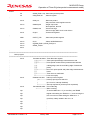
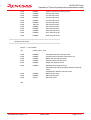
APPLICATION NOTE
M16C/62P Group
Operation of Timer B (pulse period measurement mode)
1.
Abstract
In pulse period/pulse width measurement mode, choose functions from those listed in Table 1. Operations of the
circled items are described below. Figure 1 shows the operation timing, and Figure 2 shows the set-up
procedure. A reference program is an example when using the Timer B0 interrupt based on the setting
procedure of Figure 2.
2.
Introduction
This application note is applied to the M16C/62P group Microcomputers.
This program can be operated under the condition of M16C family products with the same SFR(Special
Function Register) as M16C/62P Group products. Because some functions may be modified of the M16C family
products, see the user’s manual. When using the functions shown in this application note, evaluate them
carefully for an operation
REJ05B0545-0110/Rev.1.10
January 2006
Page 1 of 10
M16C/62P Group
Operation of Timer B (pulse period measurement mode)
3.
Choosed functions
Table 1. Choosed functions
Item
Set-up
Count source
O
Internal count source (f1 / f8 / f32 / fc32)
Measurement
mode
O
Pulse period measurement (interval between measurement pulse falling edge to falling edge)
Pulse period measurement (interval between measurement pulse rising edge to rising edge)
Pulse width measurement (interval between measurement pulse falling edge to rising edge,
and between rising edge to falling edge)
4.
Operation
(1) Setting the count start flag to “1” causes the counter to start counting the count source.
(2) If a measurement pulse changes from “H” to “L”, the value of the counter goes to “0000h”, and
measurement is started. In this instance, an indeterminate value is transferred to the reload register.
The timer Bi interrupt request does not generate.
(3) If a measurement pulse changes from “H” to “L” again, the value of the counter is transferred
to the reload register, and the timer Bi interrupt request bit goes to “1”. Then the value of the counter
becomes “0000h”, and the measurement is started again.
Note
● The timer Bi interrupt request bit goes to “1” when an effective edge of a measurement pulse is input or
timer Bi is overflowed. The factor of interrupt request can be determined by use of the timer Bi overflow flag
within the interrupt routine.
● The value of the counter at the beginning of a count is indeterminate. Therefore, the timer Bi overflow flag may
go to “1” and timer Bi interrupt request may be generated during the interval between a count start and an
effective edge input.
● The timer Bi overflow flag is indeterminate after reset. The timer Bi overflow flag goes to “0” if timer Bi mode
register is written to when the count start flag is “1”. This flag cannot be set to “1” by software.
Measurement of pulse time interval from falling edge to falling edge
(1) Start count
(2) Start measurement
(3) Start measurement again
Count source
Measurement pulse
“H”
“L”
Transfer
(indeterminate value)
Reload register Å counter
transfer timing
(Note 1)
Timing at which counter
reaches “000016”
(Note 1)
Transfer
(measured value)
(Note 2)
“1”
Count start flag
“0”
Cleared to “0” when interrupt request is accepted, or cleared by software
“1”
Timer Bi interrupt
request bit
“0”
Timer Bi overflow flag
“1”
“0”
Note 1: Counter is initialized at completion of measurement.
Note 2: Timer has overflowed.
Figure 1. Operation timing of pulse period measurement mode
REJ05B0545-0110/Rev.1.10
January 2006
Page 2 of 10
M16C/62P Group
Operation of Timer B (pulse period measurement mode)
Selecting pulse period / pulse width measurement mode and functions
b7
b0
0
0
1
Timer Bi mode register (i=0 to 5) [Address 039B16 to 039D16, 035B16 to 035D16]
TBiMR (i=0 to 5)
0
Selection of pulse period / pulse width measurement mode
Measurement mode select bit
b3 b2
0 0 : Pulse period measurement
(Interval between measurement pulse falling edge to falling edge)
Fixed to “0” in pulse period/pulse width measurement mode (i = 0, 3)
In an attempt to write to this bit, write “0” (i = 1, 2, 4, 5)
Timer Bi overflow flag
0 : Timer did not overflow
1 : Timer has overflowed
Count source select bit
b7 b6
b7 b6
Count source period
Count
source f(XIN) : 16MHZ f(XCIN) : 32.768kHZ
0
0
f1
62.5ns
0
1
f8
500ns
1
0
f32
1
1
fc32
0 0 : f1
0 1 : f8
1 0 : f32
1 1 : fc32
2us
976.56us
Setting clock prescaler reset flag
(This function is effective when fC32 is selected as the count source. Reset the prescaler for generating fC32 by
dividing the XCIN by 32.)
b7
b0
Clock prescaler reset flag [Address 038116]
CPSRF
Clock prescaler reset flag
0 : No effect
1 : Prescaler is reset (When read, the value is “0”)
Setting count start flag
b7
b0
b7
Count start flag
[Address 038016]
TABSR
Timer B0 count start flag
Timer B1 count start flag
Timer B2 count start flag
b0
Timer B3,4,5 count start
flag
[Address 034016]
TBSR
Timer B3 count start flag
Timer B4 count start flag
Timer B5 count start flag
Start count
Clearing overflow flag
b7
b0
0
Timer Bi mode register (i=0 to 5) [Address 039B16 to 039D16, 035B16 to 035D16]
TBiMR (i=0 to 5)
Timer Bi overflow flag
0 : Timer did not overflow
Figure 2. set-up procedure of pulse period measurement mode
REJ05B0545-0110/Rev.1.10
January 2006
Page 3 of 10
M16C/62P Group
Operation of Timer B (pulse period measurement mode)
5.
The example of reference program
;**************************************************************************************
;
; M16C/62P Program Collection
;
; FILE NAME : rjj05b0704_src.a30
; CPU
: M16C/62P Group
; FUNCTION : Operation of Timer B (pulse period measurement mode)
; HISTORY : 2004.12.24 Ver 1.00
;
: 2006.1.25 Ver 1.10
;
; Copyright(C)2006, Renesas Technology Corp.
; Copyright(C)2006, Renesas Solutions Corp.
; All rights reserved.
;
;**************************************************************************************
;**************************************************************************************
;
Include
;**************************************************************************************
;
.LIST
off
;Stops outputting lines to the assembler list file
.INCLUDE sfr62p.inc
;Reads the file that defined SFR
.LIST
on
;Starts outputting lines to the assembler list file
;
;**************************************************************************************
;
Symbol definition
;**************************************************************************************
;
RAM_TOP
.equ
00400h
;Start address of RAM
RAM_END
.equ
013ffh
;End address of RAM
ROM_TOP
.equ
0f4000h
;Start address of ROM
VECT_TOP
.equ
0ffe00h
;Start address of vect_top
FIXED_VECT_TOP
.equ
0fffdch
;Start address of fixed_vect_top
SB_BASE
.equ
00380h
;Base address of sb
;
;**************************************************************************************
;
Program area
;**************************************************************************************
;=============================================================================
;
Start up
;=============================================================================
;
.section program,code
;Declares section name and section type
.org
ROM_TOP
;Declares start address
.sb
SB_BASE
;
;
REJ05B0545-0110/Rev.1.10
January 2006
Page 4 of 10
M16C/62P Group
Operation of Timer B (pulse period measurement mode)
START:
ldc
ldc
#RAM_END+1,isp ;Sets interrupt stack pointer
#SB_BASE,sb
;Sets sb register
mov.b
#03h,prcr
mov.w
#0800h,pm0
mov.w
#2008h,cm0
mov.b
#0,prcr
;Removes protect
;Set processor mode registers 0 and 1
;Single-chip mode
;No expansion, No wait
;Xcin-Xcout High
;Xin-Xout High, Main clock is No divison
;Protects all registers
ldintb
#VECT_TOP
;Sets interrupt table register
mov.w
mov.w
mov.w
sstr.w
#0,r0
;Clears WORKRAM area
#((RAM_END+1)-RAM_TOP)/2,r3
#RAM_TOP,a1
;
;
;
;=============================================================================
;
Main program
;=============================================================================
mov.b
#01000010b,tb0mr ;Timer B0 mode register
;
| | | | | | ++-----------;Pulse period/pulsewidgh measurement mode
;
| | | | ++--------------;Pulse period measurement (measurement between
;
||||
;a falling adge ;and the next falling adge of measured
;
||||
;pulse)
;
| | | +-----------------;Set to“0”in pulse period and pulse widge measurement
;
|||
;mode
;
| | +-------------------;Timer has not overflowed
;
++--------------------;Count source(f8)
mov.b
#00000011b,tb0ic ;Interrupt control register
;
|+++------------;Interrupt priority level select bit
;
|
;(011:Level 3, interrupt disabled)
;
+-----------------;Interrupt request bit (0:interrupt not requested)
mov.b
#00100000b,tabsr ;Count start flag
;
+-------------------;Starts counting
nop
;To set the MR3 bit to “0” (no overflow), set TBiMR
nop
;register with setting the TBiS bit to “1” and counting the
nop
;next count source after setting the MR3 bit to “1”
nop
;(overflow). Newly added in the Ver 1.10
nop
;
nop
;
nop
;
nop
;
REJ05B0545-0110/Rev.1.10
January 2006
Page 5 of 10
M16C/62P Group
Operation of Timer B (pulse period measurement mode)
fset
mov.b
;
MAIN:
i
;Set interrupt enable flag
#01000010b,tb0mr ;Timer B0 mode register
+-------------------;Timer did not overflowed
jmp
MAIN
;=============================================================================
;
Interrupt program
;=============================================================================
TB0_INT:
;
;
;/ TB0 interrupt routine /
;
reit
;
;=============================================================================
;
Dummy interrupt processing program
;=============================================================================
DUMMY:
reit
;
;**************************************************************************************
;
Setting of variable vector table
;**************************************************************************************
;
.section vect,romdata
.org
VECT_TOP + (4 * 4)
;
.lword
DUMMY
;INT3 interrupt vector
.lword
DUMMY
;TB5 interrupt vector
.lword
DUMMY
;TB4 interrupt vector
;UART1 bus collision detection interrupt vector
.lword
DUMMY
;TB3 interrupt vector
;UART0 bus collision detection interrupt vector
.lword
DUMMY
;SI/04/INT5 interrupt vector
.lword
DUMMY
;SI/03/INT4 interrupt vector
.lword
DUMMY
;UART2 bus collision detection interrupt vector
.lword
DUMMY
;DMA0 interrupt vector
.lword
DUMMY
;DMA1 interrupt vector
.lword
DUMMY
;KEY interrupt vector
.lword
DUMMY
;A-D interrupt vector
.lword
DUMMY
;UART2 transmit/NACK interrupt vector
.lword
DUMMY
;UART2 receive/ACK interrupt vector
.lword
DUMMY
;UART0 transmit/NACK interrupt vector
.lword
DUMMY
;UART0 receive/ACK interrupt vector
.lword
DUMMY
;UART1 transmit/NACK interrupt vector
REJ05B0545-0110/Rev.1.10
January 2006
Page 6 of 10
M16C/62P Group
Operation of Timer B (pulse period measurement mode)
.lword
.lword
.lword
.lword
.lword
.lword
.lword
.lword
.lword
.lword
.lword
.lword
DUMMY
DUMMY
DUMMY
DUMMY
DUMMY
DUMMY
TB0_INT
DUMMY
DUMMY
DUMMY
DUMMY
DUMMY
;UART1 receive/ACK interrupt vector
;TA0 interrupt vector
;TA1 interrupt vector
;TA2 interrupt vector
;TA3 interrupt vector
;TA4 interrupt vector
;TB0 interrupt vector
;TB1 interrupt vector
;TB2 interrupt vector
;INT0 interrupt vector
;INT1 interrupt vector
;INT2 interrupt vector
;
;**************************************************************************************
;
Setting of fixed vector
;**************************************************************************************
;
.section f_vect,romdata
.org
FIXED_VECT_TOP
;
.lword
DUMMY
;Undefined instruction interrupt vector
.lword
DUMMY
;Overflow (INTO instruction) interrupt vector
.lword
DUMMY
;BRK instruction interrupt vector
.lword
DUMMY
;Address match interrupt vector
.lword
DUMMY
;Single-step interrupt vector
.lword
DUMMY
;Watchdog timer interrupt vector
;Oscillation stop and Re-oscillation detection interrupt
;vector
;Voltage down detection interrupt vector
.lword
DUMMY
;DBC interrupt vector
.lword
DUMMY
;NMI interrupt vector
.lword
START
;Sets start vector
;
.end
REJ05B0545-0110/Rev.1.10
January 2006
Page 7 of 10
M16C/62P Group
Operation of Timer B (pulse period measurement mode)
6.
Referense
Hardware manual
M16C/62P Group Hardware Manual
(Use the most recent version of the document on the Renesas Technology Web site.)
Technical news/Technical update
(Use the most recent version of the document on the Renesas Technology Web site.)
REJ05B0545-0110/Rev.1.10
January 2006
Page 8 of 10
M16C/62P Group
Operation of Timer B (pulse period measurement mode)
Web-site and contact for support
Renesas Technology Web site
http://www.renesas.com/en/m16c
Inquiries
http://www.renesas.com/inquiry
[email protected]
Revision
Revised
Rev.
Issue data
1.00
2004.12
-
First edition issued
1.10
2006.01
5
Reference program modified
REJ05B0545-0110/Rev.1.10
Page
Point
January 2006
Page 9 of 10
M16C/62P Group
Operation of Timer B (pulse period measurement mode)
安全設計に関するお願い
Keep safety first in your circuit designs!
1. Renesas Technology Corporation puts the maximum effort into making semiconductor products
better and more reliable, but there is always the possibility that trouble may occur with them. Trouble
with semiconductors may lead to personal injury, fire or property damage.
Remember to give due consideration to safety when making your circuit designs, with appropriate
measures such as (i) placement of substitutive, auxiliary circuits, (ii) use of nonflammable material or
(iii) prevention against any malfunction or mishap.
Notes regarding these materials
1. These materials are intended as a reference to assist our customers in the selection of the Renesas
Technology Corporation product best suited to the customer's application; they do not convey any
license under any intellectual property rights, or any other rights, belonging to Renesas Technology
Corporation or a third party.
2. Renesas Technology Corporation assumes no responsibility for any damage, or infringement of any
third-party's rights, originating in the use of any product data, diagrams, charts, programs,
algorithms, or circuit application examples contained in these materials.
3. All information contained in these materials, including product data, diagrams, charts, programs and
algorithms represents information on products at the time of publication of these materials, and are
subject to change by Renesas Technology Corporation without notice due to product improvements
or other reasons. It is therefore recommended that customers contact Renesas Technology
Corporation or an authorized Renesas Technology Corporation product distributor for the latest
product information before purchasing a product listed herein.
The information described here may contain technical inaccuracies or typographical errors.
Renesas Technology Corporation assumes no responsibility for any damage, liability, or other loss
rising from these inaccuracies or errors.
Please also pay attention to information published by Renesas Technology Corporation by various
means, including the Renesas Technology Corporation Semiconductor home page
(http://www.renesas.com).
4. When using any or all of the information contained in these materials, including product data,
diagrams, charts, programs, and algorithms, please be sure to evaluate all information as a total
system before making a final decision on the applicability of the information and products. Renesas
Technology Corporation assumes no responsibility for any damage, liability or other loss resulting
from the information contained herein.
5. Renesas Technology Corporation semiconductors are not designed or manufactured for use in a
device or system that is used under circumstances in which human life is potentially at stake.
Please contact Renesas Technology Corporation or an authorized Renesas Technology Corporation
product distributor when considering the use of a product contained herein for any specific
purposes, such as apparatus or systems for transportation, vehicular, medical, aerospace, nuclear,
or undersea repeater use.
6. The prior written approval of Renesas Technology Corporation is necessary to reprint or reproduce
in whole or in part these materials.
7. If these products or technologies are subject to the Japanese export control restrictions, they must
be exported under a license from the Japanese government and cannot be imported into a country
other than the approved destination.
Any diversion or reexport contrary to the export control laws and regulations of Japan and/or the
country of destination is prohibited.
8. Please contact Renesas Technology Corporation for further details on these materials or the
products contained therein.
本
資料ご利用に際しての留意事項
REJ05B0545-0110/Rev.1.10
January 2006
Page 10 of 10