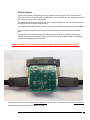
1
FuturePlus Systems Corporation
FS4439 DPv1.2 State Analysis
Probe
User Manual
For use with Keysight Logic Analyzers
Revision – 1.5
Copyright 2012 FuturePlus Systems Corporation
FuturePlus is a registered trademark of FuturePlus Systems Corporation
How to reach us ......................................................................................................................... 3
Product Warranty ...................................................................................................................... 4
Limitation of Warranty ..................................................................................................................... 4
Exclusive Remedies .........................................................................................................................................4
Assistance ............................................................................................................................................ 4
How to Use This Manual ................................................................................................................... 5
Introduction ............................................................................................................................... 5
Definitions ........................................................................................................................................... 5
Probe Function Overview.................................................................................................................. 6
FS4439 Input, Output, and Communication, in all modes ...............................................................................6
Aux Port Processing in all modes.....................................................................................................................6
Hi-speed Link Processing, similar functions in all modes................................................................................6
Functions unique to DP1.2 SST mode .............................................................................................................6
Functions unique to DP1.2 MST mode ............................................................................................................6
Analyzing the DP Bus ............................................................................................................... 7
Accessories Supplied .......................................................................................................................... 7
Minimum Equipment Required........................................................................................................ 7
Probing System Overview.......................................................................................................... 8
Front Panel ....................................................................................................................................... 10
FS4439 Probing Cables.................................................................................................................... 11
Installing your Software for the First Time .................................................................................. 15
Connecting the Keysight logic analyzer to the FS4439................................................................. 16
Logic Analyzer configuration files.................................................................................................. 17
Setting up the 1690x or Axie Analyzer ........................................................................................... 17
Offline Analysis ................................................................................................................................ 18
Probe Manager Application ............................................................................................................ 20
Mode Selection ..............................................................................................................................................22
DP 1.1a Mode ................................................................................................................................................22
DP 1.2 Mode SST & MST Probe Manager functions....................................................................................25
Probe Manager control of FS1041 Repeater ..................................................................................................28
Event Codes for SST and MST modes...........................................................................................................34
Triggering ......................................................................................................................................... 39
The Inverse Assembler .................................................................................................................... 41
General Information ............................................................................................................... 45
Characteristics.................................................................................................................................. 45
Standards Supported ......................................................................................................................................45
Power Requirements ......................................................................................................................................45
Logic Analyzer Required ...............................................................................................................................45
Environmental Temperature...........................................................................................................................45
Altitude ..........................................................................................................................................................45
Humidity ........................................................................................................................................................45
Testing and Troubleshooting..........................................................................................................................45
2
How to reach us
For Technical Support:
FuturePlus Systems Corporation
36 Olde English Road
Bedford NH 03110
TEL: 603-471-2734
FAX: 603-471-2738
On the web http://www.futureplus.com
For Sales and Marketing Support:
FuturePlus Systems Corporation
TEL: 603-472-5095
On the web http://www.futureplus.com
FuturePlus Systems has technical sales representatives in several major countries.
For an up to date listing please see http://www.futureplus.com/contact.html.
This product is covered in the EC under the WEEE Directive. Please go to
www.futureplus.com for recycling information
3
Product Warranty
This FuturePlus Systems product has a warranty against defects in material and workmanship for a
period of 1 year from the date of shipment. During the warranty period, FuturePlus Systems will, at its
option, either replace or repair products proven to be defective. For warranty service or repair, this
product must be returned to the factory.
Due to the complex nature of the FS4439 and the wide variety of customer target
implementations, the FS4439 has a 30 day acceptance period by the customer from the date of
receipt. If the customer does not contact FuturePlus Systems within 30 days of the receipt of the
product it will be said that the product has been accepted by the customer. If the customer is not
satisfied with the FS4439 they may return the FS4439 within 30 days for a refund.
For products returned to FuturePlus Systems for warranty service, the Buyer shall prepay shipping
charges to FuturePlus Systems and FuturePlus Systems shall pay shipping charges to return the
product to the Buyer. However, the Buyer shall pay all shipping charges, duties, and taxes for products
returned to FuturePlus Systems from another country.
FuturePlus Systems warrants that its software and hardware designated by FuturePlus Systems for
use with an instrument will execute its programming instructions when properly installed on that
instrument. FuturePlus Systems does not warrant that the operation of the hardware or software will be
uninterrupted or error-free.
Limitation of
Warranty
The foregoing warranty shall not apply to defects resulting from improper or inadequate maintenance
by the Buyer, Buyer-supplied software or interfacing, unauthorized modification or misuse, operation
outside of the environmental specifications for the product, or improper site preparation or
maintenance. NO OTHER WARRANTY IS EXPRESSED OR IMPLIED. FUTUREPLUS SYSTEMS
SPECIFICALLY DISCLAIMS THE IMPLIED WARRANTIES OF MERCHANTABILITY AND FITNESS
FOR A PARTICULAR PURPOSE.
Exclusive
Remedies
THE REMEDIES PROVIDED HEREIN ARE BUYER’S SOLE AND EXCLUSIVE REMEDIES.
FUTUREPLUS SYSTEMS SHALL NOT BE LIABLE FOR ANY DIRECT, INDIRECT, SPECIAL,
INCIDENTAL, OR CONSEQUENTIAL DAMAGES, WHETHER BASED ON CONTRACT, TORT, OR
ANY OTHER LEGAL THEORY.
Assistance
Product maintenance agreements and other customer assistance agreements are available for
FuturePlus Systems products. For assistance, contact Technical Support.
4
Introduction
How to Use
This Manual
Definitions
This manual is organized to help you quickly find the information you need.
•
Analyzing the DP Bus chapter introduces you to the FS4439 and lists the minimum equipment
required and accessories supplied for DP bus analysis.
•
The State Analysis chapter explains how to configure the FS4439 to perform state analysis on
your bus.
•
The General Information chapter provides information on the operating characteristics, and cable
header pinout for the FS4439 probe.
The following terms are used to describe aspects of the DP bus:
•
Lane- One differential signal (2 wires).
•
Link - One set of up to 4 DP lanes. The FS4439 handles 1 DP and 1 Aux link.
•
SST (Single Stream Traffic), MST (Multi-Stream Traffic)
5
Probe Function
Overview
The FS4439 probe is capable of connecting to DisplayPort links running in any of three modes
(v1.1a, v1.2 SST, v1.2 MST) at 3 link speeds (1.62, 2.7 and 5.4 Gbps).
FS4439 Input, Output, and Communication, in all modes
•
•
•
•
•
•
•
•
8b10b Decode & serial to parallel conversion of serial links: 1, 2, and 4-lane, to 5.4 Gbps.
Support of two probe cable types (interposer and flying lead).
No Reference Clock from Target required.
Serial link input polarity controllable for each lane (lane inversion).
8b10b Error Counting indicates signal quality in each lane and is displayed in the log file.
th
DDR State processing on 1/10 recovered link clock to logic analyzer.
4 Bi-color LED Display, shows status of each lane
Field upgradeable Flash Memory.
Aux Port Processing in all modes
•
•
Delivery of probed Aux data to Logic Analyzer Pod connectors with single SDR state clock.
Probing of Hot Plug Detect (HPD) and display status to Logic Analyzer
Hi-speed Link Processing, similar functions in all modes
•
•
•
•
•
•
•
•
•
Lane Deskew, with ability to tailor the individual DP1.1a, SST and MST deskew functions.
Training Detect status to Probe Manager and Logic Analyzer Pods (different patterns for
DP1.1a & 1.2 Modes).
Data Descrambling, which may be enabled/disabled.
Nibble swapping on all secondary packets (excluding unprocessed MST streams).
Event Decode (different code tables for 1.1a & 1.2 Modes; excluding unprocessed MST
streams).
Pixel Not Recognizer (1 recognizer in DP1.1a or SST Mode, 4 Recognizers in MST Mode)
Filter (1 Filter in 1.1a or SST Mode, 4 Filters in MST Mode; excluding unprocessed MST
streams)
Error Detection (DP1.1a Mode: 4 sources, 1 LAI bit; DP1.2 Mode: 6 sources, 3 LAI bits)
Restart Logic allows probe to operate and continue capture through target reboots.
Functions unique to DP1.2 SST mode
•
•
Additional Training Patterns
Additional Secondary Packets
Functions unique to DP1.2 MST mode
Control Symbol Descrambling
Time Slot Counter, 6 bits to Logic Analyzer Pod Connectors
Processes any set of 4 Virtual Channels, remaining VCs are flagged as “un-processed”
MST Mode VC Tagging: 4 Selected VCs, with 3-bit tag to Logic Analyzer
4 Probe-Stream Processors, to handle any 4 user-selected Streams (Virtual Channels)
o Event Decode
o SDP nibble swap
o Pixel not-recognizer
o Filter
• MTP Header processing and checking
MST Mode VC Payload Demux and VC Payload Re-mux functions
•
•
•
•
•
6
Analyzing the DP Bus
This chapter introduces you to the FuturePlus Systems FS4439 preprocessor and lists the minimum
equipment required for analysis.
The FS4439 is a DP State Analysis preprocessor. The preprocessor can connect to the target by either
a cabled interposer, or flying leads. The “sideband” signals, such as AUX and HPD connect to the
probe using separate cables. The preprocessor itself is controlled by the Probe Manager software,
which runs under Windows and communicates with the preprocessor via a USB cable.
The FS4439 “snoops” a link without significantly degrading its signal integrity. The high speed serial
signal is deserialized and processed for packet identification by the FS4439 before being sent to the
logic analyzer connections. Additionally, the preprocessor provides trigger and filtering functions. The
dis-assembler software running on the logic analyzer provides information regarding the transactions
within the captured traffic.
Accessories
Supplied
Minimum
Equipment
Required
The FS4439 product consists of the following accessories:
•
The FS4439 preprocessor, power supply and cable,
•
Protocol Disassemblers (FS1195 and AuxPort1_2 for DP), FS4439 Probe Manager application and
USB driver application on a CD for either Windows XP or 7.
•
A USB cable is provided for connecting the FS4439 preprocessor to the Windows machine that the
Probe Manager is loaded on.
•
1 DisplayPort cable (2m M-M) to be used between the DP source (or FS1041 interposer) and the
DP sink. We STRONGLY recommend the use of this cable as it has been carefully tested to insure
it will not disturb signal integrity at HBR2 data rates.
•
This User Manual and Quick Start sheet.
The minimum equipment required for analysis of a DP consists of the following equipment:
•
Keysight logic analysis frame with logic analysis modules.
•
A DPI target bus.
7
Probing System Overview
The architecture of the FS4439 preprocessor and the design of the DP link to be probed
should both be thoroughly understood before attempting to use the probe.
The following is a general outline of the steps to be taken when probing a new link. Read
the following pages for more specific information.
The FS4439 preprocessor requires the understanding and correct set-up of 4 different systems
before a trace should be taken. These systems are
1. Probe Manager software. The software has two installation (.exe) programs associated with it,
one to load the USB drivers needed to establish USB connections between the probe HW and
the Probe Manager program, and the other is to install the Display Port 1.2 Probe Manager
GUI program.
The USB driver should be installed first.
All installation programs are located on the CD that comes with the FS4439.
The USBXpress software is identified as USBXpressInstaller.exe and the Probe Manager
software is identified as DisplayPort12_probe_XXX.exe, where XXX indicates the PC’s OS.
The Probe Manager GUI program is supported on the Windows XP or Windows 7 OS and has
a separate installation program for each OS. The appropriate installation program must be
executed for the OS on which the program will be loaded onto.
Install SiLabs Driver
Run the USBXpressInstaller.exe program that is located on the CDROM disk to install the
USBXpress driver that provides the USB connection to the probe HW.
Install Probe Manager Software
On Windows 7 PCs
Run the DisplayPort12_probe_manager_7.exe program that is located on the CDROM to
install the DP 1.2 Probe Manager GUI software.
On Windows XP PCS
Run the DisplayPort12_probe_manager_xp.exe program that is located on the CDROM to
install the DP 1.2 Probe Manager GUI software.
NOTE: The Microsoft .NET Framework must be on the system for the Probe Manager
application to load properly.
2. FS4439 probe. This preprocessor requires its own DC power supply which is provided.
Additionally, this preprocessor is completely initialized, set-up and controlled by the Probe
Manager software that resides on a Windows based system (either stand alone PC or logic
analyzer). All communication to the FS4439 preprocessor is by means of the USB port on the
PC (or logic analyzer). Improper or incomplete installation of either the correct USB driver or
the Probe Manager software will prevent operation of the FS4439.
8
3. Keysight Logic Analyzer. The configuration files for the logic analyzer are on a CD (FS1195
and AuxPort1_2). Install these files, either for Windows XP or 7, as required and follow the
instructions for logic analyzer module (card) interconnections and logic analyzer connections to
the FS4439 probe.
4. Target platform. There are several requirements of the DP platform in order to assure that the
FS4439 can successfully probe the target’s DP link with minimal impact to the link and errors
seen at the probe. These requirements are discussed in the Probe Cables section. There are
two probing cables, FS1041 interposer or flying lead. There are link attributes such as lane
inversion, data scrambling, and lane reversal, which need to be defined in the Probe Manager
in order for the preprocessor to capture data properly.
It is strongly recommended that the user methodically proceed in the following manner when
setting up the probe. There is more detail on each step on page 17.
1. Load the USB driver Installation software into the system that the Probe Manager software will
run on.
2. Load the Probe Manager software (USBXpressInstaller.exe) and FS1195/AUX.exe files on the
PC and/or logic analyzer.
3. Configure (merge) the logic analyzer modules as required, and run the Keysight Logic
analyzer’s internal diagnostics. If the analyzer passes, then make the appropriate target probe
connections to the FS4439 probe and from the probe to the Keysight logic analyzer. Use the
Properties button on the probes shown in the Overview screen of the Keysight application for
guidance on connecting the cables.
4. Connect the appropriate probing cable(s) to the target system, power up the probe. Wait until
the “Green” ready light appears on the FS4439. This can take up to 20 seconds after power
has been applied to the probe.
5. Open up the Probe Manager application and select the appropriate settings for the probe cable
being used and the target link. Check that the expected Pad assignments for the probed link
show green. For the first capture turn off all the filters. It is recommended that the first capture
be run at HBR rate (2.7Gbps).
6. If the FS4439 preprocessor Lane LEDs are all Green and the first trace file captured on the
logic analyzer has no error messages then it is a good indication that all initial settings are
correct.
7. A link showing any orange on an LED, needs settings for link width, lane reverse or lane
inversion adjusted in the Probe Config window.
Depending on the DP target system’s data lane signal characteristics, such as jitter tolerance,
jitter spectrum and BER, the user may always see some level of orange LED activity and see the
corresponding error counts recorded on the analyzer and in the Probe Error Log.
9
Front Panel
The connections and features of the FS4439 preprocessor include:
•
DC input for provided external AC to DC power supply (please note that the use of any other
power supply voids the warranty on the FS4439) and USB connections to the Windows
PC/169xx analyzer where the Probe Manager software will be loaded.
•
Link Probe cable connection for 1 of the probing cables (interposer or FL)
•
Logic Analyzer 90 pin pod connections. P1 – P4 are connections for HS Link, and P5 – P8 are
for AUX link.
•
Cables for connection to AUX and HPD.
•
READY LED indicates that the FS4439 Probe firmware is loaded and the probe is ready to
capture DP traffic.
•
LED indication of Lane status.
Lane Status
LED color
Green
Dark
Orange
Red
Meaning
Lane OK
Lane not active, or Probe
stopped
Data Invalid (8b10b error)
RX Error (loss of sync or
PLL lock)
10
FS4439 Probing
Cables
Target DP Link requirements
The eye requirements are measured by eye height and eye width, forming a diamond shape. These
requirements are listed below and described pictorially. The shape of the eye as seen by the FS4439
must closely resemble the wave shape shown below. Specifically the eye opening must not show a
decrease in amplitude prior to reaching the center of the unit interval.
Figure 4-Example of eye specifications as seen at the footprint pad
Description
Specification for
2.7Gbps
Specification for
5.4Gbps
Min Eye height
1
at footprint pad
175mV Vdiff p-p
90mV Vdiff p-p
Min Eye Width at
probe point
.45 UI (Jitter
tolerance of
3
0.55UI)
.45 UI (Jitter
tolerance of
3
0.55UI)
Length Matching
RequirementsDifferential Pair
+/-5mil
Skew tolerated
between lanes of
a link
24 ns
2
+/-5mil
2
24 ns
11
In order for the FS4439 to achieve a low error rate for the acquired data on the DisplayPort Main Link,
the Jitter Spectrum for the target must be within the jitter tolerance shown below. Users not adhering
to this specification do so with the knowledge that errors may be seen on the FS4439 and
incorrect protocol decode could result.
12
FS1041 Repeater
The FS1041 Repeater is designed as a DP link endpoint and fanout buffer. The FS1041 Repeater
terminates the line on it’s board and then retransmits 2 copies of the DP link. One copy goes to the DP
Sink, and one copy goes the FS4439 probe.
The cable from the DP Source is connected to the receptacle labeled “IN” and a second cable goes to
the DP Sink from the receptacle labeled “OUT”.
The FS4439 probe cables for AUX and HPD connect to their labeled headers on the FS1041 Repeater.
There is a green LED on the FS1041 repeater board that indicates it has power from the FS4439
probe.
The repeater nature of this test probe may interfere with the DP Source’s ability to respond to the
Sink’s requests on some commands. There are a number of electrical attributes that are adjustable
from the Probe Manager (see that section).
ALWAYS POWER OFF THE FS4439 BOX BEFORE CONNECTING OR DISCONNECTING PROBES
Note the “IN” connector is for the cable from the DP Source, and the “OUT” connector is for the cable to the DP Sink.
Note the pin #1 positions for the AUX and HPD headers.
13
AUX and Hot Plug Detect (HPD) signals
The AUX and HPD signals for DP need to be connected to the FS4439 preprocessor separately from
the data link probing cables. There are uniquely identified and labeled cables for doing this. These
must be properly oriented for polarity.
The DP AUX channel requires a high speed differential connection using a Samtec .050 header where
pins 1 and 3 are AUXp and AUXn. The HPD signal has its own cable that also connects to a .050
header, pin 1 is the signal and pin 2 is the ground connection.
NOTE: These signals cannot see voltages higher than 4 VDC or there is a risk of damaging the
preprocessor.
The KOV for these cable headers is shown below. The mating 3 pin header is part number:
Through-hole: Samtec TMS-103-02-S-S, Surface mount: Samtec FTR-103-02-S-S .
DisplayPort Auxiliary Channel – MUST be plugged in correct orientation
Pin 1
Pin 2
Pin 3
DP_AUX_P
NC
DP_AUX_N
Pin 1
Pin 2
Pin 3
DP_HPD
GND
NC
DisplayPort Hot Plug Detect
14
The following outlines the software installation procedure when using the preprocessor for
the first time. Please do not attach the preprocessor to the analyzer or computer that will
be controlling the preprocessor until told to do so.
Installing your
Software for the First
Time
1. Place the software CD that came with the product into the logic analyzer or computer that you
will be installing the software on. In the case of a machine that does not have a CD drive, the
machine will either have to be put on a network and the files loaded remotely or the CD files
can be transferred from a USB drive.
2. Navigate to the installation CD using Windows explorer and install the following files in this
order.
a. Silabs USB driver installation software folder - USBXpressInstaller.exe
b. DisplayPort12_probe_manager_7.exe. (Win7 version vs XP version)
c.
FS1195 and AuxPort1_2.exe Protocol Dis-assembler (Win7 version vs XP version)
3. Once all the above files have been installed, connect the FS4439 to the analyzer/computer via
the USB port. Power on the FS4439 probe.
Once all the previous steps have completed all necessary software as well as USB drivers will be
installed. This procedure only needs to be done on initial install. You may now go to the desktop and
click on the “DisplayPort 1.2” icon to start the probe manager.
*If you are installing on a PC to only control the FS4439 then you can omit the installation of the
FS1195 and AUX.exe, but you must follow the rest of the steps.
For instructions on loading system files please refer to the section on loading system files later in this
manual.
15
Connecting the
Keysight logic analyzer
to the FS4439
The FuturePlus Systems FS4439 connectors are designed to connect directly to the 90
pin header cables on the appropriate Keysight logic analyzer cards as shown below:
DP 1.2 Main Link
X1, X2, X4
5.4 GB/s
540 MHz
DP 1.2 Aux
Channel
16753-756
(2) cards “Turbo”
Mode”
4 pods
16950
(2) cards “Turbo”
Mode”
16962A
U4154A
4 pods
4 pods
Probe Clock Max.
Frequency
Logic Analyzer
67 KHz
4 pods
4 pods
4 pods (Transitional
timing)
FS4439
Comment
1
2
3
4
P1
P2
P3
P4
Clock
1
P5
P6
P7
P8
Clock
High Speed
Card 1 Pod
AUX
Card 2 Pod
2
3
4
When probing a single direction of an x1, x2 or x4 link, the FS4439 drives 4 pods of signals to the logic
analyzer.
It is important that before you load a system file you initiate a self-test on all your modules
installed in your logic analyzer to insure all modules are working properly.
16
Logic Analyzer configuration files
High Speed – The logic analyzer configuration files are installed in the “FS4439” desktop folder when
FS1195.exe is run. The configuration files are organized by DP protocol, V1.1a, V1.2 SST, and V1.2
MST. Within each of these 3 categories the configuration files are further broken down by bit rate (2.7
vs 5.4) and by type of logic analyzer card being used.
AUX – There is just 1 Aux Port configuration file in it’s desktop folder, AX439_1.xml.
Setting up the 1690x or Axie Analyzer
The Logic Analyzer is a PC based application that requires a PC running Windows OS with the
Keysight logic analyzer software installed or a 169xx frame.
Before installing the protocol decoder for the FS4439 on a PC you must install the Keysight logic
analyzer software first. Once the Keysight logic analyzer software is installed, you can install the
FS4439 protocol decoder by placing the CD-ROM disk into the CD-ROM drive of the target computer
or Analyzer and executing the .exe setup program that is contained on the disk. The .exe setup file can
be executed from within the File Explorer PC Utility. You must navigate to the FS1195.exe file on the
CD-ROM disk and then double click the FS1195.exe file from within the File Explorer navigation panel.
The installation procedure does not need to be repeated. It only needs to be done the first time
the Analysis Probe is used.
When the software has been licensed you should be ready to load a configuration file. You can access
the configuration files by clicking on the folder that was placed on the desktop. When you click on the
folder it should open up to display all the configuration files to choose from. If you put your mouse
cursor on the name of the file a description will appear telling you what the setup consists of, once you
choose the configuration file that is appropriate for your configuration the 16900 operating system
should execute. The protocol decoder automatically loads when the configuration file is loaded. If the
decoder does not load, you may load it by selecting tools from the menu bar at the top of the screen
and select the decoder from the list.
17
Offline Analysis
Data that is saved on a logic analyzer data as an *.ala file, can be imported back into the Keysight
Logic Analysis environment for review. You can do offline analysis on a PC if you have the Keysight
Windows-based Logic Analyzer software installed on the PC, if you need this software please contact
Keysight.
Offline analysis allows a user to be able to analyze a trace offline at a PC so it frees up the analyzer for
another person to use the analyzer to capture data.
If you have already used the license that was included with your package on a logic analyzer and would
like to have the offline analysis feature on a PC you may get additional licenses at no charge, please
contact FuturePlus.
In order to view decoded data offline, after installing the Keysight Windows-based Logic Analyzer
software on a PC, you must install the FuturePlus software. Please follow the installation instructions
for “Setting up the logic analyzer”. Once the FuturePlus software has been installed and licensed
follow these steps to import the data and view it.
From the desktop, double click on the Keysight logic analyzer icon. When the application comes up
there will be a series of questions, answer the first question asking which startup option to use, select
Continue Offline. On the analyzer type question, select Cancel. When the application comes all the
way up you should have a blank screen with a menu bar and tool bar at the top.
For data from a 1680/90/900 analyzer, open the .ala file using the File, Open menu selections and
browse to the desired .ala file.
After clicking “next” you must browse for the fast binary data file you want to import. Once you have
located the file and clicked start import, the data should appear in the listing.
After the data has been imported you must load the protocol decoder before you will see any decoding.
To load the decoder select Tools from the menu bar, when the drop down menu appears select
Inverse Assembler, then choose the name of the decoder for your particular product. The figure below
is a general picture; please choose the appropriate decoder for the trace you are working with.
18
19
Probe Manager Application
The USBXpress drivers must be installed before the probe manager GUI program can be installed.
The drivers can be installed by running the USBXpressInstaller.exe program that is located on the CD
provided in the Documentation packet.
The USBXpress drivers installation software can be found as the USBXpressInstaller.exe file on the
CD provided in the Documentation package. Insert the CD into the computer that will be used to control
the FS4439 probe. This computer must have a USB connection. Using Windows File Manager, Run
the USBXpressInstaller.exe (by double clicking it) and following the subsequent directions that follow.
Similarly, the DisplayPort12_probe_manager_7.exe (if you are running Windows XP then select the
DisplayPort12_probe_manager_XP.exe file) can be installed by double-clicking the appropriate
program on the CD, which initiates the installation software on the computer and places an icon on the
desktop. Follow the directions that follow including agreeing to the license terms, once the software
installation is complete click on finish. To start the program manager simply double click its desktop
icon.
The Probe Manager application detects all FS4439 probes that are connected to the USB bus and
allows the user to select which preprocessor will be controlled by the current instance of the Probe
Manager application from the initial screen as seen below.
The user configures and controls the preprocessor from the main form, which is composed of a menu
bar, a tool bar and a status message bar. The menu bar provides options that allow the user to
configure and run the probe. The tool bar provides options to configure the preprocessor and the
status bar displays the probes current status and/or any errors that may have been encountered. Error
messages displayed in the status bar are also logged in the Log Form if logging is enabled.
The “mode selection” drop down box gives the user the choice of one of three modes to choose for the
probe to run in.
•
•
•
DP version 1.1a protocol at either 1.67 or 2.7Gbps link rate
DP version 1.2 Single Stream (SST) at either 1.67, 2.7 or 5.4 Gbps.
DP version 1.2 Multi Stream (MST) at either 1.67, 2.7 or 5.4 Gbps.
20
The menu bar contains the following options:
File
•
Load File – Displays an open file dialog in which the user may navigate to and open
the file contains a previous session’s saved probed settings.
•
Save As - Displays a save file dialog in which the user may specify where a
preprocessor settings system file may be saved.
•
Exit – Shut down the application.
•
Modify Title String – Allows the user to specify the title string that appears in all subdialog’s title bar. This is helpful when running multiple probes.
Edit
Run/Stop
•
Run Probe Mgr – Running the preprocessor with the current settings. This is an
alternative to clicking the tool bar Run button.
•
Stop Probe Mgr - Stop the probe. This is an alternative to clicking the tool bar Stop
button.
21
Help
•
The Probe Manager application provides different selections to the user based on the
“Mode” that the FS4439 Probe is set to run. The sections of the User manual that
describe the configuration and use of the probe Manager are organized by Mode.
Mode Selection
DP 1.1a Mode
About – DisplayS version numbers for the Probe Manager application and FPGA
configuration.
Operation of the FS4439 in this mode will match the VESA Protocol specs for v1.1a on links of x1, x2,
or x4 at either 1.62 or 2.7 Gbps. The Configuration selections are shown below:
Note: there is no Config required for Aux signals
The functions provided on this screen include:
•
Selection of the Probing Cable type and Lane Width
22
•
While the preprocessor is stopped, signal activity indicators are provided on each channel.
Signal presence is indicated by an up-down arrow symbol and a lack of signal presence is
indicated by a flat horizontal line symbol. When the probe is in Run mode signal activity is
indicated by green or red (no activity).
•
Selection of Lane Reversal on each link.
•
Link Lane Descramble On or Off
•
Hot Plug Cable (HPD) Connection – If Connected is selected, then Aux decode requires the
HPD signal for operation.
•
Selection of Link rate, either 1.62 or 2.7 Gbps.
•
Selection of Toggle mode. When activated, the preprocessor output signals to the logic
analyzer pods and the link status LEDs are toggled.
Mode 1.1a Filter - functions are provides the user with a comprehensive suite of predefined filter
functions to apply to the high speed Link. These filters are state based, which means that the event has
to occur on all active lanes for it to be filtered.
Filtering out unwanted traffic such as dummy data symbols can extend the storage capabilities of the
logic analyzer. Filtering out irrelevant bus traffic can help users focus on specific packets of interest.
To filter out any particular traffic type, click on the appropriate box so a √ appears and click apply. You
must restart the preprocessor by pressing the green run button so the new values will be written to the
preprocessor hardware.
When “Decode Pixel States” is selected in the Protocol Decoder Preferences, then you cannot
filter Control Symbols.
Non-Uniform Pixel Identifier – The purpose of this tool is that it is to be used when the pixel values are
all expected to be a single value, which the user sets in the form shown below. The FS4439 will
produce a Trigger if it sees any Pixel value that is NOT Equal to the set value.
23
Log File - Once started, logging continues even if the preprocessor is stopped and started, or if the log
window is closed and re-opened. The log file will not repeat an error that repeats itself constantly.
Once a preprocessor has been stopped, the log entries can be written to a file of the user’s choice by
clicking the Write Log File button.
24
DP 1.2 Mode SST & MST Probe Manager functions
There are several changes to the Probe Manager Screens when DPv1.2 mode is selected.
The Probe Configuration screen has the following changes.
Probe SERDES adjustments - are used to “tune out” Receive errors shown as Orange LEDs on the
front panel of the FS4439. These adjustments are for use at HBR2 only. The DFE setting may provide
the most effect. If the default settings do not work, we would recommend adjusting DFE up to about 0A
as a stating point.
•
Receive EQ – is set at 2 (hex), the range for the setting is from 0 – 7.
•
DFE is set at 07 (hex), the range of values 0 – 1F. This adjustable on a per lane basis to allow
for SI variation between lanes.
ASSR (Alternate Scrambler Seed Reset) – Enabling this function changes the LFSR reset value used
on an SR from FFFF to FFFE. This is a function that is optional in eDP.
VC (Virtual Channel) Payload Time slots – In MST mode only, the v1.2 spec allows for video display
information to be broken up into 64 Payload Time Slots that are assigned to the individual video
streams (VCs) that are being carried on the DP link. This dialog allows the user to assign each possible
Time Slot to any of the up to 4 video streams that the FS4439 probe will capture and decode.
The information relating the VCs to each Time slot can be determined from the AUX channel State
listing for registers at addresses # 001C0:2h and 002C0:FFh.
Tag Only Mode – This disables the VC Stream processors and applies VC Tags 1-4.
25
The Filter Function has the following changes for v1.2 SST mode based on additional secondary data
packet types and Training patterns that were added to the DP specification:
26
The Filter Function has the following changes for v1.2 MST, which extends the SST Filtering functions
to include a separate Filter function for each Stream defined in the Configuration form and adds the
ability to filter within each stream based on it’s VC Payload fill or Stream Symbol.
27
Probe Manager control of FS1041 Repeater
If the user selects the Cable Type of FS1041 – Repeater, there are additional electrical parameters of
the DP High Speed link going to BOTH the DP Sink and the FS4439 probe that can be adjusted.
In general the user wants to use these controls to insure that there are Green LED Lane status
indications on the FS4439 probe, and that the Target Sink display is operating properly. The default
settings should be OK for RBR and HBR Link speeds.
NOTE: For the DP Link to work with the FS1041 Repeater, it has to be connected to the FS4439 probe,
the FS4439 needs to be powered on, and the Probe Manager Software needs to be open.
De-emphasis and VOD are output signal controls are applied across all 4 DP lanes in the Link, and are
independent for the Sink and the Probe.
The default value for De-emphasis is 0 DB. Use of De-emphasis is not recommended at VOD <
1000mV.
VOD is output differential amplitude. A Target Sink VOD that is too low will cause the monitor to turn
off.
28
The Equalization and Idle Threshold controls operate on the input signals from the DP Source and they
allow for individual Lane control.
The EQ Controls have a drop down that allow each lane to be set-up with either no EQ (bypass) or a 9
or 14.6 db boost at 3Ghz.
The Idle Threshold control allows for 4 different Idle assertion/deassertion levels, with a fixed 40 mV
threshold between them.
29
State Analysis
This chapter explains how to use the FS4439 to perform state analysis. The configuration file sets up
the format specification menu of the logic analyzer for compatibility with the output of the FS4439.
In order to get both the DP and AUX analyzers into the same Logic analyzer workspace as represented
in the Overview screen below, first load the appropriate DP configuration file depending on your
analyzer card. Then manually select the appropriate AUX configuration file using the “load” command
for the additional card that will show in the workspace.
30
DisplayPort High Speed Groups
Besides de-serializing the data stream for the logic analyzer, the FS4439 generates a number of
identification and control bits that are used by the Inverse Assembler and logic analyzer. These are
also available to the user and are described below. AUX port is defined separately.
v1.1a mode Logic analyzer signals per pod
Field
Bits
Definition
Pod
Bits
Storage
Data Error
Train1.1
spare
Probe DP1.1a Mode
Pixel Not Recognizer
Event Code
1
1
1
1
1
1
8
1=store
1=error
1= DP1.1a training
A4
16
15
14
13
12
11
10:3
spare
spare
Data Present [3,2,1,0]
LOS [3,2,1,0]
Lane 0 Invalid
Lane 0 Command
Lane 0 Data [7:3]
Lane 0 Data [2:0]
Lane 1 Invalid
Lane 1 Command
Lane 1 Data [7:0]
Lane 2 Invalid
Lane 2 Command
Lane 2 Data [7:6]
Lane 2 Data [5:0]
Lane 3 Invalid
Lane 3 Command
Lane 3 Data [7:0]
3
2
4
4
1
1
5
3
1
1
8
1
1
2
6
1
1
8
0= Probe is in DP1.1a mode
1= Pixel is detected with wrong color
Describes packet type, signal event, or
error event
A3
1= lane data byte is present
1= lane loss of signal
1= 8b10b error
1= Control symbol 0 = Data symbol
8b decoded value
8b decoded value
1= 8b10b error
1= Control symbol 0 = Data symbol
8b decoded value
1= 8b10b error
1= Control symbol 0 = Data symbol
8b decoded value
8b decoded value
1= 8b10b error
1= Control symbol 0 = Data symbol
8b decoded value
A2
A1
2:0
16:15
14:11
10:7
6
5
4:0
16:14
13
12
11:4
3
2
1:0
15:10
9
8
7:0
Clock is on A1 bit 16
31
Event Code symbol definitions mode v1.1a
Event Code Symbol
Mismatch
F0 Pixel
F0 Stuff Data Sym (including
FS/FE)
BS
SR
Content Protection BS
BF
F1 Pixel
F1 Stuff Data Sym (including
FS/FE)
Missed SR Hor. Blank BE
Horizontal Blanking BE
Horizontal Blanking VBID
Horizontal Blanking MVID
V_err Hor. Blank MVID
Horizontal Blanking MAUD
A_err Hor. Blank MAUD
SR
Horizontal Blanking Dummy
Horizontal Blanking Audio
Stream
Horizontal Blanking Audio TS
Horizontal Blanking Reserved
Horizontal Blanking Extension
Horizontal Blanking Info
Frame
Vertical Blanking BE
BE
Missed SR Ver. Blank BE
Vertical Blanking VBID
Vertical Blanking MVID
V_err Vert. Blank MVID
MVID
Vertical Blanking MAUD
MAUD
A_err Ver. Blank MAUD
Vertical Blanking Dummy
Dummy
Vertical Blanking MSA
MSA
Vertical Blanking Audio
Stream
Audio Stream
Vertical Blanking Audio TS
Vertical Blanking Reserved
Reserved
Audio TS
Vertical Blanking Extension
Bit 8
Bit 7
Bit 6
Bit
5
Bit
4
Bit
3
0
0
0
Video
0
1
1
Field
x
0
0
x
0
0
x
0
1
x
1
0
0
0
0
0
0
0
1
1
1
1
1
1
x
x
x
x
1
1
0
1
1
1
0
0
1
0
0
1
0
1
0
0
0
0
0
0
0
0
0
0
Blanking
0
0
0
0
0
0
0
0
0
0
Horizontal
0
0
0
0
0
0
0
x
0
0
0
0
0
0
0
0
0
0
0
1
0
0
0
0
0
0
0
0
0
0
0
0
0
0
0
0
0
0
0
0
0
0
0
0
0
0
0
Blanking
0
0
0
0
0
0
0
0
0
0
0
0
0
0
0
0
0
0
0
0
0
0
0
0
0
0
0
Bit
2
Bit 1
Bit 0
Err bits
Err bits
x
x
x
x
0
0
1
0
0
1
0
1
0
1
0
x
x
x
x
x
x
0
0
0
0
0
0
0
0
0
0
0
0
0
0
0
0
0
1
1
1
1
0
0
0
1
1
1
0
0
0
1
0
1
1
0
1
1
0
0
1
0
0
1
0
0
0
1
0
1
0
0
0
x
0
0
0
x
0
x
0
0
0
1
1
1
1
0
0
0
1
0
1
1
0
1
0
1
0
0
0
0
0
0
0
0
0
Vertical
1
X
1
1
1
1
X
1
X
1
1
X
1
X
1
0
0
0
0
0
0
0
0
0
0
0
0
0
0
1
0
0
0
0
0
0
0
1
1
1
1
1
1
1
0
0
0
0
1
1
1
1
0
0
0
1
1
1
1
0
1
1
1
0
1
1
1
0
0
0
0
0
1
1
0
x
X
1
0
0
1
0
0
0
1
0
0
0
0
0
x
x
x
0
0
x
0
0
0
x
0
0
0
0
0
X
1
1
X
X
1
1
1
1
1
1
1
0
0
0
0
0
0
0
0
1
1
0
1
0
1
0
0
1
1
0
0
0
0
0
0
0
0
0
0
0
0
32
Extension
Vertical Blanking Info Frame
Info Frame
Training
0
0
0
1
0
0
0
x
X
1
X
X
1
1
1
X
0
1
1
X
1
0
0
X
1
0
0
X
0
0
0
X
0
0
0
X
v1.2 SST mode Logic analyzer signals per pod
Field
Bits
Definition
Pod
Bits
Storage
Error bits [2:0]
Probe Mode
VC Tag [2:0]
1
3
1
3
A4
16
15:13
12
11:9
Pixel Not Recognizer
Event Code
not applicable
LOS [3,2,1,0]
Lane 0 Invalid
Lane 0 Command
Lane 0 Data [7:3]
Lane 0 Data [2:0]
Lane 1 Invalid
Lane 1 Command
Lane 1 Data [7:0]
Lane 2 Invalid
Lane 2 Command
Lane 2 Data [7:6]
Lane 2 Data [5:0]
Lane 3 Invalid
Lane 3 Command
Lane 3 Data [7:0]
1
8
6
4
1
1
5
3
1
1
8
1
1
2
6
1
1
8
1= store
Error bits
1= Probe is in DP1.2 mode
Virtual Channel tag bits
000 = Probe is in SST Mode
1= Pixel is detected with wrong color
Describes current state or packet type
“not applicable” bits are driven low
1= lane loss of signal
1= 8b10b error
1= Control symbol 0 = Data symbol
8b decoded value
8b decoded value
1= 8b10b error
1= Control symbol 0 = Data symbol
8b decoded value
1= 8b10b error
1= Control symbol 0 = Data symbol
8b decoded value
8b decoded value
1= 8b10b error
1= Control symbol 0 = Data symbol
8b decoded value
A3
A2
A1
8
7:0
16:11
10:7
6
5
4:0
16:14
13
12
11:4
3
2
1:0
15:10
9
8
7:0
The Clock is on A1 bit 16
The SST Mode Logic Analyzer bit assignments duplicate the MST Mode bit assignments.
33
Event Codes for SST and MST modes
Main Link Event Code
Pixel
Stuff (including FS/FE) (not in MST)
Content Protection BS
Content Protection SR
BS
SR
BE
Training
VBID
MVID
MAUD
Dummy (does not exist in MST mode)
MSA
SDP 0x02 Audio Stream
SDP 0x01 Audio TS
SDP 0x05 Audio Copy Mgmt Pkt
SDP 0x06 ISRC Packet
SDP 0x07 VSC Packet
SDP 0x04 Extension Packet
SDP 0x80+ Info Frame
SDP 0x00, 03, 70-7F Reserved
Bit 7
Bit 6
Vid=1
Blnk=0
Field
or
Vert=1
Hor=0
F
F
VH
VH
VH
VH
VH
0*
VH
VH
VH
VH
VH
VH
VH
VH
VH
VH
VH
VH
VH
1
1
0
0
0
0
0
0*
0
0
0
0
0
0
0
0
0
0
0
0
0
Bit
5
Bit
4
Bit
3
Bit
2
Bit
1
Bit
0
0
0
1
1
0
0
0
0
0
0
0
0
0
1
1
1
1
0
1
0
1
0
1
0
1
0
0
1
0
0
0
1
1
1
0
0
0
1
1
1
1
0
1
0
1
0
1
1
0
0
1
1
0
1
1
0
0
1
0
0
1
0
0
0
0
0
0
0
0
1
T2
0
1
0
0
1
0
1
0
0
0
1
1
0
0
0
0
0
1
1
0
T1
0
0
0
0
0
0
0
1
1
1
0
0
1
0
0
0
0
0
1
1
T0
1
0
1
1
0
0
0
1
0
0
0
0
1
VC
Tag
=0
In
MST
=1
2
3
or
4, or
5
SST Mode Event Decode occurs when VC Tag = 0.
The SST Mode Event Decode table otherwise duplicates the MST Mode table.
The Training Type bits are encoded: T[1:0] = 0 indicates symbol error rate measurement pattern.
T[1:0] = 1 indicates TP1. T[1:0] = 2 indicates TP2. T[1:0] = 3 indicates TP3. T[2] is a spare.
34
Event Code symbol definitions mode SST
Event Code Symbol
Bit 7
Bit 6
Bit
4
0
0
0
0
1
1
1
0
0
1
1
0
0
0
0
1
0
0
0
0
0
0
0
0
1
1
1
1
1
0
0
0
0
0
Bit
3
1
1
1
1
0
0
0
1
1
0
0
1
1
1
1
0
0
0
0
0
1
1
1
1
0
0
1
1
1
0
0
0
0
1
Bit
2
0
0
0
0
1
0
0
0
0
0
0
0
0
0
0
1
x
x
X
X
0
0
1
1
0
0
0
1
1
0
0
1
1
0
Bit 1
Bit 0
0
1
X
x
X
0
1
0
1
0
1
0
1
0
1
0
0
0
0
0
0
1
0
1
0
1
0
1
1
0
1
0
1
0
Bit
5
0
0
0
0
0
0
0
1
1
1
1
0
0
0
0
0
0
0
0
0
0
0
0
0
0
0
0
0
0
1
1
1
1
1
F0 Pixel
F1 Pixel
BS
SR
BE
F0 Stuff Data Sym (FS/FE)
F1 Stuff Data Sym (FS/FE)
Hor. Content. Prot. BS
Vert. Content. Prot. BS
Hor. Content. Prot. SR
Ver. Content. Prot. SR
Horizontal BS
Vertical BS
Horizontal SR
Vertical SR
Horizontal BE
Unknown
Training TP1
Training TP2
Training TP3
Horizontal VBID
Vertical VBID
Horizontal MVID
Vertical MVID
Horizontal MAUD
Vertical MAUD
Horizontal Dummy
Vertical Dummy
Vertical MSA
Horizontal Audio Stream
Vertical Audio Stream
Horizontal Audio TS
Vertical Audio TS
Horizontal Audio Copy Mgmt
Pkt
Vertical Audio Copy Mgmt Pkt
Horizontal ISRC Packet
Vertical ISRC Packet
Horizontal VSC Packet
Vertical VSC Packet
Horizontal Ext. Packet
Vertical Ext. Packet
Horizontal Info. Frame
Vertical Info. Frame
Horizontal Reserved
Vertical Reserved
1
1
0
0
0
1
1
0
0
0
0
0
0
0
0
0
0
0
0
0
0
0
0
0
0
0
0
0
0
0
0
0
0
0
0
0
1
1
0
0
0
0
0
0
0
1
1
1
1
0
0
0
1
1
0
0
0
0
0
0
0
0
0
0
0
0
0
1
0
0
0
1
1
0
0
0
0
0
0
0
0
1
1
1
0
1
0
1
1
1
0
0
1
1
1
0
0
0
0
0
0
1
0
0
0
0
0
0
0
0
0
0
0
1
0
1
0
1
0
1
0
1
0
1
1
1
1
0
0
1
1
0
0
1
1
0
1
1
1
1
1
1
1
1
0
0
1
0
0
0
0
1
1
0
0
0
0
0
0
0
0
0
1
1
1
1
0
0
1
1
1
1
1
0
0
0
0
1
1
1
0
0
0
0
0
0
0
0
1
1
35
Event Code symbol definitions mode MST
Event Code Symbol
Bit 7
Bit 6
Bit
4
0
0
0
0
0
0
1
0
0
0
0
0
0
0
0
1
1
1
0
0
0
0
0
Bit
3
1
1
1
1
1
1
0
0
0
0
0
1
1
1
1
0
0
1
0
0
0
0
1
Bit
2
0
0
0
0
0
0
1
x
x
X
X
0
0
1
1
0
0
1
0
0
1
1
0
Bit 1
Bit 0
0
1
X
x
0
1
0
0
0
0
0
0
1
0
1
0
1
1
0
1
0
1
0
Bit
5
0
0
0
0
0
0
0
0
0
0
0
0
0
0
0
0
0
0
1
1
1
1
1
F0 Pixel
F1 Pixel
BS
SR
Horizontal SR
Vertical SR
Horizontal BE
Unknown
Training TP1
Training TP2
Training TP3
Horizontal VBID
Vertical VBID
Horizontal MVID
Vertical MVID
Horizontal MAUD
Vertical MAUD
Vertical MSA
Horizontal Audio Stream
Vertical Audio Stream
Horizontal Audio TS
Vertical Audio TS
Horizontal Audio Copy Mgmt
Pkt
Vertical Audio Copy Mgmt Pkt
Horizontal ISRC Packet
Vertical ISRC Packet
Horizontal VSC Packet
Vertical VSC Packet
Horizontal Ext. Packet
Vertical Ext. Packet
Horizontal Info. Frame
Vertical Info. Frame
Horizontal Reserved
Vertical Reserved
SF
VCPF/RG
MTP Header = 0
MTP Header not = SR, 0, or
ACT
MTP Header = ACT
Unprocessed VC
1
1
0
0
0
0
0
0
0
0
0
0
0
0
0
0
0
0
0
0
0
0
0
0
0
1
1
1
1
0
0
0
1
1
0
0
0
0
0
0
0
0
0
0
0
1
0
0
0
1
1
1
1
0
1
0
1
1
1
0
0
1
1
0
0
0
0
0
1
0
0
0
0
0
0
0
0
0
0
0
X
X
0
0
1
0
1
0
1
0
1
0
1
0
1
X
X
0
0
1
1
1
0
0
1
1
0
0
1
1
1
1
1
1
0
1
1
1
1
1
1
1
1
0
0
1
1
1
1
1
0
0
0
0
1
1
0
0
0
0
0
1
1
0
0
0
0
0
0
1
1
1
1
0
0
0
0
1
1
1
1
1
1
1
0
0
0
0
1
1
1
0
1
0
1
0
0
0
0
0
0
0
0
1
1
1
0
1
0
0
0
0
0
1
0
1
0
0
1
0
1
0
1
1
0
36
Error detection
Error Type
No Error
Mismatch
V_err (MVID Check)
A_err (MAUD check)
Missed SR
Any Invalid
Loss of Sync
DP1.1a Mode
Analyzer Interface
Data Error
0
1
1
1
1
NA
NA
SST Mode
Analyzer Interface
ErrorBit[2:0]
000
001
010
011
100
101
110
MST Mode
Analyzer Interface
ErrorBit[2:0]
000
001
010
011
100
101
110
Mismatch - This error occurs when there when the KChar or configuration fields of the active lanes
don't match. Checks are made on all KChars and the VBID, MVID and MAUD fields.
V_err (MVID Check) – This error is detected when the no_video bit is set in the VBID and the MVID
field is not 0.
A_err (MAUD check - This error is detected when the audio_mute bit is set in the VBID and the
MVAUD field is not 0.
Missed SR
In 1.1a or SST mode - There is a BE counter on each of the four lanes. If 512 BEs are
received without receiving an SR on any lane the Missed SR error is asserted.
th
In MST mode - SR Control Symbol inserted in MTP Header time slot every 1024 MTP
as a Link Frame boundary marker, resulting in SR insertion interval of 2^16 time slots. So every
th
1024 multi-stream transport packet header is replaced with an SR or every 65536 time slot. This SR
is for a link frame boundary marker.
37
Aux Group
Aux Port is a half-duplex, bi-directional channel between DisplayPort transmitter (source) and
DisplayPort receiver (sink). It consists of 1 differential pair transporting self-clocked data. The AUX CH
supports a bandwidth of 1Mbps. The DisplayPort Source Device is the master (also referred to as
AUX CH requester) that initiates an AUX CH transaction. DisplayPort Sink Device is the slave (also
referred to as the replier) is the device that responds to the transaction.
Aux channel has its own clock (67KHz) so that it can be clocked into separate modules in the LA on a
separate clock domain. It also has its own Inverse Assembler that has to be loaded separately.
Field
Command
ADDR[11:0]
ADDR[19:12]
Aux CLK
DATA[7:0]
SYNC
Bits
4
12
8
1
8
1
STOP
Spare
Spare
Request
Response
Timeout
HPD event
1
1
1
1
1
1
2
HPD Valid
Storage
Byte Count
1
1
5
Definition
Command Field
Address Field
Address Field
Data field
Sync Bit
First part of the transfer, CMD, ADDR and DATA are
all updated, if SYNC is 0 then only DATA is updated.
Stop, last byte of the transfer.
High when transaction is request
High when transaction is response
Response Timer timeout period 300us
Bit 1 Bit0
Meaning
0
0
0
1
1
1
Probe
B1
B1
B2
B1
B2
B3
Channel
3:0
15:4
7:0
16
15:8
0
B3
B3
B3
B3
B3
B3
B3
1
2
3
4
5
6
8:7
B3
B3
B4
9
15
10:6
Unplugged HPD=Low (level)
HPD pulsed low .25ms to 1.50ms
Interrupt event (event signaled on
rising edge of HPD)
Plugged In HPD=High (level)
Indicates a valid HPD event
Indicates Valid states
Number of valid bytes received inclusive of current
state
The Storage bit should be used as a qualifier for storing AUX data.
The rate at which Storage is pulsed depends on the packet type. AUX transfers begin with a four bit
CMD, a 20 bit address and 8 bits of data. Some packet types contain additional data which will be
presented 8 bits at a time. For the additional bytes the Storage bit will be pulsed as each byte is ready,
the Command and ADDR Fields will be unchanged.
38
Triggering
The configuration files provide some logic analyzer based trigger set-ups that utilize the pre defined
symbols described earlier. There are Triggers for both the DisplayPort analyzer and the AUX
channel analyzer.
•
Remember to always use conditional storage for either DisplayPort or AUX. This is because
the probe’s clock is free running and the Storage bit is used to qualify what is sent to the logic
analyzer modules.
•
The Event Code field makes it easy to trigger on particular packet types.
To capture specific traffic use the channel signals that can assist in identifying the activity that you want
to capture. For example, to capture training use the signal TRAIN, which goes high during training
activity. Turning off descrambling when looking at training will properly display the K characters.
39
Acquiring Data
First, insure that the FS4439 is attached to its external power supply and configured, which would be
indicated by a green Ready LED. Open up the Probe Manager software and insure the appropriate
selections are made and applied, finally make sure that the preprocessor is connected via the
appropriate cable(s) to the target system.
Once connected, with the link active, open up the Probe Config window and select cable type, lane
width, and reference clock options. Verify that lane activity indicators show activity at the correct lanes.
Run the probe and observe the LEDs.
Link Status
LED color
Green
Dark
Orange
Red
Meaning
Lane OK
Lane not active, or Probe
stopped
Data Invalid (8b10b error)
RX Error (loss of sync or
PLL lock)
If a lane’s LED is red then there may be a need to select different options for lane width, lane reverse
or lane inversion in the Probe Config window.
If a Lane’s LED is Orange that indicates some level of Data errors on the link. Check Log file for a
count of the errors. BER for a DP link is specified as 10E-9, which at HBR2 (5.4Gbps) allows more
than 5 errors every second. All transient events, such as a single bit error or a packet clocked into the
analyzer, are stretched to short visible pulses on the LEDs.
We have seen significant sensitivity on HBR2 links to Source settings and the cable used between the
Source and Sink.
We recommend the following steps if Lane LEDs are Orange:
1. Use the 2m DP – DP cable provided by FuturePlus with the FS4439.
2. Increase the HS lane signal swing from the DP source.
3. Adjust the Serdes settings in the Probe configuration form of the Probe Manager.
The FS4439 should show a green Signal LED of any Link being probed. Configure the analyzer trigger
menu to acquire data. Select RUN and, as soon as there is activity on the bus, the logic analyzer will
begin to acquire data. The analyzer will continue to acquire data and will display the data when the
analyzer memory is full; the trigger specification is TRUE or when you select STOP.
40
The Inverse
Assembler
Captured DP data is as shown in the following figure which displays the decoded protocol
using the Inverse Assembler.
The FS4439 Inverse Assemblers will perform the following functions:
♦
♦
Decode all DP or AUX protocol data
Color code the transaction type. The colors used by the software are as follows:
o Main Stream Attributes: Blue
o Secondary Data Packets: Orange
o All other states: Green
41
Preferences
The preference settings for the decoder must be set properly to decode the traffic correctly. When
decoding MST traffic you must be sure to select the correct probe stream. If the wrong probe stream
value is chosen the decoder will not output anything, the column for the decoder will be blank. When
chosen for SST the probe stream selection has not effect.
Note: Setting “Decode Pixel States” in the Protocol Decoder Preferences will result in longer
processing time for the State Listing.
42
An example of the AUX State Listing Protocol Decode is shown below. Reads and Writes are
highlighted in Green
43
The following shows the Logic Analyzer Overview screen for MST operation with 4 Virtual Streams
defined. 4 Stream is the maximum # of streams that can defined.
There are 5 State Listings defined:
1. MST Listing – This shows an integrated view of all streams on the HS links. Each state is
labeled by it’s Stream and has it’s own Event and Error codes. This view is not completely
time-correlated with the sequence of events on the probed link because of the processing
skews associated with the # of Time Slots defined for each stream.
2. Probe Stream Listings (1:4) – These listings display only the information associated with a
particular Virtual Stream. There are Filter and Inverse Assembly functions associated with this
State display.
44
General Information
This chapter provides additional reference information including the
characteristics and signal connections for the FS4439 probe.
Characteristics
The following operating characteristics are not specifications, but are typical
operating characteristics for the FS4439 probe.
If the product is used in a manner not specified by manufacturer,
then the protection provided by the equipment may become impaired.
Standards Supported
DisplayPort version 1.1a, v1.2
Power Requirements
100-240VAC, 2 amps.
Logic Analyzer Required
Keysight 1690x frame and 2 of either 40 or 90 pins modules.
Environmental
Temperature
Operating: 20 to 30 degrees C ( 68 – 86 degrees F)
Altitude
Operating: 4,6000m (15,000 ft)
Non operating: 15,3000m (50,000 ft)
Humidity
Up to 80% relative humidity. Avoid sudden, extreme temperature changes
which would cause condensation on the FS4439 module.
Testing and
Troubleshooting
There are no automatic performance tests or adjustments for the FS4439
module. If a failure is suspected in the FS4439 module contact the factory or
your FuturePlus Systems authorized distributor.
Servicing
The repair strategy for the FS4439 is module replacement. However, if parts of the FS4439 module
are damaged or lost contact the factory for a list of replacement parts.
45