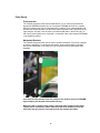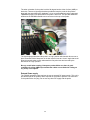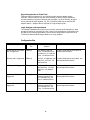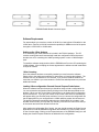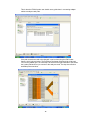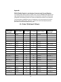
1
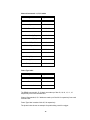
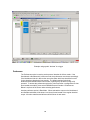
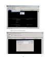
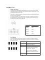
FuturePlus® Systems Corporation FBDIMM INTERPOSER PROBE FS2343 Users Manual For use with Agilent Technologies Logic Analyzers Revision 1.2 FuturePlus is a trademark of FuturePlus Systems Corporation Copyright 2004 FuturePlus Systems Corporation How to reach us.......................................................................................................................4 Product Warranty....................................................................................................................5 Limitation of warranty................................................................................................................... 5 Exclusive Remedies ....................................................................................................................................5 Assistance......................................................................................................................................... 5 Software License Agreement ..................................................................................................6 License Agreement.......................................................................................................................... 6 Use of the software.......................................................................................................................... 6 Copies and Adaptations.................................................................................................................. 6 Ownership ....................................................................................................................................... 6 Sublicensing and Distribution........................................................................................................ 6 Introduction.............................................................................................................................7 Probe Performance Limitation...................................................................................................... 7 Definitions........................................................................................................................................ 7 Logic Analyzer Modules ..............................................................................................................................7 Logic Analyzer Machine ..............................................................................................................................7 FS2343 Probe Description......................................................................................................8 Probe Technical Feature Summary .............................................................................................. 9 Probe Components.......................................................................................................................... 9 Probe Set-up ..........................................................................................................................10 Probe overview.............................................................................................................................. 10 Mechanical Brackets..................................................................................................................... 10 External Power supply ................................................................................................................. 11 Signal Assignments on Probe Pods.............................................................................................. 12 Logic Analyzer card requirements.............................................................................................. 12 Configuration files ................................................................................................................12 Software Requirements .........................................................................................................13 Setting up the 169xx Analyzer ..................................................................................................... 13 169xx Licensing ............................................................................................................................. 13 Loading 169xx configuration files and General Purpose Probe feature.................................. 13 Configuration File Labels ....................................................................................................15 Sampling labels ............................................................................................................................. 15 DRAM labels ................................................................................................................................. 15 Channel Command labels ............................................................................................................ 15 Default Trigger.............................................................................................................................. 16 2 Symbols..................................................................................................................................17 Preferences ............................................................................................................................19 SM (SMBus) Control ............................................................................................................21 Paddle card Settings ..................................................................................................................... 21 Probe Settings................................................................................................................................ 21 Event Bus Cabling ........................................................................................................................ 22 Probe Control Application ....................................................................................................22 Loading the Probe Control Software .......................................................................................... 22 Using the Probe Control Software .............................................................................................. 22 Setup...........................................................................................................................................................23 SB Commands ............................................................................................................................................24 Store Qualification......................................................................................................................................25 Trigger Events ............................................................................................................................................26 Event Bus ...................................................................................................................................................27 State Analysis Operation.......................................................................................................28 Setting Sample Positions .............................................................................................................. 28 State Display.................................................................................................................................. 30 Offline Analysis.....................................................................................................................30 Appendix................................................................................................................................33 FS2343 Paddle Signal to Logic Analyzer Connector and Channel Mapping.......................... 33 General Information .............................................................................................................45 Probe Connection .......................................................................................................................................45 Protocol supported......................................................................................................................................45 Logic Analyzer required.............................................................................................................................45 Logic Analyzer Adapter Cables required ...................................................................................................45 Service requirements ..................................................................................................................................45 3 How to reach us For Technical Support: FuturePlus Systems Corporation 36 Olde English Road Bedford NH 03110 TEL: 603-471-2734 FAX: 603-471-2738 On the web http://www.futureplus.com For Sales and Marketing Support: FuturePlus Systems Corporation TEL: 719-278-3540 FAX: 719-278-9586 On the web http://www.futureplus.com FuturePlus Systems has technical sales representatives in several major countries. For an up to date listing please see http://www.futureplus.com/contact.html. Agilent Technologies is also an authorized reseller of many FuturePlus products. Contact any Agilent Technologies sales office for details. 4 Product Warranty Due to wide variety of possible customer target implementations, the FS2343 FBDIMM Interposer probe has a 30 day acceptance period by the customer from the date of receipt. If the customer does not contact FuturePlus Systems within 30 days of the receipt of the product it will be determined that the customer has accepted the product. If the customer is not satisfied with the FS2343 FBDIMM Interposer probe they may return it within 30 days for a refund. This FuturePlus Systems® product has a warranty against defects in material and workmanship for a period of 1 year from the date of shipment. During the warranty period, FuturePlus Systems will, at its option, either replace or repair products proven to be defective. For warranty service or repair, this product must be returned to the factory. For products returned to FuturePlus Systems for warranty service, the Buyer shall prepay shipping charges to FuturePlus Systems and FuturePlus Systems shall pay shipping charges to return the product to the Buyer. However, the Buyer shall pay all shipping charges, duties, and taxes for products returned to FuturePlus Systems from another country. FuturePlus Systems warrants that its software and hardware designated by FuturePlus Systems for use with an instrument will execute its programming instructions when properly installed on that instrument. FuturePlus Systems does not warrant that the operation of the hardware or software will be uninterrupted or error-free. Limitation of warranty The foregoing warranty shall not apply to defects resulting from improper or inadequate maintenance by the Buyer, Buyer-supplied software or interfacing, unauthorized modification or misuse, or improper site preparation or maintenance. NO OTHER WARRANTY IS EXPRESSED OR IMPLIED. FUTUREPLUS SYSTEMS SPECIFICALLY DISCLAIMS THE IMPLIED WARRANTIES OF MERCHANTABILITY AND FITNESS FOR A PARTICULAR PURPOSE. Exclusive Remedies THE REMEDIES PROVIDED HEREIN ARE BUYER’S SOLE AND EXCLUSIVE REMEDIES. FUTUREPLUS SYSTEMS SHALL NOT BE LIABLE FOR ANY DIRECT, INDIRECT, SPECIAL, INCIDENTAL, OR CONSEQUENTIAL DAMAGES, WHETHER BASED ON CONTRACT, TORT, OR ANY OTHER LEGAL THEORY. Assistance Product maintenance agreements and other customer assistance agreements are available for FuturePlus Systems products. For assistance, contact the factory. 5 Software License Agreement IMPORTANT - Please read this license agreement carefully before opening the media envelope. Rights in the software are offered only on the condition that the customer agrees to all terms and conditions of the license agreement. Opening the media envelope indicates your acceptance of these terms and conditions. If you do not agree to the licensing agreement, you may return the unopened package for a full refund. License Agreement In return for payment for this product, FuturePlus Systems grants the Customer a SINGLE user LICENSE in the software subject to the following: Use of the software Customer may use the software on any one Agilent 1690x mainframe logic analysis system. • Customer may make copies or adaptations of the software. • Customer may not reverse assemble or decompile the software. Copies and Adaptations • Are allowed for archival purpose only. • When copying for adaptation is an essential step in the use of the software with the logic analyzer and/or logic analysis mainframe so long as the copies and adaptations are used in no other manner. Customer has no right to copy software unless it acquires an appropriate license to reproduce it from FuturePlus Systems. • Customer agrees that it does not have any title or ownership of the software, other than the physical media. Ownership • Customer acknowledges and agrees that the software is copyrighted and protected under the copyright laws. • Transfer of the right of ownership shall only be done with the consent of FuturePlus Systems. Sublicensing and Distribution Customer may not sublicense the software or distribute copies of the software to the public in physical media or by electronic means or any other means without the prior written consent of FuturePlus Systems. 6 Introduction Thank you for purchasing the FuturePlus Systems FS2343 FBDIMM Interposer Logic Analyzer Probe. We think you will find the FS2343, along with your Agilent Technologies Logic Analyzer, a valuable tool for helping to characterize and debug your FBDIMMbased systems. This Users Guide will provide the information you need to install, configure, and use the FBDIMM Interposer Probe. If you have any questions about this Guide or use of this probe, please contact FuturePlus Systems Corporation. Probe Performance Limitation The FS2343 Interposer probe is subject to the limitation inherent in probing the FBDIMM bus at 4 GHz and the extension of the high speed trace lengths of one FBDIMM slot by 65 mm. The probe is also dependent on the “logic analyzer interface” decode function of the Advanced Memory Buffer chip used as an interface between the FBDIMM High speed signals and the logic analyzer. If you have any questions please contact FuturePlus Systems. Definitions Logic Analyzer Modules "Module" - A set of logic analyzer cards that have been configured (via cables connecting the cards) to operate as a single logic analyzer whose total available channels is the sum of the channels on each card. A trigger within a module can be specified using all of the channels of that module. Each module may be further broken up into "Machines”. A single module may not extend beyond a single 5 card 16900 frame. Logic Analyzer Machine "Machine" - A set of logic analyzer pods from a logic analyzer module grouped together to operate as a single state or timing analyzer. 7 FS2343 Probe Description The FS2343 FBDIMM Interposer Probe is based on the “Logic Analyzer Interface (LAI) Mode” of the Advanced Memory Buffer chip used on Fully Buffered DIMMs. This mode allows decoding of the Primary Southbound (from memory controller to FBDIMMs) Commands and Data as well as Secondary Northbound Commands and Data from the interposed FBDIMM located in the card edge connector on the top of the FS2343 Interposer Probe. The probe can provide a single Southbound frame of 120 bits (10 lanes of 12 bits each) as well as a Northbound frame of 168 bits (14 lanes of 12 bits each) to the logic analyzer. On each line of the trace list a complete Northbound and Southbound frame is captured to simplify triggering. State Analysis of these frames is provided through the use of a Protocol Decoder. The probe requires control through a SMBus provided by the logic analyzer. This control is provided with the probe that runs on the 16900 workspace and is linked to the probe thru the SMBus ports in the logic analyzer cards when used with the 1690x series Agilent Logic Analyzer frames. 16753/4/5/6 as well as 16950 cards are supported. This LAI control Probe Add-In allows the user complete control over the LAI mode functions of the AMB used in the FS2343 to control Set-up, Triggering, Store Qualification, and AMB Register parameters. 8 Probe Technical Feature Summary • • • • Quick and easy connection between a 240 pin FBDIMM connector and Agilent 1690x Logic Analyzers. Complete and accurate state analysis of Primary South and Secondary Northbound FBDIMM traffic as seen by the AMB in LAI mode on the Interposer probe. Integrated control of Advanced Memory Buffer Logic Analyzer Interface functions. Ability to accept an FBDIMM and hence allow full backplane performance evaluation. Probe Components The following components have been shipped with your FS2343 Probe: • FS2343 Interposer Probe with cable attached Paddle card for logic analyzer connection • 1 10” EV cable, 3 .100” center pin jumpers, and mechanical brackets for support of the probe in either 180 degree or 90 degree orientations. • External AC power supply for the FS2343 Interposer probe. • CD containing Protocol Decode software for 1690x frame or offline analysis, as well as the Probe Control software • This Users Guide and other information on CD-ROM. • Quick Start Sheet. • Software Entitlement Certificate for 1690x or offline analysis. 9 Probe Set-up Probe overview The FS2343 Interposer probe uses an AMB device in “LAI” mode and provides the appropriate FBDIMM connections to an “interposed” FBDIMM device for it to operate within the memory bus. The LAI mode performs 2 functions. First, it demultiplexes and decodes the NB and SB traffic into the frame based information that is presented to the logic analyzer. Second, it acts as a link in the NB and SB chain in the memory bus. In this case it looks logically as an “upstream” or northside node to the interposed FBDIMM in its straddle connector. Mechanical Brackets The FS2343 Interposer probe can be used in several orientations. The first is a straight up from the backplane, or 180 degree orientation, which requires that the 2 straight brackets be assembled to the probe at its top and bottom with the associated nylon hardware. Care must be taken whenever the flex portion of the probe is moved, as FBDIMM signal integrity will degrade with repeated flexing. Make sure that no portion of the probe is touching other surfaces in the target system and be sure that the cables from the probe to the Paddle card are free from kinks and any sharp or hot surfaces that may damage the cables. 10 The other orientation for the probe is with a 90 degree bend to either it’s front (AMB) or back side. There are right angle brackets provided to keep the probe in this position along with the associated nylon hardware. It is our recommendation that the interposed FBDIMM be placed in the probe before the probe is bent over. This provides additional stiffness at the FBDIMM straddle mount connector on the top of the probe. The right angle brackets bend the probe in a “high” position which would allow a user to place a second FS2343 Interposer in the slot next to it bent at a “lower” angle that would allow the second probe to nest underneath the first probe bent and secured by the brackets in the “high” position. Be very careful when nesting 2 Interposer probes. Make sure there is good ventilation for all the AMB chips and that the cables are not kinked or resting on any sharp or hot objects. External Power supply The FS2343 Interposer probe requires the use an external DC power supply. This unit is provided as part of the product and is required for the probe to operate. It is connected to the probe with a mini plug. Do not use any other DC supply with the probe. 11 Signal Assignments on Probe Pods There are signal connections for up to 6 different logic analyzer adapter cables (E5378A). This provides the user with some flexibility in terms of which signals they connect to based on the type of analysis that is needed, e.g. SB or NB only, all trigger events, SB and NB traffic together, etc. The 16753/4/5/6 cards require the E5378A adapter cables. 1 Adapter cable is required for 2 logic analyzer pods. Logic Analyzer card requirements The FS2343 FBDIMM Probe requires up to five logic analyzer cards depending on what decode information is required by the user. There are several different configuration files provided for the following applications. Note: all these configurations require the use of 16753/4/5/6 cards and Dual Sample Mode in the Logic Analyzer. Configuration files Probe Configuration Configuration File Probe Connections to the Analyzer State Analysis requirement SB and NB up to 533 Mb/s with 10 trigger bits FB238_5 J10 (Master) Odd and Even, J13 Odd and Even, J9 odd/even, J11 Odd and Even, J12 Odd and Even 3 cards configured as one module for speeds up to 533 Mb/s SB Only and 8 Trigger bits FB238_4 J9 Even, J10 (Master) Odd and Even, J12 Even, J13 Odd and Even 3 cards configured as one module, one dual sample state machine NB Only and 9 Trigger bits FB238_3 J9 Odd and Even, J11 Odd and Even, J12 Odd and Even, J15 (Master) Odd 4 cards configured as one module, one dual sample state machine Full NB and SB with 5 Trigger bits FB238_2 J9 Odd and Even, J10 (Master) Odd and Even, J11 Odd and Even, J12 Odd, J13 Odd and Even 5 cards configured as one module, one dual sample state machine 12 lane NB and SB with 10 Trigger bits FB238_1 J9 Odd and Even, J10 (Master) Odd and Even, J11 Odd and Even, J12 Even, J13 Odd and Even 5 cards configured as one module, one dual sample state machine 12 FBDIMM Paddle Board Connector layout Software Requirements For state analysis you must have version A.02.99.00 or later Agilent OS installed on the 1690x frame. Version A.02.99.00 contains the capability for SMBus control of the probe through the 16753/4/5/6 or 16950 cards. Setting up the 169xx Analyzer A CD containing the 16900 software is included in the FS2343 package. The CD contains a setup file that will automatically install the configuration files and protocol decoder onto a PC containing the 16900 operating system or onto a 16900 analyzer itself. To install the software simply double click the FBDIMM.exe file on the CD containing the 16900 software. After accepting the license agreement the software should install within a couple of minutes. 169xx Licensing Once the software has been successfully installed you must license the software. Please refer to the entitlement certificate for instructions on licensing the software. The software can only be installed on one machine. If you need to install the software on more than one machine you must contact the FuturePlus sales department to purchase additional licenses. Loading 169xx configuration files and General Purpose Probe feature When the software has been licensed you should be ready to load a configuration file. You can access the configuration files by clicking on the folder that was placed on the desktop. When you click on the folder it should open up to display all the configuration files to choose from. If you put your mouse cursor on the name of the file a description will appear telling you what the setup consists of, once you choose the configuration file that is appropriate for your configuration the 16900 operating system should execute it. The protocol decoder automatically loads when the configuration file is loaded. If the decoder does not load, you may load it by selecting Tools from the menu bar at the top of the screen and select the decoder from the list. After loading the configuration file of choice, the user should see both the Probe Control application icon and the FBDIMM configuration and decoder icon in the Probes column on the Overview page. Clicking on the Properties button of the FBDIMM Config icon will display the General Purpose Probe Set as defined for this configuration. 13 This is what the FS2343 probe user should use to guide them in connecting adapter cables to analyzer card pods. If the pod connections need to be changed, it can be done using the Edit Probes feature, which is shown below. The Reference Designator field should be J9 through J15 from the paddle card. The next step is to select on the right hand side of the screen the 2 pods (Odd and Even) to connect to the analyzer cards. The drop box will show available pod connections. 14 Configuration File Labels The configuration files provided with the probe software have a number of labels defined that are useful in providing rapid identification of sampling position, DRAM, and Channel Command activity in the state listing. They can also be used as triggers for the logic analyzer. These labels include: Sampling labels There are 4 groups of Sampling labels which organize each bit sent for the probe to the logic analyzer by the location of its valid data window and therefore the required sampling position. This makes it more convenient to check the sampling set-up on a bit by bit basis. DRAM labels BA_x - Bank Address for Command Slot A, B or C as defined in 3 bits. _x is used to describe the Command slot. ADD_x - 16 bit label describing the DRAM address bus DS_x - 4 bits that direct the command to one of the eight possible DRAM DIMMs on the FBD channel. This is how any of the three commands in a frame can be directed to any DIMM in the FBD channel. These bits are used in some Channel Commands as well. RS_x - Rank Select bit. Channel Command labels SB_CMDA_CRC – Southbound Command Slot A CRC 14 bit value. FO_SB_CMDA_CRC – Failover Southbound Command Slot A CRC 10 bit value EV_x - Event Debug bits, 8 bits, used in the Channel Command Debug: In band events. PV_x – 8 bit Parameter Value that is associated with a debug event. This is used in the Channel Command Debug: In band events. DE_x - 8 bits, each bit refers to the CKE on each DIMM, DE0 would be for DIMM 0, DE1 would be for DIMM1, etc. RT_x - Relative timing, 10 timing bits communicate relative time of transfer across boundaries. Used in Channel Command Debug: Relative timing. PH_x - Phase bit, 6 bit field communicates the encoded boundary transfer phase. Used in Channel Command Debug: Relative timing. EX_x - 17 bit field that communicates debug information, used with Channel Command Debug: Exposed information. BCST_x - single bit field used in all CKE control commands (commands such as DRAM CKE per DIMM and DRAM CKE per Rank commands). A 1 value targets all DIMMs, if the bit is 0 the command targets only one DIMM specified by the DS bits. 15 TID – single Transaction identifier bit, used in Write Config. Register Channel Command. SD - Status delay, 2 bit field used in Sync command. Allows return status data to be delayed by up to 3 frames. EL0s - The EL0s bit indicates the channel should transition from the L0 state to the L0s state for exactly 42 frames. The L0 state is the state when the channel is ready to accept Channel and DRAM commands. The L0s state is an optional state used in systems that use power management. ERC - The ERC bit indicates that the channel should transition from L0 state to recalibrate state for exactly 42 frames. Used in Sync frame. IER – This bit indicates that commands and CRC errors be ignored by the AMB until after the next reset. Used in Sync frame. A10:2 - Address bus for Read or Write configuration Channel Commands. Default Trigger When a configuration file is loaded the default trigger will be set to trigger the analyzer when the Mode bit is = 0 and Frame = 1. When mode and frame are set at these values the AMB will be done with training sequences and the data that is on the channel is properly aligned and can be decoded properly by the decoder. 16 Symbols Terms used in the FBDIMM protocol are defined under labels that are referred to as symbols. Symbols can be used in defining triggers or for use in default store qualifications. Below is a list of labels with the symbols defined. When using a label for which symbols are defined, change the hex property to sym to display the symbol representation. A, B and C below refer to the command slot A, B, C respectively in the southbound frame. DRAM commands - A, B, C labels Symbol Symbol Value reserved 00 100x Enter Power down 00 1010 Exit Self Refresh 00 1011 Enter Self Refresh 00 1100 Auto Refresh 00 1101 Precharge Single 00 1110 Precharge All 00 1111 READ 01 0xxx WRITE 01 1xxx ACTIVATE 1x xxxx 17 Channel Commands - A, B, C labels Symbol Symbol Value Channel NOP 0000 000x Sync 00000 001x Soft Channel Reset 0000 010x reserved 0000 011x Read Config Reg 0000 100x Write Config Reg 0000 101x DRAM CKE per Rank 0000 110x DRAM CKE per DIMM 0000 111x reserved2 0001 0xxx reserved3 0001 10xx Debug Exposed 0001 110x Debug Relative 0001 1110 Debug In-Band 0001 1111 Frame Type label Symbol Symbol Value command 00 Reserved 01 Command + Wdata 1x The DRAM commands A, B, C labels are made up of bits 20, 19, 18, 12, 11, 10 respectively from each command slot. Channel Commands A, B, C labels are made up of bits 20-13 respectively from each command slot. Frame Type label consists of bits 25, 24 respectively. The picture below shows an example of symbols being used for a trigger. 18 Example using symbol “Activate” in a trigger Preferences The Preferences option is used to set the protocol decoder for failover mode. If the Southbound or Northbound is in failover mode, the preferences must be set accordingly. If the Northbound side is in failover the user must select which lane has failed in order for the decoder to decode the bus properly. The default settings for both the Northbound and Southbound are set to None, meaning they are both running at full potential. To access the preferences select the Tools menu after a configuration file has been loaded successfully, then select FBDIMM Protocol Decoder -1/Preferences. Below is a picture of the screen when selecting preferences. Another preference option is Raw Mode. When selected the output on the Northbound and Southbound labels will be shown in a binary format instead of the regular decoded output. All twelve transfers and all lanes will be shown in each state. 19 Below is a picture of the preference options 20 SM (SMBus) Control Paddle card Settings The FS2343 probe is designed so that AMB/LAI device control can be either from the 16900 logic analyzer and the Probe Control application software resident there, or from another FS2343 probe (slave mode). This feature is controlled by means of a 6 position switch on the probe paddle card near the logic analyzer connections. The factory configuration is for 16900 control of the probe. The settings on the switch are dependent on the configuration file used. The following picture shows the jumper and switch configurations on the paddle card. Config file SW# ON, all others off FB238_1 1 and 4 FB238_2 1 and 4 FB238_3 3 and 6 FB238_4 1 and 4 Probe Settings There is a 4 position jumper location at U8 on the top side of the FS2343 Interposer probe. There are jumpers that can be placed over each of the 4 set of pins. They have the following function: Jumper 5 1 8 Function 1-5 Probe ID bit 0 Address 20 2-6 Probe ID bit 1 Address 21 3-7 Jumper removed = AMB SMBus connected to analyzer at powerup. Factory config – installed 4 Jumper installed = AMB SMBus connected to motherboard at power up. 4-8 Unused 21 Event Bus Cabling The Event Bus bits, Evbus[0:3], from other probes can be daisy chained across multiple probes in order to provide cross probe control of other probes. There are 2 EV cable connectors on each probe and both connectors are wired in parallel so that either can be used. Additionally, the probe has termination sensing circuitry so that the Evbus[0:3] signals are properly terminated on the probe if the cables are not used. The cables are connected at either J9 or J10 on the board with their wires exiting the board from the top. LED D1 will light if the cables are attached backwards. Probe Control Application The FS2343 Interposer probe is controlled from a Probe Add-in, which has to be installed on the 16900 workspace as it communicates through the logic analyzer cards through an internal SM (SMBus) port which is connected to the probe by means of the adapter cable connection. Loading the Probe Control Software Load the CD provided with the probe into the 16900 frame and locate the file FBD Probe Control.exe. Double-click this file and it will install and be available in the Agilent Logic analyzer software under the Setup tab as the FBDIMM Probe. Using the Probe Control Software Always use the “Apply” button before changing windows or using the “OK” button. It is important to note that the probe control software sets up registers within the AMB. It is still necessary to set up parameters in the configuration file for triggers, storing, filtering etc. Setting up the AMB through the probe control software generates signals going to the logic analyzer, the logic analyzer can then use these signals to qualify, trigger or filter events or data of interest. Please see the following pages for details for the different register settings within the AMB. 22 Setup The Set-up screen provides control over basic probe use. • The probe Configuration setup button allows the user to select when they want to set up the parameters within the AMB. The choices are always after link training, before link training only when needed, or always before link training. If all you are interested in is data after link training then leave always after link training selected. • The probe can operate in a mode where lane data is only provided after L0s where the lane data is aligned to the clock, or in “raw” mode. Raw mode just passes data through to the logic analyzer, the lane data may not be aligned to the clocks at this point. • The “Restore” button resets ALL Probe settings to their factory configuration. • “Find Probe” pings the probe/AMB chip. 23 SB Commands This allows Match or Mask control over any 3 Command patterns entered by the user in either hex or binary format. Furthermore, each of 3 patterns can be searched for in either Command Slot A, B or C, or all three patterns in all 3 Command Slots. The mask and match feature allows the user to set 3 different command patterns along with data to mask out. The user can then specify 3 events, which allows a user to specify a frame containing 3 command values to be passed to the logic analyzer. When the frame occurs that satisfy the events specified, the data will be passed to the analyzer. 24 Store Qualification This section controls the operation of the Qual Flag, Qual Stop Delay, and Qual Period Delay. It allows the user to select from 32 different events for the definition of Qual Start and Qual Stop. These settings control the state of the Store_qual flag for non-filtered frames. The Store_qual flag in the configuration file can then be used for trigger events, default storing, etc. The Store_qual flag is controlled by this screen, the user may specify when to activate the Store_qual flag, specify an event to assert the Store_qual flag, and when to deassert the flag. 25 Trigger Events This capability allows the Probe user to define each of the AMB’s logic analyzer Triggers [0:10] to be set to one of 32 different event conditions seen by the AMB. It is important to note that not all LAITrig[0:10] signals are available to the logic analyzer. This is dependent on the configuration file loaded and the pod connections made to the logic analyzer. Each trigger bit has a corresponding label in the configuration file that can be used when specifying a trigger for the logic analyzer. 26 Event Bus This feature controls the operation of the Event Bus signals EV[0:3] which can be used for communication and triggering between probes in an FBDIMM Channel. 27 State Analysis Operation For proper state analysis the user must choose the correct configuration file to load depending on what type of analysis is desired, such as analyzing both Northbound and Southbound activity or just one direction. The list of configuration files provided is on page 12. Load the appropriate configuration file and use the General Purpose probe feature for proper cable attachment to the probe, for more information on the General Purpose probe feature please see the section titled “Loading 169xx configuration files and General Purpose Probe feature”. When the configuration file loads the decoder will automatically load providing the software has been properly licensed. For proper protocol decoder performance you must insure the preferences are set properly. Once the configuration file is loaded go to Tools, select FBDIMM Protocol Decoder -1 and select Preferences. Set the failover modes for the Southbound and or Northbound if necessary. The default settings are set to none. When you choose a Northbound failover mode you must select which lane(s) has failed as well. Once the configuration file has been loaded and all cables are attached to the probe, the next step is to configure the probe. Please refer to the section of the manual titled “Using the Probe Control Application”. The probe control application allows the user to set different parameters of the probe to allow certain data to be passed through to the analyzer. Setting Sample Positions In order to insure that the logic analyzer properly measures the output of the probe, the sample positions for each label need to be set properly. There are 4 “Sample Data” labels defined in each configuration file that group each North and Southbound data signal by its required sample position. It is recommended that Eyefinder is run on the logic analyzer while the target system is generating consistent traffic on the North and Southbound lanes. The sample positions in the config fields have been preset based on measurements in a test bed at 533MT/s data rates. They may need to be adjusted based on your target system. The following image shows the 4 “Sample Data” labels after an Eyefinder has been run. If there are clear eyes for each label, the user can drag all the blue sample position bars to the far left to aggregate them and then drag the single bar back to the window where it was originally located. If the sample positions are not set correctly then the data shown on the analyzer will not be correct. 28 After the probe has been configured, the trigger for the analyzer must be set. To set the trigger for the analyzer go to the setup menu bar and select “Advanced Trigger”. On the next window that pops up specify what you want the analyzer to trigger on. After you set the trigger, depress the run button (green arrow at the top of the screen on the overview, listing or waveform windows), the analyzer should be waiting for a trigger to occur at this point. Start a test on the target to generate traffic, when the trigger condition is satisfied the analyzer will continue capturing data until the memory is full or the user has depressed the stop button. When the analyzer has stopped the protocol decoder will automatically decode the data on the bus, the decoded data will appear under the Northbound and Southbound labels on the listing screen. 29 State Display Offline Analysis Offline analysis allows a user to be able to analyze a trace offline at a PC so it frees up the analyzer for another person to use the analyzer to capture data. If you have already used the FBDIMM Protocol Decoder license that was included with your package on a 1680/90/900 analyzer and would like to have the offline analysis feature on a PC you may buy additional licenses, please contact FuturePlus Sales department. In order to view decoded data offline, after installing the 1680/90/900 operating system on a PC, you must install the FuturePlus software. Please follow the installation instructions for “Setting up the 16900 analyzer”. Once the FuturePlus software has been installed and licensed follow these steps to import the data and view it. From the desktop, double click on the Agilent logic analyzer icon. When the application comes up there will be a series of questions, answer the first question asking which startup option to use, select Continue Offline. On the analyzer type question, select cancel. When the application comes all the way up you should have a blank screen with a menu bar and tool bar at the top. 30 For data from a 16900 analyzer, open the .ala file using the File, Open menu selections and browse to the desired .ala file. After clicking “next” you must browse for the fast binary data file you want to import. Once you have located the file and clicked start import, the data should appear in the listing. After the data has been imported you must load the protocol decoder before you will see any decoding. To load the decoder select Tools from the menu bar, when the drop down menu appears select Inverse Assembler, then choose the name of the decoder for your particular product. The figure below is a general picture; please choose the appropriate decoder for the trace you are working with. 31 After the decoder has loaded, select Preferences from the overview screen and set the preferences to their correct value in order to decode the trace properly. 32 Appendix FS2343 Paddle Signal to Logic Analyzer Connector and Channel Mapping The following table shows how the FS2343 Probe connects FBDIMM AMB signals to the logic analyzer pods and channels through the 100 pin Samtec connectors. Note that the configuration files described earlier use various combinations of these Pod connections. The nomenclature is NB/SB for North or Southbound, Lx for Lane number, Bx for bit in during the rising edge of Anly_clkp, and _xx is the bit for the Dual sampled (second) point which is on the falling edge of Anly_clkp. J9 - Pods 1(Odd) and 2 (Even) Signal name/Logical Signal Name NB_L1_B0_6 NB_L1_B4_10 NB_L0_B5_11 NB_L0_B3_9 NB_L1_B1_7 NB_L1_B5_11 NB_L0_B2_8 NB_L0_B1_7 NB_L2_B4_10 Logic Analyzer channel number SAMTEC Pin number SAMTEC Pin number Ground 1 2 Ground NC 3 4 NC Ground 5 6 Ground Odd D0 7 8 Even D0 Ground 9 10 Ground Odd D1 11 12 Even D1 Ground 13 14 Ground Odd D2 15 16 Even D2 Ground 17 18 Ground Odd D3 19 20 Even D3 Ground 21 22 Ground Odd D4 23 24 Even D4 Ground 25 26 Ground Odd D5 27 28 Even D5 Ground 29 30 Ground Odd D6 31 32 Even D6 Ground 33 34 Ground Odd D7 35 36 Even D7 Ground 37 38 Ground Odd D8 39 40 Even D8 Ground 41 42 Ground 33 Logic Analyzer channel number Signal Name/Logical Signal name MODE NB_L1_B2_8 FRAME NB_L0_B4_10 NB_L2_B1_7 NB_L2_B0_6 NB_L1_B3_9 NB_L3_B2_8 NB_L3_B0_6 Signal name/Logical Signal Name NB_L4_B5_11 NB_L3_B5_11 NB_L6_B1_7 NB_L4_B2_8 NB_L3_B4_10 NB_L4_B1_7 NB_L4_B0_6 NB_L2_B3_9 GND Logic Analyzer channel number Signal Name/Logical Signal name 44 Even D9 NB_L7_B4_10 45 46 Ground Odd D10 47 48 Even D10 Ground 49 50 Ground Odd 11 51 52 Even D11 Ground 53 54 Ground Odd D12 55 56 Even D12 Ground 57 58 Ground Odd D13 59 60 Even D13 Ground 61 62 Ground Odd D14 63 64 Even D14 Ground 65 66 Ground Odd D15 67 68 Even D15 Ground 69 70 Ground NC 71 72 NC Ground 73 74 Ground NC 75 76 NC Ground 77 78 Ground Odd D16P/Odd CLK 79 80 Even DP16P/Even CLK Ground 81 82 Ground Odd DP16N/Odd CLKN 83 84 Even DP16N/Even CLKN Ground 85 86 Ground Odd External Ref 87 88 Even External Ref Ground 89 90 Ground NC 91 92 NC Ground 93 94 Ground Ground 95 96 Ground 97 98 99 100 Logic Analyzer channel number SAMTEC Pin number SAMTEC Pin number Odd D9 43 Ground 34 NB_L4_B4_10 NB_L7_B0_6 STORE_QUAL NB_L3_B1_7 NB_L0_B0_6 NB_L2_B5_11 NB_L2_B2_8 GND J11 Pods 1(Odd) and 2 (Even) Signal name/Logical Signal Name SDA NB_L8_B5_11 NB_L10_B1_7 NB_L10_B2_8 NB_L5_B2_8 NB_L6_B3_9 NB_L11_B3_9 NB_L5_B0_6 NB_L11_B4_10 NB_L5_B5_11 NB_L4_B3_9 NB_L6_B5_11 NB_L6_B0_6 NB_L8_B2_8 Logic Analyzer channel number SAMTEC Pin number SAMTEC Pin number Ground 1 2 Ground SM 3 4 SM Ground 5 6 Ground Odd D0 7 8 Even D0 Ground 9 10 Ground Odd D1 11 12 Even D1 Ground 13 14 Ground Odd D2 15 16 Even D2 Ground 17 18 Ground Odd D3 19 20 Even D3 Ground 21 22 Ground Odd D4 23 24 Even D4 Ground 25 26 Ground Odd D5 27 28 Even D5 Ground 29 30 Ground Odd D6 31 32 Even D6 Ground 33 34 Ground Odd D7 35 36 Even D7 Ground 37 38 Ground Odd D8 39 40 Even D8 Ground 41 42 Ground Odd D9 43 44 Even D9 Ground 45 46 Ground Odd D10 47 48 Even D10 Ground 49 50 Ground Odd 11 51 52 Even D11 Ground 53 54 Ground Odd D12 55 56 Even D12 Ground 57 58 Ground 35 Logic Analyzer channel number Signal Name/Logical Signal name SCL NB_L10_B5_11 NB_L8_B1_7 NB_L10_B3_9 NB_L6_B2_8 NB_L8_B4_10 NB_L8_B3_9 NB_L11_B0_6 NB_L3_B3_9 NB_L11_B2_8 NB_L5_B3_9 NB_L5_B1_7 NB_L9_B2_8 NB_L9_B5_11 Signal name/Logical Signal Name SAMTEC Pin number SAMTEC Pin number Odd D13 59 60 Even D13 Ground 61 62 Ground Odd D14 63 64 Even D14 Ground 65 66 Ground Odd D15 67 68 Even D15 Ground 69 70 Ground NC 71 72 NC Ground 73 74 Ground NC 75 76 NC Ground 77 78 Ground NB_L11_B5_11 Odd D16P/Odd CLK 79 80 Even DP16P/Even CLK Ground 81 82 Ground GND Odd DP16N/Odd CLKN 83 84 Even DP16N/Even CLKN Ground 85 86 Ground Odd External Ref 87 88 Even External Ref Ground 89 90 Ground NC 91 92 NC Ground 93 94 Ground Ground 95 96 Ground 97 98 99 100 NB_L11_B1_7 NB_L7_B5_11 NB_L8_B0_6 Logic Analyzer channel number 36 Logic Analyzer channel number Signal Name/Logical Signal name NB_L9_B3_9 NB_L5_B4_10 NB_L10_B4_10 NB_L9_B0_6 GND J15 Pod 1(Odd) Signal name/Logical Signal Name NB_L12_B1_7 NB_L7_B3_9 NB_L7_B1_7 NB_L7_B2_8 NB_L6_B4_10 NB_L9_B1_7 NB_L12_B2_8 NB_L12_B3_9 NB_L12_B5_11 NB_L12_B4_10 NB_L12_B0_6 NB_L10_B0_6 NB_L9_B4_10 TRIGGER0 Logic Analyzer channel number SAMTEC Pin number SAMTEC Pin number Ground 1 2 Ground NC 3 4 NC Ground 5 6 Ground Odd D0 7 8 Even D0 Ground 9 10 Ground Odd D1 11 12 Even D1 Ground 13 14 Ground Odd D2 15 16 Even D2 Ground 17 18 Ground Odd D3 19 20 Even D3 Ground 21 22 Ground Odd D4 23 24 Even D4 Ground 25 26 Ground Odd D5 27 28 Even D5 Ground 29 30 Ground Odd D6 31 32 Even D6 Ground 33 34 Ground Odd D7 35 36 Even D7 Ground 37 38 Ground Odd D8 39 40 Even D8 Ground 41 42 Ground Odd D9 43 44 Even D9 Ground 45 46 Ground Odd D10 47 48 Even D10 Ground 49 50 Ground Odd 11 51 52 Even D11 Ground 53 54 Ground Odd D12 55 56 Even D12 Ground 57 58 Ground Odd D13 59 60 Even D13 Ground 61 62 Ground 37 Logic Analyzer channel number Signal Name/Logical Signal name Signal name/Logical Signal Name TRIGGER1 TRIGGER2 Anly_clkp Anly_clkn Logic Analyzer channel number SAMTEC Pin number SAMTEC Pin number Logic Analyzer channel number Odd D14 63 64 Even D14 Ground 65 66 Ground Odd D15 67 68 Even D15 Ground 69 70 Ground NC 71 72 NC Ground 73 74 Ground NC 75 76 NC Ground 77 78 Ground Odd D16P/Odd CLK 79 80 Even DP16P/Even CLK Ground 81 82 Ground Odd DP16N/Odd CLKN 83 84 Even DP16N/Even CLKN Ground 85 86 Ground Odd External Ref 87 88 Even External Ref Ground 89 90 Ground NC 91 92 NC Ground 93 94 Ground Ground 95 96 Ground 97 98 99 100 38 Signal Name/Logical Signal name J12 Pods 1(Odd) and 2 (Even) Signal name/Logical Signal Name NB_L13_B2_8 NB_L7_B3_9 NB_L7_B1_7 NB_L7_B2_8 NB_L6_B4_10 NB_L9_B1_7 NB_L13_B4_10 NB_L13_B3_9 NB_L13_B0_6 NB_L13_B1_7 NB_L13_B5_11 NB_L10_B0_6 NB_L9_B4_10 TRIGGER0 Logic Analyzer channel number SAMTEC Pin number SAMTEC Pin number Ground 1 2 Ground NC 3 4 NC Ground 5 6 Ground Odd D0 7 8 Even D0 Ground 9 10 Ground Odd D1 11 12 Even D1 Ground 13 14 Ground Odd D2 15 16 Even D2 Ground 17 18 Ground Odd D3 19 20 Even D3 Ground 21 22 Ground Odd D4 23 24 Even D4 Ground 25 26 Ground Odd D5 27 28 Even D5 Ground 29 30 Ground Odd D6 31 32 Even D6 Ground 33 34 Ground Odd D7 35 36 Even D7 Ground 37 38 Ground Odd D8 39 40 Even D8 Ground 41 42 Ground Odd D9 43 44 Even D9 Ground 45 46 Ground Odd D10 47 48 Even D10 Ground 49 50 Ground Odd 11 51 52 Even D11 Ground 53 54 Ground Odd D12 55 56 Even D12 Ground 57 58 Ground Odd D13 59 60 Even D13 39 Logic Analyzer channel number Signal Name/Logical Signal name TRIGGER7 NB_L7_B3_9 NB_L7_B1_7 NB_L7_B2_8 NB_L6_B4_10 NB_L9_B1_7 TRIGGER8 TRIGGER9 TRIGGER10 TRIGGER6 TRIGGER5 NB_L10_B0_6 NB_L9_B4_10 TRIGGER0 Signal name/Logical Signal Name TRIGGER1 TRIGGER2 TRIGGER4 GND Logic Analyzer channel number SAMTEC Pin number SAMTEC Pin number Ground 61 62 Ground Odd D14 63 64 Even D14 Ground 65 66 Ground Odd D15 67 68 Even D15 Ground 69 70 Ground NC 71 72 NC Ground 73 74 Ground NC 75 76 NC Ground 77 78 Ground Odd D16P/Odd CLK 79 80 Even DP16P/Even CLK Ground 81 82 Ground Odd DP16N/Odd CLKN 83 84 Even DP16N/Even CLKN Ground 85 86 Ground Odd External Ref 87 88 Even External Ref Ground 89 90 Ground NC 91 92 NC Ground 93 94 Ground Ground 95 96 Ground 97 98 99 100 40 Logic Analyzer channel number Signal Name/Logical Signal name TRIGGER1 TRIGGER2 Anly_clkp Anly_clkn J10 - Pods 1(Odd) and 2 (Even) Signal name/Logical Signal Name SDA SB_L7_B3_9 SB_L8_B3_9 SB_L7_B4_10 SB_L8_B2_8 SB_L8_B4_10 SB_L9_B3_9 SB_L7_B2_8 SB_L9_B1_7 SB_L5_B4_10 SB_L7_B1_7 SB_L5_B2_8 SB_L2_B0_6 SB_L0_B0_6 SB_L1_B1_7 Logic Analyzer channel number SAMTEC Pin number SAMTEC Pin number Ground 1 2 Ground SM 3 4 SM Ground 5 6 Ground Odd D0 7 8 Even D0 Ground 9 10 Ground Odd D1 11 12 Even D1 Ground 13 14 Ground Odd D2 15 16 Even D2 Ground 17 18 Ground Odd D3 19 20 Even D3 Ground 21 22 Ground Odd D4 23 24 Even D4 Ground 25 26 Ground Odd D5 27 28 Even D5 Ground 29 30 Ground Odd D6 31 32 Even D6 Ground 33 34 Ground Odd D7 35 36 Even D7 Ground 37 38 Ground Odd D8 39 40 Even D8 Ground 41 42 Ground Odd D9 43 44 Even D9 Ground 45 46 Ground Odd D10 47 48 Even D10 Ground 49 50 Ground Odd 11 51 52 Even D11 Ground 53 54 Ground Odd D12 55 56 Even D12 Ground 57 58 Ground Odd D13 59 60 Even D13 41 Logic Analyzer channel number Signal Name/Logical Signal name SCL SB_L7_B0_6 SB_L9_B4_10 SB_L9_B5_11 SB_L8_B1_7 SB_L9_B0_6 SB_L9_B2_8 SB_L8_B0_6 SB_L8_B5_11 SB_L7_B5_11 SB_L2_B2_8 SB_L3_B4_10 SB_L2_B1_7 SB_L2_B3_9 SB_L6_B1_7 Signal name/Logical Signal Name SB_L6_B2_8 SB_L6_B4_10 Anly_clk1p Anly_clk1n Logic Analyzer channel number SAMTEC Pin number SAMTEC Pin number Ground 61 62 Ground Odd D14 63 64 Even D14 Ground 65 66 Ground Odd D15 67 68 Even D15 Ground 69 70 Ground NC 71 72 NC Ground 73 74 Ground NC 75 76 NC Ground 77 78 Ground Odd D16P/Odd CLK 79 80 Even DP16P/Even CLK Ground 81 82 Ground Odd DP16N/Odd CLKN 83 84 Even DP16N/Even CLKN Ground 85 86 Ground Odd External Ref 87 88 Even External Ref Ground 89 90 Ground NC 91 92 NC Ground 93 94 Ground Ground 95 96 Ground 97 98 99 100 42 Logic Analyzer channel number Signal Name/Logical Signal name SB_L0_B3_9 SB_L0_B1_7 SB_L0_B2_8 Ground J13 Pods 1(Odd) and 2 (Even) Signal name/Logical Signal Name NB_L12_B1_7 NB_L12_B2_8 NB_L12_B3_9 NB_L12_B5_11 NB_L12_B4_10 NB_L12_B0_6 SB_L5_B3_9 SB_L1_B3_9 SB_L1_B5_11 SB_L4_B1_7 SB_L3_B5_11 SB_L3_B2_8 SB_L0_B5_11 Logic Analyzer channel number SAMTEC Pin number SAMTEC Pin number Ground 1 2 Ground NC 3 4 NC Ground 5 6 Ground Odd D0 7 8 Even D0 Ground 9 10 Ground Odd D1 11 12 Even D1 Ground 13 14 Ground Odd D2 15 16 Even D2 Ground 17 18 Ground Odd D3 19 20 Even D3 Ground 21 22 Ground Odd D4 23 24 Even D4 Ground 25 26 Ground Odd D5 27 28 Even D5 Ground 29 30 Ground Odd D6 31 32 Even D6 Ground 33 34 Ground Odd D7 35 36 Even D7 Ground 37 38 Ground Odd D8 39 40 Even D8 Ground 41 42 Ground Odd D9 43 44 Even D9 Ground 45 46 Ground Odd D10 47 48 Even D10 Ground 49 50 Ground Odd 11 51 52 Even D11 Ground 53 54 Ground Odd D12 55 56 Even D12 Ground 57 58 Ground 43 Logic Analyzer channel number Signal Name/Logical Signal name SB_L6_B3_9 SB_L4_B3_9 SB_L4_B5_11 SB_L4_B2_8 SB_L1_B4_10 SB_L1_B0_6 SB_L2_B5_11 SB_L0_B4_10 SB_L4_B4_10 SB_L1_B2_8 SB_L2_B4_10 SB_L5_B0_6 SB_L3_B3_9 Signal name/Logical Signal Name SB_L4_B0_6 SB_L3_B0_6 SB_L3_B1_7 TRIGGER3 GND Logic Analyzer channel number SAMTEC Pin number SAMTEC Pin number Odd D13 59 60 Even D13 Ground 61 62 Ground Odd D14 63 64 Even D14 Ground 65 66 Ground Odd D15 67 68 Even D15 Ground 69 70 Ground NC 71 72 NC Ground 73 74 Ground NC 75 76 NC Ground 77 78 Ground Odd D16P/Odd CLK 79 80 Even DP16P/Even CLK Ground 81 82 Ground Odd DP16N/Odd CLKN 83 84 Even DP16N/Even CLKN Ground 85 86 Ground Odd External Ref 87 88 Even External Ref Ground 89 90 Ground NC 91 92 NC Ground 93 94 Ground Ground 95 96 Ground 97 98 99 100 44 Logic Analyzer channel number Signal Name/Logical Signal name SB_L6_B0_6 SB_L5_B5_11 SB_L6_B5_11 SB_L5_B1_7 Ground General Information This chapter provides additional reference information including the characteristics and signal connections for the FS2343 FBDIMM Interposer Probe. The following operating characteristics are not specifications, but are typical operating characteristics. Probe Connection 240 pin gold finger card edge connection at target (bottom) end of probe and card edge socket at the top edge of the probe both conforming to JEDEC spec MO-224. Protocol supported The FS2343 is designed to probe a DDR2 Fully Buffered DIMM system. Contact FuturePlus Systems for more detailed information. Logic Analyzer required 169xx or PC running Agilent technologies 1680/90/900 software version 3.00.00 software, using 16753 or better, 1695x or better cards. Logic Analyzer Adapter Cables required Logic Analyzer card 16760, 16753/4/5/6, 16950 Termination Adapter E5378A Number Required 6 Service requirements If a failure is suspected in the FS2343 Probe contact the factory or your FuturePlus Systems authorized distributor. The repair strategy for the probe is for the product to be returned to the factory upon factory approval. 45