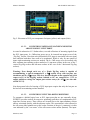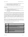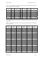
1
User’s Manual
Model XLMXXV
Universal Logic Module
For VME Systems
JTEC Instruments
32 Thompson Rd.
Rochester, NY, USA
Tel: (585)-334-7215
http://www.jtec-instruments.com
Information furnished by JTEC Instruments (JTEC) is believed to be accurate and reliable. However,
no responsibility is assumed by JTEC for its use, nor for any infringements of patents or other rights
of third parties, which may result from its use. No license is granted by implication or otherwise under
any patent or patents rights of JTEC. JTEC reserves the right to change specifications at any time
without notice.
Copyright 2004 by JTEC
Manual #: mdo-XLMXXV-MAN-001.1
September 2004
Manual: XLMXXV
mdo-XLMXXV-MAN-001.0
TABLE OF CONTENTS
1.
OVERVIEW........................................................................................................................................... 3
1.1. SUMMARY OF FEATURES ........................................................................................................ 3
1.2. POSSIBLE APPLICATIONS ........................................................................................................ 4
2. SPECIFICATIONS ................................................................................................................................ 4
3. ARCHITECTURE.................................................................................................................................. 6
3.1. DEVICES ....................................................................................................................................... 6
3.1.1.
ASYNCHRONOUS STATIC RANDOM ACCESS MEMORY ........................................... 7
3.1.2.
FIELD PROGRAMMABLE GATE ARRAY........................................................................ 7
3.1.3.
DIGITAL SIGNAL PROCESSOR......................................................................................... 7
3.1.4.
VMEBUS INTERFACE AND BUS ROUTER/ARBITER ................................................... 8
3.1.5.
FLASH MEMORY................................................................................................................. 8
3.1.6.
ECL PORTS ........................................................................................................................... 8
3.1.7.
DIAGNOSTIC LEDs.............................................................................................................. 8
3.2. BUSES............................................................................................................................................ 9
3.2.1.
INTERFACE-TO-ASRAM BUSES....................................................................................... 9
3.2.2.
INTERFACE-TO-FPGA BUS ............................................................................................... 9
3.2.3.
INTERFACE-TO-DSP BUS .................................................................................................. 9
3.2.4.
INTERFACE-TO-HPI BUS ................................................................................................... 9
3.2.5.
BUS ARBITRATION SCHEME ........................................................................................... 9
3.2.6.
INHIBIT OF BUS ACCESS BY FPGA AND DSP ............................................................. 10
3.3. VMEBus ADDRESS SPACE....................................................................................................... 10
4. OPERATING INSTRUCTIONS.......................................................................................................... 11
4.1. HARDWARE SETUP.................................................................................................................. 11
4.1.1.
IMPORTANT WARNINGS ................................................................................................ 11
4.1.2.
CONFIGURING ECL PORTS............................................................................................. 12
4.1.3.
JUMPER SETTINGS ........................................................................................................... 14
4.2. ADDRESSING AND DATA FORMATTING CONVENTIONS ............................................... 15
4.2.1.
BIT NUMBERING IN ADDRESS AND DATA WORDS ................................................. 15
4.2.2.
ADDRESS REPRESENTATION ........................................................................................ 15
4.2.3.
ENDIANNESS ..................................................................................................................... 16
4.3. SOFTWARE ACCESS OF INTERNAL DEVICES.................................................................... 16
4.3.1.
ACCESSING INTERFACE REGISTERS ........................................................................... 16
4.3.2.
ACCESSING ASRAMs ....................................................................................................... 19
4.3.3.
ACCESSING FPGA............................................................................................................. 20
4.3.4.
ACCESSING DSP................................................................................................................ 20
4.4. PROGRAMMING OF THE USER FPGA................................................................................... 20
4.4.1.
ECL PORTS ......................................................................................................................... 20
4.4.2.
LED PORTS ......................................................................................................................... 22
4.4.3.
DSP INTERRUPT PORTS................................................................................................... 22
4.4.4.
INTERFACE PORTS........................................................................................................... 23
4.4.5.
CONFIGURING FPGA........................................................................................................ 28
4.5. USING THE DSP......................................................................................................................... 30
4.5.1.
DSP ADDRESS SPACE ...................................................................................................... 30
4.5.2.
USER’S GUIDE TO HOST-PROCESSOR INTERFACE .................................................. 30
4.5.3.
THE DSP BOOT PROCESS ................................................................................................ 32
4.6. The INTERRUPT SYSTEM OF XLMXXV................................................................................ 33
4.6.1.
WRITING TO IRQMail REGISTERS ................................................................................. 34
4.6.2.
ISSUING OF SERVICE REQUESTS.................................................................................. 34
4.6.3.
SETTING OF THE IRQPENDING FLAGS........................................................................ 35
4.6.4.
READING THE CONTENT OF THE IRQMAIL REGISTERS ......................................... 35
4.6.5.
CLEARING THE CONTENT OF THE IRQMAIL REGISTERS....................................... 35
4.6.6.
INSPECTING THE IRQPENDING FLAGS ....................................................................... 36
4.7. OPERATIONS ON THE FLASH MEMORY ............................................................................. 36
4.7.1.
FPGA UTILITY CONFIGURATION.................................................................................. 36
March 24, 2004
Page 1
Manual: XLMXXV
5.
mdo-XLMXXV-MAN-001.0
APPENDICES...................................................................................................................................... 38
5.1. USER CONSTRAINTS FILE, UCF ............................................................................................ 38
5.2. USING UTILITY CONFIGURATION OF FPGA ...................................................................... 42
5.2.1.
WRITING TO THE IRQ MAILBOX OF INTERFACE...................................................... 43
5.2.2.
TEST DATA PATTERNS ................................................................................................... 43
March 24, 2004
Page 2
Manual: XLMXXV
mdo-XLMXXV-MAN-001.0
JTEC Model XLMXXV
Universal Logic Module
1. OVERVIEW
JTEC Model XLMXXV is a highly versatile, general-purpose, programmable
universal logic module for use in VME-based systems. The desired logic
operations are performed by a Xilinx Virtex series Field Programmable Gate
Array (FPGA), while more elaborate numeric operations are performed by a
Texas Instruments 900-Mflops/s floating-point Digital Signal Processor (DSP)
TMS320C6711. XLMXXV is a derivative of XLM72V, with most of ECLTTL translators and I/O headers being replaced by a 120-pin mezzanine
connector. It is, thus, intended for use with custom mezzanine boards offering
a high degree of flexibility in I/O electric standards, including analog I/Os.
On the other end, XLMXXV communicates with computers via the VMEBus,
utilizing 32-bit addressing and 32-bit and 16-bit data transfer, including 32-bit
block transfer at rates of up to 40 Mbytes/s. Further, XLMXXV features two
banks of fast asynchronous static random access memory (ASRAM), 2 Mbytes
each, accessible to VMEBus, FPGA, and DSP, and it features an on-board 2
Mbyte EEPROM or flash memory allowing one to store up four FPGA
configuration files.
Few digital applications are out of XLMXXV range.
1.1. SUMMARY OF FEATURES
•
•
•
•
•
•
One 120-pin and one 60-pin mezzanine connector, accepting mezzanine
I/O boards.
Optional 16 front-panel ECL ports, substituting the 60-pin mezzanine
connector, configurable in quartets as either inputs or, with some
exceptions, as outputs, organized in one 34-pin and one 8-pin headers.
Three ports can be configured as external clock ports supporting rates of up
to 110 MHz. The clock ports are inputs only.
One user-programmable FPGA, XCV(50-300)-PQ240 by Xilinx, Inc.
One user-programmable, floating point DSP, TMS320C6711 by Texas
instruments, rated at 900 Mflops/s.
2 banks of fast asynchronous SRAM, 2 Mbytes each, addressable in 32-bit,
16-bit and 8-bit words.
A custom, programmable, in-system reconfigurable VMEBus interface and
bus router/arbitrator.
March 24, 2004
Page 3
Manual: XLMXXV
•
•
mdo-XLMXXV-MAN-001.0
One 4-Mbyte programmable erasable read-only memory holding up to two
FPGA configuration files.
Four front-panel LEDs, one indicating VMEBus operation and the
remaining three being user-programmable, mapped onto ports of the user
FPGA.
1.2. POSSIBLE APPLICATIONS
•
•
•
•
•
•
•
Wave-form digitizer, when used in conjunction with an optional mezzanine board
Intelligent Data Buffer
Scalers, Prescalers, Coincidence Registers, Time Stampers
Multilevel Trigger Logics
Digital Delay and Gate Generators
Detector Readout Processor
Histogramming Memory
Due to the ultimate parallelism of an FPGA, XLMXXV can be programmed to perform
multiple functions simultaneously, whether related or completely unrelated. For example,
part of XLMXXV may be programmed to function as a wave-form digitizer, while other
parts execute trigger logic, yet another parts serving as a block of gated and non-gated
scalers, and yet another part serving as digital delay and gate generators.
2. SPECIFICATIONS
Formfactor: 6U VME.
PC Board: 8-layer, double-sided mixed surface-mount and through-hole.
VME Connectors: 96-pin J1, J2, and 30-pin JAUX implementing CERN extensions.
Optional ECL Ports: 16, mapped onto the user FPGA.
Mezzanine Connectors: one 120-pin and one 60-pin, the latter replacing the optional
ECL ports
LEDs: one to indicate VMEBus operations, three user-programmable, via the FPGA
configuration.
Clocks: one 80 MHz - shared by the VMEBus interface and FPGA; one 37.5 MHz for
DSP.
External Clock Inputs: up to three, rated at 110 MHz.
March 24, 2004
Page 4
Manual: XLMXXV
mdo-XLMXXV-MAN-001.0
FPGA: Virtex series XCV(50-300) by Xilinx.
DSP: TMS320C6711 by Texas Instruments.
ASRAMs: 16 CY7C1024B-15CV, organized in two banks of 2-Mbyte 32-bit memory.
FPGA Configuration Memory: 4-Mbyte AT29C040A by Atmel.
VMEBus Addressing: 32-bit, geographic.
VMEBus Data Transfer: 32-bit and 16-bit; 32-bit block transfer at rates of up to 40
Mbytes/s.
Front Panel: Black, anodized, with white silk-screen labeling; two ejector handles with
anodized blue ID plates.
Power Requirements: +5V at approximately 1.5 A; -5.2V at approximately 600 mA;
-2V at approximately 100 mA. Depends on ECL port usage.
March 24, 2004
Page 5
Manual: XLMXXV
mdo-XLMXXV-MAN-001.0
3. ARCHITECTURE
XLMXXV features a number of distinct devices, interconnected by address, data, and
control buses in star-like topology. Two devices, the FPGA and the DSP may serve,
along with the VMEBus, as bus masters, assuming and releasing control of the buses
according to user-programmable routines. A block-diagram of XLMXXV is illustrated in
Fig. 1.
Fig. 1. Block-diagram of XLMXXV.
Interaction of devices and routing of buses is discussed in Sections 3.1 and 3.2, further
below.
3.1. DEVICES
XLMXXV features eight distinct devices, five of which are addressable via VMEBus.
The addressable devices include:
(i, ii) two banks of fast asynchronous static random access memories (ASRAM),
(iii) one Field-Programmable Gate Array (FPGA),
(iv) one floating-point digital signal processor (DSP) (more accurately, the host
processor interface, HPI, of this processor), and
March 24, 2004
Page 6
Manual: XLMXXV
mdo-XLMXXV-MAN-001.0
(v) a VMEbus Interface and Bus Arbiter/Router Array (Interface).
The non-addressable (by VMEBus) devices are accessible to the user FPGA and include:
(vi) one flash memory to store configuration data for the FPGA,
(vii) an array of 72 ECL ports, and
(viii) an array of four front-panel diagnostic light-emitting diodes.
3.1.1.
ASYNCHRONOUS STATIC RANDOM ACCESS
MEMORY
XLMXXV features two banks of fast asynchronous static random access memory,
referred to as ASRAM A and ASRAM B. Both banks are identical and consist of four
CY7C1024B-15VC ICs manufactured by Cypress Semiconductor, Inc., providing for 2
Mbytes of storage capacity, each. They are configured as 32-bit wide memory, but can be
also accessed in half-words by both, VMEBus and by the DSP, and by half-words and
byte-wise by the FPGA.
3.1.2.
FIELD PROGRAMMABLE GATE ARRAY
The desired logical operations of XLMXXV are to be programmed by the user into a
Xilinx XCV(50-300)-PQ240C field programmable gate array chip (FPGA). Any logic
that can be implemented as synchronous state machine or combinatorial equation may be
programmed, subject only to the availability of resources of the Virtex series XCV* chip,
which are quite vast. For an XCV300, these resources include, among other things:
(i)
(ii)
(iii)
(iv)
(v)
6912 logic cells,
322,970 system gates,
1536 complex logic blocks,
65,536 block RAM bits, and
Built-in clock-management circuitry with four DLLs.
The FPGA is clocked at 80 MHz from an on-board clock, but can be also clocked
externally via one of four special ECL ports at rates of up to 110 MHz. The FPGA
features DLLs, which can be used to double the internal clock rate.
The FPGA can access Interface registers, and both banks of ASRAM. Further, it has
exclusive control of Flash Memory, of all ECL ports, and of three out of four front-panel
diagnostic LEDs.
3.1.3.
DIGITAL SIGNAL PROCESSOR
To allow one to perform more complex numerical operations on data that are beyond the
capabilities of the user FPGA, XLMXXV is equipped with a Texas Instruments
TMS320C6711 floating-point digital signal processor. The processor is clocked at 150
March 24, 2004
Page 7
Manual: XLMXXV
mdo-XLMXXV-MAN-001.0
MHz and, given its 6 parallel processors, is rated at 900 Mflop/s. The DSP can access
select registers of the Interface and both banks of ASRAM, in either 32-bit data words or
in 16-bit words. VMEBus can access the DSP via the Host Port Interface (HPI) of the
latter.
3.1.4.
VMEBUS INTERFACE AND BUS ROUTER/ARBITER
The communication between VMEBus and various devices of XLMXXV is mediated by
an interface and bus router/arbiter array implemented in four Xilinx Complex
Programmable Logic Devices (Interface). The Interface is comprised of one XC9521610PQ160C and three XC95288XL-7TQ144C chips. Individual CPLDs can be
reprogrammed in-system via the on-board JTAG port, allowing one to alter the
functionality of the Interface should a need arise. The Interface serves also as a multiplemaster bus router and arbiter, such that it may route in parallel bus needs by more than
one master. Since XLMXXV features three masters, VMEBus, FPGA, and DSP, there is
a need not only for bus routing but also for bus arbitration. The needed arbitration scheme
is also implemented in the Interface array.
Furthermore, some of the registers of the Interface serve the role of mailboxes for
sending messages between the VMEBus, DSP, and the FPGA. In particular, such
registers are used to implement interrupt and polling schemes required by various data
acquisition systems.
3.1.5.
FLASH MEMORY
To provide for the storage of the FPGA configuration data, XLMXXV is equipped with
one 4 MBit Programmable Erasable Read-Only Memory (Flash Memory), an ATMEL
AT29C040A. The size of this memory is sufficient to accommodate up to two
configuration files, one of which is a default boot configuration. The Flash Memory is
socketed, but can be reprogrammed in system. The chip is rated for 10,000 programming
cycles and 20-year data retention.
3.1.6.
ECL PORTS
XLMXXV is equipped with 72 ECL ports organized in four 34-pin and one 8-pin header.
The ports are controlled exclusively by the FPGA and can be configured in quartets as
either inputs or outputs, but always unidirectional. Four ECL ports serve special role, as
they are associated with clock inputs of the FPGA. As such they can serve as inputs for
external clock signals to the FPGA.
3.1.7.
DIAGNOSTIC LEDs
XLMXXV is equipped with four front-panel light-emitting diodes (LED), one of which
(yellow) signals VMEBus operations by the Interface and the remaining three (red, green,
and yellow) being controlled by the FPGA and, hence, by the user configuration. Every
March 24, 2004
Page 8
Manual: XLMXXV
mdo-XLMXXV-MAN-001.0
LED is driven via a pulse-length extender such that even short, 20ns-long pulses produce
robust flashes, while long pulses or DC levels are transmitted to the LED unaltered.
3.2. BUSES
Devices of XLMXXV and the VMEBus communicate with each other via the VMEBus
and five internal buses. All communications are mediated by the Interface, which routes
addresses and data generated by the three masters, VMEBus, FPGA, and DSP, to the
respective target devices. The Interface allows for a concurrent access of several buses by
several masters and performs at the same time the function of the bus arbitrator.
3.2.1.
INTERFACE-TO-ASRAM BUSES
The two ASRAMs, ASRAM A and ASRAM B, communicate with the Interface via their
respective buses, named Bus A and Bus B, respectively. Each of these buses has 19
address, 32 data, and 3 control lines. Bus A is shared with the Flash Memory, with the
exception of one control line, for which the Flash Memory has its individual counterpart.
Buses A and B can be controlled, by any of the three masters, VMEBus, FPGA, and
DSP. Which, in practical terms, means that any one of these three masters can write to or
read from either of the two banks of ASRAMs.
3.2.2.
INTERFACE-TO-FPGA BUS
The FPGA communicates with the Interface via a bus named Bus X, featuring 19
address, 32 data, and 26 control lines. Bus X can be controlled by either the VMEBus or
the FPGA.
3.2.3.
INTERFACE-TO-DSP BUS
The DSP communicates with the Interface via a bus named Bus D, featuring 19 address,
32 data, and 11 control lines. Bus D is controlled exclusively by the DSP.
3.2.4.
INTERFACE-TO-HPI BUS
The Host Processor Interface (HPI) of the DSP communicates with the Interface via a bus
named Bus H, featuring 16 data and 7 control lines. Bus H is controlled exclusively by
the VMEBus.
3.2.5.
BUS ARBITRATION SCHEME
Buses A, B, and X can be controlled by more than one master and, consequently, an
arbitration scheme is provided by the Interface to guarantee each of the three masters, the
March 24, 2004
Page 9
Manual: XLMXXV
mdo-XLMXXV-MAN-001.0
VMEBus, FPGA, and DSP access to these buses, while avoiding bus contention. The
arbitration scheme is based on the “first-come-first-serve-release-when-done” principle,
whereby the masters are granted control of buses on first-come-first-serve principle and
are required to release the control upon completion of their task.
Masters post their bus requests in the respective bus request registers of the Interface. The
requests are placed on the queues associated with individual buses and are granted as
soon as the bus involved becomes available. The grant of the bus control is signaled to
the requesting master by the content of the respective bus grant register. The requesting
master, upon detection of the bus grant signal, takes control of the bus, performs the
intended task, and removes its request from the request register, making the bus available
to the master that is first in the queue.
3.2.6.
INHIBIT OF BUS ACCESS BY FPGA AND DSP
The Interface provides the VMEBus with the capability to inhibit the control of buses by
the remaining two masters, the FPGA and the DSP. In other words, the VMEBus can, at
will, “snatch” the bus control already in progress from the FPGA and/or DSP, so as to
allow it to perform urgent or emergency tasks of its own. The response of the FPGA and
the DSP to the bus “snatching” is at the discretion of the user and is to be programmed
into the FPGA and the DSP, respectively. A reasonable programming is assumed to
detect the occurrence of “snatching” and provide for its smooth handling, e.g., the
abortion of the current operation and release of the request or, when feasible, suspension
of the current operation and its resumption upon removal of the bus grant inhibit.
3.3. VMEBus ADDRESS SPACE
The address spaces of the five addressable devices of XLMXXV are defined by 24 bits,
A0 – A23 of the complete VMEbus address, bits A24 - A26 being disregarded and bits
A27 - A31 carrying the geographical address of XLMXXV.
ASRAM A
ASRAM B
FPGA
DSP/HPI
INTERFACE
March 24, 2004
000000h - 1FFFFCh
200000h - 3FFFFCh
400000h - 5FFFFCh, used freely at user’s discretion
600000h - 7FFFFCh, most of which is unused
800000h – 9FFFFCh, most of which is unused
Page 10
Manual: XLMXXV
mdo-XLMXXV-MAN-001.0
4. OPERATING INSTRUCTIONS
Successful operation of XLMXXV requires its proper hardware setup, the programming
of its user FPGA and/or DSP, and the computer-access of its five addressable devices via
VMEBus.
4.1. HARDWARE SETUP
The hardware setup of XLMXXV includes (i) configuring its front-panel ECL ports for
operation in conjunction with the intended FPGA configuration and (ii) making sure that
the three blocks of jumpers, JP34 – JP36 are configured properly. Furthermore, one is
expected to connect respective ECL ports to external devices with twisted-pair or flat
ribbon cables. The ECL ports are configurable in quartets either as inputs or outputs. The
four ports identified by silk-screen labels (on the front panel and on the XLMXXV board)
as E1-E4 play a special role as they connect via ECL-to-TTL translators (MC10125) to
primary (PGCK) clock inputs (E1-E3) and secondary (SGCK) inputs (E4) of FPGA.
These FPGA inputs can be used to drive intrinsic clock nets of FPGA. Accordingly, ports
E1-E4 can and should be used to supply external clock signals, up to 110 MHz, to
XLMXXV.
4.1.1.
IMPORTANT WARNINGS
Improper configuration of ECL ports may lead to the damage of translator ICs or a costly
damage of the XLMXXV board or of the user FPGA. A special care should be taken to
correctly identify and populate the sockets with translator ICs. When not sure, please
consult JTEC Support service.
Warning 1: Only one translator IC (either input or output) is allowed for any single
port. Which, in practical terms, means that in any horizontal pair of sockets at most
one should be filled.
Warning 2: When configuring input ports (MC10125), it must be ascertained that
the corresponding ports of the FPGA are configured, indeed, as input ports and not
as output ports. In particular, this applies to the default “boot” configuration of the
FPGA active upon power-up.
To avoid ports conflict right upon power-up, it is recommended to keep as the default
“boot” configuration the general Utility Configuration supplied originally with
XLMXXV, or its possible update. This Utility Configuration has no FPGA ports
configured as outputs and, hence, guarantees that there is no conflict with any translator
IC.
March 24, 2004
Page 11
Manual: XLMXXV
mdo-XLMXXV-MAN-001.0
Warning 3: XLMXXV requires differential ECL inputs and will not function
properly (no damage will occur, though) with single-ended ECL signals. Which
means, among other things, that these inputs cannot be driven by an ECL bus
connected to ECL outputs of multiple external devices.
Warning 4: When configuring output ports, make sure that the input-polarizing
resistor arrays for the particular quartets of ECL ports, are removed from their
respective sockets.
4.1.2.
CONFIGURING ECL PORTS
ECL-to-TTL conversion (input) and TTL-to-ECL conversion (output) is accomplished by
16-pin MC10125 and MC10124 ICs, respectively. Each converter IC is capable of
interfacing up to four differential ECL ports to respective four TTL ports of the user
FPGA. Differential inputs of these ICs are directly connected to respective pairs of pins
of front-panel headers. The headers are identified (going from top to bottom) by labels A,
B, C, D, and E, respectively while individual ports within a header are identified by
numbers 1 through 17 (ports A – D) or 1 through 4 (port E). It is important to note that
(as indicated on the front panel of XLMXXV) port 1 of each of the five headers is
represented by the bottom pair of pins of the header and, thus, for example, ports A1-A4
are the four bottom pairs of pins of the top-most 34-pin header.
As indicated by silk-screen labels printed right below each of the two columns of 18 16pin sockets, the input translators are to be placed into sockets in the right-most column
while the output translators are to be inserted into sockets of in the left-most column. The
correspondence between the sockets and the ECL ports is indicated by silk-screen labels
printed between the two columns of 16-pin sockets. Note that 17-th ports (top-most) of
headers A – D are associated with the pair of sockets labeled A17-D17 – 9-th pair from
top.
In addition to translator ICs, proper functioning of ECL ports requires either impedancematching resistor arrays of 8 x 50Ω (input ports) or pull-down resistor arrays of 8 x 470Ω
(output ports). These two types of arrays share “Zig-Zag” sockets, with the exception of
their first (common) pins, marked by dots. The correspondence between the ECL ports
and the (10-position) rows of the “Zig-Zag” sockets is indicated by silk-screen labels
printed on both sides of these sockets.
Figure 2 illustrates placement of translator chips and resistor arrays for ECL ports D1-D4
configured as output ports and ports E1-E4 as input ports. Dots indicate pins #1.
March 24, 2004
Page 12
Manual: XLMXXV
mdo-XLMXXV-MAN-001.0
Fig. 2. Placement of ECL port components for inputs (yellow) and outputs (blue).
4.1.2.1. CONFIGURING IMPEDANCE-MATCHING RESISTOR
ARRAYS FOR ECL INPUT PORTS
As noted in subsection 4.1.2 further above, to avoid reflections of incoming signals from
the ECL input ports, 8 x 50Ωresistor arrays are to be inserted into proper rows of the
“Zig-Zag” sockets. Note that each (differential) ECL input is associated with two signal
lines and that both these lines need to be terminated. Which is why for one quartet of
inputs eight terminating resistors are needed. The 8 x 50Ω arrays are to be inserted with
their common pins entering sockets marked as I1 (top-most sockets in the case of the 7
vertical Zig-Zag sockets and left-most sockets in the case of the 2 horizontal Zig-Zag
sockets).
Warning: Even though each row of a 20-pin Zig-Zag socket is capable of
accommodating a typical commercial 9 x 50Ω resistor array with ten pins, one
should use only 8 x 50Ω arrays. This is so, because the pins on the opposite end (with
respect to I1) of the Zig-Zag sockets, labeled as O1, are connected to –5.2V, to
supply pull-down voltage for output port resistor arrays (8 x 470Ω) (see also subsection 4.1.2.3).
Note that general rules for bussing of ECL input ports require that only the last port on
the bus has its terminating resistor installed.
4.1.2.2.
CONFIGURING INPUT POLARIZING RESISTORS
To guarantee a default logical zero at ECL input ports that are not externally driven,
XLMXXV provides sockets for respective polarizing (pull-down of complementary ECL
input line) resistor arrays. These sockets are located next to the input translator sockets
and are associated directly with the adjacent socket. This association is also reflected in
the silk-screen label printed next to the socket. Position of the pin 1 (common) is in this
case indicated by the “cut corner” of the silk-screen socket outline (bottom). The inputMarch 24, 2004
Page 13
Manual: XLMXXV
mdo-XLMXXV-MAN-001.0
polarizing resistors should be removed when the particular ports are configured as output
ports.
Note, that the use of polarizing resistors is not mandatory, unless the user configuration
of FPGA relies on a definite polarization. It may be, however, a sound practice to use
these resistors with every input translator.
Note that general rules for bussing of ECL input ports require that only the last port on
the bus has its polarizing resistor installed.
4.1.2.3.
CONFIGURING OUTPUT PULL-DOWN RESISTORS
For a proper operation of ECL output ports, 8 x 470Ω pull-down resistor arrays are to be
inserted into proper rows of the “Zig-Zag” sockets. Note that each (differential) ECL
output is associated with two signal lines and that both these lines need to be pulled
down, via resistors, to VEE=-5.2V. Which is why for one quartet of outputs, eight pulldown resistors are needed. The 8 x 470Ω arrays are to be inserted with their common
pins entering sockets marked as O1 (bottom sockets in the case of the 7 vertical Zig-Zag
sockets and right-most sockets in the case of the 2 horizontal Zig-Zag sockets).
Warning: Even though each row of a 20-pin Zig-Zag socket is capable of
accommodating a typical commercial 9 x 470Ω resistor array with ten pins, one
should use only 8 x 470Ω arrays. This is so, because the pins on the opposite end
(with respect to O1) of the Zig-Zag sockets, labeled as I1, are connected to ECL bias
voltage, to supply terminating voltage for input port resistor arrays (8 x 50Ω) (see
also sub-section 4.1.2.1).
Note that general rules for bussing of ECL output ports require that only the last port on
the bus has its pull-down resistor installed.
4.1.3.
JUMPER SETTINGS
There are three jumper blocks on the XLMXXV board that must be properly configured
for a normal operation of the module. These are the 3-pin JP34 on the top of the board
(front-panel facing left), the 6-pin JP35 close to the upper left corner of DSP
(TMS320C6711), and the 3-pin JP36 right below JP35.
4.1.3.1.
JP34 SETTINGS – FPGA DEFAULT BOOT SOURCE
JP34 has two positions identified by silk-screen labels “SPROM” and “JTAG”,
respectively. For normal operation, the jumper should be placed in the “SPROM”
position, i.e., connecting the two left-most pins of JP34. This allows FPGA to boot upon
power-up from the default “boot” sector of the flash memory (socketed AT29C040A to
the left of JP34). The “JTAG” position of JP34 is intended primarily for in-systemprogramming/reprogramming, in conjunction with the 6-pin JP33 JTAG header, of the
four complex programmable logical devices (CPLDs) constituting the Interface. Since the
March 24, 2004
Page 14
Manual: XLMXXV
mdo-XLMXXV-MAN-001.0
user FPGA is in a common JTAG chain with the Interface CPLDs, it can be programmed
via the JTAG port too, when JP34 is set to “JTAG”.
4.1.3.2.
JP35 SETTINGS – DSP BOOT SOURCE AND DATA SIZE
JP35 is used to select the boot source and the size of the boot data for DSP. It has three
pairs of pins, with one pair serving only as a storage bin. The significance of various
jumper settings is described by the silk-screen label located right to JP35. It is shown in
Table 1 below
Table 1. Settings of DSP boot mode jumpers.
1-2
OFF
ON
OFF
ON
4.1.3.3.
3-4
OFF
OFF
ON
ON
Boot Source/DataWord Size
ASRAM A/8-bits
ASRAM A/32-bits
HPI/16-bit (Default)
ASRAM A/16-bits
SETTINGS OF JP36 – DSP ENDIANNESS
JP36 selects endianness of DSP, as indicated by the silk-screen labels to its right. With a
jumper in the lower position “LE”, DSP operates in little-endian, while with a jumper in
the upper position “BE”, DSP operates in big-endian.
4.2. ADDRESSING AND DATA FORMATTING
CONVENTIONS
Further below, the role of individual bits in various address and data words will be
discussed, as well as the significance of various addresses and values of data words
stored at these address locations. The rules adopted to identify individual bits and to
interpret address and data words are presented in sub-sections 4.2.1. – 4.2.3., below.
4.2.1.
BIT NUMBERING IN ADDRESS AND DATA WORDS
Whenever the role of individual bits, either in address or data words is discussed, it will
be assumed further below that the least significant bit has index zero. Accordingly, the
most significant bit in a 32-bit word is bit 31.
4.2.2.
ADDRESS REPRESENTATION
XLMXXV allows only 32-bit addressing, with the five most significant bits of this
address representing the slot number occupied by XLMXXV or, in other words, its
March 24, 2004
Page 15
Manual: XLMXXV
mdo-XLMXXV-MAN-001.0
geographic address. To address the total of five addressable internal devices, XLMXXV
implements a 24-bit scheme, where the 3 most significant bits identify the device of
interest and the remaining 21 bits identify the internal register or memory location of the
device. Note that 21 bits are needed to make use of the full capacity of individual
ASRAM banks. Therefore, further below, for the sake of simplicity, all addresses are
expressed in the form of 5-digit hexadecimal numbers, with a tacit understanding that a
full VMEBus address has always bits 24 through 26 set to zero and that bits 27 through
31 encode geographic address.
4.2.3.
ENDIANNESS
Endian is a term commonly used to describe the way multi-byte data words are stored in
memory. VMEBus is inherently big-endian, such that bytes of increasing hierarchy are
stored at memory locations of decreasing addresses. Which means that the most
significant byte of a multi-byte word is stored at lowest memory location and the least
significant byte at highest memory location. Accordingly, data bytes of highest
significance are transferred over VMEBus data lines of lower indices. And so, in 32 bit
transfers, the most significant byte is transferred over data lines D0-D7, the second most
significant byte, over data lines D8-D15, the second least significant byte, over data line
D16-D24, and the least significant byte, over data lines D25-D31. Similarly, in 16-bit
transfers, the most significant byte is transferred over data lines D0-D7 and the least
significant byte, over data lines D8-D15.
On the other hand, modern PC’s are mostly little-endian, such that higher hierarchy bytes
occupy higher memory locations. Also, modern VME crate controllers often offer the
capability of a fast hardware conversion between the big- and little-endian formats. With
this in mind, the present manual uses little-endian format, i.e., all data discussed further
below are represented in little endian format.
4.3. SOFTWARE ACCESS OF INTERNAL DEVICES
4.3.1.
ACCESSING INTERFACE REGISTERS
The use of the memory space of the Interface is fixed by the Interface firmware at the
design or upgrade time. The VMEbus must write to proper locations of this space to
accomplish the following tasks:
(i)
(ii)
(iii)
Request control of any of the three, shared internal buses that are subject to
bus arbitration, Bus A, Bus B, and Bus X (see also Section 3.2).
Issue interrupt signals to the DSP and FPGA and toggle reset lines for these
devices.
Write the interrupt request ID to the proper IRQ mailbox.
March 24, 2004
Page 16
Manual: XLMXXV
(iv)
(v)
(vi)
mdo-XLMXXV-MAN-001.0
Select the “warm” boot source for the FPGA, which is either one of the 4
banks of the Flash Memory, or ASRAM A (See also Section X).
Snatch the bus control from the FPGA and the DSP.
Reset the FPGA and DSP Interrupt Service Registers and Flags.
The VMEbus must read from proper locations of the address space to accomplish the
following tasks:
(i)
(ii)
(iii)
(iv)
Check if the requested control of any of the buses has been, indeed, granted.
Check what the actual FPGA boot source is.
Check the actual ownership of the three arbitrated buses.
Poll the Interrupt Service Registers of the FPGA and DSP for the presence of
service requests.
Addressing of the Interface registers may appear somewhat peculiar, due to the fact that
the Interface is implemented in four Complex Programmable Logical Devices (CPLDs),
each of which has access only to a portion (non-contiguous) of the VMEBbus address
bus. For example, the “Master” CPLD controlling the Interface logics has access only to
the VMEbus data lines D0, D1, D16, and D17, as well as to the address lines A1, A2, A3,
A16, and A17. Which is why, with few exceptions, accessing of the Interface is
accomplished over the data lines D0, D1, D16, and D17 and address lines A2, A3, A16,
and A17, accounting for the apparent peculiarity of the Interface addressing and data
scheme.
Addresses of the Interface registers are shown in Table 2 below. Note that bit 23 is
always set to “1”, to select the Interface as the target device. Note also that to form a
complete VMEbus address, the 24-bit addresses shown in Table 2, must be pre-pended
by a 5-bit geographical address, followed by three “don’t” care bits.
Table 2. Use of the Interface address space.
Address bits
A0-A23
800000h
800004h
800008h
80000Ch
810000h
810004h
810008h
820000h
820004h
820048h
820824h
821048h
March 24, 2004
Registers accessed or action induced
Bus control register and IRQ flags (write/read)
FPGA and DSP reset register (write-only)
FPGA boot source register (write/read)
Inhibit flag for the bus control by FPGA and DSP
Bus A ownership register (read-only)
Bus B ownership register (read-only)
Bus X ownership register (read-only)
Clear IRQ Mailboxes and the associated flags (write-only)
Interrupt FPGA (write-only)
Serial number (read-only)
Mailbox register (read-only)
DSP mailbox and interrupt (write-only)
Page 17
Manual: XLMXXV
mdo-XLMXXV-MAN-001.0
The significance of data written to or read from the valid locations of the Interface
address space is discussed in detail in sub-sections 4.3.1.1-4.3.1.9 below.
4.3.1.1.
BUS CONTROL REQUEST REGISTER AT 800000h
The bus control register located at 800000h is a 3-bit register mapped onto bits 0, 1, and
16 of the 32-bit VMEBus word. When set by a “Write” operation, they indicate to the bus
arbitrator the request by the VMEBus of the control of an arbitrated bus:
Request Bus A
Request Bus B
Request Bus X
Request Bus B for DSP
REQA = 00000001h
REQB = 00000002h
REQX = 00010000h
REQD = 00020000h
To release a bus, its respective request bit must be set to 0. Note that the Interface will
always simultaneously set and/or release requests of all three buses, depending on which
of the four bits, 0,1, 16, and 17 are set and which are reset.
Example: a combined request of all three buses of XLMXXV is achieved by writing
(REQA OR REQB OR REQX) = 00010003 to the address 800000. To release all these
three buses at the same time, one simply writes 0 to the same address.
4.3.1.2.
FPGA AND DSP RESET REGISTER AT 800004h
The FPGA and DSP reset register at 800004h is a 2-bit write-only register mapping onto
bits 0 and 1 of the 32-bit VMEBus word. Depending on what data are written into these
two bits, the Interface will set or release the reset signal of the FPGA or DSP. The action
is always simultaneous on both register bits involved.:
Set Reset for the FPGA
Set Reset for the DSP
RESFPGA = 00000001h
RESDSP
= 00000002h
Reset signals are released by setting the associated bits to 0.
Example:
To only set the Reset for the FPGA, one must write (RESFPGA OR RESDSP OR
IRQFPGA OR IRQDSP) = 1 to the memory location 800004. To release this reset one
writes 0 to this memory location. Note that the latter causes then the FPGA to boot from
the selected boot source.
4.3.1.3.
FPGA BOOT SOURCE SELECTOR REGISTER AT 800008
The FPGA boot source selector register is a write/read 4-bit register mapping onto bits 0,
1, 16, and 17 of the 32-bit VMEBus word:
March 24, 2004
Page 18
Manual: XLMXXV
mdo-XLMXXV-MAN-001.0
Select sector 0 of flash memory
Select sector 1 of flash memory
Select sector 2 of flash memory
Select sector 3 of flash memory
Select ASRAM A
BOOT0
BOOT1
BOOT2
BOOT3
BOOTA
=
=
=
=
=
00000000h
00000001h
00000002h
00000003h
00010000h
The BOOTA bit overrides the other BOOT bits that might be set.
Example:
To select ASRAM A as a boot source of the FPGA, one must write BOOTA=00010000h
to the memory location 800008.
4.3.1.4. BUS CONTROL INHIBIT FLAG FOR FPGA AND DSP AT
80000Ch
Writing “1” to 80000Ch inhibits bus control by the FPGA and DSP, and makes all buses
A, B, and X unconditionally available to the VMEBus. To actually gain the control of the
desired bus, VMEBus must still request control of the bus. Writing “0” to 80000Ch
removes inhibit and allows the FPGA and DSP to compete for the bus control.
4.3.1.5. BUS OWNERSHIP REGISTERS AT 810000h, 810004h, AND
810008h
Bus ownership registers at 810000h, 810004h, and 810008h are 2-bit read-only registers
storing data identifying the actual owner of Bus A, B, and X respectively. The returned
values of 0, 1, 2, and 3 indicate free status, and control by the VMEBus, FPGA, and DSP,
respectively.
4.3.1.6.
XLMXXV SERIAL NUMBER REGISTER AT 820048h
The serial number register at 820048h is an 11-bit read-only register storing the
XLMXXV serial number. This number is returned in bits 0 – 10 of the 32-bit data word.
4.3.1.7. INTERRUPT SYSTEM REGISTERS AT 820000h, 820004h,
820824h, AND 821048h
The significance and use of Interface addresses 820000h, 820004h, 820824h, and
821048h is discussed in detail in subsection 4.6.
4.3.2.
ACCESSING ASRAMs
One accesses either of the two ASRAMs by writing to or by reading from a desired
memory location mapped onto the respective VMEBus address space of the ASRAM of
March 24, 2004
Page 19
Manual: XLMXXV
mdo-XLMXXV-MAN-001.0
interest. As discussed in Section 3.3, the VMEBus address space for ASRAM A extends
from 0h to 1FFFFCh and that of ASRAM B, from 200000h to 3FFFFCh.
The use of the address spaces of the two banks of ASRAMs is straightforward and
involves writing of desired data into, or reading data from, the desired memory address.
For example, writing data to the address 000008h causes this data to be stored in the
memory location 8h of ASRAM A. As a second example, reading from memory location
200010h, will retrieve the content of the memory location 10h of ASRAM B.
4.3.3.
ACCESSING FPGA
The use of the address space of the FPGA remains at discretion of the user and is to be
determined at the design time of the user FPGA code. One would expect here only a few
low memory locations to be utilized with, perhaps, a suggestion to dedicate always the
same location 0 for storing a read-only 32-bit ID of the particular user firmware.
4.3.4.
ACCESSING DSP
The DSP can be accessed via its Host Port Interface (HPI) over the dedicated BUS H.
The use of this bus is described in detail in subsection 4.5.1.
4.4. PROGRAMMING OF THE USER FPGA
With Interface being an integral and tested part of XLMXXV, any further successful use
of XLMXXV hinges critically on the quality of the user code loaded into the FPGA of
XLMXXV. To write such a code, the user must know the role of all pins of the FPGA
used in the design of XLMXXV and must know or establish safe timing patterns for
interacting with other internal devices via write/read operations. The interaction
mechanism of the FPGA with other Devices is described in detail below.
4.4.1.
I/O PORTS
As described in Section 4.1, XLMXXV features a total of 89 I/O ports presented at one
120-pin (73 ports) and one 60-pin (16 ports) mezzanine connector. The latter mezzanine
connector can be replaced by 16 ECL ports.
For the actual numbers of the FPGA pins associated with pins of mezzanine connectors
and/or with the optional 16 ECL ports see Tables 3 and 3a, below and also Appendix A.
This appendix lists, with abundant comments, the relevant section of a user constraint file
(*.ucf) that can be used at the implementation time of the FPGA code. Note, that the user
has no particular interest in knowing the pin associations, as the UCF file takes care of
this task automatically, provided the design uses the proposed naming scheme.
March 24, 2004
Page 20
Manual: XLMXXV
mdo-XLMXXV-MAN-001.0
Table 3. Association between pins of the (60-pin) mezzanine connector B, optional ECL
ports, and physical FPGA pad numbers.
Mezz B
Pin
6
7
8
9
10
12
13
15
ECL
Port
A5
A4
A12
B1
A9
A8
A11
A10
FPGA
Pad #
199
200
188
187
192
193
189
191
Mezz. B
Pin
16
17
19
20
21
23
24
25
ECL
Port
A1
A7
A6
A3
A2
B4
B3
B2
FPGA
Pad #
203
194
195
201
202
213
210
92
Note, that FPGA pads 92, 210, and 213 are global clock pads and can, hence, be used
only as inputs.
Table 3a. Association between pins of the (120-pin) mezzanine connector A and physical
FPGA pad numbers.
Mezz. A
Pin
1
2
3
4
5
6
7
8
9
10
11
12
13
14
15
16
17
18
19
20
21
22
23
March 24, 2004
FPGA
Pad #
186
185
184
176
175
174
173
171
170
169
168
167
163
162
161
160
159
157
156
155
154
153
152
Mezz. A
Pin
26
27
28
29
30
31
32
33
34
35
36
37
38
39
40
41
42
43
44
47
48
49
50
FPGA
Pad #
146
145
144
142
141
140
139
138
134
133
132
131
130
128
127
126
125
124
100
108
109
118
117
Mezz. A
Pin
53
54
55
56
57
58
59
60
80
81
86
88
89
91
96
97
99
101
103
104
118
119
120
FPGA
Pad #
114
113
111
110
107
103
102
101
49
48
47
46
42
41
40
39
38
36
35
34
229
228
230
Page 21
Manual: XLMXXV
24
25
4.4.2.
mdo-XLMXXV-MAN-001.0
149
147
51
52
116
115
LED PORTS
XLMXXV3 is equipped with three front-panel user-programmable LEDs, red, green, and
yellow, controlled by FPGA configuration through expanding drivers. These drivers
extend the duration of short pulses (of at least 2 clock cycle duration) to approx. 25 ms to
provide for a robust flash of the associated LED, while not affecting the action of longer
pulses. All LED ports are active high. A non-configured FPGA will cause all three LEDs
to turn on – a state that can be taken as indicative of a failure of FPGA to boot.
Conversely, user LEDs will signal a successful configuration of the FPGA by displaying
a pattern foreseen by the user code.
In the UCF file (See Appendix 5.1) LED pads are named LEDOPD<1>-LEDOPD<3>,
respectively. Their association with physical pads of the FPGA is shown in Table 4.
Table 4. Front-panel LED control pads of the FPGA
LED
Red
FPGA
Pad #
99
4.4.3.
UCF Name of LED FPGA UCF Name of LED FPGA UCF Name of
FPGA Pad
Pad # FPGA Pad
Pad # FPGA Pad
LEDOPD<1> Green 97
LEDOPD<2> Yellow 96
LEDOPD<3>
DSP INTERRUPT PORTS
There are two lines connecting two pins of the FPGA to two interrupt pins of the DSP.
One of them (NMIDX) is used by the FPGA to drive the non-maskable interrupt NMI of
the DSP (pad C13 of the DSP), while the other one (INT6DX) drives the EXT_INT6 pad
D2 of the DSP. Both DSP interrupts are edge-driven by a low-to-high transition, with a
requirement for the level to be low for at least two system clock cycles and then high for
at least two cycles.
In the UCF file (see Appendix 5.1), the above two pins of the FPGA are labeled
NMIDXOPD and INT6DXOPD, respectively. Their association with physical pins of the
FPGA is shown in Table 5 below.
Table 5. DSP Interrupt pads of the FPGA
Interrupt
NMIDX
March 24, 2004
FPGA pin
205
Interrupt
INT6DX
FPGA pin
206
Page 22
Manual: XLMXXV
4.4.4.
mdo-XLMXXV-MAN-001.0
INTERFACE PORTS
With the exception of the two DSP interrupt signals discussed above, the FPGA
communicates with all internal devices, as well as with the VMEbus, via the Interface,
i.e., has direct connections only with pins of the constituent CPLDs of the Interface.
These are 19 local address lines, labeled in the UCF as LOCADPD<2>-LOCADPD<20>,
32 local data lines, labeled in the UCF as LOCDAPD<0>-LOCDAPD<31>, and 20
control lines supplying signals necessary for executing various operations. The address
and data signals, when accompanied by proper combination of control signals, propagate
via Interface to address and data pins of a desired ASRAM or Flash Memory, while the
Interface provides the output enable (OE) chip enable (CE), and write (WR) signals
necessary for accessing any device. It is important to appreciate that the local address and
data lines are bi-directional and, therefore, bi-directional pads and tri-state buffers must
be used by the FPGA to connect to these lines. It is then up to the user to provide for
proper enable signals for these buffers to achieve the desired result and, more
importantly, not to cause a prolonged bus contention.
4.4.4.1.
BUS ARBITRATION PORTS
Since internal devices of XLMXXV can be accessed by up to three different masters,
VMEbus, FPGA, and DSP, the presence of a reliable arbitration scheme is absolutely
necessary. The user FPGA code must comply with the simple rules of bus arbitration not
to cause prolonged bus contention that can lead to a destruction of components of
XLMXXV. The arbitration scheme of XLMXXV is based on the first-come-first-serverelease-when-done principle. Therefore, every access of any internal device of XLMXXV
by the FPGA (in fact, by any master) must be preceded by a request (issued to the
Interface) for exclusive control over the needed bus(es) followed by a verification that
such an access has been, indeed, granted. Naturally, grant of control over a bus to one
master automatically denies control over this bus to any competing masters. At the
conclusion of the access, the FPGA must remove the request, which releases the bus for
subsequent arbitration. There are three bus request lines associated with the three internal
buses subject to arbitration. These three buses are (i) Bus A, interconnecting Interface
and ASRAM A, (ii) Bus B, interconnecting Interface and Bus B, and (ii) Bus X,
interconnecting Interface and the FPGA. The bus interconnecting Interface and the DSP
is owned exclusively by the DSP and is, hence, not subject to arbitration. The bus request
signals are active low (so, a non-configured FPGA does not generate a false request).
With each of the three bus request lines associated is a respective bus grant signal, active
high. The bus grant signals are synchronized to the leading edge of the system clock. It is
absolutely essential that the user configuration of the FPGA conditions enabling of local
address lines of the FPGA by the presence of high on the Bus X grant line, as the
Interface cannot here provide protection from a contention on bus X. Also, the user
configuration must make sure that the local data buffers are not enabled when Interface is
writing into the FPGA registers.
Since the control of the FPGA over bus A or over bus B always involves its control also
over bus X, a request for bus X for the FPGA is generated automatically by the Interface
itself whenever the FPGA requests either bus A or bus B.
March 24, 2004
Page 23
Manual: XLMXXV
mdo-XLMXXV-MAN-001.0
In UCF (see Appendix 5.1), the bus A, B, and X request pads are labeled NREQAOPD,
NREQBOPD, and NREQXOPD, respectively, while the associated grant pins are labeled
ACKAIPD, ACKBIPD, and ACKXIPD. The association between the above arbitration
signals and the FPGA pad numbers is shown in Table 6 below.
Table 6. Bus arbitration pins of the FPGA
Bus Request
A
B
X
FPGA pin
56
64
72
4.4.4.2.
Bus Grant
A
B
X
FPGA pin
87
84
66
LOCAL ADDRESS PORTS
Local address lines are used to transmit address bits between the FPGA and the Interface,
under assumption that these address bits will propagate via the Interface to the target
device. The association between the local address bits and the FPGA pins is shown in
Table 7 below.
Table 7. Local Address pads of the FPGA
Address
bit
2
3
4
5
6
FPGA
Pad #
53
26
25
4
6
Address
bit
7
8
9
10
11
FPGA
Pad #
5
7
9
57
216
Address
bit
12
13
14
15
16
FPGA
Pad #
218
217
223
222
86
Address
bit
17
18
19
20
FPGA
Pad #
85
33
63
31
In UCF (see Appendix 5.1), local address pins are labeled LOCADPD<2>-<20>.
4.4.4.3.
LOCAL DATA PORTS
Local data lines are used to transmit data bits between the FPGA and the Interface, under
assumption that these data bits will propagate via the Interface to the target device. The
association between the local data lines and the FPGA pins is shown in Table 8 below.
March 24, 2004
Page 24
Manual: XLMXXV
mdo-XLMXXV-MAN-001.0
Table 8. Local Data pads of the FPGA
Data line
0
1
2
3
4
5
6
7
FPGA
Pad #
68
74
18
27
50
13
234
12
Data line FPGA
Pad #
8
232
9
11
10
21
11
236
12
208
13
235
14
224
15
220
Data line FPGA
Pad #
16
71
17
80
18
24
19
28
20
20
21
17
22
238
23
231
Data line FPGA
Pad #
24
3
25
10
26
23
27
237
28
207
29
215
30
209
31
221
In the UCF (see Appendix 5.1), local data pins are labeled LOCDAPD<0>-<31>.
4.4.4.4.
DATA BYTE ENABLE PORTS
While the data are addressed in XLMXXV in 32-bit words, there is a mechanism in place
that allows one to access any arbitrary combination of bytes, without affecting the
remaining bytes. One simply asserts a proper combination of data byte enable signals
(active low), NDBEO<0>-NDBEO<3>. Note that since the index 0 refers to low data
lines, it refers in fact to high data byte numbers (Big-Endian). For the most common and
fastest 32-bit data transfer, all four NDBEO<0>-NDBEO<3> signals may be set
permanently to 0, as they will be ultimately qualified within the Interface additionally by
an appropriate device select signal to be generated by the FPGA. In the UCF (see
Appendix 5.1), the data byte enable pins are labeled NDBEOPD<0>-NDBEOPD<3>.
The correspondence between these signals and FPGA pins is shown in Table 9.
Table 9. Data Byte Enable pins
Byte
0
FPGA pin
82
4.4.4.5.
Byte
1
FPGA pin
67
Byte
2
FPGA pin
73
Byte
3
FPGA pin
95
WRITE OPERATION PORTS
The FPGA signals to the Interface a write operation by asserting one or both of its
NWRA and NWRB lines (active low). NWRA low indicates that the operation upon
ASRAM A, the Interface, or the Flash Memory is a write operation. The target of the
operation is in this case determined by the Interface based on the state of the NSEL lines
discussed below. NWRA low indicates that the operation upon ASRAM B is a write
operation. Note that the two NWR signals are not strobes. They are to be asserted at the
time of the placement of the address and data on their respective local buses and de-
March 24, 2004
Page 25
Manual: XLMXXV
mdo-XLMXXV-MAN-001.0
asserted upon completion of operation. They should be kept constant for the duration of a
block transfer. In the UCF, the NWRA and NWRB pins are labeled NWRAOPD and
NWRBOPD, respectively. Their association with physical pins of the FPGA is shown in
Table 10 below.
Table 10. Write enable (output) pins of the FPGA
NWR signal
NWRA
4.4.4.6.
FPGA pin
81
NWR signal
NWRB
FPGA pin
70
DEVICE SELECTION PORTS
The FPGA signals to the Interface the intended target of its operation over three lines,
NSELA, NSELB, and NSELV, named in UCF as NSELAOPD, NSELBOPD, and
NSELVOPD. All these lines are active low and have dual functionality, depending on
whether the operation is “write” or “read”.
In write operations, NSEL signals serve as write strobes and, hence, must be asserted so
as to allow the address to propagate to the target device prior to their own reaching of the
target (via the Interface). It was found that a safe way to write to ASRAMs is to assert the
relevant NSEL signal for one system clock cycle, two system clock cycles after the
FPGA has placed the address and data on their respective local buses. In a block transfer,
this results then in a 3-cycle transfer and in an overall throughput of 107Mbyte/s (80MHz
clock). The Interface makes here use of the data byte enable signals (NDBEO<0>-<3>)
to strobe only the desired memory chips (storing individual bytes).
In read operations, NSEL signals serve as chip enable signals, which in conjunction with
the (ASRAM) output enable signals cause the target device to output the addressed data
on the data bus. In this case, NSEL is to be asserted at the time of the placement of
address on the local address bus and can be kept constantly low for the entire duration of
a block transfer. The ASRAM output enable signals are generated by the Interface when
the latter detects the presence of an NSEL signal in the absence of the associated NWR
signal (NWR high).
There are following valid combinations of the asserted NSEL signals:
(i)
(ii)
(iii)
(iv)
(v)
(vi)
NSELA alone,
NSELB alone,
NSELV alone,
NSELA and NSELV,
NSELA and NSELB, and
NSELA and NSELB and NSELV.
(i) and (ii) are used to achieve transfer of data between the FPGA and the individual
ASRAMs. (iii) is used to access the FPGA interrupt service register and the associated
March 24, 2004
Page 26
Manual: XLMXXV
mdo-XLMXXV-MAN-001.0
flag in Interface. The combination (iv) is used (e.g., by Utility Configuration) to write
data into the Flash Memory. The combination (v) allows simultaneous write by the FPGA
into both ASRAMS or a transfer of data between the two ASRAMs, while the
combination (vi) is intended for data transfer operations between ASRAM B and the
Flash Memory (programming of the Flash Memory with a configuration file stored in
ASRAM B or read-back of the content of the Flash Memory into ASRAM B). Note that
an access of the Flash Memory involves asserting both NSELA and NSELV. For
operations on the Flash Memory, the user is encouraged to use the default cold-boot
Utility Configuration residing in bank 0 of the Flash Memory.
Note that ASRAM A shares NWRA line and the Output Enable line with the Flash
Memory, which precludes transfer of data between ASRAM A and the Flash Memory.
These two devices have, however, separate chip enable signals, which allows one to
access any one of them individually.
The correspondence between the NSEL lines and the physical pins of the FPGA is shown
in Table 11.
Table 11. Device selection pins of the FPGA
Signal
NSELA
FPGA pin
93
4.4.4.7.
Signal
NSELB
FPGA pin
79
Signal
NSELV
FPGA pin
54
INTERRUPT PORTS
There are three “interrupt” lines interconnecting the FPGA and the Interface, one
dedicated for transmitting interrupt signals sent from the VMEbus to the FPGA
(NIRQXV), one for transmitting interrupt signals sent from the FPGA to the VMEbus
(NIRQVX), and one for transmitting interrupt signals sent by the DSP to the FPGA
(NIRQXD). The NIRQVX interrupt is not used in the present implementation of the
Interface.
In the UCF, the NIRQXV, NIRQVX, and NIRQXD pins are labeled NIRQXVIPD,
NIRQVXOPD, and NIRQXDIPD, respectively.
The association between the NIRQ signals and the physical pins of the FPGA is shown in
Table 12.
Table 12. Interrupt pins of the FPGA
IRQ
NIRQXV
March 24, 2004
FPGA pin
55
IRQ
NIRQVX
FPGA pin
78
IRQ
NIRQXD
FPGA pin
94
Page 27
Manual: XLMXXV
mdo-XLMXXV-MAN-001.0
4.4.4.8.
WRITE/READ CONTROL PORTS
The Interface controls writing and reading of data into/from the FPGA registers by means
of two signals NSELXV and NWRX. The mechanism is here very much the same as the
one used by the FPGA to execute read and write operations.
In a write operation NWRX is low for the duration of the operation (e.g., for the duration
of block transfer), while the NSELXV (active low) plays a role of the write strobe. User
configuration may then utilize the leading edge of the NSELXV to register the local data
LOCDA0-31 into registers identified by the local address LOCAD2-20.
In read operations, NWRX is high and NSELX is low for the duration of the operation.
User configuration must then respond by placing the content of the addressed register on
the local data bus and enabling the associated tri-state drivers. In this case, it is the
Interface that is in control of the timing.
In UCF, the NWRX and NSELX pads are named NWRXIPD and NSELXIPD,
respectively. Their association with physical pins of the FPGA is shown in Table 13
below.
Table 13. Write/read to/from FPGA control pads
Control line
NWRX
4.4.5.
FPGA Pad #
52
Control line
NSELX
FPGA Pad #
65
CONFIGURING FPGA
XLMXXV offers three ways of configuring FPGA:
(i)
(ii)
(iii)
via the JTAG port (see Section 4.1.3.1),
from Flash Memory, and
from ASRAM A.
Programming via the JTAG port is intended primarily for debugging purposes and
requires dedicated equipment (software and download cable) and, therefore, is not
discussed in this manual.
4.4.5.1.
CONFIGURATION DATA FILE
When configuring FPGA from ASRAM A or programming Flash Memory, a properly
formatted configuration data file is needed. FPGA programming software allows one to
generate binary configuration data as an array of 8-bit words. These 8-bit data words
have to be properly mapped onto 32-bit words to be loaded into ASRAM A or ASRAM
B (in the case of Flash Memory programming – see Section 4.5). The mapping is shown
in Table 14 below.
March 24, 2004
Page 28
Manual: XLMXXV
mdo-XLMXXV-MAN-001.0
Table 14. Mapping of 8-bit “raw” configuration data bytes onto 32-bit words
Bit # in “Raw” 8-bit Word
Bit # in 32-bit “XLM” Word
0
2
1
3
2
4
3 4 5 6 7
10 18 19 20 26
Note that a “raw” byte FFh converts to a 32-bit 41C041Ch “XLM” configuration word.
Furthermore, the header part of the “raw” data file has to be skipped and only the
configuration data proper converted and loaded into target ASRAM. To perform this
stripping, one has to rely on the fact that the first data word to be converted is FFh
(decimal 255), which means that a conversion program must skip all bytes read from a
“raw” configuration file until it encounters FFh (255). Note also that second valid byte is
always 0.
4.4.5.2.
CONFIGURING FPGA FROM FLASH MEMORY
Upon power-up, FPGA attempts to boot (configure itself) from the default, “boot” sector
of Flash Memory. Whether such a boot is successful or unsuccessful, one may force
FPGA to boot from a desired different sector of Flash Memory. To this end, one must:
(i)
(ii)
(iii)
select the desired boot sector by writing its ID (0 – 1, for the two sectors
available) into location 800008h (see Section 4.3.1.3),
set reset for FPGA by writing 1 into location 800004h (Section 4.3.1.2) , and
release reset for FPGA by writing 0 into location 800004h (Section 4.3.1.2).
Upon release of reset, FPGA will attempt to boot from the selected sector of Flash
Memory.
4.4.5.3.
CONFIGURING FPGA FROM ASRAM A
To reconfigure FPGA from ASRAM A, one must:
(i)
(ii)
(iii)
(iv)
(v)
(vi)
select ASRAM A as the FPGA boot source by writing 10000h into location
800008h (Section 4.3.1.3),
acquire control of Bus A by writing 1 into 800000h (Section 4.3.1.1)
load the desired configuration file into ASRAM A
release control of Bus A by writing 0 into 800000h (Section 4.3.1.1)
set reset for FPGA by writing 1 into location 800004h (Section 4.3.1.2) , and
release reset for FPGA by writing 0 into location 800004h (Section 4.3.1.2).
Upon release of reset, FPGA will attempt to boot from ASRAM A.
The above procedure has to be somewhat altered when FPGA is not yet configured. In
such a case, in order to be able to acquire Bus A, one must first inhibit the bus access by
FPGA and DSP by writing 1 into location 80000Ch (see Section 4.3.1.4) and then set
March 24, 2004
Page 29
Manual: XLMXXV
mdo-XLMXXV-MAN-001.0
reset for FPGA as in (v) above. Subsequently, one would have to perform (i), (ii), (iii),
(vi), and cancel inhibition of bus access by FPGA (by writing 0 into 80000Ch).
4.5. USING THE DSP
To use the DSP, the user must prepare an executable suitable for downloading into the
DSP and boot the DSP with this executable.
4.5.1.
DSP ADDRESS SPACE
The TMS320C6711 DSP has a single 32-bit address space covering internal memory and
registers, as well as external memories. The DSP accesses external memories through its
Extended Memory Interface (EMIF), capable of handling a variety of memory types. In
the XLMXXV, these external memories are the two banks of ASRAMs and the Interface,
all of which present themselves to the DSP as asynchronous random access memories.
The address space of the DSP is allocated as follows:
0000 0000h
Internal memory of the DSP
8000 0000h
ASRAM A (2 Mbytes)
9000 0000h
ASRAM B (2 Mbytes)
A000 0000h
Interface (few selected addresses)
By default the Extended Memory Interface is set for asynchronous RAM and, hence, will
work with ASRAMs and the Interface of XLMXXV. The default timing of the EMIF is,
however, slow and it is advisable to set it to a much faster one. The EMIF for any
particular internal device of XLMXXV can be configured by writing to the respective
EMIF register. The EMIF registers have the following addresses within the DSP internal
address space:
180 0008h
180 0004h
180 0010h
180 0000h
4.5.2.
EMIF for ASRAM A
EMIF for ASRAM B
EMIF for Interface
Global EMIF register
USER’S GUIDE TO HOST-PROCESSOR INTERFACE
General remarks:
(i)
The present guide applies to XLMXXVs equipped with DSPs with silicon ID
C21 and not C13 used in prototype series.
(ii)
XLMXXV powers up with DSP kept in reset state. To use HPI (and the DSP
in general) the reset must be removed by writing 0 to VMEBus address
800004h. Note that writing 2 to 800004h sets the DSP reset.
(iii)
By default, XLMXXV powers up with DSP boot mode set to HPI, regardless
of the setting of DSP boot mode jumpers.
March 24, 2004
Page 30
Manual: XLMXXV
mdo-XLMXXV-MAN-001.0
XLMXXV is designed to take advantage of the Host-Port Interface (HPI) of the
TMS320C6711 Digital Signal Processor. Via the HPI, the XLMXXV user has access to
internal registers of the DSP, as well as to the whole address space. The latter includes
internal devices of XLMXXV, such as Interface, ASRAM A, and ASRAM B.
Communication with HPI occurs through writing and reading to control (HPC), address
(HPA), and data (HPD) registers of the DSP using part of the HPI address space set up in
the Interface. The target register and the direction of transfer (read/write) are selected
using 4 VMEBus address lines – A2-A4 and A10 (A0 being the least significant bit).
These address lines connect (via Interface) to the HHWIL (Half-word Identification
Select), HCTL[1:0] (Access Control Select), and HRW (Read/Write Select) pins of the
DSP, as follows:
DSP Pin
HHWIL
HCTL[0]
HCTL[1]
VME
A2
A3
A4
HRW
A10
HHWIL=0 selects the first (16-bit) halfword
HCTL=0 selects HPC, HCTL=1 selects HPA,
HCTL=2/3 select HPD with/without address autoincrement
HRW=0/1 correspond to “Write”/”Read”
According to the above assignment, HPI maps onto VMEBus address space as follows:
VMEBus Address
600000h
600004h
600400h
600404h
600008h
60000Ch
600408h
60040Ch
600010h
600014h
600410h
600414h
600018h
60001Ch
600418h
60041Ch
HPI Function
Write first half-word into HPC
Write second half-word into HPC
Read first half-word from HPC
Read second half-word from HPC
Write first half-word into HPA
Write second half-word into HPA
Read first half-word from HPA
Read second half-word from HPA
Write first half-word into HPD, with addr. autoincr.
Write second half-word into HPD, with addr. Autoincr.
Read first half-word from HPD, with addr. autoincr.
Read second half-word from HPD, with addr. Autoincr.
Write first half-word into HPD, fixed address
Write second half-word into HPD, fixed address
Read first half-word from HPD, fixed address
Read second half-word from HPD, fixed address
Note that in order to write/read to/from any address location of the DSP address space,
one must first load the desired address into HPA and, for the write operation, load the
data into HPD.
March 24, 2004
Page 31
Manual: XLMXXV
mdo-XLMXXV-MAN-001.0
Reading from the HPI is somewhat tricky due to bugs in the DSP silicon. It works,
however, reliably for the silicon version C21, provided after loading the address register
and before reading from HPD, one writes the “fetch” bit into the control register, i.e.,
writing:
10h into VMEBus address 60 0000h
(Alternatively, one could read from HPD twice, the second read yielding the correct
data).
In the case of reading in address autoincrement mode, only first read needs to be
preceded by the “fetch” command.
4.5.3.
THE DSP BOOT PROCESS
On power-up, XLMXXV keeps the DSP in the state of reset. To make use of the DSP,
the user must select the DSP boot mode by setting the DSP boot source jumper(s) JP35
for the desired mode and then performing the boot sequence proper for the selected
mode. There are four DSP boot modes available, as labeled in silk-screen on the
XLMXXV board and as shown in Table 1 in Subsection 4.1.3.2.
For XLMXXV modules with DSPs of the C21 issue (and not C13), the most convenient
and, hence, advisable procedure of booting the DSP is to boot via the Host-Processor
Interface (HPI). To boot via HPI, one must:
(i)
release the DSP from reset by writing 0 (or 1) to VMEBus address 80 0004h,
(ii)
load the executable into the DSP memory space via HPI, and
(iii)
release the DSP from the HPI boot mode.
Note, that (due to a hardware bug) the HPI boot is insensitive to the jumper settings, the
setting being overridden by VMEBus data bits 3 and 4 that are expected to be 0. See also
the warning below.
The remaining three boot modes involve ASRAM B as the boot medium and differ only
in lengths of the boot data words. These modes and require:
(i)
loading of up to 1 kbyte of the executable into ASRAM B,
(ii)
setting the boot mode jumpers to the desired mode,
(iii)
granting the DSP the control over Bus B by writing 2 0000h into the VMEBus
address 800000h,
(iv)
releasing DSP from reset by writing 0 (or 1) to VMEBus address 80 0004h
(v)
releasing the boot-mode grant of bus B by writing 0 to VMEBus address
800000h (see the warning below).
Warning: Step (v) of the boot sequence via ASRAM B is of great importance, as
(because of a hardware bug) with Bus B allocated to DSP by the VMEBus,
XLMXXV has control of the VMEBus data bus. In fact, in this state, XLMXXV
outputs the boot mode jumper setting on the VMEBus data bus (bits 3 and 4). By
March 24, 2004
Page 32
Manual: XLMXXV
mdo-XLMXXV-MAN-001.0
the same token (bug), one should not attempt step (iii) and more generally, the
booting of the DSP, when there is any activity on the VMEBus data bus.
4.6. The INTERRUPT SYSTEM OF XLMXXV
XLMXXV features an interrupt system by which any single of its three masters,
VMEBus, FPGA, and DSP can request a specific action by any one of the two remaining
masters. The system includes a positive hand-shaking mechanism, by which the target
device of the request may inform the requestor device of the status of the requested
action.
The general strategy of the interrupt handling is as follows:
(i)
(ii)
(iii)
(iv)
(v)
(vi)
The interrupt requestor device (IRQSource) places a 14-bit interrupt
code/argument (IRQID) in the dedicated interrupt request mailbox (IRQMail)
register for the desired interrupt target device (IRQTarget).
IRQSource sets an “interrupt pending” flag (IRQPending).
IRQSource issues the service request to IRQTarget.
IRQTarget executes the requested operation.
IRQTarget clears the relevant IRQMail register and the IRQPending flag.
IRQSource monitors IRQPending flag for the status of the requested service.
The minimum action needed comprises of (ii) and (iii), performed always simultaneously
by the XLMXXV firmware. The remaining steps are optional, with step (vi) being
recommended and, perhaps, dictated by common sense.
There are two ways of issuing a service request. First is based on the polling of the
IRQMail register by IRQTarget and is available in any IRQSource-IRQTarget
combination. The second mechanism is based on the use of interrupt signals on dedicated
interrupt lines and is not available, in the present XLMXXV firmware, for requests
involving VMEBus as IRQTarget. The second mechanism appears advisable for requests
involving DSP and FPGA as IRQTargets.
As IRQSource, each of the three masters of XLMXXV has available two write-only
IRQMail registers and two write-only IRQPending flags, one for each of the remaining
two masters.
As IRQTarget, each of the three masters of XLMXXV “sees” one read-write IRQMail
register and two clear-only IRQPending flags, physically the same registers and flags
accessed by the IRQSource.
March 24, 2004
Page 33
Manual: XLMXXV
4.6.1.
mdo-XLMXXV-MAN-001.0
WRITING TO IRQMail REGISTERS
IRQSources access relevant IRQMail registers by writing to the Interface addresses
shown in Table 15.
Table 15. IRQMail registers for various IRQSources
IRQSource
VMEBus
VMEBus
FPGA
FPGA
DSP
DSP
IRQTarget
FPGA
DSP
DSP
VME
VME
FPGA
IRQMail Address for IRQSource
IRQMail to be set up in FPGA by User
82 1048h
00 0824h
00 1048h
A000 0824h
A003 1048h
The desired IRQID data are to be placed on bits 2-15 of the data word written into the
IRQMail register.
4.6.2.
ISSUING OF SERVICE REQUESTS
For a polling-based interrupting, it is sufficient for an IRQSource to write the desired
IRQID data to the respective IRQMail register. For a direct interrupting, available for the
DSP and the FPGA as target devices, the interrupt signal is generated automatically in
some cases (VMEBus->DSP, DSP-> FPGA) upon writing into the respective IRQMail
registers (see Table 16.) In the case of VMEBus requesting service by the FPGA, where
no dedicated mail box is set up within the Interface, VMEBus must write (dummy write)
into Interface address 62 0004h. In the case of the FPGA interrupting DSP, User must
configure the FPGA to toggle one of the two interrupt pins – INT6DXOPD (pin 177), or
NMIDXOPD connected directly to the INT6 and NMI (non-masked interrupt) pins of the
DSP. Obviously, toggling of the desired interrupt pin can occur concurrently with writing
by the FPGA to the respective IRQMail register associated with the DSP (at 00 0824h).
Table 16. Direct Interrupt Mechanism
IRQSource
VMEBus
VMEBus
FPGA
DSP
March 24, 2004
IRQTarget
FPGA
DSP
DSP
FPGA
Direct Interrupt Mechanism
Write to 82 0004h
Write to 82 1048h generates INT4 for DSP
Toggle INT6DXOPD/NMIDXOPD for INT6/NMI
Write to A003 1048h
Page 34
Manual: XLMXXV
4.6.3.
mdo-XLMXXV-MAN-001.0
SETTING OF THE IRQPENDING FLAGS
The IRQPending flags are set automatically upon writing to the respective IRQMail
register by an IRQSource. In the case of the VMEBus interrupting the FPGA, the flag is
set automatically at writing to 82 0004h.
4.6.4.
READING THE CONTENT OF THE IRQMAIL
REGISTERS
Every master device can access the IRQID data written by the two remaining masters, by
reading the content of the Interface register at address 824h. Accordingly, VMEBus must
read from address 82 0824h, DSP must read from address A000 0824h, and FPGA must
read from address 00 0824 of the Interface. The correspondence between the bits of the
read register and the IRQSource is shown in Table 17.
Table 17. Bit assignment in the 32-bit IRQMail register words read by IRQTargets.
IRQTarget
VMEBus
FPGA
DSP
IRQSource for Bits 2 - 15
FPGA
DSP
VME
IRQSource for Bits 18 - 31
DSP
N/A1)
FPGA
1)
IRQID is to be placed to a User-defined register within the FPGA.
4.6.5.
CLEARING THE CONTENT OF THE IRQMAIL
REGISTERS
For a sound operation of the interrupt system, it is necessary that, upon completion of the
request, the IRQTarget clears the relevant bits of the IRQMail register and the associated
IRQPending flag. The clearing of the register and the associated flag is achieved by
writing proper data into a designated location within the Interface address space, as
shown in table 18.
Table 18. Addresses and Data for clearing IRQMail registers and IRQPending flags.
IRQTarget
VMEBus
VMEBus
FPGA
March 24, 2004
IRQSource
FPGA
DSP
DSP
Address
82 0000h
82 0000h
0h
Data
824h
1048h
824h
Page 35
Manual: XLMXXV
FPGA
DSP
DSP
mdo-XLMXXV-MAN-001.0
VME
VME
FPGA
4.6.6.
0h
A000 0000h
A000 0000h
1048h
824h
1048h
INSPECTING THE IRQPENDING FLAGS
For a sound operation of the interrupt system, it is advisable for the IRQSource to inspect
the status of the IRQPending flag before undertaking further operations that might
depend upon completion of the requested service by the IRQTarget. The IRQFlags
occupy bits 10 and 26 of the status register at address 0 of the Interface address space.
The correspondence between these two bits and the IRQTargets is shown in Table 19.
Table 19. Correspondence between bits of the status register and the IRQTargets.
IRQSource
VMEBus
FPGA
DSP
Addr. of Status Reg.
80 0000h
0h
A000 0000h
IRQTarget for Bit 10
FPGA
DSP
VMEBus
IRQTarget for Bit 26
DSP
VMEBus
FPGA
Note that “bit 10 set” appears as 0400h and “bit 26 set” appears as 0400 0000h. Note also
that in the case of the VMEBus and the DSP, bits 0,1, and 8 (for VMEBus only) of the
status register at 0h contain acknowledgment of bus grants.
4.7. OPERATIONS ON THE FLASH MEMORY
4.7.1.
FPGA UTILITY CONFIGURATION
XLMXXV is released with a general FPGA utility program loaded into the default boot
sector 0 of the flash memory. This program guarantees that there is no bus contention on
the ECL ports of the FPGA upon power-up, as it has all respective pads defined as bidirectional with outputs being disabled. Among other things, this Utility Configuration
allows one to program the flash memory, set and reset its software protection, and readback the FPGA configuration files stored in the flash memory.
The various actions of the utility program are triggered by the interrupt signal by the
VMEbus, which is generated by writing into read-only Interface location 820004h (see
also Section 4.3.1.2). The utility program identifies the nature of the request by
inspecting the content of its data register at VMEBus address 40000Ch. Thus, to induce
the general utility program to perform any of its operations, the user must:
(i)
(ii)
(iii)
acquire control of Bus X by writing 10000h into location 800000h (Interface),
write the code of the desired operation into location 40000Ch (FPGA),
release control of Bus X by writing 0 into location 800000 (Interface)
March 24, 2004
Page 36
Manual: XLMXXV
(iv)
mdo-XLMXXV-MAN-001.0
write into location 820004h (Interface).
Valid codes for operations relevant to the programming of Flash Memory are shown in
Table 20 below.
Table 20. Operation codes relevant for Flash Memory operations.
Code
0
5
6
8
9
4.7.1.1.
Action by the FPGA
Program Flash Memory with the content of ASRAM B
Read data from Flash Memory into ASRAM B
Transfer content of ASRAM A into ASRAM B
Reset software protection of Flash Memory
Set software protection of Flash Memory
SOFTWARE PROTECTION OF FLASH MEMORY
The data stored in Flash Memory may be protected from an inadvertent corruption by
setting of software data protection. The protection is achieved by writing a sequence of
proper bytes into proper memory locations of Flash memory. To induce Utility
Configuration to execute such a sequence, one must:
(i)
(ii)
(iii)
acquire control of Bus X (by writing 10000h into 800000h),
write 9 to location 40000Ch, and
issue the FPGA interrupt by writing into location 820004h.
Reset of the software protection is achieved in a similar manner, except in (ii) one would
write 8, rather than 9, into location 40000Ch.
4.7.1.2.
PROGRAMMING OF FLASH MEMORY
FPGA has exclusive control of Flash Memory and, thus, in-system programming of this
memory is possible only via FPGA. Utility Configuration can be induced to program any
sector of Flash Memory with the content of ASRAM B. To program Flash Memory using
Utility Configuration, one must:
(i)
(ii)
(iii)
(iv)
(v)
(vi)
(vii)
(viii)
Reset software protection of Flash memory (see Section 4.5.1.1)
acquire control of Buses B and X by writing 10002h into 800000h,
select sector to be programmed by writing its ID (1-3) into location 800008h,
load configuration data into ASRAM B,
write 0 into 40000Ch,
release control of Buses B and X by writing 0 into 800000h,
issue the FPGA interrupt by writing into 820004h.
set software protection (recommended).
March 24, 2004
Page 37
Manual: XLMXXV
mdo-XLMXXV-MAN-001.0
5. APPENDICES
5.1. USER CONSTRAINTS FILE, UCF
The usage of FPGA pads is defined in the user constraints file UCF. Part of such a file,
used by Utility Configuration is reproduced below:
NET "CLKI" LOC="P89";
#
# ecl_a are the first twelve ports of the 34 pin header
NET "ecl_a<1>" LOC="P203"
NET "ecl_a<2>" LOC="P202"
NET "ecl_a<3>" LOC="P201"
NET "ecl_a<4>" LOC="P200"
NET "ecl_a<5>" LOC="P199"
NET "ecl_a<6>" LOC="P195"
NET "ecl_a<7>" LOC="P194"
NET "ecl_a<8>" LOC="P193"
NET "ecl_a<9>" LOC="P192"
NET "ecl_a<10>" LOC="P191"
NET "ecl_a<11>" LOC="P189"
NET "ecl_a<12>" LOC="P188"
# ecl_b are the ports of the 8-pin header
# ecl_b<2>-ecl_b<4> are connected to global
# clock inputs of the Virtex FPGA.
NET "ecl_b<1>" LOC="P187"
NET "ecl_b<2>" LOC="P92"
NET "ecl_b<3>" LOC="P210"
NET "ecl_b<4>" LOC="P213"
#
# Bidirectional data bus connecting FPGA to the VME interface/bus router
NET "LOCDA<0>" LOC="P68";
NET "LOCDA<1>" LOC="P74";
NET "LOCDA<2>" LOC="P18";
NET "LOCDA<3>" LOC="P27";
NET "LOCDA<4>" LOC="P50";
NET "LOCDA<5>" LOC="P13";
NET "LOCDA<6>" LOC="P234";
NET "LOCDA<7>" LOC="P12";
NET "LOCDA<8>" LOC="P232";
NET "LOCDA<9>" LOC="P11";
NET "LOCDA<10>" LOC="P21";
NET "LOCDA<11>" LOC="P236";
NET "LOCDA<12>" LOC="P208";
NET "LOCDA<13>" LOC="P235";
NET "LOCDA<14>" LOC="P224";
NET "LOCDA<15>" LOC="P220";
NET "LOCDA<16>" LOC="P71";
NET "LOCDA<17>" LOC="P80";
NET "LOCDA<18>" LOC="P24";
NET "LOCDA<19>" LOC="P28";
NET "LOCDA<20>" LOC="P20";
NET "LOCDA<21>" LOC="P17";
March 24, 2004
Page 38
Manual: XLMXXV
mdo-XLMXXV-MAN-001.0
NET "LOCDA<22>" LOC="P238";
NET "LOCDA<23>" LOC="P231";
NET "LOCDA<24>" LOC="P3";
NET "LOCDA<25>" LOC="P10";
NET "LOCDA<26>" LOC="P23";
NET "LOCDA<27>" LOC="P237";
NET "LOCDA<28>" LOC="P207";
NET "LOCDA<29>" LOC="P215";
NET "LOCDA<30>" LOC="P209";
NET "LOCDA<31>" LOC="P221";
#
#Bidirectional address bus connecting FPGA to the VME interface/bus
router
NET "LOCAD<2>" LOC="P53";
NET "LOCAD<3>" LOC="P26";
NET "LOCAD<4>" LOC="P25";
NET "LOCAD<5>" LOC="P4";
NET "LOCAD<6>" LOC="P6";
NET "LOCAD<7>" LOC="P5";
NET "LOCAD<8>" LOC="P7";
NET "LOCAD<9>" LOC="P9";
NET "LOCAD<10>" LOC="P57";
NET "LOCAD<11>" LOC="P216";
NET "LOCAD<12>" LOC="P218";
NET "LOCAD<13>" LOC="P217";
NET "LOCAD<14>" LOC="P223";
NET "LOCAD<15>" LOC="P222";
NET "LOCAD<16>" LOC="P86";
NET "LOCAD<17>" LOC="P85";
NET "LOCAD<18>" LOC="P33";
NET "LOCAD<19>" LOC="P63";
NET "LOCAD<20>" LOC="P31";
#
# Data byte select pins, to be used in conjunction with device select
# signals ASRAMA and ASRAMB
# Connect to the interface. Active low.
NET "NDBEOPD<0>" LOC="P72";
# most significant byte in 32-bit BigEndian-formatted data
NET "NDBEO<0>" LOC="P82";
NET "NDBEO<1>" LOC="P67";
NET "NDBEO<2>" LOC="P73";
NET "NDBEO<3>" LOC="P95";
#
# Select internal device of XLMXXV (more than one may be selected at
# time): ASRAMA, ASRAMB,
# Interface Registers, or Flash Memory. Active low.
NET "NSELAO" LOC="P93";
# NSELAO selects ASRAM A when alone or when in conjunction with NSELBO;
# selects Flash Memory
# when in conjunction with NSELV
NET "NSELBO" LOC="P79";
# NSELBO selects ASRAM B when alone or when in conjunction with NSELAO
or # NSELVO
NET "NSELVO" LOC="P54";
# NSELVO selects Interface when alone or when in conjunction with
# NSELBO;
# selects Flash Memory when in conjunction with NSELAO.
March 24, 2004
Page 39
Manual: XLMXXV
mdo-XLMXXV-MAN-001.0
# Reasonable combinations are NSELAO, NSELBO, NSELVO, (NSELAO and
# NSELBO) (used for simultaneous writes to both ASRAM banks and
# transfers of data between these banks), and (NSELAO and NSELBO and
# NSELVO),
# (used to program Flash Memory from ASRAM B and to read back the Flash
# Memory data into ASRAM B).
# The combination (NSELBO and NSELVO) does not seem to have a reasonable
# application.
#
# Define Read/Write operation for ASRAMA/Interface/Flash Memory and
# ASRAMB. Active low
NET "NWRAO" LOC="P81";
# When NWRA is low, operations on ASRAM A, Interface, and Flash Memory
# are write operations and
# the data byte select signals (NDBE0-3) must be 1-cycle write strobes.
# Else NDBE are 3-cycle
# chip-enable (ASRAM output enable signals are generated by the
# Interface).
NET "NWRBO" LOC="P70";
# When NWRB is low, operations on ASRAM B are write operations and the
# NDBEO signals are
# 1-cycle write strobes. Else NDBEO are 3-cycle chip-enable(ASRAM output
# enable signals are
# generated by the Interface).
#
# Timing of the write operations: Place address and data on address and
# data buses X
# and pull the relevant NWRAO and/or NWRBO low. After one clock cycle,
# pull the relevant NSEL
# low for one clock cycle (write strobe). For the write access to Flash
# Memory, NSELVO is to be asserted
# together with NWRAO. Address and data change (i.e. clock address
# counter) at the trailing edge of
# NSEL strobe.
# For block transfers (most common use), NWR can be kept continuously
# low. Also NSELVO is continuously
# low in block transfers to/from the Flash Memory. Note that one
# transfer takes 3 clock cycles, resulting
# in a transfer rates of up to 107 MBytes/s.
#
#Timing for read operations: Place address on address buse X and assert
# the relevant NSEL.
# Keep NWR continuously high. The data is ready at the data bus after 2
# cycles. In block transfers,
# keep control signals continuously asserted, while clocking (for one
# cycle) the address every
# third cycle.
#
#Request bus mastership of ASRAMA, ASRAMB, or Interface only. Active
low.
NET "NREQAO" LOC="P56"; # requests bus A and bus X
NET "NREQBO" LOC="P64"; # requests bus B and bus X
NET "NREQXO" LOC="P72"; # requests bus X alone for the access to
#
Interface.
# Note that to acces ASRAM A or ASRAM B, the FPGA must control bus X
also, # as it supplies both
# data and address to ASRAM banks via bus X.
March 24, 2004
Page 40
Manual: XLMXXV
mdo-XLMXXV-MAN-001.0
#
# Bus mastership granted for operations on ASRAMA, ASRAMB, or Interface
# only. Clocked
# by LE of the system clock.
NET "ACKAI" LOC="P87";
NET "ACKBI" LOC="P84";
NET "ACKXI" LOC="P66";
# The FPGA must check if bus(es) are granted, before proceeding with
# ASRAM and Interafce
# access operations
#
# Interrupts from VME and DSP; functionality is user-defined. Active
# low, 3-cycle strobes.
# Clocked by LE of the system clock.
# Recommended way of use - latch the leading edge.
NET "NIRQVI" LOC="P55";
NET "NIRQDI" LOC="P94";
#
#Select FPGA from Interface. Active low, clocked by LE of the system
# clock.
NET "NSELXI" LOC="P65"; # for an explanation look after the
#
description of NWRI.
#
#Signal used by the Interface to define Write/Read operation to/from the
# FPGA.
# Clocked by LE of the system clock.
NET "NWRI" LOC="P52";
# In write-to-FPGA operations by the Interface, NWRI is low and NSELX is
# a 2-cycle write strobe.
# In read-from-FPGA operations by the Interface, NWRI is high and NSELX
# is a 4-cycle
# data output enable signal.
#
# Interrupt VME (on VMEbus IRQ3). Active low strobe of two different
# durations. To be clocked by LE of the system clock.
NET "NIRQVO" LOC="P78";
# A 2-cycle strobe generates in the Interface an XLMXXV IRQ ID with bit
0 # = 0, while a 3-cycle strobe
# generates an ID with bit 0 = 1, a mechanism to inform the IRQ service
# routine of the nature of the
# request (e.g., "data ready in ASRAM A" or "data ready in ASRAM B").
#
# Control of three front-panel LEDs. Active high. Minimum duration 2
# clock cycles to produce
# a robust blink. Continuous on, keeps LED on.
NET "LEDO<1>" LOC="P99"; #Red LED
NET "LEDO<2>" LOC="P97"; #Green LED
NET "LEDO<3>" LOC="P96"; #Yellow LED
#
# Unmasked and masked interrupt of DSP. Low-to-high leading-edge
# strobes; require at least a 2-cyclelow followed by at least a 2-cycle
# high.
NET "NMIDXO" LOC="P206"; # nonmaskable interrupt (NMI), connected
#
directly to pad C13 of the DSP.
NET "INT6DXO" LOC="P205"; # masked interrupt EXT_INT6, connected
#
directly to pad D2 of the DSP.
March 24, 2004
Page 41
Manual: XLMXXV
mdo-XLMXXV-MAN-001.0
5.2. USING THE UTILITY CONFIGURATION OF THE
FPGA
As discussed in Section 4.5.1, XLMXXV is released with a Utility Configuration of the
FPGA loaded into sector 0 of Flash Memory, which is loaded into FPGA upon power-up.
This configuration can be used to perform operations on Flash Memory, but it offers also
other functions useful for diagnostic purposes.
As discussed in Section 4.5.1, the various actions of the utility program are triggered by
writing into the write-only Interface location 820004h (see also Section 4.3.1.2) and that
the utility program identifies the nature of the request by inspecting the content of its data
register at VMEBus address 40000Ch. Thus, to induce the general utility program to
perform any of its operations, the user must:
(v)
acquire control of Bus X by writing 10000h into location 800000h (Interface),
(vi)
write the code of the desired operation into location 40000Ch (FPGA),
(vii) release control of buses by writing 0 into location 800000h (Interface)
(viii) generate FPGA interrupt by writing into 820004h.
In Table 21 below are listed all IDs of all operations that are performed by the utility
program.
Table 21. Valid operation codes of Utility Configuration.
Code
0
3
4
5
6
7
8
9
10h
24h
44h
64h
Table
Continuation
March 24, 2004
Action by the FPGA
Program Flash Memory with the content of ASRAM B
Transfer content of ASRAM B into ASRAM A
Fill ASRAM A with data pattern A
Read data from Flash Memory into ASRAM B
Transfer content of ASRAM A into ASRAM B
Fill ASRAM B with data pattern A
Reset software protection of Flash Memory
Set software protection of Flash Memory
Write to the IRQ Mailbox of the Interface
Fill ASRAM A with data pattern B
Fill ASRAM A with data pattern C
Fill ASRAM A with data pattern D
21.
Page 42
Manual: XLMXXV
Code
64h
84h
24h
44h
64h
84h
5.2.1.
mdo-XLMXXV-MAN-001.0
Action by the FPGA
Fill ASRAM A with data pattern D
Fill ASRAM A with data pattern E
Fill ASRAM B with data pattern B
Fill ASRAM B with data pattern C
Fill ASRAM B with data pattern D
Fill ASRAM B with data pattern E
WRITING TO THE IRQ MAILBOX OF INTERFACE
Utility Configuration allows also one to test the functioning of the interrupt service
request system in which the FPGA communicates its request by writing a code into the
IRQ Mailbox register within Interface. VMEBus detects this request by periodically
polling this register, executes the desired operation, and clears the register and its “dirty”
flag (see Section 4.3.1.7).
To write into the FPGA IRQ Mailbox register, one must issue an FPGA interrupt with
operation ID=10h. Upon interrupt, FPGA waits until the IRQPending flag of the Interface
is cleared (indicating that previous request is completed) and then writes bits 2 – 7 of the
utility register at 400004h into the Interface IRQ Mailbox register (bits 2 – 7 of this
register are allocated to the FPGA). Writing of these bits sets also the IRQPending flag.
5.2.2.
TEST DATA PATTERNS
Utility Configuration allows one to write various test data patterns into ASRAMs using
operation IDs as indicated in Table 21 above.
Pattern A consists of bits 2 – 17 of the address, placed in both, lower and upper 16 bits of
data words.
Pattern B is equal to the content of the Utility Configuration register at 400004h. The
desired pattern must be entered into this register prior to executing the FPGA interrupt.
Pattern C is similar to B except alternating with 00000000h for consecutive addresses.
Pattern D is similar pattern A except upper 16 bits being 0000h.
Pattern E is similar to pattern A except lower 16 bits being 0000h.
March 24, 2004
Page 43