1
TABLE OF CONTENTS
Abstract ........................................................................................................................... 3
Chapter 1......................................................................................................................... 4
1.1 Project Objective................................................................................................... 4
1.2 Analog demodulation in digital domain ............................................................... 4
1.3 System Overview .................................................................................................. 7
Chapter 2......................................................................................................................... 8
2.1 Installation of Avr-32 board & its software.......................................................... 8
2.2 Hardware features onboard the Avr-32................................................................. 8
2.3 Overview of functionalities of the Dalanco Avr-32 Utilities.............................. 10
2.4 Issues in DSP Initialization................................................................................. 12
Chapter 3....................................................................................................................... 14
3.1 Reading Input and Output signaling ................................................................... 14
3.2 Calibration of the Cathode Ray Oscilloscope..................................................... 16
3.3 Development of Demodulation Code ................................................................. 17
3.4 DSP algorithms programming and sampling issues ........................................... 20
3.4.1 FIR filter........................................................................................................... 20
3.4.2 Magnitude scaling of real-time FIR................................................................. 25
3.4.3 ADC sampling rates and program speed ......................................................... 26
3.4.4 I/Q Channel Generation using Digital Oscillator............................................. 28
3.4.5 Rescaling the sine and cosine values ............................................................... 31
3.4.6 Integration of I/Q channels and dual filters ..................................................... 32
3.4.7 Initializing program ......................................................................................... 34
3.4.8 System modularization..................................................................................... 34
Chapter 4....................................................................................................................... 36
4.1 AM Demodulation Algorithm............................................................................. 36
4.2 SSB Demodulation Algorithm............................................................................ 37
4.3 FM Demodulation Algorithm ............................................................................. 39
Chapter 5....................................................................................................................... 41
5.1 Single filter operations........................................................................................ 41
5.2 Digital Oscillator operation................................................................................. 42
5.3 I channel operation.............................................................................................. 43
5.4 Operation of the filter for AM demodulation ..................................................... 43
5.5 Filtering and the I/Q channels for LSB (DC input) ............................................ 44
5.6 Filtering and the I/Q channels for LSB (AC input) ............................................ 45
5.7 Operation of the filters and the I/Q channels for Band Pass filtering................. 46
5.8 Operation of the filters and the I/Q channels for Hilbert filtering ...................... 46
Chapter 6....................................................................................................................... 48
Chapter 7....................................................................................................................... 50
7.1 Integration of analog electronic hardware with the DSP Board ......................... 50
7.2 The generic DSP radio as a digital receiver........................................................ 51
Appendix 1: DSP programs in Assembly ..................................................................... 53
1. Square Wave Generation (Ad3.asm) .................................................................... 53
2. Static Finite Input FIR Filter (f3.asm) .................................................................. 55
Implementation of DSP Receiver
3. Real Time FIR Filter (rtfir10.asm)........................................................................ 56
4. Digital Oscillator (finalIqi.asm)............................................................................ 60
5. AM Demodulator (smartam.asm) ......................................................................... 63
6. SSB Demodulator (smartssb.asm) ........................................................................ 66
7. Filter Weights Burning (tapburner.asm) ............................................................... 71
Appendix 2: MATLAB simulation code ...................................................................... 75
1. Lowpass ................................................................................................................ 75
2. Bandpass ............................................................................................................... 75
3. Hilbert ................................................................................................................... 76
Appendix 3: References................................................................................................ 77
2
Implementation of DSP Receiver
Abstract
The purpose of the project is to implement a multi-demodulation radio receiver using a
Digital Signal Processor (DSP) board. The platform for the radio receiver is the Dalanco
Avr-32 board whose major components are TMS 320C32 DSP and Xilinx Virtex Field
Programmable Gate Array (FPGA).
DSPs have become more popular and cost effective since their inception in implementing
communication systems. The DSP chip is able to substitute the micro-controller in
performing vital computations such as multiplication in lesser time than the traditional
computers. Secondly, it can also substitute the analog signal processing by doing the
same tasks as analog electronic systems in the discrete time. Until recently, analog
receivers were the prevalent means for electronic communication. However, the advances
in digital technology used in hi-speed modems, spread-spectrum systems and 3G cellular
radios mean that now increasingly, communication system algorithms are implemented in
digital technology.
Using the flexibility of traditional DSP boards, both analog and digital demodulators can
be implemented in hardware such as TMS 320C32 on AVR-32. This project however is
limited to implementing a DSP receiver that demodulates Amplitude Modulation (AM),
Single Sideband (SSB) and Frequency Modulation (FM) schemes. Thus a DSP radio
receiver is a versatile device as it implements multiple demodulation schemes by using
software only.
The DSP board uses an analog to digital (ADC) converter to change the received
continuous time signals to discrete samples which are then processed by the
demodulation programs before being sent to the digital to analog converter (DAC) for
output.
3
Implementation of DSP Receiver
Chapter 1
Introduction
1.1 Project Objective
The project objective is essentially to implement the DSP aspect of a radio receiver on
the Avr-32 DSP board for several analog modulation schemes. The communication and
signal processing algorithms of the following schemes have been implemented:
a. Amplitude modulation (AM)
b. Single Sideband modulation. SSB includes both USB and LSB (upper and lower
sideband respectively)
c. Frequency modulation (FM)
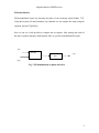
1.2 Analog demodulation in digital domain
AM demodulation
Using square-law approach of envelope detection we can do AM demodulation (Tretter,
129). This approach is a DSP implementation of analog envelope detection. Initially the
signal is squared. Then it is passed through a low pass filter. Finally, the under-root
operation is performed on the signal to get the demodulated output. Thus, the input signal
s=A[1+km(t)]cos ω t is squared to s2=A2[1+km(t)] 2cos2ω t
After passing through the lowpass filter, the output is 0.5A2 [1+km(t)] 2. Square-root
would yield us the desired result but with a DC offset (that can be removed by a simple
high pass filter if required).
4
Implementation of DSP Receiver
x(n)
y(n)
H(ω)
(.)2
√(.)
Lowpass
filter
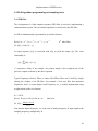
Fig. 1 Square-Law Envelope AM Detector
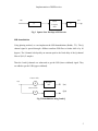
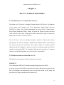
SSB demodulation
Using phasing method, we can implement the SSB demodulation (Rohde, 571). The Q
channel signal is passed through a Hilbert transform FIR filter to further shift it by 90
degrees. The I channel is delayed by an amount equal to the fixed delay of the Q-channel
filter of (N-1)/2 samples.
Then the I and Q channels are subtracted to get the LSB (lower sideband) signal. They
are added to get the USB (upper sideband).
Cos(2 п nf/F)
x(n)
X
Bandpass
filter
I(n)
Hilbert filter
Q(n)
-Sin(2 п nf/F)
X
Fig. 2 Demodulation using I and Q
5
Implementation of DSP Receiver
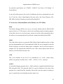
FM demodulation
FM demodulation begins by detecting the phase of the incoming signal (Rohde, 572).
Using the In-phase (I) and Quadrature (Q) channels we can compute the angle using the
equation y[n]=tan-1(Q[n]/I[n])
Here we can use a look-up table to compute the arc tangent. After passing the result of
the above equation through a differentiator filter, we get the demodulated FM signal.
I(n)
Arc tan
Differentiator
filter
y(n)
Q(n)
Fig. 3 FM demodulation by phase detection
6
Implementation of DSP Receiver
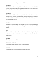
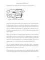
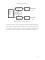
1.3 System Overview
A diagrammatic representation of the DSP receiver in relation to the Personal Computer
(PC) in which it resides is provided below.
CPU System houses the Avr-32
board slotted on the PCB
Analog
Input
sent in
through
the
CPU’s
I/O port
Avr-32 Board with its
TMS320C32 DSP
Command
&
instruction
entry to
Avr-32
Analog
Output
sent
out
Analog
through
Output
the
CPU’s
I/O port
Avr-32 response put on display
Monitor
Screen
Keyboard for control
Fig. 4 System Overview
7
Implementation of DSP Receiver
Chapter 2
The Avr-32 Board and Utilities
2.1 Installation of Avr-32 board & its software
The Dalanco Avr-32 board is a Peripheral Control Interface (PCI) device. The hardware
of the board itself comprises the Texas Instruments Digital Signal Processor
TMS320C32, Xilinx Virtex Field Programmable Gate Array (FPGA), Flash memory,
Direct Digital Synthesizer (DDS), Analog to Digital and Digital to analog converters
(ADC and DAC) and a host of high-speed buffers and numerous ports to connect the
board to the PC itself or to auxiliary devices.
The Avr-32 device driver was installed using the ‘windriver’ folder on the software
package disk. The software package is distributed into different folders each having its
own special contents and read-me file. The ‘Utilities’ folder, for example, provides
applications like the debugger or utilities to install an Assembly program into Flash or
compile its code into the DSP. The ‘Examples’ folder provides Assembly or C programs
on how to run the DSP algorithms or to test the board’s functionalities.
2.2 Hardware features onboard the Avr-32
The Dalanco board comprises the following hardware elements:
TMS320C32
Texas Instruments TMS320C32 floating point digital signal processor (DSP).
It can run at a speed of 60 MHz in two modes; boot loader (When being switched on, the
DSP self-configures and automatically runs from the data stored on the Flash) and
microprocessor (being controlled and run from the PC).
8
Implementation of DSP Receiver
Field Programmable Gate Array (FPGA)
Virtex 2.5V Field Programmable Gate Arrays, Xilinx
It is loaded with the Hex file that configures the input and output from the A/D and D/A
converters and connects the data to the General purpose ATA-IDE, auxiliary digital I/O
or to the local bus on DSP board. It runs the operations using the clock output from the
Direct Digital Synthesizer (coming).
Flash Memory
The Avr-32 has 512 Kbytes of Flash memory which could include initialization code, an
entire application and the data that the application requires. It resides in the
TMS320C32’s memory space at address 900000H.
Analog to Digital Converter (ADC)
It is the 12 bit Analog Devices AD9223. In Virtex test3b mode, it is wired to the upper 12
bits of a 16 bit data word and is clocked by the signal A/D Clock from the FPGA at 2
MSPS (mega-samples per second).
Digital to Analog Converter (DAC)
It is the 12 bit Analog Devices AD9762. In Virtex test3b mode, it is wired to the upper 12
bits of a 16 bit data word and is clocked by the signal D/A Clock from the FPGA.
Direct Digital Synthesizer (DDS)
It is the AD 9850 and provides a high-precision clock output for sampling input and
output with a maximum frequency of 2 MHz.
SRAM
The Static Random Access Memory has 512 Kbytes of memory
Peripheral Control Interface (PCI) Bridge
9
Implementation of DSP Receiver
Its particular specifications are V350EPC, V360EPC Local Bus to PCI Bridge, V3
Semiconductor.
It can work in both master or slave mode. In addition to the above mentioned devices, the
Avr-32 also has a host of Input/Output (I/O) ports such as the General Purpose ATAIDE, DSP serial port, Emulator port and Auxiliary Digital I/O.
2.3 Overview of functionalities of the Dalanco Avr-32 Utilities
D300
The Dalanco debugger D300 is an easy way to become familiar with the TMS320 DSP
aspects of the Avr-32. The feature is used to write and debug simple Assembly programs.
It also allows the user to view the memory contents in real-time. More importantly, this is
the utility to run a program that has been already compiled and loaded into the DSP.
LDDS
This utility allows the user to operate the DDS (Direct Digital Synthesizer) that is a high
precision programmable clock. Upon running the LDDS, the user is prompted to enter the
desired frequency (at which an analog input is sampled in and its processed output is
sampled out). The program then informs the user of the actual frequency that does not
differ by 0.015 Hz from the desired value.
A300
This is the assembler for the Avr-32. Its command line of ‘>A300 {-output mode}
infield’ can generate an outfile with a ‘.COFF’, ‘.ASCII’ or ‘.FLA’ extension.
ASM32
An Assembly language program with a ‘.ASM’ extension is compiled and loaded into the
DSP using this utility. The command ASM 32 is typed in followed by the name of the
program to be compiled and the Assembler either loads it into the system for running or
gives a compile-time error depending on some syntax error.
10
Implementation of DSP Receiver
LOADVIR
This loads the hex file containing the Virtex configuration information into the FPGA.
The Hex file is created by the Xilinx PromptFile Formatter. The default configuration is
the test3b.hex file provided on the installation disk.
LOADCOFF
This utility loads COFF .out files made by the A300 or by the Texas Instruments Linker
into the Avr-32. This utility gives the user the ability to control TMS320 execution. A
complete Loadcoff command follows a special format of preload/postload/output options
for execution of the input file.
LOADF
A program is assembled with the flash flag using the >A300 –f prog1 command. After
erasing any previous code on the flash ‘loadf prog1’ command writes data to the Flash
memory.
LFV
Similar to loadf command, a hex file too can be written to the Flash using this utility. An
additional command called ‘lfvcheck’ ensures that Flash memory has been filled by a
Xilinx hex file.
FLASHE
The utility erases the entire Flash memory.
RDFLASH & WRFLASH
Theses are the reading and writing utilities for the Flash memory
CLRVIR
This program clears the configuration loaded into the Virtex FPGA.
11
Implementation of DSP Receiver
2.4 Issues in DSP Initialization
At the start of the project, the assumption was that the DSP board would be plugged into
the PC and then it will be up and running in a couple of days. However, operating the
hardware through the utilities proved to be a major hassle.
The electronics and systems lab was initially chosen as the venue of the project. The
Pentium-2 PC with the XP Operating system that was proved too slow and consumed a
lot of time in booting up or opening up the Dalanco software package installed on its hard
drive.
The second major difficulty was that the Dalanco user manual was not very useful in
enabling a complete beginner to work on the board. The manual presented the entire
features of the board without coherency. Even some of the names of utility programs on
the manual were different from that on the installation disk. Because of this, there was a
feeling that the Avr-32 software package was too difficult to comprehend.
Due to these difficulties, the vendor was contacted and assistance was frequently sought
on how to operate and use the board. The project venue too was eventually shifted to the
RICE lab with a Windows 98 based Pentium-4.
A summary of the main issues that arose in initiation of the board is given below:
1. Problems with the installation of the device driver in the correct system path caused
some major delays. The XP based PC would not register the Avr-32 device driver in the
system. This problem was solved by changing the PC and installing Windows 98
Operating System.
2. Understanding the work of the debugger was cumbersome. The user manual example
code was difficult to understand and re-implement with changes in the code. Long hours
on the debugger helped get the feel in how to run and work on the D300 debugger.
12
Implementation of DSP Receiver
3. It was also not clear how to program the TMS320C32 DSP with our assembly
programs. The use of the assembler A300 and the process of loading a program into the
TMS320C32 for running became clear after a lot of trial and error. In this regard the help
of the project supervisor Dr. Masud was instrumental in solving the problem and making
the Asm32 up and running. The A300 utility and its complicated usage was avoided by
simply compiling and loading any Assembly program into the DSP by the command
‘>Asm32 myprog’ where myprog is an ‘.ASM’ Assembly program file.
4. Another major problem that was encountered initially was that the Avr-32 would
suddenly ‘freeze’ whilst running the debugger code or some Assembly program and the
whole system would need to be re-booted. Fixing this problem consumed many sessions.
The solution to this problem was to ensure in the Assembly program or the debugger
code that the DSP continued looping in an infinite loop after executing the desired
program.
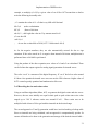
Once these issues were resolved, the process to write programs for the
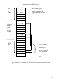
demodulation schemes began.
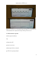
Fig. 5 The actual system setup
13
Implementation of DSP Receiver
Chapter 3
Signal Processing
3.1 Reading Input and Output signaling
The system involves reading in an analog signal and then processing it in the digital
domain. For this purpose, the Dalanco board’s has plenty of provisions. The 12 bit 3
MHz AD converter reads data from Port 14 of the J10 jumper. The converter’s output is
then fed into the Xilinx FPGA which contains the I/O configuration. The data is then sent
to the TMS320C32 DSP. Here our assembled program processes the digital data and
outputs it back to the FPGA. From here on the Digital to Analog converter converts the
data back to analog and outputs it from Port 25.
The control and configuration for the analog input/output of the Avr-32 is done by the
FPGA. The manufacturer provides a Hex file ‘test3b’ to configure it. Additionally it also
provides an Assembly language program ‘addaint.asm’ that performs simple A/D to D/A
pass through - basically, analog signal is read in, converted to digital and from digital
back to analog before being output from Port 25 (a simple pass through).
The ADC and DAC work using the DDS (direct digital synthesizer) which is simply a
precise high speed clock. Once the analog signal is connected to the board, the DDS
samples the signal at the specified frequency. The DDS is run using the ‘Ldds’ command.
Using that program as the basis, the code to process the signals in Assembly language
was further developed. Obviously, it is also possible to change the Xilinx-loaded Hex file
and consequently the configuration of the FPGA. However, for the purpose of simplicity,
the configuration provided by ‘test3b’ was maintained. An additional Hex file called
‘test3’ allowed us to configure the FPGA without involving the DSP. It was a direct pass
through between the ADC and DAC.
14
Implementation of DSP Receiver
Initially, a couple of tests were performed before analog input yielded analog output via
the Avr-32 PCI board. The manufacturer recommended these simple tests to perform
both types of pass-through between the ADC and DAC.
Test 1
;Connect signal generator to port 14 and CRO to port 25. Max Voltage between _+2.5V
;no DSP involved
>Loadvir test3
>Ldds (frequency being kept around 1 MHz) ctrl- c (to exit)
; Observe the cathode ray oscilloscope (CRO)
Test 2
; DSP involved
>Loadvir test3b
>Ldds (frequency being kept around 1 MHz) ctrl- c
>Asm32 addaint
>D300
-g
; DSP run to execute pass through
;Observe the cathode ray oscilloscope (CRO)
15
Implementation of DSP Receiver
3.2 Calibration of the Cathode Ray Oscilloscope
The next major issue involving the input and output of the signal was to calibrate the
ADC and DAC with the Cathode ray oscilloscope (CRO). The DSP works on both
integer and floating point format and initially it was not obvious if the analog signal was
converted to floating points or simply to integers. This led to some programming
problems.
Modifications to ‘addaint.asm’ program were made that would do simple processing of
the input signal. However, none of the initial modifications worked and two complete
sessions of work spent trying to figure out the exact problem.
The modifications included storing in memory a certain number of data samples from the
analog signal and adding or subtracting some value from each of the data sample. The
output of the process in real time was sent to the DAC for output. The data samples
apparently matched to the variations in the analog input. For example, if a sinusoid
analog input with peak to peak value of 1.5 V was applied, the data stored in memory
varied between 1.00346 and 1.00478 with increments of around 0.00003. Addition or
subtraction of values like 0.002 or even 1.00000 to the stored values made no difference
to the analog output.
After much trial and error it was revealed that the problem lay in the debugger D300
command of ‘d.xx’. The symbol ‘xx’ is the memory location where the sample is stored
as a floating point. Thus it should have been ‘dxx’. This also revealed that the analog
signal was being output from the ADC in integer format and it was between the values of
FFFFH and 000FH. The last ‘F’ in the hexadecimal number is reserved for the format of
the FIFO storage configuration of the analog signal.
Hence, a maximum voltage of 2.25 V would get converted to FFFH while a minimum
-2.19 V voltage would generate 000H. Similarly, by trial and error, the zero volts turned
16
Implementation of DSP Receiver
out to be 80BH. A negative number like -1 is represented on the DSP Assembly by
FFFFFFFFH since it follows a 32 bit format.
The whole rage of values generated on the CRO was consequently calibrated with the
hexadecimal numbers generated by the ADC. The next step was to generate an analog
signal of a specific RMS (root mean square) voltage without any input. A square wave
was generated by simply coding two alternating sequences of constant hexadecimal
values that met the desired value (Appendix 1, Square Wave Generation).
3.3 Development of Demodulation Code
The Dalanco Avr-32 board allows the user to implement DSP algorithms in both
Assembly and C. It further allows us to integrate the FPGA and Flash memory into the
development of any communication system.
Because of flexibility and greater control over any communication system software,
Assembly language was used in implementing the algorithms. The Dalanco software
provides examples of simple Assembly programs to read input, do processing on it and
then output it. Using such example programs as the basis, the project-specific code was
developed.
The programs consist of two types of portions. One pertains to manipulating the data and
the other about reading the data from input. The data manipulation comprises simple
load, store, add and multiply instructions to and from registers and RAM memory. The
input/output commands include controlling the pulses to the ADC and DAC and placing
the data in pre-determined memory locations. The FIFO buffers of ADC and DAC have
to be configured to send and receive data. The default FPGA program ‘test3b’ provides
for this.
The code development of the demodulation schemes was divided into several stages. For
each demodulation scheme different code components were needed to do particular tasks.
The tasks are shown below (Rohde, 571):
17
Implementation of DSP Receiver
Amplitude Demodulation
1. Squaring the input
2. Low pass filtering
Frequency Demodulation
1. Generation of I and Q channel streams
2. Dual filtering
3. Division of I and Q streams
4. Arc tangent of two data streams
5. Differentiation of the data stream
Single Side Band Demodulation
1. Generation of I and Q channel streams
2. Dual filtering
3. Addition or subtraction depending on LSB or USB
18
Implementation of DSP Receiver
CPU System houses the Avr-32
that is slotted on the PCB
Analog
Input sent
through
the
CPU’s
I/O port
ADC (Analog to
digital converter)
Xilinx FPGA for
handling input/output
Cathode ray
Oscilloscope
(CRO) for
wave and
signal
display
TMS320C32 DSP
runs the Demodulation
programs
Wave
Generator
DAC (digital to analog
converter)
Command
&
instruction
entry to
Avr-32
Analog
Output
sent
through
the
CPU’s
I/O port
Response from the Avr-32 appears on the
screen
Monitor
Screen
Keyboard for control
Fig. 6 Overall System Schematic
19
Implementation of DSP Receiver
3.4 DSP algorithms programming and sampling issues
3.4.1 FIR filter
The development of a finite impulse response (FIR) filter is critical to implementing a
communications system. The convolution operation is carried out by the FIR filter.
An FIR is mathematically represented by its transfer function:
H(z)=1+a × z -1 + b × z -2 + c × z -3 +…y × z - n
nth order filter
Or h[n]={1,a,b,c,d,…,y}
An input sequence x[n] is convolved with h[n] to yield the output y[n]. The exact
relationship is:
y[n] =
N
∑ h[k ] × x[k − n]
K =0
z-1 represents a delay of one sample. Any output sample is the weighted sum of the
previous n inputs as shown by the above equation.
Typical frequency-selective filters or others like Hilbert filter can be built by simply
altering the weights of an FIR filter. For example, a low pass filter that attenuates
frequencies above a certain digital cutoff frequency ωc, is readily implemented using
weights based on the sinc function.
π= 3.14156
H(z)=1 for |n|<ωc H(z)=0 for |n|> ωc
Or h[n] =
Ideal case
sin(ωc × π × n)
π ×n
Note that the digital frequency, ωc, is the ratio of analog frequency of input signal to the
sampling frequency multiplied by 2π.
20
Implementation of DSP Receiver
We need to convert the non-casual and infinite length h[n] into finite length casual low
pass filter by delaying its output by M samples and taking a rectangular window to
obtain:
h[n] =
sin(ωc × π × (n − M ))
π × (n − M )
0<n<x where n is the desired number of taps
The sequence of h[n] provide the weights of the filter delay coefficients in the H(z)
equation presented above. Similarly, the Hilbert filter is a 90 degree phase shifter (Mitra,
449). Its discrete sample representation is:
h[n] =
1 − cos(π (n − M ))
π × (n − M )
A causal bandpass filter with cutoff frequencies around ωc1 and ωc 2 has the following
coefficients formula (Mitra, 448):
ωc 2 − ωc1
π
for n=0
sin(ωc1× π × (n − M ))
π × (n − M )
sin(ωc 2 × π × (n − M ))
−
π × (n − M )
n>0
h[n] = 1 −
h[n] =
Once an FIR code has been written and programmed, these filter coefficients have to be
scaled to fit the system design and then placed in the memory for the DSP to read.
Writing the Assembly language code to implement an FIR is complicated. Firstly, we
need to have a program that does simple convolution of integers. Secondly, we have to
insert the code that can read and write data in real-time. Due to the limited number of
registers available for specific tasks such as pipelined multiplication or storing A/D data,
the program has to be coded very carefully to optimize register use.
21
Implementation of DSP Receiver
The first task was implemented with the help of FIR code provided in the Texas
Instruments website (Texas Instruments, User Guide). However, the code itself was not
self-explanatory. The other guide on DSP algorithm implementation (Bhaskar, 232) also
provided a program that did not compile on Dalanco Avr-32 Assembler. Thus
modifications had to be made to convolve two sequences using the algorithm concepts
provided in these two references. The resulting program was a static integer convolution
program with a fixed number of inputs (Appendix 1, Static Finite Input FIR Filter).
The second task was to change the filter to convolve integers in real time. As the
equations above would suggest this is a very computation-intensive operation. Analog
signal is digitized and each value is stored at a particular memory location. All values are
then passed through the filter (i.e. convolved) to generate the output values.
The process in real-time involves taking a window of say 1000H data samples from the
input and storing them in a certain memory region. As the first filter calculations are
performed on the data this region quickly fills up. When the 1000H locations are filled
up, a routine called ‘revolver’ that takes the last few data samples then stores them into
the memory region’s start in order to start all over again.
Many changes to the original FIR filter had to be made to be able to perform
computations correctly. In fact, the main problem in dealing with real time sequence of
integers is the calibration of analog output in volts with the data values generated as part
of the Assembly program. Care is needed while multiplying real time data values with
some filter coefficients. We need to ensure that the convolved product of x[n] and h[n]
will be less than 0fffH (4095 decimals) otherwise the output gets clamped and the DAC
stops generating more data samples.
22
Implementation of DSP Receiver
Following is an example of a single 25 Tap FIR memory usage. An additional FIR filter
inside the same program would have similar memory usage except that it would start at
other locations like 16A0H for h[n] and 16F0H for x[n].
h[n]
starts
at
100H
h[0]
100H
h[1]
101H
h[2]
102H
Pre-programmed
25 tap
coefficients
written to 25
locations
between 100H
and 118H.
These locations
are tapped every
time an output is
to be calculated
.
.
h[24] 118H
.
All these
locations
are
initialized
to zero as
dummy
inputs
x[-24] 137H
.
x[-21] 13AH
.
x[-3] 14DH
x[-2] 14EH
x[-1] 14FH
Input x[n]
fills in
this
direction
for
1000H
locations
x[0]
150H
x[1]
151H
x[2]
152H
x[3]
153H
25 input
memory
locations
used in
producing
every
output.
This time
it is y[3].
Example y[3] for x[3]
y[3] = x[3].h[0] +
x[2].h[1] + x[1].h[2] +
x[0].h[3] + x[-1].h[4]
+…x[-21].h[24]
The convolution
equation:
N
y[n] = ∑h[k]×x[k −n]
K=0
.
.
x[4432]
1150H
Maximum address for
input storage
.
Fig. 7 DSP RAM Memory
23
Implementation of DSP Receiver
h[n]
starts
at
100H
h[0]
100H
h[1]
101H
h[2]
102H
.
Once 1000H memory
locations are filled up its
time to re-start from the
original locations since the
DSP memory is limited.
.
h[24] 118H
.
Initialized
dummy
inputs
locations
are now
filled up
x[-24] 137H
.
.
.
x[-3] 14DH
x[-2] 14EH
x[-1] 14FH
Input x[n]
fills in
this
direction
x[0]
150H
x[1]
151H
.
x[4407] 1137H
.
x[4431] 114FH
x[4432] 1150H
.
Last 25 memory
locations
containing the
latest input values
are revolved back
to the initialized
locations that
originally held
zeros
Fig. 8 ‘Revolver’ re-initializes the convolution from original memory locations
24
Implementation of DSP Receiver
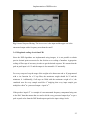
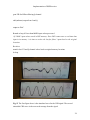
Fig. 9 Actual lowpass filtering. The lower wave is the input and the upper one is the
attenuated output with a frequency more than the cutoff
3.4.2 Magnitude scaling of real-time FIR
Since the DSP algorithms are implemented using integers, it is not possible to obtain
precise decimal point accuracies for the division or re-scaling of numbers. Appropriate
scaling of filter taps of necessary in order to get the desired response. We assume that the
peak to peak input is 4.0 V and the output is also around 4.0 V maximally.
For every n taps we keep the range of the weights to be between n and -n. If programmed
with a sinc function for a 25 tap filter, the maximum weight should be 25 and the
minimum -8. Additionally, if all taps are filled with the maximum weight of ‘n’, the
combined sum for every sample would be n2 implying that every input sample gets
multiplies with n2 or ‘processed output = input* n2’.
If the product ‘input* n2’ is a sample of a non-attenuated frequency component being sent
to the DAC then that means that we need to divide every processed output by n2 to get a
peak to peak value from the DSP board output equal to the input voltage levels.
25
Implementation of DSP Receiver
But we also need to scale down this value to between the desired levels of 0cffH (+2.0 V)
and 100H (-2.0 V) to get a total of 4.0 V peak to peak. For our n tap filter, we need to
right shift every processed sample prior to being sent to the DAC that would wholly
divide n2.
# Right shifts, k = log (n2)/log(2)
Since every right rotation is a division by two, the number n2 becomes one if divided by
k. This mechanism ensures that we are able to get the desired response within acceptable
peak to peak voltage levels of around 4 V if un-attenuated. The above formula is usable
just for a one-filter system. For specific demodulation schemes with multiple filters and
the I and Q channels, there is a larger value of ‘k’.
AM demodulation scheme
K = log(2* n2)/log(2)
SSB demodulation scheme
K = log( c × 2 × n2)/log(2)
c = sinusoidal computation steps for I or Q stream
FM demodulation scheme
In case of the FM, the tasks of division of I and Q channels and subsequent processing of
arc-tangent and differentiation were not completed by the end of the project and hence a
formula cannot be given.
3.4.3 ADC sampling rates and program speed
26
Implementation of DSP Receiver
The number of clock cycles performed in order to correctly produce one output sample
for every input sample is the requisite of selecting the maximum sampling rate for the
receiver system. Since high digital frequencies (digital frequency = input frequency /
sampling rate × 2 × π) imply less quantization noise and are desirable hence we would
like to keep the sampling rates to as close to 2 MHz (maximum sampling rate) as
possible. Furthermore, since keeping in view that the message or broadcast riding on the
carrier waves would have a range of 20 Hz to 5 KHz, we would also like to sample
sufficiently fast so that the original message is recovered from the carrier.
We have two programs; one for AM demodulation and the other one for the SSB. Since
clock cycles per instruction were not provided in the Texas Instruments manual, the
number of cycles per instruction had to be estimated.
Clock cycles per instruction
1) Br
4
branch
2) Ash
1
arithemetic shift
3) ldi,sti
1
load, store
4) mul,addi, subi
1
multiply, add, subtract
5) mul3, addi3, subi3
2
multiply, add, subtract
6) FIR Filter
N+11
N is number of taps (Texas Instruments)
By counting the lines of code and multiplying each line with its corresponding clock
cycles we derive:
AM cycles:
93+ n
SSB cycles:
133+ 2n
27
Implementation of DSP Receiver
FM cycles (an estimated value is derived since this demodulation program was not
completed):
200 +3n
Since each clock cycle is at 60 MHz , it means that between every data sample, the DSP
spends (200+3n)/60M seconds for the most computation-intensive scheme like the FM.
Hence the maximum clock sample is 6000000/(200+3n) or 220 KHz for FM with 25 taps.
The 220 KHz rate easily satisfies the Nyquist criterion for the human voice up to 5 KHz.
Obviously high quality and minimal quantized error are not the objectives for this radio
system.
If we exceed this sampling rate and we will be doing decimation of output frequency. For
each input sample, its processed output sample appears after several more input samples
have already appeared. The overall frequency of the output signal is thus less than that of
the input signal.
3.4.4 I/Q Channel Generation using Digital Oscillator
We need two sequences of sinusoidal waves out of phase by 90 degrees that are
multiplied by the incoming data sequence to generate the I and Q channels. Although the
theoretical procedure for I and Q generation was provided in the references (Rohde, 571)
and (Mitra, 407) but their actual implementation in integer format proved to be
complicated. The problem was compounded by the fact that there is no straight forward
way to divide two integers or floating point numbers. Hence ways and means had to be
found to overcome the problem of multiplying an integer with a fraction.
Mathematically, the In-phase (I) and Quadrature (Q) channels can be represented as
(Rohde, 571):
Q[n] = x[n] × - sin (2πnω)
I[n] = x[n] × cos (2πnω)
28
Implementation of DSP Receiver
ω=digital frequency = f/F × 2π where f is incoming signal frequency and F is the
sampling rate
Initially, simultaneous sine and cosine waves were generated. The next step was to
multiply in real time the incoming data sequence and pass it through lowpass filters to be
able to generate the two sequences I and Q.
There were two approaches to this. One was to write a code that computed sinusoidal
hexadecimal values that would be converted to analog equivalent. The other was to read
into the DSP a sinusoidal signal and store its contents in memory as part of a lookup
table. Then using this lookup table, the I and Q channels could be generated. Both the
approaches were tried but it turned out that first method was accurate and easier, though
more computation-intensive than the lookup table’s method.
The first approach was implemented by implementing a digital sine-cosine generator
(Mitra, 405). Mathematically, a sine-cosine generator is given by:
s1[n] = a × sin(nθ)
s1[0] set to an initial value of 64H
s2[n] = b × cos(nθ)
s2[0] set to an initial value of 0H
s1[n+1]= cos θ × s1[n] + (cos θ +1) × s2[n]
s2[n+1]= (cos θ -1) × s1[n] + cos θ × s2[n]
29
Implementation of DSP Receiver
A diagrammatic representation of the sine-cosine generator is provided below.
S1
× cos θ
Add
× cos θ
S2
Sub
Add
Fig. 10 Flowchart of the digital oscillator
A digital sine-cosine generator initially involves taking the cosine θ value that represents
the digital frequency of the wave to be produced. Using the above iterative algorithm, an
Assembly program on DSP was written to produce sine and cosine values. However, this
was not a straightforward implementation. The algorithm had to implement division of
two integers to get the product of cos θ × (s1+s2). It also had to have provisions to divide
negative numbers.
Initially, the rotate right (‘ror’) Assembly language instruction was used in performing
division. However, this was a very inefficient way of rotating right since to rotate ten or
twelve times, one clock cycle was used for every rotation. Fortunately just in the final
days as the code was being optimized so as to minimize the programs’ clock cycles, an
alternative to the ‘ror’ was found in form of the ‘ash’ instruction (Bhaskar, 203)
The ‘ash’ instruction arithmetically performs a shift right or left in a sign-extended
manner depending on the value stored in the register. Thus through such an instruction,
the program can save a dozen or so clock cycles!
The division feature was developed using the ‘ash Rx’ command that shifted the contents
of a processor register right by one bit catering for the sign of the value stored in Rx. For
30
Implementation of DSP Receiver
example, to multiply (s1+s2) by a given value of cos θ like 0.875 meant that we had to
write the following Assembly code:
; r3 contains the value of s1 +s2 that is say 64H or100 decimal
ldi r3,r4
;make a substitution
ldi 3,r2
;factor of division
ash r2,r3 ; shift right the value in r3 by amount stored in r2
;r3 now has 8H
subi r3,r4
;
r4 now has a value 88d or 58H (0.875 * 100 decimal =88 d)
As for the negative numbers, they are also automatically catered for due to sign
extension. If the value stored in r2 is negative then instead of division, multiplication is
performed since a left shift is performed.
Using the product of the above equation, new values of s1 and s2 are calculated. These
can be fed into the output register for analog signal generation of sinusoid waves.
The value ‘cos θ’ is a measure of the digital frequency. If ‘cos θ’ had a low value around
0.5 then a less quantized sinusoid wave was seen on the CRO whereas a higher value of
0.875 created a greatly quantized and random noise-like wave.
3.4.5 Rescaling the sine and cosine values
Using an oscillator algorithm (Mitra, 407) we generate the digital cosine and sine waves.
However, the two were initially not equal in their peak to peak values since sine value
ranged up to 3.84 V whereas cosine was around 85 mV.
Thus cosine was to be
multiplied with a factor of 46 to get both the sinusoids in the desired range.
The second approach of I and Q generation would have involved making a lookup table.
Since no sinusoids are being calculated, such an approach is computationally quicker. In
essence all that has to be done is the generation and storage of the desired sinusoid table –
31
Implementation of DSP Receiver
a goal that can be performed by an initializing program that is also tasked with burning
the tap coefficients into the memory. Then, in theory at least, once the actual receiver
program runs, it will merely pick all those stored values from memory locations and
produce digital oscillation for generating I and Q channels.
However, contrary to expectation this task proved to be very challenging and was
eventually dropped in favor of the first approach. Maintaining the 90 degree phase
difference between sine and cosine waves was a very complex task whilst the digital
frequency was varying.
The digital frequency is the scaled ratio of input frequency (which can obviously change)
and sampling rate (which is more or less fixed). The sinusoid lookup table generated by
the initializing program could not be adaptively sampled to generate the desired
frequency. Suppose that for a ω (digital frequency) of 0.9 rad/sec the initializing program
created 1000 digital oscillation samples and burned them onto the memory. If ω changed
to say 0.4 rad/sec (which it would as we would change the input frequency) then this
means that we need to pick every (0.9/0.4)=2.25 alternate samples from the table.
Clearly, it would be impossible to create an accurate sine or cosine wave using a table
with a limited number of entries.
3.4.6 Integration of I/Q channels and dual filters
Multiplying the sinusoids with the input involved using an instruction like ‘mul’ that
could multiply the values stored in two registers - one having a sinusoid sequence value
and the other having the input value from ADC. However, this did not produce the
correct output without some important modifications being made.
The original output was a very random signal with a peak to peak often exceeding 4.5 V.
Quite often a couple of seconds after the I/Q channel generator started running, the DAC
of the DSP would become flat-lined. This was an indication that the output was actually
much in excess of the maximum values (peak to peak of 4.48 V) that the DAC could
send.
32
Implementation of DSP Receiver
This problem was resolved by scaling down the product stored by the internal sinusoidal
and input multiplication. For example, if an input processed after the A/D conversion
with a value of 0BFFH was multiplied with a sinusoidal value of 0A00H then the output
is 77f600H - a value simply too large for DAC (that can process a maximum of 0FFFH).
Thus by arithmetically right shifting the value 77F600H by 12 times we obtain 77FH, a
value feasible for the DAC.
The output on the CRO for an internal sinusoid multiplying with an external sinusoid was
a rapidly modulating signal. If an input signal of 2 Hz was provided, then we could
observe on the CRO that a sinusoid wave was rising and falling at a rate of 2 peaks per
second. At one moment its peak to peak was say 3.1 V while the next moment around 3.7
V and so on. Finally within a second it would come back to the original value of 3.1 V.
By now, either the I/ Q channels or the filters could be run by a single program but not
both. The challenge was to place both the channels and the filters within the same
program. This was problematic because the use of registers had to be optimized. Some
registers also did not work correctly (coming). However by modularizing the FIR filter
code, a few registers were saved in order to producing the second channel.
When it was being developed, the program was tested as every important line or a block
of code was added. The actual output was matched with the desired output to find out any
problems. The register r9, as mentioned earlier, was not working at all (could not be used
for adding, multiplying or loading) in the second filter. Despite a lot of effort being made
to understand why this was so, no solution was found. Consequently, r9 was not used in
the second filter code.
Once the multiple filters and the digital oscillator were programmed inside a single
master-program, a series of tests were performed to ascertain that they were functioning
correctly. These tests are discussed under the subsequent title ‘Testing Phase’.
33
Implementation of DSP Receiver
3.4.7 Initializing program
The running of FIR filters requires burning tap coefficient weights in the memory. Since
we mainly use two 25 Tap filters it was very cumbersome to manually enter the weight
values each time a demodulating or filtering program was run. Hence, an initializing
program called the ‘tapburner.asm’ was written that would be run before any filtering or
demodulating program was started.
The task of the ‘tapburner.asm’ would simply be to place the values of the weight
coefficients in the memory locations from which the FIR filters would read their taps.
Hence if the coefficients for a filter were to reside at locations 200 H to 219H then the
initializing program would store pre-determined values (as set by the programmer) onto
those locations. Such initialization substantially sped up the work of fine-tuning the
operations of the demodulation programs.
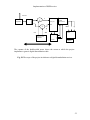
3.4.8 System modularization
The generic DSP radio receiver has four primary modules that generate I and Q channels
and apply filters; -sine multiplier, cosine multiplier, FIR1 (first filter) and FIR2 (second
filter).
The digital oscillator generates −sine and cosine waves that are multiplied with the
incoming input sequence. The filters FIR1 and FIR 2 are two 25 tap FIR filters that can
be programmed to do lowpass, bandpass or Hilbert filtering.
34
Implementation of DSP Receiver
-sin (2πnω)
Deformatted
input
from
ADC
FIR 1
I[n]
Digital
Oscillator
cos(2πnω)
FIR 2
Q[n]
Fig. 11 The DSP receiver system as modules
In case that a module is de-activated (bypassed essentially), the data stream from the
ADC continues to pass through it without being affected by the module itself. Hence if
the ‘cos(2π ω)’ and ‘FIR1’ modules are non-active, the input signal will continue to be
processed by ‘FIR2’ and ‘-sin (2πnω)’ as if ‘cos(2πnω)’ and ‘FIR1’ were not present.
35
Implementation of DSP Receiver
Chapter 4
Demodulation Algorithms
Following are the algorithms of the various programs that have been written to
demodulate the input signals. They are a crude approximation to the actual Assembly
code. The actual code is provided in Appendix A.
4.1 AM Demodulation Algorithm
initialize registers & mailboxes
loop:
read input from ADC
square the input
goto FIR1 for lowpass filtering
output the output of FIR 1 to DAC
Branch to loop if fewer than1000H input values processed
//if 1000H input values stored in DSP memory. Since DSP cannot store a real-time data
input in its memory it is time to revolve the last few filters’ inputs back to the original
locations.
Revolver:
Transfer the last 25 I and Q channel values back to original memory locations
br loop
36
Implementation of DSP Receiver
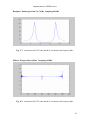
Fig 12. The first CRO wave is the simulated squared AM signal. The second CRO wave
is the demodulated DC component after lowpass filtering of the same wave.
4.2 SSB Demodulation Algorithm
initialize registers & mailboxes
loop:
read input from ADC
generate sine and cosine
multiply input with the two sinusoids
goto FIR1 for low-passing I channel
37
Implementation of DSP Receiver
goto FIR for Hilbert-filtering Q channel
add (subtract) output from I and Q
output to DAC
Branch to loop if fewer than1000H input values processed
//if 1000H input values stored in DSP memory. Since DSP cannot store a real-time data
input in its memory it is time to revolve the last few filters’ inputs back to the original
locations.
Revolver:
transfer last 25 I and Q channel values back to original memory locations
br loop
Fig. 13 The first figure above is the simulated wave for the USB signal. The second
sinusoidal CRO wave is the recovered message from the signal.
38
Implementation of DSP Receiver
Fig. 14 The above CRO waves show the effect of a Hilbert filter. Notice the 900 phase
difference between the input and the output.
4.3 FM Demodulation Algorithm
(Not fully developed)
initialize registers & mailboxes
loop:
read input from ADC
generate sine and cosine
multiply input with the two sinusoids
goto FIR1 for low-passing I channel
goto FIR for Hilbert-filtering Q channel
39
Implementation of DSP Receiver
divide I channel with Q channel
use lookup table to find the arc tangent of the value (I/Q)
output to DAC
Branch to loop if fewer than1000H input values processed
//if 1000H input values stored in DSP memory. Since DSP cannot store a real-time data
input in its memory it is time to revolve the last few filters’ inputs back to the original
locations.
Revolver:
transfer last 25 I and Q channel values back to original memory locations
br loop
40
Implementation of DSP Receiver
Chapter 5
Testing Phase
The overall system testing phase is the process by which the correctness of the system
software is verified. Since this project is oriented more towards the DSP side, emphasis
was placed on developing the Assembly programs for the demodulation schemes. It was
not possible to obtain the radio transmitters that would be processed by the DSP radio
receiver and hence verification if the software was working correctly had to be done by
alternative methods.
The testing approach that was adopted can be described as modular or as Bottom-Up
approach if a software engineering term is to be borrowed. The programs would be
verified and corrected module by module as the scope of the testing expanded. Once each
module was functioning correctly, their working as parts of an integrated system was
checked. Since each module was functioning properly independently, the testing phase
was about incorporating them in an integrated program and verifying correct operation.
The development of real time filters and the In-phase and Quadrature channels has been
described earlier. These modules were embedded in three separate programs for AM,
SSB and FM demodulation. The desired output was generated by MATLAB (see
Appendix B) and was compared with the actual output. If there was a 100 percent match
then the demodulation programs were working fine.
The testing plan for each demodulation scheme is described below.
5.1 Single filter operations
FIR1 enabled; all other modules disabled
41
Implementation of DSP Receiver
Following test is repeated for the second filter by switching the tap values and same
results obtained
Input: Sinusoid with frequency 1000 Hz
FIR 1 Taps: 0,0,0,0,0,0,0,0,0,0,1,0,0,0,0,0,0,0,0,0,0,0 (25 taps)
FIR 2 Taps: 0,0,0,0,0,0,0,0,0,0,0,0,0,0,0,0,0,0,0,0,0,0 (25 taps)
I/Q channels Active: No
Desired Output: A delayed version of input with same peak to peak voltage
Test Output: As desired
5.2 Digital Oscillator operation
FIR1, FIR2 disabled; I and Q modules enabled
Following test is repeated for the sine by switching the output and same results obtained
as below
Input: None needed
FIR 1 Taps: None needed
FIR 2 Taps: None needed
I/Q channels Active: Yes
Desired Output: A sinusoid wave with an output peak to peak of around 4 V generated of
a cosine.
42
Implementation of DSP Receiver
Test Output: As desired with the peak to peak around 3.84 V for both sinusoids
5.3 I channel operation
FIR1, digital cosine enabled; all other modules disabled
Following test is repeated for the Q channel by swapping the tap values between FIR 1
and FIR 2. Same results are obtained as below.
Input: Sinusoid with frequency 1000 Hz
FIR 1 Taps: 1,0,0,0,0,0,0,0,0,0,0,0,0,0,0,0,0,0,0,0,0,0 (25 taps)
FIR 2 Taps: 0,0,0,0,0,0,0,0,0,0,0,0,0,0,0,0,0,0,0,0,0,0 (25 taps)
I/Q channels Active: Yes
Desired Output: Depending on input frequency, an oscillating sinusoid generated with the
frequency of oscillation equal to input frequency. The fluctuating value of peak to peak
voltage of the output depends on the amplitude of the input
Test Output: As desired
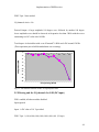
5.4 Operation of the filter for AM demodulation
All other modules enabled
Input: A 1.0 V peak to peak sinusoid provided
FIR 1 Taps: -3
13
8
-5
-5
3 -1 -4 -5
-5
-4
-1
3
8
13
18
22
24
25
24
22
18
-5 -5 -3 (25 taps)
43
Implementation of DSP Receiver
FIR 2 Taps: None needed
I/Q channels Active: No
Desired Output: A large amplitude 180 degree wave followed by another 180 degree
lower amplitude wave should be observed at frequencies less than 5 KHz with the waves
attenuating to a DC value after 10 KHz
Test Output: As desired but with a cut off around 7.0 KHz and a DC around 15 KHz
(This experiment proved AM demodulation was occurring)
0
-2
0
1
3
5
6
7
10
12
15
20log10|H(ω)| dB
-4
-6
-8
-10
-12
-14
-16
-18
Frequency (KHz)
Fig. 15 The transfer function of the 25 tap lowpass filter
5.5 Filtering and the I/Q channels for LSB (DC input)
FIR 1 enabled; all other modules disabled
Input squared
Input: A DC value of 1.0 V provided
FIR 1 Taps: 1,0,0,0,0,0,0,0,0,0,0,0,0,0,0,0,0,0,0,0,0,0 (25 taps)
44
Implementation of DSP Receiver
FIR 2 Taps: 1,0,0,0,0,0,0,0,0,0,0,0,0,0,0,0,0,0,0,0,0,0 (25 taps)
I/Q channels Active: Yes
Desired Output: The sum of I and Q channels should be a 1.86 V peak to peak sinusoid
(This is the test for LSB where I and Q channels are added)
Test Output: As desired with a peak to peak sinusoid of 1.84 V!
(This experiment proved that both the filters alongside the digital oscillators were
working as part of an integrated system)
5.6 Filtering and the I/Q channels for LSB (AC input)
FIR 1 enabled; all other modules disabled
Input squared
Input: A sinusoid with a 1.0 V peak to peak sinusoid provided
FIR 1 Taps: 1,0,0,0,0,0,0,0,0,0,0,0,0,0,0,0,0,0,0,0,0,0 (25 taps)
FIR 2 Taps: 1,0,0,0,0,0,0,0,0,0,0,0,0,0,0,0,0,0,0,0,0,0 (25 taps)
I/Q channels Active: Yes
Desired Output: The sum of I and Q channels should be an oscillating sinusoid (This is
another test for LSB where I and Q channels are added)
Test Output: As desired with a peak to peak sinusoid of 1.4 V
(This experiment proved that both the filters alongside the digital oscillators were
working as part of an integrated system)
45
Implementation of DSP Receiver
5.7 Operation of the filters and the I/Q channels for Band Pass filtering
FIR 1 enabled; all other modules disabled
Input squared
Input: A sinusoid with a 1.0 V peak to peak sinusoid provided
FIR 1 Taps:
-1 -11
-1
-9
1
10
1 12 -1 -12 1
-1 -10
1
10
-1 -10
1
11
-1 -11
1
11
(25 taps)
FIR 2 Taps: None needed
I/Q channels Active: No
Desired Output: The a sinusoidal wave should be generated between 4 to 7 KHz
Test Output: Not As desired but with a band-pass range of 16.0 to 20 KHz. If the number
of taps is increased substantially only then will the desired response will be achieved.
5.8 Operation of the filters and the I/Q channels for Hilbert filtering
FIR 1 enabled; all other modules disabled
Input squared
Input: A sinusoid with a 1.0 V peak to peak sinusoid provided
FIR 1 Taps:
3
0
2
0
-1
0
-1
0
-2
0
-2
1
0
1
0
1 (25 taps)
0
-4
0
-8
0
25
0
5
0
46
Implementation of DSP Receiver
FIR 2 Taps: None needed
I/Q channels Active: No
Desired Output: The a sinusoidal wave should be out of phase with the input by 90
degrees
Test Output: As desired
47
Implementation of DSP Receiver
Chapter 6
Filter Specifications And Weight Calculations Using
MATLAB
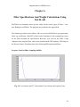
MATLAB was frequently used to get the values for the various types of filters – Lowpass, Band-pass and Hilbert. The programs are provided in the Appendix B.
The formulas provided in texts (Mitra, 448) were used in MATLAB to get approximate
filters’ tap coefficients. If the FFTs (Fast Fourier Transforms) of the computed tap values
for the filters matched the specifications then they were used on the DSPs. Using
‘tapburner.asm’ program, these values were encoded on the DSP memory. Following are
the Discrete Fourier Transform plots of the following FIR-implemented filters.
Lowpass: Cutoff at 5Khz Sampling=40 KHz
Fig. 16 Y axis denotes the FFT value and the X axis denotes the frequency bins;
48
Implementation of DSP Receiver
Bandpass: Band region from 5 to 7 KHz Sampling=40 KHz
Fig. 17 Y axis denotes the FFT value and the X axis denotes the frequency bins;
Hilbert: 90 degree Phase shifter Sampling=40 KHz
Fig. 18 Y axis denotes the FFT value and the X axis denotes the frequency bins;
49
Implementation of DSP Receiver
Chapter 7
Project Expansion and Assessment
7.1 Integration of analog electronic hardware with the DSP Board
An addition to the project (though not part of the stated objectives) would involve
amalgamating the DSP part and the analog electronics to capture a signal and to produce
the voice output.
The typical frequencies for AM radio stations range between 100 KHz to 2 MHz and are
far high for the Avr-32 ADC. Hence a signal captured by the system’s antenna would
have to be translated to a frequency of around 20 KHz . Such a sampling value is chosen
because of the fundamental limits imposed by the inter-sampling computational rate of
around 220 KHz (see ‘ADC sampling rates & program speed’ above). Similarly, the
frequency ranges of the FM and the SSB (88 MHz to 110 MHz and 10 MHz to 30 MHz
respectively) are also far too high for the ADC even if it were operating at its maximum
limit of 2 MHz. The use of a frequency down-converter is inevitable.
The analog components include the following items:
1. Antenna
2. Pre-amplifier and amplifier stages
3. Earphones to listen to the output
4. Tunable frequency translator or down-converter
Additionally the following electronic circuit was built and used for testing the analog
signal for amplitude demodulation (Cappels, September 2002). It however suffered from
the problem of being simply too fast for the DSP even when its crystal was changed from
4 MHz to 455 KHz.
50
Implementation of DSP Receiver
Fig. 19 Amplitude Modulated Oscillator
7.2 The generic DSP radio as a digital receiver
The testing phase of the project demonstrated that demodulation schemes for both AM
and SSB (both USB and LSB) were completed with work for the FM partially done. With
some additional time the FM demodulation scheme would have been completed too.
Thus two out of three goals as stated in the ‘Project Objectives’ earlier have been met.
The goal and direction of any future project based on the current project could be to
develop a complete communication system that can also be programmed as a digital
receiver. The program written for the SSB can be modified to become a generic digital
communications receiver in DSP. It has a digital oscillator and two initial filters that yield
I and Q channels for demodulation. In fact our DSP radio receiver is not very different
from the following digital receiver (Digital Receivers Bring DSP to Radio Frequencies).
51
Implementation of DSP Receiver
Antenna
RF
Amplifier
Decimating
I
×
ADC
Low pass
Detector
(DSP
Processor)
filter
×
Cos
Real
I
Q
Q
DAC
-Sin
Output
Digital Local
Oscillator
format
Speaker
The expanse of the double-sided arrow shows the extent to which the project
implements a generic digital demodulation radio
Fig. 20 The scope of the project in relation to a digital demodulation receiver
52
Implementation of DSP Receiver
Appendix 1: DSP programs in Assembly
1. Square Wave Generation (Ad3.asm)
The following program generates a square wave with pre-determined maximum voltage
and frequency. No input is provided.
; addaint.asm
Reset
.word
start
; location 0
.aorg
2
.word
Int1handler
.aorg 40H
CTRL
.word
808000H
STRB0_CNTRL .word
0F1018H ; 0 ws
IOSTRB_CNTRL
.word
TIME
018H
; 7 ws
.word 3H
ADDA
.word 220000H ; 810000H
ADDAFIFOSTAT
.word 220001H ; 810000H
MEMLOC
.word
MASK
.word 2
POS
.word 1000H
POS2
.word 1020H
start: LDP
100H
; 2 for INT1
0H
LDI
200H,SP
; SET STACK POINTER;
LDI
5800H,ST
; CACHE DISABLE
LDI
@CTRL,AR0
LDI
@STRB0_CNTRL,R0
STI
R0,*+AR0(64H)
LDI
@IOSTRB_CNTRL,R0
STI
R0,*+AR0(60H)
LDI
@ADDA,AR2
LDI
@ADDAFIFOSTAT,AR3
LDI
@MEMLOC,AR4
; SET WAIT STATES
; SET WAIT STATES
53
Implementation of DSP Receiver
LDI
@POS, AR5
LDI @POS2,AR6
LDI 30,BK
;unmask interrupts
Main:
LDI
@MASK,IE
OR
2000h,ST
"TMS320C32"
; global interrupt enable.
br @Main
Int1handler:
aa:
ldi
0,r0
sti
r0, *ar3
ldi
*ar2,r0
; acknowledge interrupt
;% do all signal processing here to value in r0
ldi 7fffh,r1
xx: ldi 0000ffffh,r0
sti
r0, *ar3
sti r0, *ar2
sti
r0,*ar5++(1)%
subi 1,r1
bnz xx
ldi 1900h,r1
yy: ldi 0000fffh,r0
mpyi -1,r0
mpyi 10H,r0
OR 0000000FH,r0
sti
r0, *ar3
sti
r0, *ar2
sti
r0,*ar5++(1)%
54
Implementation of DSP Receiver
subi 1,r1
bnz yy
br aa
sti
r1,*ar6++(1)%
reti
.end
2. Static Finite Input FIR Filter (f3.asm)
The following program does not do real-time signal processing. Rather it picks some
stored values from memory (h[n] at 350H and x[n] at 360H) and performs convolution on
them and stores the results to 370H. The user needs to enter the tap and inputs from the
locations specified.
Reset
.word start
; location 0
temp1
.word 350H ;x
temp2
.word 360H
temp3
.word 370H
;h
;y
start:
ldi @temp1,ar1
;x
ldi @temp3,ar2
;y
ldi 0aH,r5 ; value of r5 is the number of inputs .Infinite in case of realtime signal
ldi 0,r6
loop: ; start loop to convolve data
ldi @temp1,ar1
;x .Store every new real time signal point here
; addi ar1++(1)%
addi r6,ar1
; keep moving forward
addi 1,r6
; necessary in real time too
ldi @temp2,ar0
;h
ldi 0,r0
55
Implementation of DSP Receiver
LDI 3,RC
; load n-2 where n is the number of taps including the first non-delay one too
LDI 5,BK
;load n which is the total number of delay taps+1 i.e 4+1
br FIR
ret:
;addi 3,ar1 ;increment x[i] i.e read further data
subi 1,r5
; decrement and see if there's end of data line
bnz loop
; in real time signals keep looπng and no subi 1,r5
jj:
br jj
FIR:
mpyi3 *ar0++(1),*ar1--(1),r0
ldi 0,r2
RPTS RC
MPYI3 *AR0++(1),*AR1--(1),R0
|| ADDi3 R0,R2,R2
ADDi3 R0,R2,R0
STi R0,*AR2++(1)
br ret
.end
3. Real Time FIR Filter (rtfir10.asm)
This performs filtering based on the FIR algorithm in real-time. Stored values start from
100H for h[n]. Alternatively he can run the program ‘tapburner.asm’ to place predetermined at the specified locations. Input start getting placed from 150H for x[n]. After
the ‘revolver’ runs, the inputs get placed from location (150 – N) Hex onwards. (N is the
number of taps in hexadecimal).
Reset
.word
start
; location 0
.aorg 2
.word
Int1handler
;f3.asm
.aorg 40H
CTRL
.word
808000H
56
Implementation of DSP Receiver
STRB0_CNTRL .word
0F1018H ; 0 ws
IOSTRB_CNTRL
.word
TIME
018H
; 7 ws
.word 3H
ADDA
.word 220000H ; 810000H
ADDAFIFOSTAT
.word 220001H ; 810000H
MEMLOC
.word
MASK
.word 2
; 2 for INT1
temp1
.word 150H ;x
temp2
.word 100H
temp3
.word 400H
temp4
100H
;h
;y
.word 14fH ;temp4=temp1-1
start: LDP
0H
LDI
200H,SP
; SET STACK POINTER;
LDI
5800H,ST
; CACHE DISABLE
LDI
@CTRL,AR6
LDI
@STRB0_CNTRL, R0
STI
R0,*+AR6(64H)
LDI
@IOSTRB_CNTRL, R0
STI
R0,*+AR6(60H)
LDI
@ADDA,AR2
LDI
@ADDAFIFOSTAT, AR3
Main:
LDI
@MASK,IE
OR
2000h,ST
; SET WAIT STATES
; SET WAIT STATES
; global interrupt enable.
br @Main
Int1handler:
ldi @temp1,ar1
;x(0)
ldi @temp4,ar7
;x(0)
ldi @temp3,ar5
LPF:
ldi 1000H,r5 ; value of r5 is the number of inputs
ldi 1,r4 ;r4 is increments to x[n+r4]
57
Implementation of DSP Receiver
loop: ; start loop to convolve data
LDI 23,RC
; load n-2 where n is the number of taps including the first non-delay one too
LDI 25,BK
;load n which is the total number of delay taps+1
ldi
0,r0
; acknowledge interrupt
sti
r0, *ar3
ldi
*ar2,r0
ldi r0,r1
AND 00000fff0h,r1
ror r1
ror r1
ror r1
ror r1
subi 80bH,r1 ;r0 stripped of all formalities
sti r1,*ar1
ldi @temp2,ar0
;h
br FIR
ret:
ldi @temp1,ar1
;x
addi r4,ar1
addi 1,r4
subi 1,r5
; decrement and see if there's end of input seq
bnz loop
br revolver
revolverback :
br lpf
jj:
br jj
FIR:
mpyi3 *ar0++(1),*ar1--(1),r1
ldi 0,r2
RPTS RC
58
Implementation of DSP Receiver
MPYI3 *AR0++(1),*AR1--(1),r1
|| ADDi3 r1,R2,R2
ADDi3 r1,R2,r1
ldi r1,r9
ror r9
ror r9
ror r9
ror r9
ror r9
ror r9
ror r9
ror r9
ror r9
ror r9
AND 0000FFFFH,r9
addi 80bH,r9
mpyi 10h,r9
ldi r9,r0
sti r0, *ar1
;store this in order to re-process the signal
sti r0, *ar2
br ret
; RETSU
revolver:
LDI
@temp4,ar7
LDI
@temp1,ar1
LDI
0,r4
ldi 0fffH,r8
; n is sample inputs
addi r8,ar1
ldi 24,r1
;no of taps -1
alpha:
ldi *ar1--(1),r6
sti r6,*ar7--(1)
subi 1,r1
bnz alpha
ldi @temp1,ar1
;x(0)
59
Implementation of DSP Receiver
LDI
0,r4
br lpf
.end
4. Digital Oscillator (finalIqi.asm)
This program internally generates -sine and cosine waves but only one of them can be
output at a time. Externally it outputs the product of the input signal and one of the
sinusoids.
; addaint.asm
Reset
.word
start
; location 0
.aorg
2
.word
Int1handler
.aorg 40H
CTRL
.word
808000H
STRB0_CNTRL .word
0F1018H ; 0 ws
IOSTRB_CNTRL
.word
TIME
018H
; 7 ws
.word 3H
ADDA
.word 220000H ; 810000H
ADDAFIFOSTAT
.word 220001H ; 810000H
MEMLOC
.word
MASK
.word 2
POS
.word 350H
POS2
.word 351H
start: LDP
100H
; 2 for INT1
0H
LDI
200H,SP
; SET STACK POINTER;
LDI
5800H,ST
; CACHE DISABLE
LDI
@CTRL,AR0
LDI
@STRB0_CNTRL,R0
STI
R0,*+AR0(64H)
LDI
@IOSTRB_CNTRL,R0
STI
R0,*+AR0(60H)
LDI
@ADDA,AR2
LDI
@ADDAFIFOSTAT,AR3
; SET WAIT STATES
; SET WAIT STATES
60
Implementation of DSP Receiver
LDI
@MEMLOC,AR4
LDI
@POS, AR5
LDI @POS2,AR6
LDI 180,BK
;unmask interrupts
Main:
"TMS320C32"
LDI
@MASK,IE
OR
2000h,ST
; global interrupt enable.
br @Main
Int1handler:
ldi 0,r9
;0fff
ldi 64H,r2
;1->900f ->F5H
ldi 100,r5
aa:
ldi
0,r0
; acknowledge interrupt
sti
r0, *ar3
ldi
*ar2,r0
;% do all signal processing here to value in r0
ldi r0,r1
;AND 0000fff0H,r1
;ldi 1,r1
; Uncomment this instruction if no input is
required and only a sinusoid is to be seen on CRO
ldi 4,r7
mpyi -1,r7
ash r7,r1
subi 80bH,r1
ldi 3,bk
sinusoid:
ldi r9,r4
addi3 r9,r2,r3
rolmanu:
ldi r3,r7
61
Implementation of DSP Receiver
ldi 13,r8
mpyi -1,r8
ash r8,r7
subi3 r7,r3,r3 ;cosx=0.875
mpyi -1,r4
addi3 r3,r2,r9
addi3 r4,r3,r2
ldi r9,r6
;r2 makes cosine r9 makes sine
; IF INPUT CABLE CONNECTED THEN OUTPUT TENDS TO AMPLIFY
; THUS ROR IS THERE TO ATTENUATE IT
;multiply the input with the cosine wave to get the In;phase below for ‘mpyi r1,r6’
; alternatively change the register in the following
;instruction to r2 if the input is to be multiplied with the
;–sine to obtain the Quadrature (i.e ‘mpyi r1,r2’)
; mpyi r1,r6 ;………………………..This instruction………………
ldi 4,r8
mpyi -1,r8
ash r8,r6
ldi 80bH,r8
addi r8,r6
mpyi 10H,r6
ldi
r6,r0
sti r0, *ar3
sti r0, *ar2
q:
br q
reti
.end
62
Implementation of DSP Receiver
5. AM Demodulator (smartam.asm)
This program incoporates the salient features of the above programs to demodulate a realtime AM signal.
Reset
.word
start
; location 0
.aorg 2
.word
Int1handler
;f3.asm
.aorg 40H
CTRL
.word
808000H
STRB0_CNTRL .word
0F1018H ; 0 ws
IOSTRB_CNTRL
.word
TIME
018H
; 7 ws
.word 3H
ADDA
.word 220000H ; 810000H
ADDAFIFOSTAT
.word 220001H ; 810000H
MEMLOC
.word
MASK
.word 2
; 2 for INT1
temp1
.word 150H ;x
temp2
.word 100H
temp3
.word 400H
temp4
100H
;h
;y
.word 14fH ;temp4=temp1-1
temp5
.word 16f0H
temp6
.word 16a0H
temp7
.word 16efH
start: LDP
;x2[n]
;h2[n]
0H
LDI
200H,SP
; SET STACK POINTER;
LDI
5800H,ST
; CACHE DISABLE
LDI
@CTRL,AR6
LDI
@STRB0_CNTRL, R0
STI
R0,*+AR6(64H)
LDI
@IOSTRB_CNTRL, R0
STI
R0,*+AR6(60H)
LDI
@ADDA,AR2
LDI
@ADDAFIFOSTAT, AR3
LDI
; SET WAIT STATES
; SET WAIT STATES
@MASK,IE
63
Implementation of DSP Receiver
OR
Main:
2000h,ST
; global interrupt enable.
br @Main
Int1handler:
ldi @temp1,ar1
;x(0)
ldi @temp4,ar7
;x(0)
ldi @temp5,ar5
LPF:
ldi 2000H,r5 ; value of r5 is the number of inputs
ldi 1,r4 ;r4 is increments to x[n+r4]
loop: ; start loop to convolve data
LDI 23,RC
; load n-2 where n is the number of taps including the first non-delay one too
LDI 25,BK
;load n which is the total number of delay taps+1
ldi
0,r0
; acknowledge interrupt
sti
r0, *ar3
ldi
*ar2,r0
ldi r0,r1
ldi 4,r2
mpyi -1,r2
ash r2,r1
subi 80bH,r1 ;r0 stripped of all formalities
ldi r1,r2
mpyi r2,r1
sti r1,*ar1
sti r1,*ar5
ldi @temp2,ar0
;h
br FIR
ret:
br next
ldi @temp6,ar4
;h2
br FIR2
ret2:
next:
br output
ret3:
ldi @temp1,ar1
;x
64
Implementation of DSP Receiver
addi r4,ar1
ldi @temp5,ar5
;x2
addi r4,ar5
addi 1,r4
subi 1,r5
; decrement and see if there's end of input seq
bnz loop
br revolver
revolverback :
br lpf
jj:
br jj
FIR:
mpyi3 *ar0++(1),*ar1--(1),r1
ldi 0,r2
RPTS RC
MPYI3 *AR0++(1),*AR1--(1),r1
|| ADDi3 r1,R2,R2
ADDi3 r1,R2,r1
ldi r1,r9
br ret
FIR2:
LDI 23,RC
; load n-2 where n is the number of taps including the first non-delay one too
LDI 25,BK
;load n which is the total number of delay taps+1
mpyi3 *ar4++(1),*ar5--(1),r1
ldi 0,r2
RPTS RC
MPYI3 *AR4++(1),*AR5--(1),r1
|| ADDi3 r1,R2,R2
ADDi3 r1,R2,r1
ldi r1,r8
br ret2
output:
ldi 23,r2
65
Implementation of DSP Receiver
mpyi -1,r2
ash r2,r9
addi 80bH,r9
mpyi 10h,r9
ldi r9,r0
sti r0, *ar1
;store this in order to re-process the signal
sti r0, *ar2
br ret3
revolver:
LDI
@temp4,ar7
LDI
@temp1,ar1
LDI
0,r4
LDI
@temp7,ar4
LDI
@temp5,ar5
ldi 1fffH,r8
; n is sample inputs
addi r8,ar1
ldi 24,r1
;no of taps -1
alpha:
ldi *ar1--(1),r6
sti r6,*ar7--(1)
subi 1,r1
bnz alpha
ldi @temp1,ar1
;x(0)
ldi @temp5,ar5
LDI
0,r4
br lpf
.end
6. SSB Demodulator (smartssb.asm)
This program also incorporates the salient features of the above programs to demodulate
a real-time SSB signal. It can be modified easily to demodulate both LSB and USB.
Reset
.word
start
; location 0
.aorg 2
.word
Int1handler
66
Implementation of DSP Receiver
;f3.asm
.aorg 40H
CTRL
.word
808000H
STRB0_CNTRL .word
0F1018H ; 0 ws
IOSTRB_CNTRL
.word
TIME
018H
; 7 ws
.word 3H
ADDA
.word 220000H ; 810000H
ADDAFIFOSTAT
.word 220001H ; 810000H
MEMLOC
.word
MASK
.word 2
; 2 for INT1
temp1
.word 150H ;x
temp2
.word 100H
temp3
.word 400H
temp4
100H
;h
;y
.word 14fH ;temp4=temp1-1
temp5
.word 16f0H
temp6
.word 16a0H
temp7
.word 16efH
start: LDP
;x2[n]
;h2[n]
0H
LDI
200H,SP
; SET STACK POINTER;
LDI
5800H,ST
; CACHE DISABLE
LDI
@CTRL,AR6
LDI
@STRB0_CNTRL, R0
STI
R0,*+AR6(64H)
LDI
@IOSTRB_CNTRL, R0
STI
R0,*+AR6(60H)
LDI
@ADDA,AR2
LDI
@ADDAFIFOSTAT, AR3
;;
LDI
; SET WAIT STATES
@MEMLOC,AR4
;unmask interrupts
Main:
; SET WAIT STATES
"TMS320C32"
LDI
@MASK,IE
OR
2000h,ST
; global interrupt enable.
br @Main
Int1handler:
ldi @temp1,ar1
;x(0)
ldi @temp4,ar7
;x(0)
ldi @temp5,ar5
ldi 64H,r3 ; cosine modulator for IQ
67
Implementation of DSP Receiver
ldi 0,r7 ; sine modulator for IQ
LPF:
ldi 1000H,r5 ; value of r5 is the number of inputs
ldi 1,r4 ;r4 is increments to x[n+r4]
loop: ; start loop to convolve data
LDI 23,RC
; load n-2 where n is the number of taps including the first non-delay one too
LDI 25,BK
;load n which is the total number of delay taps+1
ldi
0,r0
; acknowledge interrupt
sti
r0, *ar3
ldi
*ar2,r0
ldi r0,r1
AND 00000fff0h,r1
ror r1
ror r1
ror r1
ror r1
subi 80bH,r1 ;r0 stripped of all formalities
br inphase_quadrature ;compute x[n]*cos(n*wc) and place results in memory
iq:
ldi @temp2,ar0
br FIR
;h
;result of filtering stored in r9
ret:
ldi @temp6,ar4
br FIR2
;h2
; result of filtering stored in r8
ret2:
;r8 has the filtered I channel
;r9 has the filtered Q channel
;here the tangent function can step in
;*************
;* PLACE YOUR DIGITAL RECEIVER DEMODULATION
addi r8,r9 ; addi implies USB and change this to subi if
;LSB is needed
;* SCHEME/PROGRAME HERE
;*
;*************
br output ;data sent to DAC using r9
68
Implementation of DSP Receiver
ret3:
ldi @temp1,ar1
;x
addi r4,ar1
ldi @temp5,ar5
;x2
addi r4,ar5
addi 1,r4
subi 1,r5
; decrement and see if there's end of input seq
bnz loop
br revolver
revolverback :
br lpf
jj:
br jj
FIR:
mpyi3 *ar0++(1),*ar1--(1),r1
ldi 0,r2
RPTS RC
MPYI3 *AR0++(1),*AR1--(1),r1
|| ADDi3 r1,R2,R2
ADDi3 r1,R2,r1
ldi r1,r9
br ret
FIR2:
LDI 23,RC
; load n-2 where n is the number of taps including the first non-delay one too
LDI 25,BK
;load n which is the total number of delay taps+1
mpyi3 *ar4++(1),*ar5--(1),r1
ldi 0,r2
RPTS RC
MPYI3 *AR4++(1),*AR5--(1),r1
|| ADDi3 r1,R2,R2
ADDi3 r1,R2,r1
ldi r1,r8
br ret2
output:
ldi 24,r2
mpyi -1,r2
ash r2,r9
69
Implementation of DSP Receiver
AND 0000FFFFH,r9
addi 80bH,r9
mpyi 10h,r9
ldi r9,r0
sti r0, *ar1
;store this in order to re-process the signal
sti r0, *ar2
br ret3
revolver:
LDI
@temp4,ar7
LDI
@temp1,ar1
LDI
0,r4
LDI
@temp7,ar4
LDI
@temp5,ar5
ldi 0fffH,r8
; n is sample inputs
addi r8,ar1
ldi 0fffH,r8
; n is sample inputs
addi r8,ar5
ldi 24,r1
;no of taps -1
alpha:
ldi *ar1--(1),r6
sti r6,*ar7--(1)
ldi *ar5--(1),r6
sti r6,*ar4--(1)
subi 1,r1
bnz alpha
ldi @temp1,ar1
;x(0)
ldi @temp5,ar5
LDI
0,r4
br lpf
inphase_quadrature:
;inphase_quadrature routine
ldi r7,r6
addi3 r7,r3,r2
ldi r2,r9
ldi 13,r8
mpyi -1,r8
ash r8,r9
subi3 r9,r2,r2
70
Implementation of DSP Receiver
mpyi -1,r6
addi3 r3,r2,r7
;sine wave
addi3 r6,r2,r3
;cosine wave
mpyi r7,r1
;quadrature modulation
mpyi -1,r1
;to make it -sine
ldi r1,*ar1 ;memory placement of x[n]*cos(wc*n)
mpyi r3,r1
;inphase modulation
ldi r1,ar*5 ;memory placement of x[n]*-sin(wc*n)
br iq
reti
.end
7. Filter Weights Burning (tapburner.asm)
The following program places the tap coefficients at 100H as well as 16a0H for the two
FIR filters. Additionally it also initializes the necessary input memory space as zeros
around 150 H and 16f0H.
Reset
.word
.aorg
.word
start
2
Int1handler
; location 0
;f3.asm
.aorg 40H
CTRL
.word 808000H
STRB0_CNTRL .word 0F1018H ; 0 ws
IOSTRB_CNTRL
.word 018H ; 7 ws
TIME
.word 3H
ADDA
.word 220000H ; 810000H
ADDAFIFOSTAT
.word 220001H ; 810000H
;MEMLOC
.word 100H
MASK
.word 2 ; 2 for INT1
temp1
.word 300H ;x
temp2
.word 16a0H
temp3
.word 100H
start: LDP
0H
lookup:
ldi @temp3,ar1
Int1handler:
;% FOR LOWPASS FILTER WITH CUTOFF AT 16 KHZ
loop: ; start loop to convolve data
71
Implementation of DSP Receiver
;**************LOWPASS FILTER CUSTOMIZED VALUES******
ldi 5,r1 ;3
mpyi -1,r1
sti r1,*ar1++(1)
ldi 5,r1 ;3
mpyi -1,r1
sti r1,*ar1++(1)
ldi 4,r1 ;3
mpyi -1,r1
sti r1,*ar1++(1)
ldi 1,r1 ;3
mpyi -1,r1
sti r1,*ar1++(1)
ldi 2,r1 ;
sti r1,*ar1++(1)
ldi 5,r1 ;3
sti r1,*ar1++(1)
ldi 9,r1 ;3
sti r1,*ar1++(1)
ldi 13,r1 ;3
sti r1,*ar1++(1)
ldi 17,r1 ;3
sti r1,*ar1++(1)
ldi 21,r1 ;3
sti r1,*ar1++(1)
ldi 23,r1 ;3
sti r1,*ar1++(1)
ldi 25,r1 ;3
sti r1,*ar1++(1)
ldi 25,r1 ;3
sti r1,*ar1++(1)
ldi 25,r1 ;3
sti r1,*ar1++(1)
ldi 23,r1 ;3
sti r1,*ar1++(1)
ldi 21,r1 ;3
sti r1,*ar1++(1)
ldi 17,r1 ;3
sti r1,*ar1++(1)
ldi 13,r1 ;3
sti r1,*ar1++(1)
ldi 9,r1 ;3
sti r1,*ar1++(1)
ldi 5,r1 ;3
sti r1,*ar1++(1)
ldi 2,r1 ;3
sti r1,*ar1++(1)
ldi 1,r1 ;3
mpyi -1,r1
sti r1,*ar1++(1)
ldi 4,r1 ;3
mpyi -1,r1
sti r1,*ar1++(1)
ldi 5,r1 ;3
mpyi -1,r1
72
Implementation of DSP Receiver
sti r1,*ar1++(1)
ldi 5,r1 ;3
mpyi -1,r1
sti r1,*ar1++(1)
ldi 0,r1 ;3
sti r1,*ar1++(1)
ldi 0,r1 ;3
sti r1,*ar1++(1)
ldi 0,r1 ;3
sti r1,*ar1++(1)
;ZERO FILLING
ldi 50H,r2
j:
ldi 0,r1 ;3
sti r1,*ar1++(1)
subi 1,r2
bnz j
ldi @temp2,ar1
; BAND-PASS FILTER SECOND FILTER TAP WEIGHTS BEING BURNED IN
ldi 1,r1 ;
mpyi -1,r1
sti r1,*ar1++(1)
ldi 1,r1 ;3
sti r1,*ar1++(1)
ldi 3,r1 ;3
sti r1,*ar1++(1)
ldi 3,r1 ;3
sti r1,*ar1++(1)
ldi 1,r1 ;
sti r1,*ar1++(1)
ldi 2,r1 ;
mpyi -1,r1
sti r1,*ar1++(1)
ldi 5,r1 ;
mpyi -1,r1
sti r1,*ar1++(1)
ldi 5,r1 ;
mpyi -1,r1
sti r1,*ar1++(1)
ldi 1,r1 ;3
mpyi -1,r1
sti r1,*ar1++(1)
ldi 7,r1 ;3
sti r1,*ar1++(1)
ldi 16,r1 ;3
sti r1,*ar1++(1)
ldi 23,r1 ;3
sti r1,*ar1++(1)
ldi 25,r1 ;3
sti r1,*ar1++(1)
ldi 23,r1 ;3
sti r1,*ar1++(1)
73
Implementation of DSP Receiver
ldi 16,r1 ;3
sti r1,*ar1++(1)
ldi 7,r1 ;3
sti r1,*ar1++(1)
ldi 1,r1 ;
mpyi -1,r1
sti r1,*ar1++(1)
ldi 5,r1 ;
mpyi -1,r1
sti r1,*ar1++(1)
ldi 5,r1 ;
mpyi -1,r1
sti r1,*ar1++(1)
ldi 2,r1 ;
mpyi -1,r1
sti r1,*ar1++(1)
ldi 1,r1 ;3
sti r1,*ar1++(1)
ldi 3,r1 ;3
sti r1,*ar1++(1)
ldi 3,r1 ;3
sti r1,*ar1++(1)
ldi 1,r1 ;3
sti r1,*ar1++(1)
ldi 1,r1 ;
mpyi -1,r1
sti r1,*ar1++(1)
ldi 0,r1 ;3
sti r1,*ar1++(1)
ldi 0,r1 ;3
sti r1,*ar1++(1)
ldi 50H,r2
jj:
ldi 0,r1 ;3
sti r1,*ar1++(1)
subi 1,r2
bnz jj
x:
br x
.end
74
Implementation of DSP Receiver
Appendix 2: MATLAB simulation code
1. Lowpass
clear
samp=100000;
fq1=4000; %for 4000 Hz cutoff for fir 1 on DSP with actual cutof happening at
wc1=fq1/samp*2*pi;
maxsample=301;
m=maxsample/2;
for n=1:maxsample
%h(n)=(sin(wc1*(n-m))/(pi*(n-m)))-(sin(wc2*(n-m))/(pi*(n-m)));
h(n)=sin(wc1*(n-m))/(pi*(n-m)); %
end
q(1:25)=0;
q=h(113:3:185);
m1=min(q);
m2=max(q);
q=2*(q-m1)/(m2-m1)-1;
q=round(25*q);
stem(abs(fft(q)));
2. Bandpass
clear
samp=100000;
fq2=7000; %upper cutoff frequency
fq1=4000; %for 4000 Hz cutoff for fir 1 on DSP with actual cutof happening at
wc1=fq1/samp*2*pi;
wc2=fq2/samp*2*pi;
maxsample=301;
m=maxsample/2;
for n=1:maxsample
h(n)=(sin(wc1*(n-m))/(pi*(n-m)))-(sin(wc2*(n-m))/(pi*(n-m)));
%h(n)=sin(wc1*(n-m))/(pi*(n-m)); %
end
75
Implementation of DSP Receiver
q(1:25)=0;
q=h(113:3:185);
m1=min(q);
m2=max(q);
q=2*(q-m1)/(m2-m1)-1;
q=round(25*q);
stem(abs(fft(q)));
3. Hilbert
clear
clear
maxsample=301;
m=maxsample/2;
for n=1:maxsample
if rem(n,2)==0
h(n)=0;
else h(n)=(1-cos(pi*(n-m)))/(pi*(n-m));%2/(pi*(n-m)); %Hilbert transform
end
end
q=h(138:1:162);
m1=min(q);
m2=max(q);
q=(q-m1)/(m2-m1);
q=2*q-1;
q=q*25;
q=round(q)
plot(q)
76
Implementation of DSP Receiver
Appendix 3: References
1. Bhaskar,M and Venkatramani, B
Digital Signal Processors: Architecture, Programming and Applications
Tata McGraw-Hill, 2002
2. Dalanco Spry
Model Avr-32 User Manual, 2001
3. Digital Receivers Bring DSP to Radio Frequencies
http://www.pentek.com/Tutorials/DR_Radio/DR_Radio.cfm?PrinterFriendly=TRUE
4. Cappel, Dick
4 MHz Amplitude Modulated Oscillator
September 2002
http://users.cableaz.com/~cappels/dproj/LPAM/4mmo.htm
5. Mitra, Sankit
Digital Signal Processing
Tata McGraw-Hill, 2001
6. Rohde, Ulrich and Whitaker, Jerry
Communication Receivers: DSP, Software Radio, and Design
3rd edition, McGraw-Hill, 2001
7. Texas Instruments
TMS320C3X General Purpose Applications User Guide
1998
http://dspvillage.ti.com/docs/catalog/resources/techdocs.jhtml?familyId=497&navSection
=user_guides
77