1
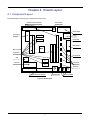
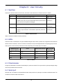
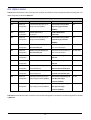
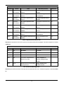
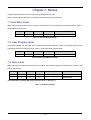
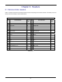
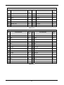
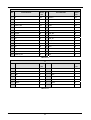
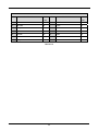
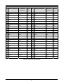
REG10J0082-0100
Renesas Starter Kit for H8S/2472
User’s Manual
RENESAS SINGLE-CHIP MICROCOMPUTER
H8S FAMILY
Rev.1.00
Revision date: 28.08.2008
Renesas Technology Europe Ltd.
www.renesas.com
Disclaimer
By using this Renesas Starter Kit (RSK), the user accepts the following terms. The RSK is not guaranteed to be error free, and the entire
risk as to the results and performance of the RSK is assumed by the User. The RSK is provided by Renesas on an “as is” basis without
warranty of any kind whether express or implied, including but not limited to the implied warranties of satisfactory quality, fitness for a
particular purpose, title and non-infringement of intellectual property rights with regard to the RSK. Renesas expressly disclaims all such
warranties. Renesas or its affiliates shall in no event be liable for any loss of profit, loss of data, loss of contract, loss of business,
damage to reputation or goodwill, any economic loss, any reprogramming or recall costs (whether the foregoing losses are direct or
indirect) nor shall Renesas or its affiliates be liable for any other direct or indirect special, incidental or consequential damages arising
out of or in relation to the use of this RSK, even if Renesas or its affiliates have been advised of the possibility of such damages.
Precautions
This Renesas Starter Kit is only intended for use in a laboratory environment under ambient temperature and humidity conditions. A safe
separation distance should be used between this and any sensitive equipment. Its use outside the laboratory, classroom, study area or
similar such area invalidates conformity with the protection requirements of the Electromagnetic Compatibility Directive and could lead to
prosecution.
The product generates, uses, and can radiate radio frequency energy and may cause harmful interference to radio communications.
However, there is no guarantee that interference will not occur in a particular installation. If this equipment causes harmful interference to
radio or television reception, which can be determined by turning the equipment off or on, you are encouraged to try to correct the
interference by one or more of the following measures;
•
ensure attached cables do not lie across the equipment
•
reorient the receiving antenna
•
increase the distance between the equipment and the receiver
•
connect the equipment into an outlet on a circuit different from that which the receiver is connected
•
power down the equipment when not is use
•
consult the dealer or an experienced radio/TV technician for help NOTE: It is recommended that wherever possible shielded
interface cables are used.
The product is potentially susceptible to certain EMC phenomena. To mitigate against them it is recommended that the following
measures be undertaken;
•
The user is advised that mobile phones should not be used within 10m of the product when in use.
•
The user is advised to take ESD precautions when handling the equipment.
The Renesas Starter Kit does not represent an ideal reference design for an end product and does not fulfil the regulatory standards for
an end product.
ii
Table of Contents
Chapter 1. Preface .................................................................................................................................................. 4
Chapter 2. Purpose ................................................................................................................................................. 5
Chapter 3. Power Supply ........................................................................................................................................ 6
3.1. Requirements ............................................................................................................................................... 6
3.2. Power – Up Behaviour ................................................................................................................................. 6
Chapter 4. Board Layout ......................................................................................................................................... 7
4.1. Component Layout ....................................................................................................................................... 7
4.2. Board Dimensions ........................................................................................................................................ 8
Chapter 5. Block Diagram ....................................................................................................................................... 9
Chapter 6. User Circuitry....................................................................................................................................... 10
6.1. Switches ..................................................................................................................................................... 10
6.2. LEDs ........................................................................................................................................................... 10
6.3. Potentiometer ............................................................................................................................................. 10
6.4. Serial port ................................................................................................................................................... 10
6.5. USB ............................................................................................................................................................ 11
6.6. Ethernet ...................................................................................................................................................... 11
6.7. Debug LCD Module .................................................................................................................................... 12
6.8. Option Links................................................................................................................................................ 13
6.9. Oscillator Sources ...................................................................................................................................... 17
6.10. Reset Circuit ............................................................................................................................................. 18
Chapter 7. Modes.................................................................................................................................................. 19
7.1. User Boot mode.......................................................................................................................................... 19
7.2. User Program mode ................................................................................................................................... 19
7.3. Boot mode .................................................................................................................................................. 19
Chapter 8. Programming Methods ........................................................................................................................ 20
Chapter 9. Headers ............................................................................................................................................... 21
9.1. Microcontroller Headers ............................................................................................................................. 21
9.2. Application Headers ................................................................................................................................... 26
Chapter 10. Code Development ........................................................................................................................... 29
10.1. Overview................................................................................................................................................... 29
10.2. Compiler Restrictions ............................................................................................................................... 29
10.3. Mode Support ........................................................................................................................................... 29
10.4. Breakpoint Support ................................................................................................................................... 29
10.5. Memory Map............................................................................................................................................. 30
Chapter 11. Component Placement ...................................................................................................................... 31
Chapter 12. Additional Information........................................................................................................................ 32
iii
Chapter 1. Preface
Cautions
This document may be, wholly or partially, subject to change without notice.
All rights reserved. Duplication of this document, either in whole or part is prohibited without the written permission of Renesas
Technology Europe Limited.
Trademarks
All brand or product names used in this manual are trademarks or registered trademarks of their respective companies or
organisations.
Copyright
© Renesas Technology Europe Ltd. 2008. All rights reserved.
© Renesas Technology Corporation. 2008. All rights reserved.
© Renesas Solutions Corporation. 2008. All rights reserved.
Website:
http://www.eu.renesas.com/
Glossary
CPU
Central Processing Unit
HEW
High-performance Embedded Workshop
LED
Light Emitting Diode
RSK
Renesas Starter Kit
PC
Program Counter
E10A
On-chip debugger module
ESD
Electrostatic Discharge
EMC
Electromagnetic compatibility
4
Chapter 2. Purpose
This RSK is an evaluation tool for Renesas microcontrollers.
This manual describes the technical details of the RSK hardware. The Quick Start Guide and Tutorial Manual provide details of the
software installation and debugging environment.
Features include:
•
Renesas Microcontroller Programming.
•
User Code Debugging.
•
User Circuitry such as Switches, LEDs and potentiometer.
•
User or Example Application.
•
Sample peripheral device initialisation code.
The RSK board contains all the circuitry required for microcontroller operation.
5
Chapter 3. Power Supply
3.1. Requirements
This RSK operates from a 5V power supply.
A diode provides reverse polarity protection only if a current limiting power supply is used.
All RSK boards are supplied with an E10A debugger. This product is able to power the RSK board with up to 300mA. When the RSK is
connected to another system then that system should supply power to the RSK.
All RSK boards have an optional centre positive supply connector using a 2.0mm barrel power jack.
Warning
The RSK is neither under nor over voltage protected. Use a centre positive supply for this board.
3.2. Power – Up Behaviour
When the RSK is purchased the RSK board has the ‘Release’ or stand alone code from the example tutorial code pre-programmed into the
Renesas microcontroller. On powering up the board the user LEDs will start to flash. After 200 flashes, or after pressing a switch the LEDs
will flash at a rate controlled by the potentiometer.
6
Chapter 4. Board Layout
4.1. Component Layout
The following diagram shows top layer component layout of the board.
Application board interface
JA5
Reset switch
JA1
RS232 Serial
LCD Display
LCD
J7
Power
J8
Power LED
J6 J5
JA3
E8A Header
MCU
Microcontroller
pin headers
J2 J1
E10A Header
USB
J3
Ethernet
User LEDs
J4
Boot LED
JA6
JA2
Application board interface
Potentiometer
Figure 4-1: Board Layout
7
User switches
4.2. Board Dimensions
The following diagram gives the board dimensions and connector positions. All through hole connectors are on a common 0.1” grid for easy
interfacing.
120.00mm
115.00mm
86.36mm
Corners x4
3mm radius
Short Board = 85 mm
50.80 mm
43.18 mm
35.56 mm
27.00mm
SW
1
SW
2
SW
3
POT
JA2
JA6
J4
J1 J2
J3
E10A
ETHERNET
J1 Applies to connector
with microcontroller pin A1
USB
J5 J6
MCU
E8A
J8
J7
PWR
Serial D9
SKT
R
E
S
JA5
JA1
45.00mm
Figure 4-2: Board Dimensions
8
Chapter 5. Block Diagram
Figure 5-1 shows the CPU board components and their connectivity.
Figure 5-1: Block Diagram
Figure 5-2 shows the connections to the RSK.
Figure 5-2: RSK Connections
9
Chapter 6. User Circuitry
6.1. Switches
There are four switches located on the CPU board. The function of each switch and its connection are shown in Table 6-1.
Switch
Function
Microcontroller
RES
When pressed, the RSK microcontroller is reset.
RESn, Pin E4
SW1/BOOT*
Connects to an IRQ input for user controls.
IRQ8n, Pin L15
The switch is also used in conjunction with the RES switch to place the device in
(Port 6 pin 7)
BOOT mode when not using the E10A debugger.
SW2*
Connects to an IRQ line for user controls.
IRQ9n, Pin L14
(Port 6, pin 6)
SW3*
Connects to the ADC trigger input. Option link allows connection to IRQ line.
IRQ10, Pin L13
The option is a pair of 0R links. For more details on option links, please refer
(Port 6, pin 5)
to Sec 6.8.
Table 6-1: Switch Functions
*Refer to schematic for detailed connectivity information.
6.2. LEDs
There are six LEDs on the RSK board. The green ‘POWER’ LED lights when the board is powered. The orange BOOT LED indicates the
device is in BOOT mode when lit. The four user LEDs are connected to an IO port and will light when their corresponding port pin is set low.
Table 6-2, below, shows the LED pin references and their corresponding microcontroller port pin connections.
LED Reference (As
Colour
Microcontroller Port Pin
shown on silkscreen)
Microcontroller
Pin Number
LED0
Green
Port F2
G13
LED1
Orange
Port F3
D4
LED2
Red
Port F4
B4
LED3
Red
Port F6
E3
Table 6-2: LED Port
6.3. Potentiometer
A single turn potentiometer is connected to channel AN0 (P7.0) of the microcontroller. This may be used to vary the input analogue voltage
value to this pin between AVCC and Ground.
6.4. Serial port
Serial port SCIF is connected to the standard RS232 header. Serial port SCI3 can optionally be connected to the RS232 header. The
connections to be fitted are listed in the Table 6-3.
10
Description
Function
Microcontroller
Fit for RS232
Remove for RS232
Port Pin
SCIF
Default serial port
G4
R31
R34
SCIF
Default serial port
F2
R30
R35
SCI3
Spare Serial Port
N5
R15, R34
R31
SCI3
Spare Serial Port
P5
R28, R35
R30
Table 6-3: Serial Port settings
The SCIF port is also available on J7/J8 and JA2. The SCI3 port is available on J5/J6 and JA6.
6.5.USB
The USB module can be used for USB communication with host.
Table 6-4 contains details of the signal descriptions and pin connections.
Description
Function
Microcontroller
Header Pins
Pin Number
VBUS
USB cable connection
J14
J3-10
monitor pin
USD+
USB data I/O pin
K14
-
USD-
USB data I/O pin
K15
-
DrVcc
Power supply pin for USB
K13
J4-14
J13
-
built-in transceiver
DrVss
Ground pin for USB
built-in transceiver
PUPDPLS
Pull-up control pin
J15
J3-9
CON_UXTAL
USB clock pin
A5
J1-9
CON_UEXTAL
USB clock pin
B5
J1-10
UXSEL
USB clock select pin
D5
J2-10
Table 6-4: USB module settings
6.6.Ethernet
The Ethernet module conforms to the Ethernet or IEEE802.3 media access control (MAC) standard. Ethernet controller is connected to the
direct memory access controller for Ethernet controller (E-DMAC) and carries out high-speed data transfer to and from the memory. In
addition, Ethernet controller is connected to SMSC LAN8700i physical layer chip enabling it to perform transmission and reception of
Ethernet frames.
Table 6-5 contains details of the signal descriptions and pin connections.
11
Description
Function
Microcontroller
Header
Pin Number
Pins
RM_REF-CLK
Transmit/Receive clock
A13
-
RM_TX-EN
Transmit enable
B12
J1-24
RM_TXD1
Transmit data, Bit 1
C11
J2-21
RM_TXD0
Transmit data, Bit 0
B11
J1-22
RM_CRS-DV
Carrier
C12
J2-23
detection/Receive data
valid
RM_RXD1
Receive data, Bit 1
D11
J2-22
RM_RXD0
Receive data, Bit 0
A12
J1-23
RM_RX-ER
Receive error
B13
J1-26
MDC
Management data clock
G15
J3-5
MDIO
Management data I/O
G14
J3-6
LINKSTA_A22
Link status
N1
J6-29
WOL
Wake-on-LAN
-
-
Table 6-5: Ethernet module settings
6.7.Debug LCD Module
A debug LCD module is supplied to be connected to the connector LCD. This should be fitted so that the debug LCD module lies over J3.
Care should be taken to ensure the pins are inserted correctly into LCD. The debug LCD module uses a 4 bit interface to reduce the pin
allocation. No contrast control is provided; this is set by a resistor on the supplied display module. The module supplied with the RSK only
supports 5V operation.
Table 6-6 shows the pin allocation and signal names used on this connector.
LCD
Pin
Circuit Net Name
Device
Circuit Net Name
Pin
Device
Pin
Pin
1
Ground
-
2
5V Only
-
3
No Connection
-
4
DLCDRS (PC5)
K3
5
R/W (Wired to Write only)
-
6
DLCDE + 100k pull down to ground (PC4)
K1
7
No Connection
-
8
No connection
-
9
No Connection
-
10
No connection
-
11
DLCDD4 (PC0)
M2
12
DLCDD5 (PC1)
L4
13
DLCDD6 (PC2)
L1
14
DLCDD7 (PC3)
K2
Table 6-6 Debug LCD Module Connections
12
6.8. Option Links
Table 6-7 below describes the function of the option links contained on this RSK board and associated with Serial Port Configuration. The
default configuration is indicated by BOLD text.
Option Link Settings
Reference
R15
Function
Fitted
Alternative (Removed)
Serial Port
Connects serial port SCI3 (Tx) to
Disconnects serial port SCI3
Configuration
D-type connector (SERIAL).
(Rx) from D-type connector
Related To
R28
(SERIAL).
R19
R28
Serial Port
Disables RS232 Serial
Enables RS232 Serial
configuration
Transceiver
Transceiver
Serial Port
Connects serial port SCI3 (Tx) to
Disconnects serial port SCI3
Configuration
D-type connector (SERIAL).
(Tx) from D-type connector
R15
(SERIAL).
R30
R31
R32
Serial Port
Routes serial port SCI0 (Rx) to
Disconnects serial port SCI0 (Rx)
Configuration
microcontroller pins.
from microcontroller pins.
Serial Port
Routes serial port SCI0 (Tx) to
Disconnects serial port SCI0 (Tx)
Configuration
microcontroller pins.
from microcontroller pins.
Serial Port
Routes serial port to JA6 pins.
Disconnects serial port from
Serial Port
Routes serial port to JA6 pins.
R35
R36
R30, R31, R33
Disconnects serial port from
R30, R31, R32
JA6 pins.
Configuration
R34
R30, R32, R33
JA6 pins.
Configuration
R33
R31, R32, R33
Serial Port
Routes serial port SCI3 (Rx) to
Disconnects serial port SCI3
Configuration
microcontroller pins.
(Rx) from microcontroller pins.
Serial Port
Routes serial port SCI3 (Tx) to
Disconnects serial port SCI3
Configuration
microcontroller pins.
(Tx) from microcontroller pins.
Serial Port
Connects programming port SCI1
Disconnects programming port
Configuration
(Rx) to D-type connector (SERIAL).
SCI1 (Rx) from D-type
R35
R34
R37, R6
connector (SERIAL).
R37
Serial Port
Connects programming port SCI1
Disconnects programming port
Configuration
(Tx) to D-type connector (SERIAL).
SCI1 (Tx) from D-type
R36, R5
connector (SERIAL).
Table 6-7: Serial port configuration links.
Table 6-8 below describes the function of the option links associated with application board interface. The default configuration is indicated
by BOLD text.
13
Option Link Settings
Reference
R56
R60
R69
R95
R96
R114
R115
R116
Function
Fitted
Alternative (Removed)
Application
Use ADTRGn of application board
Use TxD3 of application board
board interface
interface.
interface.
Application
Use AN0 of application board
Use AD_POT of application
board interface
interface.
board interface.
Application
Use HWRn of application board
Use WRn of application board
board interface
interface.
interface.
Application
Use TxD3 of application board
Use ADTRGn of application board
board interface
interface.
interface.
Application
Use AD_POT of application board
Use AN0 of application board
board interface
interface.
interface.
Application
Use WRn of application board
Use HWRn of application board
board interface
interface.
interface.
Application
Use A22 of application board
Use LINKSTA of application
board interface
interface.
board interface.
Application
Use LINKSTA of application board
Use A22 of application board
board interface
interface.
interface.
Related To
R95
R96
R114
R56
R60
R69
R116
R115
Table 6-8: Application board interface links.
Table 6-9 below describes the function of the option links associated with E8 and E10A debuggers. The default configuration is indicated
by BOLD text.
Option Link Settings
Reference
Function
Fitted
Alternative (Removed)
Related To
R4
E8
E8 enabled.
E8 disabled.
R5
E8
E8 Tx enabled.
E8 Tx disabled.
R6, R36
R6
E8
E8 Rx enabled.
E8 Rx disabled.
R5, R37
R161
E8
If J9 or R161 is fitted the Flash is
If both J9 and R161 are
protected from writing.
removed, writing to Flash is
enabled.
R203
E10A
Enables E10A, also can be enabled
E10A is disabled, can be
by fitting E10A_EN.
enabled if J5 is set.
Table 6-9: E8 and E10A debugger links.
Table 6-10 below describes the function of the option links associated with power source. The default configuration is indicated by BOLD
text.
14
Option Link Settings
Reference
R125
R126
Function
Power source
MCU power
Fitted
Alternative (Removed)
Enables power to board from
Disable power to board from
R131, R158,
E8_VCC.
E8_VCC.
R129, R130
Supply to MCU.
CPU current can be measured
supply
R127
R128
R129
Ground
Power source
Power source
Related To
across R126
Connects Analog & Digital
Separates Analog & Digital
grounds together.
grounds.
Fitted if board is not powered
Removed if board is powered from
from external source CON_3V3.
external source CON_3V3.
5V source signal will be powered
5V source signal will not be
R130, R153,
from E8_VCC.
powered from E8_VCC.
R154, R155,
R157
R156
R130
Power source
CON_5V source signal will be
CON_5V source signal will not be
R129, R153,
powered from E8_VCC.
powered from E8_VCC.
R154, R155,
R156
R131
R153
R154
Power source
Power source
Power source
Enables power to board from
Disable external power to board
R125, R158,
external source.
from connector.
R153, R154
CON_5V source signal will be
CON_5V source signal will not
R129, R130,
powered from external source.
be powered from PWR
R154, R155,
connector.
R156
5V source signal will be powered
5V source signal will not be
R129, R130,
from PWR connector.
powered from PWR connector.
R153, R155,
R156
R155
R156
Power source
Power source
CON_5V source signal will be
CON_5V source signal will not
R129, R130,
powered from VBUS connector.
be powered from VBUS
R153, R154,
connector
R156
5V source signal will be powered
5V source signal will not be
R129, R130,
from VBUS connector.
powered from VBUS connector.
R153, R154,
R155
R157
R158
Power source
Power source
Board can be powered from
Board can’t be powered from
external source CON_3V3.
external source CON_3V3.
Enables power to board from VBUS.
Disable power to board from
R125, R131,
VBUS.
R155, R156
R128
Table 6-10: Power configuration links.
Table 6-11 below describes the function of the option links associated with clock configuration. The default configuration is indicated by
BOLD text.
15
Option Link Settings
Reference
R93
Function
Clock Oscillator
Fitted
Alternative (Removed)
External Clock Source for USB
On-board Clock Source for USB
Related To
R94, R103,
R105
R94
Clock Oscillator
External Clock Source for USB
On-board Clock Source for USB
R93, R103,
R105
R98
Clock Oscillator
Parallel resistor for a crystal
Not fitted
R99
Clock Oscillator
External Clock Source
On-board Clock Source
R100
Clock Oscillator
Parallel resistor for a crystal
Not fitted
R101
Clock Oscillator
On-board clock source is used
External clock source is used
R99, R102
R102
Clock Oscillator
External Clock Source
On-board Clock Source
R99, R101
R103
Clock Oscillator
On-board clock source is used
External clock source is used
R93, R94, R105
R105
Clock Oscillator
On-board clock source is used
External clock source is used
R93, R94, R103
R199
Clock Oscillator
RM_REF-CLK signal will be
RM_REF-CLK signal will not be
available on J1 connector
available on J1 connector
R101, R102
Table 6-11: Clock configuration links.
Table 6-12 below describes the function of the option links associated with reference voltage source. The default configuration is indicated
by BOLD text.
Option Link Settings
Reference
R64
Function
Fitted
Alternative (Removed)
Voltage
Voltage Reference set to board
Voltage Reference taken from
Reference
Vcc signal.
external connector (JA1 pin 7).
Voltage
Voltage Reference is taken from
Voltage Reference set to board
Reference
external connector (JA1 pin 7).
Vcc signal.
Related To
R83
Source
R83
R64
Source
Table 6-12: Voltage reference links.
Table 6-13 below describes the function of the option links associated with analog power supply. The default configuration is indicated by
BOLD text.
16
Option Link Settings
Reference
R46
R189
R198
Function
Fitted
Alternative (Removed)
Analog Voltage
Analog voltage source from external
Analog voltage source from on
Source
connector.
board Vcc.
Analog Voltage
Analog voltage source from external
Analog voltage source from
Source
connector.
on-board Vcc.
Analog Voltage
Analog voltage source from
Analog Voltage Source from
Source
on-board Vcc.
external connector.
Related To
R198
R189
Table 6-13: Analog power supply links.
Table 6-14 below describes the function of the option links associated with MCU modes. The default configuration is indicated by BOLD
text.
Option Link Settings
Reference
R160
Function
MCU Mode
Fitted
Alternative (Removed)
MCU User Boot Mode enabled, also
MCU User Boot mode disabled
Related To
can be enabled by fitting jumper in
J10
Table 6-14: MCU mode links.
Table 6-15 below describes the function of the option links associated with switches configuration. The default configuration is indicated by
BOLD text.
Option Link Settings
Reference
R132
Function
Switches
Fitted
Alternative (Removed)
Related To
SW3 can be used for ADTRGn
SW3 can not be used for ADTRGn
R133
SW3 can be used for IRQ10n
SW3 can not be used for IRQ10n
R132
configuration
R133
Switches
configuration
Table 6-15: Switches configuration links.
6.9. Oscillator Sources
A crystal oscillator is fitted on the RSK and used to supply the main clock input to the Renesas microcontroller. Table 6-16 details the
oscillators that are fitted and alternative footprints provided on this RSK:
Component
Crystal (X1)
Fitted
8.5 MHz (HC49/4H package)
Crystal (X2)
Fitted
8 MHz (HC49/4H package)
Crystal (X3)
Fitted
50 MHz
Table 6-16: Oscillators / Resonators
17
6.10. Reset Circuit
The CPU Board includes a simple latch circuit that links the mode selection and reset circuit. This provides an easy method for swapping
the device between Boot Mode and User mode. This circuit is not required on customer’s boards as it is intended for providing easy
evaluation of the operating modes of the device on the RSK. Please refer to the hardware manual for more information on the
requirements of the reset circuit.
The Reset circuit operates by latching the state of the boot switch on pressing the reset button. This control is subsequently used to
modify the mode pin states as required.
The mode pins should change state only while the reset signal is active to avoid possible device damage.
The reset is held in the active state for a fixed period by a pair of resistors and a capacitor. Please check the reset requirements carefully
to ensure the reset circuit on the user’s board meets all the reset timing requirements.
18
Chapter 7. Modes
This RSK supports Boot mode, User Boot mode, User Program Mode and User mode.
Details of programming the FLASH memory is described in the H8S/2472 Group Hardware Manual.
7.1.User Boot mode
Refer to H8S/2472 Group Hardware Manual for details of User Boot Mode. The user mode settings for this RSK are shown in Table 7-2:
user Boot Mode pin settings below:
FWE
MD2n
MD1
NMI
1
0
0
0
LSI State after Reset End
User Boot Mode
Table 7-1: User Boot Mode pin settings
7.2. User Program mode
This is default operating mode of this RSK. Refer to H8S/2472 Group Hardware Manual for details of User Program Mode. The User
Program Mode settings for this RSK are shown in Table 7-3: User Program Mode pin settings below:
FWE
MD2n
MD1
NMI
1
1
1
X
LSI State after Reset End
User Program Mode
Table 7-2: User Program Mode pin settings
7.3. Boot mode
Refer to H8S/2472 Group Hardware Manual for details of User Mode. The User Mode settings for this RSK are shown in Table 7-4: User
Mode pin settings below:
FWE
MD2n
MD1
NMI
PF5
1
0
0
1
0*
SC1 Boot Mode
1
0
0
1
1*
USB Boot Mode
* When USB cable is plugged in USB connector PF5 will read as “1” otherwise “0”.
Table 7-3: User Mode pin settings
19
LSI State after Reset End
Chapter 8. Programming Methods
The board is intended for use with HEW and the supplied E10A debugger. Refer to H8S/2472 Group Hardware Manual for details of
programming the microcontroller without using these tools. Please note that to use E10A debugger, jumper E10A_EN must be fitted.
20
Chapter 9. Headers
9.1. Microcontroller Headers
Table 9-1 to Table 9-8 show the microcontroller pin headers and their corresponding microcontroller connections. The header pins connect
directly to the microcontroller pin unless otherwise stated.
J1
Pin
Circuit Net Name
Device
Pin
Circuit Net Name
Pin
Device
Pin
1
UC_VCC
A1
2
A14
B1
3
CON_XTAL
A2
4
CON_EXTAL
B2
5
GROUND
A3
6
RESOn
B3
7
LED3
A4
8
LED2
B4
9
CON_UXTAL
A5
10
CON_UEXTAL
B5
11
PIN_A6
A6
12
A12
B6
13
PTTX
A7
14
PTRX
B7
15
D6
A8
16
D7
B8
17
D14
A9
18
D15
B9
19
D10
A10
20
D11
B10
21
UC_VCC
A11
22
RM_TxD0
B11
23
RM_RXD0
A12
24
RM_TX-EN
B12
25
CON_RM_REF_CLK
A13
26
RM_RX-ER
B13
27
A0
A14
28
A2
B14
29
A1
A15
30
A3
B15
Table 9-1: J1
21
J2
Pin
Circuit Net Name
Device
Pin
Circuit Net Name
Pin
Device
Pin
1
WRn_HWRn
C1
2
MD1
D1
3
A15
C2
4
GROUND
D2
5
A13
C3
6
BCLK
D3
7
NC
C4
8
LED1
D4
9
UC_VCC
C5
10
UXSEL
D5
11
PIN_C6
C6
12
FWE
D6
13
NC
C7
14
GROUND
D7
15
D5
C8
16
D4
D8
17
D13
C9
18
D12
D9
19
D9
C10
20
D8
D10
21
RM_TXD1
C11
22
RM_RXD1
D11
23
RM_CRS-DV
C12
24
A5
D12
25
GROUND
C13
26
A7
D13
27
A4
C14
28
A8
D14
29
A6
C15
30
A9
D15
Table 9-2: J2
J3
Pin
Circuit Net Name
Device
Pin
Circuit Net Name
Pin
Device
Pin
1
PIN_E15
E15
2
A11
E14
3
PIN_F15
F15
4
PIN_F14
F14
5
MDC
G15
6
MDIO
G14
7
TDI
H15
8
TCK
H14
9
PUPDPLS
J15
10
VBUS_DET
J14
11
NC
K15
12
NC
K14
13
IRQ8n
L15
14
IRQ9n
L14
Table 9-3: J3
22
J4
Pin
Circuit Net Name
Device
Pin
Circuit Net Name
Pin
Device
Pin
1
PIN_E13
E13
2
A10
E12
3
GROUND
F13
4
NC
F12
5
LED0
G13
6
ETRSTn
G12
7
TDO
H13
8
TMS
H12
9
GROUND
J13
10
NC
J12
11
BOARD_VCC
K13
12
UC_VCC
K12
13
IRQ10n
L13
14
D3
L12
Table 9-4: J4
J5
Pin
Circuit Net Name
Device
Pin
Circuit Net Name
Pin
Device
Pin
1
AN6
R15
2
CON_AVCC
P15
3
AN4
R14
4
AN5
P14
5
AN1
R13
6
AN3
P13
7
NC
R12
8
CON_AVSS
P12
9
IO2
R11
10
IO1
P11
11
IO5
R10
12
IO4
P10
13
PIN_R9
R9
14
UC_VCC
P9
15
PIN_R8
R8
16
PIN_P8
P8
17
PIN_R7
R7
18
NC
P7
19
PIN_R6
R6
20
PIN_M7
P6
21
SCK1
R5
22
RxD3
P5
23
NC
R4
24
NC
P4
25
A16
R3
26
A17
P3
27
NC
R2
28
A19
P2
29
NC
R1
30
A20
P1
Table 9-5: J5
23
J6
Pin
Circuit Net Name
Device
Pin
Circuit Net Name
Pin
Device
Pin
1
D1
N15
2
IRQ11n
M15
3
CON_AVREF
N14
4
D2
M14
5
AN7
N13
6
D0
M13
7
ADPOT_AN0
N12
8
AN2
M12
9
IO3
N11
10
IO0
M11
11
IO6
N10
12
IO7
M10
13
PIN_N9
N9
14
PIN_M9
M9
15
PIN_N8
N8
16
PIN_M8
M8
17
NC
N7
18
PIN_P6
M7
19
PIN_N6
N6
20
PIN_M6
M6
21
ADTRGn_TxD3
N5
22
GROUND
M5
23
NC
N4
24
A21
M4
25
A18
N3
26
A23
M3
27
UC_VCC
N2
28
DLCDD4
M2
29
LINKSTA_A22
N1
30
NC
M1
Table 9-6: J6
J7
Pin
Circuit Net Name
Device
Pin
Circuit Net Name
Pin
Device
Pin
1
DLCDD6
L1
2
NC
L2
3
DLCDE
K1
4
DLCCD7
K2
5
NC
J1
6
RDn
J2
7
NC
H1
8
PIN_H2
H2
9
PIN_G1
G1
10
IOSn
G2
11
MD2n
F1
12
TxD0
F2
13
STBYn
E1
14
NMI
E2
Table 9-7: J7
24
J8
Pin
Circuit Net Name
Device
Pin
Circuit Net Name
Pin
Device
Pin
1
NC
L3
2
DLCDD5
L4
3
DLCDRS
K3
4
LWRn
K4
5
PIN_J3
J3
6
AHn
J4
7
EXPWX0
H3
8
EXPWX1
H4
9
CS256n
G3
10
RxD0
G4
11
NC
F3
12
NC
F4
13
PIN_E3
E3
14
RESn
E4
Table 9-8: J8
25
9.2.Application Headers
Table 9-9 to Table 9-13 below show the standard application header connections.
JA1
Pin
Generic Header Name
CPU board
Device
Signal Name
Pin
Pin
Generic Header Name
CPU board
Device
Signal Name
Pin
1
5V
CON_5V
-
2
0V
GROUND
-
3
3V3
CON_3V3
-
4
0V
GROUND
-
5
AVCC
CON_AVCC
P15
6
AVss
CON_AVSS
P12
7
AVref
CON_AVREF
N14
8
ADTRG
ADTRGn
N5
9
AD0
AN0
N12
10
AD1
AN1
R13
11
AD2
AN2
M12
12
AD3
AN3
P13
13
DAC0
NC
-
14
DAC1
NC
-
15
IO_0
IO0
M11
16
IO_1
IO1
P11
17
IO_2
IO2
R11
18
IO_3
IO3
N11
19
IO_4
IO4
P10
20
IO_5
IO5
R10
21
IO_6
IO6
N10
22
IO_7
IO7
M10
23
IRQ3
IRQ11n
M15
24
IIC_EX
NC
-
25
IIC_SDA
SDA0
P6
26
IIC_SCL
SCL0
M7
Table 9-9: JA1 Standard Generic Header
JA2
Pin
Generic Header Name
CPU board
Device
Signal Name
Pin
Pin
Generic Header Name
CPU board
Device
Signal Name
Pin
1
RESn
RESn
E4
2
EXTAL
CON_EXTAL
B2
3
NMIn
NMI
E2
4
VSS1
GROUND
-
5
WDT_OVF
RESOn
B3
6
SCIaTX
TxD0
G4
7
IRQ0
IRQ8n
L15
8
SCIaRX
RxD0
F2
9
IRQ1
IRQ9n
L14
10
SCIaCK
NC
-
11
UD
NC
-
12
CTSRTS
NC
-
13
Up
NC
-
14
Un
NC
-
15
Vp
NC
-
16
Vn
NC
-
17
Wp
NC
-
18
Wn
NC
-
19
TMR0
EXPWX0
H3
20
TMR1
EXPWX1
H4
21
TRIGa
NC
-
22
TRIGb
NC
-
23
IRQ2
IRQ10n
L13
24
TRISTn
NC
-
25
-
NC
-
26
-
NC
-
Table 9-10: JA2 Standard Generic Header
26
JA5
Pin
Generic Header Name
CPU board
Device
Signal Name
Pin
Pin
Generic Header Name
CPU board
Device
Signal Name
Pin
1
AD4
AN4
R14
2
AD5
AN5
P14
3
AD6
AN6
R15
4
AD7
AN7
N13
5
CAN1TX
NC
-
6
CAN1RX
NC
-
7
CAN2TX
NC
-
8
CAN2RX
NC
-
9
AD8
NC
-
10
AD9
NC
-
11
AD10
NC
-
12
AD11
NC
-
13
TIOC0A
NC
-
14
TIOC0B
NC
-
15
TIOC0C
NC
-
16
M2_TRISTn
NC
-
17
TCLKC
NC
-
18
TCLKD
NC
-
19
M2_Up
NC
-
20
M2_Un
NC
-
21
M2_Vp
NC
-
22
M2_Vn
NC
-
23
M2_Wp
NC
-
24
M2_Wn
NC
-
Table 9-11: JA5 Standard Generic Header
JA6
Pin
Generic Header Name
CPU board
Device
Signal Name
Pin
Pin
Generic Header Name
CPU board
Device
Signal Name
Pin
1
DREQ
NC
-
2
DACK
NC
-
3
TEND
NC
-
4
STBYn
STBYn
E1
5
RS232TX
RS232TX
-
6
RS232RX
RS232RX
-
7
SCIbRX
RxD3
P5
8
SCIbTX
TXD3
N5
9
SCIcTX
PTTX
A7
10
SCIbCK
NC
-
11
SCIcCK
SCK1
R5
12
SCIcRX
PTRX
B7
13
-
-
-
14
-
-
-
15
-
-
-
16
-
-
-
17
-
-
-
18
-
-
-
19
-
-
-
20
-
-
-
21
-
-
-
22
-
-
-
23
-
-
-
24
-
-
-
Table 9-12: JA6 Standard Generic Header
27
JA3
Pin
Generic Header Name
CPU board
Device
Signal Name
Pin
Pin
Generic Header Name
CPU board
Device
Signal Name
Pin
1
A0
A0
A14
2
A1
A1
A15
3
A2
A2
B14
4
A3
A3
B15
5
A4
A4
C14
6
A5
A5
D12
7
A6
A6
C15
8
A7
A7
D13
9
A8
A8
D14
10
A9
A9
D15
11
A10
A10
E12
12
A11
A11
E14
13
A12
A12
B6
14
A13
A13
C3
15
A14
A14
B1
16
A15
A15
C2
17
D0
D0
M13
18
D1
D1
N15
19
D2
D2
M14
20
D3
D3
L12
21
D4
D4
D8
22
D5
D5
C8
23
D6
D6
A8
24
D7
D7
B8
25
RDn
RDn
J2
26
WRn
WRn
C1
27
CS0n
CS256n
G3
28
CS1n
IOSn
G2
29
D8
D8
D10
30
D9
D9
C10
31
D10
D10
A10
32
D11
D11
B10
33
D12
D12
D9
34
D13
D13
C9
35
D14
D14
A9
36
D15
D15
B9
37
A16
A16
R3
38
A17
A17
P3
39
A18
A18
N3
40
A19
A19
P2
41
A20
A20
P1
42
A21
A21
M4
43
A22
A22
N1
44
SDCLK
BCLK
D3
45
CS2n
Board_VCC
K13
46
ALE
AHn
J4
47
WRHn
HWRn
C1
48
WRLn
LWRn
K4
49
CASn
NC
-
50
RASn
NC
-
Table 9-13: JA3 Standard Generic Header
28
Chapter 10. Code Development
10.1. Overview
Note: For all code debugging using Renesas software tools, the RSK board must be connected to a PC USB port via an E10A. An E10A
pod is supplied with the RSK product.
10.2. Compiler Restrictions
The compiler supplied with this RSK is fully functional for a period of 60 days from first use. After the first 60 days of use have expired, the
compiler will default to a maximum of 64k code and data. To use the compiler with programs greater than this size you need to purchase
the full tools from your distributor.
Warning: The protection software for the compiler will detect changes to the system clock. Changes to the system clock back in time may
cause the trial period to expire prematurely.
10.3. Mode Support
HEW connects to the Microcontroller and programs it via the E10A. Mode support is handled transparently to the user.
10.4. Breakpoint Support
HEW supports breakpoints on the user code, both in RAM and ROM.
Double clicking in the breakpoint column in the code sets the breakpoint. Breakpoints will remain unless they are double clicked to remove
them.
29
10.5. Memory Map
Figure 10-1: Memory Map
30
Chapter 11.Component Placement
Figure 11-1: Component Placement – Front view
31
Chapter 12. Additional Information
For details on how to use High-performance Embedded Workshop (HEW, refer to the HEW manual available on the CD or from the web
site.
For information about the H8S/2472 series microcontrollers refer to the H8S/2472 Group hardware manual.
For information about the H8S/2472 assembly language, refer to the H8S Series Software Manual.
Online technical support and information is available at: http://www.renesas.com/renesas_starter_kits
Technical Contact Details
America:
[email protected]
Europe:
[email protected]
Japan:
[email protected]
General information on Renesas Microcontrollers can be found on the Renesas website at: http://www.renesas.com/
32
Renesas Starter Kit for H8S/2472
User's Manual
Publication Date
Rev.1.00 28.08.2008
Published by:
Renesas Technology Europe Ltd.
Duke’s Meadow, Millboard Road, Bourne End
Buckinghamshire SL8 5FH, United Kingdom
©2008 Renesas Technology Europe and Renesas Solutions Corp., All Rights Reserved.
Renesas Starter Kit for H8S/2472
User's Manual
Renesas Technology Europe Ltd.
Duke’s Meadow, Millboard Road, Bourne End
Buckinghamshire SL8 5FH, United Kingdom