1
DG24 User's Manual
Real Time Devices
'
\
DG24 User's Manual
A User's Guide to the DG24
Digital I/O Interface
Real Time Devices Inc.
1930 Park Forest A venue
P.O. Box 906
State College, PA 16804
First Printing - April 1987
Copyright © 1987
All rights reserved
Real Time Devices, Inc.
Printed m U.S.A.
Contents
Page
Illustrations
Ill
Tables
lll
Chapter I
lnuodus;tion
1-1
Chapter 2
Installation
2-1
jumper Settings • . • . • . • • . • . . . . . •
Base Address Selection - Connector P2
Interrupt Channel Selection - Connecto; P3
Board Installation
External Connectio~; ~ C;n~~cto•r ·p4
2-1
2-1 ;
2-3
Chapter 3
3-1
Controlling the 8255 PPI
825 5 Description • . . .
Mode Selection . • . . •
Programming the DG24 .
Interrupt Considerations . . . . . . . . . .
8255 Description - Data Sheet Reprint .
8255A Functional Description . . . .
Group A and Group B Controls
Ports A,B, and C . . . . • . .
8255A Operational Description . . .
,\lode Select ion
Single Bit Set/R~s"et Fe°atu~e·
Interrupt Control Functions •
Operating Modes • . . • • • . • • • •
MODE 0 (Basic Input/Output).
MODE 0 Port Definition
MODE 0 Configurations : .
MODE 1 (Strobed Input/Output) • . .
Input Control Signal Definition .
Output Control Signal Definition
Combinations of MODE 1
MODE 2 (Strobed Bidirectional B~s • Iici) ·
Bidirectional Bus I/O Control Signai
Definition
Output Operatio~; : :
Input Operations ••.
Mode Definition Summary . . . • . • . . •
Special Mode Combination Considerations
Source Current Capability on Port B and
Port C
Reading Port. C Status
Applications of the 8255A • • • • .
2-4
2-5
3-2
3-3
3-4
3-4
3-5
3-5
3-5
3-5
3-6
3-6
3-6
3-7
3-7
3-7
3-8
3-ll
3-10
3-11
3-12
3-13
3-13
3-13
3-13
3-13
3-16
3-1 (,
3-16
3-1 (,
3-17
Page
Appendix A
Specifications
DG24 Specifications.
8255 Specifications .
Appendix B
A-1
A-3
1/0 Connector
DG24 Connector Pin Assignment •
IJG24 P4 Connector/Mating Connector
Appendix C
References
Appendix D
Warranty
ii
B-1
B-1
Illustrations
Page
2-1
2-2
2-3
3-1
DG24 Component Locations . • • .
DG24 1/0 Port Address Decode •.
Interrupt Disable jumper Positions
DG24 Block Diagram . • . • . • • .
5
6
7
8
9
10
11
12
13
14
15
16
17
18
19
20
21
22
23
24
25
8255 DESCRIPTION - DATA SHEET REPRINT
8255A Block Diagram Showing Group A and
Group B Control Functions••••• , .
Basic Mode Definitions and Bus Interface •
Mode Definition- Format •
Bit Set/Reset Format.
MODE 1 Input • • . • . . .
MODE 1 (Strobed Input) •
MODE 1 Output . • • • • • •
MODE 1 (Strobed Output).
Combinations of MODE 1.
MODE Control Word •••
MODE 2 . • . • . . • . •
MODE 2 (Bidirectional)••
MODE 1/4 Combinations .
MODE 1 Status Word Format .
MODE 2 Status Word Format .
Printer Interface• . . . . . . • . •
Keyboard and Display Interface • • • • • •
Keyboard and Terminal Address Interface
Digital to Analog, Analog to Digital •
Basic CRT Controller Interface .•
Basic Floppy Disc Interface • • . .
Machine Tool Controller Interface.
B-1
DG24 P4 Connector Pin Assignment.
4
2-2
2-3
2-4
3-1
3-5
3-6
3-6
3-7
3-11
3-11
3-12
3-12
3-13
3-14
3-14
3-14
3-15
3-16
3-16
3-17
3-17
3-17
3-18
3-18
3-18
3-18
!3-1
Tables
Page
2-1
3-1
B-1
DG24 User-Selected Options ••
PP! Registe r/DG24
1/0 Address Assignments • . . • .
DG24 P4 Connector/Mating Connector
Ill
2-4
3-2
B-1
'
Chapter 1
Introduction
The DG24 is a highly versatile digital 1/0 port for the IBM PC/XT/ AT,
or compatible, computer. The board uses the popular 8255 Programmable
Peripheral Interface (PP!) chip and provides for the control or
monitoring of 24 digital 1/0 signals. The 8255 used is capable of 10 MHz
transfer rates and therefore does not require WAIT states when using a
PC/AT. The DG24's base address is jumper selectable and interrupts are
supported.
The PP! may be configured in combinations of three basic modes of
operation: Basic 1/0, Strobed 1/0, and Bi-directional Strobed l/O.
Applications of the DG24 include instrument interfacing, event sensing,
process control, and automated testing.
All 24 digital lines, as well as +/-l2 and +5 volts, the PC's reset
signal, and digital ground, are accessible through a 40-pin header
connector at the end of the board. This connector is compatible with
Real Time Devices' XB40 1/0 extender board and XC40 expansion cable. The
XB40 consists of two 20-pin screw terminals and a prototype area. The
screw terminals allow wires to easily connect to the DG24 and the
prototype area allows development of custom application circuits. The
XC40 is a cable assembly which terminates in a 40-pin wire wrap header
connector. This connector is suitable for installation in standard perfboard material.
The software included with the DG24 provides sample programs for
controlling each of the PP! operating modes. Example CALL statements are
also included for applications requiring high-speed data transfers.
1-1
This manual has been organized into three chapters, with a group of
appendices containing reference material.
CHAPTER 1 briefly describes the DG24 operating features, 1/0
capability, and software.
CHAPTER 2 explains how to install the DG24 in your computer.
This incudes selecting the base address and interrupt capability,
and connecting signals to the 1/0 connector.
CHAPTER 3 describes how to control the DG24's PPL Detailed
specifications of the PPI are provided which explain its various
operating modes and communication with the Control Word and 1/0 perts.
Some considerations are also given if you require the use of interrupts.
APPENDICES contain technical information related to your DG24. This
includes the DG24 and 8255 PPI specifications, 1/0 connector pin-out,
and connector types. References and warranty information are also
provided.
Every effort has been made to design a quality, easy to use, yet low
cost digital 1/0 interface board. We are convinced that you will find
the DG24 to be a valuable interfacing tool for your PC.
1-2
Chapter 2
Installation
The DG24 plugs into any expansion slot, including a short slot, of an
IBM PC/XT/AT or compatible computer. It may be advantageous, therefore,
to choose an available short slot inside your computer.
The board's 1/0 address and interrupt channel are jumper selectable.
Preventing possible contention with other devices simply involves
changing three jumpers. If the board address is unjumpered or incorrect,
the DG24 will not operate. Before installing the board into your
computer the jumper selections must be made.
All connections to external signals are made through one 40 pin 1/0
connector, which can be accessed through the rear of the computer after
the board is installed.
JUMPER SE'ITINGS
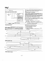
Base Address Selection - Connector P2
To select the board's base 1/0 address, the jumper on the connect er
labeled PZ must be positioned to correspond to the address desired. The
jumper should be placed horizontally across the pair of header pins
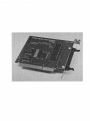
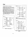
beside the base address you select (see Figure 2-1 ). The base addresses
labeled beside connector P2 are hexadecimal values.
2-1
Fig. 2-1
DG24 Component Locations
2-2
When choosing a base address, be careful not to use one that will cause
contention with another peripheral. The DG24 occupies 16 1/0 addresses
beginning with the base address selected, however only four addresses
are actually used. Chapter 3 "Controlling the 8255 PP!" explains the
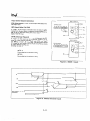
function of these four addresses. Figure 2-2 shows,how the PC's 1/0 port
address bits are decoded by the DG24.
Address
Bit
Don't Care
Base Address
Selected
AB A7
Al AC
M
PP! Register
Selected
X200
0
0
0
0
0
Port A
X240
0
0
1
0
1
Port B
c
X280
0
1
0
1
0
Port
X2CO
0
1
1
1
1
Control
X300
1
0
0
X340
1
0
1
X380
1
1
0
X3CO
1
1
1
Fig. 2-2
DG24 1/0 Port Address Decode
The DG24 base address has been preset to X'200'. For future reference,
you may wish to record the base address you selected in Table 2-1. If
the base address is changed from the preset value of X '200', the example
software provided with the DG24 will need to be modified to reflect the
new value. The procedure to do this is explained in the comments which
accompany each of the sample programs.
Interrupt Channel Selection - Connector P3
The DG24 may be configured to generate interrupts during PP! Mode 1 or
Mode 2 operation. The two PP! interrupts, INTRA and INTRB, are available
at the DG24 P3 connector and are labeled "A 11 and 11 B 11 across the top of
the connector. To select the PC interrupt channels used to service these
interrupts, position the jumpers on the connecter labled P3 to
correspond to the desired interrupt channel numbers. The jumpers should
be placed horizontally across the pair of header pins corresponding to
INTRA or INTRB and beside the interrupt channel number (see Figure 2-1 ).
Note that INTRA and INTRB must each use a separate PC interrupt channel.
If interrupts are not used, the jumpers must be positioned as shown in
Figure 2-3.
2-3
Disable
INT RB
Disable
INTRA
\
B
A
nn
~DrnJ
DD
ho
DOD
ODD
DDD
DOD
Fig. 2-3
2
3
4
5
6
7
Interrupt Disable jumper Positions
The DG24 interrupts are preset to the disabled posmon. For future
reference you may wish to record the interrupt channel assignments in
Table 2-1.
Table 2-1
DG24 User-Selected Options
1/0 Base Address
(hex)
(decimal)
INTR/IRQ Channel Selection
INTRA
IRQ
INTRB
IRQ
Chapter 3, "Controlling the 8255 PP!", describes considerations for
using the DG24 interrupts.
BOARD INSTALLATION
After selecting the base address and interrupt capability, the DG24 may
be installed inside the computer.
1. TURN OFF THE POWB:R TO YOUR COMPUTER FIRST.
owner's manual for your computer, and remove the top cover.
Refer to the
2. Select the expansion slot you wish to use and remove the
corresponding blank bracket from the rear panel of the computer.
3. Close both ejector latches on the DG24 1/0 connect er, and
orient the board inside the computer so that the connector protrudes
through the rear of the computer, and the card edge connector lines up
with the selected expansion slot connector.
2-4
4. After you are certain the board lines up correctly, push down
on the metal bracket tab and the top of the board until the board is
seated firmly in the expansion slot connector.
5. Reinstall the screw that was remove with the blank bracket and
replace the cover to your computer.
EXTERNAL CONNECTIONS - Connector P4
All external connections to the DG24 are made to the 1/0 connector,
labeled P4 (see Figure 2-1 ), which is accessible through the rear panel
of the computer after the board is installed. The P4 mating connector
type required is listed in Appendix B as well as the pin assignment of
all signals associated with the DG24.
To attach the mating connector, first open the ejector tabs on the DG24
1/0 connector. Then, observing the keying of both connectors, install
the mating connector and push firmly until the ejector tabs snap
closed, securing the connector in place.
This completes the installation; your DG24 is now properly configured.
Next, you must decide how to control the PP! for your specific application.
2-5
2-6
Chapter 3
Controlling the 8255 PPI
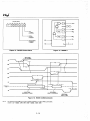
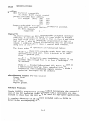
As shown in the block diagram, Figure 3-1, the DG24 provides all the
necessary interfacing signals to control the 8255 PPL
AO,Al
PORT
PAO-PA7
PBO-PB7
cs
""""
825.5
PPI
80
U)
::J
Cil
DATA BUS
D0-07
PCO-PC7
u
Q)
c:
s
u
""
RD,WR,RESET
CONTROL BUS
RESET
+/-12 Volts
+5 Volts
DIGITAL
GROUND
-=-
Fig. 3-1
DG24 Block Diagram
3-1
These signals are used to communicate with the internal registers of the
l'PI. Table 3-1 shows how the DG24 maps the PP! registers to four contiguous
J/0 addresses, beginning with the base address you selected in Chapter 2.
Table 3-1
PPI Register/DG24
1/0 Address Assignments
PP! Register
Base Address +
Port A
Port B
Port c
Control Word
0
1
2
3
The 8255 PP! is a versatile digital 1/0 interface chip; your application
will determine how the 1/0 ports should be configured and the different
operating modes selected. The accompaning data sheet, reprinted by
permission of Intel Corporation, Copyright 1981, presents a very good
discussion of controlling this chip.
8255 DESCRIPTION
The first section of the data sheet entitled "8255A Functional Description"
gives a general explanation of the 1/0 ports. This and the information
contained in the section entitled "8255A Operational lJescription" will
allow you to determine how to most efficiently utilize the 1/0 ports for
your application.
The first part of the Operational Description explains how the Control
Word is used to select the operating modes of the PPI and is also used
to individually set or reset the Port C bits. This bit set/reset feature
is useful for controlling separate bits without effecting the other bits
of Port C. The bit set/reset feature can be used with Port C bits only.
If your application requires the use of interrupts, you will also want
to read the information under the heading "Interrupt Control Functions".
This section describes how the Interrupt Enable (INTE) mask is used to
enable the INTRA and INTRB interrupt signals generated when using Modes
1 and 2.
The remainder of the Operational Description discusses the three
operating modes in detail. This information includes timing diagrams,
examples of how the operating modes may be combined, and describes the
Port C Status Word used in Modes 1 and 2. Port A and Port B source
current capabilities are also defined. Values referenced on the timing
diagrams are defined in Appendix A, "Specifications".
The section entitled "Applications of the 8255A" gives some practical
examples of how the PP! can be used for specific applications.
3-2
MODE SELECTION
Once you have decided how to define the operating modes of Ports A, B,
and C, determine the data that you will need to write to the Control
Word (refer to the "8255A Operational Description", Figure 6, of the
reprint). For example, to select:
Mode
Mode
Mode
Mode
Port A
Port B
PC 0,1,2
PC 6,7
1,
0,
0,
0,
Input
Output
Input
Output
you would write the following data:
Data
l3it
Control
Register
7
6
1
0
Data
Mode Set
Flag
4
l1
I
0
Port A,
Input
Port A,
Mode 1
0
0
II 0
1
Port B,
Mode 0
PC6,7;
Output
1
=
X'Al'
PC0,1,2;
Input
Port B,
Output
Note that PC 3 ,4, and 5 are used for the Port A handshaking and interrupt
signals and are therefore not available for 1/0 ("825 SA Operational
Description", Figure 8); however PC 0,1,2,6, and 7 can be used for
digital 1/0. The interrupt signal generated on PC 3 may be jumpered to
one of the the PC's interrupt channels. The interrupt channel selection
was described in Chapter 2.
Finally, you will need to write the data to the Control Word to select
the operating modes of the 1/0 ports. Refer to Table 3-1 to determine
the address of the Control Word. To select the operating modes used in
the above example, the data X'Al' would be written to 1/0 location
X '203' (DG24 Base Address ~ X '200' ). The following BASIC A statement will
write this data to the Control Word:
OUT
If your application will require
ports, be aware that all output
whenever the mode is changed.
into; no Read operation of the
&H203,&HA1
changing the operating modes of the l/O
registers and status flags are reset
Also, the Control Word can only be written
Control Word Register is allowed.
3-3
PROGRAMMING THE DG24
J)ue to rhe versatility of the 8255 PP!, it would not be possible to
provide utility software flexible enough for every application. However,
the software included wirh your DG24 shows some example programs for
controlling each operating mode. These programs are written in BASICA
and are extensively commented.
Also included are examples of CALL statements which are used from BASICA.
These CALL statements envoke assembly language subroutines which provide
for a more efficient and faster execution of a routine. CALL statements
would be used for high-speed data transfers. Because the 8255 used on
the DG24 is capable of 10 MHz transfer rates, WAIT states are not required
when using a PC/AT machine.
A directory of the software included with your DG24, as well as a brief
description of each program, is listed in the file README.DOC on the
Program Disk.
INTERRUPT CONSIDERATIONS
The interrupts generated in PP! Mode 1 arid Mode 2 operation may be
jumpered to any of the PC interrupt channels 2-7. The channel selection
is made by jumpering pins on the DG24 P3 connector as explained in the
Interrupt Channel Selection description in Chapter 2.
The PP! interrupts must be enabled by writing a "1" to the INTE mask bit
as described in the data sheet reprint section entitled "8255A Operational
Description" Interrupt Control Functions. The INTE mask bits are disabled
during power up reset a:ncrwhenever the PP! mode is changed.
Before you attempt to use interrupts, be certain you are familiar wirh
the procedure for intializing the interrupt vectors and the PC's interrupt
controller, and setting up the interrupt handling routines. Reference 1
in Appendix C contains a very good description of the PC's system interrupts.
3-4
8255 DESCRIPTION - DATA SHEET REPRINT
inter
Ports A, B, and C
8255A FUNCTIONAL DESCRIPTION
The B255A contains three 8-blt ports (A, 8, and C) All
can be configured In a wide varlety of functional characteristics by the system software but each has Its own
special features or "personality" to further enhance the
power and flexibility of the S255A.
Group A and Group B Controls
The functional configuration of each port is programmed by the systems software. In essence, the CPU "outputs .. a control word to tha 8255A The control word con~
talns Information such as "mode", "bit set", "bit reset",
etc., that Initializes the funcllonal configuration of the
S255A.
Each of the Control blocks (Group A and Group
Bl accepts
"commands" from the Read/Write Contr~I Logic, receives
"control words" from the internal data bus and issues the
proper commands to its associated pons.
Control Group A - Port A and Port C uoper (C7-C4t
Control Group B - Port Band Port Clower tC3-COJ
Port A. One 8-bil data output latch/buffer and one 8-bi1
data Input latch.
Port B. One 8-blt data Input/output latch/buffer and one
8-bit data input buffer.
Port C. One 8-bll data output latch/buffer and one B·bit
data Input buffer (no latch for input). This port can be
divided Into two 4-blt ports under the mode control.
Each 4-blt port contains a 4-bit latch and it can be used
for the control signal outputs and status signal lnpuls in
conjunction with ports A and B.
The Control Word Register can Only be written into. No
Read operation of the Contra! Word Register is allowed.
PIN CONF1GURATION
'"
""1·0.:.
PIN NAMES
o, o.
OATA l!ll.15 18! OIREC.HO,..._ll 1
Rl"UTllllPUT
CHIP $£Lf.C:T
REAOllllPUT
WAITE I N l ' U T _ _ _ , ;
1--.,-.-.,-,.-,,..,~.~,~.o~o=Rt~
'
,...,,..~.~...~i--:;::.,:~~~;-;:--- _, -- '
1--"'-·'~"'~•_,_-"',..."~'_c.c'8:~-"- - - - ·
\o'ct
Figure 4. S225A Block Diagram Showing Group A and
Group B Control Functions
3-5
•!.VOL 15
8255A OPERATIONAL DESCRIPTION
Mode Selecllon
COlllTAOL WORD
There are three basic modes of operation that can be selected by the system software:
Mode 0 - Basic Input/Output
I°' I L.J°' I I I I I•· I
0
•
0
•
0
•
0
•
0
•
Mode 1 - Strobed l nput/Output
Mode 2 - Bi-Directional Bus
I
When the reset input goes "high" all ports will be set to
the input mode (I.e., all 24 lines will be in the high Im·
pedance state). After the reset is removed the 8255A can
L.
remain in the Input mode with no additional inltialization
required. During the execution of the system program
any of the other modes may be selected using a single
output instruction. This allows a single 8255A to service
a variety of peripheral devices with a simple software
maintenance routine.
GROl.H'B
\
PORT C ILOWEAI
I• JNPVT
O•OVTl"IJT
l'QRT B
1 •INPUT
Q •OUTPl/T
~---
MODE
SELECTION
O•MOOEO
l•lolOOE1
The modes for Port A and Port B can be separately defined.
while Port C is divided into two portions as required by the
Port A and Port B definitions. All of the output registers, in·
c_luding the status flip-flops, will be reset whenever the
mode is changed. Modes may be combined so that their
functional definition can be "tailored" to almost any 1/0
structure. For instance; Group B can be programmed in
Mode 0 to monitor simple switch closings or display computational results, Group A could be programmed in Mode 1
to monitor a keyboard or tape reader on an interrupt-driven
I
GROUP A
'
\
POAT C !V""UI!
t •INPUT
O•Ol.lll'VT
POAT ,r.
1 •IN'1J'T
O•QUlPUT
MOOE SELECTION
OO•MOD~O
basis.
01•MOOE1
Hl·MOOE 2
MOOE $ET FLAG
1 • ACTl\IE
I
Figure 6. Mode Definition Format
MODE l -4L,;•!,,-.....i;;::;:;;;;;;;:::;::;:;;:;::r---,~',--If
Bfo Ill!
PBrPBu
1111
CONTROL
CONTROL
ORl!D
ORllO
So
P4,-PAo
MOOE2---fL~'!,,--1:;::;::;::;::=:::::;:;;::;:r-_,~·,...JT
tfuo
PS.,-P8v
111 l ·1111
f/O
'---,---I
~to'"'"'o••L
The mode definitions and possible mode combinations
may seem contusing at first but after a cursory review of
the complete device operation a simple, logtca1 1/0 ap.
proach wlll surface. The design of the 8255A has taken
Into account lhlngs such as efficient PC board layout.
control signal definition vs PC layout and complete
functional flexibility to support almost any peripheral
device with no external logic. Such design represents
the maximum use of the available pins.
PA,-Pf..o
CONTROL
Single Bit Set/Reset Feature
Any of the eight bits of Port C can be Set or Reset using a
single OUTput instruction. This feature reduces-&oftware
requirements in Control·based applications.
Figure 5. Basic Mode Definitions
and Bus Interlace
3-6
inter
When Port C is being used as status/control for Port A or 8,
these bits can be set or reset by using the Bit Set/Reset operation just as if they were data output ports.
CONTROi.. WOflO
Interrupt Control Functions
When the 8255A is programmed to operate tn mode 1 or
mode 2, con trot signals are provided that can be used as
Interrupt request inputs to the CPU. The interrupt re·
quest signals, generated from port C, can be inhibited or
enabled by setting or resetting the associated lNTE flip·
flop, using the bit set/reset function of port C.
This function allows the Programmer to disallow or allow a
specific l/0 device to interrupt the CPU without affecting
any other device in the interrupt structure.
INTE flip-flop definition:
(BIT-SET} - INTE is SET - Interrupt enable
(SIT·RESET) - INTE is RESET- interrupt disable
Note: All Mask
Figure 7. Bit Sel/Reset Format
flip~flops
are automatically reset during
mode selection and device Reset.
Operating Modes
Mode 0 Basic Functional Definitions:
MOOE 0 (Basic lnpuVOulpul). This functional configuration provides simple input and output operations for
each of the three ports. No "handshaking" is reQulred,
data Is simply written to or rean from a specified port.
•
•
•
Two 8"bit ports and two 4·bit pon:s.
Any pon can be input or output.
Outputs are latched.
•
Inputs are not latched.
•
16 different Input/Output configurations are possible
in this Mode.
o,o,---------~'•o-~..___.,.l-,o-,-==:'.f __ _
MODE 0 (Basic Input)
-------------~ 1---
i... ...
____ ,,________,
,_
C$, Al, AO
OUTPUT
r---MODE O (Basic Output)
3-7
-lwe- ___ .J
MODE 0 Port Definition
--A--T-·B
o,
GROUP A
'
GROUPS
PORT C
#
PORTS
PORTC
I LOWER)
OUTPUT
0
OUTPUT
OU!PUT
OUTPUT
1
OUTPUT
INPUT
OUTPUT
OUTPUT
2
INPUT
OUTPUT
OUTPUT
OUTPUT
INPUT
INPUT
0
OUTPUT
INPUT
J
4
OUTPUT
OUTPUT
1
OUTPUT
INPUT
5
OUTPUT
INPUT
0
OUTPUT
INPUT
6
INPUT
OUTPUT
Do
PORT A
04
03
0
0
OUTPUT
0
D
0
0
0
0
1
OUTPUT
0
1
0
0
0
1
1
0
1
0
0
1
0
0
1
1
!UPPER/
0
1
1
1
OUTPUT
INPUT
7
INPUT
1NPUT
1
0
0
0
INPUT
OUTPUT
8
OUTPUT
OUTPUT
1
0
0
1
!NPUT
OUTPUT
9
OUTPUT
INPUT
1
0
1
0
INPUT
OUTPUT
10
INPUT
OUTPUT
1
0
1
1
INPUT
OUTPUT
11
1
1
0
0
INPUT
INPUT
12
1
1
0
1
INPUT
INPUT
13
OUTPUT
INPUT
1
1
1
0
INPUT
INPUT
14
INPUT
OUTPUT
1
1
1
1
INPUT
INPUT
15
1NPU~ -~
'
i
.
INPUT
1NPUT
OUTPUT-~
OUTPUT-
MODE o Configurations
CONTROl l'l'ORD "2
CONTROL WORD uO
0.,
~DeD~D·D]D]O,Do
I' I I, I, I I I , I, I
0
0
01
05
o,
D)
0
DI
9255.A
D7 °D 0
'
B
P!::'.7·PC•
0,·Do
o,
B
...,~,,
.
.
.
'~"""o
~·l"C,
'S·'<o
' ..., ..,
.
CONTROL WORD IQ
o,
o,
0
0
o,
I, I I I I
0
Ot
I, I
'<,·""
CONTAOLWOflD'11
o,
'
..... .
c{
A~PArPAu
.
c{ .
01
D1
I, I, I, I I, I
0
0
o,
o,
o,
o,
' , I,I
i
,I
A
o,
o,
o,
o,
0
'
PAy-l'Aa
•
PC,·PC~
0
0
0
c{
'
o,
o,
.
...,....,
3-8
l"A.,.PA.c
~·l'C4
0 1. o u - - - -
-P--"S·PC,
.
.
c{ .
. . ..,""'..,""
..... .
12SSA
D1Do----
o,
I' I I I I I, i' I· I
.
intef
t255A
D1
o0
HSSA
-----
CONTROL WORD ...g
CONTROL WORD irS
Or
o,
05
o,
01
02
01
00
I• Io Io 'Io I I ! 'I
0
1255A
0
1255A
I
'~
0,011 - - - -
CQNTROL ll'IOAO
o,
o,
o~
L
~
o.
OJ
Di
01
Do
I• I Io I I• Io I' I I
0
0
0
o,.oo----
CONTROL WORD ,,7
CONTROL WORD o111
01
n1
D~
0•
OJ
01
01
00
I• Io I 'Io Io I• I• I
0
125.SA
1255A
B - F - P B 1 PB 0
3-9
CONTROL WORD #14
CONTROL WORD #U
~D1
.....
A
'{
.
.
D1
D~D3
02
o0
o1
I· I, I, I I I, I , I· I
PA,·PAo
-P-
•
.
,__,__..,....,
CCNTPIOL WOAD •11
CONTROL WQRD •13
171~1~1?171~1:1~1
......
A
'{
•
.
.
.
.
. .
.
c{ .
. .
.,...
.., ....
Operating Modes
Mode 1 Basic Functional Definitions:
MODE 1 (Strobed lnpuUOutpul). This functional con·
figuration provides a means for transferring 110 data to
or from a specified port In conjunction with strobes or
"handshaking" signals. In mode 1, port A and Port Buse
the lines on port C to generate or accept these "hand·
shaking" signals.
• Two Groups (Group A and Group 8)
• Each group contains. one 8-bit data port and one 4-bit
control/data port.
• The 8-bit data port can be either input or output.
Both inputs and outputs are latched.
• The 4-bit port is used for control and status of the
8-bit data port.
3-10
Input Control Signal Definition
STB (Strobe Input). A "low" on this Input loads data Into
the Input latch.
CONTROL WORO
o1 0. o5
IBF (Input Buffer Full F/F)
A "high" on this output indicates that the data has been
loaded into the input latch; in essence, an acknowledgement
IBF is set by STB input being low and is reset by the rising
edge of the RD input.
o~
DJ 0 2 0 1
o0
I •I •I •I , l•mCXJXtxJ
L~e;~PUT
0- OUTPUT
INTR (Interrupt Request)
A "high'' on this output can be used to interrupt the CPU
when an input device is requesting service. JNTR is set by
MODE 1(PORT8)
the STB is a ..one", IBF is a "one" and INTE is a "one".
It is reset by the falling edge of RD. This procedure allows
an input device to request service from the CPU by simply
strobing its data into the port,
INTE A
Controlled by bit set/reset of PC 4 .
INTE B
Controlled by bit set/reset of PC 2.
Figure 8. MODE 1 Input.
--- ... --m
-
.•.
1S t ! -
- - 1 !'1l6
INTR
IN,UT J'ROM PU"'kERAL.
_
-
1------•.. -----1
Figure 9. MODE 1 (Strobed Input)
3-11
Output Control Signal Definition
MODE 1 fPOfl:T Al
OBF (Output Buffer Full F/F). The OBF output will go
•·tow" to indicate that the CPU has written data out to
the specified port. The OBF F/F will be set by the rising
edge of the WR input and reset by ACK Input being low.
ACK (Acknowledge Input). A "low" on this input Informs
the 8255A that the data from port A or port B has been accepled. In essence, a response from the peripheral
device indicating that it has received the data output by
the CPU.
MODE I 1PQRl' Bl
INTR (lnlorrupl Request). A "high" on this output can be
used to interrupt the CPU when an output device has accepted data transmitted by the CPU. INTR is set when
ACK is a "one", OBF is a "one" and INTE ls a "one". It is
reset by the falling edge of WR.
INTE A
Controlled by bit set/reset of PCs.
INTE B
Controlled by bit set/reset of PC 2.
Figure 10. MODE 1 Output
WA
!---------- 1 .-..01~--------i
I
60F
1+---+----
l'<r------~1)
//
/),.._
.......-+-~--~_,.~/-·'_,....___,I
_t,,lf
ACI(
Figure 11. Mode 1 (Strobed Output)
3-12
intef
Combinations of MODE 1
Port A and Port B can be individually defined as input or
output in Mode ·1 to support a wide variety of strobed 1/0
applications.
'''•
CDNT"OL WORD
0 1 C1
0s
PC,
0 1 0 1 Dz 0 1 Dq
I •I• I , I • It I• [XJ
CONTROL WOflD
INTR..,
'
rc,. 1 --f-1.10
"'"
I
•!~PUT
,.,,--;;a_
"'•
....
"ORT A - 1snmeeo tNPUT1
PQllT 1!1 - !STROBED OUTPUT!
PORT A - I.STROBED OUTPUT!
'°RT 8 - \STROBED INPUT)
Figure 12. Combinations of MODE 1
Operating Modes
Oulput Operations
MODE 2 (Strobed Bldlrecllonal Bua UO). This functional
configuration provides a means for communicating with
a peripheral device or structure on a single 8-bit bus for
both transmitting and receiving data (bidirectional bus
r/0). "Handshaking" signals are provided to maintain
proper bus flow discipline In a similar manner to MODE
1. Interrupt generation and enable/disable functions are
also available.
OBF (Output Buller Ful). The OBF output will go "low"
to indicate lhal the CPU has writlen data out to port A.
MODE 2 Basic Funcllonal Definitions:
• Used in Group A only.
• One 8·bit, bi-directional bus Port (Pon A) and a 5·bit
control Port {Port C).
• Both inputs and outputs are latched.
• The 5-bit control port (Port C) is used for control
and status for the 8-bit, bi·directional bus pon (Port
Al.
INTE 1 (The INTE Flip-Flop Aaooclaled wllh OBF). Controlled by bit seUreset of PC6 .
ACK (Acknowledge). A ··1ow" on this Input enables the
tri-state output buffer of port A to send out the data.
Otherwise, the output buffer will be in the high im·
pedance state.
Input Operations
STB (Strobe Input}
STB (Strobe Input). A "low" on this Input loads data into
lhe input latch.
Bidirectional Bus 1/0 Conlrol Signal Definition
IBF (Input Buller Full FIF). A "'high" on this output in·
dlcates that data has been loaded into the input latch.
INTR (Interrupt Request). A high on this output can be
used to interrupt the CPU for both input or output operations.
INTE 2 (The INTE Flip-Flop Associated with IBF). Con·
trolled by bit seUreset of PC,.
3-13
intef
CONTROL WORD
PC,.
1 •fNPUT
O•OUTl'llT
f'OATB
1•LNl>UT
O•OUTPVT
...
' - - - - - G A O . _ . I MOOE
O•MODEO
1•MODE1
1!11---
Rgure 13. MODE Control Word
..,.
Rgure 14. MODE 2
....
lNTR
m
PERIPHERAL _ _ _ -
-
-
-
-
-
-
BUS
DA"\'AF"Olll
U514TO-
Figure 15. MODE 2 (Bldlrecthmal)
NOTE:
Any sequence where WR occurs before ACK and STB occur' before RO ii permiuible,
ONTR • IBF • MASK• STB •RO+ OBF • MASK• ACK• WA l
3-14
MODE 2 AND MODE 0 (lNPUTJ
f'A 1 PA 0
MODE 2 ANO MODE 0 (OUTPUT)
~
-oaF,.
I~, l~·m '1 ~sl
U 7 De
00
O'C,---sTB,.
D~
0•
o 1 0 1 D, De
I ' ! ' tXk<0 '1°31
""'"
""''
1 •INPUT
l •lNPUT
'
---f-
RO---
.., ___
WA---
WR---
PC1 <i
f/0
I
1--------+-----J
i
MOOE 2 ANO MOOE l !OUTPUT)
MOOE 2 ANO MODE 1 !INPUT)
.P'CJ
D7
I• I• l, !,, L,I, I L' l
0
""·
51-B.,
""
18F.,
"°'
Wa
o!
o~
o. o 1
o~
INTR,,
01 00
I, H<r><!XJ •I •l><J
..,---re~A
..,...
::---::~I
e< 0 - - - I N T R 1
WR---
Figure 16. MODE
3-15
I
v. Combinations
~----"'-·_,
- - '""•
I
I
Mode Definition Summary
MOOED
IN
MODE2
MOOE 1
IN
OUT
PAQ
IN
OUT
IN
OUT
PA1
IN
OUT
IN
OUT
PA2
IN
IN
OUT
IN
IN
OUT
PA3
P1\4
PA5
PAt;
PA7
PBo
PB1
P82
OUT
IN
IN
IN
IN
OUT
IN
IN
IN
OUT
OUT
OUT
OUT
OUT
PB3
IN
OUT
PS.,
IN
IN
OUT
OUT
IN
IN
PB5
PB5
PB7
OUT
IN
IN
OUT
------
OUT
OUT
OUT
---
OUT
OUT
OUT
IN
IN
OUT
OUT
MOOEO
-----
OUT
OUT
OR MODE 1
ONLY
J
•Co
IN
OUT
INTR9
INTRs
PC1
IN
OUT
1BF9
OBFe
OUT
STBa
ACK.9
PC3
IN
IN
1/0
1/0
1/0
OUT
INTRA
INTRA
INTRA
PC4
IN
OUT
STBA
OUT
IBF_A
PCfi
IN
IN
1/0
1/0
STBA
PC5
OUT
IN
OUT
ACK.A
OiFA
ACKA
PC7
1/0
1/0
PC2
Special Mode Combination Considerations
There are several combinations of modes when not alt of the
bits in Part C are used for control or status. The remaining
bits can be used as follows:
If Programmed as Inputs-
IBFA
OBFA
allows the programmer to test or verify the "status" of each
peripheral device and change the program flow accordingly.
There is no special instruction to read the status information from Pon C. A normal read operation of Port C is
executed to perform this function.
All input lines can be accessed.during a normal Port C
read.
If Programmed as Outputs Bits in C upper (PC7·PC4J must be individually accessed
using the bit set/reset function.
1
---
OUT
IN
IN
IN
OUT
GROUP A ONLY
OUT
IN
IN
IN
IN
IN
OUT
---
OUT
IN,UT CONFIGURATION
D1
D~
Dt
I I I1BF~ I
110
t/O
0,
1NTEA
D1
j
1NTR~
I
Source Current Capability on Port B and Port C
Any set of !!.sh! output buffers, selected randomly from
Ports B and C can source lmA at 1.5 volts. This feature
allows the 8255 to directly drive Darlington type drivers
and high-voltage displays that require such source current.
Reading
a!
De
1eF, /1NTR•I
-··-·-·-·-'
"'---~----------'
GROUP A
Bits in C lower IPC3-PC 0 ) can be accessed using the bit
set/reset function or accessed as a threesome bv writing
into Port C.
01
D1
!NH
GROUP IJ
OUT,UT CONFIGURATION
D1
~
I~. 11Nn. [
~
110
~
j
Di
02
01
~
!1NTA,.[ 1NrE.j imr, l1Nrn 1 J
.-------'
OROU,I
Figure 17. MODE 1 S1atua Word Formal
Port C Status
ln Mo_de 0, Port C transfers data to or from the peripheral
device. When the 8255 is programmed to function in Modes
1 or 2, Port C generates or accepts "hand-shaking" signals
with the peripheral device. Reading the contents of Port C
'
: (;
GROUP A
_____ GROUP 8
{Dl:FINEO BV MODf'Q OR lllQDE 1 SELECTION!
Figure 18. MODE 2 Status Word Formal
intef
ml
INTERRUPT
APPLICATIONS OF THE 8255A
A£QU
-r
The 8255A Is a very power1ul tool for Interfacing
perlpher.9.1 equipment to the microcompute r system. It
represents the optimum us-e of avallable pins and Is flex!ble enough 10 Interface almost any J/O device without
the need tor additional external logic.
Each perlpheral device in a microcompute r system
usually has a "service routine" associated with it. The
routine manages the software Interface between the
device and the CPU. The functional deflnitron of the
8255A Is programmed by the 110 service routine and
becomes an extension of the system sortware. By examlrilng the lfO devices Interface characterlstlc s for
both data lransfer and timing, and malchlng this information lo the examples and tables In the detailed operational description. a control word can easily be devel·
oped to initialize the 8255A to exactly "fit" the application. Figures 19 through 25 present a few examples of
typical applications of the 8255A_
r°PAi,
PCl
,.,
,,
,., - - '•'•
MOOE 1
(INPUT)
.....
MOOl"I
IOVTf'UTJ
...
""·
ec,
ACK
f.e,
.
,.,...""'
""•
""•
""•
_l'C7
SHIFT
STROBE
.,.,•,
...,
...
!3URAOUGH$
SELF-SCAN
DISPLAY
BACKsPACE
Cl.EAR
DATA READY
AC<
BLANKING
CANCEL WOHO
UPT_J
INTER A
REQUEST
Ht(OH.$11'ff0
PFUHT(ll
.l
IOU'T'VTJ
CONTROL
'"•
"'•,
'"•
~
MOOll
,.,
PA.e
MOOE I
...
........,
.....
FULLY
OECOOEO
KEV80ARO
"•
!OUT~UTI
~,
..,,,,
Figure 20. Keyboard and Dlspley Interface
"'•
........
.
...•....,
.
..,
.,
.,
.......,
....
...
......
FUllY
D!COOEO
U"WIJOARD
....
...
..
"'•
INUftlllWT
'"'""'
MOO( D
rrllll'UT1
......
.,
.......,
......
Figure 19. Printer Interface
Figure 21. Keyboard and Terminal Address
lnterfaca
3-17
"'•
..
""""
IOUUUTl
12·!1T
CONVERTUI
!DI.ti
'"
r"""·
SE"t'/'IHE;Tl
"'•
"'•
..
11n
COtlVERTER
·~·
Figure 22. Digital to Analog, Analog to Dlgltai
Figure 23. Basic CRT Controller Interlace
l'-ITUOtUPT
11EQUUT
CATC'Qt.IHIOllHI
•CMAAACTtRGfl'I
• ftE!'fl[SHBUfFtR
"" .....,
..
.....,
ILfVH
,
•CURSOR CONTROL
l"Al"EA
lAPt
REAOEA
...
:;~~~T~
{" · · -
PC,..---·--~-
'""'"'~
l!MITUNSORIH/'111
"'• - - - OUTOffLUID
"•
1"15,
PB~
--·-LH11fUGHT
---Ul"/DO'l'jf!I
' " - - - 1-lOP. SHPSTR09l
"·
PD~
'11 1
----~~
Figure 24. Basic Floppy Disc Interface
__________
- - - - - - fLUIO (NA8Lf
- - - f,,.EACfNCYSIOP
_,
Figure 25. Machine Tool Controller Interlace
Appendix A
Specifications
DG24
SPECIFICATIONS
Interface
IBM PC/XT/AT compatible
No PC/AT WAIT states required
jumper-selectable base' address
1/0 mapped: (h~x) 200 ' 300
340
240
380
280
3CO
2CO
Jumper-selectable interrupts
Both 8255 interrupts (INTRA,INTRB) are provided.
PC IRQ channels
2 - 7
supported:
Digital 1/0
The DG24 utilizes an 8255 programmable peripheral interface
(PP!) chip. It provides 24 digital I/O lines which are divided
into three 8-bit ports: A, e, and C. Port A, Port B, and each
half of Port C may be individually programmed as input or
output. In addition, strobed I/O operations may be performed
using some of the Port C lines to control data transfers.
The three modes of operation are summarized below:
Mode 0 -- Basic 1/0; provides simple input and output
operations for each port. Data is written to or read
from a specified port.
Mode 1 -- Strobed 1/0; uses handshaking signals to
transfer data through Port A or Port B. Interrupts may
be utilized.
Mode 2 -- Strobed Bidirectional 1/0; Port A is used as
a bidirectional data bus. Data transfers occur in
conjunction with handshaking signals similar to Mode 1
operation. Interrupts may be utilized.
Miscellaneous Outputs (PC-bus sourced)
Reset Driver
+S Vdc
+/-12 Vdc
Digital ground
Software Features
Sample BASICA programs are provided which demonstrate the control of
each of the PP! operating modes. Example CALL statements are also
included to show how the 8255 may be used for high-speed applications.
A complete directory of all software included with the DG24 is
listed on the accompanying disk.
A-1
Electrical
Current requirements:
+5V
20 mA
Mechanical
Connectors:
40-pin, right angle, shrouded male header with ejector tabs
Edge-connector -- IBM PC/XT/AT compatible
Environmental:
Operating temperature:
Storage temperature:
Humidity:
0 to +50 deg. Centigrade
-20 to +70 deg. Centigrade
0 to 90%, non-condensing
Size:
3.875" X 4.500"
Options:
XB40 Expansion Board
XC40 Expansion Cable
(Short slot)
Warranty: 1 year
/\-2
8255
SPECIFIC/\ TIO NS
ABSOLUTE MAXIMUM RATINGS•
o"c
Ambient Temperoture Under Bias
Storage Temperature
Voltage on Any Pin
With Respect to Ground
Power D1ss1patjo·n
-65°C
10
7o"c
+ 15Q"C
-0.5V to +7V
2501 m\\I
D.C. CHARACTERISTICS
Symbol
tO
'NOTICE: Stresses above those listed under "Absolute
Maximum Ratings" may cause permanent damage to the
de11ice. This is a stress raring only and functional opera!ion of the device at these or any other conditwns above
those indicated 1n rhe operational sections of this spec1f1·
cation rs not implied. Exposure to absolute maximurn
rating conditions for extended periods may affect device
rel1abtl1ty.
(TA""- O"C to 70"C. Vee= +SV ~ 5%, GNO"" OV)
Parameter
Min.
Max.
Input Low Voltage
-0.3
0.8
V1H
Input High Vo!tage
2.2
Voe IDBI
Output Low Voltage (Data Bus)
"-
VIL
v
v
v
v
v
v i
5.5
OA5
OAS
Voc(PER) Output Low Voltage Wer1pheral Port}
VoHIDBI
Output High Voltage [Data Busl
VoHIPERI Output High Voltage (Peripheral Port)
1
2A
I
4"2
-LO
Test Conditions
Unit
~""
I
loL""' 2.5mA
loL
~
l.7mA
I
loH '-400µA
loH "'-lOOµA
-5 0
mA
5.0
mA
l1L
Input Load Current
±lO
µA
V1N =Vee to OV
IOFL
Output Float Leakage
± 10
µA
VoUT "' Vee to OV
!oAAfll
Darlington Drive Current
Ice
Power Supply Current
'
I
R EXT -=1. 1K11:; VEXT"" l .5V
-
NOTE:
L Available on any 8 pins trom Port Band C.
CAPACITANCE
(TA= 25°C, Vee, GND = OV)
Parameter
Symbol
C1N
Input Capacitance
C110
1/0 Capac1t:rnce
I
I
Min.
Ty;---TMax.
Unit
I
10
pF
_l_
20
pF
I
A.C. CHARACTERISTICS
Test Conditions
Unmeasured prns returned to GN~
(TA= 0°C to 70°C. Vee = +sv"' 5%. GND = OV)
Bus Parameters
READ
Symbol
Parameter
Min.
Max.
Unit
'AR
Address Stable Before A EAD
0
ns
tRA
Address Stable After R EAO
0
ns
IRA
READ Pulse Width
1RO
Data Valid From R EAOl 11
toF
Data Float After READ
IRV
Time Between REAOs and/or WA !TEs
150
ns
100
0
A-3
150
40
=J
fc = 1MHz
ns
ns
ns
A.C. CHARACTERISTICS (Continued)
WRITE
Symbol
Parameter
Max.
Min.
Unll
IAW
Address Stable Before WA !TE
0
m
IWA
Address Stable After WR IT E
20
ns
tww
WAITE Pulse Width
)20
ns
tow
Data VaVid to WRITE IT. E.1
100
ns
two
Data Valid After WRITE
30
ns
OTHER TIMINGS
Symbol
Parameter
WR
11R
Peripheral Data Before RD
=
Min.
Max.
1 to Outputl I!
twe
350
0
I
Unit
ns
m
lHR
Peripheral Data After RD
0
m
lAK
ACK Pulse Width
300
ns
lST
STB Pulse Width
350
m
lp5
Per. Data Before T_E of STB
0
ns
!pH
Per. Data After T.E. of STB
!AD
ACK = 0 to Output! l l
IKD
ACK= 1 to Output Float
twos
WR
150
ns
20
=1 to OBF =ol 11
300
m
250
ns
JOO
"'
tAOB
ACK=OtoOBF= 11 11
350
ns
ts1e
STB =Oto IBF • 11 1 1
350
RD= 1 to IBF
"'
tRIB
1R!T
RD= 0 to INTR
ts1T
STB = 1 to INTR
tAIT
ACK= 1 to
twlT
WR= U to INTR = ofl.31
=0111
=01 11
= 1111
INTR = 1111
300
i
-
n<
400
ns
300
"'
350
450
ns
"'
NOTES:
1. Test Conditions: CL'"' 150pF.
2. Period of Reset pulse must be at least 50µs during or after power on Subsequent Reset pulse can be 500 ns min.
3. lNTAt may occur as early as
WA.t
A.C. TESTING INPUT, OUTPUT WAVEFORM
A.C. TESTING LOAD CIRCUIT
INPUTIOVTPUT
DEVICE
UNDER
TEST
l.•
IC,-lDOpF
>TEST POINTS<
•c TEs:1NG !NPUTSARE.0R1Vf:NtiT24VFOnAlOGIC 'A>JQO~SVF~OR.
A LOGIC () TIMING MEASUREMENTS ARE MADE AT 2 DY FOR A LCJGIC l
<I.NO 0 BY FOR A LOGIC 0
~---·---------------
·v, 11 iS SF r AT VARIOUS VOL TAG(S
SPE:CIFICATION
OURlt~G
l(STING TO GUARANTEE lHE
!L __ _ _ _ _ _ _ _ _ _ _
-------~
WAVEFORMS
MODE 0 (BASIC INPUn
. :-ri
-
Cl.Al.AO
0,0 0
1--·-.-1_
'"" - - - 1 - - - - - - -
f-1~_
-~'=-·.,~I
L
.
--------1<1--=--'•o - X
-I
MODE 0 (BASIC OUTPun
A-5
I
.,,~t--
WAVEFORMS (Continued)
MODE 1 (STROBED INPUT)
,_,_J~·
r--'lllTJ''-----J-----+----1
INl'UT FROM PERIPHERAL
-
_
MODE 1 (STROBED OUTPUT)
·IHTR
---4----1.,n
I
---OUT'11T----+-'Xi--l-'w.
\
'
intef
WAVEFORMS (Continued)
MOOE 2 (BIDIRECTIONAL)
WA
oe•
"'
,.,
i~o
PEAl:~:RAL_ - - - _
-
_
-
__
AO
DATA FROM
8lSS TOPER!PHERAL
riATA FROM
8255 TO 8080
NOTE
Any sequence where WR occurs before ACK anci STBoccurs before Ro is pe1rmiuible
llNTR - IBF • MASK. STB. RO+ OBF • MASK • ACK. WA I
READ TIMING
WRITE TIMING
•0.,.cs~-·
•O
'••
.
.
t'--'l.:.:.¥"
--j ,_,,,:Jl
-i'••
DATA BU$
A-7
Appendix B
l/O Connector
1
2
Digital Gnd
3
4
Digital Gnd
5
6
'l
8
9
10
11
12
13
14
lS
16
17
18
19
20
PA'l
PAS
PA3
PAl
l'C'l
PCS
PC3
PCl
PB7
PBS
PB3
PBl
+12 Volts
-12 Volts
Fig. B-1
21 +S Volts
22
23
24
2S
26 Digital Gnd
2'1 PA6
28 PA4
29 PA2
30 PAO
31 PC6
32 PC4
33 PC2
34 PCO
3S Pl36
36 PB4
37 PB2
38 PBO
39 RESET DRY
40 Digital Gnd
DG24 P4 Connector
Pin Assignment
Pin
20
Table B-1
Manufacturer
KEL-AM Inc.
3M
Robinson Nugent
MIL C-83503
DG24 P4 Connector/Mating Connector
DG24 P4 Connector
6201-040-258
B-1
P4 Mating Connector
6230-040-601
3417-7040
IDS-C40PK-C-SR-TG
M83 503/7-09
Appendix C
References
(1)
(2)
Eggebrecht, Lewis C. Interfacing J'u f'he IBM Per;;onal Computer.
Howard W. Sams & Cu., Inc., Indianapolis, IN. 1983
ISBN: 0-672-22027-X
Jourdain, Robert Programmer's Problem Solver for the II3/v1 PC, XT,
Prentice Hall Press, New York, NY. 1986
ISBN: 0-89303-787-7
& AT.
(3)
Morgan, Christopher L., and Waite, Mitchell 13086/8088 16-Bit
Microprocessor Primer. £lYTE/McGraw-Hill, Peterborough NH.
ISBN: 0-07-043109-4
1982
(4)
Lafore, Robert Assembly Language Primer for the IBM PC & XT.
New American Library, New York, NY. 1984
ISBN: 0-452-25711-5
(5)
Norton, Peter, and Socha, john Peter Norton's Assembly Language
Book for the IBM PC. Prentice Hall Press, New York, NY. 1986
ISBN: 0-13-661901-0
(6)
Abel, Peter Assembler for the IBM PC and PC-XT.
Company, Inc., Reston, VA. 1984
ISrlN: 0-8359-0153-X
(7)
Scanlon, Leo J. IBM PC Assembly Language.
Bowie, MD. 1983
lSBN: 0-89303-241-7
(8)
Angermeyer, john, and Jaeger, Kevin MS-DOS Developer's Guide.
Howard W. Sams & Co., Indianapolis, IN. 1986
ISBN: 0-672-22409-7
(9)
Duncan, Ray Advanced MSDOS.
ISBN: 0-914845-77-2
Reston Publishing
Robert j. Brady Co.,
Microsoft Press, Redmond, WA.
(10) Rugg, Tom and Feldman, Phil Turbo Pascal Program Library.
Corporation, Indianapolis, IN. 1986
ISBN: 0-88022-244-1
(11) Robinson, Phillip R. Using Turbo Prolog.
Berkeley, CA. 1987
ISBN: 0-07-881253-4
1986
Que
Osborne McGraw-Hill,
(12) Koffman, Elliot B. Turbo Pascal A Problem-Solving Approach.
Addison-Wesley Publishing Company, Inc., Reading, MA. 1986
ISBN: 0-201-11743-6
(13) Dooley, George and Szybist, Daniel Interface Projects For the IBM
PC. Real Time Devices, Inc., State College, PA.
(14) Dooley, George Forth For Robot Control.
No. 9:7-8) 1985
Robotics Age
Sep (Vol.7,
(15) Dooley, George and Szybist, Daniel Accessing the Analog World.
Chemical Engineering Aug 22, 1983
C-1
Appendix D
Warranty
Real Time Devices, Inc. warrants the tw rclwdre and software products it
manufactures and produces to be free from defects in materials and
workmanship for one year following the date of shipment from REAL TIME
DEVICES. This warranty is Ii mitcd to the original purchaser of product
and is not transferable.
During the one year warranty period, REAL TIIV1E DEVICES will repair or
replace, at its option, any defective products or parts at no additional
charge, provided that the product is returned. shipping prepaid, to REAL
TIME DEVICES. All replaced parts and products become the property of
REAL T!tvlE DEVICES.
THIS LIMITED WARRANTY DOES NOT EXTEND TO ANY PRODUCTS WHICH
HAVE l:lEi:<:N DAMAGED AS A RESULT OF ACCIDENT, MISUSE, ABUSE
(such as: use of incorrect input voltages, improper or insufficient
ventilation, failure to follow the operating instructions that are provided
by Ri:;:AL T!Mi:<: DEVICES, "acts of God" or other contingencies beyond the
control of Rt:<:AL TIME Di:<:VICES), OR AS A RESULT OF SERVICE
OR MODIFICATION l:lY ANYONE OTHER THAN REAL TIME DEVICES.
EXCEPT AS EXPRESSLY SET FORTH ABOVE, NO OTHER WARRANTIES
ARE EXPRESSED OR IMPLIED, INCLUDING, tlUT NOT LIMITED TO, ANY
IMPLIED WARRANT!i:<:S OF MERCHANT A131LITY AND FITNESS FOR A
PARTICULAR PURPOSE, AND REAL TIME DEVICES EXPRESSLY DISCLAIMS
ALL WARRANTIES NOT STATED HEREIN. ALL IMPLIED WARRANTIES,
INCLUDING IMPLIED WARRANTIES FOR MERCHANTABILITY OR FITNESS
FOR A PARTICULAR PURPOSE, ARE LIMITED TO THE DURATION OF
THIS WARRANTY. IN THE EVENT THE PRODUCT IS NOT FREE FROM
DEFECTS AS WARRANTED ABOVE, THE PURCHASER'S SOLE REMEDY
SHALL BE REPAIR OR REPLACEMENT AS PROVIDED ABOVE. UNDER NO
CIRCUMSTANCES WILL REAL TIME DEVICES BE LIABLE TO THE PURCHASER
OR ANY USER FOR ANY DAMAGES, INCLUDING ANY INCIDENTAL OR
CONSEQUENTIAL DAMAGES, EXPENSES, LOST PROFITS, LOST SAVINGS,
OR OTHER DAMAGES ARISING OUT OF THE USE OF OR INABLILITY TO
USE THE PRODUCT.
SOME STATES DO NOT ALLOW THE EXCLUSION OR LIMITATION OF
INCIDENTAL OR CONSEQUENTIAL DAMAGES FOR CONSUMER PRODUCTS,
AND SOME STATES DO NOT ALLOW LIMITATIONS ON HOW LONG AN
IMPLIED WARRANTY LASTS, SO THE ABOVE LIMITATIONS OR
EXCLUSIONS MAY NOT APPLY TO YOU.
THIS WARRANTY GIVES YOU SPECIFIC LEGAL RIGHTS, AND YOU MAY
ALSO HAVE OTHER RIGHTS WHICH VARY FROM STATE TO STATE.
D-1
Real Time Devices, Inc.
1930 PARK FOREST AVENUE
P.O. BOX 906
STATE COLLEGE, PENNSYLVANIA 16804
(814) 234-8087/ TELEX 4948141 SEDACOG