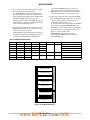
1
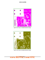
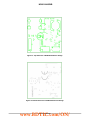
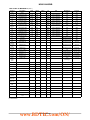
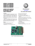
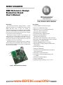
NCN51206GEVB KNX Reference Design Evaluation Board User'sManual http://onsemi.com EVAL BOARD USER’S MANUAL Introduction Key Features The NCN5120 Reference Design mimics a switch application suitable for use in KNX twisted pair networks (KNX TP1−256). Only 2 wires are needed for communication and power. It contains the NCN5120 KNX Transceiver which handles the transmission and reception of data on the bus. It will also generate all necessary voltages to power the board and external loads. The Reference Design contains a microcontroller with debug interface for custom firmware development. Up to 4 external switches can be monitored and up to 4 external loads can be controlled. A voltage between 3.3 V and 21 V is available to drive the external loads. The NCN5120 Reference Design assures safe coupling to and decoupling from the KNX bus. Bus monitoring warns the external microcontroller for loss of power so that critical data can be stored in time. 9,600 baud KNX Communication Speed Supervision of KNX Bus Voltage High Efficient 3.3 V to 21 V Selectable DC−DC Converter to Drive External Loads Monitoring of Power Regulators No Additional Power Supply Required Buffering of Sent Data Frames (Extended Frames Supported) Selectable UART or SPI Interface to Host Controller Selectable UART and SPI Baud Rate to Host Controller Optional CRC on UART to the Host Optional MARKER Character to the Host Optional Direct Coupling of RxD and TxD to Host (Analog Mode) Auto Polling (Optional) Temperature Monitoring Contains Freely Programmable Microcontroller for Custom Applications Monitoring of 4 External Switches Controlling of 4 External (High Voltage) Loads (e.g. LED’s) One Freely Usable Push Button 3 Freely Usable LED’s Operating Temperature Range −25C to +85C Figure 1. NCN5120 Reference Design www.BDTIC.com/ON/ Semiconductor Components Industries, LLC, 2013 May, 2013 − Rev. 3 1 Publication Order Number: EVBUM2169/D NCN51206GEVB BLOCK DIAGRAM RESETb, SAVEb NCN5120 MSP430 Interface UART or SPI Adj. Reg. 3 LED + Switch LED1,2,3, SW1 Figure 2. NCN5120 Reference Design Block Diagram CONNECTOR DESCRIPTION Table 1. CONNECTOR LIST AND DESCRIPTION Connector J1 and J2 Description KNX Bus Connection J3 External Switch Inputs and External Outputs J4 Microcontroller Debug Interface TYPICAL APPLICATION KNX Bus 4 Push Buttons (with each one blue LED) Figure 3. Typical Application www.BDTIC.com/ON/ http://onsemi.com 2 Connector J3 Clock ESD Protection 3.3 V Low Side Drive J1 and J2 Reverse Protection Diode + TVS Connector J4 NCN51206GEVB ELECTRICAL SPECIFICATION Recommend Operation Conditions Operating ranges define the limits for functional operation and parametric characteristics of the reference design. Note that the functionality of the reference design outside these operating ranges is not guaranteed. Operating outside the recommended operating ranges for extended periods of time may affect device reliability. Table 2. OPERATING RANGES Symbol Parameter Min Max Unit +20 +33 V 0 3.3 V 0 5 V 3.3 21 V +85 C VBUS Voltage on Positive Pin of J1 and J2 (Note 1) VDIG1 Input Voltage on J4 and J3 (Pins 1, 3, 5 and 7) VDIG2 Input Voltage on J3 (Pins 9, 11, 13 and 15) (Note 2) VDD2 Output Voltage on J3 (Pins 10, 12, 14 and 16) (Note 3) Ambient Temperature −25 Ta 1. Voltage indicates DC value. With equalization pulse bus voltage must be between 11 V and 45 V 2. Higher voltages are possible. See Adjustable DC−DC Converter page 13 for more details. 3. See Adjustable DC−DC Converter page 13 for the limitations! Table 3. DC PARAMETERS (The DC parameters are given for a reference design operating within the Recommended Operating Conditions unless otherwise specified.) Convention: currents flowing in the circuit are defined as positive. Symbol Connector Pin(s) Remark/Test Conditions Parameter Min Typ Max Unit Power Supply VBUS J1, J2 1 IBUS Bus DC Voltage Excluding Active and Equalization Pulse 20 − 33 V Bus Current Consumption Normal Operating Mode, No External Load, DC1 and DC2 Enabled, Continuous Transmission of ‘0’ on the KNX Bus by another KNX Device − 5 − mA − 18.0 − V VBUSH Undervoltage Release Level VBUS Rising (Figure 4) VBUSL Undervoltage Trigger Level VBUS_Hyst VBUS Falling (Figure 4) Undervoltage Hysteresis − 16.8 − V 0.6 − − V KNX Bus Coupler Icoupler_lim J1, J2 1 Bus Coupler Current Limitation R10 Not Mounted 13 − 30 mA R10 Mounted 26 − 60 mA Output Voltage VBUS > VDD2 3.3 − 21 V Undervoltage Release Level VDD2 Rising (Figure 5) − 0.9 VDD2 − V Undervoltage Trigger Level VDD2 Faling (Figure 5) − 0.8 VDD2 − V VDD2_rip Output Voltage Ripple VBUS = 26 V, VDD2 = 3.3 V, IDD2 = 40 mA − 40 − mV IDD2_lim Overcurrent Threshold −100 − −200 mA − 90 − % Adjustable DC−DC Converter VDD2 VDD2H VDD2L VDD2 J3 10, 12, 14, 16 Power Efficiency Vin = 26 V, VDD2 = 3.3 V, IDD2 = 35 mA www.BDTIC.com/ON/ http://onsemi.com 3 NCN51206GEVB Table 3. DC PARAMETERS (continued) (The DC parameters are given for a reference design operating within the Recommended Operating Conditions unless otherwise specified.) Convention: currents flowing in the circuit are defined as positive. Symbol Connector Pin(s) Remark/Test Conditions Parameter Min Typ Max Unit Logic Low Threshold 0 − 0.7 V Logic High Threshold 2.65 − 3.3 V Logic Low Output Level 0 − 0.6 V Logic High Output Level VDD1 − 0.6 − VDD1 V − − 0.4 V Digital Inputs VIL VIH J3 1, 3, 5, 7 J4 2, 3, 4, 5, 6, 8 J3 1, 3, 5, 7 J4 2, 3, 4, 5, 6, 8 Digital Ouputs VOL J4 VOH J4 VOL_OD J3 9, 11, 13, 15 Logic Low Level Open Drain IOL = 5 mA Table 4. AC PARAMETERS (The AC parameters are given for a reference design operating within the Recommended Operating Conditions unless otherwise specified.) Symbol Pin(s) Parameter Remark/Test Conditions Min Typ Max Unit (Figure 4) − 2 − ms SPI Baudrate Depending on Configuration Input Bits (see Interface Mode page 14). Tolerance is Equal to Xtal Oscillator Tolerance. (Figure 6) − 2 − ms − 8 − ms − tsck / 2 − Power Supply tBUS_FILTER VBUS1 VBUS1 Filter Time MASTER Serial Peripheral Interface (MASTER SPI) tsck SCK tSCK_HIGH SPI Clock High Time tSCK_LOW tSDI_SET SPI Clock Low Time SDI tSDI_HOLD tSDO_VALID SPI Clock Period SPI Data Input Setup Time SPI Data Input Hold Time SDO − tsck / 2 − 125 − − ns 125 − − ns − − 100 ns SPI Data Output Valid Time CL = 20 pF (Figure 6) tCS_HIGH SPI Chip Select High Time (Figure 6) 0.5 tSCK − − tCS_SET SPI Chip Select Setup Time 0.5 tSCK − − SPI Chip Select Hold Time 0.5 tSCK − − CSB tCS_HOLD (Figure 6) tTREQ_LOW TREQ Low Time 125 − − ns tTREQ_HIGH TREQ High Time 125 − − ns TREQ Setup Time 125 − − ns TREQ Hold Time 125 − − ns − 19,200 − Baud − 38,400 − Baud tTREQ_SET TREQ tTREQ_HOLD Universal Asynchronous Receiver/Transmitter (UART) fUART TXD, RXD UART Interface Baudrate Baudrate Depending on Configuration Input Pins (see Interface Mode page 14). Tolerance is equal to tolerance of Xtal oscillator tolerance. www.BDTIC.com/ON/ http://onsemi.com 4 NCN51206GEVB VBUS VBUSH VBUSL t BUS_FILTER t BUS_FILTER t <VBUS> Comments: <VBUS> is an internal signal which can be verified with the Internal State Service . Figure 4. Bus Voltage Undervoltage Threshold VDD2 VDD2H VDD2L t <VDD2> Comments: <VDD2> is an internal signal which can be verified with the System State Service. Figure 5. VDD2 Undervoltage Threshold CS CLK ÎÎÎÎÎÎ ÎÎÎÎÎÎ ÎÎÎÎÎÎ ÎÎÎÎÎÎ DI DO tSDI_SET tCS _SET ÎÎÎÎÎÎÎÎÎÎÎÎÎÎÎÎ ÎÎÎÎÎÎÎÎÎÎÎÎÎÎÎÎ ÎÎÎÎÎÎÎÎÎÎÎÎÎÎ ÎÎÎÎÎÎÎÎÎÎÎÎÎÎ tSDI _HOLD tCS _HIGH t SDO_VALID tSCK _HIGH tSCK _LOW tSCK tCS_HOLD Figure 6. SPI Bus Timing Diagram www.BDTIC.com/ON/ http://onsemi.com 5 NCN51206GEVB THyst T THyst TTSD DT TTW t <TW> SAVEB Normal Stand−By Start−Up Reset Stand−By Normal RESETB Analog State Comments : −<TW> is an internal signal which can be verified with the System State Service. −No SPI / UART communication possible when RESETB is low! −It’s assumed all voltage supplies are within their operating condition. Figure 7. Temperature Monitoring Levels CS CLK ÎÎÎÎÎ ÎÎÎÎÎ ÎÎÎÎÎ ÎÎÎÎÎ DI DO LSB 1 Dummy 2 Dummy 7 Dummy ÎÎÎÎÎÎÎÎÎ ÎÎÎÎÎÎÎÎÎ ÎÎÎÎÎÎÎÎ ÎÎÎÎÎÎÎÎ Dummy TREQ tTREQ _SET tTREQ_HOLD tTREQ _LOW tTREQ_HIGH Figure 8. TREQ Timing Diagram www.BDTIC.com/ON/ http://onsemi.com 6 NCN51206GEVB APPLICATION SCHEMATIC Figure 9. Schematic of NCN5120 Reference Design (Part 1) www.BDTIC.com/ON/ http://onsemi.com 7 NCN51206GEVB APPLICATION SCHEMATIC Figure 10. Schematic of NCN5120 Reference Design (Part 2) www.BDTIC.com/ON/ http://onsemi.com 8 NCN51206GEVB Figure 11. Top Layer of NCN5120 Reference Design Figure 12. Bottom Layer of NCN5120 Reference Design www.BDTIC.com/ON/ http://onsemi.com 9 NCN51206GEVB Figure 13. Inner Layer 1 of NCN5120 Reference Design Figure 14. Inner Layer 2 of NCN5120 Reference Design www.BDTIC.com/ON/ http://onsemi.com 10 NCN51206GEVB Figure 15. Top Silkscreen of NCN5120 Reference Design Figure 16. Bottom Silkscreen of NCN5120 Reference Design www.BDTIC.com/ON/ http://onsemi.com 11 NCN51206GEVB Table 5. BILL OF MATERIALS (Note 1) Reference Part Number Value Voltage Power Tol Type Manufacturer Footprint CON1 243-211 Wago NA C1, C2 C1005COG1H100D 10 pF 6.3V 5% Ceramic Multilayer TDK 0402 C3, C4, C7 C1005X5R0J104M 100 nF 6.3V 20% Ceramic Multilayer TDK 0402 C5 C1608X7R1H473M 47 nF 50V 20% Ceramic Multilayer TDK 0603 C6 C1005X5R1H472K 4.7 nF 50V 10% Ceramic Multilayer TDK 0402 C8 B41145A7107M000 100 mF 35V 20% Aluminum Electrolytic Epcos 8 10 C10 (Note 2) C1005COG1H100D 10 pF 6.3V 5% Ceramic Multilayer TDK 0402 C11 C2012X5R1E106M 10 mF 25V 20% Ceramic Multilayer TDK 0805 C12 C1608X5R0J106M 10 mF 6.3V 20% Ceramic Multilayer TDK 0603 C13 C1608X5R1H105M 1 mF 50V 20% Ceramic Multilayer TDK 0603 C15, C16 C1005X5R0J105M 1 mF 6.3V 20% Ceramic Multilayer TDK 0402 C17 C1005C0G1H120J 12 pF 6,3V 5% Ceramic Multilayer TDK 0402 SMA D1 SS16T3G ON Semiconductor D2 1SMA40AT3G ON Semiconductor SMA D3 (Note 2) NSR0520V2T1G ON Semiconductor SOD-523 D5, D6, D7, D8 ESD5Z3.3T1G ON Semiconductor SOD-523 D14, D15 SMF05CT1G ON Semiconductor SOT-363-6 J1, J2 RT−01T−1.0B(LF) JST 5.75 mm pitch J3 622 016 211 21 Wurth Elektronik 1,27 mm pitch J4 620 008 211 21 Wurth Elektronik 2 mm pitch L1, L2 DA54NP−221K Coils Electronic See Datasheet LED1, LED2, LED3 HSMG−C190 Avago Technologies 1.6 0.8 220 mH 10% Q1, Q2 NTJD4001NT1G ON Semiconductor SOT-363-6 R4 RC1218JK−xx22RL 22 W 1W 10% Thick Film Yageo 1218 R5 RC0402JR−xx0RL 0W 0.0625 W NA Thick Film Yageo 0402 R6 RC0402JR−xx33KL 33 kW 0.0625 W 5% Thick Film Yageo 0402 R7, R8 RC0402JR−xx1RL 1W 0.0625 W 5% Thick Film Yageo 0402 R9 RC0402JR−xx180KL 180 kW 0.0625 W 5% Thick Film Yageo 0402 R10 (Note 2) RC0402JR−xx0RL 0W 0.0625 W NA Thick Film Yageo 0402 R15, R18, R23, R26 RC0402JR−xx1KL 1 kW 0.0625 W 5% Thick Film Yageo 0402 R16, R19, R24, R27 RC0402JR−xx1ML 1 MW 0.0625 W 5% Thick Film Yageo 0402 R20, R28, R29 RC0402JR−xx1KL 1 kW 0.0625 W 5% Thick Film Yageo 0402 R21 RC0402JR−xx100KL 100 kW 0.0625 W 5% Thick Film Yageo 0402 SW1 434 123 025 816 Wurth Elektronik See Datasheet U1 NCN5120 ON Semiconductor QFN-40 U2 MSP430F2370IRHAx Texas Instruments VQFN-40 Y1 FA-238, 16 MHz, 50 ppm, 10 pF Epson Toyocom 3.2 2.5 1. All devices are Pb-Free. 2. Not mounted. www.BDTIC.com/ON/ http://onsemi.com 12 NCN51206GEVB FUNCTIONAL DESCRIPTION Because the NCN5120 Reference Design contains the NCN5120 KNX Transceiver (KNX Certified) no details on KNX will be given in this document. Detailed information on the Certified KNX Transceiver NCN5120 can be found in the NCN5120 datasheet (www.onsemi.com). Detailed information on the KNX Bus can be found on the KNX website and in the KNX standards (www.knx.org). the KNX standard. Minimum VBUS is 20 V (see KNX standard). Above formula gives only an estimation and will mainly depend on the firmware loaded on the microcontroller (U2, see Figure 10). One must always verify that the KNX bus loading is in line with the KNX Specification under all operating conditions! KNX Bus Connection Xtal Oscillator Connection to the KNX bus is done by means of J1 or J2. A standard Wago connector (type 243−211) can be used for this (see Figure 17). A reverse protection diode (D1, Figure 10) is foreseen (mandatory) as also a Transient Voltage Suppressor (D2, Figure 10). A crystal of 16 MHz (Y1, see Figure 10) is foreseen on the reference design. This clock signal is also supplied to the microcontroller. See the NCN5120 datasheet (www.onsemi.com) for more details on this signal. RESETB and SAVEB The KNX transceiver NCN5120 controls the reset state of the microcontroller by means of the RESETB signal. An additional signal SAVEB can be monitored by the microcontroller to detect possible issues. See NCN5120 datasheet for more details on these two signals. Voltage Supervisors NCN5120 has different voltage supervisors. Please check the NCN5120 datasheet for more details. Temperature Monitor Figure 17. KNX Bus Connector NCN5120 produces an over-temperature warning (TW) and a thermal shutdown warning (TSD). Please check the NCN5120 datasheet for more details. The KNX bus can be connected to J1 if the break-out section is removed from the PCB. When removed the KNX Bus connector (Figure 17) will fit nicely inside the PCB. External IO The reference design has the possibility to monitor up to 4 inputs (pin 1, 3, 5 and 7 of J3) and control up to 4 outputs (pin 9, 11, 13 and 15 of J3). The input pins are 3.3 V compliant and ESD protected (D5 D8, Figure 10). J3 is connected in such a way that an easy connection between the input and ground is possible. The microcontroller (U2, see Figure 10) should be configured with an internal pull-up (see microcontroller datasheet on how to do this). The external outputs are driven by means of low-side drivers (Q1 and Q2, see Figure 10). A gate resistor is foreseen for slope control (R15, R18, R23 and R26 of Figure 10). J3 is routed in such a way that the load can easily be connected between the output (low-side driver) and VDD2. Q1 and Q2 can be used over the complete VDD2 voltage range. ESD diodes D14 and D15 need to be replaced if VDD2 is increased (see also Adjustable DC-DC Converter). Adjustable DC−DC Converter NCN5120 provides the power for the complete reference design. It has also a second power supply which can be used to drive external loads. The voltage is programmable between 3.3V and 21V by means of an external resistor divider (R6 and R9, see Figure 10). The voltage divider can be calculated as next: R6 + R 9 R VDD2M R 9 ) R VDD2M V DD2 * 3.3 3.3 (eq. 1) RVDD2M is between 60 kW and 140 kW (typical 100 kW). The DC value of the KNX bus should at least be higher than VDD2. Be aware that when changing the VDD2 voltage, D14 and D15 (see Figure 10) need to be replaced. Check the SMF05C datasheet for possible replacements (www.onsemi.com). Although VDD2 is capable of delivering 100 mA, the maximum current capability will not always be usable. One needs to make sure that the KNX bus power consumption stays within the KNX specification. The maximum allowed current for VDD2 can be calculated as next: V BUS I BUS w 2 ƪ0.033 ) ǒV DD2 I DD2Ǔƫ Push Button and LED’s One push button (SW1) and 3 LED’s (LED1 LED3) are foreseen on the reference design. These are freely usable. (eq. 2) Microcontroller Debug Interface J4 is the microcontroller debug interface. See the microcontroller datasheet for more info on how to use this interface. IBUS is limited by NCN5120. If R10 is not mounted, IBUS can maximum be 13 mA. If R10 is mounted, IBUS can maximum be 26 mA. IBUS will however also be limited by www.BDTIC.com/ON/ http://onsemi.com 13 NCN51206GEVB Interface Mode of NCN5120. It is not allowed to use the reference design in a final product or to sell it as a KNX Certified product. Contact ON Semiconductor if you want to use the reference design as a final product. The device can communicate with the host controller by means of a UART interface or an SPI interface. The selection of the interface is done by the pins MODE1, MODE2, TREQ, SCK/UC2 and CSB/UC1 which are connected to the microcontroller (see Figure 10). More details on the different interfaces can be found back in Table 6 and the NCN5120 datasheet. 2. What 3rd party companies do you recommend for the higher layer stacks? ON Semiconductor does not recommend any 3rd party company in particular. Several 3rd party companies have KNX Certified stacks and it’s always advised to use one of these stacks. Some companies have experience with NCN5120. Contact ON Semiconductor for more information. Digital Description The implementation of the Data Link Layer as specified in the KNX standard is divided in two parts. All functions related to communication with the Physical Layer and most of the Data Link Layer services are inside NCN5120, the rest of the functions and the upper communication layers are implemented into the microcontroller (see Figure 10 and Figure 18). The host controller is responsible for handling: Checksum Parity Addressing Length 3. Can we freely reuse the schematic and layout of this reference design? It is allowed to reuse the schematic, components and layout of the NCN5120 reference design for your own application. Because the operating conditions of your design are not known by ON Semiconductor, one must always fully verify the design even if it’s based on this reference design. Contact ON Semiconductor if additional information is required. The NCN5120 is responsible for handling: Checksum Parity Acknowledge Repetition Timing 4. Can we request ON Semiconductor to supply the higher layer stacks? By no means will ON Semiconductor provide any higher layer stacks. Certified higher layer stacks can be provided by 3rd party companies (see also Firmware). Services All services can be found back in the NCN5120 datasheet (www.onsemi.com). 5. How much load can the outputs drive? The maximum allow load can be calculated with the formula as given in Adjustable DC-DC Converter (page x13). IDD2 defines the maximum load the outputs can drive in total. Firmware No special firmware is provided with the reference design. There will be some basic firmware flashed on the microcontroller (U2, Figure 10) but this is only used to verify the reference design before shipment. The user has the possibility to develop his own firmware but help on programming the microcontroller will not be provided my ON Semiconductor. NCN5120 contains the physical layer and a part of the data link layer (see Figure 18). ON Semiconductor can provide a library for the microcontroller to complete the data link layer. By no means will ON Semiconductor provide any of the higher layer stacks (Network Layer, Transport Layer, ). Sufficient 3rd party companies are available which have certified higher layer stacks. 6. What is the usage of ARXD and ATXD (Figure 10)? These pins have no meaning and cannot be used. 7. I’ve tried all possible R6 and R9 combinations but I’m not capable of setting VDD2 above 6 V. How does this come? As can be seen in Figure 10, VDD2 (5 V) is connected to an ESD protection diode (D14). This is a 5 V ESD protection diode. Whenever one tries to set VDD2 above 5 V, this ESD diode will trigger and limit the VDD2 voltage to about 6 V. This issue can be solved by, or removing D14 (in an ESD safe area this should not be an issue), or by replacing this 5 V ESD diode with a higher voltage version (see the ESD5Z datasheet for other versions (www.onsemi.com)). FAQs 1. Is this reference design KNX Certified? No, only NCN5120 is KNX Certified. The reference design may only be used for evaluation www.BDTIC.com/ON/ http://onsemi.com 14 NCN51206GEVB wires on the KNX REV6 board. It is however advised to remove the microcontroller from the KNX REV6 board or to put the microcontroller in reset (short pins 8 and 7 of J4 (see Figure 10)). 8. Is it possible to test all possible interfaces (UART, SPI, Analog Mode) with KNX REV6? Yes, the KNX REV6 board can be used with all possible interfaces. One has to be careful however when using the Analog Mode. In the Analog Mode the digital of NCN5120 is bypassed. If the microcontroller would force the RXD−pin (pin 29) of NCN5120 low, NCN5120 would pull the KNX bus low which could lead to issues. 10. I’m trying to sink more than 13 mA from the KNX bus with KNX REV6 but I’m having issues with the voltage regulators whenever I’m going above 16 mA. What could be the issue? To be able to take more than 13 mA from the KNX bus one needs to pull the FANIN/WAKE−pin of NCN5120 low. This can be done by mounting R10 (zero Ohm resistor). After mounting of R10 (see Figure 9), verify carefully if the FANIN/WAKE−pin is pulled to ground! See NCN5120 datasheet for more info on the FANIN/WAKE−pin. 9. Is it possible to bypass the microcontroller on the KNX REV6 board and connect NCN5120 directly with our microcontroller board? Although the board is not designed for this, this is possible. One could connect NCN5120 directly to your microcontroller board by soldering some Table 6. INTERFACE SELECTION TREQ MODE2 MODE1 SCK/UC2 SCB/UC1 SDI/RXD SDO/TXD Description 0 0 0 0 0 RXD TXD 9-bit UART-Mode, 19,200 bps 0 0 0 0 1 9-bit UART-Mode, 38,400 bps 0 0 0 1 0 8-bit UART-Mode, 19,200 bps 0 0 0 1 1 8-bit UART-Mode, 38,400 bps 1 0 0 X X Driver Receiver Analog Mode TREQ 0 1 SCK (out) CSB (out) SDI SDO SPI Master, 125 kbps TREQ 1 0 SPI Master, 500 kbps 7 Application Layer 6 Presentation Layer 5 Session Layer 4 Transport Layer 3 Network Layer Host Controller NOTE: X = Don’t Care Logic Link Control Data Link Layer Media Access Control 1 Physical Layer NCN5120 2 Figure 18. OSI Model Reference www.BDTIC.com/ON/ http://onsemi.com 15 NCN51206GEVB BOARD DIMENSIONS 30 .0 11 .3 9.5 1.9 2.1 18.5 21.3 27.1 30.0 1.5 2.7 12.4 − Above dimensions are in mm −Height C8 = 11 mm − Height J 3 = 5.3 mm − Height J 4 = 6 mm −Height L1 and L2 (bottom side of PCB ) = 4.8 mm The product described herein may be covered by one or more US patents pending. ON Semiconductor and are registered trademarks of Semiconductor Components Industries, LLC (SCILLC). SCILLC owns the rights to a number of patents, trademarks, copyrights, trade secrets, and other intellectual property. A listing of SCILLC’s product/patent coverage may be accessed at www.onsemi.com/site/pdf/Patent−Marking.pdf. SCILLC reserves the right to make changes without further notice to any products herein. SCILLC makes no warranty, representation or guarantee regarding the suitability of its products for any particular purpose, nor does SCILLC assume any liability arising out of the application or use of any product or circuit, and specifically disclaims any and all liability, including without limitation special, consequential or incidental damages. “Typical” parameters which may be provided in SCILLC data sheets and/or specifications can and do vary in different applications and actual performance may vary over time. All operating parameters, including “Typicals” must be validated for each customer application by customer’s technical experts. SCILLC does not convey any license under its patent rights nor the rights of others. SCILLC products are not designed, intended, or authorized for use as components in systems intended for surgical implant into the body, or other applications intended to support or sustain life, or for any other application in which the failure of the SCILLC product could create a situation where personal injury or death may occur. Should Buyer purchase or use SCILLC products for any such unintended or unauthorized application, Buyer shall indemnify and hold SCILLC and its officers, employees, subsidiaries, affiliates, and distributors harmless against all claims, costs, damages, and expenses, and reasonable attorney fees arising out of, directly or indirectly, any claim of personal injury or death associated with such unintended or unauthorized use, even if such claim alleges that SCILLC was negligent regarding the design or manufacture of the part. SCILLC is an Equal Opportunity/Affirmative Action Employer. This literature is subject to all applicable copyright laws and is not for resale in any manner. PUBLICATION ORDERING INFORMATION LITERATURE FULFILLMENT: Literature Distribution Center for ON Semiconductor P.O. Box 5163, Denver, Colorado 80217 USA Phone: 303−675−2175 or 800−344−3860 Toll Free USA/Canada Fax: 303−675−2176 or 800−344−3867 Toll Free USA/Canada Email: [email protected] N. American Technical Support: 800−282−9855 Toll Free USA/Canada Europe, Middle East and Africa Technical Support: Phone: 421 33 790 2910 Japan Customer Focus Center Phone: 81−3−5817−1050 ON Semiconductor Website: www.onsemi.com Order Literature: http://www.onsemi.com/orderlit For additional information, please contact your local Sales Representative www.BDTIC.com/ON/ http://onsemi.com 16 EVBUM2169/D