1
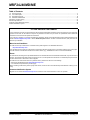
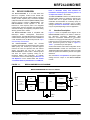
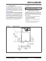
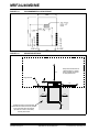
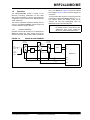
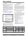
MRF24J40MD/ME 2.4 GHz IEEE Std. 802.15.4™ RF Transceiver Module with PA/LNA Features: Operational: • IEEE Std. 802.15.4™ Compliant RF Transceiver • Supports ZigBee®, MiWi™ Development Environment Proprietary Wireless Networking Protocols • 4-Wire Serial Peripheral Interface (SPI) with Interrupt • Small size: 0.9" x 1.3" (22.9 mm x 33.0 mm), Surface Mountable: Pin Compatible with MRF24J40MB and MRF24J40MC • Integrated Crystal, Internal Voltage Regulator, Matching Circuitry, Power Amplifier, Low Noise Amplifier • PCB Antenna (MRF24J40MD), External Antenna Connector (MRF24J40ME): Ultra Miniature Coaxial (U.FL), 50Ω • Easy Integration into Final Product: Minimize Product Development, Quicker Time to Market • Compliance: - Modular Certified for the United States (FCC) and Canada (IC) - European R&TTE Directive Assessed Radio Module - Australia/New Zealand • Compatible with Microchip microcontroller families (PIC16, PIC18, PIC24, dsPIC33 and PIC32) • Range up to 4000 ft • Operating Voltage: 3.0V-3.6V (3.3V typical) • Temperature Range: -40°C to +85°C Industrial • Low-Current Consumption: - Rx Mode: 32 mA (typical) - Tx Mode: 140 mA (typical) - Sleep: 10 A (typical) RF/Analog Features: • ISM Band 2.405 GHz-2.475 GHz Operation • Data Rate: 250 kbps • -104 dBm Typical Sensitivity with -23 dBm Maximum Input Level • +19 dBm Typical Output Power with 45 dB Tx Power Control Range • Integrated Low Phase Noise VCO, Frequency Synthesizer and PLL Loop Filter • Digital VCO and Filter Calibration • Integrated RSSI ADC and I/Q DACs • Integrated LDO • High Receiver RSSI Dynamic Range MAC/Baseband Features: • Hardware CSMA-CA Mechanism, Automatic ACK Response and FCS Check • Independent Beacon, Transmit and GTS FIFO • Supports all CCA modes and RSS/LQI • Automatic Packet Retransmit Capable • Hardware Security Engine (AES-128) with CTR, CCM and CBC-MAC modes • Supports Encryption and Decryption for MAC Sub layer and Upper Layer Pin Diagram: GND RESET WAKE INT SDI SCK 2014 Microchip Technology Inc. 1 2 3 4 5 6 12 11 10 9 8 7 Advance Information GND GND VIN NC CS SDO DS70005173A-page 1 MRF24J40MD/ME Table of Contents 1.0 Device Overview .......................................................................................................................................................................... 3 2.0 Circuit Description ...................................................................................................................................................................... 11 3.0 Regulatory Approval................................................................................................................................................................... 19 4.0 Electrical Characteristics ........................................................................................................................................................... 25 Appendix A: Revision History............................................................................................................................................................... 27 The Microchip Web Site ....................................................................................................................................................................... 29 Customer Change Notification Service ................................................................................................................................................ 29 Product Identification System............................................................................................................................................................... 30 TO OUR VALUED CUSTOMERS It is our intention to provide our valued customers with the best documentation possible to ensure successful use of your Microchip products. To this end, we will continue to improve our publications to better suit your needs. Our publications will be refined and enhanced as new volumes and updates are introduced. If you have any questions or comments regarding this publication, please contact the Marketing Communications Department via E-mail at [email protected] or fax the Reader Response Form in the back of this data sheet to (480) 792-4150. We welcome your feedback. Most Current Data Sheet To obtain the most up-to-date version of this data sheet, please register at our Worldwide Web site at: http://www.microchip.com You can determine the version of a data sheet by examining its literature number found on the bottom outside corner of any page. The last character of the literature number is the version number, (e.g., DS30000A is version A of document DS30000). Errata An errata sheet, describing minor operational differences from the data sheet and recommended workarounds, may exist for current devices. As device/documentation issues become known to us, we will publish an errata sheet. The errata will specify the revision of silicon and revision of document to which it applies. To determine if an errata sheet exists for a particular device, please check with one of the following: • Microchip’s Worldwide Web site; http://www.microchip.com • Your local Microchip sales office (see last page) When contacting a sales office, please specify which device, revision of silicon and data sheet (include literature number) you are using. Customer Notification System Register on our web site at www.microchip.com to receive the most current information on all of our products. DS70005173A-page 2 Advance Information 2014 Microchip Technology Inc. MRF24J40MD/ME 1.0 DEVICE OVERVIEW The MRF24J40MD/ME is a 2.4 GHz IEEE Std. 802.15.4™ compliant, surface mount module with integrated crystal, internal voltage regulator, matching circuitry, Power Amplifier (PA), Low Noise Amplifier (LNA) with PCB Trace Antenna (MRF24J40MD) or 50Ω external antenna connector (MRF24J40ME). The MRF24J40MD/ME module operates in the nonlicensed 2.4 GHz frequency band. The integrated module design frees the integrator from extensive RF and antenna design, and regulatory compliance testing allowing quicker time to market. The MRF24J40MD/ME module is compatible with Microchip’s MiWi™ Development Environment software stacks. The MiWi Development Environment software stack including the source code is available as a free download, from the Microchip web site: http:// www.microchip.com/wireless. The MRF24J40MD/ME module has received regulatory approvals for modular devices in the United States (FCC) and Canada (IC). Modular approval removes the need for expensive RF and antenna design, and allows the end user to place the MRF24J40MD/ME module inside a finished product and does not require regulatory testing for an intentional radiator (RF transmitter). To maintain conformance, refer to module settings in Section 3.1.2 “RF Exposure” for the United States and Section “Transmitter Antenna (from Section 7.1.2 RSS-Gen, FIGURE 1-1: Issue 3, December 2010): User manuals for transmitters shall display the following notice in a conspicuous location:” for Canada. The MRF24J40MD/ME module is an R&TTE Directive assessed radio module for operation in Europe. The module tests can be applied toward final product certification and Declaration of Conformity (DoC). To maintain conformance for Europe, refer to module settings in Section 3.4 “Australia”. Additional testing may be required depending on the end application. 1.1 Interface Description Figure 1-1 shows a simplified block diagram of the MRF24J40MD/ME module. The module is based on the Microchip Technology MRF24J40 IEEE 802.15.4™ 2.4 GHz RF Transceiver IC. The module interfaces to many popular Microchip PIC® microcontrollers through a 4-wire SPI interface, interrupt, wake, reset, power and ground, as shown in Figure 1-2. Table 1-1 provides the pin descriptions. Serial communication and module configuration for the MRF24J40MD/ME module are documented in the “MRF24J40 Data Sheet” (DS39776). Refer to the data sheet for specific serial interface protocol and register definitions. Also, see Section 1.4 “Operation” for specific register settings that are unique to the MRF24J40MD/ME module. MRF24J40MD/ME BLOCK DIAGRAM MRF24J40MD/ME IEEE Std. 802.15.4™ Module MRF24J40 PA Antenna U.FL Connector Interface Physical SPI Digital I/O MAC Power Management LNA Power 20 MHz Crystal 2014 Microchip Technology Inc. Advance Information DS70005173A-page 3 MRF24J40MD/ME TABLE 1-1: PIN DESCRIPTION Pin Symbol Type Description 1 GND Ground 2 RESET DI Global hardware Reset pin 3 WAKE DI External wake-up trigger 4 INT DO Interrupt pin to microcontroller 5 SDI DI Serial interface data input 6 SCK DI Serial interface clock 7 SDO DO Serial interface data output from MRF24J40 8 CS DI Serial interface enable 9 NC — No connection Ground 10 VIN Power Power supply 11 GND Ground Ground 12 GND Ground Ground Legend: Pin type abbreviation: D = Digital, I = Input, O = Output FIGURE 1-2: MICROCONTROLLER TO MRF24J40MD/ME INTERFACE PIC® MCU DS70005173A-page 4 MRF24J40MD/ME I/O CS SDO SDI SDI SDO SCK SCK INTX INT VIN GND I/O WAKE I/O RESET Advance Information 2014 Microchip Technology Inc. MRF24J40MD/ME 1.2 Mounting Details The MRF24J40MD/ME is a surface mountable module. Module dimensions are shown in Figure 1-3. The module Printed Circuit Board (PCB) is 0.032" thick with castellated mounting points on the edge. Figure 1-4 is a recommended host PCB footprint for the MRF24J40MD/ME. The MRF24J40MD has an integrated PCB antenna. For the best performance, follow the mounting details shown in Figure 1-5. It is recommended that the module be mounted on the edge of the host PCB, and an area around the antenna, approximately 1.2", be kept clear of metal objects. A host PCB ground plane around the MRF24J40MD acts as a counterpoise to the PCB antenna. It is recommended to extend the ground plane at least 0.4" around the module. FIGURE 1-3: The MRF24J40ME has 50Ω ultra miniature coaxial (U.FL) connector. Caution: The U.FL connector is fragile and can only tolerate very limited number of insertions. 1.3 Soldering Recommendations The MRF24J40MD/ME module was assembled using a standard lead-free reflow profile. The module is compatible with standard lead-free solder reflow profiles. To avoid damaging the module, the following recommendations are given: • Refer to the solder paste data sheet for specific reflow profile recommendations • Use no-clean flux solder paste • Do not wash as moisture can be trapped under the shield • Use only one flow. If the PCB requires multiple flows, apply the module on the last flow MODULE DETAILS 2014 Microchip Technology Inc. Advance Information DS70005173A-page 5 MRF24J40MD/ME FIGURE 1-4: RECOMMENDED PCB FOOTPRINT FIGURE 1-5: MOUNTING DETAILS 1.2” Keep area around antenna (approximately 1.2 inches) clear of metallic structures for best performance Edge of PCB 1.2” 0.315” 0.4” PCB Ground Plane (Counterpoise) Underneath and extend as far as possible to the sides and below the module (at least 0.4 inches on each side) for best performance DS70005173A-page 6 0.4” 0.4” Advance Information 2014 Microchip Technology Inc. MRF24J40MD/ME 1.4 Operation The MRF24J40MD/ME module is based on the Microchip Technology MRF24J40 2.4 GHz IEEE 802.15.4 RF Transceiver IC. Serial communication and configuration are documented in the “MRF24J40 Data Sheet” (DS39776). This section emphasizes operational settings that are unique to the MRF24J40MD/ME module design that must be followed for proper operation. 1.4.1 pins on the MRF24J40. Figure 1-6 shows the PA/LNA block diagram. Figure 2-5 is the schematic diagram for the module. The internal RF state machine is configured for the PA/ LNA Mode by setting TESTMODE (0x22<2:0>) = 111. Pins GPIO0, GPIO1 and GPIO2 control the RF switches, PA and LNA automatically when the MRF24J40 receives and transmits data. Note: A complete explanation of the operation of the PA/LNA control is documented in the “MRF24J40 Data Sheet” (DS39776), Section 4.2 “External PA/LNA Control”. PA/LNA CONTROL Operation of the PA U6 and LNA U1 is controlled by the MRF24J40 internal RF state machine through RF switches, U3 and U4, and the GPIO0, GPIO1 and GPIO2 FIGURE 1-6: PA/LNA BLOCK DIAGRAM RF Switch RF3023TR7 LNA SST12LN01 RF Switch RF3023TR7 LNA U.FL Connector (ME) Balun BPF V2 V1 PCB Antenna (MD) PA PA SST12LP17E RFN V2 V1 MRF24J40 TX RX PA_ON 2014 Microchip Technology Inc. RFP Advance Information GPIO1 GPIO2 GPIO0 DS70005173A-page 7 MRF24J40MD/ME 1.4.2 ENERGY DETECTION (ED) 1.4.3 SLEEP Before performing an energy detection (see Section 3.6.1 “RSSI Firmware Request (RSSI Mode 1)” in the “MRF24J40 Data Sheet” (DS39776), perform the following steps: To get the lowest power consumption from the MRF24J40MD/ME module during Sleep, it is necessary to disable the PA, PA voltage regulator and LNA. To do this, perform the following steps: 1. 1. 2. 3. 4. Configure the internal RF state machine to normal operation (TESTMODE (0x22F<2:0>) = 000). Configure GPIO2 and GPIO1 direction for output (TRISGP2 (0x34<2>) = 1 and TRISGP1 (0x34<1>) = 1). Set GPIO2 (0x33<2>) = 1 and GPIO1 (0x32<1>) = 0. This enables the LNA and disables the PA. Perform the energy detection following the steps in Section 3.6.1 “RSSI Firmware Request (RSSI Mode 1)” in the “MRF24J40 Data Sheet” (DS39776). Note: 2. 3. 4. Configure the internal RF state machine to normal operation (TESTMODE (0x22F<2:0>) = 000). Configure the GPIO2, GPIO1 and GPIO0 direction for output (TRISGP2 (0x34<2>) = 1, TRISGP1 (0x34<1>) = 1) = 1 and TRISGP0 (0x34<0>) = 1). Set GPIO2 (0x33<2>) = 0 and GPIO1 (0x32<1>) = 0. This disables the LNA and the PA. Put the MRF24J40 to Sleep following the steps in the “MRF24J40 Data Sheet” (DS39776). When waking the module, re-enable the PA/LNA Mode. The LNA will amplify the received signal. The RSSI value will include the receive signal strength plus the LNA amplification. DS70005173A-page 8 Advance Information 2014 Microchip Technology Inc. MRF24J40MD/ME 1.4.4 TRANSMIT POWER SETTINGS Table 1-2 lists the power settings in register RFCON3 (0x203<7:3>) and the output power at antenna connector J1. TABLE 1-2: MRF24J40ME TRANSMIT POWER SETTINGS RFCON3 (0x203<7:3>) MRF24J40 Power Setting Conducted Output Power(1) (dBm) 11111 –36.3 -13.6 11110 –34.9 -12.4 11101 –33.7 -11.5 11100 –32.8 -10.7 11011 –31.9 -10.0 11010 –31.2 -9.6 11001 –30.5 -9.2 11000 –30.0 -3.4 10111 –26.3 -1.3 10110 –24.9 -0.7 10101 –23.7 0.1 10100 –22.8 0.5 10011 –21.9 1.0 10010 –21.2 1.3 10001 –20.5 5.8 10000 –20.0 7.0 01111 –16.3 8.1 01110 –14.9 9.0 01101 –13.7 9.7 01100 –12.8 10.4 01011 –11.9 10.9 01010 –11.2 11.3 01001 –10.5 16.0 01000 –10.0 17.2 00111 –6.3 17.9 00110 –4.9 18.5 Note 1: Note: 00101 –3.7 Typical output power at antenna connector J1, Channel 11, 50Ω impedance. 19.0 Refer to Section 3.0 “Regulatory Approval” for the required maximum power setting necessary to maintain certification requirements for each country the module will be used. 2014 Microchip Technology Inc. Advance Information DS70005173A-page 9 MRF24J40MD/ME NOTES: DS70005173A-page 10 Advance Information 2014 Microchip Technology Inc. MRF24J40MD/ME 2.0 CIRCUIT DESCRIPTION 2.1 The MRF24J40MD/ME is a 2.4 GHz IEEE Std. 802.15.4™ compliant surface mount module with integrated crystal, internal voltage regulator, matching circuitry, power amplifier, low noise amplifier with PCB trace antenna (MRF24J40MD) and 50Ω external antenna connector (MRF24J40ME). The MRF24J40MD/ME module interfaces to many popular Microchip PIC microcontrollers through a 4-wire SPI Interface, interrupt, wake, reset, power and ground. An example application schematic is illustrated in Figure 2-4. Serial communications and register definitions for the MRF24J40MD/ME module are documented in the “MRF24J40 Data Sheet” (DS39776). Refer to this data sheet for specific serial interface protocol and register definitions. Also, see Section 1.4 “Operation” for specific register settings that are unique to the MRF24J40MD/ME module. FIGURE 2-1: PCB Antenna (MRF24J40MD) The Printed Circuit Board (PCB) antenna is fabricated on the top copper trace of the module PCB. The layers below the antenna have no copper traces. The ground and power planes under the components serve as a counterpoise to the PCB antenna. Additional ground plane on the host PCB will substantially enhance the performance of the module. For best performance, place the module on the host PCB following the recommendations in Section 1.2 “Mounting Details”. The PCB antenna was designed and simulated using Ansoft Designer® and HFSS™ 3D full-wave solver software by Ansoft Corporation (www.ansoft.com) and tested in an anechoic room. The design goal was to create a compact, low-cost antenna with the best radiation pattern. Figure 2-1 shows the simulation drawing and Figure 2-2 and Figure 2-3 show the 2D and 3D radiation patterns, respectively. As shown by the radiation patterns, the performance of the antenna is dependent upon the orientation of the module. The discrete matching circuitry matches the impedance of the antenna with the MRF24J40 transceiver IC. PCB ANTENNA SIMULATION DRAWING 2014 Microchip Technology Inc. Advance Information DS70005173A-page 11 MRF24J40MD/ME FIGURE 2-2: SIMULATED 2D RADIATION PATTERN FIGURE 2-3: SIMULATED 3D RADIATION PATTERN 2.2 External Antenna (MRF24J40ME) The MRF24J40ME module has a 50Ω ultra miniature coaxial (U.FL) connector to connect to an external 2.4 GHz antenna. Caution: The U.FL connector is fragile and can only tolerate very limited number of insertions. TABLE 2-1: Type Whip Dipole Note 1: Modular certification of the MRF24J40ME module was performed with the external antenna types listed in Table 2-1. An antenna type comprises antennas having similar in-band and out-of-band radiation patterns. Refer to Section 3.0 “Regulatory Approval” for specific regulatory requirements by country. DS70005173A-page 12 Advance Information TESTED EXTERNAL ANTENNA TYPES Gain 5 dBi An antenna type comprises antennas having similar in-band and out-of-band radiation patterns. 2014 Microchip Technology Inc. MRF24J40MD/ME 2.3 Module Schematic A schematic diagram of the module is illustrated in Figure 2-5 and the Bill of Materials (BOM) is shown in Table 2-2. The MRF24J40MD/ME module is based on the Microchip Technology MRF24J40 IEEE 802.15.4™ 2.4 GHz RF Transceiver IC (U2). The Serial I/O (SCK, SDI, SDO and CS), RESET, WAKE and INT pins are brought out to the module pins. The SDO signal is tri-state buffered by U7 to solve a silicon errata, where the SDO signal does not release to a high-impedance state, after the CS pin returns to its inactive state. A balun is formed by components: L2, L4, L5, C19, C20, C22 and C43. L2 is also a pull-up for the RFP and RFN pins on the MRF24J40. C19 also act as a DC block capacitor. RF switches, U3 and U4, switch between the power amplifier, U6, when transmitting and low noise amplifier, U1, when receiving. A band-pass filter U5 is placed after the PA U6 to reduce harmonics. The remaining passive components provide bias and decoupling. Crystal, X1, is a 20 MHz crystal with a frequency tolerance of ±10 ppm @ 25°C to meet the IEEE Std. 802.15.4 symbol rate tolerance of ±40 ppm. FIGURE 2-4: MRF24J40MD/ME APPLICATION SCHEMATIC 2014 Microchip Technology Inc. Advance Information DS70005173A-page 13 MRF24J40MD/ME SCHEMATIC V DD C2 0.01uF V DD GND GND C1 33pF GND V DD R1 C9 1uF 470k V DD C8 33pF C32 C33 18pF 18pF V DD GND C10 0.01uF Q1 B SS84 Q2 2N7002P,215 RX X1 20MH z C31 100pF GND V DD GND C11 V DD i Power Net 1 2 V R EF i 50 Ohm PA _ON_R 4 32 31 V DD 33 OSC2 OSC1 V DD 35 34 V DD 36 37 GND V DD 39 38 NC V DD GND GPIO 1 NC GPIO 5 GND C42 100pF C30 NP GND C34 IN T 4 SD I 5 SC K 6 R ESET GND WA K E V IN IN T NC SD I CS SC K SD O MR F24J40 Module Footprint 0.1uF 11 10 9 NC 8 CS U7 NC7SZ125P5X 1 3 V DD C35 12 7 5 2 WA K E GND 4 V cc GND OE R ESET GND V DD i Power Net 3 2014 Microchip Technology Inc. Power Net i 1 0.1uF 28 27 26 25 24 GND GND 23 2 SD O GND 21 CS SCK 19 V DD 22 V DD C5 1uF GND GND M1 29 20 SDI 18 SDO 17 INT 16 WAK E 15 GND 14 R E SE T GPIO 4 C27 0.2pF V CC1 V CC2 GND DET 3 0 GND GND 3 1 2450BP15B 100E IN 5 NC R FIN GND CS OUT C29 33pF 4 R FOUT GPIO 0 SDI U5 6 40 41 10 RX 50 Ohm i GND 30 U2 GND TX L10 6.8nH U6 GND PA _ON 50 Ohm i SST12LP17E NC GPIO3 GND L CAP TX RX 6 4 V c1 GND 8 NC V DD SCK UFL Connector 2 C4 0.1uF V DD I NT J1-ME A1A i 50 Ohm 7 NC SDO i 50 Ohm 0.0R C3 33pF V DD 6 NC WAK E R2 V DD i 50 Ohm GND NC R FN R ESE T NP B2 5 L8 8.2nH C26 2.2uF R7 C28 33pF 4 9 R8 5.6R R F Testpoint U3 A GND GND R FP 13 C36 33pF 50 Ohm i 3 V DD 12 NP 1pF 2 C22 0.5pF R6 51R 1nF Power Net i R9 GND R 3-ME 0.0R 3 C23 33pF 50 Ohm i C38 1 L5 4.7nH 50 Ohm i 5 B1 1nF 3 L4 0.5pF 3.0nH 2 4 6 V c2 V c1 GND C24 1nF 1 50 Ohm i 1.5pF L6 2.7nH 1nF R F3023TR 7 50 Ohm i 50 Ohm i B2 C15 50 Ohm i 11 GND 1 2 C21 B1 GND C37 U4 C16 V c2 0 C17 1nF V DD R F3023TR 7 50 Ohm i 5 A GND C7 0.01uF L2 4.7nH 50 Ohm C19 C20 i 1.8pF C44 1.5pF C6 33pF VDD 33pF 50 Ohm i 5 R FOUT R FIN C14 NP C18 1nF U1 GND TX RX 50 Ohm i 2 V DD SST12LN 01 50 Ohm i 6 C43 GPIO2 0.1uF Advance Information MRF24J40MD/ME DS70005173A-page 14 FIGURE 2-5: 2014 Microchip Technology Inc. TABLE 2-2: MRF24J40MD/ME BILL OF MATERIALS Designator DS70005173A-page 15 Value Manufacturer Manufacturer PN 1 33 pF Murata Electronics GRM1535C1H330JDD5D C2, C10 2 0.01 uF Murata Electronics GRM155R71E103KA01D C3, C6, C8, C9, C23, C25, C28, C29, C36, C43 10 33 pF Murata Electronics GRM1535C1H330JDD5D C4 11 100 nF Murata Electronics GRM155R61A104KA01D C5 1 1 uF Murata Electronics GRM155R60J105KE19D C7, C15, C16, C17, C18 5 1000 pF Murata Electronics GRM155R71H102KA01D C11, C34, C35 3 0.1 uF Murata Electronics GRM155R61A104KA01D C14, C30 0 Not Populated C19, C21 2 1.8 pF Murata Electronics GRM1555C1H1R8CA01D C20, C22 2 0.5 pF Murata Electronics GRM1555C1HR50CA01D C24 1 1 pF Murata Electronics GRM1555C1H1R0CA01D C26 1 2.2 uF Murata Electronics GRM188R60J225KE19D C27 1 0.2 pF Murata Electronics GRM1555C1HR20WA01D C20, C22 2 0.5 pF Murata Electronics GRM1555C1HR50BA01D C19 1 1.8 pF Murata Electronics GRM1555C1H1R8BA01D C21 1 1.5 pF Murata Electronics GRM1555C1H1R5BA01D C31, C42 2 100 pF Murata Electronics GRM1555C1H101GA01D C32, C33 2 18 pF Murata Electronics GRM1555C1H180JA01D C11, C4, C34, C35 4 100 nF Murata Electronics GRM155R61A104KA01D C2, C10 2 10 nF Murata Electronics GRM155R71E103KA01D C1, C3, C6, C8, C9, C23, C28, C29, C36, C37, C38, C43 12 33 pF Murata Electronics GRM1535C1H330JDD5D C7,C15, C16, C17, C18 5 1 nF Murata Electronics GRM155R71H102KA01D C5 1 1 uF Murata Electronics GRM155C80G105KE19D C24 1 1 pF Murata Electronics GJM1555C1HR75BB01D C44 1 1.5 pF Murata Electronics GRM1555C1H1R5BA01D L2, L5 2 4.7 nH Murata Electronics LQG15HS4N7S02D L4 1 3.0 nH Murata Electronics LQG15HN3N0S02D L6 1 2.7 nH Murata Electronics LQG15HS2N7S02D L7 1 0R Yageo RC0603JR-0710KL L8 1 8.2 nH Murata Electronics LQW15AN8N2J00D L10 1 6.8 nH Murata Electronics LQG15HS6N8J02D MRF24J40MD/ME Advance Information Quantity C1 MRF24J40MD/ME BILL OF MATERIALS (CONTINUED) Designator Advance Information Quantity Value Manufacturer Manufacturer PN Q1 1 BSS84 Fairchild Semiconductor BSS84 Q2 1 2N7002P,215 NXP Semiconductor 2N7002P,215 R1 1 470k Yageo RC0402FR-07470KL R5 1 50R Yageo RC0402JR-0751RL R2, R3, R4, R6, R10 5 0 ohm Yageo RC0402JR-070RL R7, R9 0 Not Populated R8 1 5.6 R Yageo RC0402JR-075R6L U1 1 SST12LN01 Microchip SST12LN01-QU6F U2 1 MRF24J40 Microchip MRF24J40-I/ML U3, U4 2 RF3023 RFMD RF3023 U5 1 2450BP15B100E Johanson Technology Inc 2450BP15B100E U6 1 SST12PL17E Microchip SST12PL17E-XX8E U7 1 NC7SZ125P5X Fairchild Semiconductor NC7SZ125P5X X1 1 20 MHz Abracon ABM8-156-20.000MHz MRF24J40MD/ME DS70005173A-page 16 TABLE 2-2: 2014 Microchip Technology Inc. MRF24J40MD/ME 2.4 Printed Circuit Board FIGURE 2-8: LAYER 2 – GROUND PLANE FIGURE 2-9: LAYER 3 – POWER PLANE The MRF24J40MD/ME module PCB is constructed with high temperature FR4 material, four layers and 0.032 " thick. The layers are illustrated in Figure 2-6 through Figure 2-10. The stack up of the PCB is illustrated in Figure 2-11. FIGURE 2-6: FIGURE 2-7: TOP SILK SCREEN TOP COPPER 2014 Microchip Technology Inc. Advance Information DS70005173A-page 17 MRF24J40MD/ME FIGURE 2-10: BOTTOM COPPER FIGURE 2-11: PCB LAYER STACK UP 1/2 oz. Copper Top Copper 8 mil FR4 1/2 oz. Copper Ground Plane 0.032" ±0.005" 12 mil FR4 1/2 oz. Copper Power Plane 8 mil FR4 1/2 oz. Copper DS70005173A-page 18 Advance Information Bottom Copper 2014 Microchip Technology Inc. MRF24J40MD/ME 3.0 REGULATORY APPROVAL This section outlines the regulatory information for the MRF24J40MD/ME module for the following countries: • • • • • • United States Canada Europe Australia New Zealand Other Regulatory Jurisdictions 3.1 This device complies with Part 15 of the FCC Rules. Operation is subject to the following two conditions: (1) this device may not cause harmful interference, and (2) this device must accept any interference received, including interference that may cause undesired operation United States The finished product is required to comply with all applicable FCC equipment authorizations regulations, requirements and equipment functions not associated with the transmitter module portion. For example, compliance must be demonstrated to regulations for other transmitter components within the host product; to requirements for unintentional radiators (Part 15 Subpart B “Unintentional Radiators”), such as digital devices, computer peripherals, radio receivers, etc.; and to additional authorization requirements for the non-transmitter functions on the transmitter module (i.e., Verification, or Declaration of Conformity) (e.g., transmitter modules may also contain digital logic functions) as appropriate. LABELING AND USER INFORMATION REQUIREMENTS The MRF24J40MD/ME module has been labeled with its own FCC ID number, and if the FCC ID is not visible when the module is installed inside another device, then the outside of the finished product into which the module is installed must also display a label referring to the enclosed module. This exterior label can use wording as follows: 2014 Microchip Technology Inc. or Contains FCC ID: W7OMRF24J40MDME The MRF24J40MD/ME module has received Federal Communications Commission (FCC) CFR47 Telecommunications, Part 15 Subpart C “Intentional Radiators” modular approval in accordance with Part 15.212 Modular Transmitter approval. Modular approval allows the end user to integrate the MRF24J40MD/ME module into a finished product without obtaining subsequent and separate FCC approvals for intentional radiation, provided no changes or modifications are made to the module circuitry. Changes or modifications could void the user's authority to operate the equipment. The end user must comply with all of the instructions provided by the Grantee, which indicate installation and/or operating conditions necessary for compliance. 3.1.1 Contains Transmitter Module FCC ID: W7OMRF24J40MDME A user’s manual for the product should include the following statement: This equipment has been tested and found to comply with the limits for a Class B digital device, pursuant to part 15 of the FCC Rules. These limits are designed to provide reasonable protection against harmful interference in a residential installation. This equipment generates, uses and can radiate radio frequency energy, and if not installed and used in accordance with the instructions, may cause harmful interference to radio communications. However, there is no guarantee that interference will not occur in a particular installation. If this equipment does cause harmful interference to radio or television reception, which can be determined by turning the equipment off and on, the user is encouraged to try to correct the interference by one or more of the following measures: • Reorient or relocate the receiving antenna. • Increase the separation between the equipment and receiver. • Connect the equipment into an outlet on a circuit different from that to which the receiver is connected. • Consult the dealer or an experienced radio/TV technician for help. Additional information on labeling and user information requirements for Part 15 devices can be found in KDB Publication 784748 available at the FCC Office of Engineering and Technology (OET) Laboratory Division Knowledge Database (KDB) http://apps.fcc.gov/oetcf/kdb/index.cfm. Advance Information DS70005173A-page 19 MRF24J40MD/ME 3.1.2 3.2 RF EXPOSURE All transmitters regulated by FCC must comply with RF exposure requirements. OET Bulletin 65, Evaluating Compliance with FCC Guidelines for Human Exposure to Radio Frequency Electromagnetic Fields, provides assistance in determining whether proposed or existing transmitting facilities, operations or devices comply with limits for human exposure to Radio Frequency (RF) fields adopted by the Federal Communications Commission (FCC). The bulletin offers guidelines and suggestions for evaluating compliance. If appropriate, compliance with exposure guidelines for mobile and unlicensed devices can be accomplished by the use of warning labels and by providing users with information concerning minimum separation distances from transmitting structures and proper installation of antennas. The following statement must be included as a CAUTION statement in manuals and OEM products to alert users of FCC RF exposure compliance: To satisfy FCC RF Exposure requirements for mobile and base station transmission devices, a separation distance of 20 cm or more should be maintained between the antenna of this device and persons during operation. To ensure compliance, operation at closer than this distance is not recommended. The antenna(s) used for this transmitter must not be co-located or operating in conjunction with any other antenna or transmitter. If the MRF24J40MD/ME module is used in a portable application (i.e., the antenna is less than 20 cm from persons during operation), the integrator is responsible for performing Specific Absorption Rate (SAR) testing in accordance with FCC rules 2.1091. 3.1.3 APPROVED EXTERNAL ANTENNA TYPES To maintain modular approval in the United States, only the antenna types that have been tested shall be used. It is permissible to use different antenna manufacturer provided the same antenna type and antenna gain (equal to or less than) is used. Testing of the MRF24J40MD/ME module was performed with the antenna types listed in Table 2-1 Tested External Antenna Types. 3.1.4 Canada The MRF24J40MD/ME module has been certified for use in Canada under Industry Canada (IC) Radio Standards Specification (RSS) RSS-210 and RSSGen. Modular approval permits the installation of a module in a host device without the need to recertify the device. 3.2.1 LABELING AND USER INFORMATION REQUIREMENTS Labeling Requirements for the Host Device (from Section 3.2.1, RSS-Gen, Issue 3, December 2010): The host device shall be properly labeled to identify the module within the host device. The Industry Canada certification label of a module shall be clearly visible at all times when installed in the host device, otherwise the host device must be labeled to display the Industry Canada certification number of the module, preceded by the words “Contains transmitter module”, or the word “Contains”, or similar wording expressing the same meaning, as follows: Contains transmitter module IC: 7693A-24J40MDME User Manual Notice for License-Exempt Radio Apparatus (from Section 7.1.3 RSS-Gen, Issue 3, December 2010): User manuals for license-exempt radio apparatus shall contain the following or equivalent notice in a conspicuous location in the user manual or alternatively on the device or both: This device complies with Industry Canada license-exempt RSS standard(s). Operation is subject to the following two conditions: (1) this device may not cause interference, and (2) this device must accept any interference, including interference that may cause undesired operation of the device. Le présent appareil est conforme aux CNR d'Industrie Canada applicables aux appareils radio exempts de licence. L'exploitation est autorisée aux deux conditions suivantes: (1) l'appareil ne doit pas produire de brouillage, et (2) l'utilisateur de l'appareil doit accepter tout brouillage radioélectrique subi, même si le brouillage est susceptible d'en compromettre le fonctionnement. HELPFUL WEB SITES Federal Communications http://www.fcc.gov Commission (FCC) FCC Office of Engineering and Technology (OET) Laboratory Division Knowledge Database (KDB): http://apps.fcc.gov/oetcf/kdb/index.cfm DS70005173A-page 20 Advance Information 2014 Microchip Technology Inc. MRF24J40MD/ME Transmitter Antenna (from Section 7.1.2 RSS-Gen, Issue 3, December 2010): User manuals for transmitters shall display the following notice in a conspicuous location: Under Industry Canada regulations, this radio transmitter may only operate using an antenna of a type and maximum (or lesser) gain approved for the transmitter by Industry Canada. To reduce potential radio interference to other users, the antenna type and its gain should be so chosen that the equivalent isotropically radiated power (e.i.r.p.) is not more than that necessary for successful communication. Conformément à la réglementation d'Industrie Canada, le présent émetteur radio peut fonctionner avec une antenne d'un type et d'un gain maximal (ou inférieur) approuvé pour l'émetteur par Industrie Canada. Dans le but de réduire les risques de brouillage radioélectrique à l'intention des autres utilisateurs, il faut choisir le type d'antenne et son gain de sorte que la puissance isotrope rayonnée équivalente (p.i.r.e.) ne dépasse pas l'intensité nécessaire à l'établissement d'une communication satisfaisante. The above notice may be affixed to the device instead of displayed in the user manual. User manuals for transmitters equipped with detachable antennas shall also contain the following notice in a conspicuous location. This radio transmitter (identify the device by certification number, or model number if Category II) has been approved by Industry Canada to operate with the antenna types listed below with the maximum permissible gain and required antenna impedance for each antenna type indicated. Antenna types not included in this list, having a gain greater than the maximum gain indicated for that type, are strictly prohibited for use with this device. 3.2.2 APPROVED EXTERNAL ANTENNA TYPES Transmitter Antenna (from Section 7.1.2 RSS-Gen, Issue 3, December 2010): The MRF24J40MD/ME module can only be sold or operated with antennas with which it was approved. Transmitter may be approved with multiple antenna types. An antenna type comprises antennas having similar in-band and out-of-band radiation patterns. Testing shall be performed using the highest gain antenna of each combination of transmitter and antenna type for which approval is being sought, with the transmitter output power set at the maximum level. Any antenna of the same type having equal or lesser gain as an antenna that had been successfully tested with the transmitter, will also be considered approved with the transmitter, and may be used and marketed with the transmitter. When a measurement at the antenna connector is used to determine RF output power, the effective gain of the device's antenna shall be stated, based on measurement or on data from the antenna manufacturer. For transmitters of output power greater than 10 milliwatts, the total antenna gain shall be added to the measured RF output power to demonstrate compliance to the specified radiated power limits. Testing of the MRF24J40MD/ME module was performed with the antenna types listed in Table 2-1 Tested External Antenna Types 3.2.3 HELPFUL WEB SITES Industry Canada: http://www.ic.gc.ca/ Conformément à la réglementation d'Industrie Canada, le présent émetteur radio peut fonctionner avec une antenne d'un type et d'un gain maximal (ou inférieur) approuvé pour l'émetteur par Industrie Canada. Dans le but de réduire les risques de brouillage radioélectrique à l'intention des autres utilisateurs, il faut choisir le type d'antenne et son gain de sorte que la puissance isotrope rayonnée équivalente (p.i.r.e.) ne dépasse pas l'intensité nécessaire à l'établissement d'une communication satisfaisante. Immediately following the above notice, the manufacturer shall provide a list of all antenna types approved for use with the transmitter, indicating the maximum permissible antenna gain (in dBi) and required impedance for each. 2014 Microchip Technology Inc. Advance Information DS70005173A-page 21 MRF24J40MD/ME 3.3 Europe 3.3.2 The MRF24J40MD/ME module is an R&TTE Directive assessed radio module that is CE marked and has been manufactured and tested with the intention of being integrated into a final product. From R&TTE Compliance Association document Technical Guidance Note 01: Provided the integrator installing an assessed radio module with an integral or specific antenna and installed in conformance with the radio module manufacturer's installation instructions requires no further evaluation under Article 3.2 of the R&TTE Directive and does not require further involvement of an R&TTE Directive Notified Body for the final product. [Section 2.2.4] The MRF24J40MD/ME module has been tested to R&TTE Directive 1999/5/EC Essential Requirements for Health and Safety (Article (3.1(a)), Electromagnetic Compatibility (EMC) (Article 3.1(b)), and Radio (Article 3.2) and are summarized in Table 3-1: European Compliance Testing. A Notified Body Opinion has also been issued. All test reports are available on the MRF24J40MD/ME product web page at http://www.microchip.com. The European Compliance Testing listed in Table 3-1 was performed using the antenna types listed in Table 2-1 Tested External Antenna Types. The R&TTE Compliance Association provides guidance on modular devices in document Technical Guidance Note 01 available at http://www.rtteca.com/html/download_area.htm. Note: 3.3.1 3.3.3 HELPFUL WEB SITES A document that can be used as a starting point in understanding the use of Short Range Devices (SRD) in Europe is the European Radio Communications Committee (ERC) Recommendation 70-03 E, which can be downloaded from the European Radio Communications Office (ERO) at: http://www.ero.dk/. To maintain conformance to the testing listed in Table 3-1: European Compliance Testing, the module shall be installed in accordance with the installation instructions in this data sheet and shall not be modified. When integrating a radio module into a completed product the integrator becomes the manufacturer of the final product and is therefore responsible for demonstrating compliance of the final product with the essential requirements of the R&TTE Directive. Additional helpful web sites are: • Radio and Telecommunications Terminal Equipment (R&TTE): http://ec.europa.eu/enterprise/rtte/index_en.htm • European Conference of Postal and Telecommunications Administrations (CEPT): http://www.cept.org • European Telecommunications Standards Institute (ETSI): http://www.etsi.org • European Radio Communications Office (ERO): http://www.ero.dk • The Radio and Telecommunications Terminal Equipment Compliance Association (R&TTE CA): http://www.rtteca.com/ LABELING AND USER INFORMATION REQUIREMENTS The label on the final product which contains the MRF24J40MD/ME module must follow CE marking requirements. The R&TTE Compliance Association Technical Guidance Note 01 provides guidance on final product CE marking. TABLE 3-1: EXTERNAL ANTENNA REQUIREMENTS EUROPEAN COMPLIANCE TESTING Certification Standards Article Safety EN 60950-1:2006+A11:2009+A1:2010 Health EN 50371:2002-03 EMC EN 301 489-1 V1.8.1 (2008-04) Laboratory Report Number Date (3.1(a)) (3.1(b)) EN 301 489-17 V2.1.1 (2009-05) Radio EN 300 328 V1.7.1 (2006-10) (3.2) Notified Body Opinion DoC DS70005173A-page 22 Advance Information 2014 Microchip Technology Inc. MRF24J40MD/ME 3.4 Australia 3.5 The Australia radio regulations do not provide a modular approval policy similar to the United States (FCC) and Canada (IC). However, MRF24J40MD/ME module RF transmitter test reports can be used in part to demonstrate compliance in accordance with ACMA Radio communications “Short Range Devices” Standard 2004 (The Short Range Devices standard calls up the AS/NZS 4268:2008 industry standard). The MRF24J40MD/ME module test reports can be used as part of the product certification and compliance folder. For more information on the RF transmitter test reports, contact Microchip Technology Australia sales office. To meet overall Australian final product compliance, the developer must construct a compliance folder containing all relevant compliance test reports e.g. RF, EMC, electrical safety and DoC (Declaration of Conformity) etc. It is the responsibility of the integrator to know what is required in the compliance folder for ACMA compliance. All test reports are available on the MRF24J40MD/ME product web page at http://www.microchip.com. For more information on Australia compliance, refer to the Australian Communications and Media Authority web site http://www.acma.gov.au/. 3.4.1 EXTERNAL ANTENNA REQUIREMENTS The compliance testing listed in Table 3-1 was performed using the antenna types listed in Table 2-1 Tested External Antenna Types. 3.4.2 HELPFUL WEB SITES The Australian Communications and Media Authority: www.acma.gov.au/. New Zealand The New Zealand radio regulations do not provide a modular approval policy similar to the United States (FCC) and Canada (IC). However, MRF24J40MD/ME module RF transmitter test reports can be used in part to demonstrate compliance against the New Zealand "General User Radio License for Short Range Devices". New Zealand Radio communications (Radio Standards) Notice 2010 calls up the AS / NZS 4268:2008 industry standard. The MRF24J40MD/ME module test reports can be used as part of the product certification and compliance folder. All test reports are available on the MRF24J40MD/ME product web page at http://www.microchip.com. For more information on the RF transmitter test reports, contact Microchip Technology sales office. Information on the New Zealand short range devices license can be found in the following web links: http://www.rsm.govt.nz/cms/licensees/types-oflicence/general-user-licences/short-range-devices and http://www.rsm.govt.nz/cms/policy-and-planning/spectrum-policy-overview/legislation/gazette-notices/product-compliance/radiocommunications-radiostandardsnotice-2010. To meet overall New Zealand final product compliance, the developer must construct a compliance folder containing all relevant compliance test reports e.g. RF, EMC, electrical safety and DoC (Declaration of Conformity) etc. It is the responsibility of the developer to know what is required in the compliance folder for New Zealand Radio communications. For more information on New Zealand compliance, refer to the web site http://www.rsm.govt.nz/. 3.5.1 EXTERNAL ANTENNA REQUIREMENTS The compliance testing listed in Table 3-1 was performed using the antenna types listed in Table 2-1 Tested External Antenna Types. 3.5.2 HELPFUL WEB SITES Radio Spectrum Ministry of Economic Development: http://www.rsm.govt.nz/. 3.6 Other Regulatory Jurisdictions Should other regulatory jurisdiction certification be required by the customer, or the customer need to recertify the module for other reasons, the MRF24J40 Radio Utility Driver Program (AN1192) can be used to control the module. 2014 Microchip Technology Inc. Advance Information DS70005173A-page 23 MRF24J40MD/ME NOTES: DS70005173A-page 24 Advance Information 2014 Microchip Technology Inc. MRF24J40MD/ME 4.0 ELECTRICAL CHARACTERISTICS TABLE 4-1: RECOMMENDED OPERATING CONDITIONS Parameters Min Typ Max Units Ambient Operating Temperature –40 — +85 °C Supply Voltage for RF, Analog and Digital Circuits 3.0 — 3.6 V Supply Voltage for Digital I/O 3.0 3.3 3.6 V Input High Voltage (VIH) 0.5 x VDD — VDD + 0.3 V Input Low Voltage (VIL) –0.3 — 0.2 x VDD V TABLE 4-2: CURRENT CONSUMPTION (TA = 25°C, VDD = 3.3V) Chip Mode Condition Min Typ Max Units Sleep Sleep Clock and PA voltage regulator Disabled — 10 A — A Tx At Maximum Output Power — 140 mA — mA Rx — — 25 mA — mA TABLE 4-3: RECEIVER AC CHARACTERISTICS Typical values are at TA = 25°C, VDD = 3.3V, LO Frequency = 2.445 GHz Parameters Condition Min Typ Max Units RF Input Frequency Compatible to IEEE Std. 802.15.4™, 2003 2.405 — 2.480 GHz — — –104 — dBm RF Sensitivity Maximum RF Input 50Ω — — –23 dBm Measured at Balun Matching Network Input at Frequency, 2.405 GHz – 2.48 GHz — –60 — dBm 50Ω –8 –12 — dB — — 1.8 — dB Adjacent Channel Rejection @ ±5 MHz 30 — — dB Alternate Channel Rejection @ ±10 MHz 40 — — dB RSSI Range — — 50 — dB RSSI Error — –5 — 5 dB LO Leakage Input Return Loss Noise Figure (including matching) 2014 Microchip Technology Inc. Advance Information DS70005173A-page 25 MRF24J40MD/ME TABLE 4-4: TRANSMITTER AC CHARACTERISTICS Typical values are at TA = 25°C, VDD = 3.3V, LO Frequency = 2.445 GHz Parameters Condition Min Typ Max Units RF Carrier Frequency — 2.405 — 2.475 GHz 50Ω — 19(1) — dBm RF Output Power Control Range — — 45 — dB Tx Gain Control Resolution Programmed by Register — 1.25 — dB — — –30 — dBc Offset Frequency >3.5 MHz, at 0 dBm Output Power –33 — — dBm — 15 — % Maximum RF Output Power Carrier Suppression Tx Spectrum Mask for O-QPSK Signal Tx EVM — Note 1: Conducted output power at antenna connector J1. DS70005173A-page 26 Advance Information 2014 Microchip Technology Inc. MRF24J40MD/ME APPENDIX A: A.1 MIGRATING FROM MRF24J40MB OR MRF24J40MC TO MRF24J40MD/ME MODULE Introduction This appendix assists in migrating designs from the MRF24J40MB or MRF24J40MC to the MRF24J40MD/ ME module. A.2 Background The Power Amplifier (PA) and Low-Noise Amplifier (LNA) used in the MRF24J40MB and MRF24J40MC modules were discontinued by the manufacturer. This required a redesign of the modules with new components. The MRF24J40MD/ME module was designed with the goal of requiring minimal changes when migrating from the MRF24J40MB or MRF24J40MC module. A.3 Circuit Description A.4 Regulatory Approval Due to the requirement for a redesigned module with new RF components, new regulatory certifications for the United States (FCC), Canada (IC) and Europe were performed. When migrating from the MRF24J40MB or MRF24J40MC module to the MRF24J40MD/ME module, the new FCC ID and IC numbers will have to be displayed on the outside of the finished product. Refer to Section 3.1.1 “Labeling and User Information Requirements” for the United States and Section 3.2.1 “Labeling and User Information Requirements” for Canada. For Europe, the R&TTE Directive will have to be assessed using the new reports listed in Table 3-1. For Australia, product certification and compliance folder should be re-assessed. A.5 Electrical Characteristics Comparison This section helps compare electrical characterization values between modules. The MRF24J40MD/ME module was designed with the SST12LP17E Power Amplifier (PA) and SST12LN01 Low-Noise Amplifier (LNA). Control of the PA and LNA by the MRF24J40 is the same for all modules. GPIO0, GPIO1, and GPIO2 sequence the PA and LNA during transmit and receive by the MRF24J40. Refer to Section 1.4.1 “PA/LNA Control” for more information. The MRF24J40MD/ME has the same physical footprint and pin out. The PCB trace antenna is the same for both the MRF24J40MD and MRF24J40MB modules. The external antenna connector, U.FL, is the same for both the MRF24J40ME and MRF24J40MC modules. TABLE A-1: CURRENT CONSUMPTION COMPARISON TA = 25°C, VDD = 3.3V Condition MRF24J40MB (Typ) MRF24J40MC (Typ) MRF24J40MD/ME (Typ) Units Sleep Clock Disabled 210 12 10 uA Tx At Maximum Output Power 130 120 140 mA Rx — 25 25 32 mA Chip Mode Sleep 2014 Microchip Technology Inc. Advance Information DS70005173A-page 27 MRF24J40MD/ME TABLE A-2: OUTPUT POWER COMPARISON TA = 25°C, VDD = 3.3V RFCON3 (0x203<7:3>) MRF24J40 Power Setting MRF24J40MB MRF24J40MC MRF24J40MD/ME Output Power (dBm) Output Power (dBm) Output Power (dBm) 11111 -36.3 -7.0 -26.4 -13.6 11110 -34.9 -6.5 -25.2 -12.4 11101 -33.7 -5.6 -24.1 -11.5 11100 -32.8 -4.8 -23.4 -10.7 11011 -31.9 -4.1 -22.7 -10.0 11010 -31.2 -3.5 -22.4 -9.6 11001 -30.5 -3.2 -21.9 -9.2 11000 -30.0 2.4 -21.6 -3.4 10111 -26.3 4.6 -15.7 -1.3 10110 -24.9 5.3 -14.5 -0.7 10101 -23.7 5.9 -13.7 0.1 10100 -22.8 6.6 -12.9 0.5 10011 -21.9 7.0 -12.3 1.0 10010 -21.2 7.4 -11.8 1.3 10001 -20.5 11.7 -11.5 5.8 10000 -20.0 12.8 -11.1 7.0 01111 -16.3 13.7 -6.6 8.1 01110 -14.9 14.5 -5.5 9.0 01101 -13.7 15.0 -4.7 9.7 01100 -12.8 15.6 -4.0 10.4 01011 -11.9 16.0 -3.4 10.9 01010 -11.2 16.3 -2.9 11.3 01001 -10.5 18.6 -2.5 16.0 01000 -10.0 19.0 -2.0 17.2 00111 -6.3 19.4 10.7 17.9 00110 -4.9 19.6 18.0 18.5 00101 -3.7 19.8 18.5 19.0 Note 1: Note: Conducted output power, channel 11, 50 ohm impedance. Refer to Section 3.0 “Regulatory Approval” for the required maximum power setting necessary to maintain certification requirements for each country the module will be used. DS70005173A-page 28 Advance Information 2014 Microchip Technology Inc. MRF24J40MD/ME APPENDIX B: REVISION HISTORY Revision A (March 2014) This is the initial release of the document. 2014 Microchip Technology Inc. Advance Information DS70005173A-page 29 MRF24J40MD/ME NOTES: DS70005173A-page 30 Advance Information 2014 Microchip Technology Inc. MRF24J40MD/ME THE MICROCHIP WEB SITE CUSTOMER SUPPORT Microchip provides online support via our WWW site at www.microchip.com. This web site is used as a means to make files and information easily available to customers. Accessible by using your favorite Internet browser, the web site contains the following information: Users of Microchip products can receive assistance through several channels: • Product Support – Data sheets and errata, application notes and sample programs, design resources, user’s guides and hardware support documents, latest software releases and archived software • General Technical Support – Frequently Asked Questions (FAQ), technical support requests, online discussion groups, Microchip consultant program member listing • Business of Microchip – Product selector and ordering guides, latest Microchip press releases, listing of seminars and events, listings of Microchip sales offices, distributors and factory representatives • • • • Distributor or Representative Local Sales Office Field Application Engineer (FAE) Technical Support Customers should contact their distributor, representative or field application engineer (FAE) for support. Local sales offices are also available to help customers. A listing of sales offices and locations is included in the back of this document. Technical support is available through the web site at: http://microchip.com/support CUSTOMER CHANGE NOTIFICATION SERVICE Microchip’s customer notification service helps keep customers current on Microchip products. Subscribers will receive e-mail notification whenever there are changes, updates, revisions or errata related to a specified product family or development tool of interest. To register, access the Microchip web site at www.microchip.com. Under “Support”, click on “Customer Change Notification” and follow the registration instructions. 2014 Microchip Technology Inc. Advance Information DS70005173A-page 31 MRF24J40MD/ME PRODUCT IDENTIFICATION SYSTEM To order or obtain information, for example, on pricing or delivery, refer to the factory or the listed sales office. PART NO M X T -X Example: a) b) Device Module Module Type Tape and Temperature Reel Range Device MRF24J40MD/ME: 2.4 GHz IEEE Std. 802.15.4 RF Transceiver Module with PA/LNA and External Antenna Connector Temperature Range I MRF24J40MD-I/RM: temperature, tray. MRF24J40MDT-I/RM: temperature, tape and reel. Industrial Industrial = -40ºC to +85ºC (Industrial) 2014 Microchip Technology Inc. Advance Information DS70005173A-page 32 Note the following details of the code protection feature on Microchip devices: • Microchip products meet the specification contained in their particular Microchip Data Sheet. • Microchip believes that its family of products is one of the most secure families of its kind on the market today, when used in the intended manner and under normal conditions. • There are dishonest and possibly illegal methods used to breach the code protection feature. All of these methods, to our knowledge, require using the Microchip products in a manner outside the operating specifications contained in Microchip’s Data Sheets. Most likely, the person doing so is engaged in theft of intellectual property. • Microchip is willing to work with the customer who is concerned about the integrity of their code. • Neither Microchip nor any other semiconductor manufacturer can guarantee the security of their code. Code protection does not mean that we are guaranteeing the product as “unbreakable.” Code protection is constantly evolving. We at Microchip are committed to continuously improving the code protection features of our products. Attempts to break Microchip’s code protection feature may be a violation of the Digital Millennium Copyright Act. If such acts allow unauthorized access to your software or other copyrighted work, you may have a right to sue for relief under that Act. Information contained in this publication regarding device applications and the like is provided only for your convenience and may be superseded by updates. It is your responsibility to ensure that your application meets with your specifications. MICROCHIP MAKES NO REPRESENTATIONS OR WARRANTIES OF ANY KIND WHETHER EXPRESS OR IMPLIED, WRITTEN OR ORAL, STATUTORY OR OTHERWISE, RELATED TO THE INFORMATION, INCLUDING BUT NOT LIMITED TO ITS CONDITION, QUALITY, PERFORMANCE, MERCHANTABILITY OR FITNESS FOR PURPOSE. Microchip disclaims all liability arising from this information and its use. Use of Microchip devices in life support and/or safety applications is entirely at the buyer’s risk, and the buyer agrees to defend, indemnify and hold harmless Microchip from any and all damages, claims, suits, or expenses resulting from such use. No licenses are conveyed, implicitly or otherwise, under any Microchip intellectual property rights. Trademarks The Microchip name and logo, the Microchip logo, dsPIC, FlashFlex, KEELOQ, KEELOQ logo, MPLAB, PIC, PICmicro, PICSTART, PIC32 logo, rfPIC, SST, SST Logo, SuperFlash and UNI/O are registered trademarks of Microchip Technology Incorporated in the U.S.A. and other countries. FilterLab, Hampshire, HI-TECH C, Linear Active Thermistor, MTP, SEEVAL and The Embedded Control Solutions Company are registered trademarks of Microchip Technology Incorporated in the U.S.A. Silicon Storage Technology is a registered trademark of Microchip Technology Inc. in other countries. Analog-for-the-Digital Age, Application Maestro, BodyCom, chipKIT, chipKIT logo, CodeGuard, dsPICDEM, dsPICDEM.net, dsPICworks, dsSPEAK, ECAN, ECONOMONITOR, FanSense, HI-TIDE, In-Circuit Serial Programming, ICSP, Mindi, MiWi, MPASM, MPF, MPLAB Certified logo, MPLIB, MPLINK, mTouch, Omniscient Code Generation, PICC, PICC-18, PICDEM, PICDEM.net, PICkit, PICtail, REAL ICE, rfLAB, Select Mode, SQI, Serial Quad I/O, Total Endurance, TSHARC, UniWinDriver, WiperLock, ZENA and Z-Scale are trademarks of Microchip Technology Incorporated in the U.S.A. and other countries. SQTP is a service mark of Microchip Technology Incorporated in the U.S.A. GestIC and ULPP are registered trademarks of Microchip Technology Germany II GmbH & Co. KG, a subsidiary of Microchip Technology Inc., in other countries. All other trademarks mentioned herein are property of their respective companies. © 2014, Microchip Technology Incorporated, Printed in the U.S.A., All Rights Reserved. Printed on recycled paper. ISBN: 978-1-63276-044-9 QUALITY MANAGEMENT SYSTEM CERTIFIED BY DNV == ISO/TS 16949 == 2014 Microchip Technology Inc. Microchip received ISO/TS-16949:2009 certification for its worldwide headquarters, design and wafer fabrication facilities in Chandler and Tempe, Arizona; Gresham, Oregon and design centers in California and India. The Company’s quality system processes and procedures are for its PIC® MCUs and dsPIC® DSCs, KEELOQ® code hopping devices, Serial EEPROMs, microperipherals, nonvolatile memory and analog products. In addition, Microchip’s quality system for the design and manufacture of development systems is ISO 9001:2000 certified. Advance Information DS70005173A-page 33 Worldwide Sales and Service AMERICAS ASIA/PACIFIC ASIA/PACIFIC EUROPE Corporate Office 2355 West Chandler Blvd. Chandler, AZ 85224-6199 Tel: 480-792-7200 Fax: 480-792-7277 Technical Support: http://www.microchip.com/ support Web Address: www.microchip.com Asia Pacific Office Suites 3707-14, 37th Floor Tower 6, The Gateway Harbour City, Kowloon Hong Kong Tel: 852-2943-5100 Fax: 852-2401-3431 India - Bangalore Tel: 91-80-3090-4444 Fax: 91-80-3090-4123 Austria - Wels Tel: 43-7242-2244-39 Fax: 43-7242-2244-393 Denmark - Copenhagen Tel: 45-4450-2828 Fax: 45-4485-2829 Atlanta Duluth, GA Tel: 678-957-9614 Fax: 678-957-1455 Austin, TX Tel: 512-257-3370 Boston Westborough, MA Tel: 774-760-0087 Fax: 774-760-0088 Chicago Itasca, IL Tel: 630-285-0071 Fax: 630-285-0075 Cleveland Independence, OH Tel: 216-447-0464 Fax: 216-447-0643 Dallas Addison, TX Tel: 972-818-7423 Fax: 972-818-2924 Detroit Novi, MI Tel: 248-848-4000 Houston, TX Tel: 281-894-5983 Indianapolis Noblesville, IN Tel: 317-773-8323 Fax: 317-773-5453 Los Angeles Mission Viejo, CA Tel: 949-462-9523 Fax: 949-462-9608 New York, NY Tel: 631-435-6000 San Jose, CA Tel: 408-735-9110 Canada - Toronto Tel: 905-673-0699 Fax: 905-673-6509 DS70005173A-page 34 Australia - Sydney Tel: 61-2-9868-6733 Fax: 61-2-9868-6755 China - Beijing Tel: 86-10-8569-7000 Fax: 86-10-8528-2104 China - Chengdu Tel: 86-28-8665-5511 Fax: 86-28-8665-7889 China - Chongqing Tel: 86-23-8980-9588 Fax: 86-23-8980-9500 China - Hangzhou Tel: 86-571-8792-8115 Fax: 86-571-8792-8116 China - Hong Kong SAR Tel: 852-2943-5100 Fax: 852-2401-3431 China - Nanjing Tel: 86-25-8473-2460 Fax: 86-25-8473-2470 China - Qingdao Tel: 86-532-8502-7355 Fax: 86-532-8502-7205 China - Shanghai Tel: 86-21-5407-5533 Fax: 86-21-5407-5066 China - Shenyang Tel: 86-24-2334-2829 Fax: 86-24-2334-2393 China - Shenzhen Tel: 86-755-8864-2200 Fax: 86-755-8203-1760 China - Wuhan Tel: 86-27-5980-5300 Fax: 86-27-5980-5118 China - Xian Tel: 86-29-8833-7252 Fax: 86-29-8833-7256 India - New Delhi Tel: 91-11-4160-8631 Fax: 91-11-4160-8632 India - Pune Tel: 91-20-3019-1500 Japan - Osaka Tel: 81-6-6152-7160 Fax: 81-6-6152-9310 Japan - Tokyo Tel: 81-3-6880- 3770 Fax: 81-3-6880-3771 Korea - Daegu Tel: 82-53-744-4301 Fax: 82-53-744-4302 Korea - Seoul Tel: 82-2-554-7200 Fax: 82-2-558-5932 or 82-2-558-5934 France - Paris Tel: 33-1-69-53-63-20 Fax: 33-1-69-30-90-79 Germany - Dusseldorf Tel: 49-2129-3766400 Germany - Munich Tel: 49-89-627-144-0 Fax: 49-89-627-144-44 Germany - Pforzheim Tel: 49-7231-424750 Italy - Milan Tel: 39-0331-742611 Fax: 39-0331-466781 Italy - Venice Tel: 39-049-7625286 Malaysia - Kuala Lumpur Tel: 60-3-6201-9857 Fax: 60-3-6201-9859 Netherlands - Drunen Tel: 31-416-690399 Fax: 31-416-690340 Malaysia - Penang Tel: 60-4-227-8870 Fax: 60-4-227-4068 Poland - Warsaw Tel: 48-22-3325737 Philippines - Manila Tel: 63-2-634-9065 Fax: 63-2-634-9069 Singapore Tel: 65-6334-8870 Fax: 65-6334-8850 Taiwan - Hsin Chu Tel: 886-3-5778-366 Fax: 886-3-5770-955 Spain - Madrid Tel: 34-91-708-08-90 Fax: 34-91-708-08-91 Sweden - Stockholm Tel: 46-8-5090-4654 UK - Wokingham Tel: 44-118-921-5800 Fax: 44-118-921-5820 Taiwan - Kaohsiung Tel: 886-7-213-7830 Taiwan - Taipei Tel: 886-2-2508-8600 Fax: 886-2-2508-0102 Thailand - Bangkok Tel: 66-2-694-1351 Fax: 66-2-694-1350 China - Xiamen Tel: 86-592-2388138 Fax: 86-592-2388130 China - Zhuhai Tel: 86-756-3210040 Fax: 86-756-3210049 Advance Information 03/25/14 2014 Microchip Technology Inc. Mouser Electronics Authorized Distributor Click to View Pricing, Inventory, Delivery & Lifecycle Information: Microchip: MRF24J40MDT-I/RM MRF24J40MD-I/RM MRF24J40ME-I/RM