1
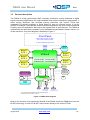
FM680 User Manual V1.6 FM680 User Manual for Virtex-6 XMC card 4DSP LLC, 955 S Virginia Street, Suite 214, Reno, NV 89502, USA 4DSP BV,Ondernemingsweg 66f, 2404 HN, Alphen a/d Rijn, Netherlands Email: [email protected] This document is the property of 4DSP and may not be copied nor communicated to a third party without the written permission of 4DSP. © 4DSP 2010 FM680 User Manual V1.6 Revision History Date Revision December 15, 2009 Version First release 1.0 Minor modifications 1.1 April 23 2010 Corrected typos 1.2 August 16 2010 Corrected typos 1.3 August 17 Added image 10 for the JTAG connector location 1.4 Updated block diagram Added detailed description for the XMC connector usage Removed reference to emcore connector and the QTE connector Updated PCIexpress connection diagram Added location images for LEDs and switch Added table to describe interFPGA pinout 1.5 28 Updated chapter 9.3 to add more detail with regards to the frontpanel optical transceivers 1.6 January 20, 2010 July 11 2012 August 2012 August 2012 FM680 User Manual www.4dsp.com -2- FM680 User Manual V1.6 Table of Contents 2 3 4 5 6 7 8 9 1.1 Acronyms ................................................................................................................ 4 1.2 Related Documents ................................................................................................. 4 1.3 General description ................................................................................................. 5 Installation ................................................................................................................... 6 2.1 Requirements and handling instructions .................................................................. 6 2.2 Firmware and software ............................................................................................ 6 Design .......................................................................................................................... 6 3.1 FPGA devices ......................................................................................................... 6 3.1.1 Virtex-5 device family and package .................................................................. 6 3.1.2 Virtex-6 device family and package .................................................................. 6 3.2 Inter-FPGA interface ............................................................................................... 6 3.3 PCI-express architecture ......................................................................................... 9 3.4 XMC P15 connector ...............................................................................................10 3.5 XMC P16 connector ...............................................................................................12 3.6 Pn4 user I/O connector ..........................................................................................13 3.7 Serial FLASH .........................................................................................................14 3.8 BLAST sites ...........................................................................................................14 3.9 External IO interfaces .............................................................................................15 3.9.1 Front Panel daughter card ...............................................................................15 3.9.2 Power connection to the front panel I/O daughter card ....................................19 3.9.3 Front Panel optical transceivers ......................................................................19 3.9.4 Optical transceiver MGT Reference Clock.......................................................21 3.10 FPGA LED ..........................................................................................................21 3.11 FPGA configuration ............................................................................................23 3.11.1 Flash storage ..................................................................................................23 3.11.2 CPLD device ...................................................................................................23 3.11.3 JTAG...............................................................................................................25 3.12 Clock tree ...........................................................................................................26 Power requirements ...................................................................................................27 4.1 External power connector for stand alone mode.....................................................30 Environment................................................................................................................31 5.1 Temperature ..........................................................................................................31 5.2 Convection cooling .................................................................................................31 5.3 Conduction cooling .................................................................................................31 Safety...........................................................................................................................31 EMC .............................................................................................................................31 Technical support .......................................................................................................32 Warranty ......................................................................................................................32 August 2012 FM680 User Manual www.4dsp.com -3- FM680 User Manual V1.6 Acronyms and related documents 1.1 Acronyms ADC DAC DCI DDR DSP EPROM FBGA FPDP FPGA JTAG LED LVTTL LVDS LSB LVDS MGT MSB PCB PCI PCI-e PLL PMC QDR SDRAM SRAM Analog to Digital Converter Digital to Analog Converter Digitally Controlled Impedance Double Data Rate Digital Signal Processing Erasable Programmable Read-Only Memory Fineline Ball Grid Array Front Panel Data Port Field Programmable Gate Array Joint Test Action Group Light Emitting Diode Low Voltage Transistor Logic level Low Differential Data Signaling Least Significant Bit(s) Low Voltage Differential Signaling Multi-Gigabit Transceiver Most Significant Bit(s) Printed Circuit Board Peripheral Component Interconnect PCI Express Phase Locked Loop PCI Mezzanine Card Quadruple Data rate Synchronous Dynamic Random Access memory Synchronous Random Access memory Table 1: Glossary 1.2 Related Documents IEEE Std 1386.1-2001: IEEE Standard Physical and Environmental Layers for PCI Mezzanine Cards (PMC). ANSI/VITA 20-2001 : Conduction Cooled PMC. ANSI/VITA 42.0-2005: XMC Switched Mezzanine Card Auxiliary Standard. ANSI/VITA 42.3-2006: XMC PCI Express Protocol Layer Standard IEEE Std 1386-2001: IEEE Standard for a Common Mezzanine Card (CMC) Family. Xilinx Virtex-5 Documentation Xilinx Virtex-6 Documentation August 2012 FM680 User Manual www.4dsp.com -4- FM680 User Manual 1.3 V1.6 General description The FM680 is a high performance XMC, optionally conduction cooled, dedicated to digital signal processing applications with high bandwidth and complex algorithms requirements. It offers various interfaces, fast on-board memory resources, one Virtex-5 FPGA with embedded PCI-express endpoint or Serial Rapid IO and one Virtex-6 device. It can be utilized, for example, to accelerate frequency-domain algorithms with off-the-shelf Intellectual Property cores for applications that require the highest level of performances. The FM680 is mechanically and electrically compliant to the standard and specifications listed in section 1.2 of this document. A top level diagram is depicted in Figure 1. Front Panel 180-pin QTH connector on side 1 and on side 2 (facing inward) or 4 optical tranceivers @ 2.5 Gb/s 128 Mb Serial flash BLAST SITE 1 BLAST SITE 4 Virtex-6 BLAST SITE 2 BLAST SITE 3 XC6VLX240T / XC6VLX550T XC6VSX315T / XC6VSX475T PCI express end point PCI express End point Pn4 User I/O 2 1 clocks Optional battery for IP encryption key LED x4 4x 2.5gbps 64 single ended (LVTTL or lower) or 32 LVDS pairs Flash 512Mbit 8x up to 5gbps x4 8x 2.5gbps 2 Virtex-5 LED 1 58 single ended Local bus 8 single ended 1 to/from Pn4 Configuration circuit and JTAG Optionally conduction cooled BLAST SITE 5 Pn5 PCI Express (VITA 42.3) Pn6 Rocket IO (VITA 42.2, 42.3) Only available on XC6VLX550T and SX475T FPGA devices 4 lanes go either to the V6 or to the V5 Figure 1: FM680 block diagram Build on the success of its predecessor boards of the FM48x series the FM680 also uses the BLAST technology. A total of 5 BLAST sites connect directly to the Virtex-6 FPGA. August 2012 FM680 User Manual www.4dsp.com -5- FM680 User Manual V1.6 BLAST, Board Level Advanced Scalable Technology, is a small PCB module that allows customization of the FM680 in memory extensions, processing units and communication interfaces. For more information about the available BLASTs on the FM680 please consult the following page: BLAST modules http://www.4dsp.com/BLAST.htm 2 Installation 2.1 Requirements and handling instructions 2.2 The FM680 must be installed on a motherboard compliant to the VITA 42.3 standard. Do not flex the board Observe ESD precautions when handling the board to prevent electrostatic discharges. Do not install the FM680 while the motherboard is powered up. Firmware and software Drivers, API libraries and a program example working in combination with a pre-programmed firmware for both FPGAs are provided. The FM680 is delivered with an interface to the Xilinx PCI-e endpoint core in the Virtex-5 device as well as an example VHDL design in the Virtex6 device so users can start performing high bandwidth data transfers over the PCI bus right out of the box. For more information about software installation and FPGA firmware, please refer the 4FM Get Started Guide. 3 Design 3.1 FPGA devices The Virtex-5 and Virtex-6 FPGA devices interface to the various resources on the FM680 as shown on Figure 1. They also interconnect to each other via 58 general purpose pins including 4 clock pins (2 pairs, one in each direction, 100Ω terminated). A 16 bits single ended bus is also available between the two FPGA devices for communication with the Pn4 bus or general purpose communication. 3.1.1 Virtex-5 device family and package The Virtex-5 device is from the Virtex-5 LX family. It can be either an XC5VLX20T or XC5VLX30T in a Fineline Ball Grid array with 323 balls (FF323). 3.1.2 Virtex-6 device family and package The Virtex-6 device is dedicated to Digital Signal Processing, video processing or communication applications and can be chosen from the SXT or LXT family devices. Its package is based on Fineline Ball Grid array with 1759 balls. In terms of logic and dedicated DSP resources, the FPGA B can be chosen from the following types: LX240T, LX550T, SX315T and the SX475T (FF1759). 3.2 Inter-FPGA interface The Virtex-5 device is connected to the Virtex-6 device using a 54 pin bus plus 2 differential clock signals. Also there are 16 single ended pins available that can be used as general August 2012 FM680 User Manual www.4dsp.com -6- FM680 User Manual V1.6 purpose IO or as a connection to the Pn4 bus. Please be aware that 8 of those extra bits are available only on the SX475T and the LX550T FPGA types. Virtex-5 (FPGA A) Virtex-6 (FPGA B) 2 GPIO GPIO CC 54 CC GPIO GPIO GPIO 8 GPIO GPIO 8 2 GPIO Only on LX550T and SX475T Figure 2: Inter-FPGA Interface By default 4DSP delivers a reference design that uses the interfpga bus to allow high speed data transfer and command distribution between the PCIexpress interface in the FPGA A and the FPGA B. The standard reference design does not implement the PN4 connection since those connections will depend on the user specific application. The user is free to modify the reference design and add specific features in FPGA A and FPGA B. The connections between the FPGA A and FPGA B are described in the following table. Table 2: interFPGA connections net name FPGA A bank FPGA A IO voltage FPGA A ball FPGA B bank FPGA B IO voltage FPGA B ball INTER_FPGA0 1 BLAST0_VIO A7 34 BLAST0_VIO AU13 INTER_FPGA1 1 BLAST0_VIO A6 34 BLAST0_VIO AR13 INTER_FPGA2 1 BLAST0_VIO E9 34 BLAST0_VIO AP13 INTER_FPGA3 1 BLAST0_VIO D8 34 BLAST0_VIO AN13 INTER_FPGA4 1 BLAST0_VIO D10 34 BLAST0_VIO AM13 INTER_FPGA5 1 BLAST0_VIO D9 33 BLAST0_VIO AK14 INTER_FPGA6 1 BLAST0_VIO C8 33 BLAST0_VIO AL14 INTER_FPGA7 1 BLAST0_VIO C7 33 BLAST0_VIO AM14 INTER_FPGA8 1 BLAST0_VIO B9 34 BLAST0_VIO AN14 INTER_FPGA9 1 BLAST0_VIO F8 34 BLAST0_VIO AR14 INTER_FPGA10 1 BLAST0_VIO B6 34 BLAST0_VIO AT14 INTER_FPGA11 1 BLAST0_VIO C6 34 BLAST0_VIO AV14 INTER_FPGA12 1 BLAST0_VIO A8 34 BLAST0_VIO BA14 INTER_FPGA13 1 BLAST0_VIO F7 34 BLAST0_VIO BB14 INTER_FPGA14 1 BLAST0_VIO A9 34 BLAST0_VIO BA15 INTER_FPGA15 1 BLAST0_VIO D7 34 BLAST0_VIO AY15 INTER_FPGA16 1 BLAST0_VIO E7 34 BLAST0_VIO AW15 INTER_FPGA17 1 BLAST0_VIO B10 34 BLAST0_VIO AV15 INTER_FPGA18 1 BLAST0_VIO C10 34 BLAST0_VIO AR15 INTER_FPGA19 11 BLAST0_VIO D13 34 BLAST0_VIO AP15 August 2012 FM680 User Manual www.4dsp.com -7- FM680 User Manual V1.6 INTER_FPGA20 11 BLAST0_VIO D14 33 BLAST0_VIO AN15 INTER_FPGA21 11 BLAST0_VIO E15 33 BLAST0_VIO AL15 INTER_FPGA22 11 BLAST0_VIO D15 33 BLAST0_VIO AK15 INTER_FPGA23 11 BLAST0_VIO E14 33 BLAST0_VIO AJ15 INTER_FPGA24 11 BLAST0_VIO F14 33 BLAST0_VIO AJ16 INTER_FPGA25 11 BLAST0_VIO A11 33 BLAST0_VIO AM16 INTER_FPGA26 11 BLAST0_VIO A12 33 BLAST0_VIO AN16 INTER_FPGA27 11 BLAST0_VIO C12 33 BLAST0_VIO AT16 INTER_FPGA28 11 BLAST0_VIO D18 34 BLAST0_VIO AV16 INTER_FPGA29 11 BLAST0_VIO B13 34 BLAST0_VIO AW16 INTER_FPGA30 11 BLAST0_VIO A13 34 BLAST0_VIO BA16 INTER_FPGA31 11 BLAST0_VIO G14 34 BLAST0_VIO BB16 INTER_FPGA32 11 BLAST0_VIO G15 34 BLAST0_VIO BB17 INTER_FPGA33 11 BLAST0_VIO B14 34 BLAST0_VIO AY17 INTER_FPGA34 11 BLAST0_VIO A14 34 BLAST0_VIO AW17 INTER_FPGA35 11 BLAST0_VIO G13 33 BLAST0_VIO AU17 INTER_FPGA36 11 BLAST0_VIO F13 33 BLAST0_VIO AT17 INTER_FPGA37 11 BLAST0_VIO C15 33 BLAST0_VIO AR17 INTER_FPGA38 11 BLAST0_VIO B15 33 BLAST0_VIO AM17 INTER_FPGA39 11 BLAST0_VIO B16 33 BLAST0_VIO AL17 INTER_FPGA40 11 BLAST0_VIO A16 33 BLAST0_VIO AK17 INTER_FPGA41 11 BLAST0_VIO F16 33 BLAST0_VIO AJ17 INTER_FPGA42 11 BLAST0_VIO G16 33 BLAST0_VIO AJ18 INTER_FPGA43 11 BLAST0_VIO A18 33 BLAST0_VIO AK18 INTER_FPGA44 11 BLAST0_VIO A17 33 BLAST0_VIO AN18 INTER_FPGA45 11 BLAST0_VIO E17 33 BLAST0_VIO AP18 INTER_FPGA46 11 BLAST0_VIO E16 33 BLAST0_VIO AR18 INTER_FPGA47 11 BLAST0_VIO C17 33 BLAST0_VIO AU18 INTER_FPGA48 11 BLAST0_VIO F17 33 BLAST0_VIO AV18 INTER_FPGA49 11 BLAST0_VIO D12 33 BLAST0_VIO AW18 INTER_FPGA50 11 BLAST0_VIO E12 33 BLAST0_VIO AY18 INTER_FPGA51 11 BLAST0_VIO C18 33 BLAST0_VIO BB18 INTER_FPGA52 11 BLAST0_VIO B18 33 BLAST0_VIO BB19 INTER_FPGA53 11 BLAST0_VIO F18 33 BLAST0_VIO BA19 INTER_FPGA_IO0 13 PN4_V H13 34 BLAST0_VIO AM12 INTER_FPGA_IO1 13 PN4_V H15 34 BLAST0_VIO AR12 INTER_FPGA_IO2 13 PN4_V H16 34 BLAST0_VIO AT12 INTER_FPGA_IO3 13 PN4_V L14 34 BLAST0_VIO AU12 INTER_FPGA_IO4 13 PN4_V K15 34 BLAST0_VIO AW12 INTER_FPGA_IO5 13 PN4_V L13 34 BLAST0_VIO BB13 INTER_FPGA_IO6 13 PN4_V J14 34 BLAST0_VIO AW13 INTER_FPGA_IO7 13 PN4_V J15 34 BLAST0_VIO AV13 August 2012 FM680 User Manual www.4dsp.com -8- FM680 User Manual V1.6 INTER_FPGA_IO8 13 PN4_V H18 21 BLAST0_VIO AW27 INTER_FPGA_IO9 13 PN4_V J18 21 BLAST0_VIO AW26 INTER_FPGA_IO10 13 PN4_V J17 21 BLAST0_VIO AW25 INTER_FPGA_IO11 13 PN4_V K17 21 BLAST0_VIO AY27 INTER_FPGA_IO12 13 PN4_V L17 21 BLAST0_VIO BA25 INTER_FPGA_IO13 13 PN4_V L16 21 BLAST0_VIO BA26 INTER_FPGA_IO14 13 PN4_V G18 21 BLAST0_VIO BB26 INTER_FPGA_IO15 13 PN4_V H17 21 BLAST0_VIO BB27 INTER_FPGA_CLK_A_to_Bn 4 2V5 V7 34 BLAST0_VIO AY13 INTER_FPGA_CLK_A_to_Bp 4 2V5 V8 34 BLAST0_VIO AY14 INTER_FPGA_CLK_B_to_An 4 2V5 P9 34 BLAST0_VIO AP12 INTER_FPGA_CLK_B_to_Ap 4 2V5 R9 34 BLAST0_VIO AP11 3.3 PCI-express architecture The Virtex-5 device is connected to the XMC connector (P15) and offers a PCI Express® Endpoint block integrated in the FPGA. The endpoint will support a 4 lanes generation 1 PCIexpress bus. A PCI express switch is used to optionally route the 4 lanes from the P15 connector to the Virtex-6 device instead of the Virtex-5 device. The remaining 4 transceiver lanes on the P15 connector are routed to the Virtex-6 device as well. This makes it possible to have an 8 lanes generation 1 PCI-express bus connecting to the Virtex-6 device. If this option is selected the 4 lanes connection towards the Virtex-5 device is not available. The standard reference design has the PCI Express connection towards the Virtex-5 FPGA. 4DSP can provide a reference design for the 8-lanes connection to the Virtex-6 FPGA. Please consult with your sales contact for more details. The following performances have been recorded with the FM680 transferring data on the bus using the standard 4DSP PCIe interface design: PCIe 1 lane: 150Mbytes/s sustained PCIe 4 lanes: 600Mbytes/s sustained PCIe 8 lanes: 800Mbytes/s sustained Higher performance transfers are possible but will require modifications to the PCIe interface design. Please consult with your sales contact for more details. Furthermore the VITA 42.3 standard defines an optional P16 connector which can carry an additional 8 lanes of high speed signaling. All these lanes are routed to the Virtex-6 device directly. An overview of the PCI-express subsystem is shown in Figure 3. August 2012 FM680 User Manual www.4dsp.com -9- FM680 User Manual V1.6 PCIe Switch PER0x 0 PET0x 0 PER0x 1 PET0x 1 PER0x 2 PET0x 2 XMC Pn5 PER0x 3 PET0x 3 PER0x 0 PET0x 0 PER0x 1 PET0x 1 PER0x 2 PET0x 2 Virtex 5 (FPGA A) MGT_112_0 MGT_112_1 MGT_114_0 MGT_114_1 MGTREFCLK_112 select Pci_select PER0x 0 PET0x 0 PER0x 1 PET0x 1 PER0x 2 PET0x 2 PER0x 3 PET0x 3 RefCLK CLK buffer PER0x 4 PET0x 4 PER0x 5 PET0x 5 PER0x 6 PET0x 6 PER0x 7 PET0x 7 Virtex 6 (FPGA B) MGT_112_0 MGT_112_1 MGT_112_2 PER0x 3 PET0x 3 MGT_112_3 PER0x 4 PET0x 4 MGT_113_0 PER0x 5 PET0x 5 MGT_113_1 PER0x 6 PET0x 6 MGT_113_2 PER0x 7 PET0x 7 MGT_113_3 MGTREFCLK_112_0 XMC Pn6 PER1x 0 PET1x 0 PER1x 1 PET1x 1 PER1x 2 PET1x 2 PER1x 0 PET1x 0 PER1x 1 PET1x 1 PER1x 2 PET1x 2 PER0x 3 PET0x 3 PER0x 3 PET0x 3 RefCLK CLK buffer MGT_114_0 MGT_114_1 MGT_114_2 MGT_114_3 RefCLK MGTREFCLK_114_0 RefCLK MGTREFCLK_115_1 PER1x 4 PET1x 4 PER0x 4 PET1x 4 PER1x 5 PET1x 5 PER1x 5 PET1x 5 MGT_115_1 PER1x 6 PET1x 6 PER1x 6 PET1x 6 MGT_115_2 PER1x 7 PET1x 7 PER1x 7 PET1x 7 MGT_115_3 MGT_115_0 Figure 3: PCI-express subsystem diagram. NOTE: There is a swap between the PET0TX0 and PET0TX1 on the FM680. 3.4 XMC P15 connector The Table 3 shows the pin out as defined by VITA 42.3. Only the highlighted pins are connected on the FM680. Table 4 indicates the signals usage and on board connections. August 2012 FM680 User Manual www.4dsp.com - 10 - FM680 User Manual V1.6 Table 3: XMC P15 pin out as per VITA 42.3 A B C D E F 1 PET0p0 PET0n0 3.3V PET0p1 PET0n1 VPWR 2 GND GND TRST# GND GND MRSTI# 3 PET0p2 PET0n2 3.3V PET0p3 PET0n3 VPWR 4 GND GND TCK GND GND MRSTO# 5 PET0p4 PET0n4 3.3V PET0p5 PET0n5 VPWR 6 GND GND TMS GND GND +12V 7 PET0p6 PET0n6 3.3V PET0p7 PET0n7 VPWR 8 GND GND TDI GND GND -12V 9 RFU RFU RFU RFU RFU VPWR 10 GND GND TDO GND GND GA0 11 PER0p0 PER0n0 MBIST# PER0p1 PER0n1 VPWR 12 GND GND GA1 GND GND MPRESENT# 13 PER0p2 PER0n2 3.3VAUX PER0p3 PER0n3 VPWR 14 GND GND GA2 GND GND MSDA 15 PER0p4 PER0n4 RFU PER0p5 PER0n5 VPWR 16 GND GND MVMRO GND GND MSCL 17 PER0p6 PER0n6 RFU PER0p7 PER0n7 RFU 18 GND GND RFU GND GND RFU 19 REFCLK+0 REFCLK-0 RFU WAKE# ROOT0# RFU Table 4: XMC P15 connections FPGA Pin V5_U8 Name/Description PCIexpress reset input XMC P15 FPGA Bank DIR 4 I F2 MRSTI# Pin Number Pin Name n.a. Connected to GND n.a. O F12 MPRESENT# n.a. Not connected n.a. O C11 MBIST# n.a. Conencted to TDO n.a. I C8 TDI n.a. Conencted to TDI n.a. O C10 TDO n.a. VPOWER is used to generate local 5V n.a. I … n.a. General ground for FM680 n.a. I … n.a. Connects to -12V of daughter card. n.a. I F8 n.a. Connects to +12V of daughter card. and is used for on board voltage control circuits n.a. I F6 n.a. Used directly n.a. I … Refer to Figure 3 Connects to Virtex-5 and Virtex-6 n.a. O Refer to Figure 3 Connects to Virtex-5 and Virtex-6 n.a. August 2012 VPWR GND -12V +12V I … … FM680 User Manual www.4dsp.com 3.3V PET0p/n[7..0] PER0p/n[7..0] - 11 - FM680 User Manual 3.5 V1.6 XMC P16 connector The Table 5 shows the pin out as defined by VITA 42.3. Only the highlighted pins are connected on the FM680. Table 6 indicates the signals usage and on board connections. Table 5: XMC P15 pin out as per VITA 42.3 A B C D E F 1 PET1p0 PET1n0 UD PET1p1 PET1n1 UD 2 GND GND UD GND GND UD 3 PET1p2 PET1n2 UD PET1p3 PET1n3 UD 4 GND GND UD GND GND UD 5 PET1p4 PET1n4 UD PET1p5 PET1n5 UD 6 GND GND UD GND GND UD 7 PET1p6 PET1n6 UD PET1p7 PET1n7 UD 8 GND GND UD GND GND UD 9 RFU RFU UD RFU RFU UD 10 GND GND UD GND GND UD 11 PER1p0 PER1n0 UD PER1p1 PER1n1 UD 12 GND GND UD GND GND UD 13 PER1p2 PER1n2 UD PER1p3 PER1n3 UD 14 GND GND UD GND GND UD 15 PER1p4 PER1n4 UD PER1p5 PER1n5 UD 16 GND GND UD GND GND UD 17 PER1p6 PER1n6 UD PER1p7 PER1n7 UD 18 GND GND UD GND GND UD 19 REFCLK+1 REFCLK-1 UD RFU ROOT1# UD Table 6: XMC P16 connections FPGA Pin Name/Description Refer to Figure 3 Connects to Virtex-6 Refer to Figure 3 Connects to Virtex-6 August 2012 XMC P15 FPGA Bank DIR n.a. O n.a. I Pin Number Pin Name … PET1p/n[7..0] … FM680 User Manual www.4dsp.com PER1p/n[7..0] - 12 - FM680 User Manual 3.6 V1.6 Pn4 user I/O connector The Pn4 connector is connected to the Virtex-5 device. Connector pin Signal name FPGA pin 1 Pn4_IO0 R1 3 Pn4_IO2 5 Signal name Connector pin T1 Pn4_IO1 2 V1 U1 Pn4_IO3 4 Pn4_IO4 P2 P3 Pn4_IO5 6 7 Pn4_IO6 V2 V3 Pn4_IO7 8 9 Pn4_IO8 R2 T2 Pn4_IO9 10 11 Pn4_IO10 U4 U3 Pn4_IO11 12 13 Pn4_IO12 K12 L18 Pn4_IO13 14 15 Pn4_IO14 M11 K16 Pn4_IO15 16 17 Pn4_IO16 M14 M13 Pn4_IO17 18 19 Pn4_IO18 M16 M15 Pn4_IO19 20 21 Pn4_IO20 M10 N11 Pn4_IO21 22 23 Pn4_IO22 T17 T16 Pn4_IO23 24 25 Pn4_IO24 T12 R12 Pn4_IO25 26 27 Pn4_IO26 T18 U18 Pn4_IO27 28 29 Pn4_IO28 P10 N10 Pn4_IO29 30 31 Pn4_IO30 U16 U15 Pn4_IO31 32 33 Pn4_IO32 V18 V17 Pn4_IO33 34 35 Pn4_IO34 R10 R11 Pn4_IO35 36 37 Pn4_IO36 V16 V15 Pn4_IO37 38 39 Pn4_IO38 T11 U11 Pn4_IO39 40 41 Pn4_IO40 R14 T14 Pn4_IO41 42 43 Pn4_IO42 V10 U10 Pn4_IO43 44 45 Pn4_IO44 U14 T13 Pn4_IO45 46 47 Pn4_IO46 P12 P13 Pn4_IO47 48 49 Pn4_IO48 U13 V13 Pn4_IO49 50 51 Pn4_IO50 V12 V11 Pn4_IO51 52 53 Pn4_IO52 R17 R16 Pn4_IO53 54 55 Pn4_IO54 R15 P18 Pn4_IO55 56 57 Pn4_IO56 K14 P15 Pn4_IO57 58 59 Pn4_IO58 N18 N17 Pn4_IO59 60 61 Pn4_IO60 N16 N15 Pn4_IO61 62 Pn4_IO62 N13 N12 Pn4_IO63 64 63 FPGA pin Table 7 : Pn4 pin assignment August 2012 FM680 User Manual www.4dsp.com - 13 - FM680 User Manual 3.7 V1.6 Serial FLASH A 128 Mbits serial flash device (S25FL128P) is available to the Virtex-6 device. This flash allows the storage of vital data like processor boot code and settings into a non volatile memory. The flash is operated using a standard SPI interface that can run up to 104 MHz, allowing for a page programming speed up to 208 KB/s. Reading data from the flash can be done at speeds up to 13 MB/s. The SPI programming pins is connected to a bank that supports 1V8, whereas the serial flash is operating at 3V3. This will not cause problems for the signals from the Virtex-6 to the flash device but the signal from the flash device to the Virtex-6 are passed through a level translator (SN74AVC4T245). 3.8 BLAST sites Thanks to the availability of 5 BLAST sites a wide variety of memory and processing modules can be connected to the Virtex-6 device. For each BLAST site it is possible to choose from the list of available BLAST modules. For more information about the available BLASTs on the FM680 please consult the following page: BLAST modules http://www.4dsp.com/BLAST.htm Table 8: BLAST Configuration Options BLAST SITE 1 2 3 4 5(3) Single BLAST YES YES YES YES YES Single Extended BLAST(1) YES YES YES YES YES Double BLAST(2) YES YES YES YES Double Extended BLAST(1)(2) YES YES YES YES 1) Single and double extended BLAST placed in BLAST sites 4 and 5 will protrude 3mm from edge of the board. 2) BLAST SITES 1 and 2, 4 and 5 are paired when using double BLAST. 3) Only available on XC6VLX550T and SX475T FPGA devices August 2012 FM680 User Manual www.4dsp.com - 14 - FM680 User Manual V1.6 Table 9: BLAST Memory/Processing Options BLAST SITE 1 2 3 4 5(1) DDR3 YES YES YES YES NO DDR2 YES YES YES YES NO QDR YES YES YES YES YES ADV212 JPEG2000 YES YES YES YES YES 32GB NAND FLASH YES YES YES YES YES 1) Only available on XC6VLX550T and SX475T FPGA devices Due to its small form factor and ease of design, the BLAST modules enable a rapid solution for custom memory or processing requirements. 3.9 External IO interfaces The Virtex-6 device interfaces to the front panel daughter card on the FM680 via a high speed connector. 174 I/Os are available from the FPGA to/from the daughter card that can be mounted in the IO area defined by the XMC standard. As an alternative solution it is also possible to have 4 optical transceivers in the IO area. 3.9.1 Front Panel daughter card (Only available with front panel daughter card purchase and not in combination with the optical transceivers) The Virtex-6 device interfaces to a 180-pin connector placed in the Front panel I/O area (on both side 1 of the PCB). It serves as a base for a daughter card and offers I/O diversity to the FM680 PMC. The FPGA I/O banks are powered either by 1.8V or 2.5V via a large 0 ohms resistor (2.5V is the default if not specified otherwise at the time of order). Using the Xilinx DCI termination options to match the signals impedance allows many electrical standards to be supported by this interface. The VRN and VRP pins on the I/O banks connected to the daughter card connector are respectively pulled up and pulled down with 50Ω resistors in order to ensure optimal performances when using the Xilinx DCI options. The VREF pins are connected to 0.9V for DDR2 DCI terminations. Please, contact 4DSP Inc. for more information about available daughter card types. The 180-pin Samtec connector pin assignment is as follows. All signals shown as LVDS pairs in the table can also be used for any standard that does not breach the electrical rules of the Xilinx I/O pad. The FP_Xi signals in the table below are routed as single ended. August 2012 FM680 User Manual www.4dsp.com - 15 - FM680 User Manual V1.6 Connector pin Signal Name FPGA pin FPGA pin Signal name Connector pin 1 FP_P0 J12 A16 FP_P1 2 FP_N0 J11 B16 FP_N1 4 FP_X0 C13 D12 FP_X1 6 (2) M13 J13 FP_P3 8 (2) FP_N2 N13 K13 FP_N3 10 FP_X2 K14 L14 FP_X3 12 FP_P4 H13 D16 FP_P5 14 FP_N4 G12 C16 FP_N5 16 17 FP_X4 H15 G14 FP_X5 18 19 FP_P6 F12 D13 FP_P7 20 21 FP_N6 E12 E13 FP_N7 22 23 FP_X6 E15 F15 FP_X7 24 25 FP_P8 B14 A15 FP_P9 26 27 FP_N8 C14 A14 FP_N9 28 29 FP_X8 C15 D15 FP_X9 30 (2) M14 M16 FP_P11 32 (2) FP_N10 N14 N15 FP_N11 34 FP_X10 H14 G13 FP_X11 36 FP_P12 A17 L16 FP_P13 38 FP_N12 B17 L15 FP_N13 40 FP_X12 J16 H16 FP_X13 42 FP_P14 D18 K17 FP_P15 44 FP_N14 C18 J17 FP_N15 46 FP_X14 M18 N18 FP_X15 48 (2) N16 L12 (2) FP_N16 P16 M12 FP_N17 FP_X16 K18 J18 FP_X17 54 (1) E14 H18 FP_P19 56 (1) G18 FP_N19 58 F16 FP_X19 60 3 5 7 FP_P2 9 11 13 15 31 33 35 37 39 41 43 45 47 49 51 53 55 FP_P10 FP_P16 FP_P18 57 FP_N18 F14 59 FP_X18 G16 FP_P17 (1) 50 (1) 52 Table 10 : Front Panel IO daughter card pin assignment Bank A (1) (2) August 2012 Connected to a global clock pin on the FPGA. LVDS output not supported. Connected to a regional clock pin on the FPGA. LVDS output not supported. FM680 User Manual www.4dsp.com - 16 - FM680 User Manual V1.6 Connector pin Signal Name FPGA pin FPGA pin Signal name Connector pin 61 FP_P20 G19 E19 FP_P21 62 FP_N20 F19 E18 FP_N21 64 FP_X20 C19 B19 FP_X21 66 FP_P22 F17 B18 FP_P23 68 FP_N22 G17 A19 FP_N23 70 FP_X22 J15 K15 FP_X23 72 (2) P18 G23 FP_P25 74 (2) FP_N24 P17 H23 FP_N25 76 77 FP_X24 D17 E17 FP_X25 78 79 FP_P26 B24 C24 FP_P27 80 81 FP_N26 A24 C23 FP_N27 82 83 FP_X26 G22 F22 FP_X27 84 85 FP_P28 B23 H21 FP_P29 86 87 FP_N28 B22 J21 FP_N29 88 89 FP_X28 F21 E22 FP_X29 90 FP_P30 E24 C21 FP_P31 92 FP_N30 E23 D21 FP_N31 94 FP_X30 H20 G21 FP_X31 96 FP_P32 K20 A22 FP_P33 98 FP_N32 L20 A21 FP_N33 100 FP_X32 D23 D22 FP_X33 102 FP_P34 B21 J22 FP_N34 A20 K22 FP_N35 FP_X34 J20 H19 FP_X35 L22 L21 63 65 67 69 71 73 FP_P24 75 91 93 95 97 99 101 103 105 107 109 111 (2) FP_P36 3.3V/2.5V/1.8V 113 FP_X36 115 FP_P35 L19 104 (2) 106 FP_N36 Vbatt K19 (2) 108 (2) (3) 110 112 FP_X37 114 3.3V/2.5V/1.8V 0.9V 116 117 3.3V/2.5V/1.8V 3.3V/2.5V/1.8V 118 119 FP_X38 FP_X39 120 F32 F31 Table 11: Front Panel IO daughter card pin assignment Bank B (1) (2) (3) August 2012 Connected to a global clock pin on the FPGA. LVDS output not supported. Connected to a regional clock pin on the FPGA. LVDS output not supported. Vbatt is connected to both Virtex devices Vbatt pin. FM680 User Manual www.4dsp.com - 17 - FM680 User Manual V1.6 Connector pin Signal Name FPGA pin FPGA pin Signal name Connector pin 121 FP_P37 E32 C20 FP_P38 122 FP_N37 D32 D20 FP_N38 124 FP_X40 E35 D35 FP_X41 126 FP_P39 B33 A32 FP_P40 128 FP_N39 C33 B32 FP_N40 130 FP_X42 G33 G32 FP_X43 132 FP_P41 H31 A34 FP_P42 134 FP_N41 G31 A35 FP_N42 136 137 FP_X44 D33 E33 FP_X45 138 139 FP_P43 L29 B34 FP_P44 140 141 FP_N43 L30 C34 FP_N44 142 143 FP_X46 123 125 127 129 131 133 135 145 J32 J31 FP_X47 144 (1) A36 M28 FP_P46 146 (1) FP_P45 147 FP_N45 B36 M29 FP_N46 148 149 FP_X48 K29 K30 FP_X49 150 FP_P47 H30 C35 FP_P48 152 FP_N47 J30 C36 FP_N48 154 FP_X50 AH31 AG31 FP_X51 156 FP_P49 D36 E34 FP_P50 158 FP_N49 D37 F34 FP_N50 160 FP_X52 AH29 AG29 FP_X53 162 FP_P51 T30 AG32 FP_P52 164 FP_N51 R30 AF31 FP_N52 166 FP_X54 AH30 AJ30 FP_X55 168 (2) N33 R32 FP_P54 170 (2) FP_N53 P33 T32 FP_N54 172 FP_X56 V31 W31 FP_X57 174 (1) AD31 AK33 FP_P56 176 (1) AJ32 FP_N56 178 AK30 FP_X59 180 151 153 155 157 159 161 163 165 167 169 171 173 175 FP_P53 FP_P55 177 FP_N55 AD30 179 FP_X58 AJ31 Table 12 : Front Panel IO daughter card pin assignment Bank C August 2012 FM680 User Manual www.4dsp.com - 18 - FM680 User Manual V1.6 3.9.2 Power connection to the front panel I/O daughter card The Front Panel I/O daughter card on side 1 of the PCB is powered via a 7-pin connector of type BKS (Samtec). Each pin can carry up to 1.5A. The power connector’s pin assignment is as follows. Pin # 1 3 5 Signal +3.3V +5V +12V 7 -12V Signal +3.3V GND GND Pin # 2 4 6 Table 13: Daughter card power connector pin assignment on PMC side 1 3.9.3 Front Panel optical transceivers (Special build option and not in combination with the front panel daughter card) Four 2.5 GB/s optical transceivers (LTP-ST11M) are available on the FM680 in the front panel area. They are connected to the MGT I/Os of the Virtex-6. Infiniband protocols as well as Gigabit Ethernet and Fibre channel (sFPDP) can be implemented over the transceivers. Lower rate optical transceivers (2.125 GB/s and 1.0625 GB/s) are available in the same form factor. The Figure 4 shows the block diagram of the optical transceivers on the FM680 and Figure 5 shows the location of the optical transceivers on the PCB. Table 14 shows the pin assignments for each serial lane and the optical transceiver it connects to. 125 MHz Clk buffer (874003BG-05LF) QA0 Virtex 6 B) AB31(FPGA OT3 OT2 OT1 OT0 TX RX TX RX TX RX TX en MGT_116_3 en MGT_116_2 en MGT_116_1 en MGT_116_0 RX AA30 MGTREFCLK_116_0 Figure 4: Optical transceiver connections August 2012 FM680 User Manual www.4dsp.com - 19 - FM680 User Manual V1.6 OT0 OT1 OT2 OT3 Figure 5: Optical transceiver locations Table 14: Optical transceiver MGT connections FPGA Pin August 2012 Net Name K4 MGT_FP_RXp3 K3 MGT_FP_TXp3 J6 MGT_FP_RXn3 J5 MGT_FP_RXp3 L2 MGT_FP_RXp2 L1 MGT_FP_TXp2 L6 MGT_FP_RXn2 L5 MGT_FP_RXp2 M4 MGT_FP_RXp1 M3 MGT_FP_TXp1 N6 MGT_FP_RXn1 N5 MGT_FP_RXp1 N2 MGT_FP_RXp0 N1 MGT_FP_TXp0 P8 MGT_FP_RXn0 P7 MGT_FP_RXp0 MGT Block Optical transceiver 116_3 OT3 116_2 OT2 116_1 OT1 116_0 OT0 FM680 User Manual www.4dsp.com - 20 - FM680 User Manual V1.6 3.9.4 Optical transceiver MGT Reference Clock A low jitter oscillator connects to the 874003BG-05LF. Depending on the resistor configuration this device can output a 312.5, 156.25 or 125 MHz clock. The default configuration outputs a 156.25 MHz reference clock. The Figure 6 and Table 15 show the selection resistor locations and type. Table 15: Optical transceiver reference clock frequency selection resistors Resistor Type MGT REFCLK R510 Pull up (default) R518 Pull down R294 Pull up (default) R494 Pull down R292 Pull up (default) R293 Pull down FSEL0 FSEL1 FSEL2 518 510 R294 R494 R292 R293 Figure 6: Optical transceiver reference clock selection resistors locations 3.10 FPGA LED Four LEDs are connected to the Virtex-5 device. In the default FPGA firmware, the LEDs are driven by the Virtex-5 device. The following table shows the meaning of the LEDs in the standard reference design. OFF ON FLASHING LED 0 (red) PCIexpresslink down PCIexpress link up n.a. LED 1 (red) No PCI express traffic PCI express traffic PCI express traffic LED 2 (red) No PCI express traffic PCI express traffic PCI express traffic LED 3 (red) FM680 PCB revision 2 FM680 PCB revision 1 (only when FPGA A firmware revision is 2.3 or higher) n.a. Table 16: LED board status August 2012 FM680 User Manual www.4dsp.com - 21 - FM680 User Manual V1.6 The LEDs are located on side 2 of the PCB in the front panel area. Their locations are depicted in Figure 7. CPLD_LED0 CPLD_LED1 CPLD_LED2 CPLD_LED3 FPGA_LED1 FPGA_LED0 FPGA_LED3 FPGA_LED2 Figure 7: FPGA and CPLD LED locations To turn on a LED drive the signal low. To turn a LED off, make the signal high. FPGA Pin Net Name FPGA Bank DIR C13 FPGA_LED0 11 O C16 FPGA_LED1 11 O D17 FPGA_LED2 11 O B11 FPGA_LED3 11 O Table 17: FPGA LED connections The I/O standard to be assigned depends on BLAST configuration. August 2012 FM680 User Manual www.4dsp.com - 22 - FM680 User Manual V1.6 3.11 FPGA configuration 3.11.1 Flash storage The FPGA firmware is stored on board in a flash device. The 512Mbit device is partly used to store the configuration for both FPGAs. In the default CPLD firmware configuration, the Virtex-5 device and the Virtex-6 device are directly configured from flash if a valid bit stream is stored in the flash for each FPGA. The flash is preprogrammed in factory with the default firmware example for both FPGAs. JTAG Header S29GL512M 512Mbit Flash Virtex-6 JTAG 8-bit parallel configuration JTAG JTAG CoolRunner-II CPLD XC2C256 CP132 DIP switch Virtex-5 LED x4 Figure 8 : Configuration circuit 3.11.2 CPLD device As shown on Figure 7, a Cool Runner-II CPLD is present on board to interface between the flash device and the FPGA devices. The CPLD is used to program and read the flash. The data stored in the flash is transferred from the host motherboard via the PCI-express bus to the Virtex-5 device and then to the CPLD that writes the required bit stream to the storage device. A 31.25 MHz clock connects to the CPLD and is used to generate the configuration clock sent to the FPGA devices. At power up, if the CPLD detects that an FPGA configuration bit stream is stored in the flash for both FPGA devices, it will start programming the devices in SelecMap mode. Do NOT reprogram the CPLD without 4DSP’s approval The CPLD configuration is achieved by loading with a Xilinx download cable a bit stream from a host computer via the JTAG connector. The FPGA devices configuration can also be achieved via the JTAG chain. August 2012 FM680 User Manual www.4dsp.com - 23 - FM680 User Manual V1.6 3.11.2.1 DIP Switch A switch (J1) is located next to the JTAG programming connector (J6) see Figure 9. The switch positions are defined as follows: J1 SW4 SW3 SW2 SW1 Figure 9: switch (J1) location Sw1 OFF Default setting. The Virtex-5 device configuration is loaded from the flash at power up. ON Virtex-5 device safety configuration loaded from the flash at power up. To be used only if the Virtex-5 device cannot be configured or does not perform properly with the switch in the OFF position. Sw2 Reserved (should be OFF) Sw3 Reserved (should be ON) Sw4 Reserved (should be OFF) Table 18: Switch description 3.11.2.2 LED and board status Four LEDs connect to the CPLD and give information about the board status. August 2012 FM680 User Manual www.4dsp.com - 24 - FM680 User Manual V1.6 OFF ON FLASHING LED 0 (red) FPGA A configured FPGA A not configured FPGA A or B bit stream or user_ROM_register is currently being written to the flash LED 1 (red) FPGA B configured FPGA B not configured FPGA A or B bit stream or user_ROM_register is currently being written to the flash LED 2 (red) FLASH idle FLASH busy Safety configuration loaded into FPGA A, or attempted to load. LED 3 (red) No CRC error detected CRC error. Presumably a wrong or corrupted FPGA bit stream has been written to the flash. Once on this LED remains on n.a. Table 19: LED board status The LEDs are located on side 2 of the PCB in the front panel area. Their locations are depicted in Figure 7. 3.11.3 JTAG A JTAG connector is available on the FM680 for configuration purposes. The JTAG can also be used to debug the FPGA design with the Xilinx Chipscope. A press fit connector is delivered with the board that can be plugged into the connector holes. The JTAG connector can be placed on both sides of the PCB. The connector location seen from the bottom of the PCB is shown in Figure 10. August 2012 FM680 User Manual www.4dsp.com - 25 - FM680 User Manual V1.6 VCC GND TCK 1 4 2 5 3 6 TMS TDI TDO Figure 10: JTAG connector (J6) location The JTAG connector pinout is as follows: Pin # 1 2 3 Signal 1.8V GND TCK Signal TMS TDI TDO Pin # 4 5 6 Table 20 : JTAG pin assignment 3.12 Clock tree The FM680 clock architecture offers an efficient distribution of low jitter clocks. Both FPGA devices receive a low jitter 125MHz clock. A low jitter programmable clock able to generate frequencies from 62.5MHz to 255.5MHz in steps of 0.5MHz is also available. This clock management approach ensures maximum flexibility to efficiently implement multiclock domains algorithms and use the memory devices at different frequencies. Both clock buffer devices (CDCV1804) and the frequency synthesizer (CDCE925) are controlled by the Virtex-5 device. August 2012 FM680 User Manual www.4dsp.com - 26 - FM680 User Manual V1.6 Y2 125 MHz P8/P7 Y1 Virtex-5 (FPGA_A) Y0 Y3 T6 CDCM1804 CDCE925 AE30/AF30 W30/V30 16 MHz Y4 Y5 Y30 Virtex 6 (FPGA_B) AA31 Y1 CPLD Figure 11 : Clock tree CDCE925, CDCV1804 FPGA Pin Net Name DIR Device Pin Number Pin Name V5_T6 CLK_SYNTH_A I CDCE925 13 Y1 V6_Y30 CLK_SYNTH_B I CDCE925 7 Y4 V6_AA31 CLK_SYNTH_B I CDCE925 8 Y5 CDCV1804 10 Y2- CDCV1804 9 Y2+ CDCV1804 16 Y0- CDCV1804 15 Y0+ CDCV1804 22 Y1- CDCV1804 21 Y1+ V5_P7 CLK125_AN I V5_P8 CLK125_AP V6_V30 CLK125_B0N V6_W30 CLK125_B0P V6_AF30 CLK125_B1N V6_AE30 CLK125_B1P I I Table 21: Miscellaneous clock connections 4 Power requirements The Power is supplied to the FM680 via the XMC Pn5 connector. Several DC-DC converters generate the appropriate voltage rails for the different devices and interfaces present on board. The FM680 power consumption depends mainly on the FPGA devices work load. By using high efficiency power converters, all care has been taken to ensure that power consumption will remain as low as possible for any given algorithm. After power up, the FM680 typically consumes 6 Watts of power. For precise power measurements it is recommended to use the Xilinx power estimation tools for both the Virtex5 and Virtex-6 FPGA devices. The maximum current rating given in the table below is the maximum current that can be drawn from each voltage rail in the case resources are used to their maximum level. Special precautions need to be taken to support the XMC VPOWER input, since the XMC standard dictates that this power supply can either be 12V or 5V. To overcome this, a voltage detection circuit detects whether VPOWER is 12V or 5V and enables a switching regulator or August 2012 FM680 User Manual www.4dsp.com - 27 - FM680 User Manual V1.6 a Field Effect Transistor (FET). If VPOWER is 12V the switching regulator converts down to 5V otherwise the FET allows 5V to pass through. Device/Interface Voltage Maximum current rating DCI and memory reference voltage 0.9V 6A Virtex-6 device core 1.0V 10 A Virtex-5 device core 1.0V 2A BLAST core and IO,Virtex-6 I/O banks 1.8V 6A Virtex-5 device I/O bank connected to the front panel daughter card 0.9/1.0/1.8/2.5/3. 3V …A front Panel I/O daughter card 5V 1A Front Panel IO daughter card 3V3 3A Front Panel IO daughter card 12V 1A Front Panel IO daughter card -12V 1A MGT power supply 1.0V, 1.2V, 2.5V 2.0A, 2.5A, 0.01A respectively Table 22 : Power supply Optionally, the FM680 can be used as a standalone module and is powered via the external power connector. August 2012 FM680 User Manual www.4dsp.com - 28 - FM680 User Manual 12v to 5v0 LTC3605 Iout - 6A V1.6 5v to 1v0 EN5396QI - V6 @ 5A - V5 @ 1A 1v0 FET 5V0 XMC VPWR 5V /12V @12A 5v to 1v0 EN5396QI - V6 @ 5A - V5 @ 1A BLAST voltage*5 1v5/1v8 5A BLAST@ voltage*4 BLAST@voltage*4 1v5/1v8 6voltage*4 A BLAST 1v5/1v8 3v3 @ 2A @ 6 A 1v5/1v8 3v3 @ 2A @ 6 A 3v3 @ 2A ENABLE CONTROL 5v to 1v8 EN5395QI - MGT @ 2.5A - BLAST @ 5A 1v8 1v8 to 1v2 TPS74401 5V to 0v9 TPS54972 - ddr term @7A 1v8 to 1v5 TPS74401 1v2 0v9 5V 3v3 to 2v5 TPS74401 MGT @ <1 VADJ @ 3A 2V5 3v3 XMC 3v3 @8A 3v3 to 1v2 EN5395QI - MGT @ 2 A 1V2 1v2 to 1v0 TPS74401 1v0 XMC -12v Figure 12 : Power supply An ADT7411 device is used to monitor the power on the different voltage rails as well as the temperature. The ADT7411 data are constantly passed to the Virtex-6 device. Measurements can be accessed from the host computer via the PCI bus. A software utility delivered with the board allows the monitoring of the voltage on the 2.5V, 1.8V, 1.2V, 1.0V and 0.9V rails. It also displays both FPGAs junction temperature. August 2012 FM680 User Manual www.4dsp.com - 29 - FM680 User Manual 4.1 V1.6 External power connector for stand alone mode An external power connector (J2) is available on side 2 of the PMC, next to the PMC connectors. It is used to power the board when it is in stand alone mode. This is a right angled connector and it is mounted on board only if the card is ordered as a stand alone version (FM680-SA). The height and placement of this connector on the PCB breaches the PMC specifications and the module should not be used in an enclosed chassis compliant to PMC specifications if the external power connector is present on board. Do not connect an external power source to J2 if the board is powered via the XMC connectors. Doing so will result in damaging the board. The external power connector is of type Molex 43045-1021. Each circuit can carry a maximum current of 5A. The connector pin assignment is as follows: Pin # 1 3 5 7 9 Signal 3.3V 5V GND GND -12V Signal 3.3V 5V GND GND 12V Pin # 2 4 6 8 10 Table 23 : External power connector pin assignment WARNING: UNREGULATED UNPROTECTED EXTERNAL POWER SUPPLY CONNECTION This board is designed with an UNSUPPORTED feature for an external power connector labeled as J2. Mounting a connector on the PCB breaches the PMC electrical and mechanical specifications of the PMC standard. This is a FACTORY ONLY feature that is used in the manufacturing process when powering the board is required in an UNMOUNTED PCI bus mode, thus in stand alone mode. DO NOT connect an external power source to J2, doing so may result in damaging the board and will automatically VOID WARRANTY. Consult factory for further information. August 2012 FM680 User Manual www.4dsp.com - 30 - FM680 User Manual V1.6 5 Environment 5.1 Temperature Operating temperature 0°C to +60°C (Commercial) -40°C to +85°C (Industrial) Storage temperature: -40°C to +120°C 5.2 Convection cooling 600LFM minimum 5.3 Conduction cooling The FM680 can optionally be delivered as conduction cooled PMC. The FM680 is compliant to ANSI/VITA 20-2001 standard for conduction cooled PMC. 6 Safety This module presents no hazard to the user. 7 EMC This module is designed to operate from within an enclosed host system, which is build to provide EMC shielding. Operation within the EU EMC guidelines is not guaranteed unless it is installed within an adequate host system. This module is protected from damage by fast voltage transients originating from outside the host system which may be introduced through the system. August 2012 FM680 User Manual www.4dsp.com - 31 - FM680 User Manual V1.6 8 Technical support Technical support for all 4DSP Product, hardware, software and firmware is available under 4DSP Terms and Conditions of Sales ONLY in its original condition AS-SHIPPED unless agreed to by 4DSP and documented in writing, prior to any modifications. Terms and Conditions are available from http://www.4dsp.com/TCs.txt Technical support requests should be sent to [email protected] Any electrical connections made to the board or other components shall be made only with approved connectors as specifically identified in the products official documentation. Any modification to hardware including but not limited to removing of components, soldering or other material changes to in part or in whole to the PCM and/or its components will immediately invalidate and make void any warranty or extended support if any. Further, and changes or modifications to software and/or firmware supplied with the Product, unless provided for in the Products official documentation, shall immediately invalidate and make void any warranty or extended support if any. 9 Warranty Hardware Software/Firmware Basic Warranty (included) 1 Year from Date of Shipment 90 Days from Date of Shipment Extended Warranty (optional) 2 Years from Date of Shipment 1 Year from Date of Shipment August 2012 FM680 User Manual www.4dsp.com - 32 -