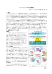
1
HELIX SINGLE BOARD COMPUTER
PC/104 SBC with Vortex Processor
and Dual 10/100 Ethernet Switch
Rev A: December 2011
Revision
Date
A
12/15/2011
Comment
Released version
FOR TECHNICAL SUPPORT
PLEASE CONTACT:
[email protected]
Copyright 2011
Diamond Systems Corporation
555 Ellis Street
Mountain View, CA 94043 USA
Tel 1-650-810-2500
Fax 1-650-810-2525
www.diamondsystems.com
CONTENTS
1.
2.
3.
4.
5.
Important Safe Handling Information .............................................................................................................4
Introduction .......................................................................................................................................................6
Functional Block Diagram ...............................................................................................................................8
Board Diagram ..................................................................................................................................................9
Connector and Jumper Lists ........................................................................................................................ 10
5.1 I/O Connectors............................................................................................................................................ 10
5.2 Configuration Jumpers ............................................................................................................................... 10
6. I/O Connectors ............................................................................................................................................... 11
6.1 Multi-Power Input (J4) ................................................................................................................................ 11
6.2 +5V Power (J33) ......................................................................................................................................... 11
6.3 Wide Voltage Input Power (J32) ................................................................................................................. 11
6.4 I/O Power (J5)............................................................................................................................................. 12
6.5 Serial Ports (J8) .......................................................................................................................................... 13
6.6 PS/2 Mouse and Keyboard (J3) ................................................................................................................. 14
6.7 USB (J15, J16) ........................................................................................................................................... 14
6.8 Ethernet (J11, J30, J31) ............................................................................................................................. 15
6.9 VGA (J10) ................................................................................................................................................... 15
6.10 LVDS LCD Interface (J13, bottom side of board) ....................................................................................... 16
6.11 LCD Backlight (J9) ...................................................................................................................................... 16
6.12 IDE (J12) ..................................................................................................................................................... 17
6.13 External Battery (J6) ................................................................................................................................... 17
6.14 Digital I/O (J7) ............................................................................................................................................. 18
6.15 Miscellaneous (J14) .................................................................................................................................... 18
6.16 PC/104 ISA Bus (J1, J2) ............................................................................................................................. 19
7. Configuration Jumpers ................................................................................................................................. 20
7.1 LCD Backlight Power (J18) ........................................................................................................................ 20
7.2 RS-422/RS-485 Configuration (J25, J26) ................................................................................................... 21
8. System Resources ......................................................................................................................................... 22
9. Video Features ............................................................................................................................................... 23
9.1 CRT ............................................................................................................................................................ 23
9.2 LCD ............................................................................................................................................................. 24
9.3 Changing the LCD / CRT Resolution ......................................................................................................... 25
9.3.1
Modifying the BIOS with a New LCD Resolution ............................................................................... 26
9.3.2
Updating the BIOS with SPIFLASH Software .................................................................................... 27
10. Installation and Configuration ...................................................................................................................... 28
10.1 Quick Setup ................................................................................................................................................ 28
10.2 Boot Device Options ................................................................................................................................... 28
11. BIOS Functions .............................................................................................................................................. 29
11.1 Entering the BIOS ....................................................................................................................................... 29
11.2 Restoring Default BIOS Settings ................................................................................................................ 29
11.3 Setting the Date and Time .......................................................................................................................... 29
11.4 Built-In Flash Drive with FreeDOS .............................................................................................................. 29
11.5 ISA Bus IRQ Reservation ........................................................................................................................... 29
11.6 Blue LED ..................................................................................................................................................... 30
11.7 ISA Bus Speed ........................................................................................................................................... 30
11.8 Quiet / Quick Boot / Splash Screen ............................................................................................................ 30
11.9 Boot Priority ................................................................................................................................................ 30
11.10 System Reset ............................................................................................................................................. 30
12. Dual Ethernet Switch ..................................................................................................................................... 31
12.1 Overview ..................................................................................................................................................... 31
12.2 Features ...................................................................................................................................................... 31
13. Serial Ports and System Console ................................................................................................................ 32
13.1 Overview ..................................................................................................................................................... 32
13.2 Serial port Configuration ............................................................................................................................. 32
13.3 Console Redirection to a Serial Port .......................................................................................................... 33
14. Digital I/O Ports .............................................................................................................................................. 34
Vortex Processor Digital I/O Ports ....................................................................................................................... 34
15. Watchdog Timer ............................................................................................................................................. 36
16. FlashDisk Module .......................................................................................................................................... 38
16.1 Overview ..................................................................................................................................................... 38
Helix User Manual Rev A
www.diamondsystems.com
Page 2
16.2 IDE Flashdisk Models and Capacities ........................................................................................................ 38
16.3 Configuration and Installation ..................................................................................................................... 38
16.4 BIOS FlashDisk Configuration .................................................................................................................... 39
16.5 Using the FlashDisk with Another IDE Drive .............................................................................................. 39
17. Mass Storage Accessories ........................................................................................................................... 40
17.1 ACC-IDEEXT FlashDisk Programmer Board ............................................................................................. 40
17.2 ACC-CFEXT CompactFlash Adapter ......................................................................................................... 41
18. I/O Cables ....................................................................................................................................................... 42
19. Specifications................................................................................................................................................. 43
Helix User Manual Rev A
www.diamondsystems.com
Page 3
1. IMPORTANT SAFE HANDLING INFORMATION
WARNING!
ESD-Sensitive Electronic Equipment
Observe ESD-safe handling procedures when working with this product.
Always use this product in a properly grounded work area and wear appropriate
ESD-preventive clothing and/or accessories.
Always store this product in ESD-protective packaging when not in use.
Safe Handling Precautions
The Helix board contains a high number of I/O connectors with connection to sensitive electronic components.
This creates many opportunities for accidental damage during handling, installation and connection to other
equipment. The list here describes common causes of failure found on boards returned to Diamond Systems for
repair. This information is provided as a source of advice to help you prevent damaging your Diamond (or any
vendor‟s) embedded computer boards.
ESD damage – This type of damage is usually almost impossible to detect, because there is no visual sign of
failure or damage. The symptom is that the board eventually simply stops working, because some component
becomes defective. Usually the failure can be identified and the chip can be replaced.
To prevent ESD damage, always follow proper ESD-prevention practices when handling computer boards.
Damage during handling or storage – On some boards we have noticed physical damage from mishandling. A
common observation is that a screwdriver slipped while installing the board, causing a gouge in the PCB surface
and cutting signal traces or damaging components.
Another common observation is damaged board corners, indicating the board was dropped. This may or may not
cause damage to the circuitry, depending on what is near the corner. Most of our boards are designed with at
least 25 mils clearance between the board edge and any component pad, and ground / power planes are at least
20 mils from the edge to avoid possible shorting from this type of damage. However these design rules are not
sufficient to prevent damage in all situations.
A third cause of failure is when a metal screwdriver tip slips, or a screw drops onto the board while it is powered
on, causing a short between a power pin and a signal pin on a component. This can cause overvoltage / power
supply problems described below. To avoid this type of failure, only perform assembly operations when the
system is powered off.
Sometimes boards are stored in racks with slots that grip the edge of the board. This is a common practice for
board manufacturers. However our boards are generally very dense, and if the board has components very close
to the board edge, they can be damaged or even knocked off the board when the board tilts back in the rack.
Diamond recommends that all our boards be stored only in individual ESD-safe packaging. If multiple boards are
stored together, they should be contained in bins with dividers between boards. Do not pile boards on top of each
other or cram too many boards into a small location. This can cause damage to connector pins or fragile
components.
Power supply wired backwards – Our power supplies and boards are not designed to withstand a reverse
power supply connection. This will destroy each IC that is connected to the power supply (i.e. almost all ICs). In
this case the board will most likely will be unrepairable and must be replaced. A chip destroyed by reverse power
or by excessive power will often have a visible hole on the top or show some deformation on the top surface due
to vaporization inside the package. Check twice before applying power!
Board not installed properly in PC/104 stack – A common error is to install a PC/104 board accidentally shifted
by 1 row or 1 column. If the board is installed incorrectly, it is possible for power and ground signals on the bus to
make contact with the wrong pins on the board, which can damage the board. For example, this can damage
components attached to the data bus, because it puts the 12V power supply lines directly on data bus lines.
Helix User Manual Rev A
www.diamondsystems.com
Page 4
Overvoltage on analog input – If a voltage applied to an analog input exceeds the design specification of the
board, the input multiplexor and/or parts behind it can be damaged. Most of our boards will withstand an
erroneous connection of up to 35V on the analog inputs, even when the board is powered off, but not all boards,
and not in all conditions.
Overvoltage on analog output – If an analog output is accidentally connected to another output signal or a
power supply voltage, the output can be damaged. On most of our boards, a short circuit to ground on an analog
output will not cause trouble.
Overvoltage on digital I/O line – If a digital I/O signal is connected to a voltage above the maximum specified
voltage, the digital circuitry can be damaged. On most of our boards the acceptable range of voltages connected
to digital I/O signals is 0-5V, and they can withstand about 0.5V beyond that (-0.5 to 5.5V) before being damaged.
However logic signals at 12V and even 24V are common, and if one of these is connected to a 5V logic chip, the
chip will be damaged, and the damage could even extend past that chip to others in the circuit.
Bent connector pins – This type of problem is often only a cosmetic issue and is easily fixed by bending the pins
back to their proper shape one at a time with needle-nose pliers. The most common cause of bent connector pins
is when a PC/104 board is pulled off the stack by rocking it back and forth left to right, from one end of the
connector to the other. As the board is rocked back and forth it pulls out suddenly, and the pins at the end get
bent significantly. The same situation can occur when pulling a ribbon cable off of a pin header. If the pins are
bent too severely, bending them back can cause them to weaken unacceptably or even break, and the connector
must be replaced.
Helix User Manual Rev A
www.diamondsystems.com
Page 5
2. INTRODUCTION
Helix is an embedded single board computer in the PC/104 small form factor based on the DMP Vortex86DX
family of all-in-one 486 processors. Helix integrates a complete embedded PC plus an additional dual
10/100Bast-T Ethernet switch, and DC/DC power supply, into a single board.
The board includes the following key system features:
Processor and Memory
800MHz Vortex86DX CPU with integrated North Bridge/South Bridge, 10/100 Ethernet MAC/PHY, quad
UART, and flash memory with embedded BIOS
256MB DDR2 RAM system memory
Video Features
PCI interface XGI Volari Z9S chip
Dedicated 32MB video memory
High performance 2D accelerator
18-bit LVDS LCD interface, up to 1600 x 1200
CRT up to 1600 x 1200
Ethernet
2 port 10/100Base-T Micrel Ethernet switch with integrated transceivers
1 10/100Mbps Ethernet circuit integrated into the Vortex processor chip
On-board transformer and termination network for direct connection to Ethernet cabling
Standard Peripheral Interfaces
4 16550-compatible RS-232 ports (2 have RS-422/485 capability)
4 USB 2.0 ports
PS/2 keyboard and mouse ports
The BIOS supports a USB keyboard during BIOS initialization, and it also supports legacy keyboard
emulation via USB for DOS. The USB ports can be used for keyboard and mouse at the same time that
the PS/2 keyboard and mouse are connected.
Mass Storage
44-pin IDE connector for connection to UDMA-100 hard drive or solid state flashdisk module
Mounting spacer for rugged mounting of flashdisk in harsh environment applications
On-board 1.5MB virtual floppy drive in flash memory with FreeDOS pre-installed
Digital I/O
16 digital I/O lines
Bus Interfaces
The Vortex86DX processor generates both PCI and ISA buses for I/O expansion. The 33MHz 32-bit PCI bus is
used internally for the Ethernet circuit and is not brought out to a PCI-104 expansion connector.
The 8MHz 16-bit ISA bus is brought out to a standard PC/104 stackthrough connector, enabling 16-bit and 8-bit
modules to be installed either above or below the board. Interrupt and DMA performance is supported on the ISA
bus. Up to 4 I/O boards can be installed on the ISA bus on Helix, depending on the loading characteristics of the
add-on modules.
Helix User Manual Rev A
www.diamondsystems.com
Page 6
Battery Backup
Helix contains a backup battery for the real-time clock and BIOS settings. The battery is directly soldered to the
board and provides a minimum 7 year backup lifetime at 25°C. For longer lifetime an external battery of 3.3V +/10% may be attached to the board.
Watchdog Timer
Helix contains a watchdog timer (WDT) circuit with a software-programmable timer. The time delay can be
programmed, and the timer can be retriggered with an I/O write command. When the timer times out, it will trigger
an IRQ or system reset depending on the user configuration.
Power Supply
Helix offers two options for input power, +5VDC or +7-14VDC. Only one supply should be connected at a time. If
a 5V supply is used, it can be connected to any of 3 different input connectors. Helix requires only +5V +/-5% for
operation.
Mechanical, Electrical and Environmental
PC/104 compliant form factor
-40°C to +71°C ambient operating temperature without a fan
Helix User Manual Rev A
www.diamondsystems.com
Page 7
3. FUNCTIONAL BLOCK DIAGRAM
Functional Block Diagram
Helix User Manual Rev A
www.diamondsystems.com
Page 8
4. BOARD DIAGRAM
The diagram below shows the board layout, including connectors, jumper blocks and mounting holes.
Board Layout
Helix User Manual Rev A
www.diamondsystems.com
Page 9
5. CONNECTOR AND JUMPER LISTS
5.1
I/O Connectors
Connector
J1
PC/104, ISA bus 8-bit connector (rows A, B)
J2
PC/104, ISA bus 16-bit connector (rows C, D)
J3
PS/2 keyboard/mouse
J4
Auxiliary power input
J5
I/O power
J6
External battery
J7
Digital I/O
J8
Serial ports COM1-4
J9
LCD backlight
J10
VGA
J11, J30, J31
5.2
Function
Ethernet
J12
IDE
J13
LCD interface (LVDS format) on bottom side
J14
Miscellaneous signals
J15
USB 0/1
J16
USB 2/3
J22
Panel I/O board power input
J24
JTAG for Processor / BIOS flash (Factory Use Only)
J32
Wide voltage power input
J33
Fixed +5VDC input power
Configuration Jumpers
Jumper
Helix User Manual Rev A
Description
J18
LCD backlight
J25
COM1 RS-422/RS-485 configuration
J26
COM2 RS-422/RS-485 configuration
www.diamondsystems.com
Page 10
6. I/O CONNECTORS
Note: Pins marked as “key” are cut away or removed.
6.1
Multi-Power Input (J4)
Input power may be supplied using either the input power connector J4, the I/O power connector J5, fixed +5V
input J33, wide voltage input J32, or directly through the PC/104 bus power pins, if a PC/104 power supply is
used with the SBC.
The board only requires +5VDC input power to operate. All other required voltages are generated on board. The
+12V, -12V, and -5V inputs are provided for convenience and are passed onto the PC/104 bus but are not used
by Helix. The +3.3V input is passed through to the LCD connector and may be used to power an attached LCD.
Multiple +5V and ground pins are provided for extra current carrying capacity. Each pin is rated at 3A max.
For applications requiring less than 3A, the first four pins may be connected to a standard 4-pin miniature PC
power connector, or the alternate power I/O connector may be used. For a larger PC/104 stack the total power
requirements should be calculated to determine whether additional power input wires are necessary.
1
2
3
4
5
6
7
8
9
+5V In
Ground
Key
+12V In
Ground
+5V In
-12V In
-5V In
+3.3V
Connector type: Standard .1” single row straight pin header with gold flash plating
6.2
+5V Power (J33)
Connector J33 provides a connection for fixed +5V DC input.
+5V
1
2
Ground
Connector type: Standard .1” single row straight pin header with gold flash plating
6.3
Wide Voltage Input Power (J32)
Connector J32 provides a connection for wide voltage input power within the range of +7 to +14VDC.
1
2
3
+Vin
NC
Ground
Connector type: Standard .1” single row straight pin header with gold flash plating
Helix User Manual Rev A
www.diamondsystems.com
Page 11
6.4
I/O Power (J5)
Connector J5 provides an alternate connector for either input power to the system or output power for use with
external drives. This connector mates with Diamond Systems cable number 6981006, which provides a standard
full-size power connector for a hard drive or CD-ROM drive and a standard miniature power connector for a floppy
drive.
1
2
3
4
+5V
Ground
Ground
+12V
Connector type: Standard .1” single row right-angle friction lock pin header
Helix User Manual Rev A
www.diamondsystems.com
Page 12
6.5
Serial Ports (J8)
Connector J8 provides access to the four serial ports of the Vortex CPU. The PORT1 and PORT2 ports are,
independently, jumper-configurable for either RS-232, RS-485 or RS-422 protocol. Jumpers J25 and J26 are
used to select the protocol. The PORT3 and PORT4 ports are fixed RS-232 protocol. All four serial ports can be
independently enabled or disabled in the BIOS.
The following tables list the signal assignments on the pin header for each serial protocol.
th
In RS-422 and RS-485 modes, the ground on the 5 pin of each port exists only when the “485 GROUND” jumper
is installed on jumper configuration blocks J25 and J26. Otherwise these pins are unconnected.
RS-232 Configuration
Port 1
Port 2
Port 3
Port 4
1
3
5
7
9
11
13
15
17
19
21
23
25
27
29
31
33
35
37
39
DCD 1
RXD 1
TXD 1
DTR 1
GND
DCD 2
RXD 2
TXD 2
DTR 2
GND
DCD 3
RXD 3
TXD 3
DTR 3
GND
DCD 4
RXD 4
TXD 4
DTR 4
GND
2
4
6
8
10
12
14
16
18
20
22
24
26
28
30
32
34
36
38
40
DSR 1
RTS 1
CTS 1
RI 1
NC
DSR 2
RTS 2
CTS 2
RI 2
NC
DSR 3
RTS 3
CTS 3
RI 3
NC
DSR 4
RTS 4
CTS 4
RI 4
NC
RS-422 Configuration
NC
TXD+ 1
GND *
RXD+ 1
GND
NC
TXD+ 2
GND
RXD+ 2
GND
1
3
5
7
9
11
13
15
17
19
21
23
25
27
29
31
33
35
37
39
2
4
6
8
10
12
14
16
18
20
22
24
26
28
30
32
34
36
38
40
NC
TXD- 1
RXD- 1
NC
NC
NC
TXD- 2
RXD- 2
NC
NC
RS-485 configuration
NC
TXD/RXD+ 1
GND *
NC
GND
NC
TXD/RXD+ 2
GND
NC
GND
1
3
5
7
9
11
13
15
17
19
21
23
25
27
29
31
33
35
37
39
2
4
6
8
10
12
14
16
18
20
22
24
26
28
30
32
34
36
38
40
NC
TXD/RXD- 1
NC
NC
NC
NC
TXD/RXD- 2
NC
NC
NC
Connector type: Standard 2mm dual row straight pin header with gold flash plating
Serial ports are typically used with DB9 connectors. The PC / Helix side of the connection uses a male version of
the connector and uses the DTE (data terminal equipment) pin assignment. The connecting cable will use a
female version of the connector with DCE (data communications equipment) pinout. Diamond‟s cable number
6981166 provides 4 DB9 connectors with DTE pinout. The following diagram shows the DB-9 male connector pin
assignments for each protocol.
rd
In RS-422 and RS-485 modes, the ground on the 3 pin of each DB9 connector exists only when the “485
GROUND” jumper is installed on jumper configuration blocks J25 and J26. Otherwise these pins are
unconnected.
Pin#
1
2
3
4
5
6
7
8
9
Helix User Manual Rev A
RS-232
RS-422
RS-485
DCD
RXD
TXD
DTR
Ground
DSR
RTS
CTS
RI
NC
TXD+
Ground *
RXD+
Ground
NC
TXDNC
NC
NC
TXD/RXD+
Ground *
NC
Ground
NC
TXD/RXDNC
NC
www.diamondsystems.com
Page 13
6.6
PS/2 Mouse and Keyboard (J3)
Connector J3 provides the standard PS/2 keyboard and mouse signals.
1
3
5
7
+5V
KB Data
KB Clk
Ground
Signal
+5V
KB Data
KB Clk
MS Data
MS Clk
Ground
Key
2
4
6
8
Key
MS Data
MS Clk
Key
Definition
System +5V power
Keyboard data
Keyboard clock
Mouse data
Mouse clock
System ground
Key pin (missing on pin header, plugged on mating cable)
Connector type: Standard 2mm dual row straight pin header with gold flash plating
6.7
USB (J15, J16)
Helix features four USB 2.0 ports on 2 pin headers. Connector J15 interfaces to USB port 0/1 and connector J16
interfaces to USB ports 2/3. USB 2.0 provides a 480Mbps maximum data transfer rate. The shield pin on each
connector is tied to system ground. Diamond Systems‟ cable number 6981082 mates with these connectors.
J15, USB ports 0 and 1
Key
USB1 PwrUSB1 Data+
USB1 DataUSB1 Pwr+
1
3
5
7
9
2
4
6
8
10
Shield
USB0 PwrUSB0 Data+
USB0 DataUSB0 Pwr+
J16, USB ports 2 and 3
Key
USB3 PwrUSB3 Data+
USB3 DataUSB3 Pwr+
1
3
5
7
9
2
4
6
8
10
Shield
USB2 PwrUSB2 Data+
USB2 DataUSB2 Pwr+
Connector type: Standard 2mm dual row straight pin header with gold flash plating
Helix User Manual Rev A
www.diamondsystems.com
Page 14
6.8
Ethernet (J11, J30, J31)
The 10/100 Base-T, full-duplex Ethernet interface is provided by connectors J11, J30 and J31. J11 provides the
Ethernet port signals driven from the Vortex CPU. J30 and J31 are the two Ethernet ports from the Micrel switch.
All three connectors have the same pinout as shown below.
TX+
NC
RX+
Link LED
Key
Signal
TX+, TXRX+, RXLink LED
100 LED
Ground
1
3
5
7
9
2
4
6
8
10
TXRXNC
Ground
100 LED
Definition
Transmit data from CPU
Receive data by CPU
Indicates valid connection; referenced to VCC or 3.3V
Indicates 100Mbps data rate established; referenced to VCC or 3.3V
System ground
Connector type: Standard 2mm dual row straight pin header with gold flash plating
6.9
VGA (J10)
Connector J10 is used to connect a VGA monitor. Although the DDC serial detection pins are present, a 5V power
supply is not provided, and the legacy “Monitor ID” pins are also not used.
RED
GREEN
BLUE
HSYNC
VSYNC
1
3
5
7
9
2
4
6
8
10
Signal Name
RED
Ground
GREEN
BLUE
DDC-CLOCK/DATA
Key
Ground
Key
Ground
DDC-Data
DDC-Clock
Definition
RED signal (positive, 0.7Vpp into 75 Ohm load)
Ground return for RED, GREEN, and BLUE signals
GREEN signal (positive, 0.7Vpp into 75 Ohm load)
BLUE signal (positive, 0.7Vpp into 75 Ohm load)
Signals used for monitor detection (DDC1 specification)
Pin missing to match key pin in cable to prevent incorrect connection
Connector type: Standard 2mm dual row straight pin header with gold flash plating
Helix User Manual Rev A
www.diamondsystems.com
Page 15
6.10 LVDS LCD Interface (J13, bottom side of board)
Connector J13 is used to connect an LVDS LCD. The LCD panel power is jumper-selectable for 3.3V (default) or
5V via jumper J18. Helix does not support TTL LCDs.
If needed, the LCD backlight can be connected to connector J9.
1
2
3
4
5
6
7
8
9
10
11
12
13
14
15
16
17
18
19
20
Ground / D3+, depending on video chip
Ground / D3-, depending on video chip
Scan Direction (High = Reverse Scan, Low/open = Normal Scan)
Frame Rate Control (High = On, Low/open = Off)
Signal Ground
Pixel Clock +
Pixel Clock Signal Ground
D2+
D2Signal Ground
D1+
D1Signal Ground
D0+
D0Power Ground
Power Ground
Vcc 3.3V / 5V (jumper configured)
Vcc 3.3V / 5V (jumper configured)
Connector Part Numbers:
PCB connector:
Cable-mount socket:
JAE part no. FI-SE20P-HFE or equivalent
JAE part no. FI-SE20S-2-L or equivalent
6.11 LCD Backlight (J9)
Connector J9 provides the backlight power and control for an optional LCD panel.
1
2
3
4
5
6
LCD Power
LCD Power
Ground
Ground
Enable (GPIO output), 0 = off, open circuit = on
Brightness, 0-5VDC variable; 0V = max, 5V = min
The LCD power is jumper selectable for +5V or +12V. See the description for jumper J18.
The enable signal controls power to the backlight.
If 12VDC is needed for the LCD, it must be provided either on one of the input power connectors or on the 12V
pin (J1, B9) of the PC/104 connector. The board does not generate 12V internally.
The brightness control for the LCD backlight has a weak pull-down resistor to ensure maximum brightness when it
is not connected externally. This signal may be controlled by a GPIO pin on the CPU or by pin 6 on this
connector. A jumper selects the source of the brightness signal to this pin.
Connector Part Numbers:
Connector on CPU board:
Mating cable connector:
Terminals for mating connector:
Helix User Manual Rev A
Molex 53047-0610 or equivalent
Socket: Molex 51021-0600 or equivalent
Molex 50058 / 50079 series or equivalent
www.diamondsystems.com
Page 16
6.12 IDE (J12)
The IDE connector is a standard notebook hard drive type 2x22 (44-pin) 2mm-pitch pin header. It mates with
Diamond Systems‟ cable number 6981004, and may be used to connect up to 2 IDE drives (hard disks, CDROMs, or flashdisk modules). An IDE flashdisk may also be installed on this connector to provide rugged, wide
temperature solid state storage up to 4GB. Pin 20 is removed for keying to prevent incorrect cable installation.
RESETD7
D6
D5
D4
D3
D2
D1
D0
Ground
DRQ
IDEIOWIDEIORIORDY
DACKIRQ14
A1
A0
CS0LED+5V
Ground
1
3
5
7
9
11
13
15
17
19
21
23
25
27
29
31
33
35
37
39
41
43
2
4
6
8
10
12
14
16
18
20
22
24
26
28
30
32
34
36
38
40
42
44
Ground
D8
D9
D10
D11
D12
D13
D14
D15
Key
Ground
Ground
Ground
Ground
Ground
Pulled low for 16-bit operation
Not Used
A2
CS1Ground
+5V
Not Used
Connector type: Standard 2mm dual row SMT straight pin header with gold flash plating
6.13 External Battery (J6)
Connector J6 is used to connect an optional external battery to replace the on-board backup battery. The ono
board battery provides about 7 years of lifetime at an ambient temperature of 25 C. For longer lifetime an external
battery of 3.3V 10% may be connected to this connector.
1
2
Ground
Battery+
Connector type: Standard .1” single row right-angle friction lock pin header
Helix User Manual Rev A
www.diamondsystems.com
Page 17
6.14 Digital I/O (J7)
Connector J7 provides 16 digital I/O lines from the Vortex CPU. These lines are buffered and have ESD
protection to protect the SBC from potential damage. The buffers enable the direction to be programmed in 8-bit
groups, using two additional GPIO lines from the Vortex processor. The direction may be set in the BIOS or by
programming the CPU I/O control registers.
DIO LCA0
DIO LCA2
DIO LCA4
DIO LCA6
DIO LCB0
DIO LCB2
DIO LCB4
DIO LCB6
+5V
Key
Signal
DIO LCA7-0
DIO LCB7-0
+5V
Ground
1
3
5
7
9
11
13
15
17
19
2
4
6
8
10
12
14
16
18
20
DIO LCA1
DIO LCA3
DIO LCA5
DIO LCA7
DIO LCB1
DIO LCB3
DIO LCB5
DIO LCB7
Ground
Ground
Definition
GPIO port 0 from Vortex CPU
GPIO port 1 from Vortex CPU
Connected to main +5V supply
Digital ground
Connector type: Standard 2mm dual row straight pin header with gold flash plating
6.15 Miscellaneous (J14)
Connector J14 provides access to common miscellaneous signals used in a PC application.
Ground
IDE LED
Key
Reserved
Speaker
Signal
Speaker
IDE Drive LED
Power LED
ResetLCD Backlight Ctrl
Reserved
1
3
5
7
9
2
4
6
8
10
Reset+5V
Power LED
LCD Backlight Ctrl
+5V
Definition
The signal on this pin is referenced to +5V Out. Connect a speaker
between this pin and +5V Out.
Referenced to +5V Out. Does not require a series resistor. Connect
LED directly between this pin and +5V Out.
Referenced to +5V Out. Does not require a series resistor. Connect
LED directly between this pin and +5V Out.
Connection between this pin and Ground will generate a Reset
condition.
User provided brightness control for the LCD backlight; 0V = max,
5V = min. This signal has a pull-down resistor to ensure maximum
brightness when it is not connected externally.
Not connected, reserved for future use.
Connector type: Standard 2mm dual row straight pin header with gold flash plating
Helix User Manual Rev A
www.diamondsystems.com
Page 18
6.16 PC/104 ISA Bus (J1, J2)
The PC/104 bus is essentially identical to the ISA Bus except for the physical design. It specifies two pin and
socket connectors for the bus signals. A 64-pin header J1 incorporates the 62-pin 8-bit bus connector signals, and
a 40-pin header J2 incorporates the 36-pin 16-bit bus connector signals. The additional pins on the PC/104
connectors are used as ground or key pins. The female sockets on the top of the board enable stacking another
PC/104 board on top of the board, while the male pins on the bottom enable the board to plug into another board
below it.
In the pinout figures below, the tops correspond to the left edge of the connector when the board is viewed from
the primary side (side with the CPU chip and the female end of the PC/104 connector) and the board is oriented
so that the PC/104 connectors are along the bottom edge of the board.
View from Top of Board
J2: PC/104 16-bit bus connector
Ground
MEMCS16IOCS16IRQ10
IRQ11
IRQ12
IRQ15
IRQ14
DACK0DRQ0
DACK5DRQ5
DACK6DRQ6
DACK7DRQ7
+5V
MASTERGround
Ground
D0
D1
D2
D3
D4
D5
D6
D7
D8
D9
D10
D11
D12
D13
D14
D15
D16
D17
D18
D19
Helix User Manual Rev A
C0
C1
C2
C3
C4
C5
C6
C7
C8
C9
C10
C11
C12
C13
C14
C15
C16
C17
C18
C19
Ground
SBHELA23
LA22
LA21
LA20
LA19
LA18
LA17
MEMRMEMWSD8
SD9
SD10
SD11
SD12
SD13
SD14
SD15
Key (pin cut)
J1: PC/104 8-bit bus connector
IOCHCHKSD7
SD6
SD5
SD4
SD3
SD2
SD1
SD0
IOCHRDY
AEN
SA19
SA18
SA17
SA16
SA15
SA14
SA13
SA12
SA11
SA10
SA9
SA8
SA7
SA6
SA5
SA4
SA3
SA2
SA1
SA0
Ground
www.diamondsystems.com
A1
A2
A3
A4
A5
A6
A7
A8
A9
A10
A11
A12
A13
A14
A15
A16
A17
A18
A19
A20
A21
A22
A23
A24
A25
A26
A27
A28
A29
A30
A31
A32
B1
B2
B3
B4
B5
B6
B7
B8
B9
B10
B11
B12
B13
B14
B15
B16
B17
B18
B19
B20
B21
B22
B23
B24
B25
B26
B27
B28
B29
B30
B31
B32
Ground
RESET
+5V
IRQ9
-5V
DRQ2
-12V
0WS+12V
Key (pin cut)
SMEMWSMEMRIOWIORDACK3DRQ3
DACK1DRQ1
RefreshSYSCLK
IRQ7
IRQ6
IRQ5
IRQ4
IRQ3
DACK2TC
BALE
+5V
OSC
Ground
Ground
Page 19
7. CONFIGURATION JUMPERS
Helix contains the following configuration jumper blocks. The diagram on page 9 shows the location on the board
of the jumper blocks.
Jumper
7.1
Description
J18
LCD backlight
J25
COM1 RS-422/RS-485 configuration
J26
COM2 RS-422/RS-485 configuration
LCD Backlight Power (J18)
Jumper block J18 configures the voltage supply for the LCD backlight. Although the diagrams below show labels
on the jumper block, there are no labels on the board. The orientation of the block in the diagrams matches the
orientation of the jumper block when the board is rotated so that the PC/104 connector is on the lower edge
(facing you).
Available options are +5V from the main power supply input or +12V from the auxiliary +12V input. +12V is not
used by any circuit on the Helix SBC, so it is not required to provide it on the input power connector. If +12V is
needed for the LCD backlight, and the backlight is to be powered via the backlight power connector J9, then +12V
must be supplied on the main power input connector along with +5V.
+5V power
Helix User Manual Rev A
+12V power
www.diamondsystems.com
Page 20
7.2
RS-422/RS-485 Configuration (J25, J26)
Use J25 to select the COM1 RS-422/RS-485 termination and J26 to select the COM2 RS-422/RS-485
termination. Any port configured for RS-232 should not have any jumpers installed. COM3 and COM4 are fixed
RS-232, so no termination configuration is available for them.
Although the diagrams below show labels on the jumper blocks, there are no labels on the board. The orientation
of the block in the diagrams matches the orientation of the jumper block when the board is rotated so that the
PC/104 connector is on the lower edge (facing you).
For RS-422: Installing two jumpers in the 422 TERM positions as shown will connect a 120 ohm termination
resistor across the RX + and – lines and will also connect 1K ohm bias resistors to the RX lines. The + line is
biased toward ground, and the – line is biased toward +5V. This sets the receiver to an inactive state when the
receiver is unconnected. Both jumpers should be installed if termination / biasing is desired. Installing only one
jumper will create unpredictable behavior by the receiver.
For RS-485: Installing a jumper in the 485 TERM position will connect a 120 ohm resistor across the differential
driver/receiver pair. The RS-485 network should have a termination resistor installed at each end of the circuit but
not at intermediate nodes.
For both RS-422 and RS-485: Installing a jumper in the GROUND position will provide a second signal ground
th
on the 5 pin of each serial port‟s 10-pin group on the serial port connector J8. This corresponds to pin 3 of a DB9
male connector when Diamond‟s cable 6981166 is attached to connector J8. Each port already has a ground on
pin 9 of the 10-pin group, corresponding to pin 5 on a DB9 male connector.
J25/J26 Jumper Configurations
RS-422 bias + gnd
RS-422 bias only
Label
Helix User Manual Rev A
RS-485 term + gnd
RS-485 gnd only
RS-232
Function
485 TERM
RS-485 Tx termination resistor
422 TERM
RS-422 Rx termination and bias resistors
GROUND
2 ground pin for RS-422 / RS-485
nd
www.diamondsystems.com
Page 21
8. SYSTEM RESOURCES
The table below lists the default system resources utilized by the circuits on Helix.
Device
I/O Address
ISA IRQ
ISA DMA
Serial Port COM1
0x3F8 – 0x3FF
4
–
Serial Port COM2
0x2F8 – 0x2FF
3
–
Serial Port COM3
0x3E8 – 0x3EF
10
–
Serial Port COM4
0x2E8 – 0x2EF
11
–
IDE Controller
0x1F0 – 0x1F7
14
–
Serial Port/FPGA Control
0x25C – 0x25F
–
–
Watchdog Timer
0x67 – 0x6D
–
–
Ethernet
OS-dependent
OS-dependent
–
USB
OS-dependent
OS-dependent
–
Sound
OS-dependent
OS-dependent
–
Video
OS-dependent
OS-dependent
–
Vortex CPU digital I/O
0x78 – 0x7C
0x98 – 0x9C
–
–
Most of these resources are configurable and, in many cases, the operating system alters these settings. The
main devices that are subject to this dynamic configuration are on-board Ethernet, sound, video, USB, and any
PC/104-Plus cards that are in the system. These settings may also vary depending on what other devices are
present in the system. For example, adding a PC/104-Plus card may change the on-board Ethernet resources.
The serial port settings for COM1 and COM2 are jumper-selectable (J25, J26), whereas the settings for COM3
and COM4 are entirely software-configured in the BIOS.
Helix User Manual Rev A
www.diamondsystems.com
Page 22
9. VIDEO FEATURES
Helix includes a video subsystem that provides both CRT and LCD output with several choices of resolution. The
resolution is fixed in the BIOS but can be changed with a software utility provided on the Diamond Systems CD.
LCD Resolution
CRT Auto-Adapt
Note
Yes
Default resolution
320 x 240
640 x 480
800 x 480
800 x 600
Yes
1024 x 600
1024 x 768
Yes
1600 x 1200
9.1
CRT
Helix provides a standard CRT port on connector J10. The resolution of the CRT output matches the resolution
configured in the BIOS for the LCD. An attached monitor should be able to automatically adapt for many of the
available resolutions. If the monitor does not adapt properly, either adjust the monitor settings, change the
LCD/CRT resolution in the BIOS (see separate instructions), or use a different monitor.
Note: The BIOS setup screens and DOS display are always configured for 640x480 resolution, regardless of the
display resolution selected in the BIOS. If you configure the BIOS for a different resolution, the display may not
look correct when you are in the BIOS setup screens or in DOS. For example, if the screen is set for 1024x768,
the BIOS and DOS screens will appear smaller than full screen and will generally be centered in the screen with a
blank border around them. If you are using DOS, the optimum CRT resolution is 640x480. This same advice may
apply for a text-based Linux environment as well.
Diamond Systems cable number 6981178 is used to connect a monitor to connector J10. It provides a standard
DB15 female connector for a CRT.
CRT connector J10
RED
GREEN
BLUE
HSYNC
VSYNC
Signal Name
RED
Ground
GREEN
BLUE
DDC-CLOCK/DATA
Key
Helix User Manual Rev A
1
3
5
7
9
2
4
6
8
10
Ground
Key
Ground
DDC-Data
DDC-Clock
Definition
RED signal (positive, 0.7Vpp into 75 Ohm load)
Ground return for RED, GREEN, and BLUE signals
GREEN signal (positive, 0.7Vpp into 75 Ohm load)
BLUE signal (positive, 0.7Vpp into 75 Ohm load)
Signals used for monitor detection (DDC1 specification)
Pin missing to match key pin in cable to prevent incorrect connection
www.diamondsystems.com
Page 23
9.2
LCD
There are two common types of LCD signaling used in embedded computers: LVDS and TTL. The LCD output on
Helix uses the more popular LVDS (low-voltage differential signaling) format. If you are planning to use a TTL
LCD with Helix, you will need to use a small adapter board that converts LVDS to TTL. Many such boards are
available from suppliers.
The LCD used with Helix must match the programmed resolution and scan rate in the Helix BIOS. These settings
can be changed with a software utility provided with the board (see below). Helix provides 18-bit LVDS output, so
the LCD selected must work with 18-bit data.
As opposed to CRTs, there is no standard LCD connector type or format. Each LCD manufacturer has its own
standards, and there are also different specifications such as the number of data bits used in the video signal.
You will need to create your own LCD cable to connect from the LCD connector on Helix to the input connector on
your LCD. For assistance with signal definitions or wiring requirements, contact the LCD maker or Diamond
technical support. Diamond offers cable no. 6981206 with the correct connector type and pinout to match the LCD
connector on Helix. The other end may need to be changed to work with your LCD.
Connector J12 is used to connect an LVDS LCD to Helix:
1
2
3
4
5
6
7
8
9
10
11
12
13
14
15
16
17
18
19
20
Ground / D3+, depending on video chip
Ground / D3-, depending on video chip
Scan Direction (High = Reverse Scan, Low/open = Normal Scan)
Frame Rate Control (High = On, Low/open = Off)
Signal Ground
Pixel Clock +
Pixel Clock Signal Ground
D2+
D2Signal Ground
D1+
D1Signal Ground
D0+
D0Power Ground
Power Ground
Vcc 3.3V / 5V (jumper configured)
Vcc 3.3V / 5V (jumper configured)
If needed, the LCD backlight can be connected to connector J9:
1
2
3
4
5
6
Backlight Power
Backlight Power
Ground
Ground
Enable (GPIO output), 0 = off, open circuit = on
Brightness, 0-5VDC variable; 0V = max, 5V = min
The backlight power is jumper-selectable between +5V and +12V using jumper block J18. If 12VDC is needed for
the LCD, it must be provided either on one of the input power connectors or on the 12V pin (J1, B9) of the PC/104
connector. The board does not generate 12V internally.
WARNING: Be sure the proper voltage is configured BEFORE connecting the cable to your backlight inverter, or
it could be damaged.
The brightness control for the LCD backlight has a weak pull-down resistor to ensure maximum brightness when it
is not connected externally.
Diamond offers cable number 6981207 with the correct connector type and pinout to match the backlight power
connector on Helix. The other end may need to be changed to work with your LCD backlight inverter.
Helix User Manual Rev A
www.diamondsystems.com
Page 24
The enable signal on J9 controls power to the backlight. It is controlled by Helix GPIO signal Port 3 Bit 6. The
LCD display can also be enabled or disabled by using GPIO signal Port 3 Bit 5. To control these settings in
software, do the following:
1. Set GPIO direction control register to output:
outp(0x9B, 3);
// sets bits 1 and 0 of GPIO port 3 to output
2. Set bit 5 of port 3 to 1 to enable or 0 to disable the LCD display. Default setting is enabled.
outp(0x7B, inp(0x7B) | 0x20); // Port 3 bit 5 = 1 for LCD enable
outp(0x7B, inp(0x7B) & 0xDF); // Port 3 bit 5 = 0 for LCD disable
3. Set bit 6 of port 3 to 1 to enable or 0 to disable the backlight. Default setting is enabled.
outp(0x7B, inp(0x7B) | 0x40); // Port 3 bit 6 = 1 for backlight enable
outp(0x7B, inp(0x7B) & 0xBF); // Port 3 bit 6 = 0 for backlight disable
The LCD backlight can also be configured in the BIOS. Select Chipset, then South Bridge Configuration menu.
The backlight can be enabled or disabled, and its brightness can be set to min or max.
9.3
Changing the LCD / CRT Resolution
The LCD / CRT resolution on Helix is controlled by an “extension” embedded in the BIOS. The extension provides
only a single fixed resolution. The extension can be swapped with another one to change the resolution using the
instructions below.
The available LCD resolutions are shown below. Diamond provides preconfigured BIOS images for each
available resolution. The default BIOS loaded on boards delivered by Diamond is 1024x768. In the filenames
shown, the letter “A” indicates the revision of the file and may be different. If more than one revision is available,
select the highest letter or the one that matches your needs.
LCD Resolution
Preconfigured BIOS
320 x 240
HLV3224A.ROM
640 x 480
HLV6448A.ROM
800 x 480
HLV8048A.ROM
800 x 600
HLV8060A.ROM
1024 x 600
HLV1060A.ROM
1024 x 768
HLV1076A.ROM
CRT Auto-Adapt
Note
Yes
Default BIOS Image
Yes
Yes
There are two methods of updating the LCD resolution:
If you are using the standard BIOS, then you can simply use one of the preconfigured BIOS images for Helix
that already contains the desired resolution. Refer to section 9.3.2. You will need to change any custom
settings after updating the BIOS.
If you have a BIOS with custom default settings, then you need to modify your existing BIOS image by
replacing the LCD BIOS extension with a new one. Refer to section 9.3.1.
Helix User Manual Rev A
www.diamondsystems.com
Page 25
9.3.1
Modifying the BIOS with a New LCD Resolution
The BIOS image is modified by using a Windows XP utility called MMTOOL.EXE that can be run on any Windows
XP computer.
You will need the following items to modify the BIOS image:
1. PC with Windows XP
2. MMTOOL software
3. Existing Helix BIOS image
4. Helix LCD BIOS extension files
5. Bootable device with DOS or FREEDOS, such as an IDE flashdisk or USB memory stick
6. SPIFLASH software
Instructions for MMTOOL software:
1. Start the MMTOOL software on the Windows computer.
2. Click on the “Load ROM” button.
3. Select the desired BIOS image file from the table above and click on the “Open” button. The following screen
will appear:
4. Click on the item indicated by the arrow. Make sure the ID, Name, and RunLoc values match what is shown.
Helix User Manual Rev A
www.diamondsystems.com
Page 26
5. Click on the “Replace” tab.
6. Click on the “Browse” button and select the BIOS extension file that has the desired LCD resolution, then click
“Open” to accept the file and close the dialog box. The BIOS extension files are listed below. Note that the
BIOS extension files have an extension of .bin instead of .rom. In the filenames shown, the letter “A” indicates
the revision of the file and may be different for the actual files.
LCD Resolution
BIOS Extension File
320 x 240
HLX-LCD3224A.BIN
640 x 480
HLX-LCD6448A.BIN
800 x 480
HLX-LCD8048A.BIN
800 x 600
HLX-LCD8060A.BIN
1024 x 600
HLX-LCD1060A.BIN
1024 x 768
HLX-LCD1076A.BIN
7. Click on “Replace” to replace the item in the list with the new BIOS extension. The screen will display the
updated information.
8. If you get an error message “Error – ROM space isn‟t enough”, then you have selected an invalid file. Check
your selection again or contact Diamond technical support for assistance.
9. Click on “Save ROM as..”, type in the new filename, and click on OK.
The filename must conform to the DOS 8-character naming convention.
9.3.2
Updating the BIOS with SPIFLASH Software
The BIOS image is programmed into the Helix SBC by using the SPIFLASH utility program.
1. Create a DOS bootable mass storage device such as an IDE flashdisk or a USB memory stick.
2. Copy the desired BIOS image file and the SPIFLASH utility program to the boot device.
3. Install the boot device on the Helix board and power it up.
4. At the DOS prompt, type the following command. <filename.rom> is the name of the BIOS image file. The
filename must conform to the DOS 8-character naming convention.
spiflash u <filename.rom>
5. SPIFLASH will automatically reprogram the Helix SBC‟s BIOS image and provide a progress indicator. The
program will indicate successful completion of the process, which should take about 10 seconds.
6. Restart the system and press the DEL key to enter the BIOS SETUP utility.
7. Hit the left arrow key once to go to the tab labeled “Exit.” Select “Load optimal defaults” using the up/down
arrow keys, and hit Enter to confirm. Then select “Save and Exit,” and hit Enter to confirm.
8. This completes the BIOS process. Reboot the system with the LCD attached to verify proper performance.
Helix User Manual Rev A
www.diamondsystems.com
Page 27
10. INSTALLATION AND CONFIGURATION
This section describes the steps needed to get your Helix SBC up and running, and assumes that you also have a
Helix Development Kit or Helix Cable Kit. The Cable Kit includes all cables needed for the I/O, except the LCD
and backlight. The Development Kit includes the Cable Kit, an AC adapter to power the board, an IDE flashdisk,
and the flashdisk programmer board.
10.1 Quick Setup
1. Attach VGA cable 6981084, PS/2 keyboard / mouse cable 6981083, and USB cables 6981082 as
needed.
2. Attach display, keyboard, and mouse (if needed) to the cables.
3. Connect power to power input connector J4 using AC adapter PS-5V-04 or your own power supply with
power cable 6981009. The input connector and cable keyed to prevent incorrect connection. However
ensure that the red wire +5V is on pin 1 of the board connector J4.
WARNING: Attaching the power connector incorrectly will destroy the Helix SBC!
4. For a quick verification that the system is set up and working properly, if no boot device is attached, the
system will boot to FreeDOS on the on-board virtual flash drive. In order for this to work, the on-board
flash drive must be enabled. See instructions in section 11.4.
10.2 Boot Device Options
Helix can boot to an IDE device, a USB device, or the on-board 2MB virtual floppy drive. Helix has a single IDE
channel that can support up to two devices simultaneously (Master and Slave). IDE devices connect to J12, which
is a 44-pin, laptop style IDE connector. This connector has pin 20 cut to match the key pin on Diamond cable
number 6981004.
WARNING: It is possible to destroy the Helix SBC by connecting an IDE cable incorrectly (reverse
orientation or offset from correct position). Always used keyed cables to avoid connection errors.
The Boot device selection and priority are configured in the BIOS Boot menu. See Chapter 11 for detailed BIOS
instructions. Only devices which are currently attached to the SBC will appear in the list of options. Therefore if
you want to select a hard drive or USB device as the boot device, you must connect it to the SBC first, then boot
up and enter the BIOS, then select it as a boot device.
The following are a few example boot scenarios.
Install an IDE flashdisk directly on the IDE connector J12.
Connect a laptop IDE hard drive directly to J12 through a 44-pin ribbon cable such as Diamond Systems
cable 6981004.
Use cable 6981004 to connect an IDE flashdisk programmer board to J12. You can then install a
flashdisk on the programmer board and connect another 40-pin or 44-pin IDE compatible device to the
programmer board. Note that the 44-pin cable will provide +5V power from the SBC to the IDE device, but
the 40 pin cable does not carry +5V, so you will need to provide power separately. You can use cable
6981006, attached to J5 on Helix, to provide power from the board to 40-pin devices.
Attach a bootable USB device to one of the USB ports with USB cable number 6981082.
Attach no external storage device to Helix. The system will boot to the FreeDOS installed on the on-board
virtual floppy drive, as long as it is enabled in the BIOS.
Helix User Manual Rev A
www.diamondsystems.com
Page 28
11. BIOS FUNCTIONS
The BIOS on Helix provides access to many valuable features. These instructions show how to enter the BIOS,
set up features, and restore the BIOS to its default settings.
11.1 Entering the BIOS
The BIOS may be entered during startup by pressing the DEL key on an attached keyboard or pressing F4 if
using console redirection. Press the key repeatedly right after power-on or reset until the BIOS screen appears.
After a certain amount of time during startup, the BIOS will ignore the DEL or F4 key. If you wait too long and the
system does not respond, simply reset the board (or power down) and try again.
BIOS setup screens are in 640x480 resolution regardless of the screen resolution programmed in the BIOS. For
optimum use of the BIOS setup screens, be sure to select a resolution of 640x480 or higher. After you are
finished with BIOS configuration, you can update the BIOS with a lower resolution if desired.
11.2 Restoring Default BIOS Settings
When you make changes to the BIOS settings, the new settings are stored in a battery-backed CMOS RAM built
into the Vortex processor. If you want to restore the BIOS settings to their defaults, you can do that by erasing the
CMOS RAM using the following procedure.
1. Connect a keyboard to the PS/2 keyboard port and connect a monitor. Erasing CMOS RAM is not
available with console redirection.
2. Reboot the CPU (reset or power-down and power-up).
3. Hold down the END key while the SBC is booting.
4. The board will boot up normally. The BIOS settings will be reset to their defaults.
11.3 Setting the Date and Time
The date and time are set in the BIOS. Select Main menu, then enter the date and time at the bottom of the
screen. This screen also displays the CPU speed and memory capacity of the board.
11.4 Built-In Flash Drive with FreeDOS
Helix contains a built-in 8Mbit (2MB) flash memory pre-loaded with a ready to run copy of FreeDOS. This flash
memory can be set up as a bootable A: drive. About 1.5MB of space is available for file storage.
To enable the flash drive, select the Boot menu, then Boot Settings Configuration. Scroll down to OnBoard
Virtual Flash FDD, and select “Enable”. You can also write-protect the on-board flash drive to protect the files
from being erased. To do this, select “Diskette Write Protect” instead of “Enable”. To ensure that write protection
is not disabled later, you should assign a password to the BIOS using the Security menu.
To make the flashdisk the primary boot device, select the Boot menu. For 1st Boot Device, select “1st FLOPPY
DRIVE”. Now the Helix can power up and boot to DOS without any attached storage device.
11.5 ISA Bus IRQ Reservation
An ISA bus IRQ must be reserved in the BIOS in order to be used by the on-board ISA bus circuits (serial ports
and data acquisition) or an installed PC/104 module. To reserve an IRQ, go to the PCIPnP menu and scroll down
to the IRQ list at the bottom. The default settings are: IRQ3, 4, 5, and 7 reserved, the remaining IRQs available.
Helix User Manual Rev A
www.diamondsystems.com
Page 29
11.6 Blue LED
Helix contains a programmable blue LED along the top edge of the board, near the VGA connector. This LED is
controlled by the Vortex processor GPIO port 3 bit 4. It can be turned on and off in the BIOS and in software. The
LED is on by default.
To turn the LED on or off in the BIOS, go to the Chipset menu, select South Bridge Configuration, and then
LED. This will select the power-on state of the LED. To control the LED via software, write to GPIO port 3 bit 4.
The direction control register for GPIO port 3 is preset by the BIOS and should not be disturbed.
outp(0x7B, inp(0x7B) & 0xEF); // clear bit 4 of port 3 to turn LED ON
outp(0x7B, inp(0x7B) | 0x10); // set bit 4 of port 3 to turn LED OFF
11.7 ISA Bus Speed
The ISA bus default speed is 8.3MHz. It can be set to 16.6MHz for increased performance. The number of wait
states can also be modified for optimum performance. Not all add-on boards will support higher speed or different
wait state settings. If your system does not behave reliably, reset the settings to their default values.
Parameter
Default
Options
ISA Bus Speed
8.3MHz
8.3MHz, 16.6MHz
ISA 16-Bit I/O Wait States
1
1–8
ISA 8-Bit I/O Wait States
4
1–8
ISA 16-Bit Memory Wait States
1
0–7
ISA 8-Bit Memory Wait States
4
1–8
11.8 Quiet / Quick Boot / Splash Screen
Quiet boot replaces the system status and configuration screen that appears during startup with a blank screen or
custom splash screen (if available). Quick boot turns off memory test during startup to save time. To enable these
features, go to the Boot menu, then select Boot Settings Configuration. Diamond can provide custom splash
screens upon request from an image file no larger than 22KB in size.
11.9 Boot Priority
To select Boot devices and priority, go to the Boot menu and highlight the devices with the cursor and using
ENTER select from the available devices. The order you wish them to be accessed is based on the number of the
menu item (1st, 2nd, 3rd, 4th Boot Device). Only devices which are currently attached to the board will appear in
the list of options. Therefore if you want to select a hard drive or USB device as the boot device, you must
connect it to the CPU first, then boot up and enter the BIOS, then select it as a boot device. If this menu option
does not appear on the screen, it means that the on-board flash drive is not enabled, and either no boot devices
are attached or the CPU does not recognize any attached boot devices.
11.10 System Reset
Helix contains a reset controller to reset the system under defined conditions. Reset occurs when any of the
following occurs.
User causes reset with a ground contact on the Reset- input pin (connector J14 pin 2).
Input voltage drops below 4.75V.
A system reset will also cause a reset on the ISA bus to reset any installed PC/104 modules. The ISA Reset
signal is an active high pulse with a 200ms duration.
Helix User Manual Rev A
www.diamondsystems.com
Page 30
12. DUAL ETHERNET SWITCH
12.1 Overview
The 2-port Micrel Ethernet switch is a proven, fourth generation, integrated, fully managed Layer 2 switch that is
entirely compliant to IEEE802.3u standards. The switch can be configured as a low-latency repeater to allow for
„cut thru‟ in latency critical embedded or industrial Ethernet applications, and can run in half-duplex mode.
The switch offers an extensive feature set that includes tag/port-based VLAN, QoS priority management, MAC
filtering function, MIB counters, and CPU control/data interfaces to effectively address both current and emerging
Fast Ethernet applications. The switch contains two 10/100 transceivers with patented mixed-signal low-power
technology, two 1K entry media access control (MAC) units, a separate DMA channel, a high-speed non-blocking
switch fabric, a dedicated 1K entry forwarding table, and an on-chip frame buffer memory.
Other features in addition to the features of an integrated Layer 2 managed switch include:
2-port switch with 32 bit/33MHz PCI bus for different host processor interfaces
Fully compliant to the IEEE802.3u standard
Repeater mode capabilities to allow for „cut-thru‟ in latency critical industrial or embedded applications
Dynamic buffer memory scheme
Cable diagnostic capabilities to determine cable length, distance to fault, and diagnose faulty cables
HP Auto MDIX crossover with disable and enable option
Four priority queues to handle voice, video, data, and control packets
12.2 Features
Switch Management
Non-blocking switch fabric assures fast packet delivery by utilizing a 1K entry
Full-duplex IEEE 802.3x flow control (Pause) with force mode option
Half-duplex back pressure flow control
Advanced Switch Management
IEEE 802.1q VLAN support for up to 16 groups full range of VLAN ID
VLAN ID tag/untag options, per port basis
IEEE 802.1p/q tag insertion or removal on a per port basis (egress)
Programmable rate limiting at the ingress and egress port
Broadcast storm protection
IEEE 802.1d spanning tree protocol support
MAC filtering function to filter unicast packets
Unknown MAC address forwarding function
Direct forwarding mode enabling the processor to identify the ingress port and to specify the egress port
IGMP v1/v2 snooping support for multicast packet filtering
Monitoring
Port mirroring/monitoring/sniffing: ingress and/or egress traffic to any port
Management information base (MIB) counters for fully compliant statistics gathering: 34 MIB counters per
port
Loopback modes for remote diagnostic of failure
Comprehensive Register Access
Control registers configurable on the fly (port-priority, 802.1p/d/q)
Rev. 1.3 Stock Code: Mxxxx-xxxxxx QoS/CoS Packets Prioritization Support
Per port, 802.1p and DiffServ based
Re-mapping of 802.1p priority field per port basis
Power Modes
Full-chip hardware power-down (register configuration not saved) provides for low power dissipation
Per port-based software power-save on PHY (idle link detection, register configuration preserved)
Helix User Manual Rev A
www.diamondsystems.com
Page 31
13. SERIAL PORTS AND SYSTEM CONSOLE
13.1 Overview
Helix contains four 16550-style asynchronous serial ports derived from the Vortex86 processor. Each port has 16character transmit and receive FIFOs and is capable of transmitting at speeds of 9600, 19.2K, 38.4K, 57.6K, or
115.2Kbaud. The default settings for all ports are 115.2K, N, 8, 1.
Ports 1 and 2 can be jumper-configured for RS-232, RS-422, or RS-485, and ports 3 and 4 are fixed RS-232. The
transceivers provide 15KV ESD protection. In RS-422 and RS-485 mode, 120 ohm line termination can be
enabled by jumper. In RS-422 mode, receiver biasing can be jumper selected to force the inputs to an inactive
state.
Console redirection is available on any one port, COM1 – 4. This feature enables keyboard input and character
video output to be routed to one of the serial ports. Console operation can be configured in the BIOS to be
enabled during POST (power on self test before the operating system loads), always on, or always off.
13.2 Serial port Configuration
The serial port settings can be configured in the BIOS menus. Select the Chipset menu, then South Bridge
Configuration, then Serial Port Configuration to modify the address, IRQ level, speed, and protocol. The
default settings are shown below.
Port
I/O Address
IRQ
Speed
Protocol
COM1
0x3F8
4
115200
RS-232
COM2
0x2F8
3
115200
RS-232
COM3
0x3E8
10
115200
RS-232
COM4
0x2E8
11
115200
RS-232
Helix Serial Port Default Configuration
The available options for each port are:
Address (hex): 3F8, 2F8, 3E8, 2E8, 3A8, 2A8, 100, 108
IRQ level:
3, 4, 9, 10, 11
Baud rate:
2400, 4800, 9600, 19,200, 38,400, 57,600, 115,200
Protocol:
COM1 and COM2: RS-232, RS-422, RS-485
COM3 and COM4: RS-232 only
Each serial port requires 8 bytes of address space starting with the base address selected. So for example, an
address of 3F8 means an address range of 3F8 – 3FF.
Be careful to select unique vales for each port. Selecting the same value for more than one port will cause a
conflict and lead to unpredictable behavior.
Helix User Manual Rev A
www.diamondsystems.com
Page 32
13.3 Console Redirection to a Serial Port
In many applications without a local display and keyboard, it may be necessary to obtain occasional keyboard and
monitor access to the CPU for configuration, file transfer, or other operations. Helix supports this activity by
enabling keyboard input and character output onto a serial port, referred to as console redirection. In the Helix
default BIOS configuration, console redirection is enabled on COM1 with settings of 115.2Kbaud, N, 8, 1 and is
always enabled. These settings can be changed in the BIOS as described below.
A serial port on another PC can be connected to the console serial port on Helix with a null modem cable. A null
modem cable has a DB9 female connector at each end and swaps the TX and RX signals from one end to the
other, so that two DTE devices can communicate directly with each other. PC serial ports are normally configured
for DTE pinout.
A terminal emulation program, such as HyperTerminal, running on the other computer can be used to establish
the connection and communicate with Helix. The terminal program must be capable of transmitting special
characters including F4 (some programs or configurations trap special characters).
There are three possible configurations for console redirection:
POST-only): The console is enabled only during BIOS self-test during power-up; after the OS begins to
load the console will be disabled and the serial port will be made available to the operating system.
Always On (default setting: the console is always active and is not available to the operating system.
Disabled: the console is never active, and the serial port is available to the operating system.
Console redirection is configured in the BIOS according to the following steps:
1. Enter the BIOS during power-up or reset. If you are using an attached keyboard, press DEL. If you are
using console redirection, press F4.
2. Select the Advanced menu with the left/right arrow keys.
3. Select Console Redirection with the up/down arrow keys.
4. In Serial Port Number, select Disabled to disable the function, or select COM1, COM2, COM3, or COM4.
NOTE: If you select Disabled, you will not be able to enter BIOS again during power-up through the serial
port. To enter BIOS when console redirection is disabled, you must attach a keyboard and monitor to the
board and follow the standard procedure by pressing DEL during boot.
5. For Console Type, select ANSI.
6. You can modify the baud rate and flow control settings if desired.
7. Exit the BIOS and save your settings.
Helix User Manual Rev A
www.diamondsystems.com
Page 33
14. DIGITAL I/O PORTS
Vortex Processor Digital I/O Ports
The Vortex processor has an integrated digital I/O (GPIO) circuit with 5 8-bit ports. Two of them (ports 0 and 1)
are available for use as general purpose digital I/O on Helix and are identified as ports D and E. These ports are
accessible on I/O connector J7. The other 3 ports (2, 3, and 4) are reserved for other functions and should not be
disturbed except as described in this manual. All GPIO ports are addressable in the ISA bus I/O space.
Each GPIO port has a data register and a direction register. Before the port can be used, the direction register
must be configured. Each port is isolated from the I/O connector via an 8-bit bi-directional transceiver to protect
the processor chip and provide enhanced output current capability. These transceivers require all 8 bits to be the
same direction. Therefore each GPIO port direction register must be configured as either all input or all output.
The two 8-bit transceivers must also have their direction configured to match the intended direction of the two
GPIO ports. To avoid possible conflicts in the circuitry with the processor and the transceiver driving their data
lines simultaneously, the first step is to configure the direction of the transceivers.
The I/O addresses of the GPIO data and direction ports are as follows:
Vortex GPIO Port
Helix Function
Data Register
Direction Register
0
Port D / GPIO port 0
0x78
0x98
1
Port E / GPIO port 1
0x79
0x99
2
Ports D/E direction control
0x7A
0x9A
Helix User Manual Rev A
www.diamondsystems.com
Page 34
Direction Control Register
The GPIO port 2 direction register at address 0x9A should always be set for all output mode by writing 0xFF to it.
This is the default setting, so no change should be required. Then the DIO port D/E direction control data can be
written to bits 1 and 0 of address 0x7A. Bit 1 controls the direction for port E, and bit 0 controls the direction for
port D. A 1 sets the port for output, and a 0 sets the port for input.
The data written to the direction control register should be confined to bits 1 and 0, because the other bits are
used for the serial port 1 and 2 protocol selection and should not be disturbed. The bits are set by first reading the
current register value, modifying the selected bit or bits, and then rewriting the data to the port. The example C
code below shows how to do this:
dir = inp(0x7A);
dir &= 0xFE;
dir |= 2;
outp(0x7A, dir);
//
//
//
//
read current port 2 register data
example, clear bit 0 to configure port D as input
example, set bit 1 to configure port E as output
write new data to port 2 register
Port Direction Registers
To set a port to output, first set the corresponding port 2 direction bit at address 0x7A to 1, then set the port 0
direction register 0x98 or port 1 direction register 0x99 to 0xFF.
To set a port to input, first set the port 0 direction register 0x98 or port 1 direction register 0x99 to 0x00, then set
the corresponding direction bit at port 2 / address 0x7A to 0.
The only valid values for the port 0/1 direction registers are FF and 00, since all bits in the port must be set to the
same direction due to the presence of the transceiver chip between the port and the I/O connector. The
sequences above are important to avoid conflicts with both the CPU chip and the transceiver chip driving their
connection simultaneously.
Port Data Registers
Once the direction registers for ports D and E are configured, the ports can be read or written as required at
addresses 0x78 and 0x79. Reading a port set for input mode will return the data on the corresponding I/O
connector pins. Writing a port in input mode will have no effect. Reading a port in output mode will return the
value last written into that port. Writing a port in output mode will send that data to the corresponding I/O
connector pins.
The example C code below shows how to configure and use ports D and E. In this code the example
configuration above is assumed to have already been executed, namely port D = input and port E = output.
outp(0x98, 0);
outp(0x99, 0xFF);
ddata = inp(0x78);
edata = 0x12;
outp(0x79, edata);
Helix User Manual Rev A
//
//
//
//
//
set port D to input
set port E to output
read data from port D
set port E to 00010010
write new data to port E
www.diamondsystems.com
Page 35
15. WATCHDOG TIMER
The watchdog timer can be used to trigger an interrupt or system reset upon the expiration of a programmed time
interval. The purpose of this timer is to enable the system to recover from a software or hardware error that
causes the system to freeze or get caught up in a software infinite loop.
The watchdog timer uses I/O address range 0x67 – 0x6D. It uses a 24-bit down counter for the timeout interval,
with a resolution of 30.5usec. The shortest timeout interval is 30.5us, and the longest timeout interval is 30.5us x
24
2 = 511 sec.
To use the watchdog timer, first make sure it is enabled in the BIOS. The default setting is enabled. Go to
Chipset then South Bridge Configuration and select Watchdog Configuration. Set WDT1 to Enabled.
Once WDT1 is enabled, the steps are as follows: First program the desired timeout interval, then select the
timeout event, then enable the timer. Once the timer is enabled, the software must reset it before it times out, or
else the timeout event will occur. This reset must occur repeatedly until the watchdog timer is disabled.
The steps to set up and use the watchdog timer are as follows:
1. Write the desired time delay into registers 0x6A – 0x6C (0x6A is the LSB).
2. Select timer reset event using register 0x69.
3. Set register 0x68 bit 6 (0x40) to enable the timer.
4. To retrigger the timer and prevent the selected event from occurring, write any value to register 0x67
before the timer reaches zero. This procedure must repeat indefinitely as long as the timer is enabled.
5. To determine if a timeout event has occurred, monitor bit 7 of register 0x6D. To reset this event indicator,
write a 1 to this bit (0x80). This is a convenience function. The software must provide the appropriate
interrupt service routine etc. to respond to the timeout event if and when it occurs.
6. To disable the timer, clear bit 6 in register 0x68.
The detailed register information for the WDT is provided below. Register bits marked “-“ are unused.
0x67
Write
WDT Reload / Reset
Bit No.
7
6
5
4
3
2
1
0
Name
-
-
-
-
-
-
-
-
When the watchdog timer is enabled, the software must write to this register before the timer times out to
prevent the selected timeout function from occurring. The value written does not matter.
When this register is written, the timer will reload to its original value and begin to count down again.
0x68
Write
WDT Enable Register
Bit No.
7
6
5
4
3
2
1
0
Name
-
WDTEN
-
-
-
-
-
-
WDTEN
Watchdog timer enable:
0
Disable WDT operation; timeout event will not occur.
1
Enable WDT operation; timeout event will occur if WDT is not retriggered before
it times out.
Helix User Manual Rev A
www.diamondsystems.com
Page 36
0x69
Write
Bit No.
WDT Timeout Event
7
Name
6
5
4
3
2
1
0
-
-
-
-
WDTEV3 WDTEV2 WDTEV1 WDTEV0
WDTEV3-0 Selects the event to occur upon timeout:
Binary
0000
0001
0010
0011
0100
0101
0110
0111
1000
1001
1010
1011
1100
1101
1110
1111
0x6A
Hex
0
1
2
3
4
5
6
7
8
9
A
B
C
D
E
F
Write
Signal / Function
Invalid setting
IRQ3
IRQ4
IRQ5
IRQ6
IRQ7
IRQ9
IRQ10
Invalid setting
IRQ12
IRQ14
IRQ15
NMI Non-maskable interrupt
System reset
Invalid setting
Invalid setting
WDT Timeout Interval Low Byte
Bit No.
7
6
5
4
3
2
1
0
Name
WDTD7
WDTD6
WDTD5
WDTD4
WDTD3
WDTD2
WDTD1
WDTD0
2
1
0
WDTD9
WDTD8
1
0
WDTD7-0
0x6B
The lowest 8 bits of the 24-bit timeout interval
Write
Bit No.
7
Name
5
4
3
The middle 8 bits of the 24-bit timeout interval
Write
Bit No.
WDT Timeout Interval High Byte
7
Name
6
5
4
3
2
WDTD23 WDTD22 WDTD21 WDTD20 WDTD19 WDTD18 WDTD17 WDTD16
WDTD23-16
0x6D
6
WDTD15 WDTD14 WDTD13 WDTD12 WDTD11 WDTD10
WDTD16-8
0x6C
WDT Timeout Interval Middle Byte
The highest 8 bits of the 24-bit timeout interval
Write/Read
WDT Timeout Indicator
Bit No.
7
6
5
4
3
2
1
0
Name
WDTTO
-
-
-
-
-
-
-
WDTTO
When this bit is 1, a timeout occurred on the watchdog timer. Write a 1 to this bit to reset the
timeout indicator.
Helix User Manual Rev A
www.diamondsystems.com
Page 37
16. FLASHDISK MODULE
16.1 Overview
Helix is designed to accommodate an optional wide-temperature solid-state IDE flashdisk module for rugged
mass storage in place of a notebook hard drive or commercial flashdisk. This module contains 128MB to 4GB of
solid-state non-volatile memory that operates like an IDE drive without requiring additional driver software
support. It features automatic wear leveling and 1,000,000 write cycles minimum.
IDE Flashdisk (top side view; IDE connector is underneath)
16.2 IDE Flashdisk Models and Capacities
Model
Capacity
FD-128R-XT
128MB
FD-256R-XT
256MB
FD-512R-XT
512MB
FD-1GR-XT
1GB
FD-2GR-XT
2GB
FD-4GR-XT
4GB
16.3 Configuration and Installation
The flashdisk module contains a jumper block J1 for master/slave configuration. For master mode, install the
jumper over pins 1 and 2. For slave mode, install the jumper over pins 2 and 3. The photo above shows Master
mode (pin 1 is the lower pin near C16 / R12).
The flashdisk can also be configured for write protection. To write-protect the full disk, solder an 0603 or 0805
size 0-ohm resistor across pads 3-4 of jumper block J2 on the right side of the board (indicated as R8 on the
silkscreen). With the resistor in place, the files can still be read, but the disk cannot be written or erased.
The flashdisk module installs directly on the IDE connector, J12, and is held down with a spacer and two screws a
mounting hole on the board. The mounting hardware is included with the flashdisk in hardware kit 6801008. The
Helix SBC may already include the mounting spacer, in which case only the top side screw is required.
Helix User Manual Rev A
www.diamondsystems.com
Page 38
16.4 BIOS FlashDisk Configuration
To configure the Helix SBC to work with the flashdisk module, enter the BIOS by pressing DEL during startup.
Select the Main menu, and then select IDE Primary Master. Enter the settings shown in the following table. Exit
the BIOS and save the change. The system will now boot and recognize the flashdisk module as drive C:.
Setting
128MB
256MB
512MB
Type
1GB
2GB
4GB
User
Cylinders
977
980
993
1986
3969
7937
Heads
8
16
16
16
16
16
Sectors
32
32
63
63
63
63
Multi Sector Transfer
Disable
LBA Mode Control
Enable
32 Bit I/O
Disable
Transfer Mode
Fast PIO 1
Ultra DMA Mode
Disable
16.5 Using the FlashDisk with Another IDE Drive
The flashdisk occupies the board‟s 44-pin IDE connector and does not provide a pass-through connector. To
utilize both the flashdisk and a notebook drive, the Diamond ACC-IDEEXT adapter is required, along with 44-wire
cable number 6981004. The 44-wire cable carries power from the SBC to the adapter board and powers the
flashdisk module and any drive using a 44-pin connector, such as a notebook hard drive.
A drive utilizing a 40-pin connector, such as a CD-ROM or full-size hard drive, requires an external power source
through an additional cable. The power may be provided from the SBC‟s power out connector, J5, or from one of
the two 4-pin headers on the ACC-IDEEXT board. Diamond Systems‟ cable number 6981006 may be used with
either power connector to bring power to the drive.
Helix User Manual Rev A
www.diamondsystems.com
Page 39
17. MASS STORAGE ACCESSORIES
17.1 ACC-IDEEXT FlashDisk Programmer Board
The FlashDisk Programmer Board, model number ACC-IDEEXT, may be used to connect both a flashdisk
module and a standard IDE hard drive or CD-ROM drive to the Helix SBC to allow file transfers to/from the
flashdisk during system setup. The board can also be used to connect a flashdisk to a desktop computer to
transfer files to the flashdisk.
The ACC-IDEEXT comes with a 44-wire cable no. (DSC number 6981004) and a 40-wire cable no. (DSC number
C-40-18) for connection to external drives. The flashdisk module is sold separately.
Both 40-pin .1-inch spacing and 44-pin 2mm spacing pin headers are provided on ACC-IDEEXT for connection to
the flashdisk and a hard drive or CD-ROM drive. A dedicated connector, J2, is provided for the flashdisk module.
It also provides a flashdisk mounting hole for permanent installations. The IDE cable, DSC nnumber 6981004, is
normally used to connect the board to the SBC using one of the other 44-pin connectors. Any two devices may be
connected simultaneously using this board with proper master/slave jumper configurations on the devices.
To connect a flashdisk + IDE notebook hard drive to the Helix, connect one end of cable 6981004 to the SBC, and
attach the other two connectors to the ACC-IDEEXT and the hard drive.
To connect a flashdisk and CD-ROM to Helix, connect one end of cable 6981004 to the SBC and the other end to
ACC-IDEEXT, and connect the C-40-18 (or a standard desktop IDE cable) from the 40-pin connector on ACCIDEEXT to the CD-ROM. Power needs to be provided to the CD-ROM separately. The two 4-pin connectors J5
and J6 provide +5V power from the 44-pin cable and are compatible with a standard floppy drive connector. Note
carefully the voltage indicators on the connectors. Red on the floppy drive cable is +5V and yellow is +12V. +12V
is not present on the 44-pin connector or the ACC-IDEEXT.
To attach the ACC-IDEEXT to a desktop computer, attach the desktop 40-pin IDE cable to the 40-pin connector
on the board and then provide power to J5 or J6 using the PC hard drive / floppy drive power cable. Note carefully
the voltage indicators on the connectors. Red on the floppy drive cable is +5V and yellow is +12V. +12V is not
present on the 44-pin connector or the ACC-IDEEXT and is not needed for operation.
ACC-IDEEXT FlashDisk Programmer Board
Helix User Manual Rev A
www.diamondsystems.com
Page 40
17.2 ACC-CFEXT CompactFlash Adapter
The CompactFlash adapter, model number ACC-CFEXT, enables the use of a CompactFlash device for mass
storage on the Helix SBC. It includes a 44-wire cable, part number 6981004. This cable connects from the IDE
connector on Helix to the 44-pin connector on the adapter. Both IDE signals and +5V are provided to the board
via the 44-wire cable.
The adapter may also be attached to a desktop PC for file transfer to the CF device. To do this, attach the
desktop 40-pin IDE cable to the 40-pin connector on the ACC-CFEXT, and then provide power to connector
CON1 using the PC hard drive / floppy drive power cable. Pin 1 of CON1 is +5V. +12V is not present on the 44pin connector or the ACC-CFEXT and is not needed for operation.
ACC-CFEXT CompactFlash Adapter
Helix User Manual Rev A
www.diamondsystems.com
Page 41
18. I/O CABLES
Diamond Systems offers Cable Kit C-HLX-KIT with cables for all I/O connectors on the board except the LCD and
backlight. Some cables are also available separately.
Helix Cable Kit: C-HLX-KIT
Photo No.
Cable Part No.
Description
Helix Connector
1
6981083
Keyboard/Mouse
J3
2
6981084
VGA
J10
3
6981169
Auxiliary
J14
4
6981004
HDD, IDE
J12
5
6981161
Ethernet RJ45 (3 per kit)
J11, J30, J31
6
6981164
Digital I/O
J7
7
6981180
External Battery
J6
8
6981166
Serial Ports 1-4
J8
9
6981006
Power Out
J5
10
6981082
Dual USB (2 per kit)
J15, J16
11
6981009
Power In
J4
6981500
Wide Voltage Input
J32
Other Helix Cables
Cable Part No.
Helix User Manual Rev A
Description
Helix Connector
6981403
LCD LVDS
J13
6981404
LCD Backlight
J9
www.diamondsystems.com
Page 42
19. SPECIFICATIONS
CPU Circuit
Processor
Vortex86DX
Speed
800MHz
Cooling
Heat sink
System bus
100MHz
SDRAM memory
256MB 533MHz DDR2, soldered
Display type
CRT
18-bit single-channel LVDS LCD
CRT resolution
1600 x 1200 max
LCD resolution
1600 x 1200 max
Video memory
128MB
USB ports
4 USB 2.0
Serial ports
COM1-2: 2 RS-232/422/485
COM3-4: 2 RS-232 fixed
Networking
(1) 10/100Mbps Ethernet integrated into Vortex processor
(2) 10/100Mpbs Ethernet ports from Micrel Ethernet switch
Mass storage
1 IDE channel with master/slave support
IDE flashdisk interface
Keyboard/mouse
PS/2
Watchdog timer
24-bit counter
30.5us to 511 sec programmable interval
Expansion bus
PC/104 16-bit ISA bus
Digital I/O: J7 Ports D/E
Number of I/O lines
16
Input voltage
Low: 0V min, 0.8V max
High: 2.0V min, 7.0V max
Input current
Low: -5.0uA max
High: 1.0uA max
Output voltage
Low: 0.2V min, 0.55V max
High: 2.0V min, 3.3V max
Output current
Low: 64mA max at 0.55V
High: -32mA max at 2V
Mechanical/Environmental
System input voltage
5VDC ±5%
Power consumption
4.3W typical
Dimensions
3.550” W x 3.775” H
PC/104 compliant
Weight
2.5oz / 71g
MTBF
tbd
Operating temperature
RoHS
Helix User Manual Rev A
-40ºC to +71ºC
Compliant
www.diamondsystems.com
Page 43