1
EX‐VPR v 2.0 USER’S MANUAL VLSI DESIGN AND TESTING CENTER DEPT. OF ELECTRICAL AND COMPUTER ENG. DEMOCRITUS UNIVERSITY OF THRACE Created by: Kostas Siozios, George Koutroumpezis, Konstantinos Tatas and Dimitrios Soudris Status ‐ Version: Shareware ‐ 1.0 Date: 07/11/2006 Developed during: AMDREL project, IST‐2001‐34379 The Extended Versatile Placement and Routing tool (EX-VPR) is an FPGA placement and
routing tool based on [1]. EX-VPR can be run in one of two basic modes. In its default mode,
EX-VPR places a circuit on an FPGA and then repeatedly attempts to route it in order to find the
minimum number of tracks required by the specified FPGA architecture to route this circuit. If a
routing is unsuccessful, EX-VPR increases the number of tracks in each routing channel and tries
again; if a routing is successful, EX-VPR decreases the number of tracks before trying to route it
again. Once the minimum number of tracks required to route the circuit is found, EX-VPR exits.
The other mode of EX-VPR is invoked when a user specifies a specific channel width for routing.
In this case, EX-VPR places a circuit and attempts to route it only once, with the specified
channel width. If the circuit will not route at the specified channel width, EX-VPR simply report
that it is unroutable. EX-VPR can perform either global routing or combined global and detailed
routing.
1. Operation of EX-VPR
Running EX-VPR
Using the command line, invoke EX-VPR by typing:
ex_vpr input.net input.arch placement.p output.routing [-options]
•
input.net: The input netlist file in .net format
•
input.arch: The FPGA architecture file (created by DUTYs or manually)
•
placement.p: The output placement file
•
output.routing: The output routing file
EX-VPR Graphics
The graphics included in EX-VPR are very easy to use. Click any mouse button on the
arrow keys to pan the view, or click on the Zoom-In, Zoom-Out and Zoom-Fit keys to zoom
the view. Click on the Window button, then on the diagonally opposite corners of a box, to zoom
in on a particular area. Selecting Post-Script creates a PostScript file (in pic1.ps, pic2.ps, etc.)
of the image on screen. Proceed tells EX-VPR to continue with the next step in placing and
routing the circuit, while Exit aborts the program. The menu buttons will be greyed out to show
they are not selectable when EX-VPR is working, rather than interactively displaying graphics.
The Toggle Nets button toggles the nets in the circuit visible/invisible. When a placement
is being displayed, routing information is not yet known so nets are simply drawn as a “star;”
that is, a straight line is drawn from the net source to each of its sinks. Click on any CLB in the
display, and it will be highlighted in green, while its fanin and fanout are highlighted in blue and
red, respectively. Once a circuit has been routed the true path of each net will be shown. Again,
you can click on Toggle Nets to make net routings visible or invisible, and clicking on a CLB or
pad will highlight their fanins and fanouts. When a routing is on-screen, clicking on Toggle RR
will switch between various views of the routing resources available in the FPGA. Wiring
segments and CLB pins are drawn in black, connections from wiring segments to input pins are
shown in blue, connections from output pins to wiring segments are shown in red, and
connections between wiring segments are shown in green. The points at which wiring segments
connect to CLB pins (connection box switches) are marked with an “X”. Switch box connections
will have buffers (triangles) or pass transistors (circles) drawn on top of them, depending on the
type of switch each connection uses. Clicking on a CLB or pad will overlay the routing of all nets
connected to that block on top of the drawing of the FPGA routing resources, and will label each
of the pins on that block with its pin number. The routing resource view can be very useful in
ensuring that you have correctly described your FPGA in the architecture description file --if you
see switches where they shouldn’t be or pins on the wrong side of a CLB, your architecture
description needs to be revised.
When a routing is shown on-screen, clicking on the Congestion button will show any
overused routing resources (wires or pins) in red, if any overused resources exist. Finally, when
a routing is on screen you can click on the Crit. Path button to see each of the nets on the
critical path in turn. The current net on the critical path is highlighted in cyan; its source block is
shown in yellow and the critical sink is shown in green.
Command-Line Options
To get a list of all the available options type ex-vpr with no parameters. EX-VPR has a
lot of options. In the following text, values in angle brackets, e.g. <int>, should be replaced by
the appropriate filename or number. Values in curly braces separated by vertical bars, e.g. {on |
off}, indicate all the permissible choices for an option.
General Options
• fast: Sets various placer and router parameters so that a circuit will be placed and routed
more quickly, at the cost of some (~10 -15%) degradation in quality. Note: -fast should
•
probably not be used with the timing-driven router, as it can degrade the circuit speed
by over 30%, without significantly speeding the router.
nodisp: Disables all graphics. Useful if you're not running X Windows. Default: graphics
enabled.
auto <int>: Can be 0, 1, or 2. This sets how often you must click Proceed to continue
execution after viewing the graphics. The higher the number, the more infrequently the
program will pause. Default: 1.
• route_only: Take an existing placement from the placement file specified on the
command line and route it. Default: off. ñplace_only: Place the circuit, but do not route
it. Default: off. ñtiming_analysis_only_with_net_delay <float>: Do not place or route the
circuit; just assume the delay of every net has the specified value (in seconds), and perform
a timing analysis of the circuit. Nets marked as .global in the netlist still have a zero delay
(normally these are just clocks); every other net is assumed to have the specified delay.
• aspect_ratio <float>: Specifies the aspect ratio (number of columns / number of
rows) of an FPGA. Default 1 (square FPGA).
• nx <int>: Number of columns in the FPGA logic array. Default: set to minimum
required to fit circuit.
• ny <int>: Number of rows in the FPGA logic array. Default: set to minimum required
to fit circuit.
• full_stats: Print out some extra statistics about the circuit and its routing useful for
wireability analysis. Default: off.
• timing_analysis { on | off }: Turn timing analysis of the routing on or off. If it is off,
you don’t have to specify the various timing analysis parameters in the architecture
file. Default: on.
•
The nx and ny parameters can be used for exploration of alternative implementations, or left
at the default value in order to find the smallest device where the input netlist fits. In the
AMDREL project, a new area estimation model has been developed that given the array size
(calculated by EX-VPR, when the nx and ny parameters are left at default, or given by the user
2
if it is fixed), it can calculate the area of the FPGA in mm , assuming an AMDREL-type
architecture. The model is presented in detail in deliverable D26.
General Options
• Activity file: The input activity file (in .ac2 format) that was created by the
T-VPack tool.
• Function file: The input function file (in .fun format) that was created by the
T-VPack tool and describes the LUT programming.
• Heterogeneous
architecture
(Multiple
Switch
Boxes)
{USE_ONLY_ONE_SWITCH_BOX | USE_TWO_SWITCH_BOXES}: Set the number
of different Switch Box regions inside the FPGA device.
o SB_Type {Subset | Wilton | Universal}: Determine the type of the second switch
•
•
box inside the FPGA. The available switch boxes are Subset, Wilton and
Universal.
o x-coordinate for the up-left corner of the second SB <int>: Corresponds to the
coordinate in x-axis for the most up-left corner of the second switch box region.
The value of this field must be greater than 0 and less than nx.
o y-coordinate for the up-left corner of the second SB <int>: Corresponds to the
coordinate in y-axis for the most up-left corner of the second switch box region.
The value of this field must be greater than 0 and less than ny.
o x-coordinate for the bottom-right corner of the second SB <int>: Corresponds to
the coordinate in x-axis for the most up-left corner of the second switch box
region. The value of this field must be between the “x-coordinate for the up-left
corner of the second SB” value and the nx.
o y-coordinate for the bottom-right corner of the second SB <int>: Corresponds to
the coordinate in y-axis for the most up-left corner of the second switch box
region. The value of this field must be between the “y-coordinate for the up-left
corner of the second SB” value and the ny.
IP_Core {do_not_reserve_area_for_IP_core | reserve_area_for_IP_core}:
o x-coordinate for the up-left corner of the IP core <int>: Corresponds to the
coordinate in x-axis for the most up-left corner of the IP core. The value of this
field must be greater than 0 and less than nx.
o y-coordinate for the up-left corner of the IP core <int>: Corresponds to the
coordinate in y-axis for the most up-left corner of the IP core. The value of this
field must be greater than 0 and less than ny.
o x-coordinate for the bottom-right corner of the IP core <int>: Corresponds to the
coordinate in x-axis for the most up-left corner of the second IP core. The value
of this field must be between the “x-coordinate for the up-left corner of the IP
core” value and the nx.
o y-coordinate for the bottom-right corner of the IP core <int>: Corresponds to the
coordinate in y-axis for the most up-left corner of the IP core. The value of this
field must be between the “y-coordinate for the up-left corner of the IP core”
value and the ny.
Temperature-aware mapping {no|yes}: Makes an alternative mapping, where the Cost
Functions beside the already existing cost functions of EX-VPR tool, includes also a
Temperature Model.
o Unused CLBs will be placed on {all_center | half_center | all_corner | half_corner
| user_defines}: Makes an alternative mapping, where the Cost Functions beside
the already existing cost functions of EX-VPR tool, includes also a Temperat ure
Model. The "ALL CENTER" option lets almost all the inactive CLBs to be placed on
the center of the FPGA, while the "HALF CENTER" reserves an area into the
center of the device where the number of CLBs are equal to the half of the total
inactive CLBs. The "ALL CORNER" option lets almost all the inactive CLBs to be
placed on the corner of the device, while the "HALF CORNER" reserves an area
into the corner of the device equals to the half of the total inactive CLBs. Finally,
the "USER DEFINED" option, let the designer to determine the location where the
inactive CLBs should be placed. The designer in the last option should take care
about the total number of the incactive CLBs and the dimmensions of the FPGA
device.
x-coordinate for the up-left corner of the unused CLBs <int>: Determine
the x-coordinate for the most up-left corner of the area with the unused
CLBs. The value of this field must be greater than 0 and smaller (or erqual
to the "nx" value.
y-coordinate for the up-left corner of the unused CLBs <int>: Determine
the y-coordinate for the most up-left corner of the area with the unused
CLBs. The value of this field must be greater than 0 and smaller (or equal)
to the "ny" value.
x-coordinate for the bottom-right corner of the unused CLBs <int>:
Determine the x-coordinate for the most bottom-right corner of the area
with the unused CLBs. The value of this field must be greater than 0 and
smaller (or equal) to the “nx” value. Also, this value must be greater than
the "x-coordinate for the up-left corner of the unused CLBs" value.
y-coordinate for the bottom-right corner of the unused CLBs <int>:
Determine the y-coordinate for the most bottom-right corner of the area
with the unused CLBs. The value of this field must be greater than 0 and
smaller (or equal) to the "ny" value. Also, this value must be smaller than
the "y-coordinate for the up-left corner of the unused CLBs" value.
Data for 3D graphs {yes | no}: Generates results for buiding 3D graphs for a number of
design parameters (e.g. power, area, etc). In order to generate these data, the Power
Analysis should be performed. (Default value is yes)
Placer Options
By default, the automatic annealing schedule is used. This schedule gathers statistics as the
placement progresses, and uses them to determine how to update the temperature, when to
exit, etc. This schedule is generally superior to any user-specified schedule. If any of init_t,
exit_t or alpha_t is specified, the user schedule, with a fixed initial temperature, final
temperature and temperature update factor is used.
• seed <int>: Sets the initial random seed used by the placer. Default: 1.
• inner_num <float>: The number of moves attempted at each temperature is inner_num
times the total number of blocks 4/3 in the circuit. The number of blocks in a circuit is
the number of pads plus the number of CLBs. Changing inner_num is the best way to
change the speed/quality tradeoff of the placer, as it leaves the highly-efficient
automatic annealing schedule on and simply changes the number of moves per
temperature. Default: 10. Note: specifying -inner_num 1 will speed up the placer by a
•
factor of 10 while typically reducing placement quality only by 10% or less (depends on
the architecture). Hence users more concerned with CPU time than quality may find this
a more appropriate value of inner_num.
init_t <float>: The starting temperature of the anneal for the manual annealing
•
exit_t <float>: The (manual) anneal will terminate when the temperature drops below
schedule. Default: 100.
•
•
•
•
•
•
•
•
•
the exit temperature. Default: 0.01.
alpha_t <float>: The temperature is updated by multiplying the old temperature by
alpha_t when the manual annealing schedule is enabled. Default: 0.8.
fix_pins {random | <file.pads>}: Do not allow the placer to move the I/O locations
about during the anneal. Instead, lock each I/O pad to some location at the start of the
anneal. If -fix_pins random is specified, each I/O block is locked to a random pad
location to model the effect of poor board-level I/O constraints. If any word other than
random is specified after -fix_pins, that string is taken to be the name of a file listing
the desired location of each I/O block in the netlist (i.e. -fix_pins <file.pads>). This
pad location file is in the same format as a normal placement file, but only specifies the
locations of I/O pads, rather than the locations of all blocks. Default: off (i.e. placer
chooses pad locations).
place_algorithm {bounding_box | net_timing_driven | path_timing_driven}: Controls the
algorithm used by the placer. Bounding_box focuses purely on minimizing the
bounding box wirelength of the circuit, while path_timing_driven focuses on
minimizing both wirelength and the critical path delay. Net_timing_driven is similar to
path_timing_driven, but assumes that all nets have the same delay when estimating
the critical path during placement, rather than using the current placement to obtain
delay estimates. Default: path_timing_driven.
place_cost_type {linear | nonlinear}: Select the (wirelength portion of the) placement
cost function. For FPGAs in which all channels have the same width the linear cost
function reduces to a bounding box wirelength cost function. The nonlinear cost
function, on the other hand, considers both wirelength and congestion during
placement. Default: linear.
place_cost_exp <float>: Only relevant for FPGAs in which the channel width varies from
channel to channel. Sets the exponent used in the linear cost function to penalize
routing in narrow channels. Default: 1.
place_chan_width <int>: Can be used with the nonlinear cost function to tell EX-VPR
how many tracks a channel of relative width 1 is expected to need to complete routing
of this circuit. EX-VPR will then place the circuit only once, and repeatedly try routing
the circuit as usual. If place_chan_width is not specified and the nonlinear cost is used,
EX-VPR will replace and reroute the circuit for each channel width at which it attempts
to map the circuit.
num_regions <int>: Used only with the nonlinear cost function. EX-VPR will compute
congestion on an array of num_regions x num_regions subareas. Large values of
num_regions greatly slow the placer. Default: 4.
enable_timing_computations {on | off}: Controls whether or not the placement
algorithm prints estimates of the circuit speed of the placement it generates. This
setting affects statistics output only, not optimization behaviour. Default: on if
timing-driven placement is specified, off otherwise.
block_dist <int>: Specifies that the placement algorithm should print out an estimate of
the circuit critical path, assuming that each inter-block connection is between blocks a
(horizontal) distance of block_dist logic blocks apart. This setting affects statistics output
only, not optimization behavior. Default: 1. (Currently the code that prints out this lower
bound is #ifdef ’ed out in place.c --#define PRINT_LOWER_BOUND in place.c to
reactivate it.)
Placement Options Valid Only With Timing-Driven Placement
•
timing_tradeoff <float>: Controls the trade-off between bounding box minimization and
delay minimization in the placer. A value of 0 makes the placer focus completely on
bounding box (wirelength) minimization, while a value of 1 makes the placer focus
completely on timing optimization. Default: 0.5.
•
•
•
•
recompute_crit_iter <int>: Controls how many temperature updates occur
before the placer performs a timing analysis to update its estimate of the
criticality of each connection. Default: 1.
inner_loop_recompute_divider <int>: Controls how many times the placer performs a
timing analysis to update its criticality estimates while at a single temperature. Default:
0.
td_place_exp_first <float>: Controls how critical a connection is considered as a function
of its slack, at the start of the anneal. If this value is 0, all connections are considered
equally critical. If this value is large, connections with small slacks are considered much
more critical than connections with small slacks. As the anneal progresses, the exponent
used in the criticality computation gradually changes from its starting value of
td_place_exp_first to its final value of td_place_exp_last. Default: 1.
td_place_exp_last <float>: Controls how critical a connection is considered as a function
of its slack, at the end of the anneal. See discussion for td_place_exp_first, above.
Default: 8.
Router Options
• route_type {global | detailed}: Specifies whether global routing or combined global and
detailed routing should be performed. Default: detailed (i.e. combined global and
detailed routing).
• route_chan_width <int>: Tells EX-VPR to route the circuit with a certain channel width.
No binary search on channel capacity will be performed to find the minimum number of
tracks required for routing --EX-VPR simply reports whether or not the circuit will route
at this channel width.
• router_algorithm {breadth_first | timing_driven}: Selects which router algorithm to use.
The breadth-first router focuses solely on routing a design successfully, while the
timing-driven router focuses both on achieving a successful route and achieving good
circuit speed. The breadth-first router is capable of routing a design using slightly fewer
tracks than the timing-driving router (typically 5% if the timing driven router uses its
default parameters; this can be reduced to about 2% if the router parameters are set so
the timing-driven router pays more attention to routability and less to area). The designs
produced by the timing-driven router are much faster, however, (2x -10x) and it uses
less CPU time to route. Default: timing_driven.
• max_router_iterations <int>: The number of iterations of a Pathfinder-based router that
will be executed before a circuit is declared unrouteable (if it hasn’t routed successfully
yet) at a given channel width. Default: 30. Speed-quality trade-off: reduce this number
•
•
•
to speed up the router, at the cost of some increase in final track count. This is most
effective if initial_pres_fac is simultaneously increased.
initial_pres_fac <float>: Sets the starting value of the present overuse penalty factor.
Default: 0.5. Speed-quality trade-off: increase this number to speed up the router, at
the cost of some increase in final track count. Values of 1000 or so are perfectly
reasonable.
first_iter_pres_fac <float>: Similar to initial_pres_fac. This sets the present overuse
penalty factor for the very first routing iteration. initial_pres_fac sets it for the second
iteration. Default: 0.5.
pres_fac_mult <float>: Sets the growth factor by which the present overuse penalty
factor is multiplied after each router iteration. Default: 2.
•
acc_fac <float>: Specifies the accumulated overuse factor (historical congestion cost
•
bb_factor <int>: Sets the distance (in channels) outside of the bounding box of its pins
•
•
factor). Default: 1.
a route can go. Larger numbers slow the router somewhat, but allow for a more
exhaustive search of possible routes. Default: 3.
base_cost_type [demand_only | delay_normalized | intrinsic_delay]: Sets the basic cost
of using a routing node (resource). Demand_only sets the basic cost of a node
according to how much demand is expected for that type of node. Delay_normalized
is similar, but normalizes all these basic costs to be of the same magnitude as the
typical delay through a routing resource. Intrinsic_delay sets the basic cost of a node
to its intrinsic delay. Default: delay_normalized for the timing-driven router and
demand_only for the breadth-first router.
bend_cost <float>: The cost of a bend. Larger numbers will lead to routes with fewer
bends, at the cost of some increase in track count. If only global routing is being
performed, routes with fewer bends will be easier for a detailed router to subsequently
route onto a segmented routing architecture. Default: 1 if global routing is being
performed, 0 if combined global/detailed routing is being performed.
Routing Options Valid Only for Timing-Driven Routing
• astar_fac <float>: Sets how aggressive the directed search used by the timing-driven
router is. Values between 1 and 2 are reasonable, with higher values trading some
quality for reduced CPU time. Default: 1.2.
• max_criticality <float>: Sets the maximum fraction of routing cost that can come from
delay (vs. coming from routability) for any net. A value of 0 means no attention is paid
to delay; a value of 1 means nets on the critical path pay no attention to congestion.
Default: 0.99.
• criticality_exp <float>: Controls the delay -routability tradeoff for nets as a function of
their slack. If this value is 0, all nets are treated the same, regardless of their slack. If it
is very large, only nets on the critical path will be routed with attention paid to delay.
Other values produce more moderate tradeoffs. Default: 1.
EX-VPR I/O File Formats
In this subsection the EX-VPR I/O file formats are presented for completeness. In all the file
formats that follow, a sharp (#) character anywhere in a line indicates that the rest of the line
is a comment, while a backslash (\) at the end of a line (and not in a comment) means that this
line is continued on the line below.
Circuit Netlist (.net) Format
Three different circuit elements are available: input pads, output pads, and logic blocks, and
are specified using the keywords .input, .output, and .CLB, respectively. The format is shown
below:
element_type_keyword blockname
pinlist: net_a net_b net_c ...
subblock: subblock_name pin_num1 pin_num2 ... # Only needed if a CLB
A circuit element is created by specifying a keyword at the start of a line, followed by the
name to be used to identify this block. The line immediately below this keyword line starts with
the identifier pinlist: and then lists the names of the nets connected to each pin of the logic
block or pad. Input and output pads (.inputs and .outputs) have only one pin, while logic blocks
(.clbs) have as many pins as the architecture file used for this run of EX-VPR specifies. The first
net listed in the pinlist connects to pin 0 of a CLB, and so on. If some pin of a CLB is to be left
unconnected, the corresponding entry in the pinlist should specify the reserved word open
instead of a net name.
Logic blocks (.clbs) also have to specify the internal contents of the logic block with subblock
lines. Each CLB must have at least one subblock line, and can have up to subblocks_per_clb
subblock lines, where subblocks_per_clb is set in the architecture file. A CLB may have less than
subblocks_per_clb subblock lines, since some of the subblocks in the CLB may be unused. Each
subblock is a BLE --a K-input LUT (where K is set via the subblock_lut_size line in the
architecture description file) and a flip flop, as shown in Figure 2. The subblock line first gives
the name of the subblock, and then gives the CLB pin or a subblock output pin within this logic
block to which each BLE pin is connected. If a BLE pin is unconnected, the corresponding pin
entry should be set to the keyword open. The order of the BLE pins is: subblock_lut_size LUT
input pins, the BLE output, and the clock input (subblock_lut_size + 2 pins total).
Each of the subblock LUT input pins can be connected to any of the CLB (logic block) input
pins, or to the output of any of the subblocks in this logic block. A connection to a CLB input pin
is specified by giving the number of the CLB pin in the appropriate place, while a connection to
a subblock output is specified by “ble_<subblock_number>”. For example, to connect to CLB pin
0, one lists 0 in the appropriate place, while to connect to the output of subblock 0, one lists
ble_0 in the appropriate place. Each subblock clock pin can similarly be connected to either a
CLB input pin or the output of a subblock in the same logic block. If the subblock clock pin is
“open” the BLE output is the unregistered LUT output; otherwise the BLE output is assumed to
be registered. The entry corresponding to the subblock output pin specifies the number of the
CLB output pin to which it connects, or open if this subblock output is doesn’t connect to any
CLB output pin (which happens when a subblock output is used only locally, within a logic
block).
The only other keyword is .global. Use .global lines to specify that a net or nets should not be
considered by the placement cost function or routed. It is assumed that some global routing
resources exist to route these very high fanout signals (generally clocks). The syntax of the
.global statement is: .global net_a net_b …
An example netlist in which the logic block is a single BLE is given below.
#This netlist describes a small circuit with two inputs
#and one output. There is only one CLB block, which is
#a 3-input BLE (LUT+FF) that has one unconnected input.
#This netlist assumes that the architecture input file defines
#a CLB as a 3-input BLE with pins 0, 1, and 2 being the LUT inputs,
#pin 3 being the LUT output, and pin 4 being the BLE clock.
.input a #Input pad.
pinlist: a #Blocks can have the same name as nets with no conflict.
.input bpad
pinlist: b
.clb simple # Logic block.
pinlist: a b open and2 open # 2 LUT inputs used, clock input unconnected.
subblock: sb_one 0 1 open 3 open # Subblock line says the same thing.
.output out_and2 #Output pad.
pinlist: and2
In the netlist above the subblock line adds no new information --since the logic block only contains one
BLE, which pins are hooked to this BLE is obvious. Consider a netlist in which each logic block is a
cluster-based logic block containing two subblocks, or BLEs, however.
.input a
pinlist: a
.input bpad
pinlist: b
.input c
pinlist: c
.input clk
pinlist: clk
.global clk # Typical case: clock needn’t be routed, as there’s a
# special network for it.
# Example logic block: 4 inputs, 2 outputs, 1 clock.
# Internally, the logic block contains two BLEs,
# each of which consists of a 3-LUT and a FF.
# Local routing allows subblock outputs to connect to subblock inputs #in the
same logic block.
.clb more_complex
pinlist: a b c open out_1 out_2 clk
subblock: sb_zero 0 1 open 4 open # BLE inputs are a and b, output
# goes to out_1. Output isn’t registered.
subblock: sb_one ble_0 1 2 5 6 # BLE inputs are the output of subblock 0,
# and nets b and c. The output goes to out_2.
# The output is registered.
.output opad_1
pinlist: out_1
.output opad_2
pinlist: out_2
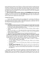
In the netlist above, one needs the subblock statements to know what connections are made
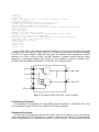
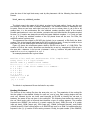
internally to the logic block by local routing. Fig. 1 shows the connections this netlist describes
for the CLB “more_complex.” Note also that while the subblock lines describe the internal
structure of a CLB in terms of BLEs, the BLE structure is general enough that the timing
behaviour of essentially arbitrary logic blocks can be described in terms of subblock lines.
EX-VPR needs the subblock information in a netlist only for timing analysis.
Fig. 1: Connections within logic block “more_complex”
Architecture File Format
An architecture file describes the target FPGA device architecture. Architecture files have
been described in detail in D28, where the DUTYS tool was presented.
Placement File Format
The first line of the placement file lists the netlist (.net) and architecture (.arch) files used to
create this placement. This information is used to ensure you are warned if you accidentally
route this placement with a different architecture or netlist file later. The second line of the file
gives the size of the logic block array used by this placement. All the following lines have the
format:
block_name x y subblock_number
The block name is the name of this block, as given in the input netlist. X and y are the row
and column in which the block is placed, respectively. The subblock number is meaningful only
for pads. Since we can have more than one pad in a row or column when io_rat is set to be
greater than 1 in the architecture file, the subblock number specifies which of the several
possible pad locations in row x and column y contains this pad. Note that the first pads occupied
at some (x, y) location are always those with the lowest subblock numbers --i.e. if only one pad
at (x, y) is used, the subblock number of the I/O placed there will be zero. For CLBs, the
subblock number is always zero.
The placement files output by EX-VPR also include (as a comment) a fifth field: the block
number. This is the internal index used by EX-VPR to identify a block --it may be useful to know
this index if you are modifying EX-VPR and trying to debug something.
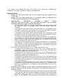
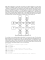
Figure 10 shows the coordinate system used by EX-VPR via a small 2 x 2 CLB FPGA. The
number of CLBs in the x and y directions are denoted by nx and ny, respectively. CLBs all go in
the area with x between 1 and nx and y between 1 and ny, inclusive. All pads either have x
equal to 0 or nx +1 or y equal to 0 or ny + 1.
An example placement file is given below.
Netlist file: xor5.net Architecture file: sample.arch
Array size: 2 x 2 logic blocks
#block name x y subblk block number
#---------- -- -- ------ -----------a 0 1 0 #0 -- NB: block number is a comment.
b 1 0 0 #1
c 0 2 1 #2
d 1 3 0 #3
e 1 3 1 #4
out:xor5 0 2 0 #5
xor5 1 2 0 #6
[1] 1 1 0 #7
The blocks in a placement file can be listed in any order.
Routing File Format
The first line of the routing file gives the array size, nx x ny. The remainder of the routing file
lists the global or the detailed routing for each net, one by one. Each routing begins with the
word net, followed by the net index used internally by EX-VPR to identify the net and, in
brackets, the name of the net given in the netlist file. The following lines define the routing of
the net. Each begins with a keyword that identifies a type of routing segment. The possible
keywords are SOURCE (the source of a certain output pin class), SINK (the sink of a certain
input pin class), OPIN (output pin), IPIN (input pin), CHANX (horizontal channel), and CHANY
(vertical channel). Each routing begins on a SOURCE and ends on a SINK. In brackets after the
keyword is the (x, y) location of this routing resource. Finally, the pad number (if the SOURCE,
SINK, IPIN or OPIN was on an I/O pad), pin number (if the IPIN or OPIN was on a CLB), class
number (if the SOURCE or SINK was on a CLB) or track number (for CHANX or CHANY) is listed
--whichever one is appropriate. The meaning of these numbers should be fairly obvious in each
case. If we are attaching to a pad, the pad number given for a resource is the subblock number
defining to which pad at location (x, y) we are attached. See Figure 10 for a diagram of the
coordinate system used by EX-VPR. In a horizontal channel (CHANX) track 0 is the bottommost
track, while in a vertical channel (CHANY) track 0 is the leftmost track. Note that if only global
routing was performed the track number for each of the CHANX and CHANY resources listed in
the routing will be 0, as global routing does not assign tracks to the various nets.
Fig. 2: Coordinate system used by EX-VPR
For an N-pin net, we need N-1 distinct wiring “paths” to connect all the pins. The first wiring
path will always go from a SOURCE to a SINK. The routing segment listed immediately after the
SINK is the part of the existing routing to which the new path attaches. It is important to realize
that the first pin after a SINK is the connection into the already specified routing tree; when
computing routing statistics be sure that you do not count the same segment several times by
ignoring this fact. An example routing for one net is listed below.
Net 5 (xor5)
SOURCE (1,2) Class: 1 # Source for pins of class 1.
OPIN (1,2) Pin: 4
CHANX (1,1) Track: 1
CHANX (2,1) Track: 1
IPIN (2,2) Pin: 0
SINK (2,2) Class: 0 # Sink for pins of class 0 on a CLB.
CHANX (1,1) Track: 1 # Note: Connection to existing routing!
CHANY (1,2) Track: 1
CHANX (2,2) Track: 1
CHANX (1,2) Track: 1
IPIN (1,3) Pad: 1
SINK (1,3) Pad: 1 # This sink is an output pad at (1,3), subblock 1.
Nets which are specified to be global in the netlist file (generally clocks) are not routed.
Instead, a list of the blocks (name and internal index) which this net must connect is printed
out. The location of each block and the class of the pin to which the net must connect at each
block is also printed. For CLBs, the class is simply whatever class was specified for that pin in
the architecture input file. For pads the pinclass is always -1; since pads do not have
logically-equivalent pins, pin classes are not needed. An example listing for a global net is given
below.
Net 146 (pclk): global net connecting:
Block pclk (#146) at (1, 0), pinclass -1.
Block pksi_17_ (#431) at (3, 26), pinclass 2.
Block pksi_185_ (#432) at (5, 48), pinclass 2.
Block n_n2879 (#433) at (49, 23), pinclass 2.
Debugging Aids
After parsing the netlist and architecture files, EX-VPR dumps out an image of its internal
data structures into net.echo and arch.echo. These files can be examined to be sure that
EX-VPR is parsing the input files as you expect. The critical_path.echo file lists details about the
critical path of a circuit, and is very useful for determining why your circuit is so fast or so slow.
Various other data structures can be output if you uncomment the calls to the output routines;
search the code for echo to see the various data that can be dumped.
If the preprocessor flag DEBUG is defined in ex_vpr_types.h, some additional sanity checks
are performed during a run. I normally leave DEBUG on all the time, as it only slows execution
by 1 to 2%. The major sanity checks are always enabled, regardless of the state of DEBUG.
Finally, if VERBOSE is set in ex_pr_types.h, a great deal of intermediate data will be printed to
the screen as EX-VPR runs. If you set verbose, you may want to redirect screen output to a file.
The initial and final placement costs provide useful numbers for regression testing the netlist
parsers and the placer, respectively. I generate and print out a routing serial number to allow
easy regression testing of the router.
Finally, if you need to route an FPGA whose routing architecture cannot be described in
EX-VPR’s architecture description file, don’t despair! The router, graphics, sanity checker, and
statistics routines all work only with a graph that defines all the available routing resources in
the FPGA and the permissible connections between them. If you change the routines that build
this graph (in rr_graph*.c) so that they create a graph describing your FPGA, you should be
able to route your FPGA. If you want to read a text file describing the entire routing resource
graph, call the dump_rr_graph subroutine.
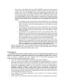
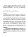
2. EX-VPR GUI
In order to implement a more user-friendly interface than the command line, a GUI was
developed that helps the user input the files and options that were described in subsection 3.1.
The GUI can be seen in Fig. 3. The required fields are the input netlist file in .net format and the
target FPGA architecture file. The produced outputs are the placement and routing files, in the
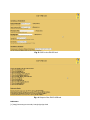
formats described in subsection 3.1.4 in both text and PDF formats (Fig. 4). Also the output
placement and routing can be seen graphically. Additional available outputs are the power
estimation and the critical path details. The specified options are the ones described in
subsection 3.1.3.
Fig. 3: GUI for the EX-VPR tool
Fig. 4: Output of the EX-EX-VPR tool
Reference
[1] http://www.eecg.toronto.edu/~vaughn/vpr/vpr.html