1
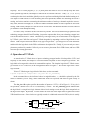
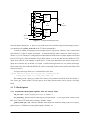
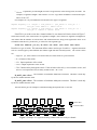
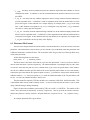
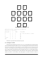
VPR and T-VPack1 User’s Manual (Version 4.30)
Vaughn Betz ([email protected])
March 27, 2000
1 Overview
VPR (Versatile Place and Route) is an FPGA placement and routing tool. VPR has four required and
many optional parameters; it is invoked by typing:
vpr netlist.net architecture.arch placement.p routing.r [-options]
Netlist.net is the netlist describing the circuit to be placed and/or routed, while architecture.arch
describes the architecture of the FPGA in which the circuit is to be realized. If VPR is placing a circuit, the
final placement will be written to placement.p; if VPR is routing a previously placed circuit, the placement
is read from placement.p. The final routing of a circuit is written to file routing.r. The format of each of
these files is described in Section 6.
VPR can be run in one of two basic modes. In its default mode, VPR places a circuit on an FPGA and
then repeatedly attempts to route it in order to find the minimum number of tracks required by the specified
FPGA architecture to route this circuit. If a routing is unsuccessful, VPR increases the number of tracks in
each routing channel and tries again; if a routing is successful, VPR decreases the number of tracks before
trying to route it again. Once the minimum number of tracks required to route the circuit is found, VPR
exits. The other mode of VPR is invoked when a user specifies a specific channel width for routing. In
this case, VPR places a circuit and attempts to route it only once, with the specified channel width. If the
circuit will not route at the specified channel width, VPR simply report that it is unroutable.
VPR can perform either global routing or combined global and detailed routing.
T-VPack is a packing program which can be used with or without VPR. It takes a technology-mapped
netlist (in blif format) consisting of lookup tables (LUTs) and flip flops (FFs) and packs the LUTs and FFs
together to form more coarse-grained logic blocks. The netlist it outputs is in the .net format required by
VPR, and hence can be fed directly into VPR. Its usage is:
t-vpack input.blif output.net [-options]
Typing either VPR or T-VPack with no parameters will print out a list of all the available command
line parameters.
2 Compiling VPR and T-VPack
If your compiler of choice is gcc and you are running a Solaris-based Sparcstation, you can compile
VPR simply by typing make in the directory containing VPR’s source code and makefile. If your compiler
and/or architecture are different, however, you will have to make some small modifications to the make-
1. T-VPack is a timing-driven version of the VPack program that was provided with earlier versions of VPR. When
run in its non-timing-driven mode, T-VPack is equivalent to VPack.
VPR and T-VPack User’s Manual (Version 4.30)
March 27, 2000
1
file. First, change the CC = gcc line in the makefile so that CC is set to the name of your desired compiler.
Second, you may want to change the line OPT_FLAGS = -O3 to set OPT_FLAGS to the value that gives
the highest level of optimization with your compiler, and it may be necessary to give the linker different
options so it finds all the relevant libraries on your machine. If, during compilation, you get an error that
type XPointer is not defined, uncomment the “typedef char *XPointer” line in graphics.c (many X Windows implementations do not define the XPointer type). Finally, if you are compiling VPR on a system
without X Windows (e.g. Windows NT), you should add a “#define NO_GRAPHICS” line to the top of
vpr_types.h. VPR’s built-in graphics will all be removed by this define, allowing compilation on non-X11
machines.
If you are using T-VPack to convert SIS output to VPR’s netlist format, you should make similar
modifications to T-VPack’s makefile.
3 Typical CAD Flow
Figure 1 illustrates the CAD flow we typically use. First, the SIS [1] synthesis package is used to perform technology-independent logic optimization of each circuit. Next, each circuit is technology-mapped
into 4-LUTs and flip flops by FlowMap [2]. The output of FlowMap is a .blif format netlist of LUTs and
Circuit
Logic Optimization (SIS)
Technology Map to LUTs (FlowMap)
.blif Format Netlist of LUTs and
Flip Flops
Logic
Block
Parameters
T-VPack: Pack FFs and LUTs into Logic Blocks
FPGA
Architecture
Description File
.net Format Netlist of Logic
Blocks
VPR:
Place Circuit or Read in an Existing Placement
Existing Placement
or Placement from
Another CAD Tool
Perform Either Global or Combined Global /
Detailed Routing
Placement and Routing Output Files,
Placement and Routing Statistics
Figure 1: CAD flow.
VPR and T-VPack User’s Manual (Version 4.30)
March 27, 2000
2
flip flops. Our T-VPack program [3, 4, 5, 6] then packs this netlist of 4-LUTs and flip flops into more
coarse-grained logic blocks, and outputs a netlist in the .net format VPR uses. VPR [3, 4, 7, 8, 9, 10, 11]
can then place the circuit and either globally route it or perform combined global and detailed routing on it.
The output of VPR consists of a file describing the circuit placement, another file describing the circuit’s
routing, and various statistics concerning the minimum number of tracks per channel required to successfully route, the total wirelength, etc. In order to find the minimum number of tracks required for successful
routing, VPR actually attempts to route the circuit several times with different numbers of tracks allowed
per channel in each attempted routing.
Of course, many variations on this CAD flow are possible. One can use different logic optimizers and
technology mappers than SIS and FlowMap; just put the output netlist from your technology-mapper into
.blif format and feed it into T-VPack. Alternatively, if the logic block you are interested in is not supported
by T-VPack, your CAD flow can bypass T-VPack altogether by outputting a netlist of logic blocks in .net
format. VPR can place and route netlists of any type of logic block -- you simply have to create the netlist
and describe the logic block in the FPGA architecture description file. Finally, if you want only to route a
placement produced by another CAD tool you can create a placement file in VPR format, and have VPR
route this pre-existing placement.
4 Operation of T-VPack
As stated earlier, T-VPack takes as input a technology-mapped netlist of lookup tables (LUTs) and
flip flops in .blif format, and outputs a .net format netlist composed of more complex logic blocks. The
logic block to be targeted is selected via command-line options. The simplest logic block T-VPack can target consists of a LUT and a FF, in the configuration shown in Figure 2. We call this logic block a basic
logic element.
To have T-VPack target a logic block of this form, use the command:
t-vpack <input.blif> <output.net> -lut_size <K> -no_clustering
In the command above, the italicized values in angled brackets, <>, should be replaced by the file
names or numbers you are using, while unitalicized words are keywords and must be typed exactly as
shown.
The -lut_size <K> option specifies the number of inputs to a LUT (i.e. K in Figure 2). If -lut_size is
not specified, a default LUT size of 4 is assumed by T-VPack. The -no_clustering option indicates that
the logic block is a single basic logic element with no local routing to route the logic block output back to
the logic block inputs. By default, T-VPack marks all clock nets in the input netlist as global nets which
VPR should not route. Since clocks are typically routed via a dedicated network in FPGAs, this is usually
Inputs
K-input
LUT
D FF
Out
Clock
Figure 2: Basic logic element.
VPR and T-VPack User’s Manual (Version 4.30)
March 27, 2000
3
BLE
#1
...
I
...
N
N
BLEs
N
Outputs
BLE
#N
I
Inputs
Clock
Figure 3: A cluster-based logic block.
the most realistic thing to do. If, however, you want clocks to be routed as using normal routing resources,
you should specify -global_clocks off on the T-VPack command line.
T-VPack is capable of targeting a more complex form of logic block, which we call a cluster-based
logic block [5]. Figure 3 depicts an example. A cluster-based logic block consists of N basic logic elements (i.e. N LUTs and N FFs), along with local interconnect that allows the N cluster outputs to be routed
back to LUT inputs. Since the number of logic block inputs, I, can be less than the total number of LUT
inputs (KN, where K is the number of inputs per LUT), the local interconnect also allows each of the I
inputs to be routed to any of the KN LUT inputs. Cluster-based logic blocks are very similar to the logic
blocks used in the Altera 8K and 10K FPGAs, and are reasonably similar to those used in the Xilinx 5200
and Virtex FPGAs.
To target such a logic block, use a command line of the form:
t-vpack input.blif output.net -lut_size <K> -cluster_size <N>
-inputs_per_cluster <I> -clocks_per_cluster <C>
The meaning of the -inputs_per_cluster and -cluster_size parameters should be clear from Figure 3.
The -clocks_per_cluster option is used to specify how many distinct clocks can be used by each logic
block.
4.1 T-VPack Options
4.1.1 Architecture Description Options That Are Always Valid
-lut_size <int>: Number of inputs per LUT (i.e. K). Default: 4.
-no_clustering: Specifies that no clustering is to be performed -- i.e. the logic block consists of one
BLE (a LUT and a FF) with no local routing. Default: cluster.
-global_clocks {on | off}: Indicates whether clocks should be marked as being routed via a special,
global resource. VPR does not route global signals. Default: on.
VPR and T-VPack User’s Manual (Version 4.30)
March 27, 2000
4
4.2 Architecture Options Valid Only When -no_clustering Is Not Specified
-cluster_size <int>: Number of BLEs in a cluster-based logic block (i.e. N). Default: 1.
-inputs_per_cluster <int>: Number of distinct inputs in a logic cluster (i.e. I). Default: lut_size *
cluster_size.
-clocks_per_cluster <int>: Number of distinct clocks in a logic cluster. Default: 1.
-muxes_to_cluster_output_pins {on | off}: If “off”, each BLE output is hooked directly to a cluster
output pin. If “on”, a set of N (one per cluster output) N:1 multiplexers allows each output pin to be driven
by any of the N BLEs within a cluster. Default: off.
4.3 CAD Optimization Options
-timing_driven {on | off}: Controls whether the clustering algorithm attempts to optimize circuit
timing by attempting to capture critical connections within a logic cluster. Default: on.
-connection_driven {on | off}: Controls whether or not T-VPack attempts to absorb, within one cluster, connections from the output of one BLE to the input of another. Default: off.
-hill_climbing {on | off}: Controls whether the algorithm used to pack BLEs into clusters allows hill
climbing or is strictly greedy. Default: on.
-cluster_seed {timing | max_inputs}: Specifies the way in which the cluster packing algorithm picks
the first BLE to be placed in an empty cluster. Max_inputs picks the BLE with the most used inputs, while
timing picks the BLE on the most critical path. Default: timing if timing_driven is on, max_inputs otherwise.
-allow_unrelated_clustering {on | off}: Controls whether or not BLEs with no attraction to the current cluster can be packed into it. Default: on.
-alpha <float>: A tradeoff parameter that controls the optimization of delay in packing vs. the optimization of signal sharing. A value of 0 focuses solely on signal sharing, while a value of 1 focuses solely
on timing. This option is meaningful only when timing_driven is on. Default: 0.75.
-recompute_timing_after <int>: T-VPack will recompute its estimate of how timing-critical each
connection is after packing the specified number of BLEs into clusters. This option is meaningful only
when timing_driven is on. Default: 32 000.
-block_delay <float>:
The relative delay of a BLE.
This option is meaningful only when
timing_driven is on. Default: 0.1.
-intra_cluster_net_delay <float>: The relative delay of a signal that goes from one BLE to another
using the local routing within a cluster. This option is meaningful only when timing_driven is on. Default:
0.1.
-inter_cluster_net_delay <float>: The relative delay of a signal that goes from one BLE to another
BLE that is in a different cluster, or an IO pad. This option is meaningful only when timing_driven is on.
Default: 1.0.
-allow_early_exit {on | off}: If on, the clusterer will stop re-timing analyzing a circuit once it
believes the current, partially complete packing, has fixed (“locked”) the critical path. Default: off.
VPR and T-VPack User’s Manual (Version 4.30)
March 27, 2000
5
5 Operation of VPR
Invoke VPR by typing:
vpr input.net input.arch placement.p output.routing [-options]
This section outlines how VPR’s graphics and options work; Section 6 describes the format of each of
the four files used by VPR.
5.1 Graphics
The graphics included in VPR are very easy to use. Click any mouse button on the arrow keys to pan
the view, or click on the Zoom-In, Zoom-Out and Zoom-Fit keys to zoom the view. Click on the Window
button, then on the diagonally opposite corners of a box, to zoom in on a particular area. Selecting PostScript creates a PostScript file (in pic1.ps, pic2.ps, etc.) of the image on screen. Proceed tells VPR to continue with the next step in placing and routing the circuit, while Exit aborts the program. The menu buttons
will be greyed out to show they are not selectable when VPR is working, rather than interactively displaying graphics.
The Toggle Nets button toggles the nets in the circuit visible/invisible. When a placement is being
displayed, routing information is not yet known so nets are simply drawn as a “star;” that is, a straight line
is drawn from the net source to each of its sinks. Click on any clb in the display, and it will be highlighted
in green, while its fanin and fanout are highlighted in blue and red, respectively. Once a circuit has been
routed the true path of each net will be shown. Again, you can click on Toggle Nets to make net routings
visible or invisible, and clicking on a clb or pad will highlight their fanins and fanouts.
When a routing is on-screen, clicking on Toggle RR will switch between various views of the routing
resources available in the FPGA. Wiring segments and clb pins are drawn in black, connections from wiring segments to input pins are shown in blue, connections from output pins to wiring segments are shown
in red, and connections between wiring segments are shown in green. The points at which wiring segments
connect to clb pins (connection box switches) are marked with an “X”. Switch box connections will have
buffers (triangles) or pass transistors (circles) drawn on top of them, depending on the type of switch each
connection uses. Clicking on a clb or pad will overlay the routing of all nets connected to that block on top
of the drawing of the FPGA routing resources, and will label each of the pins on that block with its pin
number. The routing resource view can be very useful in ensuring that you have correctly described your
FPGA in the architecture description file -- if you see switches where they shouldn’t be or pins on the
wrong side of a clb, your architecture description needs to be revised.
When a routing is shown on-screen, clicking on the Congestion button will show any overused routing resources (wires or pins) in red, if any overused resources exist. Finally, when a routing is on screen
you can click on the Crit. Path button to see each of the nets on the critical path in turn. The current net on
the critical path is highlighted in cyan; its source block is shown in yellow and the critical sink is shown in
green.
VPR and T-VPack User’s Manual (Version 4.30)
March 27, 2000
6
5.2 Command-Line Options
To get a list of all the available options type vpr with no parameters.
VPR has a lot of options. The four options most people will be interested in are -fast, -inner_num, route_chan_width, and -route_type. In general for the other options the defaults are fine, and only people looking at how different CAD algorithms perform will try many of them. To understand what the more
esoteric placer and router options actually do, buy [3] or download [7, 8, 9, 10] from the author’s web page
(http://www.eecg.toronto.edu/~vaughn).
In the following text, values in angle brackets, e.g. <int>, should be replaced by the appropriate filename or number. Values in curly braces separated by vertical bars, e.g. {on | off}, indicate all the permissible choices for an option.
5.2.1 General Options
-fast: Sets various placer and router parameters so that a circuit will be placed and routed more
quickly, at the cost of some (~10 - 15%) degradation in quality. Note: -fast should probably not be used
with the timing-driven router, as it can degrade the circuit speed by over 30%, without significantly speeding the router.
-nodisp: Disables all graphics. Useful if you're not running X Windows. Default: graphics enabled.
-auto <int>: Can be 0, 1, or 2. This sets how often you must click Proceed to continue execution after
viewing the graphics. The higher the number, the more infrequently the program will pause. Default: 1.
-route_only: Take an existing placement from the placement file specified on the command line and
route it. Default: off.
-place_only: Place the circuit, but do not route it. Default: off.
-timing_analysis_only_with_net_delay <float>: Do not place or route the circuit; just assume the
delay of every net has the specified value (in seconds), and perform a timing analysis of the circuit. Nets
marked as .global in the netlist still have a zero delay (normally these are just clocks); every other net is
assumed to have the specified delay.
-aspect_ratio <float>: Specifies the aspect ratio (number of columns / number of rows) of an FPGA.
Default 1 (square FPGA).
-nx <int>: Number of columns in the FPGA logic array. Default: set to minimum required to fit circuit.
-ny <int>: Number of rows in the FPGA logic array. Default: set to minimum required to fit circuit.
-full_stats: Print out some extra statistics about the circuit and its routing useful for wireability analysis. Default: off.
-timing_analysis { on | off }: Turn timing analysis of the routing on or off. If it is off, you don’t have
to specify the various timing analysis parameters in the architecture file. Default: on.
VPR and T-VPack User’s Manual (Version 4.30)
March 27, 2000
7
5.2.2 Placer Options
By default, the automatic annealing schedule [3, 9] is used. This schedule gathers statistics as the
placement progresses, and uses them to determine how to update the temperature, when to exit, etc. This
schedule is generally superior to any user-specified schedule. If any of init_t, exit_t or alpha_t is specified,
the user schedule, with a fixed initial temperature, final temperature and temperature update factor is used.
-seed <int>: Sets the initial random seed used by the placer. Default: 1.
-inner_num <float>: The number of moves attempted at each temperature is inner_num times the
total number of blocks4/3 in the circuit. The number of blocks in a circuit is the number of pads plus the
number of clbs. Changing inner_num is the best way to change the speed/quality tradeoff of the placer, as
it leaves the highly-efficient automatic annealing schedule on and simply changes the number of moves per
temperature. Default: 10. Note: specifying -inner_num 1 will speed up the placer by a factor of 10 while
typically reducing placement quality only by 10% or less (depends on the architecture). Hence users more
concerned with CPU time than quality may find this a more appropriate value of inner_num.
-init_t <float>: The starting temperature of the anneal for the manual annealing schedule. Default:
100.
-exit_t <float>: The (manual) anneal will terminate when the temperature drops below the exit temperature. Default: 0.01.
-alpha_t <float>: The temperature is updated by multiplying the old temperature by alpha_t when the
manual annealing schedule is enabled. Default: 0.8.
-fix_pins {random | <file.pads>}: Do not allow the placer to move the I/O locations about during the
anneal. Instead, lock each I/O pad to some location at the start of the anneal. If -fix_pins random is specified, each I/O block is locked to a random pad location to model the effect of poor board-level I/O constraints. If any word other than random is specified after -fix_pins, that string is taken to be the name of a
file listing the desired location of each I/O block in the netlist (i.e. -fix_pins <file.pads>). This pad location file is in the same format as a normal placement file, but only specifies the locations of I/O pads, rather
than the locations of all blocks. Default: off (i.e. placer chooses pad locations).
-place_algorithm {bounding_box | net_timing_driven | path_timing_driven}: Controls the algorithm used by the placer. Bounding_box focuses purely on minimizing the bounding box wirelength of the
circuit, while path_timing_driven focuses on minimizing both wirelength and the critical path delay.
Net_timing_driven is similar to path_timing_driven, but assumes that all nets have the same delay when
estimating the critical path during placement, rather than using the current placement to obtain delay estimates. Default: path_timing_driven.
-place_cost_type {linear | nonlinear}: Select the (wirelength portion of the) placement cost function.
For FPGAs in which all channels have the same width the linear cost function reduces to a bounding box
wirelength cost function. The nonlinear cost function, on the other hand, considers both wirelength and
congestion during placement. Default: linear.
VPR and T-VPack User’s Manual (Version 4.30)
March 27, 2000
8
-place_cost_exp <float>: Only relevant for FPGAs in which the channel width varies from channel
to channel. Sets the exponent (α) used in the linear cost function to penalize routing in narrow channels.
Default: 1.
-place_chan_width <int>: Can be used with the nonlinear cost function to tell VPR how many tracks
a channel of relative width 1 is expected to need to complete routing of this circuit. VPR will then place the
circuit only once, and repeatedly try routing the circuit as usual. If place_chan_width is not specified and
the nonlinear cost is used, VPR will replace and reroute the circuit for each channel width at which it
attempts to map the circuit.
-num_regions <int>: Used only with the nonlinear cost function. VPR will compute congestion on
an array of num_regions X num_regions subareas. Large values of num_regions greatly slow the placer.
Default: 4.
-enable_timing_computations {on | off}: Controls whether or not the placement algorithm prints
estimates of the circuit speed of the placement it generates. This setting affects statistics output only, not
optimization behaviour. Default: on if timing-driven placement is specified, off otherwise.
-block_dist <int>: Specifies that the placement algorithm should print out an estimate of the circuit
critical path, assuming that each inter-block connection is between blocks a (horizontal) distance of
block_dist logic blocks apart. This setting affects statistics output only, not optimization behaviour.
Default: 1. (Currently the code that prints out this lower bound is #ifdef’ed out in place.c -- #define
PRINT_LOWER_BOUND in place.c to reactivate it.)
5.2.3 Placement Options Valid Only With Timing-Driven Placement
-timing_tradeoff <float>: Controls the trade-off between bounding box minimization and delay
minimization in the placer. A value of 0 makes the placer focus completely on bounding box (wirelength)
minimization, while a value of 1 makes the placer focus completely on timing optimization. Default: 0.5.
-recompute_crit_iter <int>: Controls how many temperature updates occur before the placer performs a timing analysis to update its estimate of the criticality of each connection. Default: 1.
-inner_loop_recompute_divider <int>: Controls how many times the placer performs a timing
analysis to update its criticality estimates while at a single temperature. Default: 0.
-td_place_exp_first <float>: Controls how critical a connection is considered as a function of its
slack, at the start of the anneal. If this value is 0, all connections are considered equally critical. If this
value is large, connections with small slacks are considered much more critical than connections with
small slacks. As the anneal progresses, the exponent used in the criticality computation gradually changes
from its starting value of td_place_exp_first to its final value of td_place_exp_last. Default: 1.
-td_place_exp_last <float>: Controls how critical a connection is considered as a function of its
slack, at the end of the anneal. See discussion for -td_place_exp_first, above. Default: 8.
5.2.4 Router Options
-route_type {global | detailed}: Specifies whether global routing or combined global and detailed
routing should be performed. Default: detailed (i.e. combined global and detailed routing).
VPR and T-VPack User’s Manual (Version 4.30)
March 27, 2000
9
-route_chan_width <int>: Tells VPR to route the circuit with a certain channel width. No binary
search on channel capacity will be performed to find the minimum number of tracks required for routing -VPR simply reports whether or not the circuit will route at this channel width.
-router_algorithm {breadth_first | timing_driven}: Selects which router algorithm to use. The
breadth-first router focuses solely on routing a design successfully, while the timing-driven router focuses
both on achieving a successful route and achieving good circuit speed. The breadth-first router is capable
of routing a design using slightly fewer tracks than the timing-driving router (typically 5% if the timingdriven router uses its default parameters; this can be reduced to about 2% if the router parameters are set so
the timing-driven router pays more attention to routability and less to area). The designs produced by the
timing-driven router are much faster, however, (2x - 10x) and it uses less CPU time to route. Default:
timing_driven.
-max_router_iterations <int>: The number of iterations of a Pathfinder-based router that will be
executed before a circuit is declared unrouteable (if it hasn’t routed successfully yet) at a given channel
width. Default: 30. Speed-quality trade-off: reduce this number to speed up the router, at the cost of some
increase in final track count. This is most effective if -initial_pres_fac is simultaneously increased.
-initial_pres_fac <float>: Sets the starting value of the present overuse penalty factor. Default: 0.5.
Speed-quality trade-off: increase this number to speed up the router, at the cost of some increase in final
track count. Values of 1000 or so are perfectly reasonable.
-first_iter_pres_fac <float>: Similar to -initial_pres_fac. This sets the present overuse penalty factor for the very first routing iteration. -initial_pres_fac sets it for the second iteration. Default: 0.5.
-pres_fac_mult <float>: Sets the growth factor by which the present overuse penalty factor is multiplied after each router iteration. Default: 2.
-acc_fac <float>: Specifies the accumulated overuse factor (historical congestion cost factor).
Default: 1.
-bb_factor <int>: Sets the distance (in channels) outside of the bounding box of its pins a route can
go. Larger numbers slow the router somewhat, but allow for a more exhaustive search of possible routes.
Default: 3.
-base_cost_type [demand_only | delay_normalized | intrinsic_delay]: Sets the basic cost of using
a routing node (resource). Demand_only sets the basic cost of a node according to how much demand is
expected for that type of node. Delay_normalized is similar, but normalizes all these basic costs to be of
the same magnitude as the typical delay through a routing resource. Intrinsic_delay sets the basic cost of a
node to its intrinsic delay. Default: delay_normalized for the timing-driven router and demand_only for
the breadth-first router.
-bend_cost <float>: The cost of a bend. Larger numbers will lead to routes with fewer bends, at the
cost of some increase in track count. If only global routing is being performed, routes with fewer bends
will be easier for a detailed router to subsequently route onto a segmented routing architecture. Default: 1
if global routing is being performed, 0 if combined global/detailed routing is being performed.
VPR and T-VPack User’s Manual (Version 4.30)
March 27, 2000
10
5.2.5 Routing Options Valid Only for Timing-Driven Routing
-astar_fac <float>: Sets how aggressive the directed search used by the timing-driven router is. Values between 1 and 2 are reasonable, with higher values trading some quality for reduced CPU time.
Default: 1.2.
-max_criticality <float>: Sets the maximum fraction of routing cost that can come from delay (vs.
coming from routability) for any net. A value of 0 means no attention is paid to delay; a value of 1 means
nets on the critical path pay no attention to congestion. Default: 0.99.
-criticality_exp <float>: Controls the delay - routability tradeoff for nets as a function of their slack.
If this value is 0, all nets are treated the same, regardless of their slack. If it is very large, only nets on the
critical path will be routed with attention paid to delay. Other values produce more moderate tradeoffs.
Default: 1.
6 File Formats
In all the file format that follow, a sharp (#) character anywhere in a line indicates that the rest of the
line is a comment, while a backslash (\) at the end of a line (and not in a comment) means that this line is
continued on the line below.
6.1 Circuit Netlist (.net) Format
Three different circuit elements are available: input pads, output pads, and logic blocks, and are specified using the keywords .input, .output, and .clb, respectively. The format is shown below.
element_type_keyword blockname
pinlist: net_a net_b net_c ...
subblock: subblock_name pin_num1 pin_num2 ...
# Only needed if a clb
A circuit element is created by specifying a keyword at the start of a line, followed by the name to be
used to identify this block. The line immediately below this keyword line starts with the identifier pinlist:
and then lists the names of the nets connected to each pin of the logic block or pad. Input and output pads
(.inputs and .outputs) have only one pin, while logic blocks (.clbs) have as many pins as the architecture
file used for this run of VPR specifies. The first net listed in the pinlist connects to pin 0 of a clb, and so on.
If some pin of a clb is to be left unconnected, the corresponding entry in the pinlist should specify the
reserved word open instead of a net name.
Logic blocks (.clbs) also have to specify the internal contents of the logic block with subblock lines.
Each clb must have at least one subblock line, and can have up to subblocks_per_clb subblock lines, where
subblocks_per_clb is set in the architecture file. A clb may have less than subblocks_per_clb subblock
lines, since some of the subblocks in the clb may be unused. Each subblock is a BLE -- a K-input LUT
(where K is set via the subblock_lut_size line in the architecture description file) and a flip flop, as shown
in Figure 2. The subblock line first gives the name of the subblock, and then gives the clb pin or a subblock output pin within this logic block to which each BLE pin is connected. If a BLE pin is unconnected,
the corresponding pin entry should be set to the keyword open.
The order of the BLE pins is:
subblock_lut_size LUT input pins, the BLE output, and the clock input (subblock_lut_size + 2 pins total).
VPR and T-VPack User’s Manual (Version 4.30)
March 27, 2000
11
Each of the subblock LUT input pins can be connected to any of the clb (logic block) input pins, or to
the output of any of the subblocks in this logic block. A connection to a clb input pin is specified by giving
the number of the clb pin in the appropriate place, while a connection to a subblock output is specified by
“ble_<subblock_number>”. For example, to connect to clb pin 0, one lists 0 in the appropriate place,
while to connect to the output of subblock 0, one lists ble_0 in the appropriate place. Each subblock clock
pin can similarly be connected to either a clb input pin or the output of a subblock in the same logic block.
If the subblock clock pin is “open” the BLE output is the unregistered LUT output; otherwise the BLE output is assumed to be registered. The entry corresponding to the subblock output pin specifies the number
of the clb output pin to which it connects, or open if this subblock output is doesn’t connect to any clb output pin (which happens when a subblock output is used only locally, within a logic block).
The only other keyword is .global. Use .global lines to specify that a net or nets should not be considered by the placement cost function or routed. It is assumed that some global routing resources exist to
route these very high fanout signals (generally clocks). The syntax of the .global statement is:
.global net_a net_b ...
An example netlist in which the logic block is a single BLE is given below.
#This netlist describes a small circuit with two inputs
#and one output. There is only one clb block, which is
#a 3-input BLE (LUT+FF) that has one unconnected input.
#This netlist assumes that the architecture input file defines
#a clb as a 3-input BLE with pins 0, 1, and 2 being the LUT inputs,
#pin 3 being the LUT output, and pin 4 being the BLE clock.
.input a
pinlist: a
#Input pad.
#Blocks can have the same name as nets with no conflict.
.input bpad
pinlist: b
.clb simple
# Logic block.
pinlist: a b open and2 open
subblock: sb_one 0 1 open 3 open
.output out_and2
pinlist: and2
# 2 LUT inputs used, clock input unconnected.
# Subblock line says the same thing.
#Output pad.
In the netlist above the subblock line adds no new information -- since the logic block only contains
one BLE, which pins are hooked to this BLE is obvious. Consider a netlist in which each logic block is a
cluster-based logic block containing two subblocks, or BLEs, however.
.input a
pinlist: a
.input bpad
pinlist: b
.input c
pinlist: c
.input clk
pinlist: clk
VPR and T-VPack User’s Manual (Version 4.30)
March 27, 2000
12
a
b
c
pin 0
pin 4
out_1
pin 1
pin 2
pin 5
out_2
pin 3
clk
pin 6
Figure 4: Connections within logic block “more_complex” specified by subblock lines of netlist above.
.global clk
#
#
#
#
#
# Typical case: clock needn’t be routed, as there’s a
# special network for it.
Example logic block: 4 inputs, 2 outputs, 1 clock.
Internally, the logic block contains two BLEs,
each of which consists of a 3-LUT and a FF.
Local routing allows subblock outputs to connect to subblock inputs in the same
logic block.
.clb more_complex
pinlist: a b c open out_1 out_2 clk
subblock: sb_zero 0 1 open 4 open
#
#
subblock: sb_one ble_0 1 2 5 6
#
#
#
BLE inputs are a and b, output
goes to out_1. Output isn’t registered.
BLE inputs are the output of subblock 0,
and nets b and c. The output goes to out_2.
The output is registered.
.output opad_1
pinlist: out_1
.output opad_2
pinlist: out_2
In the netlist above, one needs the subblock statements to know what connections are made internally
to the logic block by local routing. Figure 4 shows the connections this netlist describes for the clb
“more_complex.” Note also that while the subblock lines describe the internal structure of a clb in terms
of BLEs, the BLE structure is general enough that the timing behaviour of essentially arbitrary logic blocks
can be described in terms of subblock lines. VPR needs the subblock information in a netlist only for timing analysis.
6.2 FPGA Architecture File (.arch) Format
Each line in an architecture file consists of a keyword followed by one or more parameters. In the
description below, strings between curly braces, {}, denote all the possible choices for an option. All of the
following keywords must be specified in the architecture file.
VPR and T-VPack User’s Manual (Version 4.30)
March 27, 2000
13
io_rat <int>: Sets the number of pads (inputs or outputs) that fit into the space occupied by one clb.
This is the number of pads in each row or column of the FPGA.
6.2.1 Description of Relative Channel Widths in the FPGA
The next three keywords are used to describe the relative widths of the various channels in the FPGA.
If global routing is to be performed, channels in different directions and in different parts of the FPGA can
be set to different relative widths. If detailed routing is to be performed, however, all the channels in the
FPGA must have the same width.
chan_width_io <float>: Width of the channels between the pads and core relative to the widest core
channel.
chan_width_x {gaussian | uniform | pulse | delta} <peak> <width> <xpeak> <dc>: The italicized
quantities are needed only for pulse, gaussian, and delta (which doesn’t need width). Most values are from
0 to 1. Sets the distribution of tracks for the x-directed channels -- the channels that run horizontally.
If uniform is specified, you simply specify one argument, peak. This value (by convention between 0
and 1) sets the width of the x-directed core channels relative to the y-directed channels and the channels
between the pads and core. Figure 5 should make the specification of uniform (dashed line) and pulse
(solid line) channel widths more clear. The gaussian keyword takes the same four parameters as the pulse
keyword, and they are all interpreted in exactly the same manner except that in the gaussian case width is
the standard deviation of the function.
The delta function is used to specify a channel width distribution in which all the channels have the
same width except one. The syntax is chan_width_x delta peak xpeak dc. Peak is the extra width of the single wide channel. Xpeak is between 0 and 1 and specifies the location within the FPGA of the extra-wide
channel -- it is the fractional distance across the FPGA at which this extra-wide channel lies. Finally, dc
specifies the width of all the other channels. For example, the statement chan_width_x delta 3 0.5 1 specifies that the horizontal channel in the middle of the FPGA is four times as wide as the other channels.
chan_width_y {gaussian | uniform | pulse | delta} peak <width> <xpeak> <dc>: Sets the distribution of tracks for the y-directed channels.
xpeak is pulse midpoint
1.
pulse
width
Relative
Channel
Width
uniform 0.5
peak
dc
0.
Fractional Distance across FPGA
1.
Figure 5: Specification of relative channel widths.
VPR and T-VPack User’s Manual (Version 4.30)
March 27, 2000
14
6.2.2 Logic Block Description
inpin class: <int> [global] {top | bottom | left | right} {top | bottom | left | right} ...: Declares an
input pin, determines the class to which this pin belongs, and sets the side(s) of CLBs on which the physical output pin connection(s) is (are). All pins with the same class number are logically equivalent -- such as
all the inputs of a LUT. Class numbers must start at zero and be consecutive. The global keyword is
optional; if specified, it comes after the class number. Global input pins can connect only to signals
marked as global in the netlist (typically clocks). Global input pins are not connected into the normal routing; it is assumed they connect to a special, dedicate resource used for special nets like clocks.
outpin class: <int> {top | bottom | left | right} {top | bottom | left | right} ...: All parameters have
the same meanings as their counterparts in the inpin statement.
NOTE: The order in which your inpin and outpin statements appear must be the same as the order in
which your netlist (.net) file lists the connections to the clbs. For example, if the first pin on each clb in the
netlist file is the clock pin, your first pin statement in the architecture file must be an inpin statement defining the clock pin.
Pads are always assumed to have only one pin (either an input or an output), and this pin is accessible
from the one channel bordering that pad. Hence no inpin or outpin statements are given for pads.
subblocks_per_clb <int>: Specifies the maximum number of subblocks, or BLEs, in each logic
block. This information is used only for timing analysis.
subblock_lut_size <int>: The number of LUT inputs to each of the subblock BLEs (i.e. K). Again,
this information is only needed for timing analysis. Even if your logic block is not constructed from BLEs,
it is possible to describe the timing relations between inputs and outputs in terms of BLEs, as one of the
examples below illustrates.
The listing below is for an FPGA with all channels of the same width, and a clb compatible with that
produced by T-VPack with the -no_clustering option. This clb contains a 4-input LUT and a flip flop; the
input pins are listed first, followed by the clb output pin, followed by the clock pin. Notice that the four
inputs all have the same pin class, indicating that they are logically equivalent and the router may connect
nets to any one of them. Notice also that pins can be physically accessible from several sides.
# Uniform channel architecture, 4-input LUT and a FF (one BLE) per clb.
io_rat 2
chan_width_io 1
chan_width_x uniform 1
chan_width_y uniform 1
#2 Pads per row or column.
#Same as core channels.
#All same width
# 4-input LUT. LUT inputs first, then output, then clock.
inpin class: 0 bottom top
#Physical pins at both top and bottom of clb.
inpin class: 0 left right
inpin class: 0 bottom top
inpin class: 0 left right
outpin class: 1 top bottom
inpin class: 2 top
# Clock pin
# Class 0 is LUT inputs, class 1 is the output, class 2 is the clock
VPR and T-VPack User’s Manual (Version 4.30)
March 27, 2000
15
# in this case.
subblocks_per_clb 1
subblock_lut_size 4
# One BLE in each logic block
# The LUT in a BLE has 4 inputs
As a second example of an architecture file, consider a logic block consisting of a cluster-based logic
block, where each logic block has 5 inputs for use by its BLEs, 2 outputs and one clock input. Each logic
block contains two separate BLEs, and each BLE consists of a 4-input LUT and a flip flop. If the .net file
was created with T-VPack, the pin ordering we need to match the .net file is: inputs for use by BLEs, outputs, clock.
# Uniform channel architecture, cluster-based logic block containing
# 2 BLEs.
io_rat 2
chan_width_io 1
chan_width_x uniform 1
chan_width_y uniform 1
# Logic block with 2 BLEs.
# outputs, then the clock.
#2 Pads per row or column.
#Same as core channels.
#All same width
5 Inputs for use by BLEs first, then two
inpin class: 0 bottom
inpin class: 0 left
inpin class: 0 right
inpin class: 0 top
inpin class: 0 bottom
outpin class: 1 top bottom
outpin class: 1 left right
inpin class: 2 global top
#Output 1
#Output 2
#Clock -> accessible only by global nets in this case
# Class 0 is LUT inputs, class 1 is the output, class 2 is the clock
# in this case.
subblocks_per_clb 2
subblock_lut_size 4
# Two BLEs in each logic block
# The LUT in a BLE has 4 inputs
Notice that all the inputs are of the same class, indicating they are all logically equivalent, and all the
outputs are of the same class, indicating they are also logically equivalent. This is true of all cluster-based
logic blocks, as the local routing within the block provides full connectivity. However, for most logic
blocks all the inputs and all the outputs are not logically equivalent. For example, consider the logic block
in Figure 6, which consists of a 3-input and gate and a 2-input or gate. In this case, the set {in1, in2, in3}
is logically equivalent, and could all be made class 0. Similarly, the set {in4, in5} is logically equivalent,
and could be made class 1. Out1 and out2 are obviously not logically equivalent, so each must be a different class, say class 2 and class 3.
VPR and T-VPack User’s Manual (Version 4.30)
March 27, 2000
16
in1
in2
in3
out1
in4
out2
in5
Figure 6: Example logic block where many pins are not logically equivalent.
inpin class: 0
inpin class: 0
inpin class: 0
inpin class: 1
inpin class: 1
outpin class: 2
outpin class: 3
top
left
right
bottom
right
left
top
#in1
#in2
#in3
#in4
#in5
#out1
#out2
If we want to perform timing analysis on the logic block of Figure 6, we must describe the timing relationship between the inputs and outputs. Clearly out1 depends only on in1, in2 and in3, while out2
depends only on in4 and in5. Therefore we could model this logic block as consisting of two BLEs, with
each BLE having 3 inputs.
subblocks_per_clb 2
subblock_lut_size 3
One line of a .net file of a circuit made out of such logic blocks might therefore be:
.clb block_1
pinlist: in1 in2 in3 in4 in5 out1 out2
subblock: and_gate 0 1 2 5 open
# out1 depends on in1, in2 and in3,
# and is not registered.
subblock: or_gate 3 4 open 6 open
# out2 depends on in4 and in5
# and is not registered.
6.2.3 Detailed Routing Architecture Description
The following information is only required to be in the architecture description file if combined global/detailed routing is to be performed. Note that currently combined global/detailed routing is possible
only when all channels have been specified to have the same width.
switch_block_type {subset | wilton | universal}: All the switch blocks [12] have Fs = 3. That is,
whenever horizontal and vertical channels intersect, each wire segment can connect to three other wire
segments. The exact topology of which wire segment connects to which can be one of three choices. The
subset switch box is the planar or domain-based switch box used in the Xilinx 4000 FPGAs -- a wire segment in track 0 can only connect to other wire segments in track 0 and so on. The wilton switch box is
described in [13], while the universal switch box is described in [14]. To see the topology of a switch box,
simply hit the “Toggle RR” button when a completed routing is on screen in VPR. In general the wilton
switch box is the best of these three topologies and leads to the most routable FPGAs.
VPR and T-VPack User’s Manual (Version 4.30)
March 27, 2000
17
Fc_type {absolute | fractional}: Indicates whether the three Fc [12] values (see below) should be
interpreted as the number of tracks to which each pin connects (absolute), or the fraction of tracks in a
channel to which each pin connects (fractional).
Fc_input <float>: Sets the number of tracks to which each logic block input pin connects in each
channel bordering the pin. The Fc value used is always the minimum of the specified Fc and the channel
width, W, so you can set Fc to be huge if you want Fc to always be W.
Fc_output <float>: Sets the number of tracks to which each logic block output pin connects in each
channel bordering the pin.
Fc_pad <float>: Sets the number of tracks to which each I/O pad connects in the channel bordering
the pad.
segment frequency: <float> length: <int | longline> wire_switch: <int> opin_switch: <int>
Frac_cb: <float> Frac_sb: <float> Rmetal: <float> Cmetal: <float>
Describes a type of segment. You can specify as many types of segments as you like -- just use one segment line for each. The meaning of each value is:
• frequency: The fraction (from 0 to 1) of routing tracks composed of this type of segment. The sum
of the frequency values for all the segment lines must be 1 -- i. e. 100% of the tracks have been
described.
• length: Either the number of logic blocks spanned by each segment, or the keyword longline. Longline means segments of this type span the entire FPGA array.
• wire_switch: The index of the switch type used by other wiring segments to drive this type of segment. That is, switches going to this segment from other pieces of wiring will use this type of
switch.
• opin_switch: The index of the switch type used by clb and pad output pins to drive this type of segment.
• Frac_cb: Describes the internal population of the segment for connection boxes (connections to
logic blocks). This number gives the fraction (from 0 to 1) of logic blocks passed by this segment
to which it will have a connection box. A switch exists from a segment to a logic block pin only if
(1) the segment wants a connection box to that logic block and (2) the logic block connection box
pattern for that pin wants a connection to that segment.
• Frac_sb: Describes the internal population of the segment for switch boxes (connections to other
routing tracks). This number gives the fraction (from 0 to 1) of the length + 1 switch blocks which
could exist along the segment that do in fact exist. So, a segment of length 9 that had a Frac_sb
value of 0.5 would have 5 switch boxes along its length. Exactly which tracks a segment connects
to at each switch box is determined by the switch_box_type parameter.
• Rmetal: Resistance per unit length (in terms of logic blocks) of this wiring track, in Ohms. For
example, a segment of length 5 with Rmetal = 10 Ohms / logic block would have an end-to-end
resistance of 50 Ohms.
VPR and T-VPack User’s Manual (Version 4.30)
March 27, 2000
18
• Cmetal: Capacitance per unit length (in terms of logic blocks) of this wiring track, in Farads. For
example, a segment of length 5 with Cmetal = 2e-14 F / logic block would have a total metal capacitance of 10e-13F.
For example, let’s say an architecture file describes two types of segments.
segment frequency: 0.5 length: 2 wire_switch: 0 opin_switch: 0
Frac_sb: 0.666 Rmetal: 5 Cmetal: 5e-15
segment frequency: 0.5 length: 4 wire_switch: 0 opin_switch: 0
Frac_sb: 1. Rmetal: 3 Cmetal: 2e-15
Frac_cb: 1. \
Frac_cb: 0.5 \
If the FPGA you wish to route has a channel width of 4, one channel will look as shown in Figure 7.
Notice that 2 tracks (50% of the tracks) are segments of length 2, and 2 tracks are segments of length four.
Also notice that the number of switch boxes and connection boxes along each segment has been set in
accordance with the Frac_sb and Frac_cb values for each segment type.
switch <int> buffered: { yes | no } R: <float> Cin: <float> Cout: <float> Tdel: <float>
Describes a a type of switch. This statement defines what a certain type of switch is -- segment statements
refer to a switch types by their number (the number right after the switch keyword). The various values
are:
• buffered: yes, if this switch is a tri-state buffer, no if this switch is a pass transistor.
• R: resistance of the switch.
• Cin: Input capacitance of the switch.
• Cout: Output capacitance of the switch.
• Tdel: Intrinsic delay through the switch. If this switch was driven by a zero resistance source, and
drove a zero capacitance load, its delay would be Tdel + R * Cout.
R_minW_nmos <float>: The resistance of minimum-width nmos transistor. This data is used only
by the area model built into VPR.
R_minW_pmos <float>: The resistance of minimum-width pmos transistor. This data is used only
by the area model built into VPR.
The lines below give an example of a detailed routing description from a .arch file.
Switch Box
Connection Box
Figure 7: Example of a segmented routing channel with four tracks per channel.
VPR and T-VPack User’s Manual (Version 4.30)
March 27, 2000
19
switch_block_type planar
Fc_type fractional
# Uses the fewest switches on a segmented architecture.
# Fc values below are in terms of fraction of W.
Fc_output 1.
# clb output pins connect to all W tracks in adjacent channels
# (if each of those tracks wants a connection box there).
Fc_input
0.5
# clb input pins connect to half (0.5 * W) of adjacent tracks
# (if each of those tracks wants a connection box there).
Fc_pad
0.7
# I/O pads connect to 70% (0.7 * W) of adjacent tracks
# (if each of those tracks wants a connection box there).
#
#
#
#
50% of segments are length 2, 50% are length 4. Length two segments are driven by
type 1 switches when the connection is coming from another wire, and are driven
by type 0 switches when the connection comes from a clb output pin.
The length four segments are always driven by type 0 switches.
segment frequency: 0.5 length: 2 wire_switch: 1 opin_switch: 0 Frac_cb: 1. \
Frac_sb: 0.666 Rmetal: 5 Cmetal: 5e-15
segment frequency: 0.5 length: 4 Frac_cb: 0.5 Frac_sb: 1. Rmetal: 3 \
Cmetal: 2e-15
# In this case, type 1 switches are pass transistors, while type 0 switches are
# tri-state buffers.
switch 1
switch 0
buffered: no R: 100 Cin: 2e-15 Cout: 2e-15 Tdel: 0
# Pass transistor
buffered: yes R: 50 Cin: .5e-15 Cout: 4e-15 Tdel: 1e-11 # Tri-state buffer
R_minW_nmos 100
R_minW_pmos 200
# Used by area model.
Min-width transistor resistances.
6.2.4 Timing Analysis Parameters
The following parameters are required if timing analysis is to be performed on the placed and routed
circuit, or the timing-driven router is to be used.
C_ipin_cblock <float>: Input capacitance of the buffer isolating a routing track from the connection
boxes (multiplexers) that select the signal to be connected to an logic block input pin. One of these buffers
is inserted in the FPGA for each track at each location at which it connects to a connection box. For example, a routing segment that spans three logic blocks, and connects to logic blocks at two of these three possible locations would have two isolation buffers attached to it. If a routing track connects to the logic
blocks both above and below it at some point, only one isolation buffer is inserted at that point. If your
connection from routing track to connection block does not include a buffer, set this parameter to the
capacitive loading a track would see at each point where it connects to a logic block or blocks.
T_ipin_cblock <float>: Delay to go from a routing track, through the isolation buffer (if your architecture contains these) and a connection block (typically a multiplexer) to a logic block input pin.
T_ipad <float>: Delay through an input pad.
T_opad <float>: Delay through an output pad.
VPR and T-VPack User’s Manual (Version 4.30)
March 27, 2000
20
Logic Block
Connection
Block
Routing Track
Isolation Buffer
Figure 8: Routing track to logic block connection structure.
T_clb_ipin_to_sblk_ipin <float>: Delay from an input pin of a clb (logic block) to an input pin of a
subblock within that clb. For architectures without local routing (i.e. clb input pins connect directly to
some logic element, like a LUT or multiplexer) this delay is essentially zero.
T_sblk_opin_to_sblk_ipin <float>: Delay from the output of a subblock to the input of another subblock within the same clb. For architectures without local routing (e.g. the output of one subblock is hardwired to the input of another) this delay is essentially zero.
T_sblk_opin_to_clb_opin <float>: Delay from the output of a subblock to a clb (logic block) output
pin. For architectures without local routing (e.g. the output of a LUT is hardwired to each logic block output), this delay is essentially zero.
T_subblock T_comb: <float> T_seq_in: <float> T_seq_out: <float>
Describes the delays within a subblock. There must be one T_subblock line for each subblock a logic
block can contain -- i.e. there must be subblocks_per_clb of these T_subblock lines. The first line specifies
the delays of subblock zero, which is the first subblock listed in each clb in the circuit netlist file. The second T_subblock line specifies the delay of subblock one, (the second subblock in each clb in the circuit
netlist file), and so on. If the subblocks within a clb have different delays then, you must list them in the
same order in the architecture and netlist files.
T_sblk_opin_to_sblk_ipin
Subblock
0
CLB
Outputs
CLB
Inputs
Subblock
1
T_sblk_opin_to_clb_opin
T_clb_ipin_to_sblk_ipin
Figure 9: Local routing delays within a logic block (CLB).
VPR and T-VPack User’s Manual (Version 4.30)
March 27, 2000
21
• T_comb: The delay from any subblock input to the subblock output when this subblock is used in
combinational mode. A subblock is used in combinational mode when the netlist leaves its clock
pin OPEN.
• T_seq_in: The delay from any subblock input pin to the FF storage element when this subblock is
used in sequential mode. A subblock is used in sequential mode when the netlist hooks its clock
pin to some signal. If this subblock was a simple flip flop, for example, then T_seq_in is the setup
time. If this subblock corresponds to, say, a LUT feeding into a flip flop, then T_seq_in should be
set to the LUT delay plus the setup time.
• T_seq_out: The delay from the subblock storage element (FF) to the subblock output pin when this
block is used in sequential mode. A subblock is used in sequential mode when the netlist hooks its
clock pin to some signal. If this subblock had a flip flop hooked to its output pin, for example, then
T_seq_out would be the clock-to-Q delay of the flip flop.
6.3 Placement File Format:
The first line of the placement file lists the netlist (.net) and architecture (.arch) files used to create this
placement. This information is used to ensure you are warned if you accidentally route this placement with
a different architecture or netlist file later. The second line of the file gives the size of the logic block array
used by this placement.
All the following lines have the format:
block_name
x
y subblock_number
The block name is the name of this block, as given in the input netlist. X and y are the row and column in which the block is placed, respectively. The subblock number is meaningful only for pads. Since
we can have more than one pad in a row or column when io_rat is set to be greater than 1 in the architecture file, the subblock number specifies which of the several possible pad locations in row x and column y
contains this pad. Note that the first pads occupied at some (x, y) location are always those with the lowest
subblock numbers -- i.e. if only one pad at (x, y) is used, the subblock number of the I/O placed there will
be zero. For clbs, the subblock number is always zero.
The placement files output by VPR also include (as a comment) a fifth field: the block number. This
is the internal index used by VPR to identify a block -- it may be useful to know this index if you are modifying VPR and trying to debug something.
Figure 10 shows the coordinate system used by VPR via a small 2 x 2 clb FPGA. The number of clbs
in the x and y directions are denoted by nx and ny, respectively. Clbs all go in the area with x between 1
and nx and y between 1 and ny, inclusive. All pads either have x equal to 0 or nx + 1 or y equal to 0 or ny +
1.
An example placement file is given below.
VPR and T-VPack User’s Manual (Version 4.30)
March 27, 2000
22
Pad
(0,2)
Chany
(0,2)
Pad
(1,3)
Pad
(2,3)
Chanx
(1,2)
Chanx
(2,2)
Clb
(1,2)
Chany
(1,2)
Chanx
(1,1)
Pad
(0,1)
Chany
(0,1)
Clb
(1,1)
Clb
(2,2)
Chany
(2,2)
Pad
(3,2)
Chany
(2,1)
Pad
(3,1)
Chanx
(2,1)
Chany
(1,1)
Clb
(2,1)
Chanx
(1,0)
Chanx
(2,0)
Pad
(1,0)
Pad
(2,0)
Figure 10: Coordinate system used by VPR.
Netlist file: xor5.net
Architecture file: sample.arch
Array size: 2 x 2 logic blocks
#block name
#---------a
b
c
d
e
out:xor5
xor5
[1]
x
-0
1
0
1
1
0
1
1
y
-1
0
2
3
3
2
2
1
subblk
-----0
0
1
0
1
0
0
0
block number
-----------#0 -- NB: block number is a comment.
#1
#2
#3
#4
#5
#6
#7
The blocks in a placement file can be listed in any order.
6.4 Routing File Format
The first line of the routing file gives the array size, nx x ny. The remainder of the routing file lists the
global or the detailed routing for each net, one by one. Each routing begins with the word net, followed by
the net index used internally by VPR to identify the net and, in brackets, the name of the net given in the
netlist file. The following lines define the routing of the net. Each begins with a keyword that identifies a
type of routing segment. The possible keywords are SOURCE (the source of a certain output pin class),
SINK (the sink of a certain input pin class), OPIN (output pin), IPIN (input pin), CHANX (horizontal
channel), and CHANY (vertical channel). Each routing begins on a SOURCE and ends on a SINK. In
VPR and T-VPack User’s Manual (Version 4.30)
March 27, 2000
23
brackets after the keyword is the (x, y) location of this routing resource. Finally, the pad number (if the
SOURCE, SINK, IPIN or OPIN was on an I/O pad), pin number (if the IPIN or OPIN was on a clb), class
number (if the SOURCE or SINK was on a clb) or track number (for CHANX or CHANY) is listed -whichever one is appropriate. The meaning of these numbers should be fairly obvious in each case. If we
are attaching to a pad, the pad number given for a resource is the subblock number defining to which pad at
location (x, y) we are attached. See Figure 10 for a diagram of the coordinate system used by VPR. In a
horizontal channel (CHANX) track 0 is the bottommost track, while in a vertical channel (CHANY) track
0 is the leftmost track. Note that if only global routing was performed the track number for each of the
CHANX and CHANY resources listed in the routing will be 0, as global routing does not assign tracks to
the various nets.
For an N-pin net, we need N-1 distinct wiring “paths” to connect all the pins. The first wiring path
will always go from a SOURCE to a SINK. The routing segment listed immediately after the SINK is the
part of the existing routing to which the new path attaches. It is important to realize that the first pin after
a SINK is the connection into the already specified routing tree; when computing routing statistics be sure
that you do not count the same segment several times by ignoring this fact. An example routing for one net
is listed below.
Net 5 (xor5)
SOURCE
OPIN
CHANX
CHANX
IPIN
SINK
CHANX
CHANY
CHANX
CHANX
IPIN
SINK
(1,2)
(1,2)
(1,1)
(2,1)
(2,2)
(2,2)
(1,1)
(1,2)
(2,2)
(1,2)
(1,3)
(1,3)
Class:
Pin: 4
Track:
Track:
Pin: 0
Class:
Track:
Track:
Track:
Track:
Pad: 1
Pad: 1
1
# Source for pins of class 1.
1
1
0
1
1
1
1
# Sink for pins of class 0 on a clb.
# Note: Connection to existing routing!
# This sink is an output pad at (1,3), subblock 1.
Nets which are specified to be global in the netlist file (generally clocks) are not routed. Instead, a list
of the blocks (name and internal index) which this net must connect is printed out. The location of each
block and the class of the pin to which the net must connect at each block is also printed. For clbs, the class
is simply whatever class was specified for that pin in the architecture input file. For pads the pinclass is
always -1; since pads do not have logically-equivalent pins, pin classes are not needed. An example listing
for a global net is given below.
Net 146 (pclk): global net connecting:
Block pclk (#146) at (1, 0), pinclass -1.
Block pksi_17_ (#431) at (3, 26), pinclass 2.
Block pksi_185_ (#432) at (5, 48), pinclass 2.
Block n_n2879 (#433) at (49, 23), pinclass 2.
VPR and T-VPack User’s Manual (Version 4.30)
March 27, 2000
24
7 Debugging Aids
After parsing the netlist and architecture files, VPR dumps out an image of its internal data structures
into net.echo and arch.echo. These files can be examined to be sure that VPR is parsing the input files as
you expect. The critical_path.echo file lists details about the critical path of a circuit, and is very useful for
determining why your circuit is so fast or so slow. Various other data structures can be output if you
uncomment the calls to the output routines; search the code for echo to see the various data that can be
dumped.
If the preprocessor flag DEBUG is defined in vpr_types.h, some additional sanity checks are performed during a run. I normally leave DEBUG on all the time, as it only slows execution by 1 to 2%. The
major sanity checks are always enabled, regardless of the state of DEBUG. Finally, if VERBOSE is set in
vpr_types.h, a great deal of intermediate data will be printed to the screen as VPR runs. If you set verbose,
you may want to redirect screen output to a file.
The initial and final placement costs provide useful numbers for regression testing the netlist parsers
and the placer, respectively. I generate and print out a routing serial number to allow easy regression testing of the router.
Finally, if you need to route an FPGA whose routing architecture cannot be described in VPR’s architecture description file, don’t despair! The router, graphics, sanity checker, and statistics routines all work
only with a graph that defines all the available routing resources in the FPGA and the permissible connections between them. If you change the routines that build this graph (in rr_graph*.c) so that they create a
graph describing your FPGA, you should be able to route your FPGA. If you want to read a text file
describing the entire routing resource graph, call the dump_rr_graph subroutine.
8 References
[1]
E. M. Sentovich et al, “SIS: A System for Sequential Circuit Analysis,” Tech. Report No. UCB/ERL
M92/41, University of California, Berkeley, 1992.
[2]
J. Cong and Y. Ding, “FlowMap: An Optimal Technology Mapping Algorithm for Delay Optimization in Lookup-Table Based FPGA Designs,” IEEE Trans. CAD, Jan. 1994, pp. 1 - 12.
[3]
V. Betz, J. Rose and A. Marquardt, Architecture and CAD for Deep-Submicron FPGAs, Kluwer
Academic Publishers, 1999.
[4]
V. Betz, “Architecture and CAD for the Speed and Area Optimization of FPGAs,” Ph.D. Dissertation, University of Toronto, 1998.
[5]
V. Betz and J. Rose, “Cluster-Based Logic Blocks for FPGAs: Area-Efficiency vs. Input Sharing
and Size,” CICC, 1997, pp. 551 - 554.
[6]
A. Marquardt, V. Betz and J. Rose, “Using Cluster-Based Logic Blocks and Timing-Driven Packing
to Improve FPGA Speed and Density,” ACM/SIGDA Int. Symp. on FPGAs, 1999, pp. 37 - 46.
[7]
V. Betz and J. Rose, “Directional Bias and Non-Uniformity in FPGA Global Routing Architectures,” ICCAD, 1996, pp. 652 - 659.
[8]
V. Betz and J. Rose, “On Biased and Non-Uniform Global Routing Architectures and CAD Tools for
FPGAs,” CSRI Technical Report #358, Department of Electrical and Computer Engineering, Uni-
VPR and T-VPack User’s Manual (Version 4.30)
March 27, 2000
25
versity of Toronto, 1996. (Available for download from http://www.eecg.toronto.edu/~vaughn/
papers/techrep.ps.Z).
[9]
V. Betz and J. Rose, “VPR: A New Packing, Placement and Routing Tool for FPGA Research,”
Seventh International Workshop on Field-Programmable Logic and Applications, 1997, pp. 213 222.
[10] A. Marquardt, V. Betz and J. Rose, “Timing-Driven Placement for FPGAs,” ACM/SIGDA Int. Symp.
on FPGAs, 2000, pp. 203 - 213.
[11]
V. Betz and J. Rose, “Automatic Generation of FPGA Routing Architectures from High-Level
Descriptions,” ACM/SIGDA Int. Symp. on FPGAs, 2000, pp. 175 - 184.
[12] S. Brown, R. Francis, J. Rose, and Z. Vranesic, Field-Programmable Gate Arrays, Kluwer Academic Publishers, 1992.
[13] S. Wilton, “Architectures and Algorithms for Field-Programmable Gate Arrays with Embedded
Memories,” Ph.D. Dissertation, University of Toronto, 1997. (Available for download from http://
www.ee.ubc.ca/~stevew/publications.html).
[14] Y. W. Chang, D. F. Wong, and C. K. Wong, “Universal Switch Modules for FPGA Design,” ACM
Trans. on Design Automation of Electronic Systems, Jan. 1996, pp. 80 - 101.
VPR and T-VPack User’s Manual (Version 4.30)
March 27, 2000
26