1
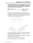
PCI - PIO
RoHS Compliant
PCI Digital Input/Output Card
User Guide
Document Reference
Document Issue Level
Product User Guide
1.2
PCI-PIO
Table of Contents
Table of Contents
Introduction........................................................................................................................................ 3
Copyright.......................................................................................................................................3
Limitations of Liability................................................................................................................. 3
Trademarks.................................................................................................................................... 3
About The Manual............................................................................................................................. 4
Overview............................................................................................................................................ 5
Chapter 1............................................................................................................................................ 6
Technical Specification................................................................................................................. 6
Chapter 2............................................................................................................................................ 7
Installing the PCI-PIO................................................................................................................... 7
Chapter 3............................................................................................................................................ 8
Connection Details........................................................................................................................ 8
Suitable Interface Signal Types.....................................................................................................9
Chapter 4.......................................................................................................................................... 10
Address Map................................................................................................................................11
i8255 PIO................................................................................................................................12
i8254 Counter / Timer............................................................................................................ 13
Counter / Timer Modes ..........................................................................................................14
Counter Control...................................................................................................................... 15
Interrupt Selection.................................................................................................................. 17
Chapter 5.......................................................................................................................................... 19
Electromagnetic Compatibility (EMC)....................................................................................... 19
EMC Specification..................................................................................................................20
Chapter 6.......................................................................................................................................... 21
Amendment History......................................................................................................................... 22
Contact Details............................................................................................................................ 22
Page 2 of 23
PCI-PIO
Introduction
Introduction
Copyright
All rights reserved. No part of this publication may be reproduced, stored in any retrieval system, or transmitted, in
any form or by any means, electronic, mechanical, photocopied, recorded or otherwise, without the prior
permission, in writing, from the publisher. For permission in the UK please contact Blue Chip Technology.
Information offered in this manual is believed to be correct at the time of printing. Blue Chip Technology accepts
no responsibility for any inaccuracies. The information contained herein is subject to change without notice.
There are no express or implied licences granted herein to any intellectual property rights of Blue Chip Technology
Ltd.
Limitations of Liability
In no event shall Blue Chip Technology be held liable for any loss, expenses or damages of any kind whatsoever,
whether direct, indirect, incidental or consequential, arising from the design or use of this product or the support
materials supplied with this product. If this product proves to be defective, Blue Chip Technology is only obliged to
replace or refund the purchase price at Blue Chip Technology's discretion according to their Terms and Conditions
of Sale.
Trademarks
All trademarks and registered names acknowledged.
IBM, PC, AT and PS/2 are trademarks of International Business Machines Corporation (IBM).
AMI is a registered trademark of American Megatrends Inc.
MSDOS and WINDOWS are registered trademarks of the Microsoft Corporation.
Page 3 of 23
PCI-PIO
About The Manual
About The Manual
This manual is organised into six chapters. Each chapter covers a different aspect of using the
PCI-PIO. In order to get the best results from the product, the user is urged to read all chapters,
paying particular note to Chapter 2 which deals with the initial installation of the card.
Overview
Provides a brief introduction to the card
Chapter 1
Presents the card’s technical specification. Use this section to determine the card’s
suitability for a particular application
Chapter 2
Explains how to install the card in your computer.
Chapter 3
Details the connections to and from the card
Chapter 4
Gives details of the card’s address mapping and internal register details allowing
the user to write custom software to control the card.
Chapter 5
Electromagnetic Compatibility
Chapter 6
Shows typical Input and Output circuitry
This manual describes the complete hardware functionality of the PCI-PIO board. All the
functions may not necessarily be supported by the current release of the driver.
Page 4 of 23
PCI-PIO
Product Overview
Overview
The PCI-PIO is a RoHS-compliant PCI-compatible half-card which provides digital input/outputs
and counter/timers.
There are 48 TTL-compatible programmable digital input/outputs available from the board. If the
controlling devices are used in handshake mode, the handshake lines are available as interrupt
sources.
There are also three programmable counter/timers, the enable and clock inputs being available
externally, if required , and the outputs being accessible externally or as interrupt sources. A
4MHz crystal oscillator is available on board to allow the counter/timers to act as accurate
timebases.
All input/output lines are available at an industry standard 50 way D-type plug connector.
One PCI interrupt line may be selectively driven by the seven interrupt sources on the board, the
interrupting source being readily identified by the board.
The PCI-PIO is intended to be installed with the minimum of user interaction. The board is
configured by the system BIOS and by the application drivers and no on-board links are required
to select functionality.
Page 5 of 23
PCI-PIO
Technical Specification
Chapter 1
Technical Specification
Number Of I/O Channels
48 arranged as 2 x 3 x 8 I/O bits
Signal Levels
5 Volt TTL Logic levels
Outputs:
Logic Low Level:
Logic High Level:
0 Volts (min) – 0.4 Volts (max) @ IOL = 2.5 mA
3.5 Volts (min) – 5 Volts (max) @ IOH = -400µA
Drive Current:
2.5 mA. (Logic Low) Vout = 0.4 Volts
-400 µA (Logic High) Vout = 3.5 Volts
Input Loading:
-10 µA (Logic Low)
+10 µA (Logic High)
Counter/Timers:
3 x 16 Bit.
Counter/timers 0, 1 and 2 may be cascaded to provide
a single 48 bit Counter/timer
All Counter/timers may be clocked externally at a maximum
rate of 4 MHz
On board Oscillator:
Frequency 4Mhz
4 PIO handshake control Lines
Interrupt Sources:
Register selectable to 3 Counter/timer outputs
and 4 PIO handshake control lines
Interrupt Levels Supported:
All PCI interrupts
Address Overhead
16 contiguous addresses in 16 byte block
Board Power Requirement:
1.6W
This board requires both 5V and 3V3 power lines but it will
operate with Vio of either 3.3V or 5V
Temperature:
Non Operating:
Operating:
-20 °C to 70 °C
0 °C to 70 °C
MTBF:
500,000 hours (Bellcore method)
Signal Connections:
1 x 50 way male “D-type” plug
Dimensions
125 (L) x 91 (H) board only
135 (L) x 122 (H) x 22 (W) including bracket
Chapter 1
Page 6 of 23
PCI-PIO
Installation
Chapter 2
Installing the PCI-PIO
The card is installed by removing the cover of the host computer and inserting the card into a free
PCI slot. The rear panel of the card should then be secured to the rear panel of the host computer
with the screw supplied with the computer.
When the computer is switched on, the BIOS will detect the presence of the card and will allocate
it with a base address and an interrupt. These parameters may then be used to configure
application software to access the card.
If the card is to be directly accessed by a user’s application, it will be necessary for the application
to determine where the BIOS has located the card.
One way of determining the Base address of the card can be found by using the “bc_probe” utility
which is supplied on the Blue Chip Support CD, or alternatively can be downloaded from the Blue
Chip website
This program must be run under DOS or a Full Screen session under Windows. It will not operate
in a DOS Window.
The BC_probe utility will return addresses which look like the following
bar1, IO, 0xC800
bar2, IO, 0xC400
The Bar 1 address just sets up address space in memory to be used by the card while the Bar 2
address is the base address for the Registers for the card.
These can be used as follows in conjunction with the Address map on page 12 of this user manual.
Base+0 PIO 1 Port A Input/Output Register R/W >> 0xC400
Base+1 PIO 1 Port B Input/Output Register R/W >> 0xC401
...
Base+F5 Counter Control Register B R/W >> 0xC40F
Chapter 2
Page 7 of 23
PCI-PIO
Connection Details
Chapter 3
Connection Details
The following table refers to the 50 way D-type plug on the rear of the card
PIN
USAGE
PIN
USAGE
PIN
USAGE
1
PIO1 port A, b0 (PAA0)
18
PIO1 port C, b1 (PAC1)
34
2
PIO1 port A, b1 (PAA1)
19
PIO1 port C, b2 (PAC2)
35
3
PIO1 port A, b2 (PAA2)
20
36
4
5
6
7
8
PIO1 port A, b3 (PAA3)
PIO1 port A, b4 (PAA4)
PIO1 port A, b5 (PAA5)
PIO1 port A, b6 (PAA6)
PIO1 port A, b7 (PAA7)
21
22
23
24
25
PIO1 port C, b3 (PAC3)
and/or interrupt source or
Counter I/O
PIO1 port C, b4 (PAC4)
PIO1 port C, b5 (PAC5)
PIO1 port C, b6 (PAC6)
PIO1 port C, b7 (PAC7)
PIO2 port A, b0 (PBA0)
9
10
11
PIO1 port B, b0 (PAB0)
PIO1 port B, b1 (PAB1)
PIO1 port B, b2 (PAB2)
26
27
28
PIO2 port A, b1 (PBA1)
PIO2 port A, b2 (PBA2)
PIO2 port A, b3 (PBA3)
42
43
44
12
13
14
15
16
PIO1 port B, b3 (PAB3)
PIO1 port B, b4 (PAB4)
PIO1 port B, b5 (PAB5)
PIO1 port B, b6 (PAB6)
PIO1 port B, b7 (PAB7)
29
30
31
32
33
PIO2 port A, b4 (PBA4)
PIO2 port A, b5 (PBA5)
PIO2 port A, b6 (PBA6)
PIO2 port A, b7 (PBA7)
PIO2 port B, b0 (PBB0) or
Counter I/O
45
46
47
48
49
PIO2 port B, b4 (PBB4)
PIO2 port B, b5 (PBB5)
PIO2 port B, b6 (PBB6)
PIO2 port B, b7 (PBB7)
PIO2 port C, b0 (PBC0) and/or
interrupt source or Counter I/O
PIO2 port C, b1 (PBC1)
PIO2 port C, b2 (PBC2)
PIO2 port C, b3 (PBC3) and/or
interrupt source or Counter I/O
PIO2 port C, b4 (PBC4)
PIO2 port C, b5 (PBC5)
PIO2 port C, b6 (PBC6)
PIO2 port C, b7 (PBC7)
Digital Ground
17
PIO1 port C, b0 (PAC0)
and/or Interrupt source or
Counter I/O
50
Digital Ground
37
38
39
40
41
PIO2 port B, b1 (PBB1) or
Counter I/O
PIO2 port B, b2 (PBB2) or
Counter I/O
PIO2 port B, b3 (PBB3)
The following diagram shows how the pins on the male D-type connector are numbered
If you are having difficulty in obtaining suitable cables to attach to the PCI-PIO, the Farnell part
numbers for suitable connectors are 1084683 and 4155312.
Chapter 3
Page 8 of 23
PCI-PIO
Connection Details
Suitable Interface Signal Types
The input and output signals for the PCI-PIO parallel ports and counter/timers are strictly digital
TTL levels with voltage limits of zero volts for a logic low and +5 volts for a logic high. Voltages
outside these limits may cause damage to the card. The output current drive capability makes the
card suitable for connection to TTL logic type circuits. The PCI-PIO is compatible with most
types of TTL logic. Because the lines are TTL it is recommended that input signal lines do not
exceed 2 metres in length. Operation at longer lengths may cause drive level problems.
Driving conventional relay coils is not recommended without external protection even if the coil
current required is less than the PCI-PIO can provide. Relay coils are inductive and as such can
generate large flyback voltages when de-energised which will destroy the device outputs.
Chapter 3
Page 9 of 23
PCI-PIO
Programming Details
Chapter 4
This chapter provides brief details of the cards internal registers.
The board’s input/output facilities are provided by two Intel i8255 PIO devices and an Intel
i8254 Counter/timer
Each PIO provides 24 programmable digital I/O channels. It is suitable for sensing the presence
of, or driving TTL connections only. These connections should be kept as short as possible, less
than 2 metres is recommended.
Each PIO appears to the PC as four I/O addressable registers. The first three registers control the
I/O ports which can be set as input or output by writing suitable codes to the fourth Control Port.
Three modes of operation are available within the device:Mode 0 is for general purpose I/O and allows all three ports to be configured as either inputs or
outputs.
Mode 1 is for full duplex parallel communication and allows one port to be configured for inputs,
another for outputs and the third as transfer handshake lines and interrupt sources.
Mode 2 is for half duplex parallel data communication, and allows one port to be configured for
data transfer I/O, a second as transfer handshake lines and an interrupt source, and the third as a
general purpose I/O port (similar to mode 0).
For mode 0, a summary of the codes required to change the operation of the ports are given later.
A typical sequence of events to use this feature would be :
●
Decide on the mix of input/outputs required and write the appropriate code to the Control
Register.
●
Read from the selected input port or write to the selected output port.
The 8254 contains three 16-bit Counter/timers each of which has separate clock and enable inputs
and an output, all of which are TTL compatible. Connections to these signals should be kept as
short as possible, less than 2 metres is recommended.
The 8254 appears to the PC as four ports. The first three are count registers for the three
counter/timers, and the fourth is a Control Register which configures the mode of operation of the
three counters. These are accessed at the addresses shown in the map below.
A summary of the codes required to change the port operations are given later.
Chapter 4
Page 10 of 23
PCI-PIO
Programming Details
Address Map
The address map for the PCI-PIO occupies a 16-byte block of addresses.
All the following addresses are relative to PCI base address register 2, located at address 18 (hex)
in the PCI configuration space.
ADDRESS
Base + 0
Base + 1
Base +2
Base + 3
Base + 4
Base + 5
Base + 6
Base + 7
Base + 8
Base + 9
Base + A
Base + B
Base + C
Base + D
Base + E
Base + F
FUNCTION
PIO 1, Port A Input/Output Register
PIO 1, Port B Input/Output Register
PIO 1, Port C Input/Output Register
PIO 1, Control Register
PIO 2, Port A Input/Output Register
PIO 2, Port B Input/Output Register
PIO 2, Port C Input/Output Register
PIO 2, Control Register
Counter/timer 0 Count Register
Counter/timer 1 Count Register
Counter/timer 2 Count Register
Counter/timer Control Register
Interrupt enable register
Interrupt status register
Counter control register A
Counter control register B
READ/
WRITE
(Channel 0 to 7)
(Channel 8 to 15)
(Channel 16 to 23)
(Channel 24 to 31)
(Channel 32 to 39)
(Channel 40 to 47)
R/W
R/W
R/W
W
R/W
R/W
R/W
W
R/W
R/W
R/W
W
R/W
R
R/W
R/W
The i8255 PIO and i8254 Counter/timer ICs are complex devices. For full details on how to
program these devices, refer to the manufacturer’s data sheets. Presented here is a brief summary
of the main features of each.
Chapter 4
Page 11 of 23
PCI-PIO
Programming Details
i8255 PIO
The PIO chip can operate in one of three modes.
The first (Mode 0) provides for simple inputs and outputs for three, 8-bit ports. Data is written to
or read from a specified port (A, B, or C) without the use of handshaking. The following table
gives a summary of the most commonly used control words which must be written to the control
port to configure the i8255 I/O ports in Mode 0.
CONTROL
WORD (hex)
CONTROL
WORD
(decimal)
SET ALL
of PORT
A as
SET ALL
of PORT
B as
SET HIGH
4 BITS of
C as
SET LOW 4
BITS of C as
80
81
82
83
88
89
8A
8B
90
91
92
93
98
99
9A
9B
128
129
130
131
136
137
138
139
144
145
146
147
152
153
154
155
Output
Output
Output
Output
Output
Output
Output
Output
Input
Input
Input
Input
Input
Input
Input
Input
Output
Output
Input
Input
Output
Output
Input
Input
Output
Output
Input
Input
Output
Output
Input
Input
Output
Output
Output
Output
Input
Input
Input
Input
Output
Output
Output
Output
Input
Input
Input
Input
Output
Input
Output
Input
Output
Input
Output
Input
Output
Input
Output
Input
Output
Input
Output
Input
Mode 1 enables the transfer of data to or from a specified 8 bit port (A or B) in conjunction with
strobes or handshaking signals on port C. These handshaking signals may be used to drive
interrupt channels if required.
In Mode 2, data is transferred via one bi-directional 8 bit port (A) with handshaking (port C).
These handshaking signals may be used to drive interrupt channels if required.
Refer to the i8255 data sheet for full details of the settings and use of Modes 1 and 2.
Chapter 4
Page 12 of 23
PCI-PIO
Programming Details
i8254 Counter / Timer
The counter/timer circuit contains three independent 16-bit counters which may be operated in a
variety of modes. There are five basic modes of operation with each mode providing a different
output signal. Presented here is a brief summary of some of the modes possible by programming
the counter / timer’s internal registers.
All three counter/timers may be operated independently, with separate clocks and enable controls.
Counter 0, Counter 1 and Counter 2 may be connected in series. Counter 0 output to Counter 1
clock input and/or Counter 1 output to Counter 2 clock input, to allow the facility of generating
very long delay periods.
The outputs from any counter/timer may be configured to generate an interrupt when going high
or low, and may also be made accessible on the back panel connector.
The clock and enable inputs of the counter/timers may also be made accessible on the back panel
connector.
Chapter 4
Page 13 of 23
PCI-PIO
Programming Details
Counter / Timer Modes
The following modes of operation exist by programming the control register within the i8254.
N.B. The interrupts may be generated when the Counter/timer outputs go low or high, selected by
bits in the counter control registers.
Mode 0
When programmed, the output pin will go LOW. When the counter decrements from the value
loaded into the count registers to zero, the output pin will go HIGH. It will remain high until the
count is re-programmed into the count registers.
Mode 1
When the count registers are programmed the output pin will be HIGH. When a LOW going
signal is applied to the gate input, the count starts and the output will fall LOW, returning HIGH
at the end of the count.
Mode 2
This mode operates as a frequency divider. When programmed the output pin is HIGH. When
the count decrements to a value of 1 the output pin will go LOW for ONE clock cycle only and
then return HIGH. This cycle repeats continuously without the need to re-program the count
value.
Mode 3
When programmed the output pin will toggle each time the count register decrements to its base
level from the value programmed into it. If the count value loaded is an odd number then the
counter will reach zero before the output pin toggles. This mode therefore acts as a frequency
divider with an approximate 1:1 mark-space ratio.
Mode 4
This mode is similar to mode 2 but the output pin pulses when the count reaches zero instead of 1.
Mode 5
This mode is similar to mode 4 except that the count sequence is triggered by the gate line.
Chapter 4
Page 14 of 23
PCI-PIO
Programming Details
Counter Control
The control and output lines of the counter/timer may be accessed on the rear panel connector by
sacrificing some of the digital I/O lines.
The clock inputs of the i8254 counter/timer are selected using the Counter Input Select Register A
at Base + E (Hex), as shown below:-
Bit no.
Counter Input Select Register A (Base + E)
Function
b7
Enable counter outputs such that
b6
Counter 0 interrupt level:-
b5..b4
Counter 2 clock source:-
b3..b2
Counter 1 clock source:-
b1..b0
Counter 0 clock source:-
CISR_A
PBB0 = Counter 2 output
PBB1 = Counter 0 output
PBB2 = Counter 1 output
0 = Interrupt on counter out low
1 = Interrupt on counter out high
00 = 4 MHz oscillator
01 = PBB2 port line
10 = Counter 1 output
11 = PBC0 port line
00 = 4 MHz oscillator
01 = PBB1 port line
10 = Counter 0 output
11 = PAC3 port line
00 = 4 MHz oscillator
01 = PBB0 port line
10 = Counter 2 output
11 = PAC0 port line
If Bit b7 in the counter control register is set, then the counter outputs are enabled onto port lines
PBB0, PBB1 & PBB2, which connect to the 50 way D-type connector. Consequently this port
must be set as an input in the relevant i8255 device to avoid contention. This same condition
applies to any port line which is used for a counter/timer function.
Chapter 4
Page 15 of 23
PCI-PIO
Programming Details
The enable inputs of the i8254 counter are selected using the Counter Input Select Register B at
Base + F (Hex), as shown below:-
Counter Input Select Register B (Base + F)
Bit no.
Function
b7
b6
b5..b4
b3..b2
b1..b0
CISR_B
Counter 2 interrupt level:- 0 = Interrupt on counter out low
1 = Interrupt on counter out high
Counter 1 interrupt level:- 0 = Interrupt on counter out low
1 = Interrupt on counter out high
Counter 2 enable source:- 00 = Permanently enabled
01 = PBB1 port line
10 = PBC0 port line
11 = PBC3 port line
Counter 1 enable source:- 00 = Permanently enabled
01 = PBB0 port line
10 = PAC3 port line
11 = PBC0 port line
Counter 0 enable source:- 00 = Permanently enabled
01 = PBB2 port line
10 = PAC0 port line
11 = PAC3 port line
Notice that it is possible by judicious setting of Counter Input Registers A and B, to set each
timer/counter to operate with an external count input, enable and counter output if required. For
example it is possible to set Counter 0 to use PBB0 as a count input, PBB2 as an enable input,
and PBB1 as a count output. Other combinations are possible, but because of the flexibility
which is permitted, care must be exercised to avoid conflicting uses of the same port lines.
Chapter 4
Page 16 of 23
PCI-PIO
Programming Details
Interrupt Selection
A total of seven sources of interrupt are available from the two PIO devices and the
counter/timers. These interrupts are summarised below:-
• INT1 (AC0) is available when PIO1 is operating in mode 1. It provides a Read Request
interrupt for input operations or a Write Request interrupt for output operations on PIO1
port A (PAA[0:7]).
• INT2 (AC3) is available when PIO1 is operating in mode 1. It provides a Read Request
interrupt for input operations or a Write Request interrupt for output operations on PIO1
port B (PAB[0:7]).
• INT3 (BC0) is available when PIO2 is operating in mode 1. It provides a Read Request
interrupt for input operations or a Write Request interrupt for output operations on PIO2
port A (PBA[0:7]).
• INT4 (BC3) is available when PIO2 is operating in mode 1. It provides a Read Request
interrupt for input operations or a Write Request interrupt for output operations on PIO2
port B (PBB[0:7]).
• INT5 is the output from Counter/timer 0, and may be used to generate interrupts on timed
events.
• INT6 is the output from Counter/timer 1, and may be used to generate interrupts on timed
events.
• INT7 is the output from Counter/timer 2, and may be used to generate interrupts on timed
events.
The use of interrupts is not essential but greatly enhances the functionality of the card.
To enable the generation of an interrupt or a combination of interrupts, an enable word must be
written to the Interrupt Enable Register at Base + C (Hex), as shown below:-
Chapter 4
Page 17 of 23
PCI-PIO
Programming Details
Bit no.
b7
b6
b5
b4
b3
b2
b1
b0
Interrupt Enable Register (Base + C)
Function
IER
Not used
Counter/timer 2 interrupt control
(1 = Enable, 0 = Disable)
Counter/timer 1 interrupt control
(1 = Enable, 0 = Disable)
Counter/timer 0 interrupt control
(1 = Enable, 0 = Disable)
Port BC3 interrupt control (1 = Enable, 0 = Disable)
Port BC0 interrupt control (1 = Enable, 0 = Disable)
Port AC3 interrupt control (1 = Enable, 0 = Disable)
Port AC0 interrupt control (1 = Enable, 0 = Disable)
When an interrupt is recognised by the processor, the source or sources of interrupt may be read
from the Interrupt Status Register at Base + D (Hex), as shown below:-
Bit no.
b7
b6
b5
b4
b3
b2
b1
b0
Interrupt Status Register (Base + D)
Function
ISR
Not used
Counter/timer 2 interrupt occurred
Counter/timer 1 interrupt occurred
Counter/timer 0 interrupt occurred
Port BC3 interrupt control occurred
Port BC0 interrupt control occurred
Port AC3 interrupt control occurred
Port AC0 interrupt control occurred
Having serviced an interrupt, the source may be cleared by momentarily clearing the relevant bit
in the Interrupt Enable Register.
The diagram following demonstrates the various ways in which the counter/timers may be
interconnected and the registers and bits that control them.
Chapter 4
Page 18 of 23
PCI-PIO
Chapter 4
Programming Details
Page 19 of 23
PCI-PIO
Electromagnetic Compatibility
Chapter 5
Electromagnetic Compatibility (EMC)
This product meets the requirements of the European EMC Directive (89/336/EEC) and is eligible to bear the CE
mark.
It has been assessed operating in our standard industrial PC. However, because the board can be installed in a
variety of computers, certain conditions have to be applied to ensure that the compatibility is maintained. It
meets the requirements of EN55022:1995 for a Class A product subject to those conditions.
• The board must be installed in a computer system which provides screening suitable for an industrial
environment.
• Any recommendations made by the computer system manufacturer/supplier must be complied with
regarding earthing and the installation of boards.
• The board must be installed with the backplate securely screwed to the chassis of the computer to ensure
good metal-to-metal (i.e. earth) contact.
• Most EMC problems are caused by the external cabling to boards. It is imperative that any external cabling
to the board is totally screened, and that the screen of the cable connects to the metal end bracket of the
board and hence to earth. It is recommended that round screened cables with a braided wire screen are used
in preference to those with a foil screen and drain wire. Use metal connector shells which connect around
the full circumference of the screen; they are far superior to those which earth the screen by a simple “pigtail”. Standard ribbon cable will not be adequate unless it is contained wholly within the cabinetry housing
the industrial PC.
• Ensure that the screen of the external cable is bonded to a good RF earth at the remote end of the cable.
• Cables which connect externally to boards at TTL levels should not exceed two metres in length.
Failure to observe these recommendations may invalidate the EMC compliance.
Warning
This is a Class A Product. In a domestic environment this product may
cause radio-interference in which case the user may be required to take
adequate measures.
Chapter 5
Page 20 of 23
PCI-PIO
Electromagnetic Compatibility
EMC Specification
A suitably compliant industrial PC fitted with this card meets the requirements of the European
Union Electromagnetic Compatibility Directive 89/336/EEC and its amending Directives, and
specifically the following standards:
Chapter 5
Emissions
EN 55022:1998 Class A
Immunity
EN 55024:1998
Page 21 of 23
PCI-PIO
Timer Example
Chapter 6
Typical Input and Output Connections to the PIOs and the
Counter/Timers
Note that whilst the i8255 port is shown above as an input device, it may also be programmed as
an output device. Under these circumstances the pull-up/down resistor will act as a load.
If using one of the common input pins as an input to the Timer, care must be taken to set the
i8255 port as an input to avoid conflict, otherwise the external input at the pin will be in conflict
with the output of the output port.
Chapter 6
Page 22 of 23
Product Form Factor
History
Amendment History
Issue Level
1.0
1.1
Issue Date
15/01/2007
07/02/2007
Author
Tmck
TMCK
21/03/2007
TMCK
1.2
Amendment Details
Initial Release
Added MTBF figures and minor grammar changes made,
corrected EMC details
Corrected Reversed Drawings
Contact Details
Blue Chip Technology Ltd.
Chowley Oak
Tattenhall
Chester
CH3 9EX
U.K.
Telephone: +44 (0)1829 772000
Facsimile: +44 (0)1829 772001
www.bluechiptechnology.co.uk
Plasma PC Sales
[email protected]
Single Board Computer Sales
[email protected]
Rack mount PC Sales
[email protected]
Data and IO Sales
[email protected]
Technical Support
[email protected]