1
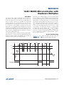
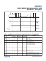
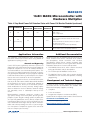
19-6254; Rev 0; 3/12 MAXQ615 16-Bit MAXQ Microcontroller with Hardware Multiplier General Description Features The MAXQ615 is a low-power, 16-bit MAXQM microcontroller designed for low-power applications. The device combines a powerful 16-bit RISC microcontroller and integrated peripherals including multiple high-speed serial communication interfaces and flexible port I/O. High-speed communication interfaces include dual SPI and I2C. The device also provides three instances of the 16-bit timer B peripheral. A 16 x 16 hardware multiply/ accumulate with 48-bit accumulator provides support for computationally intensive applications. The device provides 48KB of flash memory and 2KB of data SRAM. For the ultimate in low-power performance, the device includes an ultra-low-power stop mode (0.2FA typ). In this mode, the minimum amount of circuitry is powered. Wake-up sources include external interrupts, the powerfail interrupt, and a timer interrupt. The microcontroller runs from a single 2.4V to 3.6V power-supply operating voltage. SCore Functionality High-Performance, Low-Power 16-Bit MAXQ20S RISC Core DC to 20MHz Operation Across Entire Operating Range 2.4V to 3.6V Operating Voltage Three Independent Data Pointers Accelerate Data Movement with Automatic Inc/Dec Dedicated Pointer for Direct Read from Code Space 16-Bit Instruction Word, 16-Bit Data Bus 16 x 16-Bit General-Purpose Working Registers Optimized for C Compiler Applications Portable Computing Battery-Powered Portable Equipment Consumer Electronics Home Appliances White Goods SMemory 48KB Flash Memory 1KB Page Sectors 20,000 Erase/Write Cycles per Sector 2KB Data SRAM Masked ROM Available SI/O and Peripherals Power-Fail Warning Power-On Reset/Brownout Reset Three 16-Bit Programmable Timers/Counters with Prescaler Programmable Watchdog Timer Internal 20MHz Clock ±5% Dual SPI Ports with 16-Byte FIFO I2C Communication Port Up to 12 General-Purpose I/O Pins SLow Power Consumption 0.2µA (typ) in Stop Mode 2.6mA (typ) at 20MHz Divided System Clock Modes Available Ordering Information appears at end of data sheet. For related parts and recommended products to use with this part, refer to www.maxim-ic.com/MAXQ615.related. MAXQ is a registered trademark of Maxim Integrated Products, Inc. Note: Some revisions of this device may incorporate deviations from published specifications known as errata. Multiple revisions of any device may be simultaneously available through various sales channels. For information about device errata, go to: www.maxim-ic.com/errata. ����������������������������������������������������������������� Maxim Integrated Products 1 For pricing, delivery, and ordering information, please contact Maxim Direct at 1-888-629-4642, or visit Maxim’s website at www.maxim-ic.com. MAXQ615 16-Bit MAXQ Microcontroller with Hardware Multiplier ABSOLUTE MAXIMUM RATINGS (All voltages relative to GND.) Voltage Range on VDD..........................................-0.3V to +3.6V Voltage Range on Any Lead..................... -0.3V to (VDD + 0.5V) Continuous Output Current Any Single I/O Pin...........................................................32mA All I/O Pins Combined......................................................32mA Continuous Power Dissipation (TA = +70NC) TQFN (derate 16.9mW/NC above +70NC)..................1349mW Operating Temperature Range .......................... -40NC to +85NC Storage Temperature Range ........................... -65NC to +150NC Lead Temperature (soldering, 10s)………………............+300NC Soldering Temperature (reflow)……..………………….....+260NC Stresses beyond those listed under “Absolute Maximum Ratings” may cause permanent damage to the device. These are stress ratings only, and functional operation of the device at these or any other conditions beyond those indicated in the operational sections of the specifications is not implied. Exposure to absolute maximum rating conditions for extended periods may affect device reliability. RECOMMENDED DC OPERATING CONDITIONS (VDD = VRST to VDD(MAX), TA = -40NC to +85NC, unless otherwise noted. Typical values are measured at TA = +25NC. AC electrical specifications and all specifications to TA = -40NC are guaranteed by design and are not production tested.) PARAMETER Supply Voltage 1.8V Internal Regulator Power-Fail Warning Voltage SYMBOL CONDITIONS MIN TYP MAX UNITS VDD VRST 3.6 V VREG18 1.62 1.7 1.98 V VPFW Monitors VDD (Notes 1, 2) 2.45 2.6 2.75 V Power-Fail Reset Voltage VRST Monitors VDD (Note 3) 2.35 2.4 2.45 V Power-On Reset Voltage VPOR Monitors VDD 1.0 1.45 V Supply Current IDD1 fCK = 20MHz (Note 4) Idle Current IIDLE (Note 5) ISTOP1 PF Off Stop Mode Current ISTOP2 PF On Stop Mode Resume Time Power-Fail Monitor Startup Time Power-Fail Warning Detection Time 2.6 4.5 mA 750 850 FA 0.3 3.0 TA = 0NC to +70NC 1 12 TA = -40NC to +85NC 2 16 TA = +25NC 22.0 35.0 TA = 0NC to +70NC 22.0 42.0 TA = -40NC to +85NC 22.0 45 1.0 TA = +25NC tON tPFM_ON 300 (Note 6) tPFW FA Fs 150 10 Fs Fs CLOCK SOURCE Internal Ring Oscillator Frequency fCLK ±5% 20 45 MHz Ring Oscillator Duty Cycle tCLK_DUTY 55 % System Clock Frequency tCK fCK MHz System Clock Period fCK 1/fCK ns 300 mV DIGITAL I/O Input Hysteresis VIHYS VDD = 3.3V, TA = +25NC Input Low Voltage VIL VGND Input High Voltage VIH 0.7 x VDD 0.3 x VDD VDD V V ����������������������������������������������������������������� Maxim Integrated Products 2 MAXQ615 16-Bit MAXQ Microcontroller with Hardware Multiplier RECOMMENDED DC OPERATING CONDITIONS (continued) (VDD = VRST to VDD(MAX), TA = -40NC to +85NC, unless otherwise noted. Typical values are measured at TA = +25NC. AC electrical specifications and all specifications to TA = -40NC are guaranteed by design and are not production tested.) PARAMETER SYMBOL Output Low Voltage (Note 7) VOL Output High Voltage VOH Input Leakage Current IL Input Capacitance CIO Input Pullup Resistance RPU CONDITIONS MIN VDD = 3.6V, IOL = 11mA VDD = 2.4V, IOL = 8mA IOH = -2mA (Note 7) TYP MAX UNITS 0.4 0.5 V 0.4 VDD - 0.5 Internal pullup disabled -100 VDD = 3.0V, VOL = 0.4V 16 28 0.5 V VDD V +100 nA 15 pF 39 kI FLASH MEMORY System Clock During Flash Programming Flash Erase Time Flash Programming Time Per Word 2 MHz tME Mass erase 20 40 tERASE Page erase 20 40 20 100 tPMG Write/Erase Cycles Data Retention TA = +25NC ms Fs 20,000 Cycles 100 Years SPI ELECTRICAL CHARACTERISTICS (VDD = 1.7V to 3.6V, TA = -40NC to +85NC, unless otherwise noted. AC electrical specifications are guaranteed by design and are not production tested.) (Figures 1, 2) PARAMETER MAX UNITS 1/tMCK fCK/2 MHz SPI Slave Operating Frequency 1/tSCK fCK/4 MHz SPI I/O Rise/Fall Time tSPI_RF 23.6 ns SPI Master Operating Frequency SCLK Output Pulse-Width High/ Low SYMBOL CONDITIONS CL = 15pF, pullup = 560W MIN TYP 8.3 tMCH, tMCL tMCK/2 - tSPI_RF ns MOSI Output Hold Time After SCLK Sample Edge tMOH tMCK/2 - tSPI_RF ns MOSI Output Valid to Sample Edge tMOV tMCK/2 - tSPI_RF ns MISO Input Valid to SCLK Sample Edge Rise/Fall Setup tMIS 25 ns MISO Input to SCLK Sample Edge Rise/Fall Hold tMIH 0 ns SCLK Inactive to MOSI Inactive tMLH tMCK/2 - tSPI_RF ns ����������������������������������������������������������������� Maxim Integrated Products 3 MAXQ615 16-Bit MAXQ Microcontroller with Hardware Multiplier SPI ELECTRICAL CHARACTERISTICS (continued) (VDD = 1.7V to 3.6V, TA = -40NC to +85NC, unless otherwise noted. AC electrical specifications are guaranteed by design and are not production tested.) (Figures 1, 2) PARAMETER SYMBOL SCLK Input Pulse-Width High/ Low CONDITIONS MIN tSCH, tSCL TYP MAX tSCK/2 UNITS ns SSEL Active to First Shift Edge tSSE tSPI_RF ns MOSI Input to SCLK Sample Edge Rise/Fall Setup tSIS tSPI_RF ns MOSI Input from SCLK Sample Edge Transition Hold tSIH tSPI_RF ns MISO Output Valid After SCLK Shift Edge Transition tSOV SSEL Inactive tSSH tCK + tSPI_RF ns SCLK Inactive to SSEL Rising tSD tSPI_RF ns MISO Output Disabled After SSEL Edge Rise tSLH SHIFT 2tSPI_RF 2tCK + 2tSPI_RF SAMPLE SHIFT ns ns SAMPLE SSEL (SAS = 0) 1/0 SCLK CKPOL/CKPHA tMCK 1/0 0/1 0/1 tMCH 1/1 SCLK CKPOL/CKPHA tMCL 1/1 0/0 0/0 tMOH tMOV MOSI MSB tMIS MISO MSB tRF tMLH LSB MSB-1 tMIH MSB-1 LSB Figure 1. SPI Master Communications Timing ����������������������������������������������������������������� Maxim Integrated Products 4 MAXQ615 16-Bit MAXQ Microcontroller with Hardware Multiplier SHIFT SSEL (SAS = 1) SAMPLE SHIFT SAMPLE tSSH tSSE SCLK CKPOL/CKPHA tSD tSCK 1/0 1/0 0/1 0/1 tSCH 1/1 SCLK CKPOL/CKPHA tSCL 1/1 0/0 0/0 tSIS MOSI tSIH MSB MSB-1 LSB tSOV MISO MSB tRF tSLH MSB-1 LSB Figure 2. SPI Slave Communications Timing I2C ELECTRICAL CHARACTERISTICS (VDD = VRST to VDD(MAX), TA = -40°C to +85°C, unless otherwise noted. AC electrical specifications and all specifications to TA = -40°C are guaranteed by design and are not production tested.) (Figure 3) PARAMETER SYMBOL CONDITIONS STANDARD MODE FAST MODE UNITS MIN MAX MIN MAX VIL_I2C Supply voltages that mismatch I2C bus levels must relate input levels to the RP pullup voltage -0.5 0.3 x VDD -0.5 0.3 x VDD V Input High Voltage VIH_I2C Supply voltages that mismatch I2C bus levels must relate input levels to the RP pullup voltage 0.7 x VDD 0.7 x VDD VDD + 0.5 V Output Logic-Low (Open Drain or Open Collector) VOL_I2C VDD > 2V, 3mA sink current 0.4 0 0.4 V tOF_I2C tR/F_I2C exceeds tOF_I2C, which permits RS to be connected as shown in I2C Bus Controller Timing table; CB = SDA or SCL capacitance in pF 250 20 + 0.1CB 250 ns Input Low Voltage Output Fall Time from VIH_MIN to VIL_MAX with Bus Capacitance from 10pF to 400pF 0 ����������������������������������������������������������������� Maxim Integrated Products 5 MAXQ615 16-Bit MAXQ Microcontroller with Hardware Multiplier I2C ELECTRICAL CHARACTERISTICS (continued) (VDD = VRST to VDD(MAX), TA = -40°C to +85°C, unless otherwise noted. AC electrical specifications and all specifications to TA = -40°C are guaranteed by design and are not production tested.) (Figure 3) PARAMETER SYMBOL Pulse Width of Spike Filtering That Must Be Suppressed by Input Filter tSP_I2C Input Current on I/O IIN_I2C I/O Capacitance CIO_I2C STANDARD MODE CONDITIONS MIN Input voltage from 0.1 x VDD to 0.9 x VDD FAST MODE MAX -10 +10 UNITS MIN MAX 0 50 ns -10 +10 FA 10 pF 10 I2C BUS CONTROLLER TIMING (Figure 4) PARAMETER SYMBOL STANDARD MODE MAX MIN MAX 100 0 400 I2C Bus Operating Frequency fI2C 0 System Frequency fSYS 0.90 I2C Bit Rate fI2C Hold Time After (Repeated) START FAST MODE MIN 3.60 fSYS/8 UNITS kHz MHz fSYS/8 Hz tHD:STA 4.0 0.6 Fs Clock Low Period tLOW_I2C 4.7 1.3 Fs Clock High Period tHIGH_I2C 4.0 0.6 Fs Setup Time for Repeated START tSU:STA 4.7 0.6 Fs Hold Time for Data tHD:DAT 0 Setup Time for Data tSU:DAT 250 3.45 0 0.9 100 Fs ns SDA/SCL Fall Time tF_I2C 300 20 + 0.1CB 300 ns SDA/SCL Rise Time tR_I2C 1000 20 + 0.1CB 300 ns Setup Time for STOP tSU:STO 4.0 0.6 Fs Bus Free Time Between STOP and START tBUF 4.7 1.3 Fs Capacitive Load for Each Bus Line CB 400 400 pF Noise Margin at the Low Level for Each Connected Device (Including Hysteresis) VnL_I2C 0.1 x VDD 0.1 x VDD V Noise Margin at the High Level for Each Connected Device (Including Hysteresis) VnH_I2C 0.2 x VDD 0.2 x VDD V ����������������������������������������������������������������� Maxim Integrated Products 6 MAXQ615 16-Bit MAXQ Microcontroller with Hardware Multiplier VDD I2C DEVICE I2C DEVICE MAXQ615 RP RS P0.7 P0.6 RS RS RP RS SDA SCL Figure 3. Series Resistors (RS) for Protecting Against High-Voltage Spikes S Sr P S SDA tF_I2C tBUF tR_I2C tLOW_I2C tSU:DAT tSU:STA SCL tHD:STA tHD:DAT tHIGH_I2C tSU:STO NOTE: TIMING REFERENCED TO VIH_I2C(MIN) AND VIL_I2C(MAX). Figure 4. I2C Bus Controller Timing Diagram Note 1: The user application must check the status of the power-fail warning flag before writing to flash memory to ensure complete write operations. Writes to flash memory must not be performed when the supply voltage drops below the power-fail warning levels. Note 2: The power-fail warning monitor and the power-fail reset monitor track each other with a typical delta between the two of 0.13V at minimum power-fail warning selection. Note 3: The power-fail reset and POR detectors operate in tandem so one or both of these signals is active at all times when VDD < VRST, ensuring the device maintains the reset state until minimum operating voltage is achieved. Note 4: Measured on the VDD pin and the part not in reset. All inputs are connected to GND or VDD. Outputs do not source/sink any current. Part is executing code from flash memory. Note 5: Measured on the VDD pin and the part not in reset. All inputs are connected to GND or VDD. Outputs do not source/sink any current. Program execution is halted in idle mode. Note 6: The minimum amount of time that VDD must be below VDD before a power-fail event is detected. Refer to the user manual for detailed information. Note 7: The maximum total current, IOH(MAX) and IOL(MAX), for all listed outputs combined should not exceed 32mA to satisfy the maximum specified voltage drop. ����������������������������������������������������������������� Maxim Integrated Products 7 MAXQ615 16-Bit MAXQ Microcontroller with Hardware Multiplier P0.6/TMS/INT6 P0.5/TDI/INT5 P0.4/TCK/INT4 TOP VIEW P0.7/TDO/INT7 Pin Configuration 12 11 10 9 P1.0/MOSI1/TBA0/INT8 13 P1.1/MISO1/TBB0/INT9 14 MAXQ615 P1.2/SCLK1/SCL/TBA1/INT10 15 EP 1 2 3 4 P0.0/INT0/MOSI0 P0.1/INT1/MISO0 P0.2/INT2/SCLK0 + RESET P1.3/SSEL1/SDA/TBB1/INT11 16 8 GND 7 REG18 6 VDD 5 P0.3/INT3/SSEL0 Pin Description PIN NAME FUNCTION POWER PINS 6 VDD Digital Supply Voltage 8 GND Digital Ground 7 REG18 Regulator Capacitor. This pin must be connected to ground through an external 1FF external ceramic chip capacitor. This capacitor should be placed as close as possible to this pin. No other device may be attached to this pin. RESET PINS 1 RESET Active-Low Reset. This bidirectional pin recognizes external active-low reset inputs and employs an internal pullup resistor to allow for a combination of wired-OR external reset sources. An RC is not required for power-up, as this function is provided internally. This pin also acts as an output when the source of the reset is internal to the device (e.g., watchdog timer, power-fail, etc). In this case, the pin is low while the processor is in a reset state, and returns high as the processor exits this state. ����������������������������������������������������������������� Maxim Integrated Products 8 MAXQ615 16-Bit MAXQ Microcontroller with Hardware Multiplier Pin Description (continued) PIN NAME FUNCTION GENERAL-PURPOSE I/O PINS General-Purpose, Digital I/O Pins. These port pins function as general-purpose I/O pins with their input and output states controlled by the PD0, PO0, and PI0 registers. All port pins default to high-impedance mode after a reset. Software must configure these pins after release from reset to remove the high-impedance condition. All alternate functions must be enabled from software before they can be used. ALTERNATE FUNCTION 2 P0.0 3 P0.1 4 P0.2 5 9 10 11 12 13 14 15 16 P0.3 P0.4 P0.5 P0.6 P0.7 P1.0 P1.1 P1.2 P1.3 DESCRIPTION INT0 External Interrupt 0 MOSI0 SPI0: Master Out-Slave In INT1 External Interrupt 1 MISO0 SPI0: Master In-Slave Out INT2 External Interrupt 2 SCLK0 SPI0: SPI Clock INT3 External Interrupt 3 SSEL0 SPI0: Slave Select INT4 External Interrupt 4 TCK JTAG Test Clock INT5 External Interrupt 5 TDI JTAG Data In INT6 External Interrupt 6 TMS JTAG Test Mode Select INT7 External Interrupt 7 TDO JTAG Data Out INT8 External Interrupt 8 MOSI1 SPI1: Master Out-Slave In TBA0 Timer B0 Pin A INT9 External Interrupt 9 MISO1 SPI1: Master In-Slave Out TBB0 Timer B0 Pin B INT10 External Interrupt 10 SCLK1 SPI1: SPI Clock SCL I2C Clock TBA1 Timer B1 Pin A INT11 External Interrupt 11 SSEL1 SPI1: Slave Select SDA I2C Clock TBB1 Timer B1 Pin B EXPOSED PAD — EP Exposed Pad. Leave EP electrically unconnected. ����������������������������������������������������������������� Maxim Integrated Products 9 MAXQ615 16-Bit MAXQ Microcontroller with Hardware Multiplier Block Diagram MAXQ615 REGULATOR 16-BIT MAXQ RISC CPU VOLTAGE MONITOR 20MHz RING OSCILLATOR 16-BIT TIMER (3x) GPIO 16 x 16 MAC SPI (2x) JTAG WATCHDOG I2C 48KB FLASH 6KB UTILITY ROM 2KB SRAM involves only source and destination modules, circuit switching activities are limited to active modules only. For power-conscious applications, this approach localizes power dissipation and minimizes switching noise. The modular architecture also provides a maximum of flexibility and reusability that are important for a microprocessor used in embedded applications. The MAXQ instruction set is highly orthogonal. All arithmetic and logical operations can use any register in conjunction with the accumulator. Data movement is supported from any register to any other register. Memory is accessed through specific data pointer registers with auto increment/decrement support. Memory The microcontroller incorporates several memory types: • 48KB flash memory Detailed Description The MAXQ615 is a MAXQ20S-based microcontroller that supports a variety of applications. One application would be power-supply sequencing and default voltage programming. It could also perform host interface control, backlight algorithm, fading control, and gas gauge algorithm functions. The microcontroller can add bootloader functionality to an application, making field updates much simpler. Additionally, a low-power sleep mode makes this device ideal for battery-powered equipment. Microprocessor The MAXQ20S core supports the Harvard memory architecture with separate 16-bit program and data address buses. A fixed 16-bit instruction word is standard, but data can be arranged in 8 or 16 bits. The MAXQ core is implemented as a pipelined processor with performance approaching 1MIPS per MHz. The 16-bit data path is implemented around register modules, and each register module contributes specific functions to the core. The accumulator module consists of sixteen 16-bit registers and is tightly coupled with the arithmetic logic unit (ALU). Program flow is supported by a configurable soft stack. Execution of instructions is triggered by data transfer between functional register modules, or between a functional register module and memory. Since data movement • 2KB SRAM • 6KB utility ROM • RAM-based software stack Password-Protected Memory Access Some applications require preventative measures to protect against simple access and viewing of program code memory. To address this need for code protection, the device permits full access to in-system programming, in-application programming, or in-circuit debugging only after a password has been supplied. The password is defined as the 16 words of physical program memory at addresses 0010h-001Fh. These memory locations can be used for general code space if a unique password is not needed. When the password lock bit (PWL) is set to 1, password is required in order to access the ROM loader utilities that support read/write accessing of internal memory and debug functions. When PWL is cleared to 0, these utilities are fully accessible through the utility ROM without password. The PWL bit defaults to 1 by a power-on reset. In order to access the ROM utilities, a correct password is needed; otherwise, access of ROM utilities is denied. Once the correct password has been supplied by the user, the ROM clears the password lock. The PWL remains clear until a power-on reset occurs or it is set by application software. ���������������������������������������������������������������� Maxim Integrated Products 10 MAXQ615 16-Bit MAXQ Microcontroller with Hardware Multiplier The password can be entered through the bootloader interface selected by the PSS1 and PSS0 bits in system programming when the SPE bit is set to logic 1, or selected through the TAP interface directly by issuing a password-unlock command. hardware retrofit when updates are required. Remote software uploads are possible that enable physically inaccessible applications to be frequently updated. If in-system programmability is not required, a commercial gang programmer can be used for mass programming. Utility ROM Watchdog Timer The utility ROM is a block of internal ROM that defaults to a starting address of 8000h. The utility ROM consists of subroutines that can be called from application software. These include the following: • In-system programming using bootstrap loader • Read chip revision or manufacturer ID • Test routines (internal memory tests, memory loader, etc.) • User-callable routines for in-application flash programming and fast table lookup Following any reset, execution begins in the utility ROM. The ROM software determines whether the program execution should immediately jump to location 0000h, the start of system code, or to one of the special routines mentioned. Routines within the utility ROM are useraccessible and can be called as subroutines by the application software. More information on the utility ROM functions is contained in the user manual. Loading Flash Memory with the Bootstrap Loader An internal bootstrap loader allows the device to be reloaded over the JTAG interface. This allows software to be upgraded in-system, eliminating the need for a costly An internal watchdog timer greatly increases system reliability. The timer resets the device if software execution is disturbed. The watchdog timer is a free-running counter designed to be periodically reset by the application software. If software is operating correctly, the counter is periodically reset and never reaches its maximum count. However, if software operation is interrupted, the timer does not reset, triggering a system reset and optionally a watchdog timer interrupt. This protects the system against electrical noise or electrostatic discharge (ESD) upsets that could cause uncontrolled processor operation. The internal watchdog timer is an upgrade to older designs with external watchdog devices, reducing system cost and simultaneously increasing reliability. The watchdog timer functions as the source of both the watchdog timer timeout and the watchdog timer reset. The timeout period can be programmed in a range of 215 to 232 system clock cycles. An interrupt is generated when the timeout period expires if the interrupt is enabled. All watchdog timer resets follow the programmed interrupt timeouts by 512 system clock cycles. If the watchdog timer is not restarted for another full interval in this time period, a system reset occurs when the reset timeout expires. Table 1. Watchdog Timer Intervals (fSYSCLK = 20MHz, CD[1:0] = 00) WD[1:0] WATCHDOG INTERRUPT TIMEOUT WATCHDOG INTERRUPT PERIOD (ms) WATCHDOG RESET AFTER WATCHDOG INTERRUPT (µs) 00 Sysclk x 215 1.62 25.6 01 Sysclk x 216 3.27 25.6 10 Sysclk x 217 6.55 25.6 11 Sysclk x 218 13.1 25.6 ���������������������������������������������������������������� Maxim Integrated Products 11 MAXQ615 16-Bit MAXQ Microcontroller with Hardware Multiplier General-Purpose I/O The general-purpose I/O pins have the following features: as an 8-bit or 16-bit value, MSB first. In addition, the SPI module supports configuration of the active SSEL state through the slave active-select pin. • CMOS output drivers Four signals are used in SPI communication: • Schmitt trigger inputs • SCLK: The synchronous clock used by all devices. The master drives this clock and the slaves receive the clock. Note that SCLK can be gated and need not be driven between SPI transactions. • Optional weak pullup to VDD when operating in input mode While the microcontroller is in a reset state, all port pins become high impedance with input buffers and weak pullups disabled, unless otherwise noted. From a software perspective, each port appears as a group of peripheral registers with unique addresses. Special function pins can also be used as general-purpose I/O pins when the special functions are disabled. For a detailed description of the special functions available for each pin, refer to the user manual for this device. 16-Bit Timers/Counters The microcontroller provides three timers/counters that support the following functions: • 16-bit timer/counter • 16-bit up/down autoreload • Counter function of external pulse • 16-bit timer with capture • 16-bit timer with compare • Input/output enhancements for pulse-width modulation • Set/reset/toggle output state on comparator match • Prescaler with 2n divider (for n = 0, 2, 4, 6, 8, 10) Serial Peripherals Serial Peripheral Interface (SPI) The device provides two SPI ports. The SPI is an interdevice bus protocol that provides fast, synchronous, fullduplex communications between devices. The integrated SPI interface acts as either an SPI master or slave device. The master drives the synchronous clock and selects which of several slaves is being addressed. Every SPI peripheral consists of a single shift register and control circuitry so that an addressed serial peripheral interface SPI peripheral is simultaneously transmitting and receiving. The maximum SPI master transfer rate is Sysclk/2. When operating as an SPI slave, the device can support up to Sysclk/4 SPI transfer rate. Data can be transferred • MOSI: Master out-slave in. This is the main data line driven by the master to all slaves on the SPI bus. Only the selected slave clocks data from MOSI. • MISO: Master in-slave out. This is the main data line driven by the selected slave to the master. Only the selected slave may drive this circuit. In fact, it is the only circuit in the SPI bus arrangement that a slave is ever permitted to drive. • SSEL: This signal is unique to each slave. When active (generally low), the selected slave must drive MISO. I2C Bus The microcontroller provides an internal I2C bus master/ slave for communication with a wide variety of other I2C-enabled peripherals. The I2C bus is a 2-wire, bidirectional bus using two bus lines—the serial data line (SDA) and the serial clock line (SCL)—and a ground line. Both the SDA and SDL lines must be driven as open-collector/ drain outputs. External resistors are required to pull the lines to a logic-high state. The device supports both the master and slave protocols. In the master mode, the device has ownership of the I2C bus, drives the clock, and generates the START and STOP signals. This allows it to send data to a slave or receive data from a slave as required. In slave mode, the device relies on an externally generated clock to drive SCL and responds to data and commands only when requested by the I2C master device. Hardware Multiplier The internal hardware multiplier supports high-speed multiplications. The multiplier can complete a 16-bit x 16-bit multiply-and-accumulate/subtract operation in a single cycle with the support of a 48-bit accumulator. The multiplier is a fixed-point arithmetic unit. The operands can be either signed or unsigned numbers, but the data type must be defined by the application software prior to loading the operand registers. ���������������������������������������������������������������� Maxim Integrated Products 12 MAXQ615 16-Bit MAXQ Microcontroller with Hardware Multiplier Seven different multiply operations can be performed without requiring direct intervention of the microcontroller core. Collectively, these hardware and software features support two modes of in-circuit debug functionality: • Unsigned 16-bit multiplication • Background mode: CPU is executing the normal user program Allows the host to configure and set up the in-circuit debugger • Unsigned 16-bit multiplication and accumulation • Unsigned 16-bit multiplication and subtraction • Signed 16-bit multiplication • Signed 16-bit multiplication and negate • Signed 16-bit multiplication and accumulation • Signed 16-bit multiplication and subtraction Each of these operations is controlled and accessed through six SFR registers. The 8-bit multiplier control register (MCNT) selects the operation, data type, operand count, optional hardware-based square function, write option on the MC register, the overflow flag, and the clear control for operand registers and accumulator. Loading and unloading of the data is achieved through five 16-bit SFR registers. Only one cycle is needed for computation. This means that the result of an operation is ready in the next cycle immediately following the loading of the last operand. Back-to-back operations can be performed without wait states between operations, independent of data type and operand count. Clock Sources All operations are synchronized to a single internal system clock. The clock runs at approximately 20MHz. More information on the clock timing is contained in the electrical tables of this data sheet. Internal clock divisors are available to reduce power consumption and or improve compatibility with slower peripherals. Approximately 25µs after VDD exceeds VRST (a power-on reset), the internal oscillator stabilzes and code execution begins. In-Circuit Debug Embedded debug hardware and software are developed and integrated to provide full in-circuit debugging capability in a user application environment. These hardware and software features include: • A debug engine • A set of registers providing the ability to set breakpoints on register, code, or data using debug service routines stored in ROM • Debug mode: The debugger takes over the control of the CPU Read/write accesses to internal registers and memory Single-step of the CPU for trace operation The interface to the debug engine is the JTAG interface. To prevent unauthorized access, the debug engine prevents access to system memory. Operating Modes Idle Mode The idle mode suspends the processor so that no instructions are fetched and no processing occurs. Setting the IDLE bit in the CKCN register to 1 invokes the idle mode. The instruction that executes this step is the last instruction prior to halting the program counter. Once in idle mode, all resources are preserved and all clocks remain active with the enabled peripherals, and power monitor continue to work, so the processor can exit the idle state using any of the interrupt sources that are enabled. The IDLE bit is cleared automatically once the idle state is exited, allowing the processor to execute the instruction that immediately follows the instruction that set the IDLE bit. To conserve power consumption, application can put the processor into idle mode when code execution is not required. One example of use is for SPI communication. The application code can preload SPI FIFO with desired number of bytes for transmission and then put the processor into idle mode. The device continues with the SPI transaction and only interrupts the processor when the enabled SPI interrupts are generated. Another use is to configure one of the timers to interrupt the device at a predetermined interval. The application code can finish its task and then put the processor into idle mode. The timer then wakes up the processor when the specified interval has elapsed. ���������������������������������������������������������������� Maxim Integrated Products 13 MAXQ615 16-Bit MAXQ Microcontroller with Hardware Multiplier Stop Mode The lowest power mode of operation for the device is stop mode. In this mode, CPU state and memories are preserved, but the CPU is not actively running. Wake-up sources include external I/O interrupts, the power-fail warning interrupt, or a power-fail reset. Any time the microcontroller is in a state where code does not need to be executed, the user software can put the device into stop mode. The nanopower ring oscillator is an internal ultra-low-power (400nA), 8kHz ring oscillator that can be used to drive a wake-up timer that exits stop mode. The wake-up timer is programmable by software in steps of 125µs up to approximately 8s. The power-fail monitor is always on during normal operation. However, it can be selectively disabled during stop mode to minimize power consumption. This feature is enabled using the power-fail monitor disable VDD t < tPFW t R tPFW (PFD) bit in the PWCN register. The reset default state for the PFD bit is 1, which disables the power-fail monitor function during stop mode. If power-fail monitoring is disabled (PFD = 1) during stop mode, the circuitry responsible for generating a power-fail warning or reset is shut down and neither condition is detected. Thus, the VDD < VRST condition does not invoke a reset state. However, in the event that VDD falls below the POR level, a POR is generated. The power-fail monitor is enabled prior to stop mode exit and before code execution begins. If a power-fail warning condition (VDD < VPFW) is then detected, the power-fail interrupt flag is set on stop mode exit. If a power-fail condition is detected (VDD < VRST), the CPU goes into reset. Power-Fail Detection Figure 5, 6, and 7 show the power-fail detection and response during normal and stop mode operation. t R tPFW t R tPFW C VPFW G VRST E F B H D VPOR I A INTERNAL RESET (ACTIVE HIGH) Figure 5. Power-Fail Detection During Normal Operation ���������������������������������������������������������������� Maxim Integrated Products 14 MAXQ615 16-Bit MAXQ Microcontroller with Hardware Multiplier Table 2. Power-Fail Detection States During Normal Operation STATE POWER-FAIL INTERNAL REGULATOR CRYSTAL OSCILLATOR SRAM RETENTION A On Off Off — VDD < VPOR. B On On On — VPOR < VDD < VRST. Crystal warmup time, tXTAL_RDY. CPU held in reset. C On On On — VDD > VRST. CPU normal operation. D On On On — Power drop too short. Power-fail not detected. — VRST < VDD < VPFW. PFI is set when VRST < VDD < VPFW and maintains this state for at least tPFW, at which time a powerfail interrupt is generated (if enabled). CPU continues normal operation. On On COMMENTS E On F On (Periodically) Off Off Yes G On On On — VDD > VRST. Crystal warmup time, tXTAL_RDY. CPU resumes normal operation from 8000h. H On (Periodically) Off Off Yes VPOR < VDD < VRST. Power-fail detected. CPU goes into reset. Power-fail monitor is turned on periodically. I Off Off Off — If a reset is caused by a power-fail, the power-fail monitor can be set to one of the following intervals: • Always on—continuous monitoring • 211 nanopower ring oscillator clocks (~256ms) • 212 nanopower ring oscillator clocks (~512ms) • 213 nanopower ring oscillator clocks (~1.024s) In the case where the power-fail circuitry is periodically turned on, the power-fail detection is turned on for two nanopower ring oscillator cycles. If VDD > VRST during VPOR < VDD < VRST. Power-fail detected. CPU goes into reset. Power-fail monitor turns on periodically. VDD < VPOR. Device held in reset. No operation allowed. detection, VDD is monitored for an additional nanopower ring oscillator period. If VDD remains above VRST for the third nanopower ring period, the CPU exits the reset state and resumes normal operation from utility ROM at 8000h after satisfying the crystal warmup period. If a reset is generated by any other event, such as the RESET pin being driven low externally or the watchdog timer, the power-fail, internal regulator, and crystal remain on during the CPU reset. In these cases, the CPU exits the reset state in less than 20 crystal cycles after the reset source is removed. ���������������������������������������������������������������� Maxim Integrated Products 15 MAXQ615 16-Bit MAXQ Microcontroller with Hardware Multiplier VDD t < tPFW A t R tPFW t R tPFW VPFW D VRST B C E VPOR F STOP INTERNAL RESET (ACTIVE HIGH) Figure 6. Stop Mode Power-Fail Detection States with Power-Fail Monitor Enabled Table 3. Stop Mode Power-Fail Detection States with Power-Fail Monitor Enabled STATE POWER-FAIL INTERNAL REGULATOR CRYSTAL OSCILLATOR SRAM RETENTION A On Off Off Yes Application enters stop mode. VDD > VRST. CPU in stop mode. B On Off Off Yes Power drop too short. Power-fail not detected. COMMENTS C On On On Yes VRST < VDD < VPFW. Power-fail warning detected. Turn on regulator and crystal. Crystal warmup time, tXTAL_RDY. Exit stop mode. D On Off Off Yes Application enters stop mode. VDD > VRST. CPU in stop mode. E On (Periodically) Off Off Yes VPOR < VDD < VRST. Power-fail detected. CPU goes into reset. Power-fail monitor is turned on periodically. F Off Off Off — VDD < VPOR. Device held in reset. No operation allowed. ���������������������������������������������������������������� Maxim Integrated Products 16 MAXQ615 16-Bit MAXQ Microcontroller with Hardware Multiplier VDD A D VPFW B VRST C E VPOR F STOP INTERNAL RESET (ACTIVE HIGH) INTERRUPT Figure 7. Stop Mode Power-Fail Detection with Power-Fail Monitor Disabled Table 4. Stop Mode Power-Fail Detection States with Power-Fail Monitor Disabled STATE POWER-FAIL INTERNAL REGULATOR CRYSTAL OSCILLATOR SRAM RETENTION A Off Off Off Yes Application enters stop mode. VDD > VRST. CPU in stop mode. B Off Off Off Yes VDD < VPFW. Power-fail not detected because power-fail monitor is disabled. Yes VRST < VDD < VPFW. An interrupt occurs that causes the CPU to exit stop mode. Power-fail monitor is turned on, detects a power-fail warning, and sets the power-fail interrupt flag. Turn on regulator and crystal. Crystal warmup time, tXTAL_RDY. On stop mode exit, CPU vectors to the higher priority of power-fail and the interrupt that causes stop mode exit. C On On On COMMENTS ���������������������������������������������������������������� Maxim Integrated Products 17 MAXQ615 16-Bit MAXQ Microcontroller with Hardware Multiplier Table 4. Stop Mode Power-Fail Detection States with Power-Fail Monitor Disabled (continued) STATE POWER-FAIL INTERNAL REGULATOR CRYSTAL OSCILLATOR SRAM RETENTION D Off Off Off Yes Application enters stop mode. VDD > VRST. CPU in stop mode. VPOR < VDD < VRST. An interrupt occurs that causes the CPU to exit stop mode. Power-fail monitor is turned on, detects a powerfail, puts CPU in reset. Power-fail monitor is turned on periodically. E On (Periodically) Off Off Yes F Off Off Off — COMMENTS VDD < VPOR Device held in reset. No operation allowed. Applications Information Additional Documentation The low-power, high-performance RISC architecture of this device makes it an excellent fit for many portable or applications requiring security. Designers must have the following documents to fully use all the features of this device. This data sheet contains pin descriptions, feature overviews, and electrical specifications. Errata sheets contain deviations from published specifications. The user’s guide offers detailed information about device features and operation. Grounds and Bypassing Careful PCB layout significantly minimizes system level digital noise that could interact with the microcontroller or peripheral components. The use of multilayer boards is essential to allow the use of dedicated power planes. The area under any digital components should be a continuous ground plane if possible. Keep any bypass capacitor leads short for best noise rejection and place the capacitors as close to the leads of the devices as possible. CMOS design guidelines for any semiconductor require that no pin be taken above VDD or below GND. Violation of this guideline can result in a hard failure (damage to the silicon inside the device) or a soft failure (unintentional modification of memory contents). Voltage spikes above or below the device’s absolute maximum ratings can potentially cause a catastrophic latchup of the device. Microcontrollers commonly experience negative voltage spikes through either their power pins or generalpurpose I/O pins. Negative voltage spikes on power pins are especially problematic as they directly couple to the internal power buses. Devices such as keypads can conduct electrostatic discharges directly into the microcontroller and seriously damage the device. System designers must protect components against these transients that can corrupt system memory. • This MAXQ615 data sheet, which contains electrical/ timing specifications and pin descriptions. • The revision-specific MAXQ615 errata sheet. • The MAXQ615 User’s Guide, which contains detailed information on core features and operation, including programming. Development and Technical Support A variety of highly versatile, affordably-priced development tools for this microcontroller are available from Maxim and third-party suppliers, including: • Compilers • In-circuit emulators • Integrated development environments (IDEs) A partial list of development tool vendors can be found at www.maxim-ic.com/MAXQ_tools. For technical support, go to: https://support.maxim-ic.com/micro. ���������������������������������������������������������������� Maxim Integrated Products 18 MAXQ615 16-Bit MAXQ Microcontroller with Hardware Multiplier Ordering Information PART OPERATING VOLTAGE (V) TEMP RANGE FLASH MEMORY (KB) DATA MEMORY (KB) PIN-PACKAGE MAXQ615-F00+ 2.4 to 3.6 -40NC to +85NC 48 2 16 TQFN-EP* +Denotes a lead(Pb)-free/RoHS-compliant package. *EP = Exposed pad. Chip Information PROCESS: BiCMOS Package Information For the latest package outline information and land patterns (footprints), go to www.maxim-ic.com/packages. Note that a “+”, “#”, or “-” in the package code indicates RoHS status only. Package drawings may show a different suffix character, but the drawing pertains to the package regardless of RoHS status. PACKAGE TYPE PACKAGE CODE OUTLINE NO. LAND PATTERN NO. 16 TQFN-EP T1644+4 21-0139 90-0070 ���������������������������������������������������������������� Maxim Integrated Products 19 MAXQ615 16-Bit MAXQ Microcontroller with Hardware Multiplier Revision History REVISION NUMBER REVISION DATE 0 3/12 DESCRIPTION Initial release PAGES CHANGED — Maxim cannot assume responsibility for use of any circuitry other than circuitry entirely embodied in a Maxim product. No circuit patent licenses are implied. Maxim reserves the right to change the circuitry and specifications without notice at any time. The parametric values (min and max limits) shown in the Electrical Characteristics table are guaranteed. Other parametric values quoted in this data sheet are provided for guidance. Maxim Integrated Products, 120 San Gabriel Drive, Sunnyvale, CA 94086 408-737-7600 © 2012 Maxim Integrated Products 20 Maxim is a registered trademark of Maxim Integrated Products, Inc.