1
D
D
R
R
R
R
R
D
D
D
A
A
A
A
A
D
R
R
A
A
FT
FT
FT
FT
A
A
R
R
D
D
D
D
R
R
A
FT
FT
FT
A
A
R
R
D
D
D
32-bit ARM Cortex-M3 microcontroller; up to 32 kB flash and
8 kB SRAM; USB Device
R
R
R
D
D
D
F
FT
FT
A
A
Preliminary data sheet
A
Rev. 00.14 — 20 August 2009
FT
FT
FT
FT
FT
LPC1311/13/42/43
D
FT
FT
A
A
R
R
D
D
D
R
A
FT
1. General description
D
R
The LPC1311/13/42/43 operate at CPU frequencies of up to 72 MHz. The ARM
Cortex-M3 CPU incorporates a 3-stage pipeline and uses a Harvard architecture with
separate local instruction and data buses as well as a third bus for peripherals. The ARM
Cortex-M3 CPU also includes an internal prefetch unit that supports speculative
branching.
The peripheral complement of the LPC1311/13/42/43 includes up to 32 kB of flash
memory, up to 8 kB of data memory, USB Device (LPC1342/43 only), one Fast-mode Plus
I2C-bus interface, one UART, four general-purpose timers, and up to 42 general-purpose
I/O pins.
2. Features
ARM Cortex-M3 processor, running at frequencies of up to 72 MHz.
ARM Cortex-M3 built-in Nested Vectored Interrupt Controller (NVIC).
32 kB (LPC1343/13)/16 kB (LPC1342)/8 kB (LPC1311) on-chip flash programming
memory.
8 kB (LPC1343/13)/4 kB (LPC1342/11) SRAM.
In-System Programming (ISP) and In-Application Programming (IAP) via on-chip
bootloader software.
Selectable boot-up: UART or USB (USB on LPC134x only).
Serial interfaces:
USB 2.0 full-speed device controller with on-chip PHY for device (LPC1342/43
only).
UART with fractional baud rate generation, modem, internal FIFO, and
RS-485/EIA-485 support.
SSP controller with FIFO and multi-protocol capabilities.
I2C-bus interface supporting full I2C-bus specification and Fast-mode Plus with a
data rate of 1 Mbit/s with multiple address recognition and monitor mode.
Other peripherals:
Up to 42 General Purpose I/O (GPIO) pins with configurable pull-up/pull-down
resistors.
A
The LPC1311/13/42/43 are ARM Cortex-M3 based microcontrollers for embedded
applications featuring a high level of integration and low power consumption. The ARM
Cortex-M3 is a next generation core that offers system enhancements such as enhanced
debug features and a higher level of support block integration.
D
D
R
R
R
R
R
D
D
D
A
A
A
A
A
FT
FT
FT
FT
FT
LPC1311/13/42/43
D
R
R
A
A
FT
FT
FT
FT
A
A
R
R
D
D
D
NXP Semiconductors
D
R
R
A
FT
FT
FT
A
A
R
R
D
D
D
D
R
A
F
FT
FT
A
A
R
R
D
D
Four general purpose timers/counters with a total of four capture inputs and 13
match outputs.
Programmable WatchDog Timer (WDT).
System tick timer.
Serial Wire Debug and Serial Wire Trace Port.
High-current output driver (20 mA) on one pin.
High-current sink drivers (20 mA) on two I2C-bus pins in Fast-mode Plus.
Integrated PMU (Power Management Unit) to minimize power consumption during
Sleep, Deep-sleep, and Deep power-down modes.
Three reduced power modes: Sleep, Deep-sleep, and Deep power-down.
Single 3.3 V power supply (2.0 V to 3.6 V).
10-bit ADC with input multiplexing among 8 pins.
GPIO pins can be used as edge and level sensitive interrupt sources.
Clock output function with divider that can reflect the system oscillator clock, IRC
clock, CPU clock, or the watchdog clock.
Processor wake-up from Deep-sleep mode via a dedicated start logic using up to 40 of
the functional pins.
Brownout detect with four separate thresholds for interrupt and one threshold for
forced reset.
Power-On Reset (POR).
Crystal oscillator with an operating range of 1 MHz to 25 MHz.
12 MHz internal RC oscillator trimmed to 1 % accuracy that can optionally be used as
a system clock.
PLL allows CPU operation up to the maximum CPU rate without the need for a
high-frequency crystal. May be run from the main oscillator, the internal RC oscillator,
or the Watchdog oscillator.
Code Read Protection (CRP) with different security levels.
Available as 48-pin LQFP package and 33-pin HVQFN package.
D
FT
FT
A
A
R
R
D
eMetering
Lighting
Industrial networking
Alarm systems
White goods
LPC1311_13_42_43_0
Preliminary data sheet
© NXP B.V. 2009. All rights reserved.
Rev. 00.14 — 20 August 2009
2 of 52
A
3. Applications
R
D
D
FT
A
R
D
D
D
R
R
R
R
R
D
D
D
D
R
R
A
A
D
R
R
A
FT
FT
FT
A
A
R
R
D
D
D
R
R
FT
FT
A
A
R
D
D
R
n/a
LPC1313FBD48 LQFP48
LQFP48: plastic low profile quad flat package; 48 leads; body 7 x 7 x 1.4 mm sot313-2
LPC1313FHN33 HVQFN33
HVQFN: plastic thermal enhanced very thin quad flat package; no leads; 33
terminals; body 7 x 7 x 0.85 mm
n/a
LPC1342FHN33 HVQFN33
HVQFN: plastic thermal enhanced very thin quad flat package; no leads; 33
terminals; body 7 x 7 x 0.85 mm
n/a
LPC1343FBD48 LQFP48
LQFP48: plastic low profile quad flat package; 48 leads; body 7 x 7 x 1.4 mm sot313-2
LPC1343FHN33 HVQFN33
HVQFN: plastic thermal enhanced very thin quad flat package; no leads; 33
terminals; body 7 x 7 x 0.85 mm
D
HVQFN: plastic thermal enhanced very thin quad flat package; no leads; 33
terminals; body 7 x 7 x 0.85 mm
R
A
n/a
4.1 Ordering options
Ordering options for LPC1311/13/42/43
Type number
Flash
Total
SRAM
USB
UART
RS-485
I2C/
Fast+
SSP
ADC
channels
Pins
Package
LPC1311FHN33
8 kB
4 kB
-
1
1
1
8
33
HVQFN33
LPC1313FBD48
32 kB
8 kB
-
1
1
1
8
48
LQFP48
LPC1313FHN33
32 kB
8 kB
-
1
1
1
8
33
HVQFN33
LPC1342FHN33
16 kB
4 kB
Device
1
1
1
8
33
HVQFN33
LPC1343FBD48
32 kB
8 kB
Device
1
1
1
8
48
LQFP48
LPC1343FHN33
32 kB
8 kB
Device
1
1
1
8
33
HVQFN33
LPC1311_13_42_43_0
© NXP B.V. 2009. All rights reserved.
Rev. 00.14 — 20 August 2009
FT
LPC1311FHN33 HVQFN33
A
Version
Preliminary data sheet
F
D
D
Description
Table 2.
A
FT
FT
A
A
R
R
D
D
D
Package
Name
FT
FT
FT
FT
A
A
R
R
D
D
D
Ordering information
Type number
FT
FT
FT
FT
FT
4. Ordering information
Table 1.
A
A
A
A
A
LPC1311/13/42/43
NXP Semiconductors
3 of 52
D
D
R
R
R
R
R
D
D
D
A
A
A
A
A
D
R
R
A
A
FT
FT
FT
FT
A
A
R
R
D
D
D
D
R
R
A
FT
FT
FT
A
A
R
R
D
D
D
R
A
F
FT
FT
A
A
R
R
D
D
D
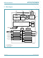
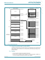
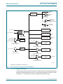
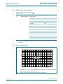
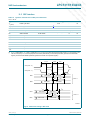
5. Block diagram
FT
FT
FT
FT
FT
LPC1311/13/42/43
NXP Semiconductors
D
FT
FT
A
A
R
R
D
D
D
XTALIN
XTALOUT
RESET
R
USB pins
SWD
A
FT
D
R
USB PHY(1)
TEST/DEBUG
INTERFACE
IRC
ARM
CORTEX-M3
I-code
bus
D-code
bus
A
LPC1311/13/42/43
USB DEVICE
CONTROLLER(1)
system
bus
CLOCK
GENERATION,
POWER CONTROL,
SYSTEM
FUNCTIONS
POR
CLKOUT
clocks and
controls
slave
slave
ROM
AHB-LITE BUS
GPIO ports
PIO0/1/2/3
slave
HIGH-SPEED
GPIO
RXD
TXD
DTR, DSR(2), CTS,
DCD(2), RI(2), RTS
CT32B0_MAT[3:0]
CT32B0_CAP0
CT32B1_MAT[3:0]
CT32B1_CAP0
CT16B0_MAT[2:0]
CT16B0_CAP0
CT16B1_MAT[1:0]
CT16B1_CAP0
slave
slave
slave
AHB TO
APB
BRIDGE
UART
SRAM
4/8 kB
FLASH
8/16/32 kB
10-bit ADC
AD[7:0]
SSP
SCK
SSEL
MISO
MOSI
32-bit COUNTER/TIMER 0
32-bit COUNTER/TIMER 1
16-bit COUNTER/TIMER 0
16-bit COUNTER/TIMER 1
SCL
SDA
I2C-BUS
WDT
IOCONFIG
SYSTEM CONTROL
002aae722
(1) LPC1342/43 only.
(2) LQFP48 package only.
Fig 1.
Block diagram
LPC1311_13_42_43_0
Preliminary data sheet
© NXP B.V. 2009. All rights reserved.
Rev. 00.14 — 20 August 2009
4 of 52
D
D
R
R
R
R
R
D
D
D
A
A
A
A
A
FT
D
R
R
A
A
FT
FT
FT
FT
A
A
R
R
D
D
D
D
R
R
A
FT
FT
FT
A
A
R
R
D
D
D
R
F
D
FT
FT
A
A
R
R
D
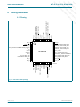
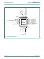
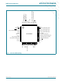
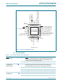
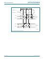
6.1 Pinning
A
FT
FT
A
A
R
R
D
D
D
6. Pinning information
FT
FT
FT
FT
LPC1311/13/42/43
NXP Semiconductors
D
D
R
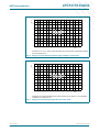
37 PIO3_1
38 PIO2_3/RI
39 SWDIO/PIO1_3/AD4/CT32B1_MAT2
40 PIO1_4/AD5/CT32B1_MAT3/WAKEUP
41 VSS
42 PIO1_11/AD7
43 PIO3_2
44 VDD(3V3)
A
45 PIO1_5/RTS/CT32B0_CAP0
R
46 PIO1_6/RXD/CT32B0_MAT0
D
47 PIO1_7/TXD/CT32B0_MAT1
FT
48 PIO3_3
A
PIO2_6
1
36 PIO3_0
PIO2_0/DTR
2
35 TRST/PIO1_2/AD3/CT32B1_MAT1
RESET/PIO0_0
3
34 TDO/PIO1_1/AD2/CT32B1_MAT0
PIO0_1/CLKOUT/CT32B0_MAT2/USB_FTOGGLE
4
33 TMS/PIO1_0/AD1/CT32B1_CAP0
VSSIO
5
32 TDI/PIO0_11/AD0/CT32B0_MAT3
XTALIN
6
XTALOUT
7
VDD(IO)
8
29 SWCLK/PIO0_10/SCK/CT16B0_MAT2
PIO1_8/CT16B1_CAP0
9
28 PIO0_9/MOSI/CT16B0_MAT1/SWO
31 PIO2_11/SCK
LPC1343FBD48
30 PIO1_10/AD6/CT16B1_MAT1
PIO0_2/SSEL/CT16B0_CAP0 10
27 PIO0_8/MISO/CT16B0_MAT0
Fig 2.
PIO2_9 24
PIO0_7/CTS 23
PIO0_6/USB_CONNECT/SCK 22
PIO2_5 21
USB_DP 20
USB_DM 19
PIO2_4 18
PIO1_9/CT16B1_MAT0 17
PIO0_5/SDA 16
PIO0_4/SCL 15
25 PIO2_10
PIO2_1/DSR 13
26 PIO2_2/DCD
PIO2_8 12
PIO0_3/USB_VBUS 14
PIO2_7 11
002aae505
LPC1343 LQFP48 package
LPC1311_13_42_43_0
Preliminary data sheet
© NXP B.V. 2009. All rights reserved.
Rev. 00.14 — 20 August 2009
5 of 52
D
D
R
R
R
R
R
D
D
D
D
R
R
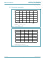
PIO1_11/AD7
PIO1_4/AD5/CT32B1_MAT3/WAKEUP
SWDIO/PIO1_3/AD4/CT32B1_MAT2
27
26
25
A
VDD(3V3)
R
PIO3_2
D
28
FT
PIO1_5/RTS/CT32B0_CAP0
A
29
R
PIO1_6/RXD/CT32B0_MAT0
TDI/PIO0_11/AD0/CT32B0_MAT3
XTALOUT
5
VDD(IO)
6
PIO1_8/CT16B1_CAP0
7
PIO0_2/SSEL/CT16B0_CAP0
8
14
15
16
USB_DP
PIO0_7/CTS
13
USB_DM
PIO0_6/USB_CONNECT/SCK
12
PIO1_9/CT16B1_MAT0
D
D
30
FT
FT
21
11
A
A
4
PIO0_5/SDA
R
R
TMS/PIO1_0/AD1/CT32B1_CAP0
XTALIN
20
PIO1_10/AD6/CT16B1_MAT1
19
SWCLK/PIO0_10/SCK/CT16B0_MAT2
18
PIO0_9/MOSI/CT16B0_MAT1/SWO
17
PIO0_8/MISO/CT16B0_MAT0
002aae516
Transparent top view
LPC1342/43 HVQFN33 package
Preliminary data sheet
© NXP B.V. 2009. All rights reserved.
Rev. 00.14 — 20 August 2009
F
D
D
22
LPC1311_13_42_43_0
A
FT
FT
PIO1_7/TXD/CT32B0_MAT1
R
A
A
31
D
R
R
3
PIO0_4/SCL
FT
D
D
32
A
FT
FT
TDO/PIO1_1/AD2/CT32B1_MAT0
PIO0_1/CLKOUT/CT32B0_MAT2/USB_FTOGGLE
9
R
R
A
A
TRST/PIO1_2/AD3/CT32B1_MAT1
23
10
D
D
R
R
24
2
33 VSS
FT
FT
D
D
1
PIO0_3/USB_VBUS
A
A
FT
FT
A
A
R
R
D
D
D
PIO2_0/DTR
RESET/PIO0_0
LPC1342FHN33
LPC1343FHN33
FT
FT
FT
FT
FT
terminal 1
index area
Fig 3.
A
A
A
A
A
LPC1311/13/42/43
NXP Semiconductors
6 of 52
R
R
R
R
R
D
R
R
FT
FT
D
D
R
A
FT
D
R
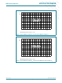
37 PIO3_1
38 PIO2_3/RI
A
39 SWDIO/PIO1_3/AD4/CT32B1_MAT2
A
A
40 PIO1_4/AD5/CT32B1_MAT3/WAKEUP
R
R
3
34 TDO/PIO1_1/AD2/CT32B1_MAT0
PIO0_1/CLKOUT/CT32B0_MAT2
4
33 TMS/PIO1_0/AD1/CT32B1_CAP0
VSSIO
5
32 TDI/PIO0_11/AD0/CT32B0_MAT3
XTALIN
6
XTALOUT
7
VDD(IO)
8
29 SWCLK/PIO0_10/SCK/CT16B0_MAT2
PIO1_8/CT16B1_CAP0
9
28 PIO0_9/MOSI/CT16B0_MAT1/SWO
31 PIO2_11/SCK
LPC1313FBD48
30 PIO1_10/AD6/CT16B1_MAT1
PIO0_2/SSEL/CT16B0_CAP0 10
27 PIO0_8/MISO/CT16B0_MAT0
PIO2_9 24
PIO0_7/CTS 23
PIO0_6/SCK 22
PIO3_5 21
PIO2_5 20
PIO2_4 19
PIO3_4 18
25 PIO2_10
PIO1_9/CT16B1_MAT0 17
26 PIO2_2/DCD
PIO2_8 12
PIO0_5/SDA 16
PIO2_7 11
PIO0_4/SCL 15
F
D
D
35 TRST/PIO1_2/AD3/CT32B1_MAT1
RESET/PIO0_0
PIO0_3 14
A
FT
FT
41 VSS
R
A
A
42 PIO1_11/AD7
D
R
R
43 PIO3_2
FT
D
D
44 VDD(3V3)
A
FT
FT
45 PIO1_5/RTS/CT32B0_CAP0
R
R
A
A
46 PIO1_6/RXD/CT32B0_MAT0
D
D
R
R
47 PIO1_7/TXD/CT32B0_MAT1
FT
FT
D
D
48 PIO3_3
A
A
FT
FT
A
A
R
R
D
D
D
36 PIO3_0
2
PIO2_1/DSR 13
FT
FT
FT
FT
FT
1
002aae513
LPC1313 LQFP48 package
LPC1311_13_42_43_0
Preliminary data sheet
A
A
A
A
A
PIO2_6
PIO2_0/DTR
Fig 4.
D
D
D
D
D
LPC1311/13/42/43
NXP Semiconductors
© NXP B.V. 2009. All rights reserved.
Rev. 00.14 — 20 August 2009
7 of 52
D
D
R
R
R
R
R
D
D
D
D
R
R
PIO1_11/AD7
PIO1_4/AD5/CT32B1_MAT3/WAKEUP
SWDIO/PIO1_3/AD4/CT32B1_MAT2
27
26
25
A
VDD(3V3)
R
PIO3_2
D
28
FT
PIO1_5/RTS/CT32B0_CAP0
A
29
R
PIO1_6/RXD/CT32B0_MAT0
TDI/PIO0_11/AD0/CT32B0_MAT3
XTALOUT
5
VDD(IO)
6
PIO1_8/CT16B1_CAP0
7
PIO0_2/SSEL/CT16B0_CAP0
8
14
15
16
PIO3_5
PIO0_7/CTS
13
PIO3_4
PIO0_6/SCK
12
PIO1_9/CT16B1_MAT0
D
D
30
FT
FT
21
11
A
A
4
PIO0_5/SDA
R
R
TMS/PIO1_0/AD1/CT32B1_CAP0
XTALIN
20
PIO1_10/AD6/CT16B1_MAT1
19
SWCLK/PIO0_10/SCK/CT16B0_MAT2
18
PIO0_9/MOSI/CT16B0_MAT1/SWO
17
PIO0_8/MISO/CT16B0_MAT0
002aae517
LPC1311/13 HVQFN33 package
6.2 Pin description
LPC1313/43 LQFP48 pin description table
Symbol
Pin
Type
Description
RESET/PIO0_0
3
I
RESET — External reset input: A LOW on this pin resets the device,
causing I/O ports and peripherals to take on their default states, and
processor execution to begin at address 0.
I/O
PIO0_0 — General purpose digital input/output pin.
PIO0_1/CLKOUT/
CT32B0_MAT2/
USB_FTOGGLE
4[1]
I/O
PIO0_1 — General purpose digital input/output pin. A LOW level on this pin
during reset starts the ISP command handler or the USB device
enumeration (USB on LPC1343 only, see description of PIO0_3).
O
CLKOUT — Clockout pin.
O
CT32B0_MAT2 — Match output 2 for 32-bit timer 0.
O
USB_FTOGGLE — USB 1 ms Start-of-Frame signal (LPC1343 only).
I/O
PIO0_2 — General purpose digital input/output pin.
O
SSEL — Slave select for SSP.
I
CT16B0_CAP0 — Capture input 0 for 16-bit timer 0.
PIO0_2/SSEL/
CT16B0_CAP0
10[1]
LPC1311_13_42_43_0
Preliminary data sheet
© NXP B.V. 2009. All rights reserved.
Rev. 00.14 — 20 August 2009
F
D
D
22
Transparent top view
Table 3.
A
FT
FT
PIO1_7/TXD/CT32B0_MAT1
R
A
A
31
D
R
R
32
FT
D
D
3
9
A
FT
FT
TDO/PIO1_1/AD2/CT32B1_MAT0
PIO0_1/CLKOUT/CT32B0_MAT2
10
R
R
A
A
TRST/PIO1_2/AD3/CT32B1_MAT1
23
PIO0_3
D
D
R
R
24
2
33 VSS
FT
FT
D
D
1
PIO0_4/SCL
A
A
FT
FT
A
A
R
R
D
D
D
PIO2_0/DTR
RESET/PIO0_0
LPC1311FHN33
LPC1313FHN33
FT
FT
FT
FT
FT
terminal 1
index area
Fig 5.
A
A
A
A
A
LPC1311/13/42/43
NXP Semiconductors
8 of 52
R
R
R
R
R
A
A
A
A
A
FT
D
R
R
A
A
FT
FT
FT
FT
A
A
R
R
D
D
D
D
R
R
A
FT
FT
FT
A
A
R
R
D
D
D
R
Type
Description
PIO0_3/USB_VBUS
14[1]
I/O
PIO0_3 — General purpose digital input/output pin. LPC1343 only: A LOW
level on this pin during reset starts the ISP command handler, a HIGH level
starts the USB device enumeration.
I
USB_VBUS — Monitors the presence of USB bus power (LPC1343 only).
A
A
Pin
PIO0_4/SCL
15[2]
I/O
PIO0_4 — General purpose digital input/output pin.
I/O
SCL — I2C-bus clock input/output. High-current sink only if I2C Fast-Mode
Plus is selected in the I/O configuration register.
I/O
PIO0_5 — General purpose digital input/output pin.
I/O
SDA — I2C-bus data input/output. High-current sink only if I2C Fast-Mode
Plus is selected in the I/O configuration register.
I/O
PIO0_6 — General purpose digital input/output pin.
O
USB_CONNECT — Signal used to switch an external 1.5 kΩ resistor under
software control. Used with the SoftConnect USB feature (LPC1343 only).
I/O
SCK — Serial clock for SSP.
I/O
PIO0_7 — General purpose digital input/output pin (high-current output
driver).
I
CTS — Clear To Send input for UART.
I/O
PIO0_8 — General purpose digital input/output pin.
I/O
MISO — Master In Slave Out for SSP.
O
CT16B0_MAT0 — Match output 0 for 16-bit timer 0.
I/O
PIO0_9 — General purpose digital input/output pin.
I/O
MOSI — Master Out Slave In for SSP.
O
CT16B0_MAT1 — Match output 1 for 16-bit timer 0.
O
SWO — Serial wire trace output.
I
SWCLK — Serial wire clock and test clock TCK for JTAG interface.
I/O
PIO0_10 — General purpose digital input/output pin.
O
SCK — Serial clock for SSP.
O
CT16B0_MAT2 — Match output 2 for 16-bit timer 0.
I
TDI — Test Data In for JTAG interface.
I/O
PIO0_11 — General purpose digital input/output pin.
I
AD0 — A/D converter, input 0.
O
CT32B0_MAT3 — Match output 3 for 32-bit timer 0.
I
TMS — Test Mode Select for JTAG interface.
I/O
PIO1_0 — General purpose digital input/output pin.
I
AD1 — A/D converter, input 1.
I
CT32B1_CAP0 — Capture input 0 for 32-bit timer 1.
O
TDO — Test Data Out for JTAG interface.
I/O
PIO1_1 — General purpose digital input/output pin.
I
AD2 — A/D converter, input 2.
O
CT32B1_MAT0 — Match output 0 for 32-bit timer 1.
F
FT
FT
Symbol
D
A
A
R
R
D
D
D
LPC1313/43 LQFP48 pin description table …continued
FT
FT
FT
FT
Table 3.
D
D
D
D
D
LPC1311/13/42/43
NXP Semiconductors
FT
FT
A
A
R
R
D
D
D
R
PIO0_8/MISO/
CT16B0_MAT0
27[1]
PIO0_9/MOSI/
CT16B0_MAT1/
SWO
SWCLK/PIO0_10/
SCK/CT16B0_MAT2
TDI/PIO0_11/
AD0/CT32B0_MAT3
TMS/PIO1_0/
AD1/CT32B1_CAP0
TDO/PIO1_1/
AD2/CT32B1_MAT0
28[1]
29[1]
32[3]
33[3]
34[3]
LPC1311_13_42_43_0
Preliminary data sheet
A
PIO0_7/CTS
23[1]
R
PIO0_6/USB_CONNECT/ 22[1]
SCK
D
16[2]
© NXP B.V. 2009. All rights reserved.
Rev. 00.14 — 20 August 2009
FT
PIO0_5/SDA
9 of 52
R
R
R
R
R
A
A
A
A
A
PIO1_7 — General purpose digital input/output pin.
O
TXD — Transmitter output for UART.
R
I/O
D
CT32B0_MAT0 — Match output 0 for 32-bit timer 0.
D
O
F
RXD — Receiver input for UART.
A
I
R
PIO1_6 — General purpose digital input/output pin.
D
CT32B0_CAP0 — Capture input 0 for 32-bit timer 0.
I/O
FT
I
FT
RTS — Request To Send output for UART.
FT
O
R
PIO1_5 — General purpose digital input/output pin.
A
I/O
A
WAKEUP — Deep power-down mode wake-up pin.
D
CT32B1_MAT3 — Match output 3 for 32-bit timer 1.
I
FT
O
R
AD5 — A/D converter, input 5.
R
I
D
PIO1_4 — General purpose digital input/output pin.
D
I/O
FT
CT32B1_MAT2 — Match output 2 for 32-bit timer 1.
A
AD4 — A/D converter, input 4.
O
FT
I
FT
PIO1_3 — General purpose digital input/output pin.
A
I/O
A
SWDIO — Serial wire debug input/output.
R
I/O
R
CT32B1_MAT1 — Match output 1 for 32-bit timer 1.
D
AD3 — A/D converter, input 3.
O
D
I
FT
PIO1_2 — General purpose digital input/output pin.
A
I/O
R
TRST — Test Reset for JTAG interface.
D
I
R
FT
FT
TRST/PIO1_2/
AD3/CT32B1_MAT1
D
A
A
Description
A
FT
R
R
Type
35[3]
R
A
D
D
Pin
D
R
FT
FT
A
A
R
R
D
D
D
LPC1313/43 LQFP48 pin description table …continued
Symbol
FT
FT
FT
FT
Table 3.
D
D
D
D
D
LPC1311/13/42/43
NXP Semiconductors
PIO1_4/AD5/
CT32B1_MAT3/WAKEUP
40[3]
PIO1_5/RTS/
CT32B0_CAP0
45[1]
PIO1_6/RXD/
CT32B0_MAT0
46[1]
PIO1_7/TXD/
CT32B0_MAT1
47[1]
O
CT32B0_MAT1 — Match output 1 for 32-bit timer 0.
PIO1_8/CT16B1_CAP0
9[1]
I/O
PIO1_8 — General purpose digital input/output pin.
I
CT16B1_CAP0 — Capture input 0 for 16-bit timer 1.
PIO1_9/CT16B1_MAT0
17[1]
I/O
PIO1_9 — General purpose digital input/output pin.
O
CT16B1_MAT0 — Match output 0 for 16-bit timer 1.
PIO1_10/AD6/
CT16B1_MAT1
30[3]
I/O
PIO1_10 — General purpose digital input/output pin.
I
AD6 — A/D converter, input 6.
O
CT16B1_MAT1 — Match output 1 for 16-bit timer 1.
I/O
PIO1_11 — General purpose digital input/output pin.
I
AD7 — A/D converter, input 7.
I/O
PIO2_0 — General purpose digital input/output pin.
O
DTR — Data Terminal Ready output for UART.
I/O
PIO2_1 — General purpose digital input/output pin.
I
DSR — Data Set Ready input for UART.
I/O
PIO2_2 — General purpose digital input/output pin.
I
DCD — Data Carrier Detect input for UART.
I/O
PIO2_3 — General purpose digital input/output pin.
PIO1_11/AD7
42[3]
PIO2_0/DTR
2[1]
PIO2_1/DSR
13[1]
PIO2_2/DCD
26[1]
A
SWDIO/PIO1_3/AD4/
CT32B1_MAT2
39[3]
PIO2_3/RI
38[1]
I
RI — Ring Indicator input for UART.
PIO2_4
18[1]
I/O
PIO2_4 — General purpose digital input/output pin (LPC1343 only).
PIO2_4
19[1]
I/O
PIO2_4 — General purpose digital input/output pin (LPC1313 only).
PIO2_5
21[1]
I/O
PIO2_5 — General purpose digital input/output pin (LPC1343 only).
LPC1311_13_42_43_0
Preliminary data sheet
© NXP B.V. 2009. All rights reserved.
Rev. 00.14 — 20 August 2009
10 of 52
R
R
R
R
R
A
A
A
A
A
D
R
R
A
A
FT
FT
FT
FT
A
A
R
R
D
D
D
D
R
R
A
FT
FT
FT
A
A
R
R
D
D
D
R
Pin
Type
Description
PIO2_5
20[1]
I/O
PIO2_5 — General purpose digital input/output pin (LPC1313 only).
PIO2_6
1[1]
I/O
PIO2_6 — General purpose digital input/output pin.
PIO2_7
11[1]
I/O
PIO2_7 — General purpose digital input/output pin.
PIO2_8
12[1]
I/O
PIO2_8 — General purpose digital input/output pin.
PIO2_9
24[1]
I/O
PIO2_9 — General purpose digital input/output pin.
PIO2_10
25[1]
I/O
PIO2_10 — General purpose digital input/output pin.
PIO2_11/SCK
31[1]
I/O
PIO2_11 — General purpose digital input/output pin.
I/O
SCK — Serial clock for SSP.
PIO3_0
36[1]
I/O
PIO3_0 — General purpose digital input/output pin.
PIO3_1
37[1]
I/O
PIO3_1 — General purpose digital input/output pin.
PIO3_2
43[1]
I/O
PIO3_2 — General purpose digital input/output pin.
PIO3_3
48[1]
I/O
PIO3_3 — General purpose digital input/output pin.
PIO3_4
18[1]
I/O
PIO3_4 — General purpose digital input/output pin (LPC1313 only).
PIO3_5
21[1]
I/O
PIO3_5 — General purpose digital input/output pin (LPC1313 only).
USB_DM
19[4]
I/O
USB_DM — USB bidirectional D− line (LPC1343 only).
USB_DP
20[4]
I/O
USB_DP — USB bidirectional D+ line (LPC1343 only).
VDD(IO)
8
I
3.3 V input/output supply voltage.
VDD(3V3)
44
I
3.3 V supply voltage to the internal regulator and the ADC. Also used as the
ADC reference voltage.
VSSIO
5
I
Ground.
XTALIN
6
I
Input to the oscillator circuit and internal clock generator circuits. Input
voltage must not exceed 1.8 V.
F
FT
FT
Symbol
A
A
A
R
R
D
D
D
LPC1313/43 LQFP48 pin description table …continued
FT
FT
FT
FT
FT
Table 3.
D
D
D
D
D
LPC1311/13/42/43
NXP Semiconductors
D
FT
FT
A
A
R
R
D
D
D
R
A
FT
D
R
7
O
Output from the oscillator amplifier.
VSS
41
I
Ground.
A
XTALOUT
[1]
5 V tolerant pad providing digital I/O functions with configurable pull-up/pull-down resistors and configurable hysteresis.
[2]
I2C-bus pads compliant with the I2C-bus specification for I2C standard mode and I2C Fast-mode Plus.
[3]
5 V tolerant pad providing digital I/O functions with configurable pull-up/pull-down resistors, configurable hysteresis, and analog input.
When configured as a ADC input, digital section of the pad is disabled and the pin is not 5 V tolerant.
[4]
Pad provides USB functions. It is designed in accordance with the USB specification, revision 2.0 (Full-speed and Low-speed mode
only).
Table 4.
LPC1311/13/42/43 HVQFN33 pin description table
Symbol
Pin
Type
Description
RESET/PIO0_0
2
I
RESET — External reset input: A LOW on this pin resets the device,
causing I/O ports and peripherals to take on their default states, and
processor execution to begin at address 0.
I/O
PIO0_0 — General purpose digital input/output pin.
PIO0_1/CLKOUT/
CT32B0_MAT2/
USB_FTOGGLE
3[1]
I/O
PIO0_1 — General purpose digital input/output pin. A LOW level on this pin
during reset starts the ISP command handler or the USB device
enumeration (USB on LPC1342/43 only, see description of PIO0_3).
O
CLKOUT — Clock out pin.
O
CT32B0_MAT2 — Match output 2 for 32-bit timer 0.
O
USB_FTOGGLE — USB 1 ms Start-of-Frame signal (LPC1342/43 only).
LPC1311_13_42_43_0
Preliminary data sheet
© NXP B.V. 2009. All rights reserved.
Rev. 00.14 — 20 August 2009
11 of 52
R
R
R
R
R
D
R
R
A
A
FT
FT
FT
FT
A
A
R
R
D
D
D
D
A
FT
R
PIO0_2/SSEL/
CT16B0_CAP0
I/O
PIO0_2 — General purpose digital input/output pin.
O
SSEL — Slave select for SSP.
I
CT16B0_CAP0 — Capture input 0 for 16-bit timer 0.
PIO0_3/USB_VBUS
9[1]
I/O
PIO0_3 — General purpose digital input/output pin. LPC1342/43 only: A
LOW level on this pin during reset starts the ISP command handler, a HIGH
level starts the USB device enumeration.
I
USB_VBUS — Monitors the presence of USB bus power (LPC1342/43
only).
I/O
PIO0_4 — General purpose digital input/output pin.
I/O
SCL — I2C-bus clock input/output. High-current sink only if I2C Fast-Mode
Plus is selected in the I/O configuration register.
I/O
PIO0_5 — General purpose digital input/output pin.
I/O
SDA — I2C-bus data input/output. High-current sink only if I2C Fast-Mode
Plus is selected in the I/O configuration register.
I/O
PIO0_6 — General purpose digital input/output pin.
O
USB_CONNECT — Signal used to switch an external 1.5 kΩ resistor under
software control. Used with the SoftConnect USB feature (LPC1342/43
only).
CT16B0_MAT0 — Match output 0 for 16-bit timer 0.
I/O
PIO0_9 — General purpose digital input/output pin.
I/O
MOSI — Master Out Slave In for SSP.
O
CT16B0_MAT1 — Match output 1 for 16-bit timer 0.
O
SWO — Serial wire trace output.
I
SWCLK — Serial wire clock and test clock TCK for JTAG interface.
O
CT16B0_MAT2 — Match output 2 for 16-bit timer 0.
I
TDI — Test Data In for JTAG interface.
I/O
PIO0_11 — General purpose digital input/output pin.
I
AD0 — A/D converter, input 0.
O
CT32B0_MAT3 — Match output 3 for 32-bit timer 0.
I
TMS — Test Mode Select for JTAG interface.
I/O
PIO1_0 — General purpose digital input/output pin.
I
AD1 — A/D converter, input 1.
I
CT32B1_CAP0 — Capture input 0 for 32-bit timer 1.
© NXP B.V. 2009. All rights reserved.
Rev. 00.14 — 20 August 2009
12 of 52
A
O
R
MISO — Master In Slave Out for SSP.
D
PIO0_8 — General purpose digital input/output pin.
I/O
PIO0_10 — General purpose digital input/output pin.
D
I/O
SCK — Serial clock for SSP.
F
CTS — Clear To Send input for UART.
FT
I
I/O
FT
SCK — Serial clock for SSP.
PIO0_7 — General purpose digital input/output pin (high-current output
driver).
LPC1311_13_42_43_0
Preliminary data sheet
A
I/O
I/O
O
A
TMS/PIO1_0/AD1/
CT32B1_CAP0
22[3]
R
TDI/PIO0_11/AD0/
CT32B0_MAT3
21[3]
R
SWCLK/PIO0_10/SCK/
CT16B0_MAT2
19[1]
D
PIO0_9/MOSI/
CT16B0_MAT1/
SWO
18[1]
D
PIO0_8/MISO/
CT16B0_MAT0
17[1]
FT
16[1]
A
PIO0_7/CTS
R
15[1]
D
PIO0_6/USB_CONNECT/
SCK
FT
11[2]
FT
Description
A
A
A
R
R
D
D
D
Type
8[1]
PIO0_5/SDA
R
R
FT
FT
A
A
R
R
D
D
D
Pin
10[2]
FT
FT
FT
FT
FT
LPC1311/13/42/43 HVQFN33 pin description table …continued
Symbol
PIO0_4/SCL
A
A
A
A
A
Table 4.
D
D
D
D
D
LPC1311/13/42/43
NXP Semiconductors
R
R
R
R
R
A
A
A
A
A
CT32B0_CAP0 — Capture input 0 for 32-bit timer 0.
I/O
PIO1_6 — General purpose digital input/output pin.
I
RXD — Receiver input for UART.
O
CT32B0_MAT0 — Match output 0 for 32-bit timer 0.
I/O
PIO1_7 — General purpose digital input/output pin.
O
TXD — Transmitter output for UART.
R
I
D
RTS — Request To Send output for UART.
D
O
F
PIO1_5 — General purpose digital input/output pin.
A
I/O
R
WAKEUP — Deep power-down mode wake-up pin.
D
CT32B1_MAT3 — Match output 3 for 32-bit timer 1.
I
FT
O
FT
AD5 — A/D converter, input 5.
FT
I
R
PIO1_4 — General purpose digital input/output pin.
A
I/O
A
CT32B1_MAT2 — Match output 2 for 32-bit timer 1.
D
AD4 — A/D converter, input 4.
O
FT
I
R
PIO1_3 — General purpose digital input/output pin.
R
I/O
D
SWDIO — Serial wire debug input/output.
D
I/O
FT
CT32B1_MAT1 — Match output 1 for 32-bit timer 1.
A
AD3 — A/D converter, input 3.
O
FT
I
FT
PIO1_2 — General purpose digital input/output pin.
A
I/O
A
TRST — Test Reset for JTAG interface.
R
I
R
CT32B1_MAT0 — Match output 0 for 32-bit timer 1.
D
AD2 — A/D converter, input 2.
O
D
I
FT
PIO1_1 — General purpose digital input/output pin.
A
I/O
R
TDO — Test Data Out for JTAG interface.
D
O
R
FT
FT
TDO/PIO1_1/AD2/
CT32B1_MAT0
D
A
A
Description
A
FT
R
R
Type
23[3]
R
A
D
D
Pin
D
R
FT
FT
A
A
R
R
D
D
D
LPC1311/13/42/43 HVQFN33 pin description table …continued
Symbol
FT
FT
FT
FT
Table 4.
D
D
D
D
D
LPC1311/13/42/43
NXP Semiconductors
SWDIO/PIO1_3/AD4/
CT32B1_MAT2
PIO1_4/AD5/
CT32B1_MAT3/WAKEUP
25[3]
26[3]
A
TRST/PIO1_2/AD3/
CT32B1_MAT1
24[3]
PIO1_5/RTS/
CT32B0_CAP0
30[1]
PIO1_6/RXD/
CT32B0_MAT0
31[1]
PIO1_7/TXD/
CT32B0_MAT1
32[1]
O
CT32B0_MAT1 — Match output 1 for 32-bit timer 0.
PIO1_8/CT16B1_CAP0
7[1]
I/O
PIO1_8 — General purpose digital input/output pin.
I
CT16B1_CAP0 — Capture input 0 for 16-bit timer 1.
PIO1_9/CT16B1_MAT0
12[1]
I/O
PIO1_9 — General purpose digital input/output pin.
O
CT16B1_MAT0 — Match output 0 for 16-bit timer 1.
PIO1_10/AD6/
CT16B1_MAT1
20[3]
I/O
PIO1_10 — General purpose digital input/output pin.
I
AD6 — A/D converter, input 6.
O
CT16B1_MAT1 — Match output 1 for 16-bit timer 1.
I/O
PIO1_11 — General purpose digital input/output pin.
I
AD7 — A/D converter, input 7.
I/O
PIO2_0 — General purpose digital input/output pin.
O
DTR — Data Terminal Ready output for UART.
PIO3_2
28[1]
I/O
PIO3_2 — General purpose digital input/output pin.
PIO3_4
13[1]
I/O
PIO3_4 — General purpose digital input/output pin (LPC1311/13 only).
PIO3_5
14[1]
I/O
PIO3_5 — General purpose digital input/output pin (LPC1311/13 only).
USB_DM
13[4]
I/O
USB_DM — USB bidirectional D− line (LPC1342/43 only).
USB_DP
14[4]
I/O
USB_DP — USB bidirectional D+ line (LPC1342/43 only).
PIO1_11/AD7
27[3]
PIO2_0/DTR
1[1]
LPC1311_13_42_43_0
Preliminary data sheet
© NXP B.V. 2009. All rights reserved.
Rev. 00.14 — 20 August 2009
13 of 52
R
R
R
R
R
FT
FT
FT
FT
FT
D
R
R
A
A
FT
FT
FT
FT
A
A
R
R
D
D
D
D
R
R
A
FT
FT
FT
A
A
R
R
D
D
D
R
Type
Description
VDD(IO)
6
I
3.3 V input/output supply voltage.
VDD(3V3)
29
I
3.3 V supply voltage to the internal DC-DC converter and the ADC. Also
used as the ADC reference voltage.
XTALIN
4
I
Input to the oscillator circuit and internal clock generator circuits. Input
voltage must not exceed 1.8 V.
XTALOUT
5
O
Output from the oscillator amplifier.
VSS
33
-
Thermal pad. Connect to ground.
F
FT
FT
Pin
A
A
A
R
R
D
D
D
LPC1311/13/42/43 HVQFN33 pin description table …continued
Symbol
D
FT
FT
A
A
R
R
D
D
D
R
[4]
Pad provides USB functions. It is designed in accordance with the USB specification, revision 2.0 (Full-speed and Low-speed mode
only).
7. Functional description
7.1 Architectural overview
The ARM Cortex-M3 includes three AHB-Lite buses: the system bus, the I-code bus, and
the D-code bus (see Figure 1). The I-code and D-code core buses are faster than the
system bus and are used similarly to TCM interfaces: one bus dedicated for instruction
fetch (I-code) and one bus for data access (D-code). The use of two core buses allows for
simultaneous operations if concurrent operations target different devices.
7.2 ARM Cortex-M3 processor
The ARM Cortex-M3 is a general purpose, 32-bit microprocessor, which offers high
performance and very low power consumption. The ARM Cortex-M3 offers many new
features, including a Thumb-2 instruction set, low interrupt latency, hardware divide,
interruptable/continuable multiple load and store instructions, automatic state save and
restore for interrupts, tightly integrated interrupt controller, and multiple core buses
capable of simultaneous accesses.
Pipeline techniques are employed so that all parts of the processing and memory systems
can operate continuously. Typically, while one instruction is being executed, its successor
is being decoded, and a third instruction is being fetched from memory.
The ARM Cortex-M3 processor is described in detail in the Cortex-M3 Technical
Reference Manual which is available on the official ARM website.
7.3 On-chip flash program memory
The LPC1311/13/42/43 contain 32 kB (LPC1313 and LPC1343), 16 kB (LPC1342), or
8 kB (LPC1311) of on-chip flash memory.
7.4 On-chip SRAM
The LPC1311/13/42/43 contain a total of 8 kB (LPC1343 and LPC1313) or 4 kB (LPC1342
and LPC1311) on-chip static RAM memory.
LPC1311_13_42_43_0
© NXP B.V. 2009. All rights reserved.
Rev. 00.14 — 20 August 2009
14 of 52
A
5 V tolerant pad providing digital I/O functions with configurable pull-up/pull-down resistors, configurable hysteresis, and analog input.
When configured as a ADC input, digital section of the pad is disabled, and the pin is not 5 V tolerant.
R
[3]
D
I2C-bus pads compliant with the I2C-bus specification for I2C standard mode and I2C Fast-mode Plus.
FT
5 V tolerant pad providing digital I/O functions with configurable pull-up/pull-down resistors and configurable hysteresis.
[2]
A
[1]
Preliminary data sheet
A
A
A
A
A
Table 4.
D
D
D
D
D
LPC1311/13/42/43
NXP Semiconductors
D
D
R
R
R
R
R
D
D
D
A
A
A
A
A
FT
D
R
R
A
A
FT
FT
FT
FT
A
A
R
R
D
D
D
D
R
R
A
FT
FT
FT
A
A
R
R
D
D
D
R
A
FT
FT
A
A
R
R
D
D
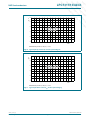
The LPC134x incorporates several distinct memory regions, shown in the following
figures. Figure 6 shows the overall map of the entire address space from the user
program viewpoint following reset. The interrupt vector area supports address remapping.
F
FT
FT
A
A
R
R
D
D
D
7.5 Memory map
FT
FT
FT
FT
LPC1311/13/42/43
NXP Semiconductors
D
D
R
A
15 of 52
A
© NXP B.V. 2009. All rights reserved.
Rev. 00.14 — 20 August 2009
R
Preliminary data sheet
D
LPC1311_13_42_43_0
FT
The AHB peripheral area is 2 MB in size and is divided to allow for up to 128 peripherals.
The APB peripheral area is 1 MB in size and is divided to allow for up to 64 peripherals.
Each peripheral of either type is allocated 16 kB of space. This allows simplifying the
address decoding for each peripheral.
R
R
R
R
R
A
A
A
A
A
D
R
R
A
A
FT
FT
FT
FT
A
A
R
R
D
D
D
D
A
FT
R
A
F
FT
FT
A
A
R
R
D
D
D
0x5020 0000
D
FT
FT
A
A
R
R
D
0xFFFF FFFF
R
R
FT
FT
A
A
R
R
D
D
D
AHB peripherals
LPC1311/13/42/43
FT
FT
FT
FT
FT
4 GB
D
D
D
D
D
LPC1311/13/42/43
NXP Semiconductors
D
D
127- 4 reserved
R
A
reserved
1
GPIO PIO1
0
GPIO PIO0
0x5003 0000
0x5002 0000
0x5001 0000
0x5000 0000
reserved
APB peripherals
0x4008 0000
1 GB
APB peripherals
0x4008 0000
31 - 19 reserved
0x4000 0000
0x4004 C000
reserved
0x2400 0000
AHB SRAM bit-band alias addressing
0x2200 0000
reserved
18
system control
17
IOCONFIG
16
15
SSP
reserved
14
PMU
0x4004 8000
0x4004 4000
0x4004 0000
0x4003 C000
0x4003 8000
0x2000 0000
0.5 GB
10 - 13 reserved
reserved
0x4002 8000
0x1FFF 4000
16 kB boot ROM
0x1FFF 0000
reserved
0x1000 2000
8 kB SRAM (LPC1313/1343)
I-code/D-code
memory space
4 kB SRAM (LPC1311/1342)
0x1000 1000
0x1000 0000
reserved
9
reserved
8
USB (LPC1342/43 only)
0x4002 0000
7
ADC
0x4001 C000
6
32-bit counter/timer 1
0x4001 8000
5
32-bit counter/timer 0
0x4001 4000
4
16-bit counter/timer 1
0x4001 0000
3
16-bit counter/timer 0
0x4000 C000
2
UART
0x4000 8000
1
0
WDT
0x4000 4000
I2C-bus
0x4000 0000
0x4002 4000
0x0000 8000
32 kB on-chip flash (LPC1313/43)
16 kB on-chip flash (LPC1342)
0 GB
8 kB on-chip flash (LPC1311)
0x0000 4000
0x0000 2000
+ 512 byte
active interrupt vectors
0x0000 0200
0x0000 0000
0x0000 0000
002aae723
Fig 6.
LPC1311/13/42/43 memory map
7.6 Nested Vectored Interrupt Controller (NVIC)
The Nested Vectored Interrupt Controller (NVIC) is an integral part of the Cortex-M3. The
tight coupling to the CPU allows for low interrupt latency and efficient processing of late
arriving interrupts.
7.6.1 Features
• Controls system exceptions and peripheral interrupts.
• On the LPC1311/13/42/43, the NVIC supports 16 vectored interrupts. In addition, up
to 40 of the individual GPIO inputs are NVIC-vector capable.
LPC1311_13_42_43_0
Preliminary data sheet
© NXP B.V. 2009. All rights reserved.
Rev. 00.14 — 20 August 2009
16 of 52
A
0x5000 0000
GPIO PIO2
R
AHB peripherals
2
D
0x5020 0000
GPIO PIO3
FT
0x5004 0000
3
D
D
R
R
R
R
R
D
D
D
FT
FT
FT
FT
FT
D
R
R
A
A
FT
FT
FT
FT
A
A
R
R
D
D
D
D
R
R
A
FT
FT
FT
A
A
R
R
D
D
D
R
A
F
FT
FT
A
A
R
R
D
D
D
• 8 programmable interrupt priority levels, with hardware priority level masking
• Relocatable vector table.
• Software interrupt generation.
D
FT
FT
A
A
R
R
D
D
D
R
7.6.2 Interrupt sources
A
Peripherals should be connected to the appropriate pins prior to being activated and prior
to any related interrupt(s) being enabled. Activity of any enabled peripheral function that is
not mapped to a related pin should be considered undefined.
7.8 Fast general purpose parallel I/O
Device pins that are not connected to a specific peripheral function are controlled by the
GPIO registers. Pins may be dynamically configured as inputs or outputs. Separate
registers allow setting or clearing any number of outputs simultaneously. The value of the
output register may be read back as well as the current state of the port pins.
LPC1311/13/42/43 use accelerated GPIO functions:
• GPIO registers are a dedicated AHB peripheral and are accessed through the AHB so
that the fastest possible I/O timing can be achieved.
• Entire port value can be written in one instruction.
Additionally, any GPIO pin (total of up to 42 pins) providing a digital function can be
programmed to generate an interrupt on a level, a rising or falling edge, or both.
7.8.1 Features
• Bit-level set and clear registers allow a single instruction to set or clear any number of
bits in one port.
• Direction control of individual bits.
• All I/O default to inputs with pull-up resistors enabled after reset.
• Pull-up/pull-down resistor configuration can be programmed through the IOCONFIG
block for each GPIO pin.
LPC1311_13_42_43_0
© NXP B.V. 2009. All rights reserved.
Rev. 00.14 — 20 August 2009
17 of 52
A
The IOCONFIG block allows selected pins of the microcontroller to have more than one
function. Configuration registers control the multiplexers to allow connection between the
pin and the on-chip peripherals.
R
7.7 IOCONFIG block
D
Any GPIO pin (total of up to 42 pins) regardless of the selected function, can be
programmed to generate an interrupt on a level, or rising edge or falling edge, or both.
FT
Each peripheral device has one interrupt line connected to the NVIC but may have several
interrupt flags. Individual interrupt flags may also represent more than one interrupt
source.
Preliminary data sheet
A
A
A
A
A
LPC1311/13/42/43
NXP Semiconductors
D
D
R
R
R
R
R
D
D
D
A
A
A
A
A
D
R
R
A
A
FT
FT
FT
FT
A
A
R
R
D
D
D
D
R
R
A
FT
FT
FT
A
A
R
R
D
D
D
R
A
FT
FT
A
A
R
R
D
D
The Universal Serial Bus (USB) is a 4-wire bus that supports communication between a
host and one or more (up to 127) peripherals. The host controller allocates the USB
bandwidth to attached devices through a token-based protocol. The bus supports
hot-plugging and dynamic configuration of the devices. All transactions are initiated by the
host controller.
F
FT
FT
A
A
R
R
D
D
D
7.9 USB interface (LPC1342/43 only)
FT
FT
FT
FT
FT
LPC1311/13/42/43
NXP Semiconductors
D
D
R
A
FT
D
R
A
The LPC1342/43 USB interface is a device controller with on-chip PHY for device
functions.
7.9.1 Full-speed USB device controller
The device controller enables 12 Mbit/s data exchange with a USB Host controller. It
consists of a register interface, serial interface engine, and endpoint buffer memory. The
serial interface engine decodes the USB data stream and writes data to the appropriate
endpoint buffer. The status of a completed USB transfer or error condition is indicated via
status registers. An interrupt is also generated if enabled.
7.9.1.1
Features
• Fully compliant with USB 2.0 specification (full speed).
• Supports 10 physical (5 logical) endpoints with up to 64 bytes buffer RAM per
endpoint (see Table 5).
• Supports Control, Bulk, Isochronous, and Interrupt endpoints.
• Supports SoftConnect feature.
• Double buffer implementation for Bulk and Isochronous endpoints.
Table 5.
USB device endpoint configuration
Logical
endpoint
Physical
endpoint
Endpoint type
Direction
Packet size
(byte)
Double buffer
0
0
Control
out
64
no
0
1
Control
in
64
no
1
2
Interrupt/Bulk
out
64
no
1
3
Interrupt/Bulk
in
64
no
2
4
Interrupt/Bulk
out
64
no
2
5
Interrupt/Bulk
in
64
no
3
6
Interrupt/Bulk
out
64
yes
3
7
Interrupt/Bulk
in
64
yes
4
8
Isochronous
out
512
yes
4
9
Isochronous
in
512
yes
7.10 UART
The LPC1311/13/42/43 contains one UART.
Support for RS-485/9-bit mode allows both software address detection and automatic
address detection using 9-bit mode.
The UART includes a fractional baud rate generator. Standard baud rates such as
115200 Bd can be achieved with any crystal frequency above 2 MHz.
LPC1311_13_42_43_0
Preliminary data sheet
© NXP B.V. 2009. All rights reserved.
Rev. 00.14 — 20 August 2009
18 of 52
D
D
R
R
R
R
D
R
R
A
A
FT
FT
FT
FT
A
A
R
R
D
D
D
D
R
R
A
FT
FT
FT
A
A
R
R
D
D
D
R
R
FT
FT
A
A
R
D
D
R
A
7.11.1 Features
• Compatible with Motorola SPI, 4-wire Texas Instruments SSI, and National
Semiconductor Microwire buses
Synchronous serial communication
Master or slave operation
8-frame FIFOs for both transmit and receive
4-bit to 16-bit frame
7.12 I2C-bus serial I/O controller
The LPC1311/13/42/43 contain one I2C-bus controller.
The I2C-bus is bidirectional for inter-IC control using only two wires: a serial clock line
(SCL) and a serial data line (SDA). Each device is recognized by a unique address and
can operate as either a receiver-only device (e.g., an LCD driver) or a transmitter with the
capability to both receive and send information (such as memory). Transmitters and/or
receivers can operate in either master or slave mode, depending on whether the chip has
to initiate a data transfer or is only addressed. The I2C is a multi-master bus and can be
controlled by more than one bus master connected to it.
7.12.1 Features
• The I2C-bus interface is a standard I2C-bus compliant interface with open-drain pins.
The I2C-bus interface also supports Fast-Mode Plus with bit rates up to 1 Mbit/s.
• Easy to configure as master, slave, or master/slave.
• Programmable clocks allow versatile rate control.
• Bidirectional data transfer between masters and slaves.
© NXP B.V. 2009. All rights reserved.
19 of 52
A
The LPC1311/13/42/43 contain one SSP controller. The SSP controller is capable of
operation on a SSP, 4-wire SSI, or Microwire bus. It can interact with multiple masters and
slaves on the bus. Only a single master and a single slave can communicate on the bus
during a given data transfer. The SSP supports full duplex transfers, with frames of 4 bits
to 16 bits of data flowing from the master to the slave and from the slave to the master. In
practice, often only one of these data flows carries meaningful data.
R
7.11 SSP serial I/O controller
D
• Support for RS-485/9-bit mode.
• Support for modem control.
FT
Built-in fractional baud rate generator covering wide range of baud rates without a
need for external crystals of particular values.
Rev. 00.14 — 20 August 2009
F
D
D
Receiver FIFO trigger points at 1 B, 4 B, 8 B, and 14 B.
mechanism that enables software flow control implementation.
Preliminary data sheet
A
FT
FT
A
A
R
R
D
D
D
Register locations conform to 16C550 industry standard.
LPC1311_13_42_43_0
FT
FT
FT
FT
FT
16-byte receive and transmit FIFOs.
• Fractional divider for baud rate control, auto baud capabilities and FIFO control
•
•
•
•
A
A
A
A
A
7.10.1 Features
•
•
•
•
R
D
D
D
LPC1311/13/42/43
NXP Semiconductors
D
D
R
R
R
R
R
D
D
D
A
A
A
A
A
D
R
R
A
A
FT
FT
FT
FT
A
A
R
R
D
D
D
D
R
R
A
FT
FT
FT
A
A
R
R
D
D
D
D
R
A
F
FT
FT
A
A
R
R
D
D
• Multi-master bus (no central master).
• Arbitration between simultaneously transmitting masters without corruption of serial
D
FT
FT
A
A
R
R
D
data on the bus.
FT
FT
FT
FT
FT
LPC1311/13/42/43
NXP Semiconductors
D
D
• Serial clock synchronization allows devices with different bit rates to communicate via
R
A
one serial bus.
A
7.13 10-bit ADC
The LPC1311/13/42/43 contains one ADC. It is a single 10-bit successive approximation
ADC with eight channels.
7.13.1 Features
10-bit successive approximation ADC.
Input multiplexing among 8 pins.
Power-down mode.
Measurement range 0 V to VDD(3V3).
10-bit conversion time ≥ 2.44 μs.
Burst conversion mode for single or multiple inputs.
Optional conversion on transition of input pin or Timer Match signal.
Individual result registers for each ADC channel to reduce interrupt overhead.
7.14 General purpose external event counters/timers
The LPC1311/13/42/43 includes two 32-bit counter/timers and two 16-bit counter/timers.
The counter/timer is designed to count cycles of the system derived clock. It can optionally
generate interrupts or perform other actions at specified timer values, based on four
match registers. Each counter/timer also includes one capture input to trap the timer value
when an input signal transitions, optionally generating an interrupt.
7.14.1 Features
• A 32-bit/16-bit timer/counter with a programmable 32-bit/16-bit prescaler.
• Counter or timer operation.
• One capture channel per timer, that can take a snapshot of the timer value when an
input signal transitions. A capture event may also generate an interrupt.
• Four match registers per timer that allow:
– Continuous operation with optional interrupt generation on match.
– Stop timer on match with optional interrupt generation.
– Reset timer on match with optional interrupt generation.
• Up to four external outputs corresponding to match registers, with the following
capabilities:
LPC1311_13_42_43_0
Preliminary data sheet
© NXP B.V. 2009. All rights reserved.
Rev. 00.14 — 20 August 2009
R
• The I2C-bus can be used for test and diagnostic purposes.
• The I2C-bus controller supports multiple address recognition and a bus monitor mode.
•
•
•
•
•
•
•
•
D
resume serial transfer.
FT
• Serial clock synchronization can be used as a handshake mechanism to suspend and
20 of 52
D
D
R
R
R
R
R
D
D
D
A
A
A
A
A
D
R
R
A
A
D
R
R
A
FT
FT
FT
A
A
R
R
D
D
D
R
F
D
FT
FT
A
A
R
R
D
– Toggle on match.
A
FT
FT
A
A
R
R
D
D
D
– Set HIGH on match.
FT
FT
FT
FT
A
A
R
R
D
D
D
– Set LOW on match.
FT
FT
FT
FT
FT
LPC1311/13/42/43
NXP Semiconductors
D
D
– Do nothing on match.
R
A
FT
D
7.15 System tick timer
R
A
The ARM Cortex-M3 includes a system tick timer (SYSTICK) that is intended to generate
a dedicated SYSTICK exception, normally set to a 10 ms interval.
7.16 Watchdog timer
The purpose of the watchdog is to reset the microcontroller within a reasonable amount of
time if it enters an erroneous state. When enabled, the watchdog will generate a system
reset if the user program fails to ‘feed’ (or reload) the watchdog within a predetermined
amount of time.
7.16.1 Features
• Internally resets chip if not periodically reloaded.
• Debug mode.
• Enabled by software but requires a hardware reset or a watchdog reset/interrupt to be
disabled.
•
•
•
•
Incorrect/incomplete feed sequence causes reset/interrupt if enabled.
Flag to indicate watchdog reset.
Programmable 32-bit timer with internal prescaler.
Selectable time period from (Tcy(WDCLK) × 256 × 4) to (Tcy(WDCLK) × 232 × 4) in
multiples of Tcy(WDCLK) × 4.
• The Watchdog Clock (WDCLK) source can be selected from the Internal RC oscillator
(IRC), the watchdog oscillator, or the main clock. This gives a wide range of potential
timing choices of watchdog operation under different power reduction conditions. It
also provides the ability to run the WDT from an entirely internal source that is not
dependent on an external crystal and its associated components and wiring for
increased reliability.
7.17 Clocking and power control
7.17.1 Crystal oscillators
The LPC1311/13/42/43 include three independent oscillators. These are the system
oscillator, the Internal RC oscillator (IRC), and the watchdog oscillator. Each oscillator can
be used for more than one purpose as required in a particular application.
Following reset, the LPC1311/13/42/43 will operate from the internal RC oscillator until
switched by software. This allows systems to operate without any external crystal and the
bootloader code to operate at a known frequency.
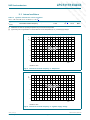
See Figure 7 for an overview of the LPC1311/13/42/43 clock generation.
LPC1311_13_42_43_0
Preliminary data sheet
© NXP B.V. 2009. All rights reserved.
Rev. 00.14 — 20 August 2009
21 of 52
D
D
R
R
R
R
R
D
D
D
A
A
A
A
A
D
R
R
A
A
D
R
R
A
FT
FT
FT
A
A
R
R
D
D
D
R
F
D
FT
FT
A
A
R
R
D
D
D
AHB clock 1
(ROM)
A
FT
FT
A
A
R
R
D
D
D
AHB clock 0
(system)
system clock
FT
FT
FT
FT
A
A
R
R
D
D
D
SYSTEM CLOCK
DIVIDER
FT
FT
FT
FT
FT
LPC1311/13/42/43
NXP Semiconductors
R
A
AHBCLKCTRL
(AHB clock enable)
FT
D
AHB clock 16
(IOCONFIG)
AHBCLKCTRL
IRC oscillator
SSP PERIPHERAL
CLOCK DIVIDER
main clock
watchdog oscillator
UART PERIPHERAL
CLOCK DIVIDER
MAINCLKSEL
(main clock select)
SYSTICK TIMER
CLOCK DIVIDER
IRC oscillator
system oscillator
SSP
UART
SYSTICK
timer
SYSTEM PLL
IRC oscillator
watchdog oscilllator
SYSPLLCLKSEL
(system PLL clock select)
WDT CLOCK
DIVIDER
WDT
USB 48 MHz CLOCK
DIVIDER
USB
CLKOUT PIN CLOCK
DIVIDER
CLKOUT pin
watchdog oscillator
WDTUEN
(WDT clock update enable)
USB PLL
system oscillator
USBPLLCLKSEL
(USB clock select)
USBUEN
(USB clock update enable)
IRC oscillator
system oscillator
watchdog oscillator
CLKOUTUEN
(CLKOUT update enable)
002aae859
The USB clock is available on LPC1342/43 only.
Fig 7.
LPC1311/13/42/43 clocking generation block diagram
7.17.1.1
Internal RC oscillator
The IRC may be used as the clock source for the WDT, and/or as the clock that drives the
system PLL and subsequently the CPU. The nominal IRC frequency is 12 MHz. The IRC
is trimmed to 1 % accuracy over the entire voltage and temperature range.
LPC1311_13_42_43_0
Preliminary data sheet
© NXP B.V. 2009. All rights reserved.
Rev. 00.14 — 20 August 2009
22 of 52
A
AHBCLKCTRL
R
AHB clocks
2 to 15
(memories
and peripherals)
14
D
D
R
R
R
R
R
D
D
D
A
A
A
A
A
FT
FT
FT
FT
FT
LPC1311/13/42/43
D
R
R
A
A
FT
FT
FT
FT
A
A
R
R
D
D
D
NXP Semiconductors
D
R
R
A
FT
FT
FT
A
A
R
R
D
D
D
D
R
A
F
FT
FT
A
A
R
R
D
D
Upon power-up, any chip reset, or wake-up from Deep power-down mode, the
LPC1311/13/42/43 use the IRC as the clock source. Software may later switch to one of
the other available clock sources.
D
FT
FT
A
A
R
R
D
D
System oscillator
D
7.17.1.2
R
A
The PLL accepts an input clock frequency in the range of 10 MHz to 25 MHz. The input
frequency is multiplied up to a high frequency with a Current Controlled Oscillator (CCO).
The multiplier can be an integer value from 1 to 32. The CCO operates in the range of
156 MHz to 320 MHz, so there is an additional divider in the loop to keep the CCO within
its frequency range while the PLL is providing the desired output frequency. The output
divider may be set to divide by 2, 4, 8, or 16 to produce the output clock. Since the
minimum output divider value is 2, it is insured that the PLL output has a 50 % duty cycle.
The PLL is turned off and bypassed following a chip reset and may be enabled by
software. The program must configure and activate the PLL, wait for the PLL to lock, and
then connect to the PLL as a clock source. The PLL settling time is 100 μs.
7.17.3 Clock output
The LPC1311/13/42/43 features a clock output function that routes the IRC oscillator, the
system oscillator, the watchdog oscillator, or the main clock to an output pin.
7.17.4 Wake-up process
The LPC1311/13/42/43 begin operation at power-up and when awakened from Deep
power-down mode by using the 12 MHz IRC oscillator as the clock source. This allows
chip operation to resume quickly. If the main oscillator or the PLL is needed by the
application, software will need to enable these features and wait for them to stabilize
before they are used as a clock source.
7.17.5 Power control
The LPC1311/13/42/43 support a variety of power control features. There are three
special modes of processor power reduction: Sleep mode, Deep-sleep mode, and Deep
power-down mode. The CPU clock rate may also be controlled as needed by changing
clock sources, reconfiguring PLL values, and/or altering the CPU clock divider value. This
allows a trade-off of power versus processing speed based on application requirements.
In addition, a register is provided for shutting down the clocks to individual on-chip
LPC1311_13_42_43_0
Preliminary data sheet
© NXP B.V. 2009. All rights reserved.
Rev. 00.14 — 20 August 2009
23 of 52
A
The LPC134x contain a system PLL and a dedicated PLL for generating the 48 MHz USB
clock. The LPC131x contain the system PLL only. The system and USB PLLs are
identical.
R
7.17.2 System PLL and USB PLL
D
The system oscillator operates at frequencies of 1 MHz to 25 MHz. This frequency can be
boosted to a higher frequency, up to the maximum CPU operating frequency, by the
system PLL. The ARM processor clock frequency is referred to as CCLK elsewhere in this
document.
FT
The system oscillator can be used as the clock source for the CPU, with or without using
the PLL. On the LPC134x, the system oscillator must be used to provide the clock source
to USB.
D
D
R
R
R
R
R
D
D
D
A
A
A
A
A
FT
FT
FT
FT
FT
LPC1311/13/42/43
D
R
R
A
A
FT
FT
FT
FT
A
A
R
R
D
D
D
NXP Semiconductors
D
R
R
A
FT
FT
FT
A
A
R
R
D
D
D
D
R
A
F
FT
FT
A
A
R
R
D
D
peripherals, allowing fine tuning of power consumption by eliminating all dynamic power
use in any peripherals that are not required for the application. Selected peripherals have
their own clock divider which provides even better power control.
D
FT
FT
A
A
R
R
D
D
Sleep mode
D
7.17.5.1
R
A
FT
D
R
When Sleep mode is entered, the clock to the core is stopped. Resumption from the Sleep
mode does not need any special sequence but re-enabling the clock to the ARM core.
A
In Sleep mode, execution of instructions is suspended until either a reset or interrupt
occurs. Peripheral functions continue operation during Sleep mode and may generate
interrupts to cause the processor to resume execution. Sleep mode eliminates dynamic
power used by the processor itself, memory systems and related controllers, and internal
buses.
7.17.5.2
Deep-sleep mode
In Deep-sleep mode, the chip is in Sleep mode, and in addition analog blocks are shut
down for increased power savings. The user can configure the Deep-sleep mode to a
large extend, selecting any of the oscillators, any of the PLLs, the USB PHY (LPC134x
only), BOD, the ADC, and the flash to be shut down or remain powered during Deep-sleep
mode. The user can also select which of the oscillators and analog blocks will be powered
up after the chip exits from Deep-sleep mode.
The GPIO pins (up to 40 pins total) serve as external wake-up pins to a dedicated start
logic to wake up the chip from Deep-sleep mode.
The timing of the wake-up process from Deep-sleep mode depends on which blocks are
selected to be powered down during deep-sleep.
For lowest power consumption, the clock source should be switched to IRC before
entering Deep-sleep mode, all oscillators and PLLs should be turned off during
deep-sleep, and the IRC should be selected as clock source when the chip wakes up from
deep-sleep. The IRC can be switched on and off glitch-free and provides a clean clock
signal after start-up.
If power consumption is not a concern, any of the oscillators and/or PLLs can be left
running in Deep-sleep mode to obtain short wake-up times when waking up from
deep-sleep.
7.17.5.3
Deep power-down mode
In Deep power-down mode, power is shut off to the entire chip with the exception of the
WAKEUP pin. The LPC1311/13/42/43 can wake up from Deep power-down mode via the
WAKEUP pin.
7.18 System control
7.18.1 Reset
Reset has four sources on the LPC1311/13/42/43: the RESET pin, the Watchdog reset,
power-on reset (POR), and the Brown-Out Detection (BOD) circuit. The RESET pin is a
Schmitt trigger input pin. Assertion of chip reset by any source, once the operating voltage
attains a usable level, starts the IRC and initializes the flash controller.
LPC1311_13_42_43_0
Preliminary data sheet
© NXP B.V. 2009. All rights reserved.
Rev. 00.14 — 20 August 2009
24 of 52
D
D
R
R
R
R
R
D
D
D
A
A
A
A
A
FT
FT
FT
FT
FT
LPC1311/13/42/43
D
R
R
A
A
FT
FT
FT
FT
A
A
R
R
D
D
D
NXP Semiconductors
D
R
R
A
FT
FT
FT
A
A
R
R
D
D
D
D
R
A
F
FT
FT
A
A
R
R
D
D
When the internal reset is removed, the processor begins executing at address 0, which is
initially the reset vector mapped from the boot block. At that point, all of the processor and
peripheral registers have been initialized to predetermined values.
D
FT
FT
A
A
R
R
D
D
D
7.18.2 Brownout detection
R
A
1. CRP1 disables access to chip via the JTAG and allows partial flash update (excluding
flash sector 0) using a limited set of the ISP commands. This mode is useful when
CRP is required and flash field updates are needed but all sectors can not be erased.
2. CRP2 disables access to chip via the JTAG and only allows full flash erase and
update using a reduced set of the ISP commands.
3. Running an application with level CRP3 selected fully disables any access to chip via
the JTAG pins and the ISP. This mode effectively disables ISP override using PIO0_1
pin, too. It is up to the user’s application to provide (if needed) flash update
mechanism using IAP calls or call reinvoke ISP command to enable flash update via
UART0.
CAUTION
If level three Code Read Protection (CRP3) is selected, no future factory testing can be
performed on the device.
In addition to the three CRP levels, sampling of pin PIO0_1 for valid user code can be
disabled. For details see the LPC13xx user manual.
7.18.4 Boot loader
The boot loader controls initial operation after reset and also provides the means to
program the flash memory. This could be initial programming of a blank device, erasure
and re-programming of a previously programmed device, or programming of the flash
memory by the application program in a running system.
The boot loader code is executed every time the part is reset or powered up. The loader
can either execute the ISP command handler or the user application code, or, on the
LPC134x, it can obtain the boot image as an attached MSC device through USB. A LOW
LPC1311_13_42_43_0
Preliminary data sheet
© NXP B.V. 2009. All rights reserved.
Rev. 00.14 — 20 August 2009
25 of 52
A
There are three levels of Code Read Protection:
R
This feature of the LPC1311/13/42/43 allows user to enable different levels of security in
the system so that access to the on-chip flash and use of the JTAG and ISP can be
restricted. When needed, CRP is invoked by programming a specific pattern into a
dedicated flash location. IAP commands are not affected by the CRP.
D
7.18.3 Code security (Code Read Protection - CRP)
FT
The LPC1311/13/42/43 includes four levels for monitoring the voltage on the VDD(3V3) pin.
If this voltage falls below one of the four selected levels, the BOD asserts an interrupt
signal to the NVIC. This signal can be enabled for interrupt in the Interrupt Enable
Register in the NVIC in order to cause a CPU interrupt; if not, software can monitor the
signal by reading a dedicated status register. An additional threshold level can be selected
to cause a forced reset of the chip.
D
D
R
R
R
R
R
D
D
D
A
A
A
A
A
FT
FT
FT
FT
FT
LPC1311/13/42/43
D
R
R
A
A
FT
FT
FT
FT
A
A
R
R
D
D
D
NXP Semiconductors
D
R
R
A
FT
FT
FT
A
A
R
R
D
D
D
D
R
A
F
FT
FT
A
A
R
R
D
D
level during reset at the PIO0_1 pin is considered an external hardware request to start
the ISP command handler or the USB device enumeration. The state of PIO0_3
determines whether the UART or USB interface will be used (LPC134x only).
D
FT
FT
A
A
R
R
D
D
D
7.18.5 APB interface
R
A
FT
The APB peripherals are located on one APB bus.
D
R
A
7.18.6 AHB-Lite
The AHB-Lite connects the instruction (I-code) and data (D-code) CPU buses of the ARM
Cortex-M3 to the flash memory, the main static RAM, and the boot ROM.
7.18.7 External interrupt inputs
All GPIO pins can be level or edge sensitive interrupt inputs.
7.18.8 Memory mapping control
The Cortex-M3 incorporates a mechanism that allows remapping the interrupt vector table
to alternate locations in the memory map. This is controlled via the Vector Table Offset
Register contained in the NVIC.
The vector table may be located anywhere within the bottom 1 GB of Cortex-M3 address
space. The vector table must be located on a 128 word (512 byte) boundary because the
NVIC on the LPC1311/13/42/43 is configured for 128 total interrupts.
7.19 Emulation and debugging
Debug functions are integrated into the ARM Cortex-M3. Serial wire debug is supported.
LPC1311_13_42_43_0
Preliminary data sheet
© NXP B.V. 2009. All rights reserved.
Rev. 00.14 — 20 August 2009
26 of 52
D
D
R
R
R
R
D
R
R
A
A
FT
R
FT
D
input/output supply voltage
FT
VDD(IO)
A
V
R
3.6
D
2.0
D
R
A
2.0
3.6
V
[2]
−0.5
+6.0
V
[2][3]
−0.5
VDD(IO) +
0.5
V
per supply pin
[4]
-
100
mA
[4]
-
100
mA
-
100
mA
−65
+150
°C
-
1.5
W
−5000
+5000
V
−(0.5VDD(IO)) < VI <
(1.5VDD(IO));
FT
A
core and external
rail
I/O latch-up current
A
R
supply voltage (3.3 V)
Ilatch
Tj < 125 °C
[5]
Tstg
storage temperature
Ptot(pack)
total power dissipation (per package)
based on package
heat transfer, not
device power
consumption
VESD
electrostatic discharge voltage
human body
model; all pins
[1]
[6]
The following applies to the limiting values:
a) This product includes circuitry specifically designed for the protection of its internal devices from the damaging effects of excessive
static charge. Nonetheless, it is suggested that conventional precautions be taken to avoid applying greater than the rated
maximum.
b) Parameters are valid over operating temperature range unless otherwise specified. All voltages are with respect to VSS unless
otherwise noted.
[2]
Including voltage on outputs in 3-state mode.
[3]
Not to exceed 4.6 V.
[4]
The peak current is limited to 25 times the corresponding maximum current.
[5]
Dependent on package type.
[6]
Human body model: equivalent to discharging a 100 pF capacitor through a 1.5 kΩ series resistor.
LPC1311_13_42_43_0
Preliminary data sheet
© NXP B.V. 2009. All rights reserved.
Rev. 00.14 — 20 August 2009
F
D
D
VDD(3V3)
per ground pin
A
FT
FT
Unit
ground current
R
A
A
Max
ISS
D
R
R
Min
supply current
R
A
D
D
Conditions
other I/O pins
D
R
FT
FT
A
A
R
R
D
D
D
Parameter
5 V tolerant I/O
pins; only valid
when the VDD(IO)
supply voltage is
present
FT
FT
FT
FT
A
A
R
R
D
D
D
Symbol
input voltage
FT
FT
FT
FT
FT
Table 6.
Limiting values
In accordance with the Absolute Maximum Rating System (IEC 60134).[1]
IDD
A
A
A
A
A
8. Limiting values
VI
R
D
D
D
LPC1311/13/42/43
NXP Semiconductors
27 of 52
D
D
R
R
R
R
R
D
D
D
A
A
A
A
A
D
R
R
A
A
FT
FT
FT
FT
A
A
R
R
D
D
D
D
R
R
A
FT
FT
FT
A
A
R
R
D
D
D
R
F
D
FT
FT
A
A
R
R
D
9.1 Thermal characteristics
A
FT
FT
A
A
R
R
D
D
D
9. Thermal characteristics
FT
FT
FT
FT
FT
LPC1311/13/42/43
NXP Semiconductors
D
D
T J = T amb + ( P D × R th ( j – a ) )
(1)
R
The average chip junction temperature, TJ (°C), can be calculated using the following
equation:
A
FT
D
R
The internal power dissipation is the product of IDD and VDD. The I/O power dissipation of
the I/O pins is often small and many times can be negligible. However it can be significant
in some applications.
Table 7.
Thermal characteristics
VDD = 2.4 V to 3.6 V; Tamb = −40 °C to +85 °C unless otherwise specified;
Symbol
Parameter
Conditions
Min
Typ
Max
Unit
Rth(j-a)
thermal resistance from
junction to ambient
LQFP48, HVQFN33
packages
-
<tbd>
-
°C/W
Tj(max)
maximum junction
temperature
-
-
150
°C
LPC1311_13_42_43_0
Preliminary data sheet
© NXP B.V. 2009. All rights reserved.
Rev. 00.14 — 20 August 2009
28 of 52
A
• Tamb = ambient temperature (°C),
• Rth(j-a) = the package junction-to-ambient thermal resistance (°C/W)
• PD = sum of internal and I/O power dissipation
D
D
R
R
R
R
R
D
D
D
D
R
R
A
A
FT
FT
FT
FT
A
A
R
R
D
D
D
D
R
R
A
FT
FT
FT
A
A
R
R
D
D
D
R
R
FT
FT
A
A
R
D
D
Typ[1]
Max
Unit
R
Min
V
3.6
V
IDD
supply current
Active mode;
VDD(3V3) = 3.3 V;
Tamb = 25 °C; code
while(1){}
executed from flash;
CCLK = 12 MHz
[2][3][4]
-
4
-
mA
CCLK = 72 MHz
[3][4][5]
-
17
-
mA
[2][3][4]
-
2
-
mA
Deep-sleep mode;
VDD(3V3) = 3.3 V;
Tamb = 25 °C
[6]
-
30
-
μA
Deep power-down mode;
VDD(3V3) = 3.3 V; VDD(IO) =
3.3 V; Tamb = 25 °C
[7]
-
220
-
nA
Deep power-down mode;
VDD(3V3) = 3.3 V; VDD(IO) =
3.3 V; Tamb = 25 °C
[7][8]
-
20
-
nA
while(1){}
executed from flash;
CCLK = 12 MHz
I/O supply current
Standard port pins and RESET pin
IIL
LOW-level input current VI = 0 V; on-chip pull-up
resistor disabled
-
-
3
μA
IIH
HIGH-level input
current
VI = VDD(IO); on-chip
pull-down resistor
disabled
-
-
3
μA
IOZ
OFF-state output
current
VO = 0 V; VO = VDD(IO);
on-chip pull-up/down
resistors disabled
-
-
3
μA
VI
input voltage
pin configured to provide
a digital function
0
-
5.5
V
0
-
VDD(IO)
V
[9][10]
[11]
VO
output voltage
VIH
HIGH-level input
voltage
2.0
-
-
V
VIL
LOW-level input voltage
-
-
0.8
V
Vhys
hysteresis voltage
0.4
-
-
V
VDD(IO) −
0.4
-
-
V
VOH
HIGH-level output
voltage
output active
IOH = −4 mA
[12]
LPC1311_13_42_43_0
Preliminary data sheet
© NXP B.V. 2009. All rights reserved.
Rev. 00.14 — 20 August 2009
29 of 52
A
3.6
3.3
R
3.3
2.0
D
2.0
input/output supply
voltage
FT
supply voltage (3.3 V)
A
VDD(3V3)
VDD(IO)
IDD(IO)
F
D
D
Conditions
Sleep mode;
VDD(3V3) = 3.3 V;
Tamb = 25 °C;
A
FT
FT
A
A
R
R
D
D
D
Table 8.
Static characteristics
Tamb = −40 °C to +85 °C, unless otherwise specified.
Parameter
FT
FT
FT
FT
FT
10. Static characteristics
Symbol
A
A
A
A
A
LPC1311/13/42/43
NXP Semiconductors
D
R
R
A
A
FT
FT
FT
FT
A
A
R
R
D
D
D
FT
D
D
A
A
R
R
D
VOL
LOW-level output
voltage
IOL = 4 mA
IOH
HIGH-level output
current
VOH = VDD(IO) − 0.4 V
[12]
−4
-
-
mA
IOL
LOW-level output
current
VOL = 0.4 V
[12]
4
-
-
mA
IOHS
HIGH-level short-circuit VOH = 0 V
output current
[13]
-
-
−45
mA
IOLS
LOW-level short-circuit
output current
VOL = VDD(IO)
[13]
-
-
50
mA
Ipd
pull-down current
VI = 5 V
10
50
150
μA
Ipu
pull-up current
VI = 0 V
−15
−50
−85
μA
VDD(IO) < VI < 5 V
0
0
0
μA
V
FT
FT
0.4
Unit
D
D
R
A
FT
D
R
IIL
LOW-level input current VI = 0 V; on-chip pull-up
resistor disabled
-
-
3
μA
IIH
HIGH-level input
current
VI = VDD(IO); on-chip
pull-down resistor
disabled
-
-
3
μA
IOZ
OFF-state output
current
VO = 0 V; VO = VDD(IO);
on-chip pull-up/down
resistors disabled
-
-
3
μA
VI
input voltage
pin configured to provide
a digital function
0
-
5.5
V
0
-
VDD(IO)
V
[9][10]
[11]
VO
output voltage
output active
VIH
HIGH-level input
voltage
2.0
-
-
V
VIL
LOW-level input voltage
-
-
0.8
V
Vhys
hysteresis voltage
0.4
-
-
V
VDD(IO) −
0.4
-
-
V
VOH
HIGH-level output
voltage
IOH = −20 mA
[12]
VOL
LOW-level output
voltage
IOL = 4 mA
[12]
-
-
0.4
V
IOH
HIGH-level output
current
VOH = VDD(IO) − 0.4 V;
VDD(IO) ≥ 2.5 V
[12]
20
-
-
mA
IOL
LOW-level output
current
VOL = 0.4 V
[12]
4
-
-
mA
Ipd
pull-down current
VI = 5 V
10
50
150
μA
Ipu
pull-up current
VI = 0 V
−15
−50
−85
μA
VDD(IO) < VI < 5 V
0
0
0
μA
pins (PIO0_4 and PIO0_5)
VIH
HIGH-level input
voltage
0.7VDD(IO)
-
-
V
VIL
LOW-level input voltage
-
-
0.3VDD(IO)
V
Vhys
hysteresis voltage
-
0.5VDD(IO)
-
V
LPC1311_13_42_43_0
© NXP B.V. 2009. All rights reserved.
Rev. 00.14 — 20 August 2009
30 of 52
A
High-drive output pin (PIO0_7)
Preliminary data sheet
F
FT
FT
-
A
A
A
-
R
R
R
Max
R
A
D
D
Typ[1]
D
R
FT
FT
A
A
R
R
D
D
D
Min
FT
FT
FT
FT
FT
Conditions
[12]
I2C-bus
A
A
A
A
A
Parameter
R
R
R
R
R
Table 8.
Static characteristics …continued
Tamb = −40 °C to +85 °C, unless otherwise specified.
Symbol
D
D
D
D
D
LPC1311/13/42/43
NXP Semiconductors
D
R
R
A
A
FT
FT
FT
FT
A
A
R
R
D
D
D
FT
D
-
0.4
-
2
4
μA
-
10
22
μA
R
-
Unit
D
Max
A
A
R
FT
V
FT
D
D
[14]
Typ[1]
D
VI = VDD(IO)
Min
F
FT
FT
input leakage current
A
A
A
ILI
R
R
R
IOLS = 20 mA
R
A
D
D
LOW-level output
voltage
D
R
FT
FT
A
A
R
R
D
D
D
VOL
FT
FT
FT
FT
FT
Conditions
[12]
R
A
0
1.8
1.95
V
crystal output voltage
0
1.8
1.95
V
-
-
±10
μA
-
-
5.25
V
USB pins (LPC1342/43 only)
IOZ
OFF-state output
current
0 V < VI < 3.3 V
VBUS
bus supply voltage
VDI
differential input
sensitivity voltage
|(D+) − (D−)|
0.2
-
-
V
VCM
differential common
mode voltage range
includes VDI range
0.8
-
2.5
V
Vth(rs)se
single-ended receiver
switching threshold
voltage
0.8
-
2.0
V
VOL
LOW-level output
voltage
for low-/full-speed;
RL of 1.5 kΩ to 3.6 V
-
-
0.18
V
VOH
HIGH-level output
voltage
driven; for low-/full-speed;
RL of 15 kΩ to GND
2.8
-
3.5
V
Ctrans
transceiver capacitance pin to GND
-
-
20
pF
ZDRV
driver output
with 33 Ω series resistor;
impedance for driver
steady state drive
which is not high-speed
capable
36
-
44.1
Ω
[15]
[1]
Typical ratings are not guaranteed. The values listed are at room temperature (25 °C), nominal supply voltages.
[2]
IRC enabled; system oscillator disabled; system PLL disabled.
[3]
BOD disabled.
[4]
All peripherals disabled in the AHBCLKCTRL register. Peripheral clocks to UART, SSP, and SysTick timer disabled in the syscon block.
[5]
IRC disabled; system oscillator enabled; system PLL enabled.
[6]
All oscillators and analog blocks turned off in the PDRUNCFG register.
[7]
WAKEUP pin pulled HIGH externally;
[8]
For LPC134x: USB_DP and USB_DM pulled LOW externally.
[9]
Including voltage on outputs in 3-state mode.
[10] VDD(3V3) and VDD(IO) supply voltages must be present.
[11] 3-state outputs go into 3-state mode when VDD(3V3) is grounded.
[12] Accounts for 100 mV voltage drop in all supply lines.
[13] Allowed as long as the current limit does not exceed the maximum current allowed by the device.
[14] To VSS.
[15] Includes external resistors of 33 Ω ± 1 % on USB_DP and USB_DM.
LPC1311_13_42_43_0
© NXP B.V. 2009. All rights reserved.
Rev. 00.14 — 20 August 2009
31 of 52
A
crystal input voltage
R
Vi(xtal)
Vo(xtal)
D
Oscillator pins
FT
VI = 5 V
Preliminary data sheet
A
A
A
A
A
Parameter
R
R
R
R
R
Table 8.
Static characteristics …continued
Tamb = −40 °C to +85 °C, unless otherwise specified.
Symbol
D
D
D
D
D
LPC1311/13/42/43
NXP Semiconductors
FT
A
FT
FT
D
D
R
A
FT
FT
FT
A
A
R
R
R
R
A
D
D
Min
Typ[1]
Max
0
-
VDD(3V3)
V
1
pF
F
FT
FT
A
A
R
R
D
D
D
R
Unit
FT
FT
A
A
R
analog input capacitance
R
A
D
D
Cia
D
R
FT
FT
A
A
R
R
D
D
D
analog input voltage
Conditions
FT
FT
FT
FT
VIA
A
A
A
A
A
Parameter
R
R
R
R
R
Table 9.
ADC static characteristics
Tamb = −40 °C to +85 °C unless otherwise specified; ADC frequency 4.5 MHz, VDD(3V3) = 2.5 V to 3.6 V.
Symbol
D
D
D
D
D
LPC1311/13/42/43
NXP Semiconductors
D
D
LSB
-
± 1.5
LSB
offset error
[2][6]
-
± 2.5
LSB
gain error
[2][7]
-
0.5
%
absolute error
[2][8]
-
±3
LSB
EG
ET
[1]
Typical ratings are not guaranteed. The values listed are at room temperature (25 °C), nominal supply voltages.
[2]
Conditions: VSS = 0 V, VDD(3V3) = 3.3 V.
[3]
The ADC is monotonic, there are no missing codes.
[4]
The differential linearity error (ED) is the difference between the actual step width and the ideal step width. See Figure 8.
[5]
The integral non-linearity (EL(adj)) is the peak difference between the center of the steps of the actual and the ideal transfer curve after
appropriate adjustment of gain and offset errors. See Figure 8.
[6]
The offset error (EO) is the absolute difference between the straight line which fits the actual curve and the straight line which fits the
ideal curve. See Figure 8.
[7]
The gain error (EG) is the relative difference in percent between the straight line fitting the actual transfer curve after removing offset
error, and the straight line which fits the ideal transfer curve. See Figure 8.
[8]
The absolute error (ET) is the maximum difference between the center of the steps of the actual transfer curve of the non-calibrated
ADC and the ideal transfer curve. See Figure 8.
LPC1311_13_42_43_0
Preliminary data sheet
© NXP B.V. 2009. All rights reserved.
Rev. 00.14 — 20 August 2009
32 of 52
A
integral non-linearity
R
EL(adj)
EO
D
±1
FT
-
[2][5]
A
-
R
differential linearity error
ED
[2][3][4]
D
D
R
R
R
R
R
D
D
D
A
A
A
A
A
D
R
R
A
A
FT
FT
FT
FT
A
A
R
R
D
D
D
D
R
R
A
FT
FT
FT
A
A
R
R
D
D
D
R
A
F
FT
gain
error
EG
FT
A
A
R
R
D
D
D
D
FT
FT
A
A
R
R
D
offset
error
EO
FT
FT
FT
FT
FT
LPC1311/13/42/43
NXP Semiconductors
D
D
R
1023
A
FT
D
R
1022
A
1021
1020
1019
1018
(2)
7
code
out
(1)
6
5
(5)
4
(4)
3
(3)
2
1 LSB
(ideal)
1
0
1
2
3
4
5
6
7
1018
1019
1020
1021
1022
1023
1024
VIA (LSBideal)
offset error
EO
1 LSB =
VDD(3V3) − VSS
1024
002aae787
(1) Example of an actual transfer curve.
(2) The ideal transfer curve.
(3) Differential linearity error (ED).
(4) Integral non-linearity (EL(adj)).
(5) Center of a step of the actual transfer curve.
Fig 8.
ADC characteristics
LPC1311_13_42_43_0
Preliminary data sheet
© NXP B.V. 2009. All rights reserved.
Rev. 00.14 — 20 August 2009
33 of 52
D
D
R
R
R
R
R
D
D
D
A
A
A
A
A
D
R
R
A
A
FT
A
F
D
FT
FT
A
A
R
R
D
Max
Unit
assertion
-
1.69
-
V
de-assertion
-
1.84
-
V
D
Typ
R
Min
D
interrupt level 0
FT
FT
threshold voltage
R
A
A
Vth
D
R
R
Conditions
R
A
D
D
Parameter
D
R
FT
FT
A
A
R
R
D
D
D
Table 10. BOD static characteristics[1]
Tamb = 25 °C.
Symbol
FT
FT
FT
FT
A
A
R
R
D
D
D
10.1 BOD static characteristics
FT
FT
FT
FT
FT
LPC1311/13/42/43
NXP Semiconductors
A
FT
D
R
A
interrupt level 1
assertion
-
2.29
-
V
de-assertion
-
2.44
-
V
assertion
-
2.59
-
V
de-assertion
-
2.74
-
V
assertion
-
2.87
-
V
de-assertion
-
2.98
-
V
assertion
-
1.49
-
V
de-assertion
-
1.64
-
V
interrupt level 2
interrupt level 3
reset level 0
[1]
Interrupt levels are selected by writing the level value to the BOD control register BODCTRL, see LPC13xx
user manual.
10.2 Power consumption
001aac984
X
X
(X)
X
X
<tbd>
X
X
X
X
X
X
X
X
X (X)
Conditions: Tamb = 25 °C; active mode entered executing code from flash; Supply voltage 3.3 V; all
peripherals enabled but not configured to run.
Fig 9.
Supply current at different core frequencies in active mode
LPC1311_13_42_43_0
Preliminary data sheet
© NXP B.V. 2009. All rights reserved.
Rev. 00.14 — 20 August 2009
34 of 52
D
D
R
R
R
R
R
D
D
D
A
A
A
A
A
D
R
R
A
A
FT
FT
FT
FT
A
A
R
R
D
D
D
D
R
R
A
FT
FT
FT
A
A
R
R
D
D
D
R
F
D
FT
FT
A
A
R
R
D
X
(X)
A
FT
FT
A
A
R
R
D
D
D
001aac984
X
FT
FT
FT
FT
FT
LPC1311/13/42/43
NXP Semiconductors
D
D
X
R
A
FT
D
R
X
A
<tbd>
X
X
X
X
X
X
X
X
X (X)
Conditions: Tamb = 25 °C; active mode entered executing code from flash; all peripherals enabled
but not configured to run.
Fig 10. Supply current at different regulator supply voltages in active mode
001aac984
X
X
(X)
X
X
<tbd>
X
X
X
X
X
X
X
X
X (X)
Conditions: active mode entered executing code from flash; supply voltage 3.3 V; all peripherals
enabled but not configured to run.
Fig 11. Supply current at different temperatures in active mode
LPC1311_13_42_43_0
Preliminary data sheet
© NXP B.V. 2009. All rights reserved.
Rev. 00.14 — 20 August 2009
35 of 52
D
D
R
R
R
R
R
D
D
D
A
A
A
A
A
D
R
R
A
A
FT
FT
FT
FT
A
A
R
R
D
D
D
D
A
FT
R
A
F
FT
FT
A
A
R
R
D
D
D
D
FT
FT
A
A
R
R
D
002aae336
2000
R
R
FT
FT
A
A
R
R
D
D
D
10.3 Electrical pin characteristics
FT
FT
FT
FT
FT
LPC1311/13/42/43
NXP Semiconductors
D
D
R
A
FT
VIL
(mV)
D
R
A
1000
500
0
0
40
80
120
IIL (mA)
Conditions: VDD(IO) = 3.3 V; Tamb = 25 °C.
Fig 12. I2C-bus current (IIL vs. VIL)
002aae337
4
VOH
(V)
3
2
1
0
0
20
40
60
80
100
IOH (mA)
Conditions: VDD(IO) = 3.3 V; Tamb = 25 °C.
Fig 13. High drive output (IOH vs. VOH) on pin PIO0_7
LPC1311_13_42_43_0
Preliminary data sheet
© NXP B.V. 2009. All rights reserved.
Rev. 00.14 — 20 August 2009
36 of 52
D
D
R
R
R
R
R
D
D
D
A
A
A
A
A
D
R
R
A
A
FT
FT
FT
FT
A
A
R
R
D
D
D
D
R
R
A
FT
FT
FT
A
A
R
R
D
D
D
R
F
D
FT
FT
A
A
R
R
D
X
(X)
A
FT
FT
A
A
R
R
D
D
D
001aac984
X
FT
FT
FT
FT
FT
LPC1311/13/42/43
NXP Semiconductors
D
D
X
R
A
FT
D
R
X
A
<tbd>
X
X
X
X
X
X
X
X
X (X)
Measured on pins Pn.m; VDD(3V3) = x.x V.
Fig 14. Typical LOW-level output IOL current versus LOW-level output VOL
001aac984
X
X
(X)
X
X
<tbd>
X
X
X
X
X
X
X
X
X (X)
Measured on pins Pn.m; VDD(3V3) = x.x V.
Fig 15. Typical HIGH-level output IOH current versus HIGH-level output voltage VOH
LPC1311_13_42_43_0
Preliminary data sheet
© NXP B.V. 2009. All rights reserved.
Rev. 00.14 — 20 August 2009
37 of 52
D
D
R
R
R
R
R
D
D
D
A
A
A
A
A
D
R
R
A
A
FT
FT
FT
FT
A
A
R
R
D
D
D
D
R
R
A
FT
FT
FT
A
A
R
R
D
D
D
R
F
D
FT
FT
A
A
R
R
D
X
(X)
A
FT
FT
A
A
R
R
D
D
D
001aac984
X
FT
FT
FT
FT
FT
LPC1311/13/42/43
NXP Semiconductors
D
D
X
R
A
FT
D
R
X
A
<tbd>
X
X
X
X
X
X
X
X
X (X)
Measured on pins Pn.m; VDD(3V3) = x.x V.
Fig 16. Typical pull-up current Ipu versus input voltage Vi
001aac984
X
X
(X)
X
X
<tbd>
X
X
X
X
X
X
X
X
X (X)
Measured on pins Pn.m; VDD(3V3) = x.x V.
Fig 17. Typical pull-down current Ipd versus input voltage Vi
LPC1311_13_42_43_0
Preliminary data sheet
© NXP B.V. 2009. All rights reserved.
Rev. 00.14 — 20 August 2009
38 of 52
D
D
R
R
R
R
R
D
D
D
A
A
A
A
A
D
R
R
A
A
FT
FT
FT
FT
A
A
R
R
D
D
D
D
R
R
A
FT
FT
FT
A
A
R
R
D
D
D
R
F
D
FT
FT
A
A
R
R
D
11.1 Flash memory
A
FT
FT
A
A
R
R
D
D
D
11. Dynamic characteristics
FT
FT
FT
FT
FT
LPC1311/13/42/43
NXP Semiconductors
D
D
R
A
Table 11. Flash characteristics
Tamb = −40 °C to +85 °C, unless otherwise specified.
FT
D
endurance
tret
retention time
[1]
Conditions
Min
Typ
Max
Unit
10000
-
-
cycles
powered
10
-
-
years
unpowered
20
-
-
years
[1]
Number of program/erase cycles.
11.2 External clock
Table 12. Dynamic characteristic: external clock
Tamb = −40 °C to +85 °C; VDD(3V3) over specified ranges.[1]
Min
Typ[2]
Max
Unit
oscillator frequency
1
-
25
MHz
Tcy(clk)
clock cycle time
40
-
1000
ns
tCHCX
clock HIGH time
Tcy(clk) × 0.4
-
-
ns
tCLCX
clock LOW time
Tcy(clk) × 0.4
-
-
ns
tCLCH
clock rise time
-
-
5
ns
tCHCL
clock fall time
-
-
5
ns
Symbol
Parameter
fosc
Conditions
[1]
Parameters are valid over operating temperature range unless otherwise specified.
[2]
Typical ratings are not guaranteed. The values listed are at room temperature (25 °C), nominal supply voltages.
tCHCL
tCHCX
tCLCH
tCLCX
Tcy(clk)
002aaa907
Fig 18. External clock timing (with an amplitude of at least Vi(RMS) = 200 mV)
LPC1311_13_42_43_0
Preliminary data sheet
© NXP B.V. 2009. All rights reserved.
Rev. 00.14 — 20 August 2009
39 of 52
A
Parameter
R
Symbol
Nendu
D
D
R
R
R
R
R
D
D
D
A
A
A
A
A
D
R
R
A
A
FT
FT
FT
FT
A
A
R
R
D
D
D
D
R
R
A
FT
FT
FT
A
A
R
R
D
D
D
A
F
FT
FT
A
A
R
R
R
D
FT
FT
A
A
R
R
D
Table 13. Dynamic characteristic: internal oscillators
Tamb = −40 °C to +85 °C; 2.7 V ≤ VDD(3V3) ≤ 3.6 V[1].
D
D
D
11.3 Internal oscillators
FT
FT
FT
FT
FT
LPC1311/13/42/43
NXP Semiconductors
Conditions
Min
Typ[2]
Max
Unit
fosc(RC)
internal RC oscillator frequency
-
11.88
12
12.12
MHz
D
Parameter
D
Symbol
R
A
FT
D
R
Parameters are valid over operating temperature range unless otherwise specified.
[2]
Typical ratings are not guaranteed. The values listed are at room temperature (25 °C), nominal supply voltages.
A
[1]
001aac984
X
X
(X)
X
X
<tbd>
X
X
X
X
X
X
X
X
X (X)
conditions: <tbd>
Fig 19. Internal RC oscillator frequency vs. temperature
001aac984
X
X
(X)
X
X
<tbd>
X
X
X
X
X
X
X
X
X (X)
conditions: <tbd>
Fig 20. Internal RC oscillator frequency vs. regulator supply voltage
LPC1311_13_42_43_0
Preliminary data sheet
© NXP B.V. 2009. All rights reserved.
Rev. 00.14 — 20 August 2009
40 of 52
D
D
R
R
R
R
R
D
D
D
D
R
R
A
A
FT
FT
FT
FT
A
A
R
R
D
D
D
FT
D
D
FT
MHz
-
ns
rise time
<tbd>
27
<tbd>
ns
tf
fall time
<tbd>
39
<tbd>
ns
D
1
-
D
-
20 + 0.1 × Cb[4]
R
tr
FT
A
A
R
R
D
-
output fall time
F
FT
FT
Unit
SCL clock frequency
A
A
A
Max
tf(o)
R
R
R
Typ[2][3]
fSCL
R
A
D
D
Min
Conditions
D
R
FT
FT
A
A
R
R
D
D
D
Table 14. Dynamic characteristic: I2C-bus pins (Fast-mode Plus)
Tamb = −40 °C to +85 °C; VDD(3V3) over specified ranges.[1]
Parameter
FT
FT
FT
FT
FT
11.4 I2C-bus
Symbol
A
A
A
A
A
LPC1311/13/42/43
NXP Semiconductors
A
FT
D
R
VIH to VIL
A
tLOW
LOW period of the SCL clock
-
<tbd>
541
<tbd>
ns
tHIGH
HIGH period of the SCL clock
-
<tbd>
375
<tbd>
ns
tSU;DAT
data set-up time
-
<tbd>
23
<tbd>
ns
[1]
Parameters are valid over operating temperature range unless otherwise specified.
[2]
Typical ratings are not guaranteed. The values listed are at room temperature (25 °C), nominal supply voltages.
[3]
Main clock frequency 10 MHz; system clock divider AHBCLKDIV = 0x1; I2C-bus interface configured in master transmitter mode.
[4]
Bus capacitance Cb in pF, from 10 pF to 400 pF.
SDA
tLOW
tr
tf
SCL
P
S
tHIGH
tSU;DAT
002aae860
Fig 21. I2C-bus pins clock timing
LPC1311_13_42_43_0
Preliminary data sheet
© NXP B.V. 2009. All rights reserved.
Rev. 00.14 — 20 August 2009
41 of 52
D
D
R
R
R
R
D
R
R
A
A
R
A
FT
R
A
F
FT
FT
A
A
R
R
D
D
D
D
FT
Max
Unit
13.9
-
-
ns
27.8
-
-
ns
10
-
Tcy(clk)
ns
D
Typ
R
Min
D
Conditions
FT
A
A
R
R
D
clock cycle time
D
R
FT
FT
A
A
R
R
D
D
D
PCLK cycle time
FT
FT
FT
FT
A
A
R
R
D
D
D
Tcy(PCLK)
Tcy(clk)
FT
FT
FT
FT
FT
Table 15. Dynamic characteristics of SSP pins in SPI mode
Tamb = 25 °C.
Parameter
A
A
A
A
A
11.5 SSP interface
Symbol
R
D
D
D
LPC1311/13/42/43
NXP Semiconductors
A
FT
D
R
[1]
A
SSP master
tDS
data set-up time
in SPI mode
tDH
data hold time
in SPI mode
-
-
0
ns
tv(Q)
data output valid time
in SPI mode
-
-
10
ns
th(Q)
data output hold time
in SPI mode
-
-
0
ns
tDS
data set-up time
in SPI mode
-
<tbd>
-
ns
tDH
data hold time
in SPI mode
-
<tbd>
-
ns
tv(Q)
data output valid time
in SPI mode
-
<tbd>
-
ns
th(Q)
data output hold time
in SPI mode
-
<tbd>
-
ns
SPI slave
[1]
Tcy(clk) = (SSPCLKDIV × (1 + SCR) × CPSDVSR) / fmain. The clock cycle time derived from the SPI bit rate Tcy(clk) is a function of the
main clock frequency fmain, the SSP peripheral clock divider (SSPCLKDIV), the SSP SCR parameter (specified in the SSP0CR0
register), and the SSP CPSDVSR parameter (specified in the SSP clock prescale register).
Tcy(clk)
tclk(H)
tclk(L)
SCK (CPOL = 0)
SCK (CPOL = 1)
tv(Q)
th(Q)
DATA VALID
MOSI
DATA VALID
tDS
DATA VALID
MISO
th(Q)
DATA VALID
DATA VALID
tDH
tDS
MISO
CPHA = 1
DATA VALID
tv(Q)
MOSI
tDH
DATA VALID
CPHA = 0
DATA VALID
002aae829
Fig 22. SSP master timing in SPI mode
LPC1311_13_42_43_0
Preliminary data sheet
© NXP B.V. 2009. All rights reserved.
Rev. 00.14 — 20 August 2009
42 of 52
D
D
R
R
R
R
R
D
D
D
A
A
A
A
A
D
R
R
A
A
FT
R
F
FT
FT
A
A
A
D
FT
FT
A
A
R
R
D
tDH
D
R
R
tDS
R
A
D
D
tclk(L)
D
R
FT
FT
A
A
R
R
D
D
D
tclk(H)
FT
FT
FT
FT
A
A
R
R
D
D
D
Tcy(clk)
FT
FT
FT
FT
FT
LPC1311/13/42/43
NXP Semiconductors
SCK (CPOL = 0)
D
D
R
A
FT
D
SCK (CPOL = 1)
R
A
MOSI
DATA VALID
DATA VALID
tv(Q)
MISO
th(Q)
DATA VALID
tDS
MOSI
DATA VALID
tDH
DATA VALID
tv(Q)
MISO
DATA VALID
CPHA = 1
DATA VALID
th(Q)
CPHA = 0
DATA VALID
002aae830
Fig 23. SSP slave timing in SPI mode
LPC1311_13_42_43_0
Preliminary data sheet
© NXP B.V. 2009. All rights reserved.
Rev. 00.14 — 20 August 2009
43 of 52
D
D
R
R
R
R
R
D
D
D
A
A
A
A
A
D
R
R
A
A
FT
FT
FT
FT
A
A
R
R
D
D
D
D
R
R
A
FT
FT
FT
A
A
R
R
D
D
D
A
F
FT
FT
A
A
R
R
R
D
Parameter
Conditions
Max
Unit
tr
rise time
10 % to 90 %
8.5
-
13.8
ns
tf
fall time
10 % to 90 %
7.7
-
13.7
ns
tFRFM
differential rise and fall time
matching
tr / tf
-
-
109
%
VCRS
output signal crossover voltage
1.3
-
2.0
V
tFEOPT
source SE0 interval of EOP
see Figure 24
160
-
175
ns
tFDEOP
source jitter for differential transition
to SE0 transition
see Figure 24
−2
-
+5
ns
tJR1
receiver jitter to next transition
−18.5
-
+18.5
ns
tJR2
receiver jitter for paired transitions
10 % to 90 %
−9
-
+9
ns
tEOPR1
EOP width at receiver
must reject as
EOP; see
Figure 24
[1]
40
-
-
ns
tEOPR2
EOP width at receiver
must accept as
EOP; see
Figure 24
[1]
82
-
-
ns
D
Symbol
D
Typ
FT
Min
FT
A
A
R
R
D
Table 16. Dynamic characteristics: USB pins (full-speed)
CL = 50 pF; Rpu = 1.5 kΩ on D+ to VDD(3V3), unless otherwise specified.
D
D
D
11.6 USB interface (LPC1342/43 only)
FT
FT
FT
FT
FT
LPC1311/13/42/43
NXP Semiconductors
R
A
FT
D
R
A
[1]
Characterized but not implemented as production test. Guaranteed by design.
tPERIOD
crossover point
extended
crossover point
differential
data lines
source EOP width: tFEOPT
differential data to
SE0/EOP skew
n × tPERIOD + tFDEOP
receiver EOP width: tEOPR1, tEOPR2
002aab561
Fig 24. Differential data-to-EOP transition skew and EOP width
LPC1311_13_42_43_0
Preliminary data sheet
© NXP B.V. 2009. All rights reserved.
Rev. 00.14 — 20 August 2009
44 of 52
D
D
R
R
R
R
R
D
D
D
A
A
A
A
A
R
A
A
FT
FT
D
R
R
A
FT
FT
FT
A
A
R
R
D
D
D
R
A
F
FT
FT
A
A
R
R
D
D
D
D
FT
FT
A
A
R
R
D
12.1 Suggested USB interface solutions (LPC1342/43 only)
FT
D
R
FT
FT
A
A
R
R
D
D
D
12. Application information
FT
FT
FT
FT
LPC1311/13/42/43
NXP Semiconductors
D
D
R
A
FT
D
VDD(IO)
R
A
USB_CONNECT
LPC134x
soft-connect switch
R1
1.5 kΩ
USB_VBUS
USB_DP RS = 33 Ω
USB_DM
USB-B
connector
RS = 33 Ω
VSSIO
002aae608
Fig 25. LPC1342/43 USB interface on a self-powered device
VDD(IO)
LPC134x
R1
1.5 kΩ
USB_VBUS
USB_DP RS = 33 Ω
USB-B
connector
USB_DM RS = 33 Ω
VSSIO
002aae609
Fig 26. LPC1342/43 USB interface on a bus-powered device
12.2 XTAL input
The input voltage to the on-chip oscillators is limited to 1.8 V. If the oscillator is driven by a
clock in slave mode, it is recommended that the input be coupled through a capacitor with
Ci = 100 pF. To limit the input voltage to the specified range, choose an additional
capacitor to ground Cg which attenuates the input voltage by a factor Ci/(Ci + Cg). In slave
mode, a minimum of 200 mV(RMS) is needed.
LPC1311_13_42_43_0
Preliminary data sheet
© NXP B.V. 2009. All rights reserved.
Rev. 00.14 — 20 August 2009
45 of 52
D
D
R
R
R
R
R
D
D
D
A
A
A
A
A
D
R
R
A
A
FT
FT
FT
FT
A
A
R
R
D
D
D
D
R
R
A
FT
FT
FT
A
A
R
R
D
D
D
R
A
F
FT
FT
A
A
R
R
D
D
D
D
FT
FT
A
A
R
R
D
LPC1xxx
FT
FT
FT
FT
FT
LPC1311/13/42/43
NXP Semiconductors
D
D
R
A
FT
XTALIN
D
R
A
Ci
100 pF
Cg
002aae788
Fig 27. Slave mode operation of the on-chip oscillator
12.3 XTAL Printed Circuit Board (PCB) layout guidelines
The crystal should be connected on the PCB as close as possible to the oscillator input
and output pins of the chip. Take care that the load capacitors Cx1,Cx2, and Cx3 in case of
third overtone crystal usage have a common ground plane. The external components
must also be connected to the ground plain. Loops must be made as small as possible in
order to keep the noise coupled in via the PCB as small as possible. Also parasitics
should stay as small as possible. Values of Cx1 and Cx2 should be chosen smaller
accordingly to the increase in parasitics of the PCB layout.
12.4 Standard I/O pad configuration
Figure 28 shows the possible pin modes for standard I/O pins. The pull-up and pull-down
resistors (Rpu and Rpd) can be enabled or disabled. The default value for each standard
port pin is input with Rpu enabled. For details on pin modes and hysteresis control, see the
LPC13xx user manual.
VDD(IO)
Rpu
enable
output
PIN
input
Rpd
hysteresis
control
VSS
002aae828
Fig 28. Standard I/O pad configuration
LPC1311_13_42_43_0
Preliminary data sheet
© NXP B.V. 2009. All rights reserved.
Rev. 00.14 — 20 August 2009
46 of 52
D
D
R
R
R
R
R
D
D
D
A
A
A
A
A
D
R
R
A
A
FT
FT
FT
FT
A
A
R
R
D
D
D
D
R
R
A
FT
FT
FT
A
A
R
R
D
D
D
R
A
F
FT
FT
A
A
R
R
D
D
D
13. Package outline
FT
FT
FT
FT
FT
LPC1311/13/42/43
NXP Semiconductors
D
FT
A
A
R
R
D
LQFP48: plastic low profile quad flat package; 48 leads; body 7 x 7 x 1.4 mm
FT
SOT313-2
D
D
R
A
FT
D
R
A
c
y
X
36
25
A
37
24
ZE
e
E HE
A A2
(A 3)
A1
w M
θ
bp
pin 1 index
Lp
L
13
48
detail X
12
1
ZD
e
v M A
w M
bp
D
B
HD
v M B
0
2.5
5 mm
scale
DIMENSIONS (mm are the original dimensions)
UNIT
A
max.
A1
A2
A3
bp
c
D (1)
E (1)
e
HD
HE
L
Lp
v
w
y
mm
1.6
0.20
0.05
1.45
1.35
0.25
0.27
0.17
0.18
0.12
7.1
6.9
7.1
6.9
0.5
9.15
8.85
9.15
8.85
1
0.75
0.45
0.2
0.12
0.1
Z D (1) Z E (1)
θ
0.95
0.55
7o
o
0
0.95
0.55
Note
1. Plastic or metal protrusions of 0.25 mm maximum per side are not included.
REFERENCES
OUTLINE
VERSION
IEC
JEDEC
SOT313-2
136E05
MS-026
JEITA
EUROPEAN
PROJECTION
ISSUE DATE
00-01-19
03-02-25
Fig 29. Package outline SOT313-2 (LQFP48)
LPC1311_13_42_43_0
Preliminary data sheet
© NXP B.V. 2009. All rights reserved.
Rev. 00.14 — 20 August 2009
47 of 52
D
D
R
R
R
R
R
D
D
D
A
A
A
A
A
FT
FT
FT
FT
FT
LPC1311/13/42/43
D
R
R
A
A
FT
FT
FT
FT
A
A
R
R
D
D
D
NXP Semiconductors
D
R
R
A
FT
FT
FT
A
A
R
R
D
D
D
R
A
F
FT
FT
A
A
R
R
D
D
D
D
FT
FT
A
A
R
R
D
HVQFN33: plastic thermal enhanced very thin quad flat package; no leads;
33 terminals; body 7 x 7 x 0.85 mm
D
D
R
A
FT
D
R
A
A
B
D
terminal 1
index area
E
A
A1
c
detail X
e1
e
9
16
C
C A B
C
v
w
b
y
y1 C
L
8
17
e
e2
Eh
33
1
terminal 1
index area
24
32
X
25
Dh
0
2.5
Dimensions
Unit
mm
5 mm
scale
A(1)
A1
b
max 1.00 0.05 0.35
nom 0.85 0.02 0.28
min 0.80 0.00 0.23
c
D(1)
Dh
E(1)
0.2
7.1
7.0
6.9
4.85
4.70
4.55
7.1
7.0
6.9
Eh
e
e1
e2
L
0.75
4.85
4.70 0.65 4.55 4.55 0.60
0.45
4.55
v
0.1
w
y
0.05 0.08
y1
0.1
Note
1. Plastic or metal protrusions of 0.075 mm maximum per side are not included.
Outline
version
References
IEC
JEDEC
JEITA
---
hvqfn33_po
European
projection
Issue date
09-03-17
09-03-23
Fig 30. Package outline (HVQFN33)
LPC1311_13_42_43_0
Preliminary data sheet
© NXP B.V. 2009. All rights reserved.
Rev. 00.14 — 20 August 2009
48 of 52
D
D
R
R
R
R
D
R
R
A
A
FT
MSC
Mass Storage Class
PHY
Physical Layer
PLL
Phase-Locked Loop
SE0
Single Ended Zero
SPI
Serial Peripheral Interface
SSI
Serial Synchronous Interface
SoF
Start-of-Frame
TTL
Transistor-Transistor Logic
UART
Universal Asynchronous Receiver/Transmitter
USB
Universal Serial Bus
A
Least Significant Bit
R
LSB
D
Input/Output
D
General Purpose Input/Output
I/O
© NXP B.V. 2009. All rights reserved.
Rev. 00.14 — 20 August 2009
F
GPIO
FT
First-In, First-Out
FT
FIFO
A
Embedded Trace Macrocell
A
ETM
R
End Of Packet
R
BrownOut Detection
EOP
D
BOD
D
Advanced Peripheral Bus
FT
APB
A
Advanced Microcontroller Bus Architecture
R
AMBA
D
Advanced High-performance Bus
A
FT
FT
Analog-to-Digital Converter
AHB
R
A
A
ADC
D
R
R
Analog-to-Digital
R
A
D
D
A/D
D
R
FT
FT
A
A
R
R
D
D
D
Description
FT
FT
FT
FT
A
A
R
R
D
D
D
Acronym
FT
FT
FT
FT
FT
Abbreviations
LPC1311_13_42_43_0
Preliminary data sheet
A
A
A
A
A
14. Abbreviations
Table 17.
R
D
D
D
LPC1311/13/42/43
NXP Semiconductors
49 of 52
D
D
R
R
R
R
D
R
R
A
A
FT
A
F
FT
FT
D
FT
FT
A
A
R
R
D
D
D
R
A
D
SSP (SPI mode) timing data added.
R
A
I2C-bus timing parameters added.
Data sheet status changed to preliminary.
LPC1311_13_42_43_0.12
•
•
•
Power consumption data added.
Pad characteristics added.
SSP (SPI mode) timing diagrams updated.
LPC1311_13_42_43_0.11
•
•
•
Changed pin name TCK to SWCLK.
Changed pin name VDDCORE to VDD(3V3).
Changed pin name USB_FRAME_TOGGLE to USB_FTOGGLE.
LPC1311_13_42_43_0.10
•
•
•
Changed TRACE_SWV to SWO and SWD to SWDIO.
Figure 3 and Figure 6 add ‘33 VSS’ to thermal pad.
Add pin 33 to Table 4 with pin description: Thermal Pad. Connect to ground.
<tbd>
Objective data sheet
FT
•
•
•
LPC1311_13_42_43_0.13
-
LPC1311_13_42_43_0
Preliminary data sheet
R
A
A
LPC1311_13_42_43_0.10
D
R
R
Preliminary data sheet
LPC1311_13_42_43_0.11
Modifications:
R
A
D
D
Change notice Supersedes
LPC1311_13_42_43_0.12
Modifications:
D
R
FT
FT
A
A
R
R
D
D
D
Data sheet status
LPC1311_13_42_43_0.13
Modifications:
FT
FT
FT
FT
A
A
R
R
D
D
D
Release date
LPC1311_13_42_43_0.14
Modifications:
FT
FT
FT
FT
FT
Revision history
Document ID
A
A
A
A
A
15. Revision history
Table 18.
R
D
D
D
LPC1311/13/42/43
NXP Semiconductors
-
© NXP B.V. 2009. All rights reserved.
Rev. 00.14 — 20 August 2009
50 of 52
D
D
R
R
R
R
R
D
D
D
A
A
A
A
A
FT
D
R
R
A
A
FT
FT
FT
FT
A
A
R
R
D
D
D
D
R
R
A
FT
FT
FT
A
A
R
R
D
D
D
R
F
D
FT
FT
A
A
R
R
D
17. Data sheet status
A
FT
FT
A
A
R
R
D
D
D
16. Legal information
FT
FT
FT
FT
LPC1311/13/42/43
NXP Semiconductors
D
D
R
A
FT
Document status[1][2]
Product status[3]
Objective [short] data sheet
Development
This document contains data from the objective specification for product development.
Preliminary [short] data sheet
Qualification
This document contains data from the preliminary specification.
Product [short] data sheet
Production
This document contains the product specification.
Definition
D
R
A
[1]
Please consult the most recently issued document before initiating or completing a design.
[2]
The term ‘short data sheet’ is explained in section “Definitions”.
[3]
The product status of device(s) described in this document may have changed since this document was published and may differ in case of multiple devices. The latest product status
information is available on the Internet at URL http://www.nxp.com.
17.1 Definitions
Draft — The document is a draft version only. The content is still under
internal review and subject to formal approval, which may result in
modifications or additions. NXP Semiconductors does not give any
representations or warranties as to the accuracy or completeness of
information included herein and shall have no liability for the consequences of
use of such information.
Short data sheet — A short data sheet is an extract from a full data sheet
with the same product type number(s) and title. A short data sheet is intended
for quick reference only and should not be relied upon to contain detailed and
full information. For detailed and full information see the relevant full data
sheet, which is available on request via the local NXP Semiconductors sales
office. In case of any inconsistency or conflict with the short data sheet, the
full data sheet shall prevail.
17.2 Disclaimers
General — Information in this document is believed to be accurate and
reliable. However, NXP Semiconductors does not give any representations or
warranties, expressed or implied, as to the accuracy or completeness of such
information and shall have no liability for the consequences of use of such
information.
Right to make changes — NXP Semiconductors reserves the right to make
changes to information published in this document, including without
limitation specifications and product descriptions, at any time and without
notice. This document supersedes and replaces all information supplied prior
to the publication hereof.
Suitability for use — NXP Semiconductors products are not designed,
authorized or warranted to be suitable for use in medical, military, aircraft,
space or life support equipment, nor in applications where failure or
malfunction of an NXP Semiconductors product can reasonably be expected
to result in personal injury, death or severe property or environmental
damage. NXP Semiconductors accepts no liability for inclusion and/or use of
NXP Semiconductors products in such equipment or applications and
therefore such inclusion and/or use is at the customer’s own risk.
Applications — Applications that are described herein for any of these
products are for illustrative purposes only. NXP Semiconductors makes no
representation or warranty that such applications will be suitable for the
specified use without further testing or modification.
Limiting values — Stress above one or more limiting values (as defined in
the Absolute Maximum Ratings System of IEC 60134) may cause permanent
damage to the device. Limiting values are stress ratings only and operation of
the device at these or any other conditions above those given in the
Characteristics sections of this document is not implied. Exposure to limiting
values for extended periods may affect device reliability.
Terms and conditions of sale — NXP Semiconductors products are sold
subject to the general terms and conditions of commercial sale, as published
at http://www.nxp.com/profile/terms, including those pertaining to warranty,
intellectual property rights infringement and limitation of liability, unless
explicitly otherwise agreed to in writing by NXP Semiconductors. In case of
any inconsistency or conflict between information in this document and such
terms and conditions, the latter will prevail.
No offer to sell or license — Nothing in this document may be interpreted or
construed as an offer to sell products that is open for acceptance or the grant,
conveyance or implication of any license under any copyrights, patents or
other industrial or intellectual property rights.
Export control — This document as well as the item(s) described herein
may be subject to export control regulations. Export might require a prior
authorization from national authorities.
17.3 Trademarks
Notice: All referenced brands, product names, service names and trademarks
are the property of their respective owners.
I2C-bus — logo is a trademark of NXP B.V.
18. Contact information
For more information, please visit: http://www.nxp.com
For sales office addresses, please send an email to: [email protected]
LPC1311_13_42_43_0
Preliminary data sheet
© NXP B.V. 2009. All rights reserved.
Rev. 00.14 — 20 August 2009
51 of 52
D
D
R
R
R
R
FT
FT
FT
FT
FT
D
R
R
A
A
FT
FT
FT
FT
A
A
R
R
D
D
D
D
R
R
A
FT
FT
FT
A
A
R
R
D
D
D
R
A
F
FT
FT
A
A
R
R
D
D
D
D
FT
FT
A
A
R
7.17.5.2 Deep-sleep mode. . . . . . . . . . . . . . . . . . . . . . 24
7.17.5.3 Deep power-down mode . . . . . . . . . . . . . . . . 24
7.18
System control . . . . . . . . . . . . . . . . . . . . . . . . 24
7.18.1
Reset . . . . . . . . . . . . . . . . . . . . . . . . . . . . . . . 24
7.18.2
Brownout detection . . . . . . . . . . . . . . . . . . . . 25
7.18.3
Code security (Code Read Protection - CRP) 25
7.18.4
Boot loader. . . . . . . . . . . . . . . . . . . . . . . . . . . 25
7.18.5
APB interface . . . . . . . . . . . . . . . . . . . . . . . . . 26
7.18.6
AHB-Lite . . . . . . . . . . . . . . . . . . . . . . . . . . . . 26
7.18.7
External interrupt inputs . . . . . . . . . . . . . . . . . 26
7.18.8
Memory mapping control . . . . . . . . . . . . . . . . 26
7.19
Emulation and debugging . . . . . . . . . . . . . . . 26
8
Limiting values . . . . . . . . . . . . . . . . . . . . . . . . 27
9
Thermal characteristics . . . . . . . . . . . . . . . . . 28
9.1
Thermal characteristics . . . . . . . . . . . . . . . . . 28
10
Static characteristics . . . . . . . . . . . . . . . . . . . 29
10.1
BOD static characteristics . . . . . . . . . . . . . . . 34
10.2
Power consumption . . . . . . . . . . . . . . . . . . . 34
10.3
Electrical pin characteristics. . . . . . . . . . . . . . 36
11
Dynamic characteristics. . . . . . . . . . . . . . . . . 39
11.1
Flash memory . . . . . . . . . . . . . . . . . . . . . . . . 39
11.2
External clock. . . . . . . . . . . . . . . . . . . . . . . . . 39
11.3
Internal oscillators . . . . . . . . . . . . . . . . . . . . . 40
11.4
I2C-bus . . . . . . . . . . . . . . . . . . . . . . . . . . . . . . 41
11.5
SSP interface . . . . . . . . . . . . . . . . . . . . . . . . . 42
11.6
USB interface (LPC1342/43 only) . . . . . . . . . 44
12
Application information . . . . . . . . . . . . . . . . . 45
12.1
Suggested USB interface solutions (LPC1342/43
only) . . . . . . . . . . . . . . . . . . . . . . . . . . . . . . . . 45
12.2
XTAL input . . . . . . . . . . . . . . . . . . . . . . . . . . . 45
12.3
XTAL Printed Circuit Board (PCB) layout
guidelines. . . . . . . . . . . . . . . . . . . . . . . . . . . . 46
12.4
Standard I/O pad configuration . . . . . . . . . . . 46
13
Package outline. . . . . . . . . . . . . . . . . . . . . . . . 47
14
Abbreviations . . . . . . . . . . . . . . . . . . . . . . . . . 49
15
Revision history . . . . . . . . . . . . . . . . . . . . . . . 50
16
Legal information . . . . . . . . . . . . . . . . . . . . . . 51
17
Data sheet status . . . . . . . . . . . . . . . . . . . . . . 51
17.1
Definitions . . . . . . . . . . . . . . . . . . . . . . . . . . . 51
17.2
Disclaimers . . . . . . . . . . . . . . . . . . . . . . . . . . 51
17.3
Trademarks . . . . . . . . . . . . . . . . . . . . . . . . . . 51
18
Contact information . . . . . . . . . . . . . . . . . . . . 51
19
Contents. . . . . . . . . . . . . . . . . . . . . . . . . . . . . . 52
R
D
D
D
R
A
A
All rights reserved.
For more information, please visit: http://www.nxp.com
For sales office addresses, please send an email to: [email protected]
Date of release: 20 August 2009
Document identifier: LPC1311_13_42_43_0
R
© NXP B.V. 2009.
D
Please be aware that important notices concerning this document and the product(s)
described herein, have been included in section ‘Legal information’.
FT
General description . . . . . . . . . . . . . . . . . . . . . . 1
Features . . . . . . . . . . . . . . . . . . . . . . . . . . . . . . . 1
Applications . . . . . . . . . . . . . . . . . . . . . . . . . . . . 2
Ordering information . . . . . . . . . . . . . . . . . . . . . 3
Ordering options . . . . . . . . . . . . . . . . . . . . . . . . 3
Block diagram . . . . . . . . . . . . . . . . . . . . . . . . . . 4
Pinning information . . . . . . . . . . . . . . . . . . . . . . 5
Pinning . . . . . . . . . . . . . . . . . . . . . . . . . . . . . . . 5
Pin description . . . . . . . . . . . . . . . . . . . . . . . . . 8
Functional description . . . . . . . . . . . . . . . . . . 14
Architectural overview . . . . . . . . . . . . . . . . . . 14
ARM Cortex-M3 processor . . . . . . . . . . . . . . . 14
On-chip flash program memory . . . . . . . . . . . 14
On-chip SRAM . . . . . . . . . . . . . . . . . . . . . . . . 14
Memory map. . . . . . . . . . . . . . . . . . . . . . . . . . 15
Nested Vectored Interrupt Controller (NVIC) . 16
Features . . . . . . . . . . . . . . . . . . . . . . . . . . . . . 16
Interrupt sources. . . . . . . . . . . . . . . . . . . . . . . 17
IOCONFIG block . . . . . . . . . . . . . . . . . . . . . . 17
Fast general purpose parallel I/O . . . . . . . . . . 17
Features . . . . . . . . . . . . . . . . . . . . . . . . . . . . . 17
USB interface (LPC1342/43 only) . . . . . . . . . 18
Full-speed USB device controller . . . . . . . . . . 18
Features . . . . . . . . . . . . . . . . . . . . . . . . . . . . . 18
UART . . . . . . . . . . . . . . . . . . . . . . . . . . . . . . . 18
Features . . . . . . . . . . . . . . . . . . . . . . . . . . . . . 19
SSP serial I/O controller . . . . . . . . . . . . . . . . . 19
Features . . . . . . . . . . . . . . . . . . . . . . . . . . . . . 19
I2C-bus serial I/O controller . . . . . . . . . . . . . . 19
Features . . . . . . . . . . . . . . . . . . . . . . . . . . . . . 19
10-bit ADC . . . . . . . . . . . . . . . . . . . . . . . . . . . 20
Features . . . . . . . . . . . . . . . . . . . . . . . . . . . . . 20
General purpose external event
counters/timers . . . . . . . . . . . . . . . . . . . . . . . . 20
7.14.1
Features . . . . . . . . . . . . . . . . . . . . . . . . . . . . . 20
7.15
System tick timer . . . . . . . . . . . . . . . . . . . . . . 21
7.16
Watchdog timer. . . . . . . . . . . . . . . . . . . . . . . . 21
7.16.1
Features . . . . . . . . . . . . . . . . . . . . . . . . . . . . . 21
7.17
Clocking and power control . . . . . . . . . . . . . . 21
7.17.1
Crystal oscillators . . . . . . . . . . . . . . . . . . . . . . 21
7.17.1.1 Internal RC oscillator . . . . . . . . . . . . . . . . . . . 22
7.17.1.2 System oscillator . . . . . . . . . . . . . . . . . . . . . . 23
7.17.2
System PLL and USB PLL . . . . . . . . . . . . . . . 23
7.17.3
Clock output . . . . . . . . . . . . . . . . . . . . . . . . . . 23
7.17.4
Wake-up process . . . . . . . . . . . . . . . . . . . . . . 23
7.17.5
Power control . . . . . . . . . . . . . . . . . . . . . . . . . 23
7.17.5.1 Sleep mode . . . . . . . . . . . . . . . . . . . . . . . . . . 24
A
A
A
A
A
19. Contents
1
2
3
4
4.1
5
6
6.1
6.2
7
7.1
7.2
7.3
7.4
7.5
7.6
7.6.1
7.6.2
7.7
7.8
7.8.1
7.9
7.9.1
7.9.1.1
7.10
7.10.1
7.11
7.11.1
7.12
7.12.1
7.13
7.13.1
7.14
R
D
D
D
LPC1311/13/42/43
NXP Semiconductors