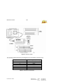
1
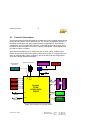
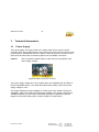
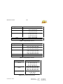
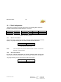
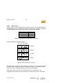
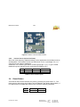
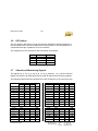
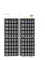
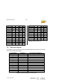
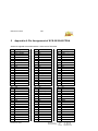
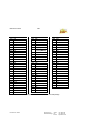
EVALXCS User Manual Board Module for FPGA Family ErSt Electronic GmbH Aeschstrasse 171 CH-8123 Ebmatingen Telefon Fax +41 1 980 61 44 +41 1 980 61 30 Internet http://www.erst.ch EVALXCS User Manual Manual: 2/2 EVALXCS EVALXCS Version 1.1 Version 1.2 August 1999 October 1999 This manual describes the technical properties and the usage of the following products: 5V versions: EVALXCS-20 EVALXCS-30 EVALXCS-40 Version 1.0 Version 1.0 Version 1.0 April 1999 April 1999 April 1999 3.3V versions: EVALXCS-20XL EVALXCS-30XL EVALXCS-40XL Version 1.0 Version 1.0 Version 1.0 April 1999 April 1999 April 1999 © ErSt Electronic GmbH, 1999 The ErSt Electronic GmbH reserves the right to make changes and improvements of the product without notice. Important Note: The EVALXCS board module has been designed and tested exclusively for the usage as a development tool. In particular, strong electromagnetic radiation may be produced. The ErSt Electronic GmbH does not undertake any liability for damages which may result from an improper use of this product. ErSt Electronic GmbH Aeschstrasse 171 CH-8123 Ebmatingen Telefon Fax +41 1 980 61 44 +41 1 980 61 30 Internet http://www.erst.ch EVALXCS User Manual 3/3 Contents: 1 Introduction .............................................................................. 5 2 Overview ................................................................................... 6 3 2.1 Key Features............................................................................... 6 2.2 Applications................................................................................ 6 2.3 Function Description.................................................................. 7 Technical Information.............................................................. 9 3.1 Power Supply ............................................................................. 9 3.2 FPGA Configuration................................................................ 11 3.2.1 Master Serial Mode....................................................................... 11 3.2.2 Slave Serial Mode ......................................................................... 11 3.2.2.1 Daisy Chain ........................................................................... 13 3.3 Clocks ....................................................................................... 14 3.3.1 External Clock .............................................................................. 14 3.3.1.1 Termination Resistors............................................................. 14 3.3.2 Internal Clock (Quarz Oscillator)................................................... 15 3.4 Reset Button ............................................................................. 15 3.5 LEDs......................................................................................... 16 3.6 DIP Switch................................................................................ 17 3.7 Stimuli and Monitoring Signals ............................................... 17 3.8 Dedicated Signals ..................................................................... 19 3.9 Stack Extension ........................................................................ 20 4 Literature ................................................................................ 21 5 Appendix A: Pin Assignment of XCS-20/30/40 FPGA............ 23 6 Appendix B: Schematic Diagram and PCB Layout ................ 25 ErSt Electronic GmbH Aeschstrasse 171 CH-8123 Ebmatingen Telefon Fax +41 1 980 61 44 +41 1 980 61 30 Internet http://www.erst.ch EVALXCS User Manual 4/4 Figures: Figure 1: Block diagram of the board module ...................................................... 7 Figure 2: Polarity of the power connector............................................................ 9 Figure 3: XChecker Cable ................................................................................. 12 Figure 4: External daisy chain connections........................................................ 13 Figure 5: Positions of the termination resistors.................................................. 15 Tables: Table 1: Supply voltages on ST1A ...................................................................... 10 Table 2: Supply voltages on ST2C...................................................................... 10 Table 3: Ground pins on all connectors ............................................................. 10 Table 4: Configuration Modes ........................................................................... 11 Table 5: Master Serial Mode ............................................................................. 11 Table 6: Slave Serial Mode ................................................................................ 11 Table 7: XChecker pin assignment ..................................................................... 12 Table 8: Pin assignment of the daisy chain connector ST4.................................. 13 Table 9: Clock sources ...................................................................................... 14 Table 10: External clock signals and termination resistors................................. 14 Table 11: Quarz oscillator signals ..................................................................... 15 Table 12: Reset signal ....................................................................................... 15 Table 13: LED signals ....................................................................................... 16 Table 14: DIP switch......................................................................................... 17 Table 15: General I/O signals............................................................................ 19 Table 16: Dedicated signals on connector ST1B................................................. 19 Table 17: Pin assignment of XCS-20/30/40 FPGA in PQ-208 package ............... 24 ErSt Electronic GmbH Aeschstrasse 171 CH-8123 Ebmatingen Telefon Fax +41 1 980 61 44 +41 1 980 61 30 Internet http://www.erst.ch EVALXCS User Manual 1 5/5 Introduction This manual describes the specific properties of the board module like power supply, FPGA configuration, clocks, reset, LEDs, DIP switches and I/O signals. Please take information about the FPGA from the Xilinx literature (see chapter 4 Literature). Online information can be found on the Xilinx websites: http://www.xilinx.com and http://www.support.xilinx.com Information about new products and new developments can be found on the ErSt Electronic Website: http://www.erst.ch If you have questions you may write to the following E-mail address: [email protected] ErSt Electronic GmbH Aeschstrasse 171 CH-8123 Ebmatingen Telefon Fax +41 1 980 61 44 +41 1 980 61 30 Internet http://www.erst.ch EVALXCS User Manual 2 Overview 2.1 ♦ ♦ ♦ ♦ ♦ ♦ ♦ ♦ ♦ ♦ ♦ ♦ ♦ 6/6 Key Features Xilinx FPGA Spartan XCS40/30/20 (5V) or XCS40XL/30XL/20XL (3.3V) in PQ208 package Header connector for Xchecker cable Header connector for external daisy chain connections SPROM for FPGA Master Serial Mode (DIL-8 package with socket) Quarz oscillator up to 80 MHz (DIL-8 or DIL-14 versions possible) Four position DIP switch for user configurations Push button for reset signal application or arbitrary usage Eight LED display for status messages 2 pole power connector for +5V/+3.3V power supply 4 layer PCB Clock signals may be equipped with termination resistors Stand alone usage of the board module possible The module has a standard size of 15cm x 10cm and a digital interface compatible with future products: 3x50 pole header connectors (2.54mm grid spacing) on each long side of the PCB The header connectors stand off from the top side of the PCB, the socket connectors from the bottom side Modules may be stacked to form a tower 2.2 ♦ ♦ ♦ ♦ ♦ ♦ ♦ ♦ ♦ ♦ Applications ASIC emulation Error monitoring and analysis Digital PLLs PWM controller Adaptive digitale filters Signal multiplexer Stimuli generators High speed encoder/decoder Memory controller Interface controller ErSt Electronic GmbH Aeschstrasse 171 CH-8123 Ebmatingen Telefon Fax +41 1 980 61 44 +41 1 980 61 30 Internet http://www.erst.ch EVALXCS User Manual 2.3 7/7 Function Description The board module EVALXCS-PQ208 is an ideal tool to test complex digital circuits during the early states of their development. The various configuration options of the Xilinx FPGAs allow the easy implementation of applications. The hardware configuration may be loaded via XChecker or SPROM. Almost all I/O pins of the FPGA are routed to header connectors, a total of 150 signals. These signals may be used as inputs or outputs. Several board modules may be stacked to form a tower, which enables one to realise circuits whose demand of gates is beyond the scope of a single FPGA. By using an external daisy chain connection, the whole stack can be configured at once with a single download operation. External clock sources Quarz oscillator with socket Quarz Oscillator Power supply connector Connector 2x50pol. VCC 7 SPROM 4 VCC >100 150 I/Os Done Spartan FPGA XCS40/30/20 PQ208 Header Connectors 2x50 poles XChecker Header connectors 2x50 poles 2 PGCK1 Daisy Chain PGCK2-4 SGCK1-3 Power LED 4 Four position DIP switch 8 Display with eight LEDs Done LED Reset Manual Reset Figure 1: Block diagram of the board module ErSt Electronic GmbH Aeschstrasse 171 CH-8123 Ebmatingen Telefon Fax +41 1 980 61 44 +41 1 980 61 30 Internet http://www.erst.ch EVALXCS User Manual 8/8 Seven clock sources can be used whereas one clock source is either the internal quarz oscillator or an external clock source. The quarz oscillator is inserted in a socket and can therefore be exchanged easily. Both DIL-8 and DIL-14 packages can be used. All clock signals may be terminated (parallel termination to ground) with termination resistors. These resistors can be mounted by the user on the bottom side of the PCB. A four position DIP switch is available for user defined purposes. There is also a push button whose primary intent is to serve as a reset button. Since this button is connected to a general I/O pin it may be used for arbitrary functions. An LED row with eight SIDELEDs is able to display status messages, error messages etc.. Figure 1 shows the above described function blocks. ErSt Electronic GmbH Aeschstrasse 171 CH-8123 Ebmatingen Telefon Fax +41 1 980 61 44 +41 1 980 61 30 Internet http://www.erst.ch EVALXCS User Manual 3 3.1 9/9 Technical Information Power Supply The power supply of a single module or a whole stack comes from the power connector ST5. The negative pole is on the side of the power LED, the screw of the positive pole is marked with red color. Within a stack any power connector can be used since all boards are connected together over the header connectors. Caution: Use only board modules within a stack which are specified for the same supply voltage! Figure 2: Polarity of the power connector The power supply voltage is 5V for modules which are equipped with an FPGA of the XCS-20/30/40 family. If the XCS-20XL/30XL/40XL family is used, the power supply voltage is 3.3V. The supply voltages are also available on certain pins of the header connectors. verfügbar. Table 1 and Table 2 list the supply voltages. Only certain voltages are available depending on the used FPGA family (Spartan or SpartanXL) and the usage of the board module (with or without usage of a base board). ErSt Electronic GmbH Aeschstrasse 171 CH-8123 Ebmatingen Telefon Fax +41 1 980 61 44 +41 1 980 61 30 Internet http://www.erst.ch EVALXCS User Manual 10/10 Signal Name +5V +3.3V GND +12V -12V Connector Pins on ST1A 1, 2, 3, 4, 5 36, 37, 38, 39, 40 6, 7, 8, 9, 10 41, 42, 43, 44, 45 11, 12, 13, 14, 15 21, 22, 23, 24, 25 31, 32, 33, 34, 35 46, 47, 48, 49, 50 16, 17, 18, 19, 20 26, 27, 28, 29, 30 Table 1: Supply voltages on ST1A Signal Name +5V +3.3V GND +12V -12V Connector Pins on ST2C 111, 112, 113, 114, 115 146, 147, 148, 149, 150 106, 107, 108, 109, 110 141,142, 143, 144,145 101, 102, 103, 104, 105 116, 117,118, 119, 120 126, 127, 128, 129, 130 136, 137,138, 139, 140 131, 132, 133, 134, 135 121, 122, 123, 124, 125 Table 2: Supply voltages on ST2C Connector ST1A ST2C ST1B Pin Numbers 11, 12, 13, 14, 15 21, 22, 23, 24, 25 31, 32, 33, 34, 35 46, 47, 48, 49, 50 101, 102, 103, 104, 105 116, 117,118, 119, 120 126, 127, 128, 129, 130 136, 137,138, 139, 140 51, 53, 55, 57, 59 61, 63, 65, 67 72, 75, 78 Table 3: Ground pins on all connectors ErSt Electronic GmbH Aeschstrasse 171 CH-8123 Ebmatingen Telefon Fax +41 1 980 61 44 +41 1 980 61 30 Internet http://www.erst.ch EVALXCS User Manual 3.2 11/11 FPGA Configuration There are two options to configure the FPGA. The following table shows the possible modes and the jumper settings of J1 and J2: Mode Data (J1) Master Serial inserted Slave Serial not inserted Mode (J2) not inserted inserted CCLK Daten Output Bit serial Input Bit serial Comment SPROM (DIL-8) XChecker (PC) Table 4: Configuration Modes 3.2.1 Master Serial Mode The board module contains an 8 pin DIL socket for Serial Configuration PROMs (SCPs). The jumper settings for the master serial mode are as follows: J1 (Data) inserted J2 (Mode) not inserted Table 5: Master Serial Mode Note: 3.2.2 The XChecker cable must be disconnected to avoid a contention between CCLK and DIN! Slave Serial Mode For this form of FPGA configuration you need an XChecker cable from XILINX, which serves as interface between the board module and the PC, see Figure 2. The jumper settings for the slave serial mode are as follows: J1 (Data) not inserted J2 (Mode) inserted Table 6: Slave Serial Mode ErSt Electronic GmbH Aeschstrasse 171 CH-8123 Ebmatingen Telefon Fax +41 1 980 61 44 +41 1 980 61 30 Internet http://www.erst.ch EVALXCS User Manual 12/12 Figure 3: XChecker Cable The following table shows the pin assignment of the header connector ST3: ST3 (Header Connector) 1 2 3 4 5 6 7 XChecker (Connector 1) PROG\ DONE INIT\ CCLK DIN VCC GND Table 7: XChecker pin assignment ErSt Electronic GmbH Aeschstrasse 171 CH-8123 Ebmatingen Telefon Fax +41 1 980 61 44 +41 1 980 61 30 Internet http://www.erst.ch EVALXCS User Manual 3.2.2.1 13/13 Daisy Chain A whole stack may be configured with a single download. To accomplish this the individual layers must be connected in form of a daisy chain. External connections of appropriate pins of connector ST4 perform this task (see Table 8). ST4 (Connector) 1 2 3 4 Pin Name dup din dout ddown Table 8: Pin assignment of the daisy chain connector ST4 Use the following connection scheme: dup din dout ddown Level 4 Level 3 Level 2 Level 1 Figure 4: External daisy chain connections The easiest way to make the connections dup-din and dout-ddown is to insert a jumper. However, these connections are only needed if the stack is connected to a main board and if the configuration data comes from the main board. If the main board is not used you need only the dout-din connections. The configuration bit streams are then feeded to the lowest level (SCP or XChecker). ErSt Electronic GmbH Aeschstrasse 171 CH-8123 Ebmatingen Telefon Fax +41 1 980 61 44 +41 1 980 61 30 Internet http://www.erst.ch EVALXCS User Manual 3.3 14/14 Clocks The seven clock signals pgck1 to pgck4 and sgck1 to sgck3 are routed to the header connectors where pgck1 may be connected optionally to the internal quarz oscillator, see Table 9. Source Quarz Oscillator Ext. Clock (pin 52 of ST1B) J3 (CLK int.) inserted not inserted J4 (CLK ext.) not inserted inserted Table 9: Clock sources 3.3.1 External Clock The assignment of the clock signals to the connectors pins is shown in the following table: Signal Name Connector ST1B FPGA Pin Termination Resistor pgck1 52 2 R18 pgck2 54 55 R19 pgck3 56 108 R20 pgck4 58 160 R21 sgck1 60 207 R22 sgck2 62 49 R23 sgck3 64 102 R24 sgck4/dout not connected 154 Table 10: External clock signals and termination resistors 3.3.1.1 Termination Resistors The clock signals pgck1 to pgck4 and sgck1 to sgck3 may be terminated with resistors (R18 to R24) which are connected immediately from the FPGA pin to ground. These resistors form a parallel termination. The values of the resistors should match the impedance of the circuit board trace which has a nominal value of 100 Ohms. Please consider the maximal output current capability of the clock source! The resistors (SMD, size 0805) can be soldered to the board directly beneath the FPGA on the bottom side of the PCB. Figure 5 shows the positions: ErSt Electronic GmbH Aeschstrasse 171 CH-8123 Ebmatingen Telefon Fax +41 1 980 61 44 +41 1 980 61 30 Internet http://www.erst.ch EVALXCS User Manual 15/15 Figure 5: Positions of the termination resistors 3.3.2 Internal Clock (Quarz Oscillator) Since the clock frequency depends strongly on the application the oscillator must be exchangeable. The oscillator socket can hold DIL-8 or DIL-14 packages. Pin 1 is common for both types of packages. Oscillators of the VCXO type need a control signal at pin 1 (Uc). To get a closed feedback loop this signal must be connected (via FPGA) to Uout. Osz. Uc Uout Net Name ch_a_9 pgck1 FPGA Pin 27 2 FPGA I/O Output Clock Input Table 11: Quarz oscillator signals 3.4 Reset Button A functional reset can be issued at any time by pressing the push button T1. The reset signal is active high and needs to be considered in the design appropriately. If no reset function is needed the button may be used for arbitrary purposes. Button T1 Net Name reset FPGA Pin 56 Table 12: Reset signal ErSt Electronic GmbH Aeschstrasse 171 CH-8123 Ebmatingen Telefon Fax +41 1 980 61 44 +41 1 980 61 30 Internet http://www.erst.ch EVALXCS User Manual 16/16 Note 1: A manual reset initialises the internal circuits of the FPGA (registers, counters, finite state machines etc.) and must be implemented in the design appropriately. Note 2: Do not press the reset button during the download of a bit stream since this may interfere with the HDC function! Note 3: When used in a stack, all HDC pins of all FPGAs are connected in parallel. Unconfigured FPGAs tie this pin to high level and act therefore like a pressed reset button. Make sure to configure this pin as an input if the reset function is desired! 3.5 LEDs The eight LEDs D3 to D10 are intended as optical indicators for the display of status information. D2 is connected to the DONE pin of the FPGA and D1 serves as power indicator LED. The DONE LED turns on at the end of a successful bit stream download. The LEDs D3 to D10 turn on whenever the corresponding FPGA output is low. The following table shows the assignment to the FPGA pins: LED Net Name FPGA Pin D3 ch_a_1 15 D4 ch_a_2 17 D5 ch_a_3 19 D6 ch_a_4 20 D7 ch_a_5 21 D8 ch_a_6 22 D9 ch_a_7 23 D10 ch_a_8 24 Table 13: LED signals Note: If the board module is used within a stack the LEDs of all levels are connected in parallel. If one LED is driven by the FPGA the LEDs of the other levels are driven also. The maximal output current of 20mA of an FPGA port is sufficient for up to four levels. If more than four levels are used, the current limiting resistors of the LEDs of the remaining levels must be removed. ErSt Electronic GmbH Aeschstrasse 171 CH-8123 Ebmatingen Telefon Fax +41 1 980 61 44 +41 1 980 61 30 Internet http://www.erst.ch EVALXCS User Manual 3.6 17/17 DIP Switch The four position DIP switch S1 can be used for application specific purposes. In the On position the connected FPGA pin is tied to ground. In the Off position the connected FPGA pin is pulled to VCC via a resistor. The assignment of the switches to the FPGA pins is as follows: Switch Net Name FPGA Pin 1 sw1 149 2 sw2 150 3 sw3 151 4 sw4 152 Table 14: DIP switch 3.7 Stimuli and Monitoring Signals The signals ch_a_1 to ch_a_50, ch_b_1 to ch_b_50 and r_1 to r_50 are routed to header connectors. All these pins may be used as stimuli and monitoring signals. The following table shows the assignment of the FPGA pins to the connector pins: Net Name r_1 r_2 r_3 r_4 r_5 r_6 r_7 r_8 r_9 r_10 r_11 r_12 r_13 r_14 r_15 r_16 r_17 r_18 FPGA Connector ST1C ST2B ST2A Pin 101 14 102 12 103 11 104 10 105 9 106 8 107 5 108 4 109 3 110 206 111 205 112 204 113 203 114 202 115 201 116 200 117 199 118 198 ErSt Electronic GmbH r_19 r_20 r_21 r_22 r_23 r_24 r_25 r_26 r_27 r_28 r_29 r_30 r_31 r_32 r_33 r_34 r_35 r_36 r_37 r_38 119 120 121 122 123 124 125 126 127 128 129 130 131 132 133 134 135 136 137 138 Aeschstrasse 171 CH-8123 Ebmatingen 197 196 194 193 191 190 189 188 187 186 185 184 181 180 179 178 177 176 175 174 Telefon Fax +41 1 980 61 44 +41 1 980 61 30 Internet http://www.erst.ch EVALXCS User Manual r_39 r_40 r_41 r_42 r_43 r_44 r_45 r_46 r_47 r_48 r_49 r_50 ch_a_1 ch_a_2 ch_a_3 ch_a_4 ch_a_5 ch_a_6 ch_a_7 ch_a_8 ch_a_9 ch_a_10 ch_a_11 ch_a_12 ch_a_13 ch_a_14 ch_a_15 ch_a_16 ch_a_17 ch_a_18 ch_a_19 ch_a_20 ch_a_21 ch_a_22 ch_a_23 ch_a_24 ch_a_25 ch_a_26 ch_a_27 ch_a_28 ch_a_29 ch_a_30 18/18 139 140 141 142 143 144 145 146 147 148 149 150 ErSt Electronic GmbH 51 52 53 54 55 56 57 58 59 60 61 62 63 64 65 66 67 68 69 70 71 72 73 74 75 76 77 78 79 80 172 171 169 168 167 166 165 164 163 162 161 159 15 17 19 20 21 22 23 24 27 28 29 30 31 32 34 35 36 37 39 40 41 42 43 44 45 46 47 48 57 58 ch_a_31 ch_a_32 ch_a_33 ch_a_34 ch_a_35 ch_a_36 ch_a_37 ch_a_38 ch_a_39 ch_a_40 ch_a_41 ch_a_42 ch_a_43 ch_a_44 ch_a_45 ch_a_46 ch_a_47 ch_a_48 ch_a_49 ch_a_50 ch_b_1 ch_b_2 ch_b_3 ch_b_4 ch_b_5 ch_b_6 ch_b_7 ch_b_8 ch_b_9 ch_b_10 ch_b_11 ch_b_12 ch_b_13 ch_b_14 ch_b_15 ch_b_16 ch_b_17 ch_b_18 ch_b_19 ch_b_20 ch_b_21 ch_b_22 Aeschstrasse 171 CH-8123 Ebmatingen 81 82 83 84 85 86 87 88 89 90 91 92 93 94 95 96 97 98 99 100 1 2 3 4 5 6 7 8 9 10 11 12 13 14 15 16 17 18 19 20 21 22 59 61 62 63 64 65 67 68 69 70 72 73 74 75 76 80 81 82 83 84 85 87 88 89 90 92 93 94 95 96 97 98 99 100 101 107 109 110 111 112 113 114 Telefon Fax +41 1 980 61 44 +41 1 980 61 30 Internet http://www.erst.ch EVALXCS User Manual 19/19 ch_b_23 ch_b_24 ch_b_25 ch_b_26 ch_b_27 ch_b_28 ch_b_29 ch_b_30 ch_b_31 ch_b_32 ch_b_33 ch_b_34 ch_b_35 ch_b_36 ch_b_37 ch_b_38 3.8 23 24 25 26 27 28 29 30 31 32 33 34 35 36 37 38 115 116 117 119 120 122 123 124 125 126 127 128 129 132 133 134 ch_b_39 ch_b_40 ch_b_41 ch_b_42 ch_b_43 ch_b_44 ch_b_45 ch_b_46 ch_b_47 ch_b_48 ch_b_49 ch_b_50 39 40 41 42 43 44 45 46 47 48 49 50 135 136 137 138 139 141 142 144 145 146 147 148 Table 15: General I/O signals Dedicated Signals The header connector ST1B contains some dedicated signals which are used as clock and configuration signals. Signal Name pgck_ext pgck2 pgck3 pgck4 sgck1 sgck2 sgck3 tdi tck tms tdo hdc ldc dup ddown ST1B Pin 52 54 56 58 60 62 64 68 69 70 71 73 74 76 77 Connected to FPGA pin 2 (over J2) 55 108 160 207 49 102 6 7 16 157 56 60 N/A (goes to pin 1 of ST4) N/A (goes to pin 4 of ST4) Table 16: Dedicated signals on connector ST1B ErSt Electronic GmbH Aeschstrasse 171 CH-8123 Ebmatingen Telefon Fax +41 1 980 61 44 +41 1 980 61 30 Internet http://www.erst.ch EVALXCS User Manual 3.9 20/20 Stack Extension When several board modules are stacked the signal direction of I/O pins of different levels must be choosen very carefully. Short circuits between the FPGAs may result in damages or shortens their life. Unconfigured pins of the FPGA are in a high impedance state. During the assembly of the stack you should pay attention to the fact that the pins of one module are aligned exactly with the holes of the sockets of the other module. A good possibility to accomplish this is the usage of two pieces of a prototyping board. Each of these pieces should have three rows with 50 holes. Before the assembly these pieces are slided up to the ends of the connector pins. Thereby, the pin ends keep their positions. To disassemble a stack we recommend the usage of pliers which are used to remove locking rings. The claws of the pliers should be covered with plastic or rubber tubes to prevent damages on the boards. The modules are then separated easily by repeated application of gentle pressure with the pliers on all four corners. ErSt Electronic GmbH Aeschstrasse 171 CH-8123 Ebmatingen Telefon Fax +41 1 980 61 44 +41 1 980 61 30 Internet http://www.erst.ch EVALXCS User Manual 4 21/21 Literature The following list is an excerpt from the Xilinx literature concerning the Spartan FPGA family. The correspondent PDF files may be downloaded directly from http://www.xilinx.com/apps/spartapp.htm or be requested from a Xilinx distributor. Application Notes XAPP120: How Spartan Series FPGAs Compete for Gate Array Production XAPP125: Conserving Power With Auto Power Down Mode in SpartanXL FPGAs XAPP124: Using Manual Power Down Mode With SpartanXL FPGAs XAPP123: Using Three-State Enable Registers in XLA, XV, and SpartanXL FPGAs XAPP099: How to Design Today for the Upcoming SpartanXL FPGA Family XAPP088: I/O Characteristics of the ’XL FPGAs SelectRAM Memory XAPP065: Edge-Triggered and Dual-Port RAM Capability XAPP057: Using SelectRAM Memory in FPGAs XAPP053: Implementing FIFOs in RAM XAPP051: Synchronous and Asynchronous FIFO Designs XAPP052: Efficient Shift Registers, LFSR Counters, and Long PseudoRandom Sequence Generators Carry Logic XAPP013: Using the Dedicated Carry Logic XAPP023: Accelerating Loadable Counters XAPP018: Estimating the Performance of Adders and Counters XAPP014: Ultra-Fast Synchronous Counters XAPP027: Implementing State Machines in FPGA Devices Configuration XAPP126: Data Generation and Configuration for Spartan Series FPGAs XAPP098: The Low-Cost, Efficient Serial Configuration of Spartan FPGAs XAPP122: The Express Configuration of SpartanXL FPGAs XAPP091: Configuring Mixed FPGA Daisy Chains XAPP015: Using the Readback Capability XAPP017: Boundary Scan in Xilinx Devices Application Briefs ErSt Electronic GmbH Aeschstrasse 171 CH-8123 Ebmatingen Telefon Fax +41 1 980 61 44 +41 1 980 61 30 Internet http://www.erst.ch EVALXCS User Manual 22/22 XBRF001: SelectRAM: Flexibility with Speed XBRF002: Low Power Benefits: Overview XBRF003: SelectRAM: Maximum Configurability XBRF007: Xilinx FPGAs: The Best Choice for Delivering Logic Cores XBRF014: A Simple Method of Estimating Power in FPGAs Data Book Spartan and SpartanXL Series Datasheet v1.4, 1/99 Spartan Serial Configuration PROMs Datasheet v1.2, 9/98 Xcell Articles The 3.3V SpartanXL FPGA Series Invades New Territory with High Speed and Low Cost Q4 ’98 FPGAs Can Be an Effective Alternative to Mask Gate Arrays Q4 ’98 New Spartan -4 Devices for High Speed Applications Q3 ’98 Esaote Biomedica: A Spartan Success Story Q3 ’98 The Low Cost PCI Solution Q3 ’98 Spartan Series Takes the Lead with Low Power Q2 ’98 Designing with the Spartan Series FPGAs Q2 ’98 Introducing the New Spartan FPGA Family for Low Cost Applications Q1 ’98 Xilinx DSP LogiCORE Advantages Q3 ’97 SelectRAM Memory: Advantages and Uses Q3 ’96 Synchronous RAM Improves System Speed Q4 ’95 Synchronous RAM Timing Q4 ’95 Advanced Carry Logic Techniques Q2 ’96 ErSt Electronic GmbH Aeschstrasse 171 CH-8123 Ebmatingen Telefon Fax +41 1 980 61 44 +41 1 980 61 30 Internet http://www.erst.ch EVALXCS User Manual 5 23/23 Appendix A: Pin Assignment of XCS-20/30/40 FPGA Active low signals are marked with a \ at the end of the name. Pin 1 2 3 4 5 6 7 8 9 10 11 12 13 14 15 16 17 18 19 20 21 22 23 24 25 26 27 28 29 30 31 32 33 34 35 36 37 Description GND I/O, PGCK1 I/O I/O I/O I/O, TDI I/O, TCK I/O I/O I/O I/O I/O GND I/O I/O I/O, TMS I/O VCC I/O I/O I/O I/O I/O I/O GND VCC I/O I/O I/O I/O I/O I/O VCC I/O I/O I/O I/O ErSt Electronic GmbH 38 39 40 41 42 43 44 45 46 47 48 49 50 51 52 53 54 55 56 57 58 59 60 61 62 63 64 65 66 67 68 69 70 71 72 73 74 75 GND I/O I/O I/O I/O I/O I/O I/O I/O I/O I/O I/O, SGCK2 Don‘ t connect GND MODE VCC Don‘ t connect I/O, PGCK2 I/O(HDC) I/O I/O I/O I/O(LDC\) I/O I/O I/O I/O I/O GND I/O I/O I/O I/O VCC I/O I/O I/O I/O 76 77 78 79 80 81 82 83 84 85 86 87 88 89 90 91 92 93 94 95 96 97 98 99 100 101 102 103 104 105 106 107 108 109 110 111 112 113 Aeschstrasse 171 CH-8123 Ebmatingen I/O I/O(INIT\) VCC GND I/O I/O I/O I/O I/O I/O VCC I/O I/O I/O I/O GND I/O I/O I/O I/O I/O I/O I/O I/O I/O I/O I/O, SGCK3 GND DONE VCC PROGRAM\ I/O I/O, PGCK3 I/O I/O I/O I/O I/O Telefon Fax +41 1 980 61 44 +41 1 980 61 30 Internet http://www.erst.ch EVALXCS User Manual 114 115 116 117 118 119 120 121 122 123 124 125 126 127 128 129 130 131 132 133 134 135 134 137 138 139 140 141 142 143 144 145 146 I/O I/O I/O I/O GND I/O I/O VCC I/O I/O I/O I/O I/O I/O I/O I/O VCC GND I/O I/O I/O I/O I/O I/O I/O I/O VCC I/O I/O GND I/O I/O I/O 24/24 147 148 149 150 151 152 153 154 155 156 157 158 159 160 161 162 163 164 165 166 167 168 169 170 171 172 173 174 175 176 177 178 I/O I/O I/O I/O I/O I/O I/O(DIN) I/O, SGCK4(DOUT) CCLK VCC O, TDO GND I/O I/O, PGCK4 I/O I/O I/O I/O I/O I/O I/O I/O I/O GND I/O I/O VCC I/O I/O I/O I/O I/O 179 180 181 182 183 184 185 186 187 188 189 190 191 192 193 194 195 196 197 198 199 200 201 202 203 204 205 206 207 208 I/O I/O I/O GND VCC I/O I/O I/O I/O I/O I/O I/O I/O VCC I/O I/O GND I/O I/O I/O I/O I/O I/O I/O I/O I/O I/O I/O I/O, SGCK1 VCC Table 17: Pin assignment of XCS-20/30/40 FPGA in PQ-208 package ErSt Electronic GmbH Aeschstrasse 171 CH-8123 Ebmatingen Telefon Fax +41 1 980 61 44 +41 1 980 61 30 Internet http://www.erst.ch EVALXCS User Manual 6 25/25 Appendix B: Schematic Diagram and PCB Layout The following pages show some technical details of the board: ♦ ♦ ♦ Top overlay silk screen Layout (signal layers) Schematic diagram ErSt Electronic GmbH Aeschstrasse 171 CH-8123 Ebmatingen Telefon Fax +41 1 980 61 44 +41 1 980 61 30 Internet http://www.erst.ch