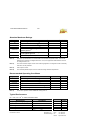
1
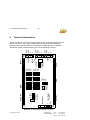
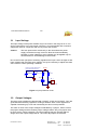
Power Module PWR3 User Manual
User Manual
ErSt Electronic GmbH
Zürichstrasse 111
CH-8123 Ebmatingen
Phone
Fax
+41 1 980 61 44
+41 1 980 61 30
Internet
http://www.erst.ch
PWR3 User Manual
Manual Version:
2/12
PWR3
Version 1.0
July 1999
This manual describes the technical properties and the usage of the following
products:
Power Module PWR3
Version 1.0
July 1999
© ErSt Electronic GmbH, 1999
The ErSt Electronic GmbH reserves the right to make changes and improvements
of the product without notice.
Important Note:
The power module PWR3 has been designed and tested exclusively for the
usage as a development tool. In particular, strong electromagnetic radiation
may be produced. The ErSt Electronic GmbH does not undertake any
liability for damages which may result from an improper use of this product.
ErSt Electronic GmbH
Zürichstrasse 111
CH-8123 Ebmatingen
Phone
Fax
+41 1 980 61 44
+41 1 980 61 30
Internet
http://www.erst.ch
PWR3 User Manual
3/12
Contents:
1
Introduction ................................................................................. 4
2
Overview....................................................................................... 5
3
2.1
Key Features...................................................................................5
2.2
Function Description .....................................................................7
Technical Information ................................................................ 8
3.1
Input Voltage..................................................................................9
3.2
Output Voltages .............................................................................9
3.3
Reference Voltages.......................................................................11
3.4
Indicator LEDs.............................................................................12
Figures:
Figure 1: Block diagram of the power module PWR3 ............................................. 5
Figure 2: Component placement overview .............................................................. 8
Figure 3: Input protection circuit ............................................................................ 9
Figure 4: Reference voltage generation................................................................. 12
Tables:
Table 1: Configuration of the output voltages ....................................................... 10
Table 2: Potentiometer for variable setting. .......................................................... 10
Table 3: Pin numbers and signals on the header connectors................................. 11
ErSt Electronic GmbH
Zürichstrasse 111
CH-8123 Ebmatingen
Phone
Fax
+41 1 980 61 44
+41 1 980 61 30
Internet
http://www.erst.ch
Power Module PWR3 User Manual
1
4/12
Introduction
The ongoing miniaturisation of integrated circuits leads to lower supply voltages.
This is due to two reasons. First, the dielectric streng of the insulator layers is
limited. Second, the power dissipation can be minimised drastically (dynamic power
dissipation is proportional to the square of the supply voltage).
The commonly used technologies work with 5V and 3.3V where the structure size
goes down to 0.35µm. Already today, 0.25µm processes are state of the art and in
the future the semiconductor manufacturers will be able to work with 0.18µm and
0.13µm structure sizes. The supply voltages will follow this trend and reach 2.5V,
1.8V and 1.3V.
Integrated circuits of different technologies with different supply voltages must work
together in the same system. The implication of this is, that a single device can not
longer work with a single supply voltage. Internal supplies and output driver
supplies are separate from each other.
The power module PWR3 generates three regulated voltages in the range of 1.3 to
5V to ease the use of future digital integrated circuits. In addition, eight reference
voltages for the support of multistandard I/Os are provided.
Information about new products and new developments can be found on the
ErSt Electronic Website:
http://www.erst.ch
If you have questions you may write to the following email address:
[email protected]
We will answer as soon as possible, usually within one or two days.
ErSt Electronic GmbH
Zürichstrasse 111
CH-8123 Ebmatingen
Phone
Fax
+41 1 980 61 44
+41 1 980 61 30
Internet
http://www.erst.ch
Power Module PWR3 User Manual
2
2.1
•
•
•
•
•
•
•
•
•
•
•
•
•
5/12
Overview
Key Features
Input power supply range 6-14V
Switching regulator for VCCINT (1.8V/2.5V/3.3V/5V/Uvar)
Switching regulator for VCCO (1.5V/2.5V/3.3V/5V/Uvar)
Switching regulator for VCCOPT (1.8V/2.5V/3.3V/5V/Uvar)
Output voltages selectable with jumper
Uvar is user adjustable in the range 1.3-5.2V
Switching regulators are protected against short circuits and thermal overload
Max. 4A load current for all output voltages
All output voltages available on header connectors and power connectors
Output power sufficient for up to three board modules
6 reference voltages (0.75V, 0.8V, 1V, 1.125V, 1.32V and 1.5V) for 8 I/O banks
selectable with DIP switch matrix
May be stacked with EVALXCV
Board size 86mm x 150mm
Connector
VREF
6
VCCO
Select
1.8V/2.5V/3.3V/5V/Uvar
Connector
Select
1.8V/2.5V/3.3V/5V/Uvar
VCCOPT
Select
1.5V/2.5/3.3V/5V/Uvar
DIP-Switch Matrix
8
Header
Connector
VCCINT
Connector
Power Supply
6-14V
Figure 1: Block diagram of the power module PWR3
ErSt Electronic GmbH
Zürichstrasse 111
CH-8123 Ebmatingen
Phone
Fax
+41 1 980 61 44
+41 1 980 61 30
Internet
http://www.erst.ch
Power Module PWR3 User Manual
6/12
Absolute Maximum Ratings
Symbol
VIN
IOUTVCCINT
IOUTVCCO
IOUTVCCOPT
TSHORTOUT
TSHORTREF
TAMB
Description
1)
Input voltage
2)
Output current for VCCINT
2)
Output current for VCCO
2)
Output current for VCCOPT
Duration of output voltage short circuit
3)
against ground
Duration of reference voltage short
circuit against ground
4)
Ambient temperature
Unit
V
A
A
A
-0.3 ... 14
4
4
4
Continuous
Continuous
o
0 ... 70
C
Note 1):
The input is protected with an inverse diode and a transient suppressor diode. The inverse
diode starts to conduct at voltages lower than –0.3V, the suppressor diode starts to conduct
for voltages above 14V.
Note 2):
This is the maximal output current of the switching regulator. The regulator circuit is thermally
and short circuits protected.
Note 3):
One output at a time.
Note 4):
The maximal possible output current is reduced at high ambient temperatures.
Recommended Operating Conditions
Symbol
VIN
IOUTVCCINT
IOUTVCCO
IOUTVCCOPT
IOUTREF
TAMB
Note 1):
Description
Input voltage
1)
Output current for VCCINT
1)
Output current for VCCO
1)
Output current for VCCOPT
Output current of a reference voltage
Ambient temperature
6 ... 12
3
3
3
10
0 ... 40
Unit
V
A
A
A
mA
o
C
Continuous operation without additional cooling at 25 oC.
Typical Performance
VIN = 10V, Ta = 25 oC unless otherwise noted
Description
Output ripple voltage (Vp-p)
Quiscent current
Efficiency
Efficiency
Efficiency
ErSt Electronic GmbH
Condition
IOUT = 4A
VOUT = 2.5V, IOUT = 4A
VOUT = 3.3V, IOUT = 4A
VOUT = 5V, IOUT = 4A
Zürichstrasse 111
CH-8123 Ebmatingen
25
75
75
78
83
Unit
mV
mA
%
%
%
Phone
Fax
+41 1 980 61 44
+41 1 980 61 30
Internet
http://www.erst.ch
Power Module PWR3 User Manual
2.2
7/12
Function Description
The power module PWR3 generates three regulated output voltages and eight
reference voltages from a single unregulated power supply. The input supply
voltage can be in the range from 6V to 14V. An inverse diode and a transient
suppressor diode in conjunction with a fuse protect the module from inverted supply
voltages and voltage transients.
The output voltages are generated with switching regulators working with 500kHz
operating frequency and having an output current capability of 4A. They are
thermally and short circuit protected. All output voltages are configureable with
jumpers. Four settings (5V, 3.3V, 2.5V and 1.8V resp. 1.5V) are fix, a fifth setting is
adjustable with a trim potentiometer. The three output voltages are available on
header and power connectors. Each of the power connectors allows the connection
of four wires, two for ground and two for output power.
Each of the eight reference voltages may be selected with DIP switches among six
fixed voltages (0.75V, 0.8V, 1.0V, 1.125V, 1.32V and 1.5V). The reference voltages
are also routed to the header connectors, buffered with a source follower.
Four LEDs show the state of the three output voltages and the power supply. The
three LEDs which correspond to the three output voltages are driven by operational
amplifiers connected to the voltage feedback input of the switching regulators. The
reason for this is, that the output voltage may be well below the minimal forward
voltage of an LED.
ErSt Electronic GmbH
Zürichstrasse 111
CH-8123 Ebmatingen
Phone
Fax
+41 1 980 61 44
+41 1 980 61 30
Internet
http://www.erst.ch
Power Module PWR3 User Manual
3
8/12
Technical Information
VCCO
38 39
0.75V
0.80V
1.00V
1.125V
1.32V
1.50V
1
2
3
4
5
6
GND
VCCINT
12 13
1
+
Input Supply
6-12V
GND
VCCINT
Selection
Fuse 4A fast
1
2
3
4
5
6
VCCOPT
Selection
1
2
3
4
5
6
adjust
1.8V
2.5V
3.3V
5V
1
2
3
4
5
6
VREF7
VREF5
VREF4
VREF6
50
+
+
GND
VCCO
Selection
VCCO
GND
+
+
GND
+
+
VCCINT
GND
GND
GND
0.75V
0.80V
1.00V
1.125V
1.32V
1.50V
VREF3
1
2
3
4
5
6
1
2
3
4
5
6
1
2
3
4
5
6
1
2
3
4
5
6
VREF2
VREF1
VREF0
25
12 13
GND
1
adjust
1.8V
2.5V
3.3V
5V
VCCOPT
5V
3.3V
2.5V
1.5V
adjust
VREF 0 - 7
VCCOPT
Figure 2 shows an overview of the placement of key components like input and
output connectors, fuse, output voltage selection jumpers with adjustment
potentiometers and DIP switches for reference voltage selection. A detailed
description of each of these items is given in the following sections.
Figure 2: Component placement overview
ErSt Electronic GmbH
Zürichstrasse 111
CH-8123 Ebmatingen
Phone
Fax
+41 1 980 61 44
+41 1 980 61 30
Internet
http://www.erst.ch
Power Module PWR3 User Manual
3.1
9/12
Input Voltage
The input voltage of the power module may be choosen in the range of 6V to 14V
and is connected to a two pole power connector. An inverse diode and a transient
suppressor diode in conjunction with a fuse protect the module.
Caution:
The fuse protects the module only in the case where the power
supply can deliver enough current to blow the fuse immediately.
Normally, inverse voltages or over voltages may be applied only for
short durations to avoid damage to the module.
Due to the function principle of switching regulators the input current is higher at low
input voltages than at higher input voltages. It may be necessary to adjust the value
of the fuse for certain operating conditions.
Inverse Voltage Protection
Overvoltage Protection
D13
30BQ040
D11
SMCJ15A
VPWR
R65
510E
F1
4A fast
D12
KL1
Power Indicator
1
2
Input 6-14V
Figure 3: Input protection circuit
3.2
Output Voltages
The three ouput voltages are denoted with VCCINT, VCCO and VCCOPT. They are
generated with switching regulators working at 500kHz. Each of the regulators is
capable of delivering up to 4A and is thermally and short circuit protected.
The value of each of the output voltages is selectable by a jumper. Table 1 shows
the jumper settings and the resulting output voltage values. Only one jumper must
be set at a time. During operation, the jumper settings may be changed without
danger since the output voltage falls to 1.2V when all jumpers are removed.
ErSt Electronic GmbH
Zürichstrasse 111
CH-8123 Ebmatingen
Phone
Fax
+41 1 980 61 44
+41 1 980 61 30
Internet
http://www.erst.ch
Power Module PWR3 User Manual
Caution:
10/12
Never insert more than one jumper at the same time since the output
voltage may then rise well above 5V, limited by the input voltage level
only.
Jumper
J6
J7
J8
J9
J10
VCCINT
5V
3.3V
2.5V
1.8V
variable
Jumper
J11
J12
J13
J14
J15
VCCO
5V
3.3V
2.5V
1.5V
variable
Jumper
J1
J2
J3
J4
J5
VCCOPT
5V
3.3V
2.5V
1.8V
variable
Table 1: Configuration of the output voltages
In the variable setting, the output voltages are adjustable with a trim potentiometer
(see Table 2) in the range from 1.3V to 5.2V.
Note:
The factory settings of the variable output voltages is undefined and
must be adjusted to a reasonable value by the user before
connecting anything to the output!
Potentiometer
R19
R18
R17
Output voltage
VCCINT
VCCO
VCCOPT
Table 2: Potentiometer for variable setting.
The output voltages are routed to power connectors and to header connectors. The
naming and positioning of the signals on the header connectors corresponds with
according connectors on board modules. Table 3 shows the pins and signals on the
header connectors. Also refer to Figure 2.
ErSt Electronic GmbH
Zürichstrasse 111
CH-8123 Ebmatingen
Phone
Fax
+41 1 980 61 44
+41 1 980 61 30
Internet
http://www.erst.ch
Power Module PWR3 User Manual
Connector
ST1
ST2
11/12
Pin Number
1 to 12
13 to 25
26 to 42
43
44
45
46
47
48
49
50
1 to 12
13 to 38
39 to 50
Signal Name
VCCOPT
GND
Reserved
VREF0
VREF1
VREF2
VREF3
VREF4
VREF5
VREF6
VREF7
VCCINT
GND
VCCO
Table 3: Pin numbers and signals on the header connectors
3.3
Reference Voltages
Figure 4 shows the circuit which generates the reference voltages. Eight reference
voltages may be selected among six fixed voltages (0.75V, 0.8V, 1.0V, 1.125V,
1.32V und 1.5V) by means of DIP switches. All reference voltages are derived with
resistive voltage dividers from a 2.5V reference.
Note:
Only one switch of each six position switch should be in the on
position. If two or more switches are in the on position, the voltage
dividers are connected in parallel and the reference voltage assumes
a wrong value.
The voltage dividers are buffered with an OpAmp (source follower). The output
current of each reference voltage (VREF0 to VREF7) may be up to ca. 10mA.
ErSt Electronic GmbH
Zürichstrasse 111
CH-8123 Ebmatingen
Phone
Fax
+41 1 980 61 44
+41 1 980 61 30
Internet
http://www.erst.ch
Power Module PWR3 User Manual
12/12
VPWR
R59
510E
1.50V
R53
1.5k
8
C27
0.47uF
R54
56k
1.32V
R51
2.2k
1.125V
R55
22k
R52
5.1k
R46
2.2k
R47
2.2k
R66
5.6k
1.00V
0.80V
R56
3.3k
R13
5.1k
0.75V
R57
56k
R32
5.6k
R58
56k
D10
LM385M-2.5
4
R45
2.2k
R48
2.2k
R49
2.2k
R50
2.2k
R68
1M
SW1
1
2
3
4
5
6
12
11
10
9
8
7
5
U1B
LM324
7
VREF0
6
VPWR
Bank0
to other banks
Figure 4: Reference voltage generation
3.4
Indicator LEDs
The three ouput voltages and the input voltage are equipped with indicator LEDs.
The indicator LEDs of the output voltages are placed next to the appropriate power
connector. As already mentioned in the function description, these LEDs are driven
by an operational amplifier connected to the feedback voltage input of the switching
regulator.
The indicator LED of the input voltage is placed between the fuse and the transient
suppressor diode.
ErSt Electronic GmbH
Zürichstrasse 111
CH-8123 Ebmatingen
Phone
Fax
+41 1 980 61 44
+41 1 980 61 30
Internet
http://www.erst.ch