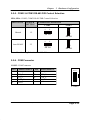
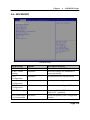
1
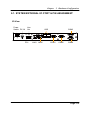
FPC 7719
Industrial Fanless Panel PC
User Manual
FPC7719: Industrial Fanless Touch Panel PC with
Atom D2550 1.86GHz Processor
14628 Central Ave,
Chino, CA 91710
tel:909.597.7588, fax:909.597.1939
© Copyright 2014 Acnodes, Inc.
All rights reserved. Product description and product specifications
are subject to change without notice. For latest product information,
please visit Acnodes’ web site at www.acnodes.com.
COPYRIGHT NOTICE & TRADEMARK
All trademarks and registered trademarks mentioned herein are the property of their
respective owners.
This manual is copyrighted in Dec. 2013. You may not reproduce or transmit in any
form or by any means, electronic, or mechanical, including photocopying and
recording.
DISCLAIMER
This user’s manual is meant to assist you in installing and setting up the system. The
information contained in this document is subject to change without any notice.
CE NOTICE
This is a class A product. In a domestic environment this product may cause radio
interference in which case the user may be required to take adequate measures.
FCC NOTICE
This equipment has been tested and found to comply with the limits for a Class A
digital device, pursuant to part 15 of the FCC Rules. These limits are designed to
provide reasonable protection against harmful interference when the equipment is
operated in a commercial environment. This equipment generates, uses, and can
radiate radio frequency energy and, if not installed and used in accordance with the
instruction manual, may cause harmful interference to radio communications.
Operation of this equipment in a residential area is likely to cause harmful interference
in which case the user will be required to correct the interference at his own expense.
You are cautioned that any change or modifications to the equipment not expressly
approve by the party responsible for compliance could void your authority to operate
such equipment.
CAUTION! Danger of explosion if battery is incorrectly replaced. Replace only with the same or
equivalent type recommended by the manufacturer. Dispose of used batteries according to the
manufacturer’s instructions.
WARNING! Some internal parts of the system may have high electrical voltage. And therefore
we strongly recommend that qualified engineers can open and disassemble the system. The
LCD and touch screen are easily breakable, please handle them with extra care.
Contents
TABLE OF CONTENTS
CHAPTER 1 INTRODUCTION
1-1
1-2
1-3
1-4
About This Manual....................................................................
System Illustration......................................................................
System Specifications.................................................................
Safety Precautions......................................................................
1-2
1-3
1-5
1-7
CHAPTER 2 SYSTEM CONFIGURATION
2-1
2-2
System External I/O Port & Pin Assignment..............................
Mainboard Component Locations & Jumper Settings................
2-2
2-6
CHAPTER 3 SOFTWARE UTILITIES
3-1
3-2
3-3
3-4
3-5
3-6
Introduction................................................................................
Intel® Chipset Software Installation Utility…..……..................
VGA Driver Utility....................................................................
LAN Driver Utility……………………………………………..
Sound Driver Utility……………………………………………
Touchscreen Driver Utility…………………………………….
3-2
3-3
3-4
3-5
3-6
3-7
CHAPTER 4 AMI BIOS SETUP
4-1
4-2
4-3
4-4
4-5
4-6
4-7
4-8
Introduction................................................................................
Entering Setup............................................................................
Main……...................................................................................
Advanced…………………….........................….......................
Chipset……………....................................................................
Boot..………………..................................................................
Security………………………………………………………...
Save & Exit…………………………………………………….
APPENDIX
4-2
4-4
4-7
4-9
4-35
4-41
4-44
4-45
A SYSTEM DIAGRAMS
Exploded Diagram for Whole System of FPC7719...............................
A-2
Contents
APPENDIX
B TECHNICAL SUMMARY
Block Diagram......................................................................................
Interrupt Map.........................................................................................
DMA Channels Map……......................................................................
I/O Map.............................................................................................. ...
Watchdog Timer Configuration…………..…………………………...
Flash BIOS Update…………………………………………………….
B-2
B-3
B-4
B-5
B-8
B-10
CHAPTER
INTRODUCTION
1
This chapter gives you the information for FPC7719. It also outlines the
System specification.
Section includes:
About This Manual
System Specifications
Safety Precautions
Experienced users can skip to chapter 2 on page 2-1
for Quick Start.
Page:1-1
Chapter 1
Introduction
1-1. ABOUT THIS MANUAL
Thank you for purchasing our FPC7719 Atom D2550 processor, 19” fanless & low
power panel PC with DVI,4COM and 2LAN. FPC7719 provides faster processing
speed, greater expandability and can handle more task than before. This manual is
designed to assist you how to install and set up the system. It contains four chapters.
The user can apply this manual for configuration according to the following chapters:
Chapter 1 Introduction
This chapter introduces you to the background of this manual, and the specifications
for this system. The final page of this chapter will indicate how to avoid damaging this
board.
Chapter 2 Hardware Configuration
This chapter outlines the component locations and their functions. In the end of this
chapter, you will learn how to set jumper and how to configure this card to meet your
own needs.
Chapter 3 Software Utilities
This chapter contains helpful information for proper installations of the VGA utility,
LAN utility, and Sound utility.
Chapter 4 BIOS Setup
This chapter indicates you how to set up the BIOS configurations.
Appendix A System Diagrams
This appendix gives you the exploded diagrams and part numbers of the FPC7719.
Appendix B Technical Summary
This appendix gives you the information about the Technical maps, Watchdog-timer
configuration, and Flash BIOS Update.
′
Page: 1-2
Chapter 1
Introduction
1-2. SYSTEM ILLUSTRATION
Front View
471
381
Touch area
396
305.7
Rear View
449
435
276
92
75
240
147.5
100
360
135
96
217
187
96
75
187
100
326
Unit: mm
Page: 1-3
Chapter 1
Introduction
Top View
Bottom View
Side View
Quarter View
18
240
11.2
39.8
79.8
Unit: mm
Page: 1-4
Chapter 1
Introduction
1-3. SYSTEM SPECIFICATION
System
CPU Support
Intel® D2550, 1.86 GHz, 1M Cache, 6.5W
Chipset
OS Support
Memory Support
Watchdog
Drive Bay
Power Supply
Front Bezel
IP65
Mounting Type
Net Weight
Intel® NM10
Microsoft Windows 7 (x86), POSReady 7
1 x DDR3 SO-DIMM socket, 1067 MHz, up to 4 GB
1~255s Watchdog timer
Dimension (W x H x D)
471 x 396 x 79.8 mm
Certificate
CE/FCC
1 x 2.5” SATA HDD
DC-in 9~36V
Aluminum
For front panel only
VESA 75/100
8 .21 kg
I/O Ports
4 x COM ports (COM1,2,3 are RI/5V/12V selectable.):
COM1/4 for RS-232 only
COM2/3 for RS-232/422/485
4 x USB 2.0
1 x DVI-I
2 x LAN, RJ45, Realtek, 10/100/1000 Mbps:
1 x Line-out, Realtek ALC888S high definition:
1 x Mini-PCIe slot
1 x CFast card slot
Serial Port
USB
DVI
LAN
Audio
Expansion slot
′
Page: 1-5
Chapter 1
Introduction
Display
LCD Panel Size
19” TFT
Resolution (Brightness)
1280 x 1024 SXGA 300nit LED backlight
Touchscreen
(ELO) 5W Analog resistive (USB interface)
Environment
Operating Temp.
HDD: 0 ~ 45°C (32 ~ 113°F)
CFast card: 0 ~ 55°C (32 ~ 131°F)
-5 ~ 60°C (23 ~ 140°F)
20 ~ 90%
Storage Temp.
Humidity
′
Page: 1-6
Chapter 1
Introduction
1-4. SAFETY PRECAUTIONS
Follow the messages below to avoid your systems from damage:
1.
Keep your system away from static electricity on all occasions.
2.
Prevent electric shock. Don’t touch any components of this card when the card is
power-on. Always disconnect power when the system is not in use.
3.
Disconnect power when you change any hardware devices. For instance, when
you connect a jumper or install any cards, a surge of power may damage the
electronic components or the whole system.
′
Page: 1-7
CHAPTER
HARDWARE
CONFIGURATION
2
** QUICK START **
Helpful information describes the jumper & connector settings, and
component locations.
Section includes:
Jumper & Connector Quick Reference Table
Component Locations
Configuration and Jumper settings
Connector’s Pin Assignments
Page 2-1
Chapter 2
Hardware Configuration
2-1. SYSTEM EXTERNAL I/O PORT & PIN ASSIGNMENT
I/O View
Power
Switch DC IN
Line
Out
DVI
USB
LAN1 LAN2
′
COM3
COM1
COM2
COM4
Page: 2-2
Chapter 2
Hardware Configuration
2-1-1. DC IN Port
DC IN: DC Power-In Port
PIN
1
2
ASSIGNMENT
GND
GND
PIN
3
4
ASSIGNMENT
VCC24_SB_VIN
VCC24_SB_VIN
4
2
3
1
DC IN
2-1-2. Audio Jack
Line-Out: Audio Line-Out Jack
Connected from Audio1 connector.
Refer to Audio1 pin assignment in section Mainboard
Components Locations & Jumper Settings.
Line-Out
2-1-3. COM Ports
COM1, COM2, COM3, COM4: COM Ports
PIN ASSIGNMENT
PIN ASSIGNMENT
1
DCD_C
6
DSR_C
2
RX_C
7
RTS_C
3
TX_C
8
CTS_C
4
DTR_C
9
RI_SEL
5
GND
Note: COM3 & COM4 ports are connected from
connectors on board. Refer to the section COM
connector.
′
5
9
1
6
COM1/
COM2/
COM3/
COM4
Page: 2-3
Chapter 2
Hardware Configuration
2-1-4. DVI Port
C1 C2
1
9
17
C3 C5 C4
DVI1
DVI: DVI-I Port
PIN
1
2
3
4
5
6
7
8
9
10
11
12
13
14
15
ASSIGNMENT
TMDS_2TMDS_2+
GND
NC
NC
DDC_CLK
DDC_DATA
VSYNC
TMDS_1TMDS_1+
GND
NC
NC
5V
GND
PIN
16
17
18
19
20
21
22
23
24
C1
C2
C3
C4
C5
C6
′
ASSIGNMENT
HPD
TMDS_0TMDS0+
GND
NC
NC
GND
TMDS_CLK+
TMDS_CLKRED
GREEN
BLUE
HSYNC
GND
GND
Page: 2-4
Chapter 2
Hardware Configuration
2-1-5. LAN Port
LAN1, LAN2: RJ45 LAN Ports
PIN
1
2
3
4
ASSIGNMENT
MDI0_DP
MDI0_DN
MDI1_DP
MDI1_DN
PIN
5
6
7
8
Green Yellow
ASSIGNMENT
MDI2_DP
MDI2_DN
MDI3_DP
MDI3_DN
8
1
LAN1/
LAN2
LAN LED Indicator:
Left Side LED
Green Color On
Orange Color On
Off
10/100 LAN Speed Indicator
Giga LAN Speed Indicator
No LAN switch/hub connected.
Right Side LED
Yellow Color Blinking
Off
LAN Message Active
No LAN Message Active
2-1-6. USB Ports
USB Ports: Two USB Double Stack Connectors
PIN
1
2
3
4
ASSIGNMENT
+5V
DN
DP
GND
PIN
5
6
7
8
ASSIGNMENT
+5V
DN
DP
GND
5
8
1
4
USB
′
Page: 2-5
Chapter 2
Hardware Configuration
2-2. MAINBOARD COMPONENT LOCATIONS & JUMPER
SETTINGS
M/B: SB-6310
COM2
COM1
JDVI1
LAN2
JUSB3 JUSB2
2
10
9
1
9
10
1
2
AUDIO1
PWR_IN1
LAN1
JP14 1JP15
6
5
2
1
2
1
JP13
6
5
JP12
JLINE_OUT
JP11
1
COM3
JP8
1
1
2
9
10
6
5
21
4
6 1
1
21
3
3
3
JP17
10 5
2
1
1
JP10
SPK_L_OUT1
SPK_R_OUT1
JP9
JP7
HDD_POWER1
1
1
3
1
3
3
1
SATA1
7
JP16
5
®
Intel
NM10
JTP1
1
Intel ®
N2800/
D2550
2
1
PWR_BTN1
2
1
PWR_LED1
J1
1
7
3
Battery JHDD_LED1
21
SIO
2
1
CPUFAN1
2
8
1
INV1
JP5
RST_BTN1
2
9
SP1
1
JP_PWM1
10
1
1
3
9
1
203
73 71
204
74 72
1
2
1
29 30
1
J2
LVDS1
1
1
5
COM4
16
2
1
6
5
8
2
JP_VDD1
JTAG1
1
OSD_CTRL1
2
1
16 18
15 17
52
51
M_PCIE1
JP1
JP2
JP3
JP4
9
JP_BLEN1
JP_BRCTR1
1 1 1 1
1
JP6
5 10
2
6
DIMM1
JUSB6
5
1
5
1
JUSB7
FPC7719 Connectors, Jumpers and Component locations
′
Page: 2-6
Chapter 2
Hardware Configuration
JCFAST1
S1
S7
PC1
PC17
Component Location
′
Page: 2-7
Chapter 2
Hardware Configuration
2-2-1. Jumpers & Connectors Quick Reference Table
JUMPER/CONNECTOR
COM Ports RI & Voltage Selection
COM2 & COM3 RS-232/422/485
COM2 & COM3 RS-485 DIR Control
Selection
COM Connector
USB Connector
CFAST Voltage Selection
Low Pin Count Connector
SPI Connector
SATA Connector
Mini-PCIe Connector
Clear CMOS Data Selection
CPLD Connector
LCD Panel Resolution Selection
LCD Panel Brightness Control Selection
LCD Panel Backlight Selection
Touch Panel Connector
LED Backlight Connector
OSD Function Connector
LVDS Connector
LVDS Voltage Selection
Pull-In Mode Selection
Run Pin Selection
Power Mode Selection
Power LED Connector
Power Button Connector
Reset Button Connector
HDD Power Connector
HDD LED Connector
Fan Connector
Audio Connector
′
NAME
JP12, JP13, JP8, JP6
JP15, JP17
JP14, JP16
COM3, COM4
JUSB6, JUSB7
JP11
J2
J1
SATA1
M_PCIE1
JP5
JTAG1
JP1, JP2, JP3, JP4
JP_BRCTR1
JP_BLEN1, JP_PWM1
JTP1
INV1
OSD_CTRL1
LVDS1
JP_VDD1
JP7
JP9
JP10
PWR_LED1
PWR_BTN1
RST_BTN1
HDD_POWER1
JHDD_LED1
CPUFAN1
Audio1, SPK_L_OUT1, SPK_R_OUT1
Page: 2-8
Chapter 2
Hardware Configuration
2-2-2. How to Set Jumpers
You can configure your board by setting jumpers. Jumper is consists of two or three
metal pins with a plastic base mounted on the card, and by using a small plastic "cap",
Also known as the jumper cap (with a metal contact inside), you are able to connect
the pins. So you can set-up your hardware configuration by "open" or "close" pins.
The jumper can be combined into sets that called jumper blocks. When the jumpers
are all in the block, you have to put them together to set up the hardware configuration.
The figure below shows how this looks like.
Jumpers & Caps
If a jumper has three pins (for examples, labelled PIN1, PIN2, and PIN3), You can
connect PIN1 & PIN2 to create one setting by shorting. You can either connect PIN2
& PIN3 to create another setting. The same jumper diagrams are applied all through
this manual. The figure below shows what the manual diagrams look and what they
represent.
′
Page: 2-9
Chapter 2
Hardware Configuration
Jumper Diagrams
Jumper Cap
looks like this
2 pin Jumper
looks like this
3 pin Jumper
looks like this
Jumper Block
looks like this
Jumper Settings
2 pin Jumper close(enabled)
Looks like this
1
1
3 pin Jumper
2-3 pin close(enabled)
Looks like this
1
1
Jumper Block
1-2 pin close(enabled)
Looks like this
1
1 2
′
2
Page: 2-10
Chapter 2
Hardware Configuration
2-2-3. COM Ports RI & Voltage Selection
JP12, JP13, JP8, JP6 (Reserved): COM1, 2, 3, 4 Ports RI & Voltage Selection
SELECTION
JUMPER JUMPER ILLUSTRATION
SETTING
COM1
COM2
COM3
COM4
(Reserved)
RI
2
1
1-2
6
5
JP12
12V
2
1
3-4
JP12
5V
5-6
2
1
2
1
6
5
2
1
6
5
2
1
JP13
6
5
2
1
JP8
2
1
6
5
2
1
2
1
6
5
JP6
6
5
JP8
6
5
JP6
JP8
JP13
6
5
JP12
5
JP13
6
5
2
1
6
2
1
6
5
JP6
Note: Manufacturing Default is RI.
′
Page: 2-11
Chapter 2
Hardware Configuration
2-2-4. COM2 & COM3 RS-232/422/485 Selection
JP15, JP17: COM2, COM3 RS-232/422/485 Selection
SELECTION
RS-232
JUMPER
SETTING
All open
JUMPER ILLUSTRATION
COM2
2
1
COM3
1
2
9
10
10
9
JP15
JP17
RS-422
1-2, 3-4, 9-10
2
1
1
2
9
10
10
9
JP15
JP17
RS-485
1-2, 5-6, 7-8
2
1
1
2
9
10
10
9
JP15
JP17
Note: Manufacturing Default is RS-232.
′
Page: 2-12
Chapter 2
Hardware Configuration
2-2-5. COM 2 & COM3 RS-485 DIR Control Selection
JP14, JP16: COM2, COM3 RS-485 DIR Control Selection
SELECTION
JUMPER
SETTING
JUMPER ILLUSTRATION
COM2
1
Manual
3
1-2
3
1
JP14
1
Auto RS-485
COM3
3
2-3
JP16
3
1
JP14
JP16
Note: Manufacturing Default is Auto RS-485.
2-2-6. COM Connector
COM3: COM Connector
PIN
1
2
3
4
5
ASSIGNMENT
DCD_C
RX_C
TX_C
DTR_C
GND
PIN
6
7
8
9
ASSIGNMENT
DSR_C
RTS_C
CTS_C
RI_SEL
10 5
6 1
COM3
′
Page: 2-13
Chapter 2
Hardware Configuration
COM4: COM Connector
PIN
1
2
3
4
5
ASSIGNMENT
DCD_C
RX_C
TX_C
DTR_C
GND
PIN
6
7
8
9
1 6
ASSIGNMENT
DSR_C
RTS_C
CTS_C
RI_SEL
5 10
COM4
2-2-7. USB Connector
JUSB6, JUSB7: USB Connectors
PIN
1
2
3
ASSIGNMENT
+5V
DN
DP
PIN
4
5
ASSIGNMENT
GND
GND
5
1
JUSB6/
JUSB7
2-2-8. CFAST Voltage Selection
JP11 : CFast Voltage Selection
SELECTION JUMPER SETTINGS JUMPER ILLUSTRATION
1
3.3V
3
1-2
JP11
1
5V
3
2-3
JP11
Note: Manufacturing Default is 3.3V.
′
Page: 2-14
Chapter 2
Hardware Configuration
2-2-9. Low Pin Count Connector
2
1
J2: Low Pin Count Connector
PIN
1
2
3
4
5
ASSIGNMENT
CLK_LPCPT
GND
LPC_FRAMEJ
GND
PLTRSTJ_BUF
PIN
6
7
8
9
10
10
9
ASSIGNMENT
LPC_AD0
LPC_AD3
LPC_AD2
VCC3_3
LPC_AD1
J2
ASSIGNMENT
MISO_R
MOSI_R
NC
NC
1
2
7
8
2-2-10. SPI Connector
J1: SPI Connector
PIN
1
2
3
4
ASSIGNMENT
+3.3V
GND
CSJ_R
CLK_R
PIN
5
6
7
8
J1
2-2-11. SATA Connector
SATA1: SATA Connector
1
2
3
4
GND
TX_DP
TX_DN
GND
5
6
7
RX_DN
RX_DP
GND
1
7
SATA1
′
Page: 2-15
Chapter 2
Hardware Configuration
2-2-12. Mini-PCIe Connector
M_PCIE1: Mini-PCIe Connector
PIN
1
2
3
4
5
6
7
8
9
10
11
12
13
14
15
16
17
18
19
20
21
22
23
24
25
26
ASSIGNMENT
WAKEJ
VCC3_3_SB
NC
GND
NC
VCC1_5
M_PCIE_CLKREQJ
SIM_PWR
GND
SIM_DATA
MINI_PCIE_CLK_
DN
SIM_CLK
MINI_PCIE_CLK_
DP
SIM_RESET
GND
SIM_VPP
SIM_SW2
GND
SIM_SW1
NC
GND
PLTRSTJ_BUF
PCIE_RX4_DN
VCC3_3_SB
PCIE_RX4_DP
GND
′
PIN
27
28
29
30
31
32
33
34
35
36
37
38
39
40
41
42
43
44
45
46
47
48
49
50
51
52
ASSIGNMENT
GND
VCC1_5
GND
SMB_CLK
PCIE_TXN4
SMB_DATA
PCIE_TXP4
GND
GND
USB5_DN
GND
2
1
16 18
15 17
52
51
M_PCIE1
USB5_DP
VCC3_3_SB
GND
VCC3_3_SB
NC
GND
LED_WLANJ
NC
NC
NC
VCC1_5
NC
GND
NC
VCC3_3_SB
Page: 2-16
Chapter 2
Hardware Configuration
2-2-13. Clear CMOS Data Selection
JP5 : Clear CMOS Data Selection
SELECTION JUMPER SETTINGS JUMPER ILLUSTRATION
1
Normal
Open
JP5
1
Clear CMOS*
Close
JP5
Note: Manufacturing Default is Normal.
*To clear CMOS data, user must power-off the computer and set the jumper to “Clear
CMOS” as illustrated above. After five to six seconds, set the jumper back to “Normal”
and power-on the computer.
2-2-14. CPLD Connector
JTAG1: CPLD Connector
PIN
1
2
3
4
ASSIGNMENT
+3.3V
TDO
TDI
NC
PIN
5
6
7
8
′
ASSIGNMENT
NC
TMS
GND
TCK
8
1
JTAG1
Page: 2-17
Chapter 2
Hardware Configuration
2-2-15. LCD Panel Resolution Selection
JP1, JP2 JP3, JP4: LCD Panel Resolution Selection
SELECTION
1024 x 768
1CH/24bit
1280 x 1024
2CH/24bit
JUMPER
SETTING
JP1: 2-3
JP2: 2-3
JP3: 1-2
JP4: 2-3
JP1: 2-3
JP2: 1-2
JP3: 1-2
JP4: 2-3
JUMPER ILLUSTRATION
1
1
1
1
3
3
3
3
JP1
JP2
JP3
JP4
1
1
1
1
3
3
3
3
JP1
JP2
JP3
JP4
Note: Manufacturing Default is RI.
2-2-16. LCD Panel Brightness Control Selection
JP_BRCTR1: LCD Panel Brightness Control Selection
SELECTION JUMPER SETTINGS JUMPER ILLUSTRATION
3
LED
1
1-2
JP_BRCTR1
3
CCFL
1
2-3
JP_BRCTR1
Note: Manufacturing Default is LED.
Page: 2-18
Chapter 2
Hardware Configuration
2-2-17. LCD Panel Backlight Selection
JP_BLEN1: LCD Panel Backlight Voltage Control Selection
SELECTION JUMPER SETTINGS JUMPER ILLUSTRATION
3
3.3V
1
1-2
JP_BLEN1
3
5V
1
2-3
JP_BLEN1
Note: Manufacturing Default is 3.3V.
JP_PWM1: Backlight Control Type Selection
SELECTION JUMPER SETTINGS JUMPER ILLUSTRATION
1
Hardware
3
1-2
JP_PWM1
1
Software
3
2-3
JP_PWM1
Note: Manufacturing Default is Software.
′
Page: 2-19
Chapter 2
Hardware Configuration
2-2-18. Touch Panel Connector
JTP1: Touch Panel Connector
PIN
1
ASSIGNMENT
LR
3
PROBE
PIN
4
5
ASSIGNMENT
UR
1
JTP1
2-2-19. LED Backlight Connector
INV1: LED Backlight Connector
PIN
1
2
3
4
5
ASSIGNMENT
+12V
+12V
+12V
NC
GND
PIN
6
7
8
9
ASSIGNMENT
GND
GND
BLEN
BRCTR
9
1
INV1
2-2-20. OSD Function Connector
OSD_CTRL1: OSD Function Connector
PIN
1
2
3
4
5
ASSIGNMENT
BLPU
BLPD
GND
VOLPU
VOLPD
PIN
6
7
8
9
′
ASSIGNMENT
BKLT_PWRBTNJ
OSD_HOME
VCC5
VCC3_3
9
1
OSD_CTRL
Page: 2-20
Chapter 2
Hardware Configuration
2-2-21. LVDS Connector
LVDS1: LVDS Connector
PIN
1
2
3
4
5
6
7
8
9
10
11
12
13
14
15
ASSIGNMENT
VCC
GND
CLKB_DN
CLKB_DP
GND
B2_DN
B2_DP
GND
B1_DN
B1_DP
B3_DP
B3_DN
B0_DP
B0_DN
GND
PIN
16
17
18
19
20
21
22
23
24
25
26
27
28
29
30
ASSIGNMENT
CLKA_DP
CLKA_DN
GND
A2_DP
A2_DN
GND
A1_DP
A1_DN
GND
A0_DP
A0_DN
A3_DP
A3_DN
VCC
VCC
29 30
1
2
LVDS1
2-2-22. LVDS Voltage Selection
JP_VDD1: Power Mode Selection
SELECTION JUMPER SETTINGS JUMPER ILLUSTRATION
3.3V
1-3, 2-4
1
2
5
6
JP_VDD1
5V
3-5, 4-6
1
2
5
6
JP_VDD1
Note: Manufacturing Default is 3.3V.
′
Page: 2-21
Chapter 2
Hardware Configuration
2-2-23. Pull-In Mode Selection
JP7: Pull-In Mode Selection
SELECTION JUMPER SETTINGS JUMPER ILLUSTRATION
1
On
1-2
3
JP7
1
Off
2-3
3
JP7
Note: Manufacturing Default is Off.
2-2-24. Run Pin Selection
JP9: Run Pin Selection
SELECTION JUMPER SETTINGS JUMPER ILLUSTRATION
1
On
1-2
3
JP9
1
Off
2-3
3
JP9
Note: Manufacturing Default is On.
′
Page: 2-22
Chapter 2
Hardware Configuration
2-2-25. Power Mode Selection
JP10: Power Mode Selection
SELECTION JUMPER SETTINGS JUMPER ILLUSTRATION
3
AT
1-2
1
JP10
3
ATX
2-3
1
JP10
Note: Manufacturing Default is ATX.
2-2-26. Power LED Connector
PWR_LED1: Power LED Connector
PIN
1
2
2
1
ASSIGNMENT
+5V
GND
PWR_LED1
2-2-27. Power Button Connector
PWR_BTN1: Power Button Connector
PIN
1
2
2
1
ASSIGNMENT
PWRBTNJ
GND
PWR_BTN1
′
Page: 2-23
Chapter 2
Hardware Configuration
2-2-28. Reset Button Connector
RST_BTN1: Speaker Connector
PIN
1
2
2
1
ASSIGNMENT
RST_IN
GND
RST_BTN1
2-2-29. HDD Power Connector
HDD_POWER1: HDD Power Connector
PIN
1
2
ASSIGNMENT
+5V
GND
PIN
3
4
ASSIGNMENT
GND
+12V
4
1
HDD_POWER1
2-2-30. HDD LED Connector
JHDD_LED1: Power LED Connector
PIN
1
2
ASSIGNMENT
+3.3V
GND
2 1
JHDD_LED1
2-2-31. Fan Connector
CPUFAN1: Fan Connector
PIN
1
2
3
3
ASSIGNMENT
GND
OUT
+12V
1
CPUFAN1
′
Page: 2-24
Chapter 2
Hardware Configuration
2-2-32. Audio Connector
AUDIO1: Audio Connector
PIN
1
2
3
4
5
ASSIGNMENT
MIC_IN
M1C_VDD
GND
GND
LINE_L
PIN
6
7
8
9
10
ASSIGNMENT
LINE-R
GND
GND
SPK_L
SPK_R
9
10
1
2
AUDIO1
SPK_L_OUT1: Speaker Connector
PIN
1
2
ASSIGNMENT
SPKL_P
SPKL_M
21
SPK_L_OUT1
SPK_R_OUT1: Speaker Connector
PIN
1
2
ASSIGNMENT
SPKR_P
SPKR_M
21
SPK_R_OUT1
′
Page: 2-25
SOFTWARE
UTILITIES
CHAPTER
3
This chapter comprises the detailed information of VGA driver, LAN
driver, and Sound driver.
Section includes:
Introduction
Intel® Chipset Software Installation Utility
VGA Driver Utility
LAN Driver Utility
Sound Driver Utility
Touchscreen Driver Utility
Page: 3-1
Chapter 3
Software Utilities
3-1. INTRODUCTION
Enclosed with our FPC7719 package, you will find a CD ROM disk containing all
types of drivers we have. As a FPC7719 user, you will only need some of files
contained in the CD ROM disk, please take note of the following chart:
FILE NAME
(Assume that CD ROM drive is D:)
D:\Driver\Plaform\[OS]\MainChip
PURPOSE
Intel® Chipset Device Software installs
Windows INF files to the target system.
D:\Driver\Plaform\[OS]\VGA
Intel® HD Graphics installer for Embedded
Media and Graphics Driver installation
D:\Driver\Plaform\[OS]\LAN
Realtek RTL8111F for LAN driver
installation
D:\Driver\Plaform\[OS]\SOUND
Realtek ALC888S High Definition Audio
for sound driver installation
D:\Driver\Device\Touch Screen
eGalax Touch Controller for Windows
installation
D:\Driver\Flash BIOS
AMI BIOS update utility
Note: Be sure to install the Utility right after the OS is fully installed.
′
Page:3-2
Chapter 3
Software Utilities
3-2. INTEL® CHIPSET SOFTWARE INSTALLATION UTILITY
3-2-1. Introduction
The Intel® Chipset Device Software installs Windows *.INF files to the target system.
These files outline to the operating system how to configure the Intel® chipset
components in order to ensure that the following features function properly:
PCIe Support
SATA Storage Support
USB Support
Identification of Intel® Chipset Components in the Device Manager
3-2-2. Installation of Utility for Windows 7/POSReady 7
The Utility Pack is made only for Windows 7/POSReady 7. It should be installed right
after the OS installation; kindly follow the following steps:
1.
2.
3.
4.
5.
Place insert the Utility Disk into the CD ROM drive.
Under Windows system, go to the directory where Utility Disc is located.
e.g.: D:\Driver\Platform\(OS)\Utility\infinst_autol.exe
Click infinst_autol.exe file for utility installation.
Follow the instructions on the screen to complete the installation.
Once installation is completed, shut down the system and restart in order for the
changes to take effect.
′
Page:3-3
Chapter 3
Software Utilities
3-3. VGA DRIVER UTILITY
The VGA interface is embedded with our FPC7719 system to support CRT
display. The following illustration briefly shows you the content of VGA driver.
1. Win 7 Series
2. POSReady 7
3-3-1. Installation of VGA Driver for Windows 7/POSReady 7
1.
2.
3.
4.
Start the computer.
Insert the Utility Disk into the CD ROM drive.
Open the VGA folder for your system to choose an appropriate folder, and
double-click "*.exe" file to install.
e.g. D:\Driver\Platform\(OS)\Graphics\Your system\ ***.exe
(If D is not your CD-ROM drive, substitute D with the correct drive letter.)
Follow the Wizard's on-screen instructions to complete the installation.
′
Page:3-4
Chapter 3
Software Utilities
3-4. LAN DRIVER UTILITY
3-4-1. Introduction
The FPC7719 is enhanced with LAN function that can support various network
adapters. The content of the LAN driver is found as follows:
1. Win 7 Series
2. POSReady 7
For more details on Installation procedure, please refer to Readme.txt file
found on LAN DRIVER UTILITY.
′
Page:3-5
Chapter 3
Software Utilities
3-5. SOUND DRIVER UTILITY
3-5-1. Introduction
The Audio chip enhanced in this system is fully compatible with Windows 7. Below,
you will find the content of the Sound driver:
1. Win 7 Series
2. POSReady 7
3-5-2. Installation Procedure for Windows 7/POSReady 7
1.
2.
3.
Open the “Sound” folder. For your system to choose an appropriate folder, and
Run the setup.exe program to start the installation.
e.g.: D:\Driver\Platform\(OS)\ SOUND\Your system\setup.exe
(If D is not your CD-ROM drive, substitute D with the correct drive letter.)
Click on [Next] to continue the procedure. If the Windows popup "Windows
can't verify the publisher of this driver software" message, press "Install this
driver software anyway" to continue the installation.
Finally, select to restart the system and press [Finish] to complete the installation.
′
Page:3-6
Chapter 3
Software Utilities
3-6. TOUCHSCREEN DRIVER UTILITY
The touch screen driver utility can only be installed on Windows 7, and it should be
installed right after the OS installation.
1. Win 7 Series
2. POSReady 7
3-6-1. Installation of Touchscreen Driver for Windows 7/POSReady 7
To install the touchscreen driver, follow the steps below:
1.
2.
3.
4.
Open the “Device/Touchscreen” folder where the touchscreen driver is located.
Click Setup.exe file for driver installation.
Follow the on-screen instructions to complete the installation.
Once installation is completed, shut down the system and restart for the changes
to take effect.
′
Page:3-7
CHAPTER
BIOS SETUP
4
This chapter shows how to set up the AMI BIOS.
Section includes:
Introduction
Entering Setup
Main
Advanced
Chipset
Boot
Security
Save & Exit
Page: 4-1
Chapter 4
AMI BIOS Setup
4-1. INTRODUCTION
The system FPC7719 uses an AMI (American Megatrends Incorporated) Aptio
BIOS that is stored in the Serial Peripheral Interface Flash Memory (4MB SPI Flash)
and can be updated. The SPI Flash contains the BIOS (Basic Input Output
System) setup menu, Power-on Self-test (POST), the PCI auto-configuration utility,
LAN EEPROM information, and Plug and Play support.
Aptio is AMI’s BIOS firmware based on the UEFI (Unified Extensible Firmware
Interface) specifications and the Intel Platform Innovation Framework for EFI. The
UEFI specification defines an interface between an operating system and platform
firmware. The interface consists of data tables that contain platform-related
information, boot service calls, and runtime service calls that are available to the
operating system and its loader. These provide standard environment for booting an
operating system and running pre-boot applications.
Following illustration shows Extensible Firmware Interface’s position in the software
stack.
′
Page: 4-2
Chapter 4
AMI BIOS Setup
EFI BIOS provides an user interface allow users the ability to modify hardware
configuration, e.g. change system date and time, enable or disable a system component,
decide bootable device priorities, setup personal password, etc., which is convenient
for modifications and customization of the computer system and allows technicians
another method for finding solutions if hardware has any problems.
The BIOS setup menu can be used to view and change the BIOS settings for the
computer. The BIOS setup menu is accessible by pressing the <Del> or <F2> key on
keyboard during the POST stage, right before the operating system is loading. All the
settings are described in chapter to be followed.
′
Page: 4-3
Chapter 4
AMI BIOS Setup
4-2. ENTERING SETUP
When the system is powered on, the BIOS will enter the Power-on Self-test (POST)
routines and the following message will appear on the lower screen:
Version: 2.15.1226. Copyright (C) 2012 American Magatrends, Inc.
BIOS Date: 02/23/2013 14:11:05 Ver: 63100P01
Press <DEL> or <F2> to enter setup.
First POST screen with AMI logo
For as long as this message is present on the screen before the operating system boot
begins, you may press the <Del> or <F2> key (the one that shares the decimal point
at the bottom of the number keypad) to access the setup menu. In a moment, the
main menu of the Aptio Setup Utility will appear on the screen:
′
Page: 4-4
Chapter 4
AMI BIOS Setup
BIOS setup program initial screen
The BIOS setup menu interface and help messages are shown in US English. You may
move the cursor by up/down keys to highlight the individual menu items. As you
highlight each item, a brief description of the highlighted selection will appear at the
bottom of the screen.
′
Page: 4-5
Chapter 4
AMI BIOS Setup
4-2-1. BIOS Setup Menu Keys
The following table provides list of keys available for BIOS setup menu.
BIOS Setup menu key
<←> and <→>
<↑> and <↓>
<Enter>
<F2>
<F3>
<F4>
<Esc>
Description
Selects a different menu screen (moves the selection left
or right).
Selects an item (moves the selection up or down).
Executes command or selects the sub-menu.
Load the previous configuration values.
Load the default configuration values.
Save the current values and exits the BIOS setup menu.
Leaves the sub-menu.
Triggers confirmation to exit BIOS setup menu.
4-2-2. BIOS Messages
This section describes error messages generated by the board’s BIOS. These messages
would be displayed on the monitor when certain recoverable error/event occurs during
POST stage. The table bellow gives an explanation of the BIOS messages.
BIOS Setup menu key
A first boot or NVRAM
reset condition has been
detected.
The CMOS defaults
were loaded.
The CMOS battery is
bad or was recently
replaced.
Explanation
BIOS has been updated or the battery was replaced.
Default values have been loaded after the BIOS was
updated or the battery was replaced.
The battery may be losing power, replace the battery soon.
Also, this message is displayed once the new battery was
placed.
′
Page: 4-6
Chapter 4
AMI BIOS Setup
4-3. MAIN
Main screen
BIOS Setting
BIOS Vendor
Core Version
Compliancy
Project Version
Options
No changeable options
No changeable options
No changeable options
No changeable options
Build Date and
Time
Intel RC Version
No changeable options
System Date
System Time
Access Level
Month, day, year
Hour, minute, second
No changeable options
Sub-menu
′
Description/Purpose
Displays the BIOS vendor.
Displays the current BIOS core version.
Displays the current UEFI version.
Displays the version of the BIOS and
its architecture compatibility currently
installed on the platform.
Displays the date of current BIOS
version.
Enters sub-menu with information
regarding used components versions.
Specifies the current date.
Specifies the current time.
Displays security levels currently in use.
Page: 4-7
Chapter 4
AMI BIOS Setup
4-3-1. Main – Intel RC Version
Intel RC Version screen
BIOS Setting
Intel Cedarview
Options
No changeable options
Intel MRC
No changeable options
Intel NM10
No changeable options
Intel P-UNIT
Intel iGFX
VBIOS
Intel ACPI
No changeable options
No changeable options
No changeable options
′
Description/Purpose
Displays code version for Intel
D/N2x00 processor.
Displays code version of Intel Memory
Reference Code (MRC), e.g. “1.12”.
Displays code version for Intel NM10
chipset.
Displays code version for power unit.
Displays current version of Intel Video
BIOS (VBIOS), e.g. “1089”.
Displays code version for Advanced
Configuration and Power Interface
(ACPI).
Page: 4-8
Chapter 4
AMI BIOS Setup
4-4. ADVANCED
Advanced screen
BIOS Setting
ACPI Settings
S5 RTC Wake
Settings
CPU
Configuration
IDE
Configuration
USB
Configuration
SMART Settings
Options
Sub-menu
Sub-menu
Sub-menu
Description/Purpose
Enters menu to set ACPI option.
Accesses settings for scheduled S5
power on feature.
All processor basic options menu.
Sub-menu
SATA device configuration section.
Sub-menu
Enters menu to configure USB options.
Sub-menu
Section to SATA HDD/SSD
S.M.A.R.T. capability.
Serial and parallel ports configuration
section.
NCT6106D Super Sub-menu
IO Configuration
′
Page: 4-9
Chapter 4
BIOS Setting
NCT6106D HW
Monitor
WatchDog
Configuration
Network Stack
Options
Sub-menu
CMOS
PPM
Configuration
Sub-menu
Sub-menu
Sub-menu
Sub-menu
′
AMI BIOS Setup
Description/Purpose
Options for NCT6106D hardware
monitor chip.
Section to configure Watchdog timer.
Enters menu to enable network during
DXE stage and UEFI shell
environment.
Options for CMOS battery.
Processor advanced power options
menu.
Page: 4-10
Chapter 4
AMI BIOS Setup
4-4-1. Advanced – APCI Settings
APCI Settings screen
BIOS Setting
Enable ACPI
Auto
Configuration
Enable
Hibernation
Options
-Disabled
-Enabled
ACPI Sleep State
-Suspend Disabled
-S1 only
-S3 only
-Both S1 and S3
-Disabled
-Enabled
′
Description/Purpose
Allows deciding whether ACPI
settings are configured by operating
system or manually (option disabled).
Enables ability to enter S4 state (to be
able to hibernate in Windows
operating system).
Specifies the ACPI sleep state.
Disabled option disables ACPI sleep
feature.
S1 is less common state in which the
CPU is stopped.
S3 allows the platform to enter Sleep
mode (also known as Standby or
Suspend to RAM).
Page: 4-11
Chapter 4
BIOS Setting
Lock Legacy
Resources
Options
-Disabled
-Enabled
S3 Video Repost
-Disabled
-Enabled
AMI BIOS Setup
Description/Purpose
Prevents the operating system from
changing resources to serial or parallel
controller.
If enabled re-initialises the VBIOS
after waking up from an S3 sleep.
Note: It is necessary to modify system registry in order enable wake up from S3
system power state via USB devices in Windows XP.
Simply add DWORD entry named “USBBIOSx” with value 0 to location:
HKEY_LOCAL_MACHINE\SYSTEM\CurrentControlSet\Services\usb\
Fore more details, refer to Microsoft Support article KB 841858 at
http://support.microsoft.com/kb/841858.
′
Page: 4-12
Chapter 4
AMI BIOS Setup
4-4-2. Advanced – S5 RTC Wake Settings [disabled]
S5 RTC wake setting screen
BIOS Setting
Options
Wake system with -Disabled
Fixed Time
-Enabled
Wake system with -Disabled
Dynamic Time
-Enabled
′
Description/Purpose
Allows enabling scheduled S5 to
S0 transition set to specific period
of time (option enabled).
Please note that only one of these
two options can be enabled at the
same moment.
Allows enabling scheduled S5 to
S0 transition set to variable period
of time (option enabled).
Page: 4-13
Chapter 4
AMI BIOS Setup
4-4-3. Advanced – S5 RTC Wake Settings [enabled]
S5 RTC wake setting screen
BIOS Setting
Options
Wake system with -Disabled
Fixed Time
-Enabled
Wake up hour
Wake up minute
Wake up second
Multiple options ranging
from 0 to 23
Multiple options ranging
from 0 to 59
Multiple options ranging
from 0 to 59
′
Description/Purpose
Allows enabling scheduled S5 to
S0 transition set to specific period
of time (option enabled).
Please note that only one of these
two options can be enabled at the
same moment.
Sets an hour for schedule power on
event.
Sets a minute for schedule power
on event.
Sets a second for schedule power
on event.
Page: 4-14
Chapter 4
BIOS Setting
Options
Wake system with -Disabled
Dynamic Time
-Enabled
Wake up minute
increase
Multiple options ranging
from 1 to 5
′
AMI BIOS Setup
Description/Purpose
Allows enabling scheduled S5 to
S0 transition set to variable period
of time (option enabled).
Sets a period of time (in minutes)
after which the board wakes up
from S5 state.
Page: 4-15
Chapter 4
AMI BIOS Setup
4-4-4. Advanced - CPU Configuration
CPU Configuration screen
BIOS Setting
Processor Type
Options
No changeable options
Processor
Stepping
EMT64
No changeable options
Processor Speed
No changeable options
No changeable options
System Bus Speed No changeable options
Ratio Status
No changeable options
Actual Ration
No changeable options
′
Description/Purpose
Displays the current processor model
number and frequency.
Displays the D/N2x000 processor
stepping.
Reports if processor supports Intel
x86-64 (amd64) implementation.
Displays the current processor
frequency.
Displays the bus frequency.
Displays the processor model bus/core
ratio.
Displays the processor current bus/core
ratio.
Page: 4-16
Chapter 4
AMI BIOS Setup
BIOS Setting
Processor
Stepping
Microcode
Revision
L1 Cache RAM
L2 Cache RAM
Processor Cores
Options
No changeable options
Description/Purpose
Displays processor’s ID stepping.
No changeable options
Hyper-Threading
No changeable options
Hyper-threading
-Disabled
-Enabled
-Disabled
-Enabled
-Disabled
-Enabled
Displays processor's microcode update
revision.
Displays amount of Level 1 cache.
Displays amount of Level 2 cache.
Displays information about number of
physical cores in processor.
Reports if Intel Hyper-Threading
Technology is supported by processor.
When disabled, only one thread per
active core will operate.
Execute Disable
Bit
Limit CPUID
Maximum
No changeable options
No changeable options
No changeable options
′
Enables the NX bit (No eXecute)
security feature.
Enables for legacy operating systems to
boot processors with extended CPUID
(CPU Identification) functions.
Page: 4-17
Chapter 4
AMI BIOS Setup
4-4-5. Advanced – IDE Configuration [enabled]
IDE configuration screen
BIOS Setting
SATA Port
CFast Slot
SATA
Controller(s)
Configure SATA
as
Port Speed Limit
Options
No changeable
options
No changeable
options
-Disabled
-Enabled
-IDE
-AHCI
-No Limit
-Gen1
-Gen2
′
Description/Purpose
Displays device ID plugged in SATA port
(if any).
Displays device ID plugged in CFast slot (if
any).
Enables SATA controller.
Configures SATA devices as IDE or AHCI.
It is not advised to change this option once
the operating system is installed.
Configures SATA (only when set as AHCI)
interface as following:
No Limit selects no speed limitation.
Gen1 mode sets the device to 1.5 Gbit/s
Page: 4-18
Chapter 4
BIOS Setting
Options
CFast Slot Speed
Limit
-No Limit
-Gen1
-Gen2
SATA Port
-Disabled
-Enabled
-Disabled
-Enabled
-Disabled
-Enabled
-Disabled
-Enabled
SATA Port Hot
Plug
CFast Slot
CFast Slot Hot
Plug
′
AMI BIOS Setup
Description/Purpose
speed.
Gen2 mode sets the device to 3 Gbit/s
speed (in case it is compatible).
Configures CFast (only when set as AHCI)
interface as following:
No Limit selects no speed limitation.
Gen1 mode sets the device to 1.5 Gbit/s
speed.
Gen2 mode sets the device to 3 Gbit/s
speed (in case it is compatible).
Allows controlling specific SATA port.
Enables Hot Plug feature on SATA port
(if supported by the device).
Allows controlling specific CFast Slot.
Enables Hot Plug feature on CFast slot (if
supported by the device).
Page: 4-19
Chapter 4
AMI BIOS Setup
4-4-6. Advanced – IDE Configuration [disabled]
IDE configuration screen
BIOS Setting
SATA Port0
Options
No changeable options
SATA
Controller(s)
-Disabled
-Enabled
′
Description/Purpose
Displays device ID plugged in SATA
port (if any).
Disables SATA controller.
Page: 4-20
Chapter 4
AMI BIOS Setup
4-4-7. Advanced – USB Configuration
USB Configuration screen
BIOS Setting
USB Devices
Options
No changeable options
Legacy USB
Support
-Disabled
-Enabled
-Auto
-Disabled
-Enabled
EHCI Hand-off
USB transfer
time-out
-1 sec
-5 sec
-10 sec
-20 sec
′
Description/Purpose
Reports number and type of connected
USB devices (if any).
Enables support for USB in legacy
operating systems (e.g. MS-DOS,
Windows NT).
When enabled it allows BIOS support
control of the EHCI controller and the
OS hand-off synchronization capability.
Specifies time-out value for Control,
Bulk and Interrupt transfers.
Page: 4-21
Chapter 4
BIOS Setting
Options
Device reset time- -10 sec
out
-20 sec
-30 sec
-40 sec
Device power-up -Auto
delay
-Manual
Mass Storage
Devices:
[drive(s)]
-Auto
-Floppy
-Forced FDD
-Hard Disk
-CD-ROM
′
AMI BIOS Setup
Description/Purpose
Specifies the value for device reset
timeout.
Specifies maximum time it would take
for USB device to report itself to the
controller.
If set to auto, it would use default
values (100 ms for root port) and value
read from hub descriptor in case of hub
port.
Appears only when USB flash drive is
plugged in. Allows selecting which
emulation to use on available drive(s).
Please note that the sector size of your
USB drive should be emulated device
native sector size.
Page: 4-22
Chapter 4
AMI BIOS Setup
4-4-8. Advanced – SMART Settings
SMART Settings screen
BIOS Setting
Options
SMART Self Test -Disabled
-Enabled
′
Description/Purpose
Enables S.M.A.R.T. (SelfMonitoring, Analysis and Reporting
Technology) feature to be found on
most modern HDD/SSD.
Page: 4-23
Chapter 4
AMI BIOS Setup
4-4-9. Advanced – NCT6106D Super IO Configuration
NCT6106D Super IO Configuration screen
BIOS Setting
NCT6106D Super
IO Chip
Serial Port 1
Configuration
Serial Port 2
Configuration
Serial Port 3
Configuration
Serial Port 4
Configuration
Options
No changeable options
Sub-menu
Description/Purpose
Shows Super IO manufacturer and
model.
Enters menu to configure serial port 1.
Sub-menu
Enters menu to configure serial port 2.
Sub-menu
Enters menu to configure serial port 3.
Sub-menu
Enters menu to configure serial port 4.
′
Page: 4-24
Chapter 4
AMI BIOS Setup
4-4-9-1. NCT6106D Super IO Configuration – Serial Port 1 Configuration
Serial Port 1 Configuration screen
BIOS Setting
Serial Port
Device Settings
Change Settings
Options
-Disabled
-Enabled
No changeable options
-Auto
-IO=3F8h; IRQ=4;
-IO=3F8h; IRQ=3,4,5,6,7,10,11,12;
-IO=2F8h; IRQ=3,4,5,6,7,10,11,12;
-IO=3E8h; IRQ=3,4,5,6,7,10,11,12;
-IO=2E8h; IRQ=3,4,5,6,7,10,11,12;
′
Description/Purpose
Configures the serial port
1.
Shows current settings
applied to the serial port.
Specifies the base I/O
address and interrupt
request for the serial port
1 if enabled.
Page: 4-25
Chapter 4
AMI BIOS Setup
4-4-9-2. NCT6106D Super IO Configuration – Serial Port 2 Configuration
Serial Port 2 Configuration screen
BIOS Setting
Serial Port
Device Settings
Change Settings
Options
-Disabled
-Enabled
No changeable options
-Auto
-IO=3F8h; IRQ=4;
-IO=3F8h; IRQ=3,4,5,6,7,10,11,12;
-IO=2F8h; IRQ=3,4,5,6,7,10,11,12;
-IO=3E8h; IRQ=3,4,5,6,7,10,11,12;
-IO=2E8h; IRQ=3,4,5,6,7,10,11,12;
′
Description/Purpose
Configures the serial port
2.
Shows current settings
applied to the serial port.
Specifies the base I/O
address and interrupt
request for the serial port
2 if enabled.
Page: 4-26
Chapter 4
AMI BIOS Setup
4-4-9-3. NCT6106D Super IO Configuration – Serial Port 3 Configuration
Serial Port 3 Configuration screen
BIOS Setting
Serial Port
Device Settings
Change Settings
Options
-Disabled
-Enabled
No changeable options
-Auto
-IO=3F8h; IRQ=4;
-IO=3F8h; IRQ=3,4,5,6,7,10,11,12;
-IO=2F8h; IRQ=3,4,5,6,7,10,11,12;
-IO=3E8h; IRQ=3,4,5,6,7,10,11,12;
-IO=2E8h; IRQ=3,4,5,6,7,10,11,12;
′
Description/Purpose
Configures the serial port
3.
Shows current settings
applied to the serial port.
Specifies the base I/O
address and interrupt
request for the serial port
3 if enabled.
Page: 4-27
Chapter 4
AMI BIOS Setup
4-4-9-4. NCT6106D Super IO Configuration –Serial Port 4 Configuration
Parallel Port Configuration screen
BIOS Setting
Serial Port
Device Settings
Change Settings
Options
-Disabled
-Enabled
No changeable options
-Auto
-IO=3F8h; IRQ=4;
-IO=3F8h; IRQ=3,4,5,6,7,10,11,12;
-IO=2F8h; IRQ=3,4,5,6,7,10,11,12;
-IO=3E8h; IRQ=3,4,5,6,7,10,11,12;
-IO=2E8h; IRQ=3,4,5,6,7,10,11,12;
′
Description/Purpose
Configures the serial port
4.
Shows current settings
applied to the serial port.
Specifies the base I/O
address and interrupt
request for the serial port
4 if enabled.
Page: 4-28
Chapter 4
AMI BIOS Setup
4-4-10. Advanced – NCT6106D HW Monitor
NCT6106D HW Monitor screen
BIOS Setting
Options
CPU Temperature No changeable options
System
Temperature
CPU Fan Speed
No changeable options
Vcore
No changeable options
+12V
+5V
+1.5V
Vsb3
No changeable options
No changeable options
No changeable options
No changeable options
Vbat
No changeable options
No changeable options
′
Description/Purpose
Shows processor temperature in
degree Celsius.
Monitors system temperature in
degree Celsius.
Monitors processor fan speed if
connected (otherwise shows N/A).
Shows actual voltage of processor
core in volt.
Monitors 12V section (in volt).
Monitors 5V section (in volt).
Monitors 1.5V section (in volt).
Monitors 3.3V standby section (in
volt).
Monitors battery voltage (in volt).
Page: 4-29
Chapter 4
AMI BIOS Setup
4-4-11. Advanced – Watchdog Configuration
Watchdog Configuration screen
BIOS Setting
Watchdog Timer
WatchDog
TimeOut Value
Options
-Second
-Minute
Multiple options ranging
from 0 to 255
′
Description/Purpose
Selects time unit for watchdog timer
feature.
Sets the desired value (in seconds) for
watchdog timeout. Setting value ‘0’
means the watchdog is disabled.
Page: 4-30
Chapter 4
AMI BIOS Setup
4-4-12. Advanced – Network Stack
Network Stack screen
BIOS Setting
Network stack
Options
-Disabled
-Enabled
′
Description/Purpose
Allows for enabling network capability
in DXE stage and UEFI shell.
Page: 4-31
Chapter 4
AMI BIOS Setup
4-4-13. Advanced –CMOS
CMOS screen
BIOS Setting
Bad battery
detected
Options
No changeable options
First boot
detected
Defaults loaded
No changeable options
Bad checksum
detected
No changeable options
No changeable options
′
Description/Purpose
Informs about low voltage on CMOS
backup battery. Please replace the
battery.
Shows that this is first boot after
updating BIOS.
Confirms that loaded default values
has been selected and loaded.
Informs about CMOS memory bad
checksum.
Page: 4-32
Chapter 4
AMI BIOS Setup
4-4-14. Advanced –PPM Configuration
PPM Configuration screen
BIOS Setting
EIST
CPU C state
Report
Options
-Disabled
-Enabled
-Disabled
-Enabled
Enhanced C state
-Disabled
-Enabled
CPU Hard C4E
-Disabled
-Enabled
CPU C6 State
-Disabled
-Enabled
′
Description/Purpose
Enables Intel SpeedStep feature for
dynamic scaling processor frequency.
Enables C states mode as a measure to
save power. In those states, the clock
signal and power is cut from idle units.
Enables enhanced C states, which
allows cutting clock signal and reducing
CPU voltage both at the same time.
Enables enhanced deeper sleep in
which reduces CPU voltage even more
and turns off the cache.
Enabled deep power down C state.
Page: 4-33
Chapter 4
BIOS Setting
C4 Exit Timing
Options
-Default
-Fast
-Slow
C-state
POPDOWN
-Disabled
-Enabled
C-state POPUP
-Disabled
-Enabled
′
AMI BIOS Setup
Description/Purpose
Controls a programmable time for the
CPU voltage to stabilize when exiting
from C4 state. In case of perceptible
audio noise caused by periodically
exiting the C4 state option slow might
eliminate the noise.
When disabled, the CPU will no try to
promote its sleep state from C2 down
to C3/C4.; these last two items are part
of PPM (Processor Power
Management).
Enables popup mode in which CPU
goes from C3 or C4 state into C2
(when disabled it changes straight to
C0).
Page: 4-34
Chapter 4
AMI BIOS Setup
4-5. Chipset
Chipset screen
BIOS Setting
Host Bridge
Options
Sub-menu
South Bridge
Sub-menu
′
Description/Purpose
Enters menu to configure integrated
graphics & memory related items.
Enters menu to configure audio, USB
and power lost items.
Page: 4-35
Chapter 4
AMI BIOS Setup
4-5-1. Chipset – Host Bridge
Host bridge screen
BIOS Setting
Memory
Frequency and
Timing
Intel IGD
Configuration
Memory
Frequency
Options
Sub-menu
Description/Purpose
Enters menu to deal with memory
setting.
Sub-menu
DIMM#1
No changeable options
Controls settings for integrated
graphics device.
Displays current frequency for DDR3
memory, please note mobile processor
model N2600 is limited to 800 MHz.
Displays current amount of memory in
DIMM slot, e.g. “1024 MB”.
No changeable options
′
Page: 4-36
Chapter 4
AMI BIOS Setup
4-5-1-1. Host Bridge –Memory Frequency and Timing
Memory Frequency and Timing screen
BIOS Setting
MRC Fast Boot
Options
-Disabled
-Enabled
′
Description/Purpose
Selects MRC (Memory Reference
Code) boot setting. Disabled MRC fast
boot may help to resolve memory
issues if encountered.
Page: 4-37
Chapter 4
AMI BIOS Setup
4-5-1-2. Host Bridge –Intel IGD Configuration
Intel IGD Configuration screen
BIOS Setting
IGFX - Boot Type
Options
-CRT
-LVDS
-CRT + LVDS
-DVI-I
Description/Purpose
Selects which screen is going to be
active on power on.
In CRT + LVDS mode, if VGA
monitor is connected, clone mode
(both VGA display and LVDS panel
show same content) is enabled.
CRT option selects output to VGA
monitor only.
Similarly, DVI-I selects output to
DVI monitor only.
Please note, CRT and DVI-I outputs
don’t work simultaneously.
′
Page: 4-38
Chapter 4
AMI BIOS Setup
4-5-2. Chipset – South Bridge
South Bridge screen
BIOS Setting
TPT Devices
Options
Sub-menu
Restore AC
Power Loss
-Power Off
-Power On
-Last State
′
Description/Purpose
Enters menu to configure audio and
USB devices.
Section to configure the board
behavior if sudden loss of power
should occur.
Page: 4-39
Chapter 4
AMI BIOS Setup
4-5-2-1. South Bridge – TPT Devices
TPT device screen
BIOS Setting
Audio Controller
Select USB Mode
UHCI #1 (ports 0
and 1)
UHCI #2 (ports 2
and 3)
UHCI #3 (ports 4
and 5)
USB 2.0 (EHCI)
Support
Options
-Disabled
-HD Audio
-By Controllers
-By Ports
-Disabled
-Enabled
-Disabled
-Enabled
-Disabled
-Enabled
-Disabled
-Enabled
′
Description/Purpose
Enables Intel HD audio controller.
Allows controlling USB ports from two
different perspectives.
Controls UHCI root port 1 (ports 0 and
1).
Controls UHCI root port 2 (ports 2 and
3).
Controls UHCI root port 3 (ports 4 and
5).
Enables High Speed USB 2.0 on all
ports.
Page: 4-40
Chapter 4
AMI BIOS Setup
4-6. Boot
Boot screen
BIOS Setting
Setup Prompt
Timeout
Options
Description/Purpose
multiple options ranging Specifies number of seconds to wait
from 1 to 65535
for setup activation key (value 65535
results in indefinite waiting).
Bootup NumLock -On
Specifies the power-on state of the
Status
numlock feature on the numeric
-Off
keypad of keyboard.
Quiet Boot
-Disabled
When quiet boot is enabled, it displays
AMI or OEM logo (if implemented)
-Enabled
instead of POST messages during the
boot.
Fast Boot
-Disabled
When enabled, system would omit
several non-critical devices initialization
-Enabled
in order to speed up boot up time.
′
Page: 4-41
Chapter 4
BIOS Setting
Launch PXE
OpROM
Boot Option #1
Hard Drive BBS
Priorities
Options
-Disabled
-Enabled
-[USB/DVD/ hard
drive(s)]
-Built-in EFI shell
-Disabled
Sub-menu
′
AMI BIOS Setup
Description/Purpose
Enables or disables the boot option for
legacy network devices.
Allows setting up boot option(s) from
menu listed.
Enters sub-menu to select from
bootable hard drive/USB flash disks
(if available).
Page: 4-42
Chapter 4
AMI BIOS Setup
4-6-1. Boot – Hard Drive BBD Priorities
Hard drive BBD Priporities screen
BIOS Setting
Boot Option #1
Options
-[drive(s)]
-Disabled
′
Description/Purpose
Allows setting the boot order of
available drive(s).
Page: 4-43
Chapter 4
AMI BIOS Setup
4-7. Security
Security screen
BIOS Setting
Options
Description/Purpose
Administrator
Password
Password can be up to
20 alphanumeric
characters
Password can be up to
20 alphanumeric
characters
Sub-menu
Specifies the administrator password.
User Password
HDD Security
Configuration
′
Specifies the user password.
Enters sub-menu with option to
enabled password protected HDD/SSD
(if supported by SATA device).
Page: 4-44
Chapter 4
AMI BIOS Setup
4-8. Save & Exit
Save & Exit screen
BIOS Setting
Save Changes and
Exit
Discard Changes
and Exit
Save Changes and
Reset
Discard Changes
and Reset
Save Changes
Options
No changeable options
Discard Changes
No changeable options
No changeable options
No changeable options
No changeable options
No changeable options
′
Description/Purpose
Exits and saves the changes in CMOS
memory.
Exits without saving any changes
made in BIOS settings.
Saves the changes in CMOS memory
and resets.
Resets without saving any changes
made in BIOS settings.
Saves the changes done in BIOS
settings so far.
Discards the changes done in BIOS
settings so far.
Page: 4-45
Chapter 4
BIOS Setting
Restore Defaults
Options
No changeable options
Save as User
Defaults
Restore User
Defaults
Boot Override
No changeable options
No changeable options
-[drive(s)]
′
AMI BIOS Setup
Description/Purpose
Loads the optimized defaults for
BIOS settings.
Saves the current values as user
defaults.
Loads the user defaults for BIOS
settings.
Forces to boot from selected [drive(s)]
or UEFI shell
Page: 4-46
APPENDIX
SYSTEM ASSEMBLY
A
This appendix contains the exploded diagram of the system.
Section includes:
Exploded Diagram for Whole System of FPC7719
Page: A-1
Appendix A
System Assembly
EXPLODED DIAGRAM FOR WHOLE SYSTEM OF SP-6309
13
12
01
11
19
14
07
05
18
16
08
06
17
04
02
10
15
03
09
′
Page: A-2
Appendix A
′
System Assembly
Page: A-3
APPENDIX
TECHNICAL
SUMMARY
B
This section introduces you the maps concisely.
Section includes:
Block Diagram
Interrupt Map
DMA Channels Map
I/O Map
Watchdog Timer Configuration
Flash BIOS Update
Page: B-1
Appendix B
Technical Summary
BLOCK DIAGRAM
Intel® Atom™
D2000/N2000 Series
DDR3
Singel Channel
SO-DIMM X 2 slots
(max. 4GB)
DDR 3
1066 MT/s
DD I0
VGA
Cedar View
D2550
(1M Cache, 1.86 GHz 10W)
N2800
(1M Cache, 1.86 GHz 6.5W)
VGA
N2000
D2000
HDMI/
N2000
D2000
series
series
DVI
series
series
DD I1
Display Port
DMI
(X2/4)
USB 2.0 x 5
(0/1/2/3/6/7)
SATA II x 2
(SATA1/CFAST1)
1920x1200 60Hz up to 165MH z
1920x1200 60Hz up to 165MH z
CH7511
Intel®
CG82NM10 PCH
PCI-E X1
1920x1200 60Hz at 267MHz Ma x
1920x1200 60Hz at 355MHz Ma x
DP
Signals
BGA559
Mini PCI-E
with USB port
DVI-I
USB 2.0
Giga LAN x 1 port
RTL8111E-VB
PC I-E X1
Giga LAN x 1port
RTL8111E-VB
SPI
Intel HD Aud io
USB 2.0
BGA360
LVDS with
Inverter connector
PCI-E X1
Tiger point
SATA
Dual
channel
24/18 bits
LPC
EEPROM
4 MBytes
HD Codec
ALC888S-VD2
Touchscreen
ETP-CP-MER4485XRU
USB port 4
Super I/O
NCT6106D
CK505 Clock Generator
ICS9LPR502HGLFT
RS-232
RS-422 /485
COM ports x 4
(1/2/3/4)
USB ports (2/3)
LTC3789
DC 9V to 36V INPUT
12VSB OUTPUT
TPS51163
For VCC5_SB
IR3840
For VCC3_3_SB
VRD12/IMVP7
RT8167A
For VCC & VNN(Mobile)
TPS51117
For VNN (Desktop)
TPS51116
For DDR3
TPS74801
For VCC1_8
IR3841
For VCC1_05
′
TPS74801
For VCCRAMXXX
(Desktop)
Page: B-2
Appendix B
Technical Summary
INTERRUPT MAP
IRQ
ASSIGNMENT
4
3
6
19
19
18
18
7
10
23
23
12
0
22
8
81 - 190
16
16
1
11
13
Communications Port (COM1)
Communications Port (COM2)
Communications Port (COM3)
Standard AHCI 1.0 Serial ATA Controller
Intel® N10/ICH7 Family USB Universal Host Controller - 27C9
Intel® N10/ICH7 Family PCI Express Root Port - 27D4
Intel® N10/ICH7 Family USB Universal Host Controller - 27CA
Communications Port (COM4)
Communications Port (COM5)
Realtek PCIe GBE Family Controller #3
Intel® N10/ICH7 Family USB Universal Host Controller - 27C8
Intel® N10/ICH7 Family USB2 Enhanced Host Controller - 27CC
Microsoft PS/2 Mouse
System timer
High Definition Audio Controller
System CMOS/real time clock
Microsoft ACPI-Compliant System
Intel® N10/ICH7 Family USB Universal Host Controller - 27CB
Intel® N10/ICH7 Family PCI Express Root Port - 27D0
Standard PS/2 Keyboard
Intel® N10/ICH7 Family SMBus Controller - 27DA
Intel® Graphics Media Accelerator 3600 Series
Numeric data processor
′
Page: B-3
Appendix B
Technical Summary
DMA CHANNELS MAP
TIMER CHANNEL
Channel 4
ASSIGNMENT
Direct memory access controller
′
Page: B-4
Appendix B
Technical Summary
I/O MAP
I/O MAP
0x00000378-0x0000037F
0x000003F8-0x000003FF
0x000002F8-0x000002FF
0x000003E8-0x000003EF
0x0000F0F0-0x0000F0F7
0x0000F0E0-0x0000F0E3
0x0000F0D0-0x0000F0D7
0x0000F0C0-0x0000F0C3
0x0000F020-0x0000F02F
0x0000E000-0x0000EFFF
0x0000E000-0x0000EFFF
0x000002E8-0x000002EF
0x00000020-0x00000021
0x00000024-0x00000025
0x00000028-0x00000029
0x0000002C-0x0000002D
0x00000030-0x00000031
0x00000034-0x00000035
0x00000038-0x00000039
0x0000003C-0x0000003D
0x000000A0-0x000000A1
0x000000A4-0x000000A5
0x000000A8-0x000000A9
0x000000AC-0x000000AD
0x000000B0-0x000000B1
0x000000B4-0x000000B5
0x000000B8-0x000000B9
0x000000BC-0x000000BD
0x000004D0-0x000004D1
′
ASSIGNMENT
Printer Port (LPT1)
Communications Port (COM1)
Communications Port (COM2)
Communications Port (COM3)
Standard AHCI 1.0 Serial ATA Controller
Standard AHCI 1.0 Serial ATA Controller
Standard AHCI 1.0 Serial ATA Controller
Standard AHCI 1.0 Serial ATA Controller
Standard AHCI 1.0 Serial ATA Controller
Intel® N10/ICH7 Family PCI Express Root Port 27D4
Realtek PCIe GBE Family Controller #3
Communications Port (COM4)
Programmable interrupt controller
Programmable interrupt controller
Programmable interrupt controller
Programmable interrupt controller
Programmable interrupt controller
Programmable interrupt controller
Programmable interrupt controller
Programmable interrupt controller
Programmable interrupt controller
Programmable interrupt controller
Programmable interrupt controller
Programmable interrupt controller
Programmable interrupt controller
Programmable interrupt controller
Programmable interrupt controller
Programmable interrupt controller
Programmable interrupt controller
Page: B-5
Appendix B
I/O MAP
0x000004D0-0x000004D1
0x000002E0-0x000002E7
0x0000F0A0-0x0000F0BF
0x00000000-0x00000CF7
0x00000000-0x00000CF7
0x00000D00-0x0000FFFF
0x00000040-0x00000043
0x00000050-0x00000053
0x0000F080-0x0000F09F
0x00000070-0x00000077
0x00000070-0x00000077
0x0000F060-0x0000F07F
0x0000F040-0x0000F05F
0x00000081-0x00000091
0x00000093-0x0000009F
0x000000C0-0x000000DF
0x00000010-0x0000001F
0x00000022-0x0000003F
0x00000044-0x0000005F
0x00000062-0x00000063
0x00000065-0x0000006F
0x00000065-0x0000006F
0x00000072-0x0000007F
0x00000080-0x00000080
0x00000080-0x00000080
0x00000084-0x00000086
0x00000088-0x00000088
0x0000008C-0x0000008E
′
Technical Summary
ASSIGNMENT
Motherboard resources
Communications Port (COM5)
Intel® N10/ICH7 Family USB
Controller - 27C8
PCI bus
Direct memory access controller
PCI bus
System timer
System timer
Intel® N10/ICH7 Family USB
Controller - 27C9
System CMOS/real time clock
Motherboard resources
Intel® N10/ICH7 Family USB
Controller - 27CA
Intel® N10/ICH7 Family USB
Controller - 27CB
Direct memory access controller
Direct memory access controller
Direct memory access controller
Motherboard resources
Motherboard resources
Motherboard resources
Motherboard resources
Motherboard resources
Motherboard resources
Motherboard resources
Motherboard resources
Motherboard resources
Motherboard resources
Motherboard resources
Motherboard resources
Universal Host
Universal Host
Universal Host
Universal Host
Page: B-6
Appendix B
I/O MAP
0x00000090-0x0000009F
0x000000A2-0x000000BF
0x000000E0-0x000000EF
0x00000290-0x0000029F
0x000002A0-0x000002AF
0x0000002E-0x0000002F
0x0000004E-0x0000004F
0x00000061-0x00000061
0x00000063-0x00000063
0x00000067-0x00000067
0x00000092-0x00000092
0x000000B2-0x000000B3
0x00000680-0x0000069F
0x00001000-0x0000100F
0x0000FFFF-0x0000FFFF
0x0000FFFF-0x0000FFFF
0x00000400-0x0000047F
0x00000400-0x0000047F
0x00000500-0x0000057F
0x00000500-0x0000057F
0x00000600-0x0000061F
0x00000060-0x00000060
0x00000064-0x00000064
0x000006A0-0x000006AF
0x000006B0-0x000006EF
0x0000F000-0x0000F01F
0x0000F100-0x0000F107
0x000003B0-0x000003BB
0x000003C0-0x000003DF
0x000000F0-0x000000F0
′
Technical Summary
ASSIGNMENT
Motherboard resources
Motherboard resources
Motherboard resources
Motherboard resources
Motherboard resources
Motherboard resources
Motherboard resources
Motherboard resources
Motherboard resources
Motherboard resources
Motherboard resources
Motherboard resources
Motherboard resources
Motherboard resources
Motherboard resources
Motherboard resources
Motherboard resources
Motherboard resources
Motherboard resources
Motherboard resources
Motherboard resources
Standard PS/2 Keyboard
Standard PS/2 Keyboard
Motherboard resources
Motherboard resources
Intel® N10/ICH7 Family SMBus Controller - 27DA
Intel® Graphics Media Accelerator 3600 Series
Intel® Graphics Media Accelerator 3600 Series
Intel® Graphics Media Accelerator 3600 Series
Numeric data processor
Page: B-7
Appendix B
Technical Summary
WATCHDOG TIMER CONFIGURATION
The I/O port address of the watchdog timer is 2E (hex) and 2F (hex). 2E (hex) is the
address port. 2F (hex) is the data port. User must first assign the address of register by
writing address value into address port 2E (hex), then write/read data to/from the
assigned register through data port 2F (hex).
Configuration Sequence
To program NCT6106D configuration registers, the following configuration sequence
must be followed:
(1) Enter the extended function mode
(2) Configure the configuration registers
(3) Exit the extended function mode
(1) Enter the extended function mode
To place the chip into the Extended Function Mode, two successive writes of 0x87
must be applied to Extended Function Enable Registers (EFERs, i.e. 2Eh or 4Eh).
(2) Configure the configuration registers
The chip selects the Logical Device and activates the desired Logical Devices through
Extended Function Index Register (EFIR) and Extended Function Data Register
(EFDR). The EFIR is located at the same address as the EFER, and the EFDR is
located at address (EFIR+1). First, write the Logical Device Number (i.e. 0x07) to the
EFIR and then write the number of the desired Logical Device to the EFDR. If
accessing the Chip (Global) Control Registers, this step is not required. Secondly,
write the address of the desired configuration register within the Logical Device to the
EFIR and then write (or read) the desired configuration register through the EFDR.
(3) Exit the extended function mode
To exit the Extended Function Mode, writing 0xAA to the EFER is required. Once the
chip exits the Extended Function Mode, it is in the normal running mode and is ready
to enter the configuration mode.
′
Page: B-8
Appendix B
Technical Summary
Code example for watchdog timer
Enable and start watchdog timer, then set 30 seconds as the timeout interval.
------ Enter to extended function mode -------------------------------------------------------Mov
dx,
2eh
Mov
al,
87h
Out
dx,
al
Out
dx,
al
------ Select Logical Device 8 of watchdog timer -------------------------------------------Mov
al,
07h
Out
dx,
al
Inc
dx
Mov
al,
08h
Out
dx,
al
------ Set second as counting unit -------------------------------------------------------------Dec
dx
Mov
al,
0f5h
Out
dx,
al
Inc
dx
In
al,
dx
And
al,
not 08h
Out
dx,
al
------ Set timeout interval as 30seconds and start counting --------------------------------Dec
dx
Mov
al,
0f6h
Out
dx,
al
Inc
dx
Mov
al,
30
Out
dx,
al
------ Exit the extended function mode -------------------------------------------------------Dec
dx
Mov
al,
0aah
Out
dx,
al
′
Page: B-9
Appendix B
Technical Summary
FLASH BIOS UPDATE
I.
Before system BIOS update
1.
Prepare a bootable media (e.g. USB storage device) which can boot system to
DOS prompt.
Download and save the BIOS file (e.g. 631000P0x.rom) to the bootable device.
Copy AMI flash utility – AFUDOS.exe (V3.04.03) into the bootable device
2.
3.
C:\AFUDOS>dir
Volume in drive C is EFI_DUET
Volume Serial Number is 32E4-9D1F
Directory of C:\AFUDOS
AFUDOS
63100P01
<DIR>
02-23-12
9.51a
<DIR>
02-23-12
9.51a
EXE
167,152
11-12-12
3.12p
BIN
4,194,304
10-02-13
2.14p
2 file(s)
4,361,456 bytes
2 dir(s)
864,940,088 bytes free
C:\AFUDOS>
4.
Make sure the target system can first boot to the bootable device.
a. Connect the bootable USB device.
b. Turn on the computer and press <Del> or <F2l> key during boot to enter
BIOS setup menu.
c. System will go into the BIOS setup menu.
d. Select [Boot] menu as the picture shows below.
e. Select [Hard Drive BBS Priorities], set the USB bootable device as the 1st
boot device.
′
Page: B-10
Appendix B
f.
Technical Summary
Press <F4> key to save configuration and exit the BIOS setup menu.
′
Page: B-11
Appendix B
Technical Summary
II. AFUDOS command for system BIOS update
AFUDOS.exe is aforementioned AMI firmware update utility; the command line is
shown as below:
AFUDOS <ROM File Name> [option1] [option2]…
You can type AFUDOS /? to see all the definition of each control options. The
recommended options for BIOS ROM update consist of following parameters:
/P: program main BIOS image
/B: program Boot Block
/N: program NVRAM
/X: don’t check ROM ID
′
Page: B-12
Appendix B
Technical Summary
III. BIOS update procedure
1. Use the bootable USB device to boot up system into the MS-DOS command
prompt
2. Type in AFUDOS 631000P0x.rom /p /b /n /x and press enter to start the flash
procedure
Note: xxxx means the BIOS revision part, ex. 0Px1…
3. During the update procedure, you will see the BIOS update process status and its
percentage. Beware! Do not turn off or reset your computer before the update is
complete, or it may crash the BIOS ROM and make the system unable to boot up
next time. The whole update process may take up to 3 minutes.
C:\afudos 63100P01.rom
/b /p /n /x
AMI Firmware Update Utility
v3.04.03
Copyright (C) 2012 American Megatrends Inc. All Rights Reserved.
Reading file ............
- FFS checksums ...... ok
Erasing Boot Block ......
Updating Boot Block .....
Verifying Boot Block ....
Erasing Main Block ......
Updating Main Block .....
done
done
done
done
done
0x0006E600 (8%)
4. After the BIOS update is complete, the messages from AFUDOS utility should be
like the figure shown below.
C:\afudos 63100P01.rom
/b /p /n /x
AMI Firmware Update Utility
v3.04.03
Copyright (C) 2012 American Megatrends Inc. All Rights Reserved.
Reading file ............
- FFS checksums ...... ok
Erasing Boot Block ......
Updating Boot Block .....
Verifying Boot Block ....
Erasing Main Block ......
Updating Main Block .....
Verifying Main Block ....
Erasing NVRAM Block .....
Updating NVRAM Block ....
Verifying NVERAM Block ..
done
done
done
done
done
done
done
done
done
done
C:\AFUDOS>
′
Page: B-13
Appendix B
5.
6.
7.
Technical Summary
You can restart the system and boot up with new BIOS now
Update is complete after restart
Verify during the following boot that BIOS version displayed at the initialization
screen has changed.
Version: 2.15.1226. Copyright (C) 2012 American Magatrends, Inc.
BIOS Date: 02/23/2013 14:11:05 Ver: 63100P01
′
Page: B-14