1
IB895
Intel ® Cedarview-D or
Cedarview-M / NM10
3.5” Disk Size SBC
USER’S MANUAL
Version 1.2
Acknowledgments
AMI is a registered trademark of American Megatrends Inc.
PS/2 is a trademark of International Business Machines
Corporation.
Intel and Intel® Sandy Bridge DC/QC Processor are registered
trademarks of Intel Corporation.
Microsoft Windows is a registered trademark of Microsoft
Corporation.
Winbond a registered trademark of Winbond Electronics
Corporation.
All other product names or trademarks are properties of their
respective owners.
ii
IB895 User’s Manual
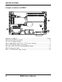
Table of Contents
Introduction ....................................................... 1
Product Description............................................................. 1
Checklist .............................................................................. 2
IB895 Specifications ........................................................... 3
Board Dimensions ............................................................... 4
Installations ....................................................... 5
Installing the Memory ......................................................... 6
Setting the Jumpers ............................................................. 7
Connectors on IB895......................................................... 11
BIOS Setup ....................................................... 19
Drivers Installation ...................................... 39
Intel Chipset Software Installation Utility ........................ 40
VGA Drivers Installation .................................................. 41
Realtek HD Audio Driver Installation .............................. 42
LAN Drivers Installation................................................... 43
Appendix............................................................ 44
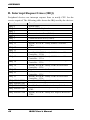
A. I/O Port Address Map .................................................. 44
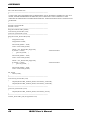
B. Interrupt Request Lines (IRQ) ...................................... 46
C. Digital I/O Sample Code .............................................. 47
D. Watchdog Timer Configuration ................................... 52
IB895 User’s Manual
iii
This page is intentionally left blank.
iv
IB895 User’s Manual
INTRODUCTION
Introduction
Product Description
The IB895 is a 3.5-inch single board computer based on the Intel® Atom
Cedarview chipset. The Cedar Trail is a platform that uses the Intel
Cedarview-D or Cedarview -M Processor and Intel NM10 Express
Chipset family in the desktop platforms.
The role of the processor in the system is to manage the flow of
information between the following interfaces: DDR3 System Memory
interface, DVI display interface, VGA graphics interface, Low Voltage
Differential Signaling (LVDS) and the Direct Media Interface (DMI).
The processor supports single channel, one DDR3 SODIMMs.
®
The Intel processors provide advanced performance in both computing
and graphics quality. This meets the requirement of customers in the
gaming, POS, digital signage and server market segment.
The processor is built on 32-nanometer Hi-K process technology with
Micro-FCBGA11 packaging.
IB895 FEATURES:
Supports Intel® Cedarview -D and Cedarview-M processors
One DDR3 SO-DIMM, 800/1066 MHz, Max. 2GB/4GB
memory*
Integrated Graphics for DVI-I, LVDS displays
2 x SATA Connector
4x COM Port Connector
2 x Mini-PCIe(x1) slot (w/ USB support)
2x GbE (RJ-45) Connector
1x 24V to 12V DC-IN Power Connector
* Note: IB895 with Intel Atom D2550 supports up to 4GB memory
and IB895N with Intel Atom N2600 supports up to 2GB memory.
IB895 User’s Manual
1
INTRODUCTION
Checklist
Your IB895 package should include the items listed below.
The IB895 Embedded Flex Motherboard
This User’s Manual
1 CD containing chipset drivers and flash memory utility
2
IB895 User’s Manual
INTRODUCTION
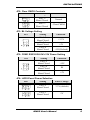
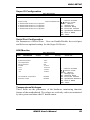
IB895 Specifications
Product Name
Form Factor
CPU
Type/Speed
Chipset
BIOS
Memory
VGA
LVDS
LAN
USB
Serial
Ports
Audio
ATA
LPC I/O
Digital IO
Keyboard/
Mouse Connector
IB895 [default silk screen model # on PCB]
IB895N(N2600 onboard)
3.5”
TM
Intel® Atom DC D2550 / 1MB cache / 1.86 GHz [TDP=10W] (IB895)
Intel® AtomTM DC N2600 / 1MB cache / 1.60 GHz [TDP=3.5W]
(IB895N)
Package = FCBGA437 [ 22 mm x 22 mm] ; Cores / Threads = 2 / 4
®
Intel CG82NM10 PCH [TDP = 2.1W]
Package = BGA360, 17mm x 17 mm
AMI BIOS, support ACPI Function
Intel® Atom TM on-die memory controller
1x DDR3-1066 SO-DIMM socket [Horizontal type]
Maximum memory: 4GB for D2550; 2GB for N2600
Non-ECC, Unbuffered, 1.5V
Intel® GMA 3650 (Gfx freq @ 640MHz) for D2550
Intel® Graphics Media Acc GMA elerator 3600 (Gfx freq @ 400MHz) for
N2600
Supports DirectX 9 Graphics, OpenGL 3.0
DVI-I x 1 (Thru VGA + ASM1422 for DVI-D via D2550 or N2600)
24-bit dual channel via CH7511thru eDP
Intel 82583V PCIe Gigabit LAN x 2
NM10 built-in USB 2.0 host controller, support 6 ports
NM10 built-in SATA II controller, supports 2 ports
Intel® NM10 PCH built-in HD Audio controller + Realtek ALC269QHD
Codec w/class-D speaker amplifier(2.3W per channel @ 5V power
supply) [7mm x 7mm @ 48-QFN] ; support 2-channel audio out + amp
Nuvoton NCT6627UD [128-pin QFP, 14x14x1.4mm]
COM #1 (RS232/422/485) support ring-in with power @500 mA
(selectable for 5V or 12V) [EXAR SP339EER1 232/422/485
transceiver x 1 for jumper-less]
COM #2 (RS232 only)
COM #3 / COM #4 (RS-232 only)
[Hardware Monitor]
2 x Thermal inputs; 2 x Voltage monitoring
1 x Fan Header(DC Fan type)
4 in & 4 out
Pin headers
Expansion
Slots
Edge
Connector
Mini PCI-e socket x 2 (1x Full-sized+1xHalf-sized)
**Full-sized MiniPCIe(1x) support mSATA**
DVI-I, 2x RJ45, 2x USB, COM1
Onboard
Header/Connector
Keyboard/mouse, 4x USB 2.0, 2x DF13 for 24-bit dual channel LVDS,
Audio, speaker, COM2, COM3/4, LPC (80-port card debugging
purpose), 2x Mini PCI-e(1x), smart battery, backlight/brightness control,
2x power connector SATA HDD [JST type]
IB895 User’s Manual
3
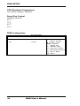
INTRODUCTION
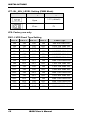
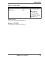
Watchdog
Timer
Power
Connector
Others
[
OS Support
RoHS
Board Size
Yes (256 segments, 0, 1, 2…255 sec/min)
+12V ~ +24V DC-in
- i-Smart function (TI MSP430G2433 MCU)
- AT24C02C EEPROM [SO8 type] via SMbus (Optional)
- Windows 7 (32-bit only)
- Linux
Yes
102mm x 147mm
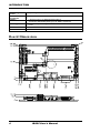
Board Dimensions
4
IB895 User’s Manual
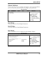
INSTALLATIONS
Installations
This section provides information on how to use the jumpers and
connectors on the IB895 in order to set up a workable system. The topics
covered are:
Installing the Memory ............................................................................ 6
Setting the Jumpers ................................................................................ 7
Connectors on IB895 ........................................................................... 11
IB895 User’s Manual
5
INSTALLATIONS
Installing the Memory
The IB895 board supports one DDR3 memory socket for a maximum
total memory of 2GB or 4GB DDR3 memory type.
Note: IB895 with Intel Atom DC D2550 supports up to 4GB and
IB895N with Intel Atom DC N2600 supports up to 2GB.
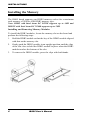
Installing and Removing Memory Modules
To install the DDR3 modules, locate the memory slot on the board and
perform the following steps:
1.
Hold the DDR3 module so that the key of the DDR3 module aligned
with that on the memory slot.
2.
Gently push the DDR3 module in an upright position until the clips
of the slot close to hold the DDR3 module in place when the DDR3
module touches the bottom of the slot.
3.
To remove the DDR3 module, press the clips with both hands.
6
IB895 User’s Manual
INSTALLATIONS
Setting the Jumpers
Jumpers are used on IB895 to select various settings and features
according to your needs and applications. Contact your supplier if you
have doubts about the best configuration for your needs. The following
lists the connectors on IB895 and their respective functions.
Jumper Locations on IB895 ................................................................... 8
JP2: Clear CMOS Contents ................................................................... 9
JP3: BL Voltage Setting ........................................................................ 9
JP5: COM1 RS232 RI/+5V/+12V Power Setting .................................. 9
JP6: LVDS Panel Power Selection ........................................................ 9
JP7: BL_ADJ_LEVEL Setting(PWM Mode) ...................................... 10
JP8: Factory use only ........................................................................... 10
SW1 : LVDS Panel Type setting ......................................................... 10
IB895 User’s Manual
7
INSTALLATIONS
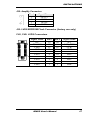
Jumper Locations on IB895
Jumpers on IB895 ............................................................................ Page
JP2: Clear CMOS Contents.................................................................... 9
JP3: BL Voltage Setting......................................................................... 9
JP5: COM1 RS232 RI/+5V/+12V Power Setting .................................. 9
JP6: LVDS Panel Power Selection ........................................................ 9
JP7: BL_ADJ_LEVEL Setting(PWM Mode) ...................................... 10
JP8: Factory use only ........................................................................... 10
SW1 : LVDS Panel Type setting ......................................................... 10
8
IB895 User’s Manual
INSTALLATIONS
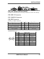
JP2: Clear CMOS Contents
JP2
Setting
Function
Pin 1-2
Short/Closed
Normal
Pin 2-3
Short/Closed
Clear CMOS
JP3: BL Voltage Setting
JP3
Setting
Pin 1-2
Short/Closed
Pin 3-4
Short/Closed
Pin 5-6
Short/Closed
Function
+3.3V
+5V
+12V(Default)
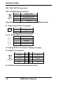
JP5: COM1 RS232 RI/+5V/+12V Power Setting
JP5
Setting
Function
Pin 1-2
Short/Closed
Pin 3-4
Short/Closed
Pin 5-6
Short/Closed
+12V
RI
+5V
JP6: LVDS Panel Power Selection
JP6
Setting
Panel Voltage
Pin 1-2
Short/Closed
3.3V (default)
Pin 2-3
Short/Closed
5V
IB895 User’s Manual
9
INSTALLATIONS
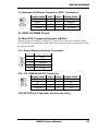
JP7: BL_ADJ_LEVEL Setting (PWM Mode)
JP7
Setting
Voltage
Open
3.3V (default)
Close
5V
JP8: Factory use only
SW1: LVDS Panel Type Setting
SW1-4 SW1-3 SW1-2 SW1-1
10
Panel Type
ON
ON
ON
ON
800*600 18bit 1ch
ON
ON
ON
OFF
1024*768 18bit 1ch
ON
ON
OFF
ON
1024*768 24bit 1ch
ON
ON
OFF
OFF
1280*768 18bit 1ch
ON
OFF
ON
ON
1280*800 18bit 1ch
ON
OFF
ON
OFF
1280*960 18bit 1ch
ON
OFF
OFF
ON
1280*1024 24bit 2ch
ON
OFF
OFF
OFF
1366*768 18bit 1ch
OFF
ON
ON
ON
1366*768 24bit 1ch
OFF
ON
ON
OFF
1440*900 24bit 2ch
OFF
ON
OFF
ON
1440*1050 24bit 2ch
OFF
ON
OFF
OFF
1600*900 24bit 2ch
OFF
OFF
ON
ON
1680*1050 24bit 2ch
OFF
OFF
ON
OFF
1600*1200 24bit 2ch
OFF
OFF
OFF
ON
1920*1080 24bit 2ch
OFF
OFF
OFF
OFF
1920*1200 24bit 2ch
IB895 User’s Manual
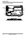
INSTALLATIONS
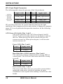
Connectors on IB895
Connector Locations on IB895 ............................................................ 12
CN4, CN5: Gigabit LAN (Intel 82583V) ............................................ 13
CN6: USB 1/2 Connector .................................................................... 13
CN7: VGA DVI-I Connector ............................................................... 13
CN8: DB9 Connector .......................................................................... 13
CN1, CN3: SATA Connector .............................................................. 14
CN2: LCD Backlight Connector .......................................................... 14
J1: Board Input Power Connector ........................................................ 14
J2, J3: SATA HDD Power Connector ................................................. 14
J5: Digital I/O Connector..................................................................... 14
J6: SPI Flash Connector (factory use only).......................................... 14
J7: Keyboard & Mouse Connector (DF11 Connector) ........................ 15
J11: Smart Battery Interface Connector ............................................... 15
J12, J13: USB3/4/5/6/7/8 Connector ................................................... 15
J15: COM3, COM4 Serial Port (DF11 Connector) ............................. 16
J16: COM2/RS232 Serial Port ............................................................ 16
J18: Audio Connector (DF11 Connector) ............................................ 16
J22: Amplify Connector ....................................................................... 17
J23: LVDS EEPROM Flash Connector (factory use only) .................. 17
CH1, CH2: LVDS Connectors............................................................. 17
JP1: Front Panel Connector ................................................................. 18
IB895 User’s Manual
11
INSTALLATIONS
Connector Locations on IB895
12
IB895 User’s Manual
INSTALLATIONS
CN4, CN5: Gigabit LAN (Intel 82583V)
This RJ45 LAN connector (CN4 only) features for EUP LAN wakeup.
CN6: USB 1/2 Connector
CN7: VGA DVI-I Connector
CN8: DB9 Connector
(COM1) is a DB-9 connector.
Signal Name
Pin # Pin #
Signal Name
DCD, Data carrier detect
1
6
DSR, Data set ready
RXD, Receive data
2
7
RTS, Request to send
TXD, Transmit data
3
8
CTS, Clear to send
DTR, Data terminal ready
4
9
RI, Ring indicator
GND, ground
5
10
Not Used
COM1 is jumper-less for RS-232, RS-422 and RS-485 and configured
with BIOS Selection.
Pin #
Signal Name
RS-232
R2-422
RS-485
[
1
2
3
4
5
6
7
8
9
10
DCD
RX
TX
DTR
Ground
DSR
RTS
CTS
RI
NC
RX+
RXTX+
TXGround
NC
NC
NC
NC
NC
IB895 User’s Manual
DATADATA+
NC
NC
Ground
NC
NC
NC
NC
NC
13
INSTALLATIONS
CN1, CN3: SATA Connectors
CN2: LCD Backlight Connector
Pin #
Signal Name
1
Backlight Power
2
Backlight Enable
3
Brightness Control
4
Ground
Note: Brightness Control only support PWM-Mode Panel
J1: Board Input Power Connector
1
Pin #
1
2
Signal Name
+12V to +24V
GND
J2, J3: SATA HDD Power Connector
Pin #
Signal Name
1
+5V
2
Ground
3
Ground
4
+12V
J4: Debug 80 Port Connector (factory use only)
J5: Digital I/O Connector
Signal Name Pin
GND
1
OUT3
3
OUT2
5
IN3
7
IN2
9
Pin
2
4
6
8
10
Signal Name
VCC
OUT1
OUT0
IN1
IN0
J6: SPI Flash Connector (factory use only)
14
IB895 User’s Manual
INSTALLATIONS
J7: Keyboard & Mouse Connector (DF11 Connector)
Signal Name
VCC
MDA
MCL
Ground
Pin #
1
3
5
7
Pin #
2
4
6
8
Signal Name
VCC
KBDA
KBCL
Ground
J8: DDR3 SO-DIMM Socket
J9: Mini PCIE Connector(Support mSATA)
J9 also supports mSATA. However, when J9 is used for mSATA, then
CN3 SATA port cannot be used. Only one of them can be used at one time
to support SATA.
J11: Smart Battery Interface Connector
Pin #
Signal Name
1
RST
2
EXTSMI
3
Ground
4
DATA
5
CLK
J12, J13: USB3/4/5/6/7/8 Connector
Signal Name Pin # Pin #
Vcc
1
2
D3
4
D+
5
6
Ground
7
8
Signal Name
Ground
D+
DVcc
J14: MCU Flash Connector (factory use only)
IB895 User’s Manual
15
INSTALLATIONS
J15: COM3, COM4 Serial Port (DF11 Connector)
Signal Name
DSR3
RTS3
CTS3
RI3
NC
DSR4
RTS4
CTS4
RI4
NC
Pin #
2
4
6
8
10
12
14
16
18
20
Pin #
1
3
5
7
9
11
13
15
17
19
Signal Name
DCD3
RXD3
TXD3
DTR3
Ground
DCD4
RXD4
TXD4
DTR4
Ground
Pin #
2
4
6
8
10
Signal Name
RXD, Receive data
DTR, Data terminal ready
DSR, Data set ready
CTS, Clear to send
Not Used
J16: COM2/RS232 Serial Port
Signal Name
DCD, Data carrier detect
TXD, Transmit data
GND, ground
RTS, Request to send
RI, Ring indicator
Pin #
1
3
5
7
9
J17: Mini PCIE Connector
J18: Audio Connector (DF11 Connector)
Signal Name Pin # Pin #
LINEOUT_R
2
1
Ground
4
3
LINEIN_R
6
5
Ground
8
7
MIC-R
10
9
Ground
12
11
16
IB895 User’s Manual
Signal Name
LINEOUT_L
JD_FRONT
LINEIN_L
JD_LINEIN
MIC_L
JD_MIC1
INSTALLATIONS
J22: Amplify Connector
Pin #
1
2
3
4
Signal Name
OUTL+
OUTLOUTROUTR+
J23: LVDS EEPROM Flash Connector (factory use only)
CH1, CH2: LVDS Connectors
Signal Name
N.C
ENABLE
CLK+
GND
LD2+
LD3+
GND
LD1+
GND
LD0+
Pin #
19
17
15
13
11
9
7
5
3
1
Pin #
20
18
16
14
12
10
8
6
4
2
IB895 User’s Manual
Signal Name
N.C
LCD_PWR
CLKGND
LD2LD3LCD_PWR
LD1GND
LD0-
17
INSTALLATIONS
JP1: Front Panel Connector
The following table shows the pin outs of the 2x4 pin header
Signal Name
Ground
PWR_LED+
Pin #
1
3
Pin #
2
4
HDD_LED+
Ground
5
7
6
8
Signal Name
PWR_SW
PWR_LED-(GND
)
HDD_LEDRESET
JP1 provides connectors for system indicators that provide light
indication of the computer activities and switches to change the computer
status. JP1 is an 8-pin header that provides interfaces for the following
functions.
ATX Power ON Switch: Pins 1 and 2
This 2-pin connector is an “ATX Power Supply On/Off
Switch” on the system that connects to the power switch on
the case. When pressed, the power switch will force the
system to power on. When pressed again, it will force the
system to power off.
Power LED: Pins 3 and 4
Pin #
3
4
Signal Name
LED(+)
LED(-)
Hard Disk Drive LED Connector: Pins 5 and 6
This connector connects to the hard drive activity LED on
control panel. This LED will flash when the HDD is being
accessed.
Pin #
5
6
Signal Name
LED(+)
LED(-)
Reset Switch: Pins 7 and 8
The reset switch allows the user to reset the system without
turning the main power switch off and then on again.
Orientation is not required when making a connection to this
header.
18
IB895 User’s Manual
BIOS SETUP
BIOS Setup
This chapter describes the different settings available in the AMI BIOS
that comes with the board. The topics covered in this chapter are as
follows:
BIOS Introduction ........................................................................................ 20
BIOS Setup .................................................................................................... 20
Advanced Settings ........................................................................................ 22
Chipset Settings............................................................................................. 31
Boot Settings ................................................................................................. 36
Security Settings ........................................................................................... 37
Save & Exit Settings..................................................................................... 38
IB895 User’s Manual
19
BIOS SETUP
BIOS Introduction
The BIOS (Basic Input/Output System) installed in your computer
system’s ROM supports Intel processors. The BIOS provides critical
low-level support for a standard device such as disk drives, serial ports
and parallel ports. It also password protection as well as special support
for detailed fine-tuning of the chipset controlling the entire system.
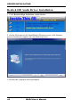
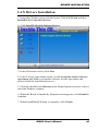
BIOS Setup
The BIOS provides a Setup utility program for specifying the system
configurations and settings. The BIOS ROM of the system stores the
Setup utility. When you turn on the computer, the BIOS is immediately
activated. Pressing the <Del> key immediately allows you to enter the
Setup utility. If you are a little bit late pressing the <Del> key, POST
(Power On Self Test) will continue with its test routines, thus preventing
you from invoking the Setup. If you still wish to enter Setup, restart the
system by pressing the ”Reset” button or simultaneously pressing the
<Ctrl>, <Alt> and <Delete> keys. You can also restart by turning the
system Off and back On again. The following message will appear on the
screen:
Press
<DEL>
to
Enter
Setup
In general, you press the arrow keys to highlight items, <Enter> to select,
the <PgUp> and <PgDn> keys to change entries, <F1> for help and
<Esc> to quit.
When you enter the Setup utility, the Main Menu screen will appear on
the screen. The Main Menu allows you to select from various setup
functions and exit choices.
20
IB895 User’s Manual
BIOS SETUP
Warning: It is strongly recommended that you avoid making any
changes to the chipset defaults. These defaults have been
carefully chosen by both AMI and your system manufacturer
to provide the absolute maximum performance and
reliability. Changing the defaults could cause the system to
become unstable and crash in some cases.
System Date
Set the Date. Use Tab to switch between Data elements.
System Time
Set the Time. Use Tab to switch between Data elements.
IB895 User’s Manual
21
BIOS SETUP
Advanced Settings
This section allows you to configure and improve your system and allows
you to set up some system features according to your preference.
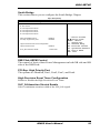
Aptio Setup Utility
Main
Advanced
Chipset
Legacy OpROM Support
Launch PXE OpROM
Boot
Security
Save & Exit
Disabled
► PCI Subsystem Settings
► ACPI Settings
► Wake up event setting
► CPU Configuration
► iSmart Configuration
► IDE Configuration
→ ← Select
► USB Configuration
► W83627UHG Super IO Configuration
► H/W Monitor
► PPM Configuration
Screen
↑↓ Select Item
Enter: Select
+- Change Opt
F1: General Help
F2: Previous Values
F3: Optimized Default
F4: Save & EXIT
ESC: Exit
Launch PXE OpROM
Enable or Disable Boot Option for Legacy Network Devices.
22
IB895 User’s Manual
BIOS SETUP
PCI Subsystem Settings
Aptio Setup Utility
Main
Advanced
Chipset
Boot
PCI Bus Driver Version
V 2.05.01
PCI ROM Priority
Legacy ROM
PCI Common Settings
PCI Latency Timer
VGA Palette Snoop
PERR# Generation
SERR# Generation
32 PCI Bus Clocks
Disabled
Disabled
Disabled
Security
Save & Exit
→ ← Select
Screen
↑↓ Select Item
Enter: Select
+- Change Opt
F1: General Help
F2: Previous Values
F3: Optimized Default
F4: Save & EXIT
ESC: Exit
PCI ROM Priority
In case of multiple Option ROMs (Legacy and EFI Compatible), specifies what
PCI Option ROM to launch.
PCI Latency Timer
Value to be programmed into PCI Latency Timer Register.
VGA Palette Snoop
Enables or Disables VGA Palette Registers Snooping.
PERR# Generation
Enables or Disables PCI Device to Generate PERR#.
SERR# Generation
Enables or Disables PCI Device to Generate SERR#.
IB895 User’s Manual
23
BIOS SETUP
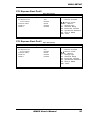
ACPI Settings
Aptio Setup Utility
Main
Advanced
Chipset
Boot
Security
Save & Exit
ACPI Settings
→ ← Select
Enable ACPI Auto Configuration
Disabled
Enabled ACPI Auto Configuration
Enables or Disables BIOS ACPI Auto Configuration.
24
IB895 User’s Manual
Screen
↑↓ Select Item
Enter: Select
+- Change Opt
F1: General Help
F2: Previous Values
F3: Optimized Default
F4: Save & EXIT
ESC: Exit
BIOS SETUP
Wake up event setting
Aptio Setup Utility
Main
Advanced
Wake on Ring
Wake on PCIE PME
Chipset
Boot
Security
Disabled
Disabled
Save & Exit
→ ← Select
Screen
↑↓ Select Item
Enter: Select
+- Change Opt
F1: General Help
F2: Previous Values
F3: Optimized Default
F4: Save & EXIT
ESC: Exit
Wake on Ring
The options are Disabled and Enabled.
Wake on PCIE PME
The options are Disabled and Enabled.
IB895 User’s Manual
25
BIOS SETUP
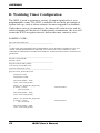
CPU Configuration
This section shows the CPU configuration parameters.
Aptio Setup Utility
Main
Advanced
Chipset
Boot
Security
Save & Exit
CPU Configuration
Processor Type
EMT64
Processor Speed
System Bus Speed
Ratio Status
Intel(R) Atom(TM) CPU
Supported
1865 MHz
533 MHz
14
Actual Ratio
System Bus Speed
Processor Stepping
Microcode Revision
L1 Cache RAM
L2 Cache RAM
Processor Core
Hyper-Threading
14
533 MHz
30661
269
2x56 k
2x512 k
Dual
Supported
Hyper-Threading
Execute Disable Bit
Limit CPUID Maximum
Enabled
Enabled
Disabled
→ ← Select
Screen
↑↓ Select Item
Enter: Select
+- Change Opt
F1: General Help
F2: Previous Values
F3: Optimized Default
F4: Save & EXIT
ESC: Exit
Hyper-threading
Enabled for Windows XP and Linux (OS optimized for Hyper-Threading
Technology) and Disabled for other OS (OS not optimized for
Hyper-Threading Technology). When Disabled, only one thread per
enabled core is enabled.
Execute Disable Bit
XD can prevent certain classes of malicious buffer overflow attacks when
combined with a supporting OS (Windows Server 2003 SP1, Windows
XP SP2, SuSE Linux 9.2, Re33dHat Enterprise 3 Update 3.)
Limit CPUID Maximum
Disabled for Windows XP.
26
IB895 User’s Manual
BIOS SETUP
iSmart Controller
Aptio Setup Utility
Main
Advanced
Chipset
Boot
Security
Save & Exit
→ ←
iSmart Controller
EuP/ErP standby power Control
Power-On after Power failure
Keep standby power
Disable
Schedule Slot 1
Schedule Slot 2
None
None
Select Screen
↑↓ Select Item
Enter: Select
+- Change Opt
F1: General Help
F2: Previous Values
F3: Optimized Default
F4: Save & EXIT
ESC: Exit
EuP/ErP standby power Control
Saving the power consumption on power off.
Power-On after Power failure
This field sets the system power status whether on or off when power
returns to the system from a power failure situation.
Schedule Slot
None / Power On / Power On/Off – Setup the hour/minute for system
power on
IDE Configuration
Aptio Setup Utility
Main
Advanced
Chipset
Boot
Security
Save & Exit
→ ←
SATA Port0
SATA Port1
Not Present
Not Present
SATA Controller(s)
Enabled
Configure SATA as
IDE
Select Screen
↑↓ Select Item
Enter: Select
+- Change Opt
F1: General Help
F2: Previous Values
F3: Optimized Default
F4: Save & EXIT
ESC: Exit
SATA Controller(s)
Enable / Disable Serial ATA Controller.
Configure SATA as
(1) IDE Mode.
(2) AHCI Mode.
IB895 User’s Manual
27
BIOS SETUP
USB Configuration
Aptio Setup Utility
Main
Advanced
Chipset
Boot
Security
Save & Exit
USB Configuration
→ ← Select
USB Devices:
None
Legacy USB Support
EHCI Hand-off
Enabled
Enabled
USB hardware delays and time-outs:
USB Transfer time-out
20 sec
Device reset time-out
Device power-up delay
20 sec
Auto
Screen
↑↓ Select Item
Enter: Select
+- Change Opt
F1: General Help
F2: Previous Values
F3: Optimized Default
F4: Save & EXIT
ESC: Exit
Legacy USB Support
Enables Legacy USB support.
AUTO option disables legacy support if no USB devices are connected.
DISABLE option will keep USB devices available only for EFI
applications.
EHCI Hand-off
Enabled/Disabled. This is a workaround for OSes without EHCI hand-off
support. The EHCI ownership change should be claimed by EHCI driver.
USB Transfer time-out
The time-out value for Control, Bulk, and Interrupt transfers.
Device reset time-out
USB mass Storage device start Unit command time-out.
Device power-up delay
Maximum time the device will take before it properly reports itself to the
Host Controller. ‘Auto’ uses default value: for a Root port it is 100ms, for
a Hub port the delay is taken from Hub descriptor.
28
IB895 User’s Manual
BIOS SETUP
Super IO Configuration
Aptio Setup Utility
Main
Advanced
Chipset
Boot
Security
Save & Exit
W83627UHG Super IO Configuration
→ ← Select
Super IO Chip
Winbond W83627UHG
► W83627UHG Serial Port 0 Configuration
► W83627UHG Serial Port 1 Configuration
► W83627UHG Serial Port 2 Configuration
► W83627UHG Serial Port 3 Configuration
Screen
↑↓ Select Item
Enter: Select
+- Change Opt
F1: General Help
F2: Previous Values
F3: Optimized Default
F4: Save & EXIT
ESC: Exit
Serial Port Configuration
Set Parameters of Serial Ports. User can Enable/Disable the serial port
and Select an optimal settings for the Super IO Device.
H/W Monitor
Aptio Setup Utility
Main
Advanced
Chipset
Boot
Security
Save & Exit
Pc Health Status
System temperature
CPU temperature
CPU Fan Speed
VCORE
+12V
+50 C
+55 C
N/A
+1.184 V
+12.032 V
+3.3V
+5V
+3.248 V
+4.960 V
CPU Shutdown Temperature
SmartFan Control
Disabled
Disabled
→ ← Select
Screen
↑↓ Select Item
Enter: Select
+- Change Opt
F1: General Help
F2: Previous Values
F3: Optimized Default
F4: Save & EXIT
ESC: Exit
Temperatures/Voltages
These fields are the parameters of the hardware monitoring function
feature of the motherboard. The values are read-only values as monitored
by the system and show the PC health status.
IB895 User’s Manual
29
BIOS SETUP
CPU Shutdown Temperature
The default setting is Disabled.
Smart Fan Control
Disabled (default)
60 ℃
70 ℃
80 ℃
90 ℃
PPM Configuration
Aptio Setup Utility
Main
Advanced
Chipset
Boot
Security
Save & Exit
PPM Configuration
→ ← Select
EIST
30
Enabled
IB895 User’s Manual
Screen
↑↓ Select Item
Enter: Select
+- Change Opt
F1: General Help
F2: Previous Values
F3: Optimized Default
F4: Save & EXIT
ESC: Exit
BIOS SETUP
Chipset Settings
This section allows you to configure and improve your system and allows
you to set up some system features according to your preference.
Aptio Setup Utility
Main
Advanced
Chipset
Boot
Security
Save & Exit
► Host Bridge
→ ← Select
► South Bridge
Screen
↑↓ Select Item
Enter: Select
+- Change Field
F1: General Help
F2: Previous Values
F3: Optimized Default
F4: Save
ESC: Exit
Host Bridge
This item shows the Host Bridge Parameters.
South Bridge
This item shows the South Bridge Parameters.
Host Bridge
This section allows you to configure the Host Bridge Chipset.
Aptio Setup Utility
Main
Chipset
Advanced
Boot
Security
Save & Exit
► Memory Frequency and Timing
→ ←
► Intel IGD Configuration
************Memory Information************
Memory Frequency
1067 MHz(DDR3)
Total Memory
DIMM#1
2048 MB
2048 MB
IB895 User’s Manual
Select Screen
↑↓ Select Item
Enter: Select
+- Change Opt
F1: General Help
F2: Previous Values
F3: Optimized Default
F4: Save & EXIT
ESC: Exit
31
BIOS SETUP
Memory Frequency and Timing
Aptio Setup Utility
Main
Advanced
Chipset
Boot
Security
Save & Exit
Memory Frequency and Timing
MRC Fast Boot
Max TOLUD
Enabled
Dynamic
→ ← Select
Screen
↑↓ Select Item
Enter: Select
+- Change Opt
F1: General Help
F2: Previous Values
F3: Optimized Default
F4: Save & EXIT
ESC: Exit
MRC Fast Boot
The options are Disabled and Enabled.
Max TOLUD
The default setting is Dynamic.
Intel IGD Configuration
Aptio Setup Utility
Main
Advanced
Intel IGD Configuration
IGFX-Boot Type
LVDS Back Light Control
Chipset
Boot
Security
Save & Exit
VBIOS Default
7(MAX)
→ ← Select
Screen
↑↓ Select Item
Enter: Select
+- Change Opt
F1: General Help
F2: Previous Values
F3: Optimized Default
F4: Save & EXIT
ESC: Exit
IGFX-Boot Type
Select the video Device which will be activated during POST .
32
IB895 User’s Manual
BIOS SETUP
South Bridge
This section allows you to configure the South Bridge Chipset.
Aptio Setup Utility
Main
Advanced
Chipset
Boot
Security
Save & Exit
► TPT Device
► PCI Express Root Port0
► PCI Express Root Port1
► PCI Express Root Port2
► PCI Express Root Port3
DMI Link ASPM Control
Enabled
PCI-Exp. High Priority Port
Disabled
High Precision Event Timer Configuration
High Precision Timer
Enabled
SLP_SP4 Assertion Width
1-2 Seconds
→ ← Select
Screen
↑↓ Select Item
Enter: Select
+- Change Opt
F1: General Help
F2: Previous Values
F3: Optimized Default
F4: Save & EXIT
ESC: Exit
DMI Clink ASPM Control
The control of Active State Power Management on both NB side and SB
side of the DMI Link.
PCI-Exp. High Priority Port
The options are Disabled, Port1, Port2, Port3, and Port4.
High Precision Event Timer Configuration
Enable/or Disable the High Precision Event Timer.
SLP_S4 Assertion Stretch Enable
Select a minimum assertion width of the SLP_S4# signal.
IB895 User’s Manual
33
BIOS SETUP
TPT Device
Aptio Setup Utility
Main
Advanced
Chipset
Azalia Controller
Select USB Mode
UHCI #1 (port 0 and 1)
UHCI #2 (port 2 and 3)
UHCI #3 (port 4 and 5)
UHCI #4 (port 6 and 7)
USB 2.0(EHCI) Support
Boot
Security
Save & Exit
HD Audio
→ ← Select
By Controllers
Enabled
Enabled
Enabled
Enabled
Enabled
↑↓ Select Item
Enter: Select
+- Change Opt
F1: General Help
F2: Previous Values
F3: Optimized Default
F4: Save & EXIT
ESC: Exit
Screen
PCI Express Root Port0
Aptio Setup Utility
Main
Advanced
Chipset
Boot
PCI Express Port 0
Port 0 IOxAPIC
Automatic ASPM
Enabled
Disabled
Manual
ASPM L0s
ASPM L1
Root Port Only
Enabled
Security
Save & Exit
→ ← Select
Screen
↑↓ Select Item
Enter: Select
+- Change Opt
F1: General Help
F2: Previous Values
F3: Optimized Default
F4: Save & EXIT
ESC: Exit
PCI Express Root Port1
Aptio Setup Utility
Main
Advanced
PCI Express Port 0
Port 0 IOxAPIC
Automatic ASPM
ASPM L0s
ASPM L1
34
Chipset
Boot
Security
Auto
Disabled
Manual
Root Port Only
Enabled
IB895 User’s Manual
Save & Exit
→ ← Select
Screen
↑↓ Select Item
Enter: Select
+- Change Opt
F1: General Help
F2: Previous Values
F3: Optimized Default
F4: Save & EXIT
ESC: Exit
BIOS SETUP
PCI Express Root Port2
Aptio Setup Utility
Main
Advanced
Chipset
PCI Express Port 2
Port 0 IOxAPIC
Automatic ASPM
ASPM L0s
ASPM L1
Boot
Security
Save & Exit
→ ← Select
Auto
Disabled
Manual
Disabled
Disabled
Screen
↑↓ Select Item
Enter: Select
+- Change Opt
F1: General Help
F2: Previous Values
F3: Optimized Default
F4: Save & EXIT
ESC: Exit
PCI Express Root Port3
Aptio Setup Utility
Main
Advanced
PCI Express Port 3
Port 0 IOxAPIC
Automatic ASPM
ASPM L0s
ASPM L1
Chipset
Boot
Security
Auto
Disabled
Manual
Disabled
Disabled
IB895 User’s Manual
Save & Exit
→ ← Select
Screen
↑↓ Select Item
Enter: Select
+- Change Opt
F1: General Help
F2: Previous Values
F3: Optimized Default
F4: Save & EXIT
ESC: Exit
35
BIOS SETUP
Boot Settings
Aptio Setup Utility
Main
Advanced
Chipset
Boot
Security
Boot Configuration
Setup Prompt Timeout
Bootup NumLock State
1
On
Quiet Boot
Fast Boot
Disabled
Disabled
CSM16 Module Version
07.68
GateA20 Active
Upon Request
Option ROM Messages
Interrupt 19 Canture
CSM Support
Force BIOS
Enabled
Enabled
Save & Exit
→ ← Select
Screen
↑↓ Select Item
Enter: Select
+- Change Opt
F1: General Help
F2: Previous Values
F3: Optimized Default
F4: Save & EXIT
ESC: Exit
Boot Option Priorities
Setup Prompt Timeout
Number of seconds to wait for setup activation key.
65535(0xFFFF) means indefinite waiting.
Bootup NumLock State
Select the keyboard NumLock state.
Quiet Boot
Enables/Disables Quiet Boot option.
Fast Boot
Enables/Disables boot with initialization of a minimal set of devices
required to launch active boot option. Has no effect for BBS boot options.
GateA20 Active
UPON REQUEST – GA20 can be disabled using BIOS services.
ALWAYS – do not allow disabling GA20; this option is useful when any RT
code is executed above 1MB.
Option ROM Messages
Set display mode for Option ROM. Options: Force BIOS; Keep Current.
Interrupt 19 Capture
Enable: Allows Option ROMs to trap Int 19.
CSM Support
Enables/Disables/Auto CSM Support.
36
IB895 User’s Manual
BIOS SETUP
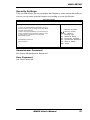
Security Settings
This section allows you to configure and improve your system and allows
you to set up some system features according to your preference.
Aptio Setup Utility
Main
Advanced
Chipset
Boot
Security
Save & Exit
Password Description
If ONLY the Administrator’s password is set, then
this only limits access to Setup and is only asked
for when entering Setup.
If ONLY the User’s password is set, then this is a
power on password and must be entered to boot
or enter Setup. In Setup the User will have
Administrator rights
Administrator Password
User Password
→ ← Select
Screen
↑↓ Select Item
Enter: Select
+- Change Opt
F1: General Help
F2: Previous Values
F3: Optimized Default
F4: Save & EXIT
ESC: Exit
Administrator Password
Set Setup Administrator Password.
User Password
Set User Password.
IB895 User’s Manual
37
BIOS SETUP
Save & Exit Settings
Aptio Setup Utility
Main
Advanced
Chipset
Boot
Security
Save Changes and Exit
Discard Changes and Exit
Save Changes and Reset
Discard Changes and Reset
Save & Exit
→ ← Select
Save Options
Save Changes
Discard Changes
Restore Defaults
Save as User Defaults
Restore User Defaults
Boot Override
Save Changes and Exit
Exit system setup after saving the changes.
Discard Changes and Exit
Exit system setup without saving any changes.
Save Changes and Reset
Reset the system after saving the changes.
Discard Changes and Reset
Reset system setup without saving any changes.
Save Changes
Save Changes done so far to any of the setup options.
Discard Changes
Discard Changes done so far to any of the setup options.
Restore Defaults
Restore/Load Defaults values for all the setup options.
Save as User Defaults
Save the changes done so far as User Defaults.
Restore User Defaults
Restore the User Defaults to all the setup options.
38
Screen
↑↓ Select Item
Enter: Select
+- Change Opt
F1: General Help
F2: Previous Values
F3: Optimized Default
F4: Save & EXIT
ESC: Exit
IB895 User’s Manual
DRIVER INSTALLATION
Drivers Installation
This section describes the installation procedures for software and
drivers. The software and drivers are included with the motherboard. If
you find the items missing, please contact the vendor where you made the
purchase. The contents of this section include the following:
Intel Chipset Software Installation Utility ........................................... 40
VGA Drivers Installation ..................................................................... 41
Realtek HD Audio Driver Installation ................................................. 42
LAN Drivers Installation ..................................................................... 43
IMPORTANT NOTE:
After installing your Windows operating system, you must install first the
Intel Chipset Software Installation Utility before proceeding with the
drivers installation.
IB895 User’s Manual
39
DRIVER INSTALLATION
Intel Chipset Software Installation Utility
The Intel Chipset Drivers should be installed first before the software
drivers to enable Plug & Play INF support for Intel chipset components.
Follow the instructions below to complete the installation.
1. Insert the disc that comes with the board. Click Intel and then Intel(R)
Cedarview Chipset Drivers.
2. Click Intel(R) Chipset Software Installation Utility.
3. When the Welcome screen to the Intel® Chipset Device Software
appears, click Next to continue.
4. Click Yes to accept the software license agreement and proceed with
the installation process.
5. On the Readme File Information screen, click Next to continue the
installation.
6. The Setup process is now complete. Click Finish to restart the
computer and for changes to take effect.
40
IB895 User’s Manual
DRIVER INSTALLATION
VGA Drivers Installation
IMPORTANT NOTE: After installing the graphics driver, the default
display is still LVDS. Both VGA/CRT and DVI will only be extended
displays. To switch to any of these displays, use the hot key:
For VGA – Ctrl+Alt+F1
For DVI – Ctrl+Alt+F3
1. Click Intel(R) Cedarview Graphics Driver.
2. When the Welcome screen appears, click Next to continue.
4. Click Yes to to agree with the license agreement and continue the
installation.
5. On the Readme File Information screen, click Next to continue the
installation of the Intel® Graphics Media Accelerator Driver.
6. On Setup Progress screen, click Next to continue.
7. Setup complete. Click Finish to restart the computer and for changes
to take effect.
IB895 User’s Manual
41
DRIVER INSTALLATION
Realtek HD Audio Driver Installation
1. Click Realtek High Definition Audio Driver.
2. On the Welcome to the InstallShield Wizard screen, click Next to
proceed with and complete the installation process.
3. Restart the computer when prompted.
42
IB895 User’s Manual
DRIVER INSTALLATION
LAN Drivers Installation
1. Insert the CD that comes with the board. Click LAN Card and then
Intel(R) LAN Controller Drivers.
2. Click Intel(R) Gigabit Ethernet Drivers.
3. In the Welcome screen, click Next.
4. In the License Agreement screen, click I accept the terms in license
agreement and Next to accept the software license agreement and
proceed with the installation process.
5. Click the checkbox for Drivers in the Setup Options screen to select it
and click Next to continue.
6. When the Ready to Install the Program screen appears, click Install to
continue.
7. When InstallShield Wizard is complete, click Finish.
IB895 User’s Manual
43
APPENDIX
Appendix
A. I/O Port Address Map
Each peripheral device in the system is assigned a set of I/O port
addresses which also becomes the identity of the device. The following
table lists the I/O port addresses used.
Address
0000-001F
0000-001F
0020-0021
0024-0025
0028-0029
002C-002D
0030-0031
0034-0035
0038-0039
003C-003D
0040-0043
0050-0053
0060-0060
0064-0064
0070-0077
0081-0091
0093-009F
00A0-00A1
00A4-00A5
00A8-00A9
00AC-00AD
00B0-00B1
00B4-00B5
00B8-00B9
00BC-00BD
00C0-00DF
00F0-00F0
02E8-02EF
02F8-02FF
44
Device Description
Direct memory access controller
PCI bus
Programmable interrupt controller
Programmable interrupt controller
Programmable interrupt controller
Programmable interrupt controller
Programmable interrupt controller
Programmable interrupt controller
Programmable interrupt controller
Programmable interrupt controller
System timer
System timer
Standard PS/2 Keyboard
Standard PS/2 Keyboard
System CMOS/real time clock
Direct memory access controller
Direct memory access controller
Programmable interrupt controller
Programmable interrupt controller
Programmable interrupt controller
Programmable interrupt controller
Programmable interrupt controller
Programmable interrupt controller
Programmable interrupt controller
Programmable interrupt controller
Direct memory access controller
Numeric data processor
Communications Port (COM4)
Communications Port (COM2)
IB895 User’s Manual
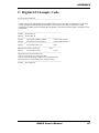
APPENDIX
Address
03B0-03BB
03C0-03DF
03E8-03EF
03F8-03FF
04D0-04D1
0D00-FFFF
D000-DFFF
E000-EFFF
F000-F01F
F020-F03F
F040-F05F
F060-F07F
F080-F09F
F0A0-F0AF
F0B0-F0B3
F0C0-F0C7
F0D0-F0D3
F0E0-F0E7
F0F0-F0F7
Device Description
Intel(R) Graphics Media Accelerator 3600
Series
Intel(R) Graphics Media Accelerator 3600
Series
Communications Port (COM3)
Communications Port (COM1)
Programmable interrupt controller
PCI bus
Intel(R) N10/ICH7 Family PCI Express
Root Port - 27D2
Intel(R) N10/ICH7 Family PCI Express
Root Port - 27D0
Intel(R) N10/ICH7 Family SMBus
Controller - 27DA
Intel(R) N10/ICH7 Family USB
Universal Host Controller - 27CB
Intel(R) N10/ICH7 Family USB
Universal Host Controller - 27CA
Intel(R) N10/ICH7 Family USB
Universal Host Controller - 27C9
Intel(R) N10/ICH7 Family USB
Universal Host Controller - 27C8
Intel(R) N10/ICH7 Family Serial ATA
Storage Controller - 27C0
Intel(R) N10/ICH7 Family Serial ATA
Storage Controller - 27C0
Intel(R) N10/ICH7 Family Serial ATA
Storage Controller - 27C0
Intel(R) N10/ICH7 Family Serial ATA
Storage Controller - 27C0
Intel(R) N10/ICH7 Family Serial ATA
Storage Controller - 27C0
Intel(R) Graphics Media Accelerator 3600
Series
IB895 User’s Manual
45
APPENDIX
B. Interrupt Request Lines (IRQ)
Peripheral devices use interrupt request lines to notify CPU for the
service required. The following table shows the IRQ used by the devices.
Level
IRQ 0
IRQ 1
IRQ 3
IRQ 4
IRQ 5
IRQ 7
IRQ 8
IRQ 11
IRQ 12
IRQ 13
IRQ 16
IRQ 18
IRQ 19
IRQ 19
IRQ 22
IRQ 23
IRQ 23
IRQ 4294967290
IRQ 4294967291
IRQ 4294967292
IRQ 4294967293
IRQ 4294967294
46
Function
System timer
Standard PS/2 Keyboard
Communications Port (COM2)
Communications Port (COM1)
Communications Port (COM3)
Communications Port (COM4)
System CMOS/real time clock
Intel(R) N10/ICH7 Family SMBus Controller 27DA
Microsoft PS/2 Mouse
Numeric data processor
Intel(R) N10/ICH7 Family USB Universal Host
Controller - 27CB
Intel(R) N10/ICH7 Family USB Universal Host
Controller - 27CA
Intel(R) N10/ICH7 Family Serial ATA Storage
Controller - 27C0
Intel(R) N10/ICH7 Family USB Universal Host
Controller - 27C9
High Definition Audio Controller
Intel(R) N10/ICH7 Family USB2 Enhanced Host
Controller - 27CC
Intel(R) N10/ICH7 Family USB Universal Host
Controller - 27C8
Intel(R) 82583V Gigabit Network Connection
Intel(R) 82583V Gigabit Network Connection #2
Intel(R) Graphics Media Accelerator 3600 Series
Intel(R) N10/ICH7 Family PCI Express Root Port 27D2
Intel(R) N10/ICH7 Family PCI Express Root Port 27D0
IB895 User’s Manual
APPENDIX
C. Digital I/O Sample Code
File of the W627UHG.H
//--------------------------------------------------------------------------//
// THIS CODE AND INFORMATION IS PROVIDED "AS IS" WITHOUT WARRANTY OF ANY
// KIND, EITHER EXPRESSED OR IMPLIED, INCLUDING BUT NOT LIMITED TO THE
// IMPLIED WARRANTIES OF MERCHANTABILITY AND/OR FITNESS FOR A PARTICULAR
// PURPOSE.
//
//--------------------------------------------------------------------------#ifndef __W627UHG_H
#define __W627UHG_H
1
//--------------------------------------------------------------------------#define
W627UHG_INDEX_PORT
(W627UHG_BASE)
#define
W627UHG_DATA_PORT
(W627UHG_BASE+1)
//--------------------------------------------------------------------------#define
W627UHG_REG_LD
0x07
//--------------------------------------------------------------------------#define W627UHG_UNLOCK
0x87
#define
W627UHG_LOCK
0xAA
//--------------------------------------------------------------------------unsigned int Init_W627UHG(void);
void Set_W627UHG_LD( unsigned char);
void Set_W627UHG_Reg( unsigned char, unsigned char);
unsigned char Get_W627UHG_Reg( unsigned char);
//--------------------------------------------------------------------------#endif //__W627UHG_H
IB895 User’s Manual
47
APPENDIX
File of the W627UHG.CPP
//--------------------------------------------------------------------------//
// THIS CODE AND INFORMATION IS PROVIDED "AS IS" WITHOUT WARRANTY OF ANY
// KIND, EITHER EXPRESSED OR IMPLIED, INCLUDING BUT NOT LIMITED TO THE
// IMPLIED WARRANTIES OF MERCHANTABILITY AND/OR FITNESS FOR A PARTICULAR
// PURPOSE.
//
//--------------------------------------------------------------------------#include "W627UHG.H"
#include <dos.h>
//--------------------------------------------------------------------------unsigned int W627UHG_BASE;
void Unlock_W627UHG (void);
void Lock_W627UHG (void);
//--------------------------------------------------------------------------unsigned int Init_W627UHG(void)
{
unsigned int result;
unsigned char ucDid;
W627UHG_BASE = 0x4E;
result = W627UHG_BASE;
ucDid = Get_W627UHG_Reg(0x20);
if (ucDid == 0xA2)
{
goto Init_Finish; }
//W83627UHG??
W627UHG_BASE = 0x2E;
result = W627UHG_BASE;
ucDid = Get_W627UHG_Reg(0x20);
if (ucDid == 0xA2)
{
goto Init_Finish; }
//W83627UHG??
W627UHG_BASE = 0x00;
result = W627UHG_BASE;
Init_Finish:
return (result);
}
//--------------------------------------------------------------------------void Unlock_W627UHG (void)
{
outportb(W627UHG_INDEX_PORT, W627UHG_UNLOCK);
outportb(W627UHG_INDEX_PORT, W627UHG_UNLOCK);
}
//--------------------------------------------------------------------------void Lock_W627UHG (void)
{
outportb(W627UHG_INDEX_PORT, W627UHG_LOCK);
}
//--------------------------------------------------------------------------void Set_W627UHG_LD( unsigned char LD)
48
IB895 User’s Manual
APPENDIX
{
Unlock_W627UHG();
outportb(W627UHG_INDEX_PORT, W627UHG_REG_LD);
outportb(W627UHG_DATA_PORT, LD);
Lock_W627UHG();
}
//--------------------------------------------------------------------------void Set_W627UHG_Reg( unsigned char REG, unsigned char DATA)
{
Unlock_W627UHG();
outportb(W627UHG_INDEX_PORT, REG);
outportb(W627UHG_DATA_PORT, DATA);
Lock_W627UHG();
}
//--------------------------------------------------------------------------unsigned char Get_W627UHG_Reg(unsigned char REG)
{
unsigned char Result;
Unlock_W627UHG();
outportb(W627UHG_INDEX_PORT, REG);
Result = inportb(W627UHG_DATA_PORT);
Lock_W627UHG();
return Result;
}
//---------------------------------------------------------------------------
IB895 User’s Manual
49
APPENDIX
File of the MAIN.CPP
//--------------------------------------------------------------------------//
// THIS CODE AND INFORMATION IS PROVIDED "AS IS" WITHOUT WARRANTY OF ANY
// KIND, EITHER EXPRESSED OR IMPLIED, INCLUDING BUT NOT LIMITED TO THE
// IMPLIED WARRANTIES OF MERCHANTABILITY AND/OR FITNESS FOR A PARTICULAR
// PURPOSE.
//
//--------------------------------------------------------------------------#include <dos.h>
#include <conio.h>
#include <stdio.h>
#include <stdlib.h>
#include "W627UHG.H"
//--------------------------------------------------------------------------int main (void);
void Dio5Initial(void);
void Dio5SetOutput(unsigned char);
unsigned char Dio5GetInput(void);
void Dio5SetDirection(unsigned char);
unsigned char Dio5GetDirection(void);
//--------------------------------------------------------------------------int main (void)
{
char SIO;
SIO = Init_W627UHG();
if (SIO == 0)
{
printf("Can not detect Winbond 83627UHG, program abort.\n");
return(1);
}
Dio5Initial();
//for GPIO50..57
Dio5SetDirection(0x0F); //GP50..53 = input, GP54..57=output
printf("Current DIO direction = 0x%X\n", Dio5GetDirection());
printf("Current DIO status = 0x%X\n", Dio5GetInput());
printf("Set DIO output to high\n");
Dio5SetOutput(0x0F);
printf("Set DIO output to low\n");
Dio5SetOutput(0x00);
return 0;
50
IB895 User’s Manual
APPENDIX
}
//--------------------------------------------------------------------------void Dio5Initial(void)
{
unsigned char ucBuf;
Set_W627UHG_LD(0x08);
//enable the GP5 group
ucBuf = Get_W627UHG_Reg(0x30);
ucBuf |= 0x02;
Set_W627UHG_Reg(0x30, ucBuf);
}
//--------------------------------------------------------------------------void Dio5SetOutput(unsigned char NewData)
{
Set_W627UHG_LD(0x08);
Set_W627UHG_Reg(0xE1, NewData);
}
//--------------------------------------------------------------------------unsigned char Dio5GetInput(void)
{
unsigned char result;
Set_W627UHG_LD(0x08);
result = Get_W627UHG_Reg(0xE1);
return (result);
}
//--------------------------------------------------------------------------void Dio5SetDirection(unsigned char NewData)
{
//NewData : 1 for input, 0 for output
Set_W627UHG_LD(0x08);
Set_W627UHG_Reg(0xE0, NewData);
}
//--------------------------------------------------------------------------unsigned char Dio5GetDirection(void)
{
unsigned char result;
Set_W627UHG_LD(0x08);
result = Get_W627UHG_Reg(0xE0);
return (result);
//switch to logic device 8
//switch to logic device 8
//switch to logic device 8
//switch to logic device 8
//switch to logic device 8
}
//---------------------------------------------------------------------------
IB895 User’s Manual
51
APPENDIX
D. Watchdog Timer Configuration
The WDT is used to generate a variety of output signals after a user
programmable count. The WDT is suitable for use in the prevention of
system lock-up, such as when software becomes trapped in a deadlock.
Under these sorts of circumstances, the timer will count to zero and the
selected outputs will be driven. Under normal circumstance, the user will
restart the WDT at regular intervals before the timer counts to zero.
SAMPLE CODE:
File of the W627UHG.CPP
//--------------------------------------------------------------------------//
// THIS CODE AND INFORMATION IS PROVIDED "AS IS" WITHOUT WARRANTY OF ANY
// KIND, EITHER EXPRESSED OR IMPLIED, INCLUDING BUT NOT LIMITED TO THE
// IMPLIED WARRANTIES OF MERCHANTABILITY AND/OR FITNESS FOR A PARTICULAR
// PURPOSE.
//
//--------------------------------------------------------------------------#include "W627UHG.H"
#include <dos.h>
//--------------------------------------------------------------------------unsigned int W627UHG_BASE;
void Unlock_W627UHG (void);
void Lock_W627UHG (void);
//--------------------------------------------------------------------------unsigned int Init_W627UHG(void)
{
unsigned int result;
unsigned char ucDid;
W627UHG_BASE = 0x4E;
result = W627UHG_BASE;
ucDid = Get_W627UHG_Reg(0x20);
if (ucDid == 0xA2)
{
goto Init_Finish; }
//W83627UHG??
W627UHG_BASE = 0x2E;
result = W627UHG_BASE;
ucDid = Get_W627UHG_Reg(0x20);
if (ucDid == 0xA2)
{
goto Init_Finish; }
//W83627UHG??
W627UHG_BASE = 0x00;
result = W627UHG_BASE;
52
IB895 User’s Manual
APPENDIX
Init_Finish:
return (result);
}
//--------------------------------------------------------------------------void Unlock_W627UHG (void)
{
outportb(W627UHG_INDEX_PORT, W627UHG_UNLOCK);
outportb(W627UHG_INDEX_PORT, W627UHG_UNLOCK);
}
//--------------------------------------------------------------------------void Lock_W627UHG (void)
{
outportb(W627UHG_INDEX_PORT, W627UHG_LOCK);
}
//--------------------------------------------------------------------------void Set_W627UHG_LD( unsigned char LD)
{
Unlock_W627UHG();
outportb(W627UHG_INDEX_PORT, W627UHG_REG_LD);
outportb(W627UHG_DATA_PORT, LD);
Lock_W627UHG();
}
//--------------------------------------------------------------------------void Set_W627UHG_Reg( unsigned char REG, unsigned char DATA)
{
Unlock_W627UHG();
outportb(W627UHG_INDEX_PORT, REG);
outportb(W627UHG_DATA_PORT, DATA);
Lock_W627UHG();
}
//--------------------------------------------------------------------------unsigned char Get_W627UHG_Reg(unsigned char REG)
{
unsigned char Result;
Unlock_W627UHG();
outportb(W627UHG_INDEX_PORT, REG);
Result = inportb(W627UHG_DATA_PORT);
Lock_W627UHG();
return Result;
}
//---------------------------------------------------------------------------
IB895 User’s Manual
53
APPENDIX
File of the W627UHG.H
//--------------------------------------------------------------------------//
// THIS CODE AND INFORMATION IS PROVIDED "AS IS" WITHOUT WARRANTY OF ANY
// KIND, EITHER EXPRESSED OR IMPLIED, INCLUDING BUT NOT LIMITED TO THE
// IMPLIED WARRANTIES OF MERCHANTABILITY AND/OR FITNESS FOR A PARTICULAR
// PURPOSE.
//
//--------------------------------------------------------------------------#ifndef __W627UHG_H
#define __W627UHG_H
1
//--------------------------------------------------------------------------#define
W627UHG_INDEX_PORT
(W627UHG_BASE)
#define
W627UHG_DATA_PORT
(W627UHG_BASE+1)
//--------------------------------------------------------------------------#define
W627UHG_REG_LD
0x07
//--------------------------------------------------------------------------#define W627UHG_UNLOCK
0x87
#define
W627UHG_LOCK
0xAA
//--------------------------------------------------------------------------unsigned int Init_W627UHG(void);
void Set_W627UHG_LD( unsigned char);
void Set_W627UHG_Reg( unsigned char, unsigned char);
unsigned char Get_W627UHG_Reg( unsigned char);
//--------------------------------------------------------------------------#endif //__W627UHG_H
54
IB895 User’s Manual
APPENDIX
File of the MAIN.CPP
//--------------------------------------------------------------------------//
// THIS CODE AND INFORMATION IS PROVIDED "AS IS" WITHOUT WARRANTY OF ANY
// KIND, EITHER EXPRESSED OR IMPLIED, INCLUDING BUT NOT LIMITED TO THE
// IMPLIED WARRANTIES OF MERCHANTABILITY AND/OR FITNESS FOR A PARTICULAR
// PURPOSE.
//
//--------------------------------------------------------------------------#include <dos.h>
#include <conio.h>
#include <stdio.h>
#include <stdlib.h>
#include "W627UHG.H"
//--------------------------------------------------------------------------int main (void);
void WDTInitial(void);
void WDTEnable(unsigned char);
void WDTDisable(void);
//--------------------------------------------------------------------------int main (void)
{
char SIO;
SIO = Init_W627UHG();
if (SIO == 0)
{
............................................... printf("Can not detect Winbond 83627UHG, program abort.\n");
.................................................................................................................................... return(1);
}
WDTInitial();
WDTEnable(10);
WDTDisable();
return 0;
}
//--------------------------------------------------------------------------void WDTInitial(void)
{
unsigned char bBuf;
Set_W627UHG_LD(0x08); ................................................................. //switch to logic device 8
bBuf = Get_W627UHG_Reg(0x30);
bBuf &= (~0x01);
Set_W627UHG_Reg(0x30, bBuf); ................................................................... //Enable WDTO
}
//--------------------------------------------------------------------------void WDTEnable(unsigned char NewInterval)
IB895 User’s Manual
55
APPENDIX
{
unsigned char bBuf;
Set_W627UHG_LD(0x08); ................................................................. //switch to logic device 8
Set_W627UHG_Reg(0x30, 0x01); ....................................................................... //enable timer
bBuf = Get_W627UHG_Reg(0xF5);
bBuf &= (~0x08);
Set_W627UHG_Reg(0xF5, bBuf); ......................................................... //count mode is second
Set_W627UHG_Reg(0xF6, NewInterval); .................................................................. //set timer
}
//--------------------------------------------------------------------------void WDTDisable(void)
{
Set_W627UHG_LD(0x08); ........................................................................................................
Set_W627UHG_Reg(0xF6, 0x00); .......................................................... //clear watchdog timer
Set_W627UHG_Reg(0x30, 0x00); .............................................................. //watchdog disabled
}
//---------------------------------------------------------------------------
56
IB895 User’s Manual