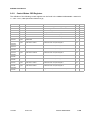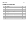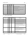
1
ALMA2e User Manual
IBM
ALMA2e
PCI/VME 2eSST Bridge
User Manual
User Manual
Version 1.0
2003
PreliminaryJune,7
Version
0.3
Dec 10, 2003
12/10/03
Version 0.3
-1
ALMA2e User Manual
IBM
About This Book
The objective of this user’s manual is to describe the functionality of the ALMA2e PCI/VME
Bridge for use by system designers and software developers.
Any published errata or updates to this document as well as Application Notes may be found at
web site:
http://www.chips.ibm.com/
Audience
This manual is intended for system software and hardware developers of VME products using
the industry-standard PCI Local Bus as the on-board local bus.
It is assumed that the reader has a knowledge of the IEEE-std-1014-1987 and VME64 versions
of the VMEbus Specification and of the PCI Local Bus Specification Revision 2.0.
References / Documentation
1. The VMEbus SPECIFICATION - conforms to ANSI/IEEE STD 1014-1987 - VITA
2. VME64 EXTENSIONS - ANSI/VITA 1.1 - 1997 - Oct 7,1998
3. VME 2eSST, VITA 1.5-200X/Draft 2.3 - Nov 6,2002
4. THE VMEbus SPECIFICATION - conforms to ANSI/IEEE STD 1014-1987 - VITA
5. THE VMEbus HANDBOOK - expanded third edition, Wade D. Paterson - VITA
6. PCI LOCAL BUS SPECIFICATION - Revision 2.2, December 18, 1998 - PCI SIG
7. PCI SYSTEM DESIGN GUIDE - Revision 1.0 8 September, 1993 - PCI SIG
Conventions
• “PCI Bus Specification” in the text refers to the “PCI Local Bus Specification, Revision 2.0”
• Active low signals are labelled with a “b” suffix, they are defined as true (asserted) when they
are at logic low (0).
• Active high signals are labelled with no suffix, they are defined as true (asserted) when they
are at logic high (1).
• Logic low on a signal corresponds to the low voltage, logic high to the high voltage.
Acronyms and Abbreviations
Msb:
BGA:
2eSST:
VMEbus:
SBC:
BLT:
MBLT:
-2
Most significant bit(s)
Ball Grid Array
two-edge Source-Synchroneous Transfer
VersaModule Eurocard bus
Single Board computer
Block Transfers
Multiplexed Block Transfers
12/10/03
ALMA2e User Manual
IBM
Table of contents:
Chapter 1. Overview . . . . . . . . . . . . . . . . . . . . . . . . . . . . . . . . . . . . . . . . . . . . . . . . . . . . .5
1.1 ALMA2e GENERAL DESCRIPTION . . . . . . . . . . . . . . . . . . . . . . . . . . . . . . . . . . . . . . . . . . . 5
1.2 Operating Specifications. . . . . . . . . . . . . . . . . . . . . . . . . . . . . . . . . . . . . . . . . . . . . . . . . . . . . 5
1.3 Features . . . . . . . . . . . . . . . . . . . . . . . . . . . . . . . . . . . . . . . . . . . . . . . . . . . . . . . . . . . . . . . . . 6
1.4 VMEbus signals external buffering example . . . . . . . . . . . . . . . . . . . . . . . . . . . . . . . . . . . . . 8
1.5 FUNCTIONAL DESCRIPTION . . . . . . . . . . . . . . . . . . . . . . . . . . . . . . . . . . . . . . . . . . . . . . . . 9
1.5.1 VMEbus interface . . . . . . . . . . . . . . . . . . . . . . . . . . . . . . . . . . . . . . . . . . . . . . . . . . . . . . 9
1.5.2 PCI bus interface . . . . . . . . . . . . . . . . . . . . . . . . . . . . . . . . . . . . . . . . . . . . . . . . . . . . . . 11
1.6 DMA . . . . . . . . . . . . . . . . . . . . . . . . . . . . . . . . . . . . . . . . . . . . . . . . . . . . . . . . . . . . . . . . . . . 13
1.7 Interrupt management . . . . . . . . . . . . . . . . . . . . . . . . . . . . . . . . . . . . . . . . . . . . . . . . . . . . . 13
1.8 Special Features. . . . . . . . . . . . . . . . . . . . . . . . . . . . . . . . . . . . . . . . . . . . . . . . . . . . . . . . . .
1.9 Addressing through the ALMA2e bridge. . . . . . . . . . . . . . . . . . . . . . . . . . . . . . . . . . . . . . . .
1.9.1 VME to PCI access . . . . . . . . . . . . . . . . . . . . . . . . . . . . . . . . . . . . . . . . . . . . . . . . . . . .
1.9.2 PCI to VME access (1K-Entry Mapping Table) . . . . . . . . . . . . . . . . . . . . . . . . . . . . . . .
14
15
15
16
1.10 Timings . . . . . . . . . . . . . . . . . . . . . . . . . . . . . . . . . . . . . . . . . . . . . . . . . . . . . . . . . . . . . . . .
1.10.1 Clock Timing . . . . . . . . . . . . . . . . . . . . . . . . . . . . . . . . . . . . . . . . . . . . . . . . . . . . . . . .
1.10.2 PCI IO Specifications. . . . . . . . . . . . . . . . . . . . . . . . . . . . . . . . . . . . . . . . . . . . . . . . . .
1.10.3 VME 2eSST Timings . . . . . . . . . . . . . . . . . . . . . . . . . . . . . . . . . . . . . . . . . . . . . . . . . .
18
18
18
19
1.11 REGISTER SET . . . . . . . . . . . . . . . . . . . . . . . . . . . . . . . . . . . . . . . . . . . . . . . . . . . . . . . . . 20
1.11.1 ALMA2e registers access mechanisms. . . . . . . . . . . . . . . . . . . . . . . . . . . . . . . . . . . . 20
1.11.2 ALMA2e Registers map. . . . . . . . . . . . . . . . . . . . . . . . . . . . . . . . . . . . . . . . . . . . . . . . 22
Chapter 2. ALMA2e REGISTERS . . . . . . . . . . . . . . . . . . . . . . . . . . . . . . . . . . . . . . . . . .23
2.0.1
2.0.2
2.0.3
2.0.4
2.0.5
2.0.6
2.0.7
2.0.8
2.0.9
PCI Configuration registers . . . . . . . . . . . . . . . . . . . . . . . . . . . . . . . . . . . . . . . . . . . . . . 25
PCI Operation registers . . . . . . . . . . . . . . . . . . . . . . . . . . . . . . . . . . . . . . . . . . . . . . . . . 35
ALMA2e Utility Registers. . . . . . . . . . . . . . . . . . . . . . . . . . . . . . . . . . . . . . . . . . . . . . . . 44
ALMA2e VME Registers . . . . . . . . . . . . . . . . . . . . . . . . . . . . . . . . . . . . . . . . . . . . . . . . 49
ALMA2E DMA Registers . . . . . . . . . . . . . . . . . . . . . . . . . . . . . . . . . . . . . . . . . . . . . . . . 61
ALMA2e Interrupt Operation Registers . . . . . . . . . . . . . . . . . . . . . . . . . . . . . . . . . . . . . 71
ALMA2e Extended Registers . . . . . . . . . . . . . . . . . . . . . . . . . . . . . . . . . . . . . . . . . . . . 81
Control/Status CSR Registers . . . . . . . . . . . . . . . . . . . . . . . . . . . . . . . . . . . . . . . . . . . 105
Configuration ROM (CR) Register. . . . . . . . . . . . . . . . . . . . . . . . . . . . . . . . . . . . . . . . 109
Chapter 3. SIGNAL DESCRIPTIONS . . . . . . . . . . . . . . . . . . . . . . . . . . . . . . . . . . . . . . .115
3.1 VME bus interface signals . . . . . . . . . . . . . . . . . . . . . . . . . . . . . . . . . . . . . . . . . . . . . . . . . 117
3.2 PCI bus interface signals . . . . . . . . . . . . . . . . . . . . . . . . . . . . . . . . . . . . . . . . . . . . . . . . . . 118
3.3 General purpose signals. . . . . . . . . . . . . . . . . . . . . . . . . . . . . . . . . . . . . . . . . . . . . . . . . . . 119
3.4 JTAG signals . . . . . . . . . . . . . . . . . . . . . . . . . . . . . . . . . . . . . . . . . . . . . . . . . . . . . . . . . . . 121
3.5 Manufacturing Test signal . . . . . . . . . . . . . . . . . . . . . . . . . . . . . . . . . . . . . . . . . . . . . . . . . 121
Chapter 4. PACKAGING . . . . . . . . . . . . . . . . . . . . . . . . . . . . . . . . . . . . . . . . . . . . . . . . .123
4.1 Ceramic BGA - 25mm - 361-pin - Package . . . . . . . . . . . . . . . . . . . . . . . . . . . . . . . . . . . . 124
Chapter 5. INITIALIZATION & RESET . . . . . . . . . . . . . . . . . . . . . . . . . . . . . . . . . . . . . .127
5.1 Overview. . . . . . . . . . . . . . . . . . . . . . . . . . . . . . . . . . . . . . . . . . . . . . . . . . . . . . . . . . . . . . . 127
12/10/03
Version 0.3
-3
ALMA2e User Manual
IBM
5.2 Reset with POWER_ON_RESETb . . . . . . . . . . . . . . . . . . . . . . . . . . . . . . . . . . . . . . . . . . . 128
5.3 Reset controlled by the RESETINb input . . . . . . . . . . . . . . . . . . . . . . . . . . . . . . . . . . . . . . 129
5.4 Reset controlled by the Addressed Reset operation . . . . . . . . . . . . . . . . . . . . . . . . . . . . . 130
5.5 Reset controlled by the V_SYSRESETib input (VME SYSRESET*) . . . . . . . . . . . . . . . . . 131
5.6 Reset controlled by the Reset Watchdog . . . . . . . . . . . . . . . . . . . . . . . . . . . . . . . . . . . . . . 131
5.7 Sampling hardware configurations . . . . . . . . . . . . . . . . . . . . . . . . . . . . . . . . . . . . . . . . . . . 131
5.8 Sampling VME System Controller pin. . . . . . . . . . . . . . . . . . . . . . . . . . . . . . . . . . . . . . . . . 131
5.9 Suggested usage of RESETINb and RESETOUTb pins . . . . . . . . . . . . . . . . . . . . . . . . . . 132
5.10 VME SYSFAIL* Handling . . . . . . . . . . . . . . . . . . . . . . . . . . . . . . . . . . . . . . . . . . . . . . . . . 132
5.11 Reset Watchdog . . . . . . . . . . . . . . . . . . . . . . . . . . . . . . . . . . . . . . . . . . . . . . . . . . . . . . . . 133
5.12 AUTO SLOT ID function . . . . . . . . . . . . . . . . . . . . . . . . . . . . . . . . . . . . . . . . . . . . . . . . . .
5.12.1 AUTO_SLOT_ID is at 1: . . . . . . . . . . . . . . . . . . . . . . . . . . . . . . . . . . . . . . . . . . . . . .
5.12.2 Normal AUTO_SLOT_ID operations: . . . . . . . . . . . . . . . . . . . . . . . . . . . . . . . . . . . .
5.12.3 input signal AUTO_SLOT_ID is at 0: . . . . . . . . . . . . . . . . . . . . . . . . . . . . . . . . . . . . .
134
134
134
135
Chapter 6. INTERRUPTS . . . . . . . . . . . . . . . . . . . . . . . . . . . . . . . . . . . . . . . . . . . . . . . .137
6.1 Interrupt Management overview . . . . . . . . . . . . . . . . . . . . . . . . . . . . . . . . . . . . . . . . . . . . .
6.2 Generating Interrupt to the VME from the PCI_AVITb pin . . . . . . . . . . . . . . . . . . . . . . . . .
6.2.1 «AVIT VME cycle». . . . . . . . . . . . . . . . . . . . . . . . . . . . . . . . . . . . . . . . . . . . . . . . . . . .
6.2.2 VME Interrupt Request Cycle (IRQ7-1*) . . . . . . . . . . . . . . . . . . . . . . . . . . . . . . . . . . .
137
138
138
138
6.3 Masking and Generating interrupts to the PCI . . . . . . . . . . . . . . . . . . . . . . . . . . . . . . . . . .
6.3.1 Routing to Interrupt Pin:. . . . . . . . . . . . . . . . . . . . . . . . . . . . . . . . . . . . . . . . . . . . . . . .
6.3.2 Routing to INT1b,2b,3b pins with CSR_USER_DEF_INT_MSKOUT . . . . . . . . . . . . .
6.4 Interrupt sources translated to an interrupt to PCI . . . . . . . . . . . . . . . . . . . . . . . . . . . . . . .
6.4.1 VME interrupts . . . . . . . . . . . . . . . . . . . . . . . . . . . . . . . . . . . . . . . . . . . . . . . . . . . . . . .
6.4.2 Addressed Interrupts . . . . . . . . . . . . . . . . . . . . . . . . . . . . . . . . . . . . . . . . . . . . . . . . . .
6.4.3 ALMA2e exceptions, end of DMA or timeout Interrupts . . . . . . . . . . . . . . . . . . . . . . .
139
140
141
142
142
142
143
6.5 VMEbus Interrupter. . . . . . . . . . . . . . . . . . . . . . . . . . . . . . . . . . . . . . . . . . . . . . . . . . . . . . . 144
6.5.1 ALMA2e VME interrupt generation through Register: . . . . . . . . . . . . . . . . . . . . . . . . . 144
6.6 ALMA2e response to a VME interrupt acknowledge cycle . . . . . . . . . . . . . . . . . . . . . . . . . 145
Chapter 7. ERROR HANDLING . . . . . . . . . . . . . . . . . . . . . . . . . . . . . . . . . . . . . . . . . . .146
Chapter 8. DMA Controller Operations . . . . . . . . . . . . . . . . . . . . . . . . . . . . . . . . . . . .147
8.1 Overview . . . . . . . . . . . . . . . . . . . . . . . . . . . . . . . . . . . . . . . . . . . . . . . . . . . . . . . . . . . . . . . 147
8.2 DMA Channels programming . . . . . . . . . . . . . . . . . . . . . . . . . . . . . . . . . . . . . . . . . . . . . . . 147
8.3 DMA Operation Timing . . . . . . . . . . . . . . . . . . . . . . . . . . . . . . . . . . . . . . . . . . . . . . . . . . . . 150
Chapter 9. ENDIAN CONVERSIONS . . . . . . . . . . . . . . . . . . . . . . . . . . . . . . . . . . . . . . .151
9.1 VME data Big Endian conversion to Little Endian . . . . . . . . . . . . . . . . . . . . . . . . . . . . . . . 151
9.2 PCI data Little Endian conversion to Big Endian . . . . . . . . . . . . . . . . . . . . . . . . . . . . . . . . 153
-4
12/10/03
ALMA2e User Manual
IBM
Chapter 1. Overview
1.1
ALMA2e GENERAL DESCRIPTION
ALMA2e provide an highly integrated single chip solution to interface a VME64 bus with 2eSST
protocol (two-edge Source-Synchroneous Transfer) and a 64-bit 66 Mhz PCI Bus.
All the bridge features are fully programmable from PCI bus or VME bus.
This component allows VMEbus single board computer and I/O board vendors to develop solutions
with PCI support, taking, thus, advantage of the growing family of PCI components in the market.
For VME backplanes applications with 2eSST protocol, the SN74VMEH22501 universal bus
transceivers is recommended.
ALMA2e is software compatible with the previous PCI to VME bridge called ALMA_V64, since it
covers all the ALMA_V64 functionality at the exception of the internal PCI arbitration that is no longer
implemented. Also the pinning has been changed to take into account more advanced CMOS
technology with a dual 2.5V, 3.3V power supply.
1.2
Operating Specifications
ALMA2e PCI to VME Bridge Specifications
Technology
0.25 um - IBM CMOS SA-12E
Temperature Range
-40 to 85 °C ambient (105 °C Junction)
Performance
Estimate
up to 70 MByte/sec on the VME64x
up to 256 MByte/sec on VME with 2eSST protocol
(340 MByte/sec peak)
up to 528 MByte/sec on the PCI 64 @ 66MHz
Signal I/Os
252
Power Supply
2.5V +/- 5% Core
3.3V +/- 5% I/Os (all I/Os are 5V tolerant)
Power Dissipation (est.)
0.9 W Worst case @ 66 Mhz Estimated
Packaging
25x25mm, Ceramic BGA 360-ball, 1.27mm pitch
12/10/03
Version 0.3
Overview
1-5
ALMA2e User Manual
1.3
IBM
Features
External
Interrupts
(4)
PCI Bus 64bit-66Mhz
A/D64
Interrupt
ALMA
from PCI
(1)
PCI Bus
Interrupt
Control.
Bus Request,
Bus Grant
PCI Bus
Requestor
PCI Bus
Interface
1K-entry
Mapping
Table
Registers
Resets
Timers,
Clocks
2-Channel
DMA
Controller
VME Data
FIFO
up to 2KB
PCI Data
FIFO
up to 2KB
JTAG
VME Bus VME Bus
System
Requestor
Control.
Utility
Bus
VME Bus
Interrupt
Controller
Data Transfer Priority Interrupt
Arbitration
Bus
Bus
VME Bus
Data Transfer
Interface
Data Transfer Bus
A64:D64
VMEbus 2eSST
Figure 1 : ALMA2e block diagram
High performance Bridge between PCI and VME
•
•
•
•
•
•
1-6
Asynchronous transfers between PCI and VME
Deep decoupling Transmit and Receive FIFOs
VME64 compliant, up to 70 MBytes/sec
External VME buffers, TTL and ETL buffers supported
Register set fully accessible from both the PCI bus and the VMEbus ports
Two-channel programmable DMA Controller
12/10/03
ALMA2e User Manual
IBM
VMEbus interface
•
•
•
•
•
•
•
•
•
•
•
•
•
•
VME64 and IEEE-std-1014-1987 compliant
VMEbus System Controller
Autoslot ID mechanism
VMEbus Requestor (Level 0-3)
VMEbus Interrupter and Interrupt handler (IRQ1-7)
VMEbus master/slave A32, A24, A16:D32, D16, D8, UAT
VMEbus master/slave A32, A24:D32BLT, D64MBLT
VMEbus master/slave A64, D32, D32BLT, D64MBLT
VMEbus master/slave 2eSST: A64, A32
VMEbus master/slave 2eSST Broadcast: A64, A32
Programmable VME slave image base address and size (16 VME slave channels) and
VME to PCI access conversion (address translation, bus cycles parameters).
Programmable Posted Write, Prefetch Read, coupled mode
BLT/MBLT cycle
Semaphore registers
PCI 64-bit 66MHz bus interface
•
•
•
•
•
Fully compliant, 64-bit, 25 to 66 MHz PCI bus interface Revision 2.2
PCI master/slave with burst operation
1K-entry on-chip Mapping Table for PCI to VME access conversion (address translation,
bus cycle parameters)
Little Endian / Big Endian byte ordering conversion with programmable conversion modes
Programmable Posted Write, Prefetch Read, coupled mode
Clocking
•
•
PCI clock : 25 to 66MHz
VME Clock : 64MHz
IEEE 1149.1 JTAG testability support
Available in high density 360-Ball BGA packages
Interfaces to both 3V and 5V technologies
12/10/03
Version 0.3
Overview
1-7
ALMA2e User Manual
1.4
IBM
VMEbus signals external buffering example
The following figure shows how external signal buffering can be done with either 74ABT, or ETL or
SN74VMEH22501 or equivalent technologies. ALMA2e control signals xxxDIR are used to set the
direction of the corresponding signals. For the Open collector type of drivers, it is possible to choose
between inverting and non inverting signal by placing a 1 or a 0 on the OC_CTL input pin of ALMA2e.
Possible Technology:
Buffer
V_D[31:0]
V_A[31:1]
V_LWORDb
OE
ADIR
A2B
A
V_IACKb
AMDIR
Vcc
OEb
DSDIR
ALMA2e
V_DSb[1:0]
Vcc
GND
ASDIR
V_ASb
Vcc
GND
SYSCONDIR
V_BCLRb
V_SYSCLK
(no R-pull-up
is required)
GND
SN74VMEH22501
B
Three-state 48 mA
OEb
OEb
V_AM[5:0]
V_WRITEb
A2B
A
x4
Three-state 48 mA
B
OE
A2B
A
Three-state 48 mA
B
x1
AM[5:0]
WRITE*
IACK*
DS1-0*
x1
Three-state 64 mA
B
OE
A2B
A
Three-state 64 mA
B
OE
A2B
A
A[31:1]
LWORD*
x4
OE
A2B
A
D[31:0]
AS*
VME BUS
DDIR
x1
Three-state 64 mA
B
OE
BCLR*
SYSCLK
x1
Vcc
DTACKDIR
V_DTACKb
GND
A2B
A
Three-state 64 mA
B
DTACK*
RETRY*
OE
x1
V_BR3-0o
V_SYSRESETo
V_RETRYo
V_BBSYo
V_IRQ7-1o
V_SYSFAILo
V_BERRo
x4
V_RETRYib
V_ACFAILib
V_BR3-0ib
V_SYSRESETib
V_BBSYib
V_SYSFAILib
V_BERRib
V_IRQ7-1ib
Open-Collector 48 mA
(option)
Y
GND
OE
A
x2
ACFAIL*
BR3-0*
SYSRESET*
SYSFAIL*
BBSY*
IRQ7-1*
BERR*
Figure 2 : VME buffering of ALMA2e signals
1-8
12/10/03
ALMA2e User Manual
1.5
IBM
FUNCTIONAL DESCRIPTION
The ALMA2e VME/PCI bridge is an highly flexible component that supports Master and Slave bus
operations on both the PCI bus and VMEbus ports.
1.5.1
VMEbus interface
• VME Master interface
The ALMA2e VME master module provides D32, D16, D8 and UAT under A32, A24 and A16
addressing modes plus D64 BLT and D32BLT under A64, A32 and A24 addressing modes. Any
Address Modifier (AM) is supported.
The VME block mode, D64 or D32, can be automatically started from a PCI burst. The use of internal
FIFOs allows maximum speed in decoupled mode (Read-ahead or Write-posting).
A set of registers allows users to set the new FIFO behavior with a high flexibility according to
different VME applications.
As a VME master in DMA mode ALMA2e provides A64, A32, broadcast A32 and broadcast A64
2eSST transaction. ALMA2e allows five different speed for 2eSST transfer. Data reception can be
done at the theoretical maximum speed of 320 Mb/sec.
• VME Slave interface
The ALMA2e VME slave interface supports the same addressing mode and data size as the VME
master interface.
Sixteen decoding channels are available for accessing the PCI bus from the VME bus. Each channel
can be configured independently in the A64, A32, A24, A16 address space.
Height out of 16 channels can be configured independently in the A64 2eSST, A32 2eSST, A64
2eSST broadcast or A32 2eSST broadcast address space.
These channels allow the user to program the PCI bus access parameters with a minimum
granularity of 1 Mbyte.
A set of registers allows users to set the new FIFO behavior with a high flexibility according to
different VME applications.
As Slave ALMA2e provides A64, A32, broadcast A32 and broadcast A64 2eSST transaction.
ALMA2e allows five different speed for 2eSST transfer. Data reception can be done at the theoretical
maximum speed of 320 Mb/sec.
VME RMW cycle is supported by ALMA2e, however the targeted PCI resource is not locked during
the read and write (ALMA2e does not support the PCI LOCK mechanism).
Each channel can be configured with selectable parameters. An additional channel available under
A16 or A24 CR/CSR space is provided for ALMA2e internal registers access.
ALMA2e provides an A24 CR/CSR space as define in the VME64x specification.
12/10/03
Version 0.3
Overview
1-9
ALMA2e User Manual
IBM
• VME bus requester
ALMA2e drives the bus requests on the 4 levels, BR0 to BR3 (optional FAIR policy), and the release
of the bus can be managed with ROR (Release On Request), RWD (Release When Done), ROC
(Release On Clear) or RNE (Release NEver) policy.
• VME System controller
ALMA2e is VME bus system controller if the input pin VME_SYSCONT_INb is strapped to Ground.
ALMA2e supports the «auto system controller» mechanism as defined into the VME64 norm, if this
pin is connected to the VME BG3IN* signal and if the backplane interface logic on board connects a
3-Kohm resistor between BG3IN* and the ground.
ALMA2e includes a mechanism for VME64x AUTO SLOT ID operation.
The following modules are activated if ALMA2e is selected as the VME system controller:
-
-
VME arbiter with two arbitration capabilities: PRI (fixed priority), RRS (Round Robin)
depending on the user choice. A fixed arbitration time-out of 8ms is selectable between
BGOUT* transmission and BBSY* reception.
DTB Timer. A programmable timer (4 us to 256 us) measures the elapsed time between
the DS* assertion and the DTACK* or BERR* signal.
SYSCLOCK generator at 16 MHz.
SYSRESET* can be generated (See Special Features).
SYSFAIL* generator, from specific pin SYSFAILINb or from a special ALMA2e register
access.
Operation in 2eSST mode
ALMA2e supports 2eSST transfers as defined in the Vita 1.5 standard. As a VME slave, up to 8
addressing windows can be programmed to accept 2eSST transfers. ALMA2e will initiate 2eSST
transfers over the VME by a dedicated setting of the internal DMA controller.
No 2eSST transfers will be generate over the VME as a result of a PCI slave operation. Only the 6U
version of the standard is implemented. The slower 2eVME protocol is not supported.
During address phase 1 (the first DS0* assertion), an address modifier encoding of 0x20 is used for
2eSST transfers. The extended AM codes used by ALMA2e as a VME master or slave are shown in
table 1 below:
TABLE 0.1
Extended Address Modifier codes
0x11
0x12
0x21
0x22
Extended AM for 2eSST used by ALMA2e
Address/Data Mode
A32/D64 2eSST
A64/D64 2eSST
A32/D64, Broadcast 2eSST
A64/D64, Broadcast 2eSST
Address phase 2 (DS0* de-assertion) includes the cycle count and the speed rate. For the
cycle count, ALMA2e uses either the block size programmed in the DMA controller (divided by two
because of the 2 edges) or a smaller value to avoid crossing a 2 KB boundary or to avoid transferring
more data than requested at the end of the DMA.
1-10
12/10/03
ALMA2e User Manual
IBM
As a 2eSST data receiver, ALMA2e can accept all the possible rates: SST160, SST267, SST320.
However, depending on particular system timing performance behavior, it is possible not to accept
transfers at SST320 rate by clearing bit 3 of VME2ESST_CTL register; a slave error would then be
generated during address phase 3 if a rate of SST320 was detected by ALMA2e as a slave.
As a 2eSST data source, ALMA2e generates one of the 3 possible rate codes (SST160, SST267,
SST320) according to its DMA_CHN_RATE register setting. The actual timings of the 2eSST are
based on the setting of register VME2ESST_CTL. It is the user responsibility to program actual
2eSST timings compatible with the 2eSST rate code selected: actual timings should correspond to a
rate less than or equal to the rate code, with set-up and hold times greater than or equal to the 2eSST
requirements.
During address phase 3 (DS0* reassertion), if a broadcast 2eSST operation has been selected
(XAM 0x21 or 0x22), VME addresses A21 to A1 indicate the geographical address of the slaves to be
targeted by the broadcast. To select a slave with a geographical address i, bit Ai should be set to 1.
For each DMA channel, the slaves participating in the broadcast operation are programmed in
register DMA_VME_SLVSEL.
During the broadcast operation, the master responds with DTACK* to its own cycles, and the
participating slaves capture the transmitted data. If a slave is not ready to accept the full broadcast
operation, it asserts RETRY* during address phase 3 to request for the transfer to be restarted.
1.5.2
PCI bus interface
• PCI Bus command
ALMA2e initiates and responds to a subset of PCI bus commands. PCI bus command is defined by
the P_CBELb[3:0] signals during the address phase of a transaction. The Table 1 defines the PCI bus
command subset that the ALMA2e supports as a slave and as a master.
TABLE 0.2
P_CBELb[3:0]
12/10/03
PCI Commands supported by ALMA2e
Command Type
Supported as Slave
Interrupt acknowledge
0001
Special Cycle
No
Yes
0010
IO read
Yes
Yes
0011
IO write
Yes
Yes
0100
Reserved
No
Yes
0101
Reserved
No
Yes
0110
Memory Read
Yes
Yes
0111
Memory Write
Yes
Yes
1000
Reserved
No
Yes
1001
Reserved
No
Yes
1010
Configuration Read
Type 0 : Yes
Type 1 : No
Type 0 : Yes
Type 1 : Yes
1011
Configuration Write
Type 0 : Yes
Type 1 : No
Type 0 : Yes
Type 1 : Yes
1100
Memory Read multiple
Yes: Aliased to Memory Read
Yes
1101
Dual Address cycle
No
No
1110
Memory Read Line
Yes: Aliased to Memory Read
Yes
1111
Memory Write & Invalidate
Yes: Aliased to Memory Write
Yes
Version 0.3
No
Supported as Master
0000
Yes
Overview
1-11
ALMA2e User Manual
IBM
• PCI Master Interface
The ALMA2e PCI master interface can generate I/O cycle, all the MEMORY cycles, Interrupt
Acknowledge, Special cycle and Type 0 and 1 Configuration cycles.
Interrupt Acknowledge or Special Cycle can be initiated from the VME through a read or write access
to a specific ALMA2e internal register.
Configuration cycles for primary and secondary buses can be initiated from the VME through access
to two specific ALMA2e internal registers used as configuration address and configuration data
registers, according to mechanism #2 of the PCI specification.
ALMA2e can generate PCI burst up to 2KB without wait state.
• PCI Slave interface
The ALMA2e PCI slave interface decodes I/O cycles, MEMORY cycles and Type 0
CONFIGURATION cycles.
Note that MEMORY READ MULTIPLE, MEMORY READ LINE and MEMORY WRITE & INVALIDATE
are also accepted by ALMA2e but are treated as regular MEMORY READ or MEMORY WRITE
accesses.
ALMA2e slave image base addresses and address spaces are encoded into 6 PCI Base Address
Registers defined into its Configuration Header space.
Five Base Address registers (BAR) are available for decoding of PCI accesses to the VME and one
Base Address register is reserved for decoding of PCI I/O accesses to ALMA2e Configuration space
registers.
PCI to VME address translation through 1K Mapping table
In addition a Mapping table of 1K entries is used to enable/disable PCI MEMORY space accesses (up
to 4GB) as well as PCI I/O space accesses (up to 4GB), with a granularity of 8MB. For a given 8MB
addresses block, ALMA2e selects the associated Mapping Table entry in which are programed: the
VAL bit to enable/disable the PCI access, the WP bit to enable/disable PCI Write Posting, plus all the
parameters required to generate a master access onto the VMEbus, such as: address bits for PCI to
VME address translation (ADD, 9 bits), the VME Address Modifiers (AM, 6 bits), Little/Big Endian
conversion mode (LEBE coded on 2bits), and Read-Ahead enable (RA, 1bit).
To accommodate software mapping flexibility requirements, ALMA2e allows for some programming of
its slave image characteristics via a selectable feature. So, the so-called hard-coded recognition
address range depth and space (as defined by the base address field size and the I/O
space/MEMORY space indicator bit value within the PCI Base Address Register layout) can be
selectively overridden by programmed values.
As slave ALMA2e can receive PCI burst up to 2KB without wait states during data phase.
1-12
12/10/03
ALMA2e User Manual
1.6
IBM
DMA
ALMA2e has two DMA channels, user accessible, with a programmable priority between channels,
and the option that blocks from the two channels may be interleaved.
Each channel is initialized with a source address, a destination address, a transfer count up to 16
MBytes (2M words of 64 bits maximum), a block count up to 2KBytes (up to 256 words of 64 bits),
plus all the necessary control data (VME Address Modifiers, PCI bus command, transfer direction,
etc.).
When DMA ends, the information related to the completion of the DMA (normal ending or a
description of the errors) is available in an interrupt status register and an error status register. DMA
completion can be signalled via an interrupt to the PCI bus.
The DMA engine supports all of the 2eSST operations (A64, A32, A64 broadcast and A32 broadcast
transaction). ALMA2e allows five different speed for 2eSST transfer. Data reception can be done at
the theoretical maximum speed of 320 Mb/sec.
Table 1: DMA performance
Transaction Type
DMA PCI to VME Single
DMA PCI to VME BLT D32
DMA PCI to VME MBLT D64
DMA PCI to VME 2eSST mode
DMA VME to PCI Single
DMA VME to PCI BLT D32
DMA VME to PCI MBLT D64
DMA VME to PCI 2eSST mode
1.7
Performance MB/sec
8
34
70
240
7
22
50
230
Interrupt management
The ALMA2e interrupt controller can handle different interrupt sources:
-
7 VME interrupts (IRQ7*-IRQ1*).
8 addressed interrupts (occur when a specific 8-bit register is addressed in write mode
from the PCI or the VME).
ACFAIL* and SYSFAIL* on VMEbus.
Internal Exceptions (End of DMA, error acknowledges on PCI bus or VMEbus, VMEbus
arbitration time-out...).
All these interrupts can be masked and can drive either the PCI bus interrupt pin (P_INTAb) or 3
additional programmable interrupt pins: P_INT1b, P_INT2b or P_INT3b.
ALMA2e can also generate VME Interrupts (IRQ7*-IRQ1*) when a specific 8-bit register is addressed
in write mode from the VMEbus or the PCI bus. The release mechanism of this interrupter is ROAK
(Release on Acknowledge).
An external interrupt input pin (PCI_AVITb) allows also to generate either VME interrupts (IRQ7*IRQ1*) or a VME bus cycle whose characteristics are fully programmable (read or write cycle, value
of address, address modifiers and data).
12/10/03
Version 0.3
Overview
1-13
ALMA2e User Manual
1.8
IBM
Special Features
• Reset controller
ALMA2e handles the following Reset sources:
-
Power-on-reset when input pin POWER_ON_RESETb is asserted Low.
VME reset (SYSRESET*) when input pin V_SYSRESETib is asserted Low.
Local reset when input pin RESETINb is asserted Low.
Addressed Reset when a specific 8-bit register is addressed in write mode.
Reset due to Reset Watchdog function.
These resets can be propagated to the locations below according to programming:
-
ALMA2e internal reset
VME reset (SYSRESET*): assertion of the V_SYSRESETo pin High.
Local reset: assertion of the RESETOUTb pin Low.
• Data conversion
Little Endian and Big Endian byte ordering conventions are fully supported by ALMA2e. Little
Endian/Big Endian conversions are automatically performed on both data directions, according to a
programmable conversion mode as defined below (refer to the LEBE field of the VME slave channels
and of the PCI Mapping Table entry):
- LEBE=00: “No conversion“ ( Data byte ordering and Address 2 low-order bits remain unchanged)
- LEBE=01: “Address Coherency“
(Data bytes are swapped, Address 2 low-order bits remain unchanged)
- LEBE=10: “Data Coherency”
(Data byte ordering remain unchanged, Address 2 low-order bits are modified)
- LEBE=11: “Bytes Translation with No Swapping”
(Data bytes are translated, Address 2 low-order bits remain unchanged)
• Hardware semaphores
VME Multiprocessor architectures often need to be able to share common resources between
different VME cards. The ability for a card to have hardware mechanisms for handling semaphores is
therefore necessary.
The standard VME rev C Read-Modify-Write cycle is able to support semaphores. Unfortunately,
there are a few drawbacks in using this RMW VME protocol:
• VME rev C RMW is a slow mechanism and its support can even slow down non RMW standard
cycles. This is due to the signalling method on the VME: indeed, indivisible cycles can only be
recognized at the end of the read phase.
• RMW cycles are often not used nor generated by modern microprocessor architectures, and
hardware emulation of such cycles is not easy to design.
For these reasons, the ALMA2e chip includes 4 shared 8-bit Semaphore registers so that the design
of VME multiprocessor architectures can be greatly simplified.
1-14
12/10/03
ALMA2e User Manual
IBM
• VMEbus DeadLock avoidance Feature:
BRLOCb & BGLOCb pins / VME_REQ_LBR & VME_REQ_LBG bits
In order to prevent deadlock situations, ALMA2e is providing a mechanism allowing a PCI bus master
device to obtain the VMEbus ownership before it starts its access to ALMA2e. By doing so, the device
is guaranteed that ALMA2e will not retry its transaction. This feature can be advantageously used by
those PCI bus master devices which are not supporting the PCI Retry protocol and which therefore
may be responsible of deadlocks.
The mechanism has two implementations, one is under pin control (BRLOCb as bus request pin,
BGLOCb as bus grant pin) the other is under software control through the “VME Request control
register” at the address @70. The bit VME_REQ_LBR of this register is used for bus request, and the
bit VME_REQ_LBG for bus grant.
Once granted the PCI master device issues transaction to access VME resources as long as it
wishes, and must hold the BRLOCb pin active during all the time it is operating. However, ALMA2e
may at any time ask the device to release the VMEbus by de-asserting BGLOCb or resetting the
VME_REQ_LBG bit (this event may also be signalled via an interrupt). In this case the device must
stop its current transaction as soon as it can and signal that it has finished its operation by deasserting the BRLOCb pin or by resetting the VME_REQ_LBR bit.
1.9
Addressing through the ALMA2e bridge
High Addressing flexibility is a key feature to enable a bridge such as ALMA2e to accommodate a
whole range of uses, from a simple SBC (Single Board Computer) VME card to a complex VME
multiprocessor architecture: in the majority of VME computer designs, software compatibility (at user
and kernel level) with existing standard desktop workstations or PCs is a major issue and ALMA2e
addressing flexibility allows the VME computer to use the same address mapping convention as the
one defined by the chosen microprocessor architecture.
1.9.1
VME to PCI access
As a VME Slave, ALMA2e decodes if its VME slave image address and address modifiers are the
target of the VME access, through use of 16 decoding channels whose address recognition range
depth is programmable (1MB to 4GB Min/Max depth). These features accommodate well with the big
parcelling out of the VME address map sometimes found in VME systems.
To permit the mixing of VME64 and 2eSST, 8 out of 16 Channels can be programmed as 2eSST.
ALMA2e responds to the VME access under the following conditions:
- VME address 12 Msb match the address field of at least one channel.
- VME address modifiers match the address modifiers field of the channel that has been hit.
- The channel that has been hit is enabled.
A prioritization is performed between channels when more than one is hit. The PCI address is
obtained through a translation of the VME address with a granularity of 64KB. Thus, the offset field of
the selected channel is added to the 16 Msb of the VME address. While the PCI bus command is
obtained from the PCI bus command field of the selected channel
These capabilities allows for high mapping flexibility of VME addresses into the 4GB PCI address
MEMORY and I/O spaces.
12/10/03
Version 0.3
Overview
1-15
ALMA2e User Manual
IBM
VME address
31
20
VME address modifiers
15
0
5
0
(3) (3)
3/8 encode
=
3/8 encode
=
&
&
Enable bit
ALMA2e
VME
target hit
chn15
16 VME
channels
chn0 ADD(12) ADDMSK(12)
VME address
E(1)
AM(16)
31
chn15
chn0
16 15
1
(3) (2) (1) (1)
OFFSET(16)
WP0ST: Write Posting
enable
RAHEAD: Read Ahead
enable
LEBE: Little/Big Endian
conversion mode
0
16 (64KB)
Add
Generated PCI address
31
16
15
Generated PCI
command
0
3 1 0
BUSCOM: PCI bus command
r/w
Figure 3 : VME slave decode & address translation mechanisms for a VME access to PCI.
1.9.2
PCI to VME access (1K-Entry Mapping Table)
ALMA2e as a PCI slave implements 6 Base Address Registers for PCI bus address and command
decode.
At Reset these registers are initialized such as to define five ranges of 256 MB mapped in the MEMORY
space (3 ranges) and in the I/O space (2 ranges) while one range of 256B mapped in the I/O space has
been reserved for decoding of those PCI I/O cycle accessing internal registers.
After reset, the five 256MB windows can be changed to any size from 16MB up to 2GB and to any space
(I/O or MEMORY) thru registers programming. Besides the regular decode through Base Address
Registers, an additional validation of the PCI access is performed with a granularity of 8MB in the
MEMORY or I/O space. For that purpose ALMA2e implements a 1K-entry programmable Mapping Table,
whose low-order 512-entries are used to validate MEMORY accesses while the high-order 512-entries are
used to validate I/O accesses (through a validation bit, VAL, programmed in the entry line). PCI address
9Msb are used to index one or the other of these blocks, according as PCI cycle is MEMORY or I/O.
1-16
12/10/03
ALMA2e User Manual
IBM
n# 6
n# 2
31
PCI Base Address Registers
28
0
24
space indicator
4
=
&
base address
(1 to 8 bits
can be selected)
PCI address
1 0
Dec
1
ALMA2e
PCI
target hit
4 MSb (from 1 MSb up to 8 MSb can be selected)
PCI command
3
&
=
23
31
index 9
LSbits
index
MSbit
=0 : MEMORY cycle
=1 : I/O cycle
0
1023
index
10 bits
1K-entry PCI to VME
Mapping Table
0
ADD(9)
Address bits
for translation
LEBE:
AM (6) (2) (1) (1) (1)
VME
Address
Modifiers
Little/Big Endian
conversion mode
5
0
VME AM
RA:
WP:
VAL:
31
23
0
Generated VME Address
Read-Ahead enable
Write Posting enable
PCI MEMORY access Valid (for indexes=0-511)
PCI I/O access Valid (for indexes=512-1023)
Thus, ALMA2e selects itself as the target of the PCI access when both Base Address Registers and
Mapping Table are hit.
The selected Mapping Table entry tells the ALMA2e PCI slave behavior on writes (write posting
enable/disable) and provides all the informations useful to cycle generation onto the VMEbus, such as
address translation, address modifiers, Little Endian/Big Endian conversion mode and read prefetch
enable/disable
The Mapping Table can be disabled through programming. In that mode, called «transparent mode», an
ALMA2e register content and some hard-coded informations substitutes themselves to the Mapping Table
programming.
The register provides two informations:
- The first indicates whether PCI access can be accepted or rejected (no distinction is made between
MEMORY or I/O space accesses and the 8MB granularity does not apply anymore),
- The second provides address modifiers value of the VME cycle to generate.
All others informations are hard-coded as follows:
no address translation (PCI address is forwarded as is onto the VMEbus), Little Endian/Big Endian
conversion mode set to the Address Coherency mode, read prefetching and write posting set to disabled.
12/10/03
Version 0.3
Overview
1-17
ALMA2e User Manual
IBM
1.10 Timings
1.10.1 Clock Timing
Table 2: Clock timing
Parameter
Min
Typical
Max
Units
VME_CLK input frequency
-
64
-
MHz
VME_CLK duty cycle
40
60
%
P_CLK
25
66
Mhz
P_CLK duty cycle
40
60
%
1.10.2 PCI IO Specifications
Following timing are given for ALMA2e as input or output on a PCI bus at 66 MHz, loaded by 10 pF.
Worst Case conditions : 105 degrees junction temperature
and voltage -5%
Best Case conditions : -40 degrees junction temperature
and voltage +5%
Table 3: PCI timing
PCI Signal
1-18
Input
Output
Setup (min)
Hold (min)
Min
Max
P_ADL[31:0]
3.00 ns
0 ns
2 ns
6 ns
P_ADH[31:0]
3.00 ns
0 ns
2 ns
6 ns
P_CBELb[3:0]
3.08 ns
0 ns
2 ns
6 ns
P_CBEHb[3:0]
3.00 ns
0.09 ns
2 ns
6 ns
P_FRAMEb
3.34 ns
0.06 ns
2 ns
6 ns
P_REQ64b
3.00 ns
0 ns
2 ns
6 ns
P_IRDYb
3.37 ns
0.12 ns
2 ns
6 ns
P_DEVSELb
3.19 ns
0.19 ns
2 ns
6 ns
P_ACK64b
3.21 ns
0 ns
2 ns
6 ns
P_TRDYb
3.13 ns
0.08 ns
2 ns
6 ns
P_STOPb
3.10 ns
0.22 ns
2 ns
6 ns
P_PAR
3.00 ns
0 ns
2 ns
6 ns
P_PAR64
3.00 ns
0ns
2 ns
6 ns
12/10/03
ALMA2e User Manual
IBM
1.10.3 VME 2eSST Timings
Following timings are given for ALMA2e in 2eSST mode.
For the Set up/ Hold timings of the ALMA2e DATA as input, the reference signal is DS1 in Write and
DTACK in Read.
Note that the 2eSST specifies the timings at the Back plane connector.
Table 4: VME2eSST timing
Effective
transfer rate
Speed selection
VME2ESST_CTL[8:12]
Setup/Hold
at source
ALMA2
VME 2eSST Code
((VITA 1.5 setup/hold
at source connector)
number of VME_CLK
(64 MHz or 60 MHz)
146 MBytes/s
VERY_SLOW
(0x01)
23.4 ns
3.5 VME_CLK
(54,6 ns @ 64 MHz)
SST 160 ( 18 ns )
171 MBytes/s
SLOW
(0x02)
15.6 ns
3 VME_CLK
(46.8 ns @ 64 MHz)
SST 267 (10.8 ns)
205 MBytes/s
MEDIUM
(0x04)
15.6 ns
2.5 VME_CLK
(39.0 ns @ 64 MHz)
SST 267 (10.8 ns)
256 MBytes/s
FAST
(0x08)
15.6 ns
2 VME_CLK
(31,2 ns @ 64 MHz)
SST 267 (10.8 ns)
341 MBytes/s
ULTRA_FAST
(0x10)
7.8 ns
1.5 VME_CLK
(23,4 ns @ 64 MHz)
SST 320+
320 MBytes/s
ULTRA_FAST
(0x10)
8.35 ns
1.5 VME_CLK
(25.0 ns @ 60 MHz)
SST 320 (9 ns)
12/10/03
Version 0.3
Overview
1-19
ALMA2e User Manual
IBM
1.11 REGISTER SET
1.11.1 ALMA2e registers access mechanisms
1- ALMA2e registers Space:
ALMA2e Configuration Space
A space named «ALMA2e Configuration Space» of 256 entries (Bytes) is allocated to internal
registers. All the internal registers are intrinsically in the little-endian byte ordering convention. In the
following register description, bit 0 is the least significant bit of the register.
It is composed of the «ALMA2e Configuration Space Header» for address offsets ranging from 0x00
to 0x3F, and of the «ALMA2e Configuration Space Specific» for address offsets ranging from 0x40 to
0xFF.
A VME master may access both spaces via VME A16 read/write cycles.
A PCI master may access both spaces via PCI CONFIGURATION cycles, and, access only the
«ALMA2e Configuration Space Specific» via PCI I/O cycles (this feature allows some PCI agents,
with no means to generate PCI CONFIGURATION cycles, to access ALMA2e configuration registers
too).
ALMA2e Extended Register Space
A second register space called “Extended Register Space” provides access to all of the new registers
(CR/CSR registers, transaction flexibility registers,...)
ALMA2e CR-CSR (Configuration ROM-Control Status) Register Space
This 512 KB register space is defined with a 8 0000 offset for PCI access.
x’00
Offset
PCI Configuration Header Registers
x’40
ALMA2e
Configuration
Space
(256 Registers)
PCI Operation Registers(*)
x’64
Utility Operation Registers
x’70
VME Operation Registers(*)
x’C0
DMA Operation Registers
x’E0
Interrupt Operation Registers
ALMA2e Extended
Register Space
x’FC
x’100
x’1FC
Figure 1-1. ALMA2e Configuration space and Extended Space Register
1-20
12/10/03
ALMA2e User Manual
IBM
2 - Access to internal ALMA2e’s registers
ALMA2e Identifying on VME Access to internal registers
On a VME A16 cycle, ALMA2e identifies its internal registers of the configuration space are accessed
when it decodes its VME Slave channel A address (VME_SLVA register) as the target of that access.
All of the internal register set is accessible from VME bus via A24 CR/CSR transaction.
ALMA2e Identifying on PCI Access to internal registers
ALMA2e will respond to a PCI CONFIGURATION cycle ALMA2e is when its P_IDSEL input pin is
asserted high.
ALMA2e identifies its internal registers are accessed via a PCI I/O cycle when it decodes its PCI Base
Address Register no 1 (PCIH_BA1 register) as the target of the access.
Access to Reserved registers
When PCI or VME access are performed on an internal «Reserved» register, except otherwise noted,
ALMA2e returns a value 0 on a Read, or takes no action (external common behavior) on a write.
3 - Accessing the Mapping Table
The 1K-entry PCI Mapping Table can be accessed via the 2 following internal registers:
-
Mapping Table index (PCI_RAM_INDEX register): counter which contains a Mapping
Table entry address
Mapping Table data (PCI_RAM_DATA register) virtual register: a write (or read) access
to that register address will make ALMA2e to load the write data (or to return content) at
Mapping Table offset pointed by the PCI_RAM_INDEX register.
To access the Mapping table, first the PCI_RAM_INDEX counter is loaded with a given starting offset,
then, any subsequent write (or read) access to the PCI_RAM_DATA register address will
automatically increment the counter. Current value of Mapping Table offset can be known at any time,
by reading PCI_RAM_INDEX register.
12/10/03
Version 0.3
Overview
1-21
ALMA2e User Manual
IBM
1.11.2 ALMA2e Registers map
The following diagram shows the ALMA2e’s register addressing organization. For compatibility with
previous product, and because the 512KB CR-CSR (Configuration ROM - Control/Status Register)
space starts at zero from the VME side, the ALMA2e Configuration space and ALMA2e Extended
space are accessed with 2 different addresses from the PCI
ALMA2e
Config Space
(256 Regs)
ALMA2e
Extended
00
00
CR
Configuration ROM
FF
100
8 0FFF
User CR Space
CR - CSR 512KB
CR
Configuration ROM
(offset = 8 0000)
00
FF
FFF
1FC
8 0000
ALMA2e
Config Space
(256 Regs)
User CR Space
BEG_USER_CR
END_USER_CR
Config RAM Unused BEG_CRAM
END_CRAM
BEG_USER_CSR
ALMA2e Config
Space (256 Regs)
ALMA2e
Extended
User
CSR
END_USER_CSR
7FC00
Config RAM Unused
CSR
Reserved
User CSR Space:
VME64 defined CSR
VME64x defined CSR
ALMA2e Config
Space (256 Regs)
7FF5F
7FFF3
7FFFF
ALMA2e
Extend
FFC00
CSR
Reserved
VME64 defined CSR
VME64x defined CSR
From PCI
IO Space
F FFFF
From VME
A24
From VME
A16
Figure 4 : ALMA2e Addressing Model.
1-22
12/10/03
ALMA2e User Manual
IBM
Chapter 2. ALMA2e REGISTERS
#
Register space
1
PCI Configuration registers
25
x’00 - 3C
2
PCI Operation registers
35
x’40 - 63
3
ALMA2e Utility Registers
44
x’64 - 6F
4
ALMA2e VME Registers
49
x’48 - BF
5
ALMA2e DMA Registers
61
x’C0 - DF
6
ALMA2e Interrupt Registers
71
x’E0 - FF
7
ALMA2e Extended Registers
81
x’100 - 1FC
8
CSR (Control Status Registers)
105
x’7FF5F - 7FFFF
9
CR (Configuration ROM) Registers
109
x’03 - FFF
12/10/03
Page
Version 0.3
Address Offset
ALMA2e REGISTERS
2-23
ALMA2e User Manual
2-24
IBM
12/10/03
ALMA2e User Manual
2.0.1
IBM
PCI Configuration registers
These registers are, from the PCI interface, only accessible in CONFIG mode access.
Address
Size
Name
Use
Page
0x00
2 bytes
PCIH_VID
Vendor ID register
26
0x02
2 bytes
PCIH_DID
Device ID register
26
0x04
2 bytes
PCIH_CMD
PCI Command register
27
0x06
2 bytes
PCIH_DSTAT
PCI Status register
28
0x08
1 byte
PCIH_REVID
Revision ID register
29
29
0x09
3 bytes
PCIH_CLSCD
PCI Class code register:
Register-level programming interface - 0x9
Sub-Class code - offset 0xA
Base class code - offset 0xB
0x0C
1 byte
PCIH_CLS
Reserved
29
0x0D
1 byte
PCIH_LT
PCI Latency timer register
29
0x0E
1 byte
PCIH_HT
PCI Header type register
30
0x0F
1 byte
PCIH_BIST
Reserved
0x10
4 bytes
PCIH_BA1_SPACE
PCI Base Address register no1
31
0x14
4 bytes
PCIH_BA2_SPACE
PCI Base Address register no 2
31
0x18
4 bytes
PCIH_BA3_SPACE
PCI Base Address register no 3
31
0x1C
4 bytes
PCIH_BA4_SPACE
PCI Base Address register no 4
31
0x20
4 bytes
PCIH_BA5_SPACE
PCI Base Address register no 5
31
0x24
4 bytes
PCIH_BA6_SPACE
PCI Base Address register no 6
31
0x28
4 bytes
Reserved
Reserved
0x2C
4 bytes
Reserved
Reserved
0x30
4 bytes
Reserved
Reserved
0x34
4 bytes
Reserved
Reserved
0x38
4 bytes
Reserved
Reserved
0x3C
1 byte
PCIH_ITLINE
PCI Interrupt line register
33
0x3D
1 byte
PCIH_ITPIN
PCI Interrupt pin register
33
0x3E
1 byte
PCIH_MINGNT
PCI Minimum grant register
34
0x3F
1 byte
PCIH_MAXLT
PCI Maximum latency register
34
12/10/03
Version 0.3
ALMA2e REGISTERS
Notes
2-25
ALMA2e User Manual
IBM
PCIH_VID
PCI Vendor ID register
Address from PCI interface:
Config space: 0x00
Address from VME interface:
IO space: not seen, access ends with Master Abort termination
A16 space: VME_SLVA + 0x00
A24 space: CR_CSR_BAR + BEG_USER_CSR + 0x00
Width:
16
Reset Value:
Access type:
0x1014
Read Only
PCIH_VID
15 14 13 12 11 10
9
8
7
6
5
4
3
2
1
Bit(s)
15 - 0
0
Description
Vendor Identification Number
Value 0x1014 (index 0x00 = 0x14, index 0x01 = 0x10)
PCIH_DID
PCI Device ID register
Address from PCI interface:
Config space: 0x02
Address from VME interface:
IO space: not seen, access ends with Master Abort termination
A16 space: VME_SLVA + 0x02
A24 space: CR_CSR_BAR + BEG_USER_CSR + 0x02
Width:
16
Reset Value:
Access type:
0x0035
Read Only
PCIH_DID
15 14 13 12 11 10 9
Bit(s)
15 - 0
2-26
8
7
6
5
4
3
2
1
0
Description
Device Identification Number
Value 0x0035
(index 0x02 = 0x35, index 0x03 = 0x00)
12/10/03
ALMA2e User Manual
IBM
PCIH_CMD
PCI Command register
Address from PCI interface:
Config space: 0x04
Address from VME interface:
IO space: not seen, access ends with Master Abort termination
A16 space: VME_SLVA + 0x04
A24 space: CR_CSR_BAR + BEG_USER_CSR + 0x04
Width:
16
Reset Value:
Access type:
Recommended value:
0x0000
Read/Write
0x0007
15 14 13 12 11 10
9
8
7
6
5
4
3
2
1
0
Bit(s)
Description
0
Enable PCI Slave IO space
set to 0
ALMA2e PCI IO access are Disable
set to 1
ALMA2e PCI IO access are Enable
1
Enable PCI Slave MEM space
set to 0
ALMA2e PCI MEM access are Disable
set to 1
ALMA2e PCI MEM access are Enable
2
PCI Master Enable
set to 0
ALMA2e will never generate PCI access as a Master
set to 1
ALMA2e may generate PCI access as a Master
3
Enable Special Cycle operation
Read only set to 0, ALMA2e never monitor Special Cycle as a slave.
Although this bit is set to 0, ALMA2e is able to generate PCI Special Cycles.
4
Enable Memory Write & Invalidate operation
Read only register set to 0.
Although this bit is set to 0, ALMA2e is able to generate and decode PCI Memory Write & Invalidate Cycles.
5
VGA Palette Snoop
Read only register set to 0. ALMA2e is not a VGA device.
6
Enable Parity Error Response
set to 0
ALMA2e masks detection of parity errors and P_PERRb is not asserted, although
parity is still generated.
set to 1
ALMA2e PCI bus parity errors detection is enable for all types of PCI transaction,
including the following:
PCI address bus parity errors
PCI data bus parity errors while PCI master
PCI data bus parity errors while PCI target
7
Address Stepping Control
Read only register set to 0. ALMA2e does not support address stepping as a PCI master nor as a PCI target.
8
P_SERRb Enable.
set to 0
ALMA2e never drives P_SERRb signal
set to 1
Enable the assertion of P_SERRb when a PCI parity error is detected.
The bit 6 (above) of the PCI command register must also be enable for parity error reporting.
9
Fast back to back enable.
Read Only set to 0, ALMA2e is not able to generate fast back to back transaction.
15-10
Reserved, These bits are reserved and return zeros when read.
12/10/03
Version 0.3
ALMA2e REGISTERS
2-27
ALMA2e User Manual
IBM
PCIH_DSTAT
PCI Device Status register
Address from PCI interface:
Config space: 0x06
Address from VME interface:
IO space: not seen, access ends with Master Abort termination
A16 space: VME_SLVA + 0x06
A24 space: CR_CSR_BAR + BEG_USER_CSR + 0x06
Width:
16
Reset Value:
Access type:
0x0200
Read Only
15 14 13 12 11 10
9
8
7
6
5
4
3
2
1
0
Bit(s)
Description
4-0
Reserved, Return zeros when read.
5
66 MHz Capability
Read only register, this bit represents the value programmed in bit 9 of register DPT_CTL.
0 ALMA2e is not able to run PCI bus at 66 MHz.
1 ALMA2e is able to run PCI bus at 66 MHz.
6
Reserved, This bits are reserved and return zeros when read.
7
Fast back to back Capability
Read only bit set to 0.
8
Data Parity Error Detected
This bit is set when ALMA2e detects the following conditions:
- ALMA2e Master of the PCI transaction and
- P_PERRb signal active =0
10 - 9
DEVSEL# Timing = 01
This bits are Read only, ALMA2e always returns 01b when read.
ALMA2e always decodes as a MEDIUM device.
11
Signaled Target Abort
Read only bit/ Reset when write to ‘1’
This bit is set when ALMA2e as a slave, generates Target Abort.
12
Received Target Abort
Read only bit/ Reset when write to ‘1’
This bit is set when ALMA2e as a master generates a transaction terminated with Target-Abort.
13
Received Master Abort
Read only bit/ Reset when write to ‘1’
This bit is set when ALMA2e as a master generates a transaction (except for Special Cycle) terminated with Master Abort.
14
Signaled System Error
Read only bit/ Reset when write to ‘1’
This bit is set when ALMA2e as a Slave, asserts SERR#.
15
Detected Parity Error
This bit is set by ALMA2e when one of these conditions occurs:
- ALMA2e asserts P_SERRb signal
- ALMA2e asserts P_PERRb signal
- P_SERRb or P_PERRb signal asserted when bit 6 of register PCIH_CMD[6]=1
2-28
12/10/03
ALMA2e User Manual
IBM
PCIH_REVID
PCI Revision ID register
Address from PCI interface:
Config space: 0x08
Address from VME interface:
IO space: not seen, access ends with Master Abort termination
A16 space: VME_SLVA + 0x08
A24 space: CR_CSR_BAR + BEG_USER_CSR + 0x08
Width:
8
Reset Value:
Access type:
0x30
Read Only
PCIH_REVID
7
6
5
4
3
2
1
0
Bit(s)
Description
7-0
ALMA2e Revision ID
Read only register set to 0x30
PCIH_CLSCD
PCI Class Code register
Address from PCI interface:
Config space: 0x09
Address from VME interface:
IO space: not seen, access ends with Master Abort termination
A16 space: VME_SLVA + 0x09
A24 space: CR_CSR_BAR + BEG_USER_CSR + 0x09
Width:
24
Reset Value:
Access type:
0x008006
Read Only
PCIH_CC_BC
PCIH_CC_SC
23 22 21 20 19 18 17 16 15 14 13 12 11 10
9
PCIH_CC_SPI
8
7
6
5
4
3
Bit(s)
Description
7-0
PCIH_CC_SPI : Register level programming interface
Read only register set to 0x00
15 - 8
PCIH_CC_SC : Sub-Class Code register coded as "Other Bridge Device"
Read only register set to 0x80
23 - 15
PCIH_CC_BC : Base-Class Code register coded as "Bridge Device"
Read only register set to 0x06
12/10/03
Version 0.3
2
1
0
ALMA2e REGISTERS
2-29
ALMA2e User Manual
IBM
PCIH_LT
PCI Latency Timer register
Address from PCI interface:
Config space: 0x0D
Address from VME interface:
IO space: not seen, access ends with Master Abort termination
A16 space: VME_SLVA + 0x0D
A24 space: CR_CSR_BAR + BEG_USER_CSR + 0x0D
Width:
8
Reset Value:
Access type:
0x00
Read Only
PCIH_LT
7
6
5
4
3
2
1
0
Bit(s)
Description
7-0
ALMA2e has no Latency Timer
Read only register set to 0x00
PCIH_HT
PCI Header Type register
Address from PCI interface:
Config space: 0x0E
Address from VME interface:
IO space: not seen, access ends with Master Abort termination
A16 space: VME_SLVA + 0x0E
A24 space: CR_CSR_BAR + BEG_USER_CSR + 0x0E
Width:
8
Reset Value:
Access type:
0x30
Read Only
PCIH_HT
7
6
5
4
3
2
1
0
Bit(s)
Description
7-0
ALMA2e Header Type
Read only register set to 0x30
2-30
12/10/03
ALMA2e User Manual
IBM
PCIH_BA1_SPACE
PCI Base Address 1 register
Address from PCI interface:
Config space: 0x10
Address from VME interface:
IO space: not seen, access ends with Master Abort termination
A16 space: VME_SLVA + 0x10
A24 space: CR_CSR_BAR + BEG_USER_CSR + 0x10
Width:
32
Reset Value:
Access type:
0xFFFFFF01
Read/Write
PCIH_BA1_SPACE
31 30 29 28 27 26 25 24 23 22 21 20 19 18 17 16 15 14 13 12 11 10
Bit(s)
9
8
7
6
5
4
3
2
1
Description
0
IO Space is used for PCI BAR 1
Read only register set to 1
1
Reserved
Read only register set to 0
2-7
These bits are always 0 since the minimum size of PCI BAR 1 is 256 bytes.
31 - 8
These bits determine where in PCI IO address space this region is located.
Note: PCI BAR 1 of ALMA2e is always 1 Mbytes length even if the size coded in this register indicate 256
bytes .
12/10/03
Version 0.3
ALMA2e REGISTERS
2-31
0
ALMA2e User Manual
IBM
PCIH_BA2_SPACE
PCI Base Address 2 register
Address from PCI interface:
Config space: 0x14
Address from VME interface:
IO space: not seen, access ends with Master Abort termination
A16 space: VME_SLVA + 0x14
A24 space: CR_CSR_BAR + BEG_USER_CSR + 0x14
Width:
32
Reset Value:
Access type:
0x00000000
Read/Write
PCIH_BA2_SPACE
31 30 29 28 27 26 25 24 23 22 21 20 19 18 17 16 15 14 13 12 11 10
9
Bit(s)
Description
0
PCIH_BA2_SPACE
(0: MEMORY Space; 1: IO Space)
If PCI_BASPACE [EN] = 0: PCIH_BA2_SPACE = 0
If PCI_BASPACE [EN] = 1: PCIH_BA2_SPACE = PCI_BASPACE [BA2]
* See register PCI_BASPACE at address 0x5B
23 - 1
31 - 24
8
7
6
5
4
3
2
1
Reserved, This bits are reserved and return zeros when read.
PCIH_BA2_OFFSET
These bits determine where in PCI MEMORY or IO address space this region is located.
The size of this base address register is programmable as follow:
If PCI_ARS [EN] = 0,
BAR size = 256Mbytes
(bits[31:28] are R/W, bits[27:24] are RO)
If PCI_ARS [EN] = 1: and
If PCI_ARS [BA2] = 000 BAR size = 16Mbytes
(bits [31:24] are R/W)
If PCI_ARS [BA2] = 001 BAR size = 32Mbytes
(bits [31:25] are R/W, bit[24] is RO)
If PCI_ARS [BA2] = 010 BAR size = 64Mbytes
(bits [31:26] are R/W, bit[25:24] are RO)
If PCI_ARS [BA2] = 011 BAR size = 128Mbytes
(bits [31:27] are R/W, bit[26:24] are RO)
If PCI_ARS [BA2] = 100 BAR size = 256Mbytes
(bits [31:28] are R/W, bit[27:24] are RO)
If PCI_ARS [BA2] = 101 BAR size = 512Mbytes
(bits [31:29] are R/W, bit[28:24] are RO)
If PCI_ARS [BA2] = 110 BAR size =
1Gbytes
(bits [31:30] are R/W, bit[29:24] are RO)
If PCI_ARS [BA2] = 111 BAR size =
2Gbytes
(bits [31] is R/W, bits[30:24] are RO)
* See register PCI_ARS at address 0x58
The definition of the following PCIH_BA(n)_SPACE registers is the same as the PCIH_BA2_SPACE.
The only change is the BA field number. They are at addresses;
PCIH_BA3_SPACE at address 0x18
PCIH_BA4_SPACE at address 0x1C
PCIH_BA5_SPACE at address 0x20
PCIH_BA6_SPACE at address 0x24
2-32
Reset= 0x1000 000
Reset= 0x2000 000
Reset= 0x3000 001
Reset= 0x4000 001
12/10/03
0
ALMA2e User Manual
IBM
PCIH_ITLINE
PCI Interrupt Line register
Address from PCI interface:
Config space: 0x3C
Width:
IO space: not seen, access ends with Master Abort termination
A16 space: VME_SLVA + 0x3C
A24 space: CR_CSR_BAR + BEG_USER_CSR + 0x3C
8
Reset Value:
Access type:
0x00
Read/Write
Address from VME interface:
PCIH_ITLINE
7
6
5
4
3
2
1
0
Bit(s)
Description
7-0
Routing path of the existing PCI Interrupt pin to Interrupt system pin.
PCIH_ITPIN
PCI Interrupt Pin register
Address from PCI interface:
Config space: 0x3D
Width:
IO space: not seen, access ends with Master Abort termination
A16 space: VME_SLVA + 0x3D
A24 space: CR_CSR_BAR + BEG_USER_CSR + 0x3D
8
Reset Value:
Access type:
0x01
Read Only
Address from VME interface:
PCIH_ITPIN
7
6
5
4
3
2
1
0
Bit(s)
Description
7-0
the PCI INTA# interrupt pin is enable. INTA# is an output of ALMA2e
Read only register set to 0x01
12/10/03
Version 0.3
ALMA2e REGISTERS
2-33
ALMA2e User Manual
IBM
PCIH_MINGNT
PCI Minimum Grant register
Address from PCI interface:
Config space: 0x3E
Width:
IO space: not seen, access ends with Master Abort termination
A16 space: VME_SLVA + 0x3E
A24 space: CR_CSR_BAR + BEG_USER_CSR + 0x3E
8
Reset Value:
Access type:
0x00
Read Only
Address from VME interface:
PCIH_MINGNT
7
6
5
4
3
2
1
0
Bit(s)
Description
7-0
Read only register set to 0x00
PCIH_MAXLAT
PCI Maximum Latency register
Address from PCI interface:
Config space: 0x3F
Address from VME interface:
IO space: not seen, access ends with Master Abort termination
A16 space: VME_SLVA + 0x3F
A24 space: CR_CSR_BAR + BEG_USER_CSR + 0x3F
Width:
8
Reset Value:
Access type:
0x00
Read Only
PCIH_MAXLAT
7
6
5
4
3
2
1
0
Bit(s)
Description
7-0
Read only register set to 0x00
2-34
12/10/03
ALMA2e User Manual
2.0.2
IBM
PCI Operation registers
Address
Size
Name
Use
Page Notes
0x40
1 byte
PCI_BUSNUM
PCI Bus Number register
36
0x41
1 byte
PCI_SUBNUM
PCI Sub-Bus Number register
36
0x42
2 bytes
PCI_ARB
PCI Bus Arbiter Control register
37
0x44
2 bytes
PCI_SCTRL
PCI Specific Control register
37
0x46
2 bytes
0x4C
4 bytes
PCI_CFGADD
PCI Configuration Address register
38
0x50
4 bytes
PCI_CFGDATA
PCI Configuration Data register
39
0x54
4 bytes
PCI_INTACK /
PCI_SPECIAL
PCI Interrupt Acknowledge register /
Special Cycle register
39
0x58
2 bytes
PCI_ARS
PCI Slave Address Range Size register
40
Reserved
0x5A
1 byte
0x5B
1 byte
PCI_BASPACE
PCI Base Address Space register
41
0x5C
2 bytes
PCI_RAMINDEX
Mapping Table Index register
42
0x5E
1 byte
0x5F
1 byte
PCI_RAMDFLT
Mapping Table Default register
42
0x60
4 bytes
PCI_RAMDATA
Mapping Table Data register
42
12/10/03
Reserved
Reserved
Version 0.3
ALMA2e REGISTERS
2-35
ALMA2e User Manual
IBM
PCI_BUSNUM
PCI Bus Number register
Address from PCI interface:
Config space: 0x40
Address from VME interface:
IO space: PCIH_BA1_SPACE + 0x40
A16 space: VME_SLVA + 0x40
A24 space: CR_CSR_BAR + BEG_USER_CSR + 0x40
Width:
8
Reset Value:
Access type:
0x00
Read/Write
7
6
5
4
3
2
1
0
Bit(s)
Description
7-0
The PCI Bus Number register is used to identify the number of the PCI bus ALMA2e is connect to.
PCI_SUBNUM
PCI Sub-Bus Number register
Address from PCI interface:
Config space: 0x41
Address from VME interface:
IO space: PCIH_BA1_SPACE + 0x41
A16 space: VME_SLVA + 0x41
A24 space: CR_CSR_BAR + BEG_USER_CSR + 0x41
Width:
8
Reset Value:
Access type:
0x00
Read/Write
7
6
5
4
3
2
1
0
Bit(s)
Description
7-0
The PCI Sub-Bus Number register is used to identify the number of the last hierarchical bus behind
ALMA2e.
2-36
12/10/03
ALMA2e User Manual
IBM
PCI_ARB
PCI Bus Arbiter Control register
Address from PCI interface:
Config space: 0x42
Address from VME interface:
IO space: PCIH_BA1_SPACE + 0x42
A16 space: VME_SLVA + 0x42
A24 space: CR_CSR_BAR + BEG_USER_CSR + 0x42
Width:
16
Reset Value:
Access type:
0x0000
Read Only
PCI_ARB
15 14 13 12 11 10
9
8
7
6
5
4
3
2
1
0
Bit(s)
Description
0
PCI Arbiter mode: ALMA2e has no longer internal PCI arbiter.
This bit is Read/Write and has no effect.
15 - 1
Reserved, This bits are reserved and return zeros when read.
PCI_SCTRL
PCI Specific Control register
Address from PCI interface:
Config space: 0x44
Address from VME interface:
IO space: PCIH_BA1_SPACE + 0x44
A16 space: VME_SLVA + 0x44
A24 space: CR_CSR_BAR + BEG_USER_CSR + 0x44
Width:
16
Reset Value:
Access type:
0x8000
Read / Write
15 14 13 12 11 10
9
8
7
6
5
4
3
2
1
0
Bit(s)
Description
0
PCI bus size, Read Only register.
0: ALMA2e is connected to a PCI 32 bit bus
1: ALMA2e is connected to a PCI 64 bit bus
1 - 11
Reserved, Return zeros when read.
12
PCI_SCTRL_LAT16EN
13
PCI_SCTRL_TARGLATEN(for debug purpose) Must be left to 0
14
PCI_SCTRL_NORETRY:
0: ALMA2e retries PCI access to internal registers if the VME interface is busy.
1: ALMA2e does not retry PCI access to internal registers
15
PCI_SCTRL_NOMAP:
0: Mapping table is used for PCI to VME access
1: Mapping table is not used, PCI_RAMDFLT is used for PCI to VME access.
12/10/03
Version 0.3
(for debug purpose) Must be left to 0
ALMA2e REGISTERS
2-37
ALMA2e User Manual
IBM
PCI_CFGADD
PCI Configuration Address register
Address from PCI interface:
Config space: 0x4C
Address from VME interface:
IO space: PCIH_BA1_SPACE + 0x4C
A16 space: VME_SLVA + 0x4C
A24 space: CR_CSR_BAR + BEG_USER_CSR + 0x4C
Width:
32
Reset Value:
Access type:
0x00000000
Read/Write
PCI_CFGADD
31 30 29 28 27 26 25 24 23 22 21 20 19 18 17 16 15 14 13 12 11 10
Bit(s)
9
8
6
5
4
3
2
1
Description
1-0
Reserved, Returns zeros when read.
7-2
PCI_CFGADD_REGNUM: Register Number of the external device to configured
10 - 8
PCI_CFGADD_FNUM: Function Number of the external device to configured
15 - 11
PCI_CFGADD_DEVNUM: Device Number of the external device to configured
0x00: PCI device 0,
PCI_ADD[11] is active
0x01: PCI device 1,
PCI_ADD[12] is active
0x02: PCI device 2,
PCI_ADD[13] is active
0x03: PCI device 3,
PCI_ADD[14] is active
0x04: PCI device 4,
PCI_ADD[15] is active
0x05: PCI device 5,
PCI_ADD[16] is active
0x06: PCI device 6,
PCI_ADD[17] is active
0x07: PCI device 7,
PCI_ADD[18] is active
0x08: PCI device 8,
PCI_ADD[19] is active
0x09: PCI device 9,
PCI_ADD[20] is active
0x0A: PCI device 10,
PCI_ADD[21] is active
0x0B: PCI device 11,
PCI_ADD[22] is active
0x0C: PCI device 12,
PCI_ADD[23] is active
0x0D: PCI device 13,
PCI_ADD[24] is active
0x0E: PCI device 14,
PCI_ADD[25] is active
0x0F: PCI device 15,
PCI_ADD[26] is active
0x10: PCI device 16,
PCI_ADD[27] is active
0x11: PCI device 17,
PCI_ADD[28] is active
0x12: PCI device 18,
PCI_ADD[29] is active
0x13: PCI device 19,
PCI_ADD[30] is active
0x14: PCI device 20,
PCI_ADD[31] is active
23 - 16
PCI_CFGADD_BUSNUM: PCI bus number of the external device to configured
30 - 24
Reserved, Returns zeros when read.
31
PCI_CFGADD_EN: PCI Configuration Enable
2-38
7
12/10/03
0
ALMA2e User Manual
IBM
PCI_CFGDATA
PCI Configuration Address register
Address from PCI interface:
Config space: 0x50
Address from VME interface:
IO space: PCIH_BA1_SPACE + 0x50
A16 space: VME_SLVA + 0x50
A24 space: CR_CSR_BAR + BEG_USER_CSR + 0x50
Width:
32
Reset Value:
Access type:
None, Virtual register.
Read/Write
PCI_CFGDATA
31 30 29 28 27 26 25 24 23 22 21 20 19 18 17 16 15 14 13 12 11 10
9
8
7
6
5
4
3
2
Bit(s)
Description
31 - 0
PCI_CFGDATA: Virtual register.
A Read or Write to this register from the VME bus, results in a PCI Configuration cycle read or write initiated
by ALMA2e with the address defined in register PCI_CFGADD.
Note: A read from the PCI to this register returns 0, a write from the PCI to this register has no effect.
1
0
1
0
PCI_INTACK/SPECIAL
PCI Interrupt Acknowledge / Special Cycle register
Address from PCI interface:
Config space: 0x54
Address from VME interface:
IO space: PCIH_BA1_SPACE + 0x54
A16 space: VME_SLVA + 0x54
A24 space: CR_CSR_BAR + BEG_USER_CSR + 0x54
Width:
32
Reset Value:
Access type:
None, Virtual register.
Read/Write
PCI_INTACK/SPECIAL
31 30 29 28 27 26 25 24 23 22 21 20 19 18 17 16 15 14 13 12 11 10
Bit(s)
31 - 0
12/10/03
9
8
7
6
5
4
3
2
Description
PCI_INTACK/SPECIAL: Virtual register.
When this register is read from the VME bus, ALMA2e initiates a PCI Interrupt Acknowledge cycle.
When this register is written from the VME bus, ALMA2e initiates a PCI Special Cycle.
Note: A read from the PCI to this register returns 0, a write from the PCI to this register has no effect.
Version 0.3
ALMA2e REGISTERS
2-39
ALMA2e User Manual
IBM
PCI_ARS
PCI Slave Address Range Size register
Address from PCI interface:
Config space: 0x58
Address from VME interface:
IO space: PCIH_BA1_SPACE + 0x58
A16 space: VME_SLVA + 0x58
A24 space: CR_CSR_BAR + BEG_USER_CSR + 0x58
Width:
16
Reset Value:
Access type:
0x4924
Read / Write
PCI_ARS
15 14 13 12 11 10
9
8
7
6
5
4
3
2
1
0
Bit(s)
Description
2-0
PCI_ARS_BA6: PCI Base Address 6 size:
000: 16 MB
100: 256 MB
001: 32 MB
101: 512 MB
010: 64 MB
110:
1 GB
011: 128 MB
111:
2 GB
5-3
PCI_ARS_BA5: PCI Base Address 5 size:
000: 16 MB
100: 256 MB
001: 32 MB
101: 512 MB
010: 64 MB
110:
1 GB
011: 128 MB
111:
2 GB
8-6
PCI_ARS_BA4: PCI Base Address 4 size:
000: 16 MB
100: 256 MB
001: 32 MB
101: 512 MB
010: 64 MB
110:
1 GB
011: 128 MB
111:
2 GB
11 - 9
PCI_ARS_BA3: PCI Base Address 3 size:
000: 16 MB
100: 256 MB
001: 32 MB
101: 512 MB
010: 64 MB
110:
1 GB
011: 128 MB
111:
2 GB
14 - 12
PCI_ARS_BA2: PCI Base Address 2 size:
000: 16 MB
100: 256 MB
001: 32 MB
101: 512 MB
010: 64 MB
110:
1 GB
011: 128 MB
111:
2 GB
15
PCI_ARS_EN:
0: PCI Base address are fixed and equal to 256MB.
1: PCI Base address size are programmable and given by registers PCI_ARS_BAx above.
2-40
12/10/03
ALMA2e User Manual
IBM
PCI_BASPACE
PCI Base Address Space register
Address from PCI interface:
Config space: 0x5B
Address from VME interface:
IO space: PCIH_BA1_SPACE + 0x5B
A16 space: VME_SLVA + 0x5B
A24 space: CR_CSR_BAR + BEG_USER_CSR + 0x5B
Width:
8
Reset Value:
Access type:
0x03
Read/Write
PCI_BASPACE
7
6
5
4
3
2
1
0
Bit(s)
Description
0
PCI_BASPACE_BA6
0: Base Address 6 is mapped in MEMORY Space
1: Base Address 6 is mapped in I/O Space
Note: PCI BAR 6 is fixed and mapped to I/O Space if PCI_BASPACE_EN = 0.
1
PCI_BASPACE_BA5
0: Base Address 5 is mapped in MEMORY Space
1: Base Address 5 is mapped in I/O Space
Note: PCI BAR 5 is fixed and mapped to I/O Space if PCI_BASPACE_EN = 0.
2
PCI_BASPACE_BA4
0: Base Address 4 is mapped in MEMORY Space
1: Base Address 4 is mapped in I/O Space
Note: PCI BAR 4 is fixed and mapped to MEMORY Space if PCI_BASPACE_EN = 0.
3
PCI_BASPACE_BA3
0: Base Address 3 is mapped in MEMORY Space
1: Base Address 3 is mapped in I/O Space
Note: PCI BAR 3 is fixed and mapped to MEMORY Space if PCI_BASPACE_EN = 0.
4
PCI_BASPACE_BA2
0: Base Address 2 is mapped in MEMORY Space
1: Base Address 2 is mapped in I/O Space
Note: PCI BAR 2 is fixed and mapped to MEMORY Space if PCI_BASPACE_EN = 0.
5
PCI_BASPACE_EN: Programmable PCI Space Enable
0: mapping space for all PCI BAR is fixed.
1: PCI BAR 2, 3, 4, 5, 6 mapping space are programmable
6
PCI_BA1_EN: Enable access to ALMA2e registers through PCI BAR BA1
0: Only ALMA2e Configuration Space registers is accessible from the PCI (Compatibility with previous
ALMA_V64 product)
1: All spaces registers are accessible from the PCI.
Note: BA1 space size is always equal to 1 MB.
7
Reserved, Return zero when Read.
12/10/03
Version 0.3
ALMA2e REGISTERS
2-41
ALMA2e User Manual
IBM
PCI_RAMINDEX
Mapping Table Index Register
Address from PCI interface:
Configuration space: 0x5C
Address from VME interface:
IO space: PCIH_BA1_SPACE + 0x5C
A16 space: VME_SLVA + 0x5C
A24 space: CR_CSR_BAR + BEG_USER_CSR + 0x5C
Width:
16
Reset Value:
Access type:
0x00000000
Read/Write
PCI_RAMINDEX
9
8
7
6
5
4
Bit(s)
Description
9-0
PCI_RAMINDEX[9:0]
1K-entry Mapping Table address
15 - 10
Reserved
3
2
1
0
PCI_RAMDFLT
Mapping Table Default Register
Address from PCI interface:
Configuration space: 0x5F
Address from VME interface:
IO space: PCIH_BA1_SPACE + 0x5F
A16 space: VME_SLVA + 0x5F
A24 space: CR_CSR_BAR + BEG_USER_CSR + 0x5F
Width:
8
Reset Value:
Access type:
0x00000000
Read/Write
PCI_RAMINDEX
7
6
5
4
3
2
1
Bit(s)
Description
0
Reserved
25
PCI_RAMDFLT_VAL
1: ALMA2e decodes PCI MEMORY or I/O accesses.
0: ALMA2e does not respond to PCI MEMORY or I/O accesses
31 - 26
PCI_RAMDFLT_AM [5:0]
VME cycle Address Modifiers [5:0]
2-42
12/10/03
ALMA2e User Manual
IBM
PCI_RAMDATA
Mapping Table Data Register - Virtual Register
Address from PCI interface:
Configuration space: 0x60
Address from VME interface:
IO space: PCIH_BA1_SPACE + 0x60
A16 space: VME_SLVA + 0x60
A24 space: CR_CSR_BAR + BEG_USER_CSR + 0x60
Width:
32
Reset Value:
Access type:
0x00000000
Read/Write
PCI_RAMINDATA
31 30 29 28 27 26 25 24 23 22 21 20 19 18 17 16 15 14 13 12
Read / Write to Mapping Table 20-bit entry at offset PCI_RAMINDEX [9:0], are performed through Read / Write access to register
PCI_RAMDATA [31:12].
Bit(s)
Description
11 - 0
Reserved
12
PCI_RAMDATA_RA
1: Enable VME BLT mode for PCI to VME read access (Read-Ahead).
0: Disable
13
PCI_RAMDATA_WP
1: Enable Write Posted PCI to VME access.
0: Disable
14
PCI_RAMDATA_VAL
Validates PCI I/O and MEMORY accesses:
1: I/O and MEMORY accesses are decoded by ALMA2e,
0: ALMA2e does not respond to these accesses.
16 - 15
PCI_RAMDATA_LEBE[1:0]
Little/Big Endian conversion mode for PCI to VME access data conversion
00
mode «No Conversion»
01
mode «Address Coherency»
10
mode «Data Coherency»
11
mode «Bytes Translation without Swapping»
22 - 17
PCI_RAMDATA_AM[5:0]
Address Modifiers of VME cycle to generate for PCI to VME access
31 - 23
PCI_RAMDATA_ADD[8:0]
Address bits for PCI to VME access address translation.
12/10/03
Version 0.3
ALMA2e REGISTERS
2-43
ALMA2e User Manual
2.0.3
IBM
ALMA2e Utility Registers
These Utility Registers are used mainly during the initialization phase at the Power-On of the card using ALMA2e.
Address
Size
Name
Use
0x64
4 bytes
UTIL_RST
VME Reset Control & Watchdog Timer Register
45
0x68
4 bytes
UTIL_VMECNTL
VME System Control Register
46
0x6C
4 bytes
UTIL_ERRSTA
Error Status Register
47
2-44
Page
Notes
12/10/03
ALMA2e User Manual
IBM
UTIL_RST
VME Reset Control & Watchdog Timer Register
Address from PCI interface:
Configuration space: 0x64
Address from VME interface:
IO space: PCIH_BA1_SPACE + 0x64
A16 space: VME_SLVA + 0x64
A24 space: CR_CSR_BAR + BEG_USER_CSR + 0x64
Width:
32
Reset Value:
Access type:
0x00000000
Read/Write
UTIL_RST
31 30 29 28 27 26 25 24 23 22 21 20 19 18 17 16 15 14 13 12 11 10
Bit(s)
Description
0
UTIL_RST_LOC2VME
Propagation of local reset (RESETINb) to the VME (SYSRESET*)
0 = no, 1 = yes
7-1
Reserved
9-8
UTIL_RST_ADD[1:0]
Generation of local reset and/or a VME reset
00 De-activation of RESETOUb independently of the time-out
01 Activation of SYSRESET* for 201 ms
10 Activation of RESETOUb for 201 ms maximum.
11 Activation of SYSRESET* and RESOUTb
15 - 10
Reserved
31 - 16
UTIL_WDG_VALUE[15:0]
Watchdog Timer value (ms) = UTIL_WDG_VALUE[15:0] multiplied by 4
- Writing a value different of zero in this register restart the Timer
- Writing a zero inhibits the Watchdog function
12/10/03
Version 0.3
9
8
7
6
5
ALMA2e REGISTERS
4
3
2
1
2-45
0
ALMA2e User Manual
IBM
UTIL_VMECNTL
VME System Control Register
Address from PCI interface:
Configuration space: 0x68
Address from VME interface:
IO space: PCIH_BA1_SPACE + 0x68
A16 space: VME_SLVA + 0x68
A24 space: CR_CSR_BAR + BEG_USER_CSR + 0x68
Width:
32
Reset Value:
Access type:
0x00000000
Read/Write
UTIL_VMECNTL
31 30 29 28 27 26 25 24 23 22 21 20 19 18 17 16 15 14 13 12 11 10
9
8
7
6
Bit(s)
Description
0
UTIL_SYSFAIL
At the POWER ON RESET the SYSFAIL* is not activated if the PWSR_CTL signal is active.
In all other cases of RESET the SYSFAIL* is activated.
Read:
Gives state of signal SYSFAIL*of the VME Bus (1 = active)
Write 1: Signal SYSFAIL* generated by ALMA2e is activated
Write 0: Signal SYSFAIL* generated by ALMA2e is de-activated
7-1
Reserved
8
UTIL_SYSRESET
State of signal SYSRESET* of the VME Bus (0: non active, 1: active)
15 - 9
Reserved
23 - 16
UTIL_CONFIG [7:0]
The state of VME Address input signals V_A [8:1] is loaded in this register during Resets
24
Reserved
31 - 25
Reserved
2-46
5
4
3
2
1
12/10/03
0
ALMA2e User Manual
IBM
UTIL_ERRSTA
Error Status Register
Address from PCI interface:
Address from VME interface:
Width:
Reset Value:
Access type:
Configuration space: 0x6C
IO space: PCIH_BA1_SPACE + 0x6C
A16 space: VME_SLVA + 0x6C
A24 space: CR_CSR_BAR + BEG_USER_CSR + 0x6C
32
0x00000000
Read/Write
UTIL_ERRSTA
31 30 29 28 27 26 25 24 23 22 21 20 19 18 17 16 15 14 13 12 11 10
Bit(s)
9
8
7
6
5
4
3
2
1
Description
Error bits definition: When at 0 no error reported
0
VME_arb_timeoutfail
When ALMA2e is VME system Controller, If after an arbitrated bus grant, no VME agent has asserted a
V_BBSYb within 8 mS
1
VME_mst_nodata
ALMA2e is the target of a PCI single data access for which all PCI Byte Enables lines are inactive
(no data to transfer).
2
VME_slv_sizefail
ALMA2e is the target of a VME BLT or MBLT access for which data beat size is not D32 or D64.
3
VME_slv_wpostfail
ALMA2e is the target of a VME write posted access and a PCI error occurs
(PCI cycle completes with a Taget or a Master Abort).
4
VME_slv_writefail
ALMA2e is the target of a VME write (non-posted) access and a PCI error occurs
(PCI cycle completes with a Target or a Master Abort).
5
VME_slv_readfail
ALMA2e is the target of a VME read access in Read-Ahead mode (PCI data are prefetched) and a PCI error
occurs (PCI cycle completes with a Target or a Master Abort).
6
VME_tim_dtbfail
ALMA2e is System Controller. A data transfer time-out occurs (no VME slave is responding at time out defined
by register VME_TIM).
7
UTIL_wdg_reset
A reset has been generated by ALMA2e Watchdog function (the Watchdog timer defined by UTIL_RST[31:16]
register has not been cleared before time out).
8
IT_mng_avitfail
PCI_AVITb pin is asserted, ALMA2e translates the interrupt into a VME cycle which completes with a Bus
Error.
9
PCI_seq_befail
ALMA2e is the target of a PCI access for which the PCI Byte Enables pattern is specifying non-adjacent
valid bytes (for example: PCI reading/writing only the byte3 and byte1 of the 4-byte data pattern, byte2 and
byte0 being not transferred).
10
PCI_seq_sizefail
ALMA2e is the target of a PCI burst access for which data beat size is not equal to 32 bits.
11
PCI_seq_wpostfail
ALMA2e is the target of a PCI write posted access and a VMEbus Error occurs.
12
PCI_seq_writefail
ALMA2e is the target of a PCI write (non-posted) access and a VMEbus Error occurs.
13
PCI_seq_readfail
ALMA2e is the target of a PCI read access (Read-Ahead mode enabled or not) and a VMEbus Error occurs.
17-14
Reserved
12/10/03
Version 0.3
ALMA2e REGISTERS
2-47
0
ALMA2e User Manual
18
DMA_seq_vmefail channel 1
A VMEbus Error occurred during DMA (Channel 1).
19
DMA_seq_vmefail channel 0
A VMEbus Error occurred during DMA (Channel 0).
20
DMA_seq_pcifail channel 1
A PCI error occurred (Target or Master Abort) during DMA (Channel 1).
21
DMA_seq_pcifail channel 0
A PCI error occurred (Target or Master Abort) during DMA (Channel 0).
31 - 22
Reserved
2-48
IBM
12/10/03
ALMA2e User Manual
2.0.4
IBM
ALMA2e VME Registers
Address
Size
Name
Use
0x48
4 bytes
VME_SEM0-3
VME Semaphore Registers
Page
54
0x70
1 bytes
VME_REQ
VME Request Control Register
50
0x71
1 bytes
VME_ARB
VME Bus Arbitration Control Register
51
0x72
1 bytes
VME_TIM
VME Data Transfer Timer Register
52
0x73
1 bytes
VME_MST
VME Master Control Register
53
0x74
4 bytes
VME_SEM0-3
VME Semaphore Registers
54
0x78
1 bytes
VME_SLVA
VME Slave Channel A Address Register
55
0x7A
1 bytes
VME_SLV
VME Slave Control Register
56
0x7B
2 bytes
VME_PERF
VME Master Performance Control Register
57
0x7C
4 bytes
VME_SLVA_LEBE
VME Slave Channel A Byte Ordering Control Reg
58
0x80
8 bytes
VME_SLV0
VME Slave Channel 0 Control Register
59
0x88
8 bytes
VME_SLV1
VME Slave Channel 1 Control Register
59
0x90
8 bytes
VME_SLV2
VME Slave Channel 2 Control Register
59
0x98
8 bytes
VME_SLV3
VME Slave Channel 3 Control Register
59
0xA0
8 bytes
VME_SLV4
VME Slave Channel 4 Control Register
59
0xA8
8 bytes
VME_SLV5
VME Slave Channel 5 Control Register
59
0xB0
8 bytes
VME_SLV6
VME Slave Channel 6 Control Register
59
0xB8
8 bytes
VME_SLV7
VME Slave Channel 7 Control Register
59
12/10/03
Version 0.3
ALMA2e REGISTERS
Notes
2-49
ALMA2e User Manual
IBM
VME_REQ
VME Request Control Register
Address from PCI interface:
Configuration space: 0x70
Address from VME interface:
IO space: PCIH_BA1_SPACE + 0x70
A16 space: VME_SLVA + 0x70
A24 space: CR_CSR_BAR + BEG_USER_CSR + 0x70
Width:
8
Reset Value:
Access type:
0x00
Read/Write
7
6
5
4
3
2
1
0
Bit(s)
Description
0-1
VME_REQ_LEVEL[1:0]: Reset by POWER_ON_RESET
Request level on the VME bus done by ALMA2e (BR3-0*)
2
VME_REQ_FAIRMODE
0: No Fair mode
1: Fair mode
ALMA2e Doesn’t assert a VME request if another request is already pending on the same level
3
VME_REQ_FAIRTIMEOUT
0: No Fair mode Time-out
1: Fair mode Time-out: when the 20 micro-seconds time-out expires ALMA2e is no longer in fair mode.
4-5
VME_REQ_RELEASE[1:0]
VME bus release mode:
00
ROR Release on Request
01
RWD Release When Done
10
ROC Release On Clear
11
RNE Release Never
6
VME_REQ_LBR
Software VME bus request, same function as pin BRLOCb (External VMEbus Requesting feature)
7
VME_REQ_LBG
Software VME bus grant, same function as pin BGLOCb
(belongs to the External VMEbus Requesting feature protocol)
2-50
12/10/03
ALMA2e User Manual
IBM
VME_ARB
VME Bus Arbitration Control register
Address from PCI interface:
Configuration space: 0x71
Address from VME interface:
IO space: PCIH_BA1_SPACE + 0x71
A16 space: VME_SLVA + 0x71
A24 space: CR_CSR_BAR + BEG_USER_CSR + 0x71
Width:
8
Reset Value:
Access type:
0x00
Read/Write
7
6
5
4
3
2
1
0
Bit(s)
Description
0
VME_ARB_SYSCONTB
R/O Reset by POWER_ON_RESET
0: sets ALMA2e as VME system controller (external pin)
1
VME_ARB_TYPE:
ALMA2e VMEbus arbiter arbitration type:
0: Fixed priority
Highest priority is Req 3 - Lowest Req 0
1: Rotating priority
2
VME_ARB_BCLR
0: when ALMA2e is VME system controller, it never drives the V_BCLRb signal.
1: when ALMA2e is VME system controller, it drives the V_BCLRb signal if
- in Fixed priority mode, a higher priority request occurs
- in Rotating priority a new request occurs.
3
VME_REQ_ROUND
0: Fixed Priorities between internal bus requests:
#1: AVITb pin assertion (highest priority)
#2: PCI access
#3: DMA start
(lowest priority)
1: Rotating Priority between above internal bus requests.
4
Reserved_2 - Must be held to zero (otherwise result is unpredictable)
5
VME_REQ_RORTIMER
This bit is operating when ALMA2e bus requester is set in the ROR mode (Release On Request).
0: ALMA2e drives the VMEbus permanently.
1: ALMA2e drives the VMEbus for only 20 microseconds.
Recommended setting is 0.
6
VME_REQ_NORELWDMA
This bit is operating when the External VMEbus Requesting feature is used. Recommended setting is 0.
0: A DMA internal request going active makes ALMA2e to ask the External VMEbus requester to release
the VMEbus (by de-asserting pin BGLOCb)
1: A DMA internal request going active does not make ALMA2e to ask the External VMEbus requester to
release the VMEbus: DMA request will be serviced only after the VMEbus master decided to release
the bus.
7
VME_REQ_FREEMODE
This bit is operating when the External VMEbus Requesting feature is used. Recommended setting is 0.
1: The External VMEbus Request (via pin BRLOC or bit VME_REQ_LBR) has the highest priority over
DMA internal request: is serviced immediately.
0: The External VMEbus Request has a rotating priority with the DMA internal request: is serviced after
ALMA2e has serviced a pending DMA request.
12/10/03
Version 0.3
ALMA2e REGISTERS
2-51
ALMA2e User Manual
IBM
VME_TIM
VME Data Transfer Timer Register
Address from PCI interface:
Configuration space: 0x72
Address from VME interface:
IO space: PCIH_BA1_SPACE + 0x72
A16 space: VME_SLVA + 0x72
A24 space: CR_CSR_BAR + BEG_USER_CSR + 0x72
Width:
8
Reset Value:
Access type:
0x00
Read/Write
7
6
5
4
3
2
1
0
Bit(s)
Description
0 -7
VME_TIM_DTBTOUT[7:0]
Time-out from 0 to 256 us for Data transfers on the VMEbus
0000 0000: Timer is inactive
Others:
Timer initial setting in microseconds.
2-52
12/10/03
ALMA2e User Manual
IBM
VME_MST
VME Master Control register
Address from PCI interface:
Configuration space: 0x73
Address from VME interface:
IO space: PCIH_BA1_SPACE + 0x73
A16 space: VME_SLVA + 0x73
A24 space: CR_CSR_BAR + BEG_USER_CSR + 0x73
Width:
8
Reset Value:
Access type:
0x00
Read/Write
7
6
5
4
3
2
1
0
Bit(s)
Description
0
Reserved
1
Reserved - Must be left to zero (otherwise result is unpredictable)
2
VME_MST_ABORT
A BERR Acknowledgment on the VME bus is translated onto the PCI bus as a:
1: Normal acknowledgment
0: Target Abort
3
VME_MST_LECPERF (Recommended setting is 1)
Controls the DTACK* handling latency on Master Reads and thus has an effect on the data transfer rate.
0: Normal handling of V_DTACKib assertion on Reads
1: Fast
handling of V_DTACKib assertion on reads
4-5
VME_MST_VMEPERF[1:0]
These 2 bits control latency between data phases on Master Writes (MASTER state machine) and thus has an
effect on the data transfer rate.
00,01,11 : Normal latency between data phases on master Writes
10:
Low
latency between data phases on master Writes
(Recommended setting is bits[29:28]= 10
6-7
VME_MST_PCIPERF[1:0] (Recommended setting is bits[31:30]= 10.
These 2 bits control latency between data phases on Master Writes (FIFO data routing latency) and thus has
an effect on the data transfer rate.
00,01,11: Normal latency between data phases on master Writes
10:
Low
latency between data phases on master Writes
12/10/03
Version 0.3
ALMA2e REGISTERS
2-53
ALMA2e User Manual
IBM
VME_SEM
VME Semaphore Register
Address from PCI interface:
Configuration space: 0x48 & 74
Address from VME interface:
IO space: PCIH_BA1_SPACE + 0x48 & 74
A16 space: VME_SLVA + 0x48 & 74
A24 space: + 0x48 & 74
Width:
32
Reset Value:
Access type:
0x00000000
Read/Write
VME_SEM [0:3]
31 30 29 28 27 26 25 24 23 22 21 20 19 18 17 16 15 14 13 12 11 10
Bit(s)
Description
7-0
VME_SEM0[7:0] Reset By POWER_ON_RESET
15 - 8
VME_SEM1[7:0] Reset By POWER_ON_RESET
23 - 16
VME_SEM2[7:0]
31 - 24
VME_SEM3[7:0]
9
8
7
6
5
4
3
2
1
VME Semaphore Registers
Four 8-bit Semaphore Registers are shared between PCI and VME, mapped at addresses 48 and 74.
These registers are conditionally written when address offsets 74, 75, 76 and 77 are accessed in write
mode. They are unconditionally written when address offsets 48, 49, 4A and 4B are accessed in write
mode.
Data is defined into the 7 low-order bits of the register while the high-order bit is used as a control bit
which enables the register to be written. Multiple semaphore Bytes can be read and written simultaneously
by using a 32-bit cycles to extend number of bits available; in this case, bit 7 of each Byte should be the
same.
Semaphore write:
A write to address offsets 74 or 75 or 76 or 77 is executed when one of the following conditions are met:
- The register high-order bit is at 0 (semaphore not busy).
- The register high-order bit is at 1 (semaphore busy) with the highorder bit of the Data to be written at 0.
A write to address offsets 48 or 49 or 4A or 4B is unconditionally executed.
Semaphore Read:
Semaphore registers read is allowed under no conditions, however, they can be read only at
address offset: 74, 75, 76 and 77.
Semaphore Register usage example:
- To get Semaphore ownership:
Loop on writing Semaphore registers a 7 bits unique task identifier with high order bit set to 1,
until reading back the same value
- To release Semaphore ownership:
Write anything with the high order bit reset to zero (0x00 for example)
2-54
12/10/03
0
ALMA2e User Manual
IBM
VME_SLVA
VME Slave Channel A Address Register
Address from PCI interface:
Configuration space: 0x78
IO space: PCIH_BA1_SPACE + 0x78
A16 space: VME_SLVA + 0x78
A24 space: CR_CSR_BAR + BEG_USER_CSR + 0x78
16
0x0000
Read/Write
Address from VME interface:
Width:
Reset Value:
Access type:
15 14 13 12 11 10
9
8
7
6
5
4
3
2
1
0
Bit(s)
Description
7-0
VME_SLVA_ADD[7:0]
VME Slave Channel A Base address
State on external pins VME_BASE_ADD[7:6], GAP, GAB[4:0] is sampled & loaded in this register on resets.
Bit 7:
VME_BASE_ADD7
Bit 6:
VME_BASE_ADD6
Bit 5:
GAP
Bit 4:0: GAB[4:0]
15 -8
VME_SLVA_AM[7:0]
VME Slave Channel A Address Modifier decoding bits (3/8 encoding of the AM2-AM0 code)
AM2-AM0 code is decoded as valid if register bit=1;
is decoded as invalid if register bit=0.
12/10/03
Version 0.3
ALMA2e REGISTERS
2-55
ALMA2e User Manual
IBM
VME_SLV
VME Slave Control Register
Address from PCI interface:
Configuration space: 0x7A
Address from VME interface:
IO space: PCIH_BA1_SPACE + 0x7A
A16 space: VME_SLVA + 0x7A
A24 space: CR_CSR_BAR + BEG_USER_CSR + 0x7A
Width:
8
Reset Value:
Access type:
0x00
Read/Write
7
6
5
4
3
2
1
0
Bit(s)
Description
0
VME_SLV_ABORT
0: On aborted PCI transaction, ALMA2e acknowledges the VME bus by signalling BERR*
1: On aborted PCI transaction, ALMA2e acknowledges the VME bus by signalling DTACK*
1
VME_SLV_D64DBL
0: A VME MBLT read access, with Read prefetch mode disabled on PCI, is translated into a suite of PCI
single 32-bit data accesses
1: into a suite of PCI 2-data burst accesses.
2
VME_SLV_DTACKPERF
This bit controls the DTACK* assertion timing on slave posted writes and thus has an effect on the data transfer rate.
0: normal assertion of V_DTACKob on Posted Writes
1: fast
assertion of V_DTACKob on Posted Writes
Recommended setting is 1.
3
VME_SLV_DTACK120PERF
This bit controls the DTACK* assertion timing on slave reads and thus has an effect on the data transfer rate.
0: normal assertion of V_DTACKob on Reads
1: fast
assertion of V_DTACKob on Reads
Recommended setting is 1.
4
VME_SLV_DTACKMSKPERF
This bit operates on the DTACK* de-assertion timing on slave writes and thus has an effect on the data transfer rate.
0: normal De-assertion of V_DTACKob on Writes
1: fast
De-assertion of V_DTACKob on Writes
Recommended setting is 1.
5
Reserved - Must be left to zero (otherwise ALMA2e behavior is unpredictable)
6
CR_CSR_EN
(was reserved in ALMA_V64)
0: only the "ALMA_V64" Registers can be accessed by the VME with type A16 AM (Address Modifiers).
1: All the ALMA2e's Registers can be accessed in mode CR/CSR (AM A24)
7
AUTO_SLOT_ID
(was reserved in ALMA_V64)
Reflect signal value of AUTO_SLOT_ID
Note: In debug mode it could be interesting to set the VME_SLV_ABORT bit at “1” to avoid a Bus error
generated on the VME bus, which would result into an exception signaling on the board and a board
reboot.
2-56
12/10/03
ALMA2e User Manual
IBM
VME_PERF
VME Master Performance Control Register
Address from PCI interface:
Configuration space: 0x7B
Address from VME interface:
IO space: PCIH_BA1_SPACE + 0x7B
A16 space: VME_SLVA + 0x7B
A24 space: CR_CSR_BAR + BEG_USER_CSR + 0x7B
Width:
8
Reset Value:
Access type:
0x00
Read/Write
7
6
5
4
3
2
1
0
Bit(s)
Description
0
VME_ARB_PERF
This bit controls the number of clocks used to internally re synchronize the BGIN3-0* daisy-chains signals.
0: V_BGINb[3:0] input signals are re-synchronized with 2 clocks.
1: V_BGINb[3:0] input signals are re-synchronized with 1 clock.
Recommended setting is 0
1
Reserved: Must be held to zero (otherwise ALMA2e behavior is unpredictable)
2
VME_MST_FIRSTPERF
This bit controls AS* assertion timing on master writes and thus has an effect on the data transfer rate.
0: normal assertion of the first V_ASb on Writes
1: fast
assertion of the first V_ASb on Writes
Recommended setting is 1.
3
VME_MST_DS021PERF
This bit controls DS1-0* de-assertion timing on master reads and thus has an effect on the data transfer rate.
0: normal de-assertion of V_DSb[1:0] on Reads
1: fast
de-assertion of V_DSb[1:0] on Reads
Recommended setting is 1.
4
VME_MST_DS120PERF
This bit controls DS1-0* assertion timing on master writes and thus has an effect on the data transfer rate.
0: normal assertion of V_DSb[1:0] on Writes
1: fast
assertion of V_DSb[1:0] on Writes
Recommended setting is 1.
5-6
Reserved: Must be held to zero (otherwise ALMA2e behavior is unpredictable)
7
Reserved
12/10/03
Version 0.3
ALMA2e REGISTERS
2-57
ALMA2e User Manual
IBM
VME_SLVA_LEBE
VME Slave Channel A Byte Ordering Control Registers
Address from PCI interface:
Configuration space: 0x7C
Address from VME interface:
IO space: PCIH_BA1_SPACE + 0x7C
A16 space: VME_SLVA + 0x7C
A24 space: CR_CSR_BAR + BEG_USER_CSR + 0x7C
Width:
8
Reset Value:
Access type:
0x00
Read/Write
25 24
Bit(s)
17 16
9
8
1
Description
Endian conversion performed when registers are accessed by the VME side:
00 mode «No Conversion»
01 mode «Address Coherency»
10 mode «Data Coherency»
11 mode «Bytes Translation with No Swapping»
1-0
Byte 0
9 -8
Byte 1
17 - 16
Byte 2
25 - 24
Byte 3
The conversion mode should be the same in the 4 registers. If the two bits differs from register to register,
the functionality is undefined.
2-58
12/10/03
0
ALMA2e User Manual
IBM
VME_SLV0
VME Slave Channel 0 Control Register
Same definition for address offset 0x80 0x88 0x90 0x98 0xA0 0xA8 0xB0 0xB8
Address from PCI interface:
Configuration space: 0x80
Address from VME interface:
IO space: PCIH_BA1_SPACE + 0x80
A16 space: VME_SLVA + 0x80
A24 space: CR_CSR_BAR + BEG_USER_CSR + 0x80
Width:
32
Reset Value:
Access type:
0x00000000
Read/Write
VME_SLV0
(offset 0x80)
31 30 29 28 27 26 25 24 23 22 21 20 19 18 17 16 15 14 13 12 11 10
9
8
7
6
5
4
3
2
Bit(s)
Description
12 - 0
VME_SLV0/7_ADD[11:0]
VME Slave Channel 0/7 base address
The 12 bits of the incoming VME address A[31:21] are compared to the 12 bits of this register to validate the
access on this channel (see also VME_SLV0/7_ADDMSK)
13 - 12
VME_SLV0/7_LEBE[1:0]
Data byte ordering conversion mode performed on a VME access to PCI:
00 mode «No Conversion»
01 mode «Address Coherency»
10 mode «Data Coherency»
11 mode «Bytes Translation with No Swapping»
14
VME_SLV0/7_WPOST
1: Enables Write posting on this channel
15
VME_SLV0/7_RAHEAD
1: Enables Read prefetching on this channel
27 - 16
VME_SLV0/7_ADDMSK[11:0]
0: Address bits decoding is masked on that bit position,
1: Address bits decoding is enabled on that bit position (see VME_SLV0/7_ADD).
30 - 28
VME_SLV0/7_BUSCOM[2:0] PCI Bus Command[3:1] of the PCI cycle generated by ALMA2e
31
VME_SLV0/7_ENABLE Slave channel 0/7 enable (bit=1) / disable (bit=0)
VME_SLV0
9
8
7
6
5
Bit(s)
Description
7-0
VME_SLV0/7_AM[7:0] (Valid if bit = 1)
VME Slave Channel 0:7 Address Modifier decoding bits (3/8 encoding of the AM2-AM0 code)
15 - 8
VME_SLV0/7_AM[15:8] (Valid if bit = 1)
VME Slave Channel 0:7 Address Modifier decoding bits (3/8 encoding of the AM5-AM3 code)
31 - 16
VME_SLV0/7_OFFSET[15:0]
Address Translation to apply on bits 31-16 of the VME address for PCI address generation
Version 0.3
0
1
0
(offset 0x84)
31 30 29 28 27 26 25 24 23 22 21 20 19 18 17 16 15 14 13 12 11 10
12/10/03
1
ALMA2e REGISTERS
4
3
2
2-59
ALMA2e User Manual
IBM
Use of Offset for the generation of the PCI address from a A16 or A24 or A32 VME Address :
VME A16
0
VME A24
0
0
0
VME A32
OFFSET
+
OFFSET
Generated PCI Address on 32 bits
2-60
12/10/03
ALMA2e User Manual
2.0.5
IBM
ALMA2E DMA Registers
Address
Size
Name
Use
0xC0
4 bytes
DMA_CHN0_ADDVME
DMA Channel 0 VME Address
Page
62
0xC4
4 bytes
DMA_CHN0_ADDPCI
DMA Channel 0 PCI Address
62
0xC8
3 bytes
DMA_CHN0_XFRSIZE
DMA Channel 0 transfer size
63
0xCB
1 byte
DMA_CHN0_BLOCSIZE
DMA Channel 0 Block size
63
0xCC
2 bytes
DMA_CHN0_CTRL
DMA Channel 0 Control
64
0xCE
1 byte
DMA_CHN0_XAM
DMA Channel 0 Extended Address Modifier
65
0xCF
1 byte
DMA_CHN0_RATE
DMA Channel 0 transfer Rate
66
0xD0
4 bytes
DMA_CHN1_ADDVME
DMA Channel 1 VME Address
67
0xD4
4 bytes
DMA_CHN1_ADDPCI
DMA Channel 1 PCI Address
67
0xD8
3 bytes
DMA_CHN1_XFRSIZE
DMA Channel 1 transfer size
68
0xDB
1 byte
DMA_CHN1_BLOCSIZE
DMA Channel 1 Block size
68
0xDC
2 bytes
DMA_CHN1_CTRL
DMA Channel 1 Control
69
0xDE
1 byte
DMA_CHN1_XAM
DMA Channel 1 Extended Address Modifier
70
0xDF
1 byte
DMA_CHN1_RATE
DMA Channel 1 transfer Rate
70
12/10/03
Version 0.3
ALMA2e REGISTERS
Notes
2-61
ALMA2e User Manual
IBM
DMA_CHN0_ADDVME
DMA Channel 0 VME Address register
Address from PCI interface:
Config space: 0xC0
Address from VME interface:
IO space: PCIH_BA1_SPACE + 0xC0
A16 space: VME_SLVA + 0xC0
A24 space: CR_CSR_BAR + BEG_USER_CSR + 0xC0
Width:
32
Reset Value:
Access type:
0x00000000
Read/Write
DMA_CHN0_ADDVME
31 30 29 28 27 26 25 24 23 22 21 20 19 18 17 16 15 14 13 12 11 10
9
8
7
6
5
4
Bit(s)
Description
31 - 0
DMA_CHN0_ADDVME:
VME starting address for DMA channel 0
Note: At the end of each block size, the VME address of the next block size is loaded in this register.
3
2
1
0
3
2
1
0
DMA_CHN0_ADDPCI
DMA Channel 0 PCI Address register
Address from PCI interface:
Config space: 0xC4
Address from VME interface:
IO space: PCIH_BA1_SPACE + 0xC4
A16 space: VME_SLVA + 0xC4
A24 space: CR_CSR_BAR + BEG_USER_CSR + 0xC4
Width:
32
Reset Value:
Access type:
0x00000000
Read/Write
DMA_CHN0_ADDPCI
31 30 29 28 27 26 25 24 23 22 21 20 19 18 17 16 15 14 13 12 11 10
9
8
7
6
5
4
Bit(s)
Description
31 - 0
DMA_CHN0_ADDPCI:
PCI starting address for DMA channel 0
Note: At the end of each block size, the PCI address of the next block size is loaded in this register.
2-62
12/10/03
ALMA2e User Manual
IBM
DMA_CHN0_XFERSIZE
DMA Channel 0 Transfer Size register
Address from PCI interface:
Config space: 0xC8
Width:
IO space: PCIH_BA1_SPACE + 0xC8
A16 space: VME_SLVA + 0xC8
A24 space: CR_CSR_BAR + BEG_USER_CSR + 0xC8
24
Reset Value:
Access type:
0x000000
Read/Write
Address from VME interface:
DMA_CHN0_XFERSIZE
20 19 18 17 16 15 14 13 12 11 10
9
8
7
6
5
4
3
2
1
0
Bit(s)
Description
20 - 0
Total number of VME cycles minus 1 to be performed for a DMA channel 0 transfer.
Up to 4 Million of cycles can be programmed, giving 512MB for D64 or 256 MB for D32
* For 2eSST this number must be odd 1,3,5.
23 - 21
Reserved, return zero when read.
DMA_CHN0_BLOCSIZE
DMA Channel 0 Block Size register
Address from PCI interface:
Configuration space: 0xCB
Address from VME interface:
IO space: PCIH_BA1_SPACE + 0xCB
A16 space: VME_SLVA + 0xCB
A24 space: CR_CSR_BAR + BEG_USER_CSR + 0xCB
Width:
8
Reset Value:
Access type:
0x00
Read/Write
DMA_CHN0_BLOCSIZE
7
6
5
Bit(s)
7-0
4
3
2
1
0
Description
DMA_CHN0_BLOCSIZE*:
Total number* of VME cycles minus 1 to be performed for each block of a DMA channel 0 transfer.
In one VME cycle, 4 Bytes are transfered in D32, 8 Bytes are transfered in D64 (MBLT)
Each VME cycle is defined by a new DTACK active.
A block size is defined by a VME Tenure (AS) and the Maximum must comply with the VME Norm.
* For 2eSST this number must be odd 1,3,5..
12/10/03
Version 0.3
ALMA2e REGISTERS
2-63
ALMA2e User Manual
IBM
DMA_CHN0_CTRL
DMA Channel 0 Control register
Address from PCI interface:
Configuration space: 0xCC
Address from VME interface:
IO space: PCIH_BA1_SPACE + 0xCC
A16 space: VME_SLVA + 0xCC
A24 space: CR_CSR_BAR + BEG_USER_CSR + 0xCC
Width:
16
Reset Value:
Access type:
0x0000
Read / Write
DMA_CHN0_CTRL
15 14 13 12 11 10
9
8
7
6
5
4
3
2
1
Bit(s)
0
Description
0
DMA_CHN0_START:
Set to 0: No DMA channel 0 running.
set to 1: DMA channel 0 starts.
1
DMA_CHN0_MIXAGE:
set to 0: DMA channel 0 has to wait the end of DMA channel 1 before to start.
set to 1: Blocks of both channel 0 and 1 can be interleaved.
2
DMA_CHN0_VME2PCI: DMA transfer direction on channel 0
set to 0: PCI read to VME write.
set to 1: VME read to PCI write.
5-3
DMA_CHN0_BUSCOM:
Three high order bits of the PCI "bus command"
6
DMA_CHN0_NOINCR:
No Increment; This mode works only with AM type Single or BLT
It does not work for MBLT or 2eSST
set to 0: normal DMA.
set to 1: all VME cycles start at the same address.
7
Reserved: Must be left to 0
13 - 8
DMA_CHN0_AM:
VME Address Modifier for DMA channel 0.
15 - 14
DMA_CHN0_LEBE:
Conversion type to perform on DMA channel 0.
00: mode "No conversion"
01: mode "Address Coherency"
10: mode "Data Coherency"
11: mode "Bytes Translation with No Swapping"
2-64
12/10/03
ALMA2e User Manual
IBM
DMA_CHN0_XAM
DMA Channel 0 Extended Address Modifier register
Address from PCI interface:
Configuration space: 0xCE
Address from VME interface:
IO space: PCIH_BA1_SPACE + 0xCE
A16 space: VME_SLVA + 0xCE
A24 space: CR_CSR_BAR + BEG_USER_CSR + 0xCE
Width:
8
Reset Value:
Access type:
0x00
Read/Write
DMA_CHN0_XAM
7
6
5
4
3
2
1
0
New register in ALMA2e for 2eSST protocol. Was reserved in previous ALMA version
Bit(s)
Description
7-0
DMA_CHN0_XAM:
VME 2eSST extended Address Modifier for DMA channel 0
0x11:
A32/D64 2eSST
0x12:
A64/D64 2eSST
0x21:
A32/D64, Broadcast 2eSST
0x22:
A64/D64, Broadcast 2eSST
Note: - For A64 addressing (XAM = 0x12 or XAM = 0x22), the 32 upper bits are specified in register
DMA0_VME_A64 at offset 0x128.
- For Broadcast transfer (XAM = 0x21 or XAM = 0x22), the parameter Slave Select is specified
in register DMA0_VME_SLVSEL at offset 0x12C.
12/10/03
Version 0.3
ALMA2e REGISTERS
2-65
ALMA2e User Manual
IBM
DMA_CHN0_RATE
DMA Channel 0 Transfer Rate register
Address from PCI interface:
Configuration space: 0xCF
Address from VME interface:
IO space: PCIH_BA1_SPACE + 0xCF
A16 space: VME_SLVA + 0xCF
A24 space: CR_CSR_BAR + BEG_USER_CSR + 0xCF
Width:
8
Reset Value:
Access type:
0x00
Read/Write
DMA_CHN0_RATE
7
6
5
4
3
2
1
0
New register in ALMA2e for 2eSST protocol. Was reserved in previous ALMA_V64 version
Bit(s)
Description
3-0
DMA_CHN0_RATE:
VME 2eSST Transfer Rate parameter for DMA channel 0
0x0:
160 MB/s rate
0x1:
267 Mb/s rate
0x2:
320 MB/s rate
0x3: 0xF Reserved
7-4
Reserved, Return zero when Read.
2-66
12/10/03
ALMA2e User Manual
IBM
DMA_CHN1_ADDVME
DMA Channel 1VME Address register
Address from PCI interface:
Config space: 0xD0
Address from VME interface:
IO space: PCIH_BA1_SPACE + 0xD0
A16 space: VME_SLVA + 0xD0
A24 space: CR_CSR_BAR + BEG_USER_CSR + 0xD0
Width:
32
Reset Value:
Access type:
0x00000000
Read/Write
DMA_CHN1_ADDVME
31 30 29 28 27 26 25 24 23 22 21 20 19 18 17 16 15 14 13 12 11 10
9
8
7
6
5
4
Bit(s)
Description
31 - 0
DMA_CHN1_ADDVME:
VME starting address for DMA channel 1
Note: At the end of each block size, the VME address of the next block size is loaded in this register.
3
2
1
0
3
2
1
0
DMA_CHN1_ADDPCI
DMA Channel 1 PCI Address register
Address from PCI interface:
Config space: 0xD4
Address from VME interface:
IO space: PCIH_BA1_SPACE + 0xD4
A16 space: VME_SLVA + 0xD4
A24 space: CR_CSR_BAR + BEG_USER_CSR + 0xD4
Width:
32
Reset Value:
Access type:
0x00000000
Read/Write
DMA_CHN1_ADDPCI
31 30 29 28 27 26 25 24 23 22 21 20 19 18 17 16 15 14 13 12 11 10
9
8
7
6
5
4
Bit(s)
Description
31 - 0
DMA_CHN1_ADDPCI:
PCI starting address for DMA channel 1
Note: At the end of each block size, the PCI address of the next block size is loaded in this register.
12/10/03
Version 0.3
ALMA2e REGISTERS
2-67
ALMA2e User Manual
IBM
DMA_CHN1_XFERSIZE
DMA Channel 1 Transfer Size register
Address from PCI interface:
Config space: 0xD8
Address from VME interface:
IO space: PCIH_BA1_SPACE + 0xD8
A16 space: VME_SLVA + 0xD8
A24 space: CR_CSR_BAR + BEG_USER_CSR + 0xD8
Width:
24
Reset Value:
Access type:
0x000000
Read/Write
DMA_CHN1_XFERSIZE
20 19 18 17 16 15 14 13 12 11 10
9
8
7
6
5
4
3
2
Bit(s)
Description
20 - 0
Total number of VME cycles to be performed for a DMA channel 1 transfer.
23 - 21
Reserved, return zero when read.
1
0
DMA_CHN1_BLOCSIZE
DMA Channel 1 Block Size register
Address from PCI interface:
Configuration space: 0xDB
Address from VME interface:
IO space: PCIH_BA1_SPACE + 0xDB
A16 space: VME_SLVA + 0xDB
A24 space: CR_CSR_BAR + BEG_USER_CSR + 0xDB
Width:
8
Reset Value:
Access type:
0x00
Read/Write
DMA_CHN1_BLOCSIZE
7
6
5
4
3
2
1
0
Bit(s)
Description
7-0
DMA_CHN1_BLOCSIZE:
Total number of VME cycles to be performed for each of a DMA channel 1 transfer.
2-68
12/10/03
ALMA2e User Manual
IBM
DMA_CHN1_CTRL
DMA Channel 1 Control register
Address from PCI interface:
Configuration space: 0xDC
Address from VME interface:
IO space: PCIH_BA1_SPACE + 0xDC
A16 space: VME_SLVA + 0xDC
A24 space: CR_CSR_BAR + BEG_USER_CSR + 0xDC
Width:
16
Reset Value:
Access type:
0x0000
Read / Write
DMA_CHN1_CTRL
15 14 13 12 11 10
9
8
7
6
5
4
3
2
Bit(s)
1
0
Description
0
DMA_CHN1_START:
Set to 0: No DMA channel 0 running.
set to 1: DMA channel 0 starts.
1
DMA_CHN1_MIXAGE:
set to 0: DMA channel 1 has to wait the end of DMA channel 0 before to start.
set to 1: Blocks of both channel 1 and 0 can be interleaved.
2
DMA_CHN1_VME2PCI: DMA transfer direction on channel 1
set to 0: PCI read to VME write.
set to 1: VME read to PCI write.
5-3
DMA_CHN1_BUSCOM:
Three high order bits of the PCI "bus command"
6
DMA_CHN1_NOINCR:
No Increment; This mode works only with AM type Single or BLT
It does not work for MBLT or 2eSST
set to 0: normal DMA.
set to 1: all VME cycles start at the same address.
7
Reserved: Must be left to 0
13 - 8
DMA_CHN1_AM:
VME Address Modifier for DMA channel 1
15 - 14
DMA_CHN1_LEBE:
Conversion type to perform on DMA channel 1.
00: mode "No conversion"
01: mode "Address Coherency"
10: mode "Data Coherency"
11: mode "Bytes Translation with No Swapping"
12/10/03
Version 0.3
ALMA2e REGISTERS
2-69
ALMA2e User Manual
IBM
DMA_CHN1_XAM
DMA Channel 1 Extended Address Modifier register
Address from PCI interface:
Configuration space: 0xDE
Address from VME interface:
IO space: PCIH_BA1_SPACE + 0xDE
A16 space: VME_SLVA + 0xDE
A24 space: CR_CSR_BAR + BEG_USER_CSR + 0xDE
Width:
8
Reset Value:
Access type:
0x00
Read/Write
7
6
5
4
3
2
1
0
New register in ALMA2e for 2eSST protocol. Was reserved in previous ALMA version
Bit(s)
Description
7-0
DMA_CHN1_XAM:
VME 2eSST extended Address Modifier for DMA channel 1
0x11:
A32/D64 2eSST
0x12:
A64/D64 2eSST
0x21:
A32/D64 Broadcast 2eSST
0x22:
A64/D64 Broadcast 2eSST
Note: For A64 addressing (XAM = 0x12 or XAM = 0x22), the 32 upper bits are specified in register
DMA1_VME_A64 at offset 0x130.
- For Broadcast transfer (XAM = 0x21 or XAM = 0x22), the parameter Slave Select is specified in register
DMA1_VME_SLVSEL at offset 0x134.
DMA_CHN1_RATE
DMA Channel 1 Transfer Rate register
Address from PCI interface:
Address from VME interface:
Width:
Reset Value:
Access type:
7
6
5
4
3
2
1
Configuration space: 0xDF
IO space: PCIH_BA1_SPACE + 0xDF
A16 space: VME_SLVA + 0xDF
A24 space: CR_CSR_BAR + BEG_USER_CSR + 0xDF
8
0x00
Read/Write
0
New register in ALMA2e for 2eSST protocol. Was reserved in previous ALMA version
Bit(s)
Description
3-0
DMA_CHN1_RATE:
VME 2eSST Transfer Rate parameter for DMA channel 1
0x0:
160 MB/s rate
0x1:
267 Mb/s rate
0x2:
320 MB/s rate
0x3: 0xF Reserved
7-4
Reserved, This bit is reserved and return zero when read.
2-70
12/10/03
ALMA2e User Manual
2.0.6
IBM
ALMA2e Interrupt Operation Registers
The following Interrupt Registers are uses for Interrupt control in ALMA2e.
The seven registers IT_ACKi are Virtual:
• A write access from the VME or the PCI bus to these registers has no effect
• A Read access from the VME bus to one of these register reset it to 0.
• A Read access from the PCI bus to one of these register results in an acknowledgment cycle of
interrupt on the VME bus.
Address
Size
Name
Use
0xE0
4 bytes
IT_INT_MSKSRC
Interrupt Source Mask Register
0xE4
4 bytes
IT_INT_MSKOUT
PCI Interrupt Mask Register
73
0xE8
4 bytes
IT_INT_STATUS
Interrupt Status Register
73
0xEC
2 bytes
IT_INT_CTRL
PCI Interrupt Type Register
74
0xEE
2 bytes
IT_ADD_SET
Addressed Interrupt Register
75
RESET
Page
0xF0
4 bytes
IT_AVIT_ADD
AVIT VME cycle Address Register
76
0xF4
1 bytes
IT_AVIT_CTRL
AVIT VME cycle Control Register
76
0xF5
1 bytes
IT_AVIT_DATA
AVIT VME cycle Data Register
77
0xF6
1 bytes
IT_AVIT_STA
AVIT Interrupt Status Register
77
0xF7
1 bytes
IT_IRQ_VEC
VME IRQ* Vector Register
78
0xF8
1 bytes
IT_IRQ_GEN
VME IRQ* Generation Register
78
0xF9
7 bytes
IT_ACK1 to IT_ACK7
VME IACK Level 1 ... VME IACK Level 7 Registers
79
12/10/03
Version 0.3
ALMA2e REGISTERS
Notes
72
2-71
ALMA2e User Manual
IBM
IT_INT_MSKSRC
Interrupt Source Mask Register
This registers allows the masking of the sources of interrupt that can activate the P_INTAb output signal.
Address from PCI interface:
Width:
Reset Value:
Config space: not seen,
IO space: PCIH_BA1_SPACE + 0xE0
A16 space: not seen,
A24 space: CR_CSR_BAR + BEG_USER_CSR + 0xE0
32
0x00000000
Access type:
Read/Write
Address from VME interface:
31 30 29 28 27 26 25 24 23 22 21 20 19 18 17 16 15 14 13 12 11 10
9
8
7
6
5
4
3
2
1
bit=0: the corresponding interrupt source is not masked
bit=1: the corresponding interrupt source is masked
Bit(s)
Description
0
VME Bus Arbiter timeout (Edge detection)
5-1
Reserved
6
End of DMA Channel 1 (Edge detection)
7
End of DMA Channel 0 (Edge detection)
8
Exception VME & PCI (Edge detection)
See definition in the CSR_USER_DEF_INT_MSKFAIL register at address 1E0
9
ALMA2e asserts BGLOCb pin
(the PCI agent which requested the VME bus by asserting the BRLOCb pin, is granted) (Edge detection)
10
ALMA_2e deasserts BGLOCb pin
(ALMA_2e is asking for the VME bus to be released) (Edge detection)
13 - 11
Reserved
14
SYSFAIL* (Level detection)
15
ACFAIL* (Level detection)
16
Addressed interrupt no 0 (Level detection)
17
Addressed interrupt no 1 (Level detection)
18
Addressed interrupt no 2 (Level detection)
19
Addressed interrupt no 3 (Level detection)
20
Addressed interrupt no 4 (Level detection)
21
Addressed interrupt no 5 (Level detection)
22
Addressed interrupt no 6 (Level detection)
23
Addressed interrupt no 7 (Level detection)
24
Reserved
25
VME IRQ1* (Level detection)
26
VME IRQ2* (Level detection)
27
VME IRQ3* (Level detection)
28
VME IRQ4* (Level detection)
29
VME IRQ5* (Level detection)
30
VME IRQ6* (Level detection)
31
VME IRQ7* (Level detection)
2-72
12/10/03
0
ALMA2e User Manual
IBM
IT_INT_MSKOUT
PCI Interrupt Mask Register
Address from PCI interface:
Width:
Reset Value:
Config space: not seen,
IO space: PCIH_BA1_SPACE + 0xE4
A16 space: not seen,
A24 space: CR_CSR_BAR + BEG_USER_CSR + 0xE4
32
0x00000000
Access type:
Read/Write
Address from VME interface:
31 30 29 28 27 26 25 24 23 22 21 20 19 18 17 16 15 14 13 12 11 10
9
8
7
Bit(s)
Description
31 - 0
PCI INTERRUPT MASK:
see above register IT_INT_MSKSRC[31:0] for interrupt source definition
bit=0: the corresponding interrupt source generates an interrupt to the PCI
bit=1: the corresponding interrupt source does not generates an interrupt to the PCI.
6
5
4
3
2
1
0
3
2
1
0
IT_INT_STATUS
Interrupt Status Register
Address from PCI interface:
Width:
Reset Value:
Config space: not seen,
IO space: PCIH_BA1_SPACE + 0xE8
A16 space: not seen,
A24 space: CR_CSR_BAR + BEG_USER_CSR + 0xE8
32
0x00000000
Access type:
Read/Write
Address from VME interface:
31 30 29 28 27 26 25 24 23 22 21 20 19 18 17 16 15 14 13 12 11 10
Bit(s)
Description
31 - 0
INTERRUPT SOURCE STATUS:
see above register IT_INT_MSKSRC[31:0] for interrupt source definition
bit=0: the corresponding interrupt source is inactive
bit=1: the corresponding interrupt source is active.
12/10/03
Version 0.3
9
8
7
6
5
ALMA2e REGISTERS
4
2-73
ALMA2e User Manual
IBM
IT_INT_CTRL
PCI Interrupt Type Register
Controls the assertion of Interrupt on outputs INT1b,2b,3b and P_INTAb
Address from PCI interface:
Width:
Reset Value:
Config space: not seen,
IO space: PCIH_BA1_SPACE + 0xEC
A16 space: not seen,
A24 space: CR_CSR_BAR + BEG_USER_CSR + 0xEC
16
0x0000
Access type:
Read/Write
Address from VME interface:
12 11 10
9
8
5
4
3
2
1
0
Bit(s)
Description
2-0
IT_INT_INT1
INT1b Interrupt pin is asserted upon those interrupt sources among the seven VME IRQ*1 ... VME IRQ*7
selected by bits [2:0] encodings 001 to 111 respectively, (encoding 000 is Reserved).
5-3
IT_INT_INT2
INT2b Interrupt pin is asserted upon those interrupt sources among the seven VME IRQ*1 ... VME IRQ*7
selected by bits [5:3] encodings 001 to 111 respectively, (encoding 000 is Reserved).
7-6
Reserved
10 - 8
IT_INT_INT3
INT3b Interrupt pin is asserted upon activation of one interrupt sources among the 8 Addressed interrupt sources 0
to 7. The bits [10:8] are encoded from 000 to 111 such that only one Addressed interrupt can drive the
INT3b signal. The Address interrupts are generated by writing a 1 to bit 7 to 0 of the IT_ADD_SET[7:0] Register.
IT_INT_MODE
0: P_INTAb pin (PCI INTA#) is asserted upon all interrupt sources,
11
1:
INT1b, INT2b, INT3 pins are asserted upon those interrupt sources selected by
IT_INT_INT1,2, 3 above register fields.
P_INTAb pin (PCI INTA#) is asserted upon interrupt sources not selected by the above 3 register fields.
IT_INT_INT123_MODE
if IT_INT_MODE = 1 this bit has no effect
12
15-13
2-74
if IT_INT_MODE = 0
0: No interrupt asserted on pin INT1b,2b,3b
1: interrupt asserted on pin INT1b,2b,3b following the definition in registers
CSR_USER_DEF_INT_MSKOUT1,2,3 and CSR_USER_DEF_INT_MSKFAIL
Warning: The Read of this bit returns always a 0.
Reserved
12/10/03
ALMA2e User Manual
IBM
IT_ADD_SET
Addressed Interrupt Register
Address from PCI interface:
Width:
Reset Value:
Config space: not seen,
IO space: PCIH_BA1_SPACE + 0xEE
A16 space: not seen,
A24 space: CR_CSR_BAR + BEG_USER_CSR + 0xEE
32
0x00000000
Access type:
Read/Write
Address from VME interface:
15 14 13 12 11 10
9
8
7
6
5
4
3
2
1
0
Bit(s)
Description
7-0
IT_ADD_SET[7:0]
Write a “1” to bits [7:0] of this register sets active interrupt sources respectively to:
Addressed interrupt number 7 to 0.
15 - 8
IT_ADD_RESET[7:0]
Write a “1” to bits [15:8] of this register desactivates interrupt sources respectively to
Addressed interrupt number 7 to 0.
12/10/03
Version 0.3
ALMA2e REGISTERS
2-75
ALMA2e User Manual
IBM
IT_AVIT_ADD
AVIT VME cycle Address Register
Address from PCI interface:
Width:
Reset Value:
Config space: not seen,
IO space: PCIH_BA1_SPACE + 0xF0
A16 space: not seen,
A24 space: CR_CSR_BAR + BEG_USER_CSR + 0xF0
32
0x00000000
Access type:
Read/Write
Address from VME interface:
31 30 29 28 27 26 25 24 23 22 21 20 19 18 17 16 15 14 13 12 11 10
Bit(s)
9
8
7
6
5
4
3
2
1
Description
IT_AVIT_ADD
31 - 0
Address of the VME cycle generated upon PCI_AVITb pin assertion.
IT_AVIT_CTRL
AVIT VME cycle Control Register
Address from PCI interface:
Width:
Reset Value:
Config space: not seen,
IO space: PCIH_BA1_SPACE + 0xF4
A16 space: not seen,
A24 space: CR_CSR_BAR + BEG_USER_CSR + 0xF4
8
0x00
Access type:
Read/Write
Address from VME interface:
8
7
6
5
4
3
2
1
0
Bit(s)
Description
5-0
IT_AVIT_AM[5:0]
Address Modifier of the VME cycle generated upon PCI_AVITb pin assertion.
6
IT_AVIT_WRITEB
R/W mode of the VME cycle generated upon PCI_AVITb pin assertion.
0: Write
1: Read.
7
IT_AVIT_IRQSEL
0: a VME cycle is generated when upon assertion of PCI_AVITb pin.
The Address, AM, R/W mode and Data of this cycle are supplied by the IT_AVIT_ADD, IT_AVIT_AM,
IT_AVIT_WRITEB and IT_AVIT_DATA registers. The size of the VME transfer is a byte.
1: a VME Interrupt (IRQ7*...IRQ1*) is generated upon assertion of PCI_AVITb pin. Level of the interrupt is set
equal to the rank of the set at 1 into IT_AVIT_DATA[7:1] register
2-76
12/10/03
0
ALMA2e User Manual
IBM
IT_AVIT_DATA
AVIT VME cycle Data Register
Address from PCI interface:
Width:
Reset Value:
Config space: not seen,
IO space: PCIH_BA1_SPACE + 0xF5
A16 space: not seen,
A24 space: CR_CSR_BAR + BEG_USER_CSR + 0xF5
8
0x00
Access type:
Read/Write
Address from VME interface:
7
6
5
4
Bit(s)
3
2
1
0
Description
IT_AVIT_DATA[7:0]
Write data value of the VME cycle generated upon PCI_AVITb pin assertion (case of IT_AVIT_IRQSEL=1).
7-0
Interrupt level of the VME IRQ*7 ... VME IRQ*1 generated upon PCI_AVITb pin assertion (case of
IT_AVIT_IRQSEL=0).
IT_AVIT_STA
AVIT Interrupt Status Register
Address from PCI interface:
Width:
Reset Value:
Config space: not seen,
IO space: PCIH_BA1_SPACE + 0xF6
A16 space: not seen,
A24 space: CR_CSR_BAR + BEG_USER_CSR + 0xF6
8
0x00
Access type:
Read/Write
Address from VME interface:
7
6
5
4
3
2
1
0
Bit(s)
Description
0
IT_AVIT_STATUS
0:
PCI_AVITb pin function is Disabled.
1:
PCI_AVITb pin function is Enabled.
This bit is reset to 0, when the VME cycle or VME IRQ*7-1 generated by ALMA2e relatively to PCI_AVITb assertion, is acknowledged.
12/10/03
Version 0.3
ALMA2e REGISTERS
2-77
ALMA2e User Manual
IBM
IT_IRQ_VEC
VME IRQ* Vector Register
Address from PCI interface:
Width:
Reset Value:
Config space: not seen,
IO space: PCIH_BA1_SPACE + 0xF7
A16 space: not seen,
A24 space: CR_CSR_BAR + BEG_USER_CSR + 0xF7
8
0x00
Access type:
Read/Write
Address from VME interface:
7
6
5
4
3
2
1
0
Bit(s)
Description
7-3
IT_IRQ_VEC[7:3]
Five (5) most significant bits of the interrupt vector returned by ALMA2e in response to a VME interrupt
acknowledge (IACK) cycle.
The level of interrupt being returned is on the 3 least significant bits of the VME data byte lane.
IT_IRQ_GEN
VME IRQ* Generation Register
Address from PCI interface:
Width:
Reset Value:
Config space: not seen,
IO space: PCIH_BA1_SPACE + 0xF8
A16 space: not seen,
A24 space: CR_CSR_BAR + BEG_USER_CSR + 0xF8
8
0x00
Access type:
Read/Write
Address from VME interface:
7
6
5
4
3
2
1
0
Bit(s)
Description
0
IT_IRQ_GEN_ENABLE
1: interrupt generation feature is Enabled
0: interrupt generation feature is Disabled
7-1
IT_IRQ_GEN
1: VME IRQ*7-1 interrupt is (are) generated:
0: No interrupt is generated.
ALMA2e asserts the V_IRQo[7:1] pins selected by those bit [7:1] at 1.
2-78
12/10/03
ALMA2e User Manual
IBM
IT_ACK1 ......... [2] [3] [4] [5] [6] [7]
VME IACK Level 1 ... VME IACK Level 7 Registers
When ALMA2e forwards a VME IRQ*7-1 interrupt to a PCI interrupt, the PCI Interrupt Handler issues
then an interrupt acknowledge cycle as a read access to the one IT_ACK 8-bit register associated
with the interrupt level.
ALMA2e translates that PCI read cycle into a VME IACK cycle, and the vector returned by the
VME interruptor agent, is forwarded to the PCI bus as read data of the addressed IT_ACK register.
The Seven IT_ACK[1..8] registers have the same definition.
Address from PCI interface:
Config space: not seen,
IO space: PCIH_BA1_SPACE + 0xF9
A16 space: not seen,
A24 space: CR_CSR_BAR + BEG_USER_CSR + 0xF9
8
0x00
Read Only
Address from VME interface:
Width:
Reset Value:
Access type:
7
6
5
4
3
2
1
0
IT_ACK1 Address 0xF9
7
6
5
4
3
2
1
0
IT_ACK2 Address 0xFA
7
6
5
4
3
2
1
0
IT_ACK3 Address 0xFB
7
6
5
4
3
2
1
0
IT_ACK4 Address 0xFC
7
6
5
4
3
2
1
0
IT_ACK5 Address 0xFD
7
6
5
4
3
2
1
0
IT_ACK6 Address 0xFE
7
6
5
4
3
2
1
0
IT_ACK7 Address 0xFF
Bit(s)
Description
7-0
IT_ACK1[7:0]
Address 0xF9
7-0
IT_ACK2[7:0]
Address 0xFA
7-0
IT_ACK3[7:0]
Address 0xFB
7-0
IT_ACK4[7:0]
Address 0xFC
7-0
IT_ACK5[7:0]
Address 0xFD
7-0
IT_ACK6[7:0]
Address 0xFE
7-0
IT_ACK7[7:0]
Address 0xFF
12/10/03
Version 0.3
ALMA2e REGISTERS
2-79
ALMA2e User Manual
2-80
IBM
12/10/03
ALMA2e User Manual
2.0.7
IBM
ALMA2e Extended Registers
Address
Size
Name
Use
0x100
4 bytes
DPT_CTL
Data path and FIFO control register
Page
82
0x104
4 bytes
VSR_CTL
VME Slave Read Control register
83
0x108
4 bytes
DRP_CTL
DMA Read PCI Control register
84
0x10C
4 bytes
PCR_CTL
PCI Read Control register
85
0x110
4 bytes
PSR_CTL
PCI Slave Read Control register.
86
0x114
4 bytes
DRV_CTL
DMA Read VME Control register
87
0x118
4 bytes
VSW_CTL
VME Slave Write Control register
88
0x11C
4 bytes
PSW_CTL
PCI Slave Write Control register
90
0x120
4 bytes
VME_SLV_A64
VME Slave A64 upper bits Address
91
0x124
4 bytes
VME_MST_A64
VME Master A64 upper bits Address
91
0x128
4 bytes
DMA0_VME_A64
DMA Channel 0 A64 upper bits Address register
92
0x12C
4 bytes
DMA0_VME_SLVSEL
DMA Channel 0 Slave Select register
92
0x130
4 bytes
DMA1_VME_A64
DMA Channel 1 A64 upper bits Address register
93
0x134
4 bytes
DMA1_VME_SLVSEL
DMA Channel 1 Slave Select register
93
0x138
4 bytes
VME64_TCH
VME64x Trouble Shoot register
94
0x13C
4 bytes
0x140
4 bytes
Notes
Reserved
VME2ESST_CTL
VME 2eSST Control register
95
0x180
4 bytes
CSR_USER_FUNC0_CTL
CSR user function 0 control register
97
0x184
4 bytes
CSR_USER_FUNC0_A64
CSR user function 0 upper bits address register
98
CSR user function 1....6 control register
CSR user function 1....6 upper bits address register
0x1B8
4 bytes
CSR_USER_FUNC7_CTL
CSR user function 7 control register
0x1BC
4 bytes
CSR_USER_FUNC7_A64
CSR user function 7 upper bits address register
0x1C0
4 bytes
CSR_USER_XRATE
Transfer Rate register
0x1C8
8 bytes
CSR_USER_DEF_VME_TIME
VME Time register
99
0x1D0
8 bytes
CSR_USER_DEF_VME_USED
Cumulative VME access Time register
100
0x1D8
8 bytes
CSR_USER_DEF_ALMA_USED
Cumulative VME access Time to ALMA2e register
100
0x1E0
0x1E4
0x1E8
4 bytes
4 bytes
4 bytes
CSR_USER_DEF_INT_MSKOUT1
CSR_USER_DEF_INT_MSKOUT2 Interrupt Mask register
CSR_USER_DEF_INT_MSKOUT3
101
0x1EC
4 bytes
CSR_USER_DEF_INT_MSKFAIL
Interrupt Mask FAIL register
102
0x1F0
1 bytes
GA
Geographical Address register
103
0x1F1
1 bytes
CSR_USER_DEF_SUBUNIT_NB
Sub Unit Number register
103
0x1F2
1 bytes
CSR_USER_DEF_RST_SRC
Reset Source register
104
0x1F4
0x1F8
0x1FC
3 bytes
CSR_USER_DEF_REG0/1/2
General purpose register
104
12/10/03
Version 0.3
ALMA2e REGISTERS
99
2-81
ALMA2e User Manual
IBM
DPT_CTL
Data path and FIFO control register
Address from PCI interface:
Address from VME interface:
Width:
Reset Value:
Access type:
Recommended value:
Config space: not seen,
IO space: PCIH_BA1_SPACE + 0x100
A16 space: not seen,
A24 space: CR_CSR_BAR + BEG_USER_CSR + 0x100
32
0x00000000
Read/Write
0x00108103 on a PCI 32 bit, 33 MHz bus
0x00108133 on a PCI 64 bit, 33 MHz bus
31 30 29 28 27 26 25 24 23 22 21 20 19 18 17 16 15 14 13 12 11 10
9
8
7
6
5
4
3
2
1
Bit(s)
Description
0
PCI FIFO select (PCI write in PCI FIFO, VME Read PCI FIFO)
set to 0:
32 Bytes PCI FIFO selected
set to 1:
2 KBytes PCI FIFO selected
It is Recommended to set bit 0 & 1 to the same value such that the VME and the PCI FIFOs are identical in size.
1
VME FIFO select (VME write in VME FIFO, PCI Read VME FIFO)
set to 0:
32 bytes VME FIFO selected
set to 1:
2 KBytes VME FIFO selected
2
Must be left to 0
3
Reserved, This bit is Read/Write and has no function.
4
PCI 64 bit Master control
set to 0: PCI 64 bit Master interface Disable
set to 1: PCI 64 bit Master interface Enable
Note: PCI 64 bit Master interface is enable only if both PCI FIFO select and VME FIFO select are set to 1.
5
PCI 64 bit Slave control
set to 0: PCI 64 bit Slave interface is Disable
set to 1: PCI 64 bit Slave interface is Enable
Note: PCI 64 bit Master interface is enable only if both PCI FIFO select and VME FIFO select are set to 1.
6
VME A64 MBLT control
set to 0: VME A64 MBLT mode is Disable, ALMA2e interprets A64 AM as A32 AM code.
set to 1: VME A64 MBLT mode is Enable.
7
VME A64 BLT and SGL control
set to 0: VME A64 BLT and SGL mode is Disable, ALMA2e interprets A64 AM as A32 AM code.
set to 1: VME A64 BLT and SGL mode is Enable.
8
VME Master Bloc size
set to 0: VME bloc size is fixed and equal to 8 for PCI to VME access
set to 1: VME bloc size is programmable.
PCI to VME transfers for up to 2KBytes burst is controlled by the bit 0 of the PSW_CTL @ 11C set to 1
Note: this register does not control bloc size for DMA engine transfer.
9
PCI Frequency
set to 0: Only PCI frequency at 33 MHz is supported (compatible with previous ALMA_V64 product)
set to 1: PCI frequency up to 66 MHz is supported
10
PCI Timing Control
set to 0: Nominal timing control behavior
set to 1: ALMA2e adds an extra PCI clock to detects that a PCI slave has accept PCI 64 transaction. In this
case PCI slaves must not drive TRDY# on the same clock as DEVSEL#
Note: this register was introduce for timing
14 - 11
Reserved. This bits are read/write and have no functions
15
DMA Fair Play mode
set to 0: DMA fair play mode is Disable
set to 1: DMA fair play mode is Enable
31 - 16
DMA Fair play period
Represents the number of VME clock between two DMA requests when the DMA fair play mode is enable.
2-82
12/10/03
0
ALMA2e User Manual
IBM
VSR_CTL
VME Slave Read Control register
This register controls VME Slave Read access.
Address from PCI interface:
Config space: not seen,
Address from VME interface:
IO space: PCIH_BA1_SPACE + 0x104
A16 space: not seen,
A24 space: CR_CSR_BAR + BEG_USER_CSR + 0x104
Width:
32
Reset Value:
Access type:
0x00000000
Read/Write
VSR_CTL
31 30 29 28 27 26 25 24 23 22 21 20 19 18 17 16 15 14 13 12 11 10
9
8
7
6
5
4
3
Bit(s)
Description
0
PCI read burst length control
set to 0 the PCI burst length on VME to PCI read ahead transaction is fixed and equal to 32 Bytes.
set to 1 the PCI burst length on VME to PCI read ahead transaction is programmable and given by
VSR_CTL[15:8]
1
PCI read mode in VME 2eSST read transfer
set to 0: The burst size of the PCI transaction is defined by other fields of this VSR_CTL register.
set to 1: the PCI read burst is equal to the cycle count given by the VME 2eSSt Read.
2
Read ahead mode option:
set to 0: ALMA2e always gets a number of data equal to the PCI read burst size.
set to 1: ALMA2e stops the PCI read burst a soon as ALMA2e detects the end of the read transaction on the VME bus.
3-7
Reserved. This bits are read/write and have no functions
15 - 8
PCI read burst size if VSR_CTL|0] is set to 1
0x00:
32 bytes burst size
0x01:
64 bytes burst size
0x02:
128 bytes burst size
0x04:
256 bytes burst size
0x08:
512 bytes burst size
0x10:
1024 bytes burst size
0x20:
2048 bytes burst size
Others values: 32 bytes burst size
Note: ALMA2e does not control boundary crossing.
31 - 16
Reserved.
2
1
These bits are Read/Write and have no functions
Note: If register DPT_CTL[0] is set to 0
Register VSR_CTL[31:0] must be left to 0.
ALMA2e does not control boundary address crossing. The software must take care to avoid access
to forbidden region due to read ahead.
12/10/03
Version 0.3
ALMA2e REGISTERS
2-83
0
ALMA2e User Manual
IBM
DRP_CTL
DMA Read PCI Control register
Address from PCI interface:
Address from VME interface:
Config space: not seen,
IO space: PCIH_BA1_SPACE + 0x108
A16 space: not seen,
A24 space: CR_CSR_BAR + BEG_USER_CSR + 0x108
Width:
32
Reset Value:
Access type:
Recommended value:
0x00000000
Read/Write
0x00002003
DRP_CTL
31 30 29 28 27 26 25 24 23 22 21 20 19 18 17 16 15 14 13 12 11 10
9
8
7
6
5
4
Bit(s)
Description
0
PCI read burst length control
set to 0 the PCI burst length on PCI to VME DMA transaction is fixed and equal to 32 bytes.
set to 1 the PCI burst length on PCI to VME DMA transaction is programmable and given by
DRP_CTL[15:8]
1
PCI read mode in VME 2eSST read transfer
set to 0
set to 1 the PCI read burst length is equal to the cycle count given by the VME 2esst DMA blocksize.
2-7
Reserved. This bits are read/write and have no functions
15 - 8
PCI read burst length if DRP_CTL|0] is set to 1
0x00:
32 bytes burst size
0x01:
64 bytes burst size
0x02:
128 bytes burst size
0x04:
256 bytes burst size
0x08:
512 bytes burst size
0x10:
1024 bytes burst size
0x20:
2048 bytes burst size
Others values: 32 bytes burst size
Note: if the PCI burst length is greater than the DMA blocksize,
ALMA2e generates a PCI burst size equal to the DMA burst size.
31 - 16
Reserved. This bits are Read/Write and have no functions
3
2
1
Note: If register DPT_CTL[0] is set to 0, the register DRP_CTL[31:0] must be left to 0.
2-84
12/10/03
0
ALMA2e User Manual
IBM
PCR_CTL
PCI Read Control register.
This register controls PCI read for VME to PCI read access and PCI to VME DMA.
Address from PCI interface:
Config space: not seen,
Address from VME interface:
IO space: PCIH_BA1_SPACE + 0x10C
A16 space: not seen,
A24 space: CR_CSR_BAR + BEG_USER_CSR + 0x10C
Width:
32
Reset Value:
Access type:
Recommended value:
0x00000000
Read/Write
0x00000303
PCR_CTL
31 30 29 28 27 26 25 24 23 22 21 20 19 18 17 16 15 14 13 12 11 10
9
8
7
6
5
4
Bit(s)
Description
0
PCI restart Read mode:
set to 0: ALMA2e waits until the PCI FIFO is empty before restarting a new PCI Read transfer.
set to 1: ALMA2e restarts a new PCI read transfer if the PCI FIFO hit the FIFO low level given in
the register PCR_CTL[11:8]
1
Reserved. This bit is Read/Write and has no function.
2
Read ahead mode option:
set to 0: ALMA2e always gets a number of data equal to the PCI read burst size.
set to 1: ALMA2e stops the PCI read burst as soon as ALMA2e detects that the transaction has
already read 2,048 bytes.
Must be left to 0.
7-3
Reserved. These bits are Read/Write and have no function.
11 - 8
PCI Low
0x0:
0x1:
0x2:
0x3:
0xn:
0xF:
31 - 12
Reserved. This bits are read/write and have no functions
3
2
1
level Value if PCR_CTL[0] is set to 1:
PCI FIFO empty
less than
16 Bytes left in PCI FIFO
less than
32 Bytes left in PCI FIFO
less than
48 Bytes left in PCI FIFO
less than 16 x n Bytes left in PCI FIFO
less than
256 Bytes left in PCI FIFO
Note: If register DPT_CTL[0] is set to 0 the register PCR_CTL[31:0] must be left to 0.
ALMA2e does not control boundary address crossing. The software must
take care to avoid access to forbidden region due to Read ahead.
12/10/03
Version 0.3
ALMA2e REGISTERS
2-85
0
ALMA2e User Manual
IBM
PSR_CTL
PCI Slave Read Control register.
This register controls PCI to VME read transfers.
Address from PCI interface:
Address from VME interface:
Width:
Reset Value:
Access type:
Recommended value:
Config space: not seen,
IO space: PCIH_BA1_SPACE + 0x110
A16 space: not seen,
A24 space: CR_CSR_BAR + BEG_USER_CSR + 0x110
32
0x00000000
Read/Write
0x00000000
PSR_CTL
31 30 29 28 27 26 25 24 23 22 21 20 19 18 17 16 15 14 13 12 11 10
9
8
7
6
5
4
Bit(s)
Description
0
Reserved. This bits is Read/Write and has no functions.
1
PCI Single read access control:
set to 0, Even for Single Read transfer, ALMA2e reads more than one data on the VME bus.
set to 1, when ALMA2e detects a PCI Single Read access,
only one cycle Read is done on the VME bus.
Warning: In MBLT mode, this may results in non conform operation.
2-7
Reserved. This bits are read/write and have no functions
14 - 8
PCI Low
0x0:
0x1:
0x2:
0x3:
0xn:
0xF:
31 - 15
Reserved. These bits are Read/Write and have no functions
3
2
1
level Value if PCR_CTL[0] is set to 1:
PCI FIFO empty
less than
16 Bytes left in PCI FIFO
less than
32 Bytes left in PCI FIFO
less than
48 Bytes left in PCI FIFO
less than 16 x n Bytes left in PCI FIFO
less than
256 Bytes left in PCI FIFO
Note: If register DPT_CTL[0] is set to 0 register PCR_CTL[31:0] must be left to 0.
2-86
12/10/03
0
ALMA2e User Manual
IBM
DRV_CTL
DMA Read VME Control register.
Address from PCI interface:
Config space: not seen,
Address from VME interface:
IO space: PCIH_BA1_SPACE + 0x114
A16 space: not seen,
A24 space: CR_CSR_BAR + BEG_USER_CSR + 0x114
Width:
32
Reset Value:
Access type:
0x00000000
Read/Write
DRV_CTL
31 30 29 28 27 26 25 24 23 22 21 20 19 18 17 16 15 14 13 12 11 10
9
8
7
6
5
4
3
2
1
Bit(s)
Description
0
DMA read VME control:
set to 0 ALMA2e is Unable to write in VME FIFO while the PCI reads the VME FIFO for DMA VME to PCI.
set to 1 ALMA2e is Able to write in VME FIFO while the PCI reads the VME FIFO for DMA VME to PCI.
7-1
Reserved. This bits are read/write and have no functions
14 - 8
Burst size for DMA from VME to PCI
0x00:
32 Bytes
0x01:
64 Bytes
0x02:
96 Bytes
0x04:
256 Bytes
0x08:
512 Bytes
0x10:
1024 Bytes
0x20:
2078 Bytes
others
32 Bytes (8 word of 32 bits)
15
Reserved, This bit is reserved and return zero when read.
23 - 16
High Level of data in FIFO needed to start the PCI write transaction - DRV_CTL|0] is set to 1
0x0:
48 bytes
0x8: 176 bytes
0x1:
64 bytes
0x9: 192 bytes
0x2:
80 bytes
0xA: 208 bytes
0x3:
96 bytes
0xB: 224 bytes
0x4: 112 bytes
0xC: 240 bytes
0x5: 128 bytes
0xD: 256 bytes
0x6: 144 bytes
0xE: 272 bytes
0x7: 160 bytes
0xF: 288 bytes
Note 1: if DRV_CTL|0] is set to 0, this register as no effect.
Note 2: The High Level must be greater than the Low Level.
28 - 24
VME Low level of Data in FIFO under which the PCI write transaction is stopped. - DRV_CTL[0] is set to 1:
0x0: less than
16 bytes left in VME FIFO
0x1: less than
32 bytes left in VME FIFO
0x2: less than
48 bytes left in VME FIFO
0x3: less than
64 bytes left in VME FIFO
0xn: less than (n+1)x16 bytes left in VME FIFO
0xF: less than
256 bytes left in VME FIFO
31 - 29
Reserved. This bits are read/write and have no functions
Note: If register DPT_CTL[1] is set to 0 register DRV_CTL[31:0] must be left to 0.
12/10/03
Version 0.3
ALMA2e REGISTERS
2-87
0
ALMA2e User Manual
IBM
VSW_CTL
VME Slave Write Control register.
This register controls VME to PCI write transaction.
Address from PCI interface:
Config space: not seen,
Address from VME interface:
IO space: PCIH_BA1_SPACE + 0x118
A16 space: not seen,
A24 space: CR_CSR_BAR + BEG_USER_CSR + 0x118
Width:
32
Reset Value:
Access type:
Recommended value:
0x00000000
Read/Write
0x01030401
VSW_CTL
31 30 29 28 27 26 25 24 23 22 21 20 19 18 17 16 15 14 13 12 11 10
9
8
7
6
5
4
3
2
1
Bit(s)
Description
0
VME Slave Write control:
set to 0, ALMA2e is unablet o write in VME FIFO while the PCI reads the VME FIFO for VME slave transaction.
set to 1, ALMA2e is able to write in VME FIFO while the PCI reads the VME FIFO for VME slave transaction.
7-1
Reserved. These bits are read/write and have no functions
14 - 8
PCI write burst length if VSW_CTL|0] is set to 0
0x00:
32 Bytes burst size
0x01:
64 Bytes burst size
0x02:
128 Bytes burst size
0x04:
256 Bytes burst size
0x08:
512 Bytes burst size
0x10:
1024 Bytes burst size
0x20:
2048 Bytes burst size
Others values: 32 Bytes burst size
Note: if VSW_CTL|0] is set to 1, this register as no effect.
15
Reserved, This bit is reserved and return zero when read.
23 - 16
High Level to start the PCI write transaction if VSW_CTL|0] is set to 1
0x0:
48 bytes
0x1:
64 bytes
0x2:
80 bytes
0x3:
96 bytes
0x4:
112 bytes
0x5:
128 bytes
0x6:
144 bytes
0x7:
160 bytes
0x8:
176 bytes
0x9:
192 bytes
0xA:
208 bytes
0xB:
224 bytes
0xC:
240 bytes
0xD:
256 bytes
0xE:
272 bytes
0xF:
288 bytes
Note 1: if VSW_CTL|0] is set to 0, this register as no effect.
Note 2: The High Level must be greater than the Low Level.
2-88
0
12/10/03
ALMA2e User Manual
IBM
27 - 24
Low Level to start the PCI write transaction if VSW_CTL|0] is set to 1
0x0: 48 bytes
left in VME FIFO
0x1: 64 bytes
left in VME FIFO
0x2: 80 bytes
left in VME FIFO
0x3: 96 bytes
left in VME FIFO
0x4: 112 bytes
left in VME FIFO
0x5: 128 bytes
left in VME FIFO
0x6: 144 bytes
left in VME FIFO
0x7: 160 bytes
left in VME FIFO
0x8: 176 bytes
left in VME FIFO
0x9: 192 bytes
left in VME FIFO
0xA: 208 bytes
left in VME FIFO
0xB: 224 bytes
left in VME FIFO
0xC: 240 bytes
left in VME FIFO
0xD: 256 bytes
left in VME FIFO
0xE: 272 bytes
left in VME FIFO
0xF: 288 bytes
left in VME FIFO
Note1: if VSW_CTL|0] is set to 0, this register as no effect.
Note 2: The Low Level must be less than the High Level
31 - 28
Reserved. This bits are read/write and have no functions
Note 1: If register DPT_CTL[1] is set to 0 register DRV_CTL[31:0] must be left to 0.
Note 2: If the High Level and the Low level are to close, ALMA2e may miss the High Level value to restart
the PCI transaction. The PCI transaction will then start at the end of the VME transaction.
Performance will drop a little bit.
12/10/03
Version 0.3
ALMA2e REGISTERS
2-89
ALMA2e User Manual
IBM
PSW_CTL
PCI Slave Write Control register.
This register controls PCI to VME write transaction.
Address from PCI interface:
Address from VME interface:
Width:
Reset Value:
Access type:
Recommended value:
Config space: not seen,
IO space: PCIH_BA1_SPACE + 0x11C
A16 space: not seen,
A24 space: CR_CSR_BAR + BEG_USER_CSR + 0x11C
32
0x00000000
Read/Write
0x00000001
PSW_CTL
31 30 29 28 27 26 25 24 23 22 21 20 19 18 17 16 15 14 13 12 11 10
9
8
7
6
5
Bit(s)
Description
0
PCI Slave Write control:
set to 0: ALMA2e generates a PCI Disconnect Without Data transfer on the ninth (9th) data.
set to 1: ALMA2e accepts up to 2K bytes burst.
1
Reserved. Must be left to 0.
31 - 2
Reserved. These bits are read/write and have no functions
4
3
2
1
Note 1: If register DPT_CTL[1] is set to 0 register DRV_CTL[31:0] must be left to 0.
2-90
12/10/03
0
ALMA2e User Manual
IBM
VME_SLV_A64
VME Slave A64 Address register.
Address from PCI interface:
Config space: not seen,
Address from VME interface:
IO space: PCIH_BA1_SPACE + 0x120
A16 space: not seen,
A24 space: CR_CSR_BAR + BEG_USER_CSR + 0x120
Width:
32
Reset Value:
Access type:
0x00000000
Read/Write
VME_SLV_A64
31 30 29 28 27 26 25 24 23 22 21 20 19 18 17 16 15 14 13 12 11 10
Bit(s)
Description
31 - 0
VME Slave Upper Address bits for A64 VME access
9
8
7
6
5
4
3
2
1
0
2
1
0
VME_MST_A64
VME Master A64 Address register.
Address from PCI interface:
Config space: not seen,
Address from VME interface:
IO space: PCIH_BA1_SPACE + 0x124
A16 space: not seen,
A24 space: CR_CSR_BAR + BEG_USER_CSR + 0x124
Width:
32
Reset Value:
Access type:
0x00000000
Read/Write
VME_MST_A64
31 30 29 28 27 26 25 24 23 22 21 20 19 18 17 16 15 14 13 12 11 10
Bit(s)
Description
31 - 0
VME Master Upper Address bits for A64 VME access.
12/10/03
Version 0.3
9
8
7
6
5
ALMA2e REGISTERS
4
3
2-91
ALMA2e User Manual
IBM
DMA0_VME_A64
DMA Channel 0 VME A64 upper bits Address register.
Address from PCI interface:
Config space: not seen,
Address from VME interface:
IO space: PCIH_BA1_SPACE + 0x128
A16 space: not seen,
A24 space: CR_CSR_BAR + BEG_USER_CSR + 0x128
Width:
32
Reset Value:
Access type:
0x00000000
Read/Write
DMA0_VME_A64
31 30 29 28 27 26 25 24 23 22 21 20 19 18 17 16 15 14 13 12 11 10
Bit(s)
Description
31 - 0
DMA0_VME_A64:
DMA Channel 0 VME Upper Address bits for A64 VME access.
9
8
7
6
5
4
3
2
1
0
2
1
0
DMA0_VME_SLVSEL
DMA Channel 0 VME Slave Select register.
Address from PCI interface:
Config space: not seen,
Address from VME interface:
IO space: PCIH_BA1_SPACE + 0x12C
A16 space: not seen,
A24 space: CR_CSR_BAR + BEG_USER_CSR + 0x12C
Width:
32
Reset Value:
Access type:
0x00000000
Read/Write
DMA0_VME_SLVSEL
31 30 29 28 27 26 25 24 23 22 21 20 19 18 17 16 15 14 13 12 11 10
9
8
7
6
5
4
Bit(s)
Description
31 - 0
DMA0_VME_SLVSEL:
DMA Channel 0 VME Slave Select signals for DMA channel 0 VME 2eSST broadcast cycles.
2-92
3
12/10/03
ALMA2e User Manual
IBM
DMA1_VME_A64
DMA Channel 1 VME A64 upper bits Address register.
Address from PCI interface:
Config space: not seen,
Width:
IO space: PCIH_BA1_SPACE + 0x130
A16 space: not seen,
A24 space: CR_CSR_BAR + BEG_USER_CSR + 0x130
32
Reset Value:
Access type:
0x00000000
Read/Write
Address from VME interface:
DMA1_VME_A64
31 30 29 28 27 26 25 24 23 22 21 20 19 18 17 16 15 14 13 12 11 10
Bit(s)
Description
31 - 0
DMA1_VME_A64:
DMA Channel 1 VME Upper Address bits for A64 VME access.
9
8
7
6
5
4
3
2
1
0
2
1
0
DMA1_VME_SLVSEL
DMA Channel 1 VME Slave Select register.
Address from PCI interface:
Config space: not seen,
Width:
IO space: PCIH_BA1_SPACE + 0x134
A16 space: not seen,
A24 space: CR_CSR_BAR + BEG_USER_CSR + 0x134
32
Reset Value:
Access type:
0x00000000
Read/Write
Address from VME interface:
DMA1_VME_SLVSEL
31 30 29 28 27 26 25 24 23 22 21 20 19 18 17 16 15 14 13 12 11 10
9
8
7
6
5
4
Bit(s)
Description
31 - 0
DMA1_VME_SLVSEL:
DMA Channel 1 VME Slave Select signals for DMA channel 1 VME 2eSST broadcast cycles.
12/10/03
Version 0.3
ALMA2e REGISTERS
3
2-93
ALMA2e User Manual
IBM
VME64_TCH
VME64x Trouble Shoot register.
This register is for debug purpose, must be set to 0x00000000
Address from PCI interface:
Config space: not seen,
Address from VME interface:
IO space: PCIH_BA1_SPACE + 0x138
A16 space: not seen,
A24 space: CR_CSR_BAR + BEG_USER_CSR + 0x138
Width:
32
Reset Value:
Access type:
Recommended value:
0x00000000
Read/Write
0x00000000
VME64_TCH
31 30 29 28 27 26 25 24 23 22 21 20 19 18 17 16 15 14 13 12 11 10
Bit(s)
31 - 0
2-94
9
8
7
6
5
4
3
2
1
0
Description
ALMA_V64 design corrections
For debug only.
This register is used to activate corrective actions that prevents problems seen in previous revision of ALMA.
Recommended setting is 0x0000 0000
12/10/03
ALMA2e User Manual
IBM
VME2ESST_CTL
VME 2eSST Control register.
Address from PCI interface:
Config space: not seen,
Address from VME interface:
IO space: PCIH_BA1_SPACE + 0x140
A16 space: not seen,
A24 space: CR_CSR_BAR + BEG_USER_CSR + 0x140
Width:
32
Reset Value:
Access type:
0x00002218
Read/Write
VME2ESST_CTL
31 30 29 28 27 26 25 24 23 22 21 20 19 18 17 16 15 14 13 12 11 10
9
8
7
6
5
4
3
2
1
Bit(s)
Description
0
V2ESST_SLV: VME 2eSST Slave mode enable
set to 0: ALMA2e is unable to decode VME 2eSST transfer
set to 1: ALMA2e is able
to decode VME 2eSST transfer
1
V2ESST_MST: VME 2eSST Master mode enable
set to 0: ALMA2e is unable to generate VME 2eSST transfer
set to 1: ALMA2e is able
to generate VME 2eSST transfer
2
V2ESST_BRD: VME 2eSST Broadcast mode enable
set to 0: ALMA2e is unable to generate VME 2eSST Broadcast transfer
set to 1: ALMA2e is able
to generate VME 2eSST Broadcast transfer
3
VME320: Enable VME 320 Mbytes mode
set to 0: ALMA2e will generate a Slave error during phase 3 of the address transfer of a VME 320 rate
transfer, to signal to Master that it is unable to support 320 Mbytes transfer rate.
set to 1: ALMA2e accepts all transfer rate as a Slave.
4
VME_SUSPEND
set to 0: ALMA2e does not generate a Slave Suspend termination if the PCI interface is busy.
set to 1: ALMA2e generate a Slave Suspend termination if the PCI interface is busy.
5-7
Reserved. These bits are read/write and have no functions
8 - 12
Speed Selection to generate data on the VME bus
0x1: Very Slow maximum transfer rate is
146 MB/s
0x2: Slow
maximum transfer rate is 170.9 MB/s
0x4: Medium
maximum transfer rate is
205 MB/s
0x8: Fast
maximum transfer rate is
256 MB/s
0x10: Ultra Fast maximum transfer rate is
341 MB/s
13
Hold "H1" Timing:
set to 0: the minimum time for timing H1 is equal to 0 ns, the 5ns required by the specification is ensure
by the DTACK propagation delay.
This register bit setting =0 is not recommended. Check your routing path before using this timing.
set to 1: the minimum time for timing H1 is equal to 1 VME_CLK period (15.6 ns, the specification
requires 5ns minimum).
14
S3 (2eSST) Setup Timing for the first data phase:
Set to 0:
Minimum time for S3 setup is equal to 1 VME_CLK period (15.6 ns)
Set to 1:
Minimum time for S3 setup is equal to 2 VME_CLK period (31.2 ns)
Note: Check the speed you want to run before setting this register.
Recommended setting =0
15
Reserved.
16
ODDBIT:
This bit represents the value of the odd bit on VME 2eSST transfer.
12/10/03
0
This bit is Read/Write and has no function.
Version 0.3
ALMA2e REGISTERS
2-95
ALMA2e User Manual
IBM
17
DISABLE WRITE BACK:
This feature is used only when ALMA2e generates a VME 2eSST DMA read (read VME and write PCI) and
when the VME slave agent interrupts the VME transfer before the cycle count is reached.
Set to 0: Write back is enable. (default value)
ALMA2e will calculate the new DMA blocksize taking account of the less data on the previous cycle
Set to 1: Write back is disable.
The DMA engine does not check the number of data transfer, data will not be transferred
31 - 18
Reserved. This bits are read/write and have no functions
Note: If register DPT_CTL[0] or DPT_CTL[1] is set to 0
register VME2ESST_CTL[31:0] must be left to the reset value.
2-96
12/10/03
ALMA2e User Manual
IBM
CSR_USER_FUNC0_CTL
CSR user function 0 control register (VME slave channel 9 control)
Address from PCI interface:
Config space: not seen,
Address from VME interface:
IO space: PCIH_BA1_SPACE + 0x180
A16 space: not seen,
A24 space: CR_CSR_BAR + BEG_USER_CSR + 0x180
Width:
32
Reset Value:
Access type:
0x00000000
Read/Write
CSR_USER_FUNC0_CTL
31 30 29 28 27 26 25 24 23 22 21 20 19 18 17 16 15 14 13 12 11 10
Bit(s)
Description
1-0
Function 0 / Channel 9 LEBE
Data byte ordering conversion mode performed on this channel
00: mode No Conversion
01: mode Address Coherency
10: mode Data Coherency
11: mode Byte translation with no swapping
2
Function 0 / Channel 9 WRITE POST
set to 0: Write Post for this channel is disable
set to 1: Write Post for this channel is enable
3
Function 0 / Channel 9 READ AHEAD
set to 0: Read Ahead for this channel is disable
set to 1: Read Ahead for this channel is enable
6-4
Function 0 / Channel 9 BUSCOM
PCI Bus Command[3:1] of the PCI cycle generated by ALMA2e
7
Function 0 / Channel 9 Enable
set to 0: the VME Function 0 / VME slave channel 9 is disable
set to 1: the VME Function 0 / VME slave channel 9 is enable
31 - 8
OFFSET: Address translation
Value to add to the VME address to obtain the PCI address.
PCI address [31:0] = VME address [31:0] + OFFSET [31:8] **
9
8
7
6
5
4
3
2
1
The following CSR user function control registers have the same bit definition. They are at addresses;
CSR_USER_FUNC1_CTL at address 0x188
CSR_USER_FUNC2_CTL at address 0x190
CSR_USER_FUNC3_CTL at address 0x198
CSR_USER_FUNC4_CTL at address 0x1A0
CSR_USER_FUNC5_CTL at address 0x1A8
CSR_USER_FUNC6_CTL at address 0x1B0
CSR_USER_FUNC7_CTL at address 0x1B8
12/10/03
Version 0.3
ALMA2e REGISTERS
2-97
0
ALMA2e User Manual
IBM
CSR_USER_FUNC0_A64
CSR user function 0 upper bits Address register. (VME slave channel 9 upper bits Address)
Address from PCI interface:
Config space: not seen,
Address from VME interface:
IO space: PCIH_BA1_SPACE + 0x184
A16 space: not seen,
A24 space: CR_CSR_BAR + BEG_USER_CSR + 0x184
Width:
32
Reset Value:
Access type:
0x00000000
Read/Write
CSR_USER_FUNC0_A64
31 30 29 28 27 26 25 24 23 22 21 20 19 18 17 16 15 14 13 12 11 10
Bit(s)
Description
31 - 0
CSR_USER_FUNC0_A64:
VME base address Upper bits for A64 VME access.
9
8
7
6
5
4
3
2
1
The following CSR user function Upper Bits Address registers have the same bit definition. They are at
addresses;
CSR_USER_FUNC1_A64 at address 0x18C
CSR_USER_FUNC2_A64 at address 0x194
CSR_USER_FUNC3_A64 at address 0x19C
CSR_USER_FUNC4_A64 at address 0x1A4
CSR_USER_FUNC5_A64 at address 0x1AC
CSR_USER_FUNC6_A64 at address 0x1B4
CSR_USER_FUNC7_A64 at address 0x1BC
2-98
12/10/03
0
ALMA2e User Manual
IBM
CSR_USER_XRATE
Transfer Rate register
Address from PCI interface:
Config space: not seen,
Address from VME interface:
IO space: PCIH_BA1_SPACE + 0x1C0
A16 space: not seen,
A24 space: CR_CSR_BAR + BEG_USER_CSR + 0x1C0
Width:
32
Reset Value:
Access type:
0x00000000
R/W
CSR_USER_XRATE
31 30 29 28 27 26 25 24 23 22 21 20 19 18 17 16 15 14 13 12 11 10
Bit(s)
Description
31 - 0
General Purpose Register
Used to store data. No other action results from a Read or a Write
9
8
7
6
5
4
3
2
1
0
CSR_USER_DEF_VME_TIME
CSR user function
Address from PCI interface:
Config space: not seen,
Address from VME interface:
IO space: PCIH_BA1_SPACE + 0x1C8
A16 space: not seen,
A24 space: CR_CSR_BAR + BEG_USER_CSR + 0x1C8
Width:
64
Reset Value:
Access type:
0x00000000
Read/Write
CSR_USER_VME_TIME
63
32 31
Bit(s)
Description
63 - 0
CSR_USER_VME_TIME:
Time estimate of VME bus busy.
12/10/03
Version 0.3
0
ALMA2e REGISTERS
2-99
ALMA2e User Manual
IBM
CSR_USER_DEF_VME_USED
CSR user function
Address from PCI interface:
Config space: not seen,
Address from VME interface:
IO space: PCIH_BA1_SPACE + 0x1D0
A16 space: not seen,
A24 space: CR_CSR_BAR + BEG_USER_CSR + 0x1D0
Width:
64
Reset Value:
Access type:
0x00000000
Read/Write
CSR_USER_VME_USED
63
32 31
Bit(s)
Description
63 - 0
CSR_USER_VME_USED:
Cumulative Time used on VME bus.
0
CSR_USER_DEF_ALMA_USED
CSR user function
Address from PCI interface:
Config space: not seen,
Address from VME interface:
IO space: PCIH_BA1_SPACE + 0x1D8
A16 space: not seen,
A24 space: CR_CSR_BAR + BEG_USER_CSR + 0x1D8
Width:
64
Reset Value:
Access type:
0x00000000
Read/Write
CSR_USER_ALMA_USED
63
32 31
Bit(s)
Description
63 - 0
CSR_USER_ALMA_USED:
Cumulative Time used on VME bus by ALMA2e.
2-100
0
12/10/03
ALMA2e User Manual
IBM
CSR_USER_DEF_INT_MSKOUT1 ..... 2,3
Interrupt Mask Register
This register allows to Mask the interrupt source that can activate the INT1b output signal
Address from PCI interface:
Config space: not seen,
Width:
IO space: PCIH_BA1_SPACE + 0x1E0
A16 space: not seen,
A24 space: CR_CSR_BAR + BEG_USER_CSR + 0x1E0
32
Reset Value:
Access type:
0x00000000
Read/Write
Address from VME interface:
CSR_USER_DEF_INT_MSKOUT1
31 30 29 28 27 26 25 24 23 22 21 20 19 18 17 16 15 14 13 12 11 10
Bit(s)
Description
31
VME IRQ7 (Interrupt is masked if =1)
30
VME IRQ6
29
VME IRQ5
28
VME IRQ4
27
VME IRQ3
26
VME IRQ2
25
VME IRQ1
24
Reserved
23
Addressed Interrupt 7
22
Addressed Interrupt 6
21
Addressed Interrupt 5
20
Addressed Interrupt 4
19
Addressed Interrupt 3
18
Addressed Interrupt 2
17
Addressed Interrupt 1
16
Addressed Interrupt 0
15
ACFAIL
9
8
14
SYSFAIL
13 - 11
Reserved
10
ALMA2e deassert BGLOCb
9
ALMA2e assert
8
EXCEPTION VME & PCI
See definition in the CSR_USER_DEF_INT_MSKFAIL register at address 1E0
7
6
5
4
3
2
1
0
BGLOCb
7
End of DMA0
6
End of DMA1
5-1
Reserved
0
VME BUS Arbiter Time-out
The following registers have the same definition
CSR_USER_DEF_INT_MSKOUT2 at address 1E4 to mask source of interrupt to activate pin INT2b
CSR_USER_DEF_INT_MSKOUT3 at address 1E8 to mask source of interrupt to activate pin INT3b
12/10/03
Version 0.3
ALMA2e REGISTERS
2-101
ALMA2e User Manual
IBM
CSR_USER_DEF_INT_MSKFAIL
Interrupt Mask FAIL Register
Used for masking the individual source of VME/PCI exception
Address from PCI interface:
Config space: not seen,
Address from VME interface:
IO space: PCIH_BA1_SPACE + 0x1E0
A16 space: not seen,
A24 space: CR_CSR_BAR + BEG_USER_CSR + 0x1E0
Width:
32
Reset Value:
Access type:
0x00000000
Read/Write
CSR_USER_DEF_INT_MSKFAIL
24 23 22 21 20 19 18 17 16 15 14 13 12 11 10
Bit(s)
8
7
6
5
4
3
2
1
0
Description
23 - 22
Reserved
21
Dma_seq_pcifail0
0: Mask is active
1: Mask is not active
20
Dma_seq_pcifail1
19
Dma_seq_vmefail0
18
Dma_seq_vmefail1
17 - 14
Reserved
13
Pci_seq_readfail
12
Pci_seq_writefail
11
Pci_seq_wpostfail
10
Pci_seq_sizefail or pci_seq_sizefail64
9
Pci_seq_befail or pci_seq_befail64
8
it_mng_avitfail
7-6
Reserved
5
Vme_slv_readfail
4
Vme_slv_writefail
3
Vme_slv_wpostfail
2
Vme_slv_sizefail
1
Vme_mst_xingfail
0
Reserved
2-102
9
12/10/03
ALMA2e User Manual
IBM
GA
Geographical Address register
Address from PCI interface:
Address from VME interface:
Width:
Reset Value:
Access type:
Config space: not seen,
IO space: PCIH_BA1_SPACE + 0x1F0
A16 space: not seen,
A24 space: CR_CSR_BAR + BEG_USER_CSR + 0x1F0
8
GAb pins
Read Only
GA
7
6
5
4
3
2
1
0
Bit(s)
Description
4-0
GA: Geographical Address
Read Only register, represents the value sample on GAb pins.
Note 1: this register is in positive logic, GAb pins are in negative logic.
If ALMA2e is in VME slot 2 the GAb pins will be set at 0x1D, GA register will be set at 0x02.
Geographical parity value is not show in this register.
Note 2: This register value is used by the ALMA2e to check if an VME 2eSST access concerns it.
7-5
Reserved, Return zero when read.
CSR_USER_DEF_SUBUNIT_NB
Sub Unit Number register
Address from PCI interface:
Configuration space: 0x1F1
Address from VME interface:
IO space: PCIH_BA1_SPACE + 0x1F1
A16 space: VME_SLVA + 0x1F1
A24 space: CR_CSR_BAR + BEG_USER_CSR + 0x1F1
Width:
8
Reset Value:
Access type:
0x00
Read/Write
CSR_USER_DEF_SUBUNIT_NB
7
6
5
4
3
2
1
0
Bit(s)
Description
7-0
SUBUNIT_NB:
Sub Unit Number to be transmitted in the 2eSST Protocol
12/10/03
Version 0.3
ALMA2e REGISTERS
2-103
ALMA2e User Manual
IBM
CSR_USER_DEF_RST_SRC
Reset Source register
Address from PCI interface:
Config space: not seen,
Address from VME interface:
IO space: PCIH_BA1_SPACE + 0x1F2
A16 space: not seen,
A24 space: CR_CSR_BAR + BEG_USER_CSR + 0x1F2
Width:
8
Reset Value:
Access type:
0x00
Read/Write
CSR_USER_DEF_RST_SRC
7
6
5
4
Bit(s)
3
2
1
0
Description
A Write to the bit (i) clears the bit (i)
0
PWON:
Reset source is Power On Reset
1
SYSRESET:
Reset source is SYSRESETb signal
2
RESETIN:
Reset source is RESETINb signal
3
ADD_RST:
Reset source is an Addressed Reset
4
WD:
Reset source is watchdog
7-5
Reserved
CSR_USER_DEF_REG0..1.2
General purpose register used for PCI/VME communication
Address from PCI interface:
Config space: not seen,
Address from VME interface:
IO space: PCIH_BA1_SPACE + 0x1F4
A16 space: not seen,
A24 space: CR_CSR_BAR + BEG_USER_CSR + 0x1F4
Width:
32
Reset Value:
Access type:
0x00
Read/Write
CSR_USER_DEF_REG0
31 30 29 28 27 26 25 24 23 22 21 20 19 18 17 16 15 14 13 12 11 10
Bit(s)
Description
31 - 0
User’s Data
9
8
7
6
5
4
3
2
1
0
The two following 32 bit registers have the same definition as CSR_USER_DEF_REG0
CSR_USER_DEF_REG1 Address Offset 0x1F8
CSR_USER_DEF_REG2 Address Offset 0x1FC
2-104
12/10/03
ALMA2e User Manual
2.0.8
IBM
Control/Status CSR Registers
The definition of the following control registers can be found in the VME64 EXTENSIONS - ANSI/VITA
1.1 1997 - Oct 7,1998 specification Reference [2]
Address
Size
Name
Use
Page
0x7FFFF
1 bytes
CR CSR BAR
Base Address Register for CR_CSR registers
0x7FFFB
1 bytes
BIT SET
BIT SET Register
Notes
106
0x7FFF7
1 bytes
BIT CLEAR
BIT CLEAR Register
0x7FFF3
1 bytes
CRAM OWNER
Configuration RAM OWNER Register
0x7FFEF
1 bytes
USER DEF BIT SET
USER DEFINED BIT SET Register
0x7FFEB
1 bytes
USER DEF BIT CLEAR
USER DEFINED BIT CLEAR Register
0x7FFE3..
0x7FFE7
2 bytes
RESERVED
0x7FFD3..
0x7FFDF
4 bytes
FUNCTION 7 ADER
Address Decode Compare Register 7
107
0x7FFC3..
0x7FFCF
4 bytes
FUNCTION 6 ADER
Address Decode Compare Register 6
107
0x7FFB3..
0x7FFBF
4 bytes
FUNCTION 5 ADER
Address Decode Compare Register 5
107
0x7FFA3..
0x7FFAF
4 bytes
FUNCTION 4 ADER4
Address Decode Compare Register 4
107
0x7FF93..
0x7FF9F
4 bytes
FUNCTION 3 ADER
Address Decode Compare Register 3
107
0x7FF83..
0x7FF8F
4 bytes
FUNCTION 2 ADER
Address Decode Compare Register 2
107
0x7FF73..
0x7FF7F
4 bytes
FUNCTION 1 ADER
Address Decode Compare Register 1
107
0x7FF63..
0x7FF6F
4 bytes
FUNCTION 0 ADER
Address Decode Compare Register 0
107
0x7FC00..
0x7FF5F
216 bytes RESERVED
12/10/03
Version 0.3
Registers Not implemented. Returns always 0 on Read
ALMA2e REGISTERS
2-105
ALMA2e User Manual
IBM
CR_CSR_BAR
Base Address Register for CR_CSR registers
Address from PCI interface:
Config space: not seen,
Address from VME interface:
IO space: PCIH_BA1_SPACE + 0x80000 + 0x7FFFF
A16 space: not seen,
A24 space: CR_CSR_BAR + 0x7FFFF
Width:
8
Reset Value:
Access type:
0x00000000
Read/Write
CR_CSR_BAR
7
6
5
4
3
2
1
0
Bit(s)
Description
7-0
CR_CSR_BAR
Base Address for the 512KB CR_CSR space.
2-106
12/10/03
ALMA2e User Manual
IBM
Function 7_ADER
Address Decode Compare 7 Register
Address from PCI interface:
Config space: not seen,
Address from VME interface:
IO space: 0x7FFD3
A16 space: not seen,
A24 space: 0x7FFD3
Width:
32
Reset Value:
Access type:
0x00000000
Read/Write
Function 7_ADER
31 30 29 28 27 26 25 24 23 22 21 20 19 18 17 16 15 14 13 12 11 10
Bit(s)
Description
0
XAM
1
DFSR
7-2
AM[5:0] or XAM[5:0]
9-8
C[9:8] or XAM[7:6]
15 - 10
C[15:10]
Compare bits 15-10
23 -16
C[23:16]
Compare bits 23-16
31 - 21
C[31:24]
Compare bits 31-24
9
8
7
6
5
4
3
2
1
The following registers in addition with FUNCTION 7 ADER, defines up to 8 VME channels.
They have the same definition.
FUNCTION 6 ADER
Address Decode Compare 6
address 0x7FFC3,
FUNCTION 5 ADER
Address Decode Compare 5
address 0x7FFB3,
FUNCTION 4 ADER
Address Decode Compare 4
address 0x7FFA3,
FUNCTION 3 ADER
Address Decode Compare 3
address 0x7FF93,
FUNCTION 2 ADER
Address Decode Compare 2
address 0x7FF83,
FUNCTION 1 ADER
Address Decode Compare 1
address 0x7FF73,
FUNCTION 0 ADER
Address Decode Compare 0
address 0x7FF63,
12/10/03
Version 0.3
ALMA2e REGISTERS
2-107
0
ALMA2e User Manual
2-108
IBM
12/10/03
ALMA2e User Manual
2.0.9
IBM
Configuration ROM (CR) Register
Following is the set of registers that are defined in the CR Configuration ROM space. These registers are
R/W, implemented in ALMA2e and the user has the flexibility to define it, according to the VME64
Extension Norm. See reference [2] A read at a Reserved address returns always a Zero.
Address
MSB..LSB
Designation
Size
03
07, 0B, 0F
13
17
1B
1F
23
27, 2B, 2F
33, 37, 3B, 3F
43, 47, 4B, 4F
53, 57, 5B
5F..7B
7F
83, 87, 8B
D7, DB, DF
8F, 93, 97
9B, 9F, A3
A7, AB, AF
B3, B7, BB
BF, C3, C7
CB, CF, D3
D7, DB, DF
E3
CHECKSUM
LENGTH of ROM
Config ROM data access width
CSR data access width
CR CSR space Specification ID
ASCII "C"
ASCII "R"
Manufacturer's ID
Board ID
Revision ID
0x000000
RESERVED
Program ID Code
Offset BEG USER CR
Offset END SN
Offset END USER CR
Offset BEG CRAM
Offset END RAM
Offset BEG USER CSR
Offset END USER CSR
Offset BEG SN
Offset END SN
Slave Characteristics
Parameters
1 Byte
3 Byte
1 Byte
1 Byte
1 Byte
1 Byte
1 Byte
3 Byte
4 Byte
4 Byte
3 Byte
8 Byte
1 Byte
3 Byte
3 Byte
3 Byte
3 Byte
3 Byte
3 Byte
3 Byte
3 Byte
3 Byte
1 Byte
E7
USER DEF Slave Characteristics
Parameters
1 Byte
EB
Master Characteristics
Parameter
1 Byte
EF
USER DEF Master
Characteristics Param
1 Byte
F3
F7
FB
FF
103
107
10B
10F
113
117
11B
11F
Interrupt Handler Capabilities
Interrupt Capabilities
RESERVED
CRAM Access Width
FUNCTION 0 Access Width
FUNCTION 1 Access Width
FUNCTION 2 Access Width
FUNCTION 3 Access Width
FUNCTION 4 Access Width
FUNCTION 5 Access Width
FUNCTION 6 Access Width
FUNCTION 7 Access Width
1 Byte
1 Byte
1 Byte
1 Byte
1 Byte
1 Byte
1 Byte
1 Byte
1 Byte
1 Byte
1 Byte
1 Byte
12/10/03
Version 0.3
Address
MSB..LSB
Designation
Size
123.. 13F
143.. 15F
163.. 17F
183.. 19F
1A3.. 1BF
1C3.. 1DF
1E3.. 1FF
203.. 21F
223.. 29F
2A3.. 31F
323.. 39F
3A3.. 41F
423.. 49F
4A3.. 51F
523.. 59F
5A3.. 61F
623.. 62F
FUNCTION 0 AM Code Mask
FUNCTION 1 AM Code Mask
FUNCTION 2 AM Code Mask
FUNCTION 3 AM Code Mask
FUNCTION 4 AM Code Mask
FUNCTION 5 AM Code Mask
FUNCTION 6 AM Code Mask
FUNCTION 7 AM Code Mask
FUNCTION 0 XAM Code Mask
FUNCTION 1 XAM Code Mask
FUNCTION 2 XAM Code Mask
FUNCTION 3 XAM Code Mask
FUNCTION 4 XAM Code Mask
FUNCTION 5 XAM Code Mask
FUNCTION 6 XAM Code Mask
FUNCTION 7 XAM Code Mask
FUNCTION 0 Address
Decoder Mask
8 Byte
8 Byte
8 Byte
8 Byte
8 Byte
8 Byte
8 Byte
8 Byte
32Byte
32Byte
32Byte
32Byte
32Byte
32Byte
32Byte
32Byte
4 Byte
633.. 63F
643.. 64F
653.. 65F
663.. 66F
673.. 67F
683.. 68F
693.. 69F
FUNCTION 1 Add Deco Mask
FUNCTION 2 Add Deco Mask
FUNCTION 3 Add Deco Mask
FUNCTION 4 Add Deco Mask
FUNCTION 5 Add Deco Mask
FUNCTION 6 Add Deco Mask
FUNCTION 7 Add Deco Mask
4 Byte
4 Byte
4 Byte
4 Byte
4 Byte
4 Byte
4 Byte
6A3
6A7
6AB
6AF
6B3.. 6CF
6D3.. 74F
753.. FFF
RESERVED
RESERVED
RESERVED
Master Data Access Width
Master Data AM Capabilities
Master Data XAM Capabilities
RESERVED
1 Byte
1 Byte
1 Byte
1 Byte
8 Byte
32Byte
555
bytes
ALMA2e REGISTERS
2-109
ALMA2e User Manual
IBM
Configuration ROM (CR) Registers details
Address
Size
Name
0x03
1 bytes
CHECKSUM
B3, B7, BB
3 bytes
Offset BEG USER CSR
BF, C3, C7
3 bytes
Offset END USER CSR
0x620
3 bytes
0x623
1 bytes
0x624
3 bytes
0x627
1 bytes
0x628
0x62b
Use
Page
Begin Address of User CSR space
111
ADEM_0_B03R
Read value of ADEM 0 byte 3
112
ADEM_0_B03
ADEM 0 byte 3
112
ADEM_0_B02R
Read value of ADEM 0 byte 2
113
ADEM_0_B02
ADEM 0 byte 2
113
3 bytes
ADEM_0_B01R
Read value of ADEM 0 byte 1
113
1 bytes
ADEM_0_B01
ADEM 0 byte 1
113
0x62c
3 bytes
ADEM_0_B00R
Read value of ADEM 0 byte 0
114
0x62f
1 bytes
ADEM_0_B00
ADEM 0 byte 0
114
2-110
Notes
12/10/03
ALMA2e User Manual
IBM
BEG_USER_CSR
Offset Address for access of the CR_CSR Registers
The 24 bits are split in 3 registers.
Address from PCI interface:
Config space: not seen,
Address from VME interface:
IO space: PCIH_BA1_SPACE + 80000 + 0xB3
A16 space: not seen,
A24 space: CR_CSR_BAR + 0xB3
Width:
24
Reset Value:
Access type:
0x00
Read/Write
BEG_USER_CSR
7
6
5
4
3
2
1
0
0xB3
7
6
5
4
3
2
1
0
0xB7
7
6
5
4
3
2
1
0
0xBB
Bit(s)
Description
7-0
BEG_USER_CSR [7:0]
Bits 7:0 at address 0xB3
15:8
BEG_USER_CSR [15:8]
Bits 7:0 at address 0xB7
23:16
BEG_USER_CSR [23:16] Bits 7:0 at address 0xBB
12/10/03
Version 0.3
ALMA2e REGISTERS
2-111
ALMA2e User Manual
IBM
ADEM_0_B03
ADEM byte 3, Address Decoder Mask Byte 3
Address from PCI interface:
Config space: not seen,
Address from VME interface:
IO space: PCIH_BA1_SPACE + 80000 + 0x620
A16 space: not seen,
A24 space: CR_CSR_BAR + 0x620
Width:
32
Reset Value:
Access type:
0x00000000
Read/Write
ADEM_0_B03
31 30 29 28 27 26 25 24 23
16 15
Bit(s)
Description
23 - 0
Read Only, (No effect on Write)
A read to this register returns 3 times the VME Address Mask bits 31 - 24
31 - 24
VME Address Mask bits 31 - 24
8
7
0
The FUNCTION 0 Address Decoder Mask (ADEM) register includes the following registers defined
hereafter.
ADEM_0_B03 at address 0x620
ADEM_0_B02 at address 0x624
ADEM_0_B01 at address 0x628
ADEM_0_B00 at address 0x62C
The following FUNCTION # A ddress Decoder Mask (ADEM) registers have the same bit definition. They
are at offset addresses;
FUNCTION 1 ADEM at address 0x630
FUNCTION 2 ADEM at address 0x640
FUNCTION 3 ADEM at address 0x650
FUNCTION 4 ADEM at address 0x660
FUNCTION 5 ADEM at address 0x670
FUNCTION 6 ADEM at address 0x680
FUNCTION 7 ADEM at address 0x690
2-112
12/10/03
ALMA2e User Manual
IBM
ADEM_0_B02
ADEM byte 2, Address Decoder Mask Byte 2
Address from PCI interface:
Config space: not seen,
Address from VME interface:
IO space: PCIH_BA1_SPACE + 80000 + 0x624
A16 space: not seen,
A24 space: CR_CSR_BAR + 0x624
Width:
32
Reset Value:
Access type:
0x00000000
Read/Write
ADEM_0_B02
31 30 29 28 27 26 25 24 23
16 15
8
Bit(s)
Description
23 - 0
Read Only, (No effect on write)
A read to this register returns 3 times the VME Address Mask bits 23 - 16
31 - 24
VME Address Mask bits 23 - 16
7
0
ADEM_0_B01
ADEM byte 1, Address Decoder Mask Byte 1
Address from PCI interface:
Config space: not seen,
Address from VME interface:
IO space: PCIH_BA1_SPACE + 80000 + 0x628
A16 space: not seen,
A24 space: CR_CSR_BAR + 0x628
Width:
32
Reset Value:
0x00000000
Access type:
Read/Write
ADEM_0_B01
31 30 29 28 27 26 25 24 23
16 15
8
Bit(s)
Description
23 - 0
Read Only, (No effect on write)
A read to this register returns 3 times the VME Address Mask bits 15 - 8
31 - 24
VME Address Mask bits 15 - 8
12/10/03
Version 0.3
7
ALMA2e REGISTERS
0
2-113
ALMA2e User Manual
IBM
ADEM_0_B00
ADEM byte 0, Address Decoder Mask Byte 0
Address from PCI interface:
Config space: not seen,
Address from VME interface:
IO space: PCIH_BA1_SPACE + 80000 + 0x62C
A16 space: not seen,
A24 space: CR_CSR_BAR + 0x62C
Width:
32
Reset Value:
Access type:
0x00000000
Read/Write
ADEM_0_B00
31 30 29 28 27 26 25 24 23
16 15
8
7
Bit(s)
Description
23 - 0
Read Only, (No effect on write)
A read to this register returns 3 times the above Byte 3 of ADEM_0_B00
24
EFM: Extra function mask, this feature is not used in ALMA2e.
25
EFD: Extra function decoder
1: the next ADEM provides another decoder for the same function rather than another function.
26
DFS: Dynamic Function Sizing
1: the mask bits above are not valid because the function’s size is dynamic.
27
FAF: Fixed Address function,
1: the function’s ADER is not programmable.
31 - 28
Reserved, These bits are reserved and return zeros when read.
2-114
0
12/10/03
ALMA2e User Manual
IBM
Chapter 3. SIGNAL DESCRIPTIONS
Signal notational conventions
- b - symbol at the end of a signal name denotes that the active state occurs when the signal
is at the low voltage. When no «b» symbol is present, the signal is active high.
- i - Input signal (notation used when a VME standard bidirectional signal defines input and
output signals)
- o - Output signal (notation used when a VME standard bidirectional signal defines input and
output signals)
Signal Type Definition
The following signal type definitions are taken from Revision 2.2 of the PCI local bus specification.
-t/s
Tri-State® is a bidirectional, tri-state input/output pin
-s/t/s Sustained Tri-State is an active low tri-state signal owned and driven by one and only
one agent at a time. The agent that drives an s/t/s pin low must drive it high for at least
one clock before letting it float. A new agent cannot start driving a s/t/s signal any sooner
than one clockafter the previous owner tri-states it. A pull-up is required to sustain the
inactive state untilanother agent drives it, and must be provided by the central resource.
-o/d Open Drain allows multiple devices to share as a wire-OR
All non mentioned output signal types are Totem Pole standard active driver
All inputs are TTL levels
5V Interface
All I/Os have protection circuitry that permits connection to 5 V busses without damage. This
does not imply however, that the I/Os can actively drive CMOS-compatible 5V level.
TTL, LVTTL, and PCI levels are only supported.
Pull-Down
All Pull-Down resistors must be lower or equal to 3KOhm.
12/10/03
Version 0.3
SIGNAL DESCRIPTIONS
3-115
ALMA2e User Manual
PCI64 bus
interface
(89)
IBM
P_ADL[31:0]
P_ADH[31:0]
P_CBELb[3:0]
P_BEHb[3:0]
P_PAR
P_PAR64
P_FRAMEb
P_REQ64b
P_TRDYb
P_IRDYb
P_STOPb
P_DEVSELb
P_ACK64b
P_IDSEL
P_PERRb
P_SERRb
P_CLK
P_INTAb
P_RSTb
P_REQb
P_GNTb
JTAG
interface
(5)
TCK
TDI
TDO
TMS
TRSTb
Mfg Test
signals
(5)
CE0_TEST
CE1_DI1
CE1_DI2
CE0_IO
CE1_RI
RESERVED1
BGLOCb
BRLOCb
PCI_AVITb
INT1b
INT2b
INT3b
V_D[31:0]
V_DSb[1:0]
V_DTACKb
V_WRITEb
V_A[31:1]
V_AM[5:0]
V_LWORDb
V_ASb
V_IRQib[7:1]
V_IRQo[7:1]
V_ACFAILb
V_SYSFAILib
V_SYSFAILo
V_IACKINb
V_IACKOUTb
V_IACKb
V_BRib[3:0]
V_BRo[3:0]
V_BGINb[3:0]
V_BGOUTb[3:0]
V_BBSYib
V_BBSYo
V_BERRib
V_BERRo
V_BCLRb
V_SYSRESETib
V_SYSRESETo
V_SYSCLK
V_RETRYib
V_RETRYo
VME_CLK
VME_SYSCONT_INb
VME_BASE_ADD6
VME_BASE_ADD7
OEb
ADIR
AMDIR
ASDIR
DDIR
DSDIR
DTACKDIR
POWER_ON_RESETb
RESETINb
RESETOUTb
SYSFAILINb
SYSCONDIR
OC_CTL
PWSR_CTL
AUTO_SLOT_ID
GAb[4:0]
GAPb
VMEBus
interface
(121)
General
Purpose
signals
(31)
Total Signal I/O’s: 252
Figure 5 : ALMA2e Signal Pins block diagram
3-116
12/10/03
ALMA2e User Manual
3.1
IBM
VME bus interface signals
All Pull-Down resistors must be lower or equal to 3KOhm
Signal name
I/O
Output
Type
External
Pull-Up
Pull-Down
t/s
Description
V_A[31:1]
I/O
VME Address bus
V_ACFAILib
I
V_AM[5:0]
I/O
t/s
V_ASb
I/O
t/s
Pull-Up
Address Strobe
V_BCLRb
I/O
t/s
Pull-Up
Bus Clear
V_BBSYib
I
Bus Busy input
V_BBSYo
O
Bus Busy output
V_BERRib
I
Bus Error input
V_BERRo
O
Bus Error output
V_BGINb[3:0]
I
Bus Grant daisy-chain input
V_BGOUTb[3:0]
O
Bus Grant daisy-chain output
V_BRib[3:0]
I
Bus Request input
V_BRo[3:0]
O
Bus Request output
V_D[31:0]
I/O
t/s
V_DTACKb
I/O
t/s
Pull-Up
Data Transfer Acknowledge
V_DSb[1:0]
I/O
t/s
Pull-Up
Data Strobes
V_IACKb
I/O
t/s
V_IACKINb
I
Power Fail
Address Modifiers
VME Data bus
Interrupt Acknowledge
Interrupt Acknowledge daisy-chain input
V_IACKOUTb
O
Interrupt Acknowledge daisy-chain output
V_IRQib[7:1]
I
Interrupt Request input
V_IRQo[7:1]
O
Interrupt Request output
V_LWORDb
I/O
V_RETRYib
I
VMEbus 2eSST RETRY* Signal
(For 2eSST protocol only)
V_RETRYo
O
VMEbus 2eSST RETRY* Signal
(For 2eSST protocol only)
V_SYSCLK
O
V_SYSFAILib
I
System Fail input
V_SYSFAILo
O
System Fail output
V_SYSRESETib
I
System Reset signal input
V_SYSRESETo
O
System Reset signal output
V_WRITEb
I/O
12/10/03
t/s
t/s
t/s
Version 0.3
indicates size of data transaction
System Clock signal output
Write signal
SIGNAL DESCRIPTIONS
3-117
ALMA2e User Manual
3.2
IBM
PCI bus interface signals
Description
I/O
P_CLK
I
P_ADL[31:0]
I/O
t/s
PCI Address/Data Bus
P_ADH[31:0]
I/O
t/s
PCI Address/Data Bus for PCI64 transaction
P_CBELb[3:0]
I/O
t/s
Command / Byte Enable: 4-bit multiplexed bidirectional bus
that transfers bus command and bytes enables. During the
address phase of a transaction, these signals define the bus
command.During the data phase they are used as byte
enables. The byte enables are valid during the entire data
phase and determine which byte lanes carry meaningful data.
P_BEHb[3:0]
I/O
t/s
Byte Enable: During the address phase of a transaction, these
signals are invalid. During the data phase they are used as
byte enables. The byte enables are valid during the entire data
phase and determine which byte lanes carry meaningful data.
P_PAR
I/O
t/s
Parity bit, is even parity across P_ADL[31:0] and
P_CBELb[3:0].
The master drives P_PAR for address and write data phases;
the target drives P_PAR for read data phases.
P_PAR64
I/O
t/s
Parity bit, is even parity across P_ADH[31:0] and
P_BEHb[3:0].
The master drives P_PAR64 for address and write data
phases; the target drives P_PAR for read data phases.
P_IDSEL
I
P_DEVSELb
I/O
s/t/s
Pull-Up
Device Select. When actively driven, indicates the driving
device has decoded its address as the target of the current
access.
P_ACK64b
I/O
s/t/s
Pull-Up
Device Select for 64 bit transaction
P_FRAMEb
I/O
s/t/s
Pull-Up
Cycle Frame is driven by the current master to indicate the
beginning and duration of an access. P_FRAMEb is asserted
to indicate a bus transaction is beginning. While this signal is
asserted, data transfers continue. When it is deasserted, the
transaction is in final data phase.
P_REQ64b
I/O
s/t/s
Pull-Up
64 bit transaction request
P_IRDYb
I/O
s/t/s
Pull-Up
Initiator Ready: indicates the signal is driven by the initiating
agent’s (bus master’s) ability to complete the current data
phase of the transaction. During a write operation, P_IRDYb
indicates that a valid data is present on P_AD[31:0]. During a
read operation, it indicates the master is prepared to accept
data.
P_TRDYb
I/O
s/t/s
Pull-Up
Target Ready indicates the target agent’s (selected device’s)
ability to complete the current data phase of the transaction.
During a read operation, P_TRDYb indicates that valid data is
present on P_AD[31:0]. During a write operation, it indicates
the target is prepared to accept data
3-118
OutputType
External
Pull-up,
Pull-down
Signal name
PCI Bus Clock
Initialization Device Select: is used as a chip select during
CONFIGURATION read and write transactions
12/10/03
ALMA2e User Manual
IBM
Signal name
I/O
OutputType
External
Pull-up,
Pull-down
Description
P_STOPb
I/O
s/t/s
Pull-Up
Stop signal indicates the current target is requesting the master to stop the current transaction
P_PERRb
I/O
s/t/s
Pull-Up
Parity error, is used by ALMA2e for the reporting of data parity
errors during write transactions as a target or during read
transactions as a master
P_SERRb
I/O
o/d
Pull-Up
System error , is used by ALMA2e for the reporting of address
parity errors during read/write transactions as a target.
P_RSTb
I
P_REQb
O
t/s
Bus Request , is ALMA2e bus request to an external PCI arbiter.
P_GNTb
I
t/s
Bus Grant , is ALMA2e bus grant from an external PCI bus
arbiter.
P_INTAb
O
o/d
3.3
PCI RESET: this signal is used to identify if ALMA2e is connected to a PCI32 or a PCI64 bus.
Pull-Up
Interrupt A : is used to request an interrupt.
General purpose signals
Signal name
Typ
e
Output
Type
External
Pull-up Pulldown
Description
ADIR
O
Address direction for VME-Local transceivers
(At Power-On-Reset this signal is forced to low level)
AMDIR
O
Address Modifier direction for VME-Local transceivers
(At Power-On-Reset this signal is forced to low level)
ASDIR
O
Address Strobe direction for VME-Local transceivers
(At Power-On-Reset this signal is forced to low level)
BGLOCb
O
PCI Local Bus Grant data output:
Belongs to the External VMEbus Requesting feature protocol. Used optionally to prevent deadlocks.
When asserted, grants the VMEbus to the PCI bus master which asserted BRLOCb. (used optionally by a PCI
bus master which does not support the PCI Retry protocol).
BRLOCb
I
(PCI sideband signal)
PCI Local Bus Request: Belongs to the External VMEbus
Requesting feature protocol. Used to prevent deadlocks
from concurrent VME and PCI accesses.
When asserted, forces ALMA2e to request VMEbus
ownership (used optionally by a PCI bus master which
does not support the PCI Retry protocol).
(PCI sideband signal)
DDIR
12/10/03
O
Version 0.3
Data direction for VME-Local transceivers
(At Power-On-Reset this signal is forced to low level)
SIGNAL DESCRIPTIONS
3-119
ALMA2e User Manual
Signal name
IBM
Typ
e
Output
Type
External
Pull-up Pulldown
Description
RESERVED1
I
RESERVED. No Pull-Up or Pull-Down required
DTACKDIR
O
Acknowledge direction for VME-Local transceivers
(At Power-On-Reset this signal is forced to low level)
DSDIR
O
Data Strobes direction for VME-Local transceivers
(At Power-On-Reset this signal is forced to low level)
INT1b
O
o/d
Pull-Up
ALMA2e Interrupt Request 1 (PCI sideband signal)
INT2b
O
o/d
Pull-Up
ALMA2e Interrupt Request 2 (PCI sideband signal)
INT3b
O
o/d
Pull-Up
ALMA2e Interrupt Request 3 (PCI sideband signal)
PCI_AVITb
I
Interrupt Request from PCI Agent (PCI sideband signal):
A VME cycle or a VME Interrupt is generated according
to bit 7 of the IT_AVIT_CTRL register (Address 0xF4)
AUTO_SLOT_ID
I
Auto slot ID. Active High =1 - See paragraph 5.12
GAb[4:0]
I
Geographical Addressing:
used by VME64x boards to automatically identify into
which VME64x backplane slot it is plugged.
GAPb
I
Geographical Addressing Parity
POWER_ON_RESETb
I
Power-On-Reset from board: active Low = 0
PWSR_CTL
I
Varies with
configuration
Power System Reset Control
When POWER_ON_RESETb signal becomes active, the
V_SYSRESETo and V_SYSFAILo signals are disabled if
that pin = 1, are enabled if that pin=0
OC_CTL
I
Varies with
configuration
Open Collector Control
must be tied to 0 if inverting external OC buffers are used
must be tied 1 with non-inverting external OC buffers
OEb
O
Pull-Up
Global Output Enable for VME-Local transceivers
(optional use)
RESETINb
I
RESETOUTb
O
SYSCONDIR
O
Direction for V_BCLRb and V_SYSCLK VME-Local
transceivers
(At Power-On-Reset this signal is forced to low level)
SYSFAILINb
I
System fail hardware input
VME_BASE_ADD7
I
Varies with
configuration
Enable external sample of base address in slave mode
A16
VME_BASE_ADD6
I
Varies with
configuration
Base address in slave mode A16
VME_CLK
I
VME_SYSCONT_INb
I
3-120
Reset input from board
o/d
Pull-Up
Reset output for board reset
VME Clock up to 64 Mhz
Varies with
configuration
VME System Controller input: ALMA2e is VME System
Controller if sampled Low =0 after Reset
12/10/03
ALMA2e User Manual
3.4
IBM
JTAG signals
Signal name
Output
Type
I/O
External
Pull-up
Pull-down
Description
TCK
I
JTAG Clock
TDI
I
JTAG Data input
TDO
O
TMS
I
JTAG Mode Select
TRSTb
I
JTAG Reset
3.5
t/s
JTAG Data output
Manufacturing Test signal
Signal name
I/O
Output
Type
External
Pull-up
Pull-down
Description
LSSD Boundary scan Latches
I
Vdd1
Driver Inhibit1
I
Vdd1
Driver inhibit2
I
Gnd2
Test C Clock
CE0_IO
I
Gnd
2
CE1_RI
I
Vdd1
CE1_DI1
CE1_DI2
CE0_TEST
Receiver inhibit
Note 1: This test signal is for manufacturing use only.
It must be pulled up or tied to Vdd for normal ALMA2e operation
Note 2: This test signal is for manufacturing use only.
It must be pulled down or tied to Gnd for normal ALMA2e operation
12/10/03
Version 0.3
SIGNAL DESCRIPTIONS
3-121
ALMA2e User Manual
3-122
IBM
12/10/03
ALMA2e User Manual
IBM
Chapter 4. PACKAGING
12/10/03
Version 0.3
PACKAGING
4-123
ALMA2e User Manual
4.1
IBM
Ceramic BGA - 25mm - 361-pin - Package
25mm BGA Top view (through package)
(360X) O 0.89
+ 0.20
25 _
22.86
W V U T R P N M L K J H G F E D C B A
01
02
03
04
05
06
07
22.86
+ 0.20
25 _
08
09
10
11
12
13
14
15
1.27 mm
16
17
18
19
19 x 19 Pad array
360 total pads
252 signal I/Os
108 power
54 GND
24 VDD 2.5V
30 VCC 3.3V
Viewed through
top of package
C4 Encapsulation fillet
0.85
0.80
+ 0.1
0.90 _
Substrate
0.15
C
2.80 max
2.25 min
SEATING PLANE
Not to scale, all dimensions are in millimeters
Figure 6 : 360-pin Ceramic BGA Package
4-124
12/10/03
ALMA2e User Manual
IBM
Table 5: ALMA2e 360-pin Ceramic BGA pin list :
Pin / Signal name
Pin / Signal name
Pin / Signal name
Pin / Signal name
Pin / Signal name
A01
No
A02
P_BEHb(2)
A03
CE1_DI2
A04
P_BEHb(1)
A05
P_BEHb(0)
A06
P_ADH(06)
A07
P_ADH(09)
A08
P_ADH(04)
A09
VME_CLK
A10
V_D(27)
A11
V_D(23)
A12
V_BERRib
A13
V_DTACKb
A14
DTACKDIR
A15
V_SYSCLK
A16
V_BBSYo
A17
V_BBSYib
A18
V_BERRo
A19
DDIR
B01
P_BEHb(3)
B02
GND
B03
P_ADH(17)
B04
VDD
B05
GND
B06
GND
B07
P_ADH(1)
B08
VCC
B09
RESETINb
B10
GND
B11
V_D(24)
B12
VDD
B13
V_D(21)
B14
GND
B15
V_IRQib(4)
B16
VCC
B17
V_IRQib(7)
B18
GND
B19
V_DS1b
C01
P_REQb
C02
P_ADH(18)
C03
P_ADH(22)
C04
P_ADH(16)
C05
P_ADH(12)
C06
P_ADH(11)
C07
P_ADH(8)
C08
P_ADH(3)
C09
P_ADH(0)
C10
V_D(28)
C11
V_D(17)
C12
V_D(19)
C13
V_D(14)
C14
V_IRQib(3)
C15
V_IRQib(1)
C16
V_D(12)
C17
V_IRQib(5)
C18
TCK
C19
V_DS0b
D01
P_IDSEL
D02
VCC
D03
P_ADH(19)
D04
GND
D05
VCC
D06
VCC
D07
VCC
D08
GND
D09
P_ADH(5)
D10
VDD
D11
V_D(22)
D12
GND
D13
V_IRQib(2)
D14
VCC
D15
V_IRQib(6)
D16
GND
D17
V_D(11)
D18
VDD
D19
DSDIR
E01
P_ACK64b
E02
P_GNTb
E03
GND
E04
P_ADH(20)
E05
P_ADH(15)
E06
P_ADH(7)
E07
GND
E08
PCI_AVITb
E09
CE0_IO
E10
TDI
E11
CE1_DI1
E12
V_D(18)
E13
V_D(16)
E14
V_D(30)
E15
V_D10
E16
V_D(9)
E17
V_D(5)
E18
V_D(8)
E19
V_D(6)
F01
P_REQ64b
F02
GND
F03
P_ADH(24)
F04
VCC
F05
P_PAR64
F06
GND
F07
P_ADH(14)
F08
VDD
F09
P_ADH(10)
F10
GND
F11
V_D(13)
F12
VCC
F13
V_D(29)
F14
GND
F15
V_D(1)
F16
VCC
F17
V_D(7)
F18
GND
F19
V_ASb
G01
P_STOPb
G02
GND
G03
P_ADH(27)
G04
VCC
G05
P_ADH(31)
G06
PADH(23)
G07
VCC
G08
P_ADH(13)
G09
CE1_RI
G10
V_D(31)
G11
V_D(26)
G12
V_D(15)
G13
V_D(20)
G14
V_AM(2)
G15
POWER_ON_RESETb
G16
V_D(4)
G17
V_D(2)
G18
V_D(0)
G19
V_LWORDb
H01
P_DEVSELb
H02
VDD
H03
P_ADH(29)
H04
GND
H05
P_ADL(31)
H06
VCC
H07
VCC
H08
GND
H09
P_ADH(2)
H10
VDD
H11
V_D(25)
H12
GND
H13
V_AM(3)
H14
VDD
H15
VME_BASE_ADD7
H16
GND
H17
V_AM(4)
H18
VCC
H19
AMDIR
J01
P_FRAMEb
J02
P_ADH(21)
J03
P_ADH(26)
J04
P_ADH(28)
J05
P_ADL(29)
J06
P_ADH(25)
J07
P_ADL(30)
J08
P_ADH(30)
J09
VDD
J10
GND
J11
VDD
J12
RESERVED_1
J13
PWSR_CTL
J14
V_D(3)
J15
TDO
J16
V_AM(1)
J17
V_AM(0)
J18
V_AM(5)
J19
ASDIR
K01
P_CLK
K02
GND
K03
P_ADL(26)
K04
VDD
K05
GND
K06
GND
K07
P_ADL(27)
K08
VDD
K09
GND
K10
GND
K11
GND
K12
VDD
K13
V_A(28)
K14
GND
12/10/03
pin
Version 0.3
PACKAGING
4-125
ALMA2e User Manual
IBM
Pin / Signal name
Pin / Signal name
Pin / Signal name
Pin / Signal name
Pin / Signal name
K15
V_A(27)
K16
VDD
K17
OC_CTL
K18
GND
K19
ADIR
L01
P_IRDYb
L02
VCC
L03
P_ADL(22)
L04
P_ADL(18)
L05
GND
L06
P_ADL(15)
L07
P_ADL(25)
L08
P_ADL(24)
L09
VDD
L10
GND
L11
VDD
L12
V_A(29)
L13
V_A(30)
L14
V_BRib(3)
L15
V_A(31)
L16
V_A(21)
L17
V_SYSFAILib
L18
V_A(26)
L19
V_WRITEb
M01
P_TRDYb
M02
VCC
M03
P_ADL(19)
M04
GND
M05
P_ADL(28)
M06
VDD
M07
P_ADL(20)
M08
GND
M09
OEb
M10
VDD
M11
V_BGOUTb0
M12
GND
M13
V_A(23)
M14
VCC
M15
VME_BASE_ADD6 M16
GND
M17
V_A(22)
M18
VDD
M19
P_RSTb
N01
P_CBELb(3)
N02
P_ADL(21)
N03
P_ADL(16)
N04
P_ADL(23)
N05
GND
N06
VCC
N07
P_ADL(12)
N08
P_ADL(0)
N09
GAPb
N10
RESETOUTb
N11
AUTO_SLOT_ID
N12
V_BGINb(3)
N13
V_IRQo(6)
N14
V_A(24)
N15
V_BRo(3)
N16
V_A(20)
N17
V_A(17)
N18
V_A(25)
N19
TRSTb
P01
P_CBELb(2)
P02
GND
P03
GND
P04
VCC
P05
P_ADL(17)
P06
GND
P07
P_ADL(1)
P08
VCC
P09
GAb(4)
P10
GND
P11
V_IRQo(4)
P12
VDD
P13
V_SYSRESETo
P14
GND
P15
V_BRib(1)
P16
VCC
P17
V_A(19)
P18
GND
P19
V_A(18)
R01
P_CBELb(1)
R02
P_ADL(13)
R03
P_ADL(14)
R04
VCC
R05
P_ADL(11)
R06
V_IACKb
R07
V_IACKINb
R08
GAb(0)
R09
P_INTAb
R10
V_SYSFAILo
R11
V_ACFAILib
R12
V_BGINb(2)
R13
V_IRQo(7)
R14
SYSFAILINb
R15
V_BRo(0)
R16
V_BRo(1)
R17
V_BRib(2)
R18
V_BRib(0)
R19
V_BRo(2)
T01
P_CBELb(0)
T02
VDD
T03
P_ADL(9)
T04
GND
T05
P_ADL(3)
T06
VCC
T07
GAb(2)
T08
GND
T09
GAb(3)
T10
VDD
T11
V_BGINb(1)
T12
GND
T13
V_A(2)
T14
VCC
T15
V_A(8)
T16
GND
T17
V_A(12)
T18
VCC
T19
V_BCLRb
U01
P_ADL(10)
U02
VCC
U03
P_ADL(2)
U04
P_ADL(4)
U05
P_PERRb
U06
TMS
U07
V_IACKOUTb
U08
V_IRQo(1)
U09
INT1b
U10
V_SYSRESETib
U11
VME_SYSCONT_INb
U12
V_BGOUTb(3)
U13
V_IRQo(5)
U14
V_A(3)
U15
V_IRQo(3)
U16
V_A(11)
U17
V_A(6)
U18
V_A(15)
U19
V_A(16)
V01
P_ADL(8)
V02
GND
V03
P_ADL(5)
V04
VCC
V05
GND
V06
GND
V07
GAb(1)
V08
VDD
V09
INT3b
V10
GND
V11
BGINb(0)
V12
VCC
V13
V_BGOUTb(2)
V14
GND
V15
V_A(5)
V16
VDD
V17
V_A(9)
V18
GND
V19
V_A(13)
W01
P_ADL(7)
W02
P_ADL(6)
W03
VCC
W04
P_PAR
W05
P_SERRb
W06
BRLOCKb
W07
BGLOCKb
W08
V_IRQo(2)
W09
INT2b
W10
CE0_TEST
W11
V_BGOUTb(1)
W12
SYSCONDIR
W13
V_RETRYo
W14
V_RETRYib
W15
V_A(1)
W16
V_A(4)
W17
V_A(7)
W18
V_A(10)
W19
V_A(14)
•
•
•
GND: all these pads are internally connected to the GND plane.
VDD: all these pads are internally connected to the 2.5V Power supply.
VCC: all these pads are internally connected to the 3.3 V Power supply.
4-126
12/10/03
ALMA2e User Manual
IBM
Chapter 5. INITIALIZATION & RESET
5.1
Overview
ALMA2e reset logic handles five reset sources as listed below:
1 • Power-on reset:
2 • VME system reset:
3 • Local (board) reset:
when input POWER_ON_RESETb is asserted low.
when input V_SYSRESETib is asserted low.
when input RESETINb is asserted low. (this pin could by example be
connected to the card hard reset (Reset button) or to the PCI bus reset
signal (RST#)
4 • Addressed reset:
when register UTIL_RST[9:8] at address 0x65 is written
(from either VMEbus or PCI bus)
5 • Reset Watchdog Time Out: when ALMA2e Reset Watchdog timer times out
Depending upon which reset source is activated, ALMA2e takes one or several of the following reset
actions:
• Reset of ALMA2e internal logic: Internal reset (note that some registers can only be reset through
pin POWER_ON_RESETb)
• Generation of the VME system reset: output pin V_SYSRESETo is asserted high
• Generation of local (board) reset: output pin RESETOUTb is asserted low
The following table describes how reset actions taken by ALMA2e are controlled.
Reset Source
POWER_ON_RESETb
V_SYSRESETo
RESETOUTb
Internal Reset
asserted
asserted
performed
asserted
performed
asserted
performed
V_SYSRESETib
RESETINb
asserted if
ALMA2e is VME System
Controller and
UTIL_RST [LOC2VME] = 1
Addressed Reset
asserted if
asserted if
UTIL_RST [ADD[1:0]]= 01 or 11 UTIL_RST [ADD[1:0]]= 10 or 11
Watchdog
no action
asserted
performed
performed
The bit 8 of the UTIL_VMECNTL Register is a Read-only status bit UTIL_SYSRESET[ext] that indicates to
what state is the signal SYSRESET* on the VMEbus.
Bit
8
UTIL_VMECNTL Register - address 0x68
UTIL_SYSRESET[ext] bit
0
SYSRESET* is inactive
1
SYSRESET* is active ALMA2e is either generating V_SYSRESETo or
receiving V_SYSRESETib.
The Software (PCI bus devices) can check, by testing this bit 8, that no VME SYSRESET* is active, in
order to avoid unsuccessfull access to the VMEbus, while it is being initialized.
12/10/03
Version 0.3
INITIALIZATION & RESET
5-127
ALMA2e User Manual
5.2
IBM
Reset with POWER_ON_RESETb
The typical sequence of Reset actions is the following:
• Upon POWER_ON_RESETb assertion (low), ALMA2e performs Internal reset and generates
V_SYSRESETo and RESETOUTb.
• Upon de-activation of POWER_ON_RESETb a 40ms timer is started.
• Upon the 40ms timer expiration, the VME System Controller pin (VME_SYSCONT_INb) is
sampled (see chapter 5.8 "Sampling VME System Controller pin" on page 131).
hardware configurations are sampled (see chapter 5.7 "Sampling hardware configurations" on
page 131). a new timer of 161ms is started.
• . Upon the 161ms timer expiration (all board power supplies are now stabilized), V_SYSRESETo,
RESETOUTb and Internal reset are de-activated.
Note: The VME norm requires that the minimum active duration of SYSRESET* by any board to be
at least 200ms)
PCI Bus
P_RSTb
ALMA2e
RESETINb
VME_SYSCONT_INb
GA, GAP
VME_BASE_ADD6...7
Sampled
Signals
CR_CSR_BAR
POWER_ON_RESETb
AUTO_SLOT_ID
UTIL_RST
UTIL_VMECNTL
V_SYSRESETib
RESETOUTb
V_SYSRESETo
VME Bus
Schematic for Reset with ALMA2e
T0
T1
T2
T3
T4
T5
SYS_CLK
Power Supplies
POWER_ON_RESETb
201mS
201mS
V_SYSRESETo(out)
40mS
161mS
RESETOUTb
V_SYSRESETib(In)
Sampling VME_SYSCONT_INb
Figure 5-1. PowerOn Reset with ALMA2e
5-128
12/10/03
ALMA2e User Manual
5.3
IBM
Reset controlled by the RESETINb input
The sequence of actions is the following:
• Upon assertion (low) of RESETINb, ALMA2e performs an internal reset and generates
RESETOUTb. Moreover, in the case where ALMA2e is configured as VME System Controller
(register bit $VME_ARB_SYSCONTb @71 is set to 1 - (see chapter 5.8 "Sampling VME System
Controller pin" on page 131).) and, provided register bit $UTIL_RST_LOC2VME @64 is set to 1,
then ALMA2e also generates V_SYSRESETo for at least 201ms.
Note: ALMA2e propagates normally VME daisy-chains when it is not generating V_SYSRESETo.
• Upon de-activation of RESETINb, ALMA2e de-activates RESETOUTb and Internal reset;
hardware configurations are sampled ((see chapter 5.7 "Sampling hardware configurations" on
page 131).).
Note: In the case where RESETINb is activated for less than 201ms V_SYSRESETo being timed by
ALMA2e (generated during 201ms) the PCI bus central resource must hold any access
targeted to the VMEbus until completion of the current VME SYSRESET* operation. For that
purpose, software can check that no VME SYSRESET* is active by reading register bit
$UTIL_SYSRESET @69.
12/10/03
Version 0.3
INITIALIZATION & RESET
5-129
ALMA2e User Manual
5.4
IBM
Reset controlled by the Addressed Reset operation
This type of reset occurs when a Write to bits 8 and 9 of the register UTIL_RST @64 is done from
either the VMEbus or PCI bus ALMA2e takes the following actions depending upon the 2-bit value
which is loaded into register UTIL_RST [9:8].
Detailed operations controlled by the UTIL_RST_ADD[1:0] bits setting are described below:
Bit(s)
9-8
UTIL_RST Register - address 0x64
UTIL_RST_ADD[1:0]
00
no action, RESETOUTb if active is de-asserted.
01
ALMA2e generates SYSRESET*
10
ALMA2e generates RESTOUTb
11
ALMA2e generates SYSRESET* and RESTOUTb
1. Writing 01 to UTIL_RST_ADD[1:0]:
ALMA2e generates V_SYSRESETo for 201m (even if it is not VMEbus System Controller). Sequence
of actions is the following:
•
ALMA2e processes the write access to register UTIL_RST_ADD[1:0].
•
When the access is completed, ALMA2e performs a brief Internal reset (note that $UTIL_RST_ADD is
not affected), samples hardware configurations (see chapter 5.7 “Sampling hardware configurations”
on page 131) generates V_SYSRESETo and starts a 201ms timer.
•
Upon 201ms timer expiration ALMA2e de-activates V_SYSRESETo.
2. Writing 10 to UTIL_RST_ADD[1:0]
ALMA2e generates RESETOUTb for 201ms max. Sequence of actions is the following:
•ALMA2e processes the write access to register UTIL_RST_ADD[1:0].
•When the access is completed, ALMA2e performs a brief Internal reset (note that UTIL_RST_ADD is
not affected), samples hardware configurations (see «Sampling hardware configurations»), generates RESETOUTb and starts a 201ms timer.
•A write to register UTIL_RST_ADD[1:0] with 00 will makes ALMA2e to immediately de-activates
RESETOUTb. From that point, that signal could be re-asserted only after the watchdog timer has
expired (see chapter 5.6 "Reset controlled by the Reset Watchdog" on page 131).
•. Upon 201ms timer expiration ALMA2e de-activates RESETOUTb.
3. Writing 11 to UTIL_RST_ADD[1:0]
ALMA2e generates both V_SYSRESETo (even if it is not VMEbus System Controller) and
RESETOUTb for 201ms max.
•The two above sequences of actions are performed.
4. Writing 00 to UTIL_RST_ADD[1:0]
ALMA2e de-activates RESETOUTb if it were already active from a previous addressed reset
operation, otherwise no action is performed.
The current addressed reset operation being performed by ALMA, can be known by a read to the
$UTIL_RST_ADD[1:0] register.
5-130
12/10/03
ALMA2e User Manual
5.5
IBM
Reset controlled by the V_SYSRESETib input (VME SYSRESET*)
Sequence of actions is the following:
• Upon assertion (low) of V_SYSRESETib, ALMA2e performs an Internal reset, generates
RESETOUTb and starts a 201ms timer (201ms is the assumed required time to reset any board
local devices).
• Upon either 201ms timer expiration or V_SYSRESETib de-activation, ALMA2e de-activates
RESETOUTb and the internal reset, and samples hardware configurations ((see chapter 5.7
"Sampling hardware configurations" on page 131).).
5.6
Reset controlled by the Reset Watchdog
When reset watchdog times out, sequence of actions is the following:
• . ALMA2e performs internal reset, generates RESETOUTb and starts a 201ms timer.
• Upon 201ms timer expiration, ALMA2e de-activates RESETOUTb and Internal reset; hardware
configurations are sampled ((see chapter 5.7 "Sampling hardware configurations" on page 131).)
• The event, reflected into control signal UTIL_wdg_reset, is recorded into Error Status bit[1]
(register UTIL_ERRSTA[7] @6C) set to a 1 and may generate an interrupt to the PCI bus, (see
chapter "Interrupt sources translated to an interrupt to PCI" on page ).).This bit, as for the others
register bits, could be cleared only upon assertion of POWER_ON_RESETb, or via a write to the
register.
5.7
Sampling hardware configurations
During resets, ALMA2e samples a given number of input pins which are used to set hard-wired
ALMA2e configuration from external switches or pull-up/down resistors. Sampling of these hard-wired
inputs is done as follows:
• logical states of pins VME_BASE_ADD[7:6],GAP,GAB[4:0] are loaded into register
VME_SLVA[7:0] @78
Bit 7:
VME_BASE_ADD7
Bit 6:
VME_BASE_ADD6
Bit 5:
GAP
Bit 4:0 : GAB[4:0]
• logical state of pins V_A[8:1] are loaded into register UTIL_VMECNTL[23:16] @6A (no function is
attached to this register field)
For explanations about above hard-wired pins, (see Chapter . "SIGNAL DESCRIPTION" on page ).
5.8
Sampling VME System Controller pin
During power-on-reset only, ALMA2e samples VME_SYSCONT_INb pin by loading its logical state
into register bit $VME_ARB_SYSCONTb @71.
12/10/03
Version 0.3
INITIALIZATION & RESET
5-131
ALMA2e User Manual
5.9
IBM
Suggested usage of RESETINb and RESETOUTb pins
In the case of a so-called «PCI native» machine, PCI bus reset signal (RST#) may be directly
connected to input RESETINb while output RESETOUTb stays unused.
In the case of a so-called «VME native» machine, PCI bus reset signal (RST#) and other board
devices reset inputs may be directly connected to output RESETOUTb to allow for resetting of the
whole board from the VME. Input RESETINb is then connected to the board reset controller (to the
reset button in the more simple case)
5.10 VME SYSFAIL* Handling
The VME SYSFAIL* signal may be controlled by the software through the bit 0 of the UTIL_VMECNTL
register at address 0x68:
Bit(s)
0
UTIL_VMECNTL Register - address 0x68
UTIL_SYSFAIL [ext]
bit written to a 1 ALMA2e generates
SYSFAIL* (asserts V_SYSFAILob low)
bit written to a 0 ALMA2e de-activates SYSFAIL* (asserts V_SYSFAILob high)
The initial value of that bit depends upon which type of reset is used.
This bit is initialized to a 0 only in the case where reset is controlled by the POWER_ON_RESETb input
and provided input PWSR_CTL is wired to logic 1.
In all other cases, the UTIL_SYSFAIL bit will be initialized to a 1 (VME SYSFAIL* set active)
The VME SYSFAIL* signal may also be generated by ALMA2e when the SYSFAILINb input is active
(asserted low). From that point, ALMA2e will not de-activate VME SYSFAIL* until SYSFAILINb is disabled
(even if bit $UTIL_SYSFAIL @68 is written to a zero).
The Status of VME SYSFAIL* signal can be obtained by reading UTIL_SYSFAIL bit :
• bit 0 read to a 1 --> VME SYSFAIL* is inactive
• bit 0 read to a 0 --> VME SYSFAIL* is active
This bit reflects the SYSFAIL* signal state on the VMEbus (input V_SYSFAILib) whatever the source
which issued it, i.e:
• from the software (a write to register bit $UTIL_SYSFAIL @68)
• from other VMEbus agents (input V_SYSFAILib)
• from the device connected to the SYSFAILINb input
The VME SYSFAIL* signal when activated by ALMA2e or by any other VME source may potentially
generates an interrupt to the PCI (see chapter "Interrupt sources translated to an interrupt to PCI" on page
130)
It is thus advisable to first mask this interrupt source, before having the software to issue a VME SYSFAIL*
5-132
12/10/03
ALMA2e User Manual
IBM
5.11 Reset Watchdog
A watchdog function is implemented in ALMA2e which, when enabled, dictates the VMEbus or PCI
bus master to periodically perform a write access to a particular register to prevent ALMA2e from
starting a reset operation as it is described below (see chapter 5.6 "Reset controlled by the Reset
Watchdog" on page 131).
This function is enabled when bits [31:16] of the register UTIL_RST, are written to a non-zero value.
Maximum time interval allowed between 2 register write accesses is programed into the following
register:
Bits
31-16
12/10/03
UTIL_RST Register - address 0x64
UTIL_WDOG_VALUE[15:0]
x’00
--> Reset watchdog feature is Disabled.
x‘01 to FF hex
--> Reset watchdog feature is Enabled.
Time-out is programmable within a range starting from:
4ms (01 hex) up to 262.14 seconds (FF hex), by 4ms steps
Version 0.3
INITIALIZATION & RESET
5-133
ALMA2e User Manual
IBM
5.12 AUTO SLOT ID function
The AUTO SLOT ID Function, is a way to program at reset the CR_CSR_BAR registers of each cards that
are on the same back-plane. This permits then to access the registers of ALMA2e.
It starts with all cards posting an interrupt IRQ2 on the Interrupt daisy chain.
AUTO_SLOT_ID function is active only if input signal AUTO_SLOT_ID is at 1
This function is described in the VME64x norm.
5.12.1 AUTO_SLOT_ID is at 1:
During the POWER ON_RESET and the SYSRESET:
•
•
•
•
•
ALMA2e activates signal SYSFAIL (Active=0).
ALMA2e generates an interrupt IT2 on IRQ2
The Register CR_CSR_BAR is Reset to 00
All access to ALMA2e registers with AM=0x2F are inhibited
ALMA2e respond 0xFE at the first IT2 Acknowledgement cycle
After RESET desactivation:
The monarch (*see following note) waits for the SYSFAIL desactivation from all the VME boards before
starting IT2 Acknowledgement cycles
The AUTO_SLOT_ID function can be disabled by software with the following sequence;
• Write in register IT_IRQ_GEN @ 0xF8 to desactivate interrupt IRQ2
• Write in register CR_CSR_BAR to prevent the ALMA2e respond 0xFE at the first IT2 Acknowledgement
cycle
• Write in register VME_SLV @ 0x7A (VME Slave Control Register) bit 6 to 1 to authorize access from
VME with AM=0x2F
• Write in register UTIL_VMECTL @ 0x68 for SYSFAIL desactivation.
5.12.2 Normal AUTO_SLOT_ID operations:
The monarch, wait until desactivation of the SYSFAIL.
If the interrupt IRQ2 is active, the IT2 Acknowledgement cycle must be done
If on the IT2 Acknowledgement the answer is not 0xFE, the protocol of AUTO_SLOT_ID is stopped.
If on the IT2 Acknowledgement the answer is 0xFE, the monarch can set the register CR_CSR_BAR
(address offset 0x7FFFF) on an access with AM=0x2F and Base Address = 00
Same operation is repeated until interrupt IRQ2 remains active.
At the end of the sequence the Slave Canal Register AM=0x2F is set for all the cards attached to the VME
in the back plane.
Note: ALMA2e as Monarch
ALMA2e is not able to acknowledge its own interrupt IRQ2.
ALMA2e is monarch only if it is also System controller.
In this case the software must first desactivate its interrupt by programming CR_CSR_BAR in the first
card and then Acknowledge the interrupt IRQ2s.
Only 2 sources of reset can activate the AUTO_SLOT_ID signal:
• POWER_ON_RESETb signal
• V_SYSRESETib signal
5-134
12/10/03
ALMA2e User Manual
IBM
The other sources of reset prevent VME accesses with AM=0x2F, but the CR_CSR_BAR setting is
maintained.
It is required to set bit 6 to 1 of the VME Slave Control register @ 0x7A to permit VME access with
AM=0x2F
5.12.3 input signal AUTO_SLOT_ID is at 0:
The Geographical Address GAs signals are sampled and stored in the CR_CSR_BAR Register if the parity
is compliant with the GAPb.
If the GA Parity is wrong, 0x1E is stored in the CR_CSR_BAR Register.
12/10/03
Version 0.3
INITIALIZATION & RESET
5-135
ALMA2e User Manual
5-136
IBM
12/10/03
ALMA2e User Manual
IBM
Chapter 6. INTERRUPTS
6.1
Interrupt Management overview
ALMA2e implements an interrupt handler which supports the following operations:
•Incoming interrupts connected to pin PCI_AVITb.
•Masking of interrupt sources which can produce an interrupt to the PCI.
•Generation of interrupts to the PCI.
•Generation of interrupts to the VME
•Handling the interrupt acknowledge cycles on VME
Interrupt Registers
0xE0
0xE4
0xE8
0xEC
0xEE
0xF0
0xF4
0xF5
0xF6
0xF7
0xF8
0xF9
0x1E0
0x1E4
0x1E8
0x1EC
4 bytes
4 bytes
4 bytes
2 bytes
2 bytes
4 bytes
1 bytes
1 bytes
1 bytes
1 bytes
1 bytes
7 bytes
4 bytes
4 bytes
4 bytes
4 bytes
IT_INT_MSKSRC
Interrupt Source Mask Register (P_INTAb)
IT_INT_MSKOUT
PCI Interrupt Mask Register
IT_INT_STATUS
Interrupt Status Register
IT_INT_CTRL
PCI Interrupt Type Register
IT_ADD_SET
Addressed Interrupt Register
IT_AVIT_ADD
AVIT VME cycle Address Register
IT_AVIT_CTRL
AVIT VME cycle Control Register
IT_AVIT_DATA
AVIT VME cycle Data Register
IT_AVIT_STA
AVIT Interrupt Status Register
IT_IRQ_VEC
VME IRQ* Vector Register
IT_IRQ_GEN
VME IRQ* Generation Register
IT_ACK1 ...7
VME IACK Level 1 ... Level 7 Registers
CSR_USER_DEF_INT_MSKOUT1Interrupt Mask register1 (INT1b)
CSR_USER_DEF_INT_MSKOUT2Interrupt Mask register2 (INT2b)
CSR_USER_DEF_INT_MSKOUT3Interrupt Mask register3 (INT3b)
CSR_USER_DEF_INT_MSKFAIL Interrupt Mask FAIL register
PCI Bus
P_INTAb
PCI_AVITb
ALMA2e
Interrupt
Controller
VME Bus
IRQib [7:1]
IRQo [7:1]
INT1b
INT2b
INT3b
Figure 6-1. Interrupt Signals controlled by ALMA2e
12/10/03
Version 0.3
INTERRUPTS
6-137
ALMA2e User Manual
6.2
IBM
Generating Interrupt to the VME from the PCI_AVITb pin
This feature is useful for a «standalone» board in order to be able to generate an interrupt to the VME
by connecting a PCI interrupt signal (INTA# for example) to pin PCI_AVITb.
According to programmed value of the following configuration bit, the generated VME interrupt can be
materialized either by a VME IRQ7-1* interrupt signals activation or via generation of a specific VME
cycle called «AVIT VME cycle».
IT_AVIT_IRQSEL = bit 7 of the register IT_AVIT_CTRL[7] at address 0xF4
0 --> PCI_AVITb pin assertion is translated into an «AVIT VME cycle» (Read or Write)
1 --> PCI_AVITb pin assertion is translated into a VME IRQ7-1* interrupt
6.2.1
«AVIT VME cycle»
A low level applied on input pin PCI_AVITb will make ALMA2e to request a VME access D08(EO) to
the address programed into the register: IT_AVIT_ADD[31:0] at address 0xF0
The VME cycle is of type «ODD» or «EVEN» depending upon the value of the bit 0:
IT_AVIT_ADD[0]=0 --> EVEN (data is mapped to D08-D15)
IT_AVIT_ADD[0]=1 --> ODD (data is mapped to D00-D07)
The VME cycle Address Modifier is programed into the register IT_AVIT_CTRL[5:0] at address 0xF4.
No coherency checking is done by ALMA2e on the Address Modifier provided. to VME.
The VME cycle Read or Write mode is programed into the register IT_AVIT_CTRL[6]
0 --> Write cycle
1 --> Read cycle
In the case of a Write cycle, the 8-bit data provided is programed into the register: IT_AVIT_DATA[7:0]
at address 0xF5
IT_AVIT_DATA[7:0] = data written to the VME
In the case of a Read cycle, data received from the VME is ignored by ALMA2e
When such a «AVIT VME cycle» is acknowledged by the VME (either through DTACK* [V_DTACKb]
or BERR* [V_BERRib]) a status bit will be set to zero in order to disable PCI_AVITb interrupt
handling. A new PCI_AVITb interrupt request could be serviced when the status bit is reset to one,
through a write to the bit 0 of the IT_AVIT_STA[0] at address 0xF6
6.2.2
VME Interrupt Request Cycle (IRQ7-1*)
Bits 7 to 1 of register IT_AVIT_DATA[7:1] plays as Enable/Disable bits for VME interrupts IRQ7* to
IRQ1* generated by ALMA2e. A low level applied to pin PCI_AVITb will be translated into one or
several VME interrupt requests according to those IT_AVIT_DATA[7:1] bits which are set to a one.
The Status bit[0] IT_AVIT_STA is immediately set to zero (disable state) and no other PCI_AVITb
interrupt request could be serviced until this bit had not been set to enable (through a write to this
register bit).
6-138
12/10/03
ALMA2e User Manual
6.3
IBM
Masking and Generating interrupts to the PCI
Any interrupt generated to the PCI by ALMA2e is sourced by an interrupt source belonging to one of
the following group:
•Group of VME interrupt sources (IRQ7-1*)
•Group of Addressed Interrupt sources (0 to 7)
•Group of exceptions, end of DMA or time-out interrupt sources
All these interrupt sources are individually maskable via the Interrupt Source Mask Register depicted
below: IT_INT_MSKSRC[31:0] at Address 0xE0
bit=0 --> the corresponding interrupt source is not masked. (validated)
bit=1 --> the corresponding interrupt source is masked (invalidated).
Bit(s)
Interrupt source Masked
0
VME Bus Arbiter time-out (Edge detection)
5-1
Reserved
6
End of DMA Channel 1 (Edge detection)
7
End of DMA Channel 0 (Edge detection)
8
Exception VME & PCI (Edge detection)
9
ALMA_V64 asserts BGLOCb pin
(the PCI agent which requested the VME bus by asserting the BRLOCb pin, is granted) (Edge detection)
10
ALMA_V64 deasserts BGLOCb pin
(ALMA_V64 is asking for the VME bus to be released) (Edge detection)
13 - 11
Reserved
14
SYSFAIL* (Level detection)
15
ACFAIL* (Level detection)
16
Addressed interrupt no 0 (Level detection)
17
Addressed interrupt no 1 (Level detection)
18
Addressed interrupt no 2 (Level detection)
19
Addressed interrupt no 3 (Level detection)
20
Addressed interrupt no 4 (Level detection)
21
Addressed interrupt no 5 (Level detection)
22
Addressed interrupt no 6 (Level detection)
23
Addressed interrupt no 7 (Level detection)
24
Reserved
25
VME IRQ1* (Level detection)
26
VME IRQ2* (Level detection)
27
VME IRQ3* (Level detection)
28
VME IRQ4* (Level detection)
29
VME IRQ5* (Level detection)
30
VME IRQ6* (Level detection)
31
VME IRQ7* (Level detection)
12/10/03
Version 0.3
INTERRUPTS
6-139
ALMA2e User Manual
IBM
LEVEL:
Following Interrupt sources are detected active on the signal level and therefore are not memorized:
•VME IRQ7* to IRQ1* VME interrupt sources on bits [31:25]
•Addressed Interrupt sources (Addressed Interrupt no 7 to no 0) on bits [23:16]
•ACFAIL* and SYSFAIL* interrupt sources on bits [15:14]
For those Level-detected interrupt source, the generated PCI interrupt stays active until the source
itself is disabled (writing a 0 or a 1 to the Interrupt Status Register corresponding bit, would have no
effect).
EDGE:
All other interrupt sources are detected active on the signal edge and would be memorized by
ALMA2e only if not masked.
For those Edge-detected interrupt source, the generated PCI interrupt stays active until it is cleared
by writing a 0 into the corresponding bit in the Interrupt Status Register (writing a 1 to the Interrupt
Status Register corresponding bit, would have no effect).
Following are the ALMA2e Exceptions Interrupts sources Edge detected:
•ALMA2e VMEbus arbiter time out bit [0] VME_arb_timeoutfail,
•End of DMA operation on bits[7:6] DMA_seq_finish0 ..1(channel 0..1) (see "DMA Operation" )
•VME & PCI transfer errors on bit [8] ] (see "Error Handling" )
•ALMA2e VMEbus Locking bits [10:9]: vme_req_lbg and vme_req_wsr on (see chapter on
“Preventing of «deadlocks» using the VMEbus locking feature (under pin control)” -- and -“Preventing of «deadlocks» using VMEbus locking feature (software control)” ).
Interrupt Status:
After masking, status of interrupt sources can be obtained by a read to the Interrupt Status Register
(only those sources active on edge, are latched):
IT_INT_STATUS[31:0] at address 0xE8
bit n=0 --> interrupt of rank “n” is inactive or invalidated.
bit n=1 --> interrupt of rank “n” is valid
Interrupt Masking:
Valid interrupt sources are translated or not into a PCI interrupt depending upon the PCI Interrupt
Mask Register setting:
IT_INT_MSKOUT[31:0] at address 0xE4
bit n=0 --> translation of valid interrupt of rank “n” into an interrupt to PCI is enabled
bit n=1 --> translation of valid interrupt of rank “n” into an interrupt to PCI is disabled
6.3.1
Routing to Interrupt Pin:
The interrupt to PCI is signalled through one the following pins: P_INTAb (pin INTA# of the PCI bus
norm), INT1b, INT2b or INT3b, according to the setting of the bit 11 of the register IT_INT_CTRLat
Address 0xEC :
IT_INT_MODE bit 11
0 -->Standard mode:
P_INTAb (INTA#) is activated (asserted low) for any valid interrupt source
1 -->Real Time mode:
P_INTAb (INTA#) is activated (asserted low) for any valid interrupt source unless otherwise
specified by registers fields IT_INT_INT1, IT_INT_INT2 and IT_INT_INT3 (see below)
6-140
12/10/03
ALMA2e User Manual
IBM
IT_INT_INT1 bit [2:0]
0
1
2
3
4
5
6
7
Reserved
INT1b is activated (asserted low) if IRQ1* is valid
INT1b is activated (asserted low) if IRQ2* is valid
INT1b is activated (asserted low) if IRQ3* is valid
INT1b is activated (asserted low) if IRQ4* is valid
INT1b is activated (asserted low) if IRQ5* is valid
INT1b is activated (asserted low) if IRQ6* is valid
INT1b is activated (asserted low) if IRQ7* is valid
IT_INT_INT2[5:3]
0 Reserved
1 INT2b is activated (asserted low) if IRQ1* is valid
2 INT2b is activated (asserted low) if IRQ2* is valid
3 INT2b is activated (asserted low) if IRQ3* is valid
4 INT2b is activated (asserted low) if IRQ4* is valid
5 INT2b is activated (asserted low) if IRQ5* is valid
6 INT2b is activated (asserted low) if IRQ6* is valid
7 INT2b is activated (asserted low) if IRQ7* is valid
IT_INT_INT3[10:8]
0 INT3b is activated (asserted low) if Addressed Interrupt no 0 is valid
1 INT3b is activated (asserted low) if Addressed Interrupt no 1 is valid
2 INT3b is activated (asserted low) if Addressed Interrupt no 2 is valid
3 INT3b is activated (asserted low) if Addressed Interrupt no 3 is valid
4 INT3b is activated (asserted low) if Addressed Interrupt no 4 is valid
5 INT3b is activated (asserted low) if Addressed Interrupt no 5 is valid
6 INT3b is activated (asserted low) if Addressed Interrupt no 6 is valid
7 INT3b is activated (asserted low) if Addressed Interrupt no 7 is valid
6.3.2
Routing to INT1b,2b,3b pins with CSR_USER_DEF_INT_MSKOUT
The controls of INT1b,2b,3b interrupt output signal is possible with a setting of the bits 11 and 12 of
the PCI Interrupt Type register IT_INT_CTRL at address @EC.
When bit 11=0 and bit 12=1 the Interrupts sources are masked by the registers
CSR_USER_DEF_INT_MSKOUT1,2,3 and CSR_USER_DEF_INT_MSKFAIL
Example;
The two interrupt outputs INT1b and INT2b can be configured to generate respectively two separate
DMA interrupts DMA0 and DMA1 when each DMA operation is done.
The registers programming is:
IT_INT_CTRL (0xEC) = 0x00001000
CSR_USER_DEF_INT_MSKOUT1 (0x1E0) = 0xFFFFFF7F
CSR_USER_DEF_INT_MSKOUT1 (0x1E4) = 0xFFFFFFBF
12/10/03
Version 0.3
INTERRUPTS
6-141
ALMA2e User Manual
6.4
6.4.1
IBM
Interrupt sources translated to an interrupt to PCI
VME interrupts
When a VME interrupt request (IRQ7-1*) is received by ALMA2e (on pins V_IRQib[7:1]) it is
translated by ALMA into a maskable interrupt to the PCI. VME interrupts IRQ7-1, after masking, are
recorded respectively into bits IT_INT_STATUS[31:25].
These interrupt sources are level sensitive. Once the PCI interrupt handler device identified that
the interrupt is sourced by a VME IRQ7-1* it may ask ALMA2e to generate a VME Interrupt
Acknowledge cycle (VME IACK cycle) via a read targeting one of the following virtual ALMA2e byte
registers. Each one of these registers, indexed from 1 to 7, is associated with the interrupt level of
same value as the index
Note that any write access to these registers is normally acknowledged but will produce no action.
IT_ACK1[7:0]
IT_ACK2[7:0]
IT_ACK3[7:0]
IT_ACK4[7:0]
IT_ACK5[7:0]
IT_ACK6[7:0]
IT_ACK7[7:0]
@F9
@FA
@FB
@FC
@FD
@FE
@FF
Any PCI read access of a Byte size to one of these registers will be forwarded by ALMA2e as a VME
IACK D08(O) at the corresponding interrupt level. The interrupt vector received by ALMA2e is then
passed as a read data to the PCI (the interrupt vector value is duplicated on the 4 PCI byte lanes).
Note: No checking is performed by ALMA2e about the effective state of the interrupt source
This VME IACK cycle is characterized by the following:
• The IACK* signal is activated (asserted low) to notify al the VMEbus devices that the current cycle
is an interrupt acknowledge cycle.
• The level of the interrupt being acknowledged is encoded on address lines V_A[3:1].
The IACK* signal is connected to daisy-chain input V_IACKINb (VME IACKIN*) of the VMEbus
arbiter module, and is propagated by ALMA2e to the output V_IACKOUTb (VME IACKOUT*) of the
daisy-chain, 30ns after receipt of V_DSb[1:0] (VME DS1-0*). The daisy-chain thus initiated by
ALMA2e will be propagated by the other bus devices up to the interrupting device.
6.4.2
Addressed Interrupts
It is possible for the software to generate up to 8 level sensitive interrupts by writing from the VME or
PCI ports to the IT_ADD_SET register. These so-called Addressed Interrupt sources are set active by
writing a one to the bit position corresponding to desired the interrupt source number:
IT_ADD_SET[7:0] @EE
bit N=0 --> Addressed Interrupt source number N is not active
bit N=1 --> Addressed Interrupt source number N is active
Addressed Interrupts 7 to 0, after masking, are recorded into bits IT_INT_STATUS[23:16]
respectively.
6-142
12/10/03
ALMA2e User Manual
IBM
Bits to zero in the write data will not modify the corresponding register bits. This register is readable
from the VME or PCI ports.
RESET
The second field of the register allows to selectively de-activate the Addressed Interrupt sources. A
given Addressed Interrupt source may be cleared by resetting to zero its associated bit in the register.
This is done by writing a data equal to one to the selected register bit associated with that source.
IT_ADD_RESET[7:0] @EF
bit N=0 --> Addressed Interrupt source number N is cleared
bit N=1 --> Addressed Interrupt source number N is not cleared
Bits to zero in the write data will not modify the corresponding register bits.This register is readable
from the VME or PCI ports.
6.4.3
ALMA2e exceptions, end of DMA or timeout Interrupts
These interrupts sources refer to the following events listed below. All sources are edge sensitive
excepted for the ACFAIL* and SYSFAIL* ones (level sensitive).
All these exceptions are maskable by the bit 8 of the IT_INT_MSKSCR register at address 0xE0.
• VME ACFAIL*: detected when input V_ACFAILb is asserted low.
This interrupt, after masking, is recorded into bit [15] register IT_INT_STATUS
• VME SYSFAIL*: detected when input V_SYSFAILib is asserted low.
This interrupt, after masking, is recorded into bit [14] register IT_INT_STATUS
• VMEbus Locking feature: vme_req_wsr indicates that the software which currently owns the
VMEbus is willing to release the bus (through a write to a one of bit $VME_REQ_LBG).
This interrupt, after masking, is recorded into bit [10] register IT_INT_STATUS.
• VMEbus Locking feature: vme_req_lbg indicates that VMEbus is granted to the software which
requested via the bit VME_REQ_LBR.
This interrupt, after masking, is recorded into bit [9] register IT_INT_STATUS.
• VME & PCI transfers errors: this interrupt source is detected active when any one of the transfer
errors recorded into the Error Status register bits [21:18] and [13:1] (register UTIL_ERRSTA @6C)
becomes true. This interrupt, after masking, is recorded into bit [8] register IT_INT_STATUS.
• End of DMA on Channel 0: detected internally, signal DMA_seq_finish0.
This interrupt, after masking, is recorded into bit [7] register IT_INT_STATUS.
• End of DMA on Channel 1: detected internally, signal DMA_seq_finish1.
This interrupt, after masking, is recorded into bit [6] register IT_INT_STATUS.
• ALMA2e VME arbiter time out: detected internally, signal VME_arb_timeoutfail.
This interrupt source is detected active when the Error Status register bit [0] (register
UTIL_ERRSTA @6C) becomes true.
12/10/03
Version 0.3
INTERRUPTS
6-143
ALMA2e User Manual
6.5
6.5.1
IBM
VMEbus Interrupter
ALMA2e VME interrupt generation through Register:
IT_IRQ_GEN[7:0]
A VME interrupt is issued when one of the 7 VMEbus signals IRQ7*-IRQ1* is activated, level 7 having
the highest priority (corresponding ALMA2e pins are V_IRQo[7:1] asserted high)
The VME IRQ Generation register (IT_IRQ_GEN), which can be accessed by both the PCI and VME
ports allows for generating one or several interrupts. A VME interrupt of level N (N=1 to 7) is issued by
ALMA2e when bit N of the register is set to a one together with the enable bit, bit 0, set to a one.
IT_IRQ_GEN[7:0] at address 0xF8
Upon the interrupt acknowledge cycle (VME IACK cycle), ALMA2e will automatically clear the bit
which initiated the interrupt. However one can reset the pending interrupt by writing a one to this bit
together with writing at the same time a zero to bit 0 (should be used for debug purpose only,
since this violates the VME norm).
A read to IT_IRQ_GEN[7:0] from the VME or PCI will allow to know the current status of the requests
(bit N to a one indicates that VME IRQ*N interrupt is pending)
According to the VME norm, this register can be initialized only via a Power-On-Reset to prevent a
pending interrupt not yet acknowledged to be cleared. After any other reset (than the Power-OnReset) and before any setting of this register, it is advisable to read this register again in order to
determine whether it remains an interrupt pending.
VME interrupts may also be generated from the local bus (PCI bus) via the mechanism associated to
the pin PCI_AVITb ((see chapter 6.2 "Generating Interrupt to the VME from the PCI_AVITb pin" on
page 6-129).)
6-144
12/10/03
ALMA2e User Manual
6.6
IBM
ALMA2e response to a VME interrupt acknowledge cycle
ALMA2e samples its own interrupt requests when it detects VME IACK* (input V_IACKb is asserted
low). It examine then the VME interrupt requests it has generated in order to find the one which is to
the same level than the one being acknowledged.
If it effectively finds a pending interrupt at that level, it executes the following actions:
• it resets of the pending interrupt
• it provides the interrupt vector to the VME data bus bits D00-D07 (V_D[0:7])
• it activates the VME DTACK* signal (V_DTACKb)
That principle of releasing the interrupt upon acknowledgment complies with the interrupter mode of
ROACK.
The interrupt vector provided by ALMA2e is stored into the 8-bit register IT_IRQ_VEC at address
0xF7 for which:
• the 3 low-order bits encode the level of the VME interrupt
• the 5 high-order bits are coded by the application so that to provide a to specific vector to the VME.
In the case where ALMA2e plays as the VMEbus arbiter and is the originator of the VME interrupt, it is
well clear that it does not activate its VME IACKOUT* output signal (V_IACKOUTb).
If ALMA2e is not the interrupting device, it will propagates the VME IACKIN* (V_IACKINb) to
IACKOUT* (V_IACKOUTb) «Daisy-Chain» via pins
12/10/03
Version 0.3
INTERRUPTS
6-145
ALMA2e User Manual
IBM
Chapter 7. ERROR HANDLING
The 32 bit Error Status Register UTIL_ERRSTA at address 0x6C is dedicated for the recording of the
error events that ALMA2e is encountering during its operation.
The bit definition is following:
0
No VME agent has asserted a V_BBSYb within 8 mS after an arbitrated bus grant by ALMA2e
as VME system Controller.
1
All PCI Byte Enables lines are inactive (no data to transfer) when ALMA2e is the target of a PCI
single data access
2
Data beat size is not D32 or D64 when ALMA2e is the target of a VME BLT or MBLT access.
3
PCI error (PCI cycle completes with a Target or a Master Abort) when ALMA2e is the target of
a VME write posted access
4
PCI error (PCI cycle completes with a Target or a Master Abort) when ALMA2e is the target of
a VME write (non-posted) access
5
PCI error (PCI cycle completes with a Target or a Master Abort) when ALMA2e is the target of
a VME read access in Read-Ahead mode (PCI data are prefetched)
6
Data transfer timeout when ALMA2e is System Controller. (no VME slave is responding at
time out defined by register VME_TIM).
7
Watchdog timer not been cleared before time-out after a reset generated by ALMA2e
Watchdog function (the Watchdog timer is UTIL_RST[31:16] register).
8
VMEbus Error when ALMA2e translates the interrupt from a PCI_AVITb pin assertion into a
VME cycle
9
ALMA2e is the target of a PCI access for which the PCI Byte Enables pattern is specifying nonadjacent valid bytes (for example: PCI reading/writing only the byte3 and byte1 of the 4-byte
data pattern, byte2 and byte0 being not transferred).
10
Data beat size is not equal to 32 bits when ALMA2e is the target of a PCI burst access.
11
VMEbus Error when ALMA2e is the target of a PCI write posted access.
12
VMEbus Error when ALMA2e is the target of a PCI write (non-posted) access.
13
VMEbus Error when ALMA2e is the target of a PCI read access (Read-Ahead mode enabled or
not).
18
VMEbus Error during DMA (Channel 1).
19
VMEbus Error during DMA (Channel 0).
20
PCI error (Target or Master Abort) during DMA (Channel 1).
21
PCI error (Target or Master Abort) during DMA (Channel 0).
7-146
12/10/03
ALMA2e User Manual
IBM
Chapter 8. DMA Controller Operations
8.1
Overview
ALMA2e implements a DMA Controller which is offering two independent channels allowing each to move
between VMEbus and PCI bus up to 256 MBytes (using VME MBLT cycles) or 128 MBytes (using VME
BLT cycles) of data.
The total amount of data to transfer, called «transfer count» is sliced into blocks of data whose size, called
«block count», is also programmable. Each block is transferred to the VME through a single bus tenure
(ALMA2e keeps the VMEbus until all the data of the block are transferred). During a block transfer, on
each data phase (beat) either 64 bits (MBLT) or 32 bits (BLT) of data are exchanged.
While, on the PCI bus side, the same block is subject to multiple PCI burst cycles for being transferred. PCI
burst size is of 8 data of 32-bit at the maximum (excepted in the Turbo mode depicted below).
Each one of the DMA channels 0 and 1 can be programed with the followings:
• A start bit: the DMA starts when this bit is written by the software.
• The transfer direction: from VME to PCI / from PCI to VME.
• A VME starting address: the VME address from which data are read from or written to:
• an address aligned on a 4-byte boundary or a 8-byte boundary for the VME starting address (depending
upon VME cycles used are BLT (32-bit data beats) or MBLT (64-bit data beats) respectively.
• A PCI starting address: the PCI address from which data are read from or written to:
• an address aligned on a 4-byte boundary for the PCI starting address (32-bit data beats).
• A transfer count: maximum programmable size is 2 Mega VME data cycles (data beats)
• A block count: maximum programmable size is 256 VME data cycles (data beats)
• VME Address Modifiers of the VME cycles to generate
• PCI Bus Command of the PCI cycles to generate
• An enable bit for allowing block count transfers of the two channels to be interleaved
DMA completes when, its transfer count is exhausted. DMA completion can be signalled via an interrupt to
the PCI bus. The event, reflected into the control signal DMA_seq_finish0 / DMA_seq_finish1 is recorded
into bits 7 and 6 respectively of the Interrupt Status Register INT_INT_STATUS @E8 (see chapter 6.4
"Interrupt sources translated to an interrupt to PCI" on page 142).
Abnormal conditions during DMAs are recorded into the Error Status Register @6C bits [21:18].
8.2
DMA Channels programming
The two following registers are programmed with the VME starting address for DMA of Channel 0 and 1
respectively.
DMA_CHN0_ADDVME[31:0]
[0x00]
@C0
DMA_CHN1_ADDVME[31:0]
[0x00]
@D0
The two following registers are programmed with the PCI starting address for DMA of Channel 0 and 1.
12/10/03
Version 0.3
DMA Controller Operations
8-147
ALMA2e User Manual
DMA_CHN0_ADDPCI[31:0]
DMA_CHN1_ADDPCI[31:0]
IBM
[0x00]
[0x00]
@C4
@D4
By reading of these registers one can know the current VME/PCI addresses (these address registers are
decremented as data are exchanged between busses). The only allowed data sizes allowed by DMAs
being D32 or D64, the address two low significant bits of the above four registers are always ignored on
register writes and return zeroes on register reads.
The two following transfer count registers are programed with the total numbers of VME data cycles (of 32bit or 64-bit data beats) for DMA of Channel 0 and 1. The loaded value must be equal to the desired number of VME data cycles minus one cycle (since the zero value is counted)
DMA_CHN0_XFRSIZE[21:0]
[0x00000] @C8
DMA_CHN1_XFRSIZE[21:0]
[0x00000] @D8
The maximum total amount of data a DMA can transfer is then of 4 Million x VME D64 or D32 data cycles,
i.e.:
• 512 MBytes (if VME MBLT (D64) cycles are used) or
• 256 Mbytes (if VME BLT (D32) cycles are used)
By reading of these registers one can know the remaining VME data cycles before DMA is completed.
The two following registers indicate the size of the DMA blocks (in terms of a number of VME data cycles)
in which the above total transfer size is broken down, for DMA of Channel 0 and 1.The loaded value must
be equal to the desired number of VME data cycles minus one cycle (since the zero value is counted)
DMA_CHN0_BLOCSIZE[7:0]
[0x00]
@CB
DMA_CHN1_BLOCSIZE[7:0]
[0x00]
@DB
The maximum amount of data which can be transferred per DMA block (A DMA block is normally transferred on a single VMEbus tenure) is of 256 x VME D64 or D32 data cycles, i.e.:
• 16 Kilobytes (if DMA block is transferred using a VME MBLT (D64) cycle) or
• 8 Kilobytes (if DMA block is transferred using a VME BLT (D32) cycle).
In order to comply with VME norm relating to address boundaries crossing during MBLT (2KBytes address
boundary) or BLT (256Bytes address boundary) ALMA2e will automatically stop the current DMA block
transfer at the boundary and will resume a new VMEbus tenure to transfer the remaining data of the DMA
block. It is however advisable, for performance reasons, to program the DMA block count accordingly to
these address boundaries, i.e.: DMA_CHNx_BLOCSIZE[7:0]= hex 3F will give 63+1 VME data cycles in
the case where VME D32 cycles are used.
For each Channel, the transfer direction is programed into bits #2 of the Channel Control Registers:
DMA_CHN0_VME2PCI
[0b0]
@CC
DMA_CHN1_VME2PCI
[0b0]
@DC
0 --> Data are read from PCI and written to the VME on Channel 0/Channel 1
1 --> Data are read from VME and written to the PCI on Channel 0/Channel 1
For each Channel, VME Address Modifiers are programed into bits #13 to 8 of the Channel Control Registers:
:
DMA_CHN0_AM[5:0]
[0x00]
@CD
DMA_CHN1_AM[5:0]
[0x00]
@DD
For each Channel, the PCI Bus Command three high order bits are programed into the bits 5 to 3 of of the
Channel Control Registers:
8-148
12/10/03
ALMA2e User Manual
DMA_CHN0_BUSCOM[2:0]
DMA_CHN1_BUSCOM[2:0]
IBM
[0xXX]
[0xXX]
@CC
@DC
The PCI Bus Command C/BE[3:0]# (P_CBEb[3:0] pins) will be made up with DMA_CHN0_BUSCOM[2:0]
contents concatenated with DMA_CHN0_VME2PCI contents.
For each Channel the Little/Big Endian byte ordering conversion mode to be applied to data bytes is programed into the following 2-bit registers:
DMA_CHN0_LEBE[1:0]
[0b00]
@CD
DMA_CHN1_LEBE[1:0]
[0b00]
@DD
0 -->
1 -->
2 -->
3 -->
no Little/Big Endian conversion
Little/Big Endian conversion mode is «Address Coherency»
Little/Big Endian conversion mode is «Data Coherency»
Little/Big Endian conversion mode is «bytes translation with no swapping» (only applies to 1,2 or
3 byte-data)
PCI Data (on DMAs PCI read /VME write) or VME data (on DMAs VME read /PCI write) have their bytes
re-ordered according the Big/Little Endian conversion mode programmed into field
$VME_SLVx_LEBE[1:0]. Refer to ‘ENDIAN CONVERSIONS’ on page 151
Finally, in the case where both Channels are active, it is possible for any one channel, to interleave its own
DMA blocks with those of the other Channel
$DMA_CHN0_MIXAGE
[0b0]
@CC
0 -->Channel 0 is not allowed to interleave its blocks with those of Channel 1. Must wait until Channel
1 DMA is finished.
1 -->Channel 0 is allowed to interleave its blocks with those of Channel 1.
$DMA_CHN1_MIXAGE
[0b0]
@DC
0 -->Channel 1 is not allowed to interleave its blocks with those of Channel 0. Must wait until Channel
0 DMA is finished.
1 -->Channel 1 is allowed to interleave its blocks with those of Channel 0.
Some applications are requiring that, on the VMEbus side, all data to be transferred to the same VME fixed
address, i.e.: all VME cycles must start at the same address: initial value of DMA_CHN0_ADDVME or
DMA_CHN1_ADDVME.
ALMA2e is providing a programmable bit allowing for such type of application:
$DMA_CHN0_ NOINCR
[0b0]
@CC
$DMA_CHN1_ NOINCR
[0b0]
@DC
0 -->Normal DMA is required on Channel 0/Channel 1
1 -->VME address is not augmented by 4 during DMA
In the case of a PCI read /VME write DMA only, ALMA-V64 features a mode called «Turbo mode» allowing
each DMA block to be transferred via a single PCI burst whose size is equal to the DMA block byte count
(Turbo mode enabled), instead of performing a suite of 8-data burst transactions (Turbo mode disabled).
This brings some performance improvement but increases the ALMA2e bandwidth consumption. Notably,
this mode prevents other bus masters to utilize the PCI bus when ALMA2e stops reading data (while it is
flushing its FIFO to the VMEbus at the slower speed of that bus). This mode is controlled by the following
programming bits.
12/10/03
Version 0.3
DMA Controller Operations
8-149
ALMA2e User Manual
$DMA_CHN0_TURBO
$DMA_CHN1_TURBO
IBM
[0b0]
[0b0]
@CC
@DC
0 -->Turbo mode disabled on Channel 0/Channel 1
1 -->Turbo mode enabled on Channel 0/Channel 1
8.3
DMA Operation Timing
ALMA2e will attempt to start a DMA type of transfer on one or both channels, when the software writes a
one into the bit 0 of the Channel Control Registers:
$DMA_CHN0_START
[0x00]
@CC
bit written to 1: ALMA2e is required to start a DMA on Channel 0
bit written to 0: no action (DMA continues normally)
$DMA_CHN1_START
[0x00]
@DC
bit written to 1: ALMA2e is required to start a DMA on Channel 1
bit written to 0: no action (DMA continues normally)
In order to perform its DMA, ALMA2e must get the ownership of both VMEbus and PCI bus.
It starts first to request the VMEbus, when granted, it then requests the PCI bus, and starts, as soon it
gets the PCI bus, transferring its first DMA block: DMA_CHN0_BLOCSIZE[7:0] is decremented as data
phases are acknowledged on both VME and PCI buses. When DMA_CHN0_BLOCSIZE[7:0] count is
exhausted, the block is then fully transferred and $DMA_CHN0_XFRSIZE[21:0] is decremented by the
amount of DMA_CHN0_BLOCSIZE[7:0] reflecting the new amount of VME data cycles remaining to
perform. The process will repeat until DMA_CHN0_XFRSIZE[21:0] count is exhausted. At that point, the
end of DMA event (if not masked) is recorded into the Interrupt Status Register @E8 (control signal
DMA_seq_finish0 is raised) and an interrupt to the PCI may be signalled (see chapter 6.4 "Interrupt
sources translated to an interrupt to PCI" on page 142).
When a transfer error is detected on either buses, control signals DMA_seq_pcifail0, DMA_seq_pcifail1
are raised for a PCI bus error on Channel 0/1 and DMA_seq_vmefail0, DMA_seq_vmefail1 are raised for a
VMEbus error. The abnormal termination events are recorded into the Error Status Register @6C and also
(if not masked) into the Interrupt Status Register @E8, and an interrupt to the PCI may be signaled (see
chapter Chapter 7. “ERROR HANDLING” on page 146 and chapter 6.4 “Interrupt sources translated to an
interrupt to PCI” on page 142).
8-150
12/10/03
ALMA2e User Manual
IBM
Chapter 9. ENDIAN CONVERSIONS
The VMEbus bytes are ordered using the Big Endian convention while the Little Endian›s is used
for the PCI bus.
ALMA2e automatically performs endian conversions on data exchanged between buses.
The mode in which the endian conversion is processed can be programmed into the Mapping Table
Little/Big Endian conversion mode[1:0] field for PCI accesses or into the VME Slave Channel 0-7
Control registers (field VME_SLV0_LEBE[1:0])
Below are described the Endian conversion modes used by ALMA2e.
00 «No conversion» mode
Bytes are passed as is from one bus to another. Address is not affected.
01 «Address Coherency» mode.
Data bytes are swapped.
VME address is not affected (A01 bit and LWORD* signal are kept as is).
10 «Data Coherency» mode.
Data bytes ordering is not changed. (on writes, PCI MSB is aligned on VME MSB, and viceversa on reads). The VME address obtained after translation is modified (A01 bit and
LWORD*) such a way it is consistent with the byte address in the Big Endian convention (PCI
address 2 msb are «XORed» with binary 11.
11 «Byte translation with no swapping» mode.
Bytes are translated (no swapping). Done only when data size is 4 bytes.
9.1
VME data Big Endian conversion to Little Endian
These Endian conversions are done on the VME data upon VME writes to the PCI bus or to ALMA2e
registers or upon PCI reads from the VMEbus.
12/10/03
Version 0.3
ENDIAN CONVERSIONS
9-151
ALMA2e User Manual
IBM
Table B.1: VME data Big to Little Endian conversions
DS1*
DS0*
A01
LWORD*
VME signals
0
0
1
0
0
0
0
1
0
1
0
1
0
0
0
0
1
0
1
0
0
0
1
0
1
0
0
1
0
0
0
0
1
1
1
1
1
0
1
1
0
0
1
0
0
0
0
1
0
1
0
1
0
0
0
0
1
0
1
0
0
0
1
0
1
0
0
1
0
0
0
0
1
1
1
1
1
0
1
1
0
0
1
0
0
0
0
1
0
1
0
1
0
0
0
0
1
0
1
0
0
0
1
0
1
0
0
1
0
0
0
0
1
1
1
1
1
0
1
1
0
0
1
0
0
0
0
1
0
1
0
1
0
0
0
0
1
0
1
0
0
0
1
0
1
0
0
1
0
0
0
0
1
1
1
1
1
0
1
1
VMEbus data
D31:24
D23:16
D15:8
ENDIAN CONVERSION
D7:0
PCI bus data
[31:24]
[23:16]
[15:8]
[7:0]
BYTE1
BYTE1
BYTE1
BYTE1
BYTE0 BYTE1
BYTE2
BYTE2
BYTE2
BYTE3
MODE «No Conversion»
BYTE0
BYTE0
BYTE1
BYTE1
BYTE1
BYTE1
BYTE2
BYTE2
BYTE2
BYTE3
BYTE3
BYTE2
BYTE0 BYTE1
BYTE2 BYTE3
BYTE0
BYTE1
BYTE2
BYTE3
BYTE0
BYTE0
PCI
PCI
Byte Enables[3:0]
address
(complemented) [1:0]
1
1
1
1
1
0
0
1
0
1
0
0
1
1
1
1
0
0
1
0
1
1
1
0
1
0
0
1
0
1
0
0
1
0
0
0
BYTE3
0
0
0
1
BYTE1 BYTE0
BYTE1 BYTE0
BYTE1
BYTE1
BYTE1 BYTE0
1
0
1
0
0
1
0
0
0
1
1
1
1
0
1
0
0
1
1
1
1
1
1
0
0
1
0
1
1
0
0
1
0
1
0
0
1
0
0
0
1
1
0
0
1
0
1
0
0
1
1
1
1
1
0
0
1
0
1
1
1
1
0
1
0
0
1
1
0
1
0
0
1
0
0
0
0
0
0
1
BYTE3
BYTE2
BYTE2
BYTE3
BYTE0
BYTE1
BYTE2
0 0
0 0
0 1
0 1
0 0
1 0
0 0
0 1
1 0
1 1
MODE «Address Coherency»
BYTE0
BYTE0
BYTE1
BYTE1
BYTE1
BYTE1
BYTE2
BYTE2
BYTE2
BYTE3
BYTE3
BYTE3
BYTE3
BYTE2
BYTE2
BYTE2
BYTE2
BYTE2
BYTE0 BYTE1
BYTE2 BYTE3
BYTE0
BYTE1
BYTE2
BYTE3
BYTE3
BYTE2
BYTE0
BYTE1
BYTE2
BYTE3
0 0
0 0
0 1
0 1
0 0
1 0
0 0
0 1
1 0
1 1
MODE «Data Coherency»
BYTE0
BYTE0
BYTE1
BYTE1
BYTE1
BYTE1
BYTE2
BYTE2
BYTE2
BYTE3
BYTE3
BYTE2
BYTE0 BYTE1
BYTE2 BYTE3
BYTE0
BYTE1
BYTE2
BYTE3
BYTE0
BYTE0
BYTE1
BYTE1
BYTE1
BYTE1
BYTE0 BYTE1
BYTE2
BYTE2
BYTE2
BYTE3
BYTE3
BYTE2
BYTE2
BYTE3
BYTE0
BYTE1
BYTE2
BYTE3
0 0
0 1
0 0
0 1
1 0
0 0
1 1
1 0
0 1
0 0
MODE «Bytes Translation with No Swapping»
9-152
BYTE0
BYTE0
BYTE1
BYTE1
BYTE1
BYTE1
BYTE2
BYTE2
BYTE2
BYTE3
BYTE3
BYTE2
BYTE0 BYTE1
BYTE2 BYTE3
BYTE0
BYTE1
BYTE2
BYTE3
BYTE0
BYTE1
BYTE2 BYTE3
BYTE0 BYTE1 BYTE2
BYTE1 BYTE2 BYTE3
BYTE1 BYTE2
BYTE0 BYTE1
BYTE2 BYTE3
BYTE0
BYTE1
BYTE2
BYTE3
1
0
1
0
0
1
0
0
0
1
1
1
1
0
1
0
0
1
1
1
1
1
1
0
0
1
0
1
1
0
0
1
0
1
0
0
1
0
0
0
0 0
0 0
0 1
0 1
0 0
1 0
0 0
0 1
1 0
1 1
12/10/03
ALMA2e User Manual
9.2
IBM
PCI data Little Endian conversion to Big Endian
These endian conversions are done on the PCI data upon PCI writes to the VMEbus or upon VME
reads from the PCI bus.
Note that no conversion is required when ALMA2e registers are read from the PCI bus since ALMA2e
register set is mapped in the bridge already using the Little Endian byte ordering convention.
Table B.2: PCI data Little to Big Endian conversions
01
00
10
00
01
10
11
00
00
00
00
01
00
00
01
01
00
10
00
01
10
11
00
00
00
00
01
12/10/03
PCI
Byte Enables[3:0]
(complemented)
1
1
1
1
1
0
0
1
0
1
0
0
1
1
1
1
0
0
1
0
1
1
1
0
1
0
0
1
0
1
0
0
1
0
0
0
0
1
1
1
1
0
0
0
1
0
0
1
0
1
0
0
1
0
1
1
1
1
0
1
BYTE3
BYTE3
BYTE3
[7:0]
D31:24
VMEbus data
D23:16
D15:8
D7:0
BYTE2
BYTE2
BYTE2
BYTE2
BYTE1
BYTE1
BYTE1
BYTE0
MODE «No Conversion»
BYTE2
BYTE2
BYTE2
BYTE2
BYTE2
BYTE1
BYTE1
BYTE1
BYTE0
BYTE3
BYTE3
BYTE0
BYTE1
BYTE1
BYTE3 BYTE2
BYTE1 BYTE0
BYTE3
BYTE2
BYTE1
BYTE0
BYTE1 BYTE0
BYTE0
BYTE3
BYTE2
BYTE1
BYTE3
BYTE3
BYTE1
BYTE2
BYTE0
BYTE3
BYTE3
BYTE1
D31:24
D23:16
BYTE3
BYTE2
BYTE2
BYTE2
1
1
1
1
0
1
0
0
1
1
1
1
1
1
0
0
1
0
1
1
0
0
1
0
1
0
0
1
1
0
0
0
1
0
1
BYTE3
BYTE3
1
1
0
1
1
0
1
0
0
0
0
1
1
1
1
0
BYTE3
BYTE3
BYTE3
BYTE2
BYTE3
BYTE3
BYTE3
BYTE3
BYTE3
D15:8
BYTE2
BYTE0
BYTE1
MODE «Address Coherency»
D7:0
[31:24] [23:16]
BYTE1 BYTE0
BYTE1 BYTE0
BYTE1
BYTE1
BYTE1 BYTE0
BYTE0
BYTE0
BYTE2
BYTE0
BYTE2
1
0
1
0
0
1
0
0
0
BYTE0
BYTE0
BYTE0
BYTE0
BYTE0
BYTE1
BYTE1
BYTE1
BYTE1
[15:8]
[7:0]
BYTE2
BYTE2
BYTE2
BYTE3
BYTE0 BYTE1
BYTE2 BYTE3
BYTE0
BYTE2
BYTE0
BYTE1
BYTE2
BYTE2
BYTE3
BYTE1
BYTE2
BYTE2
Version 0.3
BYTE3
BYTE2
BYTE1
BYTE3
BYTE0
BYTE1
BYTE1
BYTE0
BYTE0
BYTE0
BYTE0
BYTE0
BYTE0
BYTE0
BYTE0
BYTE1
BYTE2
BYTE3
BYTE3
BYTE3
BYTE2
BYTE1
BYTE3
ENDIAN CONVERSIONS
VME signals
LWORD*
00
00
01
[15:8]
A01
PCI
address
[1:0]
[23:16]
DS0*
[31:24]
ENDIAN CONVERSION
DS1*
PCI bus data
0
0
1
0
0
0
0
1
0
1
0
0
0
0
1
0
1
0
0
0
0
1
0
1
0
0
0
1
0
1
0
0
1
0
0
0
0
1
1
1
1
1
0
0
0
0
1
0
1
0
0
0
0
0
1
0
0
0
0
0
0
0
1
0
0
0
0
1
0
1
0
0
0
0
1
0
1
0
0
0
0
1
0
1
0
0
0
1
0
1
0
0
1
0
0
0
0
1
1
1
1
1
0
0
0
0
1
0
1
0
0
0
0
0
1
0
0
0
0
0
9-153
ALMA2e User Manual
IBM
1
1
1
1
1
0
0
1
0
1
1
1
1
0
1
0
0
1
1
0
1
0
0
1
0
0
0
0
1
1
1
1
0
0
1
0
0
0
1
0
0
1
1
1
1
1
0
0
1
0
1
D31:24
D23:16
D15:8
D7:0
BYTE1
BYTE1
BYTE1
BYTE0
MODE «Data Coherency»
BYTE3
BYTE3
BYTE2
BYTE2
BYTE2
BYTE2
BYTE2
BYTE1
BYTE1
BYTE1
BYTE0
BYTE3
BYTE3
BYTE0
BYTE1
BYTE1
BYTE2
BYTE2
BYTE2
BYTE2
BYTE3 BYTE2
BYTE1 BYTE0
BYTE3
BYTE2
BYTE1
BYTE0
BYTE1 BYTE0
BYTE0
BYTE2
BYTE1
BYTE3
BYTE3
BYTE1
BYTE2
BYTE3
BYTE3
BYTE0
BYTE0
BYTE0
BYTE0
BYTE2
BYTE3
BYTE1
BYTE2
BYTE3
BYTE3
BYTE3
BYTE0
BYTE0
BYTE1
BYTE2
BYTE0
BYTE0
BYTE1
BYTE0
VME signals
LWORD*
0 0
0 0
0 0
0 1
0 0
1
1
0
0
1
0
1
0
0
PCI bus data converted
[7:0]
A01
0 0
0 1
0 0
0 1
1 0
0 0
1 1
1 0
0 1
0 0
PCI
Byte Enables[3:0]
(complemented)
[15:8]
DS0*
PCI
address
[1:0]
[23:16]
DS1*
PCI bus data
[31:24]
0
0
1
0
0
0
0
1
0
1
0
0
0
0
1
0
1
0
0
0
0
1
0
1
0
0
0
1
0
1
0
0
1
0
0
0
0
1
1
1
1
1
0
0
0
0
1
0
1
0
0
0
0
0
1
0
0
0
0
0
0
0
1
0
0
0
0
1
0
1
0
0
0
0
1
0
1
0
0
0
0
1
0
1
0
0
0
1
0
1
0
0
1
0
0
0
0
1
1
1
1
1
0
0
0
0
1
0
1
0
0
0
0
0
1
0
0
0
0
0
1
1
1
1
0
0
0
0
0
0
0
0
1
1
1
1
MODE «Bytes Translation with No Swapping»
0
0
0
0
0
1
0
0
1
1
0
0
0
0
0
0
0
1
1
0
0
0
1
0
1
0
0
0
0
1
1
1
1
1
0
1
0
0
1
0
0
0
1
1
1
0
1
0
0
1
1
1
1
1
0
0
1
0
1
0
0
1
0
1
0
0
1
0
0
0
1
1
1
0
1
0
1
0
0
1
1
1
0
1
1
0
0
1
1
0
BYTE3
BYTE2
BYTE1 BYTE0
BYTE2 BYTE1 BYTE0
BYTE3 BYTE2 BYTE1
BYTE2 BYTE1
BYTE1 BYTE0
BYTE3 BYTE2
BYTE0
BYTE1
BYTE3
BYTE2
BYTE2
BYTE1
BYTE3
BYTE2
BYTE1
BYTE0
BYTE0
BYTE0
BYTE0
BYTE1
BYTE3
BYTE3
BYTE3
BYTE2
BYTE0
BYTE1
BYTE1
BYTE1 BYTE0
BYTE3 BYTE2
BYTE0
BYTE1
BYTE2
BYTE3
BYTE1 BYTE0
BYTE2
BYTE3
BYTE3
BYTE3 BYTE2
BYTE3
BYTE2
BYTE3
BYTE1
BYTE0
BYTE2
BYTE2
BYTE0
BYTE0
BYTE0
BYTE3
BYTE1
PCI Interrupt Acknowledge access («No Conversion» mode)
9-154
0
0
0
0
0
1
0
1
0
1
0
0
1
0
0
0
BYTE0
BYTE1
BYTE2
BYTE3
BYTE0
BYTE1
BYTE2
BYTE3
12/10/03
ALMA2e User Manual
IBM
Document Revision
Date
Revision
Description
March 07,03
0.0
Original version
April 17,03
0.1
First version with all registers are included
Signal assignment and definition frozen
June 25,03
0.2
updates of register’s definitions
Dec 10,03
0.3
Added DMA controller
AUTO SLOT ID function defined
12/10/03
Version 0.3
-155
ALMA2e User Manual
®
© Copyright International Business Machines Corporation,2003
All Rights Reserved
Printed in the United States of America 12-03
The following are trademarks or registered of International Business Machines Corporation in the
United States, or other countries, or both:
IBM the IBM Logo
IEEE is a registered trademark ™ in the United States, of the Institute of Electrical and Electronics
Engineers. Fur further information, see http://www.ieee.org.
Other company, product and service names may be trademarks or service marks of others.
All information contained in this document is subject to change without notice. The products
described in this document are NOT intended for use in applications such as implantation, life
support,or other hazardous uses where malfunction could result in death, bodily injury, or
catastrophic property damage. The information contained in this document does not affect or change
IBM product specifications or warranties. Nothing in this document shall operate as an express or
implied license or indemnity under the intellectual property rights of IBM or third parties.
All information contained in this document was obtained in specific environments, and is presented as
an illustration.The results obtained in other operating environments may vary.
THE INFORMATION CONTAINED IN THIS DOCUMENT IS PROVIDED ON AN “AS IS ” BASIS.In no
event will IBM be liable for damages arising directly or indirectly from any use of the information
contained in this document.
IBM Microelectronics Division
2070 Route 52, Bldg.330
Hopewell Junction, NY 12533-6351
The IBM home page can be found at: http://www.ibm.com
Keep in touch with the fast pace of developments within IBM Microelectronics through news
summaries and technical updates delivered electronically at ibm.com /chips/techemail
156
June 25,03