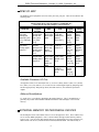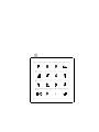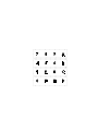
1
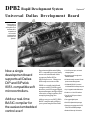
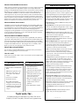
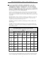
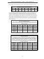
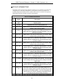
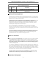
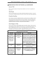
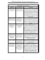
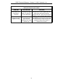
DPB2 Technical Reference
Document Revision 1.3
A Complete
Reference to Using
& Programming the
Universal Dallas
Development
System DPB2
DPB2
LIMITED WARRANTY
The information in this manual is subject to change without notice and does not represent a commitment on the
part of Systronix, Inc. Systronix, Inc. makes no warranty, express or implied, for the use or misuse of its products,
which are provided with the understanding that you, the user, will determine fitness for a particular application.
Systronix assumes no responsibility for any errors which may appear in this manual. No part of this manual may
be reproduced or transmitted in any form or by any means, electronic or mechanical, including photocopying and
recording, for any purpose other than the purchaser's personal use without the written permission of Systronix, Inc.
Systronix reserves the right to revise this documentation and the software and hardware described herein or make
any changes to the specifications of the product described herein at any time without obligation to notify any
person of such revision or change.
TRADEMARKS
Systronix is a registered trademark of Systronix Inc, INTEL and Intel are registered trademarks of Intel
Corporation, Microsoft and MS-DOS are registered trademarks of Microsoft Corporation, OrCAD is a trademark
of OrCAD Systems Corporation.
Systronix®, Inc.
555 South 300 East #21
Salt Lake City, UT 84111
TEL: 801-534-1017
FAX: 801-534-1019
Internet: www.systronix.com
email: [email protected]
Copyright © 1993-1996 by Systronix®, Inc.
All rights reserved.
Revision 1.3 - October 31, 1996
A WORD FROM THE AUTHOR
This manual was created using WordPerfect 7.0. Schematics were created with OrCAD SDT III. Postscript output
was obtained from an Apple LaserWriter IINT. Graphics were created with Generic CADD.
- Bruce Boyes, Systronix, Inc.
DPB2
Technical
Reference
Systronix, Inc.
Complete Solutions for Rapid Development
of Embedded Control Systems
Document Revisions
1.3 Changed programming instructions to recommend not using PR command. Cleaned up some typos
and error in reference to relay outputs. Added references to internet site. Removed A51 assembler
documentation - it is now a separate document.
Table of Contents
DPB2 . . . . . . . . . . . . . . . . . . . . . . . . . . . . . . . . . . . . . . . . . . . . . . . . . . . . . . . . . . . . . . . . . . . . 1
I/O Driver Files . . . . . . . . . . . . . . . . . . . . . . . . . . . . . . . . . . . . . . . . . . . . . . . . . . . . . . . . . . 1
Systronix Web Site & Forum . . . . . . . . . . . . . . . . . . . . . . . . . . . . . . . . . . . . . . . . . . . . . . . 1
Getting Technical Support . . . . . . . . . . . . . . . . . . . . . . . . . . . . . . . . . . . . . . . . . . . . . . . . . . 1
INSTALL BCI51 . . . . . . . . . . . . . . . . . . . . . . . . . . . . . . . . . . . . . . . . . . . . . . . . . . . . . . . . 2
DPB2 Example Program Files . . . . . . . . . . . . . . . . . . . . . . . . . . . . . . . . . . . . . . . . . . . 2
PROCESSOR INSTALLATION . . . . . . . . . . . . . . . . . . . . . . . . . . . . . . . . . . . . . . . . . . . . 2
JP3 2250/2252 Jumper . . . . . . . . . . . . . . . . . . . . . . . . . . . . . . . . . . . . . . . . . . . . . . . . . 2
DALLAS SERIAL LOADERS: IMPORTANT NOTES! . . . . . . . . . . . . . . . . . . . . . . . . . . 3
What are the Dallas Serial Loaders? . . . . . . . . . . . . . . . . . . . . . . . . . . . . . . . . . . . . . . . 3
Loader Script File Tips & Example . . . . . . . . . . . . . . . . . . . . . . . . . . . . . . . . . . . . . . . . 4
KIT5K vs K2 . . . . . . . . . . . . . . . . . . . . . . . . . . . . . . . . . . . . . . . . . . . . . . . . . . . . . . . . 5
Dallas .CFG Files . . . . . . . . . . . . . . . . . . . . . . . . . . . . . . . . . . . . . . . . . . . . . . . . . . . . . 5
PROGRAM vs LOAD . . . . . . . . . . . . . . . . . . . . . . . . . . . . . . . . . . . . . . . . . . . . . . . . . 6
QUICK START . . . . . . . . . . . . . . . . . . . . . . . . . . . . . . . . . . . . . . . . . . . . . . . . . . . . . . . . . 6
File Extensions .SRL and .INC . . . . . . . . . . . . . . . . . . . . . . . . . . . . . . . . . . . . . . . . . . . 6
First Program . . . . . . . . . . . . . . . . . . . . . . . . . . . . . . . . . . . . . . . . . . . . . . . . . . . . . . . . 6
DPB2 I/O MAP . . . . . . . . . . . . . . . . . . . . . . . . . . . . . . . . . . . . . . . . . . . . . . . . . . . . . . . . . 9
Available Processor I/O Pins . . . . . . . . . . . . . . . . . . . . . . . . . . . . . . . . . . . . . . . . . . . . . 9
Address Demultiplexer . . . . . . . . . . . . . . . . . . . . . . . . . . . . . . . . . . . . . . . . . . . . . . . . . 9
EXTERNAL MEMORY OR PERIPHERAL DEVICES . . . . . . . . . . . . . . . . . . . . . . . . . . . 9
Recommended Peripheral Addressing . . . . . . . . . . . . . . . . . . . . . . . . . . . . . . . . . . . . . 10
Protecting Processor Pins from Static or Under-voltage . . . . . . . . . . . . . . . . . . . . . . . 10
POWER SUPPLY . . . . . . . . . . . . . . . . . . . . . . . . . . . . . . . . . . . . . . . . . . . . . . . . . . . . . . . 10
LCD DISPLAYS . . . . . . . . . . . . . . . . . . . . . . . . . . . . . . . . . . . . . . . . . . . . . . . . . . . . . . . 11
LCD Connector Pinout . . . . . . . . . . . . . . . . . . . . . . . . . . . . . . . . . . . . . . . . . . . . . . . . 12
LED Backlights . . . . . . . . . . . . . . . . . . . . . . . . . . . . . . . . . . . . . . . . . . . . . . . . . . . . . 12
20x4 LCD with LED Backlight . . . . . . . . . . . . . . . . . . . . . . . . . . . . . . . . . . . . . . . . . . 13
16x2 LCD with LED Backlight . . . . . . . . . . . . . . . . . . . . . . . . . . . . . . . . . . . . . . . . . . 13
LCD Drivers . . . . . . . . . . . . . . . . . . . . . . . . . . . . . . . . . . . . . . . . . . . . . . . . . . . . . . . . 13
LCD Enclosures . . . . . . . . . . . . . . . . . . . . . . . . . . . . . . . . . . . . . . . . . . . . . . . . . . . . . 13
KEYPAD USE . . . . . . . . . . . . . . . . . . . . . . . . . . . . . . . . . . . . . . . . . . . . . . . . . . . . . . . . . 13
KEYPAD LEGENDS . . . . . . . . . . . . . . . . . . . . . . . . . . . . . . . . . . . . . . . . . . . . . . . . . . . . 16
DIGITAL INPUTS . . . . . . . . . . . . . . . . . . . . . . . . . . . . . . . . . . . . . . . . . . . . . . . . . . . . . . 17
External Input Jumper Blocks JP18 and JP19 . . . . . . . . . . . . . . . . . . . . . . . . . . . . . . . 17
RELAY DRIVER OUTPUTS . . . . . . . . . . . . . . . . . . . . . . . . . . . . . . . . . . . . . . . . . . . . . . 18
BUZZER . . . . . . . . . . . . . . . . . . . . . . . . . . . . . . . . . . . . . . . . . . . . . . . . . . . . . . . . . . . . . 18
ANALOG to DIGITAL CONVERTER . . . . . . . . . . . . . . . . . . . . . . . . . . . . . . . . . . . . . . . 19
ADC Throughput . . . . . . . . . . . . . . . . . . . . . . . . . . . . . . . . . . . . . . . . . . . . . . . . . . . . 19
JP15 I/O CONNECTOR . . . . . . . . . . . . . . . . . . . . . . . . . . . . . . . . . . . . . . . . . . . . . . . . . . 20
APPLICATION EXAMPLES . . . . . . . . . . . . . . . . . . . . . . . . . . . . . . . . . . . . . . . . . . . . . . 21
DPB2 I/O DRIVERS . . . . . . . . . . . . . . . . . . . . . . . . . . . . . . . . . . . . . . . . . . . . . . . . . . . . 21
LOADING PROGRAMS . . . . . . . . . . . . . . . . . . . . . . . . . . . . . . . . . . . . . . . . . . . . . . . . . 21
DEBUGGING DPB2 SOFTWARE and HARDWARE . . . . . . . . . . . . . . . . . . . . . . . . . . . 23
Internet FAQ . . . . . . . . . . . . . . . . . . . . . . . . . . . . . . . . . . . . . . . . . . . . . . . . . . . . . . . . 23
Start Simple . . . . . . . . . . . . . . . . . . . . . . . . . . . . . . . . . . . . . . . . . . . . . . . . . . . . . . . . 23
Exception Handling . . . . . . . . . . . . . . . . . . . . . . . . . . . . . . . . . . . . . . . . . . . . . . . . . . 23
Quick Diagnosis Table . . . . . . . . . . . . . . . . . . . . . . . . . . . . . . . . . . . . . . . . . . . . . . . . 23
SCHEMATICS and MECHANICAL DRAWINGS . . . . . . . . . . . . . . . . . . . . . . . . . . . . . 25
Schematics . . . . . . . . . . . . . . . . . . . . . . . . . . . . . . . . . . . . . . . . . . . . . . . . . . . . . . . . . 27
Enclosure Drawings . . . . . . . . . . . . . . . . . . . . . . . . . . . . . . . . . . . . . . . . . . . . . . . . . . 37
Sample Keypad Legends . . . . . . . . . . . . . . . . . . . . . . . . . . . . . . . . . . . . . . . . . . . . . . . 41
A51 ASSEMBLER . . . . . . . . . . . . . . . . . . . . . . . . . . . . . . . . . . . . . . . . . . . . . . . . . . . . . . . . 43
i
ii
DPB2 Rapid Development System
Systronix®
Universal Dallas Development Board
Rapid application
prototyping and
development for all
the Dallas 8051compatible soft
microcontoller
families with the
new DPB2 from
Systronix.
Now a single
development board
supports all Dallas
DIP and SIPstick
8051-compatible soft
microcontrollers.
Add our real-time
BASIC compiler for
the easiest embedded
control ever!
Experiment with the entire Dallas
8051-compatible processor family
on one convenient board which
accepts any Dallas DIP or
SIPstick processor. Change to a
different processor in seconds.
• 5-13VDC power input, on-board
voltage regulator
DPB2 is a versatile single board
computer with LCD and keypad
interfaces, serial I/O, rugged digital
inputs and outputs, analog to digital
conversion, voltage regulator, and
an ample prototyping area.
• 19.2Kbaud RS232 I/O port and
19.2Kbaud RS232 serial printer port
Add our easy-to-use BCI51PRO
BASIC compiler and you'll have
your system completed in a flash!
• Four rugged digital inputs
• All processor ports brought out to
labelled headers
• 8x2 header easily connects I/O and
power to external equipment
• 4 by 4 keypad encoder/debouncer
• Parallel 4- or 8- bit LCD interface
• Four 350 mA 35V open collector
digital outputs
• 8-bit ADC, adjustable input range
• Generous prototyping area for DIP,
PGA, ZIP and SIMM packages
• Standard 100mm by 160mm size
What are Dallas Soft Microcontrollers?
DPB2 DETAILED DESCRIPTION
Dallas soft microcontrollers are high performance, low power, CMOS systems that
contain the equivalent of a single board computer in one compact SIP or DIP
package. An embedded lithium cell preserves the contents of the on-board code and
data memory (up to 64 Kbytes of each) for 10 years with no external power. A 'T
'suffix (DS2250T, DS5000T, etc) indicates a real time clock and calendar chip
which keeps time for 10 power-off years. Because system code and data memory
is on board, I/O ports need not be used for an address and data bus. Other unique
features include an on-board serial loader, watchdog timer, power-fail interrupt, and
flexible power-up and restart options. Contact Dallas Semiconductor at 972-3714000 or www.dalsemi.com, or follow the links from www.systronix.com.
What is the Dallas Serial Loader?
The Dallas processors have built-in ROM support for serial loading of HEX files.
The Dallas processors’ serial loader is automatically activated by DPB2’s special
reset/load hardware. Using the included software, you can reprogram a Dallas Soft
Microcontroller in seconds over its serial port without changing jumpers or
unplugging and erasing EPROMs. You can encrypt and lock your program or data
to prevent unauthorized tampering - in fact, many bank teller machines are based
on the DS2252 Secure Microcontroller.
What is the BCI51-PRO BASIC Compiler?
...the easiest and quickest way to program an 8051! QuickBASIC users will feel
right at home. BCI51-PRO allows you to program all 8051 and 8052 family parts,
and is the only high level language with specific keyword support for the Dallas
processors. BCI51-PRO includes excellent documentation and support, including a
complete suite of DPB2 I/O drivers. Why struggle with C or assembly? With
BCI51 you can write your application in days instead of weeks.
What if I Want a Custom DPB2?
We can quickly customize DPB2 hardware or firmware to meet your needs and
deliver a working prototype in two to four weeks.
How do I order?
Please refer to our Product Matrix & Price List and Order Form for detailed option
and ordering information.
All systems include:
· DPB2 user manual
· Dallas Soft Microcontroller Data
Book
· DBP2/BCI51 application notes
· Wall cube power supply, 120
VAC input, 6 VDC 300 mA
output
· Systronix A51 assembler
· Serial loader software
· BCI51-PRO and assembly
language source code for reading
the keypad, writing to the LCD,
reading the ADC, reading digital
inputs, and driving the digital
outputs
Stocked Options:
· 4 by 4 splashproof keypad and
cable with connectors
· LCDs: 4 by 20 or 16x2
supertwist with LED backlight
· Rugged, attractive enclosures
with keypad, 20x4 LCD, and a
variety of end panels with
various I/O connections.
· Dallas microcontrollers in 40 DIP
and 40 or 72 SIMM packages
· Compact buzzers and tone
generators
· BCI51-PRO BASIC compiler
Processor sockets 72 SIMM for DS2251, 40 SIMM for
DS2250 and 2252, 40 DIP for DS5000. Crystal, serial and
other I/O ports are common to all processor sockets.
Power Unregulated 6-13 VDC or 5 VDC regulated. 5.5x2.5
mm unregulated input power jack. Regulator input and
ouput are also available at the 8x2 system I/O header. The
regulator is reverse-polarity, short-circuit and overtemperature protected. DPB2 typically consumes 75-100
mA, depending on processor and memory options.
Serial I/O RS232 serial I/O (DB9M) and serial printer
output (5x2 header).
Keypad Encoder A 4x4 keypad encoder interrupts the
processor when debounced keypad data is ready. A patch
area (JP17) is provided to remap keypad row and column
order. Keypad connection is an 8x1 header.
LCD Interface 16x1 header supports intelligent 4- or 8bit parallel-interface LCDs. LED backlight current limiting
resistor and LCD contrast adjustment.
High Current Outputs Four 350 mA, 35 V opencollector relay drivers with snubbing diodes. Connection
via the 8x2 system I/O header.
Buffered Digital Inputs Four rugged inputs withstand
±30 volts and include internal 3 Kohm pulldowns. A
jumper block connects these four inputs to the processor
timer and interrupt pins, or leaves them unconnected.
Connection is via the 8x2 system I/O header.
ADC An 8-bit analog to digital converter with a variable
2.5 to 5.0 reference voltage and an adjustable input
attenuator. At the 5.0 volt reference setting, resolution is
19.6 mV per bit. ADC input connection via 2-pin header
or the 8x2 system I/O header.
Prototype Area 319 plated through holes on .100" centers
in an 11 by 29 grid for any size DIP or PGA, plus two
rows of 29 pads offset by .050" to accommodate ZIP or
SIMM sockets. Heavy power and ground busses on .025"
headers. Every pad is surrounded by ground plane perfect for low-noise analog circuitry.
Expansion An 8x2 system I/O header provides an easy
way to cable digital and analog I/O and power from/to
external equipment. All processor ports and I/O pins are
brought out to labeled .025" square headers on .100"
centers. An HCT573 demultiplexes the address and data
bus for external memory access.
Easy Program Loading Serial program loading can be
initiated by on-card pushbuttons or the RS232 DTR line.
Serial loader software is included. A bicolor LED glows
green when running and red when loading.
Size Standard 100x160 mm single Eurocard size, hundreds
of enclosures available (some stocked by Systronix)
including RF shielded, NEMA rated, etc.
Environmental Commercial temperature range of 0 to 70
deg C.
Support & Warranty Unlimited friendly technical
support. One year warranty against defects.
Systronix Inc.
®
555 South 300 East #21, Salt Lake City, Utah, USA 84111
Tel:(801)-534-1017 Fax:(801)-534-1019 www.systronix.com
rev 1996 Oct 14 bab
DPB2 Technical Reference - October 31, 1996 - Systronix®, Inc.
DPB2
Thank you for purchasing the Universal Dallas Development System DPB2! The current
revision of the DPB2 circuit board is “E”. DPB2 (Dallas Proto Board 2) is the first system
specifically designed to support the entire Dallas Secure Microcontroller family. The unique
arrangement of three sockets enables you to use all three Dallas package types with one
board, and change between them in seconds. DPB2 with BCI51 was voted one of the 100
Hot Products by readers of EDN Magazine. DPB2 is ideal for experimentation and
development as well as incorporation in a finished product.
DPB2 is designed to work with any of the Dallas Soft Microcontrollers. In 1996, Dallas
began referring to these as the Secure Microcontrollers. Systronix has other development
boards designed for the Dallas High Speed Microcontrollers.
DPB2s are in use world-wide in development projects as diverse as DNA replicators, liquid
dispensing systems, vending machines, and electric vehicle motor controllers.
I/O Driver Files
Example programs and I/O "include" files for DPB2 revision E have the letter E in their
name, such as ADC_E.INC. Comments in the file itself also tell you for which version
of hardware the file is intended. Our web site has the latest versions of DPB2 I/O drivers.
Systronix Web Site & Forum
Our web site (www.systronix.com) is the main repository for new DPB2 example code
and I/O drivers. There are links from the web site to an ftp file area. There is also a
forum of Systronix users on the Internet. Our web site has information about joining.
Getting Technical Support
Our technical support is free. We believe good support starts with good written
documentation. If you can’t find the answer in our documentation, then try the FAQ on
the web at www.systronix.com, send e-mail to [email protected], call us at 801534-1017, or Fax us at 801-534-1019. When you contact us, please tell us about any
errors or weaknesses in the documentation so that we can improve it in the next revision.
If you can, please contact us by e-mail first. You can attach a file of source code and
captured output (use MIME encoding if possible) to your message. If you send us an
1
DPB2 Technical Reference - October 31, 1996 - Systronix®, Inc.
example of a problem please make the example as simple as possible, and include any
necessary I/O driver “include” files if you have modified them. We try to answer all email within 24 hours.
Our web site (www.systronix.com) is the main repository for new DPB2 example code
and I/O drivers. There are links from the web site to an ftp file area. There is also a
forum of Systronix users on the Internet - our web site has information about joining.
Please feel free to contact us with any unusual questions about programming DPB2. We
can probably help you approach your needs in the most efficient way. That's why we're
here! Customers consistently give us high marks for courteous, competent technical
support. Tell us how well we're doing for you.
INSTALL BCI51
If you purchased BCI51-PRO, install it now, and while it is self-extracting you can
unpack the DPB2 hardware.
DPB2 Example Program Files
DPB2 example files are in the self-extracting archive DPB2*XMP.EXE where the * will
be used for different versions of DPB2 example code. Some of the DPB2 example files
will overwrite BCI51-Pro files. This is OK.
PROCESSOR INSTALLATION
SIMM parts insert only one way. DO NOT FORCE THEM! SIMM parts have a notch
near pin 1. On DPB2, the SIMM sockets have pins 40 and 72 marked; pin 1 is on the
end of the board closest to the RST/RUN and SLD switches. Insert the SIMM
processors fully into the socket before rotating them into final position and snapping the
metal latches into place. The two plastic posts on the socket should fit easily into the
two drilled holes on the SIMM module.
A 40-pin DIP part has pin 1 located on the notched end of the socket, closest to the
RST/RUN and SLD switches. The DIP40 DS5000 parts have relatively fragile leads so
be careful to line up the part in the socket precisely before pressing it in place. There is
not much clearance between the DIP40 and SIMM40 sockets so be careful when
inserting DIP parts.
This may sound obvious, but - only install one processor at a time!
Some of the signal headers are only applicable to DS2251 or DS2252 or -T (Timekeeper)
components. For example, JP9 is only active with the 2251's special peripheral bus.
Refer to the DPB2 schematics and the Dallas data sheets for processor pinout details.
JP3 2250/2252 Jumper
If you are installing a SIMM40 processor, place JP3 in the proper position. This jumper
affects ONLY the SIMM40 socket and has no effect on DIP40 or SIMM72 parts.
2
DPB2 Technical Reference - October 31, 1996 - Systronix®, Inc.
Pin 20 of the DS2252 is the self-destruct input, active high. (No, the processor won’t
explode if this pin is high.) If JP3 is in the 2250 position and you install a DS2252
processor, your 2252's program will be erased.
On the DS2250 pin 20 is the EA (external access) pin. With a DS2250 processor, pin 20
should be pulled high (JP3 in the 2250 position) to enable the DS2250's on-board
memory and embedded clock. If left to float, it will be pulled low with its internal pulldown, disabling the on-board memory and clock and causing the DS2250 to act like a
plain 8031 with no on-board memory.
DALLAS SERIAL LOADERS: IMPORTANT NOTES!
You are, of course, eager to use your new DPB2 system, but please take the time to
read the following quick start and loader tool information. It will only take a few
minutes and could save you needless frustration. The loading process is simple, but it
must be followed exactly, and you must give the loader the proper memory map
parameters. These tips will help you get up and running quickly and easily.
It's tempting to jump into a complex application right off the bat, but please run one of
the supplied sample programs first. This will verify that your PC, cable, hardware and
installed software are all working together, and that you understand the complete
compile-and-download process.
What are the Dallas Serial Loaders?
The Dallas serial loaders are PC-DOS programs which use your PC’s RS-232 serial port
to communicate with a Dallas Secure Microcontroller. The loaders provide Intel HEX
file transfer. They also provide Secure Microcontroller configuration such as memory
mapping, locking, etc. Finally, the loaders include a terminal emulator which you can
use to communicate with your application via serial I/O.
The Dallas Secure Microcontrollers have a “hidden” internal ROM which gives them
their built-in ability to be reloaded in-circuit, via their serial port. This hidden ROM is
accessed by resetting the part in a special way to invoke the serial load mode. Details on
invoking serial load mode are in the Dallas data book. You can easily add this ability to
your own custom hardware.
DPB2 has this serial load mode ability built in. When in serial load mode, your
application is mapped out, and the hidden internal ROM is mapped into, the controller’s
memory. When the controller is reset, the hidden ROM is disabled completely, and your
program and data space is mapped back into the controller’s memory. It’s a very clever
system. The loader ROM and your application can never interfere with each other. This
is why your application program running on the Secure Microcontroller cannot call or
otherwise execute the serial loader. Your application and the serial loader are mutually
exclusive.
DPB2 and the Dallas PC software use DTR coming from your PC to trigger the serial
load mode. When DTR is asserted, DPB2's status LED glows red. When in normal
reset/run mode, the LED is green.
3
DPB2 Technical Reference - October 31, 1996 - Systronix®, Inc.
The Dallas loaders have on-line help at both the KIT prompt and the TE level. At the kit
prompt, just type “help” for a list of commands, or “help {command}” to get detailed
help on a specific command, for example “help load” for detail on LOAD. At the TE
prompt, press the ESC key first to enter TE command mode, then type help.
You MUST use the correct Dallas loader - KIT5K for DS5000 and DS2250, K2 for
DS5001, DS5002, DS2251 and DS2252. Using the wrong loader will give unpredictable
results such as inability to access any BASIC variables in data memory.
If you are using the DS5000 or DS2250 family with the KIT5K loader, do NOT use the
PROGRAM command. There is a bug in the KIT5K loader. The bug sometimes (but
not always) fails to properly set the RANGE and PARTITION of DS5000 or DS2250
parts. However, this is not really a problem since the PR (PROGRAM) command is not
the best way to load programs anyway. It is quicker and requires far less repetitive typing
if you use loader script files which contain the LOAD and (optional) VERIFY
commands. Loader script files work in a manner similar to DOS BATCH files.
Loader Script File Tips & Example
The Dallas loaders - both KIT5K and K2 - can be invoked with a script file as a
command line parameter, for example, at the DOS command line, type “KIT5K mycode”
(don’t type the quotes) to invoke KIT5K with the script file MYCODE. (Command lines
and script files are not case sensitive.) This starts the loader KIT5K and instructs it to
open the DOS file mycode. All loader commands in the file will be executed exactly as if
you had typed them by hand.
Loader script files are very similar to DOS BATCH files. They are simply ASCII text
files with one command on each line of the file.
Script files are a great timesaving convenience for several reasons. First, the PR
(PROGRAM) command is buggy. DO NOT USE the PR command. It often does not set
the range and partition correctly. It may work fine 500 times and then fail a dozen times
in a row, as strange as that seems. (Don’t ask us why - we didn’t write it.) Second, a
script file is faster than manually typing the commands. Third, you can set the baud rate
as high as possible so loading is faster. If your application uses a lower baud rate for
serial communication, the script file can set it back after downloading your program and
before starting the loader’s Terminal Emulator program. Fourth, since the script file can
contain explicit configuration information, you don’t have to fuss with the “.CFG”
config files (discussed below).
There are several script file examples on your disk. They typically have the same file
name as .BAS and .HEX program files, but with no file extension. Here is one example
of such a script file. This script file sets COM1, forces serial load mode. It sets the
download speed to 19200 baud. Then it sets RAnge and PArtition. Then it LOADs the
file ecc4.hex. Then it sets the speed of the COM port back to 9600 (since that's what the
program ECC4 uses). Then it turns off DTR (we know it was on because of the prior
PGMODE). Then it starts Terminal Emulator mode. That's it!. Notice that the example
doesn't use VERIFY. I've never had a verify fail in over 5 years, and not using it cuts the
programming time in half.
Note that the PGMODE command is NOT the same as PR command. PGMODE forces
DTR on regardless of its current state. The DTR command toggles DTR, so it is only
useful if you are certain of it’s current state. The loader assumes all RANGE and
4
DPB2 Technical Reference - October 31, 1996 - Systronix®, Inc.
PARTITION values entered are in hexadecimal format. Don’t enter decimal numbers or
the loader will use incorrect locations.
Suppose this file name is ECC4 (with no extension to keep it short). Invoke it from the
DOS command line:
kit5k ecc4
Here's the contents of script file ecc4:
com 1
pgmode
speed 19200
ra 8000
pa 6000
load ecc4.hex
speed 9600
dtr
te
You can make a script file for every program you will be loading frequently, and give it
the same name as the program without an extension.
And here's a final tip: rename KIT5K.EXE to K1.EXE, then your loaders are K1 for the
DS5000 family and K2 for the DS5001/2. It saves some typing and makes the names
consistent.
KIT5K vs K2
The K2 loader sets additional memory partition control bits of the DS5001/2 family.
The KIT5K loader does not understand the newer Dallas parts. Using the KIT5K loader
with DS2251 or DS2252 parts will not properly set the memory map. Your program
MUST have a properly configured memory map in order to run correctly.
Dallas .CFG Files
When you use the Program command without a script file (remember to only use PR
with the K2 loader, never with KIT5K), the Dallas loaders set the memory map, lock bit,
etc. according to an existing .CFG file, if any. If a .CFG file does not exist, the loader
prompts you for input. For example, if you are loading program ECC4.HEX, the loaders
will search for ECC4.CFG and use it, even if its settings are completely wrong for your
program. This is because the BCI51 directives such as #TARGET, #DATA START,
and #CODE START do not automatically update the .CFG file, nor do they set the
memory map and other target options (yes, we plan to change this in a future release of
BCI51). These options must be set by the loader and you must tell the loader what these
values are. Therefore, if you change your program's configuration, you should either
delete the .CFG file or edit it to bring it into conformance with your new .HEX file.
You can edit the .CFG file with a text editor or by using the /edit switch with the
PROGRAM command:
pr ecc4.hex /edit
for example. This will prompt you line by line to change the .CFG information.
5
DPB2 Technical Reference - October 31, 1996 - Systronix®, Inc.
If you use a script file, then the limits of a .CFG file do not apply, since the script file
can contain explicit range and partition information. This is another reason to use script
files.
PROGRAM vs LOAD
The Dallas loader LOAD command differs significantly from the PROGRAM command.
The PROGRAM command sets the memory partition, lock bit, etc, and verifies the
.HEX file you program. The PROGRAM command uses the values in the .CFG file, or
prompts you for values if no .CFG exists.
The LOAD command does not use the .CFG file, nor does it set the memory partition.
In other words, if you LOAD a HEX file, it will be stored with the same configuration
values as existed previously in the target. LOAD is significantly faster than
PROGRAM. If you are repeatedly editing, compiling and downloading an application,
LOAD can save you a lot of time. But if your previous program had a different memory
partition, LOADing a new HEX file will preserve the old settings which are incorrect for
the new HEX file, and your new program will not execute properly. The solution is
simple - load the new program with the PROGRAM {hexfilename} /EDIT command,
after which you can subsequently load compatible versions with the LOAD command.
Better yet, use a script file.
QUICK START
If your DPB2 is assembled and has the processor installed, we have tested and initialized
it with a sample program. In this case, simply connect any accessories such as your LCD
and keypad, connect the wall cube power supply, and DPB2 should immediately boot up,
the LED should be green, and the application should begin running.
If the LED is red, your PC is asserting the DTR line. Unplug the serial cable from DPB2
and press the reset switch S1. The LED should change to green and DPB2 should begin
running.
Some PC software asserts DTR upon exit, so you may need to disconnect DPB2 from
your PC when you are not running the Dallas serial loader software.
File Extensions .SRL and .INC
The file extension .SRL stands for “SouRce Library”. SRL files contain serial I/O
drivers, math operations, and other library support code to implement the BASIClanguage syntax in BCI51 programs. Include files with an extension “.INC” are used to
implement functions which are not part of BCI51 BASIC such as LCD access, analog-todigital conversion, keypad input, and so forth.
First Program
Try the following example programs as your first use of DPB2 and BCI51. Please jump
ahead to the section DPB2 I/O DRIVERS on page 21 and read it, then return here.
6
DPB2 Technical Reference - October 31, 1996 - Systronix®, Inc.
Copy the original BCI51 file USER.SRL to USERORIG.SRL or some other
convenient name so that you have an unmodified spare copy, then copy the file
USERDPB2.SRL to USER.SRL. USERDPB2.SRL is a version of the USER.SRL
library which has been modified to support DPB2 I/O such as the LCD. You MUST use
the drivers in USERDPB2.SRL in order for the sample programs to properly access
the LCD, keypad, ADC, and other DPB2 peripherals.
Open the recommended program with an editor and make sure your target and memory
map are correct, as recommended in the Quick Start Configuration table. Leave baud
rate unchanged, since it should be correct for the Dallas loader software script files which
we provided.
20x4 LCD: DPB2E_X.BAS, for DS2250 or DS5000 targets, DPB2E_X1 for 2251 and
2252 targets. The “X” is the current revision of the program, “E” at the time of this
writing but may be different on the disk you receive.
16x2 LCD: LCD162.BAS, for DS2250 or DS5000 targets, LCD162_1.BAS for 2251
and 2252 targets.
No LCD: ECC4.BAS for DS5000 and 2250 targets, ECC4_51.BAS for DS2251 and
DS2252 targets. This program is good for initializing the embedded clock and calendar
of new Dallas processors.
RECOMMENDED QUICK START CONFIGURATION
All numerical values are hexadecimal, except RANGE values of 64 and 128 which are
KBytes
BCI51 Compiler Configuration
Dallas Loader Configuration
Processor
#Target
#Code
Start
#Data
Start
Loader
RANGE
PArtiti
on
DS5000T32
DS5000
T
0
6000
KIT5K
8000
6000
DS2250T32
DS2250T64
DS2250
T
0
6000
8000
KIT5K
8000
6000
DS2251T64
DS2251
T
0
8000
K2
64
8000
DS2251T128
DS2251
T
0
0
K2
128
0
DS2252T64
DS2252
T
0
8000
K2
64
8000
DS2252T128
DS2252
T
0
0
K2
128
0
First, be sure that your sample program has the correct #TARGET and #DATA START
values. (For Dallas targets, #CODE START should always be 0H). Refer to the table
7
DPB2 Technical Reference - October 31, 1996 - Systronix®, Inc.
above for some guidelines.
Compile your program by invoking BCI51 on it. For example, if you are using a
DS2250T target and a 20x4 LCD, at the DOS command line type
BCI51 DPB2E_E -o
The switch “-o” (the letter o, not the numeral 0) invokes the BCI51 optimization option.
After the compilation is complete, this will create a file DPB2E_E.HEX. Connect a
standard (all pins wired straight through) serial cable from your PC to DPB2. Do not
use a null modem cable (pin 2-TXD and pin3-RXD swapped).
Before you use a script file, try it one time manually, so that you understand what the
script file does. Start the Dallas loader - in the DS2250T case,
KIT5K
Type the PC's COM port you are using such as
COM 1
The LED on DPB2 should switch from green to red to indicate loading. If the LED
remains green, type PGMODE to force DPB2 into load mode. Now type
ST
for status. You should see a couple of lines of configuration information. If the range and
partition are not correct for your program (refer to the table above), change them with the
RANGE and PARTITION commands. You can save some typing by using their short
forms RA and PA. For example, for a DS2250T-32 processor with the program
DPB2E_E, type
RA 8000
PA 6000
You can use the ST command again to verify that the values are correct. If they are, type
LOAD DPB2E_E.HEX
The program will load. If you wish you can type
VERIFY DPB2E_E.HEX
to verify that the program in the controller is the same as the HEX file on your PC. Now
start the Terminal Emulator so that you can see output from DPB2:
TE
starts the Dallas terminal emulator. In the terminal emulator, press and release the ESC
key to enter command mode, and then type
DTR
to turn off the DTR line. When you press ENTER to complete the DTR command, TE
changes back to communication mode rather than command mode. The DPB2 LED
should change from red to green. You should see a message on the status line at the
bottom of your PC's screen and the sample program should be off and running, with
output something like this:
> LCD init
DPB2E DS5000/DS2250 family serial output test:
ABCDEFGHIJKLMNOPQRSTUVWXYZabcdefghijklmnopqrstuvwxyz0123456789!@#$%^&*()_+
Example Program DPB2E_E
8
DPB2 Technical Reference - October 31, 1996 - Systronix®, Inc.
DPB2 I/O MAP
The DPB2 on-board peripherals use some of the processor port pins. These are described in the
following table.
PROCESSOR PINS USED BY DPB2 I/O PERIPHERALS
Note: this I/O map may change in future revisions
Serial I/O
Keypad
Encoder
ADC
LCD
Digital
Inputs
Relay
Drivers
The main
RS232 port
uses P3.0 and
P3.1, RXD and
TXD.
Keypad data
D0..D3 use
Port 0, bits
0..3 (P0.0P0.3)
P0.4 is the
ADC serial
data
LCD data
uses Port 0
bits 0-7
(P0.0-P0.7).
Digital
input 0
can use
P3.2
(INT0)
Relay
data is
P0.0P0.3
The serial
printer output
uses P1.7
Keypad
interrupt uses
the processor
INT1 input,
P3.3
P1.0 is the
ADC chip
select,
active low
LCD RS
uses P1.4
Digital
input 1
can use
P3.3
(INT1)
Relay
register
strobe is
P1.1
Keypad read
enable strobe
uses P1.3
P0.5 is the
ADC clock
which
shifts out
data
LCD Read
strobe uses
P1.5
Digital
input 2
can use
P3.4 (T0)
Relay
output
enable is
P1.2
LCD EN
strobe uses
P1.6
Digital
input 3
can use
P3.5 (T1)
Available Processor I/O Pins
All eight bits of Port 2 are unused (P2.0-P2.7), as are P3.6 (WR), and P3.7 (RD). P3.2 (INT0),
P3.3 (INT1), P3.4 (T0), and P3.5 (T1) can be used as external digital inputs by jumpering JP18
and JP19 appropriately. RP1 pulls up Port0, the AD0-AD7 bus, since Port0 has open drain
outputs.
Address Demultiplexer
U7, an HCT573, is provided to demultiplex the address/data bus. The U7 demultiplexer is
generally only useful on the DS5000 and DS2250 families with 64 KBytes or less of total
memory.
EXTERNAL MEMORY OR PERIPHERAL DEVICES
The demultiplexed low-order address lines A0-A7 are brought out to JP13. These address lines
are not used by DPB2 peripherals. Port 2 is unused and is the high external memory address
byte A8-A15. You can easily add external memory or peripheral devices to the prototype area,
address them with A0-A15, and strobe them with WR, RD and PSEN. External memory or
9
DPB2 Technical Reference - October 31, 1996 - Systronix®, Inc.
peripheral devices will need to share the data bus Port 0, D0-D7. If you wish you could add a
buffer such as an HCT245 between Port0 and other data devices.
Please note that Dallas devices access off-chip data or code memory in special ways compared
to generic 8051 processors. Please refer to the Dallas Soft Microcontroller Data Book (1993), or
the new Secure Microcontroller and BCI51 compiler documentation for the Dallas processors.
Recommended Peripheral Addressing
If you wish to add more peripherals to DPB2, we recommend that you use the approach we have
taken with the existing DPB2 peripherals. We use PORT0 as the bidirectional data bus and
other pins from PORT1 and PORT3 as chip enables and strobes. You can use the WR and RD
pins (P3.6 and P3.7) as external read and write strobes and drive them explicitly with firmware.
Generic 8051 processors do not have "external data memory" on board. Dallas processors do.
This makes traditional 8051 memory-mapped I/O less attractive for Dallas processors, especially
those with 128 KBytes of memory.
On Dallas targets with a full 64 KBytes of data memory, and some with 32 KBytes of data
memory, you can't memory map I/O without losing access to a block of your on-board data
memory. A notable exception is the DS2251 which has a separate byte-wide peripheral data bus
with 15 address lines and two chip selects. This peripheral bus is completely independent from
the processor ports PORT0, PORT1, PORT2, and PORT3.
Dallas processors have a wide variety of memory map options which are too detailed to repeat
here. Please refer to the Dallas Soft Microcontroller Data Book, 1993 or later, for all the details.
Protecting Processor Pins from Static or Under-voltage
If you will be accessing machinery or equipment attached by cables to the address and data
busses of DPB2, you will need to buffer them or at least protect them against static or under
voltage conditions before they leave DPB2. Do not wire controller pins directly to a cable
which drives a printer or other device. Page 60 of the 1993 Dallas Soft Microcontroller Data
Book shows a combination of schottky diodes and 1K ohm resistors to protect processor port
pins from negative voltages.
Keep LCD cables less than 12 inches long since these are directly driven by Port 0. It is possible
to drive cables as long as 15 feet (we've done this just to prove a point) but bus settling time and
ringing become significant. Long cables add capacitance which increases settling time on Port 0.
Static discharge is also a concern since the static could directly contact the processor device
pins.
Mount the LCD in an enclosure or panel which will withstand or redirect a static discharge. The
keypad is isolated from the processor by the 74C922, so you do not need to worry about keypad
cable length of a few feet.
Relay driver cables can safely be several feet in length, since the relay drivers are designed to
drive high capacitance loads. The DPB2 buffered digital inputs have a 1489 type buffer, the
same as used on commercial RS-232 ports. It is quite robust and can withstand a DC level of up
to ± 30 volts, as well as 500 volts or more of static discharge.
POWER SUPPLY
The power input jack is 5.5 x 2.5 mm, with center terminal positive and the sleeve negative.
10
DPB2 Technical Reference - October 31, 1996 - Systronix®, Inc.
The DPB2 voltage regulator will run cool if your supply is in the 6 to 7 volt RAnge. If you are
using a lot of high-current devices in the prototype area, you may need a larger supply. The
DPB2 card draws less than 100 mA without an LED-backlight LCD. An LED backlit LCD can
add an additional 200 mA, depending on the value of backlight current limiting resistor R6.
If you provide your own power supply be sure it is a DC voltage of 6 to 13 volts. Some wall
cube power supplies are actually AC transformers and may damage DPB2. A 6V 800 mA
supply is included with your assembled DPB2 order. If you provide your own supply, allow 100
mA for DPB2 plus an additional 100 to 200 mA if you will be using an LCD with LED
backlighting. LED backlights vary greatly - we have seen some as high as 400 mA on a 20x4
LCD. The 20x4 LCD provided by Systronix typically draws 100 to 120 mA.
Higher power supply input voltages will work, but will cause the regulator to dissipate any
wasted power. For example, if the DC input is 12 volts and you are using an LED backlight at
200 mA and the DPB2 with prototype area circuits draws 100 mA, then the regulator will
dissipate (12-5) x 300 mA = 2100 mW or 2.1 watts. This will feel quite warm to the touch.
With a 6V supply such as we sell, the regulator only dissipates (6-5) x 300 mA = 300 mW. The
regulator will simply shut down if it overheats and will turn on again when it cools off.
If you will be driving DPB2 from a 12 VDC vehicle electrical system, the input voltage will
typically be 13.8 VDC. You may wish to add series diodes or a dropping resistor to avoid
overheating the DPB2 regulator U12.
LCD DISPLAYS
DPB2 has a 16x1 0.100-inch pitch connector for an intelligent parallel-interface LCD.
Potentiometer VR1 provides LCD contrast adjustment. When you first plug in an LCD cable,
don't panic if your display is blank - it may simply be that the LCD contrast needs to be
increased. If the display is black, contrast is too high. To the left of the display connectors,
pads are provided for an LED backlight current limiting resistor R6, nominally 10 ohms. Pins
15 & 16 of the LCD connectors are the + and - of the LED backlight. Pin 15 is tied to 5 VDC
through the current limiting resistor R6, typically 10 ohms. Pin 16 is ground.
Please note that we are phasing out our 24x2 LCD. It is replaced by a 16x2 LCD available with
an LED backlight. The 16x2 is more typically mounted in the front panel of a machine or
custom enclosure, rather than our handheld enclosure.
11
DPB2 Technical Reference - October 31, 1996 - Systronix®, Inc.
LCD Connector Pinout
LCD connector U8 pinout is described in the following table.
U8 LCD CONNECTOR PINOUT
Pin
#
Signal
Input/Output
Description
1
VSS/GND
Power
System ground.
2
VCC/+5
VDC
Power
Powers LCD logic and controller (not the
backlight).
3
VEE
Input
LCD contrast adjustment, driven by the
VR1 wiper.
4
RS
Input
Register select. Low selects instruction
register for write, busy flag for read. High
selects data register for read or write.
5
R/W
Input
Read/write strobe. Low to write to the
LCD, high to read from the LCD.
6
E
Input
Enable strobe. Initiates all LCD access
cycles.
7
DB0
Input/Output
LCD data bit 0. All DB lines float high
impedance when the enable strobe is low.
8
DB1
Input/Output
LCD data bit 1
9
DB2
Input/Output
LCD data bit 2
10
DB3
Input/Output
LCD data bit 3
11
DB4
Input/Output
LCD data bit 4
12
DB5
Input/Output
LCD data bit 5
13
DB6
Input/Output
LCD data bit 6
14
DB7
Input/Output
LCD data bit 7
15
LEDA
LED Power
LED backlight anode, needs a current
limiting resistor in most cases. Some
LCDs have a built in limiting resistor,
including those currently supplied by
Systronix (this is subject to change).
16
LEDK
LED Power
LED cathode, generally grounded. Or
drive this with an open collector relay
output to turn the backlight on and off
under firmware control.
LED Backlights
If you are using an LED with no backlight, it may be easier to connect a ribbon-cable to the
JP14 or U8 headers if you snip off the unused backlight pins 15 and 16.
12
DPB2 Technical Reference - October 31, 1996 - Systronix®, Inc.
Densitron LCDs do not use pin 16 of the LCD connector, since they share a common ground
(pin 1) between the LCD logic and the LED backlight. DPB2-E is designed so that both the
Densitron and 2-conductor LED backlights are correctly powered.
Resistor R6 provides backlight current limiting. Forward voltages of LED backlights are
typically in the range of 4.0 volts. A 10 ohm R6 thus provides 100 mA of backlight drive
current.
20x4 LCD with LED Backlight
The Systronix 20x4 LCD with LED backlight currently has a built-in current limiting resistor.
Earlier Systronix LCDs did not. We will ship the proper LCD/DPB2/R6 combination. Call us or
check the Internet for current version details. This LED backlight uses both pin 15 and pin 16 of
the DPB2 LCD connector. You can add a resistor to R6 to reduce the power consumption of the
LCD backlight. The LCDs Systronix provides are chosen for high contrast, wide viewing angle,
and even, efficient LED backlight. Our LED backlights use less than half the current of some
name-brand LCDs.
16x2 LCD with LED Backlight
The Systronix 16x2 LCD with LED backlight has its own built in (typically 27 ohm) current
limiting resistor, so it does not require current limiting resistor R6. This LED backlight does not
use pin 15 and pin 16 of the DPB2 LCD connector. It derives the LCD LED backlight power
from pins 1 and 2 of the LCD connector.
LCD Drivers
Files LCD*.INC include a library of routines, mainly for a 20x4 LCD. File HELLO242.BAS
includes sample code for a 24x2 LCD. LCD162.XXX are sample programs for a 16x2 LCD.
Other drivers may be on your disk. Current drivers are available from our Internet site.
LCD Enclosures
Currently our enclosures are available for both 20x4 and 16x2 LCDs. The 20x4 LCD is more
popular, since it fills the enclosure width better and is more aesthetically pleasing. The 20x4
LCD is more practical for creating multi-level menus and detailed data displays than the 16x2.
The 16x2 is smaller and less expensive.
KEYPAD USE
Connect a "matrix-pinout" keypad with up to 4 rows and 4 columns to the 1x8 header U10.
Keypads are available from Systronix and many electronic supply distributors. Membrane
keypads with a flex cable tail usually have a color dot or arrow on pin 1 of their 1x8 receptacle.
JP17 is provided to map your keypad's row and column order to the U9 keypad encoder's input
pins. JP17 has rows 1-4 labeled as X1-X4, and columns 1-4 are Y1-Y4. JP17 has straightthrough connections on the back side of the PC board connecting its even pins (which come
from the keypad header U10) to its odd pins (which are connected to the 74C922 keypad
encoder).
Our enclosure 100205-100 has a recess milled to accept our 4x4 keypad 100222-100.
If your keypad requires significantly different row and column wiring, you can cut the traces on
13
DPB2 Technical Reference - October 31, 1996 - Systronix®, Inc.
the back of the PC board and wire-wrap, solder, or jumper whatever connections you need.
EXAMPLE KEYPAD CONNECTOR PINOUT
8
7
6
5
4
3
2
1
ROW4
ROW3
ROW2
ROW1
COL4
COL3
COL2
COL1
If your keypad does not have the above pinout, don't panic! As long as your keypad rows and
columns are connected to any rows and columns of the 74C922, you can correct other wiring
easily in a keypad lookup table. Examples are included in your DPB2 firmware disk. For
example, you can fix a swap between row 1 and row 4 in a lookup table. The file LCD222.INC
(in the example file DPB2DXMP) in fact does this to correct a row swap of rows 1 and 2 in our
keypad 100222-100 on the older DPB2 rev D. But if a keypad row is swapped with a keypad
column it may not be possible to sort this out in a lookup table. Files KEY*.INC include other
sample keypad code.
KEYPAD ENCODER MAPPING
This is what the output of the 74C922 would be for an ideal keypad wired
straight to the 922 with all keypad rows and columns matching the 922's row
and column inputs.
ROW/COL
Col Y1
Col Y2
Col Y3
Col Y4
Row X1
0
4
8
12
Row X2
1
5
9
13
Row X3
2
6
10
14
Row X3
3
7
11
15
KEYPAD 100222-100
This map shows the value of each key as if it were written on the keypad. As
you press keys on the keypad and read their hexadecimal value from the
74C922, this is what you would obtain. Note that rows 1 and 2 are swapped in
the keypad. Note that this mapping assumes pin 1 of the keypad connector to
be the rightmost pin as you face the keypad with the connector tail emerging
from the top of the pad.
ROW/COL
Col 4
Col 3
Col 2
Col 1
Row 1
D
9
5
1
Row 2
C
8
4
0
Row 3
E
A
6
2
Row 4
F
B
7
3
14
DPB2 Technical Reference - October 31, 1996 - Systronix®, Inc.
DESIRED KEYPAD LAYOUT
This possible keypad layout is similar to the numerical keypad on your PC. The
left arrow is the backspace/rubout key. This is the standard keypad legend
layout we provide with our 4x4 keypad 100222.
7
8
9
4
5
6
1
2
3
ESC
0
.
ENTR
The easiest way to remap keys is in a lookup table. The file KEY_E.INC illustrates this. The
lookup table also appears here:
key_get_val:
gosub key_get_data
#ASM
mov
DPTR,#__KEY_DAT
; addr in DPTR
movx A,@DPTR
; put value into acc
add
A,#02H
; adjust for jump
movc A,@A+PC
; get lookup value into acc
sjmp OVER_KEY_TABLE
; jump over data
;
; lookup data entries
; this translates Systronix keypad 100222 into the keys used
; in our HPC1 system. Note that pin 1 of the keypad connector is
; the rightmost pin as you face the keypad with the flex cable
; extending away from you, out of the top of the keypad.
;
; 1xH are the non-numeric keys
DB
14H
; 0 - del/backspace;
DB
15H
; 1 - up arrow
DB
13H
; 2 - down arrow
DB
12H
; 3 - enter
DB
06H
; 4 DB
09H
; 5 DB
03H
; 6 DB
11H
; 7 - dec point
DB
05H
; 8 DB
08H
; 9 DB
02H
; A DB
00H
; B DB
04H
; C DB
07H
; D DB
01H
; E DB
10H
; F - escape
OVER_KEY_TABLE:
movx
@DPTR,A
; store value in KEY_DAT
#ASM_END
return
If you have a 20x4 LCD, program DPB2E_B.BAS includes a routine which displays the original
and remapped key values on the LCD.
15
DPB2 Technical Reference - October 31, 1996 - Systronix®, Inc.
KEYPAD LEGENDS
If your ordered a keypad and enclosure from us, they will probably be delivered assembled and
tested, with the keypad legends shown on the attached mechanical drawing.
16
DPB2 Technical Reference - October 31, 1996 - Systronix®, Inc.
The keypad 100222-100 is also available with no imprinted legends. In this case, it comes in
two pieces: the actual membrane keypad and a protective overlay with a clear area for each key.
You can easily create your own legends on a word processor or drawing program. Copy them
onto 20 lb bond paper on a laser printer (heavier paper reduces tactile feedback). Or you can use
a color photocopy of a color inkjet print for a more elaborate custom appearance. You can
easily and quickly make low-volume custom keypads which look like they are an expensive fullcustom design.
The keypad and its protective overlay are intended to be held together by the adhesive strips on
the keypad. Position your legends (either in strips or a whole sheet) over the keypad. Peel off
the adhesive release liner and position your legends. Be sure your legends are small enough to
leave a border of adhesive around them to hold the overlay. Press the overlay carefully in place.
This adhesive is very tenacious, so you only get one attempt at this!
If you leave one edge of the release liner in place you can create a "pocket" between the keypad
and overlay to let you insert different key legends at any time.
Finally, the keypad back also has laminated adhesive for permanent mounting to an enclosure or
panel. Be sure the mounting surface is clean - some isopropyl alcohol will remove any grease or
oil from plastic and metal surfaces. Line up the keypad carefully since the adhesive is very
permanent and cannot be easily repositioned.
DIGITAL INPUTS
The external digital inputs of DPB2 have a robust buffer which will withstand ±30 volts without
damage. It has internal pull-down of approximately 3K ohms. This 14C89A buffer inverts the
input, therefore a floating external input is pulled low at the buffer input and when inverted,
generates a TTL high at the processor pins. This is convenient, since the external inputs INT0,
INT1, T0 and T1 are active low. An external switch, then, should be wired to drive the external
inputs high for an active state. This will produce a low at the processor pins.
If you want active low external inputs, you can install a 1K ohm pull-up resistor pack in RP3 and
a link in JP20 to pull-up the external inputs.
External Input Jumper Blocks JP18 and JP19
The jumper blocks JP18 and JP19 provide for mapping the external inputs and keypad interrupt
to the processor INT0, INT1, T0 and T1 inputs.
17
DPB2 Technical Reference - October 31, 1996 - Systronix®, Inc.
JP18 & JP19 OPTIONS
* means has no effect
JP18
JP19
Description
T1 installed
KPD
position
Keypad interrupt to processor INT1 (P3.3), external
interrupt 1
EXT
position
External input 1 to processor INT1 (P3.3), external
interrupt 1
*
removed
Processor INT1 not connected to keypad or external input
1
T1 removed
*
Processor INT1 not connected to keypad or external input
1
T0 installed
*
External input 0 to processor INT0 (P3.2), external
interrupt 0
I0 installed
*
External input 2 to processor T0 (P3.4), Timer 0
I1 installed
*
External input 3 to processor T1 (P3.5), Timer 1
removed
*
Processor INT0, INT1, T0 and T1 not connected to any
external inputs
RELAY DRIVER OUTPUTS
Relay driver pins are available on the JP15 8x2 I/O connector. A table of pin designations is on
page 20. You should tie Vk to the supply voltage which powers your relay outputs. For example
if you are driving relays from a +12V supply, tie Vk to the source of the 12V supply. This will
tie the snubber diodes in the relay drivers to the +12V rail. The outputs can sink a maximum of
500 mA and hold off 50 Volts. Nominal ratings are 350 mA at 12-20 volts. If you will be
driving all outputs simultaneously, limit each output to 250 mA. If you wish, outputs can be
wired in parallel for greater sink current capability.
Since these are open collector outputs you may need to provide your own pull-up resistor,
depending on what you're driving. These outputs cannot source current, they can only sink it.
The relay outputs invert, so writing a "1" to a relay bit drives that output low and causes it to
sink current. Writing a "0" to a bit causes it to be released to float high, assuming you have an
external pull-up resistor. With no external pull-up, an output will float around 1 volt.
Files RELAY*.INC include code for clearing and accessing the relay drivers.
BUZZER
You can easily drive our buzzer part number 100201 directly from the relay driver. This buzzer
includes a built in oscillator - all you need to do is supply power and it will buzz. Just tie the
positive (longest) lead of the buzzer to 5 volts, and the negative lead of the buzzer (shortest lead)
to the relay driver output. Some of the DPB2 sample programs already assume a buzzer is
attached to the least significant bit of the relay driver.
18
DPB2 Technical Reference - October 31, 1996 - Systronix®, Inc.
Asserting the relay output causes the buzzer to emit a tone. The sample programs
(DPB2E_X.BAS where X is the current revision) include a routine which creates a brief audible
click when a keypad key is pressed, as well as a longer beep when other keys are pressed.
ANALOG to DIGITAL CONVERTER
An 8-bit ADC is provided on DPB2, with a reference adjustment VR2, and input labeled at JP16.
You can adjust the reference continuously between 2.5 and 5.0 volts. This gives your
conversions a resolution of 9.8 mV to 19.6 mV per bit. Resistors R10 and R9 are an input
attenuation network. If you increase R10 you can increase the input range of the ADC.
VADC = VINPUT * R9/(R10 + R9)
For example, if R10 is 10 Kohms, the input range of the ADC will be 0-10 volts. DPB2 ships
with R10 of 10 ohms, in which case the input range is 0-5 volts.
FILE ADC*.INC includes code to read the ADC. Program DPB2E_B.BAS demonstrates this
also.
ADC Throughput
The TLC549 ADC conversion time is typically 17 usec. Total access and conversion time is 25
usec. This allows up to 40,000 conversion and access cycles per second. As a practical matter,
this is limited by the speed of the 8051 at 12 or 16 MHZ and the rate at which your application
can process the ADC data.
The driver in ADC_E.INC takes about 50 usec (at 12 MHZ) to read the ADC value. If you store
the value in memory and/or manipulate it with BASIC instructions this will add more time. A
reasonable throughput estimate at 12 MHZ might be anywhere from hundreds to a few thousand
samples per second, depending on your application.
19
DPB2 Technical Reference - October 31, 1996 - Systronix®, Inc.
JP15 I/O CONNECTOR
The header at JP15 accepts an 8x2 polarized receptacle for easy connection of regulated and
unregulated power and analog and digital I/O (except RS232 serial I/O) for DPB2. 8x2
insulation-displacement headers and 16-conductor ribbon cable are available from Systronix,
Radio Shack, Digi-Key, and other electronics parts suppliers.
JP15 I/O CONNECTION PINOUT
Pin
#
Signal
Description
1
GND
System ground.
2
+5 VDC
Regulated VCC from on-card regulator U12.
3
DIG_OUT0
Digital output 0, can sink over 350 mA at up to 35 volts. Open
collector, has no pull-up resistor.
4
POR(L)
Open-collector reset, driven low by DPB2 upon power-up.
Driving low from an external source will reset DPB2. Has a 10
Kohm pull-up resistor.
5
DIG_OUT1
Digital output 1, can sink over 350 mA at up to 35 volts. Open
collector, has no pull-up resistor.
6
EXT_INP0
External digital input 0. Switches at approximately 1 volt with
respect to ground. Withstands ±30 volts, has internal 3 Kohm
pull-down resistor.
7
DIG_OUT2
Digital output 2, can sink over 350 mA at up to 35 volts. Open
collector, has no pull-up resistor.
8
EXT_INP1
External digital input 1. Switches at approximately 1 volt with
respect to ground. Withstands ±30 volts, has internal 3 Kohm
pull-down resistor.
9
DIG_OUT3
Digital output 3, can sink over 350 mA at up to 35 volts. Open
collector, has no pull-up resistor.
10
EXT_INP2
External digital input 2. Switches at approximately 1 volt with
respect to ground. Withstands ±30 volts, has internal 3 Kohm
pull-down resistor.
11
V_CLAMP
The digital output driver snubber diode terminal. Tie to the same
source voltage used to provide the source voltage for external
digital loads.
12
EXT_INP3
External digital input 3. Switches at approximately 1 volt with
respect to ground. Withstands ±30 volts, has internal 3 Kohm
pull-down resistor.
13
DCINP_RA
W
Connected to the input to the on-card voltage regulator U12. If
you are not using the power input jack P2, this pin can be used
as an input to the voltage regulator. If you are using power input
jack P2, this pin is a means of supplying unregulated DC from
P2 to other devices such as relays and motors.
14
EXT_ADC_I
Input to the R10 & R9 attenuation network which is sampled by
20
DPB2 Technical Reference - October 31, 1996 - Systronix®, Inc.
JP15 I/O CONNECTION PINOUT
Pin
#
Signal
Description
15
+5 VDC
Regulated VCC from on-card regulator U12.
16
GND
System ground
APPLICATION EXAMPLES
Example software for interfacing to the ADC, typical keypads and LCDs, etc. is in the archived
files on your release disk. To set and test the Dallas TimeKeeper, use ECC4.BAS (DS5000 and
DS2250) or ECC4_51.BAS (for 2251 and 2252).
Applications for a DS2250-32 and DS5000-32 are interchangeable since these parts are
functionally identical. Due to differences between the parallel interface Timekeeper used in the
DS2251T/2252T and the serial Timekeeper used in the DS2250T and DS5000T, you cannot
simply declare a different target and compile the same program for either family. We have
included separate examples for the 2251T/2252T parts.
The way in which DPB2's on-board peripherals are accessed is identical for all Dallas
processors, so all of that code can be used on any of the processor types. This enables you to
switch between 2251, 2252, 2250, or 5000 processors and use the same keypad, LCD, ADC and
relay driver code.
We provide a complete set of I/O drivers for accessing the on-card peripherals such as the ADC,
relay drivers, digital inputs, and off-card peripherals such as the LCD, keypad, serial I/O, etc.
These drivers are included in your DPB2 disk. Updates are available free of charge on the
Systronix Internet sites: www.systronix.com and ftp.systronix.com.
DPB2 I/O DRIVERS
Be sure you use the file USERDPB2.SRL to take advantage of the LCD I/O support for DPB2.
Copy USERDPB2.SRL to USER.SRL and the next time you compile a program, the files in
USER.SRL will be used for PRINT@. Alternatively, you can use the BASIC libraries included
in files such as LCD*.INC. If you use a BASIC CALL to a subroutine which writes directly to
the LCD then you don't need the special USER.SRL drivers. Some of the example programs use
a mixture of both approaches.
So to summarize, USER.SRL must contain drivers for BASIC instructions such as PRINT@, UI
and UO. An alternative approach to custom I/O uses calls to BASIC subroutines in a file such as
KEY_E.INC to read and control the keypad. The example lookup table is a BASIC subroutine
called GET_KEY_VAL which uses BASIC and assembly language routines which are located in
the file KEY_E.INC. KEY_E.INC does not use the drivers in USER.SRL.
As another example, instead of writing to the LCD with PRINT@, you could write a BASIC
subroutine such LCD_WRITE_DATA and include the assembly language to access the LCD
within that routine. The file LCD_E.INC in fact is a library of such routines.
LOADING PROGRAMS
21
DPB2 Technical Reference - October 31, 1996 - Systronix®, Inc.
Use the KIT5K (for DS5000 and DS2250) or K2 (for DS2251 and DS2252) loader software
provided. When you connect to DPB2 and DTR asserts from your PC to DPB2, the LED will
glow RED when loading. You do not need to use the pushbuttons when using KIT5K or K2.
Just use the DTR or PGMODE command to switch from LOAD to RUN modes. The DTR line,
if active, overrides the on-board pushbuttons.
Detailed Dallas Loader instructions are provided in the Dallas data book which is included with
your DPB2. Other important Dallas loader information is located in the section DALLAS
LOADERS: IMPORTANT NOTES, starting on page 3 of this manual.
The Kit5K PR command does not always work properly. Please refer to the loader notes
starting on page 3 for an explanation of the best way to load programs to DPB2.
Remember that the Dallas loaders need a range and partition addresses and other memory
configuration options such as encryption and locking. The partition address must be the same as
your BASIC program's DATA START if you are using a partitionable architecture Dallas part.
For example, a DS2250T-32 has a range of 8000H (32 KBytes) and might have a partition of
6000H. In this case code is at 0-5FFFH and DATA at 6000H-7FFFH. Your DATA START
must be 6000H.
Only on the fixed-memory map parts such as the 128K versions of the DS2251 and DS2252 can
your DATA START ever be located at 0000H. In these parts, RANGE is 128 (this is a non-hex
RANGE value) and PARTITION is 0. This tells the loader to use a full 64K each of program and
data space. Then your code and data start should both be 0H.
The Dallas loaders only accept addresses in HEX, without the trailing H. In other words a
loader address of 6000 is 6000H, not 6000 decimal! The exception is 128K parts in which you
enter the RANGE as 128 and PARTITION as 0. Yes, that’s potentially confusing and
inconsistent, and no, we’re not responsible.
When you change your BASIC program's DATA START, and if you are not using a script file
with explicit RA and PA settings, and are using the PR command, the Dallas .CFG file does not
automatically change too. You must either manually edit or delete the .CFG file if you change
your program's memory map or install a different Dallas processor. If you don't, the Dallas
loader will load your new compiled program into memory at the wrong place. All sorts of weird
things can happen as data and code conflict with each other when you try to execute your new
program. A common symptom of this type of error is that serial I/O pointers wander through
code space printing everything they find. If your program's serial I/O acts bizarre, check that
your memory map .CFG file and your BASIC program's memory locations are in agreement. Or
better yet use a script file and don’t use the PR command. See the notes about this starting on
page 3.
22
DPB2 Technical Reference - October 31, 1996 - Systronix®, Inc.
DEBUGGING DPB2 SOFTWARE and HARDWARE
Internet FAQ
There is a FAQ (Frequently Asked Questions) for DPB2 on our web site. It is updated on a
regular basis.
Start Simple
Start with a simple program, get it working, and then add complexity in modules. Try to add
new functions as subroutines which you can call or not call to easily isolate suspected problems.
Exception Handling
Take advantage of the BCI51 ONERR instruction to provide run-time error handling. Print the
error code to an LCD or to the serial port so that you at least know what error occurred. All
embedded applications should have run-time exception handling. Good exception handling is
one hallmark of a good programmer. Exception handling is a difficult topic, and highly
application dependent, so it is hard to make specific recommendations.
Quick Diagnosis Table
Here are some of the most common DPB2 symptoms and typical solutions. These are not the
only explanation for these symptoms, but are the ones we've encountered the most often. Over
half of our DPB2 support calls are from users who didn't read the loader and configuration
instructions before trying to load a program. Most loading problems are the result of using the
wrong Dallas loader or having an incorrect configuration for the target processor.
DPB2 QUICK DIAGNOSIS TABLE
SYMPTOM
EXPLANATION
SOLUTION
DEMODS5T
(provided with
DS5000TK and the
DPB2 Dallas
loaders) runs OK,
but none of the
DPB2 sample
programs do
Memory partition for
DEMODS5T is
different from DPB2
samples
Load the DPB2 sample programs with the
provided script files to properly configure
the processor memory map. After loading
a HEX file, use the STatus command to
check the memory configuration. Use the
PARTITION and RANGE commands if
necessary to properly set the Dallas
processor memory map. Be sure the
range and partition match your program’s
CODE and DATA START values. Refer to
the table on page 7.
LCD is blank or
dark
contrast needs
adjustment
use a small screwdriver to adjust the
contrast potentiometer VR1, located next
to the LCD connector.
LCD doesn't display
any characters in
my program, but
the LCD worked
OK with the sample
program shipped
with DPB2
DPB2 user I/O
drivers are not
installed
Copy USERDPB2.SRL to USER.SRL and
recompile your program. USERDPB2
contains the DPB2 LCD driver used by
the PRINT@ instruction.
23
DPB2 Technical Reference - October 31, 1996 - Systronix®, Inc.
DPB2 QUICK DIAGNOSIS TABLE
SYMPTOM
EXPLANATION
SOLUTION
Dallas loader gives
a "prompt lost"
error message
DPB2 is not in load
mode, or serial
connection is broken
The DPB2 LED will turn RED when DPB2
is in serial load mode. At the KIT5K or K2
KIT> prompt, try toggling the DTR line
with the DTR command. The DPB2 LED
should change from green to red and back
as you repeatedly type DTR. If not, your
serial cable is not correct. Are you using
the right COM port? Is DPB2 connected
with a straight-through cable (not a null
modem cable)?
Program worked on
DS5000 but not on
DS2251 or DS2252
DS5000 and
DS2251/2 have
different memory
configurations
When moving a program between Dallas
families be sure that you recompile with
the correct TARGET and DATA START
directives. Use the correct loader: K2 for
the DS2251/2, KIT5K for the DS5000 and
DS2250.
I can't access the
upper 32K of the
DS2250(T)-64
controller
BCI51 Pro does not
support the upper
32K of a 64K
DS2250T
Please email [email protected] or
call for availability of support for the
DS2250T-64. This part has a different
data memory map from any other Dallas
controller and is not easy to support with a
high-level language. You can access the
upper 32K (which must be data memory)
in assembly code. If you need more
memory, use the DS2252T-64 or -128
which are fully supported by BCI51.
Program starts but
all the serial I/O is a
single character
such as
"UUUUUUUUU"
Serial buffers are
accessing data
memory which is not
properly enabled
Code Start and Data Start do not match
the configuration of the Dallas controller's
memory. Please refer to the Quick Start
Configuration table. Are you using an old
HEX file which was compiled for a
different memory map?
Serial I/O is garbled
Baud rate mismatch
or autobaud not
initializing properly
Dallas loader terminal emulators default to
9600 baud. Use the SPEED command to
change the baud rate.
My program ran
OK, then I added
more code to it,
now it doesn't run.
If program is several
pages of BASIC
code, and your
DATA START is
less than 4000H you
may have run out of
code space
You may need to increase the DATA
START to allow more code space.
Compile with the -l option and look at the
.PRN file to see the highest code address.
Or look at your HEX file to determine the
highest code address. Be sure your
target partition allows enough code space.
Remember to change the .CFG file or
script file range and partition if you
recompile with a new DATA START.
24
DPB2 Technical Reference - October 31, 1996 - Systronix®, Inc.
DPB2 QUICK DIAGNOSIS TABLE
SYMPTOM
EXPLANATION
SOLUTION
Some data is OK,
other data is
corrupted
Running out of data
space, or using XBY
to a non-data space
Be sure DATA START agrees with the
loader range and partition settings.
Compile with the -l option and look at the
.PRN file to see the highest data address.
Program runs then
appears to hang
Run time error may
have occurred
(divide by zero, math
overflow, etc)
Use ONERR to print the error value to the
LCD or serial port, or beep a buzzer with
a pattern so that you know when a
runtime error occurred.
25
DPB2 Technical Reference - October 31, 1996 - Systronix®, Inc.
26
DPB2 Technical Reference - October 31, 1996 - Systronix®, Inc.
SCHEMATICS and MECHANICAL DRAWINGS
Please note that the following pages are not included in the on-line or web document version of
this manual. They are available as separate files, except for schematics which are only available
in the printed version of this manual.
Enclosures
Also included is a dimensioned drawing of our enclosures. These are precisely molded two-tone
plastic enclosures machined to accept a 4x4 keypad and an LCD. All of our 100x160 mm
Eurocards bolt right in to these enclosures with a 4-40 x 3/8 machine screw in each corner. The
end panels of the enclosure are removable. A variety of end panels are available from Systronix,
or you can make your own out of sheet plastic or .062" or thinner circuit board material.
We are continually developing enclosures with other I/O configurations, please contact us if you
have special needs. New products and accessories will be appearing first on our Internet site.
End Panels
The enclosure normally ships with blank end panels. We have other panels available: one
contains two DB9 connectors, and a 5.5x2.5 mm power jack. Another features an AMP 50conductor CHAMP receptacle and a short ribbon cable terminated with a 25x2 IDC receptacle.
We also have an end panel with a DB25 and a 16-way cable terminated in an 8x2 IDC
receptacle. This plugs into the JP15 8x2 I/O header on DPB2. Complete drawings and
photographs are available on the Internet as PDF files at www.systronix.com.
Sample Keypad Legends
We’ve included a full-size keypad legend which you can cut out and install in our 4x4 keypads.
27
DPB2 Technical Reference - October 31, 1996 - Systronix®, Inc.
28