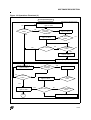
1
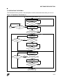
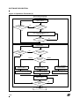
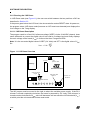
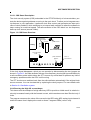
SAFE ST7
EVALUATION BOARD
(ST7FOPTIONS-EVAL)
USER MANUAL
June 2002
DOC- ST7FOPTIONS-EVAL
1
USE IN LIFE SUPPORT DEVICES OR SYSTEMS MUST BE EXPRESSLY AUTHORIZED.
STMicroelectronics PRODUCTS ARE NOT AUTHORIZED FOR USE AS CRITICAL COMPONENTS IN
LIFE SUPPORT DEVICES OR SYSTEMS WITHOUT THE EXPRESS WRITTEN APPROVAL OF
STMicroelectronics. As used herein:
1. Life support devices or systems are those
which (a) are intended for surgical implant into
the body, or (b) support or sustain life, and
whose failure to perform, when properly used in
accordance with instructions for use provided
with the product, can be reasonably expected
to result in significant injury to the user.
1
2. A critical component is any component of a life
support device or system whose failure to
perform can reasonably be expected to cause
the failure of the life support device or system,
or to affect its safety or effectiveness.
ST72F26x MCU FAMILY
SAFE ST7 EVALUATION BOARD USER MANUAL
1 INTRODUCTION
The objective of the Safe ST7 Evaluation Board is to allow you to try out all the special features embedded in the ST72F26x MCU family. You can learn how each feature works and
how to use them the best way by playing with the user controls and jumper settings. For example, you can check out what happens to your application when the voltage becomes erratic
or the clock signal suddenly fails.
Examples of what you can do:
■
Save application data in E2PROM when a power cut occurs and/or the main clock source
fails (using the AVD and CSS options). Prove it works by resuming the application exactly
where it left off after restoring the data saved by the AVD interrupt routine.
■
Drive LEDs directly (using the MCU’s high sink current I/O ports)
■
Experiment with different clock sources: external crystal or ceramic resonator, internal RC
oscillator, external clock signal. The advantages of the internal RC: less cost, less
components, less power consumption!
■
Check out the safe operation of the MCU in varying supply voltage conditions. You change
the voltage using a trimmer. The voltage level is displayed on a 3-digit display. The LVD will
automatically hold the MCU in reset state while the voltage is below the safe threshold. No
need for an external reset circuit so more savings in board space and components.
■
Select different power sources, on-board 9V battery or external power supply
■
■
Change E2PROM data or Flash program memory on-the-fly using In-Application
Programming (IAP)
Use Nested interrupts to let you interrupt an interrupt routine, service a higher priority
interrupt and resume the one previously being serviced.
This evaluation board incorporates basic input sources such as push-buttons, analog trimmer
or output sources (LEDs, 7-segment displays, buzzer) and a wire-wrap area so you can easily
develop your own application.
The following development tools can be ordered separately: assembler, linker, C compiler,
source level debugger, hardware emulator, programming boards and gang programmer.
For ordering information, see our website at http://mcu.st.com or contact your local sales
office.
June 2002
1/28
1
Table of Contents
1 INTRODUCTION . . . . . . . . . . . . . . . . . . . . . . . . . . . . . . . . . . . . . . . . . . . . . . . . . . . . . . 1
2 SAFE ST7 EVALUATION BOARD DESCRIPTION . . . . . . . . . . . . . . . . . . . . . . . . . . . 4
2.1 OVERVIEW . . . . . . . . . . . . . . . . . . . . . . . . . . . . . . . . . . . . . . . . . . . . . . . . . . . . . . 4
2.2 BOARD FEATURES . . . . . . . . . . . . . . . . . . . . . . . . . . . . . . . . . . . . . . . . . . . . . . 5
2.3 POWER SUPPLY . . . . . . . . . . . . . . . . . . . . . . . . . . . . . . . . . . . . . . . . . . . . . . . . . 6
2.4 OSCILLATION SYSTEM . . . . . . . . . . . . . . . . . . . . . . . . . . . . . . . . . . . . . . . . . . . 6
2.5 ICP (IN-CIRCUIT PROGRAMMING) CONNECTOR . . . . . . . . . . . . . . . . . . . . . . 7
2.6 I²C SERIAL COMMUNICATION . . . . . . . . . . . . . . . . . . . . . . . . . . . . . . . . . . . . . . 8
2.7 SPI SERIAL COMMUNICATION . . . . . . . . . . . . . . . . . . . . . . . . . . . . . . . . . . . . . 8
2.8 I/O PORT FUNCTIONALITY . . . . . . . . . . . . . . . . . . . . . . . . . . . . . . . . . . . . . . . . 9
2.8.1 Port A . . . . . . . . . . . . . . . . . . . . . . . . . . . . . . . . . . . . . . . . . . . . . . . . . . . . . . . . . . . . . 9
2.8.2 Port B . . . . . . . . . . . . . . . . . . . . . . . . . . . . . . . . . . . . . . . . . . . . . . . . . . . . . . . . . . . . . 9
2.8.3 Port C . . . . . . . . . . . . . . . . . . . . . . . . . . . . . . . . . . . . . . . . . . . . . . . . . . . . . . . . . . . . . 9
2.9 JUMPER DESCRIPTIONS . . . . . . . . . . . . . . . . . . . . . . . . . . . . . . . . . . . . . . . . . 10
2.9.1 W2 - Variable voltage enable/disable . . . . . . . . . . . . . . . . . . . . . . . . . . . . . . . . . . .
2.9.2 W3 - Board reference voltage selection . . . . . . . . . . . . . . . . . . . . . . . . . . . . . . . . . .
2.9.3 TP4 and TP5 - GND and VDD pins . . . . . . . . . . . . . . . . . . . . . . . . . . . . . . . . . . . . .
2.9.4 W6 - MCU power consumption . . . . . . . . . . . . . . . . . . . . . . . . . . . . . . . . . . . . . . . .
2.9.5 W4 and W5 - Source clock selection . . . . . . . . . . . . . . . . . . . . . . . . . . . . . . . . . . . .
2.9.6 W8 and W9 - External interrupts enable/disable . . . . . . . . . . . . . . . . . . . . . . . . . . .
2.9.7 W10 - Buzzer enable/disable . . . . . . . . . . . . . . . . . . . . . . . . . . . . . . . . . . . . . . . . . .
2.9.8 TP1, TP2 and TP3 - Port connectors . . . . . . . . . . . . . . . . . . . . . . . . . . . . . . . . . . . .
2.9.9 W15 - LEDs enable/disable . . . . . . . . . . . . . . . . . . . . . . . . . . . . . . . . . . . . . . . . . . .
2.9.10W13 and W14 - Analog inputs enable/disable . . . . . . . . . . . . . . . . . . . . . . . . . . . . .
2.9.11W12 - High Sink I/O test enable/disable . . . . . . . . . . . . . . . . . . . . . . . . . . . . . . . . .
2.9.12W16, W17 and W18 - 7 seg Displays enable/disable . . . . . . . . . . . . . . . . . . . . . . .
2.9.13W1 - ICP Connector . . . . . . . . . . . . . . . . . . . . . . . . . . . . . . . . . . . . . . . . . . . . . . . . .
2.9.14W7 - I²C connector . . . . . . . . . . . . . . . . . . . . . . . . . . . . . . . . . . . . . . . . . . . . . . . . . .
2.9.15JP11 - SPI Connector . . . . . . . . . . . . . . . . . . . . . . . . . . . . . . . . . . . . . . . . . . . . . . .
10
10
10
10
10
10
11
11
11
11
11
11
11
11
11
3 SOFTWARE DESCRIPTION . . . . . . . . . . . . . . . . . . . . . . . . . . . . . . . . . . . . . . . . . . . 12
3.1 OPTION BYTE CONFIGURATION . . . . . . . . . . . . . . . . . . . . . . . . . . . . . . . . . . 12
3.2 MAIN MCU INITIALIZATION ROUTINE . . . . . . . . . . . . . . . . . . . . . . . . . . . . . . 13
3.3 COUNTERS AND USE OF TIMING RESOURCES . . . . . . . . . . . . . . . . . . .28
. . . 13
3.4 INTERRUPT SERVICE ROUTINES . . . . . . . . . . . . . . . . . . . . . . . . . . . . . . . . . . 13
2/28
1
Introduction
3.5 MAIN PROGRAM ROUTINE . . . . . . . . . . . . . . . . . . . . . . . . . . . . . . . . . . . . . . . 13
3.6 OPERATING THE DEMOS . . . . . . . . . . . . . . . . . . . . . . . . . . . . . . . . . . . . . . . . 15
3.6.1 Running the LVD Demo . . . . . . . . . . . . . . . . . . . . . . . . . . . . . . . . . . . . . . . . . . . . . . 18
3.6.1.1LVD Demo Description . . . . . . . . . . . . . . . . . . . . . . . . . . . . . . . . . . . . . . . . . 18
3.6.2 Running the AVD Demo . . . . . . . . . . . . . . . . . . . . . . . . . . . . . . . . . . . . . . . . . . . . . . 19
3.6.2.1AVD Demo Description . . . . . . . . . . . . . . . . . . . . . . . . . . . . . . . . . . . . . . . . . 19
3.6.3 Running the CSS Demo . . . . . . . . . . . . . . . . . . . . . . . . . . . . . . . . . . . . . . . . . . . . . . 20
3.6.3.1CSS Demo Description . . . . . . . . . . . . . . . . . . . . . . . . . . . . . . . . . . . . . . . . . 21
3.6.4 Running the High I/O current demo . . . . . . . . . . . . . . . . . . . . . . . . . . . . . . . . . . . . . 21
3.6.4.1High Sink Demo Description . . . . . . . . . . . . . . . . . . . . . . . . . . . . . . . . . . . . . 22
3.6.5 Running the IAP demo . . . . . . . . . . . . . . . . . . . . . . . . . . . . . . . . . . . . . . . . . . . . . . . 22
3.6.5.1IAP Demo Description . . . . . . . . . . . . . . . . . . . . . . . . . . . . . . . . . . . . . . . . . . 23
3.6.6 Running the Nested & Concurrent Interrupts demo . . . . . . . . . . . . . . . . . . . . . . . . . 24
3.6.6.1Nested & Concurrent Interrupts Demo Description . . . . . . . . . . . . . . . . . . . . 25
4 APPENDIX 1: SAFE ST7 EVALUATION BOARD SCHEMATIC . . . . . . . . . . . . . . . . 26
3/28
Safe ST7 Evaluation Board DESCRIPTION
2 SAFE ST7 EVALUATION BOARD DESCRIPTION
The Safe ST7 Evaluation Board is designed to support any of the SDIP32 package devices
from the ST72F264 family (ST72F264, 262, 260).
2.1 OVERVIEW
This board is supplied ready-to-use, to let you try out all the functions described in this manual.
The board is delivered with a SDIP32 socket. You will have to build an adapter if you need
evaluate the ST72F264 in other packages. Additional hardware functions can be implemented
by installing components in the wire-wrap area as shown in Figure 1 below.
Figure 1. Safe ST7 Evaluation Board layout
Battery
ICP Connector
Reset
Button
Wire-Wrap
Area
MCU +
Clock system
PA, PB &
PC Ports
SPI
Connector
Three
7-segments
LEDs
I²C
Connector
Buzzer
Voltage
Trimmer
Output
LEDs
For more details, please refer to the schematic drawing in the appendix.
4/28
1
Two Push
Buttons
Safe ST7 Evaluation Board DESCRIPTION
The main Safe ST7 Evaluation Board components are:
- Socketed ST72F264
- 16MHz crystal
- Reset pushbutton
- ICP connector
- Socketed I²C 8K byte EEPROM (M24C08)
- Socketed SPI 4K byte EEPROM (M95040)
- 2 pushbuttons for external interrupts
- 22 pins for expansion ports
- Row of 8 LEDs for displaying binary values
- Three 7-segment LEDs
- High efficiency LED
- Potentiometer for main voltage variation
- Potentiometer for I/O current variation
- 9-volt battery
- Buzzer
- Wire-Wrap area
2.2 BOARD FEATURES
- Low voltage detector (3 levels programmable by option bytes)
- Auxiliary voltage detector
- Multi-Oscillator and Clock Security System
- High Sink/source current
- Nested/ Concurrent Interrupts
- In-Application Programming
- In-Circuit Programming
- I²C & SPI communications interfaces
- 10-bit ADC
5/28
Safe ST7 Evaluation Board DESCRIPTION
2.3 POWER SUPPLY
This board is supplied with a PP3 9-volt battery demonstrating the board’s low power consumption. A complementary DC power supply input (ref. J1) is provided to supply the board
by external ( 9 to 13 Volt) power. When using this power supply, take care to respect the polarities marked next to the two-pole connector.
Warning:
Disconnect the battery from its socket when the Safe ST7 Evaluation
Board is not in use.
The reference voltage on board (VDD) is selected through the W3 jumper. You can choose between two reference voltages, either a regulated 5 volts and or a voltage that varies, by
moving the R5 trimmer position, from 0 to 5.6 Volts as shown in Figure 2.
Figure 2. How to Change the Board Voltage Reference
5 regulated Volts selected
Variable Voltage selected
VDD Board
VDD Board
5 regulated Volts
W3
Variable Voltage
5 regulated Volts
W3
Variable Voltage
RV1
The 1N4004 diodes provide for polarity protection and the LD1 LED provides an indication that
power is being supplied to the board.
2.4 OSCILLATION SYSTEM
The board is designed to be used with an on-board 16-MHz crystal. This allows you to configure the CPU frequency up to 8 MHz.
The oscillator system is designed to fit a range of application needs, and you can choose between three different sources using the W4 and W5 jumpers as shown in Figure 3.
6/28
Safe ST7 Evaluation Board DESCRIPTION
Figure 3. How to Change the Oscillator Frequency Source
Crystal Resonator
Internal RC oscillator
External Clock
C4
C4
C4
W4
W4
W4
XT1
XT1
XT1
W5
W5
W5
C5
C5
C5
2.5 ICP (IN-CIRCUIT PROGRAMMING) CONNECTOR
You can use In Circuit Programming (ICP) to update the entire contents of the Flash memory
(including option bytes) using the ICC protocol. Figure 4 shows the connector pin assignment.
If you are connecting an ST Programming Tool to Safe ST7 Evaluation Board just connect
cable provided with the ST Programming Tool to the ICP connector "W2" and then power on
the board.
Figure 4. How to use the ICP Connector
Cable to ST Programming Tool
ICP Connector Pin assignment
ICCDATA
ICCCLK
RESET
VPP
OSC_CLK
ICP
2
1
W2
10
9
ICP
2
1
10
9
W2
7/28
Safe ST7 Evaluation Board DESCRIPTION
2.6 I²C SERIAL COMMUNICATION
An external 8 Kb EEPROM memory with an I²C serial interface is connected to the I²C pins of
the ST7 socket as shown in the following figure. The serial EEPROM may also be disconnected and the I²C bus used for other communications.
Figure 5. How to use the I²C Connection
Using the I²C BUS
SCLI
SDAI
ST7 I²C
pins
SCLI
SDAI
I2C
ST7 I²C
pins
I2C
Using the On-board I²C EEPROM
W7
M24C08
M24C08
W7
U4
U4
Install all the jumpers on the I²C connector.
Remove the jumpers and use left connector side.
2.7 SPI SERIAL COMMUNICATION
An external 4 Kb EEPROM memory with an SPI serial interface is connected to the SPI pins
of the ST7 socket as shown in the following figure. The serial EEPROM may also be disconnected and the SPI bus used for other communications.
Figure 6. How to use the SPI Connection
Using the SPI Bus
PB3
MOSI
MISO
SCK
SPI
ST7 I²C
pins
ST7 I²C
pins
PB3
MOSI
MISO
SCK
M95040
U5
U5
Install all the jumpers on the SPI connector.
8/28
W 11
M95040
W 11
SPI
Using the On-board SPI EEPROM
Remove the jumpers and use left connector side.
Safe ST7 Evaluation Board DESCRIPTION
2.8 I/O PORT FUNCTIONALITY
All I/O port pins are accessible through external connectors ( TP1 for port A, TP2 for port B
and TP3 for port C ).
2.8.1 Port A
The PA0 and PA1 pins are connected to the ICP connector using their alternate functions, ICCCLK and ICCDATA.
The PA2 and PA3 pins are used to enable the U6 and U7 7-segment LED displays (useful for
multiplexing).
The PA5 pin can be used to generate an external interrupt (ei0). It is connected to the ground
via the SW2 push-button switch .
The PA4 and PA6 pins alternate functions (SCLI and SDAI) are used for connecting an I²C
communication with the external I²C EEPROM.
PA7 is used to exercise the high sink I/O current capability through the High efficiency LED.
Table 1. Port A Alternate Functions
PA0
PA1
PA2
PA3
PA4
PA5
PA6
PA7
ICCCLK
ICCDATA
In Circuit Communication Clock
In Circuit Communication Data
SCLI
RDI
SDAI
TDO
I²C Clock
SCI output
I²C Data
SCI input
2.8.2 Port B
This port is connected simultaneously to 8 LEDs and to the three 7-segment displays. It can
be used to display 8 bits of binary data.
Table 2. Port B Alternate Functions
PB0
PB1
PB2
PB3
PB4
PB5
PB6
PB7
ICAP1_A
OCMP1_A
ICAP2_A
OCMP2_A
MOSI
MISO
SCK
SS
Timer A Input Capture 1
Timer A Output Compare 1
Timer A Input Capture 2
Timer A Output Compare 2
SPI Master Out Slave In Data
SPI Master In Slave Out Data
SPI Serial Clock
SPI Slave Select
2.8.3 Port C
The PC0 pin can be connected to ground via the SW3 push-button in order to generate an
external interrupt (ei1).
9/28
Safe ST7 Evaluation Board DESCRIPTION
The PC1/OCMP1_B pin can be connected to a buzzer through the W10 jumper .
The PC2 pin is used to enable the output signal to the LEDs. A high level on PC2 enables the
logic states programmed by port B to be output on the 8 LEDs.
The PC3 pin is used to enable the U8 7-segment LEDs display (useful for multiplexing).
The PC4/AIN4 pin can be used through the W14 jumper as in analog input to measure the
voltage level of R13.
The PC5/AIN5 pin can be used through the W13 jumper as in analog input to measure the
VREF voltage.
Table 3. Port C Alternate Functions
PC0
PC1
PC2
PC3
PC4
PC5
ICAP1_B / AIN0
OCMP1_B / AIN1
CLKOUT / AIN2
ICAP2_B / AIN3
OCMP2_B / AIN4
EXTCLK_A / AIN5
Timer B Input Capture 1
Timer B Output Compare 1
CPU Clock Out
Timer B Input Capture 1
Timer B Output Compare 1
Timer A External Clock
Analog Input 0
Analog Input 1
Analog Input 2
Analog Input 3
Analog Input 4
Analog Input 5
2.9 JUMPER DESCRIPTIONS
2.9.1 W2 - Variable voltage enable/disable
This jumper allows you to disable the variable voltage and thus reduce the total power consumption of the board and extend battery life.
2.9.2 W3 - Board reference voltage selection
Refer to Section 2.3 POWER SUPPLY.
2.9.3 TP4 and TP5 - GND and VDD pins
These spare ground and VDD pins are for test purposes or for providing power to components
in the wire-wrap area.
2.9.4 W6 - MCU power consumption
This jumper is only for connecting to the MCU power supply. Its main purpose is to allow you
to measure the current consumption of the µC by connecting a DC-ammeter in series.
2.9.5 W4 and W5 - Source clock selection
Please refer to Section 2.4 Oscillation system.
2.9.6 W8 and W9 - External interrupts enable/disable
Those two jumpers allow you to disconnect the two push-buttons SW2 and SW3 from the PA5
and PC0 pins respectively.
10/28
Safe ST7 Evaluation Board DESCRIPTION
2.9.7 W10 - Buzzer enable/disable
This jumper allows you to use the buzzer by connecting it to the PC1 pin.
2.9.8 TP1, TP2 and TP3 - Port connectors
These jumpers allow you to access all I/O ports.
2.9.9 W15 - LEDs enable/disable
This jumper is used to connect the LEDs to ground through the resistor network. It is recommended to remove the jumper from the board if this feature is not used.
2.9.10 W13 and W14 - Analog inputs enable/disable
These jumpers are for measuring the Vref analog voltage and the voltage through R13. Removing them will disable those two features (The measurement of the VDD voltage value and
the measurement of the current driven through the high efficiency LED).
2.9.11 W12 - High Sink I/O test enable/disable
This jumper lets you enable or disable the High efficiency LED.
2.9.12 W16, W17 and W18 - 7 seg Displays enable/disable
These jumpers allow you to enable/disable the three 7-seg displays (useful for multiplexing).
2.9.13 W1 - ICP Connector
Please refer to Section 2.5 ICP (In-Circuit Programming) connector.
2.9.14 W7 - I²C connector
Please refer to Section 2.6 I²C serial communication.
2.9.15 JP11 - SPI Connector
Please refer to Section 2.7 SPI serial communication.
11/28
SOFTWARE DESCRIPTION
3 SOFTWARE DESCRIPTION
This part gives a short description of the whole program as a main routine that uses many
other functions and several drivers. The configuration of the microcontroller and also the configuration of option bytes is described first, followed by an overview of the main program structure. Finally, we will provide a detailed description of how to use the board’s features.
3.1 OPTION BYTE CONFIGURATION
Option bytes are only accessed using In-Circuit Programming or an ST programming tool
such as an EPB. In this case, the option bytes are configured as described below.
– Watchdog is configured to be enabled by software and to allow the MCU to enter Halt Mode
(no reset on Halt).
– The LVD threshold is fixed to the medium value.
– Sector 0 size is 4 Kbytes.
– No program memory protection.
– Port C external interrupt mapping is configured as ei1.
– The clock security system is always on.
– Oscillator type is resonator oscillator.
– Oscillator range is between 8 and 16 MHz.
Table 4. Option byte configuration
OSC
OSC
TYPE1
0
WDGHALT
0
TYPE0
OSC
RNGE1
OSC
RNGE0
OFF
0
0
0
1
1
1
WDG SW
VD1
VD0
SEC1
SEC0
FMP R
FMP W
1
0
1
1
1
0
0
CSS
1
12/28
PLL
OSC
RNGE2
EXTIT
SOFTWARE DESCRIPTION
3.2 MAIN MCU INITIALIZATION ROUTINE
This routine initializes the MCU as follows:
– MISCR (miscellaneous register): external interrupts trigger on falling edge, no slow mode
and fCPU=8 MHz.
– Port A: PA7 (Driving the High efficiency LED) is an open drain output, PA6 & PA4 used by
I²C as input without interrupt, PA5 (Push-button) used as floating input with interrupt, PA2 &
PA3 (multiplexing 7-seg displays) as push-pull outputs.
– Port B: used as push pull output to display data.
– Port C: PC5 & PC4 as ADC alternate inputs, PC3 as push-pull output (multiplexing 7-seg
displays), PC2 to select the LED bank (push-pull output), PC1 to drive the buzzer and PC0
as an input with interrupt (push-button).
3.3 COUNTERS AND USE OF TIMING RESOURCES
– Timer A is used as a real time clock that provides a precise time base for all program routines. Timer A interrupt is enabled.
– Timer B is mainly used to drive the buzzer using PWM mode without interrupts.
3.4 INTERRUPT SERVICE ROUTINES
– Timer A interrupt: increment (circular buffer) several global counters used as time counters
when the free running counter reaches the calculated value.
– AVD interrupt: saves the current mode when the power drops and, if we are in AVD mode,
the last displayed digits are saved in the external I²C EEPROM using the I²C driver.
– ei1 Interrupt: this interrupt is used to wake-up the microcontroller from idle mode (HALT)
and also it increments a circular variable used by the main program to enter the corresponding test.
– ei0 Interrupt: this interrupt is used to test concurrent and nested interrupts.
3.5 MAIN PROGRAM ROUTINE
The main program includes the initialization code and an endless loop that processes the
pushbutton inputs. In fact, after initialization and enabling interrupts, the main program will
continue running in an infinite loop and wait for an external interrupt to switch to one of the
demo routines: (LVD, AVD/CSS, High Current I/O, IAP, Concurrent/ Nested Interrupts).
By default the program is in Halt mode (to reducing power consumption).
Warning:
Disconnect the battery from its socket when the Safe ST7 Evaluation
Board is not in use.
13/28
SOFTWARE DESCRIPTION
Figure 7. Main program flowchart
Begin
Disable all Interrupts
MCU Initialization
I²C Initialization
Init Timer A
Safety procedure
This function is used for the AVD interrupt
Disable RASS Keys
Enter Halt Mode
Enable all interrupts
: Program path/ PGM interrupt
“START” message
“FINISH” message
LVD Demo
Nested IT Demo
Test “MODE”
variable
Concurrent IT Demo
AVD Demo
High Current Demo
14/28
IAP Demo
SOFTWARE DESCRIPTION
3.6 OPERATING THE DEMOS
The flowcharts below provide a full description of all the tests and demos that you can run.
Figure 8. Operations Flowchart (1)
Power-on the board / RESET
HALT Mode
MCU in a HALT state
Push The PGM
button
No
No
Yes
End
Push The PGM
button
Display “START “
Light-on LED 0
Push The PGM
button
No
Yes
No
Push The PGM
button
LowLoL
Voltage Detector Demo
f
Display " LVD "
Light-on LED 1
No
Push the DEMO
button
Yes
Yes
Display the VDD voltage
Light-on LED1
No
Push The PGM
button
Yes
No
Push The PGM
button
AVD and CSS Demo
Display "AVD CSS "
Light-on LED 2
No
Push the DEMO
button
Yes
Yes
Display a counter 000..999
Light-on LED2
Push The PGM
button
No
Yes
To next figure
15/28
SOFTWARE DESCRIPTION
Figure 9. Operations Flowchart (2)
From previous Figure
High I/O Current Demo
Display "HIO"
Light-on LED 3
No
No
Push The PGM
button
Push the DEMO
button
Yes
Yes
Display the current inside the High Efficiency LED
Light-on the high efficiency Led
Light-on LED 3
No
Push The PGM
button
Yes
In-Application Programming Demo
Display "IAP"
Light-on LED 4
No
No
Push The PGM
button
Push the MODE
Button
Yes
Score 0
Test XFlash
memory
Score 1
First Time
Display "SCORE 1"
Light-on LED 4
Receive & Re-program
Score1 from the SPI E²PROM
Display "SCORE 0"
Light-on LED 4
Display "TRANSFER"
Light-on LED 4
Send Score0 & Score1
Receive & Re-program
to the SPI E²PROM
Score0 from the SPI E²PROM
Display " DONE "
Light-on LED 4
Push The PGM
button
Yes
To next Figure
16/28
No
SOFTWARE DESCRIPTION
Figure 10. Operations Flowchart (3)
From previous Figure
Concurrent Interrupts Demo
Display " CONCURRENT IT "
Light-on LED 5
No
No
Push The PGM
button
End of the
message
Light-on LED 5
Yes
Yes
Play music Score
Light-on LED 5
Push The PGM
button
IT1
No
Yes
No
Push The DEMO
button
End of The Score
IT0
Yes
Wait End of score
Light-on LED 5
Display a lighting Sequence on LEDs
Nested Interrupts Demo
Display " NESTED IT "
Light-on LED 6
Yes
End of the
message
Light-on LED 6
No
No
Push The PGM
button
Play music Score
Light-on LED 6
Push The PGM
button
Yes
Display " FINISH "
Light-on LED 7
Yes
End of The Score
No
Push The DEMO
button
Yes
End
Display a lighting Sequence on LEDs
17/28
SOFTWARE DESCRIPTION
3.6.1 Running the LVD Demo
In LVD Demo state (see Figure 11), the user can switch between the two positions of W3 as
described in Section 2.3.
If the power goes below the LVD level, the microcontroller enters RESET state. At power-on,
the program enters LVD demo mode (because an LVD reset was detected) and displays the
VDD voltage on the 7-seg display.
3.6.1.1 LVD Demo Description
The program reads in a fixed 2.4V reference voltage (VREF) via the 10-bit ADC channel, does
some arithmetic to convert the digital value it has read to a voltage level and finally displays
the main voltage of the board (VDD) in Volts on the three 7-segment LEDs.
Note: X is the converted digital value of VREF (2.4 Volts) and 3FF is the digital value of VDD,
So:
3FF
V DD = 2.4 × ----------X
Figure 11. LVD Demo Overview
ST72F264
press to reset
Battery
SAFE ST7
EVALUATION BOARD
move the jumper
to right
off
press until LED1
lights-on
on
Push to run
the Demo
Potentiometer
LED1
The W3 jumper must be moved to the right to select the variable power supply. If the RV1
trimmer is turned completely clockwise, the board is powered by 5.6 Volts. If the trimmer is
turned counter-clockwise the VDD value will decrease until we reach the LVD threshold (VIT-),
at which point the microcontroller enters reset mode.
18/28
SOFTWARE DESCRIPTION
In power-on, if the trimmer is turned clockwise, the device will leave reset state and we can
see the VIT+ threshold on the display.
Note: the VIT- reference value for a voltage drop is lower than the VIT+ reference value for
power-on in order to avoid parasitic reset when the microcontroller starts running and sinks
current on the supply (hysteresis).
3.6.2 Running the AVD Demo
In Auxiliary Voltage Detector & Clock Security System Demo state (see Figure 12), the 7-seg
display shows a counter that increments from 000 to 999.
To test the AVD capability:
– Disconnect the battery or decrease the VDD voltage using the power trimmer until the MCU
enters RESET state.
– Then, supply the board with the right voltage.
– You will see that the counter does not restart at 000, but resumes counting from the last displayed value before shut-down.
3.6.2.1 AVD Demo Description
For system integrity management, in addition to the LVD feature, the Safe ST7 Evaluation
Board has an auxiliary voltage detector (AVD) with interrupt capability. In case of a drop in
voltage, the AVD interrupt acts as an early warning, allowing software to shut down safely before the LVD resets the microcontroller. The AVD works closely with the LVD and functions
only if the LVD is enabled through option byte (see “Option byte configuration” on page 12).
19/28
SOFTWARE DESCRIPTION
Figure 12. AVD Demo Overview
Disconnect the battery
press to reset
ST72F264
Battery
ST72F264
press to reset
Battery
SAFE ST7
EVALUATION BOARD
SAFE ST7
EVALUATION BOARD
move the jumper
to right
off
move the jumper
to left
on
press until LED2
lights-on
Push to
run the Demo
press until LED2
Push to
lights-on
run the Demo
Potentiometer
LED2
LED2
In case of power drop, and before going into reset state, the AVD interrupt will save the last
displayed value in the external EEPROM (M24C08) using the I²C protocol. On power-on, the
software checks if the last reset was made by the LVD, if this is the case, it downloads the previously saved value from the external EEPROM to RAM memory in order to resume counting
as normal.
To cause a voltage drop, we can choose between two solutions as shown in the Figure 12.The
first method consists of moving the W3 jumper to the right, then decreasing the main voltage
by turning the RV1 trimmer counter-clockwise. The second method consists of moving the W3
jumper to the left so that we will have a 5-Volt reference value, and then disconnecting the battery.
3.6.3 Running the CSS Demo
To run this demo, we have to be in the same state as in the AVD demo see “Running the AVD
Demo” on page 19.
Once the main program runs at 8 MHz, Timer A is configured to manage the counting operation displayed on the three 7-segments LEDs.
To test the CSS capability:
– Disconnect the oscillator by removing the W4 and W5 jumpers.
– You will see the frequency decreases significantly but that the counter still working.
20/28
SOFTWARE DESCRIPTION
3.6.3.1 CSS Demo Description
The clock security system (CSS) embedded in the ST72F264 family of microcontrollers, protects the device against problems occurring to the main clock. To allow you to integrate security features in your application, it performs clock filter control and generates an interrupt in
case of clock problems, while switching to an internal safe oscillator to allow the software to
keep running at a reduced speed. The safe oscillator of the CSS block is a low frequency
back-up clock source (around 3 Mhz).
Figure 13. CSS Demo Overview
Disconnect the
two clock jumpers
ST72F264
press to reset
Battery
SAFE ST7
EVALUATION BOARD
move the jumper
to left
press until LED2
lights-on
Push to
run the Demo
LED2
If the clock signal disappears, which you can provoke by disconnecting the two jumpers as
shown in Figure 13, the safe oscillator delivers a low frequency clock signal (around 3MHz) for
a safe oscillator period which allows the ST7 to save any critical data or perform any kind of
emergency operations while the CPU is still running.
The ST7 clock source switches back from the safe oscillator automatically if the original clock
source recovers. You can simulate this by replacing the clock jumpers. For more details refer
to Section 2.4 Oscillation system.
3.6.4 Running the High I/O current demo
This demo uses the example of a high efficiency LED to provide a visible result: its relative luminosity increases linearly with the forward current, which reaches more than 50mA at only 3
Volts.
The program measures the value of the current in the LED using ADC analog input channel 4
and at the same time it displays the result on three 7-segment LEDs (units in mA).
21/28
SOFTWARE DESCRIPTION
To vary the forward current, we have to move the RV2 trimmer position as shown in Figure 14
You can verify the current value for yourself by connecting a serial ammeter to W12.
Figure 14. High Sink I/O Demo Overview
ST72F264
press to reset
Battery
SAFE ST7
EVALUATION BOARD
move the jumper
to left
-
+
press until LED3
lights-on
Push to
run the Demo
LED3
3.6.4.1 High Sink Demo Description
This demo shows how the high sink outputs can be used and how to measure the current delivered by any of the high sink outputs on Port A. In addition to standard I/O ports which sink
and sources a maximum (absolute rating) output current of 25mA, most ST7s include High
sink I/Os that can sink a current (absolute rating) output of up to 50mA. This allows you to
drive any type of high power device directly without needing expensive external circuitry.
3.6.5 Running the IAP demo
This demo consists of re-programming XFLASH sector 1 using the In-Application Programming. To show this, it reprograms one piece of music (64 Bytes) by another one using the SPI
communication protocol with the external M95040 4Kb SPI EEPROM memory.
The demo software includes an IAP_driver that will be copied to the RAM area to execute the
demo. It programs 16 bytes at a time.
For more details about XFLASH In-Application Programming refer to the ST7 FLASH Programming Reference manual.
As shown in Figure 15, you enter the IAP demo by pushing down the PGM button until LED4
lights-up and the “IAP” message appears. Then you must push the DEMO button. During this
time the device will be updated and when this is finished a “DONE” message will appear.
22/28
SOFTWARE DESCRIPTION
Note: If you don’t want to enter this mode, you must push the PGM button again to jump directly to the next demo.
Note: This demo only runs the software that downloads the musical sequence from the external EEPROM to the XFLASH device. This music data can be output on the buzzer. In order
to listen to the music and verify that the data has been changed by IAP, you have to run the
nested & concurrent interrupts demos.
Figure 15. IAP Demo Overview
ST72F264
press to reset
Battery
SAFE ST7
EVALUATION BOARD
keep the jumper
to left
press until LED4
lights-on
Push to run the Demo
LED4
3.6.5.1 IAP Demo Description
The ST72F26x microcontroller family has a single voltage extended Flash (XFLASH) area that
can be electrically erased and programmed either on a byte-by-byte basis or up to 32 bytes in
parallel. In-Application Programming (IAP) allows you to update program memory contents
when the device is already plugged on the application board, at minimum cost in terms of
added components and board area impact.
This programming mode uses an IAP driver program which has been previously programmed
in sector 0. This method is fully controlled by user software. This allows it to be adapted to the
user application (user-defined strategy for entering programming mode, choice of communications protocol used to fetch the data to be stored).
RAM Mapping
0xA0 to 0xA1: XFLASH start address (2 bytes)
0xA2 to 0xB2: 16-byte RAM buffer.
23/28
SOFTWARE DESCRIPTION
0xB2 to 0xCE: IAP_driver storage area, (used only while the demo is running)
Sector1 Mapping (Reprogrammable Area)
0xE000 to 0xE00F: 16 spare bytes for testing
0xE010 to 0xE04F: (64 bytes) Music score1 (Software reprogrammable bytes)
0xE050 to 0xE08F: (64 bytes) Music score 2
0xE090 to 0xE14F: All other constants
Figure 16. IAP Demo flowchart
Begin
Else 0xE010..0xE04F contents Score0 (or 1)
First time the chip is plugged in
Test 0xE000
content
Display "SCORE0" (or "SCORE1")
Display "TRANSFER"
Init SPI
Init SPI
Repeat 4 times
Send Score1&2 to M95040
Receive next 16 bytes of Score1 (2) from M95040
SPI Disable
Program 16 bytes of Score1 (2) to the right addresses
SPI Disable
Using IAP write "1" to 0xE000
Using IAP write "2" (1) to 0xE000
End
3.6.6 Running the Nested & Concurrent Interrupts demo
Most ST7 microcontrollers have two different interrupt management modes. The first is called
concurrent mode and does not allow an interrupt to be interrupted, unlike the nested mode
where a software priority is given to each interrupt.
24/28
SOFTWARE DESCRIPTION
3.6.6.1 Nested & Concurrent Interrupts Demo Description
Figure 17. Interrupts Demo Overview
ST72F264
press to reset
Battery
press to reset
ST72F264
Battery
SAFE ST7
EVALUATION BOARD
keep the jumper
to left
(2) Press to run IT0
Buzzer
SAFE ST7
EVALUATION BOARD
keep the jumper
to left
(2) Press to run IT0
(1) Press to run IT1
LED5
Concurrent Interrupt Demo
Buzzer
(1) Press to run IT1
LED6
Nested Interrupt Demo
As shown in Figure 17 this demo is divided into two parts: The first one runs concurrent interrupts while the second uses nested interrupts.
The IT0 and IT1 interrupt service routines are assigned to external interrupt vectors ei0 and
ei1. You can trigger the interrupts directly by pressing the two push-buttons shown in Figure
17:
IT1: outputs a piece of music (previously downloaded in the IAP demo) on the buzzer.
IT0: displays a lighting sequence on LEDs.
In the first demo (Concurrent Interrupts), all the interrupts have the same priority level, so the
interrupt with the highest hardware priority will be serviced (in this case it is ei0).
In this demo, you have to push the PGM button in order to trigger the IT1 routine, then pushing
the DEMO button, IT0 won’t interrupt the IT1 routine and you have to wait for the end of music
before the LEDs light up in sequence.
To run the nested interrupt demo the board must be in the state shown in Figure 17, then if you
push the PGM button, it will trigger the IT1 interrupt routine (music output). Before the end of
the music you have to push the DEMO button in order abort the IT1 routine and service the IT0
routine. When the program returns from IT0, it resumes playing the music from the point
where it was interrupted.
25/28
Appendix 1: Safe ST7 Evaluation Board SCHEMATIC
4 APPENDIX 1: SAFE ST7 EVALUATION BOARD SCHEMATIC
VCC
TP1
CD2
100nF
PA0
PA1
PA2
PA3
PA4
PA5
PA6
PA7
R2
4.7k
C2
100µF
LD1
U1
L7805
D1
1
TP2
V
OUT
GND
3
PB0
PB1
PB2
PB3
PB4
PB5
PB6
PB7
POWER
2
1N4004
V
IN
D2
1N4004
1
2
R1
470
CD1
C1
J1
100nF
100µF
1
2
3
4
5
6
7
8
1
2
3
4
5
6
7
8
VREF
TP3
BT1
PC0
PC1
PC2
PC3
PC4
PC5
Z1
2V4
W2
VCC
1
2
3
4
5
6
TP4
R4
1
2
8
1k
U2A
3
1
2
W3
VCC
1
2
3
4
RV1
10k
R5
4.7k
Z2
5V6
26/28
VCC
T1
2N2222
TS912
POWER SELECT
TP5
1
2
GND
Appendix 1: Safe ST7 Evaluation Board SCHEMATIC
VCC
VCC
8
R9
27k
R10
27k
VCC
D
2
SPI
Q
6
U4
3
W
R11
PA4
PA6
1
3
100
M95040
2
4
5
E0
E1
E2
SCLK
1
2
3
CD7
100pF
SDA
I2C
CD8
100pF
WC
7
M24C08
4
4
6
W7
100
R12
7
HOLD
C
VCC
SS
5
VSS
PB6
2
4
6
8
VSS
1
3
5
7
PB5
VCC
1
W11
PB4
8
U5
PB3
ICCDATA
PA1
W1
PA0
ICCCLK
2
4
6
8
10
RESET
R3
10k
VPP
VPP
1
3
5
7
9
VCC
ICP
OSC1
VCC
R6
4.7k
2
SW1
RESET
W6 IDD
U3
1
3
CD3
100nF
PB7
4
PB6
5
PB5
6
PB4
7
8
W4
W5
1
2
3
9
1
2
3
XT1
4Mhz
C4
22pF
C5
22pF
PB3
10
PB2
11
PB1
12
PB0
13
PC5
14
PC4
15
PC3 16
PC3
RESET
VDD
OSC1
VSS
OSC2
VPP/TEST
PB7/ SS
ICCCLK/PA0
PB6/SCK
ICCDATA/PA1
PB5/MISO
PA2
PB4/MOSI
PA3
NC
NC
NC
NC
PB3/OCMP2_A
SCLI/PA4
PB2/ICAP2_A
RDI/PA5
PB1/OCMP1_A
SDAI/PA6
PB0/ICAP1_A
TDO/PA7(HS)
PC5/EXTCLK_A/AIN5
AIN0/ICAP1_B/PC0
PC4/OCMP2_B/AIN4
AIN1/OCMP1_B/PC1
PC3/ICAP2_B/AIN3
AIN2/MCO/PC2
CD4
32
100nF
31
30
VCC
VCC
VCC
C3
R7
4.7k
100pF
R8
4.7k
VPP
29 PA0
ICCCLK
28 PA1
SW2
DEMO
ICCDATA
27 PA2
SW3
PGM
CD5
100nF
CD6
100nF
PA2
26 PA3
PA3
25
EI0
EI1
24
23
PA4
22
PA5
21
PA6
20
PA7
W8
19
PC0
18
PC1
17
PC2
W9
BZ1
W10
PC2
Buzzer
ST72F264
W12
W13
VREF
LD3
W14
LD4
LD6
PB3
Leds enable
LD9
R14
BC547
4.7k
T2
U7
7
6
4
2
1
10
9
5
PB0
PB1
PB2
PB3
PB4
PB5
PB6
PB7
U8
7
6
4
2
1
10
9
5
PB0
PB1
PB2
PB3
PB4
PB5
PB6
PB7
7
6
4
2
1
10
9
5
R16
1k
PA2
W16
R15
4.7k
T3
BC547
8
LD10
3
PB7
U6
PB0
PB1
PB2
PB3
PB4
PB5
PB6
PB7
1k
LD8
PC2
PB6
W15
1
3
PB5
LD7
LD2
8
PB4
I/O Test
RS1
2
3
4
5
6
7
8
9
LD5
PB2
3
PB1
RV2
R13
10
8
PB0
VCC
R18
1k
PA3
W17
R17
4.7k
T4
BC547
R20
1k
PC3
W18
R19
4.7k
T5
BC547
27/28
Appendix 1: Safe ST7 Evaluation Board SCHEMATIC
THE SOFTWARE INCLUDED IN THIS NOTE IS FOR GUIDANCE ONLY.
STMICROELECTRONICS SHALL NOT BE HELD LIABLE FOR ANY DIRECT, INDIRECT OR
CONSEQUENTIAL DAMAGES WITH RESPECT TO ANY CLAIMS ARISING FROM USE OF
THE SOFTWARE.
Information furnished is believed to be accurate and reliable. However, STMicroelectronics assumes no responsibility for the consequences
of use of such information nor for any infringement of patents or other rights of third parties which may result from its use. No license is granted
by implication or otherwise under any patent or patent rights of STMicroelectronics. Specifications mentioned in this publication are subject
to change without notice. This publication supersedes and replaces all information previously supplied. STMicroelectronics products are not
authorized for use as critical components in life support devices or systems without the express written approval of STMicroelectronics.
The ST logo is a registered trademark of STMicroelectronics
ã2002 STMicroelectronics - All Rights Reserved.
Purchase of I2C Components by STMicroelectronics conveys a license under the Philips I2C Patent. Rights to use these components in an
I2C system is granted provided that the system conforms to the I2C Standard Specification as defined by Philips.
STMicroelectronics Group of Companies
Australia - Brazil - Canada - China - Finland - France - Germany - Hong Kong - India - Israel - Italy - Japan
Malaysia - Malta - Morocco - Singapore - Spain - Sweden - Switzerland - United Kingdom - U.S.A.
http://www.st.com
28/28