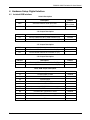
1
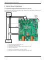
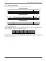
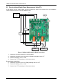
78M6610+LMU Evaluation Kit User Manual July 2013 Rev. 1 Maxim Integrated cannot assume responsibility for use of any circuitry other than circuitry entirely embodied in a Maxim Integrated product. No circuit patent licenses are implied. Maxim Integrated reserves the right to change the circuitry and specifications without notice at any time. Maxim Integrated 160 Rio Robles, San Jose, CA 95134 USA 1-408-601-1000 © 2013 Maxim Integrated Products, Inc. Maxim Integrated and the Maxim Integrated logo are trademarks of Maxim Integrated Products, Inc. 78M6610+LMU Evaluation Kit User Manual Table of Contents 1 Introduction ......................................................................................................................................... 4 1.1 Ordering Information .................................................................................................................. 4 1.2 Package Contents...................................................................................................................... 4 1.3 System Requirements ............................................................................................................... 4 1.4 Safety and ESD Notes ............................................................................................................... 5 1.5 Testing the 78M6610+LMU EV Board Prior to Shipping ........................................................... 5 2 USB Driver Installation ....................................................................................................................... 6 2.1.1 Confirm COM Port Mapping ............................................................................................. 6 2.1.2 FTDI COM Port Trouble Shooting.................................................................................... 6 3 Hardware Setup: Sensor Interface .................................................................................................... 7 3.1 Single-Phase Measurements using Shunts ............................................................................... 7 3.1.1 Jumper and Switch Descriptions...................................................................................... 8 3.1.2 Device Configuration ........................................................................................................ 8 3.2 Single/Multiphase Measurements Using CTs ............................................................................ 9 3.2.1 Jumper Position Changes .............................................................................................. 10 3.2.2 Device Configuration ...................................................................................................... 10 3.3 Pseudo-Isolated Single-Phase Measurements Using CTs...................................................... 21 3.3.1 Jumper Position Changes .............................................................................................. 23 3.3.2 Device Configuration ...................................................................................................... 23 4 Hardware Setup: Digital Interface.................................................................................................... 11 4.1 USB Interface........................................................................................................................... 11 4.2 RS-485 Interface ...................................................................................................................... 12 5 Graphical User Interface (GUI) ......................................................................................................... 13 5.1 GUI Initialization ....................................................................................................................... 13 5.1.1 SSI Tab .......................................................................................................................... 13 5.1.2 Device Tab ..................................................................................................................... 14 5.1.3 Direct Tab....................................................................................................................... 14 5.1.4 Configuration Tab........................................................................................................... 15 5.1.5 Command Register Tab ................................................................................................. 15 5.1.6 Calibration Tab ............................................................................................................... 16 5.1.7 Power Tab ...................................................................................................................... 16 5.1.8 Energy Tab..................................................................................................................... 17 5.1.9 Fundamental Tab ........................................................................................................... 17 5.1.10 Min/Max Tab ................................................................................................................. 17 5.1.11 Alarms Tab ................................................................................................................... 18 5.1.12 Monitor Tab,.................................................................................................................. 19 6 Hardware Design Information .......................................................................................................... 24 6.1 Board Schematics .................................................................................................................... 24 6.2 Bill of Materials......................................................................................................................... 28 6.3 PCB Layout .............................................................................................................................. 30 7 Contact Information .......................................................................................................................... 32 Revision History ........................................................................................................................................ 32 2 Rev 1 78M6610+LMU Evaluation Kit User Manual Figures Figure 1: 78M6610+LMU Evaluation Board Connections ..................................................................................... 7 Figure 2: 78M6610+LMU Evaluation Board Connections ..................................................................................... 9 Figure 2: 78M6610+LMU Evaluation Board Connections ................................................................................... 22 Figure 3: 78M6610+LMU Evaluation Board Electrical Schematic (1 of 4) .......................................................... 24 Figure 4: 78M6610+LMU Evaluation Board Electrical Schematic (2 of 4) .......................................................... 25 Figure 5: 78M6610+LMU Evaluation Board Electrical Schematic (3 of 4) .......................................................... 26 Figure 6: 78M6610+LMU Evaluation Board Electrical Schematic (4 of 4) .......................................................... 27 Figure 7: 78M6610+LMU Evaluation Board PCB Top View ............................................................................... 30 Figure 8: 78M6610+LMU Evaluation Board PCB Bottom View .......................................................................... 31 Rev 1 3 78M6610+LMU Evaluation Kit User Manual 1 Introduction The 78M6610+LMU evaluation kit (EV kit) demonstrates the capability of the 78M6610+LMU for monitoring a single-phase or split-phase AC load using up to two voltages and two currents (sensors included). The EV kit connects to a PC through a USB cable that provides both power and data communication to the board. A Windows®-based graphical user interface (GUI) communicates with the device over a virtual for simplified access to measurement data and controls. 1.1 Ordering Information PART 78M6610+LMUEVK1# TYPE Evaluation Kit #Denotes a RoHS-compliant device that may include lead that is exempt under the RoHS requirements. 1.2 Package Contents The 78M6610+LMU EV kit includes the following: • • • • • 78M6610+LMU Evaluation Board Two 20A Current Transformers USB Cable Assembly USB A-B 28/24 1.8M (Tyco/Amp 1487588-3) CD with Documentation, GUI Application, and USB Drivers Calibration Coefficients Document (Hardcopy Only) 1.3 System Requirements In addition to an AC source and load for measuring, the EV kit requires a Windows PC with the following features: • • 1GHz processor and 1GB RAM Minimum 1024 x 768 video display resolution • • Available USB port Microsoft Windows 7 or Windows XP® Windows and Windows XP are registered trademarks of Microsoft Corp. 4 Rev 1 78M6610+LMU Evaluation Kit User Manual 1.4 Safety and ESD Notes EXERCISE CAUTION WHEN LIVE AC VOLTAGES ARE PRESENT! Do not connect test equipment or external development boards directly to the nonisolated portion of the 78M6610 hardware. Damage to the 78M6610 and external equipment will occur due to the 78M6610’s “high side” reference topology. The 78M6610’s V3P3 supply (i.e., “high side”) is connected directly to Neutral (Earth Ground) creating a ground reference disparity with any properly grounded external equipment. The board components and firmware settings are designed to operate with the following nominal AC electrical ranges: Voltage Current Line Frequency 10-300 VAC 10 mA – 20A 46-64 Hz 1.5 Testing the 78M6610+LMU EV Board Prior to Shipping Before every kit is shipped, the board (and sensors) undergo a single-load point calibration using precise energy source equipment. The device temperature is also calibrated at the same time. Results printed out on paper and included with the EV kit. Rev 1 5 78M6610+LMU Evaluation Kit User Manual 2 USB Driver Installation This EV kit includes an isolated USB interface for serial communications with a PC. The FTDI USB controller IC FT2232 performs the USB functions. The FTDI Windows driver presents a virtual COM port for enabling serial communications. The FTDI Windows driver is a certified driver for Windows XP and Windows 7. Upon attaching the 78M6610+LMU EV Board to the PC, the Found New Hardware Wizard automatically launches and installs the appropriate driver files. If your PC does not find the FTDI driver files on its local hard disk drive, locate and reference the FTDI USB Driver and Utilities subdirectory on the CD. The FT2232 controller and 78M6610+LMU is powered from the USB cable and is active when no AC power is applied to the sensor interface of the 78M6610+LMU EV Kit. Note: If an older FTDI driver has been previously installed, it is recommended to remove the older version before installing this newer FTDI driver. Execute the ftdiClean.exe utility from the FTDI USB Driver and Utilities subdirectory. For FTDI driver support on other operating systems, refer to the FTDI website at www.ftdichip.com. 2.1.1 Confirm COM Port Mapping • Launch the Control Panel and click on the System icon. • The System Properties screen appears. Click on the Hardware tab. Click on Device Manager. Under Ports (COM & LPT), look for the USB Serial Port assignment. • Take note of the COM port assignment for the USB Serial Port. Two sequential COM ports are associated with the kit. Use the second COM port Port numbers may differ on each PC. 2.1.2 FTDI COM Port Trouble Shooting If the FTDI device driver did not install properly, there would be no assigned COM port number for the FTDI controller. Repeat the USB Driver Installation, see Section 2.1. Microsoft Windows may associate a Ball Point device to the FTDI USB controller. When this occurs a FTDI device COM port assignment is available via HyperTerminal but there is no communications data. Verify if a Ball Point device has been added to the “Human Interface Devices” via the Device manager. See Section 2.1.1 for access to the Device Manager. If a Ball Point device exists, delete it and unplug and replug the EV Kit’s USB cable. 6 Rev 1 78M6610+LMU Evaluation Kit User Manual 3 Hardware Setup: Sensor Interface The 78M6610+LMU EV board can be provisioned in multiple configurations. This manual covers common setups for using a shunt, shunt with CT, or two CTs. The board is provisioned and calibrated for the following configuration to retrieve the gain value of the shunt (printed on a label located on the bottom of the board). 3.1 Simple 2-Wire Single-Phase Measurements Using Shunts AC source Line Connect USB port to PC Neutral Load Figure 1: 78M6610+LMU Evaluation Board Connections 1. Connect the AC source Neutral output to J15. 2. Connect J8 to Load’s Neutral input. 3. Connect the AC source Line 1 output to J2 and to Load’s Line 1 input. Rev 1 7 78M6610+LMU Evaluation Kit User Manual 3.1.1 Jumper and Switch Descriptions The following tables describe the default position of the EV board jumpers and switches for using the on-board shunt current sensor at sensor slot S1. J23 Jumper Description J23 Pins Description Jumper 1/2 Connect J15 SHUNT to 78M6610+LMU Sensor Slot 1 Installed 2/3 Connect J10 CT2+ to 78M6610+LMU Sensor Slot 1 - J24 Jumper Description J24 Pins Description Jumper 1/2 Connects J8 SHUNT to 78M6610+LMU Sensor Slot 1 Installed 2/3 Connects J10 CT2- to 78M6610+LMU Sensor Slot 1 - J9 Jumper Description 3.1.2 J9 Pins Description Jumper 1/2 Connect AC Neutral to V3P3A (chip reference) Installed Device Configuration Use the Configuration tab to map the sensors as shown in the table below. Re-enter the gain value, as needed, for the shunt resistor into the S1_GAIN register. VA VB VC 8 Voltage S0 0 IA IB Pre-Amp Current S1 0 1X S1 Rev 1 78M6610+LMU Evaluation Kit User Manual 3.2 Single/Multiphase Measurements Using CTs In this diagram, the on-board relays are also wired in series to demonstrate load control. Line 1 Connect USB port to PC Neutral AC source Line 2 CT2 + + CT1 L1 N Line 1 Load L2 N Line 2 Load Figure 2: 78M6610+LMU Evaluation Board Connections 1. 2. 3. 4. 5. 6. 7. Rev 1 Connect the AC source Neutral to J15 and the load(s). Connect the AC source Line 1 to J2 and to J19 (Relay1) through the Line 1 CT. Connect J20 (Relay1) to Line 1 load. Connect Line 1 CT’s secondary to J14 (burden resistor). Connect the AC source Line 2 to J4 and to J31 (Relay2) through the Line 2 CT. Connect J30 (Relay1) to Line 1 load. Connect Line 2 CT’s secondary to J10 (burden resistor). 9 78M6610+LMU Evaluation Kit User Manual 3.2.1 Jumper Position Changes Move J23 and J24 jumpers to position CT to use CT2 for sensor slot S1. J23 Jumper Description J23 Pins Description Jumper 1/2 Connect J15 SHUNT to 78M6610+LMU Sensor Slot 1 - 2/3 Connect J10 CT2+ to 78M6610+LMU Sensor Slot 1 Installed J24 Jumper Description J24 Pins Description Jumper 1/2 Connects J8 SHUNT to 78M6610+LMU Sensor Slot 1 - 2/3 Connects J10 CT2- to 78M6610+LMU Sensor Slot 1 Installed J9 Jumper Description 3.2.2 J9 Pins Description Jumper 1/2 Connect AC Neutral to V3P3A (chip reference) Installed Device Configuration Use the Configuration tab to map the sensors as shown in the table below. Re-enter the gain value as needed for CT2 into the S1_GAIN register. VA VB VC Voltage S0 0 S0 S2 -S2 IA IB Pre-Amp Current S1 0 1X S1 0 S3 1X S3 Note: The values for VC will not be displayed correctly on the Power tab of the provided GUI due to the increased full-scale value of VC. Reported results for measurements derived from VC will be one-half the expected magnitude. 10 Rev 1 78M6610+LMU Evaluation Kit User Manual 4 Hardware Setup: Digital Interface 4.1 Isolated USB Interface Switch Description Description Default SW4 Sets host interface mode upon reset IFC0 Open IFC1 Closed SW5 Sets device address upon reset (UART/I2C modes) Both Closed J12 Jumper Description J12 Pins Description Default 1/2 Connect 78M6610+LMU to USB Controller (U3) Installed 2/3 Connect 78M6610+LMU to RS485 transceiver (U11) - J17 Jumper Description J17 Pins Description Default 1/2 Connect USB Controller to isolation IC (U7) Installed 2/3 Connect RS485 transceiver to isolation IC (U7) - J18 Jumper Description J18 Pins Description Default 1/2 Connect USB Controller to isolation IC (U7) Installed 2/3 Connect RS485 transceiver to isolation IC (U7) - J24A, J24B Jumper Description Rev 1 J24A/B Pins Description Default 1/1 Connects MP0 to LED4 Installed 2/2 SDO/TXD/SDAo - 3/3 SDI/RXD/SDAi - 4/4 SPCK/ADDR0 - 5/5 Connects MP4 to LED5 Installed 6/6 SSB/DIR/SCL - 7/7 Connects MP6/ADDR1 connection to LED2 Installed 8/8 Connects MP7 connection to LED8 Installed 9/9 IFC0 - 10/10 Connects MP10 connection to LED6 Installed 11/11 IFC1 - 11 78M6610+LMU Evaluation Kit User Manual J27 Jumper Description J27 Pins Description Default 1/2 Enable on-board RS485 termination resistor - J28 Jumper Description J28 Pins Description Default 1/2 Connect USB Controller to isolation IC (U7) Installed J29 Jumper Description J29 Pins Description Default 1/2 Connect USB Controller to isolation IC (U7) Installed J38 Jumper Description J38 Pins Description Default 1/2 Enable on-board RS485 termination resistor - 4.2 Isolated RS-485 Interface The board also includes an isolated RS-485 interface as an alternative to the USB interface. The 78M6610+LMU serial UART is connected to the RS-485 transceiver. Refer to the IC data sheet for details on the serial protocol. Move J12, J17, and J18 jumpers from position 1-2 to position 2-3 to connect the RS-485 transceiver instead of the USB controller. The USB cable provides power to the EV board when connected to the PC. If the USB cable not being used +5VDC power must be provided at J16, pins 1 and 6 (+5V and ground, respectively). Do not supply power to JJ16, pin1 AND connect the USB cable to the PC. J22 RS-485 Connector Pin Assignment J22 Pin Number Pin Name Pin Description 1 +5VDC Connect to external source 2 Data - P Tri-state, Bi-directional 3 Data - N Tri-state, Bi-directional 4 GND Connect to external source 4.3 Isolated UART, I2C, SPI Interfaces The native host interfaces of the 78M6610+LMU are made available on the isolated side of the barrier at J16. 12 Rev 1 78M6610+LMU Evaluation Kit User Manual 5 Graphical User Interface (GUI) A graphical user interface (GUI) is included on the 78M6610+LMU EV kit CD to facilitate quick evaluation of the 78M6610+LMU energy measurement device. The GUI requires Microsoft.NET Framework 4 on the PC for which the GUI is to execute on. Upon invoking the GUI executable file, an installation wizard may appear if Microsoft.NET Framework 4 is not installed on the PC. Follow the installation wizard instructions, or download Microsoft.NET Framework 4 from the Microsoft website prior to launching the GUI. 5.1 GUI Initialization The GUI is self-explanatory when used with the 78M6610+LMU Data Sheet. The user, however, should note the following about the EV kit hardware: • Serial COM Port: 5.1.1 • Following the installation instructions in Section 2, launch the GUI executable. Click the Connection pull-down menu and select Connect. The COM Port / Baud Rate box appears. Select the COM port assigned to the EV kit and leave the baud rate set to 38400 (default). Click the Connect button. SSI Tab SSI ID: Rev 1 Click the SSI tab. Use the SSI ID number set by DIP switch 5 (1 and 2 are closed by default) and click Set Target. Upon successful communication with the EV kit, a message appears in the message box. 13 78M6610+LMU Evaluation Kit User Manual 5.1.2 Device Tab The Device tab shows to current firmware build as well as the temperature and line frequency being measured. 5.1.3 Direct Tab The Direct tab allows read and write access to all the byte-addressable registers documented in the data sheet. The data can be displayed with the scale factor and units applied for convenience. In the example below, the voltage register is being read, so the volts option is used to display the data. 14 Rev 1 78M6610+LMU Evaluation Kit User Manual 5.1.4 Configuration Tab The Configuration tab is used to set up the sensor interface. Once this is done it can be saved to NVRAM for future use, or programmed to a user-defined configuration and saved. See the Calibration tab for saving the settings. 5.1.5 Command Register Tab The Command Register tab is a read/write control tab for manual operation of the command register (0x00). Hex and decimal formats are supported. Rev 1 15 78M6610+LMU Evaluation Kit User Manual 5.1.6 Calibration Tab The Calibration tab is used to configure and execute calibration commands. The calibration targets can be viewed and changed and the scaling parameters are also displayed for convenience. The calibration and NVRAM are also saved using the provided button. 5.1.7 Power Tab The Power tab displays the current power being consumed by the loads. P (active power), Q (reactive power), and S (apparent power) are displayed along with the voltage, current, crest factor, and power factor are also displayed. 16 Rev 1 78M6610+LMU Evaluation Kit User Manual 5.1.8 Energy Tab The Energy tab displays the accumulated power both into and out of the load. The pull-down menu is used to select the channel that is being displayed; A, B, or C, and update is used to update the displayed data 5.1.9 Fundamental Tab The Fundamental tab is used to display the fundamental and harmonic measurements for voltage, current, and power. The harmonics displayed can be selected with the get/set harmonic buttons. 5.1.10 Min/Max Tab The Min/Max tab is used to display the minimum and maximum measurements for the parameters selected in the Word Addr column. The units can be selected with the provided pull-down menu and the most recent measurements are updated using the get buttons. All the measurements are reset with the reset button. Rev 1 17 78M6610+LMU Evaluation Kit User Manual 5.1.11 Alarms Tab The Alarms tab is a user-definable display of whatever parameters are required in a particular application. The alarms are described in detail in Sections 2.11 and 2.12 of the 78M6610+LMU Data Sheet. 18 Rev 1 78M6610+LMU Evaluation Kit User Manual 5.1.12 Monitor Tab The Monitor tab is a running record of all the communications between the GUI and the target 78M6610+LMU. A log file can be generated to save the transactions for later analysis. Rev 1 19 78M6610+LMU Evaluation Kit User Manual 6 Alternate Sensor Configurations 6.1 Split-Phase Using Shunt (On Neutral) and One CT (On Line) In this configuration, neutral is measured instead of Line 2. Results for Line 2 are indirectly calculated from the measurements on Line 1 and Neutral. AC source Line 1 Line 2 Connect USB port to PC Neutral Line 1 CT + Load 1. 2. 3. 4. 5. 6. 20 Connect the AC source Neutral output to J15. Connect J8 to Load’s Neutral input. Connect the AC source Line 1 output to J2 and to Load’s Line 1 input. Feed Line 1 through the CT. Connect Line 1 CT’s secondary to J14 (burden resistor). Connect the AC source Line 2 output to J4 and the Load’s Line 2 input. Rev 1 78M6610+LMU Evaluation Kit User Manual 6.1.1 Jumper Position Changes Move J23 and J24 jumpers to position CT to use CT2 and remove jumper at J9. J23 Jumper Description J23 Pins Description Jumper 1/2 Connect J15 SHUNT to 78M6610+LMU Sensor Slot 1 Installed 2/3 Connect J10 CT2+ to 78M6610+LMU Sensor Slot 1 - J24 Jumper Description J24 Pins Description Jumper 1/2 Connects J8 SHUNT to 78M6610+LMU Sensor Slot 1 Installed 2/3 Connects J10 CT2- to 78M6610+LMU Sensor Slot 1 - J9 Jumper Description 6.1.2 J9 Pins Description Jumper 1/2 Connect AC Neutral to V3P3A (chip reference) Installed Device Configuration Use the Configuration tab to map the sensors as shown in the table below. Re-enter the gain value for CT2 (located on bottom of board) into the S1_GAIN register if needed. Voltage VA VB VC S0 0 S0 0 S2 -S2 Current IA IB Pre-Amp 0 -S1 1X S1 S3 -S3 1X S3 Note: The values for VC and IB will not be displayed correctly on the Power tab of the provided GUI due to the increased full-scale values of VC and IB. Reported results for measurements derived from VC and IB will be one-half the expected magnitude. Rev 1 21 78M6610+LMU Evaluation Kit User Manual 6.2 Pseudo-Isolated Single-Phase Measurements Using CTs In this diagram, the two voltage inputs are used to measure a single 2-wire interface for a high-impedance resistive isolation between AC and the 78M6610+LMU. Line AC source Connect USB port to PC Neutral CT2 + + CT1 Line Line N N Load 1 Load 2 Figure 3: 78M6610+LMU Evaluation Board Connections 1. 2. 3. 4. Connect the AC source Neutral to J4 and the load(s). Connect the AC source Line to J2 and to J19 (Relay1) through the Line 1 CT. Connect J20 (Relay1) to Line 1 load. Connect Line 1 CT’s secondary to J14 (burden resistor). If measuring a second load: 5. Connect the AC source Line to J31 (Relay2) through the Line 2 CT. 6. Connect J30 (Relay1) to Line 1 load. 7. Connect Line 2 CT’s secondary to J10 (burden resistor). 22 Rev 1 78M6610+LMU Evaluation Kit User Manual 6.2.1 Jumper Position Changes Move J23 and J24 jumpers to position CT to use CT2 and remove jumper at J9. J23 Jumper Description J23 Pins Description Jumper 1/2 Connect J15 SHUNT to 78M6610+LMU Sensor Slot 1 - 2/3 Connect J10 CT2+ to 78M6610+LMU Sensor Slot 1 Installed J24 Jumper Description J24 Pins Description Jumper 1/2 Connects J8 SHUNT to 78M6610+LMU Sensor Slot 1 - 2/3 Connects J10 CT2- to 78M6610+LMU Sensor Slot 1 Installed J9 Jumper Description 6.2.2 J9 Pins Description Jumper 1/2 Connect AC Neutral to V3P3A (chip reference) - Device Configuration Use the Configuration tab to map the sensors as shown in the table below. Re-enter the gain value for CT2 (located on bottom of board) into the S1_GAIN register if needed. Voltage VA VB VC S0 S0 -S2 -S2 Current IA IB Pre-Amp 0 S1 1X S1 S3 0 1X S3 Note: The values will not be displayed correctly on the Power tab of the provided GUI due to the increased full-scale value of the voltages. Reported results for measurements will be one-half the expected magnitude. Rev 1 23 78M6610+LMU Evaluation Kit User Manual 7 Hardware Design Information This section includes the schematics, bill of materials, and PCB layouts for the 78M6610+LMU EV board. 7.1 Board Schematics VR1 +3.3V 500mA 511-LD1117S33C SOT223 2 J5 CON4 VIN 3 +5VISO R3 10K 0603 +5VISO C1 0.1uF 0603 GND GND NEUTRAL OUT 1 2 3 1 2 3 4 J8 CON4 R26 0.004 1% 2.5W 2512P NEUTRAL IN 1 2 3 4 J15 CON4 J23 CON3 C6 NC 0603 J34 CON1 V3P3A R75 10K R24 750 1% 0603 V3P3A V3P3A R71 10K R28 750 1% 0603 1 2 1 C8 0.1uF 0603 GND CON1 19 20 22 23 24 1 A0 A1 A2 A3 A4 A5 2 1 J37 CON1 R70 Rburden GND GND V3P3 MP0 SDO/TX/SDAi SDI/RX/SDAo SPCK/ADDR0 MP4 SSB/DIR/SCL MP6/ADDR1 MP7 IFC0 MP10 IFC1 15 12 13 14 7 6 5 4 3 16 17 XIN 9 XOUT 10 For int. OSC GND J7 CON13 RESET 18 MP0 SDO/TX/SDAi SDI/RX/SDAo SPCK/ADDR0 MP4 SSB/DIR/SCL MP6/ADDR1 MP7 IFC0 MP10 IFC1 U1 78M6610+LMU TQFN24 J36 GPIO ACCESS GND 13 12 11 10 9 8 7 6 5 4 3 2 1 C7 0.1uF 0603 J33 J35 CON1 J9 CON2 SIP100P2 J10 V3P3 V3P3A C10 1000pF 0603 C13 1000pF 0603 2 1 S1 1 2 3 V3P3A J24 CON3 R18 0 0603 R15 750 0.1% 0603 R19 0 0603 C12 1000pF 0603 IFC1 MP010 IFC0 MP7 MP6/ADDR1 SSB/DIR/SCL MP4 SPCK/ADDR0 SDI/RX/SDAo SDO/TX/SDAi MP0 R17 1M 0.1% 1206W GND C11 0.1uF 0603 V3P3D R16 1M 0.1% 1206W V3P3A 1 1 J25 CON1 J32 CON1 1 GNDD 1 2 3 4 J4 CON4 J6 CON1 C5 NC 0603 GNDA LINE B IN R12 0 0603 R11 750 0.1% 0603 1 J13 CON1 GND C9 1000pF 0603 21 1 2 3 4 V3P3A 1 8 J3 CON1 V3P3A R10 1M 0.1% 1206W 11 R9 1M 0.1% 1206W 1 1 2 3 4 J11 CON4 CT2 V3P3 SW1 LINE A IN J2 CON4 S2 VOUT C2 0.1uF 0603 GND C4 1000pF 0603 1 S0 C3 10uF 0805 1 1 2 3 4 TAB 1 4 J26 CON1 V3P3 GND V3P3 GND R76 0(NC) GND MP0 SDO SDI SPCK MP4 SSB MP6 MP7 IFC0 MP10 IFC1 Y1 20.00MHz 1 2 C18 18pF 0603 C19 18pF 0603 MP0 V3P3 V3P3 R39 10K 0603 IFCF1 SSB R38 10K 0603 R36 10K 0603 R33 10K 0603 GND 1 V3P3A CON1 R72 10K S3 J14 CT1 1 2 R69 Rburden R73 10K SW5 SW DIP-2 R32 750 1% 0603 V3P3A C14 1000pF 0603 C15 1000pF 0603 R29 750 1% 0603 R79 1K R80 1K R78 1K SW4 SW DIP-2 R77 1K GND Figure 4: 78M6610+LMU Evaluation Board Electrical Schematic (1 of 4) 24 Rev 1 MP0 SDO SDI SPCK MP4 SSB MP6 MP7 IFC0 MP10 IFC1 MP0 SDO SDI SPCK MP4 SSB MP6 MP7 IFC0 MP10 IFC1 1 2 3 4 5 6 7 8 9 10 11 2x11 Jumper Matrix R6 470 0603 2 1 J24B CON11 J24A J24B 78M6610+LMU Evaluation Kit User Manual MP0L 2 1 V3P3 R7 470 0603 MP4L 2 1 MP6L LED2 AMBER 0603 R14 470 0603 2 1 V3P3 MP7L R8 470 0603 MP010L LED8 Y ELLOW 0603 V3P3 2 1 1 2 3 4 5 6 7 8 9 10 11 LED5 RED 0603 V3P3 R2 470 0603 J24A CON11 LED4 RED 0603 LED6 BLUE 0603 V3P3 Figure 5: 78M6610+LMU Evaluation Board Electrical Schematic (2 of 4) Rev 1 25 78M6610+LMU Evaluation Kit User Manual +5VISO R27 2K 0603 J20 D5 Green LED 0603 1 2 3 4 J19 1 2 R21 Q1 MMBTA13/SOT 1K 0603 BAS16W/SOT323 1 2 3 4 GND +5VISO R35 2K 0603 J30 MP10 R25 10K 0603 D7 7 8 3 4 5 6 RLY 1 RL1 16A 5V SPDT ALZ Remove R21 and R34 if the relays are not needed and DIO0 and DIO10 are used for other purposes D6 Green LED 0603 1 2 3 4 J31 1 2 3 4 1 2 R34 Q2 MMBTA13/SOT MP0 R37 10K 0603 7 8 3 4 5 6 RLY 2 RL2 16A 5V SPDT ALZ 1K 0603 D8 BAS16W/SOT323 GND Figure 6: 78M6610+LMU Evaluation Board Electrical Schematic (3 of 4) 26 Rev 1 78M6610+LMU Evaluation Kit User Manual SPCK SCKout SPCK GND RE-WORK 1K 0603 GND SSB/TXEN RS485 TXen/ SSB SSB SSB V3P3 R55 NC 0603 J12 CON3 1 2 3 SSBout SIP100P2 CON2 J29 C31 0603 0.1uF VDD1 GND1 IN1 IN2 OUT3 OUT4 NC GND1 VDD2 GND2 OUT1 OUT2 IN3 IN4 NC GND2 2 1 1 2 3 4 5 6 7 8 16 15 14 13 12 11 10 9 SSBF MISOF MISOout MOSIF MOSIin SCKin R49 0 0603 U7 IL516-3E 8 7 6 5 OUT1 VDD2 IN2 GND2 U8 IL510-3E IN1 VDD1 OUT2 GND1 1 2 3 4 SSBin 1 2 3 J18 CON3 GND 1 2 3 RS485TXEN Select 40 39 38 37 36 35 33 32 30 29 28 27 26 BD0 BD1 BD2 BD3 BD4 BD5 BD6 BD7 BC0 BC1 BC2 BC3 SI/WUB U3 FT2232C TQFP48 RS485/SPI Select UGND SPI & PWREN 42 3 3V3OUT RESETB USBDM USBDP RSTOUTB UART 41 USB3 6 C25 0.033uF 0603 R46 2.2K 0603 UGND 4 8 7 USBDM USBDP 5 RSTOB R47 2.2K 0603 XTI XTIN XTOUT 43 R50 1M 0603 44 2 XTO EESK EECS EEDATA J17 CON3 TEST 1 48 2 47 J21 CON6 USBB 500 ma Max 1 2 3 4 5 6 C27 10uF 0805 445-3458-1-ND UGND 1 R57 1K 0603 AD0 AD1 AD2 AD3 AD4 AD5 AD6 AD7 AC0 AC1 AC2 AC3 S1/WUA AGND MISOin V3P3 R58 1K 0603 GND GND SCK C26 0.1uF 0603 C28 0.1uF 0603 R45 0 0603 24 23 22 21 20 19 17 16 15 13 12 11 10 AVCC 46 2 1 V3P3 R56 1K 0603 RXFTDI 5VIN USB C24 0.1uF 0603 UGND UGND VCC2 VCC1 1 C23 0.1uF 0603 UGND Y2 CSTCRG6M00 CSTCR R53 10K 0603 45 GND SIP100P2 J28 CON2 R43 10K 0603 VCCIOB 31 VCCIOA 14 VGND 5VIN C21 10uF 0805 445-3458-1-ND UGND SDO SDI AVCC R42 10K 0603 GND4 GND3 GND2 GND1 VIN GND MISO SDO MOSI SDI R41 470 0603 UGND 34 25 18 9 4 J16 CON6 SIP100P6 3 6 5 4 3 2 1 C20 10uF 2 VOUT NC4 NC3 NC2 NC1 5 8 7 6 3 +5VISO C22 0.1uF 0603 R40 0 0603 5VIN VR2 VBT1-5V +5VISO 5VUSB Optional External I2C or SPI Isolation UGND RS485/SPI Select R54 10K 0603 GND R59 120 0805 5VIN C29 0.1uF 0603 RS485TXENout RS485TXENout RS485RX 1 2 3 4 5 6 7 VL RO DE RE DI GND NC U11 MAX13433EESD+ VCC NC A B Z Y GND 14 13 12 11 10 9 8 R52 120 0805 2 1 2 1 C30 1uF 0603 J38 CON2 SIP100P2 1 2 3 4 5 6 5VIN RS485A RS485B RS485Z RS485Y J27 CON2 SIP100P2 J22 CON4 RS485 Do NOT apply +5VDC to J22-1 when USB cable is attached to J21. UGND Figure 7: 78M6610+LMU Evaluation Board Electrical Schematic (4 of 4) Rev 1 27 78M6610+LMU Evaluation Kit User Manual 7.2 Bill of Materials 28 Item Quantity 1 12 2 3 4 5 6 7 8 9 10 11 12 13 14 15 16 17 18 19 20 21 22 23 24 25 26 27 4 7 4 2 1 1 2 2 10 5 1 5 2 5 1 1 1 2 6 1 2 1 1 2 2 6 28 13 29 30 31 4 2 6 Reference C1,C2,C7,C8,C11,C22,C23,C24,C26,C28, C29,C31 C3,C20,C21,C27 C4,C9,C12,C10,C13,C14,C15 C5,C6 C18,C19 C25 C30 D5,D6 D7,D8 J2,J4,J5,J8,J11,J15,J19,J20,J30,J31 J3,J6,J13,J25,J26 J7 J9,J27,J28,J29,J38 J10,J14 J12,J17,J18,J23,J24 J16 J21 J22 J24B,J24A J32,J33,J34,J35,J36,J37 LED2 LED4,LED5 LED6 LED8 Q1,Q2 RL1,RL2 R2,R6,R7,R8,R14,R41 R3,R25,R33,R36,R37,R38,R39,R42,R43,R 53,R54,R72,R73 R9,R10,R16,R17 R11,R15 R12,R18,R19,R40,R45,R49 32 9 R21,R34,R56,R57,R58,R77,R78,R79,R80 1K 0603 33 34 35 36 4 1 2 2 R24,R28,R29,R32 R26 R27,R35 R46,R47 750 1% 0.004 1% 2.5W 2K 2.2K 0603 2512P 0603 0603 Part PCB Footprint 0.1uF 0603 10uF 1000pF NC 18pF 0.033uF 1uF Green LED BAS16W/SOT323 CON4 CON1 CON13 CON2 TERM BLK 200-2 CON3 CON6 CON6 CON4 CON11 CON1 AMBER RED BLUE YELLOW MMBTA13/SOT 16A 5V SPDT 470 10K 1M 0.1% 750 0.1% 0 0805 0603 0603 0603 0603 0603 0603 SOT-323 AC STERM SIP100P1 SIP100P13 SIP100P2 TERM BLK 200-2 SIP100P3 SIP100P6 USBB TERM BLK 200-6 SIP100P11 sm pad 0603 0603 0603 0603 SOT-23 ALZ 0603 0603 1206W 0603 0603 Rev 1 78M6610+LMU Evaluation Kit User Manual Item 37 38 39 40 41 42 43 44 45 46 47 48 49 50 51 52 Rev 1 Quantity 1 2 2 2 2 1 2 1 1 1 1 1 1 1 1 1 Reference R50 R52,R59 R69,R70 R71,R75 R55,R76 SW1 SW4,SW5 U1 U3 U7 U8 U11 VR1 VR2 Y1 Y2 Part 1M 120 Rburden 10K 0(NC) PUSHBUTTON SW DIP-2 78M6610+LMU/B FT2232C IL516-3E IL612A MAX13433EESD+ +3.3V 500mA VBT1-5V 20.00MHz CSTCRG6M00 PCB Footprint 0603 0805 0805 0603 SMD (SMT) Tab DIP4 TQFN24 TQFP48 SO-16 NARROW IL611A SO-14 NARROW SOT223 VBT1 ABLS CSTCR 78M6610+LMU Evaluation Kit User Manual 7.3 PCB Layout Figure 8: 78M6610+LMU Evaluation Board PCB Top View 30 Rev 1 78M6610+LMU Evaluation Kit User Manual Figure 9: 78M6610+LMU Evaluation Board PCB Bottom View Rev 1 78M6610+LMU Evaluation Kit User Manual 8 Contact Information For more information about Maxim Integrated products or to check the availability of the 78M6610+LMU, contact technical support at www.maximintegrated.com/support. Revision History REVISION NUMBER REVISION DATE 0 2/13 Initial release — 1 7/13 Updated ordering part number 4 32 DESCRIPTION PAGES CHANGED Rev 1