1
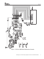
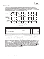
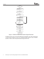
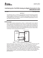
Application Brief SLAA070 - April 2000 Interfacing the TLC5510 Analog-to-Digital Converter to the TMS320C203 DSP Perry Miller Mixed Signal Products ABSTRACT This application report is a summary of the application note titled Interfacing the TLC5510 Analog to Digital Converter to the TMS320C203 DSP (literature number SLAA029) that presents guidelines for interfacing the TI TLC5510 analog-to-digital converter (ADC) to the TI TMS320C203 DSP. The TLC5510 is a CMOS, 8-bit, 20 MSPS (megasamples per second) ADC utilizing a semi-flash architecture. EVM Overview The TLC5510 includes internal-reference resistors, a sample-and-hold circuit, and 8-bit parallel outputs with high-impedance mode. The use of an evaluation module (EVM) is recommended due to the sampling rate of the TLC5510. Typically, when the sampling rate of an ADC exceeds 1 or 2 MHz the board layout is critical to the performance of the ADC, and the use of a breadboard for evaluation is no longer suitable. Figure 1 shows a simple example of how the TLC5510 EVM interfaces with the TMS320C203 development module (DVM). Control-logic circuits are used to access the data bus. TLC5510 EVM TM S320C203 DVM [D1:D8] [D0:D7] CLOCK IN CLKOUTI 15 A11 OE IS GND GND Figure 1. TLC5510 to TMS320C203 Block Diagram Figure 2 illustrates the various jumper locations on the EVM board. The EVM must be provided with three (3) separate voltages: analog (5 V: J2, –5 V: J3), and digital (5 V: J8). The –5 V supplied to the EVM is used as the negative supply voltage to the operational amplifier. Depending on the operational amplifier used to drive the ADC, this negative voltage may not be required in the actual application. The digital ground area for the digital-supply voltage is isolated from analog ground to prevent noise spikes, generated by the digital logic, from affecting the analog circuits on the board. The two grounding areas can simply be connected together with a jumper from E21 to E22, or from E13 to E14. This helps to create and evaluate alternate grounding options. 1 SLAA070 The analog-input signal is brought into the EVM through BNC connector J4. The reference voltage for the TLC5510 is generated by internal resistors. The analog input range of the TLC5510 is determined by the configuration of jumper J6 (inserted: 0 V–2.28 V; not inserted: 0.6 V–2.6 V). See the Texas Instruments data sheet for the TLC5510 and TLC5510A 8-bit high-speed analog-to-digital converters for information regarding other voltage settings. The user may select from four techniques to interface this analog input signal to the TLC5510: 1. Direct: the input signal can be directly fed to the ANALOG IN pin of the TLC5510 device. 2. Via the amplifier input using dc coupling 3. Via the amplifier input using ac coupling 4. User-defined input: an optional circuit extension allows additional tests to be performed. Refer to the application note titled Interfacing the TLC5510 Analog to Digital Converter to the TMS320C203 DSP, literature number SLAA029 (available at www.ti.com/sc/docs/psheets/ abstract/apps/slaa029.htm) for a detailed description of these four (4) types of interface techniques. The maximum conversion rate of the TLC5510 ADC is 20 MHz. The 20-MHz clock signal is fed via the BNC input J1. Two 74AC11004 inverters buffer this signal before it is applied to both the clock pin of the TLC5510 and to J5–22. 2 Interfacing the TLC5510 Analog-to-Digital Converter to the TMS320C203 DSP SLAA070 – Figure 2. TLC5510 to TMS320C203 DVM Interface Schematic Interfacing the TLC5510 Analog-to-Digital Converter to the TMS320C203 DSP 3 SLAA070 Data Transfer The TLC5510 analog-input data is sampled at the falling edge of the clock signal. The conversion time of the analog-input signal amounts to 2.5 clock cycles. Figure 3 shows the timing behavior of the TLC5510. The digital data is valid after a delay time tdd of 30 ns. Several important parameters of the TLC5510 are summarized in Table 1. tw(H) tw(L) CLK (Clock) ANALOG IN (Input Signal) N+1 N+2 N D1–D8 (Output Data) N+4 N+3 N–3 N–2 N–1 N N+1 tpd Figure 3. TLC5510 I/O Timing Diagram Table 1. TLC5510 Parameters PARAMETER TEST CONDITIONS Pulse duration, clock high, tW(H) Maximum conversion rate BW Analog input bandwidth tdd Delay time, digital output NOM MAX 25 Pulse duration, clock low, tW(L) fconv MIN VI(ANLG) = 0.5 V – 2.5 V At –1 dB UNIT ns 25 ns 20 MSPS 14 At –3 dB 23 CL ≤ 10 pF 18 MHz 30 ns A schematic of the TLC5510 EVM interface to the TMS320C203 DVM is shown in Figure 2. The TMS320C203 DVM is a standalone board carrying a TMS320C203PZ DSP, an analog-interface circuit (AIC), flash memory, SRAM, and serial interface for communication with a PC via the serial COM port. The fixed point TMS320C203PZ has an instruction cycle time of 50 ns and is optimized for efficient implementation of digital-signal-processing algorithms. Referring to Figure 2, the data bus (D1 – D8) is connected via data-bus driver SN74AC573 (J5 pins 2, 4, 6, 8, 10, 12, 14, and 16) through a short ribbon cable to the TMS320C203 DSP databus lines (D0 – D7). To prevent bus contention, the SN74AC573 device must be in an active state only when data is being read from the ADC. Each time the DSP wishes to read data from the ADC, address line A11 is set to a logic-high level, and IS is set to logic low. A11 and IS form the inputs to the control logic that drives the OE pin to logic low and thus switches data bus driver SN74AC573 from 3-state to an active state. 4 Interfacing the TLC5510 Analog-to-Digital Converter to the TMS320C203 DSP SLAA070 Software Overview The program editing and assembly are performed on the host PC and downloaded to the TMS320C203 DVM for real-time processing. The DSP executes the interface program and acquires and processes n input samples from the ADC. Figure 4 shows the program flow chart. The program starts with a common initialization procedure for the DSP, followed by initialization of several auxiliary registers (ARs). The following steps define the program constants: 1. Set data page pointer to 0h 2. Set starting address 3. Set number of samples 4. Set A/D address The program executes the following steps: 1. On interrupt, disable global interrupts and save PC, ARs, and status registers. 2. Initialize the C203 DSP. 3. Load the appropriate ARs. 4. Send the device address to the TLC5510, loading the A/D output into memory. 5. After obtaining a predefined number of A/D converter samples, the DSP exits the loop subroutine. 6. Restore the PC, status registers, and ARs. 7. Enable global interrupts. The data is now available for use in customer-defined functions (algorithms). Interfacing the TLC5510 Analog-to-Digital Converter to the TMS320C203 DSP 5 SLAA070 START SET dma POINTER SET A/D ADDR SET SAMPLE COUNTER = n CONTEXT SAVE RET ADDR, AR1, AR0, ST1, AND ST0 INITIALIZE DSP LOAD NEW VALUES IN ARs AND ARP GENERATE A/D ADDR PROCESS RECEIVED DATA NO # OF A/D SAMPLES READ = n? YES CONTEXT RESTORE ST1, ST0, AR1, AR0, AND RET ADDR ENABLE INTERRUPTS FUNCTION END Figure 4. TLC5510 to TMS320C203 Interface Program Flow Chart C-callable assembly code can be downloaded from the application note titled Interfacing the TLC5510 Analog to Digital Converter to the TMS320C203 DSP, literature number SLAA029, available at www.ti.com/sc/docs/psheets/abstract/apps/slaa029.htm 6 Interfacing the TLC5510 Analog-to-Digital Converter to the TMS320C203 DSP SLAA070 Summary This application brief shows the hardware and assembly-code implementation required to interface the TLC5510 analog-to-digital converter (ADC) to the TMS320C203 DSP. Many other analog components play a part in the entire system. Operational amplifiers are needed for signal conditioning, and voltage regulators are required to supply various voltages on the board. The following are additional parts from Texas Instruments to be considered when designing the system described in this application brief: • • • • • • • • THS3001 – High speed operational amplifier, 420 Mhz GBW THS4001 – High speed operational amplifier, 300 Mhz GBW TPS7150 – Low dropout regulator, 5 V/500 mA TPS7250 – Low dropout regulator, 5 V/250 mA TPS7350 – Low dropout regulator, 5 V/250 mA / supply voltage supervisor TLC7705 – Supply voltage supervisor TPS3823-50 – Supply voltage supervisor TPS3823-50 – Supply voltage supervisor For more detailed information refer to the following literature numbers and titles: LITERATURE NUMBER DOCUMENT/TITLE SLAA029 Application report : Interfacing the TLC5510 ADC to TMS320C203 DSP SLAS095I Data sheet: TLC5510, TLC5510A 8-Bit High-Speed Analog-to-Digital Converters SLAD001 Data book: Data Acquisition Circuits, Data Conversion, and DSP Analog Conversion Interface SLAU007 TLC5540/TLC5510 Evaluation Module SPRU127B User’s guide: TMS320C2xx SPRU018D User’s guide: TMS320C1x/C2x/C2xx/C5x Assembly Language Tools SLOS217 Data sheet: THS3001 SLOS206 Data sheet: THS4001 SLVS092C Data sheet: TPS7150 SLVS102C Data sheet: TPS7250 SLVS124A Data sheet: TPS7350 SLVS087I Data sheet: TLC7705 SLVS165A Data sheet: TPS3823–50 SLVS165A Data sheet: TPS3824–50 SCAS033B Data sheet: 74AC11004 Hex Converter SPRS025 Data sheet: TMS320C203, TMS320C209,TMS320LC203 Digital Signal Processors SCLS319E Data sheet: 74AHCT1G04 Single-Inverter Gate SCLS317G Data sheet: 74AHC1G32 Single 2-Input Positive-OR Gate World Wide Web Our World Wide Web site at www.ti.com contains the most up to date product information, revisions, and additions. A TI C2xx Development System User’s Manual is also available from Wyle Electronics at www.wyle.com. Interfacing the TLC5510 Analog-to-Digital Converter to the TMS320C203 DSP 7 IMPORTANT NOTICE Texas Instruments and its subsidiaries (TI) reserve the right to make changes to their products or to discontinue any product or service without notice, and advise customers to obtain the latest version of relevant information to verify, before placing orders, that information being relied on is current and complete. All products are sold subject to the terms and conditions of sale supplied at the time of order acknowledgment, including those pertaining to warranty, patent infringement, and limitation of liability. TI warrants performance of its semiconductor products to the specifications applicable at the time of sale in accordance with TI’s standard warranty. Testing and other quality control techniques are utilized to the extent TI deems necessary to support this warranty. Specific testing of all parameters of each device is not necessarily performed, except those mandated by government requirements. Customers are responsible for their applications using TI components. In order to minimize risks associated with the customer’s applications, adequate design and operating safeguards must be provided by the customer to minimize inherent or procedural hazards. TI assumes no liability for applications assistance or customer product design. TI does not warrant or represent that any license, either express or implied, is granted under any patent right, copyright, mask work right, or other intellectual property right of TI covering or relating to any combination, machine, or process in which such semiconductor products or services might be or are used. TI’s publication of information regarding any third party’s products or services does not constitute TI’s approval, warranty or endorsement thereof. Copyright 2000, Texas Instruments Incorporated