1
AD1100User'sManual
ffi
Inc.
RearTimeDevices,
" Accessing
theAnalogWorld'*
ISO9001 and AS9100 Certified
User'sManual
ffi
INC.
REALTIMEDEVICES,
Drive
820 NorthUniversity
PostCIficeBox906
16804
StateCollege,Pennsylvania
Phone:(814)234-8087
FAX:(81a)234-5218
Publishedby
RealTime Devices,Inc.
820N. UniversityDr.
P.O.Box 906
StateCollege,PA 16804
CopyrightO 1991by RealTime Devices,Inc.
All rights reserved
Printedin U.S.A.
Rev.C 9243
TABLE OF CONTENTS
Page
INTRODUCTION
How to Use This Manual.......
When You Need HelP.
CHAPTER I - QUICK START-GETTING
What ComesWith Your AD1100...........,..
The Hardware..............
You CanSet.............
Functions
Setting the Base I/O Address
InstallingttreADllOOin YourComputer....
""""""""'i-2
""""J-2
YOUR AD1100 RUNNING
TheSofuvare
DemoDisk
BackingUpYourDisk...........
InitializingYour AD1100
Selectingan Analog Input Channe1................
Settingthe Input Gain...........
Takingan A/D Reading......
CHAPTER 2 - FUNCTIONAL DESCRIPTION
Analog-to-DigitalConversionCircuiry...............
Multiplexer..
GainControlCircuitry.....
SampleandHold Circuitry...'.
AID Converter
lnterface...'..
ProgrammablePeripheral
IntervalTimer(PIT)
Programmable
CHAPTER 3 - JUMPER SETTINGS
m,n,and P4- InterruptHeaderConnectors..
P2 - AID End-of-Convert(EOC) Interrupt......
P3 - PIT Output Interrupts....
P4- EXTINT andPPIINTRA Intemrpts....
IntervalTimer (PIT) I/O HeaderConnector....
Programmable
P5
HeaderConnector....
P6- BaseVO Address
(EOC)
MonitorHeaderConnector...
P8 End-of-Convert
VoltageRangeHeaderConnector....
P9- A/D Converter
Gain...........
Configurable
Resistor
JumperJl-Externall/OConnectorP7,Pin40Configuration..............'
""""""""' l-l
""""" 1'1
""""" 1-1
""""""'L-2
14
"""""""""'
"""'14
16
""""""""""'
""""""' 16
"""" 1-6
""""""' l-7
"""""""" 1-7
""'l-7
""""2-I
"""""""""'2-l
"""""""""'2'I
"""""""2-2
""""""""'2'2
""""'2'2
""""""'2-3
"""""""3-2
""3-2
""""'3-2
"""""" 3-3
3-3
"""""""""""'
3-5
"""""""""'
.....""""""' 3-6
......""""""' 3{
""""""' 36
"""""""3'7
Page
CHAPTER 4 - PROGRAMMING YOUR ADl1OO
Selectingan Analog Input Channe1................
Settingthe Input Gain...........
TakinganA'/DReading.............
PeripheralInterface......
Programmingthe Programmable
IntervalTimer.........
Programming
theProgrammable
Ilardware
Intemrpts
(EOC)Signal.........
End-of-Convert
4/p
PPIIntemrpt
PITIntemrpts
ExternalIntemrpt
CHAPTER 5 - CALIBRATION PROCEDURES
RequiredEquipment.............
A/D Calibration
APPENDIX A - AD1100 Specifications
APPENDIX B - Connector Pin Assignments.......'.........
APPENDIX C - ComponentData Sheets........
APPENDIX D - Configuring the ADllOO for SIGNAL*MATH
APPENDIX E - Configuring the AD1100 for ATLANTIS....'..
APPENDIX F -Warranty...........
.............4-1
..........-..-..4-l
............."'4-1
...........-----.4-1
-..-..4-l
.................4'2
4-3
.................
.................-.4-3
.............-----4-3
........""'4-3
5-1
.....................
..............--.-...5-2
..........'A-1
.....B-l
....'..........'....C-1
..........D-1
............E-l
......F-1
LIST OF ILLUSTRATIONS
Figure
i-1
1-1
1-2
1-3
r4
2-l
2-2
3-l
3-2
3-3
34
3-5
34
3-7
3-8
3-9
4-l
5-1
Page
Typical Laboratory Setup..........
AD1100 Board Layout........
BaseVOAddressHeaderConnects,P6............
PPIModeDefinitionFormat........
A/DConversionWordFormat
ADl100 FunctionalBlock Diagram
EOC Timing Diagram.
AD1l00 Board Layout........
IntemrptHeaderConnectorP2
IntemptHeaderConnectorP3
IntemrptHeaderConnectorP4
PIT VO HeaderConnectorP5
PIT FunctionalBlock Diagram
P8..............
Connector
EOCMonior Header
Header
ConnectorP9
Range
Voltage
AID Converter
Gain ConfigurationSchematicDiagram......
PPIModeDefinitionFormat........
AD1f00 Board Layout........
t,
"""i-1
"""""'l-2
""' 14
""'l-7
"""""' 1-8
""2-l
"""""""""2-2
"""""'3-1
"""""'3'2
"""""'3'2
"""""' 3-3
""""""34
"""".' 3-5
."""' 36
......."""""' 3{
""""'3-7
""'4'2
"""""'5-1
LIST OF TABLES
andSettings
AD1l00 BoardFunctions
AD1100VO Map......
Bit Weights
A/D Converter
Page
1-3
..................
..'. 1-5
....--.-.-.....5-2
INTRODUCTION
forRealTimeDevices'ADl l00generalpurposedata
technicaldata
Thismanualshowsyouhowto operateandprovides
conversion.
12-bithigh-speedanalog-to-digital
single-ended
acquisitionboard.The ADl100 featureseight-channel,
real-time
in
the
operate
to
effectively
computer
your
or
compatible
PCDru/AT
IBM
allows
interface
This versatile
1
a typical
Figure
ishows
digital
signals.
generate
and
analog
sense
and
to
and
control
environmentof dataacquisition
PC
for
data
collection.
laboratorysetupusing a
llf0sKsrnrl 0H
[RBORnTURT
HRRtrII|BRE
tEMPCor
Compotlble
SOTTUNRE
datareduction'
D ocqulsltion,
Signalcondltionlng
control,dotastorEgB
graphlcs,
analgsls,
NUTOHRTION
T R BOERTORY
Fig. i-1 - TyPicalLaboratorySetuP
thatprovide
(12-bit)analog-to-digital
converter,digitalI/O, andtimer/counters
TheADl l00 featuresahigh-resolution
planes,
ground
flexibility for many applications.Its double-sidedconsfiuctionprovides separateanalogand digital
(short
or
enhancingboardperformanceand low-noisecharacteristics.It plugsdirectly into any unusedexpansionslot
attherearpanel
areaccessible
includingPCbus-sourcedpower,
AllexternalVOconnections,
fug-size)in thecomputer.
of thecomputerwhentheboardis installed.
Throughprogrammingand/
Severalof theAD1100'sfunctionscanbe readilyadaptedfor your specificrequirements.
or jumpersettingsmadeon theboard,you can:
. SelectthebaseI/O address,
. Selectthe activechannel,
. Setthe gain,
. Selectthe analoginput voltagerange,
. Controlz4T'ILICMOS-compatibledigitalI/O lines,
. Control three l6-bit, 8 MHz timer&ountercircuits (theprogrammableinterval timer),
. Monitor theA/D conversionusingthe end-of-convert
(EOC)signal,
. GenerateintemrPtsignals.
Many of these functions are set up at tlle factory, based on typical data collection requirementsand customer
installandrun theADl100 with minimalunderstanding
whenordering.Therefore,youcansuccessfully
specifications
everythingaboutyourboardso
aboutchangingandconEollingthem.On theotherhand,you may wantto understand
thatyou caneffectivelyuseeachfeature.With thisin mind,thismanualprovidesbasicinformationo gettheboardup
of eachfunction.
andrunning,aswell asdetailedinformationfor a full understanding
i-1
How to UseThis Manual
This manualis designedto helpyouinstallandgetyourADl 100runningquickly,while alsoincludingsufficientdetail
abouteachboardfunction. Begin by readingChapterI in order to useyour boardas quickly aspossible.This chapter
yourADl l00packagewillallowyouto Fomptlyuseyour
softwareincludedwittr
andtheaccompanyingdemonstration
readChapters2 through4. Chapter5 containsboard
AD1100
functions,
ttre
control
and
To
fully
understand
interface.
procedures.
calibration
The chaptersand appendixesin this manualaredescribedin detail below.
to
Chapter1, "Quick Start---GesingYour ADl100 Running,"providesthe insructionsnecessary
not
cover
does
this
chapter
in
insall theboardanduseits basicfunctions.The informationcontained
how to changethe boardseftp, exceptfor thebaseI/O address.
Chapter2, "Functional Description,"providesa block diagfamand a functional discussionof the
board.
'TumperSetdngs,"describeseachheaderor jumper circuit on the boardand how it is
Chapter3,
controlled.
Chapter4, "ProgrammingYour ADI100," describeshow the boardcanbe programmedusingthe
demonstrationsoftware.
Chapter5, "CalibrationProcedures,"providesinstructionsfor boardcalibration.
*ADl100 Specifications,"
concains
a completelisting of boardspecifications.
AppendixA,
thepinoutof theextemalI/Oconnectorandthe
AppendixB,"ConnectorPinAssignments,"conlains
number.
matingconnector'sPart
Appendix C, "Component Data Sheets,"contains manufacnren' data sheetsfor major board
components.
AppendixD,'Configuring theADll00 for SIGNAL*MATH," containsinformationabut setting
boardjumpen and and initializing the boardto run the SIGNAL*MATH acquisitionand analysis
progam.
AppendixE, "ConfiguringtheADI100 for ATLANTIS," conlainsinformationaboutsettingboard
jumpersto run the ATLANTIS dataacquisitionandreal-timemonitoringprogam.
AppendixF, "Warranty," containsboardwarrantyinformation.
When You NeedHelp
Whenyou areworking with the ADI100 interfaceboard,this manualandthedemosoftwareincludedin your package
toproperlycontrolallof theboard'sfunctions.If,however,aftercarefullyreviewing
will providesufficientinformation
from theboard,RealTime Devices'technicalstaff is readyto assist
themanual,youareunableto obtainproperresponses
(Sla)
regular
businesshours,easternstandardtime or easterndaylight time,
during
234-8087
you. For assistance,call
(814)
2y-5218.
Be sureto includeyour company'sname,your name,your
to
or senda FAX requestingassistance
problem.
the
of
telephonenumber,anda brief description
i-2
CHAPTER 1
QUrCK START4ETTING YOURAD1100RUNNING
To get stafledusingyour ADl100 interfaceboard,you must:
- Selectby jumpera baseI/O addresswhichdoesnot contendwith any otherperipheraldevice.
- Install the boardinto your PC.
- Connecta signalto oneof theanaloginputchannels.
- Run theADl100 software.
thesestepsareall thatarenecessary
to useyour ADl100 board.
Unlessyou haveotherrequirements,
This chapterexplainshow to installyour ADl100 anduseits basicfunctions.You will learnhow to:
. Changethe baseI/O addresssetting,
. Install the boardin your PC,
. Initializetheboard,
. Selectthe analoginput channel,
. Take an A/D reading.
This chapterallows you to immediatelystartusing the basicfunctionsof your AD1100 boardfor datacollection
applications.This chapterdoesnot explain how to control the more intricate board functions such as the resistorconfigurablegain, the programmableinterval timer, the variousdigital I/O configurations,or intemrpts,nor doesit
settingsexceptfor thebaseI/O address.The functionsnot coveredhereare
explainhow to changehardware-controlled
describedin Chapters2 through4.
What ComesWith Your AD1100
The standardADl100 boardpackageincludes:
I
I
I
ADl100 5.4-inch(l37mm)interface
board
AD1100demodisk
user'smanual
applicationsoftware,areavailableforthis
Additionalitems,suchasextenderboardsorSIGNAL*MATHoTATLANTIS
boardand are includedon an asorderedbasis.
with RealTime Devices'XB40 VO extenderboardand XC40
All signalson your boardare madeeasilyaccessible
expansioncable.The extenderboardhastwo 20-pinterminalsfips anda protorypeareato supportany specialcircuitry
relaysor optoisolators,
youmayrequireto condilionthesignals.For example,if youareproiotypingsolid-state
thiscan
easily be done with an XB40. The expansioncable terminatesin a 40-pin wire-wrap headerconnectorsuitablefor
installationin standard0.1 inch spacingperf-boardmaterialavailablefrom mostelectronicdistributors.
The Hardware
The ADI100 interfaceboardis shownin Figure 1-1.A completelisting of the boardspecificationsis containedin
Appendix A. The ADl100 hasseveralfeatureswhich are user-conrolledthroughhardwareor software.Most of the
gain is component-controlled.
featuresarejumper-controlled
andtheresistor-configurable
hardware-controllable
aremountedon a 5.4-inchprintedcircuitboardwhichfits in anyunusedshortor full-size
All of theboardcomponents
P7,accommodates
all of theboard's
expansionslotin anIBM PC/XT/ATor compatiblecomputer.A 40-pinconnector,
externalVO.
FunctionsYou Can Set
To allow theADl100 interfaceboardo be adaptedto your needs,severalfunctionscanbe setup to performspecific
tasksby changingthe hardwareconfigwationor throughsoftware.Table l-1 lists eachfunctionyou cancontrol,the
facory (or default)settingif applicable,andwherein thismanualyou canfind informationaboutis settings.
1-l
J0
;r5
!*
,,, AD1100
Br
12.BIT HIGH€PEED
ANALOG Ilo BOARD
E6i
rc
"'n
U-t
"'n
"'n
U5-rU-l
Fig. 1-1 - AD1100BoardLayout
The functionswhich you cancontrol throughhardwareare:
- BaseI/O address,
- Analoginputchannelvoltagerangeandpolarity,
- Analog input gain (resistor-configurable)
- End-of-convertmoni[or,
- PIT timer/counters(hardwareand software),
- Interrupts.
The functionswhich you cancontrol throughsoftwareare:
- Analoginputchannelselection,
- Digital I/O,
- PIT timer/counters(softwareand hardware),
- Boardinitialization.
Settingthe BaseVO Address
in yourcomputer'sI/Ospace.
Startingwittrthebasel/Oaddress
@A), theADl l00uses20consecutiveaddresslocations
I/O address
locations
Table1-2liststtrel/Omapfor theADl100.Itis importanttorecognize
thatsomeofyourcomputer's
If yourADl100 boardtriesto useI/O addresslocations
will alreadybe occupiedby internalI/O andotherperipherals.
alreadyin useby anotherdevicein your system,addresscontentionwill result.Hence,theboardwill not operate,or at
bestwill operateerratically.
when addingan interfacedeviceto yoru
I/O addresscontentionis one of the most commonproblemsencountered
jumpercircuitisprovidedon
By changing
theAD1100board.
computersystem.Toavoidthisproblem,abaseVOaddress
thepositionof thejumperon theheaderconnectorlabeledP6 (locatedjust to theleft of center,nearthebottomof ttre
board),thebaseI/O addresssettingcanbe changedto anyoneof eightlocations.
1-2
T a b l e 1 - 1 - A D l 1 0 0 B o a r d F u n c t i o n sa n d S e t t i n g s
FUNCTION
FACTORY SETTING
USER INFORMATION
Basel/OAddress
300hex(768decimal)
To changethissetting,see
"Settingthe Basel/O
Address,"
Chapter1
AnalogInputChannel
Selection
lable
Software-control
an Analog
See"Selecting
lnputChannel,"
Chapter1,
anddemodisk
AnalogInpulGain
nfigurable;
Resistor-Co
factory-setto 1
igurable
See "Resistor-Conf
Gain,"Chapter3, anddemo
disk
AnaloglnputVoltageRange
whenordering To changethissetting,seeP9
User-specified
Chapter3.
discussion,
(EOC)Monitor Connected
to PB7
End-of-Convert
See PBdiscussion,
Chapter3.
Digitall/O
lable
Software-control
the PPl,"
See"Programming
Chapter4 anddemodisk
Modes
lable
Software-control
the PlT,"
See"Programming
Chapter4 anddemodisk
l/O Configuration
ClockInput:5MHz
Gatelnput:+5 V
ClockOutput:To P7
Chapter3
See P5 discussion,
Disabled
See P2,P3,and P4
discussions,
Chapter3, and
"lnterruptConsiderations,"
Chapter4
24llo LineslromPPI
Timer
Programmable
Interval
(PlT)Circuitry
Interrupts
External Connected
to GND
JumperJl (Controls
l/OConnector
P7,Pin40)
SeeJumperJ1 discussion,
Chapter3
headerconnector,
P6,with thejumperinstalledat ttrefactory-setlocationof 300
FigureI -2 showsthebaseI/O address
of pinsonP6.ThehexadecimalbaseVOaddress
acrossoneof
theeightpairs
hex.Thejumpermustbeinstalledvertically
pins,
from left to right, is asfollows:
to eachpair of
settingcorresponding
200
240
280
zCA
300
340
380
3C0
listedin Table1-2,BA equals280.
is changedo 280hex,thenfor the20 operations
For example,if thebaseI/O address
Thus,to selectanaloginput channel8, its addressof BA + 7 becomes287hex.
If thefactorysettingof 300hexwill causecontentionin yoursystem,positionthejumperto thedesiredbaseVO address
makea noteof its valueonthetableinsidethebackcoverof thismanual.
setting.OnceyouhavesetthebaseI/O address,
You will needto know this seuingfor usein your programs.
Ess TE
NCD(!)
c) cr)
P6
Fig.1-2-
Base l/O AddressConnector,P6
Installingthe AD1100in Your Computer
BeforeinstallingtheADll00 in yourcomputer,makesurethatthebaseI/O addresshasbeenproperlyselectedandall
thehardwaresettingshavebeenconfiguredto supportyour requirements.This chapterexplainshow to control thebase
aslistedin Tablel-1, andremainat theirfactorysettingsunless
I/O address.
Otherhardwaresettingsaresetatthefactory,
whenyou receiveyourboard.
by yourADl 100aredisabled(notconnected)
youchangethem.Theinterruptsgenerated
If you intendto usetle intemrpts,theymustbe configuredappropriatelybeforeinstalling theboard.Informationabout
2 tlrrough4. Usethesechaptersasnecessary
theseandotherfunctionsnotcoveredin thischapteris providedin Chapters
to configureyour boardbeforeinstallation.
To installyour ADll00, follow thesestepby-stepprocedures:
1.TURN OFFTI{E POWERTO YOUR COMPUTERFIRST.Refero theowner'smanualfor your
computer,andremovethe topcover.
2. Selectanunusedexpansionslot (shortor full-size)in whichto installyourboardandremoveits
blankbracketfrom therearpanelof thecomputerby removingthescrewat the
corresponding
top of the bracket.
throughtherearpanelopeningand
3. Orienttheboardinsidethecomputerso thatP7 is accessible
Then,pressdown
onthemetal
slotconnector.
upwith theexpansion
thecardedgeconnectorlines
slotconnector.
thetopoftheboarduntiltheboardis firmly seatedintheexpansion
brackettaband
4. Securethe bracketbackin placewith thescrewandput thecoverbackon your computer.
Now your boardis readyto be connectedvia the externalconnectorat the rearof the computer.After this connection
hasbeenmade,the boardis readyfor operation.
The Software
includesselectingtheanaloginputchannel,controlof the
undersoftwarecontrol.Programming
TheADl100 operates
peripheralinterface,andcontrolof theprogrammable
intervaltimer.
theA/D conversion,controlof theprogrammable
The analoginput channelselectionandtakingan A/D readingarecoveredin this chapter.Digital I/O conrol tlrough
in Chapter4,"Progmlxming
intervaltimeraremorecomplex,andaredgscribed
thePPIandcontrolof theprogrammable
"Jumper
gain
in
3,
Settings."
is
Chapter
described
Your ADl100." Theresistor-configuarable
I-4
Table 1 - 2 - A D 1 1 0 0 l / O M a p
FUNCTION
A4
A3
A2
A1
AO
R/W
BA + HEX
0
0
0
0
0
0
0
0
0
0
0
0
0
0
0
0
0
0
0
0
0
0
1
1
0
0
1
1
0
1
0
1
0
1
0
1
w
W
W
W
W
W
W
W
0
1
2
3
4
5
6
7
0
0
0
0
1
1
1
1
0
0
0
0
x
0
1
0
1
W
W
0
0
0
0
1
1
1
1
1
1
1
1
0
0
R/W
R/W
R/W
W
c
1
1
0
1
0
1
1
1
1
1
0
0
0
0
0
0
0
0
0
0
1
1
0
1
0
1
R/vV
R/W
R/W
W
10
11
'12
AnaloglnputChannel
AINl
AIN2
AIN3
AIN4
AIN5
AIN6
AINT
AINS
A/DConversion
Circuitry
Start12-bitConversion
Start8-bitConversion
ReadMSB
ReadLSB
1
1
1
1
X
x
x
R
R
8 orA
9orB
Bo r A
9orB
PPI
PortA
PortB
PortC
ControlWord
Timer
Interval
Programmable
Counter0
Counter1
Counter2
ControlWord
NOTE:x= don'tcaresetting
D
E
F
13
Regardlessof what programminglanguageyou use,you can write programsthat control ttre ADllOO board.The
your ADl100 containsexamplesin TurboC, TurboPascal,andBASIC.
disk which accompanies
demonstration
Nearly all modernMS-DOS-basedPC languageshaveVO referenceinstructions.Theseare ttreinstmctionsto control
thedataransfers to andfrom theVO ports.Consultyour programminglanguagereferenceto find theseinstructionsfor
your favorite language.Listed below arethe VO referenceinstructionsusedby somecommonlanguages.
inpun
outpur
BASIC
INP
ouT
TURBO PASCAL
Port
Port
TURBO C
inportb
outportb
DemoDisk
Includedwittr your ADl100 is a demodisk which providesprogramminginstructionsand exampleprogramsfor
controllingthe functionsof your interfaceboard.This demodisk is dividedinto directories,eachof which is named
accordingto the languageusedto write the programsit contains.The files wittrin each directory con[ain example
programsanda documentation
file with generalinformation.In addition,your demodisk containsa README.DOC
programming
provides
information for your board.
file which
Each exampleprcgam showsyou how to control a particular board function, such as selectingan input channel,
controllingtheA/D converter,controllingdigital datafansfers,andsettingthetimer/countercircuitry. Theseprograms
shouldbe usedto becomefamiliarwith thesefunctions.
BackingUp Your Disk
formatwhichcanbereadbyall DOSversions1.1andabove.
Thedemodiskprovidedwith theADl100 is a double-sided
Beforeusingthesoftwareincludedwith yourboard,makea backupcopyof thedisk.You maymakeasmanybackups
disk, insertthedisk to be copiedinto drive A of your
as you need.To copy ttreoriginalto any otherDOS-formatted
computer,and from DOS enter:
COPY A:*.* B: (or otherdestinationdrive specifier)
Initializing Your AD1100
Beforeyou canoperatethe ADll00, you may haveto initializeil. Initializationis requiredto configurethePPI.For
signalthroughbit 7 of oneof its threeports.To
example,it mustbe configuredwhenyou monitorthe end-of-convert
initialize thePPI for your application,this stepmustbe executedeverytime you startup,reset,or reboottle computer.
locationsin thecomputer'sVO space.Tablel-2providestheADl100
As described
earlier,theADI100 uses20 address
controls.Recallthat thebaseI/O addressis factory-setat 300
I/O map,defining whatfunction eachof the20 addresses
hex.On thedemodisk, thebaseI/O addressis usuallystoredin tlte variable"board." Remember!o usethecorrectbase
I/O addressin thedemodiskprognmsor yourownprcgrams.Thedemodisk explainshowto changethebaseI/O address
in theprograms.
The ADl l00 is initializedby simplywriting a controlbyteto thePPIcontrolregistermappedat the VO locationbase
2and4 andthedatasheetinAppendix
address+F (hex).Figure1-3showsthestructureof thePPIcontrolword.Chapters
C explain the meaningof eachbit settingin the control word.
For example,recallthattheEOC signalis factory-setto be monitoredthroughport B, bit 7 (PB7).To properlysetup
the PPI so port B is an input port, t}le connol byte mustconformto this generalform:
lxxx x01x (decimal130)
wherex=don'tcale
This configuresport B asa mode0 input"which is requiredif you aremonitoringtheEOC throughPB7.
l-6
D7
D6 D5 D4
D3 02 D 1 DO
I
GROUPB
PORTC (LOWER)
1 = INPUT
O= OUTPUT
PORTB
1 = INPUT
O= OUTPUT
MODESELECTION
0 = ITTODE
0
1 = [40DE 1
GROUPA
PORTC (UPPER)
1 = INPUT
O= OUTPUT
PORTA
1 = INPUT
O= OUTPUT
MODESELECTION
00 = MoDE0
01 = MODE1
1X= MODE2
MODESET FI-AG
1 = ACTIVE
Fig. 1-3 -
PPI Mode DefinitionFormat
Selectingan AnalogInput Channel
After the ADl100 hasbeeninitialized you canselecttheanaloginput channel.The analoginput channelis selectedby
writingtooneoftheeightl/OlocationsBA+0throughBA+?.Tablel-2showstheVOlocationsandtheirconesponding
channels.The datawritten is irrelevanl The act of writing activatesthe selectedchannel.After a [nwer reset,all eight
channelsare disconnected.
Settingthe Input Gain
TheADll00 featuresa uniquegainconfigurationcapability.Byremovingaboardjumperandinstallingsomeresistors,
the gaincanbe changedfrom the facory settingof 1 (unity) to whateveryou desire(greaterthan l). In this chapter,the
facnry settingof 1 is used;later chaptersdetail this feature.Chapter3 showshow to set up the resistorgain.
Taking an A/D Reading
After youhaveselectedananaloginputchannel,youcantakeanA/D reading.It is importantto notethatoncethechannel
is set,it staysat that settinguntil you changeiq that is, it is latchedaslong asyour systemis poweredup. You do not
have!o set the channelevery time you take a reading.
Each time an A/D conversionis completed,an end-ofconvert (EOC) signal is generatedto signify the end of the
conversion.This signalcanbeusedin a numberof ways.Oneway is to usethisline to monitortheA/D conversionstatus.
configuringbitTofPPIportA,portB,orportCasaninputlineand
SeuinguptheEOCsignaltobemonitoredinvolves
connectingtheEOC signalo it. This procedureis detailedin Chapter3, "JumperSettings."TheEOC signalis factoryset to be monitoredthroughPB7 on headerconnectorP8.
t-7
The generalalgorithm for taking an A/D readingis:
+ 8 (or A):
1. Starta 12-bit conversionby writing to base-address
out base-address+8,0
(Note that the valueyou sendis not important.The act of writing o this VO location is the key
to startinga conversion.)
or monitorPPI port A, B, or C, bit 7 for a transition.Polling
2.Delay at least20 microseconds
permitsthe fastestdataacquisition.
+ 9 (or B):
3. Readtheleastsignificantbit from base-address
+9)
lsb%o= inp(base-addressTo
+ 8 (or A):
4. Readthe most significantbit from base-address
+8)
msbTo= inp(base-addressTo
5. Combinetheminto rhe 12-bitresultby shiftingtheLSB four bits o therighr The MSB must
also be weightedconectly:
resultTo= (msb7o* 16) + 0sb%oll6)
For a 12-bitconversion,the A/D datareadis left justified in a l6bit word, with the leastsignificant fourbits equalto
of *ris,thetwobytesof A/D datareadmustbescaledto obtaina validATDreading.
zero,asshowninFigure14. Because
be
correlatedtoavoltagevaluebyscalingitandthenmultiplyingbytheappropriate
thereadingcan
Onceitiscalculated,
in
table
below:
the
bit weight,as shown
Input Range
+5 volts
t10 volts
ScaleFactor
Subract2048
Subract2048
Bit Weight
2.4414mY
4.8828mV
MSB
D 1 5 D 1 4 D 1 3 D 1 2 D 1 1 D 1 0 D9 D8 D7 D6 D5 D4 D3
DB12DB11D B l C D89 D88 D87 DB6 D85 DM D83 DB2 DB1 0
Fig.1-4 -A/D
D2
D1
LSB
DO
0
0
0
ConversionWord Format
For example,if theA/D readingis 1024andtheinput rangeusedis +5 vols, the analoginput voltage
is calculatedasfollows:
(luV+ - 2018)birs* 2.4r'.14mV/bit= -2.499p9vol16'
For a +10 volt input range,thevohageis calculatedasfollows:
(r0A - 2048)birs* 4.8828mV/bit= 4.99999 vols.
The bipolar input voltagerangeis factory-setaccordingto customerspecilicationswhen orderingthe board.If, after
receivingyour board,you wish to changethe input voltage,seeChapter3, "JumperSettings."
Note that eight-bit A/D conversionscanalsobe performed.This is accomplishedby writing to VO location BA + 9 (or
it is performedmuchmorerapidly,
B). While aneight-bitconversionhasa lowerresolutionthanthe l2-bit conversion,
youcan
Therefore,
whenspeedisessential,
A
takesabout20
microseconds.
l2-bitconversion
13
microseconds.
in about
capability.
usethe eight-bit conversion
l-8
CHAPTER2
FUNCTIONAL DESCRIPTION
showsablockdiagramof theboard.
themajorfunctionsof theADl l00interfaceboard.Figure2-1
Thischapterdescribes
The functionsdiscussedin the following sectionsare:
. Analog-to-digitalconversioncircuitry
. Programmableperipheralinterface@PI)
. hogrammable interval timer @IT) circuitry
Analog-to-DigitalConversionCircuitry
The main function of the ADl100 interfaceboardis to provide high-speedanalog+edigital conversioncapbility for
data acquisition.The analog-to{igital (A/D) conversioncircuitry receivesinputs from eight single-endedanalog
channels,selectsone active channel,and performsan analog-to-digttalconversionof the voltagevalue read at that
channel.The conversionthroughputrate is typically 38 kIIz.
Multiplexer
An eight-bit analogmultiplexeris used!o connectoneof eight single-endedanalogchannelsto the convertercircuiry.
A channelis selectedthroughsoftwarecontrol,by writing !o the appropriateVO location,asdescribedin Chapter1.
Gain Control Circuitry
The resistor-configurablegain connol circuitry canprovide a gain factor of 1 or greater.Theboardis facory-set for a
gain of 1 (no resiitors are installed;a jumper bypassesthe circuit). To changethis setting, seeChapter3, "Jumper
Settings."
BlockDiagram
Fig.2-1- AD1100Functional
2-l
Sampleand Hold Circuitry
A sampleand hold (S/tI) amplifier is usedbetweenthe gain control circuitry output and the A7D input to ensurethat
dynamicanalogsignalsareaccuratelydigitizedby ttreAID converter.The .001pF hold capacitorusedin this circuit is
time(6microseconds,
absorption.Itslowvalueminimizestheacquisition
apolystyrenetypeselectedforitslowdielecfic
theEOCsigral
typical),andminimizesholdstepvoltageanddroop.Thesampleandholdtimeandratearedeterminedby
generatedby the AID converterandfed backino the SAI circuir When ttreEOC signalis high (logic 1), the amplifier
samplesttreanaloginpuq when theEOC signalis low (logic 0), the amplifier holdsthe inpur
A./DConverter
TheA/D converteris a high-speedl2-bit conversionIC whichperformsconversionsin approximately20 microseconds.
Eight-bit conversionscanalsobe performedwhenspeedis morecritical thanresolution.An eight-bit conversiontakes
about 13 microseconds,allowing rapid convenionsof dynamicanaloginputs.The convertersupportsl0- or 20-volt
bipolar anatoginput ranges.Calibrationcircuitry is includedfor bipolar calibrationof the A/D converter.Calibration
proceduresaredescribedin Chapter5.
An 8- or 12-bit conversionis initiatedby a write operationto theappropriateVO address.Oncea conversionis begun,
the convenion statuscanbe monitoredby readingthe A/D converterstatus(STS)signalwhich is outputfrom the AID
converterIC andinvertedbeforebeingmadeavailableto othercircuitry on theboardastheend-of-convert(EOC)signal.
TheEOC signalcanbemonitoredby oneof threedigitalinputlineson thePPI,PA7,PB7, or PC7.Notethatif anyline
is selectedasthe EOC monitor, a jumper mustbe insalled for the selectedline on P8 and that line mustbe configured
asan input. The EOC signalis factory-setto be moniloredthroughPB7 on P8. The EOC signalis low (logic 0) during
a conversion.Figure 2-2 showsthe EOC timing diagram.Also, the three-stateAID output buffers remain in a highis inprogress,
anytransitionsofthedigitalinputs
impedance
state,and,therefore,
datacannotberead.Whileaconversion
Once
which confiol theconversionwill beignored,sothattheconversioncannotbeprematurelyterminatedor res0arted.
theconversionis complete@OCis now high,or logic l), ttreAID datacanbereadin two bytes,theMSB andtheLSB,
in anyorder.For a 12-bitconversion,thedatais left-justified in a l6-bit word-In thecaseof aneight-bit conversion,the
datais completelycontainedin theeight-bitMSB.
Referto Chapter1,'Taking an A/D Reading,"andthe demodisk for moreinformationaboutusingthe A/D converter.
R/C -t
\f \Jvv-r
,
t
r-J
A/Dcs
ECC
t
t
JI
r-t-
-r
\--
oata
*
Fig. 2-2-EOC Timing Diagram
ProgrammablePeripheralInterface
PeripheralInterface@PI) provides% digitaJUOlineswhich canbeconfiguredin a numberof ways
TheProgrammable
Theselinesaregroupedintothree
eight-bitports,portA,portB,andportC.PortCis further
tosupportuserrequirements.
subdividedinto two four-bit pors, port C lower @C0-PC3)andport C upper(PC4-PC7)in certainmodesof operation.
The 16portAandportClinesareavailableatexternalVOconnectorYT,andtheeightportBlinesareavailableatonboardpads.The PPI datasheetis includedin AppendixC.
2-2
The threeports canbe configuredin any of the threeoperatingmodesde'scribedbelow:
Mode 0 - Basic input/outpur hovides simple input and output operationsfor eachport. Data is
writren to or readfrom a qpecifiedport.
Mode 1 - Srobed input/output.Providesa meansfor ransferring I/O datato or from port A or port
B in conjunctionwith strobesor handshakingsignals.
Mode2-srobedbidirectional input/output.Providesabidirectionalmeansof communicatingwith
anotherdeviceon a singleeight-bitbus.Ilandshakingsignalsaresimilar to mode1.This modeapplies
to port A only.
In mode0, all four ports (A, B, C lower, andC uppe| areavailableasVO lines. Sixteenconfigurationsarepossiblein
this mode,andanyport canbeconfiguredasaninputor anoutput.Theouputs arelatched,but theinputsarenot latched.
In mode1,thefour portsaregroupedinto two goups. Eachgroupcontainsoneeight-bitdataport (port A c port B) and
onefour-bit controvdataport (port C lower or port C upper)which is usedfor controlandstaos of theeight-bitport. The
eight-bit dataport in eachgroupcanbe configuredasan input or an outpul Both inputsand outputsarelatchedbusandportCis a five-bitconrolport PortB cannotbeusedinthismode,
In mode2, portAis aneight-bitbidirectional
but is availablefor usein mode0 or mode 1 while port A is in mode2. Both inputsand outputsare larched.
The PPI is configuredby writing a control word to the appropriateVO addresslocation, as describedin Chapter4,
"hogramming Your ADI 100."
The control word canalsobe usedo individually setor resettheport C bits. This feanre allows any bit of port C to be
setor resetwithout affecting the otherport C bits. The daa sheetincludedin Appendix C explainsthis feature.
model ormode2operation.Inthesemodes,theintemrptenable(INTE)
ThePPlcanalsobeusedtogenerateinteruptsin
INTRB
intemrpt
INTRA
and
signals.Notethat theINTRB signalfor PPI is not availablefor
is
mask usedto enablethe
in
sheetin AppendixC.
further
explained
the
data
Intemrpt
functions
are
use.
The AD1l00 boardprovidesa headerconn@torwhich canjumper the AID converterend-of-convert(EOC) signalto
a PPIbit whereit canbe monitoredo provideA/D conversionstatus.TheEOC signalcanbejumperedto PA7 (port A,
bir 7), PB7(porrB, bit 7), or PC7(prt C, bit 7). Thedefaultsettingof thejumperis PB7.Theport usedto monitorthe
EOC signalmustbe configuredasa mode0 input port
ProgrammableInterval Timer fPfT)
Theprogrammableinterval timer @IT) canbe configuredfor a variety of timing andcountingfunctions.This versatile
IC containsthree independentlyclocked 16-bit timer/countercircuits, TC0, TCl, and TC2, which operateas down
This circuit's mostcommon
counters.Thesedown counterscanresolvetime incrementsdown O 125nanoseconds.
the PIT can count out a
command,
provide
control.
Upon
time
delays
under
software
accurate
application is to
programmeddelayandintemrpt thePC whenit hasfinishedits tasks.All thee timer/counteroutputsarebroughtout to
externalVO connecor P7.
The three l6-bit timer/counlersareeachloadedby two one-bytewrite operationsto the appropriateVO location.The
Thecountdown
wheretheyare
storeduntilthecountsequencestarts.
bytesarclatchedintoa 16-bitinternalcountrcgister,
startswhenthe countregistercontentsaretransferred(in parallel)to the down counter.The timer/countercircuits can
be programmedfor binary or BCD countdowns.
A 5 MHz crystaloscillatoron the AD1100 canbe usedto clock any timer/countercircuil Or, the timer/countercanbe
clockedby a sourceextemalto theboardthroughexternalVO connectorP7.Ratesof dc to 8 MIIZ canbe usedto clock
the timer/counters.
Eachtimer/countercanbe configuredfor oneof six modesof operation.Thesemodesare:
Mode0 - Interrupton endof count.TheOUT signalchangesfrom low to high whenthecountdown
is completed.
Mode I - Re-tiggerableone-shot.A low-level pulseriggered by theGT input is outputon theOUT
pin.
Mode 2 -Rate generator.
2-3
Mode 3 - Squarewavegenerator.
Mode 4 - Software-riggeredsnobe.
Mode 5 - Ifurdware-riggeredstrobe(re-triggerable).
selection
aswell asttrecounttlpe(binaryor BCD),reaflwritemode,andcounterltimer
Thetimer/countercountmodes,
when
the PC
circuit
the
initialize
register
to
mode,area1part of the conEolword which is written o thePIT control
the
!o
to
circuits
wrisen
are
words
control
appropriate
is poweredup, the timer/countercircuits arcnot defineduntil ttre
about
Detailedinformation
isrequiredonlyonceafterapower-upresetoccurs.
programnem foroperation.Initialization
theFIT,includingtheconrol wordformat,is givenin thedatasheetinAppendixC. AppendixDcontainsprogramming
notesfor somePIT applications.
The threetim eilcoant1rcfucuitsareindependenlHowever,they canbe cascadedfor countdownswhich arelongerthan
one lGbit field can supporl For example,TCt's OUT signalcanbe connectedto TCI's CK signal,and TCl's OUT
signal can be connectd 19TC2's CK signal.When configuredttris way, the PIT can accommodateextremelylong
in the ap,plicationnotesin Appendix D.
countdowns.This configurationis de,scribed
Oneof the threetimer/counterouputs, TCOOUT, TCI OUT, or TC2 OUT, can alsobe usedasa PC intemtpt These
signalsarebroughtout to boardheaderconnectorP3whereone(andonly one)canbe selectedfor connectionto anyone
'TumperSetlings,"and Chapter4, "ProgrammingYour AD1100,"
ne ctrannet,IRQZ throughIRQ7. Chapter3,
describetheseintemtpts in moredetail.
24
CHAPTER 3
JUMPERSETTINGS
This chapterdescribesthe AD1100 board seningsyou can conEol on variousheaderconnectors,and how to set the
configurablegain for theanaloginputs.Also, it explainshow !o setjumperJl in order[o setup externalVO connector
p7, pin 40 to carry +5 volts or to be grounded.You canusethis chapterto tailor your board'sfunctionso your specific
applicationbefore insalling it in your computer,or to changethe board's configurationas you learn more aboutits
opiration andspecialfeatures.In this chapter,you will learnabouteachseuingandhow to installjumpersandresistors
to achievettredesiredoperationof your board.Beforechangingany settings,you shouldhavea functionallnowledge
of the circuit you are seningup (seeChapter2). Rememberttratall of the seuingsdescribedin this chapterhavebeen
factory-set,or, asin the caseof ttreintemrpt signals,aredisabled.Therefore,you do not haveto do any further set-up
of theboardin orderfor it to operatein your systemasdescribedin Chapter1. Thedescriptionsin this chapterallow you
!o changefactory settings,s11stailsr your boardto take full advantageof its built-in versatility.
which allow you to conEolvariousboardfunctions.kr addition, thereareplaces
Thereare severalheaderconnecoors
reservedfor optionalresistorinstallationto changetheanaloginput channelgainfrom its faclory seningof 1.This gain
variationfeatureis providedfor applicationswherethe input signalis consistentlymuch smallerthan ttre+5 or +10V
input ranges.The conneclors,resistorlocations,andjumper Jl are shownin the board layout of Figure 3-1 and are
presentedas follows:
n,P3, andP4 - IntemrptHeaderConnec0ors
P5 - ProgrammableInterval Timer @IT) VO HeaderConnector
P6 - BaseI/O AddressHeaderConnector
P8 -Endof-Convert (EOC)MonitorHeaderConnector
P9 - A/D ConverterVoltageRangeHeaderConnector
gurableGain
Resistor-Confi
ExternalVO ConnectorP7, Pin 40 Configuration
JumperJl
"0-
I' ll lLJ]J0 '",9
o"
o'"
ll
l0U"'"illli:: | ,r r*''h-!l-E",
.--
l-J"
-l#P;I-o,?.,
fll
u
H,p;E-]]t1
li,'"0
lix;ll l;",,
tr
Fl
l*nl
li:"0-
lxgl
In"o-or
yfu;y*n^
.l**f*
"'n
Urt
"'a\
Oo
-
ll
lll
ll
&
"'n
| |
Ul-tU-t
^AA_._,_l
Fig.3-1-AD1100 BoardLayout
3-l
P2. P3. and P4 - Interrupt Header Connectors
by the ADll00 circuitry to thePC's
n,P3, andP4 areusedto jumpervarioussignalsgenerated
Headerconnectors
IRQ7. Note that only one intemrpt
IRQ2
through
are
on
the
board
available
channels
The
intemrpt
interruptchannels.
given
time'
at
any
intemrpt
channel
an
to
be
connected
can
in the computersystem
Beforeattemptingto useinterrupts,you shouldbe familiar with theprocedurefor initializing the intemrpt vectorsand
thepC's intemrpt controller,and settingup the intemrpt handlingroutines.Theseproceduresarebeyondthe scopeof
this manual,but mustbe understoodO effectively useintemlpts in you computersystem.
Be carefulto avoid contentionwhenselectingthe interruptchannelsused,both with the signalson the ADl100 aswell
aswith otherdeviceswithin your comput€r.To avoid contention,usethe tableinsidethe back coverof this manualto
recordtheintemrptchannelsyou usewith theAD1100board.
It is alsovery imporAnt to notethat ttreADl 100intemrptsourcesareTTL totem-pole(push/pull)typeoutputs;they are
not open-collector.Therefore,do not attempt!o connectone of theseintemrptsO any other intemrpt oulput.
The following paragraphsdescribethe intemrptsavailableon your AD1100 board.
P2- ND End-of-Convert(EOC) Interrupt
HeaderconnectorP2, shownin Figure 3-2, is usedto jumper the A/D converter'send-of-convert(EOC) signalto one
of thecomputer'sintemrptchannelsIRQ2 throughIRQ?. TheEOC signalis connectedto an IRQ channelby installing
a singlejumper horizontally acrossthepins of the IRQ channelselected.Figure 3-2 showsthe EOC signalconnected
ro IRQ4.
IRQT
IRQ6
IRQ5
IRQ4
IE
rR03
IRQ2
P2
Fig.3-2- |ntemrptHeader Connector
P3 - PIT Output InterruPts
HeaderconnectorP3,shownin Figure3-3,is used!o jumperoneof thethreePIT outputs,OUm, OUTI, or OUT2,to
oneof the computer'sintemrpt channelsIRQ2 throughIRQ7. Two jumpersmustbe installedto connecta PIT ouput
to anintemrptchannel.First, install ajumperhorizontallyacross$repinsof thePIT ouput selected.Theninstall a second
jumper acrossthepins of theintemrpt channelselected.Figure3-3 showsjumpersinstalledsothat OUT2 is connected
ro IRQ3.
tRoT
IRQ6
IRQs
IRQ4
IRQ3
IRQ2
OUTO
ouTl
OUT2
P3
Fig.3-3- IntenuptHeaderConnector
3-2
P4 - EXTINT and PPI INTRA Interrupts
HeaderconnectorP4 is usedto selectEXTINT or the PPI'sINTRA for connectionto one of the computer'sinterrupt
anintemrptsignalgeneratedexternalto theAD I 100
channelsIRQ2 throughIRQT. EXTINT is providedto accommodate
connectorPT.INTRA(labeledPC3ontheboard)isgeneratedbythePPl.
androuredontotheboardthroughexternalVO
This intemrpt is generatedduring PPI mode 1 or mode2 operationonly. One of thesenro signalscanbejumperedto
oneof the availablecomputerintemrpt channelsIRQ2 throughIRQT by frst placing a jumper horizontally acrossthe
Figure
jumperhorizontallyacrossthepinsofthe
selectedlRQchannel.
ttrenplacingasecond
pinsofthesignalchosenand
IRQ2.
jumpers
is
!o
PPI
INTRA
connected
so
ttrat
insalled
3-4 showsheaderconnectorP4 with
IRQT
IRQ6
rRo5
IRQ4
IRQ3
IRQ2
PC3
EXTINT
Fig. 3-4 -
lntemlpt HeaderConnectorP4
P5 - PrognammableInterval Timer (PIT) I/O HeaderConnector
HeaderconnectorP5, shownin Figure 3-5, controlsthe programmableinterval timer @IT). The PIT containstlrree
independentl6-bit timer/countercircuits,asdescribedin Chapter2. Eachtimer/counterhasthreeVO signalsassociated
witlr iu a clock, a gats,andan output.P5 canbe configuredin a numberof waysto provide maximumversatility in
applyingthis deviceo your particularapplication.Eachtimer/counteris factory-setfor XTAL clock input, +5V gate
input, andCO output.Figure 3-6 showsa block diagramof the PIT.
For easein configuring this circuitry, the headerconnecloris partitionedinto threefunctional goups: TC0, TCl, and
TC2, which correspondto timer/counter0, timer/counterl, andtimer/counter2, respectively.Thesedesignationsalso
correspondto themanufachrer'sdesignations,asshownon thedaa sheetincludedin AppendixC. Sarting from thetop
Thesignals
CK0,GT0,andOl[0, thethreel/OsignalsforTCO.
ofP5,thefintgroup of pinson ttrerightsidearelabeled
(ttris
has
top
of
the signal
a bar over
signal
on the left sidefor TCOarelabeledXTAL, EC0, +5V, EG0,CO0,andCOO
identical
to
TC0,
except
that
nameon theboardastheinversedesignation).The groupsof signalsfor TCI andTC2 are
connector
Notethateachsignalnameon therightsideofthe
eachhasaCK inputon theleftsideof theheaderconnecor.
(CK, GT, andOUT) spansa grcup of two or threepins.Eachgroupcanhaveonly onejumper installedat any time. The
following paragraphsdescribehow thesesignalscanbe usedin thePIT circuit An "x" is usedin placeof 0, 1, or 2 in
the signalnameswheneverilre applicationcanbe appliedto any or all of the threetimer/countercircuits.
Counter Inputs:
XTAL - This input to all threetimer/countercircuitsis from the5 MlIz crystaloscillator,labeledYl,located in the
leftcenterareaoftheboard.ByconnectingXTALtotheCKx inputontherightsideoftheconnectorwithajumperplaced
horizontallybetweenthe pins, the 5 MHz clock is appliedto the timer/countercircuit. If requiredby your application,
theXTAL frequencycanbe changedby installinga differentcrystaloscillaor at Y I . Note, however,lhat themaximum
frequencyat which the PIT will operateis 8 MHz.
theconespondingtimer/
ECx-Thisinputallowsanexternalcloch otherthantheXTALsignal,tocontrolthetimingof
countercircuir This pin canbe horizontallyjumperedto theCKx input on theright sideof theconneclor,in placeof the
XTAL source.The ECx signalsarebroughtonto the boardthroughexternalVO connectorP7 (seeAppendix B).
3-3
XTAL
EC0
+5V
EGO
lcxo
laro
co0
co0
lou'o
cK1
XTAL
EC1
+5V
EG1
lcrr
lart
col
co1
cKz
1o,,,
XTAL
EC2
+5V
EG2
lcxz
lc*
c02
c02
lou',
EXINT
RST
EXINT
RESET
P5
Fig. 3-5 -
PIT l/O HeaderConnectorP5
GateInputs:
+5V - This input, if connectedto the GTx input by placing a jumper horizontally betweenthe two pins, placesthe
associatedtimer/countercircuit in an enabledscateat all times.
inputontherightsideoftheconnectortoprovideanextemal
EGx-This inputcanbehorizontallyjumperedtotheGTx
broughtonto the boardthroughexternalVO connectorP7
The
EGx
are
input.
signals
gateinput insteadof the+5 vols
(see Appendix B).
CounterOutPuts:
COx - This ouput canbe horizontallyjumperedto the correspondingOUT pin on the right side of the connectorso
that theclock outputsignalcanbe routedto externalVO connectorP7 (seeAppendixB). The COx signalsareavailable
^tP7.
CO- - This outputcanbe horizontallyjumperedto the correspondingOUT pin on the right sideof the connectorto
provide the inverseof the clock oupul signal to externalI/O connectorP7 (seeAppendix B). The COx signalsare
availableat P7.
CKx isprovided
theclockinputof thenexttimer/counter.
CKx-This inputconnectstheoutputof onetimer/counterto
(ICO
placing
a jumper
TC
1)
by
or
previous
timer/counter
of
the
!o
the
output
is
connected
TC2
only,
and
for TC I and
thanare
for
delays
longer
time
the
timerrcounters
pins.
are
used
to
cascade
These
connections
the
between
horizontatly
circuit.
timer/counter
by
a
single
supported
In additionto thePIT signals,P5alsoprovidespinsfor anextemalintenupt (EXIN'I) connectionandfor aRESET(RST)
Thesetwopairsof pinson theheaderletyouconnectanexternalintemrptsignalto oneof thePC'sintelrupt
connection.
channels,or bring thePCbusresetsignalout to theextemalVO connecor,P7.Both signalsareroutedthroughthe s:rme
34
8254PIT
U4
P5
P7
-6
*ro.EC0
+svJ$
EGO
H
')o
co0
ilootO
cKl l Ll
xrnLl O
EC1
+sv-r-S
EG1
co1
<<
o
"rt
crzl C)
XTALIO
Ec2lo
+sv-,+o
eozlO
EXINT
FromPCbus To P4
Fig.3-6 -
PIT FunctionalBlockDiagram
yl V}pin thatcarriestheCO2 andCOz signals,pin 39.CO2,TO2,EXINT, andRESETareall internallyconnected
when
on headerp5. Only oneof thesefourpairsof pinscanbejumperedat a time,for connectionto P7-39.For example,
This
routes
theEXINT
pins
P5.
on
jumper
EXINT
is installedacrossthe
to P7-39,the
theexternalintemrptis connected
Figure3-5showstheheader
whereitcanbejumperedo aPCintenuptchannel.
signalthroughp5 troheaderconnectorP4
with CO2 connectedto P7-39.
P6 - BaseVO AddressHeaderConnector
locationsusedby theboard.ThebaseI/O address
computerI/O address
Headerconnectorp6 controlsthe20consecutive
locationis setby jumperingoneof theeightpositionson theP6 headerconneclor.ThebaseI/O addressis factory-set
to 300 hex (76gdecimal;,wittr thejumper installedacrossthepair of pins fifttr from the left on the connector.Thebase
I/O addressseuingis fully explainedinChapterl, "BaseI/O AddressSetting,"and is not repeatedhere.Note the
of thiJsettingwittriespectto thepossibilityof addresscontentionwith otherdevicesin yourcomputer.Be
importiance
in your
.ui" to examinethis poisibility if you experienceboardfailure when you frst attempt!o operab the board
computer.
3-5
P8 - End-of-Convert(ECIC)Monitor HeaderConnector
an intemtpt.If this signal
@OC)signalcanbe usedto generate
As describedearlier,theA/D converterend-of-convert
connecorP8provides
process.
Header
AID
conversion
of
the
monitor
a
s[atus
is notusedasanintemrpt,it canbeusedas
lines
thesethreedigitall/O
Oneof
orPC7.
theppl throughwhichtheEOCcanbemoniored,PAT,PBT,
threelinesfrom
line
pins.
I/o
The
pair
digital
of
jumper
the
appropriate
vertically
across
is selectedfor EoC monioriig by insmllinga
Y,ourADl100").Figure
selected,pAT,pBT,orPCT,mustLeconfiguredasamode0input(seeChapter4,"Programming
3-7 showsp8 with a jumperinstalledin the factory-setpositionfor EOC monitoringthroughPB7.
PC7
PA7 PB7
P8
EOC
Fig. 3-7 -
EOC MonitorHeader ConnectorP8
Pa - A/D ConverterVoltageRangeHeaderConnector
theAlDconverter.Ajumper
inputvoltagerangeof
inFigure3-8,is usedtoselecttheanalog
Headerconnectorpg,shown
volts),
or acrossthepinsmarked
(-5
+5
to
is installedverticallyacrossthepinsmarkedlOv to supporta l0-volt range
voltagerangeof the
jumper
input
the
determines
20V to supporta 20-voltrange(-16 to +10 volts).The settingof this
voltagerange.
input
for
the
p9
specifications
A,/D converter. is configuredat the facory according!o the customer's
oo
6lF
Fig. 3-8 - A/D ConverterVoltageRange Header ConnectorP9
ResistorConfigurable Gain
The ADl100 is factory-setfor a gainof 1 for theanaloginputchannels.If you aremeasuringinput signalswhich are
consistentlysmallerthanttrefull +5 or +10V inputrangesof theAID converter,thenyou may wantto setthecircuitry
to a highergain.
Thegaincircuiry is locatedafter themultiplexer,asshownin ttrediagramof Figure3-9.Therefore,thegain is the same
for all eightchannels.
JumperJ3,locatednearthetopright cornerof theboard,setsthegainto I by bypassingR2 andTR3,asshownin Figure
series
atlocationsRlandR2,andatrimpot,suchasaBourns3296
installfixedl/4-wattresistors
3-g.lochangethegain,
gain
provide
superior
accuracy
will
R2
Rl
and
trimpot,at locationTR3.Precision(17oor better)meralfilm resistorsat
andstability.To determinetheresistorvalues,ussthis formula:
Gain=1+[(R2+TR3VRI]
3-6
Then, install resistorswith valuesthat will yield the desiredgain. After the resistorsare in place, break the jumper
connectionby removingor breakingJ3. Note that only gainsgreaterthan 1 can be configured.
.IumperJl-
F*ternal VO ConnectorP7. Pin 40 Configuration
When
settingofexternalVOconnectorPT,pin40.
lowerrightcorneroftheboard,connolsthe
JumperJl,locatednearthe
jumper
pin;
glound
is
when
the
pin,
is
pin
P740
a
andthe lefrnostGND
thejumper is connectedbetweenthe middle
volts.ThisjumperisfacOry-settoGND.
connectedbetweenthemiddlepinandtherighrnost(+5V)pin,P740caries+5
R2
TR3
SchematicDiagram
Fig.3-9- GainConfiguration
3-8
CHAPTER 4
PROGRAMMING YOUR ADllOO
the VO
All communicationwith the ADlloo interfaceboard is done by strobing data to and from the board using
registers.
internal
components'
from
the
or
!o
data
nansfer
of
the
involve
referenceinstructions.Most operations
These
However,someoperation.t qoit" only that a particularVO addressbe written to; ttredatawritten is irrelevant.
jumper
of
connectorP6.
setting
by
ttre
determined
address
base
aott0O
tne
VO
@A)
VO locationsareieferencedto
ChapterI describesthe baseVO addressconsiderationsand confrguration.
control
Thedatacollectionandsupportfunctionsconfolled throughsoftwareincludetheanaloginput channelselection,
are
Because
they
timer.
of the A/D conversion,tre programmableperipheralinterface,andttreprogrammableintewal
covered
A/D
reading
are
integral o the basicoperationof ttreboard,the analoginput channelselectionand taking an
in C-hapterl. Digid tO control ttfough thePPI andcontrolof theprogrammableinterval timer aremorecomplex,and
aredescribedin this chaPter.
The demonstrationdisk which accompaniesyour AD1l00 containexamplesin Turbo C, Turbo Pascal,andBASIC.
Nearly all modernMS-DOS-basedpc languageshaveI/c referenceinstructions.Theseare fte instmctionsto control
for
trredataransfersto andfrom theVO ports.Consultyour programminglanguagereferenceto find theseinstructions
your favorite language.
Selectingan AnalogInput Channel
Seettrissectionin Chapter1.
Settingthe Input Gain
Seettris sectionin Chapter1.
Taking an A/D Reading
Seethis sectionin Chapterl.
Programmingthe ProgrammablePeripheralInterface
Theprogrammableperipheralinterface(PPI)hasrtree eight-bitparallelI/O psrts,port A, port B, andport C, which can
UeconngureOtor a varilty of applications.The PPI has 16 lines availableat externalVO connectorP7 andeight lines
availableon-boardfor I/O use;the eight bits of port B (PBGPBT)are availableon-board.
Theppl portscanbe operatedin oneof threemodes.Themodeof operationandthe signaldirectionof eachport (input
ot ootpoi; arecontrolledby aneight-bitcontrolword written o aninternalregister.Two bits definethe modeselection:
mode0, mode l, or mode1. Fourbits configurethe VO direction:onebit to confol PA0-PA7, onebit to control PBG
pB7, onebit to controlpC0-pC3,andonebit to controlPC4-PC7.Port C is divided ino two four-bit fields sothatit can
provide statusand control for port A if desiredin your application.The conEol word is definedin Figure 4-1.
Theppl is configuredby writing a control word to is internalcontrolregister.Upon power-up,all ports areconfigured
asmode0 inputs.The PPI is wriren to duringboardinitialization if any settingsareto be changedfrom themode0, all
inputspower-upstate.Chapterl, "Initializing Your ADll00," describesthis procedure.
Becausethe PPI canbe configuredfor a wide rangeof operatingmodesandprogrammingrequirements,it is heavily
dependenton correctlyunderstandinghow to usethepropercontrolbyte to configurethePPI for your application.The
demodisk includesexampleprogramsthat showhow to selectthecommonoperatingmodes.Readingthe sourcecode
is highly recommended.
For moreinformation aboutthe operationof the PPI, seethe datasheetincludedin AppendixC.
Programmingthe ProgrammableInterval Timer
The programmableinterval timer @IT) can be configuredfor a variety of timing and counting functions' The PIT's
versatility is supplementedby ttreuseof headerconnectorP5 for jumpering variousVO options.Chapter3, "Jumper
Seuings,"describesthis connecior.
anyof sixmodes
areinitializedforoperationin
Thecounters
l6-bitdowncounters.
TheplTconsistsofthreeindependent
by writing datato theappropriatecontrol word for eachcounter.Counterdatais thenwritten to or readfrom eachof the
countersby accessingthree additional internal registers.The datais set up in a two-byte format, eachbyte serially
accessibleon the databus.The PIT is conrolled by writing to ttreVO locationslisted in Table 1-2.
4-l
D7
D6 D5 D4
D3 D2 D 1 DO
J
GROUPB
PORTC (LOWER)
1= INPUT
O= OUTPUT
PORTB
1= INPUT
O= OUTPUT
MODESELECTION
0
0 = lt4ODE
I = iIODE 1
GROUPA
PORTC (UPPER)
1 = INPUT
O= OUTPUT
PORTA
1 = INPUT
O= OUTPUT
MODESELECTION
00 = MODE0
01 = MODE1
1X= MODE2
MODESETFISG
1 = ACTTVE
Fig.4-1 -
PPI Mode DefinitionFormat
Your specific requirementswill determinehow the individual timer/countersshouldbe configrued.The data sheet
includedin AppendixC providesthe informationrequiredto control the PIT.
The softwareincludedon the demodisk showsexampleprogramsfor contro[ing someof thePIT operatingmodes.In
addition,sometypical applicationsarepresentedin theprogrammableintervaltimer applicationnotesin AppendixD.
Includedareexamplesrequiring two or morecountersto be cascaded.
The signalsgeneratedby the OUT pins for any of thecountersmay be connectedto oneof thePC's inlemrpt channels
usingjumpersinstalledat connectorP3.Refertothe "Hardwarelnterrupts"sectionbelowfor moreinformationon using
the OUT signalsto gsnerateintemrpts.
Hardware Intenupts
Threejumper connectors,labeledP2,IIl, andP4, areprovidedon the ADl100 boardto enableintemrptsgenerabdby
the AID converter,thePIT, tle PPI,andanexternalsourceto beconnectedo thePC's intemrpt channelsIRQ2 through
IRQ7. Chapter3, "JumperSettings,"explainshow theseheaderconnectorscan be configured.
forinitializing theintemrptvectorsand
Beforeyouattempttouseintemrpts,besureyouarefamiliarwith theprocedure
thePC's intemrpt controller,andseningup theintemlpt handlingroutines.ReferenceI in AppendixE providesa good
descriptionof thePC's systemintemtpts.
4-2
A,/DConverter End-of'Convert (EOC) Signal
generatean
intemrpttothePC.An intenuptwill occur(throughtheselected
signalcanbeusedto
TheA/D converterEOC
aftertheconversionis initiated.
20 microseconds
approximately
is
complete
convenion
indicate
a
to
intemrptchannel)
It
makes
a low-to-hightransitionat the
channel.
inrerrupt
to
the
applied
before
being
inverted
fne nOC signalis
ThetimingoftheEOCsignal
completiono?eachconversioncycle,andremainshighuntilanotherconversionisinitiated.
2.
is shownin Figure2-2, CtaPter
PPI Interrupt
TheINTRA intemlpt generatedin PPImodeI andmode2 operationcanbejumperedto anyof thePCintemrptchannels
IRQ2 ttyoughn1Q7.The ti.ing of this intenuptis shownon thePPI datasheetincludedin AppendixC.
The ppl intemrpt mustbe enabledby writing a " 1" to theINTE maskbit of thePPI asdescribedin the datasheetunder
,,IntemrptConrol Functions."The INTE maskbit is disabledduringpower-upresetand wheneverthe PPI modeis
changed.
PIT Interrupts
by the PIT can be jumperedto a PC intemrptchannelusing
One of the OUT0, OUTI, or OI-ff2 signalsgenerated
connectorP3.
Whenusinga PIT OUT signalasan intemrpt,you mustbe very carefulto ensurethatthePC system'sprogrammable
intemrptconroller (pIC) is properlyconfiguredto ignoreintempts on theselectedintemrpt channelimmediatelyafter
thePIT mustflrst be initializedto definethedesiredmode(s)of operation.Prior
power-up.This is necessarybecause
outputof all countersareundefined.If thesystemintemrptsarenot disabled,the
mode,
count,
and
io initialization,the
behavior.
system
erratic
may
cause
counteroutputs
ExternalInterrupt
An externalintemrpt signalcanberoutedthroughheaderconnectorP5 to P4 whereit canbejumperedto a PC intemtpt
channel.This signalis broughtontotheboardthroughexternalI/O connectorP7,pin 38 by jumperingtheEXINT pair
of pinson P5 asdescribedin Chapter3. RememberthatwhenEXINT is jumpered,theoutputof timer/counter2(CO2
and CO2) andRESETcannotbe used.
+-J
44
CHAPTER5
CALIBRATIONPROCEDURES
This chaptercontainscalibration proceduresfor the A/D converterinput voltage range. The offset and full-scale
performanceof ttreADl100 A,/Dconverteris factory-calibratedaccordingto the specificationsthat weregiven when
your orderwasplaced.Thefollowing procedureallowsyou to quickly verify theaccuracyof this circuit. This procedure
shouldbe doneapproximatelyeverysix months,wheneverinaccuratereadingsiue suspected,or wheneverthe voltage
rangesarechanged.
CalibrationisperformedwittraproperlyconfiguedADl l00insalledin ttrePC.Applypowertothecomputerandallow
the ADl100 circuitryto stabilizefor 15 minutes.
RequiredEquipment
The following equipmentis requiredfor calibration:
. PrecisionVoltage Source:0 to +10 volts
. Digital Voloneter: 5-12 drgit
. Small Screwdriver(for timpot adjusunenQ
Figgre 5-l showsthe boardlayout. Trimpos TRI and TR2 referencedin the following proceduresaregroupedin the
upperright-cent€rareiaof the board.
"0- t-l nff JnilOLJO
x0
I l0U:
lk' k
I
I
I
li*illi:
l
llr*l lt*( I
t'I
""t
lc" fL- l * t
I
l-,
l^l
0-*
HHill
lill].-"
'. AD
D11110000
llHfll
l!*"[l-
:D
I2-BTTHTGH€PEED
12.BIT
HIGH€PEED
ANALoGl,O
T,oBoARo
BOAR
ANALOG
,.;
._;u
ffi
4
"0I
l,uuurou
U:3*Hn" Hqfiz'h^-l-l
,,""0:"0-'
p F F
r/-\FF
-TFFPFF
.[-
|]xill
li=b-0l
m7
tn
ts
Im
tm
rp
u
t-
o''
' _ l- " ,
\-lctr
l -:
Oo
*ror"^,
I f,]"
t.
l'*r,u
Fig.5-1-AD1100 BoardLayout
5-1
!F&
',800
A/D Calibration
During this procedure,connectionsmustbe madeto someof tlte analoginpus on externalI/O connectorP7, available
at the rearpanelof the computer.The pin assignmentsfor this connectorare given in Appendix B.
Two adjustmentsarenecessaryto calibratetheA/D converter.Trimpot TRI is usedto zerotheoffset, andrimpot TR2
is usedfor full-scaleadjustrnent.In thefollowing procedure,useanaloginput channelI . To activatechannell, write to
VO location BA.
Whetheryou areselectingthebipolar input voltagerangeof -5 to +5 volts or - l0 to + l0 volts, the following calibration
procedurecanonly be performedwith ttreboardconfiguredfor a -5 o +5 volt input volage range.This meansthat the
jumperonheaderconnectorP9
m$1be in5talledacross
thelOVpins.If youareusingthe-10!o+10voltrange,reposition
jumper
on P9 acrossthe 20V pins after you perform the calibrationproceduresbelow.
the
Two adjustmentsarenecessaryto calibratethe A/D converterfor bipolar voltageranges,onefor offset andonefor full
scale.To adjusttheoffset,connectthevoltageshownunderthe"Offset" headingin theable below0othechannelI input
of the multiplexer.While continuouslydisplaying l2-bit A/D conversions,adjustTRI until the dataflickers between
the two valueslisted in the tableunder"Offset." Nexl connectthe full-scalevoltagelisted in the able to the channelI
input and adjustTR2 until the dataflickers betweenthe two valuesin the tableunder"Full Scale."
Bipolar Calibration
(-5 to +5 volts or -10 to +10 volts ranse)
Full Scale (TR2)
Offset (TRl
-4.99878volts
+4.99634volts
Input Voltase
1 1 1 11 1 l r 1 1 1 0
A/D Data
000000000000
1 1 1 11 1 l l 1 1 1 1
000000000001
Table5-I providesa referencefor theidealinputvoltagefor theA/D converterfor eachbit weight in eachvoltagerange.
This tableshowstheidealfull-scale(all ones)valuein thefirst line anddecrements
by onebit weighteachline thereafter.
Note that 0resevaluesarefor 12-bitA/D conversions,andarenot valid whenusingtheconverterto performmorerapid
eight-bit conversions.Note that the voltagevaluesin the tablearein millivolts.
Table 5-1 A/D Bit Weieht
4095@ull-Scale)
?M8
1024
512
256
r28
&
32
L6
8
4
2
I
0
A/D Converter Blt Welohts
Ideal Inout Voltaee (millivolts)
+5 Volts
+10 Volts
+4997.6
0000.0
-2500.0
-3750.0
4375.0
4687.5
4843.8
492r.9
49ffi.9
4980.5
4990.2
4995.r
4997.6
-5000.0
5-2
+9995.1
0000.0
-5000.0
-7500.0
-8750.0
-9375.0
-9687.5
-9843.8
-9921.9
-99ffi.9
-9980.5
-9990.2
-9995.1
-10000.0
APPENDIX A
ADllOO SPECIFICATIONS
ADII.OOSPECIFICATIONS
(typical at25"C)
Interface:
IBMTIXT/AT compatible
baseaddress,VO mapped
Jumper-selectable
Jumper-selecableintemtps
Analog Inputs:
8 single-endedinpus
eachchannel
Input impedance,
Gain ............
..... >10 megohms
Resistor-configurable
(facory-setto 1)
Bipolar+5V
Inputoptions: l0-volt range* ..............
Linearity....'..........+5V
Guaranteed
......Bipolar+10 V
20-voltrange*
Linearity..............'+9.5V
Guaranteed
..........Jumper-selectable
Range..........
.1 psecmax
Settlingtime ............
+12 Vdc
protection
Overvoltage
*Erratic readingscanoccurbeyondspecifiedinput voltageranges.
A"/DConverter:
approximation
Successive
Type............
mVlbit)
........lzbits(2.44
Resolution: l0-voltrange
(4.88
mVlbit)
12
bits
........
20-voltrange
psecmax
psec
25
qpeed:
20
typ,
0
....
Option
Chip-selecnbleconversion
15
lzpsec
typ,
|
....
Option
Psecmax
2
typ,9
....8
Option
Psecmax
Fsec
+1
typ
bit
Linearity
psecmax
acquisition
time......................6
Sample-and-hold
kIIz
...............38
Throughput
Counter/Timer:
Three l6-bit" 8 MHz down counters
Digitat VO Lines:
24TtL|CMOS-compatible
MiscellaneousI/Os:
+12V, PC bus-sourced
Ground,PC bus-sourced
Power Requirements:
+5 Volts
+12 Volts
-12Volts
VO Connector:
40-pin, right angle,shroudedheaderwith ejectortabs
Environmental:
Operatingtemperature
Storagelempemture.
Humidity
0 to +70oC
. -40 tro+85"C
0 n90vo non-condensing
Size:
Height
Width..........
.. 3.875"(99 mm)
5.40"(137mm)
68 mA
20 mA
A-l
APPENDIX B
CONNECTOR PIN ASSIGNMEI{TS
Pin No. SignalName
1
3
5
7
9
II
IJ
15
I7
I9
2l
23
25
27
29
31
JJ
35
37
39
ANALOG GND
AIN8
AIN6
ANALOG GND
AIN3
AINl
PA7
PA5
PA3
PAI
Pin No. SignalName
2
4
6
8
l0
12
14
16
18
20
22
rc1
24
PC5
26
PC3
28
PC1
30
EXTCLKO
CLKOUTO/CLKOUTO- 32
34
EXTGATEI
36
EXTCLK2
38
+12 VOLTS
.12 VOLTS
40
DIGITALGND
AINT
AIN5
AIN4
AIN2
DIGITAL GND
PA6
PA4
PA2
PAO
PC6
PC4
PCz
PC0
EXTGATEO
EXTCLKl
CLKOUTI/CLKOUTI.
EXTGATE2
CLKOUT2/CLKOUT2-*
+5V/GND
* Also carriesEXTINT andRESETsignals
ADL100P7 Connector/MatingConnector
Manufacturer
AD1100P7 Connector
P7 Mating Connector
Fujitsu
3M
RobinsonNugent
MrL C-83503
FCN-705Q040-AU[\,I
FCN-707BO[0-AU/B
3417-7M0
IDS.C4OPK.C-SR-TG
M83503f-09
B-l
APPENDIX C
COMPONENT DATA SHEETS
Intel 82C54ProgrammablelntervalTimer
DataSheetReprint
intel'
82C54
cHMoSPRoGRAMMABLE|NTERVALT|MER
I Compatiblewith all Inteland most
other mlcroProcessors
I High SPeed,"Zero Walt State"
Operationwlth I MHz8086/88and
8 0 1 8 6 /1 8 8
I HandlesInPutsfrom DC to 8 MHz
- 10 MHzfor 82C54'2
I AvallableIn EXPRESS
- StandardTemPeratureRange
- ExtendedTemPeratureRange
I Threeindependent16'bitcounters
I Low PoweTCHMOS
- lcc = 10 mA @8 MHzCount
frequencY
TTL ComPatlble
r ComPletelY
CounterModes
r Six Programmable
r Binaryor BCDcounting
I StatusReadBack Command
r AvallableIn 24-PlnDIP and 28'PinPLCC
whichis
8254counter/timer
standard
cHMos versionof the industry
The Intel gzcs4isa high-performance,
provides
three
tt
design'
system
microcomputer
in
common
designedto solvetn" iinfng Lonitofproblems
software
are
modes
All
oif"-Ating clogkrl3ytsup to lO MHz'
ca'nabJ9
16-bitcount"t.]
independent
of the 8253'
"".n
withthe tiMos 8254,andis a superset
pin
ii
combatible
TheB2-cal
programmable.
time indicator'
timermodesallowthe 82C54to be usedaSan eventcounter'elapsed
six programmable
one'shot,andin manyotherapplications'
prograrimable
powerconsumption
which provid-es.low
The 82C54 is tabricatedon Intel'sadvancedCHMOSlll technology
DIP
in24-pin
is available
prSiuct'
T# 82cs4
wirhperform"nr"
"qri""r"ninuos
packages'
"qriti;;;t*t";ililili
(PLCC)
chip
carrier
plastic
leaded
anOla-pin
lltt Er
9
CORTTER
Or
5
o3
6
D2
7
DI
I
Do
9
t0
1l
{t5t17r
o16 certocno tac outrc rEtclxr
PI-ASTICLEADEDCHIPCARRIER
Drl
orl
Oi
D.
Dr
Da
Dr
Oo
clr 0
drt0
OA?EO
cllo
Ycc
3
2. 1
--l
1
22
a
21
Fs
20
Ar
c
rl
Ao
f
rt
CLT ?
I
It
our I
I'
tt
l"
!a
r!
t
lr0
It2
rt
Fn
m
2
clr t
OATEt
Ituf !
n1241-2
Dagramsatelor pin r€teronceonly.
Packageshes ars not to scal€.
Flgure2.82C54Plnout
Sc9tember 1989
3-83
Ord,rrllumben2312{a'(Xr5
intet
82C54
Table1.PlnDescription
Symbol
Dz-Do
CLK O
OUTO
GATEO
GND
PinNumber
DIP
1-8
PLCC
2-g
9
10
11
12
10
12
13
14
16
17
18
ouT1
13
GATE1
CLK 1
14
15
16
17
18
20-19
GATE2
OUT2
CLK2
Ar' Ao
Function
Type
t/o
I
databus lines,
Data:Bidirectionaltri-state
connectedto systemdatabus.
Clock0: Clockinputof Counter0.
o
0'
of Counter
Output0: OutPut
Gate0: Gateinputof counter0.
Ground:Powersupplyconnection.
o
Out1:Outputof Counter1
Gate1: Gateinputof Counter1.
Clock1: ClockinPutof Counter1.
't9
20
21
o
23-22
I
2.
Gate2: GateinPutof Counter
Out2: OutPutof Counter2.
Clock2: ClockinPutof Counter2'
Address:Usedto selectone ol the threeCounters
or the ControlWordRegisterfor reador write
Normallyconnectedto the system
operations.
addressbus.
I
Ar
0
0
1
1
A6
Selects
0
1
0
1
Counter0
Counter1
Counter2
ControlWordRegister
m
21
24
the82C54
ChipSelectA lowon thisinputenables
to respondto R-DandWFisignals.RD andWFIare
iqnoredothenflise.
RD
22
26
WF
23
27
Vcc
24
28
ReadControl:Thisinputis low duringCPUread
ooerations.
WriteControl:Thisinputis low duringCPUwrite
operations.
Power:* 5V powersupplyconnection.
NC
No Connect
1 . 1 1 ,1 5 , 2 5
sired delay.After the desireddelay,the 82C54 will
interruptthe CPU.Sottwareoverheadis minimaland
variablelengthdelayscan easilybe accommodated.
DESCRIPTION
FUNCTIONAL
General
intervaltimer/counter
The 82C54is a programmable
systems.
microcomputer
with
Intel
for
use
designed
elementthat can
It is a generalpurpose,multi-timing
be treated as an array of l/O ports in the system
software.
The 82C54solves one of the most commonproblems in any microccmputersystem,the generation
of accuratetime delays under softwarecontrol.Instead of settingup timing loops in software,the pro'
grammerconfiguresthe 82C54to matchhis requirementsand programsone of the countersfor the de-
Someof the othercounter/timerfunctionscommon
which can be implementedwith
to microcomputers
the 82C54are:
r
.
o
o
o
.
o
.
3-84
Real time clock
Evencounter
Digitalone-shot
rate generator
Programmable
Squarewave generator
Binaryrate multiplier
Complexwaveformgenerator
Complexmotorcontroller
intet
82C54
CONTROLWORDREGISTER
Block Diagram
DATABUSBUFFER
8-bitbutferis usedto inThis3-state,bi-directional,
terfacethe 82C54to the systembus(seeFigure3)'
The ControlWordRegister(seeFigure4) is selected
:-^1J' lf the
by the Read/WriteLogicwhen At, Ag
lhe
82C54,the
to
operation
write
CpU tnen does a
and is
Register
Word
Control
in
the
stored
is
data
interpretedas a ControlWord used to define the
operationof the Counters.
The ControlWord Registercan only be writtento;
status informatronis availablewith the Read-Back
Command.
I
I
231244-4
Figure 3. tslock DlagramShowlngDataBus
Buffer and Read/Write Loglc Functlons
231244-5
READ/WRITE LOGIC
The Read/Write Logic accepts inputs from the system bus and generatescontrolsignalsfor the other
functionalblo-cksof the 82C54' A1 and As select
one of the threecountersor the ControlWordRegls'
ter to be read from/writteninto' A "low" on the RD
input tells the 82C54that the CPt& readingone of
thl- counters. A "low" on the WH input tells the
82C54that the CPU is ryilllng either a ControlWord
or an initialcount.Both FD and WR are qualifiedby
G; FD and WF are ignoredunlessthe 82C54has
been selectedbYholdingCS low.
Figure 4. Block DiagramShowing Control Word
Registerand Counter Functions
couNTER O, COUNTER1, COUNTER2
Thesethreetunciionalblocksare identicalinopera'
tion, so only a singleCounterwill be described'The
internalblock diagramof a singlecounteris shown
in Figure5.
The Countersare fully independent.Each Gounter
may operatein a ditferentMode'
The ControlWord Registeris shownin the figure;it
is not part of the Gounteritself, but its contentsdeterminehow the CounteroPerates.
3-85
intef
82C54
storedin the CR and latertransferredto the CE' The
Control Logic allows one register at a time to be
loadedfrom the internalbus' Both bytes are trans'
CRu and CRl are
ferredto the CE simultaneously.
clearedwhen the Counteris programmed.In this
way, if the Counterhas been programmedfor one
bytecounts(eithermostsignificantbyte onlyor least
significantbyte only) the other byte will be zero.
Notetnat the CE cannotbe writteninto;whenevera
count is wriften,it is writteninto the CR'
The ControlLogicis also shownin the diagram.CLK
n, GATEn, and OUT n are all connectedto the out'
sideworldthroughthe ControlLogic.
82C54SYSTEMINTERFACE
231244-6
The 82C54is treatedby the systemssoftwareas an
and
arrayof peripherall/O ports;threeare co-unters
programfor
MODE
register
is
control
a
the fourth
ming.
Figure5. InternalBlockDiagramof a Counter
The status register, shown in the Figure, when
latched,containsthe currentcontentsof the Gontrol
Word Flegister and status of the output and null
count flag. (See detailedexplanationof the ReadBackcommand.)
Basically,the selectinputsA9,A1 connectto the Ag,
A1 addressbus signalsof the CPU.The CS can be
dirived directlylrom the addressbus using a linear
selectmethod.Or it can be connectedto the output
of a decoder,such as an Intel 8205 for larger sys'
tems.
The actualcounteris labelledCE (for "CountingEle'
ment").lt is a 16-bitpresettablesynchronousdown
counter.
OLi, and OL1 are two 8-bit latches-OL stands lor
"Otiiput Latch"; the subscriptsM and L stand for
"Most significantbyte" and "Least significantbyte"
respectively.Both are normallyrelerredto as one
unit and calledjust OL. Theselatchesnormally"follow" the CE, but if a suitableCounterLatch Commandis sent to the 82C54,the latches"latch" the
presentcountuntil readby the CPU and then return
to "following"the CE.One latchat a time is enabled
by the counter'sControlLogicto drive the internal
bus. This is how the 16-bitCountercommunicates
over the 8-bit internalbus. Note that the CE itself
cannotbe read;wheneveryou read the count,it is
the OL that is beingread.
Similarly,there are two 8-bit registerscalled CRi,
and GR1 (for "Count Register").Both are normally
referreoto as one unit and callediust CR. When a
new count is written to the Gounter,the count is
3-86
lr
ao
et
. corlrrEi
0t2
'out
oltE clr'
oaDr
ailc a
corfirEt
orrt oAtE clr'
m
m
couxtEi
'our
6AYEcli
231244-7
Figure6.82C54System Interface
intef
82Cs4
DESCRIPTION
OPERATIONAL
the 82C54
Programming
General
Countersare programmedby writinga ControlWord
and then an initialcount.The controlwordformatis
shownin Figure7.
After power-up,the stateot the 82C54is undefined.
The Mode, count value,and outputof all Counters
are undefined.
All GontrolWordsare writteninto the ControlWord
whichis selectedwhen A1,Ao = 11' The
Register,
CoitrotWord itsetf specifieswhich Counteris being
programmed.
How each Counteroperatesis determinedwhen it is
programmed.Each Countermust be programmed
beforeit can be used.Unusedcountersneednot be
programmed.
By contrast,initialcountsare writteninto the Counters, not the ControlWord Register.The 41, Ag in'
puts are used to select the Counter to be written
into.The lormat of the initialcount is determinedby
the ControlWord used.
Control Word Format
A1,Ae:11 G:O
FD:1
D7
WR=0
D5
D5
sc1 sc0
Da
& -9a- e:---Do
RW1 RWO M2 M'l MO BCD
M - MODE:
Ml
]n2
SC- SelectCounter:
MO
scl
sco
0
0
SelectCounter0
0
0
0
Mode0
0
1
SelectCounter1
0
0
1
Mode1
0
SelectCounter2
X
1
0
Mode2
I
Read-BackCommand
(SeeReadOPerations)
X
1
1
Mode3
1
1
0
0
Mode4
1
0
1
Mode5
I
RW - Read/Wrlte:
RW1 RWo
0
0
U
1
1
0
1
1
CounterLatchCommand(seeRead
Operations)
Read/Writeleastsignificantbyteonly.
BCD:
Read/Writemostsignilicantbyteonly
Read/Writeleastsignificantbytefirst'
then mostsignificantbyte'
0
BinaryCounter16-bits
1
BinaryCodedDecimal(BCD)Counter
(4 Decades)
NOTE:Don't carebits (X)shouldbe 0 to insure
withlutureIntelproducts'
compatibility
Figure 7. Control Word Format
3-87
intef
82C54
WriteOperations
The programmingprocedurefor tho 82C54 is very
flexible.Only two conventionsneed to be remembered:
1) For each Counter,the Control Word must be
writtenbefore the initiatcount is written.
2) The initial count must follow the count format
specifiedin the Control Word (least significant
byteonly,most significantbyte only,or leastsignificantbyte and then most significantbyte).
Since the Control Word Register and the three
Countershave separateaddresses(selectedby the
Ar, Ao inputs),and each ControlWord specifiesths
Counteril appliesto (SCO,SC1 bits),no specialin-
Counter0
Counter0
Counter0
Counter1
Counter1
Counter1
Counter2
Counter2
Counter2
A1
11
00
00
11
01
01
11
10
10
Ao
ControlWordLSBof countMSBof countControlWordLSBof countMSBof countControlWord
LSBof count
MSBof count-
Counter0
Counter1
Counter2
Counter2
Counter1
Counter0
Counter0
Counter1
Counter2
A1
11
11
11
10
01
00
00
01
10
As
ControlWord
Word
Counter
ControlWord
LSBof countLSBof countLSBof countMSBof countMSBot countMSBof count-
struction sequenceis required.Any programming
sequencethat followsthe conventionsabove is acceptable.
A new initialcount may be writtento a Counterat
any time without affecting the Counter's programmedModein anyway.Countingwill be affected
The new count
as describedin the Modedefinitions.
mustfollow the programmedcountformat.
lf a Counter is programmedto readlwrite two-byte
counts,the followingprecautionapplies:A program
must not transfercontrol betweenwriting the first
and secondbyteto anotherroutinewhichalso writes
into that same Counter.Otherwise,the Counterwill
be loadedwith an incorrectcount.
2
Gounter
Counter1
0
Counter
2
Counter
2
Counter
1
Counter
1
Counter
Countet0
0
Counter
A1
11
11
1'l
10
10
01
01
00
00
As
ControlWord
ControlWord
ControlWord
LSBof countMSBof countLSBol countMSBof countLSB ol countMSBof count-
Counter1
0
Counter
1
Counter
2
Counter
0
Counter
Counter1
2
Counter
Counter0
2
Counter
A1
1
1
0
'l
0
0
1
0
1
As
ControlWordControlWordLSBof countControlWordLSBof countMSBof countLSBof countMSBof countMSBof count-
1
1
'l
1
0
1
0
0
0
NOTE:
In all four examples,all countersare programmedto read/wriietwo.bytecounts.
sequences.
Theseare onlyfour ol manypossibleprogramming
Figure8. A Few PossibleProgrammingSequences
ReadOperations
It is often desirableto read the value of a Counter
withoutdisturbingthe countin progress.Thisis easily done in the 82C54.
There are three possiblemethodsfor readingthe
counters: a simple read operation, the Counter
Latch Command,and the Read-BackGommand.
Eachis explainedbelow.The first methodis to perform a simpleread operation.To read the Counter,
which is selectedwith the A1, A0 inputs,the CLK
input of the selectedGountermust be inhibitedby
usingeitherthe GATEinputor externallogic.Otherwise,the count may be in the processof changing
when it is read,givingan undefinedresult.
3-88
irttef
82C54
grammingoperationsof other Countersmay be insertedbetweenthem.
COUNTERLATCHCOMMAND
The second methoduses the "CounterLatchCommand". Like a ControlWord,this commandis written
to the Control Word Register,which is selected
when 41, Ao : t't. Also like a ControlWord,the
SC0, SC1 bits selectone of the three Counters,but
two other bits, D5 and D4, distinguishthis command
from a ControlWord.
Anotl'rerleature ol the 82C54 is that reads and
writesof the same Countermay be interleaved;for
example,if the Counteris programmedfor two byte
counts,the followingsequenceis valid.
1. Read least significantbYte.
2. Write new least significantbyte.
3. Read most significantbYte.
4. Write new most significanlbyte.
A r , A o : 1 1 ;e 5 : O ; F D : 1 ; W R - - - Q
D5
D7
D5
Da
D3
D2
D1
De
0
0
X
X
X
X
sc1 sc0
lf a Counteris programmedto read/writetwo'byte
counts,the followingprecautionapplies;A program
must not transfercontrol betweenreadingthe first
and secondbyteto anotherroutinewhichalsoreads
from that same Counter.Othenrise,an incorrect
countwill be read.
SC1, SCo - specifycounterto be latched
scl
sco
Counter
0
0
1
0
0
1
2
Command
Read-Back
U
1
1
1
READ.BACKCOMMAND
The third methoduses the Read'Backcommand.
This commandallows the user to check the count
value,programmedMode,and cunent state of the
OUT pin and Null Count flag of the selectedcounter(s).
D5,D4- 00 designatesCounterLatchCommand
X - don't care
NOTE:
Don'tcarebits(X)shouldbe 0 to insurecompatibility
withfuturelntelproducts.
The commandis writteninto the ControlWordReg'
isier and has the format shown in Figure10' The
commandappliesto the countersselectedby setbits D3,D2,D1: 1'
tingtheircorresponding
Figure 9. Counter Latching CommandFormat
AO,At:11 E5:O
The selectedCountr't"soutputlatch(OL)latchesthe
count at the time the Counter Latch Commandis
received.This countis held in the latchuntilit is read
by the CPU (or until the Counteris reprogrammed).
T-hecount is then unlatchedautomaticallyand the
OL returnsto "following"the countingelement(CE).
This allows readingthe contents of the Counters
"on the fly" withoutaffectingcountingin progress.
MultipleCounterLatch Commandsmay be usedto
latch more than one Counter.Each latchedCounter's OL holdsits countuntilit is read.CounterLatch
Commandsdo not affect the programmedModeo{
the Counterin anYwaY.
lf a Gounteris latched and then, some time later,
latched again beforethe count is read,the second
CounterLatchCommandis ignored.The countread
will be the count at the time the first CounterLatch
Gommandwas issued'
With either method,the count must be read accord'
ing to the programmedformat; specifically,il the
Counter is programmed for two byte counts' two
bytes must be read.The two bytes do not haveto be
read one right after the other; read or write or pro-
FD:T
WF:O
D5
1
1
EOUNTSTETUSCNT 2 CNT 1 CNT O 0
D5:0 = Latch count of selectedcounter(s)
Da:0 : Latch statusof selectedcounter(s)
D3:1 : Selectcounter2
D2:1 : Selectcounter1
D1:1 : Selectcounter0
mustbe O
Do:Reservedfor lutureexpansion;
Figure 10.Fead-BackCommandFormat
The read-backcommandmaybe usedto latchmultiple counter output latches (OL) by setting the
COUNT bit D5: O and selectingthe desiredcounte(s). This single commandis functionallyequivalent to several counter latch commands,one for
each counterlatched.Eachcounter'slatchedcount
is held until it is read (or the counler is reprogrammed).That counteris automaticallyunlatched
when read, but other counlersremainlatcheduntil
they are read.lf multiplecountread-backcommands
are issuedto the same counterwithoutreadingthe
3-89
intet
82Cs4
count, all but the first are ignored;i.e., the count
which will be read is the count at the time the first
read-backcommandwas issued.
THISACTTON:
A. Writeto the control
*orJ r"girt"r'itt
B.
- Writeto the count
,"ti.t", (cR);lal
C.Newcountis loaded
intocE (cR + cE);
The read-backcommandmay also be used to latch
status informationof selected counter(s)by setting
bit D4:0. Status must be latched to be
Sil'm
read;statusof a counteris accessedby a read from
thal counter.
CAUSES:
Nullcount:1
Nullcount=1
Nullcount:0
Itl Qlly the counterspecifiedby the controlword will
have its null count set to 1. Null count bits of other
countersare unaffected.
t2l I the counteris programmedfor two'byte counts
(leastsignificantbyte then most significantbyte) null
countgoesto 1 when the secondbyte is written'
The counterstatusformatis shownin Figure11. Bits
D5 throughD0 containthe counter's programmed
Mode exactlyas written in the last Mode Control
Word.OUTPUTbit D7 containsthe currentstate of
the OUT pin. This allows the user to monitorthe
counter'soutput via software,possiblyeliminating
somehardwarefrom a system.
Flgure12.Null Count OPeration
lf multiplestatuslatch operationso{ the counter(s)
are performedwithoutreadingthe status,all but the
first are ignored;i.e., the status that will be read is
the statusof the counterat the time the first status
read-backcommandwas issued.
D3D2D
NULL
RW1 RWO M2 M1 MO BCD
OUTPUT
COUNT
D 71 = O u t P i n i s l
0:OutPinis0
D5 1 : Nullcount
0 : Countavailabletor reading
Mode(SeeFigure7)
Ds-Oo CounterProgrammed
Flgure11.StatusEYte
NULLCOUNTbit D6 indicateswhen the last count
writtento the counterregister(CR)has been loaded
into the countingelement(CE).The exact time this
happensdependson the Modeof the counterandis
but untilthe count
in the ModeDefinitions,
described
is loadedintothe countingelement(CE),it can't be
readfromthe counter.lf the countis latchedor read
beforethistime,the countvaluewill not retlectthe
new countiust written.The operationof i'lull Count
is shownin Figure12.
Both count and status of the selected counter(s)
mav be latched simultaneouslyby setting both
eOiiffi and StFiUS bits D5,D4=0. This is functionallythe sameas issuingtwo separateread-back
apcommandsat once,and the abovediscussions
ply here also. Specifically,if multiplecount and/or
statusread-backcommandsare issuedto the same
counter(s)withoutany interveningreads,all but the
first are ignored.This is illustratedin Figure13.
lf bothcountand statusof a counterare latched,the
firstreadoperationof that counierwill returnlatched
status,regardlessof which was latched first. The
next one or two reads (dependingon whether the
counteris programmedfor one or two type counis)
returnlatchedcount.Subsequentreads returnunlatchedcount.
Command
Descrlption
D7 D5 D5 Da D3 D2 D1 Dq
1
0 0 0 0 1 0 Readbackcountandstatusof
Counter0
1
0 0 Readbackstatusof Counter1
1
1
0 0
I
.l
Results
Countand statuslatched
for Counter0
Statuslatchedfor Counter1
1
1
1
0
1
1
n
0
Readbackstatusof Counters2, 1 Statuslatchedfor Counter
2, but not Counter1
1
1
0
1
1
0
0
0
I
1
0
0
0
1
0
0
1
1
0
0
0
1
0
Readbackcountof Counter2
Readbackcountandstatusof
Counter'l
Read back statusof Counter1
I
1
Countlatchedfor Counter2
Countlatchedfor Counter1
butnotstatus
Commandignored,status
alreadylatchedfor Counter1
Figure 13.Read-BackCommandExample
3-90
intef
82C54
WF
Ar
Ao
0
1
I
0
0
0
Writeinto Counter0
0
1
0
0
1
WriteintoCounter1
0
1
0
1
0
WriteintoCounter2
0
1
0
1
1
WriteControlWord
0
0
0
0
1
Readfrom Counter0
0
0
I
0
0
0
I
1
Readfrom Counter1
1
1
0
ReadfromCounter
2
0
0
1
1
1
(3-State)
No-Operation
1
X
X
X
(3-Slaie)
No-Operation
0
1
1
X
X
X
CS F D
This allowsthe countingsequenceto be synchronized by software.Again,OUTdoes not go highuntilN
+ 1 CLK oulsesafter the new count of N is written.
ll an initialcount is writtenwhile GATE : 0, it will
still be loadedon the next CLK pulse.When GATE
goes high,OUT will go high N CLK pulseslater;no
CLK pulseis neededto loadthe Counteras this has
alreadybeendone.
CA r t0
l8l.a
No-Operation(3-State)
Figure14.Read/WrlteOperations
Summary
ItFltFl
IF'IFEI
ModeDefinitions
The followingare definedfor use in describingthe
operationof the 82C54.
CLK PULSE:a risingedge,thena fallingedge,in
thal order,of a Counter'sCLK input.
TRTGGER:
a risingedge of a Counter'sGATEinput.
COUNTERLOADING:the
transferof a countfrom
the CR to the CE (referto
the "Functional Description")
l-l',l"l- l3 | ! | I I I I I l3 l;:i
Clrl0
l3tr!
ltlr2
MODE0: INTERRUPTON TERMINALCOUNT
Mode 0 is typicallyusedfor eventcounting.Aflerthe
ControlWord is written,OUT is initiallylow, and will
remainlow untilthe fuunter reacheszero.OUTthen
goes high and remainshigh until a new count or a
new Mode 0 ControlWord is writteninto the Counter.
GATE : 1 enablescounting;GATE : 0 disables
counting.GATE has no etlect on OUT.
Afterthe ControlWord and initialcountare writtento
a Counter,the initialcountwill be loadedon the next
CLK pulse.This CLK pulsedoesnot decrementthe
count, so for an initialcount of N, OUT does not go
high until N + 1 CLK pulsesafterthe initialcountis
written.
lf a new count is written to the Counter,it will be
loadedon the next CLK pulseand countingwill continue from the new count.lf a two-bytecountis written, the followinghappens:
1) Writingthe lirst byte disablescounting.OUT is set
low immediately(no clock pulserequired).
2) Writingthe second byte allowsthe new countto
be loadedon the next CLK pulse.
3-91
i'1.l- l" l3lt i I lt li is itFl
231244_8
NOTE:
The FollowingConventions
ApplyTo All Mode Timing
Diagrams:
1. Countersare programmedfor binary (not BCD)
countingand lor Reading/Writingleast signilicantbyle
(LSB)only.
2. The counteris alwaysselected(eS alwayslow).
3. CW standsfor "ConkolWord";CW : 10 meansa
controlwordol 10, hex is writtento the counter.
4. LSB standsfor "LeastSigniticant
Byte" of count.
5. Numbersbelowdiagramsare countvalues.
The lowernumberis the leastsignilicantbyte.
The uppernumberis the most significantbyte. Since
the counler is programmedto Read/Write LSB only,
the most significantbyte cannotbe read.
N standsfor an undefinedcount.
Verticallinesshow transitionsbetweencount values.
Figure15.Mode 0
intef
82C54
MODE2: RATE GENERATOB
MODE1: HARDWARERETRIGGERABLE
ONE.SHOT
OUTwillbe initiallyhigh.OUT will go low on the CLK
putsefollowinga triggerto beginthe one-shotpulse'
and will remainlow until the Counterreacheszero'
OUTwillthengo highand remainhighuntiltheCLK
pulse after the next trigger.
Afterwritingthe ControlWord and initialcount,the
Counteris armed. A trigger results in loadingthe
Counterand settingOUT iow on the next CLK pulse'
thusstartingthe one-shotpulse.An initialcountof N
will resultin a one-shotpulseN CLK cyclesin dura'
hence OUT will
tion. The one-shotis retriggerable,
remainlow for N CLK pulsesafter any trigger'The
one-shotpulsecan be repeatedwithoutrewritingthe
samecountinto the counter.GATEhas no etfecton
OUT.
lf a newcountis writtento the Counterduringa oneshot pulse,the currentone-shotis not affectedunless the Counter is retriggered.ln that case, the
Counteris loadedwith the new count and the one'
shot pulsecontinuesuntilthe new count expires'
-l
w-tllll
This Mode functionslike a divide'by'Ncounter'lt is
typiciallyused to generatea Real Time Clock inter'
be high.when the.initialcount
rirpt.o0r will initially'1,
has decrementedto OUT goes low for one CLK
pulse.OUT then goes high again,the Counter reioads the initialcount and the processis repeated'
Mode 2 is periodic;the same sequenceis repeated
indelinitely.For an initialcount of N, the sequence
repeatseveryN CLK cycles.
: 0 disables
GATE : 1 enablescounting;GATE
output pulse,
an
low
during
goes
GATE
counting.lf
OUT is-set high immediately.A triggerreloadsthe
Counterwith the initialcounton the next CLK pulse;
OUT goes low N CLK pulsesafter the trigger'Thus
the GATE input can be used to synchronizethe
Counter.
After writing a Control Word and initial count, the
Counterwilibe loadedon the nextCLK pulse'OUT
ooes low N CLK Pulsesafter the initialcount is writien. This allowsthe Counterto be synchronizedby
softwarealso.
wf,
cLt
aa*
o^rt
-----lfl---------'tn-----
GATE
out
--our
- l- lSll ll l3l;:l: ll I
*T
a
ml,ll
cLx
G^TC
--..,n----1,f1---------o^" ----
oul
l " l - l - l " l : l : l l l 3 l l I l l 3I
l.l' . I *r*l* l! li ll I :l :1?lll
-wr
clx
OATE
a*
------ln--------l fr----"^'.
---
our
l*l-l-i*11 l3l: ll l: l:l: i
231244-10
our
-.t0l0l0lFFlFFl0l0l
:"lzirlolrr'FEi.
3l
231244-9
Figure 16.Mode 1
NOTE:
A GATEtransitionshouldnot occut one clock priorto
terminalcount.
Figure 17.Mode2
intef
82C54
OUT will be high for (N + 1)/2 countsand low for
(N -1)/2 counts.
Writinga new count while countingdoes not affect
the current counting seguence.lf a triggeris re'
ceivedatter writinga new count but beforethe end
of the currentperiod,the Counterwill be loadedwith
the new count on the next CLK pulseand counting
will continue from the new count. Othenrise,the
new count will be loaded at the end of the current
countingcycle. In mode 2, a COUNTof 1 is illegal.
*' ---f-1
MOOE3: SQUAREWAVE MODE
l-l
l"l"l-l.l:l:l:l!l:lll:
l-l
lll:l:
I
Mode 3 is typicallyused for Baud rate generation.
Mode 3 is similarto Mode 2 exceptfor the dutycycle
of OUT. OUT will initiallybe high.Whenhalfthe initial count has expired,OUT goes low for the remainder of the count. Mode 3 is periodic;the sequence
above is repeatedindefinitely.An initialcountof N
results in a square wave with a periodof N CLK
cycles.
GATE : 1 enablescounting;GATE = 0 disables
counting.lf GATEgoes low whileOUTis low,OUTis
set high immediately;no CLK pulse is required.A
triggerreloadsthe Counterwith the initialcounton
the next CLK pulse. Thus the GATE input can be
used to synchronizethe Counter.
9l
ctr
oAtE
OUI
After writing a Control Word and initialcount,the
Counterwiil be loadedon the next CLK pulse.This
allowsthe Counterto be synchronizedby software
also.
Writinga new count while countingdoes nol affect
the current counting sequence.lf a triggeris receivedafter writinga new count but beforethe end
of the current half-cycleof the squarewave, the
Counterwill be loaded with the new count on the
next CLK pulse and countingwill continuelrom the
new count.Othenrise,the new countwill be loaded
at the end of the currenthalf-cycle'
Mode 3 is implementedas follows:
Evencounis:ouT is initiallyhigh.The initialcountis
loadedon one CLK pulse and then is decremented
by two on succeedingCLK pulses'Whenthe count
expiresOUT changesvalue and the Counteris reloadedwith the initialcount. The above processis
repeatedindefinitelY.
Odd counts: OUT is initiallyhigh. The initialcount
minusone (an even number)is loadedon one CLK
pulse and then is decrementedby two on succeeding CLK pulses.One CLK gulse-afterthe countexpiies, OUT goes low and the Gounteris reloaded
with the initial count minus one' SucceedingCLK
pulsesdecrementthe count by two. Whenthe count
expires, OUT goes high again and the Counter is
reloadedwith the initialcount minusone.The above
processis repeatedindefinitely.So for odd counts,
l'l"l"l"ll
ltl:l:lll:l:l
!l:l !l
231244-1'.|
NOTE:
A GATEtransitionshouldnot occurone clock priorto
terminalcount.
Figure18.Mode3
MODE4: SOFTWARETRIGGEREDSTROBE
OUT will be initiallyhigh.Whenthe initialcount ex'
pires,OUT will go low for one CLK pulseand then
go highagain,The countingsequenceis "triggered"
by writingthe initialcount.
GATE : 1 enablescounting;GATE : 0 disables
counting.GATE has no etfecton OUT.
Atter writing a Control Word and initial count, the
Counterwill be loadedon the next CLK pulse.This
CLK pulsedoes not decrementthe count,so for an
initial count of N, OUT does not strobe low until
N + 1 CLK pulsesafter the initialcountis written.
ll a new count is writtenduringcounting,it will be
toadedon the next CLKpulseand countingwill continuefrom the new count.lf a two-bytecount is written, the followinghappens:
3-93
irttet
82C51
'l) Writingthe first byte has no effect on counting.
2) Writingthe second byte allowsthe new countto
be loadedon the next CLK Pulse'
This allows the sequence to be "retriggered"by
software.OUT strobes low N + 1 CLK pulsesafter
the new count of N is written.
FI
After writingthe ControlWord and initialcount, the
counterwill not be loadeduntilthe CLK pulseafter a
trigger. This CLK pulse does not decrement the
count, so for an initialcounl of N' OUT does not
strobelow until N + 1 CLK pulsesafter a trigger.
resultsin the Counterbeingloadedwith the
A trigger
-count
on the next GLK pulse. The counting
initial
OUT will not strobe low
sequenceis retriggerable.
for N * 1 CLK pulsesafter any trigger.GATE has
no effect on OUT.
lf a new countis writtenduringcounting,the current
countingsequencewill not be affected.lf a trigger
occursifter the new count is writtenbut belore the
current count expires,the Counterwill be loaded
with the new count on the next CLK pulse and
countingwill continuefrom there.
cLx
O TE
our
fl
f-t
cLx
clx
oltt
clrf
our
our
o lo
r lr
lo
lr
lo
lz
lo
lr
lo
lo
lFFl
lFrl
LS!-2
FT
ft
cLx
cLr
GATE
G IE
our
ouT
l* l" l.l^
r l0l0l0
!l2lrl2
I o I o I F FI
i.i. lxlr lri"i:
IrlolFFl
231244-12
C W= l A
Figure 19.Mode4
LSI:3
I :i 3l :i ?ii i::l
tSl =5
w-R
ctr
STROBE
MODE5: HARDWARETRIGGEREO
(RETRIGGERABLE)
GAIC
OUTwill initiallybe high.Countingis triggeredby a
risingedge of GATE.When the initialcounthas expired,OUT will go tow tor one CLK pulseand then
go highagain.
oul
i " I " | " i " | * t : l : I I | 3l ; t l : : t g : I
231244-13
Flgure 20. Mode 5
3-94
Slgnal
Status
Modeg
0
OperationCommonto All Modes
Low
Or Golng
Low
Rislng
Programmlng
Disables
counting
Enables
countino
1) Initiates
counting
2) Resetsoutput
after nexl
clock
1
2
3
4
Hlgh
1) Disables
counting
2) Sets output
immediately
hiqh
1) Disables
counting
2) Selsoutput
immediately
hiqh
GATE
Initiates
countang
Enables
counting
lnitiates
counting
Enables
counting
Enables
counling
Disables
counting
lnitiates
counting
5
Figure21.GatePinOperatlonsSummary
mAx
iflN
MODE
COUNT COUNT
0
1
0
1
1
0
2
2
0
3
2
0
4
1
0
When a Control Word is written lo a Counter,all
ControlLogicis immediatelyresetand OUTgoesto
a knowninitialstate;no CLK pulsesare requiredfor
this.
NOTE:
'101for
0 is equivalentto 216 for binarycountingand
BCDcounting
anditaxlmuminitlalCounts
Figure22.Minimum
The GATE input is always sampledon the rising
edgeof CLK.ln Modes0,2,3, and4 the GATEinput
is level sensitive,and the logic level is sampledon
the risingedgeof CLK.In Modes1,2,3, and 5 the
GATEinputis rising-edgesensitive.In theseModes,
a risingedge of GATE (trigger)sets an edge-sensitiveftip-flopin the Counter.This flip-tlopis thensampled on the next risingedge of CLK; the flip-flopis
reset immediatelyatter it is sampled.ln this way, a
triggerwill be detectedno matterwhen it occurs-a
high logic level does not have to be maintaineduntil
the next risingedge of CLK. Note that in Modes2
and 3, the GATEinputis both edge'and level-sensi'
tive. fn Modes2 and 3, if a CLK sourceother than
the systemclock is used, GATE shouldbe pulsed
immediatelyfollowingWR of a new countvalue.
COUNTER
New counts are loaded and Countersare decrementedon the fallingedge of CLK.
The largestpossibleinitialcountis 0;this is equiva'
lent to 216 for binary countingand 10c for BCD
counting.
The Counterdoes not stop when it reacheszero.In
Modes0, 1, 4, and 5 the Counter"wrapsaround"lo
the highestcount,eitherFFFFhex for binarycounting or 9999 for BCD counting,and continuescounting.Modes2 and3 are periodic;the Gounterreloads
itself with the initial count and continues counting
from there.
intd
82C54
ABSOLUTEMAXIMUMRATINGS*
UnderBias'. . . . . .0'Cto 70"C
Temperature
Ambient
StorageTemperature ..... -65"to +150'C
. . . . . . - 0 . 5 t o+ 8 . 0 V
SupplyVoltage
.. '.. +4Vto +7V
OperdtingVottage
-2V to +6.5V
.GND
Voltage
onanylnput..
to Vs6 + 0.5V
.GND-0.5V
'
Output
any
Voltaleon
. . .1 Watt
PoweiDissipation
'Notice:Sfressesabovethoselistedunder "Abso'
lute MaximumRatings"maycausepermanentdamage to the device. Thisis a stressrating only and
finctionat operationof the device at these or any
otharconditionsabovethoseindicatedin the opera'
is not implied'Ex'
tional sectionsof thisspecification
conditionsfor
rating
maximum
posure to absotute
reliability'
device
periods
affect
may
extended
D.C.CHARACTERISTICS
Temperature)
10%,GND:0V) (Ta : -40"C to *85'C for Extended
TegtCondltlons
Unltg
Max
Mln
Parameter
- 0.5
V
0.8
lnputLowVoltage
V
Vcc * 0.5
2.O
Inout HiqhVoltaqe
lor : 2.5mA
V
0.4
OutputLowVoltage
lox : -2.5 mA
V
3.0
OutputHighVoltage
los: -100PA
V
Vce 0.4
Vrr.r:Vccto 0V
pA
x2.0
InoutLoadCurrent.
+10
Vour:Vcc to 0.0V
sA
OutputFloatLeakageCUII9$
SMHz82C54
mA
20
V66SupplyCurrent
Cfk Freq=
gZCS4-z
(TA:0'C to 70'C,Vg5:5Vt
Symbol
Vu
Vrn
Vor
Von
tlL
lorl
lcc
lccse
1OMHz
10
V66 SupplYCunent-StandbY
pA
CLK Freq : OC
BusV6s
AllInputs/Data
Floating
AllOutputs
CLKFreq : DC
eS : Vcc.AllOtherInputs'
l/O Pins: VcND,OutPutsOPen
fc:lMHz
Current'StandbY
Vg6SupplY
150
pA
crH
InputCapacitance
pF
crro
l/O Caoacitance
OutputCaPacitance
10
20
20
lccser
Cour
A.C.CHARACTERISTICS
:
(Tl : 0"C to 7O'C,VCC= 5V t10o/o,GND :0V) (Tn
pF
pF
eS: Vcc.
Unmeasured
Pins
to GND(5)
returned
-40'C to *85'C for Extended
Temperature)
(Note1)
BUSPARAMETERS
READCYCLE
Symbol
Parameter
tsR
AddressStableBeforeFD t
eS StaoleBeloreFIDJ
tRl
AddressHoldTimeAfterFD 1
rnR
FD Pulsewidth
DataDelaytromFD I
tnR
lRo
tlo
Data Delayfrom Address
top
FD T to DataFloating
Time
Flecovery
Command
lnv
NOTE:
: 0'8V'
l. AC timingsmeasuredat V6s : 2.0V'Vq
82C54
Max
Mln
45
0
0
95
150
5
200
3-96
82C54-2
Mar
Mln
30
0
0
120
220
90
85
185
5
165
65
Units
ns
ns
ns
ns
ns
ns
ns
ns
CHARACTERISTICS(continued)
Parameter
Symbol
tRw
AddressStableBeforeWF J
tsw
G stauteBeforeWHJ
HoldTimeAflerWRf
Address
twR
tww
tow
two
tnv
WF PulseWidth
DataSetupTimeBeforeWFIf
DataHoldTimeAfterWFIT
CommandRecoveryTime
82C54
Min
Max
0
0
0
82C54-2
Max
Min
0
0
Units
ns
ns
0
ns
150
120
0
95
95
0
ns
ns
ns
200
165
NS
CLOCK AND GATE
Symbol
tclx
tpwn
tpwt-
Tc
tp
tew
tel
tcs
tcn
Too
toDc
twc
two
two
tcl
Parameter
ClockPeriod
HighPulseWidth
Low PulseWidth
ClockRiseTime
ClockFallTime
GateWidthHigh
GateWidthLow
GateSetupTimeto CLKt
GateHoldTimeAfterCLK T
OutputDelayfromCLK J
OutputDelayfromGateJ
CLK Delay{or Loading(4)
GateDelayfor SamPling(a)
OUT DelaylromModeWrite
CLKSet Up for CountLatch
82C54
Max
Min
DC
125
69(3)
60(3)
25
25
50
50
50
50(2)
0
-5
-40
150
120
55
50
260
45
82C54-2
Max
Min
DC
100
30(3)
50(3)
25
25
50.
50
40
50(2)
0
-5
-40
100
100
55
40
240
40
Units
ns
ns
ns
ns
ns
ns
ns
ns
ns
NS
NS
ns
ns
ns
ns
NOTES:
't
2. ln Modes and 5 triggersare sampledon each risingclock edge.A secondtriggerwithin 120 ns (70 ns for the 82C54'2)
rising
clock
edge may not be detected'
of the
counterreprogramming.
3. Low-goingglitcheslhatviolatetpwg,tpyylmal causeerrorsrequiring
below.
+. Exceptfoi ExtendedTemp.,See ExtendedTemp.A.C.Gharacteristics
5. Samplednot 100o/"tested.T1 = 25'C.
6. lf CLK presentat TWCmin t'henCountequalsN + 2 CLK pulses,Tryg max equalsCountN + 1 CLK pulse.Trygmin to
Tyy6max,countwill be eitherN + 1 or N + 2 CLK pulses.
Z. ii t',loOes1 and 5, it GATEis presentwhen writinga new Countvalue,at Tg6 min Gounterwill not be triggered,at Try6
max Counterwill be triggered.
g. ll CLK present when writinga CounterLatch of ReadBackGommand,at T6s min CLK witl be re{lectedin counl value
Ltcn"O, ai T69 mar CLK will iot be reflectedin the count valuelatched.Writinga CounterLatch or ReadBackGommand
betweenT61'riin and Tyyl max will resultin a latchedcount valluewhichis t one least signilicantbil.
T
EXTENDEDTEMPERATURE : -40"C to *85"CforExtended
Gate Delayfor SamPling
3-97
intef
82C54
WAVEFORMS
WRITE
291244-14
READ
231244-15
3-98
intef
82C54
CLOCK AND GATE
n1u4-17
' L'rstbyt€ot counlbeingrritlen
A.C.TESTINGINPUT,OUTPUTWAVEFORM
A.C.TESTINGLOADCIRCUIT
INPUT/OUTPUT
I
I
|
231244-18
A.C.Testing:Inputsare drivenet 2.4Vlot e logic"l" and 0.45V
ar€mad€at 2.0Vtor a logic
for a logic"0." Timingm€asurem€nts
"1" and0.8Vfor a logic"0."
o:vrcr
uxocl
?rrr
I
|
{..
- 'rrt
I
?
231244-1e
Cl - 150PF
G1includeslig caPacitatlo€
3-99
Peripherallnterface
Intel82C55AProgrammable
DataSheetReprint
intel'
82C55A
INTERFACE
PERIPHERAL
CHMOSPROGRAMMABLE
r ControlWord Read'BackCapability
Compatiblewith all Inteland Most
Other Microprocessors
I DirectBit Set/ResetCapability
r High Speed,"Zero WaitState
. 2.5mA DC DriveCapabilityon all l/O
port Outputs
Operationwith 8 MHz8086/88and
80186/188
I Avaitabtein 40-PinDIPand 44'PinPLcc
l/O Pins
I 24 Programmable
in EXpRESS
I Avaitabte
-Standard TemperatureRange
I Low PowerCHMOS
- ExtendedTemperatureRange
r ComptetelyTTL Gompatible
purpose
8255Ageneral
standard
of theindustry
version
CHMOS
is a high-performance,
TheIntelg2C55A
I
lt provides
programmablel/o deviciwhich is designedfor use with all Inteland most other microprocessors.
of
andusedin 3 maiormodes operation'
programmedin 2 groups_ol-12
24 l/opins whichmay be individually
The s2b55A is pin compatibtewith the NMOS8255A and 8255A-5.
8 to be inputsor outputs'ln
4
fn MoDE 0, each group of 121/o pins may be programmedin sets of and
the
remaining4 pinsareused
3
ol
input
output.
or
of
8
li-nes
to
have
programmed
MODE 1, each groupmaybe
configuration'
bus
for handshakingand intltrupicoi'tro: signals.MoDE 2 is a stiobedbi'directional
prov'9::lqq powerconsumption
The 82C55Ais fabricatedon Intefs advancedcHMos llltechnologywhich
82c55A is availablein 40'pin
pioduct.
The
NMoS
the_equivatent
gi".i"i
tnan
wirh perrorm"n""
"qr"iiJot
leadedchip carrier(PLCC)packages'
DIP and 44-pinptastic
r ei I ! 3 c i . 2 3 l r l
E
do
lo
7
resEr
t
D
9
DI
t0
u2
?47
l !
PC5
13
rc
oa
06
PCs
PC4
rco
rcl
r3
r5
6
w
PPFFE?FiEFF
a-ccta
dr.
s
231256-1
Flgure1.82C55ABlock Diagram
za1256-2
Fioure2.02css[Pinout
DiagramEare for pin relerenc€ only. Packag€
sizes are not to scale.
3-124
SGPtG|nlGrigtz
Ordcr t{umbrn 23r256{oa
82C55A
Table1.PlnDescrlptlon
Symbol
PAg-o
PlnNumber
PLCC
Dlp
1-4
2-5
FD
5
6
m
6
7
GND
7
I
Ar-o
8-9
9-10
Type
t/o
NameandFunctlon
PORTA, PINS0-3: Lowernibbleof an 8-bitdataoutputlatch/
bufferand an 8-bit data inputlatch.
Thisinputis lowduringCPUreadoperations.
READCONTROL:
the82C55Ato
A lowon thisinputenables
CHIPSELECT:
respondto FiEandWFisignals.
FD andWRareignored
othenrise.
SystemGround
ilD andWF[,
inconiunction
ADDRESS:
Theseinputsignals,
controltheselectionof oneof thEthreeportsor the control
wordregisters.
wR- cs InputOperatlon(Read)
Ao
A1
PortA-DataBus
1
0
0
0
0
PortB-DataBus
1
1
0
0
0
PortC-DataBus
1
0
1
0
0
- DataBus
ControlWord
1
1
0
1
0
OutputOperatlon(Wrlte)
DataBus- PortA
0
1
0
0
0
DataBus- PortB
I
0
0
1
0
DataBus- PortC
0
0
1
0
1
DataBus- Control
1
0
1
0
1
DisableFunctlon
DataBus-3-State
X
1
X
X
X
m
X
X
1
1
0
DataBus-3-State
vo
PORTC, PINS4-7: Uppernibbleof an 8-bitdataoutputlatch/
butferand an 8-bitdatainputbutfer(nolatchfor input).This port
can be dividedintotwo 4-bitportsunderthe modecontrol.Each
4-bitportcontainsa 4-bitlatchand it can be usedfor the control
signaloutputsand statussignalinputsin conjunctionwith ports
A and B.
16-19
t/o
PORTC, PINS0-3: Lowernibbleof PortC.
18-25
20-22,
24-28
tlo
26
29
PORTB, PINS0-7: An 8-bitdataoutputlatch/bufferand an 8bit datainputbuffer.
SYSTEMPOWER:* 5V PowerSupply.
27-34
30-33,
35-38
t/o
RESET
35
39
tri-statedatabus lines,connectedto
DATABUS:Bi-directional,
systemdata bus.
RESET:A highon this inputclearsthe controlregisterand all
portsare set to the input mode.
WR
36
40
37-40
41 -44
PCz-l
1 0 - 1 3 11 , 1 3 - 1 5
Pco-e
14-',t7
PBo-z
Vec
Dz-o
PAt-a
NC
1,'12,
23.34
WRITECONTROL:This inputis low duringCPUwrite
operations.
t/o
PORTA, PINS4-7: Uppernibbleof an 8-bitdataoutputlalch/
butferand an 8-bitdatainputlatch.
No Connect
3-125
intef
82C55A
Eachof the Controlblocks (GroupA and GroupB)
accepts"commands"from the Read/WriteControl
Logic, receives"control words" from the internal
databus and issuesthe propercommandsto its associatedports.
DESCRIPTION
82C55AFUNCTIONAL
General
peripheralinterface
The 82C55Ais a programmable
sysdevicedesignedfor use in lntel microcomputer
tems. lts functionis that of a generalpurposel/O
componentto intertaceperipheralequipmentto the
microcomputersystembus. The functionalcon{igurationof the 82C55Ais programmedby the system
softwareso that normallyno externallogicis necessary to interfaceperipheraldevicesor structures.
GontrolGroupA - PortA and PortC upper(C7-C4)
ControlGroupB - PortB and PortC lower(C3-C0)
The controlword registercan be both writtenand
read as shown in the addressdecodetable in the
pin descriptions.Figure6 shows the controlword
iormat for both Read and Write operations'When
the controlwordis read,bit D7 willalwaysbe a logic
"1", as this impliescontrolword mode inlormation.
Data Bus Bufler
bufferis usedto inter'
This 3-statebidirectionalS-bit
face the 82C55Ato the systemdata bus' Data is
transmittedor receivedby the butleruponexecution
of input or output instructionsby the CPU. Control
words and status informationare also transferred
throughthe data bus buffer.
Read/Write and Control Loglc
The functionof this block is to manageall of the
internal and external transfersof both Data and
Controlor Statuswords. lt acceptsinputsfrom the
and in turn,issues
CPUAddressand Controlbusses
commandsto both of the ControlGroups.
Group A and GrouP B Controls
The functionalconfigurationof each port is programmedby the systemssottware.In essence,the
eeU "outputs" a controlword to the 82C55A.The
controlword containsinformationsuch as "mode",
"bit set", "bit reset", etc., that initializesthe func'
tional configurationof the 82C55A.
Pons A, B, and C
The 82C55Acontainsthree8'bit ports(A, B' and C)'
All can be configuredin a wide varietyof functional
by the systemsoftwarebut each has
characteristics
{eaturesor "personality"to further
special
its own
enhancethe powerand flexibilityof the 82G55A.
Port A. One 8-bit data output latch/bufler and one
8-bit input latch bufler. Both "pull-up" and "pull'
down" bus hold devicesare presenton PortA.
Port B. One 8-bit data input/outputlatch/buffer'
Only "pull-up"bus hold devicesare presenton Porl
B.
Port C. One 8-bit data output latch/butler and one
8-bit data input bufler (no latch for input).This port
can be dividedinto two 4-bit ports underthe mode
control.Each 4-bit port containsa 4-bit latch and it
can be usedlor the controlsignaloutputsand status
signalinputsin conjunctionwith portsA and B' Only
"iull-up'; bus hold devicesare presenton PortC'
for
See Figure4lor the bus-holdcircuitconfiguration
Port A, B, and C.
3-126
to
Flgure3. 82C55ABlockDlagramShowlngDataBusBufferandRead/WriteControlLoglcFunctlons
IIITERNAL
OAIA IN
INTERNAL
DATA OUT
EXTEFT'AL
POFTB,C
Prt{
NTEAilAL
OATA
wn
'NOTE:
231256-4
pF
capacitancemay not havetheir logiclevel guaranteed following a hardware reset.
Portpins loadedwith morethan 20
Figuretf. Port A, B, C, Bus-holdConfiguration
3-127
intef
82C55A
DESCRIPTION
82C55AOPERATIONAL
co{TRot woRD
D7
Mode Selectlon
Da
D5
D.
D3
oo
J
There are three basic modesol operationthat can
be selected by the system software:
Mode 0 - BasicinPut/outPut
Mode 1 - StrobedInPut/outPut
Mode 2 - Bi-directionalBus
Whenthe reset inputgoes "high" all portswillbe set
to the inputmodewith all 24 portlinesheldat a logic
"one" level by the internalbus hold devices(see
Figure 4 Note). After the reset is removed the
82t55A can remainin the inputmodewith no addirequired'This eliminatesthe need
tional initialization
for pullupor pulldowndevicesin "all CMOS"de'
signs.Duringthe executionof the systemprogram,
ariy of the other modesmay be selectedby usinga
singte output instruction' This allows a single
82d55A to service a variety of peripheraldevices
with a simple softwaremainlenaneeroutine'
ohott !
/
\
toFl c {LofYERl
l. ItrPt'
0. OUTruI
IORYI
1'lNPUr
0. OUTPU'
rrcoEs€Lfcttor{
0. r,tOOI
0
l. iloot
/
I
cRou?^
\
ioFT c lrtP:nl
l. lxPui
o.Out'uf
IONT A
l. tilruT
0. OUT?U'
The modes for Port A and Port B can be separately
defined,while Port C is dividedinto two portionsas
iequireOby the Port A and Port B definitions'All of
the outpui registers,includingthe status flip'flops'
will be reset wheneverthe modeis changed'Modes
may be combinedso that their functionaldefinition
c"n b" "tailored" to almost any l/O structure'For
instance;GroupB can be programmedin Mode0 to
monitorsirnpleswitch closingsor displaycomputational resulis, Group A could be programmedin
Mode 1 to monitora keyboardor tape readeron an
basis.
interruPt-driven
IOOE 8EL€CTIOiI
O. r|OOt 0
0l . *rDE I
lx't|Oot 2
xoDE stl tlac
l. lGTlVf
231256-6
Flgure6. ModeDelinltlonFormat
and possiblemodecombina'
The modedefinitions
at firstbutattera cursory
confusing
seem
may
tions
reviewoi tne completedeviceoperationa simple,
Thedesignof the
willsurface.
logicall/O approach
suchas effithings
into
account
has'taken
82:C55A
pC
vs PC
definition
signal
layout,
control
board
cGnt
hyout and completetunctionalflexibilityto support
almostany peripheraldevicewith no externallogic'
Such designrepresentsthe maximumuse of the
available
Pins.
zt :t i l / o l ttI rt t
<>
tttl
r!716!
SlngleBlt Set/ResetFeature
l
Anyof the eightbits of PortG can be Set or Reset
This leaturereusihga singleOUTputinstruction.
appli'
Control'based
in
requirements
sottwlre
duce-s
cations.
co^nBol
231256-5
Figure 5. Baslc Mode Definitionsand Bus
lnterface
Port
WhenPortC is beingusedas status/controlfor
the
Bit
by
using
reset
or
set
can
be
bits
A or B, these
Set/Resetoperationiustas if theyweredataoutput
ports.
3-128
int€t
82C5sA
col{tFol
q
q
tt
q
i
IX"IT
clE
o.
t'
lnterrupt Control Functions
vfoio
q
Dt
Dl
oo
8IT S€T/RESET
l.tCT
O. nES€r
N|l S€LtCt
totil2t3ratstattl
#
-l0lt
loll l0l I l0l t ltlol
+l0lOll ll icl0ll ll Itrl
ffi
+l0l0l0l0l ll I Ill r ltrl
Brrsct/nE!€l fLAc
O. ASTIV:
When the 82C55A is programmed to operate in
mode 1 or mode 2, control signalsare providedthat
can be used as interruptrequest inputs to the CPU.
The interruptrequestsignals,generatedfrom port C,
can be inhibitedor enabled by setting or resetting
the associatedINTEflip-flop,usingthe bit set/reset
functionof port C.
This functionallowsthe Programmerto disallowor
allowa specificl/O deviceto interruptthe CPUwithout atfectingany other devicein the interruptstruc'
tura.
INTEflipJlopdefinition:
231256-7
(B|T-SET)-INTEis SET-Interrupt enable
(BIT-RESET)-INTEis RESET-Interruptdisable
Figure7. Bit Set/ResetFormat
Note:
All Mask flip-ftopsare automaticallyreset during
modeselectionand deviceReset.
3-129
82C55A
Mode 0 BasicFunctionalDefinitions:
o Two 8-bit ports and two 4-bit ports'
conThisfunctional
Mode0 (BaslcInput/Output).
e Any port can be inPutor outPut.
figurationprovidessimpleinputand outputoperationsfor eachof the threeports.No "handshaking" o Outputsare latched.
. Inputsare not latched.
is required,datais simplywrittento or readfroma
specifiedport.
o 16 ditferentInput/Outputconfigurations
are posMode.
this
in
sible
OperatlngModes
MODE0 (BASICINPUT)
to
IXPIJT
6.
at. Ao
o r . o o-
231256-8
3-130
intef
82C554
MODE0 Port Deflnitlon
B
A
Da
D3
D1
Dq
0
0
0
0
0
0
0
0
0
0
1
1
1
0
1
1
1
0
0
0
0
1
0
1
0
0
0
1
1
0
1
1
0
0
0
1
1
0
0
0
0
1
0
0
1
0
1
1
0
1
1
1
1
0
1
1
1
I
1
a
I
1
1
1
1
GROUP
B
GROUPA
PORTC
PORTA
(UPPER}
OUTPUT
OUTPUT
OUTPUT
OUTPUT
OUTPUT
OUTPUT
OUTPUT
OUTPUT
INPUT
INPUT
INPUT
INPUT
INPUT
INPUT
INPUT
INPUT
OUTPUT
OUTPUT
OUTPUT
OUTPUT
#
PORTB
PORTC
(LOWER)
0
OUTPUT
OUTPUT
INPUT
OUTPUT
INPUT
INPUT
OUTPUT
OUTPUT
OUTPUT
INPUT
INPUT
OUTPUT
OUTPUT
OUTPUT
OUTPUT
INPUT
INPUT
OUTPUT
OUTPUT
OUTPUT
OUTPUT
INPUT
INPUT
OUTPUT
1
2
3
4
5
6
7
I
9
INPUT
INPUT
INPUT
INPUT
OUTPUT
OUTPUT
10
OUTPUT
OUTPUT
11
12
13
14
15
INPUT
INPUT
INPUT
INPUT
MODE0 Conflguratlons
col{rRoL ttoFD ro
tfoFo aa
coiltRol
Dr
Or
0
D!
O!
O?
Or
Do
0
o
I
0
o.
or
or
o!
Do
0
0
0
I
D.
olo
Droo-
CONTROLWORD'!
coa{TRoL woRo a!
o,
oa
0t0
3-131
05
INPUT
OUTPUT
INPUT
INPUT
INPUT
INPUT
INPUT
INPUT
inbf
E2C55A
MODE 0 Conflgurations (Continued)
corrRor woRoa
o? D6 D5 O.
coNtRoL lloRo aa
I
D,
O!
DO
0
0
Pc#r
rcfrt
Er{o
rcfo
Plr4go
6r€o
cotrhol $oao,t
D.
lolo
O'
0
PAf?\
kr{.
Eifr
Erto
Etso
?qrq
P&,4S!
cor{lRot roRo tlo
D, O. Dr O.
wonD 6
06
02
9Ar.F\
cor?Ro( woRo rS
coiltnol
0
D!
0
0
O!
D2
O'
Do
0
0
0
Ot
'lo
Dr
0
Dr
Oo
0
PAr4Ab
tA/?A0
ftrPCt
t9€r
Er{o
?c!tc!
PSrtAo
Er{o
cof,TnoI woRDarl
coffrRor wono tt
,Ar.t\
, rr\
Ey'c.
;cf"c.
fcr4c0
,cfco
r87'%
tofrgo
1
231256-1
3-132
82Cs5A
(Continued)
IIODE0 GonllguraUona
ooattiot tofo
CONIROLlroio r'lia
oror%DrDrDrOrOe
,rl
I
0
0
I
0
I
0
I
0
Cl'|rnOL wOiO ltll
ooxlFot woRorrt
qqqorDro:Droo
I
0
0
0lr
Mode1 BasicfunctionalDefinitions:
o TwoGroups(GroupA andGroupB).
MODEI (StrobedInput/Output).This functional o Eachgroupcontainsone8-bitdataport and one
providesa meansfor transferring
l/O
configuration
4-bitcontrol/dataport.
with
datato or from a speciliedport in conjunction
o The 8-bitdataportcan be eitherinputor output
In mode1, PortA
strobes
signals.
or "handshaking"
Bothinputsandoutputsare latched.
and PortB use the lineson PortC to generateor
o
The4-bitportis usedfor controlandstatusof the
signals.
acceptthese"handshaking"
8-bitdataport.
OperatlngModer
3-133
int€f
82C55A
Input Control Signal Deflnition
SfE (StroUe Input). A "low" on this input loads
data into the input latch.
I rNtE !
!el
L--J
IBF (lnput Buffer FullF/F)
A "high" on this outputindicatesthat the data has
been loaded into the inputlatch;in essence,an acknowledgement.IBF is set by STB inpg being low
and is reset by the rising edge ol the RD input.
xroE t tfoRt fl
INTR (lnterrupt Request)
A "high" on this outputcan be usedto interruptthe
CPU when an input device is requestingservice'
INTR is set by the STE is a "one", IBF is a "one"
and INTE is a "one". lt is resetby the fallingedgeof
FD. Tnls procedureallows an input device to request service lrom the CPU by simptystrobingits
data into the port.
r--'l
I ll{tE
r
L:_.i
INTE A
Controlledby bit set/resetol PCa.
INTE B
Controlledby bit set/resetof PC2.
Flguref. ilODE I InPut
nt
Itf
tmi
ID
FL,? ilotcllfL:ial
-
-
231256- 14
Flgureg.llODE I (StrobedInPut)
3-134
82C55A
Ouhut Control Slgnal Deflnltlon
6BF (Output Buffer Full F/D. The OEF outputwill
go "low" to indicate that the CPU has wdtten data
out to the specifiedport.The OBF FlF willbe set by
the rising edge of the WR-input and reset by A€Klnpulbeinglow.
ffiR (lctnowledge tnput). A "low" on this input
informsthe 82C55Athat the datafrom PortA or Port
B has been accepted.In essence,a responsefrom
the peripheraldeviceindicatingthat it has received
the data outputby the CPU.
INTR (lnterrupt Request).A "high"'on this output
can be used to interrupt the CPU when an output
device has accepted data transmittedby the CPU.
INTRis set when ffi is a "one", OEF is a "on€"
and INTEis a "one". lt is resetby the fallingedge of
r--a
wH.
I lilf€
t!l
L--l
|
INTEA
Controlled
by bit set/res€tof rc6.
INTEB
Controlled
by bit set/resetof PC2.
Flgure10.MODE1 Output
2 3 12 5 6 - 1 6
Flgure11.MODE1 (StrobedOutput)
3-135
82C554
Combinationsot MODEI
port A and port B can be individually
delinedas inputor outputin Mode 1 to supporta wide varietyof strobed
l/O applications,
66r^
ffi^
cotiTFol vroao
cotJTRoLrfoRo
tc,
$orDsD.DsDaDrDo
Er,s
Et,r
0 . OUTPUI
rq+q
?87rBo
Pcl
sFr
Pc2
Icx.
fct
lc1
r%
FORT A _ (SIROSED OU'PI,.r'J
IORT B - (STROAID Ii'PUTI
'ORTA-ISTROAEDINPU'I
OUTPUT'
'ORT E - ISTROBEO
231256-17
Figure12.Combinationsof MODE1
OperatingModes
Output Operatlons
MODE 2 (Strobed Bidirectional Bus l/O).This
functionalconfigurationprovidesa rneansfor comor structureon a
municatingwith a peripheraldevice
single 8-bit bus lor both transmittingand receiving
signals
bus l/O). "Handshaking"
dati (bidirectional
in
{low
proper
discipline
bus
maintain
provided
to
are
a similar manner to MODE 1. Interruptgeneration
and enable/disablefunctionsare also available.
6ET (Output Bulfer Full). The 6BF outputwill go
"low" to indicatethat the CPU has written data out
to port A.
MODE 2 Basic FunctionalDefinitions:
o Usedin GroupA only.
. One 8-bit,bi-directional
bus Port(PortA) and a 5bit control Port (PortC).
. Both inputsand outputsare latched.
o The S-bitcontrolport (PortC) is usedfoi control
and status lor the 8-bit, bi-directionalbus port
(PortA).
INTE 1 (fhe INTE flip'Flop Associated with
6BT). Controlledby bit set/reset of PC6.
Bldirectional Bus l/O Control Signal Definltion
INTR (lnterrupt Request).A highon thisoutputcan
be usedto interruptthe CPUfor inputor outputoperations.
(lcfnowledge). A "low" on this inputenables
ffi
the tri-stateoutput bufter of Port A to send out the
data. Othenrise,the output butler will be in the high
impedancestate.
Input Operations
SiB (stroue Input). A "low" on this input loads
data into the inPutlatch.
IBF (lnput Buffer Futl F/F). A "high" on this outpul
indicatesthat data has been loaded into the input
latch.
INTE 2 (Ihe INTE Flip.FlopAssociated wlth IBF).
Controlledby bit set/reset of PC4.
3-136
inbf
82C55A
@rtFol
woRo
qD.o!or
mT^
Ie-x^
xtBt S
1.INPUT
0. OUTruT
ffi^
tEFa
cFo(t I rcoE
0
0. irOOE
1 - lrOoC I
231256- 1I
vo
Flgure13.MODEControlWord
231256-19
Figure14.MODE2
DATA tlot
cPU TO rlCSaA
ACE
l_-'"
srt
IBF
PERIPNERAI
sus
I Rr!
ao
OAIA FNOI
tlc66a to P€ntDfiEtAt
OA?A FNOI
pEtrpr{En^t To t lctaa
Figure 15.iIODE 2 (Bidirectional)
}IOTE:
Anysequence
r1!g1W{occurs betoreffi,_e4_STE_occurs
beloreFD is permissible.
( I N T R= I B F . M A S K o S T B o R D + O B F T M A S K o A C K T W R )
3-137
intet
82C55A
M O O E2 A N D M O D EO ( O U T P U T }
MOO€ 2 AND MODEO (INPUT)
rc!
?&t\
6F^
fK1
D? Dr D5 D.
D, Dr Or D. Dr
tcl
dir^
lcr
iE-r^
Dt D2 O! Do
m^
-E^
t3f^
tEF^
M O O E2 A N D M O O E1 ( I N P U T }
MODE 2 AND MODE 1 (OUTPUT}
;q
tca
tNTR^
t|{lR^
?A, tA!
tA7.t\
ict
5-1
q
ecx^
tct
o!T^
tcr
d^
fc.
lc.
?q
rc!
tq'tc
rn"+lo
pCr
sFr
lc2
3t\
ac-(!
lc!
taFr
II'TR,
tlrTRr
231236-21
Figure 16.MODE12 Combinations
3-138
intef
82C554
ModeDeflnltlonSummarY
MODEO
IN
OUT
IN
OUT
PAo I N
PAr I N
PAz I N
IN
IN
IN
IN
IN
IN
IN
IN
OUT
OUT
OUT
OUT
OUT
OUT
OUT
OUT
IN
IN
IN
IN
IN
IN
IN
IN
OUT
OUT
OUT
OUT
OUT
OUT
OUT
OUT
PAg
PA+
PAs
PAo
PAt
IN
IN
IN
IN
IN
OUT
OUT
OUT
OUT
OUT
OUT
OUT
OUT
PBo
PBr
PBz
PBg
PBc
PBs
PBe
PBz
IN
IN
IN
IN
IN
IN
IN
IN
OUT
OUT
OUT
OUT
OUT
OUT
OUT
OUT
PGo
PCr
PCz
PCs
PCa
PCs
Pco
PCt
IN
IN
IN
IN
;N
IN
IN
IN
OUT
OUT
OUT
OUT
OUT
OUT
OUT
OUT
MODE2
iioDE 1
GROUPA ONLY
e
€
<+
e
<+
€
MODEO
OR MODE 1
ONLY
vo
t/o
INTRg INTRs
lBFs OEFs
sIBs AGs
tlo
INTRl
ffia
lBFa
INTRa INTR6
sIEa l/o
t/o
t/o. IffiA
t/o 6ar4
lBFl
AeRn
6B-11
changean interruptenableflag,the "Set/Reset Port
C Bit" commandmust be used.
SpecialMode ComblnatlonConsideratlons
Thereare severalcombinationsof modespossible.
For any combination,som€or all of the PortC lines
are usedfor controlor status.The remainingbitsare
eitherinputsor outputsas definedby a "Set Mode"
command.
Duringa read of Port C, the state of all the Port C
lines,exceptthe ACK and STB lines,will be placed
on the data bus. In place of the ATR and STB line
states,flag statuswill appearon the data bus in the
PC2, PC4, and PC6 bit positionsas illustratedby
Figure18.
Througha "Write PortC" command,only the PortC
pinsprogrammedas oulputsin a Mode0 groupcan
be written.No otherpinscan be affectedby a "Write
PortC" command,nor can the interruptenableflags
be accessed. To write to any Port C output programmedas an output in a Mode 1 group or to
With a "Set/ResetPortC Bit" comrnand,anyPort C
line programmed
as an output(inctucrngINTR,IBF
and OBF)can be written,or an interruptenableflag
can be eitherset or reset.Port C lines programmed
as inputs,includingIffi and Sf-B lines, associated
with Port C are not atlected by a "Set/Reset Port G
Bit" command.Writinglq the correspondingPort C
bit positionsof the ACK and STB lines with the
"Set/Reset Port C Bit" command will affect the
GroupA and GroupB interruptenableflags,as illustratedin Figure18.
Current Drive Capabillty
Any outputon PortA, B or C can sink or source2.5
mA. This featureallowsthe 82C55Ato directlydrive
Darlingtontype drivers and high-voltagedisplays
that requiresuchsink or sourcecurrent.
3-139
intel
82C554
Reading Port C Status
D7 D5
In Mode O, Port C transfersdata to or from the peripheraldevice.Whenthe 82C55Ais programmedto
function in Modes 1 or 2, Port G generatesor acsignalswiththe peripheraldecepts"hand-shaking"
vice. Fleadingthe contentsof PortC allowsthe programmer to test or verifythe "status" of each peripheral device and change the programflow accordingly.
INPUTCONFIGURATION
D3
02
D1
D5
Da
GROUPB
GROUPA
D7
OUTPUTCONFIGURATIONS
D2
D1
D5 D5 Da D3
oBFAINTEl t/o t/o
D6
INTRl INTEs oEFsINTRB
GROUPB
GROUPA
There is no specialinstructionto read the statusinformation from Port C. A normalread operationof
Port C is executedto performthis function.
Ds
Figure17a.MODE1 StatusWordFormat
D7
D5
D5
Da
D3
D2
D1
Ds
6EF1ltrure1|tar4| trure2| tNrnq
GROUPA
GROUPB
(Defined By Mode 0 or Mode 1 Selectioi)
Figure17b.MODE2 StatusWord Format
Interruot EnableFlaE
INTEB
INTEA2
INTEA1
Posltlon
Alternate Port C Pin Signal(Mode)
PC2
PC4
PC6
Mode1)orSTEg(lnputMode1)
Affis (Output
STEa(lnputMode1 or Mode2)
AeRr (OuiputMode1 or Mode2
Figure 18.Interrupt EnableFlagsin llodes 1 and 2
3-140
intel
82C55A
ABSOLUTEMAXIMUMRATINGS*
UnderBias.. . .0'Cto + 70"C
Temperature
Ambient
StorageTemperature ...- 65'Cto+ 150'C
0.5to + 8.0V
Voltage
Supply
..... + 4vto + 7V
OperatingVoltage
. .GND-2Vto * 6.5V
Voltage
onanylnput..
Voltage
onanyOutput. .GND-0.5Vto Vs6 + 0.5V
.....1Watt
PowarDissipation
'Notice: Slressesabovethose listed under "Abso'
tuteMaximumRatings"maycausepermanentdam'
age to the device, Thisis a stressrating only and
functionaloperationof the deviceat these or any
otherconditionsabovethoseindicatedin the opera'
tionalsectionsof thisspecificationis not implied.Exposure to absolutemaximumrating conditionsfor
ertendedperiodsmayaffect devicereliability.
D.C.CHARACTERISTICS
T A : 0 . C t o 7 0 . C , V C C : + 5 V t 1 0 o / o , G N D : 0 V ( T g : - 4 0 o C t o+ 8 5 ' C f o r E x t e n d e d T e m p e r t u r e )
Max
Unlts
0.8
V
Vcc
V
0.4
V
TestCondltlon3
vt
Vrx
InputLow Voltage
Mln
- 0.5
lnputHighVoltage
2.O
Vol
OutputLowVoltage
Vox
OutputHighVoltage
It
Current
InputLeakage
t1
pA
loru
OutputFloatLeakageCurrent
r10
pA
lonn
DriveCurrent
Darlington
t2.5
(Note4)
mA
PortsA, B, C
Rsxt: 500O
Vsn : 1.7V
lpxl
PortHoldLow LeakageCurrent
+50
+ 300
pA
lpxn
PortHold HighLeakageCurrent
-50
- 300
pA
lpxlo
PortHoldLow OverdriveCurrent
-350
pA
V9g1 : 1.oV
PortA only
V6U1: 3.0V
PortsA, 3, C
V6U1: 0.8V
lpnno
PortHold HighOverdriveCurrent
+350
pA
Vqsl:
lcc
V66 SupplyCunent
10
mA
(Note3)
lccsg
V66SupplyCurrent-Standby
10
pA
V66: 5.5V
V6r: VCCorGND
PortConditions
Itl/P : Open/High
OlP : OpenOnly
With DataBus :
High/Low
Symbol
Parameter
V
3.0
V66- 0.4
v
14 : 2.5 mA
loH : -2.5 mA
loH: -100pA
V1p: Vgg to 0V
(Note1)
VlN : Vg6 to 0V
(Note2)
3.0V
-s : Hisn
Reset: Low
PureInputs:
Low/High
NOTES:
1. PinsA1,4, dS, WF',FD, Reset.
2. Data Bus;PortsB, C.
3. Outputsopen.
4. Limitoutputcunsntto 4.0 mA.
3-141
intel
82C55A
CAPACITANCE
TA : 25oC,Vcc :GND : 0V
cnr
InputCapacitance
10
Units
pF
Cvo
l/O Capacitance
20
pF
Symbol
Parameter
Hax
Itlln
TestCondltions
Unmeasured
Plns
to GND
returned
f^: 1MHz(s)
NOTE:
5. Samplednot 100% tested.
A.C. CHARACTERISTICS
TA : 0'to 70'C,Vcc : +5V +10%,GND= 0V
Temperature
TR : -40"C to + 85"Cfor Extended
BUSPARAMETERS
READCYCLE
Symbol
tnR
tnR
llln
tRo
tor
FT t to DataFloating
tRv
RecoveryTimebetweenHD/WF
Unlts
Xlax
0
ns
0
ns
150
ns
AddressStableBeforeRE J
AddressHoldTimeAfterFD T
FD PulseWidth
DataDelaykom F-Dt
tRR
82C5sA-2
Parameter
10
120
NS
75
ns
Test
Conditlons
ns
200
WRITECYCLE
Symbol
Parameter
82C55A-2
Itln
Unlts
llax
Test
Condltlons
tew
AddressStableBeforeWFIJ
0
ns
twR
AddressHoldTimeAfterWFt
20
ns
PortsA & B
20
ns
PortC
tvavv
WF PulseWidth
100
ns
tow
DataSetupTimeBeforeWFif
100
ns
two
DataHoldTimeAfterWFI
30
ns
PortsA & B
30
ns
PortC
3-142
82C55A
OTHERTIMINGS
Symbol
82C55A-2
Parameter
Mln
ilar
Unlts
Condltlons
twg
VVFI:l tooutput
trn
Peripheral
DataBeforeffi
0
ns
txn
PeripheralDataAfter RD
0
ns
tex
AERPulseWidth
200
ns
tst
STEPulseWidth
100
ns
tps
Per.DataBeforeSTE
Hign
20
ns
tpn
Per.DataAfterSTBHigrr
50
ns
tlo
AeR: otooutput
txo
ACK : 1 to OutputFloat
twog
350
Test
ns
175
ns
250
ns
150
ns
tnog
WF I: l to OE F :O
AeR:otodEiF:1
150
ns
tsta
SfB-:otorBF:1
150
ns
tRrB
FID:ltolBF:0
150
ns
tRr
ilD:otoINTR:o
200
ns
tsrr
flB:ltoINTR:1
150
ns
tnrt
ffi:ltoINTR:1
150
ns
twrt
WR:Oto|NTR:0
200
ns
see note 1
tnes
ResetPulseWidth
ns
seenote2
20
s00
NOTE:
1. INTRf mayoccuras earlyas WHJ.
2. Pulsewidth of initialResetpulseafter poweron musl be at least 50 pSec.Subsequent
Resetpulsesmay be 500 ns
minimum.
3-143
82C55A
WAVEFORMS
lroDEo (BAslcINPUn
231256-22
lroDEo (BAsrc
ouTPur)
z.31zfi-23
g-14/
intel
82Cs5A
WAVEFORMS(Continued)
n{PUT)
rrooE1 (STRoEED
f,6
[{PUtlFOtPTRIPHEiAL
-
-
231256-24
MODEI (STROBED
OUTPUT)
IXTR
E-
231256-25
irilef
82C55A
WAVEFORMS(Continueo)
MODE 2 (BIDIRECTIONAL)
OA?A FROM
!080 To 8255
ICR
I'lT
r3F
?CNIPXE
iAL
!tJs
FU
DATA FROM
TiI66 TO PEFIPHIRAL
DAIA FROI'
PlitPHfRAt ?o t2!6
DAIA
82'5 rO tco
231256-26
Nole:
permissible.
Any
UgI" WEoccursbeforeA-CRnruOSB occursbetoreF[6is
""qr"n""
: IBFo Fi-ASk.SiB. F-6+ 6F. iliESRr Ffi r WH)
(INTR
READTIMING
WRITETIMING
231256-28
231256-27
A.C. TESTIIIG INPUT,OUTPUTWAVEFORM
A.C, TESTINGLOAD CIRCUIT
V:rr'
1e.lto*
=
231256-29
A.C.TestingInputsAre BiY€n At 2.4VFor A Logic1 And 0./t5V
Are Made At 2.0V For A
Fo A Logic 0 TimingM€asurem€nts
Logic 1 And 0.8 For A Logic0.
2312s6-30
'Vgs ls S€t At VariousVottagosDuringTesting To Guerantee
Cs IncludesJig Capacitanc€.
The Spocification.
3-146
APPENDIX D
CONFIGURING THE AD1lOOFOR SIGNAL*MATH
JumperSettings
jumpersfrom their
WhenrunningSIGNAL*MATH, you haveto changesomeof the AD1100'son-board
jumpers:
following
ttre
check
ADI100
board,
factory-setpositions.BeforeusingSIGNAL*MATH on the
. P6 - Baseaddress
. P5 - 8254 umeilcounterVO configrnation
.Y2,P3 &P4-IntemtPts
. P8 - End-of-ConvertMonitor
Theboardlayoutis shownin FigureD-1.
l
"0- I nf-lllLtLl0
I lLJLj0|0LJO
"'"'i
l[lU"'"",[--l
r*.
"lllU":
l*"
r-. IIII llll
rcr.
ll
ll
lYD""L*-E.,
lvn
P-
'L,fodi,t?,e_
l--0|--J"'L;,P;-+
-ffi
Fl
l*oll
-u
l**l ll-,
EC1
EGI
lHnl
lr"0@1
ll
q2
ll
EC2
lxglli="0-0
EGZ
@
ll
@2
Jffitrru-rW;ffin^
:$
"0-,'0-'0-
tl
,nAA^
AAf\
BAUI
Pl
aJ1
A1
Fig. D-1- AD1100BoardLayout
P6 - BaseAddress
ttnt ttrebaseaddressof your ADl 100is chefactorysettingof 300 hex (768 de*iSIGNAL*MATH assumes
mal).If you changethis setting,you must run theADAINST programandresetthebaseaddress.
NOTE: WhenusingtheADAINST program,you canenter{hebaseaddressin decimalor hexadecimal
notation.Whenenteringa hex value,you mustprecedethenumberby a dollar sign(for example,$300).
D-3
P5 -8254 Timer/Counter VO Configuration
The g254 mustbe configuredwith thejumpersplacedbetweenthe pins as shownin Figure D-2. After setting
is in the properlocation.Any remainingjumpersmustbe removedfrom the P5 header
thejumpers,verify that
"ach
connector.
-
-
Jumpers,P5
Fig.D-2 -8254 Timer/Counter
P2,P3& P4- Interrupts
andintemrptsoucesfor SIGNAL*MATH,youmustinstallonejumperonP2andtwo
To selectIRQchannels
P2,acrossthepinsof yourdesiredIRQ
intemrptheader,
jumpersonP3.First,installajumperon theend-of-convert
jumper
pairof P3pinsfor theIRQchannel
jumper
across
the
P3OUT2,
a
second
and
on
insrall
a
Then,
ctrannet.
onP3mustbedifferentfrom theIRQ setonP2!FigureD-3 showsOUT2jumperedto
youselect.The
IRQ selected
IRQ3andEOCjumperedto tRQ4.ldakesurethatnojumpersareinstalledonP4.
tRoT
tRo6
tRos
tR04
tR03
tRo2
OUTO
ouTl
OUT2
tRoT
lR06
P2
Fig. D-3 -
tRos
tR04
tR03
lR02
P3
End-of-ConvertIntemlpt & Timer/CounterOut Jumpers, P2 & P3
P8 - End-of-ConvertMonitor
WhenrunningSIGNAL*MATH, placea jumperbetweenEOC andPB7,asshownin FigureD'4.
MonitorJumper,P8
Fig.D-4- End-of-Convert
D4
RunningADAINST
After thejumpersare setandtheADI100 boardis installedin thecomputer,you arereadyto configure
SIGNAL*MATH sothatit is compatiblewith your board'ssettings.This is doneby runningthe ADAINST driver
installationprogran. After running the program,openADI lCI.EXE from theOpena File menu.You will seea
screensimilar !o the screenshownin Figure D-5 below. The factory default seuingsare shownin the illustration.
Your settingsmay or may not matchthe default settings,dependingon whetheryou havemadechangesto these
settingsbefore.
BaseAddress. Theboard'sbaseaddresssettingis enteredin theupperright block,asshownin the diagnm.
The factory setringfor all Real Time Devicesboardsis 300 hex (768 decimal).The baseaddresscanbe enteredasa
decimalor hexadecimalvalue (hex valuesmustbe precededby a dollar sign (for example,$300). Refer to your
board'smanualif you needhelpin determiningthecorrectvalueto enter.
to your
EOC IT (End-of-ConvertInterrupt). In this block,entertheIRQ channelnumberwhich corresponds
jurnpersettingon P2.
to your
Timer IT (Timer/CounterInterrupt). In thisblock,entertheIRQ channelnumberwhich conesponds
jurnpersettingon P3.
LabTech SW IT (LABTECH NOTEBOOK SoftwareInterrupt). This setsthe softwareinterruptaddress
whereLABTECH NOTEBOOK'slabLINX driveris installed.The factorysettingis $60.This settingcanbe
ignoredwhenrunningSIGNAL*MATH.
arelisted:resolution,numberof channels,activeDMA channel,
A"/Dparameters. Six AID boardpzrameters
gain,loss,andinput voltagepolarity.
Endof-Convert
lnterruotChannel
Timer/Counter
Interrupt
Channel
BaseAddress
Sottware
Interrupt
Address
D/A DMA
Channel
Select;
Gain
Exlernal
& Loss
fuD DMA
Channel
Select;
ExternalGain
& Loss
A/D Unipolar/
Bipolar
Select
;- D/AUnipolar/
Bipolar
Select
Screen
Fig.D-5- ADAINST.EXE
D-5
Resolutionand numberof channelsare fixed by the progfamfor your board.
The DMA channelnumberblock is not valid on the ADl100, andshouldbe left blank.
for externalgain or loss,
Thenexttwo blocks,gainandloss,areprovidedso thatyou canmakeadjustments
suchas theresislorconfigurablegain circuit availableon the board.If your input signalis externallyattenuated,then
you canadjustfor this by settinga valueotherthan1 for loss.Ifyou havean externalgainfactor,thenyou can
gain and
adjustfor tiris condition.Numbersmustbe enteredaswhole decimalvalues.The factory default setringfor
lossis l.
Sinceyou can selectonly bipolar rangesfor the ADl100, an X shouldbe placedbeforeBipolar on the screen
(defaultseaing).
D/A Parameters.Thesesettingsarenot appticableto theADl100'
D-6
APPENDIX E
FORATLANTIS
CONFIGURINGTHE ADl.1OO
E-2
JumperSettings
jumpersfrom their facory-set
WhenrunningATLANTIS, you haveto changesomeof theAD1100'son-board
jumpers:
following
the
check
AD1100
board,
positions.BeforeusingATLANTIS on the
. P6 - Baseaddress
. P5 - 8254 timetlcounterI/O configuration
.Y2,P3 &P4- Intemtpts
. P8 - End-of-ConvertMonitor
Theboardlayoutis shownin FigureE-1.
.0- n I 1ilF0ilOu0ln
illli:I ll l0'o--l:=
-:.
-'r.;p,:i*0"?,"
fl11:-ol--J
L,l,p;-+r
n
-ff
lf *l li:
u
ca
F,rilil:"u-lxi*l
li=,"0-0f
JH:su:rwryn^
"'n
ununu-l
Oo
"t"
ll
ltl
tl
ffi
"h-"n
c1t
ll
^.'n^.u
Fig. E-1- AD1100BoardLaYout
P6 - BaseAddress
thatthebaseaddressof your ADl100 is thefacory settingof 300 hex (seeChapter1). If
ATLANTIS assumes
you
must run the ATINST programandresetthe baseaddress.
you changedthis setting,
NOTE: The ATINST programrequiresthe baseaddressto be enteredin decimal notation.
E-3
P5 -8254 Timer/Counter VO Configuration
The 8254 mustbe configrnedwittr thejumpersplacedbetweenthe pins asshownin Figure E 2. After setting
jumpers,
verify that eachis in theproper location.Any remainingjumpersmustbe removedfrom tlreP5 header
tle
connector.
P5
Fig.E-2-8254 Timer/CounterJumpers,
P2,P3& P4- Interrupts
To selectanIRQchannelandanintemrptsotucefor ATLANTIS,youmustinstrll twojumpersonP3,the
mustbeinstalledacrosstheOUT2pinsandacrossthepinsof your
Jumpers
timer/counter
outputintemrptheader.
FigureE-3showsOUT2jumperedto IRQ3.Makesurethatnojumpersareinstalledacrossthe
desiredIRQchannel.
Y2 andP4.
IRQpinson headerconnectors
n:ffi:
Il-
l:ffi:
P3
| tnoe
|| 5,i1
ourl
||
oUT2
l- l
P3
Interrupt
Jumper,
Fig.E-3- End-ofConvert
P8 - End-of-ConvertMonitor
WhenrunningATLANTIS, placea jumperbetweenEOC andPB7,as shownin FigureE-4.
PA7 PB7PC7
MonitorJumper,P8
Fig.E-4- End-of-Convert
E4
APPENDIX F
WARRANTY
F-l
LIMITED WARRANTY
producesto be free
Real Time Devices,Inc. warrantsthe hardwareandsoftwareproductsit manufacturesand
TIME DEfrom
REAL
from defectsin materialsandworkmanshipfor oneyearfollowing the dateof shipment
VICES. This warrantyis limited to the original purchaserof productand is not transferable'
any defective
During the oneyear warrantyperiod,REAL TIME DEVICES will repair or teplace,at its option,
REAL
TIME
prepaid'
to
shipping
returned,
product
is
providedthat the
producrsor partsat no additionalc-harge,
any
returning
Before
DEVICES.
TIME
REAL
bgVICgS. All replacedpars anOproOocsbe"or" ttrepropertyof
number'
RMA
an
for
product for repair, cosio*e"s are required to contactthe factory
BEEN DAMTHIS LIMITED wARRANTY DOESNOT EXTEND TO AT.IYPRODUCTSWHICH HAVE
improperor
voltages,
input
AGED AS A RESULT OF ACCIDENT, MISUSE, ABUSE (suchas: useof incorrect
DEVICES'
REAL
TIME
provided
by
insufficient venrilation,failure to follow the operatinginstructionsthat are
,,acrsof God" or othercontingenciesbeyondthe conrol of REAL TIME DEVICES), OR AS A RESULT OF
As ExsERVrcE oR MoDIFICATioN By Ar.[yoNE orr{ER THAN REAL TIME DEVICES. EXCEPT
INCLUDING'
IMPLIED,
PRESSLYSET FORTH ABOVE, NO OTI{ER WARRANTIES ARE EXPRESSEDOR
A
BUT NOT LIMITED TO, A}.IY IMPLIED WARRANTIES OF MERCHANTABILITY AND FITNESSFOR
NOT
ALL
WARRANTIES
PARTICULARPURPOSE,AND REAL TIME DEVICESE)PRESSLY DISCLAIMS
STATED I{EREIN. ALL IMPLIED WARRANTIES,INCLUDING IMPLIED WARRANTIES FOR
MECHANTABILITY AND FITNESSFOR A PARTICULAR PURPOSE,ARE LIMITED TO TTIEDURATION
OF THIS WARRANTY. IN TIIE EVENT TI{E PRODUCTIS NOT FREEFROM DEFECTSAS WARRANTED
ABOVE, TIIE PURCHASER'SSOLEREMEDY SHALL BE REPAIR OR REPLACEMENT AS PROVIDED
ABOVE. UNDERNO CIRCUMSTANCESWILL REAL TIME DEVICESBE LIABLE TOTI{E PURCHASER
oR AT{Y USERFoR AhIY DAMAGES,INCLUDING AI.ry INCIDENTAL OR CONSEQUENTIAL DAMAGES,EXPENSES,LOST PROFITS,LOST SAVINGS,OR OTI{ER DAMAGES ARISINGOUT OF THE USE
OR INABILITY TO USE T}IE PRODUCT.
SOME STATESDO NOT ALLOW TIIE EXCLUSION OR LIMITATION OF INCIDENTAL OR CONSE'
DO NOT ALLOW LIMITAQUENTTALDAMAGES FOR CONSUMERPRODUCTS,AND SOME STATES
OR EXCLULIMITATIONS
ABOVE
TTIE
LASTS,
SO
WARRANTY
TIONS ON HOW LONG AN IMPLIED
YOU.
SIONSMAY NOT APPLY TO
THIS WARRANTY GIVES YOU SPECIFICLEGAL RIG}TTS,AND YOU MAY ALSO HAVE OTIIER
RIGIITS WHICH VARY FROM STATE TO STATE.
F-3
AD1100 User-SelectedOptions
Base I/O Address:
(decimal)
(hex)
IRQ Channel Selection:
A/D EOC
IRQ CHANNEL:
PITOUTO
IRQ CHANML:
PITOUTI
IRQ CHANNEL:
PIT OUT2
IRQ CHANNEL:
PPrrNTRA(PC3)
IRQ CHANNEL:
EXTINT
IRQCHANNEL:
A/D EOC/PPI Bit Assignment:
A/D EOC
PA7
PB7
PC7


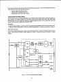


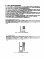

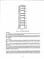


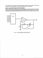


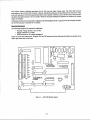


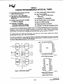


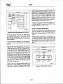

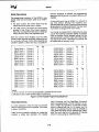


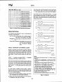
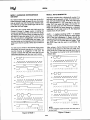


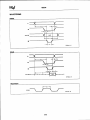


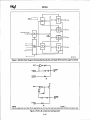
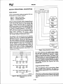


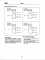
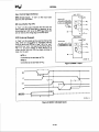

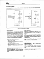


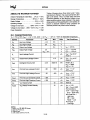


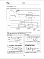


![PLAS A O ]-OR](http://vs1.manualzilla.com/store/data/005852706_1-5db0b7ed584537f0e62af161fb124638-150x150.png)