1
Real Time Trace Solution for LEON/GRLIB
System-on-Chip
Master of Science Thesis in Embedded Electronics System Design
ALEXANDER KARLSSON
Chalmers University of Technology
University of Gothenburg
Department of Computer Science and Engineering
Göteborg, Sweden, October 2013
The Author grants to Chalmers University of Technology and University of Gothenburg
the non-exclusive right to publish the Work electronically and in a non-commercial
purpose make it accessible on the Internet.
The Author warrants that he is the author to the Work, and warrants that the Work does
not contain text, pictures or other material that violates copyright law.
The Author shall, when transferring the rights of the Work to a third party (for example a
publisher or a company), acknowledge the third party about this agreement. If the Author
has signed a copyright agreement with a third party regarding the Work, the Author
warrants hereby that he has obtained any necessary permission from this third party to let
Chalmers University of Technology and University of Gothenburg store the Work
electronically and make it accessible on the Internet.
Real Time Trace Solution for LEON/GRLIB System-on-Chip
ALEXANDER KARLSSON
© ALEXANDER KARLSSON, October 2013.
Examiner: SVEN KNUTSSON
Chalmers University of Technology
University of Gothenburg
Department of Computer Science and Engineering
SE-412 96 Göteborg
Sweden
Telephone + 46 (0)31-772 1000
Cover: Picture of the GR-PCI-XC5V LEON PCI
Development board used in the project
Department of Computer Science and Engineering
Göteborg, Sweden October 2013
Abstract
Debugging real-time systems is often a time consuming process since they always behave differently
on real hardware than in an emulator. Aeroflex Gaisler has developed a complete SoC IP-library
together with a SPARC CPU. The existing trace solution for the CPU is only capable of storing a very
limited amount of debug data on chip.
In this project a trace system was developed that is capable of creating a trace stream, and then
transmit it over the high bandwidth PCI bus to a computer. Two different trace streams were
developed. The “Full” version contains all the execution information possible for every instruction.
The “Slim” trace version is designed for minimal bandwidth requirements. In order to achieve it an
efficient and complex encoding is used to log time information and execution path through the
program. However, the decoder requires that the trace binary is available when decoding the trace.
To further reduce the bandwidth efficiency the OP-code is not traced, since it can be looked op
afterwards in the binary. Arithmetic results are neither, but it might be possible to recreate those
with an advanced decoder/emulator solution.
~i~
Acknowledgements
I would like to thank my supervisor Jan Andersson and the staff at Aeroflex Gaisler for all the
invaluable help and support that they have given me. With their help I was never stuck for long. It
gave me plenty of time to work on the things which matters the most, which resulted in this project
being a success.
Many big thanks to my examiner Sven Knutsson for taking on this master thesis and for all the time
and effort he put into proofreading my report.
Finally, I thank my family and friends for all the moral support they have given me along the way.
~ ii ~
Abbreviations
AHB
AMBA
APB
CPU
DSU
FIFO
FPGA
FPU
GNU GPL
IP
JTAG
LSB
MSB
PC
PCI
RAM
SoC
TLB
VHDL
VHSIC
Advance High-performance Bus
Advanced Microcontroller Bus Architecture
Advanced Peripheral Bus
Central Processing Unit
Debug Support Unit
First In First Out
Field-Programmable Gate Array
Floating-Point Unit
GNU General Public License
Intellectual Property
Joint Test Action Group
Least Significant Bit
Most Significant Bit
Program Counter
Peripheral Component Interconnect
Random Access Memory
System on a Chip
Translation Lookaside buffer
VHSIC Hardware Description Language
Very High Speed Integrated Circuit
~ iii ~
Table of Contents
1
Introduction ..................................................................................................................................... 1
2
1.1
Background .............................................................................................................................. 1
1.2
Objective.................................................................................................................................. 1
1.3
Limitation................................................................................................................................. 2
1.4
Method .................................................................................................................................... 2
Theory and Tools ............................................................................................................................. 2
2.1
GRLIB ....................................................................................................................................... 2
2.2
LEON3 Processor ..................................................................................................................... 3
2.3
AMBA BUS ............................................................................................................................... 4
2.3.1
Masters and Slaves .......................................................................................................... 4
2.3.2
AHB Timing and Burst Transfers ...................................................................................... 4
2.4
Existing Trace and Debug Solution .......................................................................................... 5
2.4.1
3
4
Instruction trace buffer ................................................................................................... 6
2.5
PCI (GRPCI)............................................................................................................................... 7
2.6
FPGA Board .............................................................................................................................. 8
2.7
Xilinx ChipScope ...................................................................................................................... 8
Implementation ............................................................................................................................... 8
3.1
Brief Overview ......................................................................................................................... 9
3.2
CPU Instruction Trace block – Full Trace in Depth ................................................................ 10
3.2.1
RAW instruction registers .............................................................................................. 11
3.2.2
Packet Generators ......................................................................................................... 11
3.2.3
Generator Control ......................................................................................................... 12
3.2.4
Instruction Gen – Packet generator .............................................................................. 12
3.2.5
Trap Gen – Packet generator......................................................................................... 13
3.2.6
Shared Components ...................................................................................................... 14
3.2.7
Packaging of the stream ................................................................................................ 17
Trace Configuration and The Transmitter block............................................................................ 17
4.1
Trace Source Annotation ....................................................................................................... 17
4.2
AMBA Master ........................................................................................................................ 18
4.3
PCI Data Transfer Method ..................................................................................................... 18
4.3.1
Address mapping ........................................................................................................... 18
4.3.2
Trace Transmission Method .......................................................................................... 19
4.4
Clock and Transfer Speed Issue ............................................................................................. 20
~ iv ~
5
4.5
User Control Signals – Configuring the Trace Content .......................................................... 20
4.6
Trace Control Signals ............................................................................................................. 21
4.7
Verification ............................................................................................................................ 22
Slim Trace – Packet generator ....................................................................................................... 23
5.1
Program Trace ....................................................................................................................... 24
5.1.1
Tracing Direct Branch Instructions ................................................................................ 25
5.1.2
Tracing Indirect Branches Instructions .......................................................................... 25
5.1.3
Detecting the Direct Branch .......................................................................................... 25
5.1.4
Shared Component Signals & Changes made in Data Manipulation Blocks ................. 25
5.2
Program Trace with Precise Time .......................................................................................... 26
5.2.1
Small Cycle Packet ......................................................................................................... 27
5.2.2
Large Cycle Packet ......................................................................................................... 27
5.2.3
Break Cycle Packet......................................................................................................... 27
5.2.4
Packet Sequence Example ............................................................................................. 28
5.2.5
Shared Components Signals .......................................................................................... 28
5.3
Program Trace with Precise Time and Memory Data ........................................................... 29
5.3.1
6
Shared Components Signals .......................................................................................... 29
5.4
Trap Packet ............................................................................................................................ 30
5.5
Slim Trace Verification ........................................................................................................... 30
Evaluation and Future Work ......................................................................................................... 31
6.1.1
6.2
Bandwidth ..................................................................................................................... 31
Future Work and Shortcomings ............................................................................................ 31
6.2.1
Smaller Logic .................................................................................................................. 31
6.2.2
Full Trace ....................................................................................................................... 32
6.2.3
Improving the Slim Trace............................................................................................... 32
6.3
Software Developed & Usage Instructions............................................................................ 32
7
Conclusion ..................................................................................................................................... 34
8
Bibliography................................................................................................................................... 35
~v~
1 Introduction
A common technique used by software developers during debugging is to use print-line commands in
order to print debug information and find the errors in the software. In time critical applications it is
however unwanted to add debugging code to the software since it affects timing and the studied
issue might go away. Another possible scenario is that not enough data can be collected without
making the system miss its deadlines. For this reason specialized hardware is often integrated on
SoCs (System on Chip) that is able to trace both instruction execution and data bus transfers without
affecting performance.
1.1 Background
Aeroflex Gaisler [1] supports and develops an open source VHDL IP library, named GRLIB [2], which
contains the most important components for a SoC, like the LEON SPARC CPU [3], memory and bus
controllers, and communication controllers. The current trace implementation on the LEON CPU uses
on-chip memory buffers in order to store the systems trace data. The size of these memory buffers is
very limited because of area and cost restrictions, and since so much trace data is generated by the
CPU, even a large buffer would be filled instantly.
Although, it is possible to filter the trace in order to increase the running time it is unlikely that a
developer knows the exact origin of the fault, or when to stop the execution to prevent the useful
trace data to be overwritten. Therefore most often multiple attempts are required before the issue is
captured – making the debug process time-consuming. It has therefore been requested by customers
that this feature is improved on for the LEON CPU.
1.2 Objective
The goal of this project is to develop hardware that will allow a steady stream of trace data to be
captured and sent to a Desktop PC over the PCI bus, which provides a decent transfer speed and a
desktop computer provides good storage capabilities.
The hardware should be able to create a stream that contains full trace data, but also a slim
alternative needs to be developed that is better suited for systems that run in hundreds of MHz. Both
these alternatives will allow the whole execution of the program to be studied offline. Potentially
statistics of the execution could be extracted from the trace that can shed light on how well timings
hold etc.
The project should be conducted in such a manner that the end results could be reused for a future
production version. It is therefore required to produce a well thought through interface and
architecture that defines how trace data is to be collected, filtered, encoded and transmitted,
received and decoded on the desktop computer. The system specification should be designed so that
future trace devices can be designed later on without requiring major changes of this projects
outcome.
The solution should be made up by modular building blocks whose communication should not affect
the performance of the SoC. It is therefore required that the trace system operates on a separate bus
in order not to affect latencies on the main system bus. A central module should act as the
“collector” which controls the bus to which “trace generator” modules are connected. It should also
~1~
be possible to choose which modules to include, e.g. making the system-bus trace optional and
replaceable, and allow other transmission media other than PCI to be used.
A working implementation of the most important components should be implemented in hardware
and a working demo should be made that shows the features.
1.3 Limitation
Advanced software for processing of the trace data will be left out, but a simpler tool that is able to
decode the trace stream will be made. The reason for this being that a project of this scale could be
sized as a master thesis alone. E.g. writing a virtual debugger that can play back the trace stream will
not be done. Such a tool would allow a developer to use an IDE to step through the program offline.
When it comes to trace data generator modules only an instruction trace module will be created,
which probably also is the most complex module. The AMBA bus trace module may not be developed
in order to shorten the project, but the future implementation of it and multiprocessor support
should not require major re-engineering.
1.4 Method
The initial task is to research the existing solution in GRLIB and what solutions are already competing
on the market in order to discover useful features and implementation strategies that can be used
for this project, but also finding out what features and strategies that are less interesting.
The knowledge gathered will be used to write a complete specification for the components that will
and could be implemented. This is to ensure that a redesign of already developed components is not
required when new futures are going to be added in the future. The specification will cover how
trace data is gathered and annotated, and the transmission protocols used.
The key features like Instruction trace generators, a trace collecting module and a PCI transmitter will
be developed, simulated and tested in VHDL in ModelSim [4]. The software is fast enough to simulate
a complete system at around 1000 instructions per second. Overall only basic verification through
simulation will be done since exhaustive verification is not necessary for a non-critical component.
The PC software that will gather and store the data over PCI express will be implemented in C, but
the data presentation will be developed in a high level programming language if possible.
In the projects final stage the hardware will be implemented on a FPGA board, and suitable software
for demo will be prepared.
2 Theory and Tools
This chapter will attempt to capture and describe the fundamentals of the preexisting resources used
in this project. Any in-depth facts are brought up if needed where they are applied in the
Implementation chapters.
2.1 GRLIB
GRLIB is a complete IP Library which contains the resources needed to build a complete SoC design
and is provided by Aeroflex Gaisler. The main infrastructure of the IP Library is open-source and is
licensed under GNU GPL [3]. It contains a vast range of IP Cores as the LEON3 processor, PCI,
Ethernet, USB and memory controllers. A majority of these IP cores are connected to the central on
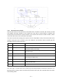
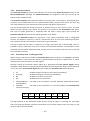
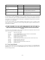
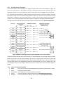
chip AMBA BUS [2] shown in Figure 1.
~2~
Figure 1: LEON3 system showing the AHB and APB bus Source: [2]
The IP Library is written in VHDL, and the provided Makefiles can generate simulation and synthesize
scripts for the most of vendors and CAD tools. The GRLIB is therefore portable across many
technologies.
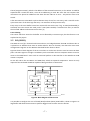
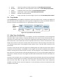
2.2 LEON3 Processor
The LEON3 is a 32-bit processor that implements the whole SPARC V8 specification [3], and it is
possible that a system has several LEON3 CPUs connected to the same AMBA bus.
The CPU has a vast range of configuration options and is easily configurable. The Trace Buffer, CoProcessor or FPU can be excluded from the design and the size of the caches and the register file is
easily changed. The TLB, which converts virtual to physical addresses, also has options for setting its
size and it is possible to share one TLB for both instruction and data addresses. A block overview of
the LEON3 processor is shown in Figure 2.
Figure 2:LEON3 block diagram. Source: [3]
The CPU has a seven stage pipeline. The stages are: Instruction Fetch, Instruction Decode, Register
access, Execute, Memory access, Exception, Write (back to registers). [3]
~3~
2.3 AMBA BUS
The AMBA 2.0 bus is the on-chip bus used in the GRLIB. It has the advantage that it is well
documented, does not have license restrictions and has a high market share since it is used by ARM.
Its specification contains three buses types: AHB (Advance High-performance Bus), ASB (Advanced
System Bus) and APB (Advanced Peripheral Bus). Using a bus with a high market share makes it easier
to reuse previously developed peripherals. In GRLIB only AHB and APB are used [2].
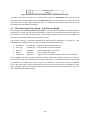
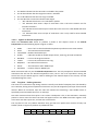
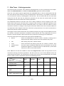
2.3.1 Masters and Slaves
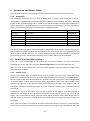
Figure 3 illustrates a small system that contains these two busses and devices attached to them. It
has been marked in the figure in italics whether a device is a bus master, which is capable of doing
transfers, or a slave that services a masters request.
Debug link
JTAG,ETH, Serial
master
CPU
master
High-bandwidth
on-chip RAM
slave
AHB
External Memory
Interface
slave
DMA bus
master
UART
slave
AHB /ABP
Bridge
AHB slave
APB master
APB
Keyboard
slave
PCI
master
(and slave)
Timer
slave
PIO
slave
Figure 3: shows masters and slaves and bridge of a common system
When a master requests a transfer it will be handled by the AHB BUS arbiter, which allows one
master access to the bus at a time. The AHB and APB buses are multiplexed and can therefore be
implemented on FPGAs, since they do not have the capability of leaving signals non-driven.
The APB Bridge which is connected onto the AHB Bus allows communication between the two buses.
The main advantage of APB devices is that they have a simpler protocol and a brief comparison
between the buses is made in Table 1. As default the APB Bridge is placed on address 0x80000000
inside the LEON3 system.
AHB capabilities:
APB capabilities:
Data bus width of 32/64/128/256 bit
Non-Tristate implementation
o Useful since it is not available
on all technologies
Burst transfers
Single cycle bus master handover
Data bus width up to 32 bit
Low power
Simple interface
o Smaller logic
No burst transfers
o Suitable for devices requiring
less memory bandwidth
o Devices are only slaves
Table 1: Comparison of AHB and APB. Source: [5]
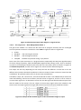
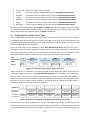
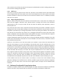
2.3.2 AHB Timing and Burst Transfers
Since the PCI bus will be used to transmit the trace stream, the AHB must be used for maximum
performance. Figure 4 is a time diagram which will be used to explain how AHB data transfers are
performed by one single bus master.
~4~
An AHB bus transfer consists of a one cycle address phase followed by at least one cycle data phase.
The most basic example of this is transfer A. During this transfer’s data phase the HREADY signal is
immediately driven high, and comes from the currently accessed slave which signals that it is ready
to receive the data. During the data phase of transfer A it is already possible to start the new address
phase of B, since HREADY indicated that A transfer is OK.
However, during the first data phase of B the slave responds that it is not ready, and the master
holds the data signals until it is. As seen, even though the slave signals it is not ready the address is
allowed to change to C. Therefore the slave must remember the B address until it can store the data.
Addr phase A
Data Phase A
Addr phase B
Wait phase B
Data Phase B
Addr phase C
Data Phase C
HCLK
HADDR
A
B
C
Control
Control
A
Control
B
Control
C
Data A
Data B
HWDATA
Data C
HREADY
Figure 4: shows how multiple transfers simultaneously transmit data and the next address
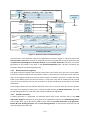
2.4 Existing Trace and Debug Solution
The existing trace solution is integrated in to the LEON3 processor and the DSU (Debug Support Unit),
which is an AHB slave connected to the systems AHB bus. The instruction trace is generated and
stored inside the processor and the AMBA bus trace is generated and stored in the DSU.
It is possible to set breakpoints in the DSU in order to halt the CPU when it reaches a certain
instruction in the program or halt on a certain AHB bus transfer. On a halt the system will enter
debug mode in which it is possible to read registers in the CPU, the cache and trace buffer from the
LEON3 processor.
The DSU is accessed by a Debug Host Computer connected to the system through one of the many
possible IO alternatives like JTAG, Ethernet or even PCI (shown in Figure 5). These IO devices are AHB
masters and have the ability to perform bus operations on the Debug Host Computer’s request. A
program called GRMON, a debug monitor running on the Debug Host, allows the user to control the
DSU and do other read and writes on the AMBA bus.
~5~
Figure 5: Connection between CPU-DSU-I/O and Debug Host. Source: [3]
2.4.1 Instruction trace buffer
The DSU has access to the Instruction Trace Buffer that is located in the CPU and contains an AHB
Trace Buffer that logs transfers on the system bus. One entry in these buffers is 128 bits and
corresponds to one instruction (or bus transfer). The content of the entries is listed in Table 2, which
is the main data source in the real-time trace system.
The main issue with the existing trace system is that on chip RAM is costly. The amount that can be
used for storing the trace is limited to just a few kilobytes, and therefore when the buffer gets full
the oldest entry has to be overwritten.
Bits
Name
Definition
127
(Unused)
Rounds the entry to nearest byte
126
Multi-cycle instruction
Set to ‘1’ on the second and third instance of a multi-cycle
instructions (LDD, ST or FPOP)
125:96
Time tag
The value of the DSU time tag counter. It increments by one
each clock cycle.
95:64
Load/Store parameters
Instruction result, Store address or Store data
63:34
Program counter
The address of the executed instruction (2 lsb bits removed
since they are always zero)
33
Instruction trap
Set to ‘1’ if traced instruction trapped
32
Processor error mode
Set to ‘1’ if the traced instruction caused processor error
mode. The CPU stops.
31:0
OP-code
Instruction OP-code
Table 2: Instruction Trace Entry. Source: [3]
The Time Tag is a 30 bit value and is used to get the delay between instructions execution. It is
generated from a counter which increments by one each clock cycle, but is paused when the system
enters debug mode.
~6~
The PC (Program Counter), which is the address of the executed instruction, is also 30 bits. It could be
expected that it would be 32-bit, since 32 bit addressing is used. But since the CPU requires that
instructions are placed on addresses that have the two LSBs set to zero – only 30 bits have to be
stored.
A few instructions use the Multi-cycle bit because they do not fit in one entry, and is used for multicycle instructions. If the bit is high the entry is an extension of the previous entry.
Every entry in the trace buffer has 32 bits reserved for the result. But, if e.g. an LDD (Load Double) is
executed, two trace entries are made, and if a STD (Store Double) is executed one entry is used for
the accessed address and two entries for data. [3]
Trace Filtering
The entries which are stored in the buffer can be filtered by instruction type, but this feature is not
explored in this project.
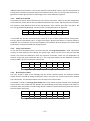
2.5 PCI (GRPCI)
The GRPCI IP core [3] is licensed under GPL and acts as a bridge between the AHB and the PCI bus. It
is placed on an AHB bus that must be 32-bit wide for burst to function, but does also have some
configurations registers on the APB bus described further down in detail.
Figure 6 shows a block diagram of the IP core where it can be seen that the core has two main data
paths. The PCI Target on the right is mandatory and is used when the host computer wants to read or
write to the FPGA board. Since such an action will perform a data transfer on the AHB bus an AHB
master is required.
On the left side is the PCI Master and AHB slave, which are optional components. These are only
required if the PCI board should be capable of doing transfers on the PCI bus.
AHB
APB
GRPCI
APB Config Registers
AHB Slave
Ma Rd
FIFO
Ma Wr
FIFO
AHB Master
T Rd
FIFO
PCI Master
T Wr
FIFO
PCI Target
PCI bus
Figure 6: Block diagram of the PCI core
It is possible to configure the size of the Rd (Read) and Wr (Write) FIFO buffers, shown in Figure 6. A
large buffer will allow the PCI mater to perform bigger burst transfers over the PCI bus.
~7~
2.6 FPGA Board
The development board used is a GR-PCI-XC5V [6] and has a Virtex-5 XC5VLX50 FPGA from Xilinx on
board. The development board was specially designed for LEON systems, and its primary feature is
the PCI connector that is running at 33MHz with a data width of 32-bit. It can thus be a regular PCI
card for desktop computers. [6]
Other significant features of this board are:
Gigabit Ethernet Controller
USB 2.0 including both host and peripheral interface
80 Mbit onboard SRAM
128 Mbit onboard FLASH PROM
One SODIMM slot for off the shelf SDRAM (up to 512MByte)
2.7 Xilinx ChipScope
During development Xilinx ChipScope [7] was a very helpful tool. It is a logic analyzer that can be
included onto the FPGA, and it can trace any signal that exists in the VHDL design [7]. It is used for
debugging the hardware which otherwise would be a very complicated task.
ChipScope collects the signal states in full speed onto a small memory. E.g. 128 signals with 2048
samples will require 128 × 2048 = 262 144 kb (32kB) on chip memory. When the memory is full
ChipScope stops the data collection, transfers the data over JTAG to the computer and shows it as
waveforms.
If it is whished that ChipScope should log the value of a new signal, almost the whole hardware
synthesis has to be redone, in order to forward the signal to the ChipScope module. The re-synthesis
takes 20 to 30 minutes, so the debugging process easily takes long time before the issue is found.
3 Implementation
This chapter focus will on how the full version of the Real-Time trace is implemented, which includes
as much information as possible. The slimmed down version will be presented in chapter 5 instead,
after the basics have been covered.
The Real-time trace solution reuses the existing trace generation of the LEON3 CPU by breaking out
the signals which are intended for writing into the trace buffer memory. The trace entries (shown in
Table 2) contain a satisfying amount of information and it is therefore not needed to develop a
custom solution that extracts data from the integer pipeline.
The CPU Instruction Trace block detects that the Trace Buffer Input Data is valid when Trace Buffer
Write Address changes and when its write enable signal is high. This indicates that the CPU wrote a
trace entry and increased the write pointer to the address where the next trace entry shall be
written.
~8~
Ethernet
Debug Link
Trace
Buffer
AHB main
Bus
LEON3 CPU
Real-time
Trace collecting
Desktop Computer
Memory
Controller
GR PCI controller
Trace Buf
Write Addr
Trace Buffer
Input Data
PCI
BUS
AHB/APB
Bridge
AMBA Trace
bus
master and slave
FIFO
Buffer
APB config registers
Transmitter
Trace
APB
AHB master
Data
AHBRAM
Trace Function
APB
slave
Ctrl. Reg.
settings
Trace Data
23 or 31 Byte
Instruction
Trace Generator New Data
Recieved
JTAG / Serial
Debug Link
Trace Control Signals
master and slave
With FIFO state (Overflow)
Non Real-time
Trace collecting
Computer
Slow
Link
Figure 7: A trace system component overview. Dotted connectors are virtual signals. Dashed boxes
are components used during early data transfer before PCI functionality.
3.1 Brief Overview
The CPU Instruction Trace block will generate a trace stream that the developer has selected. There
are two possible Trace Streams implemented but this chapter is dedicated to describe the full trace
stream. It consists of mostly Instruction Packets with variable lengths, as shown in Figure 8. Packets
always have one byte header which specifies type of data and how much of it that follows.
Instr.
Header
Prog. Count.
1-5 Byte
Time Tag
1-5 Byte
OP code
4 Byte
Result
4/8/12 Byte
Figure 8: A variable length Instruction Packet used during full trace
The instruction packets that are 23 or 31 bytes long are then fed into the Transmitter over the Trace
data bus. Multiple instruction packets can fit in one transfer and may overlap two transfers as shown
in Figure 9. The size of the Trace Data bus is configurable and choosing a smaller bus will result in less
hardware logic, but the bandwidth might be less suitable if multiple trace data sources exist, e.g. a
multiprocessor system.
Transfer 1
Instruction 1
Transfer 2
Instruction 2
Transfer 3
Instr. 4
Instruction 2
Instruction 3
Instruction 4
Instruction 5
Figure 9: Illustration how transfers can look like on the Trace Data Bus
The Transmitter block will then encapsulate this data with one byte Frame Header that contains the
generation source of the trace data, creating a 24 or 32 byte frame for transmission (Figure 10)
depending on the Trace Data bus width.
~9~
Frame
Header
Trace Data Transfer
23/31Byte
Figure 10: Illustrates how the frame header encapsulates the stream
The frame will then be stored in an internal FIFO inside the Transmitter block before it gets
transmitted over the dedicated 32-bit wide AHB Trace bus. It is only used for the real-time trace so
that performance of the original LEON3 system bus is unaffected. The PCI unit then writes the trace
into RAM of the Host desktop computer.
3.2 CPU Instruction Trace block – Full Trace in Depth
The main goal of the CPU Instruction Trace block is to encode the trace buffer entries generated by
the CPU into a stream. All the existing information is used in the stream generation except the error
bit because it is rare and it stops the CPU. The information about the error in the Trace Buffer is
therefore not overwritten before the user gets to read it.
The streams content is selectable depending on what data the developer is interested in. The
following data is included in the full trace and some are selectable by the user.
PC Address
Time Tag
OP-code
Result
Trap Packet
(mandatory)
(mandatory)
(optional)
(optional)
(always on)
– address of the executed instruction
– time that the instruction executed
– 4 byte specifying the instruction
– 4, 8 or 12 Byte result data
– registers if the instruction caused a trap or was interrupted
The PC Address and Time Tag are mandatory because the decoder software requires it in order to
even start decoding. These restrictions do however not exist on a hardware level and the user could
e.g. disable the PC Address, but in most cases a trace without it is not particularly useful. In addition
the PC and Time Tag are often compressible to one byte and it was therefore reasonable to leave
them mandatory. But the OP-code and Result are not compressible and the Trap Packet is very rare
and is therefore left always enabled.
~ 10 ~
Shift on
Data
M=0 => new
Instruction.
RAW instruction registers
M TimeT L/S R/A
PC TE OP
M
R2
M
R1
M
R0
Raw reg
Generator Control
Raw reg
Packet Generators
Low Prio
High Prio
Trace Control
Signals
Trap gen
Branch &
Cycle &
Data gen
Inst gen
Sync Packet
Intervals
and management
forceFlush
Shared Components
Data
Manipulation
Blocks
White space
removal
Head
Head
byte
11byte
BRPC
BR Addr 0-5 byte
PC 0-5
TT
TimeTag 0-5 byte
Left Shifter 10bit
BRRes
BR TimeTag 0-5
L/S R/A 0/4/8 byte
Left Shifter 5+8 bit
Left Shifter 11+10 bit
Insert en
Data
forceFlush
BROP
BR Addr 0-5
OP 0/4 byte
InsertEn
Size
Aligner Block (Rotator) Tbus wide register
Out Out
0 (1+5+5+4+8
Bus (23 B wide)
= 19 B )
Figure 11: CPU Instruction Trace Block diagram
The Instruction Trace Generator consists of multiple blocks, shown in Figure 11. The Front end of the
CPU Instruction Trace block consists of components that control what packet is generated. These are
the RAW Instruction Registers, Generator Control and the Packet Generators. However, the actual
generation of the packet is only done in the Shared Components block. All these sub-blocks are
covered in detail in the following subsections.
3.2.1 RAW instruction registers
The RAW instruction registers will hold the latest three trace entries from the CPU’s Trace Buffer.
Each entry contains the data that was listed in Table 2. The reason for having three trace entries is
that it is the largest amount that any instruction requires, as stated in section 2.4.1. When the trace
buffer write address (from the CPU) increments, a new trace entry will be shifted into R2 and the
entry at R0 is evicted. By this time the instruction in R0 has already been processed by the Packet
Generators.
The R0 register does have one extra bit called the “fresh” bit. It is used to make sure that the content
that stays in the register for many cycles is only processed once by the Packet Generators. The fresh
bit will always flip low one cycle after new content is shifted into register R0.
3.2.2 Packet Generators
A packet generator is responsible for detecting when there exists relevant data in the RAW
Instruction Registers and based on that generate an appropriate input for the Shared Components
and a header byte, e.g. an Instruction Header. There exist three Packet Generators: Trap generator,
Branch & Cycle & Data generator and the Instruction generator. In the full trace only the trap and
instruction generators are used.
~ 11 ~
3.2.3 Generator Control
The Generator Control is the unit that will grant one of the three Packet Generators access to the
Shared Components. Although, the Packet Generators are designed so that two of them do not
request access simultaneously.
The Generator Controls most important feature is to ensure that a Sync Packet is transmitted when
necessary. A Sync Packet does not use a special packet header, but just leaves the PC and Time Tag
non-compressed once. This means that the PC and Time Tag will use 5 bytes each.
The Sync Packet allows the stream to recover or resume from it in case an error occurs. The most
likely error that requires a Sync Packet for recovery is an overflow in the Transmitters FIFO. When
this occur all packet generation is suspended until the FIFO is empty again. Upon resume the
Generator Control will make the first packet generate a sync packet.
However the Generator Control also generates a sync packet periodically with a configurable
interval. This allows for recovery in case of a transmission error or if the Trace Collecting Computer
was unable to save the trace stream in time before it got overwritten.
The Sync Packet will also allow a subsection of a large saved trace file to be decoded, and it is
possible to input a subsection of the trace stream into the decoder software. The usefulness of this
periodical synchronization might be limited, but the stream size increases with less than 1% and the
cost is therefore minimal.
3.2.4 Instruction Gen – Packet generator
When tracing in the full trace mode the Instruction Gen (shown in Figure 11 as Inst gen) is the main
Packet Generator. A new instruction packet is generated when the M bit in register R0 is ‘0’, which
indicates that a new instruction is in that register.
However, before an Instruction Packet (Figure 8) is generated the Trace Control Signals will be
checked for what dataset is requested by the developer and the appropriate flags in the Header byte
are set. The list of Trace Control Signals that are used by the Instruction Gen are listed below.
PC
– Enables Program Counter for instructions (mandatory)
TimeTags
– Enables TimeTag for instructions (mandatory)
OP
– Enables OP-code for instructions
Res
– Enables Result for instructions
fifoThreeQuarter – The FIFO in the Transmitter is 3/4 full. Removes Result and OP-code to
avoid Overflow.
fifoFullHit
– The FIFO in the Transmitter is or was full. Disables the Instruction Gen
until FIFO is empty.
7
6
5
4
3
2
1
Res(1) Res(0)
TT
PC
OP
1
1
Figure 12: Header byte for an Instruction Packet
0
0
The flags positions in the instruction header byte are shown in Figure 12. The flags are active high
and are used by the decoder software to find where an Instruction packet starts, how long it is and
where to expect the next header.
~ 12 ~
The OP bit indicates that the OP-code is included in this packet
The PC bit indicates that the Program Counter is included
The TT bit indicates that the Time Tag is included.
The two Res bits are used to indicate result length.
o “00” indicates that there is no result data in packet.
o “01” indicates there exists 4 byte of result data. This is the most common size for
normal instructions.
o “10” indicates there exists 8 byte of result data. This occurs for Load double and Store
instructions
o “11” indicates there exists 12 byte of result data. This is only used for Store Double
instructions.
3.2.4.1 Signals to Shared Components
When the Instruction Gen wants to produce a packet it will request access to the Shared
Components and the following inputs are given to them.
Mode
Head
CancelHead
Enable
BrPcNew
TTNew
BrOpNew
Result
ResultSize
– Set to “00” so that the Shared Components produce an Instruction Packet.
– The Instruction Packet header
– Disables the header byte
– 4 bits that enable or disable output for PC, Time Tag, OP-code and Result.
– Is set to the Program Counter.
– Is set to the instructions Time Tag.
– OP-code of the instruction.
– The Instruction result. MAX 8 byte.
– number of bytes. MAX 8 byte.
Most instructions will only use the Shared Components once. The only exception is the Store Double
Instruction that will use the Shared Components twice, since it has a 12 byte Result. During the
second use only the Result signal is used for adding the last 4 Result bytes to the stream, and the
CancelHead signal is active.
3.2.5 Trap Gen – Packet generator
The cause of an instruction trap during runtime is usually some kind of exception/error like divide by
zero. However, during normal operation instructions may also be trapped by interrupts from external
devices. When an instruction traps the CPU will instead start executing a trap handler which is
specifically aimed to handle that error or interrupt.
One other occasion when the trap bit is set is when a breakpoint is hit, or the execution is manually
paused. In these cases the same instruction will appear twice in the RAW instruction registers. One
occurrence with the trap bit set, and one with a valid result.
The trap bits are set very seldom therefore they get their own packet that consists off only one
header (shown in Figure 13) without any additional data.
7
0
6
5
4
3
2
1
0
1
1
1
1
1
Figure 13: Header byte for an Instruction Trap
~ 13 ~
0
1
When a trapped instruction is shifted down to register R0 in the RAW instruction registers a regular
Instruction Packet is generated first. Since the Shared Components are busy generating the
Instruction Packet the Trap Gen always delays its request one cycle. The Trap Header is therefore
telling that the previous instruction in the stream was trapped.
Since the Trap Header is delayed one cycle there is a small risk that the Trap bit is lost if a new
instruction is immediately shifted into register R0. In this case the Instruction Gen request has a
higher priority. However, no instruction packets will be missing from the stream, and it will be seen
that the trap handler started to execute even if the Trap Packet was dropped. This problem was not
realized until after the design was considered finalized.
If the error bit is set it means that the CPU entered the error mode because of that instruction and
stops execution. This error bit is not handled by this solution, but since the CPU is halted on errors
the existing trace implementation is sufficient to find the error.
3.2.6 Shared Components
The Shared Components will assemble a packet depending on what input data is given to it. Since
these components are shared some hardware does not need to be duplicated when the Slim Trace is
implemented. The largest area savings are made on the various shifting logic and Aligner Block which
are shown in Figure 14. The Shared Components consist of:
Multiple Data Manipulation Blocks which are able to compress data or leave it unmodified.
Each Data Manipulation Block has out signals for data and data length.
The White Space Removal section merges the data from the Data Manipulation Blocks into
a contiguous instruction trace packet by using multiple shifters.
A Bus transfer Aligner Block allows multiple instructions to share one transfer to the AHB
Transmitter block, as illustrated in Figure 9
Registers for storing the previous PC address and Time Tag (not shown)
The in-signals to this block were already covered in Signals to Shared Components. In order to tell
the Shared Components block what packet it should generate a two bit Mode signal is used. “00” is
used to create Instruction and Trap Packets while the other combinations are used for the Slim Trace.
When the Slim Trace was implemented additions were also made to the Data Manipulation Blocks,
but this will be covered in the next chapter.
~ 14 ~
BrPcEn
PreBits(1:0)
BrPcMode
Head 1B
Data
Manipulation
Sub-Blocks
TTEn
BrPcNew (31:0)
BrPcOld(31:0)
Head
1 byte
Head
1 byte
Left Shifter 5+8 bit
Data length (3:0)
Data 0-12 B
Data length (3:0)
Left Shifter 11+10 bit
Data length (4:0)
Data
Bus transfer
forceFlush
alignment
Data length (3:0)
Insert en
Data 0-5 B
Left Shifter 10bit
Data 0-10 B
TtRes
BR TimeTag 0-5
L/S R/A 0/4/8 byte
Data length (2:0)
Data 0-5 B
Data length (2:0)
Data 0-5 B
White space
removal
TtResNew (63:0)
TtResOld (31:0)
BrOp
BR Addr 0-5
OP 0/4 byte
TT
TimeTag 0-5 byte
Data length (2:0)
Data 0-5 B
Insert en
BrOpMode
BrOpNew (31:0)
BrOpOld (31:0)
TTNew (31:0)
TTOld(31:0)
BrPc
BR Addr 0-5 byte
PC 0-5
ResultSize(3:0)
TtResEn
TtResMode
BrOpEn
Aligner Block (Rotator) Tbus wide register
To Bus/FIFO
Figure 14: Shared Components block diagram. In signals in blue
3.2.6.1 PC compressor – Data Manipulation Block 1
The goal of the module is to remove the bits from the PC (Program Counter) that are unchanged
since the previous instruction. The block is named BrPc in Figure 14 and its in-signals are:
Enable
BrPcNew – The new Program Counter
BrPcOld – The old Program Counter
CompOff – Disables compression during “sync packets”
Since most of the time instructions in a program execute sequentially the LSB (Least Significant Bits)
of the PC change frequently, while the MSB (Most Significant Bits) change rarely. There is therefore
no point in transmitting the stationary bits over and over. The old PC, which is stored in a register in
the Shared Components, and the new PC signals are used to find the differentiating bits.
The output size will vary depending on how many bits that are different. If seven bits or less are
different only one byte data will be produced. It does not matter if there are three or seven bits that
are different. All seven bits will be set as if all seven bits were different.
The MSB in a byte, the “continue bit”, will tell the decoder if there is one additional byte with seven
more bits following. This last bit is shown in the left column in Figure 15, and if it is set to 0 there is
no more data. Figure 15 is an illustration of how the out data signal will look like when 3 bytes of PC
data are added to the stream. The last 2 bytes of the out data signal will not be included in the
stream since the output signal Data Length will tell that only the first 3 bytes should be included.
1
PCData 6:0
1
PCData 13:7
0
PCData 20:14
0
PCData 27:21
0
PCData 31:28
Figure 15: Example of the out-data signal. In this case the Data Length is 3 byte.
~ 15 ~
3.2.6.2 Time Tag compressor – Data Manipulation Block 2
The time tag compressor is identical to the BRPC compressor in its function and applies the same
compression, by using the old and the new time. The compression method is suitable since the Time
Tag also counts upwards, and will usually have a value that is slightly higher than it was in the
previous packet. The average size of the Time Tag will therefore be just above 1 byte per instruction,
only exceeding one byte when more than the seven LSB change.
3.2.6.3 Choosing the Compression method and limitations
The chosen compression encoding scheme is more efficient than having a value in the stream
representing the amount of bytes that are being transmitted. If done so 3 bits would always be used
to indicate the PC length of 0 to 4 bytes. However most of the time only one byte is used for the PC
and this encoding will only use 1 bit to indicate the data length.
The encoding does have a drawback. For example, if a program executes a loop which has its first
instruction at address 0x0FF0 and the last at 0x1004, the MSB would switch often. Every time the
address shifts from 0x0FFC to 0x1000 and from 0x1004 to 0x0FF0 the instruction address requires 3
bytes.
3.2.6.4 OP-code – Data Manipulation Block 3
The OP-code block is either enabled or disabled and can place the 4 byte OP-code into the trace
packet. There is no OP-code compression available on this block. Although it is possible to implement
compression logic which substitutes frequently executed OP-codes with small code-words, it is
doubtful that it is worth the additional hardware and the effort to develop it. The compression
efficiency would be highly dependent on if the same operations are used frequently and the OP-code
for adding register A and B would be different form adding register B and C.
After all implementing compression serves little purpose since the OP-code can later be looked up in
the program binary when the trace stream gets analyzed. An exception would be if the program is
intentionally or un-intentionally modified during runtime on the LEON3 system.
3.2.6.5 Result – Data Manipulation Block 4
The result block can forward up to 8 byte data. The valid data size is set by the Result Size signal. The
Mode signal will control if is outputting unmodified data (or is in a compression mode for the Slim
Trace).
3.2.6.6 Whitespace removal
The whitespace removal section concatenates the PC, Time Tag, OP-code and Result data into one
contiguous packet by performing a series of byte shifts. In total there are three Left Shifter units,
shown in Figure 14.
1. Shift Time Tag over PC
2. Shift Result over OP-code
3. Shift the second over the first.
For example the last two bytes in Figure 15 would be shifted over by other data from Time Tag, and is
performed in the 10 byte Left Shifter.
~ 16 ~
3.2.7 Packaging of the stream
After the creation of an instruction trace packet it is fed into the Aligner block. The task performed
by this block is to merge the instruction trace packets into a stream where there are no bytes lost
due to padding. The data out of the Aligner block could contain the end of one trace packet and
contain a complete packet as shown in Figure 9.
4 Trace Configuration and The Transmitter block
The trace transmission hardware is placed on a separate AMBA bus in order not to affect the original
LEON3 system. For transmission and configuration of the Trace stream the GRPCI IP-core (covered in
section 2.5) is used, which is left at the default configuration that was set in the build directory for
the GR-PCI-XC5V FPGA-board.
Since the Trace system uses an ordinary AMBA bus, the transmission is not limited to just PCI, but it
would be possible to transmit or store the trace stream on any AMBA slave, like ordinary SDRAM
through a DDR Memory Controller. E.g. during early development a 16kb AHBRAM memory (part of
GRLIB) was attached to the Trace AHB for storing the stream on the FPGA, shown in Figure 7 as
dashed blocks. The stored trace was then extracted over a debug link, and its correctness was
verified before adding PCI support and other features.
PCI is the most suitable transmission medium. Media such as Ethernet or USB were considered, and
are available as AMBA devices, but were disregarded. The Ethernet IP core requires advanced control
to form packets and is therefore better suited for software control. USB 2.0 on the other hand has
too low performance. If the PCI would not have been used the trace stream could first have been
stored on regular DRAM before transmission over USB. This latter method allows to do a full trace for
a few seconds if a PCI FPGA board is not available.
4.1 Trace Source Annotation
The data that arrives from the Instruction Trace Generator block (Figure 7) is done so over the Trace
Bus which is configurable to either be 23 or 31 byte wide. The reason the bus has an odd width is to
make room for one extra byte, called the Frame Header. It contains the source id of the device which
created the trace data in order to be able to identify trace streams from different CPUs. However,
multi-CPU support was never implemented because the logic required did not fit on to the FPGA, and
neither was the AMBA trace unit developed. Thus the trace stream does currently only contain the
trace from one source (the CPU). After the Frame Header has been created it is merged with the
incoming data to create a Transfer Frame (shown in Figure 10). It is then temporarily placed in a
FIFO-buffer inside the Transmitter before being transmitted. Having a 6 kB buffer seemed to be
enough.
The Frame Header byte is specified to have the format shown in Figure 16. There are four source bits
which make it possible to distinguish trace data from 16 devices. The overflow bit is set high if there
was previously an overflow. This means when the fifoFullHit signal (section 4.5) from the Trace
Control Signals goes low, the first Transmission Frame will have the Overflow bit set.
7
6
5
4
3
2
1
0
Src(3) Src(2) Src(1) Src(0)
0
0
Overflow
1
Figure 16: The Frame Header byte which contains the trace source
~ 17 ~
Since the length of the frames transmitted is always the same, the transmission frames will always be
24 or 32 Bytes apart. This is used by the decoding software to find the frames.
4.2 AMBA Master
In order to be able to transmit data to the PCI slave an AHB Master had to be developed. The Master
will first read 24/32 byte sections from the FIFO where the trace is temporarily stored and then
transmit the data to the PCI unit in a burst. In order to achieve maximum performance these bursts
have to be long. 6 bus-transfers (24 Byte) bursts resulted in a transfer speed of only 35-40 MB/s, but
reached 80MB/s if infinitely long bursts were supported.
The development of this unit took a significant time before the transfers were reliable. First of all it
took some time to get basic burst write transfers working to the AHBRAM IP-core. But the main
challenge was to build a working state machine that can respond to the PCI unit’s ready signal
(problem illustrated in Figure 4). The reason why this was complicated was that there exists no good
known IP-core that can be used to simulate the AMBA Masters retransmission functionality.
The only way to test the AMBA Master was to synthesize the whole system and make a test run,
which is very time consuming. In order to get his right and find the errors ChipScope was used.
However, eventually the AMBA master only missed a transmission every 10-50kB, which is too rare
to efficiently capture the problem whit ChipScope, since it also stores the debug data on the FPGA
before transmission. But in the end the last issue was also resolved.
4.3 PCI Data Transfer Method
The PCI IP-core can write anywhere in the desktop computers RAM. Part of the RAM on the
computer is reserved where the Trace system writes its data. The easiest way to reserve memory on
Linux is by limiting how much memory the OS is allowed to use. This is done by passing the kernel
boot parameter “mem”. Since the Computer used for the Trace Collecting had 2048 MB RAM setting
“mem= 1792M” (1.75GB) will leave top 256MB memory unused for a Circular Buffer (Figure 17).
However not all the memory needs to be used e.g. 48MB was sufficient during tests, but if the hard
drive where the trace is saved has uneven performance a larger buffer might be required. Since the
trace is transmitted in 24 byte frames the circular buffer size has to be a multiple of 24 bytes, like
48MB.
The “mem” boot parameter method will not work if more than 4GB of RAM is ever needed on the
desktop computer. In order to use more RAM a kernel module has to be compiled into the kernel
that can reserve a contiguous memory area below the 4GB mark at boot time.
4.3.1 Address mapping
Before the Trace System can transmit the PCI device has to be configured. This is done during
initialization when the trace saving software is started on the host desktop computer. During
initialization the trace options that were chosen by the user are transmitted, and the memory
mapping is set so that the trace system transmits the trace to the correct RAM address. If the
memory address where to store the trace is not properly set the desktop computer will most likely
crash and reboot.
Within the Trace AHB bus the PCI Master (AHB slave) is mapped to address 0xE0000000 –
0xEFFFFFFF, which is a 256MB address space. This address space can then be mapped to an
equivalent block inside the Host Computers RAM, e.g. between 1.5GB and 1.75GB or 1.75GB and
~ 18 ~
2GB. This mapping is done during initialization of Trace System, when also the Trace Stream
configuration that was chosen by the user is set.
Trace System
Address Space
Host Computer
Address Space
0xE0000000
0x70000000 = 1.75GB
Circular buffer In
Host Computers
Main Memory
48MB-256MB
suggested
0xE3000000
0x73000000 = (1.75GB + 48MB)
Figure 17: Shows the 256MB in Desktop Computers RAM which may be written too.
On a regular Linux distribution for x86 physical RAM is mapped from address 0x00000000 and
upward, therefore the 1.75GB mark in the desktops memory is located at address 0x70000000.
In order to do setup correct memory mapping only the first configuration register of the PCI core
needs to be modified. It is located on the APB bus where there are 4 bits which tell where the 256MB
block is mapped. In this case they are set to 7.
When this is done any writes that are done to 0xE00000000 on the trace AHB will be transferred over
PCI to the Trace Collecting Computers memory at memory addresses 0x70000000, as shown in Figure
17.
4.3.2 Trace Transmission Method
The Transmitter unit will start writing on a set start address (0xE0000000) and will continue to write
until it reaches the loop address (0xE3000000). When the loop address is hit it will stop the write
burst and then go back to start writing from the beginning (0xE0000000). It will continue to write into
memory in a circular manner until the tracing is stopped.
The software on the desktop computer will extract and store the trace stream as soon as possible.
During startup the reserved memory is completely cleared with zeroes. When the Trace System later
starts writing into the memory the software detects the new data since the memory is no longer
cleared. This new unread data is illustrated in Figure 18. If the “Software read location” catches up to
the “Trace Hardware write location” the software will stay in busy wait loop. While the software is
waiting it will look 64 bytes ahead in memory searching for non-cleared bytes.
Read and Cleared
data by Software
Data not read by
Software yet
Software read
location
Trace Hardware
write location
Data was read and
cleared on the
previous loop
Figure 18: Shows how the HW writes pointer is ahead and the SW tries to keep up storing to disk.
The read progress is slightly behind.
~ 19 ~
After a memory location has been read it will always be cleared. When the software loops around
the reserved memory area the next time, it will check if the memory location is still cleared. If it is, it
will do a busy wait until new data has been written to that location.
The Transmitter will not verify that the Software on the Computer actually did read and store the
stream, since that would increase communication and decrease transfer speed. If the storage device
on the Computer is too slow there will be an overflow in the Circular Buffer and part of the stream
will be overwritten.
An overflow would anyways be unavoidable even if communication for verification existed since the
FIFO on the FPGA is so small in comparison to the Circular Buffer in RAM. The major advantage if
overwrites were detected would be that it becomes possible to handle the overflow by stopping the
trace and transmit a Sync Packet. However the trace already includes periodical Sync Packets so it is
already technically possible to recover the trace stream.
However the recovery has to be done manually for this kind of overflow, since the software is not
capable of removing the broken part of the stream and will likely crash. It is likely that the software
mistakenly uses e.g. the OP-code or Result as a Packet Header. Almost every possible 8-bit
combination is used in the “Slim Trace” header.
4.4 Clock and Transfer Speed Issue
It is important that the user selects to trace a feasible amount of data and sets the clock speed of the
system appropriately. Otherwise, there will be gaps in the stream when the PCI controller is unable
to keep up, resulting in that some trace data is lost.
During development it was realized that GRPCI version 1 core only supports 32 bit (4 byte) transfers
per cycle, but in the worst case 11 bytes Instruction Packet could be generated each cycle.
Since it was not possible to solve the bandwidth problem by increasing the AHB bus width, the AHB
Trace bus was clocked four times faster than the LEON3 CPU and its bus. This was achieved by
dividing the clock of the original LEON3 system by four. Unfortunately the built in clock dividers on
the FPGA could not deliver a clock speed lower than 32 MHz, which would have resulted in a trace
stream around 300MB/s – way above the theoretical 133MB/s of PCI.
Therefore a less desirable solution was made with a counter that counts up to four and generates a
pulse on loop-over that was instead used as the LEON systems main clock. With the previous main
clock at 40 MHz connected to the trace system, the LEON system got a 10 MHZ clock. A full trace
stream would then average on 80MB/s with everything enabled without overflows.
Because the Trace System was clocked faster than the CPU system, the issue where the Trap Packet
request for the Shared Components was canceled by the Instruction Generator was never detected
during testing.
4.5 User Control Signals – Configuring the Trace Content
The Transmitter block has some registers on the APB Trace bus that allows configuration of the realtime trace system. These are accessible from the Host PC (with Ubuntu Linux [8]) through the PCI
bus. The registers can be accessed from GRMON but also from the software developed that captures
the trace stream on the Host PC.
There are three APB registers created with the GRGPREG IP-core. These are listed in Table 3.
~ 20 ~
Name
Address
Function
Start Address & Control Register
0x800a0000
28 LSB set the start address
2 x 32-bit
0x800a0004
16 MSB set the Trace Function. Figure 19
Loop Back Address Register
0x800b0000
The address where the transmit address resets
to the Start Address in 0x800a0000
0x800c0000
Shows the current address.
32-bit
Current Transmission Address
32-bit
(For debug purposes)
Table 3: User Control Regsiters and function for the trace
The APB register located at 0x8000b000 contains the address where the trace system should loop
over e.g. as proposed in Figure 17 at address 0xE3000000. After reaching the loop address it will start
writing again at the address specified at APB register at 0x8000a000. During normal PCI operation
this register is set to 0xE0000000.
The start and loop address were made changeable through registers so that it is possible to have
more options than just transmission over PCI. During testing these registers instead pointed to a
small RAM on the AHB bus.
31
30
Reset Flush
-
-
27
Result
26
OP
25
PC
24
TimeT -
-
-
-
19
18
17
16
Store Load DirPC PrgTrc
Figure 19: Trace Function bits in the Control Register which are set from the Trace Collecting
Computer
The values in the Control Register, shown in Figure 19, determine the operation mode of the trace
system. The functions of the bits are listed below.
31. Reset
30. Flush
27. Result
26. OP
25. PC
24. TimeT
19. Store
18. Load
17. DirPC
16. PrgTrc
– Reset the Trace system
– Flush the Aligner block that still may contain un-transmitted data
– Enable Result in Instruction Packets
– Enable OP-code in Instruction Packets
– Enable Instruction Packets
– Enable Time Tag in Instruction Packets (or Precise Time for Slim Trace)
– Enable Store Data in Slim Trace
– Enable Load Data in Slim Trace
– Enable Trace of Direct PC transfers in Slim Trace
– Enable Slim Trace
4.6 Trace Control Signals
The trace control signals are the control signals that are being forwarded to the Instruction Trace
Generator block. They contain all the Trace Function Signals, and in addition have signals from the
FIFO for handling Overflows.
~ 21 ~
fifoThreeQuarter
– Tells that the FIFO is almost full
fifoFull
– Is high when the FIFO is full
fifoEmpty
– Is high when the FIFO is empty
fifoFullHit
– If FIFO was full this signal stays high until it is empty again. This
signal is used to pause the trace.
4.7 Verification
The stream is decoded in such a format that its output resembles the output from the existing trace
solution, which comes through the GRMON debug monitor. This makes it easy to do a string
comparison in order to easily verify the real-time trace solution.
The first format shown below is the human readable form and in not suitable for comparison. The
second format below just exports the trace entries from the trace buffer with minimal interpretation
by GRMON.
grmon2> puts [inst 1000]
TIME
ADDRESS
INSTRUCTION
3825657
400020EC
st %o4, [%o5]
3825659
400020F0
ba 0x40001EA8
3825661
400020F4
st %o2, [%o5 + 0xC]
3825663
40001EA8
ldub [%l4], %g4
…
{INST 3825657 0x400020EC 0xD8234000 0x40011240 0 0 0}
{INST 3825658 0x400020EC 0xD8234000 0x40011240 1 0 0}
{INST 3825659 0x400020F0 0x10BFFF6E 0x40011240 0 0 0}
{INST 3825661 0x400020F4 0xD423600C 0x4001124C 0 0 0}
RESULT
[40011240 40011240]
[40011240]
[4001124C 00000012]
[00000042]
The first verification step was to verify that the Time Tag, OP-code and Result are correct by running
a program on the hardware. This was done by starting the real-time trace, let it run and then
randomly break the execution sending Ctrl-C. Both the trace buffer from the LEON3 trace buffer and
the new real-time trace were extracted and decoded. The output was then compared to check if they
were equal. The only difference that can be seen is that a few of the last executed instructions that
where in the old trace solution do not exist in the real time trace version. This is because some
instructions in the RAW instruction register have not yet been shifted down to register R0 for
processing.
The second step of the verification process was done through simulation and verified that no
instructions were missed. While the ModelSim simulation was running the output from the
Instruction Trace Generator was dumped to a binary file and passed though the software decoder.
The output was then compared to the trace that the LEON3 IP-core can print out into the ModelSim
console. However, this simulation trace output has a different way of logging then the hardware. The
time is traced as simulation time and not in cycles, the instructions are only shown as assembly and
not all results are printed out. The only easily verifiable data from the ModelSim simulation was
therefore the PC addresses of all executed instructions.
~ 22 ~
5 Slim Trace – Packet generator
The second stream is the Slim Trace which was developed later on and is presented in this chapter.
When this Packet Generator is enabled the Instruction Gen generator must be disabled.
Since this trace option requires significantly less bandwidth there is also less information that the
Slim Trace tells by itself. However, if the transmitted data is well chosen, it is possible to reconstruct
it to a level that is nearly as meaningfull as the full trace. The end result that the user sees looks
exactly like the full trace but the arithmetic operations do not have the result traced. The only
result/data that can be traced are the memory operations.
The fundamental feature of the Slim Trace that is always enabled is named “Program Trace”. This
feature does only log the execution path a program takes, but does it highly data efficient. Since
most of the time instructions execute sequentially there is no need to trace the address of every
instruction. Instead it is enough to only log the instruction address when the instruction address is
not sequential, which happens only when a branch or jump instruction is hit. Such an instruction is
called a CTI (Control Transfer Instruction).
The Program Trace is based around this fact, and does therefore only log instruction addresses when
CTIs execute. The other instructions in between can be inferred, but a key requirement for this to
function is that the decoder software has the binary code that is executing on the LEON3 CPU.
There are three types of CTIs which have to be treated a bit differently.
Branch
These are conditional CTIs and are “Direct” transfers, meaning that if
they branch they always transfer to the same address every time.
Call
Does always jump and is a Direct transfer
Jump
Jump and Link
Return
These instructions will always jump and are “Indirect” transfers. They
are able to jump to different addresses that are specified in one of the
architectural registers. A common usage is to call functions, and to allow
functions to return to the caller function.
Extra additions can then be enabled to extend the Program Trace, which can log the time for all
instructions and log all memory operations. The Slim Trace has a set of extra additions which are
implemented and tested. The combinations of these that can be active simultaneously are shown
below in Table 4, and are explained in detail in the following sections.
Configuration
Signals Program
Trace
1. Program Trace without
direct branches
2. Program Trace
Trace Direct
Branches
Precise
Time
Load
Store
On/Off
On/Off
On
On
On
3. Program Trace + Precise
Time
On
On
On
4. Program Trace + Precise
Time + Loads and/or stores
On
On
On
Table 4: Available Configuration Combinations for Slim Trace
~ 23 ~
As can be seen not all possible combinations are supported. In most cases the reason for this is to
reduce implementation time, but at the same time the amount of combinations that need to be
tested are less. The Slim Trace can therefore be considered experimental, but is yet functional.
5.1 Program Trace
The main packet in the Slim Trace is the Branch Packet. Its header, shown in Figure 20, can contain
information about up to two CTIs. Information about the first branch exists in bit 2-3 and the second
in 4-5.
7
6
5
4
3
2
1
0
Include
Direct Br
1
(Time)
Direct/Indirect
or Terminate
t/nt
Direct/Indirect
or Terminate
t/nt
0
1
Figure 20: Header byte for a Branch Packet
The exact meaning of the 2 bits is shown in Table 5. If the Branch Packet contains only information
about one branch, one of the bit pairs will be zeroes. In a configuration where only the Program
Trace is enabled the second bit pair (bits 5-6) may be left unused.
Bit 3 (5)
Bit 2 (4)
Meaning
Direct/Indirect/Term Taken/Not Taken
0
0
Terminate (nothing)
0
1
JMP/RETT/CALL instruction
1
0
Direct Branch Not Taken
1
1
Direct Branch Taken
Table 5: The two bits that tell if a branch is direct or indirect and taken or not taken
Each branch bit pair will have a corresponding instruction address where the branch occurred and a
Time Tag. The assembly of a Branch Packet is illustrated in Figure 21, and shows the function that
each Data Manipulation block has.
Data
Head
Manipulation 1 byte
Blocks
Packet
Branch
Header
BRPC
BR Addr 0-5 byte
PC 0-5
TT
TimeTag 0-5 byte
BROP
BR Addr 0-5
OP 0/4 byte
BRRes
BR TimeTag 0-5
L/S R/A 0/4/8 byte
Branch 1
PC
Branch 1
Time Tag
Branch 2
PC
Branch 2
Time Tag
Figure 21: shows what data is output by which Data Manipulation Block
For Direct Branches it is possible to omit the instruction address, since it is already hardcoded into
the program. Therefore, bit number 7 is used to tell the decoder if the Direct Branches in the packet
have a PC and Time Tag or not. This feature is selectable by the user, but the CALL instruction was
mistakenly implemented as an indirect branch and will always produce a PC and TT.
Bit 6 in the Branch Header enables output for the Time Tag on a CTI and is permanently enabled in
this early development version. Therefore if a PC address is produced a Time Tag always will too, and
if the option “Trace Direct Branches” is enabled there will not be any Time Tags for Direct Branches.
~ 24 ~
5.1.1 Tracing Direct Branch Instructions
When a Branch Instruction is traced the Branch Instructions address is added to the Branch Packet
together with the Time Tag when the Branch Instruction executed. This method of logging works fine
since the branch instruction address is known and this makes it possible to lookup the branch target
address later when decoding.
5.1.2 Tracing Indirect Branches Instructions
On the other hand the instruction address of an indirect branch does not tell the destination of the
branch. Therefore the destination instructions address and its execution time is logged instead, and
is preformed when the indirect branch instruction is in RAW instruction register R0. An illustration of
the data generation is shown in Figure 22. When instruction no. 1 reaches RAW instruction register
R0 the target instruction no. 3 is logged.
Instr. Type
Description
Packets generated at each
Instruction and Shared
Components usage
Start
1
Jump
Delay
2
Slot Instr
Target.
3
Instr
4
Instr
An Indirect Jump instruction. Generates
PC and TimeTag of target instruciton
Br
Head
Jump Target Jump Target
Addr
Time
Delay slot of jump instruction
Target Address was generated at the
Indirect Jump Instr.
Program Counter increments by one for
each instruction from here and onward
Figure 22: Shows how Program Trace is generated
5.1.3 Detecting the Direct Branch
Whether a conditional direct branch is taken or not depends on what flags in the ALU are set by the
previous instruction, which usually does a comparison. These flags are the Z (Zero), C (Carry), N
(Negative value) and V (Overflow). Different branch instructions will require different combinations
of these in order to branch.
Since these flags are not included in the Trace Buffer Entries (Table 2) they were added on to bits 130
to 127. But instead of adding these four flags to Trace Buffer Entry of the “compare” instruction
which might be considered logical, they are added to the Branch instruction entry. This modification
was done within the LEON integer core.
Initially an attempt was done without the usage of the flags and instead it was checked if the
instructions executed sequentially in order to detect the branches. This did not work well for branch
instructions that were not taken with an annulated delay-slot. If a delay slot is annulated and the
branch is not taken the delay slot will be skipped [9]. This caused the solution to detect the branch as
taken in these cases. The solution was already bulky and therefore redone to use the for ALU flags,
which also requires less logic.
5.1.4 Shared Component Signals & Changes made in Data Manipulation Blocks
When a Program Trace packet is generated access to the Shared Component Signals is requested and
the following data is set.
Mode
Head
– Set to “11” so that the Shared Components produce a Branch Packet.
– The Branch Packet header
~ 25 ~
CancelHead
Enable
BrPcNew
TTNew
BrOpNew
Result
ResultSize
– Set to Low. Header always included
– 4 bits that enable or disable output from the Data Manipulation Blocks.
– 1st branch instruction address. Input to the 1st Data Manipulation Block.
– 1st branch instruction TimeTag. Input to the 2nd Data Manipulation Block.
– 2nd branch instruction address. Input to the 3rd Data Manipulation Block.
– 2nd branch instruction TimeTag. Input to the 4th Data Manipulation Block.
– number of bytes. MAX 8 byte. Input to the 4th Data Manipulation Block.
Previously the Data Manipulation blocks BROP and BRRes only passed through data, but the ability
to compress data was added to these in order to put two branches in one packet. It uses the same
way of compression that is already used in the BRPC and TT blocks.
5.2 Program Trace with Precise Time
In this configuration the Slim Trace will contain time information for each instruction. This is done by
transmitting three new packet types: The Small Cycle Packet, Large Cycle Packet and the Break Cycle
Packet. Some instructions already have their time annotated in a Branch Packet and do not need
their time logged again in a Cycle Packet.
Figure 23 shows what data is produced by what Data Manipulation Block when the Slim Trace is
running with the Precise Time enabled. Sometimes there is no branch information to transmit, but
only cycle information. In these cases the Header byte, PC and Time Tag units are turned off. Other
times when a Branch Packet is created any remaining cycle information is also produced.
Data
Head
Manipulation 1 byte
Blocks
Packet
Branch
Header
BRPC
BR Addr 0-5 byte
PC 0-5
TT
TimeTag 0-5 byte
BROP
BR Addr 0-5
OP 0/4 byte
BRRes
BR TimeTag 0-5
L/S R/A 0/4/8 byte
Branch 1
PC
Branch 1
Time Tag
Small Cycles
MAX 4 bytes
Large Cycle
Break Cycle
Figure 23: Illustrates how the Branch packet is created
When Precise Time is enabled it is no longer possible to share information about two branches in
one Branch Packet, since the two last Data Manipulation Blocks are reserved for Cycle information.
But, the major reason for this choice of implementation is that the stream becomes simpler to
encode and decode since some inconveniences in the stream can be removed. The irregularity of two
branches per packet would increase complexity and would require a higher verification effort. A
comparison of the two methods is shown in Figure 24.
Program
Execution
Branch
A
2 Branches
per packet
1 Branch
per packet
...
Branch
B
...
Branch
C
Cycle Info from
Branch
Cycle Info from
Branch A
Packet A+B
Branch B
Branch
Packet A
Cycle Info from
Branch A
Branch
Packet B
Cycle Info from
Branch B
...
Branch
D
Cycle Info from
Branch
Branch C
Packet C+D
Branch
Packet C
Cycle Info from
Branch C
Branch
Packet D
Figure 24: Shows the complexity of putting two branches in one packet
The cost of the one branch simplification is that one extra Branch Header byte is necessary per two
branches. This can be compared to the extra data used by Cycle Packets in a situation where there is
5 instructions between each branch instruction. It would require at least two Cycle Packets plus one
~ 26 ~
additional Break Cycle Packet. If the stream should be slimed down further then the requirement of
tracing Direct Branches should be removed and would usually save one byte per Branch Packet. In
general it is hard to give specifics in data usage since it varies between programs.
5.2.1 Small Cycle Packet
This packet can contain time information for up to three instructions. There are two bits assigned for
each instruction, which will tell the time difference between the current and the previous instruction.
The maximum time difference that can be represented is 3 for each bit pair, and if any pair is left
zero it is ignored during decoding. The three pairs are named A,B and C in Figure 25.
7
6
5
4
3
2
1
0
C(1)
C(0)
B(1)
B(0)
A(1)
A(0)
0
0
Figure 25: Cycle Header byte for a Small Instruction Cycles
It is possible that the Slim Trace Generator stores up to four of these packets before writing them,
but they will be transmitted early if a Large Cycle Packet, Break Cycle Packet or a Branch Packet is
produced. If a transmission of one of these packets is done before all three bit pairs are used a Small
Cycle Packet can be transmitted with empty bit pairs.
5.2.2 Large Cycle Packet
In case the time information does not fit into two bits, the Large Cycle Packet is used. This header
consists of three fixed bits that indicate this packet type. There are four bits in the first byte that
contain the actual time difference from the previous instruction. These are not dependent on
contents of the last Cycle Packet like the PC is. The Large Cycle Packet can be extended to several
bytes (shaded in grey) by setting the Continue bit.
7
6
5
4
3
2
1
0
Continue A(3)
A(2)
A(1)
A(0)
0
1
1
Continue A(10)
A(9)
A(8)
A(7)
A(6)
A(5)
A(4)
Figure 26: Cycle Header byte for a Large Instruction Cycle
5.2.3 Break Cycle Packet
The trace stream is built on the ideology that the stream should tell how the software decoder
should function. Instead of letting the decoder “think” that there are now five instructions without
time information, so information about five instructions has to be fetched.
This header is similar to the Large Cycle Packet, but is only used to stop the decoder from reading the
stream further. The packet tells the decoder that all following stream data belongs to the next CTI.
Therefore when this packet is found during decode a Commit is performed, which prints the trace to
the user before continuing.
7
6
5
4
3
2
1
0
Continue A(2)
A(1)
A(0)
0
1
1
1
Continue A(9)
A(8)
A(7)
A(6)
A(5)
A(4)
A(3)
Figure 27: Cycle Header byte for a Break Instruction Cycle
~ 27 ~
5.2.4 Packet Sequence Example
This section shows a small example of a Program traced with Precise Time enabled in Figure 28.
There are four columns in the diagram. The first column tells what kind of instruction that was
executed in the CPU. The second tells what kind of information was that logged at each instruction.
The “Relative time and address” column attempts to show how the instruction address and time
base points, which were transmitted through Branch Packets, are related to the Cycle Packets whose
information is added on top of the base points. t1 and t2 are time base points from the branch
packets. I1 is an Instruction address base point which is looked up in the binary and I2 JMP Target.
The right most column shows when the packets actually are generated in the Shared Components.
Instr. Type
Data created at each
Instruction
Start
1
Instr
2
Instr
3
Branch
4
5
Delay
Slot Instr
Target.
Instr
6
Instr
7
Instr
8
JMP
(indirect)
Delay
Slot Instr
Target.
10
Instr
9
11
Instr
Cycle
+2
Cycle
+1
Branch Packet with
PC & Time of Br Instr
Brach Break Cy
+1
Large Cycle
+5
Cycle
+1
Cycle
+1
JMP Inst. Cycle +2
and Branch Packet with
Jump Target and time
Brach Break Cy
+1
Data already given by
JMP Instr.
Cycle
+4
Relative time and Addr
Start Time
= t0
Start Instr Addr = I0
Time= t0+2
Addr= I0+1
Time= t0+3
Addr= I0+2
Time= t1
Addr= I0+3
Time= t1+1
Addr= I0+4
Time= t1+6
Addr= I1
Time= t1+7
Addr= I1+1
Time= t1+8
Addr= I1+2
Time= t1+10
Addr= I1+3
Time= t1+10
Addr= I1+4
Time= t2
Addr= I2
Time= t2+4
Addr= I2+1
Packets generated at each
Instruction and Shared
Components usage
Br Br Instr Br Instr Small
Head Addr Time Cy {2,1}
Br
Break 1
Large
Cy 5
Jump Jump
Br
Small
Target Target
Head
Cy {1,1}
Addr Time
Br
Break 1
Jump Target Data already Transmitted
Large
Cy 3
Figure 28: Shows how Program Trace is generated with Precise Time enabled
Inside the software decoder the Cycle information is read and placed in a FIFO queue. When a Branch
Break Cycle packet is read all further reading in the stream is stopped. Then the data of the first FIFO
entry is applied to the first instruction that is missing time information, and so on. By the time the
last instruction gets its time assigned the FIFO queue should be empty. If an error would occur it will
not propagate onto the next branch because the FIFO is always reset after the Branch Break Cy
packet.
5.2.5
Shared Components Signals
Mode
– Set to “01” so that the Shared Components produce a Branch Packet + Cycles.
Head
– The Branch Packet header
CancelHead – Set to high when no branch packet transmitted.
Enable
– 4 bits that enable or disable output from the Data Manipulation Blocks.
BrPcNew – 1st branch instruction address. Input to the 1st Data Manipulation Block.
~ 28 ~
TTNew
BrOpNew
CycleSize
Result
– 1st branch instruction TimeTag. Input to the 2nd Data Manipulation Block.
– Small Cycles. Input to the 3rd Data Manipulation Block.
– Number of Small Cycle bytes
– Large Cycle input as normal integer. Input to the 4th Data Manipulation Block.
The 4th Data Manipulation Block is used as if it was compressing a Time Tag, but the bit difference is
always matched against the natural value 0, which is fed as the old time.
5.3 Program Trace with Precise Time and Memory Data
The memory data transfers are included into the stream in a similar way to the cycle information and
do also use FIFO queues in the decoder software. The decoder will place all memory Load and Stores
packets into FIFO queues. The decoder will know what data that belongs to what instruction since
they are read in the same order as the instructions executed. There are however separate FIFO
queues for load and store operations.
The utilization of the Data Manipulation blocks is shown in Figure 29. The TT block had to be
increased in size to 8 byte to fit double data transfer instructions. The two Data generators used for
Cycle Packets have the same function as explained in the previous section, and can work
independently from the Memory Data packet generation. However every time a memory packet is
produced any not yet transmitted small cycle information will also be sent to the Shared
Components. This will generate some unnecessary bandwidth, since it might have been possible to
include some more cycle data into the prematurely transmitted packet.
Data
Head
Manipulation 1 byte
Blocks
Packet
Branch
Header
BRPC
BR Addr 0-5 byte
PC 0-5
TT
TimeTag 0-5 byte
BROP
BR Addr 0-5
OP 0/4 byte
BRRes
BR TimeTag 0-5
L/S R/A 0/4/8 byte
Store Address
Load/Store
4/8 Byte Data
Small Cycles
MAX 4 bytes
Large Cycle
Break Cycle
Figure 29: Shown how the Data Manipulation Blocks generate a Branch Packet simultaneously as
Cycle Packets
There is one Packet type for Loads and one for Stores. The address of memory store operations is
always traced, but for loads it is unavailable since the address is not available in the original trace
system. Both the Load and Store packet use the seventh bit to tell if the memory instruction is an
eight byte access instead of the usual four byte. It is possible to access two or one byte of memory,
but for these instructions all four bytes get traced.
5.3.1
7
LDD
6
5
4
3
2
1
0
0
0
1
1
1
Figure 30: Cycle Header byte for a Load Packets
0
1
7
STD
6
5
4
3
2
1
1
0
0
1
1
1
Figure 31: Cycle Header byte for a Store Packets
0
1
Shared Components Signals
Mode
– Set to “10”. The Shared Components produce a Load/Store Packet + Cycles.
Head
– The Load/Store Packet header
CancelHead – Set to high when no branch packet transmitted.
~ 29 ~
Enable
BrPcNew
TTNew
BrOpNew
CycleSize
Result
– 4 bits that enable or disable output from the Data Manipulation Blocks.
– Store address if a Store Operation. Input to the 1st Data Manipulation Block.
– Load/Store data. Input to the 2nd Data Manipulation Block.
– Small Cycles. Input to the 3rd Data Manipulation Block.
– Number of Small Cycle bytes
– Large Cycle input as normal integer. Input to the 4th Data Manipulation Block.
5.4 Trap Packet
The Trap Generator got an addition to handle the Traps for the Slim Trace. It contains the address of
the instruction that was trapped, the time tag when it happened and the trap handler address to
where the execution was transferred to. It is generated as shown in Figure 32.
Data
Manipulation 1Head
byte
Blocks
Packet
Slim Trap
Header
BRPC
BR Addr 0-5 byte
PC 0-5
TT
TimeTag 0-5 byte
BROP
BR Addr 0-5
OP 0/4 byte
Traped Instruction
Address
Traped Instruction
Time Tag
Trap Handler
Address
Figure 32: Trap Packet for the Slim trace
5.5 Slim Trace Verification
One advantage that this solution has is its simplicity, and that the dependency on what happened
one branch ago is rather limited. It could be said that the trace resets on most of the branches. It is
therefore less risk that there exists an instruction combination that breaks the Branch, Cycle, Load or
Store information in the stream that is hard to reproduce and correct. If there is such an error in the
design of the stream it will recover anyways after the next branch. With this design of the Slim Trace
it is therefore known that if one program section passes once, it will also work correctly on the
second time.
In order to verify the Slim Trace the output was verified against the output of the full trace, both in
simulation and real hardware. In ModelSim a test program was used for verification that usually is
used for ensuring that the CPU functions correctly. The test program is very suitable for testing the
Slim Trace since it tests extreme cases like executing four CTIs in a row, and test what happens if an
instruction in a delay slot traps. The program executes about 60 thousand instructions and takes 1.5
minutes.
In order to test the Slim Trace on real hardware a Dhrystone benchmark [10] was used. Verification
was done by comparing the first 10 million instructions of the full trace output versus the Slim Trace.
Since the Slim trace does not log results from arithmetic instructions theses were temporarily
disabled in the full trace for easy text comparison. In the verification process the combinations listed
in Table 4 were tested.
~ 30 ~
6 Evaluation and Future Work
In this chapter the outcome of the project will be evaluated and what future work lies ahead.
6.1.1 Bandwidth
The bandwidth measurements were taken at 10MHz with a program which performed a memory
copy and was compiled with normal optimizations enabled like loop unrolling. The data is supposed
to give an idea of the data usage, but it is hard to give specific numbers since the data requirement is
heavily dependent on what functions that currently happen to be executing. E.g. if there would be no
stalls in the execution the full trace would require 110 MB/s sustained.
Trace version
Full Trace
Slim
Options
MB/s
All enabled
75-80MB/s
Program Trace. No direct branches
1.2MB/s
Program Trace. With direct branches
1.6 MB/s
Direct Branches with Precise Time enabled
4.3 MB/s
Direct Branches + Precise Time. With Data Loads
16.5 MB/s
Direct Branches + Precise Time. With Data Loads and Stores 21.5 MB/s
Table 6: Bandwidth requirement for a program that performs a copy operation of a memory area
Considering that a real system works in hundreds of megahertz a faster transfer medium than the PCI
bus is needed. PCI-Express support was considered but the PCI-E IP-core was not compatible with the
latest version of GRLIB at the time. It is however unlikely that PCI or PCI-E is available in a production
environment on silicon, and therefore support for more media types has to be developed.
6.2 Future Work and Shortcomings
There are a few shortcomings in the current real time trace solution. The most outstanding
challenges are to slim down the size of the Shared Components and to improve the Slim Trace.
There are however some easier tasks remaining. These includes to get multi-processor support fully
implemented in hardware.
6.2.1 Smaller Logic
First of all the shifter logic and Aligner block currently requires too much logic, which might be a
problem in a production environment. Since the Xilinx synthesis of the hardware is not deterministic,
the area requirement varies between different synthesis runs and optimization options. Roughly 80%
of the used FPGA’s Look Up Tables (used for storing logic) where used for the whole LEON3 system
with the real time trace. One third of these are used by the instruction trace hardware and the
transmitter, one third is used for the integer core, and one third is used by other components such as
peripherals.
Currently any byte from the Shifter logic can go anywhere in the Aligner. A possible solution to
decrease its size would be half the number of positions where every byte can be placed in the
aligner. This can be done by making sure that all the aligner insertions have a byte length that is a
multiple of two. So if 5 bytes are produced from the Shifter Logic an insertion of 6 bytes is made into
the Aligner.
Since most of the Logic is not placed in the Packet Generators (shown in Figure 11), removing either
the full trace or slim trace option will not result in significant savings in logic, although the later uses
~ 31 ~
more. Hoverer, most of the time spent on the project was dedicated to make a working solution, and
not so much on making the logic small.
6.2.2 Full Trace
There is not so much to improve on the full trace, but there is the problem that the trap information
can be dropped when the trace system runs at the same frequency as the main system. The easiest
solution would be to remove the PC-bit from the Instruction Header since it is mandatory anyways
and use it as a trap bit.
6.2.3 Improving the Slim Trace
When it comes to the Slim Trace the inclusion of the Precise Time is many times not needed, and
often the time logged at branches with a Branch Packet is enough. The Precise Time should be
implemented so that it may be turned off and still allow for Memory Data operations, which it
currently does not.
The reason why the Precise Time is required is because the Break Cycle packet is needed to stop the
reading of the trace stream which belongs to the next branch, before the current branch section is
completed. A possible way of solving the problem could be by making the software more aware of
how much it has to fetch from the stream. Or, by changing the hardware so that if the Precise Time
option is disabled it will still produce Branch Cycle packet. The latter is not desirable but might be
necessary if the first method gets too complex to implement in software.
A future development option for the Slim Trace is to give the decoder emulator capabilities. Since the
results from the arithmetic instructions are never included in the slim stream, it would be useful if
they could be reconstructed.
Usually it is not useful to run a real time system in an emulator is since it does not necessarily run
with the same timings as on the real hardware. The second reason for this would be that it is not
possible to provide the software in the emulator with the same input data as it would have gotten if
it executed on real hardware. Especially since real-time systems usually use feedback for whatever
they control. However, now with the Slim Trace both the timings are extracted, and all input stimuli,
all the load data and interrupts, are traced. The only last requirement for this to work is that the
CPU’s register content is known at every point in time. Given that the registers are cleared at system
startup it is possible to calculate all the register values. By having this feature it would not even be
necessary to trace and store data and address. By looking at the data from Table 6 it can be
concluded that the bandwidth requirement of the Slim Trace would be around 1.65 byte per cycle.
A final addition that the slim version needs is the ability to recover from FIFO overflows during
operation. Although if an overflow occurs it will be a problem to get the future emulator component
back on track. The major issue is that the correct register values no longer can be calculated after
overflows.
6.3 Software Developed & Usage Instructions
A number of smaller software tools were developed. The data transmission between the different
software was done using standard input and output. The software developed is listed below.
~ 32 ~
Reader
The program is written in C and reads out the stream transmitted over PCI. It must be
run as super user because it reads from a protected device “/dev/mem”. The memory
space where the trace stream is pushed by the PCI board is currently hard coded into
the software and therefore has to be recompiled in order to change it.
The application is started with:
sudo reader /sys/bus/pci/devices/[PCIdevice]/resource0 -RS –options
One of the R (RAW a.k.a Full Trace) or S (Slim) has to be chosen.
Options for -R (RAW): -tt (TimeTags) -op (op-codes) -r (Results) \n
Options for -S (Smart): -d (All branches explicit) -T (Precise Time) -l (Loads) -s (Stores)
Select
[PCIdevice] should be replaced with the PCI device id of trace hardware. It can be
found by listing all devices with the command “lspci”. Ubuntu names the PCI device
as a Co-processor
This program is for filtering out one source from the trace that is specified in the
Frame Header. It then just forwards the 23/31 byte payload of that source. If the
overflow bit is active it does also insert an extra 23/31 byte of zeroes. This is so that
the Decoder does not mistakenly process a header as a data byte. The decoder will
always skip header byte which is only zeroes.
Usage: java select [FrameLength] [SourceID]
Decoder
This program will decode the stream and does not need any command line
parameters to decode the Full Trace. The smart trace need however the assembly of
the program executing on the LEON system in text format. The text format is
produced with the command.
sparc-rtems-objdump -D --prefix-addresses --show-raw-insn binary.exe
> bin.asci
Usage Slim Trace: java trace (optional FILE) –asm bin.asci
This usage will decode the trace and print out text to the user.
Usage to extract stores to on specific address:
java trace (optional FILE) –asm bin.asci –binStore [Address in Hex]
This will usage can be used to would allow to pipe audio from the Leon system to the
speakers of the Host Computer
A use case scenario would be to play back audio playing on the Leon system:
sudo reader /sys/bus/pci/devices/[device]/resource0 –S –d –T –l –s | java select 24 1 | java trace –
asm audiobin.asci –binStore 80000600 | aplay -c 2 -f S16_LE -r 44100
All the audio which is stored to address 0x80000600 will be played back on the desktop’s speakers.
~ 33 ~
7 Conclusion
The outcome of the project did meet most of the goals that were set for the project. A real time trace
system was developed which is able to stream an instruction trace over the PCI bus without
degrading the performance of the system. The trace stream may contain instruction address,
instruction execution time and in some cases OP-code and execution result values. Two major trace
streams were developed. One version transmits everything that can be of interest during debugging.
It has a simple implementation and is therefore guaranteed not to have unknown bugs.
Unfortunately it requires high bandwidth.
The other trace stream is more complex and focuses on providing as much execution information as
possible with minimal data usage, in order to provide a stream that is suitable for systems operating
at hundreds of megahertz. The major sacrifice that the user notices in the end is that results for
arithmetic instructions are missing. Otherwise, the major bandwidth saving feature of this stream is
that it only logs when instructions are no longer executed sequentially. It therefore only traces the
execution path when branches execute and interrupt routines are called. A lot of bandwidth is also
saved by only logging the time when branches occur, which is often sufficient. But, it is also possible
to track the time of every instruction in a bandwidth efficient manner.
Although the bandwidth efficient trace stream is an experimental future is has been properly verified
that it functions correctly for a small set of test programs. It was able to correctly handle a complex
binary in simulation and a program of normal complexity in real time on hardware. But, it requires
some more testing and addition of features before it is production ready.
There is yet more work that has to be done before the system is ready for production. First of all the
amount of hardware that the real-time trace system requires needs to be slimmed down, and the
bandwidth efficient trace need to support more configuration options. Currently only the most
important configuration options are implemented and tested.
Some features that had to be removed from the project were the support for multi CPU functionality
and a bus trace module.
~ 34 ~
8 Bibliography
[1] Aeroflex Gaisler, "Products," [Online]. Available: http://www.gaisler.com/index.php/products.
[Accessed 3 October 2013].
[2] Aeroflex Gaisler, "GRLIB IP Library User’s Manual," January 2013. [Online]. Available:
www.gaisler.com/products/grlib/grlib.pdf.
[3] Aeroflex Gaisler, "GRLIB IP Core User’s Manual," January 2013. [Online]. Available:
http://www.gaisler.com/products/grlib/grip.pdf.
[4] Altera,
"ModelSim-Altera
Software,"
[Online].
Available:
http://www.altera.com/products/software/quartus-ii/modelsim/qts-modelsim-index.html.
[Accessed 5 October 2013].
[5] ARM, "AMBA 2.0 Specification rev 2.0,"
micro.deis.unibo.it/~magagni/amba99.pdf.
1999.
[Online].
Available:
http://www-
[6] Aeroflex Gaisler, "Standard PCI LEON3 Virtex-5 Developement Board," [Online]. Available:
http://www.gaisler.com/doc/GR-PCI-XC5V_product_sheet.pdf.
[7] Xilinx,
"ChipScope
Pro
and
the
Serial
I/O
Toolkit,"
http://www.xilinx.com/tools/cspro.htm. [Accessed september 2013].
[Online].
Available:
[8] Canonical, "Meet Ubuntu," [Online]. Available: http://www.ubuntu.com/desktop. [Accessed 5
October 2013].
[9] SPARC International Inc, "The SPARC
http://www.sparc.org/standards/V8.pdf.
Architecture
Manual,"
[Online].
Available:
[10] R. P. Weicker, "Dhrystone: a synthetic systems programming benchmark," Commun. ACM, vol.
27, no. 10, pp. 1013-1030, 1984.
~ 35 ~