1
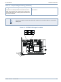
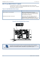
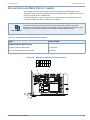
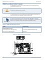
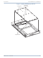
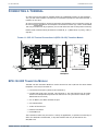
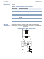
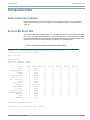
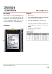
Document Number: 812628
Version: 1
Date: October 2003
SCP/DCP-122
3U COMPACTPCI
SINGLE BOARD COMPUTER
GETTING STARTED MANUAL
DY 4 Systems Inc.
333 Palladium Drive
Kanata, Ontario, Canada
K2V 1A6
(613) 599-9199
SCP/DCP-122 GETTING STARTED MANUAL
DY 4 SYSTEMS INC.
VERSION HISTORY
Version
By
Date
Description
1
JP
October 2003
New document release.
COPYRIGHT NOTICE
The information in this document is subject to change without notice and should not be
construed as a commitment by Dy 4 Systems Inc. While reasonable precautions have been
taken, Dy 4 Systems Inc. assumes no responsibility for any errors that may appear in this
document.
No part of this document may be copied or reproduced without the prior written consent of
Dy 4 Systems Inc.
The proprietary information contained in this document must not be disclosed to others for
any purpose, nor used for manufacturing purposes, without written permission of Dy 4
Systems Inc. The acceptance of this document will be construed as an acceptance of the
foregoing condition.
Copyright © 2003, Dy 4 Systems Inc. All rights reserved.
TRADEMARKS
Flash is a trademark of Seeq Technology.
All other brand and product names are trademarks or registered trademarks of their
respective owners.
II
812628 VERSION 1 OCTOBER 2003
DY 4 SYSTEMS INC.
TABLE OF CONTENTS
1. Product Overview ....................................................................................................... 1-1
Introducing the SCP/DCP-122 ................................................................................................ 1-1
Features List ..................................................................................................................1-2
PMC Expansion ............................................................................................................... 1-2
Physical Characteristics ......................................................................................................... 1-4
Weight Limits ................................................................................................................. 1-5
Dimensions .................................................................................................................... 1-5
Mating Connectors .......................................................................................................... 1-5
Electrical Characteristics ........................................................................................................ 1-6
Power Requirements........................................................................................................ 1-6
Voltage Requirements...................................................................................................... 1-6
Overview of Supplied Firmware .............................................................................................. 1-7
Foundation Firmware ....................................................................................................... 1-7
Board Support Packages, Drivers ...................................................................................... 1-7
2. Pre-Installation Tasks................................................................................................. 2-1
Introduction......................................................................................................................... 2-1
Unpacking the Card .............................................................................................................. 2-1
Configuring Jumpers ............................................................................................................. 2-2
Boot Flash Write Protect Jumper ....................................................................................... 2-4
Application Flash Write Protect Jumper............................................................................... 2-5
PABS Flash Write Protect Jumper ...................................................................................... 2-6
Boot From PABS Memory ................................................................................................. 2-7
Watchdog Timer Behaviour............................................................................................... 2-8
Execution Sequence Control Jumper .................................................................................. 2-9
Backup FPGA Boot PROM Jumper (Reserved) .................................................................... 2-10
3. Installing PMC Modules on the SCP/DCP-122.......................................................... 3-1
Before You Begin .................................................................................................................. 3-1
Installation Procedure ........................................................................................................... 3-2
Unpack and Configure the Card......................................................................................... 3-2
Install the PMC Module on the SCP/DCP-122....................................................................... 3-2
4. Hardware Installation.................................................................................................. 4-1
Introduction......................................................................................................................... 4-1
Inserting the Card in a Chassis ............................................................................................... 4-2
Before You Begin... ......................................................................................................... 4-2
About Card Insertion Force............................................................................................... 4-2
Choosing a Slot Location .................................................................................................. 4-2
Connecting a Terminal ..........................................................................................................4-3
BPK-122-000 Transition Module ........................................................................................ 4-3
Controlling the Boot Sequence ............................................................................................. 4-15
Foundation Firmware Used During Power-Up..................................................................... 4-15
Initiating the Power-Up Sequence ......................................................................................... 4-16
Power-Up..................................................................................................................... 4-16
Initial LED Activity......................................................................................................... 4-16
Displaying the Initial Screen Message.................................................................................... 4-16
Troubleshooting ................................................................................................................. 4-17
Verify Insertion in Chassis .............................................................................................. 4-17
Status LED Stays Red .................................................................................................... 4-17
Sign-on Message Garbled............................................................................................... 4-21
The Next Step .............................................................................................................. 4-21
812628 REVISION 1 OCTOBER 2003
III
SCP/DCP-122 GETTING STARTED MANUAL
IV
DY 4 SYSTEMS INC.
812628 REVISION 1 OCTOBER 2003
DY 4 SYSTEMS INC.
LIST OF FIGURES
Figure
Figure
Figure
Figure
Figure
Figure
Figure
Figure
Figure
Figure
Figure
Figure
Figure
Figure
Figure
Figure
Figure
Figure
Figure
1.1:
1.2:
1.3:
1.4:
2.1:
2.2:
2.3:
2.4:
2.5:
2.6:
2.7:
2.8:
3.1:
4.1:
4.2:
4.3:
4.4:
4.5:
4.6:
DCP-122 .............................................................................................................1-1
SCP/DCP-122 Functional Block Diagram .................................................................. 1-3
SCP-122 Component Side View .............................................................................. 1-4
SCP-122 Solder Side View ..................................................................................... 1-4
SCP/DCP-122 Jumper Locations ............................................................................. 2-3
Boot Flash Write Protect Jumper ............................................................................ 2-4
Application Flash Write Protect Jumper.................................................................... 2-5
PABS Flash Write Protect Jumper ........................................................................... 2-6
Boot From PABS Memory Jumper ........................................................................... 2-7
Watchdog Timer Power-up Jumper ......................................................................... 2-8
Execution Sequence Control Jumper ....................................................................... 2-9
FPGA Boot PROM Select ...................................................................................... 2-10
Installing a PMC Module on a DCP-122 .................................................................... 3-3
SCP-122 Terminal Connection via (BPK-122-000) Transition Module ........................... 4-3
Digital I/O via the Transition Module....................................................................... 4-5
EIA-422 Channel 3 and Channel 4 Header Pins......................................................... 4-7
Using the CBL-SBC-P0-000 with the Transition Module .............................................. 4-8
CBL-700-001 Used in Conjunction with BPK-122-000 ................................................ 4-9
Sample Diagnostics Results Table (DRT) ............................................................... 4-17
812628 VERSION 1 OCTOBER 2003
V
SCP/DCP-122 GETTING STARTED MANUAL
VI
DY 4 SYSTEMS INC.
812628 VERSION 1 OCTOBER 2003
DY 4 SYSTEMS INC.
LIST OF TABLES
Table
Table
Table
Table
Table
Table
Table
Table
Table
Table
Table
Table
Table
Table
Table
Table
Table
Table
Table
Table
Table
Table
Table
Table
1.1:
1.2:
1.3:
2.1:
2.2:
2.3:
2.4:
2.5:
2.6:
2.7:
2.8:
4.1:
4.2:
4.3:
4.4:
4.5:
4.6:
4.7:
4.8:
4.9:
4.10:
4.11:
4.12:
4.13:
Maximum CCA Mass ............................................................................................. 1-5
Dimensions of the SCP/DCP-122 ............................................................................ 1-5
SCP/DCP-122 Board Current Requirements.............................................................. 1-6
Jumper Settings Summary .................................................................................... 2-2
Boot Flash Write Protect Jumper ............................................................................ 2-4
Application Flash Write Protect Jumper.................................................................... 2-5
PABS Flash Write Protect Jumper ........................................................................... 2-6
Enable Booting from PABS Memory......................................................................... 2-7
Watchdog Timer Power-up Behaviour ..................................................................... 2-8
User Link Configuration......................................................................................... 2-9
Backup FPGA Boot PROM Select ........................................................................... 2-10
Serial Channel 1 RS-232 Connector (BPK-122-000 J3) Pinout..................................... 4-4
Serial Channel 2 RS-232 Connector (BPK-122-000 J6) Pinout..................................... 4-4
USB Connector (BPK-122-000 J4) Pinout................................................................. 4-4
Ethernet Connector (BPK-122-000 J5) Pinout........................................................... 4-5
DIO Header Pinout ............................................................................................... 4-6
EIA-422 Channel 3 Pinout ..................................................................................... 4-7
EIA-422 Channel 4 Pinout ..................................................................................... 4-7
Transition Module P0 Row A Signal Mapping .......................................................... 4-10
Transition Module P0 Row B Signal Mapping .......................................................... 4-11
Transition Module P0 Row C Signal Mapping .......................................................... 4-12
Transition Module P0 Row D Signal Mapping .......................................................... 4-13
Transition Module P0 Row E Signal Mapping........................................................... 4-14
Foundation Firmware Execution Sequence ............................................................. 4-15
812628 VERSION 1 OCTOBER 2003
VII
SCP/DCP-122 GETTING STARTED MANUAL
VIII
DY 4 SYSTEMS INC.
812628 VERSION 1 OCTOBER 2003
DY 4 SYSTEMS INC.
PREFACE
PURPOSE
This manual provides an overview of the features and functions of the SCP/DCP-122 Single
Board Computer and explains how to correctly install the card and verify its basic operation.
AUDIENCE
This manual is intended for the reader who has a technical understanding of hardware
engineering fundamentals, and a basic understanding of the CompactPCI architecture.
Cross Reference
More in-depth technical information about the SCP/DCP-122 hardware is provided in the
SCP/DCP-122 Hardware User’s Manual, document number 812629, which is included in the
documentation package.
DOCUMENTATION ROADMAP
The figure below will help you understand what documentation is available for the SCP/DCP122 and related products. These documents are delivered in Adobe Acrobat.pdf format on CDROM, or may be obtained via our TechNet web site at http://www.technet.dy4.com/.
SCP/DCP-122
Getting Started
Manual
812628
Contents:
- product overview
- hardware jumper configuration
- unpacking and installation
- cable hook-up and initial
system check-out
SCP/DCP-122
Hardware User's
Manual
812629
Contents:
- hardware functional description
- detailed connector pinout info.
- programming interface
description, including registers,
memory maps etc.
SCP/DCP-201
(PMC Carrier
Card)
User's Manual
811557
Contents:
- product overview
- installation requirements
- PMC module installation
- chassis installation
- connector pin assignments
SCP/DCP-122
Product Release
Notes
PMC Module
User's Manuals
8xxxxx
8xxxxx
Contents:
- information about the specific
hardware configuration of your
particular variant
Contents:
- provide hardware-related
information specific to PMC
modules that may be present
on either your SCP/DCP-122
or SCP/DCP-201.
SCP/DCP-122 Hardware Documentation
SCP/DCP-122
Foundation
Firmware
Release Notes
812xxx
Contents:
- details of the embedded
firmware on the SCP/DCP-122
- firmware updating instructions
- firmware release history
Foundation
Firmware User's
Manual
808006
Contents:
- comprehensive reference
manual for GPM, ES, CSS,
CLD, PBIT, etc.
SCP/DCP-122
Board Support
Package User's
Manual
812xxx
SCP/DCP-122
Board Support
Package
Release Notes
812xxx
(delivered on
BSP distribution
media)
(delivered on
BSP distribution
media)
Contents:
- provides BSP installation
instructions
- provides detailed BSP function
descriptions
Contents:
- summarizes the new features
and bug fixes contained in a
particular BSP release
PMC Module
Software User's
Manuals
8xxxxx
Contents:
- provide software driver-related
information specific to PMC
modules that may be present
on either your SCP/DCP-122
or SCP/DCP-201.
SCP/DCP-122 Software Documentation
812628 VERSION 1 OCTOBER 2003
IX
SCP/DCP-122 GETTING STARTED MANUAL
DY 4 SYSTEMS INC.
SCOPE OF THIS MANUAL
This manual contains the following chapters:
Chapter 1 - Product Overview. Provides general information about the features and
functions of the SCP/DCP-122.
Chapter 2 - Pre-Installation Tasks. Discusses tasks that must be performed prior to
installing the SCP/DCP-122 in a chassis. Provides information on jumper configurations,
cabling, and power requirements.
Chapter 3 - Installing PMC Modules on the SCP/DCP-122. Explains how to ensure that
thermal and mechanical requirements for PMC module mounting are met when mounting PMC
modules on the SCP/DCP-122.
Chapter 4 - Hardware Installation. Explains how to install the SCP/DCP-122 in a chassis
and verify that it is operating correctly.
CONVENTIONS USED IN THIS MANUAL
This document and the accompanying documents in the documentation package use various
icon conventions and abbreviations to make the documents clearer and easier to read. These
conventions cover typography for such elements as sample software code and keystrokes,
signal meanings, and graphical elements for important information such as warnings or
cautions.
Typographic
Conventions
Table 1 lists the typographical conventions used in documents contained in this document and
the associated documentation package.
TABLE 1: Typographical Conventions
Item
Convention
Example
Keystrokes
Keys are listed as they appear on most keyboards,
surrounded by < > marks. Combinations of keystrokes appear within a single set of < > brackets.
File names are set in italics.
Directory names show the full directory path. The last
directory in the path does not have a trailing slash
following it.
Prompts and other text appearing on monitors is set
in bold monospace type.
Firmware code, and any information you need to
type in response to a prompt, is set in monospace
type.
Type < Ctrl-Alt-C > to return to the previous menu.
Type < Esc > to exit.
File Names
Directory Names
Monitor Displays
Firmware Code
Signal
Conventions
Open the file named es.h.
Go to the c:\windows\temp\backup directory.
% mpp MC68040gnu >
% make -f Makefile.MC68040gnu
Table 2 shows symbols which can follow a signal name. For example, the octothorpe (#) is
used with a PCI signal name, such as TRDY#.
TABLE 2: Signal Conventions
Symbol
Description
[no symbol]
The signal is active HIGH (with no indication as to
which bus the signal is connected).
The signal is active LOW and is connected to the
PCI bus.
#
X
812628 VERSION 1 OCTOBER 2003
DY 4 SYSTEMS INC.
Abbreviations
Table 3 lists the abbreviations used to describe the size of a memory device or a range of
addresses.
TABLE 3: Abbreviations
Abbreviation
Convention
1 Kbyte
1 Mbyte
1 Gbyte
1,024 bytes
1,024 Kbytes
1,024 Mbytes
Memory
Addresses
Unless otherwise stated, all memory addresses are shown in hexadecimal notation.
Icons
The following icons are used throughout this document:
Cross Reference
Warning
Caution
Cross references to other documents are used when a subject being discussed is addressed
in depth by another, more authoritative document. Cross references are also used for
document chapters and sections.
The warning icon indicates procedures in the manual that, if not carried out, or if carried out
incorrectly, could cause physical injury, electrical damage to equipment, or a nonrecoverable corruption of data. Warnings include instructions for preventing such damage.
Please observe warning icons and read the accompanying text completely before carrying
out the procedure.
The caution icon indicates non-catastrophic incidents, complex practices, or procedures
which, if not observed, could result in damage to the hardware. Cautions include specific
instructions for avoiding or minimizing these incidents.
The note icon highlights exceptions and special information.
Note
Tips provide extra information on the subject matter. This could include hints about how to
use your current DY 4 card to its maximum potential.
Tip
812628 VERSION 1 OCTOBER 2003
XI
SCP/DCP-122 GETTING STARTED MANUAL
XII
DY 4 SYSTEMS INC.
812628 VERSION 1 OCTOBER 2003
1
PRODUCT OVERVIEW
INTRODUCING THE SCP/DCP-122
Designed for space constrained applications, the SCP/DCP-122 offers the greatest
processing power of any ruggedized 3U cPCI single board computer on the market today.
Based on the IBM 750FX processor, it runs at a clock speed of 800 MHz while executing an
impressive 1856 Dhrystone Millions of Instructions per Second (DMIPS). No other rugged
COTS 3U cPCI single board computer can match the raw processing power of the SCP/DCP122.
FIGURE 1.1: DCP-122
812628 VERSION 1 OCTOBER 2003
1-1
SCP/DCP-122 GETTING STARTED MANUAL
DY 4 SYSTEMS INC.
FEATURES LIST
•
Based on the IBM PowerPC 750FX processor
– 800+ MHz
– 1856+ DMIPS
– 100 MHz CPU bus speed
– 512 Kbyte of Internal L2 Cache running at core processor speed
•
cPCI Bus
– System controller and Peripheral controller
– 3.3V or 5V signalling supported
– 33 or 66MHz operation
•
PMC Expansion Site
– 64-bit, 33/66 MHz
– Support for 3.3V or +5V PMC’s
– Full 64-bit user I/O
•
Memory
– 128 Mbyte or 256 Mbyte of SDRAM with ECC at 100 MHz
– 64 Mbyte non-volatile Flash
– Flash for Permanent Alternate Boot Site (PABS)
– 32 Kbyte nonvolatile RAM
•
I/O
– 1 x 10/100BaseT Ethernet port
– 2 x RS-232 Serial port
– 2 x HDLC/SDLC-capable EIA 422 serial channels (2 asynchronous or 1
synchronous)
– 1 x USB
– 8 x general purpose DMA controllers
– Up to 16-bit Discrete I/O
PMC EXPANSION
To extend system flexibility and enhance system functionality through expansion, the
SCP/DCP-122 provides a full speed 64-bit 33/66 MHz PMC site directly on the basecard. A
complement of Dy 4 PMC's have been tested and qualified over temperature, shock and
vibration to ensure interoperability in harsh environments, including:
•
Trinity 2 - PMC-702 graphics controller
•
Trinity 1 - PMC-700 graphics controller
•
PMC-643 dual channel, conduction cooled Fibre Channel card
•
PMC-601 dual MIL-STD 1553 interface
Expansion can further be enhanced by combining the SCP/DCP-122 with Dy 4's conduction
cooled cPCI PMC carrier card, the SCP/DCP-201.
1-2
812628 VERSION 1 OCTOBER 2003
DY 4 SYSTEMS INC.
PRODUCT OVERVIEW
Figure 1.2 illustrates the architecture and major components of the SCP/DCP-122.
FIGURE 1.2: SCP/DCP-122 Functional Block Diagram
BP_3.3V
IBM750FX
512K L2 Cache
800MHz
Power
Conversion
DH
DL
Adr
Clocks
Ctrl
40
25
66
6
100
MHz MHz MHz MHz MHz
[31:0]
1.8V
2.5V
BP_5V
[31:0]
1.4V
Power
Sequencer
[31:0]
BP_5V
5V
BP_3.3V
3.3V
BP_VIO
VIO
CPU I/F
32/64 bit
33/66 MHz
5/3.3 Volt
32 bit
33/66 MHz
5/3.3 Volt
J1
Conn.
Muxed
I/O
Pins
10/100
transceiver
Ethernet
I/F
Transformer
Serial
I/F
SDRAM
I/F
CPU-PCI
Bridge
DISCO I
MPSC I/F
Non-Muxed I/O
Pins
PCI 1
I/F
termination
PMC
Conn.
PN4
Ctrl
PCI 0
I/F
termination
SDRAM + ECC
128/256MB
4 x 16M x 16
[12:0]
Adr
[63:0]
Data
Temp
Sensor
I2C I/F
MPP
I/F
Device I/F
Device Bus AD[31:0] & BADDR[2:0]
AD[24:3]
PMC
Conn.
PN1,2,3
10/100BASE-TX ETHERNET
SEEPROM
J2 Conn.
FPGA
422
Xceivers
ISP Prom
Buffer
Latch
OTP Prom
Device AD [27:4] & Device BADDR[2:0]
Peripheral Bus [7:0]
15:0
DUART
NVRAM/
RTC
PABS
USB Host
Controller
31:0
DEV_DATA [31:0]
DIO[15:0]
31:0
I/O Mux
Scheme
Flash
Bank 0
32MBytes
Flash
Bank 1
32MBytes
RS232
transceiver
RS-232 CH1
Cross Reference
RS-232
CH2
Production Test
JTAG I/F
Debug Port
COPS I/F
Please refer to Chapter 1 of the SCP/DCP-122 Hardware User’s Manual, document number
812629, for a detailed description of each of the functional blocks in the above diagram.
812628 VERSION 1 OCTOBER 2003
1-3
SCP/DCP-122 GETTING STARTED MANUAL
DY 4 SYSTEMS INC.
PHYSICAL CHARACTERISTICS
The following figures will help familiarize you with the location of the major components and
connnectors of the SCP/DCP-122. Although the SCP-122 is used for illustration purposes, the
board layout for the DCP version product is identical.
FIGURE 1.3: SCP-122 Component Side View
IBM750FX
SDRAM
J2
PN1
PN2
PN3
PN4
GT-64260
Discovery
J1
SDRAM
FIGURE 1.4: SCP-122 Solder Side View
Flash
Flash
Flash
USB
SDRAM
SDRAM
SDRAM
Flash
Flash
(PABS)
1-4
Eth/Phy
812628 VERSION 1 OCTOBER 2003
DY 4 SYSTEMS INC.
PRODUCT OVERVIEW
The SCP/DCP-122 board has the following physical characteristics:
WEIGHT LIMITS
The mass of the SCP/DCP-122 board does not exceed the values specified in Table 1.1.
TABLE 1.1: Maximum CCA Mass
Card Type
Weight (grams)
DPMC
150
SPMC
200
DIMENSIONS
The SCP/DCP-122 is built on a CompactPCI-compatible single-height (3U) PWB. Table 1.2
lists the dimensions of the SCP/DCP-122.
TABLE 1.2: Dimensions of the SCP/DCP-122
Parameter
Dimensions
Height
100 mm
Depth
160 mm
MATING CONNECTORS
The locations of the connectors on the SCP/DCP-122 are shown in Figure 1.3.
Backplane
Connectors
The SCP/DCP-122 incorporates J1 and J2 connectors as specified in the PICMG compact PCI
specification 2.0, Revision 3.0.
PMC Connectors
In order to support the mounting of a single PCI Mezzanine Card (PMC) in accordance with
the IEEE 1386-2001 standard, the SCP/DCP-122 includes the Pn1, Pn2, Pn3 and Pn4
connectors as specified in the standard.
812628 VERSION 1 OCTOBER 2003
1-5
SCP/DCP-122 GETTING STARTED MANUAL
DY 4 SYSTEMS INC.
ELECTRICAL CHARACTERISTICS
POWER REQUIREMENTS
The SCP/DCP-122 maximum and typical power requirements are listed in Table 1.3.
TABLE 1.3: SCP/DCP-122 Board Current Requirements
Voltage
Maximum Current
Typical Current
+3.3V (+5%, -3%)
1.1 A
0.9 A
+5V (+5%, -3%)
2.2 A
1.8 A
+12V ± 0.6V (± 5%)
0A
Not used by the base card, only routed to the PMC
sites.
-12V ± 0.6V (± 5%)
0A
Not used by the base card, only routed to the PMC
sites.
The power dissipation of the SCP/DCP-122 ranges between 12 watts (typical) and 15 watts
(maximum), as measured on a small sampling of product over a limited operating
temperature range, with no PMC module installed.
VOLTAGE REQUIREMENTS
The SCP/DCP-122 expects the following voltages to be available from the compact PCI
backplane, as specified in the PICMG specification: 5V, 3.3V, +VIO, +12V, and -12V.
1-6
812628 VERSION 1 OCTOBER 2003
DY 4 SYSTEMS INC.
PRODUCT OVERVIEW
OVERVIEW OF SUPPLIED FIRMWARE
FOUNDATION FIRMWARE
The SCP/DCP-122 is programmed with the following Foundation Firmware (FFW) modules:
Cross Reference
•
General Purpose Monitor (GPM): provides comprehensive monitoring and debug functions, which can be accessed from a terminal connected to the SCP/DCP-122 serial
channel 1 interface
•
Card Level Diagnostics (CLD): provides diagnostic routines which work with your card’s
Built-In-Test functions
•
Card Support Services (CSS): provides a software interface to your card’s hardware
•
Execution Sequencer (ES): controls the execution sequence of software during a card’s
boot-up
•
Non-Volatile Memory Programmer (NVMP): provides for in-circuit programming of
Flash memory.
Refer to the FF/W Software User Manual (document number 808006) and the FF/W
Programmer’s Reference (document number 812587) (included in the documentation
package) for additional information.
See also the Dy 4 Troubleshooting Wizard, which is available for your convenience at
http://www.technet.dy4.com/wizard/index.htm (or simply click the FAQ link on the TechNet
home page).
BOARD SUPPORT PACKAGES, DRIVERS
Support is provided for the VxWorks operating system. The VxWorks boot loader is preloaded on the SCP/DCP-122 hardware. Refer to the BSP Release Notes and the BSP Software
User’s Manual (delivered on the BSP s/w CD-ROM) for additional information.
812628 VERSION 1 OCTOBER 2003
1-7
SCP/DCP-122 GETTING STARTED MANUAL
1-8
DY 4 SYSTEMS INC.
812628 VERSION 1 OCTOBER 2003
2
PRE-INSTALLATION TASKS
INTRODUCTION
This chapter explains how to configure the SCP/DCP-122 before it is installed in a
CompactPCI chassis. Specifically, this chapter provides the following information:
•
unpacking the card
•
modifying the SCP/DCP-122 jumper settings
•
checking cable and power requirements.
UNPACKING THE CARD
Warning
This card uses components that are sensitive to electrostatic discharges. It must be kept in
its conductive package until just before the installation begins. Remove the card from its
protective package only at a grounded workstation while wearing an approved grounding
wrist strap. Avoid touching any metal contacts on the card; static discharge can damage
integrated circuits. To avoid damage to the card or to avoid any personal injury, remove the
power from the chassis prior to removing or installing cards.
To unpack the card from its protective package, follow these steps:
1. Unpack the card from the shipping carton in a suitable work area. If the shipping carton appears to be damaged, request that an agent of the shipper or carrier be present
during unpacking and inspection.
2. Find the packing list. Verify that all the items on the list are present.
3. Save the packing material for storing or reshipping the card.
812628 VERSION 1 OCTOBER 2003
2-1
SPMC/DPMC-122 GETTING STARTED MANUAL
DY 4 SYSTEMS INC.
CONFIGURING JUMPERS
Cross Reference
Depending on your application, it may be necessary to modify the default jumper settings
on your SCP/DCP-122. For information about your card’s default configuration, refer to the
Product Release Note.
Table 2.1 summarizes the user-configurable jumper settings. In-depth descriptions of these
settings are provided in subsequent pages.
Factory configurations are performed via the installation/removal of configuration resistors.
Please contact the factory if you require information about factory configured options. Under
normal circumstances, you should not need to alter any of the factory-configured options.
TABLE 2.1: Jumper Settings Summary
Option
Jumper Setting
Flash Boot Write Protect Enable/Disable:
Disable Flash Boot Write Protect.
Connect E1-E2
Enable Flash Boot Write Protect.
Open E1-E2
Flash Application Bank Write Protect Enable/Disable:
Disable Flash Application Bank Write Protect.
Connect E3-E4
Enable Flash Application Bank Write Protect.
Open E3-E4
Enable Writes to Permanent Alternate Boot Site (PABS)
Memory:
Disable Permanent Alternate Boot Bank Write Protect.
Connect E5-E6 (caution: for factory use only)
Enable Permanent Alternate Boot Bank Write Protect.
Open E5-E6 (normal configuration)
Boot from the Permanent Alternate Boot Site (PABS):
Boot from 8-bit PABS site.
Connect E7-E8
Boot from the main Flash memory.
Open E7-E8
Configuring Watchdog Timer Behaviour:
Watchdog timer generates an interrupt on timeout.
Connect E9-E10
Watchdog timer generates a reset on timeout.
Open E9-E10
Changing the Execution Sequence during Card Boot Up:
(see “Controlling the Boot Sequence” on page 4-15 for more
information)
Connect E11-E12 to connect User Link/Software Switch (SW0)
signal to ground.
Open E11-E12 to pull up User Link/Software Switch (SW0)
2-2
812628 VERSION 1 OCTOBER 2003
DY 4 SYSTEMS INC.
PRE-INSTALLATION TASKS
TABLE 2.1: Jumper Settings Summary (Continued)
Configure FPGA from Back-up PROM (Reserved):
A provision for a Back-up PROM for the FPGA exists in the
design of the SCP/DCP-122, however it has not been implemented at the present time, meaning the jumper at E13-E14
must not be connected.
Open E13-E14
All other E jumper locations not specifically mentioned in the above table are reserved for
factory use.
Note
812628 VERSION 1 OCTOBER 2003
E13 E14
E11 E12
E9 E10
E7 E8
E5 E6
E3 E4
E1 E2
FIGURE 2.1: SCP/DCP-122 Jumper Locations
2-3
SPMC/DPMC-122 GETTING STARTED MANUAL
DY 4 SYSTEMS INC.
BOOT FLASH WRITE PROTECT JUMPER
The SCP/DCP-122 provides a jumper to allow programming of the main boot Flash.
Normally, the E1-2 jumper is not installed and the boot Flash is write-protected. To program
the boot Flash, install the E1-E2 jumper.
TABLE 2.2: Boot Flash Write Protect Jumper
Option
Jumper Setting
Main Boot Flash is write-protected.
Open E1-E2 (normal mode). In this mode, the
WP_BOOT_BIT (described further in “E2PROM General
Control Register” in Chapter 3 of the SCP/DCP-122 Hardware User’s Manual) is Read Only.
Disable Main Boot Flash write-protect.
Connect E1-E2. In this mode, application software can
change the WP_BOOT_BIT to write protect or not
(described further in “E2PROM General Control Register” in
Chapter 3 of the SCP/DCP-122 Hardware User’s Manual).
Cross Reference
2-4
E13 E14
E11 E12
E9 E10
E7 E8
E5 E6
E3 E4
E1 E2
FIGURE 2.2: Boot Flash Write Protect Jumper
The state of the E1-E2 jumper is shown in the WR_PROT_BOOT_JMP bit in the FPGA
Miscellaneous Signal Status Register. See Chapter 3 of the SCP/DCP-122 Hardware User’s
Manual for more information about the Miscellaneous Signal Status Register.
812628 VERSION 1 OCTOBER 2003
DY 4 SYSTEMS INC.
PRE-INSTALLATION TASKS
APPLICATION FLASH WRITE PROTECT JUMPER
The SCP/DCP-122 provides a jumper to allow programming of the application Flash.
“Application Flash” means all Flash areas except the PABS Flash. The application Flash is in
the range 0xFC00 0000 to 0xFDFF FFFF.
For normal operation, remove jumper E3-E4 to write-protect the application Flash. To
program the application Flash, install the E3-E4 jumper.
Cross Reference
The state of the E3-E4 jumper is shown in the WR_PROT_APP_JMP bit in the FPGA
Miscellaneous Signal Status Register. See Chapter 3 of the SCP/DCP-122 Hardware User’s
Manual for more information about the Miscellaneous Signal Status Register.
TABLE 2.3: Application Flash Write Protect Jumper
Option
Jumper Setting
Application Flash Write Protect:
Program application Flash bank
Connect E3-E4
Do not program application Flash bank
Open E3-E4
812628 VERSION 1 OCTOBER 2003
E13 E14
E11 E12
E9 E10
E7 E8
E5 E6
E3 E4
E1 E2
FIGURE 2.3: Application Flash Write Protect Jumper
2-5
SPMC/DPMC-122 GETTING STARTED MANUAL
DY 4 SYSTEMS INC.
PABS FLASH WRITE PROTECT JUMPER
The SCP/DCP-122 provides a jumper to allow programming of the PABS (Permanent
Alternate Boot Site) Flash area.
This jumper is intended for factory use only.
Caution
For normal operation, remove the jumper E5-E6 so that the PABS is write-protected. To
enable programming of the PABS Flash, install the E5-E6 jumper.
The state of the E5-E6 jumper is shown in the WR_PROT_PABS_JMP bit in the FPGA
Miscellaneous Signal Status Register. See Chapter 3 of the SCP/DCP-122 Hardware User’s
Manual for more information about the Miscellaneous Signal Status Register.
Cross Reference
TABLE 2.4: PABS Flash Write Protect Jumper
Option
Jumper Setting
PABS Flash Write Protect:
Enable programming of PABS Flash bank
Connect E5-E6 (caution: for factory use only)
Write protect the PABS Flash bank
Open E5-E6
2-6
E13 E14
E11 E12
E9 E10
E7 E8
E5 E6
E3 E4
E1 E2
FIGURE 2.4: PABS Flash Write Protect Jumper
812628 VERSION 1 OCTOBER 2003
DY 4 SYSTEMS INC.
PRE-INSTALLATION TASKS
BOOT FROM PABS MEMORY
The SCP/DCP-122 includes a 32-bit Flash bank and a PABS site. You may boot the SCP/DCP122 from either of these sources. Normally, the SCP/DCP-122 boots from 32-bit Flash.
However, if the Foundation Firmware in the 64-bit Flash is corrupted, you may boot from the
PABS site. Once you have booted the card you may use FFWUPD, FlashProg, or NVMP to
reprogram the 32-bit Flash. You can then power off the card and remove the jumper to allow
local booting. Use the jumper settings described in Table 2.5 to select the bank used for
booting. The location of the jumper is shown in Figure 2.5 below.
TABLE 2.5: Enable Booting from PABS Memory
Option
Jumper Setting
Boot from 8-bit PABS site.
Connect E7-E8
Boot from 32-bit main Flash
Open E7-E8
E13 E14
E11 E12
E9 E10
E5 E6
E7 E8
E3 E4
E1 E2
FIGURE 2.5: Boot From PABS Memory Jumper
The functionality described above is optionally available on the SCP/DCP-122 J2 connector,
using the ALT_BOOT- signal in place of DIO7 (J2-C11).
Note
812628 VERSION 1 OCTOBER 2003
2-7
SPMC/DPMC-122 GETTING STARTED MANUAL
DY 4 SYSTEMS INC.
WATCHDOG TIMER BEHAVIOUR
The SCP/DCP-122 offers the capability of enabling the watchdog timer immediately following
reset without the need for software programming or initialization. This mode of operation is
selected by leaving E9-E10 open. The watchdog timer will generate a card reset if left to
expire.
With the E9-E10 jumper installed, the watchdog timer is disabled following power-up reset;
however, it can be enabled by application software.
TABLE 2.6: Watchdog Timer Power-up Behaviour
Option
Jumper Setting
Watchdog timer is disabled following power-up:
(generates interrupt on timeout).
Connect E9-E10
Watchdog timer is enabled following power-up:
(generates a card reset on timeout).
Open E9-E10
2-8
E13 E14
E11 E12
E7 E8
E9 E10
E5 E6
E3 E4
E1 E2
FIGURE 2.6: Watchdog Timer Power-up Jumper
812628 VERSION 1 OCTOBER 2003
DY 4 SYSTEMS INC.
PRE-INSTALLATION TASKS
EXECUTION SEQUENCE CONTROL JUMPER
The SCP/DCP-122 has a software-readable jumper located at E11-E12. This jumper, referred
to as the User Link or Software Switch, is used to control the power-up sequence for the
Foundation Firmware and applications.
The on-board Foundation Firmware checks the state (connected or open) of the User Link on
power-up and uses this along with the serial channel 1 DSR input to select one of four
possible execution sequences. See “Initiating the Power-Up Sequence” on page 4-16 for
more information.
For information on the code executed, refer to the SCP/DCP-122 Programmer’s Reference
Manual.
Factory configurations are performed via the installation/removal of configuration resistors.
Please contact the factory if you require information about factory configured options. Under
normal circumstances, you should not need to alter any of the factory-configured options.
TABLE 2.7: User Link Configuration
Option
Jumper Setting
Execution Sequencer Control:
(sets the PCI Control and Status Register bit SW0 = 0).
Connect E11-E12
(sets the PCI Control and Status Register bit SW0 = 1).
Open E11-E12
812628 VERSION 1 OCTOBER 2003
E11 E12
E13 E14
E9 E10
E7 E8
E5 E6
E3 E4
E1 E2
FIGURE 2.7: Execution Sequence Control Jumper
2-9
SPMC/DPMC-122 GETTING STARTED MANUAL
DY 4 SYSTEMS INC.
BACKUP FPGA BOOT PROM JUMPER (RESERVED)
The SCP/DCP-122 has a provision for a jumper to select a backup FPGA boot PROM, however
no backup FPGA boot PROM is implemented in the current design of the SCP/DCP-122.
Therefore the jumper E13-E14 must be removed in order to use the normal FPGA boot
PROM.
TABLE 2.8: Backup FPGA Boot PROM Select
Option
Jumper Setting
Backup FPGA Boot PROM (Reserved):
A provision for a Back-up PROM for the FPGA exists in the
design of the SCP/DCP-122, however it has not been implemented at the present time, meaning the jumper at E13-E14 must
not be connected.
Open E13-E14
2-10
E13 E14
E11 E12
E7 E8
E9 E10
E5 E6
E3 E4
E1 E2
FIGURE 2.8: FPGA Boot PROM Select
812628 VERSION 1 OCTOBER 2003
3
INSTALLING PMC MODULES ON THE
SCP/DCP-122
BEFORE YOU BEGIN
Warning
PMC modules include components that are sensitive to electrostatic discharges.
Keep your PMC module in its conductive package until just before the installation
begins. Remove the card from its protective package only at a grounded
workstation while wearing an approved grounding wrist strap. Avoid touching any
metal contacts on the card; static discharge can damage integrated circuits. To
avoid damage to the card or to avoid any personal injury, remove the power from
the chassis prior to removing or installing cards.
812628 VERSION 1 OCTOBER 2003
3-1
SCP/DCP-122 GETTING STARTED MANUAL
DY 4 SYSTEMS INC.
INSTALLATION PROCEDURE
Follow the instructions in this chapter to install it on the carrier card.
UNPACK AND CONFIGURE THE CARD
1. Unpack the PMC module from the shipping carton in a suitable work area. If the shipping carton appears to be damaged, request that an agent of the shipper or carrier be
present during packing and inspection.
2. Find the packing list. Verify that all items on the list are present.
3. Save the packing material for storing or reshipping the card.
Before installing the PMC module on the SCP/DCP-122, ensure that you complete all
pre-installation tasks described in the associated PMC user documentation.
INSTALL THE PMC MODULE ON THE SCP/DCP-122
Install your PMC module on the SCP/DCP-122 using the appropriate mounting kit available
from Dy 4 Systems. This kit contains all the screws and additional hardware you need to
ensure that the PMC module is firmly installed on your SCP/DCP-122.
Installing a PMC
Module on a
DCP-122
Figure 3.1 on page 3-3 shows a PMC module in position over a DCP-122.
If the PMC module you are installing on the DCP-122 is not a Dy 4 product, make sure the
module has a compatible thermal frame.
Note
Thermal gaskets in the PMC mounting kit ensure a good thermal connection between the
frame of the PMC module and the carrier card. These gaskets are white strips of thermal
material with holes to match the holes in the primary and secondary thermal interfaces (five
holes on the primary interface, and three holes on the secondary). Remove the backing from
the thermal gaskets and affix them to the thermal frame of your PMC module.
Your mounting kit may include thermal pads of a thicker material to conduct heat away from
some components through the thermal frame on the carrier card. Remove the backing from
the pads and affix them to the appropriate components.
The kits also contain at least eighteen 2 mm screws with washers and two 2.5 mm screws
to fasten the PMC module to the frame. The two 2.5 mm screws fasten the SCP/DCP-122 to
the two integral standoffs on the carrier card frame (as indicated in Figure 3.1).
Alternatively, if the carrier card frame does not include integral standoffs, use the individual
standoffs included in the mounting kit. The 2 mm screws and washers affix the card by the
primary and secondary thermal interfaces.
Torque the PMC mounting screws at exactly 4 lb-in, as indicated on the basecard generic
drawing supplied on your Dy 4 basecard Technical Documentation CD-ROM.
Note
3-2
Dy 4 Systems recommends using a thread locking compound, such as Loctite 222MS
Threadlocker (Dy 4 part number 163220) to prevent the screws from becoming loose.
812628 VERSION 1 OCTOBER 2003
DY 4 SYSTEMS INC.
INSTALLING PMC MODULES ON THE SCP/DCP-122
FIGURE 3.1: Installing a PMC Module on a DCP-122
2.5 mm screws
2 mm screws
w/washers (typ.)
Integral Standoffs
812628 VERSION 1 OCTOBER 2003
3-3
SCP/DCP-122 GETTING STARTED MANUAL
3-4
DY 4 SYSTEMS INC.
812628 VERSION 1 OCTOBER 2003
4
HARDWARE INSTALLATION
INTRODUCTION
This chapter explains how to install the SCP/DCP-122 in a CompactPCI chassis. Specifically
this chapter describes the following procedures:
•
inserting the card into a chassis
•
connecting a terminal to the card via a serial communications cable
•
connecting other devices to the card via the BPK-122-000 Transition Module
•
turning on the power and confirming that the Power-up Built-In Test (PBIT) has completed successfully
•
displaying the initial screen message and establishing the card’s PCI base address
•
troubleshooting installation problems.
812628 VERSION 1 OCTOBER 2003
4-1
SCP/DCP-122 GETTING STARTED MANUAL
DY 4 SYSTEMS INC.
INSERTING THE CARD IN A CHASSIS
BEFORE YOU BEGIN...
Warning
This card uses components that are sensitive to electrostatic discharges. It must be kept in
its conductive package until just before the installation begins. Remove the card from its
protective package only at a grounded workstation while wearing an approved grounding
wrist strap. Avoid touching any metal contacts on the card; static discharge can damage
integrated circuits.
Turn the power off before inserting or removing cards from the chassis. Failure to do so
could damage the card circuitry or cause personal injury.
ABOUT CARD INSERTION FORCE
The SCP/DCP-122 employs 110-pin connectors for the J1 and J2 interfaces. Proper mating
of these connectors with the CompactPCI backplane requires a significant amount of
insertion force. Use extra care when aligning and inserting your SCP/DCP-122 into your
chassis to ensure that a secure mechanical and electrical connection is made between the
card and the backplane mating connectors.
CHOOSING A SLOT LOCATION
If you want your SCP/DCP-122 to function as the system controller, insert your SCP/DCP122 in the system slot. The system slot is typically the leftmost or rightmost slot on the
backplane and is denoted by a “∆" symbol.
Either end slot on the backplane may be configured as the System Slot. Refer to the chassis
vendor’s documentation to determine which slot is the System Slot.
Note
The system controller provides the following to the CompactPCI bus:
•
arbitration
•
clocks
•
terminations
•
system reset
•
PCI configuration
If the SCP/DCP-122 is inserted into any of the peripheral slots, marked with a circle, it
functions as a peripheral card. A peripheral card requires a system controller to provide the
above functions.
4-2
812628 VERSION 1 OCTOBER 2003
DY 4 SYSTEMS INC.
HARDWARE INSTALLATION
CONNECTING A TERMINAL
In order to access the features available within the embedded firmware on the SCP/DCP122, you will need to attach a terminal or PC-emulated equivalent to the Serial Channel 1
interface on the card.
As seen in Figure 4.1 below, connect a terminal to the SCP/DCP-122 J2 connector via the J3
RS-232 connector provided on the SCP/DCP-122 transition module (Dy 4 order number BPK122-000) available from Dy 4 Systems (for use with either the SCP or DCP product versions).
Default serial communication parameters are 9600 N, 8, 1 (9600 baud, no parity, 8 bits, 1
stop bit).
FIGURE 4.1: SCP-122 Terminal Connection via (BPK-122-000) Transition Module
DIO
J2
CPCI
P0
Cable
I/F
J4
(USB)
RS-422 Ch3
and Ch 4
J5 Eth
Ch1
J3
RS-232
Ch2
J6
RS-232
Reset (E36, E37)
SCP-122
Transition Module
Chassis
Backplane
BPK-122-000 TRANSITION MODULE
The BPK-122-000 Transition Module is used to access the user's I/O from the CPCI chassis
backplane. The 122 I/O consists of:
•
two RS-232 serial ports (channel 1and channel 2)
•
two EIA-422 serial ports (channel 3 and channel 4). The 422 channels can be configured as two independent asynchronous channels or one synchronous channel (Ch4
data becomes CH3 clock)
•
one 10 Base-T/100 Base-TX Ethernet port
•
one USB interface
•
16 bits of discrete I/O
•
External card Reset
•
64-bit PMC I/O
The transition module may be used in a variety of applications, to optimize connectivity to
either the SCP/DCP-122 basecard, or any PMC module that may be installed on the
SCP/DCP-122.
812628 VERSION 1 OCTOBER 2003
4-3
SCP/DCP-122 GETTING STARTED MANUAL
BPK-122-000
Serial Channel 1
EIA-232 Interface
BPK-122-000
Serial Channel 2
EIA-232 Interface
BPK-122-000 USB
Interface
DY 4 SYSTEMS INC.
Table 4.1 summarizes the pinout information for the BPK-122-000 J3 (RJ-12) connector.
TABLE 4.1: Serial Channel 1 RS-232 Connector (BPK-122-000 J3) Pinout
J3 Pin Number
SCP/DCP-122 Signal Name
1
No Connect
2
No Connect
3
RX
4
TX
5
DSR
6
GND
Table 4.2 summarizes the pinout information for the BPK-122-000 J6 (RJ-12) connector.
TABLE 4.2: Serial Channel 2 RS-232 Connector (BPK-122-000 J6) Pinout
J6 Pin Number
SCP/DCP-122 Signal Name
1
No Connect
2
No Connect
3
RX
4
TX
5
No Connect
6
GND
Table 4.4 summarizes the pinout information for the BPK-122-000 J4 connector.
TABLE 4.3: USB Connector (BPK-122-000 J4) Pinout
4-4
J4 Pin Number
SCP/DCP-122 Signal Name
1
USB_VCC
2
USBD-
3
USBD+
4
GND
812628 VERSION 1 OCTOBER 2003
DY 4 SYSTEMS INC.
BPK-122-000
Ethernet Interface
HARDWARE INSTALLATION
Table 4.4 summarizes the pinout information for the BPK-122-000 J5 (RJ45) connector.
TABLE 4.4: Ethernet Connector (BPK-122-000 J5) Pinout
BPK-122-000
Transition Module
DIO Header
J5 Pin Number
SCP/DCP-122 Signal Name
1
ENET_TX+
2
ENET_TX-
3
ENET_RX+
4
NC
5
NC
6
ENET_RX-
7
NC
8
NC
The SCP/DCP-122 Digital I/O (DIO) signals are also available via header pins on the
transition module, as shown below in Figure 4.2. The center column of pins are GND signals.
FIGURE 4.2: Digital I/O via the Transition Module
DIO
DIO1
DIO8
DIO7
DIO15
DIO
J2
CPCI
P0
Cable
I/F
J4
(USB)
RS-422 Ch 3
and Ch 4
J5 Eth
Ch 1
J3
RS-232
Ch 2
J6
RS-232
Reset (E36, E37)
812628 VERSION 1 OCTOBER 2003
4-5
SCP/DCP-122 GETTING STARTED MANUAL
DY 4 SYSTEMS INC.
TABLE 4.5: DIO Header Pinout
DIO Pin
Number
Signal Name
DIO Pin
Number
Signal Name
DIO Pin
Number
Signal Name
E1
DIO0/RTC Standby
E9
GND
E17
DIO8
E2
DIO1
E10
GND
E18
DIO9
E3
DIO2
E11
GND
E19
DIO10
E4
DIO3
E12
GND
E20
DIO11
E5
DIO4
E13
GND
E21
DIO12
E6
DIO5
E14
GND
E22
DIO13
E7
DIO6
E15
GND
E23
DIO14
E8
DIO7/ALTBOOT
E16
GND
E24
DIO15
4-6
812628 VERSION 1 OCTOBER 2003
DY 4 SYSTEMS INC.
BPK-122-000
Transition Module
Channel 3 and 4
Header Pins
HARDWARE INSTALLATION
Figure 4.3 shows the location and orientation of the header pins on the transition module
associated with the Channel 3 and Channel 4 EIA-422 interfaces available from the
SCP/DCP-122.
FIGURE 4.3: EIA-422 Channel 3 and Channel 4 Header Pins
P0
Cable
I/F
J4
(USB)
RS-422 Ch 3
and Ch 4
J5 Eth
Ch 1
J3
RS-232
Ch 2
J6
RS-232
CHANNEL 3
J2
CPCI
TX+
TX+
TX-
TX-
RX-
RX-
RX+
RX+
GND
GND
CHANNEL 4
DIO
Reset (E36, E37)
TABLE 4.6: EIA-422 Channel 3 Pinout
Pin Number
SCP/DCP-122 Signal Name
E25
422_CH3_TX+
E26
422_CH3_TX-
E27
422_CH3_RX-
E28
422_CH3_RX+
E29
GND
Differential I/O Pair
Diff I/O Out 0
Diff I/O In 0
TABLE 4.7: EIA-422 Channel 4 Pinout
Pin Number
SCP/DCP-122 Signal Name
E30
422_CH4_TX+ / CH3_TXClock+
E31
422_CH4_TX- / CH3_TXClock-
E32
422_CH4_RX- / CH3_RXClock-
E33
422_CH4_RX+ / CH3_RXClock+
E34
GND
812628 VERSION 1 OCTOBER 2003
Differential I/O Pair
Diff I/O Out 1
Diff I/O In 1
4-7
SCP/DCP-122 GETTING STARTED MANUAL
Basecard I/O Mode
DY 4 SYSTEMS INC.
The default configuration assumes no PMC module is present on the SCP/DCP-122, allowing
the full range of basecard I/O to be distributed via the transition module. This includes the
following interfaces:
•
Optional basecard I/O allows for DIO7 to be replaced with ALT_BOOT-, and/or DIO0 to
be replaced by RTC standby power.
•
RS-232 is available on J3 and J6
•
Ethernet is available on J5
•
USB is available on J4
•
DIO (0) to DIO (15) available on header block
•
EIA-422 Channel 3 and 4 available on pin headers
•
Card Reset is routed to E36 and E37
Individual standard cables are required for RS-232, Ethernet and USB ports.
PMC-601 Support
If a PMC-601 is present on the SCP/DCP-122, the transition board provides access to the
PMC-601 signals in conjunction with the Dy 4’s standard SBC P0 cable (CBL-SBC-P0-000).
See Figure 4.4 below for more information.
This option supports the following combination of interfaces:
•
two RS-232 ports available on Transition Module J3 and J6 connectors.
•
64-bit PMC I/O available on the 78-Way connector via the P0 cable (into which the
PMC-601 cable assembly (#901321-000) may be connected to further break out the
MIL-STD-1553 signals)
•
Ethernet is available on J5 and it is also accessible via the P0 cable.
•
USB is not available (multiplexed with PMC I/O). The USB power signal (USBVBUS) is
isolated from the USB connectors (0 ohm resistor not populated)
•
Discrete I/O's are not available (multiplexed with PMC I/O)
•
one asynchronous EIA-422 serial port (CH3) accessible via on board pin headers. EIA422 channel 4 is not available (multiplexed with PMC I/O).
•
Card Reset is available on E36 and E37 and P0 cable
FIGURE 4.4: Using the CBL-SBC-P0-000 with the Transition Module
approx. 19" (50 cm)
J1: PMC I/O
via 78 pin HDP-22 Receptacle
P1
J2: Ethernet 10BASE-T or
100BASE-TX via RJ45S
DIO
J2
CPCI
P0
Cable
I/F
J4
(USB)
RS-422 Ch3
and Ch 4
J5 Eth
Ch1
J3
RS-232
Ch 2
J6
RS-232
J3: Discrete Digital I/O
via DB25
J4: USB
Reset (E36, E37)
Pushbutton
Reset
4-8
812628 VERSION 1 OCTOBER 2003
DY 4 SYSTEMS INC.
PMC-700 Support
HARDWARE INSTALLATION
If a PMC-700 is present on the SCP/DCP-122, the transition board provides access to the
PMC-700 signals in conjunction with the Dy 4’s standard PMC-700 P0 cable (CBL-700-001).
•
one RS-232 port available on BPK-122-000 J3 and P0 cable. 0 Ohm resistor is used to
route RS-232 to the 700 P0 cable. The 700 RS-232 signals share the same P0 pins with
DIO 13, DIO 14 and DIO 15. When RS-232 is routed to these pins, the user still have
access to all 16 DIO via the on board pin headers.
•
one 10 Base-T/100 Base-TX Ethernet Port available on J3 native connector and P0
cable.
•
one USB port available only on J4 native USB connector
•
12 bits of parallel I/O available via the P0 cable (but all 16 DIO are accessible via the
on board pin headers).
•
four pairs of TMDS signals accessible via the DVI connector on the P0 cable.
•
one VGA interface
Figure 4.5 below illustrates this in further detail:
FIGURE 4.5: CBL-700-001 Used in Conjunction with BPK-122-000
approx. 19" (50 cm)
DIO
J2
CPCI
P0
Cable
I/F
J4
(USB)
RS-422 Ch3
and Ch 4
J5 Eth
Ch 1
J3
RS-232
Ch 2
J6
RS-232
Reset (E36, E37)
SCP-122 with PMC-700 installed
812628 VERSION 1 OCTOBER 2003
CBL-700-001
4-9
SCP/DCP-122 GETTING STARTED MANUAL
P0 Cable Interface
Pinout
DY 4 SYSTEMS INC.
The following tables show how signals are mapped from the SCP/DCP-122 J2 interface
through the transition module to each row of the P0 Cable Interface connector on the
transition module.
TABLE 4.8: Transition Module P0 Row A Signal Mapping
P0 Cable
Interface Row A
Pin Number
CBL-SBC-P0-000
CBL-700-001
SCP/DCP-122 Signal Name (J2 Interface Pin #)
1
ENET2_UTP2
ENET_GND1
NC
2
ENET2_TXD-
ENET_TXD-
ENET_TX- (J2-E21)
3
ENET2_RXD-
ENET_RXD-
ENET_RX- (J2-C21)
4
PMC_05
TXC GND
PMC_05 (J2-C18)
5
PMC_10
PMC_10_DIO3 (J2-C19)
6
PMC_15
PMC_15_422TX+ (J2-B15)
7
PMC_20
PMC_20 (J2-B13)
8
PMC_25
PMC_25 (J2-D13)
9
DIO (0) / RTC
10
DIO (7) / ALT_BOOT-
PMC_33_ALTBOOT- (J2-C11)
11
DIO (12)
PMC_27_DIO12 (J2-E12)
12
PMC_30
PMC_30_DIO15 (J2-A12)
13
PMC_35
TX1-
PMC_35 (J2-E11)
14
PMC_40
DDC CLK
PMC_40 (J2-A10)
15
PMC_45
16
PMC_50
17
PMC_55
18
PMC_60
RED
PMC_60 (J2-C5)
19
DIO (11)
PIO (11)
PMC_43_DIO11 (J2-E9)
4-10
PIO (0)
PMC_06_DIO0_RTC (J2-E16)
PMC_45 (J2-D9)
VSYNC RTN
PMC_50 (J2-C10)
PMC_55 (J2-E6)
812628 VERSION 1 OCTOBER 2003
DY 4 SYSTEMS INC.
HARDWARE INSTALLATION
TABLE 4.9: Transition Module P0 Row B Signal Mapping
P0 Cable
Interface Row B
Pin Number
CBL-SBC-P0-000
CBL-700-001
1
ENET2_UTP1
ENET_GND1
2
ENET2_TXD+
ENET_TXD+
ENET_TX+ (J2-D21)
3
ENET2_RXD+
ENET_RXD+
ENET_RX+ (J2-C20)
4
PMC_04
TX0+
PMC_04 (J2-A18)
5
PMC_09
PMC_09_DIO2 (J2-A17)
6
PMC_14
PMC_14_USBD- (J2-D20)
7
PMC_19
PMC_19_422RX+ (J2-E14)
8
PMC_24
PMC_24 (J2-E19)
9
DIO (1)
PIO (1)
PMC_07_DIO1 (J2-B17)
10
DIO (2)
PIO (2)
PMC_09_DIO2 (J2-A17)
11
VCC_USB2
PMC_08_USBVB (J2-D19)
12
PMC_29
PMC_29_DIO14 (J2-D12)
13
PMC_34
14
PMC_39
15
PMC_44
16
PMC_49
17
PMC_54
BLUE RTN
PMC_54 (J2-A7)
18
PMC_59
TX2 GND
PMC_59 (J2-C6)
19
PMC_64
GREEN
PMC_64 (J2-E5)
812628 VERSION 1 OCTOBER 2003
TX1+
SCP/DCP-122 Signal Name (J2 Interface Pin #)
PMC_34 (J2-B11)
PMC_39_DIO9 (J2-E10)
HSYNC RTN
PMC_44 (J2-A9)
PMC_49 (J2-D8)
4-11
SCP/DCP-122 GETTING STARTED MANUAL
DY 4 SYSTEMS INC.
TABLE 4.10: Transition Module P0 Row C Signal Mapping
P0 Cable
Interface Row C
Pin Number
CBL-SBC-P0-000
CBL-700-001
SCP/DCP-122 Signal Name (J2 Interface Pin #)
1
DIO (15)
CH1TXD
A12/C8
2
GND
GND
A19, B19-B21
3
CRESET-
CRESET
PB_RST- (J2-C17)
4
PMC_03
TXC+
PMC_03 (J2-D18)
5
PMC_08
PMC_08_USBVB (J2-D19)
6
PMC_13
PMC_13_DIO5 (J2-A16)
7
PMC_18
PMC_18 (J2-A14)
8
PMC_23
PMC_23_DIO6 (J2-E13)
9
DIO (3)
PIO (3)
PMC_10_DIO3 (J2-C19)
10
DIO (4)
PIO (4)
PMC_11_DIO4 (J2-B16)
11
USB2+
PMC_12_USBD+ (J2-E20)
12
PMC_28
PMC_28_DIO 13 (J2-B12)
13
PMC_33
14
PMC_38
PMC_38 (J2-B10)
15
PMC_43
PMC_43_DIO11 (J2-E9)
16
PMC_48
17
PMC_53
18
PMC_58
RED RTN
PMC_58 (J2-A6)
19
PMC_63
TX2+
PMC_63 (J2-B5)
4-12
TX1 GND
VSYNC
PMC_33_DIO7_ALTB- (J2-C11)
PMC_48 (J2-A8)
PMC_53 (J2-D7)
812628 VERSION 1 OCTOBER 2003
DY 4 SYSTEMS INC.
HARDWARE INSTALLATION
TABLE 4.11: Transition Module P0 Row D Signal Mapping
P0 Cable
Interface Row D
Pin Number
CBL-SBC-P0-000
CBL-700-001
SCP/DCP-122 Signal Name (J2 Interface Pin #)
1
DIO (14)
CH1RXD
C9 / D12
2
Reserved
3
CARDFAIL-
4
PMC_02
TX0-
PMC_02 (J2-B18)
5
PMC_07
PMC_07_DIO1 (J2-B17)
6
PMC_12
PMC_12_USBD+ (J2-E20)
7
PMC_17
PMC_17_ 422_TX- (J2-A15)
8
PMC_22
PMC_22 (J2-A13)
9
DIO (5)
PIO (5)
PMC_13_DIO5 (J2-A16)
10
DIO (6)
PIO (6)
PMC_23_DIO6 (J2-E13)
11
USB2-
PMC_14_USBD- (J2-D20)
12
PMC_27
PMC_27_DIO12 (J2-E12)
13
PMC_32
PMC_32 (J2-C13)
14
PMC_37
PMC_37_DIO8 (J2-D11)
15
PMC_42
16
PMC_47
PMC_47 (J2-E8)
17
PMC_52
PMC_52 (J2-B7)
18
PMC_57
PMC_57 (J2-D6)
19
PMC_62
812628 VERSION 1 OCTOBER 2003
DDC DATA
GREEN RTN
PMC_42 (J2-B9)
PMC_62 (J2-D5)
4-13
SCP/DCP-122 GETTING STARTED MANUAL
DY 4 SYSTEMS INC.
TABLE 4.12: Transition Module P0 Row E Signal Mapping
P0 Cable
Interface Row E
Pin Number
CBL-SBC-P0-000
CBL-700-001
SCP/DCP-122 Signal Name (J2 Interface Pin #)
1
DIO (13)
CH1DSR
DSR (J2-B12 / C7)
2
DIO (9)
PIO (9)
PMC_39_DIO9 (J2-E10)
3
DIO (10)
PIO (10)
PMC_41_DIO10 (J2-D10)
4
PMC_01
TXC-
PMC_01 (J2-E18)
5
PMC_06
TX0 GND
PMC_06_DIO0_RTCV (J2-E16)
6
PMC_11
PMC_11_DIO4 (J2-B16)
7
PMC_16
PMC_16 (J2-B14)
8
PMC_21
PMC_21_422_RX- (J2-D14)
9
DIO (7)
PIO (7)
PMC_33_DIO7_ALTB- (J2-C11)
10
DIO (8)
PIO (8)
PMC_37_DIO8 (J2-D11)
11
A19, B19-B21
12
PMC_26
PMC_26 (J2-C14)
13
PMC_31
PMC_31 (J2-C12)
14
PMC_36
PMC_36 (J2-A11)
15
PMC_41
PMC_41_DIO10 (J2-D10)
16
PMC_46
17
PMC_51
18
PMC_56
BLUE
PMC_56 (J2-B6)
19
PMC_61
TX2-
PMC_61 (J2-A5)
4-14
HSYNC
PMC_46 (J2-B8)
PMC_51 (J2-E7)
812628 VERSION 1 OCTOBER 2003
DY 4 SYSTEMS INC.
HARDWARE INSTALLATION
CONTROLLING THE BOOT SEQUENCE
The boot sequence for the Foundation Firmware depends on the settings of the User Link and
the state of the Serial Channel 1 DSR line. The possible power-up sequences are shown in
Table 4.13.
TABLE 4.13: Foundation Firmware Execution Sequence
Condition
Execution Sequence
User Link (E11–E12) off
DSR negated (cable out)
PBIT → Default Application → GPM
When the SCP/DCP-122 boots, it executes PBIT and then calls the default application. If the default application returns, it returns to GPM.
User Link (E11–E12) off
DSR asserted
(terminal connected to
SCP/DCP-122 serial channel
1)
PBIT → GPM → Default Application → GPM
When the SCP/DCP-122 boots, it executes PBIT and then GPM. Type “rts” at the GPM prompt
to call the default application. If the default application returns, it returns to GPM.
User Link (E11–E12) on
DSR negated (cable out)
Default Application → GPM
When the SCP/DCP-122 boots, it calls the default application immediately. If the
default application returns, it returns to GPM.
User Link (E11–E12) on
DSR asserted
(terminal connected to
SCP/DCP-122 serial channel
1)
Recovery Mode (CBOOT parameters are not used)
The card uses Foundation Firmware default parameters instead of the CBOOT parameters set
in the Configuration Boot Manager (CBM).
GPM
When the SCP/DCP-122 boots, it executes GPM.
FOUNDATION FIRMWARE USED DURING POWER-UP
The card can run the following programs during power-up:
Power-up Built-In Test (PBIT): PBIT tests all major subsystems on the card. Test results
are placed in the Diagnostic Results Table (DRT).
Cross Reference
Power-up Built-In-Test (PBIT) is an application that is run at power-up, after a reset, or
invoked at GPM to execute a preconfigured list of Card Level Diagnostics (CLD). For more
information about PBIT, see the V8 Foundation Firmware User’s Manual, document number
808006.
General Purpose Monitor (GPM): The GPM is the standard Dy 4 monitor shipped with
most SBCs. This allows users to examine memory, download and execute programs and
communicate with other boards in the CompactPCI system.
Default Application: This is any user application programmed into the on-board Flash. The
VxWorks boot loader is initially programmed as the default application.
812628 VERSION 1 OCTOBER 2003
4-15
SCP/DCP-122 GETTING STARTED MANUAL
DY 4 SYSTEMS INC.
INITIATING THE POWER-UP SEQUENCE
POWER-UP
Switch the CompactPCI chassis on.
INITIAL LED ACTIVITY
Immediately on power-up, the Status LED will indicate red.
Once the card passes its initial diagnostics, PBIT turns the Status LED green. If a diagnostic
fails, the LED remains red.
Cross Reference
If the Status LED stays red after the power-up, then PBIT has found one or more problems
or the selected execution sequence did not include PBIT. See “Troubleshooting” on page
4-17 for information on locating the problem.
DISPLAYING THE INITIAL SCREEN MESSAGE
After control is transferred to the GPM, pressing any key on the keyboard will inform the GPM
that I/O data is being received from the serial data port. The GPM will then display a signon message similar to the following:
SCP/DCP-122, PowerPC 750FX General Purpose Monitor, Version 8.0
(c) DY 4 Systems Inc.
Type ? for help
40000000*
The last line is the initial prompt which shows the PCI base address of the card. In this
example the base address is 4000 0000H.
Cross Reference
4-16
Type '?' at the prompt to display the help screen for the GPM. For more detailed information
on using the GPM, refer to the V8 Foundation Firmware User’s Manual (808006).
812628 VERSION 1 OCTOBER 2003
DY 4 SYSTEMS INC.
HARDWARE INSTALLATION
TROUBLESHOOTING
VERIFY INSERTION IN CHASSIS
Power down the chassis. Make sure that the card is properly seated in the CompactPCI
chassis. Because of the five-row backplane, a considerable amount of insertion force is
required.
STATUS LED STAYS RED
If the Status LED stays red after power-up, then PBIT found one or more problems or PBIT
was not run. The DRT command displays addresses for the binary, ASCII, and start-up PBIT
binary and ASCII DRTs. It also displays the ASCII DRTs for both PBIT and start-up PBIT. Use
the GPM drt command to display the DRT as shown in the example below:
FIGURE 4.6: Sample Diagnostics Results Table (DRT)
SCP/DCP-122, PowerPC 750FX General Purpose Monitor, Version 8.0
Copyright 1998 to 2003 DY 4 Systems
Type ? for help
40000000* drt
DRT header address: 0x5400
Binary DRT address: 0x5440
Diag
Pass
CpuSpaceDecode
EEPROM
RAM
Serial Port
Serial Port
Base Card Diag
RAM
Partition
ISP1160
FPGA TIMER
L2 Cache
PCI Ven/Dev ID
GT64260Ethernet
BCM5221
ECC
MAX6634
Sub
0
0
0
0
0
0
0
0
0
0
0
0
0
0
0
0
0
Result Progress
Pass
0
Pass
0
Pass
0
Pass
0
Pass
0
Pass
0
Pass
0
Pass
0
Pass
0
Pass
0
Pass
0
Pass
0
Pass
0
Pass
0
Pass
0
Pass
0
Pass
0
Fail a
0
0
0
0
0
0
0
0
0
0
0
0
0
0
0
0
0
Fail b
0
0
0
0
0
0
0
0
0
0
0
0
0
0
0
0
0
Fail c
0
0
0
0
0
0
0
0
0
0
0
0
0
0
0
0
0
Fail d
0
0
0
0
0
0
0
0
0
0
0
0
0
0
0
0
0
ASCII DRT address: 0x5A00
CLD complete: 17 diagnostics were executed
812628 VERSION 1 OCTOBER 2003
4-17
SCP/DCP-122 GETTING STARTED MANUAL
DY 4 SYSTEMS INC.
Summary;: Pass
Pass: Pass
Cpu Space Decode; : Pass
EPROM transfer: Pass
RAM data convergence: Pass
RAM address convergence: (0x0003ABD4-0x0003BB70) Pass
RAM misaligned transfer: Pass
RAM read/write: (0x0003ABD4-0x0003BB70) Pass
UART Reset Condition: Pass
UART Controllable bits: Pass
UART Loopback: Pass
UART Reset Condition: Pass
UART Controllable bits: Pass
UART Loopback: Pass
Base Card Common CSR RESET: Pass
Base Card Common CSR Controllable bits: Pass
Base Card-Specific CSR RESET: Pass
Base Card-Specific CSR Controllable bits: Pass
RAM data convergence: Pass
RAM misaligned transfer: Pass
RAM read/write: (0xF4008000-0xF400FFEC) Pass
Partition checksum: Pass
ISP1160 Reset Condition: Pass
ISP1160 Controllable bits: Pass
ISP1160 Reg Data Convergence Test: Pass
FPGA Timer Run Test: Pass
FPGA Timer INT Test: Pass
L2 RAM Data Test: Pass
L2 RAM Address Test: Pass
L2 Cache Miss Test: Pass
PCI Ven/Dev ID (0x80000000) expect 0x643011AB: Pass
GT64260 Ethernet Reset Condition: Pass
GT64260 Ethernet Controllable bits: Pass
GT64260 Ethernet Loopback: Pass
GT64260 Ethernet Loopback Ext: Pass
BCM5221 Reset Condition: Pass
BCM5221 Controllable bits: Pass
GT64260 ECC Polled: Pass
GT64260 ECC Interrupt: Pass
Temperature Sensor Reset: Pass
Temperature Sensor Controllable bits: Pass
Start-up PBIT Binary DRT address: 0x59C0
Diag
Cbm
RAM
Sub
0
0
Result Progress
Pass
0
Pass
0
Fail a
0
0
Fail b
0
0
Fail c
0
0
Fail d
0
0
Start-up PBIT ASCII DRT address: 0x6F00
CLD complete: 2 diagnostics were executed
Summary;: Pass
CBOOT Checksum Check: Pass
CBOOT Format Check: Pass
RAM size Check: Pass
4-18
812628 VERSION 1 OCTOBER 2003
DY 4 SYSTEMS INC.
HARDWARE INSTALLATION
40000000*
Drt results after reset:
SCP/DCP-122, PowerPC 750FX General Purpose Monitor, Version 8.0
Copyright 1998 to 2003 DY 4 Systems
Type ? for help
40000000* drt
DRT header address: 0x5400
Binary DRT address: 0x5440
Diag
Pass
CpuSpaceDecode
EEPROM
RAM
Serial Port
Serial Port
Base Card Diag
RAM
Partition
ISP1160
FPGA TIMER
L2 Cache
PCI Ven/Dev ID
GT64260Ethernet
BCM5221
ECC
MAX6634
Sub
0
0
0
0
0
0
0
0
0
0
0
0
0
0
0
0
0
Result Progress
Pass
0
Pass
0
Pass
0
Pass
0
Pass
0
Pass
0
Pass
0
Pass
0
Pass
0
Pass
0
Pass
0
Pass
0
Pass
0
Pass
0
Pass
0
Pass
0
Pass
0
Fail a
0
0
0
0
0
0
0
0
0
0
0
0
0
0
0
0
0
Fail b
0
0
0
0
0
0
0
0
0
0
0
0
0
0
0
0
0
Fail c
0
0
0
0
0
0
0
0
0
0
0
0
0
0
0
0
0
Fail d
0
0
0
0
0
0
0
0
0
0
0
0
0
0
0
0
0
ASCII DRT address: 0x5A00
CLD complete: 17 diagnostics were executed
Summary;: Pass
Pass: Pass
Cpu Space Decode; : Pass
EPROM transfer: Pass
RAM data convergence: Pass
RAM address convergence: (0x0003ABD4-0x0003BB70) Pass
RAM misaligned transfer: Pass
RAM read/write: (0x0003ABD4-0x0003BB70) Pass
UART Reset Condition: Pass
UART Controllable bits: Pass
UART Loopback: Pass
UART Reset Condition: Pass
UART Controllable bits: Pass
UART Loopback: Pass
Base Card Common CSR RESET: Pass
Base Card Common CSR Controllable bits: Pass
Base Card-Specific CSR RESET: Pass
Base Card-Specific CSR Controllable bits: Pass
812628 VERSION 1 OCTOBER 2003
4-19
DY 4 SYSTEMS INC.
HARDWARE INSTALLATION
RAM data convergence: Pass
RAM misaligned transfer: Pass
RAM read/write: (0xF4008000-0xF400FFEC) Pass
Partition checksum: Pass
ISP1160 Reset Condition: Pass
ISP1160 Controllable bits: Pass
ISP1160 Reg Data Convergence Test: Pass
FPGA Timer Run Test: Pass
FPGA Timer INT Test: Pass
L2 RAM Data Test: Pass
L2 RAM Address Test: Pass
L2 Cache Miss Test: Pass
PCI Ven/Dev ID (0x80000000) expect 0x643011AB: Pass
GT64260 Ethernet Reset Condition: Pass
GT64260 Ethernet Controllable bits: Pass
GT64260 Ethernet Loopback: Pass
GT64260 Ethernet Loopback Ext: Pass
BCM5221 Reset Condition: Pass
BCM5221 Controllable bits: Pass
GT64260 ECC Polled: Pass
GT64260 ECC Interrupt: Pass
Temperature Sensor Reset: Pass
Temperature Sensor Controllable bits: Pass
Start-up PBIT Binary DRT address: 0x59C0
Diag
Cbm
RAM
Sub
0
0
Result Progress
Pass
0
Pass
0
Fail a
0
0
Fail b
0
0
Fail c
0
0
Fail d
0
0
Start-up PBIT ASCII DRT address: 0x6F00
CLD complete: 2 diagnostics were executed
Summary;: Pass
CBOOT Checksum Check: Pass
CBOOT Format Check: Pass
RAM size Check: Pass
40000000*
If the Status LED is green, the DRT will confirm that all its tests passed. Refer to the V8
Foundation Firmware User’s Manual and the Product Release Note for more information on
the CLD routines.
Cross Reference
If the CLD does not report any results, check the power-up sequence being run. See
“Foundation Firmware Used During Power-Up” on page 4-15.
812628 VERSION 1 OCTOBER 2003
4-20
DY 4 SYSTEMS INC.
HARDWARE INSTALLATION
SIGN-ON MESSAGE GARBLED
If the sign-on message is garbled, check that your terminal settings match 9600 8, N, 1
(9600 baud, 8 data bits, no parity, 1 stop bit). Also, ensure that you are using a cable
compatible with the ones identified in Chapter 2.
THE NEXT STEP
Once the hardware is correctly configured and installed in the chassis, the next step is to
install the board support package software. See the section “Overview and Installation
Instructions,” in Chapter 1 of your BSP Software User’s Manual. Give careful consideration
to the specific references to the SCP/DCP-122 that this document makes.
Additional troubleshooting assistance is available via the Dy 4 Systems TechNet web site,
which includes a “Troubleshooting Wizard” to assist you with a number of typical problems,
and answer many frequently asked questions.
Cross Reference
Go to http://www.technet.dy4.com/wizard/index.htm to give the wizard a try.
812628 VERSION 1 OCTOBER 2003
4-21
SCP/DCP-122 GETTING STARTED MANUAL
4-22
DY 4 SYSTEMS INC.
812628 VERSION 1 OCTOBER 2003
Index
A
E
About Card Insertion Force 4-2
Application Flash Write Protect Jumper 2-5
EIA-422 Channel 3 and Channel 4 Header Pins 4-7
EIA-422 Channel 3 Pinout 4-7
EIA-422 Channel 4 Pinout 4-7
Electrical Characteristics 1-6
Enable Booting from PABS Memory 2-7
Ethernet Connector (BPK-122-000 J5) Pinout 4-5
Execution Sequence Control Jumper 2-9
B
Backplane Connectors 1-5
Backup FPGA Boot PROM Jumper (Reserved) 2-10
Backup FPGA Boot PROM Select 2-10
Basecard I/O Mode 4-8
Before You Begin... 4-2
block diagram, SCP/DCP-122 1-3
Board Support Packages, Drivers 1-7
Boot Flash Write Enable Jumper 2-4
Boot Flash Write Protect Jumper 2-4
Boot From PABS Memory 2-7
Boot From PABS Memory Jumper 2-7
BPK-122-000 Ethernet Interface 4-5
BPK-122-000 Serial Channel 1 EIA-232 Interface 44
BPK-122-000 Transition Module 4-3
BPK-122-000 Transition Module Channel 3 and 4
Header Pins 4-7
BPK-122-000 Transition Module DIO Header 4-5
BPK-122-000 USB Interface 4-4
C
Choosing a Slot Location 4-2
Configuring Jumpers 2-2
Connecting a Terminal 4-3
Controlling the Boot Sequence 4-15
D
DCP-122 1-1
photo 1-1
Digital I/O via the Transition Module 4-5
Dimensions 1-5
Dimensions of the SCP/DCP-122 1-5
DIO Header Pinout 4-6
Displaying the Initial Screen Message 4-16
812628 Version 1 October 2003
F
Features List 1-2
Foundation Firmware 1-7
Foundation Firmware Execution Sequence 4-15
Foundation Firmware Used During Power-Up 4-15
FPGA Boot PROM Select 2-10
I
Initial LED Activity 4-16
Initiating the Power-Up Sequence 4-16
Inserting the Card in a Chassis 4-2
Install the PMC Module on the SCP/DCP-122 3-2
Installation Procedure 3-2
Installing a PMC Module on a DCP-122 3-2, 3-3
Installing a PMC Module on a DCP-201 3-2
Installing PMC modules 3-2
integral standoffs 3-2
Introducing the SCP/DCP-122 1-1
Introduction 2-1, 4-1
J
jumper locations 2-3
Jumper Settings Summary
2-2
M
Mating Connectors 1-5
Maximum CCA Mass 1-5
memory map 4-3
I-1
SCP/DCP-122 GETTING STARTED MANUAL
DY 4 SYSTEMS INC.
O
V
Overview of Supplied Firmware 1-7
Verify Insertion in Chassis 4-17
Voltage Requirements 1-6
P
W
P0 Cable Interface Pinout 4-7, 4-10
PABS Flash Write Protect Jumper 2-6
Physical Characteristics 1-4
PMC Connectors 1-5
PMC Expansion 1-2
PMC-601 Support 4-8
PMC-700 Support 4-9
Power Requirements 1-6
Power-Up 4-16
Watchdog Timer Behaviour 2-8
Watchdog Timer Power-up Behaviour 2-8
Watchdog Timer Power-up Jumper 2-8
Weight Limits 1-5
S
Sample Diagnostics Results Table (DRT) 4-17
SCP/DCP-122
block diagram 1-3
SCP/DCP-122 Board Current Requirements 1-6
SCP/DCP-122 Functional Block Diagram 1-3
SCP/DCP-122 Jumper Locations 2-3
SCP-122 Component Side View 1-4
SCP-122 Solder Side View 1-4
SCP-122 Terminal Connection via (BPK-122-000)
Transition Module 4-3
SCP-122 Terminal Connection via Transition Module
4-3
Serial Channel 1 RS-232 Connector (BPK-122-000
J3) Pinout 4-4
Sign-on Message Garbled 4-21
Status LED Stays Red 4-17
T
The Next Step 4-21
thermal gaskets 3-2
thermal pads 3-2
thread locking compound
Transition Module 4-3
Transition Module P0 Row
Transition Module P0 Row
Transition Module P0 Row
Transition Module P0 Row
Transition Module P0 Row
Troubleshooting 4-17
3-2
A Signal Mapping
B Signal Mapping
C Signal Mapping
D Signal Mapping
E Signal Mapping
4-10
4-11
4-12
4-13
4-14
U
Unpack and Configure the Card 3-2
Unpacking the Card 2-1
USB Connector (BPK-122-000 J4) Pinout 4-4
User Link Configuration 2-5, 2-7, 2-8, 2-9, 2-10
Using the CBL-SBC-P0-00 with the Transition Module 4-8
Using the CBL-SBC-P0-000 with the Transition Module 4-8
I-2
812628 Version 1 October 2003