1
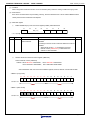
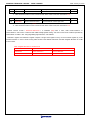
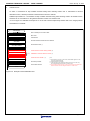
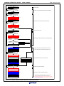
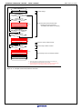
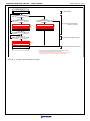
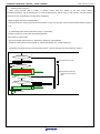
Date: Jan. 15, 2013
RENESAS TECHNICAL UPDATE
1753, Shimonumabe, Nakahara-ku, Kawasaki-shi, Kanagawa 211-8668 Japan
Renesas Electronics Corporation
Product
Category
MPU/MCU
2
I C bus interface (RIIC)
Precautions for using timeout detection function and
stop condition issuance timing when receiving master.
Title
Document
No.
TN-RX*-A048A/E
Information
Category
Technical Notification
Rev.
1.00
Lot No.
Applicable
Product
RX630 group
RX63N, RX631 group
All lots
Reference
Document
RX630 group
RX63N, RX631 group
User’s Manual, Hardware section
This is to let you know that we have revised the Technical Update which had been already issued (Issue number:
TN-RX*-A012A/E Rev.1.00, TN-RX*-A013A/E Rev.1.00). The revised portions are indicated in red letters (in flow chart,
indicated in red and blue letters).
1.
Precautions for stop condition issuance timing when receiving master
2
With I C bus interface (RIIC), one clock cycle may be inserted between the ninth clock cycle of master reception and stop
condition issuance.
When this clock affects the communication, follow the avoidance flow “Figure xx.10 Example of Master Reception
Flowchart (7-Bit Address Format)” indicated on the Page.6 of this Technical Update.
(1) Conditions
・While holding at low at the falling edge of the ninth clock cycle, writing SP=1 and reading data from ICDRR are
performed in a row.
・When data is read from ICDRR after the falling edge of the ninth clock of master reception and writing SP=1 are
detected at the same time in the RIIC.
・After SP=1 is written, when the falling edge of the ninth clock cycle of master reception and data reading from
ICDRR are detected at the same time in the RIIC.
(2) Phenomenon
One clock cycle is inserted between the ninth clock cycle of master reception and stop condition issuance.
2.
Precautions when using timeout detection function
2
While timeout detection function of I C bus interface (RIIC) is set to CMR1.CKS [2:0] ≠ 000b, timeout is detected even
when communications are proceeding correctly. To avoid this, use registered disclosed in this document and follow the
avoidance flow. In this avoidance flow, every time data is accessed, write 00h to the timeout internal counter and clear
counter.
Thus, it is applicable only to data transfer using CPU or one using DTC. When you use DMAC for data transfer of RIIC,
you need to set ICMR1.CKS [2:0] = 000b or change it to transfer using CPU or one using DTC.
(c) 2013. Renesas Electronics Corporation. All rights reserved.
Page 1 of 10
RENESAS TECHNICAL UPDATE TN-RX*-A048A/E
Date: January 15, 2013
(1) Condition
2
When using timeout detection function of I C bus interface (RIIC) under the setting of CMR1.CKS [2:0] ≠ 000.
(2) Phenomenon
Even when communications are proceeding correctly, timeout is detected from a set of ICFER.TMOE bit after a
certain period of time for detection has elapsed.
(3) Disclosed register
①
ICMR2.TMWE bit (b3) of I2C bus mode register (ICMR2) will be disclosed.
b7
b5
b6
DLCS
Bit
b3
SDDL[2:0]
0
リセット後の値
Symbol
TMWE
b4
0
0
0
b3
b2
b1
b0
TMWE
TMOH
TMOL
TMOS
0
0
0
0
Bit name
Description
R/W
Timeout internal counter
write enable bit
0: Writing to internal counter of timeout detection function is
disabled
R/W
1: Writing to internal counter of timeout detection function is
enabled
When this bit is set to “1”, the address of timeout
internal counter (TMOCNTL/U) is allocated to the
address of SARL0/SARU0.
②
Disclose the timeout internal counter register (TMOCNT).
Timeout internal counter (TMOCNT)
Address RIIC0.TMOCNTL 0008 830Ah*,
RIIC0.TMOCNTU 0008 832Ah*
RIIC1.TMOCNTL 0008 830Bh*, RIIC1.TMOCNTU 0008 832Bh*
*Same addresses with ones of the slave address registers, SARL0, SARU0. Care should be taken.
・TMOS=0 (Long mode)
Value after reset
b7
b6
b5
b4
b3
b2
b1
b0
b7
b6
b5
b4
b3
b2
b1
b0
0
0
0
0
0
0
0
0
0
0
0
0
0
0
0
0
TMOCNTU
TMOCNTL
・TMOS=1 (Short mode)
Value after reset
b7
b6
b5
b4
ー
ー
ー
ー
0
0
0
0
b3
b2
b1
b0
b7
b6
b5
b4
b3
b2
b1
b0
0
0
0
0
0
0
0
0
0
0
0
0
TMOCNTU
TMOCNTL
Page 2 of 10
RENESAS TECHNICAL UPDATE TN-RX*-A048A/E
Date: January 15, 2013
Bit
Symbol
Bit name
Description
R/W
b7-0
TMOCNTL
Timeout internal counter
Timeout internal counter low-order
W
*1
*1 : Value in timeout internal counter cannot be read. When value is read, the read value is FFh.
Bit
b7-0
Symbol
TMOCNTU
Bit name
Description
Timeout internal counter
R/W
Timeout internal counter high-order
*1
W
*2
*1 : With TMOS=1 (Short mode), b7-b4 are reserved bits. They are writable, however value written is disabled.
*2 : Value in timeout internal counter cannot be read. When value is read, the read value is FFh.
Timeout internal counter ( TMOCNTL/TMOCNTU )
is initialized (00h) after a reset, while ICCR1.IICRST=1 or
ICFER.TMOE=1 and PCLK/1 is selected with ICMR1.CKS[2:0]=000b setting, and when counter clear conditions specified by
TMOH/TMOL of ICMR2 (SCL rising edge/falling edge detection) are satisfied.
TMOCNTL register and TMOCNTU register comprise a single 16-bit register so they can be accessed together by 16-bit
transfer instruction. In case of 16-bit access, please access to the address indicated in the table “Register Allocation for 16-Bit
Access” below.
Table. Register Allocation for 16-Bit Access
Address
Upper 8 Bits
Lower 8 Bits
0008 830Ah
RIIC0.TMOCNTU
RIIC0.TMOCNTL
0008 832Ah
RIIC1.TMOCNTU
RIIC1.TMOCNTL
Page 3 of 10
RENESAS TECHNICAL UPDATE TN-RX*-A048A/E
3.
Date: January 15, 2013
Avoidance Flow
To avoid “1. Precautions for stop condition issuance timing when receiving master” and “2. Precautions for timeout
detection function”, add the procedures to the flowchart in the user’s manual.
Additional procedures for “1. Precautions for stop condition issuance timing when receiving master” are marked in blue,
and those for “2. Precautions for using timeout detection function” are marked in red.
2
“xx” as in Figure xx.5 indicates the chapter of I C of the user’s manual respectively. Please refer to the “Target products
and Reference” for details.
Initial settings
SCL and SDA pins in inactive state
ICCR1.ICE=0
RIIC reset
ICCR1.IICRST=1
Internal reset
ICCR1.ICE=1
Set SARLy and SARUy,
Set ICSER
Set slave address format and slave address
Set ICMR1.CKS[2:0]
Set ICBRL/ICBRH
Set transfer bit rate
Set ICMR2 and ICMR3
(*2)
ICMR2.TMWE=1
(*2)
TMOCNTL=00h
(*2,4)
TMOCNTU=00h
ICFER.TMOE=1
(*2)
Set ICFER
(*2)
(*1)
Timeout internal counter writing enable
(*3)
Initialization of timeout internal counter
(*3)
Timeout function enable
Set ICIER
Set interrupt enable
ICCR1.IICRST=0
Cancel internal reset
End
(*3)
y=0~2
*1. When the RIIC is used only in slave mode, set the ICBRL register to a value
longer than the data setup time.
*2. Set these registers as necessary.
*3. These steps need to be included if the timeout function is to be used. They
are not required if the timeout function is not to be used.
*4. Flowchart shows 8-bit access case. In case of 16-bit access, write 0000h to the
address indicated in the table “Register Allocation for 16-Bit Access”.
Figure xx.5 Example of RIIC Initialization Flow
Page 4 of 10
RENESAS TECHNICAL UPDATE TN-RX*-A048A/E
Date: January 15, 2013
Master transmission
[1] Initial settings
Initial settings
No
ICCR2.BBSY=0?
[2] Check I2C bus occupation and issue
a start condition.
Yes
ICCR2.ST=1
ICSR2.NACKF=0?
No
Yes
No
ICSR2.TDRE=1?
Yes
TMOCNTL=00h
TMOCNTU=00h
[3] Transmit slave address and W (first byte)
[4] Check ACK and set transmit data.
(*1,2)
Write data to ICDRT
No
All data transmitted?
Yes
No
ICSR2.TEND=1?
Yes
TMOCNTL=00h
TMOCNTU=00h
[5] Check end of last data transmission and
issue a stop condition.
(*1,2)
ICSR2.STOP=0
ICCR2.SP=1
No
[6] Check stop condition issuance.
ICSR2.STOP=1?
Yes
TMOCNTL=00h
TMOCNTU=00h
(*1,2)
[7] Processing for the next transfer operation.
ICSR2.NACKF=0
ICSR2.STOP=0
End of master transmission
*1. These steps need to be included if the timeout function is to be used.
They are not required if the timeout function is not to be used.
*2. Flowchart shows 8-bit access case. In case of 16-bit access, write
0000h to the address indicated in the table “Register Allocation for 16Bit Access”.
Figure xx.6 Example of Master Transmission Flowchart
Page 5 of 10
RENESAS TECHNICAL UPDATE TN-RX*-A048A/E
Date: January 15, 2013
Master reception
[1] Initial settings
Initial settings
No
ICCR2.BBSY=0?
[2] Check I2C bus occupation and issue a start condition.
Yes
ICCR2.ST=1
No
ICSR2.TDRE=1?
Yes
TMOCNTL=00h
(*1,2)
TMOCNTU=00h
Write data to ICDRT
No
[3] Transmit slave address and R, and check ACK.
ICSR2.RDRF=1?
Yes
TMOCNTL=00h
(*1,2)
TMOCNTU=00h
ICSR2.NACKF=0?
No
Yes
[4] Perform dummy read
Perform dummy read of ICDRR
No
ICSR2.RDRF=1?
Yes
TMOCNTL=00h
(*1,2)
TMOCNTU=00h
Next data = Final byte - 1 ?
Yes
[5] Read received data and prepare for receiving final data.
No
Next data = Final byte - 2 ?
Yes
ICMR3.WAIT=1
No
Read ICDRR
ICMR3.RDRFS=1
ICMR3.ACKBT=1
(*3)
[6] Change the timing with which RDRF is set, set nonacknowledgement, and read the last byte but one.
Read ICDRR
No
ICSR2.RDRF=1?
Yes
TMOCNTL=00h
TMOCNTU=00h
(*1,2)
ICSR2.STOP=0
ICSR2.STOP=0
SCCR2.SP=1
ICCR2.SP=1
Read ICDRR
Perform dummy read of ICDRR
[7] Read final data and issue a stop condition.
ICMR3.ACKBT=1
ICMR3.WAIT=0
No
ICSR2.STOP=1?
[8] Check stop condition issuance.
Yes
TMOCNTL=00h
TMOCNTU=00h
ICMR3.RDRFS=0
ICMR3.ACKBT=0
ICSR2.NACKF=0
ICSR2.STOP=0
End of master reception
(*1,2)
(*3)
[9] Processing for the next transfer operation.
*1. These steps need to be included if the timeout function is to be used.
They are not required if the timeout function is not to be used.
*2. Flowchart shows 8-bit access case. In case of 16-bit access, write 0000h
to the address indicated in the table “Register Allocation for 16-Bit Access”.
*3. Simultaneous writing is possible.
Figure xx.10 Example of Master Reception Flowchart (7-Bit Address Format)
Page 6 of 10
RENESAS TECHNICAL UPDATE TN-RX*-A048A/E
Date: Janury 15, 2013
Slave transmission
[1] Initial settings
Initial settings
ICSR2.NACKF=0?
No
Yes
No
ICSR2.TDRE=1?
Yes
TMOCNTL=00h
TMOCNTU=00h
(*1,2)
Write data to ICDRT
No
[2], [3] Check ACK and set transmit data.
(Checking of ACK not necessary
immediately after address is received.)
All data transmitted?
Yes
No
ICSR2.TEND=1?
Yes
TMOCNTL=00h
TMOCNTU=00h
(*1,2)
Read ICDRR
No
[4] Dummy read to release the SCL
ICSR2.STOP=1?
[5] Check stop condition issuance
Yes
TMOCNTL=00h
TMOCNTU=00h
ICSR2.NACKF=0
(*1,2)
[6] Processing for the next transfer operation.
ICSR2.STOP=0
End of slave transmission
*1. These steps need to be included if the timeout function is to be used. They
are not required if the timeout function is not to be used.
*2. Flowchart shows 8-bit access case. In case of 16-bit access, write 0000h to the
address indicated in the table “Register Allocation for 16-Bit Access”.
Figure xx.14 Example of Slave Transmission Flowchart
Page 7 of 10
RENESAS TECHNICAL UPDATE TN-RX*-A048A/E
Date: January 15, 2013
Slave reception
[1] Initial settings
Initial settings
ICSR2.STOP=0?
No
Yes
No
ICSR2.RDRF=1?
ICSR2.RDRF=1?
Yes
TMOCNTL=00h
TMOCNTU=00h
Yes
TMOCNTL=00h
(*1,2)
Read ICDRR
No
No
TMOCNTU=00h
(*1,2)
[2], [3], [4] Read receive data
(Dummy read first)
Read ICDRR (last data)
All data received?
Yes
No
ICSR2.STOP=1?
[5] Check stop condition detection
Yes
TMOCNTL=00h
TMOCNTU=00h
(*1,2)
ICSR2.STOP=0
[6] Processing for the next transfer.
End of slave reception
*1. These steps need to be included if the timeout function is to be used. They
are not required if the timeout function is not to be used.
*2. Flowchart shows 8-bit access case. In case of 16-bit access, write 0000h to the
address indicated in the table “Register Allocation for 16-Bit Access”.
Figure xx.17 Example of Slave Reception Flowchart
Page 8 of 10
RENESAS TECHNICAL UPDATE TN-RX*-A048A/E
4.
Date: January 15, 2013
Avoidance when using DTC
When writing transmit data to ICDRT or reading receive data from ICDRR by the DTC during master
transmission/reception, use the following flow to avoid the phenomenon. Set the DTC to chain transfer, and clear internal
counter every time transmit data or receive data is transferred.
Master reception flowchart is indicated below.
This flowchart shows only flow involved with DTC transfer. For the rest of the flow, refer to the flowcharts indicated on page 4
to 8.
(1) Initial settings flow: What is indicated on page 4 + DTC setting
The DTC needs to be set to enable the following operation.
Set the DTC to chain transfer.
・First chain transfer (Chain transfer 1): Write 00h to TMOCNTL and TMOCNTU.
・Subsequent chain transfer (Chain transfer 2): Transfer specified by user (Read ICDRR, etc)
(2) Example of flowchart during N-2 times transfer by DTC (excerpt comments from the flowchart on page 6)
ICSR2.NACKF=0?
No
Yes
[4] Perform dummy read.
Perform dummy read of ICDRR
No
ICSR2.RDRF=1?
Yes
TMOCNTL=00h
Chain transfer 1
TMOCNTU=00h
Next data = Final byte – 1 ?
Yes
[5] Read received data and
prepare for receiving final
data.
No
Next data = Final byte – 2 ?
No
Read ICDRR
Yes
ICMR3.WAIT=1
Chain transfer 2
Transfer by DTC
Page 9 of 10
RENESAS TECHNICAL UPDATE TN-RX*-A048A/E
Date: January 15, 2013
■Target Products and Reference
Group
RX630 group
RX63N group,
RX631 group
Title
Rev.
Document No.
Chapter of I2C
RX630 Group User’s Manual: Hardware
Rev.1.50
R01UH0040EJ0150
33
RX63N Group, RX631 Group User’s Manual: Hardware
Rev.1.50
R01UH0041EJ0150
36
Page 10 of 10