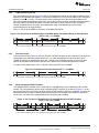
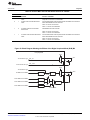
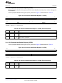
1
TMS320C642x DSP
Inter-Integrated Circuit (I2C) Peripheral
User's Guide
Literature Number: SPRUEN0D
March 2011
2
SPRUEN0D – March 2011
Submit Documentation Feedback
© 2011, Texas Instruments Incorporated
Preface ....................................................................................................................................... 6
1
Introduction ........................................................................................................................ 7
.............................................................................................. 7
.................................................................................................................. 7
1.3
Functional Block Diagram .............................................................................................. 8
1.4
Industry Standard(s) Compliance Statement ........................................................................ 8
2
Peripheral Architecture ........................................................................................................ 9
2.1
Bus Structure ............................................................................................................ 9
2.2
Clock Generation ...................................................................................................... 10
2.3
Clock Synchronization ................................................................................................. 11
2.4
Signal Descriptions .................................................................................................... 11
2.5
START and STOP Conditions ....................................................................................... 12
2.6
Serial Data Formats ................................................................................................... 13
2.7
Endianness Considerations .......................................................................................... 15
2.8
Operating Modes ....................................................................................................... 15
2.9
NACK Bit Generation .................................................................................................. 16
2.10 Arbitration ............................................................................................................... 17
2.11 Reset Considerations .................................................................................................. 18
2.12 Initialization ............................................................................................................. 18
2.13 Interrupt Support ....................................................................................................... 21
2.14 DMA Events Generated by the I2C Peripheral .................................................................... 21
2.15 Power Management ................................................................................................... 21
2.16 Emulation Considerations ............................................................................................. 22
3
Registers .......................................................................................................................... 22
3.1
I2C Own Address Register (ICOAR) ................................................................................ 23
3.2
I2C Interrupt Mask Register (ICIMR) ................................................................................ 24
3.3
I2C Interrupt Status Register (ICSTR) .............................................................................. 25
3.4
I2C Clock Divider Registers (ICCLKL and ICCLKH) .............................................................. 28
3.5
I2C Data Count Register (ICCNT) ................................................................................... 29
3.6
I2C Data Receive Register (ICDRR) ................................................................................ 30
3.7
I2C Slave Address Register (ICSAR) ............................................................................... 30
3.8
I2C Data Transmit Register (ICDXR) ............................................................................... 31
3.9
I2C Mode Register (ICMDR) ......................................................................................... 32
3.10 I2C Interrupt Vector Register (ICIVR) ............................................................................... 36
3.11 I2C Extended Mode Register (ICEMDR) ........................................................................... 37
3.12 I2C Prescaler Register (ICPSC) ..................................................................................... 38
3.13 I2C Peripheral Identification Register (ICPID1) .................................................................... 39
3.14 I2C Peripheral Identification Register (ICPID2) .................................................................... 39
Appendix A Revision History ...................................................................................................... 40
1.1
Purpose of the Peripheral
1.2
Features
SPRUEN0D – March 2011
Submit Documentation Feedback
Table of Contents
© 2011, Texas Instruments Incorporated
3
www.ti.com
List of Figures
1
I2C Peripheral Block Diagram ............................................................................................. 8
2
Multiple I2C Modules Connected ......................................................................................... 9
3
Clocking Diagram for the I2C Peripheral ............................................................................... 10
4
Synchronization of Two I2C Clock Generators During Arbitration .................................................. 11
5
Bit Transfer on the I2C-Bus .............................................................................................. 12
6
I2C Peripheral START and STOP Conditions ......................................................................... 12
7
I2C Peripheral Data Transfer ............................................................................................ 13
8
I2C Peripheral 7-Bit Addressing Format (FDF = 0, XA = 0 in ICMDR) ............................................. 13
9
I2C Peripheral 10-Bit Addressing Format With Master-Transmitter Writing to Slave-Receiver (FDF = 0,
XA = 1 in ICMDR) ......................................................................................................... 14
10
I2C Peripheral Free Data Format (FDF = 1 in ICMDR)
11
I2C Peripheral 7-Bit Addressing Format With Repeated START Condition (FDF = 0, XA = 0 in ICMDR) .... 14
12
Arbitration Procedure Between Two Master-Transmitters ........................................................... 17
13
I2C Own Address Register (ICOAR) .................................................................................... 23
14
I2C Interrupt Mask Register (ICIMR).................................................................................... 24
15
I2C Interrupt Status Register (ICSTR) .................................................................................. 25
16
I2C Clock Low-Time Divider Register (ICCLKL)
17
18
19
20
21
22
23
24
25
26
27
28
4
..............................................................
......................................................................
I2C Clock High-Time Divider Register (ICCLKH) .....................................................................
I2C Data Count Register (ICCNT).......................................................................................
I2C Data Receive Register (ICDRR) ....................................................................................
I2C Slave Address Register (ICSAR) ...................................................................................
I2C Data Transmit Register (ICDXR) ...................................................................................
I2C Mode Register (ICMDR) .............................................................................................
Block Diagram Showing the Effects of the Digital Loopback Mode (DLB) Bit .....................................
I2C Interrupt Vector Register (ICIVR) ...................................................................................
I2C Extended Mode Register (ICEMDR) ...............................................................................
I2C Prescaler Register (ICPSC) .........................................................................................
I2C Peripheral Identification Register 1 (ICPID1) .....................................................................
I2C Peripheral Identification Register 2 (ICPID2) .....................................................................
List of Figures
14
28
28
29
30
30
31
32
35
36
37
38
39
39
SPRUEN0D – March 2011
Submit Documentation Feedback
© 2011, Texas Instruments Incorporated
www.ti.com
List of Tables
................................................................................
1
Operating Modes of the I2C Peripheral
2
Ways to Generate a NACK Bit........................................................................................... 16
3
Descriptions of the I2C Interrupt Events................................................................................ 21
4
Inter-Integrated Circuit (I2C) Registers ................................................................................. 22
5
I2C Own Address Register (ICOAR) Field Descriptions
6
7
8
9
10
11
12
13
14
15
16
17
18
19
20
21
22
.............................................................
I2C Interrupt Mask Register (ICIMR) Field Descriptions .............................................................
I2C Interrupt Status Register (ICSTR) Field Descriptions............................................................
I2C Clock Low-Time Divider Register (ICCLKL) Field Descriptions ................................................
I2C Clock High-Time Divider Register (ICCLKH) Field Descriptions ...............................................
I2C Data Count Register (ICCNT) Field Descriptions ................................................................
I2C Data Receive Register (ICDRR) Field Descriptions .............................................................
I2C Slave Address Register (ICSAR) Field Descriptions ............................................................
I2C Data Transmit Register (ICDXR) Field Descriptions .............................................................
I2C Mode Register (ICMDR) Field Descriptions .......................................................................
Master-Transmitter/Receiver Bus Activity Defined by RM, STT, and STP Bits ...................................
How the MST and FDF Bits Affect the Role of TRX Bit ..............................................................
I2C Interrupt Vector Register (ICIVR) Field Descriptions ............................................................
I2C Extended Mode Register (ICEMDR) Field Descriptions.........................................................
I2C Prescaler Register (ICPSC) Field Descriptions...................................................................
I2C Peripheral Identification Register 1 (ICPID1) Field Descriptions ...............................................
I2C Peripheral Identification Register 2 (ICPID2) Field Descriptions ...............................................
Document Revision History ..............................................................................................
SPRUEN0D – March 2011
Submit Documentation Feedback
List of Tables
© 2011, Texas Instruments Incorporated
15
23
24
25
28
28
29
30
30
31
32
34
35
36
37
38
39
39
40
5
Preface
SPRUEN0D – March 2011
Read This First
About This Manual
This document describes the inter-integrated circuit (I2C) peripheral in the TMS320C642x Digital Signal
Processor (DSP). The I2C peripheral provides an interface between the DSP and other devices that are
compliant with Philips Semiconductors Inter-IC bus (I2C-bus) specification version 2.1 and connected by
way of an I2C-bus. The scope of this document assumes that you are familiar with the I2C-bus
specification.
Notational Conventions
This document uses the following conventions.
• Hexadecimal numbers are shown with the suffix h. For example, the following number is 40
hexadecimal (decimal 64): 40h.
• Registers in this document are shown in figures and described in tables.
– Each register figure shows a rectangle divided into fields that represent the fields of the register.
Each field is labeled with its bit name, its beginning and ending bit numbers above, and its
read/write properties below. A legend explains the notation used for the properties.
– Reserved bits in a register figure designate a bit that is used for future device expansion.
Related Documentation From Texas Instruments
The following documents describe the TMS320C642x Digital Signal Processor (DSP). Copies of these
documents are available on the Internet at www.ti.com. Tip: Enter the literature number in the search box
provided at www.ti.com.
The current documentation that describes the C642x DSP, related peripherals, and other technical
collateral, is available in the C6000 DSP product folder at: www.ti.com/c6000.
SPRUEM3 — TMS320C642x DSP Peripherals Overview Reference Guide. Provides an overview and
briefly describes the peripherals available on the TMS320C642x Digital Signal Processor (DSP).
SPRAA84 — TMS320C64x to TMS320C64x+ CPU Migration Guide. Describes migrating from the
Texas Instruments TMS320C64x digital signal processor (DSP) to the TMS320C64x+ DSP. The
objective of this document is to indicate differences between the two cores. Functionality in the
devices that is identical is not included.
SPRU732 — TMS320C64x/C64x+ DSP CPU and Instruction Set Reference Guide. Describes the CPU
architecture, pipeline, instruction set, and interrupts for the TMS320C64x and TMS320C64x+ digital
signal processors (DSPs) of the TMS320C6000 DSP family. The C64x/C64x+ DSP generation
comprises fixed-point devices in the C6000 DSP platform. The C64x+ DSP is an enhancement of
the C64x DSP with added functionality and an expanded instruction set.
SPRU871 — TMS320C64x+ DSP Megamodule Reference Guide. Describes the TMS320C64x+ digital
signal processor (DSP) megamodule. Included is a discussion on the internal direct memory access
(IDMA) controller, the interrupt controller, the power-down controller, memory protection, bandwidth
management, and the memory and cache.
6
Preface
SPRUEN0D – March 2011
Submit Documentation Feedback
© 2011, Texas Instruments Incorporated
User's Guide
SPRUEN0D – March 2011
Inter-Integrated Circuit (I2C) Peripheral
1
Introduction
This document describes the operation of the inter-integrated circuit (I2C) peripheral in the TMS320C642x
Digital Signal Processor (DSP). The scope of this document assumes that you are familiar with the Philips
Semiconductors Inter-IC bus (I2C-bus) specification version 2.1.
1.1
Purpose of the Peripheral
The I2C peripheral provides an interface between the TMS320C642x DSP and other devices that are
compliant with the I2C-bus specification and connected by way of an I2C-bus. External components that
are attached to this two-wire serial bus can transmit and receive data that is up to eight bits wide both to
and from the DSP through the I2C peripheral.
1.2
Features
The I2C peripheral has the following features:
• Compliance with the Philips Semiconductors I2C-bus specification (version 2.1):
– Support for byte format transfer
– 7-bit and 10-bit addressing modes
– General call
– START byte mode
– Support for multiple master-transmitters and slave-receivers mode
– Support for multiple slave-transmitters and master-receivers mode
– Combined master transmit/receive and receive/transmit mode
– I2C data transfer rate of from 10 kbps up to 400 kbps (Philips I2C rate)
• 2 to 8 bit format transfer
• Free data format mode
• One read DMA event and one write DMA event that the DMA can use
• Seven interrupts that the CPU can use
• Peripheral enable/disable capability
1.2.1
Features Not Supported
• High-speed mode
• CBUS-compatibility mode
• The combined format in 10-bit addressing mode (the I2C sends the slave address the second byte
every time it sends the slave address the first byte).
SPRUEN0D – March 2011
Submit Documentation Feedback
Inter-Integrated Circuit (I2C) Peripheral
© 2011, Texas Instruments Incorporated
7
Introduction
1.3
www.ti.com
Functional Block Diagram
A block diagram of the I2C peripheral is shown in Figure 1. Refer to Section 2 for detailed information
about the architecture of the I2C peripheral.
Figure 1. I2C Peripheral Block Diagram
I2C peripheral
Peripheral data bus
ICXSR
ICDXR
ICRSR
ICDRR
SDA
SCL
CPU
Clock
synchronizer
Control/status
registers
EDMA
Prescaler
Noise filters
Arbitrator
1.4
I2C INT
Interrupt
to CPU
ICREVT
ICXEVT
Sync events to
EDMA controller
Industry Standard(s) Compliance Statement
The I2C peripheral is compliant with the Philips Semiconductors Inter-IC bus (I2C-bus) specification
version 2.1.
8
Inter-Integrated Circuit (I2C) Peripheral
SPRUEN0D – March 2011
Submit Documentation Feedback
© 2011, Texas Instruments Incorporated
Peripheral Architecture
www.ti.com
2
Peripheral Architecture
The I2C peripheral consists of the following primary blocks:
• A serial interface: one data pin (SDA) and one clock pin (SCL)
• Data registers to temporarily hold receive data and transmit data traveling between the SDA pin and
the CPU or the EDMA controller
• Control and status registers
• A peripheral data bus interface to enable the CPU and the EDMA controller to access the I2C
peripheral registers
• A clock synchronizer to synchronize the I2C input clock (from the processor clock generator) and the
clock on the SCL pin, and to synchronize data transfers with masters of different clock speeds
• A prescaler to divide down the input clock that is driven to the I2C peripheral
• A noise filter on each of the two pins, SDA and SCL
• An arbitrator to handle arbitration between the I2C peripheral (when it is a master) and another master
• Interrupt generation logic, so that an interrupt can be sent to the CPU
• EDMA event generation logic, so that activity in the EDMA controller can be synchronized to data
reception and data transmission in the I2C peripheral
Figure 1 shows the four registers used for transmission and reception. The CPU or the EDMA controller
writes data for transmission to ICDXR and reads received data from ICDRR. When the I2C peripheral is
configured as a transmitter, data written to ICDXR is copied to ICXSR and shifted out on the SDA pin one
bit a time. When the I2C peripheral is configured as a receiver, received data is shifted into ICRSR and
then copied to ICDRR.
2.1
Bus Structure
Figure 1 shows how the I2C peripheral is connected to the I2C bus. The I2C bus is a multi-master bus
that supports a multi-master mode. This allows more than one device capable of controlling the bus that is
connected to it. A unique address recognizes each I2C device. Each I2C device can operate as either
transmitter or receiver, depending on the function of the device. Devices that are connected to the I2C bus
can be considered a master or slave when performing data transfers, in addition to being a transmitter or
receiver.
NOTE: A master device is the device that initiates a data transfer on the bus and generates the
clock signals to permit that transfer. Any device that is addressed by this master is
considered a slave during this transfer.
An example of multiple I2C modules that are connected for a two-way transfer from one device to other
devices is shown in Figure 2.
Figure 2. Multiple I2C Modules Connected
VDD
Pull-up
resistors
TI device
I2C
I2C
controller
Serial data (SDA)
Serial clock (SCL)
I2C
EPROM
SPRUEN0D – March 2011
Submit Documentation Feedback
TI device
I2C
Inter-Integrated Circuit (I2C) Peripheral
© 2011, Texas Instruments Incorporated
9
Peripheral Architecture
2.2
www.ti.com
Clock Generation
As shown in Figure 3, PLL1 receives a signal from an external clock source and produces an I2C input
clock. A programmable prescaler (IPSC bit in ICPSC) in the I2C module divides down the I2C input clock
to produce a prescaled module clock. The prescaled module clock must be operated within the range of
6.7 to 13.3 MHz. The I2C clock dividers divide-down the high (ICCH bit in ICCLKH) and low portions
(ICCL bit in ICCLKL) of the prescaled module clock signal to produce the I2C serial clock, which appears
on the SCL pin when the I2C module is configured to be a master on the I2C bus.
Figure 3. Clocking Diagram for the I2C Peripheral
External
input clock
PLL1
I2C input clock
I2C module
Register bits
(ICPSC[IPSC])
I2C
prescaler
Prescaled module clock
−−MUST be set to 6.7 to 13.3 MHz
Prescaled module clock frequency =
Register bits
(ICCLKL[ICCL]),
(ICCLKH[ICCH])
I2C input clock frequency
(IPSC + 1)
I2C clock
dividers
I2C serial clock on SCL pin
I2C serial clock frequency =
To I2C bus
prescaled module clock frequency
(ICCL + d) + (ICCH + d)
Where d depends on IPSC value in ICPSC:
IPSC value
d
0
7
1
6
2h−FFh
5
CAUTION
Prescaled Module Clock Frequency Range:
The I2C module must be operated with a prescaled module clock frequency of
6.7 to 13.3 MHz. The I2C prescaler register (ICPSC) must be configured to this
frequency range.
10
Inter-Integrated Circuit (I2C) Peripheral
SPRUEN0D – March 2011
Submit Documentation Feedback
© 2011, Texas Instruments Incorporated
Peripheral Architecture
www.ti.com
The prescaler (IPSC bit in ICPSC) must only be initialized while the I2C module is in the reset state
(IRS = 0 in ICMDR). The prescaled frequency only takes effect when the IRS bit in ICMDR is changed to
1. Changing the IPSC bit in ICPSC while IRS = 1 in ICMDR has no effect. Likewise, you must configure
the I2C clock dividers (ICCH bit in ICCLKH and ICCL bit in ICCLKL) while the I2C module is still in reset
(IRS = 0 in ICMDR).
2.3
Clock Synchronization
Only one master device generates the clock signal (SCL) under normal conditions. However, there are
two or more masters during the arbitration procedure; and, you must synchronize the clock so that you
can compare the data output. Figure 4 illustrates the clock synchronization. The wired-AND property of
SCL means that a device that first generates a low period on SCL (device #1) overrules the other devices.
At this high-to-low transition, the clock generators of the other devices are forced to start their own low
period. The SCL is held low by the device with the longest low period. The other devices that finish their
low periods must wait for SCL to be released before starting their high periods. A synchronized signal on
SCL is obtained, where the slowest device determines the length of the low period and the fastest device
determines the length of the high period.
If a device pulls down the clock line for a longer time, the result is that all clock generators must enter the
wait state. This way, a slave slows down a fast master and the slow device creates enough time to store a
received data word or to prepare a data word that you are going to transmit.
Figure 4. Synchronization of Two I2C Clock Generators During Arbitration
Wait
state
Start HIGH
period
SCL from
device #1
SCL from
device #2
Bus line
SCL
2.4
Signal Descriptions
The I2C peripheral has a serial data pin (SDA) and a serial clock pin (SCL) for data communication, as
shown in Figure 1. These two pins carry information between the C642x device and other devices that are
connected to the I2C-bus. The SDA and SCL pins both are bi-directional. They each must be connected to
a positive supply voltage using a pull-up resistor. When the bus is free, both pins are high. The driver of
these two pins has an open-drain configuration to perform the required wired-AND function.
See the device-specific data manual for additional timing and electrical specifications for these pins.
2.4.1
Input and Output Voltage Levels
The master device generates one clock pulse for each data bit that is transferred. Due to a variety of
different technology devices that can be connected to the I2C-bus, the levels of logic 0 (low) and logic 1
(high) are not fixed and depend on the associated power supply level. See the device-specific data
manual for more information.
SPRUEN0D – March 2011
Submit Documentation Feedback
Inter-Integrated Circuit (I2C) Peripheral
© 2011, Texas Instruments Incorporated
11
Peripheral Architecture
2.4.2
www.ti.com
Data Validity
The data on SDA must be stable during the high period of the clock (see Figure 5). The high or low state
of the data line, SDA, can change only when the clock signal on SCL is low.
Figure 5. Bit Transfer on the I2C-Bus
Data line
stable data
SDA
SCL
Change of data
allowed
2.5
START and STOP Conditions
The I2C peripheral can generate START and STOP conditions when the peripheral is configured to be a
master on the I2C-bus, as shown in Figure 6:
• The START condition is defined as a high-to-low transition on the SDA line while SCL is high. A
master drives this condition to indicate the start of a data transfer.
• The STOP condition is defined as a low-to-high transition on the SDA line while SCL is high. A master
drives this condition to indicate the end of a data transfer.
The I2C-bus is considered busy after a START condition and before a subsequent STOP condition. The
bus busy (BB) bit of ICSTR is 1. The bus is considered free between a STOP condition and the next
START condition. The BB is 0.
The master mode (MST) bit and the START condition (STT) bit in ICMDR must both be 1 for the I2C
peripheral to start a data transfer with a START condition. The STOP condition (STP) bit must be set to 1
for the I2C peripheral to end a data transfer with a STOP condition. A repeated START condition
generates when BB is set to 1 and STT is also set to 1. See Section 3.9 for a description of ICMDR
(including the MST, STT, and STP bits).
Figure 6. I2C Peripheral START and STOP Conditions
SDA
SCL
START
condition (S)
12
Inter-Integrated Circuit (I2C) Peripheral
STOP
condition (P)
SPRUEN0D – March 2011
Submit Documentation Feedback
© 2011, Texas Instruments Incorporated
Peripheral Architecture
www.ti.com
2.6
Serial Data Formats
Figure 7 shows an example of a data transfer on the I2C-bus. The I2C peripheral supports 1-bit to 8-bit
data values. Figure 7 is shown in an 8-bit data format (BC = 000 in ICMDR). Each bit put on the SDA line
is equivalent to one pulse on the SCL line. The data is always transferred with the most-significant bit
(MSB) first. The number of data values that can be transmitted or received is unrestricted; however, the
transmitters and receivers must agree on the number of data values being transferred.
The I2C peripheral supports the following data formats:
• 7-bit addressing mode
• 10-bit addressing mode
• Free data format mode
Figure 7. I2C Peripheral Data Transfer
Acknowledgement
bit from slave
(No-)Acknowledgement
bit from receiver
SDA
MSB
SCL
1
START
condition (S)
2
7
8
9
R/W ACK
1
2
Slave address
2.6.1
8
9
ACK
STOP
condition (P)
Data
7-Bit Addressing Format
In the 7-bit addressing format (Figure 8), the first byte after a START condition (S) consists of a 7-bit slave
address followed by a R/W bit. The R/W bit determines the direction of the data.
• R/W = 0: The master writes (transmits) data to the addressed slave.
• R/W = 1: The master reads (receives) data from the slave.
An extra clock cycle dedicated for acknowledgment (ACK) is inserted after the R/W bit. If the slave inserts
the ACK bit, n bits of data from the transmitter (master or slave, depending on the R/W bit) follow it. n is a
number from 1 to 8 that the bit count (BC) bits of ICMDR determine. The receiver inserts an ACK bit after
the data bits have been transferred.
Write a 0 to the expanded address enable (XA) bit of ICMDR to select the 7-bit addressing format.
Figure 8. I2C Peripheral 7-Bit Addressing Format (FDF = 0, XA = 0 in ICMDR)
1
7
1
1
S
Slave address
R/W
ACK
n
Data
1
n
ACK
Data
1
1
ACK P
n = The number of data bits (from 1 to 8) specified by the bit count (BC) field of ICM DR.
SPRUEN0D – March 2011
Submit Documentation Feedback
Inter-Integrated Circuit (I2C) Peripheral
© 2011, Texas Instruments Incorporated
13
Peripheral Architecture
2.6.2
www.ti.com
10-Bit Addressing Format
The 10-bit addressing format (Figure 9) is like the 7-bit addressing format, but the master sends the slave
address in two separate byte transfers. The first byte consists of 11110b, the two MSBs of the 10-bit slave
address, and R/W = 0 (write). The second byte is the remaining 8 bits of the 10-bit slave address. The
slave must send acknowledgment (ACK) after each of the two byte transfers. Once the master has written
the second byte to the slave, the master can either write data or use a repeated START condition to
change the data direction. (For more information about using 10-bit addressing, see the Philips
Semiconductors I2C-bus specification.)
Write 1 to the XA bit of ICMDR to select the 10-bit addressing format.
Figure 9. I2C Peripheral 10-Bit Addressing Format With Master-Transmitter Writing to Slave-Receiver
(FDF = 0, XA = 1 in ICMDR)
1
7
1
S
11110AA
0
A A = 2 MSBs
R/W
1
8
1
ACK
AAAAAAAA
ACK
1
n
Data
1
ACK P
8 LSBs of slave address
n = The number of data bits (from 1 to 8) specified by the bit count (BC) field of ICMDR.
2.6.3
Free Data Format
In the free data format (Figure 10), the first bits after a START condition (S) are a data word. An ACK bit is
inserted after each data word, which can be from 1 to 8 bits, depending on the bit count (BC) bits of
ICMDR. No address or data-direction bit is sent. Therefore, the transmitter and the receiver must both
support the free data format, and the direction of the data must be constant throughout the transfer.
To select the free data format, write 1 to the free data format (FDF) bit of ICMDR.
Figure 10. I2C Peripheral Free Data Format (FDF = 1 in ICMDR)
1
n
1
n
1
S
Data
ACK
Data
ACK
1
n
Data
1
ACK P
n = The number of data bits (from 1 to 8) specified by the bit count (BC) field of ICMDR.
2.6.4
Using a Repeated START Condition
The repeated START condition can be used with the 7-bit addressing, 10-bit addressing, and free data
formats. The 7-bit addressing format using a repeated START condition (S) is shown in Figure 11. At the
end of each data word, the master can drive another START condition. Using this capability, a master can
transmit/receive any number of data words before driving a STOP condition. The length of a data word
can be from 1 to 8 bits and is selected with the bit count (BC) bits of ICMDR.
Figure 11. I2C Peripheral 7-Bit Addressing Format With Repeated START Condition
(FDF = 0, XA = 0 in ICMDR)
1
S
1
7
1
Slave address R/W ACK
1
n
1
1
7
Data
ACK
S
Slave address
Any
number
1
1
R/W ACK
1
n
1
1
Data
ACK
P
Any number
n = The number of data bits (from 1 to 8) specified by the bit count (BC) field of ICMDR.
14
Inter-Integrated Circuit (I2C) Peripheral
SPRUEN0D – March 2011
Submit Documentation Feedback
© 2011, Texas Instruments Incorporated
Peripheral Architecture
www.ti.com
2.7
Endianness Considerations
When the device is configured for big-endian mode, in order for the data to be placed in the right side of
the register being accessed, access to the I2C registers must be performed as follows:
• 8-bit accesses: An offset of 3h must be added to the address of the register being accessed. For
example, the offset address of ICDRR becomes 1Bh (18h + 3h).
• 16-bit accesses: Not supported for the I2C peripheral.
• 32-bit accesses: No offset is needed. For example, the offset address of ICDRR remains as 18h.
In general, software programs the CPU to use 32-bit reads and writes when accessing the I2C registers;
therefore, no offset is needed. However, software usually programs the EDMA to read and write 8-bit
values from the ICDDR and ICDXR registers; hence, the offset must be added.
No offset is needed to access the I2C registers when the device is configured in little-endian mode.
2.8
Operating Modes
The I2C peripheral has four basic operating modes to support data transfers as a master and as a slave.
See Table 1 for the names and descriptions of the modes.
If the I2C peripheral is a master, it begins as a master-transmitter and, typically, transmits an address for a
particular slave. When giving data to the slave, the I2C peripheral must remain a master-transmitter. In
order to receive data from a slave, the I2C peripheral must be changed to the master-receiver mode.
If the I2C peripheral is a slave, it begins as a slave-receiver and, typically, sends acknowledgment when it
recognizes its slave address from a master. If the master will be sending data to the I2C peripheral, the
peripheral must remain a slave-receiver. If the master has requested data from the I2C peripheral, the
peripheral must be changed to the slave-transmitter mode.
Table 1. Operating Modes of the I2C Peripheral
Operating Mode
Description
Slave-receiver mode
The I2C peripheral is a slave and receives data from a master. All slave modules begin in this
mode. In this mode, serial data bits received on SDA are shifted in with the clock pulses that are
generated by the master. As a slave, the I2C peripheral does not generate the clock signal, but it
can hold SCL low while the intervention of the processor is required (RSFULL = 1 in ICSTR) after
data has been received.
Slave-transmitter mode
The I2C peripheral is a slave and transmits data to a master. This mode can only be entered from
the slave-receiver mode; the I2C peripheral must first receive a command from the master. When
you are using any of the 7-bit/10-bit addressing formats, the I2C peripheral enters its
slave-transmitter mode if the slave address is the same as its own address (in ICOAR) and the
master has transmitted R/W = 1. As a slave-transmitter, the I2C peripheral then shifts the serial
data out on SDA with the clock pulses that are generated by the master. While a slave, the I2C
peripheral does not generate the clock signal, but it can hold SCL low while the intervention of the
processor is required (XSMT = 0 in ICSTR) after data has been transmitted.
Master-receiver mode
The I2C peripheral is a master and receives data from a slave. This mode can only be entered
from the master-transmitter mode; the I2C peripheral must first transmit a command to the slave.
When you are using any of the 7-bit/10-bit addressing formats, the I2C peripheral enters its
master-receiver mode after transmitting the slave address and R/W = 1. Serial data bits on SDA
are shifted into the I2C peripheral with the clock pulses generated by the I2C peripheral on SCL.
The clock pulses are inhibited and SCL is held low when the intervention of the processor is
required (RSFULL = 1 in ICSTR) after data has been received.
Master-transmitter mode
The I2C peripheral is a master and transmits control information and data to a slave. All master
modules begin in this mode. In this mode, data assembled in any of the 7-bit/10-bit addressing
formats is shifted out on SDA. The bit shifting is synchronized with the clock pulses generated by
the I2C peripheral on SCL. The clock pulses are inhibited and SCL is held low when the
intervention of the processor is required (XSMT = 0 in ICSTR) after data has been transmitted.
SPRUEN0D – March 2011
Submit Documentation Feedback
Inter-Integrated Circuit (I2C) Peripheral
© 2011, Texas Instruments Incorporated
15
Peripheral Architecture
2.9
www.ti.com
NACK Bit Generation
When the I2C peripheral is a receiver (master or slave), it can acknowledge or ignore bits sent by the
transmitter. To ignore any new bits, the I2C peripheral must send a no-acknowledge (NACK) bit during the
acknowledge cycle on the bus. Table 2 summarizes the various ways the I2C peripheral sends a NACK
bit.
Table 2. Ways to Generate a NACK Bit
NACK Bit Generation
I2C Peripheral
Condition
Basic
Slave-receiver mode
Optional
• Disable data transfers (STT = 0 in ICSTR).
• Allow an overrun condition (RSFULL = 1 in
ICSTR).
• Reset the peripheral (IRS = 0 in ICMDR)
Set the NACKMOD bit of ICMDR before the rising
edge of the last data bit you intend to receive.
Master-receiver mode
AND
Repeat mode
(RM = 1 in ICMDR)
• Generate a STOP condition (STOP = 1 in
ICMDR).
• Reset the peripheral (IRS = 0 in ICMDR).
Set the NACKMOD bit of ICMDR before the rising
edge of the last data bit you intend to receive.
Master-receiver mode
AND
Nonrepeat mode
(RM = 0 in ICMDR)
• If STP = 1 in ICMDR, allow the internal data
counter to count down to 0 and force a STOP
condition.
• If STP = 0, make STP = 1 to generate a
STOP condition.
• Reset the peripheral (IRS = 0 in ICMDR).
Set the NACKMOD bit of ICMDR before the rising
edge of the last data bit you intend to receive.
.
16
Inter-Integrated Circuit (I2C) Peripheral
SPRUEN0D – March 2011
Submit Documentation Feedback
© 2011, Texas Instruments Incorporated
Peripheral Architecture
www.ti.com
2.10 Arbitration
If two or more master-transmitters simultaneously start a transmission on the same bus, an arbitration
procedure is invoked. The arbitration procedure uses the data presented on the serial data bus (SDA) by
the competing transmitters. Figure 12 illustrates the arbitration procedure between two devices. The first
master-transmitter, which drives SDA high, is overruled by another master-transmitter that drives SDA low.
The arbitration procedure gives priority to the device that transmits the serial data stream with the lowest
binary value. Should two or more devices send identical first bytes, arbitration continues on the
subsequent bytes.
If the I2C peripheral is the losing master, it switches to the slave-receiver mode, sets the arbitration lost
(AL) flag, and generates the arbitration-lost interrupt.
If during a serial transfer the arbitration procedure is still in progress when a repeated START condition or
a STOP condition is transmitted to SDA, the master-transmitters involved must send the repeated START
condition or the STOP condition at the same position in the format frame. Arbitration is not allowed
between:
• A repeated START condition and a data bit
• A STOP condition and a data bit
• A repeated START condition and a STOP condition
Figure 12. Arbitration Procedure Between Two Master-Transmitters
Bus line
SCL
Device #1 lost arbitration
and switches off
Data from
device #1
1
0
Data from
device #2
1
0
0
1
0
1
Bus line
SDA
1
0
0
1
0
1
SPRUEN0D – March 2011
Submit Documentation Feedback
Inter-Integrated Circuit (I2C) Peripheral
© 2011, Texas Instruments Incorporated
17
Peripheral Architecture
www.ti.com
2.11 Reset Considerations
The I2C peripheral has two reset sources: software reset and hardware reset.
2.11.1
Software Reset Considerations
To reset the I2C peripheral, write 0 to the I2C reset (IRS) bit in the I2C mode register (ICMDR). All status
bits in the I2C interrupt status register (ICSTR) are forced to their default values, and the I2C peripheral
remains disabled until IRS is changed to 1. The SDA and SCL pins are in the high-impedance state.
NOTE:
2.11.2
If the IRS bit is cleared to 0 during a transfer, this can cause the I2C bus to hang (SDA and
SCL are in the high-impedance state).
Hardware Reset Considerations
When a hardware reset occurs, all the registers of the I2C peripheral are set to their default values and
the I2C peripheral remains disabled until the I2C reset (IRS) bit in the I2C mode register (ICMDR) is
changed to 1.
NOTE:
The IRS bit must be cleared to 0 while you configure/reconfigure the I2C peripheral.
Forcing IRS to 0 can be used to save power and to clear error conditions.
2.12 Initialization
Proper I2C initialization is required prior to starting communication with other I2C device(s). Unless a fully
fledged driver is in place, you need to determine the required I2C configuration needed (for example,
Master Receiver, etc.) and configure the I2C controller with the desired settings. Enabling the I2C clock
should be the first task. Then the I2C controller is placed in reset. You now are ready to configure the I2C
controller. Once configuration is done, you need to enable the I2C controller by releasing the controller
from reset. Prior to starting communication, you need to make sure that all status bits are cleared and no
pending interrupts exist. Once the bus is determined to be available (the bus is not busy), the I2C is ready
to proceed with the desired communication.
18
Inter-Integrated Circuit (I2C) Peripheral
SPRUEN0D – March 2011
Submit Documentation Feedback
© 2011, Texas Instruments Incorporated
Peripheral Architecture
www.ti.com
2.12.1
Configuring the I2C in Master Receiver Mode and Servicing Receive Data via CPU
The following initialization procedure is for the I2C controller configured in Master Receiver mode. The
CPU is used to move data from the I2C receive register to CPU memory (memory accessible by the
CPU).
1. Enable I2C clock from the Power and Sleep Controller (see the TMS320C642x DSP Power and Sleep
Controller (PSC) User's Guide (SPRUEN8)).
2. Place I2C in reset (clear IRS = 0 in ICMDR).
3. Configure ICMDR:
• Configure I2C as Master (MST = 1).
• Indicate the I2C configuration to be used; for example, Data Receiver (TRX = 0)
• Indicate 7-bit addressing is to be used (XA = 0).
• Disable repeat mode (RM = 0).
• Disable loopback mode (DLB = 0).
• Disable free data format (FDF = 0).
• Optional: Disable start byte mode if addressing a fully fledged I2C device (STB = 0).
• Set number of bits to transfer to be 8 bits (BC = 0).
4. Configure Slave Address: the I2C device this I2C master would be addressing (ICSAR = 7BIT
ADDRESS).
5. Configure the peripheral clock operation frequency (ICPSC). This value should be selected in such a
way that the frequency is between 6.7 and 13.3 MHz.
6. Configure I2C master clock frequency:
• Configure the low-time divider value (ICCLKL).
• Configure the high-time divider value (ICCLKH).
7. Make sure the interrupt status register (ICSTR) is cleared:
• Read ICSTR and write it back (write 1 to clear) ICSTR = ICSTR
• Read ICIVR until it is 0.
8. Take I2C controller out of reset: enable I2C controller (set IRS bit = 1 in ICMDR).
9. Wait until bus busy bit is cleared (BB = 0 in ICSTR).
10. Generate a START event, followed by Slave Address, etc. (set STT = 1 in ICMDR).
11. Wait until data is received (ICRRDY = 1 in ICSTR).
12. Read data:
• If ICRRDY = 1 in ICSTR, then read ICDRR.
• Perform the previous two steps until receiving one byte short of the entire byte expecting to
receive.
13. Configure the I2C controller not to generate an ACK on the next/final byte reception: set NACKMOD
bit for the I2C to generate a NACK on the last byte received (set NACKMOD = 1 in ICMDR).
14. End transfer/release bus when transfer is done. Generate a STOP event (set STP = 1 in ICMDR).
2.12.2
Configuring the I2C in Slave Receiver and Transmitter Mode
The following initialization procedure is for the I2C controller configured in Slave Receiver and Transmitter
mode.
1. Enable I2C clock from PSC Level. Do this so that you will be able to configure the I2C registers.
2. Place I2C in reset (clear IRS = 0 in ICMDR).
3. Assign the Address (a 7 bit or 10 bit address) that the I2C Controller will be responding to. This is the
Address that the Master is going to broadcast when attempting to start communication with this slave
device; I2C Controller.
• If the I2C is able to respond to 7-bit Addressing: Configure XA = 0
• If the I2C is able to respond to 10-bit Addressing: Configure XA = 1
• Program ICOAR = Assigned Address (7-bit or 10-bit Address)
SPRUEN0D – March 2011
Submit Documentation Feedback
Inter-Integrated Circuit (I2C) Peripheral
© 2011, Texas Instruments Incorporated
19
Peripheral Architecture
www.ti.com
4. Enable the desired interrupt you need to receive by setting the desired interrupt bit field within ICIMR
to enable the particular Interrupt.
• AAS = 1; Expect an interrupt when Master's Address matches yours (ICOAR programmed value).
• ICRRDY = 1; Expect a receive interrupt when a byte worth data sent from the master is ready to
be read.
• ICXRDY = 1; Expect to receive interrupt when the transmit register is ready to be written with a
new data that is to be sent to the master.
• SCD = 1; Expect to receive interrupt when Stop Condition is detected.
5. Configure the I2C Controller Operating frequency; this is not the serial clock frequency. This should be
between 6.7 and 13.3 MHz. Program IPSC to generate a 6.7 to 13.3 MHz operating frequency.
• Prescaled Module Clock Frequency = PLL1 Output Frequency / (IPSC + 1).
6. Configure the I2C Serial Clock Frequency. It is advised to configure this frequency to operate at
400 kHz. This will allow the slave device to be able to attend to all Master speeds. Program ICCH and
ICCL.
• 400 kHz = I2C Operating Frequency (6.7 to 13.3 MHz from Step 5) / [(ICCH + 5) + (ICCL + 5)].
• If ICCL == ICCH ≥ 400 kHz = Prescaled Module Clock Frequency / [2 × ICCH + 10]
7. Configure the Mode Register.
• MST = 0; Configure the I2C Controller to operate as SLAVE.
• FDF = 0; Free Data Format is disabled.
• BC = 0; Set data width to 8 bytes.
• DLB = 0; Disable Loopback Mode.
• STB = 0; I2C Controller can detect Start condition via hardware.
• RM = 1, STP = 0, STT = 0. See Table 15 (No Activity case).
• Configure remaining bits other than IRS to 0.
8. Release I2C from Reset
• IRS = 1; Make sure you do not over write your previous configurations.
9. Make sure Interrupt Status Register is cleared.
• ICSTR = ICSTR; Clear Interrupt fields that require writing '1' requirements.
• While (ICIVR != 0) Read ICIVR; Read until it is cleared to 0.
10. Instruct I2C Controller to detect START Condition and Its Own Address.
• STT = 1; Make sure you do not over write your previous configurations.
11. MASTER desires to perform a write transfer. If Master requests a Write, I2C needs to receive data,
perform the following:
• Wait for Receive Interrupt to be received, ICRRDY = 1.
• Read Data
12. Perform Step 11 until one of the two happens:
• Master generates a STOP Condition (SCD = 1) or
• I2C Slave desires to end receive transfer.
If the latter, then the I2C needs to Not Acknowledge the last byte to be received from the Master.
After reading the byte prior from the last byte set NACKMOD bit so that the I2C automatically
NACKs the following received data byte, which is the last data byte.
• NACKMOD = 1; set this field on the 2nd data prior from the last.
13. Master desires to perform a read transfer. If Master requests a Read, I2C needs to transmit data,
perform the following:
• Write Data.
• Wait for Transmit Interrupt to be received, ICXRDY = 1.
14. Perform step 13 until a STOP condition is detected (SCD = 1).
20
Inter-Integrated Circuit (I2C) Peripheral
SPRUEN0D – March 2011
Submit Documentation Feedback
© 2011, Texas Instruments Incorporated
Peripheral Architecture
www.ti.com
2.13 Interrupt Support
The is capable of interrupting the DSP CPU. The CPU can determine which I2C events caused the
interrupt by reading the I2C interrupt vector register (ICIVR). ICIVR contains a binary-coded interrupt
vector type to indicate which interrupt has occurred. Reading ICIVR clears the interrupt flag; if other
interrupts are pending, a new interrupt is generated. If there is more than one pending interrupt flag,
reading ICIVR clears the highest-priority interrupt flag.
2.13.1
Interrupt Events and Requests
The I2C peripheral can generate the interrupts described in Table 3. Each interrupt has a flag bit in the
I2C interrupt status register (ICSTR) and a mask bit in the interrupt mask register (ICIMR). When one of
the specified events occurs, its flag bit is set. If the corresponding mask bit is 0, the interrupt request is
blocked; if the mask bit is 1, the request is forwarded to the CPU as an I2C interrupt.
Table 3. Descriptions of the I2C Interrupt Events
2.13.2
I2C Interrupt
Initiating Event
Arbitration-lost interrupt (AL)
Generated when the I2C arbitration procedure is lost or illegal START/STOP conditions
occur
No-acknowledge interrupt (NACK)
Generated when the master I2C does not receive any acknowledge from the receiver
Registers-ready-for-access interrupt
(ARDY)
Generated by the I2C when the previously programmed address, data and command have
been performed and the status bits have been updated. This interrupt is used to let the
controlling processor know that the I2C registers are ready to be accessed.
Receive interrupt/status (ICRINT
and ICRRDY)
Generated when the received data in the receive-shift register (ICRSR) has been copied into
the ICDRR. The ICRRDY bit can also be polled by the CPU to read the received data in the
ICDRR.
Transmit interrupt/status (ICXINT
and ICXRDY)
Generated when the transmitted data has been copied from ICDXR to the transmit-shift
register (ICXSR) and shifted out on the SDA pin. This bit can also polled by the CPU to write
the next transmitted data into the ICDXR.
Stop-Condition-Detection interrupt
(SCD)
Generated when a STOP condition has been detected
Address-as-Slave interrupt (AAS)
Generated when the I2C has recognized its own slave address or an address of all (8)
zeros.
Interrupt Multiplexing
The I2C interrupt to the DSP CPU are not multiplexed with any other interrupt source.
2.14 DMA Events Generated by the I2C Peripheral
For the EDMA controller to handle transmit and receive data, the I2C peripheral generates the following
two EDMA events. Activity in EDMA channels can be synchronized to these events.
• Receive event (ICREVT): When receive data has been copied from the receive shift register (ICRSR)
to the data receive register (ICDRR), the I2C peripheral sends an REVT signal to the EDMA controller.
In response, the EDMA controller can read the data from ICDRR.
• Transmit event (ICXEVT): When transmit data has been copied from the data transmit register
(ICDXR) to the transmit shift register (ICXSR), the I2C peripheral sends an XEVT signal to the EDMA
controller. In response, the EDMA controller can write the next transmit data value to ICDXR.
2.15 Power Management
The I2C peripheral can be placed in reduced-power modes to conserve power during periods of low
activity. The power management of the I2C peripheral is controlled by the processor Power and Sleep
Controller (PSC). The PSC acts as a master controller for power management for all of the peripherals on
the device. For detailed information on power management procedures using the PSC, see the
TMS320C642x DSP Power and Sleep Controller (PSC) User's Guide (SPRUEN8).
SPRUEN0D – March 2011
Submit Documentation Feedback
Inter-Integrated Circuit (I2C) Peripheral
© 2011, Texas Instruments Incorporated
21
Registers
www.ti.com
2.16 Emulation Considerations
The response of the I2C events to emulation suspend events (such as halts and breakpoints) is controlled
by the FREE bit in the I2C mode register (ICMDR). The I2C peripheral either stops exchanging data
(FREE = 0) or continues to run (FREE = 1) when an emulation suspend event occurs. How the I2C
peripheral terminates data transactions is affected by whether the I2C peripheral is acting as a master or a
slave. For more information, see the description of the FREE bit in ICMDR (see Section 3.9).
3
Registers
Table 4 lists the memory-mapped registers for the inter-integrated circuit (I2C) peripheral. See the
device-specific data manual for the memory address of these registers. All other register offset addresses
not listed in Table 4 should be considered as reserved locations and the register contents should not be
modified.
Table 4. Inter-Integrated Circuit (I2C) Registers
Offset
22
Acronym
Register Description
0h
ICOAR
I2C Own Address Register
Section 3.1
Section
4h
ICIMR
I2C Interrupt Mask Register
Section 3.2
8h
ICSTR
I2C Interrupt Status Register
Section 3.3
Ch
ICCLKL
I2C Clock Low-Time Divider Register
Section 3.4
10h
ICCLKH
I2C Clock High-Time Divider Register
Section 3.4
14h
ICCNT
I2C Data Count Register
Section 3.5
18h
ICDRR
I2C Data Receive Register
Section 3.6
1Ch
ICSAR
I2C Slave Address Register
Section 3.7
20h
ICDXR
I2C Data Transmit Register
Section 3.8
24h
ICMDR
I2C Mode Register
Section 3.9
28h
ICIVR
I2C Interrupt Vector Register
Section 3.10
2Ch
ICEMDR
I2C Extended Mode Register
Section 3.11
30h
ICPSC
I2C Prescaler Register
Section 3.12
34h
ICPID1
I2C Peripheral Identification Register 1
Section 3.13
38h
ICPID2
I2C Peripheral Identification Register 2
Section 3.13
Inter-Integrated Circuit (I2C) Peripheral
SPRUEN0D – March 2011
Submit Documentation Feedback
© 2011, Texas Instruments Incorporated
Registers
www.ti.com
3.1
I2C Own Address Register (ICOAR)
The I2C own address register (ICOAR) is used to specify its own slave address, which distinguishes it
from other slaves connected to the I2C-bus. If the 7-bit addressing mode is selected (XA = 0 in ICMDR),
only bits 6-0 are used; bits 9-7 are ignored.
The I2C own address register (ICOAR) is shown in Figure 13 and described in Table 5.
Figure 13. I2C Own Address Register (ICOAR)
31
16
Reserved
R-0
15
10
9
0
Reserved
OADDR
R-0
R/W-0
LEGEND: R/W = Read/Write; R = Read only; -n = value after reset
Table 5. I2C Own Address Register (ICOAR) Field Descriptions
Bit
31-10
9-0
Field
Reserved
OADDR
Value
0
Description
These reserved bit locations are always read as zeros. A value written to this field has no effect.
0-3FFh Own slave address. Provides the slave address of the I2C.
In 7-bit addressing mode (XA = 0 in ICMDR): bits 6-0 provide the 7-bit slave address of the I2C. Bits 9-7
are ignored.
In 10-bit addressing mode (XA = 1 in ICMDR): bits 9-0 provide the 10-bit slave address of the I2C.
SPRUEN0D – March 2011
Submit Documentation Feedback
Inter-Integrated Circuit (I2C) Peripheral
© 2011, Texas Instruments Incorporated
23
Registers
3.2
www.ti.com
I2C Interrupt Mask Register (ICIMR)
The I2C interrupt mask register (ICIMR) is used to individually enable or disable I2C interrupt requests.
The I2C interrupt mask register (ICIMR) is shown in Figure 14 and described Table 6.
Figure 14. I2C Interrupt Mask Register (ICIMR)
31
8
Reserved
R-0
7
6
5
4
3
2
1
0
Reserved
AAS
SCD
ICXRDY
ICRRDY
ARDY
NACK
AL
R-0
R/W-0
R/W-0
R/W-0
R/W-0
R/W-0
R/W-0
R/W-0
LEGEND: R/W = Read/Write; R = Read only; -n = value after reset
Table 6. I2C Interrupt Mask Register (ICIMR) Field Descriptions
Bit
31-7
6
5
4
3
2
1
0
24
Field
Reserved
Value
0
AAS
Description
These reserved bit locations are always read as zeros. A value written to this field has no effect.
Address-as-slave interrupt enable bit.
0
Interrupt request is disabled.
1
Interrupt request is enabled.
SCD
Stop condition detected interrupt enable bit.
0
Interrupt request is disabled.
1
Interrupt request is enabled.
ICXRDY
Transmit-data-ready interrupt enable bit.
0
Interrupt request is disabled.
1
Interrupt request is enabled.
ICRRDY
Receive-data-ready interrupt enable bit.
0
Interrupt request is disabled.
1
Interrupt request is enabled.
ARDY
Register-access-ready interrupt enable bit.
0
Interrupt request is disabled.
1
Interrupt request is enabled.
NACK
No-acknowledgment interrupt enable bit.
0
Interrupt request is disabled.
1
Interrupt request is enabled.
AL
Arbitration-lost interrupt enable bit
0
Interrupt request is disabled.
1
Interrupt request is enabled.
Inter-Integrated Circuit (I2C) Peripheral
SPRUEN0D – March 2011
Submit Documentation Feedback
© 2011, Texas Instruments Incorporated
Registers
www.ti.com
3.3
I2C Interrupt Status Register (ICSTR)
The I2C interrupt status register (ICSTR) is used to determine which interrupt has occurred and to read
status information.
The I2C interrupt status register (ICSTR) is shown in Figure 15 and described in Table 7.
Figure 15. I2C Interrupt Status Register (ICSTR)
31
16
Reserved
R-0
15
14
13
12
11
10
9
8
Reserved
SDIR
NACKSNT
BB
RSFULL
XSMT
AAS
AD0
R-0
R/W1C-0
R/W1C-0
R/W1C-0
R-0
R-1
R-0
R-0
7
5
4
3
2
1
0
Reserved
6
SCD
ICXRDY
ICRRDY
ARDY
NACK
AL
R-0
R/W1C-0
R/W1C-1
R/W1C-0
R/W1C-0
R/W1C-0
R/W1C-0
LEGEND: R/W = Read/Write; R = Read only; W1C = Write 1 to clear (writing 0 has no effect); -n = value after reset
Table 7. I2C Interrupt Status Register (ICSTR) Field Descriptions
Bit
31-15
14
Field
Reserved
Value
0
SDIR
Description
These reserved bit locations are always read as zeros. A value written to this field has no effect.
Slave direction bit. In digital-loopback mode (DLB), the SDIR bit is cleared to 0.
0
I2C is acting as a master-transmitter/receiver or a slave-receiver. SDIR is cleared by one of the
following events:
• A STOP or a START condition.
• SDIR is manually cleared. To clear this bit, write a 1 to it.
1
13
NACKSNT
I2C is acting as a slave-transmitter.
No-acknowledgment sent bit. NACKSNT bit is used when the I2C is in the receiver mode. One instance
in which NACKSNT is affected is when the NACK mode is used (see the description for NACKMOD in
Section 3.9).
0
NACK is not sent. NACKSNT is cleared by one of the following events:
• It is manually cleared. To clear this bit, write a 1 to it.
• The I2C is reset (either when 0 is written to the IRS bit of ICMDR or when the processor is reset).
1
12
BB
NACK is sent. A no-acknowledge bit was sent during the acknowledge cycle on the I2C-bus.
Bus busy bit. BB bit indicates whether the I2C-bus is busy or is free for another data transfer. In the
master mode, BB is controlled by the software.
0
Bus is free. BB is cleared by one of the following events:
• The I2C receives or transmits a STOP bit (bus free).
• BB is manually cleared. To clear this bit, write a 1 to it.
• The I2C is reset (either when 0 is written to the IRS bit of ICMDR or when the processor is reset).
1
Bus is busy. When the STT bit in ICMDR is set to 1, a restart condition is generated. BB is set by one of
the following events:
• The I2C has received or transmitted a START bit on the bus.
• SCL is in a low state and the IRS bit in ICMDR is 0.
11
RSFULL
Receive shift register full bit. RSFULL indicates an overrun condition during reception. Overrun occurs
when the receive shift register (ICRSR) is full with new data but the previous data has not been read
from the data receive register (ICDRR). The new data will not be copied to ICDRR until the previous
data is read. As new bits arrive from the SDA pin, they overwrite the bits in ICRSR.
0
No overrun is detected. RSFULL is cleared by one of the following events:
• ICDRR is read.
• The I2C is reset (either when 0 is written to the IRS bit of ICMDR or when the processor is reset).
1
Overrun is detected.
SPRUEN0D – March 2011
Submit Documentation Feedback
Inter-Integrated Circuit (I2C) Peripheral
© 2011, Texas Instruments Incorporated
25
Registers
www.ti.com
Table 7. I2C Interrupt Status Register (ICSTR) Field Descriptions (continued)
Bit
Field
10
XSMT
Value
Description
Transmit shift register empty bit. XSMT indicates that the transmitter has experienced underflow.
Underflow occurs when the transmit shift register (ICXSR) is empty but the data transmit register
(ICDXR) has not been loaded since the last ICDXR-to-ICXSR transfer. The next ICDXR-to-ICXSR
transfer will not occur until new data is in ICDXR. If new data is not transferred in time, the previous
data may be re-transmitted on the SDA pin.
0
Underflow is detected.
1
No underflow is detected. XSMT is set by one of the following events:
• Data is written to ICDXR.
• The I2C is reset (either when 0 is written to the IRS bit of ICMDR or when the processor is reset).
9
AAS
Addressed-as-slave bit.
0
The AAS bit has been cleared by a repeated START condition or by a STOP condition.
1
AAS is set by one of the following events:
• I2C has recognized its own slave address or an address of all zeros (general call).
• The first data word has been received in the free data format (FDF = 1 in ICMDR).
8
7-6
5
AD0
Reserved
Address 0 bit.
0
AD0 has been cleared by a START or STOP condition.
1
An address of all zeros (general call) is detected.
0
These reserved bit locations are always read as zeros. A value written to this field has no effect.
SCD
Stop condition detected bit. SCD indicates when a STOP condition has been detected on the I2C bus.
The STOP condition could be generated by the I2C or by another I2C device connected to the bus.
0
No STOP condition has been detected. SCD is cleared by one of the following events:
• By reading the INTCODE bits in ICIVR as 110b.
• SCD is manually cleared. To clear this bit, write a 1 to it.
1
4
ICXRDY
A STOP condition has been detected.
Transmit-data-ready interrupt flag bit. ICXRDY indicates that the data transmit register (ICDXR) is ready
to accept new data because the previous data has been copied from ICDXR to the transmit shift
register (ICXSR). The CPU can poll ICXRDY or use the XRDY interrupt request.
0
ICDXR is not ready. ICXRDY is cleared by one of the following events:
• Data is written to ICDXR.
• ICXRDY is manually cleared. To clear this bit, write a 1 to it.
1
3
ICRRDY
ICDXR is ready. Data has been copied from ICDXR to ICXSR. ICXRDY is forced to 1 when the I2C is
reset.
Receive-data-ready interrupt flag bit. ICRRDY indicates that the data receive register (ICDRR) is ready
to be read because data has been copied from the receive shift register (ICRSR) to ICDRR. The CPU
can poll ICRRDY or use the RRDY interrupt request.
0
ICDRR is not ready. ICRRDY is cleared by one of the following events:
• ICDRR is read.
• ICRRDY is manually cleared. To clear this bit, write a 1 to it.
• The I2C is reset (either when 0 is written to the IRS bit of ICMDR or when the processor is reset).
1
2
ARDY
ICDRR is ready. Data has been copied from ICRSR to ICDRR.
Register-access-ready interrupt flag bit (only applicable when the I2C is in the master mode). ARDY
indicates that the I2C registers are ready to be accessed because the previously programmed address,
data, and command values have been used. The CPU can poll ARDY or use the ARDY interrupt
request.
0
The registers are not ready to be accessed. ARDY is cleared by one of the following events:
• The I2C starts using the current register contents.
• ARDY is manually cleared. To clear this bit, write a 1 to it.
• The I2C is reset (either when 0 is written to the IRS bit of ICMDR or when the processor is reset).
1
The registers are ready to be accessed. This bit is set after the slave address appears on the I2C bus.
• In the nonrepeat mode (RM = 0 in ICMDR): If STP = 0 in ICMDR, ARDY is set when the internal data
counter counts down to 0. If STP = 1, ARDY is not affected (instead, the I2C generates a STOP
condition when the counter reaches 0).
• In the repeat mode (RM = 1): ARDY is set at the end of each data word transmitted from ICDXR.
26
Inter-Integrated Circuit (I2C) Peripheral
SPRUEN0D – March 2011
Submit Documentation Feedback
© 2011, Texas Instruments Incorporated
Registers
www.ti.com
Table 7. I2C Interrupt Status Register (ICSTR) Field Descriptions (continued)
Bit
Field
1
NACK
Value
Description
No-acknowledgment interrupt flag bit. NACK applies when the I2C is a transmitter (master or slave).
NACK indicates whether the I2C has detected an acknowledge bit (ACK) or a no-acknowledge bit
(NACK) from the receiver. The CPU can poll NACK or use the NACK interrupt request.
0
ACK received/NACK is not received. NACK is cleared by one of the following events:
• An acknowledge bit (ACK) has been sent by the receiver.
• NACK is manually cleared. To clear this bit, write a 1 to it.
• The CPU reads the interrupt vector register (ICIVR) when the register contains the code for a NACK
interrupt.
• The I2C is reset (either when 0 is written to the IRS bit of ICMDR or when the processor is reset).
1
0
AL
NACK bit is received. The hardware detects that a no-acknowledge (NACK) bit has been received.
Note: While the I2C performs a general call transfer, NACK is 1, even if one or more slaves send
acknowledgment.
Arbitration-lost interrupt flag bit (only applicable when the I2C is a master-transmitter). AL primarily
indicates when the I2C has lost an arbitration contest with another master-transmitter. The CPU can poll
AL or use the AL interrupt request.
0
Arbitration is not lost. AL is cleared by one of the following events:
• AL is manually cleared. To clear this bit, write a 1 to it.
• The CPU reads the interrupt vector register (ICIVR) when the register contains the code for an AL
interrupt.
• The I2C is reset (either when 0 is written to the IRS bit of ICMDR or when the processor is reset).
1
Arbitration is lost. AL is set by one of the following events:
• The I2C senses that it has lost an arbitration with two or more competing transmitters that started a
transmission almost simultaneously.
• The I2C attempts to start a transfer while the BB (bus busy) bit is set to 1.
When AL is set to 1, the MST and STP bits of ICMDR are cleared, and the I2C becomes a
slave-receiver.
SPRUEN0D – March 2011
Submit Documentation Feedback
Inter-Integrated Circuit (I2C) Peripheral
© 2011, Texas Instruments Incorporated
27
Registers
3.4
www.ti.com
I2C Clock Divider Registers (ICCLKL and ICCLKH)
When the I2C is a master, the prescaled module clock is divided down for use as the I2C serial clock on
the SCL pin. The shape of the I2C serial clock depends on two divide-down values, ICCL and ICCH. For
detailed information on how these values are programmed, see Section 2.2.
3.4.1
I2C Clock Low-Time Divider Register (ICCLKL)
For each I2C serial clock cycle, ICCL determines the amount of time the signal is low. ICCLKL must be
configured while the I2C is still in reset (IRS = 0 in ICMDR).
The I2C clock low-time divider register (ICCLKL) is shown in Figure 16 and described in Table 8.
Figure 16. I2C Clock Low-Time Divider Register (ICCLKL)
31
16
Reserved
R-0
15
0
ICCL
R/W-0
LEGEND: R/W = Read/Write; R = Read only; -n = value after reset
Table 8. I2C Clock Low-Time Divider Register (ICCLKL) Field Descriptions
Bit
Field
31-16
Reserved
15-0
ICCL
3.4.2
Value
Description
0
These reserved bit locations are always read as zeros. A value written to this field has no effect.
0-FFFFh
Clock low-time divide-down value of 1-65536. The period of the module clock is multiplied by
(ICCL + d) to produce the low-time duration of the I2C serial on the SCL pin.
I2C Clock High-Time Divider Register (ICCLKH)
For each I2C serial clock cycle, ICCH determines the amount of time the signal is high. ICCLKH must be
configured while the I2C is still in reset (IRS = 0 in ICMDR).
The I2C clock high-time divider register (ICCLKH) is shown in Figure 17 and described in Table 9.
Figure 17. I2C Clock High-Time Divider Register (ICCLKH)
31
16
Reserved
R-0
15
0
ICCH
R/W-0
LEGEND: R/W = Read/Write; R = Read only; -n = value after reset
Table 9. I2C Clock High-Time Divider Register (ICCLKH) Field Descriptions
Bit
Field
31-16
Reserved
15-0
ICCH
28
Value
0
0-FFFFh
Description
These reserved bit locations are always read as zeros. A value written to this field has no effect.
Clock high-time divide-down value of 1-65536. The period of the module clock is multiplied by
(ICCH + d) to produce the high-time duration of the I2C serial on the SCL pin.
Inter-Integrated Circuit (I2C) Peripheral
SPRUEN0D – March 2011
Submit Documentation Feedback
© 2011, Texas Instruments Incorporated
Registers
www.ti.com
3.5
I2C Data Count Register (ICCNT)
The I2C data count register (ICCNT) is used to indicate how many data words to transfer when the I2C is
configured as a master-transmitter-receiver (MST = 1 and TRX = 1/0 in ICMDR) and the repeat mode is
off (RM = 0 in ICMDR). In the repeat mode (RM = 1), ICCNT is not used.
The value written to ICCNT is copied to an internal data counter. The internal data counter is decremented
by 1 for each data word transferred (ICCNT remains unchanged). If a STOP condition is requested
(STP = 1 in ICMDR), the I2C terminates the transfer with a STOP condition when the countdown is
complete (that is, when the last data word has been transferred).
The data count register (ICCNT) is shown in Figure 18 and described in Table 10.
Figure 18. I2C Data Count Register (ICCNT)
31
16
Reserved
R-0
15
0
ICDC
R/W-0
LEGEND: R/W = Read/Write; R = Read only; -n = value after reset
Table 10. I2C Data Count Register (ICCNT) Field Descriptions
Bit
Field
31-16
Reserved
15-0
ICDC
Value
0
0-FFFFh
0
1h-FFFFh
Description
These reserved bit locations are always read as zeros. A value written to this field has no effect.
Data count value. When RM = 0 in ICMDR, ICDC indicates the number of data words to transfer in
the nonrepeat mode. When RM = 1 in ICMDR, the value in ICCNT is a don't care. If STP = 1 in
ICMDR, a STOP condition is generated when the internal data counter counts down to 0.
The start value loaded to the internal data counter is 65536.
The start value loaded to internal data counter is 1-65535.
SPRUEN0D – March 2011
Submit Documentation Feedback
Inter-Integrated Circuit (I2C) Peripheral
© 2011, Texas Instruments Incorporated
29
Registers
3.6
www.ti.com
I2C Data Receive Register (ICDRR)
The I2C data receive register (ICDRR) is used to read the receive data. The ICDRR can receive a data
value of up to 8 bits; data values with fewer than 8 bits are right-aligned in the D bits and the remaining D
bits are undefined. The number of data bits is selected by the bit count bits (BC) of ICMDR. The I2C
receive shift register (ICRSR) shifts in the received data from the SDA pin. Once data is complete, the I2C
copies the contents of ICRSR into ICDRR. The CPU and the EDMA controller cannot access ICRSR.
The I2C data receive register (ICDRR) is shown in Figure 19 and described in Table 11.
Figure 19. I2C Data Receive Register (ICDRR)
31
16
Reserved
R-0
15
8
7
0
Reserved
D
R-0
R-0
LEGEND: R = Read only; -n = value after reset
Table 11. I2C Data Receive Register (ICDRR) Field Descriptions
Bit
Field
31-8
Reserved
7-0
D
3.7
Value
0
Description
These reserved bit locations are always read as zeros. A value written to this field has no effect.
0-FFh
Receive data.
I2C Slave Address Register (ICSAR)
The I2C slave address register (ICSAR) contains a 7-bit or 10-bit slave address. When the I2C is not
using the free data format (FDF = 0 in ICMDR), it uses this address to initiate data transfers with a slave
or slaves. When the address is nonzero, the address is for a particular slave. When the address is 0, the
address is a general call to all slaves. If the 7-bit addressing mode is selected (XA = 0 in ICMDR), only
bits 6-0 of ICSAR are used; bits 9-7 are ignored. The I2C slave address register (ICSAR) is shown in
Figure 20 and described in Table 12.
Figure 20. I2C Slave Address Register (ICSAR)
31
16
Reserved
R-0
15
10
9
0
Reserved
SADDR
R-0
R/W-3FFh
LEGEND: R/W = Read/Write; R = Read only; -n = value after reset
Table 12. I2C Slave Address Register (ICSAR) Field Descriptions
Bit
31-10
9-0
Field
Reserved
SADDR
Value
0
0-3FFh
Description
These reserved bit locations are always read as zeros. A value written to this field has no effect.
Slave address. Provides the slave address of the I2C.
In 7-bit addressing mode (XA = 0 in ICMDR): bits 6-0 provide the 7-bit slave address that the I2C
transmits when it is in the master-transmitter mode. Bits 9-7 are ignored.
In 10-bit addressing mode (XA = 1 in ICMDR): Bits 9-0 provide the 10-bit slave address that the
I2C transmits when it is in the master-transmitter mode.
30
Inter-Integrated Circuit (I2C) Peripheral
SPRUEN0D – March 2011
Submit Documentation Feedback
© 2011, Texas Instruments Incorporated
Registers
www.ti.com
3.8
I2C Data Transmit Register (ICDXR)
The CPU or EDMA writes transmit data to the I2C data transmit register (ICDXR). The ICDXR can accept
a data value of up to 8 bits. When writing a data value with fewer than 8 bits, the written data must be
right-aligned in the D bits. The number of data bits is selected by the bit count bits (BC) of ICMDR. Once
data is written to ICDXR, the I2C copies the contents of ICDXR into the I2C transmit shift register
(ICXSR). The ICXSR shifts out the transmit data from the SDA pin. The CPU and the EDMA controller
cannot access ICXSR.
The I2C data transmit register (ICDXR) is shown in Figure 21 and described in Table 13.
Figure 21. I2C Data Transmit Register (ICDXR)
31
16
Reserved
R-0
15
8
7
0
Reserved
D
R-0
R/W-0
LEGEND: R/W = Read/Write; R = Read only; -n = value after reset
Table 13. I2C Data Transmit Register (ICDXR) Field Descriptions
Bit
Field
31-8
Reserved
7-0
D
Value
0
0-FFh
Description
These reserved bit locations are always read as zeros. A value written to this field has no effect.
Transmit data.
SPRUEN0D – March 2011
Submit Documentation Feedback
Inter-Integrated Circuit (I2C) Peripheral
© 2011, Texas Instruments Incorporated
31
Registers
3.9
www.ti.com
I2C Mode Register (ICMDR)
The I2C mode register (ICMDR) contains the control bits of the I2C.
The I2C mode register (ICMDR) is shown in shown in Figure 22 and described in Table 14.
Figure 22. I2C Mode Register (ICMDR)
31
16
Reserved
R-0
15
14
13
12
11
10
9
8
NACKMOD
FREE
STT
Reserved
STP
MST
TRX
XA
R/W-0
R/W-0
R/W-0
R-0
R/W-0
R/W-0
R/W-0
R/W-0
2
7
6
5
4
3
RM
DLB
IRS
STB
FDF
BC
0
R/W-0
R/W-0
R/W-0
R/W-0
R/W-0
R/W-0
LEGEND: R/W = Read/Write; R = Read only; -n = value after reset
Table 14. I2C Mode Register (ICMDR) Field Descriptions
Bit
31-16
15
Field
Reserved
Value
0
NACKMOD
Description
These reserved bit locations are always read as zeros. A value written to this field has no effect.
No-acknowledge (NACK) mode bit (only applicable when the I2C is a receiver).
0
In slave-receiver mode: The I2C sends an acknowledge (ACK) bit to the transmitter during the each
acknowledge cycle on the bus. The I2C only sends a no-acknowledge (NACK) bit if you set the
NACKMOD bit.
In master-receiver mode: The I2C sends an ACK bit during each acknowledge cycle until the internal
data counter counts down to 0. When the counter reaches 0, the I2C sends a NACK bit to the
transmitter. To have a NACK bit sent earlier, you must set the NACKMOD bit.
1
In either slave-receiver or master-receiver mode: The I2C sends a NACK bit to the transmitter during
the next acknowledge cycle on the bus. Once the NACK bit has been sent, NACKMOD is cleared.
To send a NACK bit in the next acknowledge cycle, you must set NACKMOD before the rising edge of
the last data bit.
14
FREE
This emulation mode bit is used to determine the state of the I2C when a breakpoint is encountered in
the high-level language debugger.
0
When I2C is master: If SCL is low when the breakpoint occurs, the I2C stops immediately and keeps
driving SCL low, whether the I2C is the transmitter or the receiver. If SCL is high, the I2C waits until
SCL becomes low and then stops.
When I2C is slave: A breakpoint forces the I2C to stop when the current transmission/reception is
complete.
1
13
STT
The I2C runs free; that is, it continues to operate when a breakpoint occurs.
START condition bit (only applicable when the I2C is a master). The RM, STT, and STP bits determine
when the I2C starts and stops data transmissions (see Table 15). Note that the STT and STP bits can
be used to terminate the repeat mode.
0
In master mode, STT is automatically cleared after the START condition has been generated.
In slave mode, if STT is 0, the I2C does not monitor the bus for commands from a master. As a result,
the I2C performs no data transfers.
1
In master mode, setting STT to 1 causes the I2C to generate a START condition on the I2C-bus.
In slave mode, if STT is 1, the I2C monitors the bus and transmits/receives data in response to
commands from a master.
32
12
Reserved
11
STP
0
These reserved bit locations are always read as zeros. A value written to this field has no effect.
STOP condition bit (only applicable when the I2C is a master). The RM, STT, and STP bits determine
when the I2C starts and stops data transmissions (see Table 15). Note that the STT and STP bits can
be used to terminate the repeat mode.
0
STP is automatically cleared after the STOP condition has been generated.
1
STP has been set to generate a STOP condition when the internal data counter of the I2C counts down
to 0.
Inter-Integrated Circuit (I2C) Peripheral
SPRUEN0D – March 2011
Submit Documentation Feedback
© 2011, Texas Instruments Incorporated
Registers
www.ti.com
Table 14. I2C Mode Register (ICMDR) Field Descriptions (continued)
Bit
Field
10
MST
9
8
7
6
Value
Description
Master mode bit. MST determines whether the I2C is in the slave mode or the master mode. MST is
automatically changed from 1 to 0 when the I2C master generates a STOP condition. See Table 16.
0
Slave mode. The I2C is a slave and receives the serial clock from the master.
1
Master mode. The I2C is a master and generates the serial clock on the SCL pin.
TRX
Transmitter mode bit. When relevant, TRX selects whether the I2C is in the transmitter mode or the
receiver mode. Table 16 summarizes when TRX is used and when it is a don't care.
0
Receiver mode. The I2C is a receiver and receives data on the SDA pin.
1
Transmitter mode. The I2C is a transmitter and transmits data on the SDA pin.
XA
Expanded address enable bit.
0
7-bit addressing mode (normal address mode). The I2C transmits 7-bit slave addresses (from bits 6-0 of
ICSAR), and its own slave address has 7 bits (bits 6-0 of ICOAR).
1
10-bit addressing mode (expanded address mode). The I2C transmits 10-bit slave addresses (from bits
9-0 of ICSAR), and its own slave address has 10 bits (bits 9-0 of ICOAR).
RM
Repeat mode bit (only applicable when the I2C is a master). The RM, STT, and STP bits determine
when the I2C starts and stops data transmissions (see Table 15). If the I2C is configured in slave mode,
the RM bit is don't care.
0
Nonrepeat mode. The value in the data count register (ICCNT) determines how many data words are
received/transmitted by the I2C.
1
Repeat mode. Data words are continuously received/transmitted by the I2C until the STP bit is manually
set to 1, regardless of the value in ICCNT.
DLB
Digital loopback mode bit (only applicable when the I2C is a master-transmitter). This bit disables or
enables the digital loopback mode of the I2C. The effects of this bit are shown in Figure 23. Note that
DLB mode in the free data format mode (DLB = 1 and FDF = 1) is not supported.
0
Digital loopback mode is disabled.
1
Digital loopback mode is enabled. In this mode, the MST bit must be set to 1 and data transmitted out
of ICDXR is received in ICDRR after n clock cycles by an internal path, where:
n = ((I2C input clock frequency/prescaled module clock frequency) × 8)
The transmit clock is also the receive clock. The address transmitted on the SDA pin is the address in
ICOAR.
5
4
IRS
I2C reset bit. Note that if IRS is reset during a transfer, it can cause the I2C bus to hang (SDA and SCL
are in a high-impedance state).
0
The I2C is in reset/disabled. When this bit is cleared to 0, all status bits (in ICSTR) are set to their
default values.
1
The I2C is enabled.
STB
START byte mode bit (only applicable when the I2C is a master). As described in version 2.1 of the
Philips I2C-bus specification, the START byte can be used to help a slave that needs extra time to
detect a START condition. When the I2C is a slave, the I2C ignores a START byte from a master,
regardless of the value of the STB bit.
0
The I2C is not in the START byte mode.
1
The I2C is in the START byte mode. When you set the START condition bit (STT), the I2C begins the
transfer with more than just a START condition. Specifically, it generates:
1.
2.
3.
4.
A
A
A
A
START condition
START byte (0000 0001b)
dummy acknowledge clock pulse
repeated START condition
The I2C sends the slave address that is in ICSAR.
3
FDF
Free data format mode bit. Note that DLB mode in the free data format mode (DLB = 1 and FDF = 1) is
not supported. See Table 16.
0
Free data format mode is disabled. Transfers use the 7-/10-bit addressing format selected by the XA bit.
1
Free data format mode is enabled.
SPRUEN0D – March 2011
Submit Documentation Feedback
Inter-Integrated Circuit (I2C) Peripheral
© 2011, Texas Instruments Incorporated
33
Registers
www.ti.com
Table 14. I2C Mode Register (ICMDR) Field Descriptions (continued)
Bit
Field
2-0
BC
Value
0-7h
Description
Bit count bits. BC defines the number of bits (1 to 8) in the next data word that is to be received or
transmitted by the I2C. The number of bits selected with BC must match the data size of the other
device. Note that when BC = 0, a data word has 8 bits.
If the bit count is less than 8, receive data is right aligned in the D bits of ICDRR and the remaining D
bits are undefined. Also, transmit data written to ICDXR must be right aligned.
0
8 bits per data word
1h
1 bit per data word
2h
2 bits per data word
3h
3 bits per data word
4h
4 bits per data word
5h
5 bits per data word
6h
6 bits per data word
7h
7 bits per data word
Table 15. Master-Transmitter/Receiver Bus Activity Defined by RM, STT, and STP Bits
ICMDR Bit
(1)
34
Bus Activity (1) Description
RM
STT
STP
0
0
0
None
No activity
0
0
1
P
STOP condition
0
1
0
S-A-D..(n)..D
START condition, slave address, n data words (n = value in ICCNT)
0
1
1
S-A-D..(n)..D-P START condition, slave address, n data words, STOP condition (n = value in ICCNT)
1
0
0
None
No activity
1
0
1
P
STOP condition
1
1
0
S-A-D-D-D..
Repeat mode transfer: START condition, slave address, continuous data transfers
until STOP condition or next START condition
1
1
1
None
Reserved bit combination (No activity)
A = Address; D = Data word; P = STOP condition; S = START condition
Inter-Integrated Circuit (I2C) Peripheral
SPRUEN0D – March 2011
Submit Documentation Feedback
© 2011, Texas Instruments Incorporated
Registers
www.ti.com
Table 16. How the MST and FDF Bits Affect the Role of TRX Bit
ICMDR Bit
MST
FDF
0
0
I2C State
In slave mode but not free data format TRX is a don't care. Depending on the command from the master, the I2C
mode
responds as a receiver or a transmitter.
Function of TRX Bit
0
1
In slave mode and free data format
mode
The free data format mode requires that the transmitter and receiver be
fixed. TRX identifies the role of the I2C:
TRX = 0: The I2C is a receiver.
TRX = 1: The I2C is a transmitter.
1
0
In master mode but not free data
format mode
TRX identifies the role of the I2C:
TRX = 0: The I2C is a receiver.
TRX = 1: The I2C is a transmitter.
1
1
In master mode and free data format
mode
The free data format mode requires that the transmitter and receiver be
fixed. TRX identifies the role of the I2C:
TRX = 0: The I2C is a receiver.
TRX = 1: The I2C is a transmitter.
Figure 23. Block Diagram Showing the Effects of the Digital Loopback Mode (DLB) Bit
I2C peripheral
DLB
To internal I2C logic
1
From internal I2C logic
SCL
0
SCL_IN
0
SCL_OUT
DLB
To internal I2C logic
SDA
0
To ARM CPU or EDMA
ICDRR
ICRSR
1
DLB
From ARM CPU or EDMA
ICSAR
0
From ARM CPU or EDMA
ICOAR
1
From ARM CPU or EDMA
ICDXR
0
ICXSR
Address/data
SPRUEN0D – March 2011
Submit Documentation Feedback
Inter-Integrated Circuit (I2C) Peripheral
© 2011, Texas Instruments Incorporated
35
Registers
www.ti.com
3.10 I2C Interrupt Vector Register (ICIVR)
The I2C interrupt vector register (ICIVR) is used by the CPU to determine which event generated the I2C
interrupt. Reading ICIVR clears the interrupt flag; if other interrupts are pending, a new interrupt is
generated. If there are more than one interrupt flag, reading ICIVR clears the highest priority interrupt flag.
Note that you must read (clear) ICIVR before doing another start; otherwise, ICIVR could contain an
incorrect (old interrupt flags) value.
The I2C interrupt vector register (ICIVR) is shown in Figure 24 and described in Table 17.
Figure 24. I2C Interrupt Vector Register (ICIVR)
31
16
Reserved
R-0
15
2
0
Reserved
INTCODE
R-0
R-0
LEGEND: R= Read only; -n = value after reset
Table 17. I2C Interrupt Vector Register (ICIVR) Field Descriptions
Bit
36
Field
Value
31-3
Reserved
0
2-0
INTCODE
0-7h
Description
These reserved bit locations are always read as zeros. A value written to this field has no effect.
Interrupt code bits. The binary code in INTCODE indicates which event generated an I2C interrupt.
0
None
1h
Arbitration-lost interrupt (AL). Highest priority if multiple I2C interrupts are pending.
2h
No-acknowledgment interrupt (NACK)
3h
Register-access-ready interrupt (ARDY)
4h
Receive-data-ready interrupt (ICRRDY)
5h
Transmit-data-ready interrupt (ICXRDY)
6h
Stop condition detected interrupt (SCD)
7h
Address-as-slave interrupt (AAS). Lowest priority if multiple I2C interrupts are pending.
Inter-Integrated Circuit (I2C) Peripheral
SPRUEN0D – March 2011
Submit Documentation Feedback
© 2011, Texas Instruments Incorporated
Registers
www.ti.com
3.11 I2C Extended Mode Register (ICEMDR)
The I2C extended mode register (ICEMDR) is used to indicate which condition generates a transmit data
ready interrupt.
The I2C extended mode register (ICEMDR) is shown in Figure 25 and described in Table 18.
Figure 25. I2C Extended Mode Register (ICEMDR)
31
16
Reserved
R-0
15
1
0
Reserved
IGNACK
BCM
R-0
R/W-0
R/W-1
LEGEND: R/W = Read/Write; R= Read only; -n = value after reset
Table 18. I2C Extended Mode Register (ICEMDR) Field Descriptions
Bit
Field
31-2
Reserved
1
IGNACK
0
Value
0
Description
These reserved bit locations are always read as zeros. A value written to this field has no effect.
Ignore NACK mode.
0
Master transmitter operates normally, that is, it discontinues the data transfer and sets the ARDY and
NACK bits in ICSTR when receiving a NACK from the slave.
1
Master transmitter ignores a NACK from the slave.
BCM
Backward compatibility mode bit. Determines which condition generates a transmit data ready interrupt.
The BCM bit only has an effect when the I2C is operating as a slave-transmitter.
0
The transmit data ready interrupt is generated when the master requests more data by sending an
acknowledge signal after the transmission of the last data.
1
The transmit data ready interrupt is generated when the data in ICDXR is copied to ICXSR.
SPRUEN0D – March 2011
Submit Documentation Feedback
Inter-Integrated Circuit (I2C) Peripheral
© 2011, Texas Instruments Incorporated
37
Registers
www.ti.com
3.12 I2C Prescaler Register (ICPSC)
The I2C prescaler register (ICPSC) is used for dividing down the I2C input clock to obtain the desired
prescaled module clock for the operation of the I2C.
The IPSC bits must be initialized while the I2C is in reset (IRS = 0 in ICMDR). The prescaled frequency
takes effect only when the IRS bit is changed to 1. Changing the IPSC value while IRS = 1 has no effect.
The I2C prescaler register (ICPSC) is shown in Figure 26 and described in Table 19.
Figure 26. I2C Prescaler Register (ICPSC)
31
16
Reserved
R-0
15
8
7
0
Reserved
IPSC
R-0
R/W-0
LEGEND: R/W = Read/Write; R = Read only; -n = value after reset
Table 19. I2C Prescaler Register (ICPSC) Field Descriptions
Bit
Field
31-8
Reserved
7-0
IPSC
Value
0
0-FFh
Description
These reserved bit locations are always read as zeros. A value written to this field has no effect.
I2C prescaler divide-down value. IPSC determines how much the I2C input clock is divided to create the
I2C prescaled module clock:
I2C clock frequency = I2C input clock frequency/(IPSC + 1)
Note: IPSC must be initialized while the I2C is in reset (IRS = 0 in ICMDR).
38
Inter-Integrated Circuit (I2C) Peripheral
SPRUEN0D – March 2011
Submit Documentation Feedback
© 2011, Texas Instruments Incorporated
Registers
www.ti.com
3.13 I2C Peripheral Identification Register (ICPID1)
The I2C peripheral identification registers (ICPID1) contain identification data (class, revision, and type) for
the peripheral.
The I2C peripheral identification register (ICPID1) is shown in Figure 27 and described in Table 20.
Figure 27. I2C Peripheral Identification Register 1 (ICPID1)
31
16
Reserved
R-0
15
8
7
0
Class
Revision
R-1h
R-6h
LEGEND: R = Read only; -n = value after reset
Table 20. I2C Peripheral Identification Register 1 (ICPID1) Field Descriptions
Bit
Field
31-16
Reserved
15-8
Class
7-0
Revision
Value
0
Description
These reserved bit locations are always read as zeros. A value written to this field has no effect.
Identifies class of peripheral.
1h
Serial port
Identifies revision of peripheral.
6h
Current revision of peripheral.
3.14 I2C Peripheral Identification Register (ICPID2)
The I2C peripheral identification register (ICPID2) is shown in Figure 28 and described in Table 21.
Figure 28. I2C Peripheral Identification Register 2 (ICPID2)
31
16
Reserved
R-0
15
8
7
0
Reserved
TYPE
R-0
R-5h
LEGEND: R = Read only; -n = value after reset
Table 21. I2C Peripheral Identification Register 2 (ICPID2) Field Descriptions
Bit
Field
31-8
Reserved
7-0
TYPE
Value
0
Description
These reserved bit locations are always read as zeros. A value written to this field has no effect.
Identifies type of peripheral.
5h
I2C
SPRUEN0D – March 2011
Submit Documentation Feedback
Inter-Integrated Circuit (I2C) Peripheral
© 2011, Texas Instruments Incorporated
39
www.ti.com
Appendix A Revision History
Table 22 lists the changes made since the previous version of this document.
Table 22. Document Revision History
Reference
Additions/Modifications/Deletions
Section 1.2
Changed second bullet point.
Section 3.5
Changed first sentence in first paragraph.
Table 14
Changed Description of RM bit.
Table 17
Changed Description of INTCODE bit, value = 1h.
Changed Description of INTCODE bit, value = 7h.
40
Revision History
SPRUEN0D – March 2011
Submit Documentation Feedback
© 2011, Texas Instruments Incorporated
IMPORTANT NOTICE
Texas Instruments Incorporated and its subsidiaries (TI) reserve the right to make corrections, modifications, enhancements, improvements,
and other changes to its products and services at any time and to discontinue any product or service without notice. Customers should
obtain the latest relevant information before placing orders and should verify that such information is current and complete. All products are
sold subject to TI’s terms and conditions of sale supplied at the time of order acknowledgment.
TI warrants performance of its hardware products to the specifications applicable at the time of sale in accordance with TI’s standard
warranty. Testing and other quality control techniques are used to the extent TI deems necessary to support this warranty. Except where
mandated by government requirements, testing of all parameters of each product is not necessarily performed.
TI assumes no liability for applications assistance or customer product design. Customers are responsible for their products and
applications using TI components. To minimize the risks associated with customer products and applications, customers should provide
adequate design and operating safeguards.
TI does not warrant or represent that any license, either express or implied, is granted under any TI patent right, copyright, mask work right,
or other TI intellectual property right relating to any combination, machine, or process in which TI products or services are used. Information
published by TI regarding third-party products or services does not constitute a license from TI to use such products or services or a
warranty or endorsement thereof. Use of such information may require a license from a third party under the patents or other intellectual
property of the third party, or a license from TI under the patents or other intellectual property of TI.
Reproduction of TI information in TI data books or data sheets is permissible only if reproduction is without alteration and is accompanied
by all associated warranties, conditions, limitations, and notices. Reproduction of this information with alteration is an unfair and deceptive
business practice. TI is not responsible or liable for such altered documentation. Information of third parties may be subject to additional
restrictions.
Resale of TI products or services with statements different from or beyond the parameters stated by TI for that product or service voids all
express and any implied warranties for the associated TI product or service and is an unfair and deceptive business practice. TI is not
responsible or liable for any such statements.
TI products are not authorized for use in safety-critical applications (such as life support) where a failure of the TI product would reasonably
be expected to cause severe personal injury or death, unless officers of the parties have executed an agreement specifically governing
such use. Buyers represent that they have all necessary expertise in the safety and regulatory ramifications of their applications, and
acknowledge and agree that they are solely responsible for all legal, regulatory and safety-related requirements concerning their products
and any use of TI products in such safety-critical applications, notwithstanding any applications-related information or support that may be
provided by TI. Further, Buyers must fully indemnify TI and its representatives against any damages arising out of the use of TI products in
such safety-critical applications.
TI products are neither designed nor intended for use in military/aerospace applications or environments unless the TI products are
specifically designated by TI as military-grade or "enhanced plastic." Only products designated by TI as military-grade meet military
specifications. Buyers acknowledge and agree that any such use of TI products which TI has not designated as military-grade is solely at
the Buyer's risk, and that they are solely responsible for compliance with all legal and regulatory requirements in connection with such use.
TI products are neither designed nor intended for use in automotive applications or environments unless the specific TI products are
designated by TI as compliant with ISO/TS 16949 requirements. Buyers acknowledge and agree that, if they use any non-designated
products in automotive applications, TI will not be responsible for any failure to meet such requirements.
Following are URLs where you can obtain information on other Texas Instruments products and application solutions:
Products
Applications
Audio
www.ti.com/audio
Communications and Telecom www.ti.com/communications
Amplifiers
amplifier.ti.com
Computers and Peripherals
www.ti.com/computers
Data Converters
dataconverter.ti.com
Consumer Electronics
www.ti.com/consumer-apps
DLP® Products
www.dlp.com
Energy and Lighting
www.ti.com/energy
DSP
dsp.ti.com
Industrial
www.ti.com/industrial
Clocks and Timers
www.ti.com/clocks
Medical
www.ti.com/medical
Interface
interface.ti.com
Security
www.ti.com/security
Logic
logic.ti.com
Space, Avionics and Defense
www.ti.com/space-avionics-defense
Power Mgmt
power.ti.com
Transportation and
Automotive
www.ti.com/automotive
Microcontrollers
microcontroller.ti.com
Video and Imaging
www.ti.com/video
RFID
www.ti-rfid.com
Wireless
www.ti.com/wireless-apps
RF/IF and ZigBee® Solutions
www.ti.com/lprf
TI E2E Community Home Page
e2e.ti.com
Mailing Address: Texas Instruments, Post Office Box 655303, Dallas, Texas 75265
Copyright © 2011, Texas Instruments Incorporated