1
APPLICATION NOTE
RX210, RX21A, and RX220 Groups
Asynchronous Communication Using the SCI
R01AN1423EJ0101
Rev. 1.01
July 1, 2014
Abstract
This document describes the method to perform asynchronous serial transmission and reception using the serial
communication interface (SCI) in the RX210, RX21A, and RX220 Groups.
Products
- RX210, RX21A, and RX220 Groups
When using this application note with other Renesas MCUs, careful evaluation is recommended after making
modifications to comply with the alternate MCU.
R01AN1423EJ0101 Rev. 1.01
July 1, 2014
Page 1 of 36
RX210, RX21A, and RX220 Groups
Asynchronous Communication Using the SCI
Contents
1.
Specifications ..................................................................................................................................... 3
2.
Operation Confirmation Conditions .................................................................................................... 4
3.
Reference Application Note ................................................................................................................ 4
4.
Hardware ............................................................................................................................................ 5
4.1 Pins Used ..................................................................................................................................... 5
5.
Software ............................................................................................................................................. 6
5.1 Operation Overview ..................................................................................................................... 7
5.1.1 Serial Transmission .............................................................................................................. 7
5.1.2 Serial Reception ................................................................................................................... 8
5.2 File Composition .......................................................................................................................... 9
5.3 Option-Setting Memory ................................................................................................................ 9
5.4 Constants ................................................................................................................................... 10
5.5 Structure/Union List ................................................................................................................... 16
5.6 Variables .................................................................................................................................... 16
5.7 Functions.................................................................................................................................... 17
5.8 Function Specifications .............................................................................................................. 17
5.9 Flowcharts .................................................................................................................................. 22
5.9.1 Main Processing ................................................................................................................. 22
5.9.2 Port Initialization ................................................................................................................. 23
5.9.3 Peripheral Function Initialization ......................................................................................... 23
5.9.4 Callback Function (SCI Transmit End) ............................................................................... 23
5.9.5 Callback Function (SCI Receive End) ................................................................................ 24
5.9.6 Callback Function (SCI Receive Error)............................................................................... 24
5.9.7 User Interface Function (SCI Initialization) ......................................................................... 25
5.9.8 User Interface Function (SCI Receive Start) ...................................................................... 27
5.9.9 User Interface Function (SCI Transmit Start) ..................................................................... 28
5.9.10 User Interface Function (SCI State Obtain)....................................................................... 29
5.9.11 Transmit Data Empty Interrupt .......................................................................................... 29
5.9.12 Transmit End Interrupt ....................................................................................................... 30
5.9.13 Receive Data Full Interrupt ................................................................................................ 31
5.9.14 Receive Error Interrupt ...................................................................................................... 32
5.9.15 SCI.ERI Interrupt Handling ................................................................................................ 33
5.9.16 SCI.RXI Interrupt Handling ................................................................................................ 33
5.9.17 SCI.TXI Interrupt Handling ................................................................................................ 34
5.9.18 SCI.TEI Interrupt Handling ................................................................................................ 34
6.
Applying This Application Note to the RX21A or RX220 Group ....................................................... 35
7.
Sample Code .................................................................................................................................... 36
8.
Reference Documents ...................................................................................................................... 36
R01AN1423EJ0101 Rev. 1.01
July 1, 2014
Page 2 of 36
RX210, RX21A, and RX220 Groups
1.
Asynchronous Communication Using the SCI
Specifications
Asynchronous serial transmission and reception are performed using the SCI.
After a reset, transmission and reception are performed only once each. 12 bytes of character code spelling out "Hello
world!" is transmitted from the transmit buffer. When the 12-byte transmission is completed, LED0 is turned on. The
12-byte data is received and stored in the receive buffer. When the 12-byte reception is completed, LED1 is turned on.
If an error occurs during reception, the receive operation is terminated and LED2 is turned on.
The SCI channel used is selected in the configuration file. Channel 0 (SCI0) is selected in the sample code.
- Transfer rate: 57600 bps
- Data length: 8 bits
- Stop bit: 2 bits
- Parity: None
- Hardware flow control: None
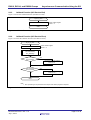
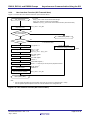
Table 1.1 lists the Peripheral Functions and Their Applications and Figure 1.1 shows a Usage Example.
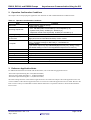
Table 1.1 Peripheral Functions and Their Applications
Peripheral Function
SCI (selectable from 0, 1, 5, 6, 8, 9, and 12)
I/O ports
Application
Asynchronous serial transmission and reception
Turn on LEDs
Renesas Starter Kit for RX210
Terminal software
RX210 Group
Hello world!
RS232C
Computer
TXD
RXD
P14
P15
P16
LED0 output
LED1 output
LED2 output
Figure 1.1 Usage Example
R01AN1423EJ0101 Rev. 1.01
July 1, 2014
Page 3 of 36
RX210, RX21A, and RX220 Groups
Asynchronous Communication Using the SCI
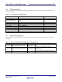
2. Operation Confirmation Conditions
The sample code accompanying this application note has been run and confirmed under the conditions below.
Table 2.1 Operation Confirmation Conditions
Item
MCU used
Operating frequencies
Operating voltage
Integrated development
environment
C compiler
iodefine.h version
Endian
Operating mode
Processor mode
Sample code version
Board used
Tool used
Contents
R5F52108ADFP (RX210 Group)
- Main clock: 20 MHz
- PLL: 100 MHz (main clock divided by 2 and multiplied by 10)
- System clock (ICLK): 50 MHz (PLL divided by 2)
- Peripheral module clock B (PCLKB): 25 MHz (PLL divided by 4)
5.0 V
Renesas Electronics Corporation
High-performance Embedded Workshop Version 4.09.01
Renesas Electronics Corporation
C/C++ Compiler Package for RX Family V.1.02 Release 01
Compile options
-cpu=rx200 -output=obj="$(CONFIGDIR)\$(FILELEAF).obj" -debug -nologo
(The default setting is used in the integrated development environment.)
Version 1.2A
Little endian
Single-chip mode
Supervisor mode
Version 1.00
Renesas Starter Kit for RX210 (product part no.: R0K505210C000BE)
Terminal software
3. Reference Application Notes
For additional information associated with this document, refer to the following application notes.
- RX210 Group Initial Setting Rev. 2.00 (R01AN1002EJ)
- RX21A Group Initial Setting Rev. 1.10 (R01AN1486EJ)
- RX220 Group Initial Setting Rev. 1.10 (R01AN1494EJ)
The initial setting functions in the reference application notes are used in the sample code in this application note. The
revision numbers of the reference application notes are current as of when this application note was made. However the
latest version is always recommended. Visit the Renesas Electronics Corporation website to check and download the
latest version.
R01AN1423EJ0101 Rev. 1.01
July 1, 2014
Page 4 of 36
RX210, RX21A, and RX220 Groups
Asynchronous Communication Using the SCI
4. Hardware
4.1
Pins Used
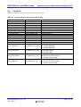
Table 4.1 lists the Pins Used and Their Functions.
The number of pins in the sample code is set for the 100-pin package. When using products with less than 100 pins,
select pins appropriate to the package used.
Table 4.1 Pins Used and Their Functions
Pin Name
I/O
Function
P14
LED0 output (completion of SCI transmission)
Output
P15
LED1 output (completion of SCI reception)
Output
P16
LED2 output (SCI reception error)
Output
P21/RXD0
Input pin for SCI0 receive data (1)
Input
P20/TXD0
Output pin for SCI0 transmit data (1)
Output
P15/RXD1
Input pin for SCI1 receive data (1)
Input
P16/TXD1
Output pin for SCI1 transmit data (1)
Output
PA3/RXD5
Input pin for SCI5 receive data (1)
Input
PA4/TXD5
Output pin for SCI5 transmit data (1)
Output
PB0/RXD6
Input pin for SCI6 receive data (1)
Input
PB1/TXD6
Output pin for SCI6 transmit data (1)
Output
PC6/RXD8
Input pin for SCI8 receive data (1)
Input
PC7/TXD8
Output pin for SCI8 transmit data (1)
Output
PB6/RXD9
Input pin for SCI9 receive data (1)
Input
PB7/TXD9
Output pin for SCI9 transmit data (1)
Output
PE2/RXD12
Input pin for SCI12 receive data (1)
Input
PE1/TXD12
Output pin for SCI12 transmit data (1)
Output
Note:
1. The SCI pins used depend on the SCI channel selected in the configuration file. Unused SCI pins can
be used as general I/O ports.
R01AN1423EJ0101 Rev. 1.01
July 1, 2014
Page 5 of 36
RX210, RX21A, and RX220 Groups
Asynchronous Communication Using the SCI
5. Software
After a reset, the user interface function (SCI initialization) is called to initialize the SCI.
When the user interface function (SCI receive start) is called, receive operation is enabled. When data for the specified
number of bytes have been received, the SCI receive operation is disabled and the callback function (SCI receive end) is
called. LED1 is turned on with the callback function (SCI receive end).
When a receive error occurs, the SCI receive operation is disabled and the callback function (SCI reception error) is
called. LED2 is turned on with the callback function (SCI receive error).
When the user interface function (SCI transmit start) is called, the transmit operation is enabled. When data for the
specified number of bytes have been transmitted, the SCI transmit operation is disabled and the callback function (SCI
transmit end) is called. LED0 is turned on with the callback function (SCI transmit end).
Peripheral function settings are shown below and Figure 5.1 shows the Software Configuration.
SCI
- Serial communication mode: Asynchronous operation
- Transfer rate: 57600 bps
- Clock source: PCLKB (25 MHz)
- Data length: 8 bits
- Stop bit: 2 bits
- Parity: None
- Interrupts: Receive error interrupt (ERI) enabled
Receive data full interrupt (RXI) enabled
Transmit data empty interrupt (TXI) enabled
Transmit end interrupt (TEI) enabled
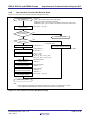
Asynchronous communication (sci.c)
Main processing (main.c)
User interface function
(SCI initialization)
User interface function
(SCI receive start)
Main function
User interface function
(SCI transmit start)
Callback function (SCI transmit end)
User interface function
(SCI state obtain )
Transmit data empty interrupt
function
Callback function (SCI receive end)
Callback function (SCI receive error)
Transmit end interrupt function
Receive data full interrupt function
Receive error interrupt function
External function
(global)
Internal function
(static)
Calls functions
Figure 5.1 Software Configuration
R01AN1423EJ0101 Rev. 1.01
July 1, 2014
Page 6 of 36
RX210, RX21A, and RX220 Groups
5.1
5.1.1
Asynchronous Communication Using the SCI
Operation Overview
Serial Transmission
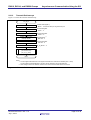
Figure 5.2 shows the Timing of Serial Transmission and (1) to (4) in the figure correspond to numbers in the operation
descriptions below.
(1) Initialization
Initializes the SCI using the user interface function (SCI initialization) and switches the output level on the TXD
pin to high.
(2) Starting a transmission
Verifies the transmit busy flag (B_TX_BUSY) using the user interface function (SCI transmit start). When the flag
is 1 (transmission busy), SCI_BUSY (SCI transmission being processed) is returned. When the flag is 0
(transmission ready), sets the transmit busy flag to 1, the SCR.TIE bit to 1 (a TXI interrupt request is enabled), and
the SCR.TE bit to 1 (serial transmission is enabled). When the TE bit is set to 1, the TXD pin becomes enabled.
Then sets the TXD pin mode control bit to 1 (use pin as I/O port for peripheral functions) to switch the pin function
to TXD output. When the IEN bit for the TXI interrupt is set to 1 (interrupt request is enabled), the TXI interrupt
request is generated.
(3) Transmitting data
In the TXI interrupt handling, the value in the transmit buffer is written to the TDR register. When the last data is
written, sets the TIE bit to 0 (a TXI interrupt request is disabled) and the SCR.TEIE bit to 1 (a TEI interrupt request
is enabled).
(4) Completing the transmission
When the last data has been transmitted, a TEI interrupt request is generated. In the TEI interrupt handling, sets the
TXD pin mode control bit to 0 (use pin as general I/O port), the TE bit to 0 (serial transmission is disabled), and the
TEIE bit to 0 (a TEI interrupt request is disabled). Sets the transmit busy flag to 0 and calls the callback function
(SCI transmit end).
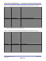
(1)
(4)
1
Transmit busy flag
0
1
SCR.TIE bit
0
1
SCR.TE bit
1
0
Sets to 1 by a program
1
IEN bit for the TXI interrupt
Sets the TXD pin mode
control bit to 0 and then
sets the TE bit to 0
Sets the TE bit to 1 and
then sets the TXD pin
mode control bit to 1
0
SCR.TEIE bit
Sets to 0 by a program
Becomes 0 by an interrupt
acceptance
0
1
IR flag for the TXI interrupt
0
Sets to 0 by a program
1
IEN bit for the TEI interrupt
Sets to 1 by a program
0
1
IR flag for the TEI interrupt
Becomes 0 by an
interrupt acceptance
0
1
TXD pin mode control bit
(PMR register) (1)
TXD pin
(3)
(2)
0
High
Low
General
input port
General
output port
Hi-Z
Note:
1. The bit specified depends on the SCI channel selected.
General
output port
TXD output
H
l
d
!
Transmit data (Hello world!)
Figure 5.2 Timing of Serial Transmission
R01AN1423EJ0101 Rev. 1.01
July 1, 2014
Page 7 of 36
RX210, RX21A, and RX220 Groups
5.1.2
Asynchronous Communication Using the SCI
Serial Reception
Figure 5.3 shows the Timing of Serial Reception and (1) to (4) in the figure correspond to numbers in the operation
descriptions below.
(1) Initialization
Initializes the SCI using the user interface function (SCI initialization) and switches the RXD pin function to RXD
input.
(2) Starting a reception
Verifies the receive busy flag (B_RX_BUSY) using the user interface function (SCI receive start). When the flag is
1 (reception busy), SCI_BUSY (SCI reception being processed) is returned. When the flag is 0 (reception ready),
sets the receive busy flag to 1 and clears the error flags. Sets the SCR.RIE bit to 1 (RXI and ERI interrupt requests
are enabled), the SCR.RE bit to 1 (serial reception is enabled), and the IEN bit for the RXI and ERI interrupts to 1
(interrupt request is enabled).
(3) Receiving data
When data is received, an RXI interrupt request is generated. In the RXI interrupt handling, stores the RDR register
value in the receive buffer.
When a reception error occurs, an ERI interrupt request is generated. In the ERI interrupt handling, sets the error
flag variable and dummy reads the RDR register. Sets the RE bit to 0 and clears the error flags in the SSR register.
Sets the RIE bit to 0, the receive busy flag to 0, and calls the callback function (SCI reception error).
(4) Completing the reception
When the last data has been received, in the RXI interrupt handling, sets the RE bit to 0 (serial reception is
disabled) and RIE bit to 0 (RXI and ERI interrupt requests are disabled). Sets the receive busy flag to 0 and calls
the callback function (SCI receive end).
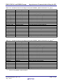
(1)
Reception busy flag
SCR.RIE bit
SCR.RE bit
IEN bit for the RXI interrupt
IR flag for the RXI interrupt
RXD pin mode control bit
(PMR register) (1)
RXD pin
(3)
(2)
(4)
1
0
1
0
1
Sets to 1 by a program
0
Sets to 0 by a program
1
Becomes 0 by an interrupt acceptance
0
1
0
1
0
High
Low
General
input port
Hi-Z
RXD input
Data 0
Data 1
Data 9
Data 10
Data 11
Receive data
Note:
1. The bit specified depends on the SCI channel selected.
Figure 5.3 Timing of Serial Reception
R01AN1423EJ0101 Rev. 1.01
July 1, 2014
Page 8 of 36
RX210, RX21A, and RX220 Groups
5.2
Asynchronous Communication Using the SCI
File Composition
Table 5.1 lists the Files Used in the Sample Code. Files generated by the integrated development environment are not
included in this table.
Table 5.1 Files Used in the Sample Code
File Name
Outline
main.c
r_init_stop_module.c
r_init_stop_module.h
r_init_non_existent_port.c
r_init_non_existent_port.h
r_init_clock.c
r_init_clock.h
sci.c
sci.h
sci_cfg.h
5.3
Remarks
Main processing
Stop processing for active peripheral functions after a
reset
Header file for r_init_stop_module.c
Nonexistent port initialization
Header file for r_init_non_existent_port.c
Clock initialization
Header file for r_init_clock.c
Asynchronous communication
Header file for sci.c
Header file for sci.c configuration file
SCI channel selection
Option-Setting Memory
Table 5.2 lists the Option-Setting Memory Configured in the Sample Code. When necessary, set a value suited to the
user system.
Table 5.2 Option-Setting Memory Configured in the Sample Code
Symbol
Address
Setting Value
OFS0
FFFF FF8Fh to FFFF FF8Ch
FFFF FFFFh
OFS1
FFFF FF8Bh to FFFF FF88h
FFFF FFFFh
MDES
FFFF FF83h to FFFF FF80h
FFFF FFFFh
R01AN1423EJ0101 Rev. 1.01
July 1, 2014
Contents
The IWDT is stopped after a reset.
The WDT is stopped after a reset.
The voltage monitor 0 reset is disabled
after a reset.
HOCO oscillation is disabled after a reset.
Little endian
Page 9 of 36
RX210, RX21A, and RX220 Groups
5.4
Asynchronous Communication Using the SCI
Constants
Table 5.3 to Table 5.12 list the Constants Used in the Sample Code.
Table 5.3 Constants Used in the Sample Code (main.c)
Constant Name
LED0_REG_PODR
LED0_REG_PDR
LED0_REG_PMR
LED1_REG_PODR
LED1_REG_PDR
LED1_REG_PMR
LED2_REG_PODR
LED2_REG_PDR
LED2_REG_PMR
LED_ON
LED_OFF
BUF_SIZE
NULL_SIZE
Setting Value
PORT1.PODR.BIT.B4
PORT1.PDR.BIT.B4
PORT1.PMR.BIT.B4
PORT1.PODR.BIT.B5
PORT1.PDR.BIT.B5
PORT1.PMR.BIT.B5
PORT1.PODR.BIT.B6
PORT1.PDR.BIT.B6
PORT1.PMR.BIT.B6
0
1
12
1
SCI_B_TX_BUSY
sci_state.bit.b_tx_busy
SCI_B_RX_BUSY
sci_state.bit.b_rx_busy
SCI_B_RX_ORER
sci_state.bit.b_rx_orer
SCI_B_RX_FER
sci_state.bit.b_rx_fer
R01AN1423EJ0101 Rev. 1.01
July 1, 2014
Contents
LED0 output data store bit
LED0 I/O select bit
LED0 pin mode control bit
LED1 output data store bit
LED1 I/O select bit
LED1 pin mode control bit
LED2 output data store bit
LED2 I/O select bit
LED2 pin mode control bit
LED output data: Turned on
LED output data: Turned off
Buffer size
NULL code size
Transmit busy flag
0: Transmission ready
1: Transmission busy
Receive busy flag
0: Reception ready
1: Reception busy
Overrun error flag
0: Overrun error not occurred
1: Overrun error occurred
Framing error flag
0: Framing error not occurred
1: Framing error occurred
Page 10 of 36
RX210, RX21A, and RX220 Groups
Asynchronous Communication Using the SCI
Table 5.4 Constants Used in the Sample Code (sci.c)
Constant Name
SSR_ERROR_FLAGS
Setting Value
38h
B_TX_BUSY
state.bit.b_tx_busy
B_RX_BUSY
state.bit.b_rx_busy
B_RX_ORER
state.bit.b_rx_orer
B_RX_FER
state.bit.b_rx_fer
Contents
Bit pattern of an error flag in the SCI.SSR register
Transmit busy flag
0: Transmission ready
1: Transmission busy
Receive busy flag
0: Reception ready
1: Reception busy
Overrun error flag
0: Overrun error not occurred
1: Overrun error occurred
Framing error flag
0: Framing error not occurred
1: Framing error occurred
Table 5.5 Constants Used in the Sample Code (sci.h)
Constant Name
Setting Value
SCI_OK
00h
SCI_BUSY
01h
SCI_NG
02h
R01AN1423EJ0101 Rev. 1.01
July 1, 2014
Contents
Return value of the SCI_StartTransmit and SCI_StartReceive
functions:
SCI transmit/receive start
Return value of the SCI_StartTransmit and SCI_StartReceive
functions:
SCI transmission or reception being processed
Return value of the SCI_StartTransmit and SCI_StartReceive
functions:
Argument error (number of bytes to be transmitted/received is 0)
Page 11 of 36
RX210, RX21A, and RX220 Groups
Asynchronous Communication Using the SCI
Table 5.6 Constants Used in the Sample Code (when SELECT_SCI0 is Selected in sci_cfg.h) (1)
Constant Name
Setting Value
Contents
SCIn
SCI0
SCI channel: SCI0
MSTP_SCIn
MSTP(SCI0)
SCI0 module stop setting bit
IPR_SCIn
IPR(SCI0, )
SCI0 interrupt priority level setting bit
IR_SCIn_ERIn
IR(SCI0,ERI0)
SCI0.ERI0 interrupt status flag
IR_SCIn_RXIn
IR(SCI0,RXI0)
SCI0.RXI0 interrupt status flag
IR_SCIn_TXIn
IR(SCI0,TXI0)
SCI0.TXI0 interrupt status flag
IR_SCIn_TEIn
IR(SCI0,TEI0)
SCI0.TEI0 interrupt status flag
IEN_SCIn_ERIn
IEN(SCI0,ERI0)
SCI0.ERI0 interrupt request enable bit
IEN_SCIn_RXIn
IEN(SCI0,RXI0)
SCI0.RXI0 interrupt request enable bit
IEN_SCIn_TXIn
IEN(SCI0,TXI0)
SCI0.TXI0 interrupt request enable bit
IEN_SCIn_TEIn
IEN(SCI0,TEI0)
SCI0.TEI0 interrupt request enable bit
RXDn_PDR
PORT2.PDR.BIT.B1
P21 I/O select bit
RXDn_PMR
PORT2.PMR.BIT.B1
P21 pin mode control bit
RXDnPFS
P21PFS
P21 pin function control register
TXDn_PODR
PORT2.PODR.BIT.B0
P20 output data store bit
TXDn_PDR
PORT2.PDR.BIT.B0
P20 I/O select bit
TXDn_PMR
PORT2.PMR.BIT.B0
P20 pin mode control bit
TXDnPFS
P20PFS
P20 pin function control register
PSEL_SETTING
0Ah
Setting value of the pin function select bit: RXD0, TXD0
Note:
1. SCI0 is not available in 48-pin and 64-pin products.
Table 5.7 Constants Used in the Sample Code (when SELECT_SCI1 is Selected in sci_cfg.h)
Constant Name
SCIn
MSTP_SCIn
IPR_SCIn
IR_SCIn_ERIn
IR_SCIn_RXIn
IR_SCIn_TXIn
IR_SCIn_TEIn
IEN_SCIn_ERIn
IEN_SCIn_RXIn
IEN_SCIn_TXIn
IEN_SCIn_TEIn
RXDn_PDR
RXDn_PMR
RXDnPFS
TXDn_PODR
TXDn_PDR
TXDn_PMR
TXDnPFS
PSEL_SETTING
Setting Value
SCI1
MSTP(SCI1)
IPR(SCI1, )
IR(SCI1,ERI1)
IR(SCI1,RXI1)
IR(SCI1,TXI1)
IR(SCI1,TEI1)
IEN(SCI1,ERI1)
IEN(SCI1,RXI1)
IEN(SCI1,TXI1)
IEN(SCI1,TEI1)
PORT1.PDR.BIT.B5
PORT1.PMR.BIT.B5
P15PFS
PORT1.PODR.BIT.B6
PORT1.PDR.BIT.B6
PORT1.PMR.BIT.B6
P16PFS
0Ah
R01AN1423EJ0101 Rev. 1.01
July 1, 2014
Contents
SCI channel: SCI1
SCI1 module stop setting bit
SCI1 interrupt priority level setting bit
SCI1.ERI1 interrupt status flag
SCI1.RXI1 interrupt status flag
SCI1.TXI1 interrupt status flag
SCI1.TEI1 interrupt status flag
SCI1.ERI1 interrupt request enable bit
SCI1.RXI1 interrupt request enable bit
SCI1.TXI1 interrupt request enable bit
SCI1.TEI1 interrupt request enable bit
P15 I/O select bit
P15 pin mode control bit
P15 pin function control register
P16 output data store bit
P16 I/O select bit
P16 pin mode control bit
P16 pin function control register
Setting value of the pin function select bit: RXD1, TXD1
Page 12 of 36
RX210, RX21A, and RX220 Groups
Asynchronous Communication Using the SCI
Table 5.8 Constants Used in the Sample Code (when SELECT_SCI5 is Selected in sci_cfg.h)
Constant Name
SCIn
MSTP_SCIn
IPR_SCIn
IR_SCIn_ERIn
IR_SCIn_RXIn
IR_SCIn_TXIn
IR_SCIn_TEIn
IEN_SCIn_ERIn
IEN_SCIn_RXIn
IEN_SCIn_TXIn
IEN_SCIn_TEIn
RXDn_PDR
RXDn_PMR
RXDnPFS
TXDn_PODR
TXDn_PDR
TXDn_PMR
TXDnPFS
PSEL_SETTING
Setting Value
SCI5
MSTP(SCI5)
IPR(SCI5, )
IR(SCI5,ERI5)
IR(SCI5,RXI5)
IR(SCI5,TXI5)
IR(SCI5,TEI5)
IEN(SCI5,ERI5)
IEN(SCI5,RXI5)
IEN(SCI5,TXI5)
IEN(SCI5,TEI5)
PORTA.PDR.BIT.B3
PORTA.PMR.BIT.B3
PA3PFS
PORTA.PODR.BIT.B4
PORTA.PDR.BIT.B4
PORTA.PMR.BIT.B4
PA4PFS
0Ah
Contents
SCI channel: SCI5
SCI5 module stop setting bit
SCI5 interrupt priority level setting bit
SCI5.ERI5 interrupt status flag
SCI5.RXI5 interrupt status flag
SCI5.TXI5 interrupt status flag
SCI5.TEI5 interrupt status flag
SCI5.ERI5 interrupt request enable bit
SCI5.RXI5 interrupt request enable bit
SCI5.TXI5 interrupt request enable bit
SCI5.TEI5 interrupt request enable bit
PA3 I/O select bit
PA3 pin mode control bit
PA3 pin function control register
PA4 output data store bit
PA4 I/O select bit
PA4 pin mode control bit
PA4 pin function control register
Setting value of the pin function select bit: RXD5, TXD5
Table 5.9 Constants Used in the Sample Code (when SELECT_SCI6 is Selected in sci_cfg.h)
Constant Name
SCIn
MSTP_SCIn
IPR_SCIn
IR_SCIn_ERIn
IR_SCIn_RXIn
IR_SCIn_TXIn
IR_SCIn_TEIn
IEN_SCIn_ERIn
IEN_SCIn_RXIn
IEN_SCIn_TXIn
IEN_SCIn_TEIn
RXDn_PDR
RXDn_PMR
RXDnPFS
TXDn_PODR
TXDn_PDR
TXDn_PMR
TXDnPFS
PSEL_SETTING
Setting Value
SCI6
MSTP(SCI6)
IPR(SCI6, )
IR(SCI6,ERI6)
IR(SCI6,RXI6)
IR(SCI6,TXI6)
IR(SCI6,TEI6)
IEN(SCI6,ERI6)
IEN(SCI6,RXI6)
IEN(SCI6,TXI6)
IEN(SCI6,TEI6)
PORTB.PDR.BIT.B0
PORTB.PMR.BIT.B0
PB0PFS
PORTB.PODR.BIT.B1
PORTB.PDR.BIT.B1
PORTB.PMR.BIT.B1
PB1PFS
0Bh
R01AN1423EJ0101 Rev. 1.01
July 1, 2014
Contents
SCI channel: SCI6
SCI6 module stop setting bit
SCI6 interrupt priority level setting bit
SCI6.ERI6 interrupt status flag
SCI6.RXI6 interrupt status flag
SCI6.TXI6 interrupt status flag
SCI6.TEI6 interrupt status flag
SCI6.ERI6 interrupt request enable bit
SCI6.RXI6 interrupt request enable bit
SCI6.TXI6 interrupt request enable bit
SCI6.TEI6 interrupt request enable bit
PB0 I/O select bit
PB0 pin mode control bit
PB0 pin function control register
PB1 output data store bit
PB1 I/O select bit
PB1 pin mode control bit
PB1 pin function control register
Setting value of the pin function select bit: RXD6, TXD6
Page 13 of 36
RX210, RX21A, and RX220 Groups
Asynchronous Communication Using the SCI
Table 5.10 Constants Used in the Sample Code (when SELECT_SCI8 is Selected in sci_cfg.h)
Constant Name
SCIn
MSTP_SCIn
IPR_SCIn
IR_SCIn_ERIn
IR_SCIn_RXIn
IR_SCIn_TXIn
IR_SCIn_TEIn
IEN_SCIn_ERIn
IEN_SCIn_RXIn
IEN_SCIn_TXIn
IEN_SCIn_TEIn
RXDn_PDR
RXDn_PMR
RXDnPFS
TXDn_PODR
TXDn_PDR
TXDn_PMR
TXDnPFS
PSEL_SETTING
Setting Value
SCI8
MSTP(SCI8)
IPR(SCI8, )
IR(SCI8,ERI8)
IR(SCI8,RXI8)
IR(SCI8,TXI8)
IR(SCI8,TEI8)
IEN(SCI8,ERI8)
IEN(SCI8,RXI8)
IEN(SCI8,TXI8)
IEN(SCI8,TEI8)
PORTC.PDR.BIT.B6
PORTC.PMR.BIT.B6
PC6PFS
PORTC.PODR.BIT.B7
PORTC.PDR.BIT.B7
PORTC.PMR.BIT.B7
PC7PFS
0Ah
Contents
SCI channel: SCI8
SCI8 module stop setting bit
SCI8 interrupt priority level setting bit
SCI8.ERI8 interrupt status flag
SCI8.RXI8 interrupt status flag
SCI8.TXI8 interrupt status flag
SCI8.TEI8 interrupt status flag
SCI8.ERI8 interrupt request enable bit
SCI8.RXI8 interrupt request enable bit
SCI8.TXI8 interrupt request enable bit
SCI8.TEI8 interrupt request enable bit
PC6 I/O select bit
PC6 pin mode control bit
PC6 pin function control register
PC7 output data store bit
PC7 I/O select bit
PC7 pin mode control bit
PC7 pin function control register
Setting value of the pin function select bit: RXD8, TXD8
Table 5.11 Constants Used in the Sample Code (when SELECT_SCI9 is Selected in sci_cfg.h) (1)
Constant Name
Setting Value
SCIn
SCI9
MSTP_SCIn
MSTP(SCI9)
IPR_SCIn
IPR(SCI9, )
IR_SCIn_ERIn
IR(SCI9,ERI9)
IR_SCIn_RXIn
IR(SCI9,RXI9)
IR_SCIn_TXIn
IR(SCI9,TXI9)
IR_SCIn_TEIn
IR(SCI9,TEI9)
IEN_SCIn_ERIn
IEN(SCI9,ERI9)
IEN_SCIn_RXIn
IEN(SCI9,RXI9)
IEN_SCIn_TXIn
IEN(SCI9,TXI9)
IEN_SCIn_TEIn
IEN(SCI9,TEI9)
RXDn_PDR
PORTB.PDR.BIT.B6
RXDn_PMR
PORTB.PMR.BIT.B6
RXDnPFS
PB6PFS
TXDn_PODR
PORTB.PODR.BIT.B7
TXDn_PDR
PORTB.PDR.BIT.B7
TXDn_PMR
PORTB.PMR.BIT.B7
TXDnPFS
PB7PFS
PSEL_SETTING
0Ah
Note:
1. SCI9 is not available in 48-pin products.
R01AN1423EJ0101 Rev. 1.01
July 1, 2014
Contents
SCI channel: SCI9
SCI9 module stop setting bit
SCI9 interrupt priority level setting bit
SCI9.ERI9 interrupt status flag
SCI9.RXI9 interrupt status flag
SCI9.TXI9 interrupt status flag
SCI9.TEI9 interrupt status flag
SCI9.ERI9 interrupt request enable bit
SCI9.RXI9 interrupt request enable bit
SCI9.TXI9 interrupt request enable bit
SCI9.TEI9 interrupt request enable bit
PB6 I/O select bit
PB6 pin mode control bit
PB6 pin function control register
PB7 output data store bit
PB7 I/O select bit
PB7 pin mode control bit
PB7 pin function control register
Setting value of the pin function select bit: RXD9, TXD9
Page 14 of 36
RX210, RX21A, and RX220 Groups
Asynchronous Communication Using the SCI
Table 5.12 Constants Used in the Sample Code (when SELECT_SCI12 is Selected in sci_cfg.h)
Constant Name
SCIn
MSTP_SCIn
IPR_SCIn
IR_SCIn_ERIn
IR_SCIn_RXIn
IR_SCIn_TXIn
IR_SCIn_TEIn
IEN_SCIn_ERIn
IEN_SCIn_RXIn
IEN_SCIn_TXIn
IEN_SCIn_TEIn
RXDn_PDR
RXDn_PMR
RXDnPFS
TXDn_PODR
TXDn_PDR
TXDn_PMR
TXDnPFS
PSEL_SETTING
Setting Value
SCI12
MSTP(SCI12)
IPR(SCI12, )
IR(SCI12,ERI12)
IR(SCI12,RXI12)
IR(SCI12,TXI12)
IR(SCI12,TEI12)
IEN(SCI12,ERI12)
IEN(SCI12,RXI12)
IEN(SCI12,TXI12)
IEN(SCI12,TEI12)
PORTE.PDR.BIT.B2
PORTE.PMR.BIT.B2
PE2PFS
PORTE.PODR.BIT.B1
PORTE.PDR.BIT.B1
PORTE.PMR.BIT.B1
PE1PFS
0Ch
R01AN1423EJ0101 Rev. 1.01
July 1, 2014
Contents
SCI channel: SCI12
SCI12 module stop setting bit
SCI12 interrupt priority level setting bit
SCI12.ERI12 interrupt status flag
SCI12.RXI12 interrupt status flag
SCI12.TXI12 interrupt status flag
SCI12.TEI12 interrupt status flag
SCI12.ERI12 interrupt request enable bit
SCI12.RXI12 interrupt request enable bit
SCI12.TXI12 interrupt request enable bit
SCI12.TEI12 interrupt request enable bit
PE2 I/O select bit
PE2 pin mode control bit
PE2 pin function control register
PE1 output data store bit
PE1 I/O select bit
PE1 pin mode control bit
PE1 pin function control register
Setting value of the pin function select bit: RXD12, TXD12
Page 15 of 36
RX210, RX21A, and RX220 Groups
5.5
Asynchronous Communication Using the SCI
Structure/Union List
Figure 5.4 shows the Structure/Union Used in the Sample Code.
#pragma bit_order
left
#pragma unpack
typedef union
{
uint8_t byte;
struct
{
uint8_t b_tx_busy
uint8_t b_rx_busy
uint8_t b_rx_orer
uint8_t b_rx_fer
uint8_t
} bit;
} sci_state_t;
#pragma packoption
#pragma bit_order
/* Bit field order: The bit field members are allocated from upper bits */
/* The boundary alignment value for structure members: Alignment by member type */
:1;
:1;
:1;
:1;
:4;
/* Transmit busy flag
/* Receive busy flag
/* Overrun error flag
/* Framing error flag
/* Not used */
0: Transmission ready
0: Reception ready
0: Overrun error not occurred
0: Framing error not occurred
1: Transmission busy */
1: Reception busy */
1: Overrun error occurred */
1: Framing error occurred */
/* End of specification for the boundary alignment value for structure members */
/* End of specification for the bit field order */
Figure 5.4 Structure/Union Used in the Sample Code
5.6
Variables
Table 5.13 lists the static Variables.
Table 5.13 static Variables
Type
static uint8_t
static uint8_t
static sci_state_t
static const uint8_t *
static uint8_t
static uint8_t *
static uint8_t
Variable Name
rx_buf[BUF_SIZE]
tx_buf[]
sci_state
pbuf_tx
tx_cnt
pbuf_rx
rx_cnt
Contents
Receive buffer
Transmit buffer
SCI state
Pointer to the transmit buffer
Transmit counter
Pointer to the reception buffer
Receive counter
static sci_state_t
state
SCI state
R01AN1423EJ0101 Rev. 1.01
July 1, 2014
Function Used
main
main
cb_sci_rx_error
SCI_StartTransmit
sci_txi_isr
SCI_StartReceive
sci_rxi_isr
SCI_StartReceive
SCI_StartTransmit
SCI_GetState
sci_tei_isr
sci_rxi_isr
sci_eri_isr
Page 16 of 36
RX210, RX21A, and RX220 Groups
5.7
Asynchronous Communication Using the SCI
Functions
Table 5.14 lists the Functions Used in the Sample Code.
Table 5.14 Functions Used in the Sample Code
Function Name
main
port_init
R_INIT_StopModule
R_INIT_NonExistentPort
R_INIT_Clock
peripheral_init
cb_sci_tx_end
cb_sci_rx_end
cb_sci_rx_error
SCI_Init
SCI_StartReceive
SCI_StartTransmit
SCI_GetState
sci_txi_isr
sci_tei_isr
sci_rxi_isr
sci_eri_isr
Excep_SCIn_ERIn
Excep_SCIn_RXIn
Excep_SCIn_TXIn
Excep_SCIn_TEIn
5.8
Outline
Main processing
Port initialization
Stop processing for active peripheral functions after a reset
Nonexistent port initialization
Clock initialization
Peripheral function initialization
Callback function (SCI transmit end)
Callback function (SCI receive end)
Callback function (SCI receive error)
User interface function (SCI initialization)
User interface function (SCI receive start)
User interface function (SCI transmit start)
User interface function (SCI state obtain)
Transmit data empty interrupt
Transmit end interrupt
Receive data full interrupt
Receive error interrupt
SCI.ERI interrupt handling
SCI.RXI interrupt handling
SCI.TXI interrupt handling
SCI.TEI interrupt handling
Function Specifications
The following tables list the sample code function specifications.
main
Outline
Header
Declaration
Description
Arguments
Return Value
Main processing
None
void main(void)
After initialization, starts SCI reception and then starts transmission.
None
None
port_init
Outline
Header
Declaration
Description
Arguments
Return Value
Port initialization
None
static void port_init(void)
Initializes the ports.
None
None
R01AN1423EJ0101 Rev. 1.01
July 1, 2014
Page 17 of 36
RX210, RX21A, and RX220 Groups
R_INIT_StopModule
Outline
Header
Declaration
Description
Arguments
Return Value
Remarks
Asynchronous Communication Using the SCI
Stop processing for active peripheral functions after a reset
r_init_stop_module.h
void R_INIT_StopModule(void)
Configures the setting to enter the module stop state.
None
None
Transition to the module stop state is not performed in the sample code. For details
on this function, refer to the Initial Setting application note for the product used.
R_INIT_NonExistentPort
Nonexistent port initialization
Outline
r_init_non_existent_port.h
Header
void R_INIT_NonExistentPort(void)
Declaration
Initializes port direction registers for ports that do not exist in products with less than
Description
100 pins.
None
Arguments
None
Return Value
The number of pins in the sample code is set for the 100-pin package
Remarks
(PIN_SIZE=100). After this function is called, when writing in byte units to the PDR
registers or PODR registers which have nonexistent ports, set the corresponding bits
for nonexistent ports as follows: set the I/O select bits in the PDR registers to 1 and
set the output data store bits in the PODR registers to 0.
For details on this function, refer to the Initial Setting application note for the product
used.
R_INIT_Clock
Outline
Header
Declaration
Description
Arguments
Return Value
Remarks
peripheral_init
Outline
Header
Declaration
Description
Arguments
Return Value
Clock initialization
r_init_clock.h
void R_INIT_Clock(void)
Initializes the clock.
None
None
The sample code selects processing which uses PLL as the system clock without
using the sub-clock.
For details on this function, refer to the Initial Setting application note for the product
used.
Peripheral function initialization
None
static void peripheral_init (void)
Initializes peripheral functions used.
None
None
R01AN1423EJ0101 Rev. 1.01
July 1, 2014
Page 18 of 36
RX210, RX21A, and RX220 Groups
Asynchronous Communication Using the SCI
cb_sci_tx_end
Outline
Header
Declaration
Description
Arguments
Return Value
Callback function (SCI transmit end)
None
static void cb_sci_tx_end(void)
This function is called when the SCI transmission has been completed.
None
None
cb_sci_rx_end
Outline
Header
Declaration
Description
Arguments
Return Value
Callback function (SCI receive end)
None
static void cb_sci_rx_end(void)
This function is called when the SCI reception has been completed.
None
None
cb_sci_rx_error
Outline
Header
Declaration
Description
Arguments
Return Value
Remarks
Callback function (SCI receive error)
None
static void cb_sci_rx_error(void)
This function is called when the SCI receive error occurs.
None
None
Error processing is not performed in the sample code. Add a program as required.
SCI_Init
Outline
Header
Declaration
Description
Arguments
Return Value
User interface function (SCI initialization)
sci.h
void SCI_Init(void)
Initializes the SCI.
None
None
SCI_StartReceive
Outline
User interface function (SCI receive start)
Header
sci.h
Declaration
uint8_t SCI_StartReceive(uint8_t * pbuf, uint8_t num, CallBackFunc pcb_rx_end,
CallBackFunc pcb_rx_error)
Description
Starts SCI reception.
Arguments
uint8_t * pbuf: Pointer to the receive data storage
uint8_t num: Number of bytes to be received
CallBackFunc pcb_rx_end: Pointer to the callback function (SCI receive end)
CallBackFunc pcb_rx_error: Pointer to the callback function (SCI receive error)
Return Value
SCI_NG: Argument error (number of bytes to be received is 0)
SCI_BUSY: SCI reception being processed
SCI_OK: SCI reception started
R01AN1423EJ0101 Rev. 1.01
July 1, 2014
Page 19 of 36
RX210, RX21A, and RX220 Groups
Asynchronous Communication Using the SCI
SCI_StartTransmit
Outline
User interface function (SCI transmit start)
Header
sci.h
Declaration
uint8_t SCI_StartTransmit(const uint8_t * pbuf, uint8_t num, CallBackFunc
pcb_tx_end)
Description
Starts SCI transmission.
Arguments
const uint8_t * pbuf: Pointer to the transmit data storage
uint8_t num: Number of bytes to be transmitted
CallBackFunc pcb_tx_end: Pointer to the callback function (transmit end)
Return Value
SCI_NG: Argument error (number of bytes to be transmitted is 0)
SCI_BUSY: SCI transmission being processed
SCI_OK: SCI transmission started
SCI_GetState
Outline
Header
Declaration
Description
Arguments
Return Value
sci_txi_isr
Outline
Header
Declaration
Description
Arguments
Return Value
sci_tei_isr
Outline
Header
Declaration
Description
Arguments
Return Value
User interface function (SCI state obtain)
sci.h
sci_state_t SCI_GetState(void)
Returns the SCI state.
None
sci_state_t.bit.b_tx_busy: Transmit busy flag
0: Transmission ready
1: Transmission busy
sci_state_t.bit.b_rx_busy: Receive busy flag
0: Reception ready
1: Reception busy
sci_state_t.bit.b_rx_orer: Overrun error flag
0: Overrun error not occurred
1: Overrun error occurred
sci_state_t.bit.b_rx_fer: Framing error flag
0: Framing error not occurred
1: Framing error occurred
Transmit data empty interrupt
None
static void sci_txi_isr(void)
This function is called in the SCI.TXI interrupt handling. Writes the transmit data.
After transmitting the last data, disables the TXI interrupt request and enables TEI
interrupt request.
None
None
Transmit end interrupt
None
static void sci_tei_isr(void)
This function is called in the SCI.TEI interrupt handling. Disables the serial
transmission and calls the callback function (SCI transmit end).
None
None
R01AN1423EJ0101 Rev. 1.01
July 1, 2014
Page 20 of 36
RX210, RX21A, and RX220 Groups
sci_rxi_isr
Outline
Header
Declaration
Description
Arguments
Return Value
sci_eri_isr
Outline
Header
Declaration
Description
Asynchronous Communication Using the SCI
Receive data full interrupt
None
static void sci_rxi_isr(void)
This function is called in the SCI.RXI interrupt handling. Stores the receive data. After
receiving the last data, disables the serial reception and calls the callback function
(SCI receive end).
None
None
Arguments
Return Value
Receive error interrupt
None
static void sci_eri_isr(void)
This function is called in the SCI.ERI interrupt handling. Disables the serial reception
and calls the callback function (SCI receive error).
None
None
Excep_SCIn_ERIn
Outline
Header
Declaration
Description
Arguments
Return Value
SCI.ERI interrupt handling
None
static void Excep_SCIn_ERIn(void)
Performs processing for the receive error interrupt.
None
None
Excep_SCIn_RXIn
Outline
Header
Declaration
Description
Arguments
Return Value
SCI.RXI interrupt handling
None
static void Excep_SCIn_RXIn(void)
Performs processing for the reception data full interrupt.
None
None
Excep_SCIn_TXIn
Outline
Header
Declaration
Description
Arguments
Return Value
SCI.TXI interrupt handling
None
static void Excep_SCIn_TXIn(void)
Performs processing for the transmit data empty interrupt.
None
None
Excep_SCIn_TEIn
Outline
Header
Declaration
Description
Arguments
Return Value
SCI.TEI interrupt handling
None
static void Excep_SCIn_TEIn(void)
Performs processing for the transmit end interrupt.
None
None
R01AN1423EJ0101 Rev. 1.01
July 1, 2014
Page 21 of 36
RX210, RX21A, and RX220 Groups
5.9
5.9.1
Asynchronous Communication Using the SCI
Flowcharts
Main Processing
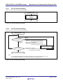
Figure 5.5 shows the Main Processing.
main
Disable maskable interrupts
I flag ← 0
Port initialization
port_init()
Stop processing for active
peripheral functions after a reset
R_INIT_StopModule()
Nonexistent port initialization
R_INIT_NonExistentPort()
Clock initialization
R_INIT_Clock()
Peripheral function initialization
peripheral_init()
Enable maskable interrupts
Initialize the RAM
I flag ← 1
Sets 00h to the receive buffer
User interface function
(SCI receive start)
SCI_StartReceive()
Has SCI reception
started?
SCI reception being processed
SCI reception started or an argument error occurred
User interface function
(SCI transmit start)
SCI_StartTransmit()
Has SCI
transmission started?
SCI transmission being processed
SCI transmission started or an argument error occurred
Figure 5.5 Main Processing
R01AN1423EJ0101 Rev. 1.01
July 1, 2014
Page 22 of 36
RX210, RX21A, and RX220 Groups
5.9.2
Asynchronous Communication Using the SCI
Port Initialization
Figure 5.6 shows the Port Initialization.
port_init
PORT1.PODR register
B4 bit ← 1: LED0: Turned off
B5 bit ← 1: LED1: Turned off
B6 bit ← 1: LED2: Turned off
Set port output data
PORT1.PDR register
B4 bit ← 1: LED0: Output
B5 bit ← 1: LED1: Output
B6 bit ← 1: LED2: Output
Set port directions
PORT1.PMR register
B4 bit ← 0: LED0: Uses pin as general I/O port.
B5 bit ← 0: LED1: Uses pin as general I/O port.
B6 bit ← 0: LED2: Uses pin as general I/O port.
Set port modes
return
Figure 5.6 Port Initialization
5.9.3
Peripheral Function Initialization
Figure 5.7 shows the Peripheral Function Initialization.
peripheral_init
User interface function
(SCI initialization)
SCI_Init()
return
Figure 5.7 Peripheral Function Initialization
5.9.4
Callback Function (SCI Transmit End)
Figure 5.8 shows the Callback Function (SCI Transmit End).
cb_sci_tx_end
Turn on LED0
PORT1.PODR register
B4 bit ← 0
return
Figure 5.8 Callback Function (SCI Transmit End)
R01AN1423EJ0101 Rev. 1.01
July 1, 2014
Page 23 of 36
RX210, RX21A, and RX220 Groups
5.9.5
Asynchronous Communication Using the SCI
Callback Function (SCI Receive End)
Figure 5.9 shows the Callback Function (SCI Receive End).
cb_sci_rx_end
PORT1.PODR register
B5 bit ← 0
Turn on LED1
return
Figure 5.9 Callback Function (SCI Receive End)
5.9.6
Callback Function (SCI Receive Error)
Figure 5.10 shows the Callback Function (SCI Receive Error).
cb_sci_rx_error
Turn on LED2
PORT1.PODR register
B6 bit ← 0
User interface function
(SCI state obtain)
SCI_GetState()
Has an overrun
error occurred?
Yes
Processing when an overrun
error occurs (1)
No
Has a framing
error occurred?
Yes
No
Processing when a framing
error occurs (1)
return
Note:
1. Error processing is not performed in the sample code. Add a program as required.
Figure 5.10 Callback Function (SCI Receive Error)
R01AN1423EJ0101 Rev. 1.01
July 1, 2014
Page 24 of 36
RX210, RX21A, and RX220 Groups
5.9.7
Asynchronous Communication Using the SCI
User Interface Function (SCI Initialization)
Figure 5.11 and Figure 5.12 show the User Interface Function (SCI Initialization).
SCI_Init
Disable the SCIn interrupt request
Cancel the module stop state
Disable transmission/reception and
disable interrupt requests (3)
Set the port output data
Set port directions
Set port modes
IER1A register (1)
IEN6 bit ← 0: SCI0.ERI0 interrupt request is disabled.
IEN7 bit ← 0: SCI0.RXI0 interrupt request is disabled.
IER1B register (1)
IEN0 bit ← 0: SCI0.TXI0 interrupt request is disabled.
IEN1 bit ← 0: SCI0.TEI0 interrupt request is disabled.
PRCR register ← A502h
PRC1 bit = 1: Enables writing to registers related to the operation.
MSTPCRB register (1)
MSTPB31 bit ← 0: The module stop state is canceled for the SCI0 module.
PRCR register ← A500h
PRC1 bit = 0: Disables writing to registers related to the operation.
SCIn.SCR register ← 00h
TEIE bit = 0: A TEI interrupt request is disabled.
RE bit = 0: Serial reception is disabled.
TE bit = 0: Serial transmission is disabled.
RIE bit = 0: RXI and ERI interrupt requests are disabled.
TIE bit = 0: A TXI interrupt request is disabled.
PORT2.PODR register (1)
B0 bit ← 1: TXD0: High level
PORT2.PDR register (1)
B0 bit ← 1: TXD0: Output
B1 bit ← 0: RXD0: Input
PORT2.PMR register (1)
B0 bit ← 0: Uses the TXD0 pin as general I/O port.
B1 bit ← 0: Uses the RXD0 pin as general I/O port.
Enable writing to the PFSWE bit
MPC.PWPR register
B0WI bit ← 0
Enable writing to the PFS register
MPC.PWPR register
PFSWE bit ← 1
Select pin functions
MPC.P20PFS register ← 0Ah (1, 2)
PSEL[3:0] bits = 1010b: TXD0
MPC.P21PFS register ← 0Ah (1, 2)
PSEL[3:0] bits = 1010b: RXD0
Disable writing to the PFS register
MPC.PWPR register
PFSWE bit ← 0
Disable writing to the PFSWE bit
MPC.PWPR register
B0WI bit ← 1
Set the port mode
PORT2.PMR register (1)
B1 bit ← 1: Uses the pin as I/O port for peripheral function.
A
Notes:
1. The I/O register described here is the register used when SCI channel 0 is selected (SCIn = SCI0).
The I/O registers specified depend on the SCI channel selected in the configuration file.
2. The setting value described here is the value when SCI channel 0 is selected.
The setting values specified depend on the SCI channel selected in the configuration file.
3. After writing values to bits RE, TE, RIE and TIE, read these bits to confirm that the written values can be read.
Figure 5.11 User Interface Function (SCI Initialization) (1/2)
R01AN1423EJ0101 Rev. 1.01
July 1, 2014
Page 25 of 36
RX210, RX21A, and RX220 Groups
Asynchronous Communication Using the SCI
A
Select the clock
Set the transmit/receive format
SCIn.SCR register
CKE[1:0] bits ← 00b: On-chip baud rate generator
SCIn.SMR register ← 08h
CKS[1:0] bits = 00b: PCLK clock
MP bit = 0: Multi-processor communications function is disabled.
STOP bit = 1: 2 stop bits
PE bit = 0: Parity bit addition is not performed.
CHR bit = 0: Selects 8 bits as the data length.
CM bit = 0: Asynchronous mode
SCIn.SCMR register ← F2h
SMIF bit = 0: Serial communications interface mode
SINV bit = 0: TDR contents are transmitted as they are.
Receive data is stored as it is in RDR.
SDIR bit = 0: Transfer with LSB-first
SCIn.SEMR register ← 00h
ABCS bit = 0: Selects 16 base clock cycles for 1-bit period.
NFEN bit = 0: Noise cancellation function for the RXDn input signal is disabled.
Set the bit rate
Set the SCIn interrupt priority level
Clear the SCIn interrupt request
-1
SCIn.BRR register ← 13: (25 MHz ÷ (64 × 2 × 57600 bps)) - 1 = 12.56
IPR214 register (1)
IPR[3:0] bits ← 0001b: Level 1
IR215 register (1)
IR flag ← 0: No SCI0.RXI0 interrupt request is generated.
IR216 register (1)
IR flag ← 0: No SCI0.TXI0 interrupt request is generated.
return
Note:
1. The I/O register described here is the register used when SCI channel 0 is selected (SCIn = SCI0).
The I/O registers specified depend on the SCI channel selected in the configuration file.
Figure 5.12 User Interface Function (SCI Initialization) (2/2)
R01AN1423EJ0101 Rev. 1.01
July 1, 2014
Page 26 of 36
RX210, RX21A, and RX220 Groups
5.9.8
Asynchronous Communication Using the SCI
User Interface Function (SCI Receive Start)
Figure 5.13 shows the User Interface Function (SCI Receive Start).
SCI_StartReceive
Set the return value
(argument error)
Is the number of bytes
to be received 0?
Arguments
uint8_t * pbuf: Pointer to the receive data storage
uint8_t num: Number of bytes to be received
CallBackFunc pcb_rx_end: Pointer to the callback function (SCI receive end)
CallBackFunc pcb_rx_error: Pointer to the callback function (SCI receive error)
return_value ← SCI_NG
Yes
No
Is the reception
status busy?
No
return (return_value)
Yes
Reads B_RX_BUSY: 0: Reception ready
: 1: Reception busy
Set the receive busy flag
B_RX_BUSY ← 1
Clear the receive error flags
B_RX_ORER ← 0
B_RX_FER ← 0
Set the arguments to the RAM
SCIn.SCR register
RIE bit ← 1
Enable serial reception
SCIn.SCR register
RE bit ← 1
Set the return value
(SCI reception started)
return_value ← SCI_BUSY
pbuf_rx ← pbuf
rx_cnt ← num
pcb_sci_rx_end ← pcb_rx_end
pcb_sci_rx_error ← pcb_rx_error
Enable RXI and ERI
interrupt requests
Enable SCIn.RXIn and
SCIn.ERIn interrupt requests
Set the return value
(SCI reception being processed)
IER1A register (1)
IEN6 bit ← 1
IEN7 bit ← 1
return_value ← SCI_OK
return (return_value)
Note:
1. The I/O register described here is the register used when SCI channel 0 is selected (SCIn = SCI0).
The I/O register specified depends on the SCI channel selected in the configuration file.
Figure 5.13 User Interface Function (SCI Receive Start)
R01AN1423EJ0101 Rev. 1.01
July 1, 2014
Page 27 of 36
RX210, RX21A, and RX220 Groups
5.9.9
Asynchronous Communication Using the SCI
User Interface Function (SCI Transmit Start)
Figure 5.14 shows the User Interface Function (SCI Transmit Start).
Arguments
uint8_t * pbuf: Pointer to the transmit data storage
uint8_t num: Number of bytes to be transmitted
CallBackFunc pcb_tx_end: Pointer to the callback function (SCI transmit end)
SCI_StartTransmit
Set the return value
(argument error)
Is the number of bytes
to be transmitted 0?
return_value ← SCI_NG
Yes
No
Is the transmission
status busy?
No
Set the transmit busy flag
Set the arguments to the RAM
return (return_value)
Yes
Reads B_TX_BUSY: 0: Transmission ready
: 1: Transmission busy
B_TX_BUSY ← 1
pbuf_tx ← pbuf
tx_cnt ← num
pcb_sci_tx_end ← pcb_tx_end
Enable the TXI interrupt request
SCIn.SCR register
TIE bit ← 1
Enable serial transmission
SCIn.SCR register
TE bit ← 1
Set the port mode
Enable the SCIn.TXIn
interrupt request
Set the return value
(SCI transmission started)
Set the return value
(SCI transmission being processed)
return_value ← SCI_BUSY
PORT2.PMR register (1)
B0 bit ← 1: Uses the pin as I/O port for peripheral function.
IER1B register (1)
IEN0 bit ← 1
return_value ← SCI_OK
return (return_value)
Note:
1. The I/O register described here is the register used when SCI channel 0 is selected (SCIn = SCI0).
The I/O registers specified depend on the SCI channel selected in the configuration file.
Figure 5.14 User Interface Function (SCI Transmit Start)
R01AN1423EJ0101 Rev. 1.01
July 1, 2014
Page 28 of 36
RX210, RX21A, and RX220 Groups
5.9.10
Asynchronous Communication Using the SCI
User Interface Function (SCI State Obtain)
Figure 5.15 shows the User Interface Function (SCI State Obtain).
SCI_GetState
Set the SCI state as the return value
return (state)
Figure 5.15 User Interface Function (SCI State Obtain)
5.9.11
Transmit Data Empty Interrupt
Figure 5.16 shows the Transmit Data Empty Interrupt.
sci_txi_isr
Set the transmit data
Dummy read the SSR register
Pointer to the transmit buffer + 1
Transmit counter - 1
No
Is the data
transmitted
the last data?
SCIn.TDR register ← *pbuf_tx
Reads the SCIn.SSR register and performs calculations.
pbuf_tx ← pbuf_tx + 1
tx_cnt ← tx_cnt - 1
Reads tx_cnt.
Yes
Disable the SCIn.TXIn
interrupt request
Disable the TXI interrupt request (2)
Clear the SCIn.TXIn
interrupt request
Enable the TEI interrupt request
Enable the SCIn.TEIn
interrupt request
IER1B register (1)
IEN0 bit ← 0
SCIn.SCR register
TIE bit ← 0
IR216 register (1)
IR flag ← 0
SCIn.SCR register
TEIE bit ← 1
IER1B register (1)
IEN1 bit ← 1
return
Notes:
1. The I/O register described here is the register used when SCI channel 0 is selected (SCIn = SCI0).
The I/O registers specified depend on the SCI channel selected in the configuration file.
2. After writing a value to the TIE bit, read the bit to confirm that the written value can be read.
Figure 5.16 Transmit Data Empty Interrupt
R01AN1423EJ0101 Rev. 1.01
July 1, 2014
Page 29 of 36
RX210, RX21A, and RX220 Groups
5.9.12
Asynchronous Communication Using the SCI
Transmit End Interrupt
Figure 5.17 shows the Transmit End Interrupt.
sci_tei_isr
Set the port mode
PORT2.PMR register (1)
B0 bit ← 0: Uses the TXD0 pin as general I/O port.
Disable serial transmission
SCIn.SCR register
TE bit ← 0
Disable the TXI interrupt request
SCIn.SCR register
TIE bit ← 0
Disable the SCIn.TEIn
interrupt request
IER1B register (1)
IEN1 bit ← 0
Disable the TEI interrupt request (2)
SCIn.SCR register
TEIE bit ← 0
Clear the transmit busy flag
B_TX_BUSY ← 0
Callback function
(SCI transmit end)
pcb_sci_tx_end()
return
Notes:
1. The I/O register described here is the register used when SCI channel 0 is selected (SCIn = SCI0).
The I/O registers specified depend on the SCI channel selected in the configuration file.
2. After writing a value to the TEIE bit, read the bit to confirm that the written value can be read.
Figure 5.17 Transmit End Interrupt
R01AN1423EJ0101 Rev. 1.01
July 1, 2014
Page 30 of 36
RX210, RX21A, and RX220 Groups
5.9.13
Asynchronous Communication Using the SCI
Receive Data Full Interrupt
Figure 5.18 shows the Receive Data Full Interrupt.
sci_rxi_isr
Store the receive data
Pointer to the receive buffer + 1
Receive counter - 1
No
Has the last data
been received?
Yes
Disable serial reception (2)
Disable SCIn.RXIn and
SCIn.ERIn interrupt requests
Disable the RXI and ERI interrupt
requests (2)
Clear the SCIn.RXIn
interrupt request
Clear the receive busy flag
*pbuf_rx ← SCIn.RDR register
pbuf_rx ← pbuf_rx + 1
rx_cnt ← rx_cnt - 1
Reads rx_cnt.
SCIn.SCR register
RE bit ← 0
IER1A register (1)
IEN6 bit ← 0
IEN7 bit ← 0
SCIn.SCR register
RIE bit ← 0
IR215 register (1)
IR flag ← 0
B_RX_BUSY ← 0
Callback function
(SCI receive end)
pcb_sci_rx_end()
return
Notes:
1. The I/O register described here is the register used when SCI channel 0 is selected (SCIn = SCI0).
The I/O registers specified depend on the SCI channel selected in the configuration file.
2. After writing values to bits RE and RIE, read these bits to confirm that the written values can be read.
Figure 5.18 Receive Data Full Interrupt
R01AN1423EJ0101 Rev. 1.01
July 1, 2014
Page 31 of 36
RX210, RX21A, and RX220 Groups
5.9.14
Asynchronous Communication Using the SCI
Receive Error Interrupt
Figure 5.19 shows the Receive Error Interrupt.
sci_eri_isr
No
Has an overrun
error occurred?
Yes
Set the overrun error flag
No
Has a framing
error occurred?
Yes
Set the framing error flag
Dummy read the RDR register
Disable serial reception (2)
Clear error flags (2)
Disable the SCIn.RXIn and
SCIn.ERIn interrupt requests
Disable the RXI and ERI
interrupt requests (2)
Clear the SCIn.RXIn
interrupt request
Clear the receive busy flag
Reads the SCIn.SSR register.
ORER flag: 0: No overrun error occurred
1: An overrun error occurred
B_RX_ORER ← 1
Reads the SCIn.SSR register.
FER flag: 0: No framing error occurred
1: A framing error occurred
B_RX_FER ← 1
Reads the SCIn.RDR register.
SCIn.SCR register
RE bit ← 0
SCIn.SSR register ← (SCIn.SSR register & C7h) | C0h
PER flag = 0: No parity error occurred
FER flag = 0: No framing error occurred
ORER flag = 0: No overrun error occurred
IER1A register (1)
IEN6 bit ← 0
IEN7 bit ← 0
SCIn.SCR register
RIE bit ← 0
IR215 register (1)
IR flag ← 0
B_RX_BUSY ← 0
Callback function
(SCI receive error)
pcb_sci_rx_error()
return
Notes:
1. The I/O register described here is the register used when SCI channel 0 is selected (SCIn = SCI0).
The I/O registers specified depend on the SCI channel selected in the configuration file.
2. After writing values to bits RE and RIE, and flags PER, FER and ORER, read these bits and flags to
confirm that the written values can be read.
Figure 5.19 Receive Error Interrupt
R01AN1423EJ0101 Rev. 1.01
July 1, 2014
Page 32 of 36
RX210, RX21A, and RX220 Groups
5.9.15
Asynchronous Communication Using the SCI
SCI.ERI Interrupt Handling
Figure 5.20 shows the SCI.ERI Interrupt Handling.
Excep_SCIn_ERIn
Determine
the interrupt request
source
Interrupt not
requested
IR = 1
Verify the IR flag
IR = 0
Interrupt
requested
Reads the SCIn.SCR register
RIE bit: 0: RXI and ERI interrupt requests are disabled.
1: RXI and ERI interrupt requests are enabled.
Reads the SCIn.SSR register
PER flag: 0: No parity error occurred
1: A parity error has occurred
FER flag: 0: No framing error occurred
1: A framing error has occurred
ORER flag: 0: No overrun error occurred
1: An overrun error has occurred
Reads the IR214 register (1)
IR flag: 0: No interrupt request is generated.
1: Interrupt request is generated.
Receive error interrupt
sci_eri_isr()
return
Note:
1. The I/O register described here is the register used when SCI channel 0 is selected (SCIn = SCI0).
The I/O register read depends on the SCI channel selected in the configuration file.
Figure 5.20 SCI.ERI Interrupt Handling
5.9.16
SCI.RXI Interrupt Handling
Figure 5.21 shows the SCI.RXI Interrupt Handling.
Excep_SCIn_RXIn
Receive data full interrupt
sci_rxi_isr()
return
Figure 5.21 SCI.RXI Interrupt Handling
R01AN1423EJ0101 Rev. 1.01
July 1, 2014
Page 33 of 36
RX210, RX21A, and RX220 Groups
5.9.17
Asynchronous Communication Using the SCI
SCI.TXI Interrupt Handling
Figure 5.22 shows the SCI.TXI Interrupt Handling.
Excep_SCIn_TXIn
Transmit data empty
interrupt
sci_txi_isr()
return
Figure 5.22 SCI.TXI Interrupt Handling
5.9.18
SCI.TEI Interrupt Handling
Figure 5.23 shows the SCI.TEI Interrupt Handling.
Excep_SCIn_TEIn
Determine
the interrupt request
source
Interrupt
requested
Interrupt not
requested
IR = 1
Verify the IR flag
IR = 0
Reads the SCIn.SCR register
TEIE bit: 0: A TEI interrupt request is disabled.
1: A TEI interrupt request is enabled.
Reads the SCIn.SSR register
TEND flag: 0: A character is being transmitted.
1: Character transfer has been completed.
Reads the IR217 register (1)
IR flag: 0: No interrupt request is generated.
1: Interrupt request is generated.
Transmit end interrupt
sci_tei_isr()
return
Note:
1. The I/O register described here is the register used when SCI channel 0 is selected (SCIn = SCI0).
The I/O register read depends on the SCI channel selected in the configuration file.
Figure 5.23 SCI.TEI Interrupt Handling
R01AN1423EJ0101 Rev. 1.01
July 1, 2014
Page 34 of 36
RX210, RX21A, and RX220 Groups
Asynchronous Communication Using the SCI
6. Applying This Application Note to the RX21A or RX220 Group
The sample code accompanying this application note has been confirmed to operate with the RX210 Group. To make
the sample code operate with the RX21A or RX220 Group, use this application note in conjunction with the Initial
Setting application note for each group.
For details on using this application note with the RX21A and RX220 Groups, refer to “5. Applying the RX210 Group
Application Note to the RX21A Group” in the RX21A Group Initial Setting application note, and “4. Applying the
RX210 Group Application Note to the RX220 Group” in the RX220 Group Initial Setting application note.
Note: • When using the RX21A Group, SCI0 and SCI12 are not available. Use SCI1, SCI5, SCI6, SCI8, or
SCI9.
When using the RX220 Group, SCI0, SCI8, and SCI12 are not available. Use SCI1, SCI5, SCI6, or
SCI9.
R01AN1423EJ0101 Rev. 1.01
July 1, 2014
Page 35 of 36
RX210, RX21A, and RX220 Groups
Asynchronous Communication Using the SCI
7. Sample Code
Sample code can be downloaded from the Renesas Electronics website.
8. Reference Documents
User’s Manual: Hardware
RX210 Group User's Manual: Hardware Rev.1.50 (R01UH0037EJ)
RX21A Group User's Manual: Hardware Rev.1.00 (R01UH0251EJ)
RX220 Group User's Manual: Hardware Rev.1.10 (R01UH0292EJ)
The latest versions can be downloaded from the Renesas Electronics website.
Technical Update/Technical News
The latest information can be downloaded from the Renesas Electronics website.
User’s Manual: Development Tools
RX Family C/C++ Compiler Package V.1.01 User’s Manual Rev.1.00 (R20UT0570EJ)
The latest version can be downloaded from the Renesas Electronics website.
Website and Support
Renesas Electronics website
http://www.renesas.com
Inquiries
http://www.renesas.com/contact/
R01AN1423EJ0101 Rev. 1.01
July 1, 2014
Page 36 of 36
RX210, RX21A, and RX220 Groups Application Note
Asynchronous Communication Using the SCI
REVISION HISTORY
Rev.
Date
1.00
1.01
July 1, 2013
July 1, 2014
Page
—
1
4
18
35
36
Description
Summary
First edition issued
Products: Added the RX21A and RX220 Groups.
3. Reference Application Notes: Added the Initial Setting application
notes for the RX21A and RX220 Groups.
Modified the description of reference application note in the
following functions: R_INIT_StopModule, R_INIT_NonExistentPort,
and R_INIT_Clock.
6. Applying This Application Note to the RX21A or RX220 Group:
Added.
8. Reference Documents: Added the User’s Manual: Hardware for
the RX21A and RX220 Groups.
All trademarks and registered trademarks are the property of their respective owners.
A-1
General Precautions in the Handling of MPU/MCU Products
The following usage notes are applicable to all MPU/MCU products from Renesas. For detailed usage notes on the
products covered by this document, refer to the relevant sections of the document as well as any technical updates that
have been issued for the products.
1. Handling of Unused Pins
Handle unused pins in accordance with the directions given under Handling of Unused Pins in the
manual.
The input pins of CMOS products are generally in the high-impedance state. In operation with an
unused pin in the open-circuit state, extra electromagnetic noise is induced in the vicinity of LSI, an
associated shoot-through current flows internally, and malfunctions occur due to the false
recognition of the pin state as an input signal become possible. Unused pins should be handled as
described under Handling of Unused Pins in the manual.
2. Processing at Power-on
The state of the product is undefined at the moment when power is supplied.
The states of internal circuits in the LSI are indeterminate and the states of register settings and
pins are undefined at the moment when power is supplied.
In a finished product where the reset signal is applied to the external reset pin, the states of pins
are not guaranteed from the moment when power is supplied until the reset process is completed.
In a similar way, the states of pins in a product that is reset by an on-chip power-on reset function
are not guaranteed from the moment when power is supplied until the power reaches the level at
which resetting has been specified.
3. Prohibition of Access to Reserved Addresses
Access to reserved addresses is prohibited.
The reserved addresses are provided for the possible future expansion of functions. Do not access
these addresses; the correct operation of LSI is not guaranteed if they are accessed.
4. Clock Signals
After applying a reset, only release the reset line after the operating clock signal has become stable.
When switching the clock signal during program execution, wait until the target clock signal has
stabilized.
When the clock signal is generated with an external resonator (or from an external oscillator)
during a reset, ensure that the reset line is only released after full stabilization of the clock signal.
Moreover, when switching to a clock signal produced with an external resonator (or by an external
oscillator) while program execution is in progress, wait until the target clock signal is stable.
5. Differences between Products
Before changing from one product to another, i.e. to a product with a different part number, confirm
that the change will not lead to problems.
The characteristics of an MPU or MCU in the same group but having a different part number may
differ in terms of the internal memory capacity, layout pattern, and other factors, which can affect
the ranges of electrical characteristics, such as characteristic values, operating margins, immunity
to noise, and amount of radiated noise. When changing to a product with a different part number,
implement a system-evaluation test for the given product.
Notice
1.
Descriptions of circuits, software and other related information in this document are provided only to illustrate the operation of semiconductor products and application examples. You are fully responsible for
the incorporation of these circuits, software, and information in the design of your equipment. Renesas Electronics assumes no responsibility for any losses incurred by you or third parties arising from the
use of these circuits, software, or information.
2.
Renesas Electronics has used reasonable care in preparing the information included in this document, but Renesas Electronics does not warrant that such information is error free. Renesas Electronics
assumes no liability whatsoever for any damages incurred by you resulting from errors in or omissions from the information included herein.
3.
Renesas Electronics does not assume any liability for infringement of patents, copyrights, or other intellectual property rights of third parties by or arising from the use of Renesas Electronics products or
technical information described in this document. No license, express, implied or otherwise, is granted hereby under any patents, copyrights or other intellectual property rights of Renesas Electronics or
others.
4.
You should not alter, modify, copy, or otherwise misappropriate any Renesas Electronics product, whether in whole or in part. Renesas Electronics assumes no responsibility for any losses incurred by you or
third parties arising from such alteration, modification, copy or otherwise misappropriation of Renesas Electronics product.
5.
Renesas Electronics products are classified according to the following two quality grades: "Standard" and "High Quality". The recommended applications for each Renesas Electronics product depends on
the product's quality grade, as indicated below.
"Standard": Computers; office equipment; communications equipment; test and measurement equipment; audio and visual equipment; home electronic appliances; machine tools; personal electronic
equipment; and industrial robots etc.
"High Quality": Transportation equipment (automobiles, trains, ships, etc.); traffic control systems; anti-disaster systems; anti-crime systems; and safety equipment etc.
Renesas Electronics products are neither intended nor authorized for use in products or systems that may pose a direct threat to human life or bodily injury (artificial life support devices or systems, surgical
implantations etc.), or may cause serious property damages (nuclear reactor control systems, military equipment etc.). You must check the quality grade of each Renesas Electronics product before using it
in a particular application. You may not use any Renesas Electronics product for any application for which it is not intended. Renesas Electronics shall not be in any way liable for any damages or losses
incurred by you or third parties arising from the use of any Renesas Electronics product for which the product is not intended by Renesas Electronics.
6.
You should use the Renesas Electronics products described in this document within the range specified by Renesas Electronics, especially with respect to the maximum rating, operating supply voltage
range, movement power voltage range, heat radiation characteristics, installation and other product characteristics. Renesas Electronics shall have no liability for malfunctions or damages arising out of the
use of Renesas Electronics products beyond such specified ranges.
7.
Although Renesas Electronics endeavors to improve the quality and reliability of its products, semiconductor products have specific characteristics such as the occurrence of failure at a certain rate and
malfunctions under certain use conditions. Further, Renesas Electronics products are not subject to radiation resistance design. Please be sure to implement safety measures to guard them against the
possibility of physical injury, and injury or damage caused by fire in the event of the failure of a Renesas Electronics product, such as safety design for hardware and software including but not limited to
redundancy, fire control and malfunction prevention, appropriate treatment for aging degradation or any other appropriate measures. Because the evaluation of microcomputer software alone is very difficult,
please evaluate the safety of the final products or systems manufactured by you.
8.
Please contact a Renesas Electronics sales office for details as to environmental matters such as the environmental compatibility of each Renesas Electronics product. Please use Renesas Electronics
products in compliance with all applicable laws and regulations that regulate the inclusion or use of controlled substances, including without limitation, the EU RoHS Directive. Renesas Electronics assumes
no liability for damages or losses occurring as a result of your noncompliance with applicable laws and regulations.
9.
Renesas Electronics products and technology may not be used for or incorporated into any products or systems whose manufacture, use, or sale is prohibited under any applicable domestic or foreign laws or
regulations. You should not use Renesas Electronics products or technology described in this document for any purpose relating to military applications or use by the military, including but not limited to the
development of weapons of mass destruction. When exporting the Renesas Electronics products or technology described in this document, you should comply with the applicable export control laws and
regulations and follow the procedures required by such laws and regulations.
10. It is the responsibility of the buyer or distributor of Renesas Electronics products, who distributes, disposes of, or otherwise places the product with a third party, to notify such third party in advance of the
contents and conditions set forth in this document, Renesas Electronics assumes no responsibility for any losses incurred by you or third parties as a result of unauthorized use of Renesas Electronics
products.
11. This document may not be reproduced or duplicated in any form, in whole or in part, without prior written consent of Renesas Electronics.
12. Please contact a Renesas Electronics sales office if you have any questions regarding the information contained in this document or Renesas Electronics products, or if you have any other inquiries.
(Note 1)
"Renesas Electronics" as used in this document means Renesas Electronics Corporation and also includes its majority-owned subsidiaries.
(Note 2)
"Renesas Electronics product(s)" means any product developed or manufactured by or for Renesas Electronics.
SALES OFFICES
http://www.renesas.com
Refer to "http://www.renesas.com/" for the latest and detailed information.
Renesas Electronics America Inc.
2801 Scott Boulevard Santa Clara, CA 95050-2549, U.S.A.
Tel: +1-408-588-6000, Fax: +1-408-588-6130
Renesas Electronics Canada Limited
1101 Nicholson Road, Newmarket, Ontario L3Y 9C3, Canada
Tel: +1-905-898-5441, Fax: +1-905-898-3220
Renesas Electronics Europe Limited
Dukes Meadow, Millboard Road, Bourne End, Buckinghamshire, SL8 5FH, U.K
Tel: +44-1628-585-100, Fax: +44-1628-585-900
Renesas Electronics Europe GmbH
Arcadiastrasse 10, 40472 Düsseldorf, Germany
Tel: +49-211-6503-0, Fax: +49-211-6503-1327
Renesas Electronics (China) Co., Ltd.
Room 1709, Quantum Plaza, No.27 ZhiChunLu Haidian District, Beijing 100191, P.R.China
Tel: +86-10-8235-1155, Fax: +86-10-8235-7679
Renesas Electronics (Shanghai) Co., Ltd.
Unit 301, Tower A, Central Towers, 555 Langao Road, Putuo District, Shanghai, P. R. China 200333
Tel: +86-21-2226-0888, Fax: +86-21-2226-0999
Renesas Electronics Hong Kong Limited
Unit 1601-1613, 16/F., Tower 2, Grand Century Place, 193 Prince Edward Road West, Mongkok, Kowloon, Hong Kong
Tel: +852-2265-6688, Fax: +852 2886-9022/9044
Renesas Electronics Taiwan Co., Ltd.
13F, No. 363, Fu Shing North Road, Taipei 10543, Taiwan
Tel: +886-2-8175-9600, Fax: +886 2-8175-9670
Renesas Electronics Singapore Pte. Ltd.
80 Bendemeer Road, Unit #06-02 Hyflux Innovation Centre, Singapore 339949
Tel: +65-6213-0200, Fax: +65-6213-0300
Renesas Electronics Malaysia Sdn.Bhd.
Unit 906, Block B, Menara Amcorp, Amcorp Trade Centre, No. 18, Jln Persiaran Barat, 46050 Petaling Jaya, Selangor Darul Ehsan, Malaysia
Tel: +60-3-7955-9390, Fax: +60-3-7955-9510
Renesas Electronics Korea Co., Ltd.
12F., 234 Teheran-ro, Gangnam-Ku, Seoul, 135-920, Korea
Tel: +82-2-558-3737, Fax: +82-2-558-5141
© 2014 Renesas Electronics Corporation. All rights reserved.
Colophon 4.0