1
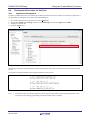
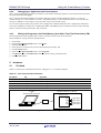
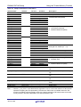
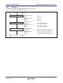
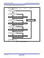
APPLICATION NOTE RX64M, RX71M Group Using the Trusted Memory Function R01AN2618EJ0101 Rev.1.01 Jun 18, 2015 Introduction This application note explains how to use the trusted memory function of RX64M and RX71M Group microcontrollers. The trusted memory (TM) function prevents unauthorized reading of programs stored in blocks 8 and 9 of the code flash memory or programming of additional data to those blocks. Target Devices RX64M Group • RX64M Group 177- and 176-pin versions, ROM capacity: 2 MB to 4 MB • RX64M Group 145- and 144-pin versions, ROM capacity: 2 MB to 4 MB • RX64M Group 100-pin version, ROM capacity: 2 MB to 4 MB RX71M Group • RX71M Group 177- and 176-pin versions, ROM capacity: 2 MB to 4 MB • RX71M Group 145- and 144-pin versions, ROM capacity: 2 MB to 4 MB • RX71M Group 100-pin version, ROM capacity: 2 MB to 4 MB When using this application note with other Renesas MCUs, careful evaluation is recommended after making modifications to comply with the alternate MCU. Contents 1. Specifications .................................................................................................................................... 2 2. Operation Confirmation Conditions ................................................................................................... 3 3. Reference Application Note .............................................................................................................. 3 4. TM Function Operation Example ...................................................................................................... 4 5. Hardware ......................................................................................................................................... 17 6. Software .......................................................................................................................................... 18 7. Cautions .......................................................................................................................................... 32 8. Sample Code................................................................................................................................... 33 9. Reference Documents..................................................................................................................... 33 R01AN2618EJ0101 Rev.1.01 Jun 18, 2015 Page 1 of 34 RX64M, RX71M Group 1. Using the Trusted Memory Function Specifications The description in this application note assumes a 1st user, who enables the TM function, and a 2nd user who uses the device with the TM function enabled. The 1st user writes a program to the area protected by TM, and then the 2nd user executes writes to areas other than the area protected by TM. Renesas Flash Programmer (RFP), a tool for programming flash memory, is used to write program data and to enable or disable the TM function. Running the sample code executes processing that turns LEDs on and off. Table 1.1 lists the peripheral functions used and their applications, and figure 1.1 is an overview diagram. Table 1.1 Peripheral Functions Used and Their Applications Peripheral Function Trusted memory function Application Prevents unauthorized reading of programs stored in blocks 8 and 9 of the code flash memory or programming of additional data to those blocks. 2nd user 1st user • Writes a program (encryption algorithm processing software, equipment control processing software processing software based on privileged knowhow, commercial middleware, etc.) to the TM protected area. • Enables the TM function. TM function enabled • Reads disabled • Additional programming disabled Provision of device RX64M/71M • Writes programs to areas other than the area protected by TM. • Embeds the device in a product. End user RX64M/71M Areas other than that protected by TM (programmed) Areas other than that protected by TM (not programmed) Area protected by TM (programmed) Release of product with embedded device 2nd user programs areas other than that protected by TM. Area protected by TM (programmed) Figure 1.1 Overview Diagram R01AN2618EJ0101 Rev.1.01 Jun 18, 2015 Page 2 of 34 RX64M, RX71M Group 2. Using the Trusted Memory Function Operation Confirmation Conditions The sample code accompanying this application note has been run and confirmed under the conditions below. Table 2.1 Operation Confirmation Conditions Item MCU used RAM capacity Code flash memory capacity Operating frequency Operating voltage Integrated development environment C compiler Contents R5F571MLCDFC (RX71M Group) 512 Kbytes 4 MB Main clock: 24 MHz PLL: 240 MHz (main clock divided by 1 and multiplied by 10) System clock (ICLK): 120 MHz (PLL divided by 2) Peripheral module clock A (PCLKA): 120 MHz (PLL divided by 2) Peripheral module clock B (PCLKB): 60 MHz (PLL divided by 4) Flash interface clock (FCLK): 60 MHz (PLL divided by 4) 3.3 V Renesas Electronics e2 studio Version: 4.0.0.26 Renesas Electronics C/C++ Compiler Package for RX Family V.2.03.00 Compiler options The integrated development environment default settings are used. iodefine.h version Endian Operating mode Processor mode Sample code version Board used Tools used 3. V1.00 Little endian Single-chip mode Supervisor mode Version 1.00 Renesas Starter Kit+ for RX71M (product type: R0K50571MSxxxBE) Renesas Flash Programmer V2.05 Reference Application Note For additional information associated with this document, refer to the following application notes. • RX71M Group Initial Settings Rev.1.00 (R01AN2459EJ) The initial settings function of the above application note is used in the sample code of this application note. The revision number is that which was current at the time of the preparation of this application note. If a newer version is available, replace the version included with this application note with the newer version. The latest version can be checked and downloaded from the Renesas Electronics website. R01AN2618EJ0101 Rev.1.01 Jun 18, 2015 Page 3 of 34 RX64M, RX71M Group 4. Using the Trusted Memory Function TM Function Operation Example The 1st user (who supplies the program in the area protected by TM) develops an application and creates a library file (.lib) containing the variables and function tables used by the program in the area protected by TM. After developing the application, the 1st user uses RFP to write the program to the area protected by TM and enables the TM function. The 1st user should provide the 2nd user with the specifications of the program in the area protected by TM, sample code section information, and the library file (.lib) created as described above. The 2nd user (application developer) uses the provided program specifications, section information, and library file (.lib) to develop an application. After developing the application, the 2nd user uses e2 studio to debug the application and uses RFP to write the program to an area other than that protected by TM. The 2nd user then embeds the device to which the program was written in the finished product and supplies it to the end user. Figure 4.1 shows the development sequence, and figure 4.2 is a block diagram. 1st user’s development sequence 2nd user’s development sequence Start Start 4.3.1 Application Development 4.4.1 Application Development 4.3.2 Creating a Library File Containing Variables and Function Tables 4.3.3 Enabling the TM Function (Writing the Program) 4.3.4 Disabling the TM Function* 4.4.2 Debugging an Application 4.4.3 Writing the Program to the Flash Memory (Area Other Than That Protected by TM) End (provision to end user) End (provision to 2nd user) Note: * To disable the TM function after it has been enabled, follow the instructions in 4.3.4, Disabling the TM Function. Figure 4.1 Development Sequence R01AN2618EJ0101 Rev.1.01 Jun 18, 2015 Page 4 of 34 RX64M, RX71M Group Using the Trusted Memory Function Area developed by user Area supplied by .lib file Section Address* SU SI B, B_1, B_2 R, R_1, R_2 0000 0000h B_TM, B_TM_1, B_TM_2 R_TM, R_TM_1, R_TM_2 0007 F000h Area written to by user 1st user’s address space 2nd user’s address space RAM RAM Uninitialized data, etc., developed by 2nd user Uninitialized data, etc., developed by 1st user 0008 0000h PResetPRG C, C_1, C_2 C$* D, D_1, D_2 W* L PIntPRG P FFC0 0000h C_TM, C_TM_1, C_TM_2 D_TM, D_TM_1, D_TM_2 FFFD 8000h P_TM_FUNC_01 FFFE 0000h Provision of .lib file Uninitialized data, etc., developed by 1st user Reserved area etc. Reserved area etc. ROM (blocks 133 to 10) ROM (blocks 133 to 10) Constants, etc., developed by 2nd user main() developed by 2nd user Constants, etc., developed by 1st user P_TM_FUNC_02 FFFE 0100h P_TM_FUNC_03 FFFE 0200h P_TM FFFE 0300h EXCEPTVECT FFFF FF80h RESETVECT FFFF FFFCh FFFF 0000h FFFF FFFFh Provision of .lib file Constants, etc., developed by 1st user Area protected by TM (blocks 9 and 8) Area protected by TM (blocks 9 and 8) R_tm_func_01() R_tm_func_01() R_tm_func_02() R_tm_func_02() R_tm_func_03() R_tm_func_03() TM internal function TM internal function ROM (blocks 7 to 0) ROM (blocks 7 to 0) Exception vector table Exception vector table Reset vector Reset vector Note: * The code flash memory capacity of the device used in this application note is 4 MB. Note that the actual code flash memory capacity differs depending on the product version. Figure 4.2 Block Diagram R01AN2618EJ0101 Rev.1.01 Jun 18, 2015 Page 5 of 34 RX64M, RX71M Group 4.1 Using the Trusted Memory Function Creating a New Project in RFP Renesas Flash Programmer (RFP) is a software application for programming flash memory. In this application note it is used to write a program to the area protected by TM and to enable and disable the TM function. The procedure for creating a new project in RFP is as follows: 1. 2. 3. 4. 5. 6. 7. Launch RFP. In the Welcome! dialog box, select Create new workspace and Basic mode. In the Using Target Microcontroller: list box, select RX as the group. Enter appropriate values for Workspace Name:, Project Name:, and Folder:, then click the Next button. Select E1 in the Tool: list box, then click the Next button. Check the box next to Power target from the emulator, select 3.3 V, then click the Next button. Next to Pin Outputs, check the boxes for io3 and io2 to specify the mode pins at connection, then click the OK button. 8. Select the emulator, then click the OK button. 9. Select Little Endian as the endian mode. 10. Enter settings in the Clock supply area, then click the OK button. 11. Select 2000000 bps in the Communication Speed (Recommended): list box. 12. Click the Finish button. RFP is available on the Renesas Electronics website. For detailed information on RFP, refer to Renesas Flash Programmer Flash memory programming software User’s Manual: Common and Renesas Flash Programmer Flash memory programming software User’s Manual: RH850, RX700 (Include RX64x). R01AN2618EJ0101 Rev.1.01 Jun 18, 2015 Page 6 of 34 RX64M, RX71M Group 4.2 Using the Trusted Memory Function Creating a New Project in e2 studio Both the 1st user and the 2nd user use e2 studio to make section settings, specify ROM options, and initialize sections. 4.2.1 Section Settings In order to clarify the areas of memory used for development by the 1st user and 2nd user, separate sections should be specified for use by the 1st user’s program in the area protected by TM and for application development by the 2nd user. Note that sections L and W are not used because they are #pragma sections that cannot be renamed. If switch statements are used, it is necessary to not specify table format (allocation to switch branching table area) but rather if_then format (allocation to program area). This setting causes switch statements to be allocated to the program area and written to the device. The switch statement code expansion setting is made by the 1st user only. The 1st user should provide the 2nd user with information on the sections used. The 2nd user should then make settings for the sections used by the 1st user, based on the information provided. It is important that the addresses be accurate when making section settings. It is also important that the sections used by the 2nd user be specified such that they do not overlap the areas used by the 1st user. For the section configuration used in this application note, see 6.3, Section Configuration. Figure 4.3 is a section diagram. R01AN2618EJ0101 Rev.1.01 Jun 18, 2015 Page 7 of 34 RX64M, RX71M Group Using the Trusted Memory Function Area developed by 1st user Area developed by 2nd user Area not usable for development Section SU SI B, B_1, B_2 R, R_1, R_2 B_TM, B_TM_1, B_TM_2 R_TM, R_TM_1, R_TM_2 P_TM_FUNC_01 P_TM_FUNC_02 P_TM_FUNC_03 P_TM 2nd user’s address space RAM RAM Uninitialized data Initialized data (RAM) TM uninitialized data TM initialized data (RAM) PResetPRG C, C_1, C_2 C$* D, D_1, D_2 W* L PIntPRG P C_TM, C_TM_1, C_TM_2 D_TM, D_TM_1, D_TM_2 1st user’s address space Provision of .lib file TM uninitialized data TM initialized data (RAM) Reserved area etc. Reserved area etc. ROM (blocks 133 to 10) ROM (blocks 133 to 10) Constant data Initialized data (ROM) Switch statement branching table Character string literal Main function, etc. TM constant data TM initialized data (ROM) Provision of .lib file Area protected by TM (blocks 9 and 8) Area protected by TM (blocks 9 and 8) TM API function* TM internal function* EXCEPTVECT RESETVECT TM constant data TM initialized data (ROM) Programmed by RFP TM API function TM internal function ROM (blocks 7 to 0) ROM (blocks 7 to 0) Exception vector table Exception vector table Reset vector Reset vector Note: * Switch statements are expanded in if_then format, so they are allocated to sections in the area protected by TM (API function section P_TM_FUNC_xx and internal function section P_TM). Figure 4.3 Section Diagram R01AN2618EJ0101 Rev.1.01 Jun 18, 2015 Page 8 of 34 RX64M, RX71M Group Using the Trusted Memory Function The procedure for making section settings is described below: 1. 2. 3. 4. In e2 studio, right-click the target project and select Properties. Under C/C++ Build select Settings. Switch to the Tool Settings tab and select Section under Linker. Enter settings for each section. Click the Apply button. R01AN2618EJ0101 Rev.1.01 Jun 18, 2015 Page 9 of 34 RX64M, RX71M Group Using the Trusted Memory Function The procedure for setting the code expansion format for switch statements is described below: 1. 2. 3. 4. In e2 studio, right-click the target project and select Properties. Under C/C++ Build select Settings. Switch to the Tool Settings tab and select Advanced under Optimize. In the Switch statement: list box, select if then. Click the Apply button. R01AN2618EJ0101 Rev.1.01 Jun 18, 2015 Page 10 of 34 RX64M, RX71M Group 4.2.2 Using the Trusted Memory Function ROM Option Settings ROM options are used to secure areas in ROM and RAM for the initialized data area and to relocate symbols defined in ROM sections to addresses in RAM sections. ROM option settings are specified by default for sections D and R only. When creating a new project, it is necessary to enter ROM option settings for the initialized data areas (D_TM and R_TM) used by the 1st user. The procedure for setting ROM options is described below: 1. In e2 studio, right-click the target project and select Properties. 2. Under C/C++ Build select Settings. Switch to the Tool Settings tab and select Output under Linker. 3. Add the sections to be mapped from ROM to RAM. (In this application note the additions are D_TM = R_TM, D_TM_1 = R_TM_1, and D_TM_2 = R_TM_2.) 4. Click the Apply button. For detailed information about ROM options, see CC-RX V2.03.00 RX Family C/C++ Compiler: User’s Manual. R01AN2618EJ0101 Rev.1.01 Jun 18, 2015 Page 11 of 34 RX64M, RX71M Group 4.2.3 Using the Trusted Memory Function Section Initialization When the _INITSCT function in reset_program.c, a file generated automatically by e2 studio, is called, uninitialized data sections are zero-initialized and initialized data sections are copied from the ROM area to the RAM area. The user must declare the sections to be initialized in section initialization tables (DTBL and BTBL). Add the lines indicated below to the section initialization tables in the file dbsct.c, which is generated automatically by e2 studio. For detailed information about section initialization, see CC-RX V2.03.00 RX Family C/C++ Compiler: User’s Manual. R01AN2618EJ0101 Rev.1.01 Jun 18, 2015 Page 12 of 34 RX64M, RX71M Group 4.3 4.3.1 Using the Trusted Memory Function Development Procedure for 1st User Application Development Generally speaking, symbols are used to call functions, but the 2nd user cannot use this method to access functions in the area protected by TM because the 2nd user is not provided with symbol information for these functions. In order to access functions in the area protected by TM, the 2nd user requires address information for these functions. The 1st user must therefore prepare function tables containing function address information for the area protected by TM. The function tables are allocated to the constant area, so they are provided to the 2nd user in the library file (.lib). This enables the 2nd user to call functions located in the area protected by TM by utilizing the function tables. API functions in the area protected by TM are assigned sections and addresses individually. The first user should store the section start address of each API function in the function table. Information other than variables and function tables is omitted when the library file is created, so it is not possible to use function symbols in function tables. An example of a function table is shown below: When the TM function is enabled, performing data access to the area protected by TM causes zeros to be read, so only section P should be allocated to the area protected by TM. All areas to which data access will be performed (section C, etc.) should be assigned to areas other than the area protected by TM. This application note includes confirmation of data access operation when accessing the area protected by TM while the TM function is enabled. For information on data access operation when the TM function is enabled, see 6.1.1, Data Access. 4.3.2 Creating a Library File Containing Variables and Function Tables To access functions in the area protected by TM, the 2nd user requires address information for these functions. The 1st user must therefore prepare and supply to the 2nd user a library file (.lib) containing variables and function tables for the area protected by TM. The library file is created with the sample code rx71m_tm_user1_lib by building the file tm_api.c, with information other than global variables, const variables, and function tables for the area protected by TM removed. The procedure for creating a new library file project is described below: 1. 2. 3. 4. 5. 6. From the e2 studio File menu, select New > C Project. In the Project type: list box, select Static Library (Renesas) > Sample Project. In the Toolchains: list box, select Renesas RXC Toolchain. Enter a name for the project, then click the Next button. For ISA type, select RXv2 architecture. Click the Finish button. R01AN2618EJ0101 Rev.1.01 Jun 18, 2015 Page 13 of 34 RX64M, RX71M Group 4.3.3 Using the Trusted Memory Function Enabling the TM Function RFP is used to enable the TM function. Enabling of the TM and program writing to the area protected by TM take place at the same time.*1*2 The 1st user creates mot files from which all code except that related to the TM enable flag register (TMEF register), TM identification data register (TMINF register), and area protected by TM has been removed, and writes them to the target device. The TM function is enabled by setting the TMEF bits in the TMEF register to 000b.*3 The TMINF register stores the code used to identify programs in the area protected by TM. To make settings to the TMEF register and TMINF register, make the modifications shown below to the file vector_table.c, which is generated automatically by e2 studio. The procedure for writing the mot files to the target device with REP is described below: 1. 2. 3. 4. 5. 6. Launch RFP. From the RFP Microcontroller menu, select All Erase. Click the Start button. From the RFP Microcontroller menu, select Program. Click Browse next to User/Data area: and select the previously created mot files. Click the Start button. For details on enabling the TM function, see “How to Enable the TM Function” in the “Flash Memory” section in RX64M Group User’s Manual: Hardware or RX71M Group User’s Manual: Hardware. For detailed information on RFP, refer to Renesas Flash Programmer Flash memory programming software User’s Manual: Common and Renesas Flash Programmer Flash memory programming software User’s Manual: RH850, RX700 (Include RX64x). Notes: 1. It is also possible to enable the TM function after writing a program to the area protected by TM. To accomplish this, create a mot file containing the TMEF register code only and proceed from step 4 to write it to the microcontroller. 2. It is also possible to enable the TM function internally by means of self-programming. 3. It is not possible to enable the TM function by using the e2 studio environment (download). RFP must be used to write to the microcontroller. R01AN2618EJ0101 Rev.1.01 Jun 18, 2015 Page 14 of 34 RX64M, RX71M Group 4.3.4 Using the Trusted Memory Function Disabling the TM Function The TM function can be disabled by first erasing the data flash memory, user boot area, and the areas other than that protected by TM (blocks 8 and 9), and then issuing the clear configuration command. When the clear configuration command is issued, the configuration settings area, including the TMEF and TMINF registers, and the code flash memory, which is the area protected by TM, are erased. The procedure for disabling the TM function is described below: 1. 2. 3. 4. 5. 6. 7. Launch RFP. From the RFP Microcontroller menu, select Set Project. Select the Other Settings tab. Under Command Options, set Clear Configuration After All Erase to True. Click the OK button. From the Microcontroller menu, select All Erase. Click the Start button. R01AN2618EJ0101 Rev.1.01 Jun 18, 2015 Page 15 of 34 RX64M, RX71M Group 4.4 4.4.1 Using the Trusted Memory Function Development Procedure for 2nd User Application Development Using the provided library file (.lib) containing variables and function tables, the 2nd user can develop an application.* The procedure for linking the library file (.lib) is described below: 1. 2. 3. 4. In e2 studio, right-click the target project and select Properties. Under C/C++ Build select Settings. Switch to the Tool Settings tab and select Input under Linker. Add the provided .lib file. Click the Apply button. The 2nd user should use the function tables in the provided library file (.lib) to call API functions in the area protected by TM. An example of calling API functions using function tables is shown below. Note: * The 2nd user must not allocate programs to the area protected by TM when developing applications. This will result in errors during programming because the TM function is enabled. R01AN2618EJ0101 Rev.1.01 Jun 18, 2015 Page 16 of 34 RX64M, RX71M Group 4.4.2 Using the Trusted Memory Function Debugging an Application after Development The e2 studio integrated development environment can be used to download programs to areas other than that protected by TM for application debugging. The e2 studio integrated development environment offers the options when downloading programs to “overwrite without erasing” or to “erase and then overwrite.” The default setting is “erase and then overwrite,” but when the TM function is enabled it is not possible to erase programs in the area protected by TM. To erase the area protected by TM, issue the clear configuration command. When the clear configuration command is issued, the configuration settings area, including the TMEF and TMINF registers, and blocks 8 and 9 of the code flash memory, which is the area protected by TM, are erased. 4.4.3 Writing the Program to the Flash Memory (Area Other Than That Protected by TM) Following application development, RFP is used to write the mot files to the microcontroller. The procedure for writing the file is described below: 1. 2. 3. 4. 5. 6. 7. 8. Launch RFP. From the RFP Microcontroller menu, select Erase. Click the Start button. Check the boxes for the blocks in areas other than that protected by TM. Click the Erase button. From the RFP Microcontroller menu, select Program. Click Browse next to User/Data area: and select the previously created mot files. Click the Start button. 5. 5.1 Hardware Pin Used Table 5.1 lists the pins used and their functions, and figure 5.1 is a connection diagram. Table 5.1 Pins Used and Their Functions Pin Name P03 P05 P26 P27 I/O Output Output Output Output Function LED0 output LED1 output LED2 output LED3 output e2 studio or Renesas Flash Programmer Renesas Starter Kit+ for RX71M RX71M Group E1 P03 P05 P26 P27 LED0 output LED1 output LED2 output LED3 output PC Figure 5.1 Connection Diagram R01AN2618EJ0101 Rev.1.01 Jun 18, 2015 Page 17 of 34 RX64M, RX71M Group 6. Using the Trusted Memory Function Software 6.1 Operation Overview Operation when rx71m_tm_user1.mot and rx71m_tm_user2.mot have been written to the target device is described below. After initial settings are made by the main function, the LEDs turn on in predetermined patterns. The tables below show the LED patterns associated with the area protected by TM and with the areas not protected by TM. Figure 6.1 shows the LED tables. After the display of the patterns, all the LEDs turn off. Area Protected by TM − LED Table Programmed Value LED Bit 3 Bit 2 Bit 1 Bit 0 Area Not Protected by TM − LED Table LED Programmed Value Pattern 1 0x09 0x01 Pattern 2 0x06 0x02 Pattern 3 0x09 0x04 Pattern 4 0x06 0x08 Bit 3 Bit 2 Bit 1 Bit 0 : LED on : LED off Figure 6.1 LED Table 6.1.1 Data Access The LED patterns in the table for the area protected by TM differ when the TM function is enabled and when it is disabled. When the TM function is enabled, performing data access to the area protected by TM results in all zeros being read, rather than the programmed value. The program associated with this application note turns all LEDs on when the pattern value 0x00 is read. Figure 6.2 shows the different LED patterns when the TM function is enabled and when it is disabled. Area Protected by TM − LED Table TM Function Enabled TM Function Disabled Programmed Value Read Value Pattern 1 0x09 Pattern 2 LED Programmed Value Read Value 0x09 0x09 0x00 0x06 0x06 0x06 0x00 Pattern 3 0x09 0x09 0x09 0x00 Pattern 4 0x06 0x06 0x06 0x00 Bit 3 Bit 2 Bit 1 Bit 0 : LED on LED Bit 3 Bit 2 Bit Bit 0 : LED off Figure 6.2 Difference in LED Patterns when TM Function Is Enabled and Disabled R01AN2618EJ0101 Rev.1.01 Jun 18, 2015 Page 18 of 34 RX64M, RX71M Group 6.2 Using the Trusted Memory Function Sample Code Configuration Table 6.1 lists the sample code supplied with this application note. Table 6.1 Sample Code Supplied with Application Note File Name rx71m_tm_user1 rx71m_tm_user1_lib rx71m_tm_user2 6.3 Outline Project developed by 1st user .lib file generation project provided to 2nd user Project developed by 2nd user Remarks Section Configuration Table 6.2 lists section information for the sample code. For information on how to add, modify, or erase sections, see the latest version of the RX Family C/C++ Compiler: User’s Manual. R01AN2618EJ0101 Rev.1.01 Jun 18, 2015 Page 19 of 34 RX64M, RX71M Group Using the Trusted Memory Function Table 6.2 Sample Code Section Information Section Name SU SI B_1 R_1 B_2 R_2 B R B_TM_1 R_TM_1 B_TM_2 R_TM_2 B_TM R_TM PResetPRG C_1 C_2 C C$* D_1 D_2 D W* L PIntPRG P C_TM_1 C_TM_2 C_TM D_TM_1 D_TM_2 D_TM P_TM_FUNC_01 Address 0000 0004 0007 F000 FFC0 0000 FFFD F000 FFFE 0000 1st User Addition Addition Addition Addition Addition Addition Addition Addition Change Addition Addition Addition Addition Addition Addition Addition 2nd User Addition Addition Addition Addition Addition Addition Addition Addition Change Addition Addition Addition Addition Addition Addition Addition Description User stack area Interrupt stack area Uninitialized data area Initialized data area (RAM) Used by area protected by TM • Uninitialized data area • Initialized data area (RAM) Power-on reset PC Constant area Initialized data area (ROM) Changed from default (D* → D) Switch statement branching table area Literal area Interrupt vector table Program area Used by area protected by TM • Constant area Used by area protected by TM • Initialized data area (ROM) API function 01 in area protected by TM P_TM_FUNC_02 FFFE 0100 Addition Addition API function 02 in area protected by TM P_TM_FUNC_03 FFFE 0200 Addition Addition API function 03 in area protected by TM P_TM FFFE 0300 Addition Not needed Internal function in area protected by TM Note 1 (C_TM_TEST*) (FFFE 0400) (Addition) (Addition) (Area protected by TM − constant area) EXCEPTVECT FFFF FF80 Exception vector table RESETVECT FFFF FFFC Reset vector : Default Note: 1. Section C_TM_TEST* is provided with this application note to confirm the behavior of data access operations targeting the area protected by TM when the TM function is enabled. When the TM function is enabled, performing data access to the area protected by TM causes zeros to be read, so only section P should be allocated to the area protected by TM. R01AN2618EJ0101 Rev.1.01 Jun 18, 2015 Page 20 of 34 RX64M, RX71M Group 6.4 Using the Trusted Memory Function 1st User 6.4.1 File Composition Tables 6.3 and 6.4 list the files used in the sample code. Files generated by the integrated development environment are not included in this table. Table 6.3 Files Used in the Sample Code (rx71m_tm_user1) File Name r_tm_api.c r_tm_api.h Outline Program in area protected by TM Header file of r_tm_api.c Remarks Table 6.4 Files Used in the Sample Code (rx71m_tm_user1_lib) File Name r_tm_api.c 6.4.2 Outline Program in area protected by TM Remarks All information other than variables and function tables deleted Option-Setting Memory Table 6.5 lists the option-setting memory configured in the sample code. When necessary, set a value suited to the user system. Table 6.5 Option-Setting Memory Configured in the Sample Code Symbol OFS1 Address 0012 006Fh to 0012 006Ch Contents Voltage monitor 0 reset disabled after a reset HOCO oscillation disabled after a reset OFS0 0012 006Bh to 0012 0068h FFFF FFFFh IWDT stopped after a reset WDT stopped after a reset MDE 0012 0067h to 0012 0064h FFFF FFFFh Little endian 1 TMINF* 0012 0063h to 0012 0060h 544D 3031h ASCII code: TM01 TMEF*1*2 0012 004Bh to 0012 0048h F8FF FFFFh FFFF FFFFh: TM function disabled F8FF FFFFh: TM function enabled Notes: 1. See 4.3.3, Enabling the TM Function, and 4.3.4, Disabling the TM Function, for information on making settings to the TMEF and TMINF registers. 2. It is not possible to make settings to the TMEF register by using the e2 studio environment (download). RFP must be used to make settings to the TMEF register. R01AN2618EJ0101 Rev.1.01 Jun 18, 2015 Setting Value FFFF FFFFh Page 21 of 34 RX64M, RX71M Group 6.4.3 Using the Trusted Memory Function Constants Table 6.6 lists the constants used in the sample code. Table 6.6 Constants Used in the Sample Code Constant Name LED_ON LED_OFF LED0_REG_PODR LED1_REG_PODR LED2_REG_PODR LED3_REG_PODR LED0_REG_PDR LED1_REG_PDR LED2_REG_PDR LED3_REG_PDR LED0_REG_PMR LED1_REG_PMR LED2_REG_PMR LED3_REG_PMR 6.4.4 Setting Value 0 1 PORT0.PODR.BIT.B3 PORT0.PODR.BIT.B5 PORT2.PODR.BIT.B6 PORT2.PODR.BIT.B7 PORT0.PDR.BIT.B3 PORT0.PDR.BIT.B5 PORT2.PDR.BIT.B6 PORT2.PDR.BIT.B7 PORT0.PMR.BIT.B3 PORT0.PMR.BIT.B5 PORT2.PMR.BIT.B6 PORT2.PMR.BIT.B7 Description LED output data: On LED output data: Off LED0 output data storage bit LED1 output data storage bit LED2 output data storage bit LED3 output data storage bit LED0 direction control bit LED1 direction control bit LED2 direction control bit LED3 direction control bit LED0 pin mode control bit LED1 pin mode control bit LED2 pin mode control bit LED3 pin mode control bit Variables Table 6.7 lists the const variables. Table 6.7 const Variables Type const uint8_t const uint8_t const uint8_t 6.4.5 Variable Name g_test_tm_led_table[] g_tm_led_table[] g_led_pattern_num Description LED table of area protected by TM LED table of area not protected by TM Number of LED patterns Function Used main main main Functions Table 6.8 lists the functions used in the sample code. Table 6.8 Functions Used in the Sample Code Function R_TM_PortInit R_TM_SetLedPattern R_TM_LedOff tm_led_on R01AN2618EJ0101 Rev.1.01 Jun 18, 2015 Outline Initial port settings (API function in area protected by TM) Display LED pattern (API function in area protected by TM) Turn off all LEDs (API function in area protected by TM) Turn on all LEDs (internal function in TM function area) Page 22 of 34 RX64M, RX71M Group 6.4.6 Using the Trusted Memory Function Function Tables Table 6.9 lists the function tables. Table 6.9 Function Tables Type void Function Pointer Name tm_func_table1[] Argument void void tm_func_table2[] uint8_t argument 6.4.7 Storage Address __sectop(“P_TM_FUNC_01”), __sectop(“P_TM_FUNC_03”) __sectop(“P_TM_FUNC_02”) Function Specifications The following tables lists the sample code function specifications. R_TM_PortInit Outline Header Declaration Description Arguments Return Value Initial port settings (API function in area protected by TM) r_tm_api.h void R_TM_PortInit (void) Performs initial LED port settings. None None R_TM_SetLedPattern Outline Header Declaration Description Arguments Return Value Display LED pattern (API function in area protected by TM) r_tm_api.h void R_TM_SetLedPattern (uint8_t pattern) Outputs an LED pattern. All LEDs turn on when the LED pattern is 0x00. uint8_t pattern LED pattern None R_TM_LedOff Outline Header Declaration Description Arguments Return Value Turn off all LEDs (API function in area protected by TM) r_tm_api.h void R_TM_LedOff (void) Turns off all LEDs. None None tm_led_off Outline Header Declaration Description Arguments Return Value Turn on all LEDs (internal function in TM function area) r_tm_api.h void tm_led_on (void) Turns on all LEDs. None None R01AN2618EJ0101 Rev.1.01 Jun 18, 2015 Page 23 of 34 RX64M, RX71M Group 6.4.8 Using the Trusted Memory Function Flowcharts (1) Initial Port Settings (API Function in Area Protected by TM) Figure 6.3 is a flowchart of the initial port settings. R_TM_PortInit Set port output data Set port direction Set port mode PORT0.PODR register B3 bit ← 1 B5 bit ← 1 PORT2.PODR register B6 bit ← 1 B7 bit ← 1 PORT0.PDR register B3 bit ← 1 B5 bit ← 1 PORT2.PDR register B6 bit ← 1 B7 bit ← 1 PORT0.PMR register B3 bit ← 0 B5 bit ← 0 PORT2.PMR register B6 bit ← 0 B7 bit ← 0 :LED0: Off :LED1: Off :LED2: Off :LED3: Off :LED0: Used as output port :LED1: Used as output port :LED2: Used as output port :LED3: Used as output port :LED0: Used as general-purpose I/O port :LED1: Used as general-purpose I/O port :LED2: Used as general-purpose I/O port :LED3: Used as general-purpose I/O port return Figure 6.3 Initial Port Settings R01AN2618EJ0101 Rev.1.01 Jun 18, 2015 Page 24 of 34 RX64M, RX71M Group Using the Trusted Memory Function (2) Display LED Pattern (API Function in Area Protected by TM) Figure 6.4 is a flowchart of the processing to display LED patterns. [Argument] uint8_t R_TM_SetLedPattern What is the LED pattern? pattern : LED pattern 0x00 Other than 0x00 Is value of bit 0 of LED pattern 1? No Yes LED0 on Is value of bit 1 of LED pattern 1? LED0 off Turn on all LEDs tm_led_on() No Yes LED1 on Is value of bit 2 of LED pattern 1? LED1 off No Yes LED2 on Is value of bit 3 of LED pattern 1? LED2 off No Yes LED3 on LED3 off return Figure 6.4 Display LED Pattern R01AN2618EJ0101 Rev.1.01 Jun 18, 2015 Page 25 of 34 RX64M, RX71M Group Using the Trusted Memory Function (3) Turn Off All LEDs (API Function in Area Protected by TM) Figure 6.5 is a flowchart of the processing to turn off all LEDs. R_TM_LedOff Turn off all LEDs return Figure 6.5 Turn Off All LEDs (4) Turn On All LEDs (Internal Function in TM Function Area) Figure 6.6 is a flowchart of the processing to turn on all LEDs. tm_led_on Turn on all LEDs return Figure 6.6 Turn On All LEDs R01AN2618EJ0101 Rev.1.01 Jun 18, 2015 Page 26 of 34 RX64M, RX71M Group 6.5 6.5.1 Using the Trusted Memory Function 2nd User File Composition Tables 6.10 and 6.11 list the files used in the sample code. Files generated by the integrated development environment are not included in this table. Table 6.10 Files Used in the Sample Code (c File and h File) File Name main.c r_init_stop_module.c r_init_stop_module.h r_init_non_existent_port.c r_init_non_existent_port.h r_init_clock.c r_init_clock.h Outline Main processing routine Stop peripheral functions still running after reset Header file of r_init_stop_module.c Initial settings of nonexistent ports Header file of r_init_non_existent_port.c Initial clock settings Header file of r_init_clock.c Remarks Table 6.11 Files Used in the Sample Code (use File) File Name rx71m_tm_user1_lib.lib 6.5.2 Outline Library file provided by 1st user Remarks Option-Setting Memory Table 6.12 lists the option-setting memory configured in the sample code. When necessary, set a value suited to the user system. Table 6.12 Option-Setting Memory Configured in the Sample Code Symbol OFS1 Address 0012 006Fh to 0012 006Ch Description Voltage monitor 0 reset disabled after a reset HOCO oscillation disabled after a reset OFS0 0012 006Bh to 0012 0068h FFFF FFFFh IWDT stopped after a reset WDT stopped after a reset MDE 0012 0067h to 0012 0064h FFFF FFFFh Little endian 1 2 TMINF* * 0012 0063h to 0012 0060h FFFF FFFFh TM identification data TMEF*1*2 0012 004Bh to 0012 0048h FFFF FFFFh FFFF FFFFh: TM function disabled F8FF FFFFh: TM function enabled Notes: 1. When the TM function is enabled, values set by the 1st user are stored. 2. See 4.3.3, Enabling the TM Function, and 4.3.4, Disabling the TM Function, for information on making settings to the TMEF and TMINF registers. R01AN2618EJ0101 Rev.1.01 Jun 18, 2015 Setting Value FFFF FFFFh Page 27 of 34 RX64M, RX71M Group 6.5.3 Using the Trusted Memory Function Constants Table 6.13 lists the constants used in the sample code. Table 6.13 Constants Used in the Sample Code Constant Name R_TM_PORT_INIT R_TM_LED_OFF R_TM_SET_LED_PATTERN 6.5.4 Setting Value 0 1 0 Description Function table 1 element Function table 1 element Function table 2 element Functions Table 6.14 lists the functions used in the sample code. Table 6.14 Functions Used in the Sample Code Function main R_INIT_StopModule R_INIT_NonExistentPort R_INIT_Clock led_control 6.5.5 Outline Main processing routine Stop peripheral functions still running after reset Initial settings of nonexistent ports Initial clock settings LED control Function Specifications The following tables lists the sample code function specifications. main Outline Header Declaration Description Arguments Return Value R_INIT_StopModule Outline Header Declaration Description Arguments Return Value Outline Main processing routine None void main(void) After making initial settings, accesses the area protected by TM (LED display processing). None None Stop peripheral functions still running after reset r_init_stop_module.h void R_INIT_StopModule(void) Makes settings to transition to the module-stop state. None None The sample code does not perform the transition to the module-stop state. For detailed information about this function, see the application note RX71M Group Initial Settings Example, Rev. 1.00. R01AN2618EJ0101 Rev.1.01 Jun 18, 2015 Page 28 of 34 RX64M, RX71M Group Using the Trusted Memory Function R_INIT_NonExistentPort Initial settings of nonexistent ports Outline r_init_non_existent_port.h Header void R_INIT_NonExistentPort(void) Declaration Makes initial settings to port direction registers corresponding to pins of ports that do Description not exist. None Arguments None Return Value The settings in the sample code are for 176-pin microcontrollers (PIN_SIZE=176). Notes After calling this function, when writing in byte units to PDR or PODR registers containing nonexistent ports, set the direction control bits and port output data storage bits corresponding to the nonexistent ports to 1 and 0, respectively. For detailed information about this function, see the application note RX71M Group Initial Settings Example, Rev. 1.00. R_INIT_Clock Outline Header Declaration Description Arguments Return Value Notes led_control Outline Header Declaration Description Arguments Return Value Initial clock settings r_init_clock.h void R_INIT_Clock(void) Makes initial clock settings. None None In the sample code PLL is set as the system clock and no subclock is used. For detailed information about this function, see the application note RX71M Group Initial Settings Example, Rev. 1.00. LED control (API function in area protected by TM) None static void tm_control (const uint8_t *table, const uint8_t pattern_num) Outputs LED patterns from the LED table in sequence. const uint8_t *table LED table const uint8_t pattern_num Number of LED patterns None R01AN2618EJ0101 Rev.1.01 Jun 18, 2015 Page 29 of 34 RX64M, RX71M Group 6.5.6 Using the Trusted Memory Function Flowcharts (1) Main Processing Routine Figure 6.7 is a flowchart of the main processing routine. main Disable maskable interrupts I flag ← 0 Stop peripheral functions still running after reset R_INIT_StopModule() Initial settings of nonexistent ports R_INIT_NonExistentPort() Initial clock settings R_INIT_Clock() Enable maskable interrupts I flag ← 1 Initial port settings* R_TM_PortInit() LED control led_control() Less than 0x05 Uses LED table in area protected by TM Value of cnt? 0x05 or more LED control led_control() Less than 0x05 Uses LED table in area other than that protected by TM Value of cnt? 0x05 or more Turn off LED* R_TM_LedOff() Note: * The 2nd user uses function tables to call API functions in the area protected by TM. Figure 6.7 Main Processing Routine R01AN2618EJ0101 Rev.1.01 Jun 18, 2015 Page 30 of 34 RX64M, RX71M Group Using the Trusted Memory Function (2) LED Control Figure 6.8 is a flowchart of the LED control processing. [Arguments] const uint8_t const uint8_t led_control *table pattern_num : LED table : Number of LED patterns Display LED pattern* R_TM_SetLedPattern() Increment LED table address LED display wait time Less than pattern_num Number of LED patterns? pattern_num or more return Note: * The 2nd user uses function tables to call API functions in the area protected by TM. Figure 6.8 LED Control R01AN2618EJ0101 Rev.1.01 Jun 18, 2015 Page 31 of 34 RX64M, RX71M Group 7. Using the Trusted Memory Function Cautions 7.1 Initial Settings Example The sample code referenced in this application note includes partial modifications to the sample code provided in the application note RX71M Group Initial Settings Example. When upgrading to the latest version of the initial settings sample code, make sure to make the modifications listed below. Table 7.1 lists the modifications to the initial settings sample code. Table 7.1 Initial Settings Constants (r_init_clock.h) Modified in Sample Code Constant Name REG_SCKCR Value Before Change 20C2 1222h (PLL selected) Value After Change 21C2 1222h (PLL selected) REG_MEMWAIT MEMWAIT_1WAIT MEMWAIT_0WAIT 7.2 Description Internal clock division ratio (SCKCR register setting value) Before change: ICLK = 240 MHz After change: ICLK = 120 MHz Memory wait cycles Before change: 1 wait cycle After change: 0 wait cycles Other The 1st user can also provide the 2nd user with a section information file (.esi) containing section information. To do this, the 1st user should export a section information file (.esi) from e2 studio. The procedure for creating a section information file (.esi) is described below: 1. 2. 3. 4. In e2 studio, right-click the target project and select Properties. Under C/C++ Build select Settings. Switch to the Tool Settings tab and select Section under Linker. Click Export. Select a destination to save the file. The 2nd user can then use e2 studio to import the section information file (.esi).* The procedure for importing a section information file (.esi) is described below: 1. 2. 3. 4. In e2 studio, right-click the target project and select Properties. Under C/C++ Build select Settings. Switch to the Tool Settings tab and select Section under Linker. Click Import. Open the provided section information file (.esi). Note: * Care should be exercised, because importing a section information file (.esi) causes all existing section settings to be erased and overwritten with the new ones. R01AN2618EJ0101 Rev.1.01 Jun 18, 2015 Page 32 of 34 RX64M, RX71M Group 8. Using the Trusted Memory Function Sample Code Sample code can be downloaded from the Renesas Electronics website. 9. Reference Documents User’s Manual: Hardware RX64M Group User’s Manual: Hardware (R01UH0377EJ) RX71M Group User’s Manual: Hardware (R01UH0493EJ) (The latest version can be downloaded from the Renesas Electronics website.) User’s Manual: Flash Memory RX64M Group, RX71M Group Flash Memory User’s Manual: Hardware Interface (R01UH0435EJ) (The latest version can be downloaded from the Renesas Electronics website.) User’s Manual: Renesas Flash Programmer Renesas Flash Programmer V2.05 Flash memory programming software User’s Manual: Common (R20UT2906EJ) Renesas Flash Programmer V2.05 Flash memory programming software User’s Manual: RH850, RX700 (Include RX64M) (R20UT2909EJ) (The latest version can be downloaded from the Renesas Electronics website.) Technical Update/Technical News (The latest information can be downloaded from the Renesas Electronics website.) User’s Manual: Development Tools CC-RX V2.03.00 RX Family C/C++ Compiler User’s Manual (R20UT3248EJ) (The latest version can be downloaded from the Renesas Electronics website.) R01AN2618EJ0101 Rev.1.01 Jun 18, 2015 Page 33 of 34 RX64M, RX71M Group Using the Trusted Memory Function Website and Support Renesas Electronics Website http://www.renesas.com/ Inquiries http://www.renesas.com/contact/ All trademarks and registered trademarks are the property of their respective owners. R01AN2618EJ0101 Rev.1.01 Jun 18, 2015 Page 34 of 34 Revision History Rev. 1.00 1.01 Date Apr 01, 2015 Jun 18, 2015 Description Page Summary First edition issued 3 Integrated development environment changed in table 2.1 Operation Confirmation Conditions 17 4.4.2 Debugging an Application after Development changed Information on debugging removed from 7.2 A-1 General Precautions in the Handling of MPU/MCU Products The following usage notes are applicable to all MPU/MCU products from Renesas. For detailed usage notes on the products covered by this document, refer to the relevant sections of the document as well as any technical updates that have been issued for the products. 1. Handling of Unused Pins Handle unused pins in accord with the directions given under Handling of Unused Pins in the manual. The input pins of CMOS products are generally in the high-impedance state. In operation with an unused pin in the open-circuit state, extra electromagnetic noise is induced in the vicinity of LSI, an associated shoot-through current flows internally, and malfunctions occur due to the false recognition of the pin state as an input signal become possible. Unused pins should be handled as described under Handling of Unused Pins in the manual. 2. Processing at Power-on The state of the product is undefined at the moment when power is supplied. The states of internal circuits in the LSI are indeterminate and the states of register settings and pins are undefined at the moment when power is supplied. In a finished product where the reset signal is applied to the external reset pin, the states of pins are not guaranteed from the moment when power is supplied until the reset process is completed. In a similar way, the states of pins in a product that is reset by an on-chip power-on reset function are not guaranteed from the moment when power is supplied until the power reaches the level at which resetting has been specified. 3. Prohibition of Access to Reserved Addresses Access to reserved addresses is prohibited. The reserved addresses are provided for the possible future expansion of functions. Do not access these addresses; the correct operation of LSI is not guaranteed if they are accessed. 4. Clock Signals After applying a reset, only release the reset line after the operating clock signal has become stable. When switching the clock signal during program execution, wait until the target clock signal has stabilized. When the clock signal is generated with an external resonator (or from an external oscillator) during a reset, ensure that the reset line is only released after full stabilization of the clock signal. Moreover, when switching to a clock signal produced with an external resonator (or by an external oscillator) while program execution is in progress, wait until the target clock signal is stable. 5. Differences between Products Before changing from one product to another, i.e. to a product with a different type number, confirm that the change will not lead to problems. The characteristics of an MPU or MCU in the same group but having a different part number may differ in terms of the internal memory capacity, layout pattern, and other factors, which can affect the ranges of electrical characteristics, such as characteristic values, operating margins, immunity to noise, and amount of radiated noise. When changing to a product with a different part number, implement a system-evaluation test for the given product. Notice 1. Descriptions of circuits, software and other related information in this document are provided only to illustrate the operation of semiconductor products and application examples. You are fully responsible for the incorporation of these circuits, software, and information in the design of your equipment. Renesas Electronics assumes no responsibility for any losses incurred by you or third parties arising from the use of these circuits, software, or information. 2. Renesas Electronics has used reasonable care in preparing the information included in this document, but Renesas Electronics does not warrant that such information is error free. Renesas Electronics 3. Renesas Electronics does not assume any liability for infringement of patents, copyrights, or other intellectual property rights of third parties by or arising from the use of Renesas Electronics products or assumes no liability whatsoever for any damages incurred by you resulting from errors in or omissions from the information included herein. technical information described in this document. No license, express, implied or otherwise, is granted hereby under any patents, copyrights or other intellectual property rights of Renesas Electronics or others. 4. You should not alter, modify, copy, or otherwise misappropriate any Renesas Electronics product, whether in whole or in part. Renesas Electronics assumes no responsibility for any losses incurred by you or 5. Renesas Electronics products are classified according to the following two quality grades: "Standard" and "High Quality". The recommended applications for each Renesas Electronics product depends on third parties arising from such alteration, modification, copy or otherwise misappropriation of Renesas Electronics product. the product's quality grade, as indicated below. "Standard": Computers; office equipment; communications equipment; test and measurement equipment; audio and visual equipment; home electronic appliances; machine tools; personal electronic equipment; and industrial robots etc. "High Quality": Transportation equipment (automobiles, trains, ships, etc.); traffic control systems; anti-disaster systems; anti-crime systems; and safety equipment etc. Renesas Electronics products are neither intended nor authorized for use in products or systems that may pose a direct threat to human life or bodily injury (artificial life support devices or systems, surgical implantations etc.), or may cause serious property damages (nuclear reactor control systems, military equipment etc.). You must check the quality grade of each Renesas Electronics product before using it in a particular application. You may not use any Renesas Electronics product for any application for which it is not intended. Renesas Electronics shall not be in any way liable for any damages or losses incurred by you or third parties arising from the use of any Renesas Electronics product for which the product is not intended by Renesas Electronics. 6. You should use the Renesas Electronics products described in this document within the range specified by Renesas Electronics, especially with respect to the maximum rating, operating supply voltage range, movement power voltage range, heat radiation characteristics, installation and other product characteristics. Renesas Electronics shall have no liability for malfunctions or damages arising out of the use of Renesas Electronics products beyond such specified ranges. 7. Although Renesas Electronics endeavors to improve the quality and reliability of its products, semiconductor products have specific characteristics such as the occurrence of failure at a certain rate and malfunctions under certain use conditions. Further, Renesas Electronics products are not subject to radiation resistance design. Please be sure to implement safety measures to guard them against the possibility of physical injury, and injury or damage caused by fire in the event of the failure of a Renesas Electronics product, such as safety design for hardware and software including but not limited to redundancy, fire control and malfunction prevention, appropriate treatment for aging degradation or any other appropriate measures. Because the evaluation of microcomputer software alone is very difficult, please evaluate the safety of the final products or systems manufactured by you. 8. Please contact a Renesas Electronics sales office for details as to environmental matters such as the environmental compatibility of each Renesas Electronics product. Please use Renesas Electronics products in compliance with all applicable laws and regulations that regulate the inclusion or use of controlled substances, including without limitation, the EU RoHS Directive. Renesas Electronics assumes no liability for damages or losses occurring as a result of your noncompliance with applicable laws and regulations. 9. Renesas Electronics products and technology may not be used for or incorporated into any products or systems whose manufacture, use, or sale is prohibited under any applicable domestic or foreign laws or regulations. You should not use Renesas Electronics products or technology described in this document for any purpose relating to military applications or use by the military, including but not limited to the development of weapons of mass destruction. When exporting the Renesas Electronics products or technology described in this document, you should comply with the applicable export control laws and regulations and follow the procedures required by such laws and regulations. 10. It is the responsibility of the buyer or distributor of Renesas Electronics products, who distributes, disposes of, or otherwise places the product with a third party, to notify such third party in advance of the contents and conditions set forth in this document, Renesas Electronics assumes no responsibility for any losses incurred by you or third parties as a result of unauthorized use of Renesas Electronics products. 11. This document may not be reproduced or duplicated in any form, in whole or in part, without prior written consent of Renesas Electronics. 12. Please contact a Renesas Electronics sales office if you have any questions regarding the information contained in this document or Renesas Electronics products, or if you have any other inquiries. (Note 1) "Renesas Electronics" as used in this document means Renesas Electronics Corporation and also includes its majority-owned subsidiaries. (Note 2) "Renesas Electronics product(s)" means any product developed or manufactured by or for Renesas Electronics. http://www.renesas.com SALES OFFICES Refer to "http://www.renesas.com/" for the latest and detailed information. Renesas Electronics America Inc. 2801 Scott Boulevard Santa Clara, CA 95050-2549, U.S.A. Tel: +1-408-588-6000, Fax: +1-408-588-6130 Renesas Electronics Canada Limited 9251 Yonge Street, Suite 8309 Richmond Hill, Ontario Canada L4C 9T3 Tel: +1-905-237-2004 Renesas Electronics Europe Limited Dukes Meadow, Millboard Road, Bourne End, Buckinghamshire, SL8 5FH, U.K Tel: +44-1628-585-100, Fax: +44-1628-585-900 Renesas Electronics Europe GmbH Arcadiastrasse 10, 40472 Düsseldorf, Germany Tel: +49-211-6503-0, Fax: +49-211-6503-1327 Renesas Electronics (China) Co., Ltd. Room 1709, Quantum Plaza, No.27 ZhiChunLu Haidian District, Beijing 100191, P.R.China Tel: +86-10-8235-1155, Fax: +86-10-8235-7679 Renesas Electronics (Shanghai) Co., Ltd. Unit 301, Tower A, Central Towers, 555 Langao Road, Putuo District, Shanghai, P. R. China 200333 Tel: +86-21-2226-0888, Fax: +86-21-2226-0999 Renesas Electronics Hong Kong Limited Unit 1601-1611, 16/F., Tower 2, Grand Century Place, 193 Prince Edward Road West, Mongkok, Kowloon, Hong Kong Tel: +852-2265-6688, Fax: +852 2886-9022 Renesas Electronics Taiwan Co., Ltd. 13F, No. 363, Fu Shing North Road, Taipei 10543, Taiwan Tel: +886-2-8175-9600, Fax: +886 2-8175-9670 Renesas Electronics Singapore Pte. Ltd. 80 Bendemeer Road, Unit #06-02 Hyflux Innovation Centre, Singapore 339949 Tel: +65-6213-0200, Fax: +65-6213-0300 Renesas Electronics Malaysia Sdn.Bhd. Unit 1207, Block B, Menara Amcorp, Amcorp Trade Centre, No. 18, Jln Persiaran Barat, 46050 Petaling Jaya, Selangor Darul Ehsan, Malaysia Tel: +60-3-7955-9390, Fax: +60-3-7955-9510 Renesas Electronics India Pvt. Ltd. No.777C, 100 Feet Road, HAL II Stage, Indiranagar, Bangalore, India Tel: +91-80-67208700, Fax: +91-80-67208777 Renesas Electronics Korea Co., Ltd. 12F., 234 Teheran-ro, Gangnam-Gu, Seoul, 135-080, Korea Tel: +82-2-558-3737, Fax: +82-2-558-5141 © 2015 Renesas Electronics Corporation. All rights reserved. Colophon 5.0