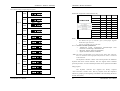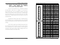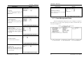
1
SYS7360V3EA
5.25” LITTLE BOARD Single Board Computer
For Intel® Ultra-Low Voltage Intel® Celeron® 400MHz
With VGA / Three LANs / Audio
User’s Manual
Ver. 0.91
Copyright
Copyright 2003 GRANTECH Co., Ltd. All Rights Reserved. No part
of this document may be copied or reproduced in any form by any
means without prior written consent of GRANTECH Co., Ltd.
GRANTECH Co., Ltd. makes no commitment to update or keep
current the information contained in this document. The information
in this document is subject to change without notice.
All relevant issues have been considered in the preparation of this
document. Should you notice an omission or any questionable item in
this document? Please feel free to notify GRANTECH Co., Ltd.
Regardless of the foregoing statement, GRANTECH assumes no
responsibility for any errors that may appear in this document nor for
results obtained by the user as a result of using this product.
Acknowledgments
IBM/AT and PS/2® are trademarks of International Business Machines
Corporation.
Award is a registered trademark of Award Software International, Inc.
Intel® CPU ULV Celeron® 400MHz is registered trademarks of Intel
Corporation.
Microsoft® Windows is a registered trademark of Microsoft
Corporation.
Limited One Year Warranty
GRANTECH Industrial CPU card is warranted by GRANTECH Co.,
Ltd. to be free from defects in material and workmanship for up to
one year from the date of purchase by the original purchaser.
Repair will be free of charge only when this device is returned
freight prepaid with a copy of the original invoice and a Return
Merchandise Authorization to the distributor or the GRANTECH
group office from which it was purchased.
This warranty is not applicable for scratches or normal wear, but
only for the electronic circuitry and original boards. The warranty is
not applicable if the device has been tampered with or damaged
through abuse, mistreatment, neglect, or unreasonable use, or if the
original invoice is not included, in which case repairs will be
considered beyond the warranty policy.
How to Obtain Service
For replacement or repair, return the device freight prepaid, with a
copy of the original invoice. Please obtain a Return Merchandise
Authorization Number (RMA) from our Sales Administration
Department before returning any product.
No product will be accepted by GRANTECH group without an
RMA number.
All Other product names or trademarks are properties of their
respective owners.
Caution about Battery
Liability
Danger of explosion if battery is incorrectly replaced.
The obligation of the warrantor is solely to repair or replace the
product. In no event will the warrantor be liable for any incidental or
consequential damages due to such defect or consequences that arise
from inexperienced usage, misuse, or malfunction of this device.
Replace only with the same or equivalent type recommended by the
manufacturer.
Dispose of used batteries according to the manufacturer’s
instructions.
Table of Contents
Table of Contents
Table of Contents
CHAPTER 1
INTRODUCTION ........................................................... 1
2.17
FRONT PANEL CONNECTOR: CN16...................................................22
2.18
EXTERNAL ATX CONTROL POWER CONNECTOR: CN17 ....................24
2.19
COMPACT FLASH CONNECTOR: CN18 ..............................................24
2.20
SYSTEM FAN CONNECTOR: FAN2...................................................25
1.1
SPECIFICATION................................................................................... 1
1.2
MECHANICAL & ENVIRONMENTAL ..................................................... 2
1.3
CHECK LIST ........................................................................................ 3
3.1
RS-422/485 TERMINATOR: JP1 .......................................................27
1.4
DESCRIPTION...................................................................................... 3
3.2
RS232/422/485 SELECTOR: JP2/JP3...............................................28
1.5
POWER MANAGEMENT FEATURES ...................................................... 4
3.3
PS/2® K/B & M/S JUMPERS: JP4/JP5/JP6/JP7错误!未定
1.6
POWER REQUIREMENTS...................................................................... 4
义书签。
1.7
CONNECTOR & JUMPER LOCATION..................................................... 6
3.4
ATX/AT POWER SUPPLY SELECT: JP8, JP17 ...................................31
1.8
BLOCK DIAGRAM ................................................................................ 7
3.5
CF MASTER / SLAVE SELECTOR: JP13 .............................................32
3.6
CLEAR CMOS CONTENT: JP16........................................................32
CHAPTER 2
CHAPTER 3
HARDWARE INSTALLATIONS ....................................... 8
CHAPTER 4
JUMPER SETTING ..................................................... 27
CPU CARD RESOURCES........................................... 33
2.1
INSTALLATION PROCEDURE ................................................................. 8
2.2
MAIN MEMORY INSTALLATION: DIMM1 ........................................... 9
4.1.
I/O MAP ..........................................................................................33
2.3
SERIAL PORT CONNECTOR: CN1 / CN7 ............................................ 10
4.2.
MEMORY MAP..............................................................................34
2.4
VGA CONNECTOR: CN2 .................................................................. 13
4.3.
DMA CHANNELS ..............................................................................34
2.5
RJ-45 LAN CONNECTOR: CN3 ........................................................ 14
4.4.
INTERRUPTERS..................................................................................34
2.6
PS/2 KEYBOARD/MOUSE CONNECTOR: CN4 .................................... 14
2.7
EXT. KEYBOARD CONNECTOR: CN5 .................错误!未定义书签。
2.8
USB CONNECTOR: CN6................................................................... 15
2.9
PARALLEL PORT CONNECTOR: CN8 ................................................. 16
2.10
FLOPPY DISK CONNECTOR: CN9...................................................... 18
2.11
LCD CONNECTOR: CN10................................................................. 19
2.12
EXTERNAL BATTERY CONNECTOR: CN11......................................... 20
2.13
AUDIO SIGNAL CONNECTOR: CN12 .................................................. 20
2.14
CD AUDIO CONNECTOR: CN13 ........................................................ 20
6.1.
INTRODUCTION .................................................................................42
2.15
EXTERNAL AT POWER CONNECTOR: CN14.......错误!未定义书签。
6.2.
MAIN MENU .....................................................................................44
2.16
PRIMARY IDE PORT CONNECTOR: CN15.......................................... 21
6.3.
STANDARD CMOS SETUP .................................................................46
SYS7360V3EA User’s Manual
i
CHAPTER 5
5.1.
VIA CLE266 VT8623/VT8235 CHIPSET DRIVER .............................36
5.2.
GRAPHIC DRIVER ..............................................................................38
5.3.
LAN DRIVER ....................................................................................38
5.4.
UPDATE NEW VERSION BIOS ............................................................39
5.5.
HARDWARE MONITOR .......................................................................40
CHAPTER 6
ii
SOFTWARE UTILITIES ............................................... 36
BIOS SETUP ........................................................... 42
SYS7360V3EA User’s Manual
Table of Contents
6.4.
ADVANCED BIOS FEATURES SETUP ................................................. 48
6.5.
ADVANCED CHIPSET FEATURES SETUP ............................................ 53
6.6.
INTEGRATED PERIPHERALS .............................................................. 61
6.7.
POWER MANAGEMENT SETUP........................................................... 68
6.8.
PNP/PCI CONFIGURATION SETUP .................................................... 74
6.9.
PC HEALTH STATUS ......................................................................... 77
6.10.
FREQUENCY/VOLTAGE CONTROL...................................................... 78
6.11.
DEFAULTS MENU ............................................................................. 79
6.12.
SUPERVISOR/USER PASSWORD SETTING ........................................... 79
6.13.
EXIT SELECTING............................................................................... 80
6.14.
POST CODES ................................................................................... 81
SYS7360V3EA User’s Manual
iii
Table of Contents
iv
SYS7360V3EA User’s Manual
CHAPTER 1 –Introduction
CHAPTER 1 –Introduction
Hardware Monitor:.
Chapter 1 Introduction
1.1
®
Keyboard connector: One PS/2 keyboard connector on bracket and
share with mouse and one 6-pins box-header for external
keyboard.
Specification
®
Mouse connector: On bracket PS/2 Mouse connector share with
keyboard.
Processor:
VGA Controller: Integrate VT8623 frame buffer share with system
memory.
SYS7360V3EA: Ultra-Low Voltage Intel® Celeron® Processor (0.13u)
in the Micro FC-BGA package 400MHz, FSB
100MHz at CPU core voltage 0.95V.
VGA Connector: On board 15-pin D-type VGA connector.
Form Factor: 5.25” little board single card.
LCD: 40 pin TFT LCD panel digital signal connector.
Chipset: VIA CLE266 Chipset (VT8623) + (VT8235).
LAN: Three Realtek RT8139D controllers, three RJ-45 connector on
board.
Cache Size: On-die primary 16-Kbyte instruction cache and
16-Kbyte write –back data cache and on-die second level cache
(256-Kbyte for the ULV Celeron® Processor 400MHz) with
advanced transfer cache architecture.
Wake On LAN support, Remote Boot-up
RTC: battery backup by Lithium Battery (CR2032/BR2032)
Memory: Up to 512MB DDR SDRAM (PC-100) DIMM.
The coin type Lithium battery specification is shown in
Memory Sockets: One 184-pin DDR SDRAM socket for SDRAM in
64MB, 128MB, 256MB and 512MB configurations.
table
Specification
CR2032
BR2032
Nominal Voltage
3V
3V
Nominal Capacity
220mAh
195mAh
Nominal Weight
3.1g
2.4g
* The maximum using duration of CR2032/BR2032 Battery is about
3 years at 20oC.
BIOS: Award BIOS, PnP support
Flash EEPROM (256KB) for BIOS update
Power management
LPC Super I/O: Winbond W83697UF.
1.2
Parallel port: One high-speed parallel port, SPP/EPP/ECP mode
Series Port: Four 16550 UART ports, COM2 is RS-232/422/485
configurable.
Mechanical & Environmental
POWER CONSUMPTION (Intel ULV Celeron 400 MHz) :
Enhanced IDE: One EIDE port, up to 2 IDE devices, supports Ultra
DMA 33/66/100/133.
Compact Flash: One CF port support memory card.
♦
+5VDC @ 5.372A max.
♦
+12VDC @ 0.50A max.
♦
+5VSB @ 1.924A max.
FDD Interface: One floppy drives (360KB, 720KB, 1.2MB, 1.44MB,
2.88MB, LS-120)
OPTERATING TEMPERATURE: 0 ~ 55℃.
USB Interface: One box-header support 2 USB v2.0 ports
STORAGE TEMPPERATURE: - 40 ~ 80℃.
Watchdog Timer: Supper I/O integrate WDT timer and Software
programmable active to Reset.
HUMIDITY: 20% to 90% RH (no condensation)
Board dimension: 203mm(L) X 146mm(W) / 8”inch X 5.75” inch.
SYS7360V3EA User’s Manual
1
2
SYS7360V3EA User’s Manual
CHAPTER 1 –Introduction
CHAPTER 1 –Introduction
BOARD WEIGHT: 300 g.
1.3
1.5
Check List
Power Management Features
Overview
Support both ACPI (Advanced Configuration and Power Interface)
and legacy (APM) power management
Please check that your package is complete and contains the items below. If
you discover damaged or missing items, please contact your dealer.
ACPI v1.0 compliant
The SYS7360V3EA Industrial PCI CPU board
APM v1.2 compliant
This User’s Manual & Registration Card
CPU clock throttling and clock stop control for complete ACPI C0
to C1.
1 IDE 80pin Ribbon Cables
1 Floppy Ribbon Cable
Driver disks utilities
PCI bus clock run, Power Management Enable (PME) control, all
with hardware automatic wake-up
One mounting bracket attached with 1 serial ports & 1 parallel
port ribbon cable
Multiple suspend power plane controls and suspend status indicators
Jumper Short Pin: 15 pcs of pitch 2.0 mm, and 2 pcs of pitch 2.54
mm.
One idle timer, one peripheral timer and one general purpose timer,
plus 24/32-bit ACPI compliant timer
®
6 pin mini-DIN cable (2 in 1 cable for PS/2 Mouse & Keyboard
function)
Normal, doze, sleep, suspend and conserve modes
Global and local device power control
1.4
Description
System event monitoring with two event classes
Primary interrupt differentiation for individual channels
The SYS7360V3EA is a PCI compatible Industrial CPU card based on
VIA VT8623/VT8235 chipset and is fully designed for harsh industrial
1.6
environment. It features Intel® ULV μFC-BGA series compatible processor.
This card accommodates up to 512MB of DDR SDRAM memory.
Power Requirements
Your system requires a clean, steady power source for reliable
The SYS7360V3EA comes with CPU integrate temperature sensor to
performance of the high frequency CPU on the SYS7360V3EA Industrial CPU
protect your processor from overheating; and wired for Management (WFM)
card, the quality of the power supply is even more important. For the best
2.0 specifications compliance.
performance makes sure your power supply provides a range of 4.75 volts
The SYS7360V3EA has three LAN connectors that use Realtek’s
RT8139D PCI LAN controller.
minimum to 5.25 volts maximum DC power source.
Power Consumption
The SYS7360V3EA has a LCD connector that uses VT8623 integrate
For typical configurations, the CPU card is designed to operate with at
graphic accelerator.
least a 200 W power supply. A higher-wattage power supply should be used for
heavily-loaded configurations. The power supply must meet the following
SYS7360V3EA User’s Manual
3
4
SYS7360V3EA User’s Manual
CHAPTER 1 –Introduction
CHAPTER 1 –Introduction
requirements:
1.7
Connector & Jumper Location
Rise time for power supply: 2 ms to 20 ms
ML5-71-E3VA M065
Minimum delay for reset to Power Good: 100 ms
CN21
DIMM 1
CN11
Minimum Power down warning: 1 ms
CN22
3.3 V output must reach its minimum regulation level within 20ms of the
CN9
+5V output reaching its minimum regulation level
( SOLDER SIDE )
ULV CPU
The following table lists the power supply’s tolerances for DC voltages:
CN8
JP8
DC Voltage
+3.3 V
+5 V
+5 VSB (standby)
+12 V
Acceptable Tolerance
±5%
±5%
±5%
±5%
SLOT1
CN19
CN20
CN33
JP19
JP15
JP23
JP24
CN28
CN29
CN5
CN12
JP21
JP20
JP16
JP17
JP1
JP2
JP22
IR1
CN14
CN15
FAN2
JP13
CN23
JP14
CN34
CN24
JP7
CN4
CN32
CN2
SYS7360V3EA User’s Manual
5
6
CN6
CN7
JP18
CN26
SYS7360V3EA User’s Manual
CHAPTER 1 –Introduction
1.8
CHAPTER 2 –Hardware Installations
Chapter 2 Hardware Installations
Board layout and dimensions
This chapter provides information on how to use the jumpers and
connectors on the SYS7360V3EA in order to set up a workable system.
2.1
Installation procedure
2.1.1 Insert the DDR DRAM module with correct orientation.
2.1.2 Insert all external cables except for flat panel. (Hard disk, floppy,
keyboard, Mouse, LAN, etc.)
2.1.3 Prepare a CRT monitor for CMOS setup.
2.1.4 Confirm CPU card into to PCI back plane.
2.1.5 Turn on the power.
2.1.6 Enter the BIOS setup mode by pressing ‘Del’ key during boot up.
2.1.7 Use the “Load BIOS Optimal Defaults” feature.
2.1.8 Configure the Peripheral Setup and the Standard Setup correctly.
Note: The CMOS memory may be in an undefined state at power-on after a
period of no battery backup.
SYS7360V3EA User’s Manual
7
8
SYS7360V3EA User’s Manual
CHAPTER 2 –Hardware Installations
CHAPTER 2 –Hardware Installations
Note: All memory components and DIMM used with the SYS7360V3EA PCI
2.2
Main Memory Installation: DIMM1
CPU card must comply with the PC SDRAM Specification. These include: the
The SYS7360V3EA PCI Industrial CPU Card supports one dual inline
memory module (DDR SDRAM DIMM 184-pin) socket for a maximum total
PC SDRAM Specification *memory component specific) , the PC Un-buffered
DIMM Specification, and the PC Serial Presence Detect Specification.
memory of 512MB on PC100. Using the serial presence detect (SPD) data
2.3
structure, programmed into an E2PROM on the module, the BIOS can determine
the size of SDRAM and speed. Minimum memory size is 64MB; maximum
memory size is 512MB. Memory size and speed can vary between sockets.
The CPU card supports the following memory features:
•
184-pin DDR SDRAM DIMM with gold-plated contacts
•
100 or 133 MHz DDR SDRAM.
•
Non-ECC function support.
•
2.5V memory only.
•
Un-buffer single or double-sided DIMM in the following sizes:
Serial Port connector: CN34 (COM1~COM4)
COM1~COM4 (CN34) is a 40-pins box-header; cable with D-sub
connector . The following table shows the pin assignments of these connectors.
** 4 serial ports on board supports with-out ISA bridge( PC/104)
model only
The CN34 pin assignment:
PIN
PIN
PIN
PIN
RS-232
1
11
21
31
DCD
2
12
22
32
DSR
3
13
23
33
SIN
4
14
24
34
RTS
5
15
25
35
SOUT
through memory access that is synchronous with the memory clock. Burst
6
16
26
36
CTS
transfer rates at x-1-1-1 timing can be achieved using SDRAM, while
7
17
27
37
DTR
8
18
28
38
RIN
9
19
29
39
GND
10
20
30
40
N.C
CN34
1
2
SDRAM
SYNCHRONOUS DRAM (SDRAM) improves memory performance
asynchronous memory subsystems are typically limited at x-2-2-2 transfer rates.
39
The CPU card supports single or double-sided DIMM in the following
sizes:
DIMM size
64MB
128MB
256MB
512MB
SYS7360V3EA User’s Manual
Non-ECC configuration
8Mbit x 64
16Mbit x 64
32Mbit x 64
64Mbit x 64
9
10
40
SYS7360V3EA User’s Manual
CHAPTER 2 –Hardware Installations
CHAPTER 2 –Hardware Installations
Pin 8,18,28.38 ring-in signal & power option
JP15
JP16
COM1
1
2
1
JP19
2
RS422/485 assigned for COM2 connector only
3
JP17
COM2
1
Ring-in
2
1
JP23
2
COM2 D-SUB
3
JP20
COM3
1
2
1
JP24
2
3
JP21
COM4
1
2
1
JP15
2
3
JP16
COM1
1
2
1
JP19
2
+5V
1
JP23
2
1
JP20
2
1
2
3
JP21
COM4
1
2
1
JP15
2
2
1
2
3
JP17
TX-
TX-
RXD
TX+
TX+
3
TSD
RX+
RX+
4
DTR
RX-
RX-
5
GND
GND
GND
6
DST
RTS-
N.C
7
RTS
RTS+
N.C
8
CTS
CTS+
N.C
9
RI
CTS-
N.C
10
N.C
N.C
N.C
The keyboard controller contains code which provides the traditional
COM2
keyboard and mouse control functions, and also supports Power On/Reset
1
+12V
DCD
2
Note: The mouse and keyboard can be plugged into either PS/2 connector.
Power to should be turned off before a keyboard or mouse is connected
or disconnected.
COM1
1
1
3
JP16
JP19
RS485
For RS-485, TX+(pin 2) and RX+ (pin 3) must jumper together
inside the D type connector.
TX- (pin 1) and RX- (pin 4) is the same.
2.3.1 RS-422 / RS-485 specifications
Transmission system: Asynchronous, half-/full-duplex serial
transmission conforming to RS-422/RS-485
Baud rate: 19200 to 50bpx (programmable)
Signal extensible distance: 1.2km Max.
3
COM3
JP24
RS422
Note:
JP17
2
RS-232
3
COM2
1
PIN
2
1
JP23
2
3
password protection. A Power On/Reset password can be specified in the BIOS
JP20
Setup program.
COM3
1
2
1
JP24
2
3
The
JP21
COM4
keyboard
controller
also
supports
the
hot-key
sequence
<Ctrl><Alt><Del>, software reset. This key sequence resets the computer’s
1
2
1
2
3
software by jumping to the beginning of the BIOS code and running the Power
On Self Test (POST).
SYS7360V3EA User’s Manual
11
12
SYS7360V3EA User’s Manual
CHAPTER 2 –Hardware Installations
2.4
CHAPTER 2 –Hardware Installations
TV_OUT :CN26
2.6
The Video port function by RCA Video or S/SPDIF
assignments are as follows
RJ-45 LAN connector: CN4,CN6,CN7
The pin
These connectors are for the 10/100Mbps Ethernet capability of the CPU
card. The follow table shows the pin assignments of these connectors.
CN26
Function
2
1
TV_OUT
2
TV_GND
The category-5 cable is required for transmission at 100Mbps.
1
1
2.5
2
3
L in k & A C T
LED
VGA Connector: CN2
2.7
It is a VGA CRT connector (DB-15). The pin assignments are as follows:
4
5
6
7
PIN No.
1
2
3
4
5
6
7
8
8
1 0 0 D e te c t
LED
Function
TX+
TXN.C
AGND
AGND
BYPASS
RX+
RX-
PS/2 Keyboard/Mouse Connector: CN12
The CPU board provides a 6pins box-header connector for attaching
CN2
1
PIN No. Function PIN No.
1
9
RED
2
10
GREEN
3
11
BLUE
4
12
N.C
5
13
GND
6
14
GND
7
15
GND
8
GND
Function
N.C
GND
D-DATE
N.C
H-SYNC
V-SYNC
D-DCLK
the PS/2® mouse or keyboard. The Connector pin definition is shown below:
1
6
PIN No.
Function
1
+5VSB
2
MS Clock
3
MS Data
4
KB Clock
5
KB Data
6
GND
When used with an ATX-compliant power supply that supports remote
power on/off, the CPU card can turn off the system power through software
control.
To enable soft-off control in software, advanced power management
must be enabled in the Setup program and in the operation system. When the
system BIOS receives the correct APM command from the operating system, the
SYS7360V3EA User’s Manual
13
14
SYS7360V3EA User’s Manual
CHAPTER 2 –Hardware Installations
CHAPTER 2 –Hardware Installations
Guaranteed bandwidth and low latencies appropriate for telephony, audio
BIOS turns off power to the computer.
and other applications
With soft-off enabled, if power to the computer is interrupted by a power
Error-handling and fault-recovery mechanisms built into the protocol
outage or a disconnected power cord, when power resumes, the computer returns
Note: Computer systems that have an unshielded cable attached to a USB port
to the power state it was in before power was interrupted (on or off) .
may not meet FCC Class A requirements, even if no device or a low-speed USB
2.8
USB Connector: CN32,CN33.CN5
device is attached to the cable. Use shielded cable that meets the requirements
The Universal Serial Bus (USB) that allows plug and play computer
for full-speed devices.
peripherals such as legacy keyboard, PS/2 mouse, scanner, printer, modem/ISDN,
PIN No.
and floppy disk drive to be automatically detected when they are attached
1
physically without having to install drivers or reboot.
The USB connectors allow any of several USB devices to be attached to
the computer. Typically, the device driver for USB devices is managed by the
CN5
Function
PIN No.
CN33
Function
1
5VSB
1
5VSB
2
USBD2-
2
USBD4-
3
USBD2+
3
USBD4+
4
USBD3-
4
USBD5-
needed in the Setup program before the operating system boots, the BIOS
5
USBD3+
5
USBD5+
support USB keyboards
6
GND
6
GND
operating system. However, because keyboard and mouse support may be
6
The CPU card has three USB ports; one USB peripheral can be
connected to each port. For more than two USB devices, an external hub can be
connected to either port. The two USB ports are implemented with stacked back
PIN No.
panel connectors. The CPU card fully supports the universal host controller
interface (UHCI) v1.1 compatible and uses enhanced host controller interface
5
8
(EHCI) v1.0 compatible software drivers and USBv2.0.
USB features includes:
1
Self-identifying peripherals that can be plugged in while the computer is
4
CN32
Function
PIN No.
CN32
Function
1
5VSB
5
5VSB
2
USBD0-
6
USBD1-
3
USBD0+
7
USBD1+
4
GND -
8
GND -
running
Automatic mapping of function to driver and configuration
Support for synchronous and asynchronous transfer types over the same set
of wires
Support three root hubs and six function ports.
SYS7360V3EA User’s Manual
15
16
SYS7360V3EA User’s Manual
CHAPTER 2 –Hardware Installations
2.9
CHAPTER 2 –Hardware Installations
2.10 Floppy Disk Connector: CN14
Parallel Port Connector: CN15
The floppy interface can be configured for the following floppy drive
The parallel port bracket can used to add an additional parallel port for
additional parallel devices. There are four options for parallel port operation:
capacities and sizes:
360 KB, 5.25-inch
Compatible (Standard mode)
1.2 MB, 5.25-inch
Bi-Directional (PS/2 compatible)
720 KB, 3.5-inch
Bi-Directional EPP. A driver from the peripheral manufacturer is
1.44 MB, 3.5-inch
required for operation.
Bi-Directional High-speed ECP
PIN
Function
No.
CN15
1
STROBE
3
PD0
1
2
5
PD1
7
PD2
9
PD3
11
PD4
13
PD5
15
PD6
17
PD7
19
ACK
21
BUSY
25
26
23
PE
25
SLCT
2.88 MB, 3.5-inch
PIN
No.
2
4
6
8
10
12
14
16
18
20
22
24
26
This connector supports the provided floppy drive ribbon cable. After
Function
connecting the single and to the board, connect the two plugs on the other end
ALF
ERROR
INIT
SLCT IN
GND
GND
GND
GND
GND
GND
GND
GND
N.C
to the floppy drives.
CN14
1
33
SYS7360V3EA User’s Manual
17
18
2
34
PIN No.
1
3
5
7
9
11
13
15
17
19
21
23
25
27
29
31
33
Function
GND
GND
GND
GND
GND
GND
GND
GND
GND
GND
GND
GND
GND
GND
GND
GND
GND
PIN No.
2
4
6
8
10
12
14
16
18
20
22
24
26
28
30
32
34
Function
RWC
N.C
N.C
INDEX
DS0
DS1
DS2
MOT ON
DIR
STEP
WD
WG
TRCK 0
WP
RD
SIDE 1
DSK CHG
SYS7360V3EA User’s Manual
CHAPTER 2 –Hardware Installations
CHAPTER 2 –Hardware Installations
2.12 External Battery Connector: CN1
2.11 LCD Connector: CN19
It is a 2 Pin connector used for external battery. An external battery
CN10 is a 40-pin connector (Panel link) for flat panel LCD display. The
power for used of real-time clock and CMOS memory.
following shows the pin assignment of this connector.
CN11
PIN No.
1
3
5
7
9
11
13
15
17
19
21
23
25
27
29
31
33
35
37
39
Function
DP20
DP16
DP21
DP17
DP22
DP18
DP23
DP19
VCC
FLM
MX
LP
GND
SHFCLK
3.3V
3.3V
ENABLK
LCDVDD
ENVEE
GND
SYS7360V3EA User’s Manual
PIN No.
2
4
6
8
10
12
14
16
18
20
22
24
26
28
30
32
34
36
38
40
Function
GND
VCC
DP0
DP8
DP1
DP9
DP2
DP10
DP3
DP11
DP4
DP12
DP5
DP13
DP6
DP14
DP7
DP15
+12V
+12V
PIN
No.
Function
1
GND
2
External
battery (3V)
2.13 Audio Signal connector: CN23
PIN No.
CN23
1
9
2
10
1
3
5
7
9
Function
LINE-OUT
-R
GND
NC
GND
LINE-IN-R
PIN No.
2
4
6
8
10
Function
LINE-OUT
-L
GND
MICIN
GND
LINE-IN-L
2.14 CD Audio connector: CN24
This connector is used to connect CD Audio cable from CD-ROM or
DVD drive to onboard sound.
CN24
1 2 3 4
19
20
PIN No.
Function
1
Audio-L
2
GND
3
GND
4
Audio-R
SYS7360V3EA User’s Manual
CHAPTER 2 –Hardware Installations
CHAPTER 2 –Hardware Installations
2.15 Primary /Seconadry IDE port Connector:
CN22 ( 2x40 2.54mm Box Header)/
CN11( 2x22 2.0mm Box Header)
CN22
1
2
39
40
The CPU card SYS7360V3EA has two independent bus-mastering
PCI IDE interfaces. Transfer rate up to 133MB/sec to cover PIO mode 4,
multi-word DMA mode 2 drivers, and UltraDMA133 interface, and increased
reliability using Ultra DMA-133/100/66 transfer protocols. The BIOS supports
logical block addressing (LBA) and extended cylinder head sector (ECHS)
translation modes. The BIOS automatically detects the IDE device transfer rate
and translation mode.
Programmed I/O operations usually require a substantial amount of
processor bandwidth. However, in multitasking operating systems, the bandwidth
CN11
freed by bus mastering IDE can be devoted to other tasks while disk transfers are
occurring.
1
2
These connectors support the provided IDE hard disk ribbon cable.
After connecting the single end to the board, connect the two plugs at the other
end to your hard disk(s). If you install two hard disks, you must configure the
second drive to Slave mode by setting its jumper accordingly. Please refer to
your hard disk documentation for the jumper setting.
43
SYS7360V3EA User’s Manual
21
22
44
PIN No.
1
3
5
7
9
11
13
15
17
19
21
23
25
27
29
31
33
35
37
39
Function
RESET
D7
D6
D5
D4
D3
D2
D1
D0
GND
DREQ
IOW
IOR
IORDY
DACK
IRQ
A1
A0
CS0
HD ACT
PIN No.
1
3
5
7
9
11
13
15
17
19
21
23
25
27
29
31
33
35
37
39
41
43
Function
RESET
D7
D6
D5
D4
D3
D2
D1
D0
GND
DREQ
IOW
IOR
IORDY
DACK
IRQ
A1
A0
CS0
HD ACT
VCC
GND
PIN No.
2
4
6
8
10
12
14
16
18
20
22
24
26
28
30
32
34
36
38
40
Function
GND
D8
D9
D10
D11
D12
D13
D14
D15
N.C
GND
GND
GND
ALE
GND
IOCS16
PDIAG
A2
CS1
GND
PIN No.
2
4
6
8
10
12
14
16
18
20
22
24
26
28
30
32
34
36
38
40
42
44
Function
GND
D8
D9
D10
D11
D12
D13
D14
D15
N.C
GND
GND
GND
ALE
GND
IOCS16
PDIAG
A2
CS1
GND
VCC
NC
SYS7360V3EA User’s Manual
CHAPTER 2 –Hardware Installations
CHAPTER 2 –Hardware Installations
2.16 Front Panel Connector: CN21
This header can be connected to a front panel power switch. The front
panel connector includes headers for these I/O connections:
Power / Suspend LED
This header can be connected to an LED that will light when the
computer is powered on and LED flash when OS into standby mode.
HDD LED
This header can be connected to an LED to provide a visual indicator
that data is being read from or written to an IDE hard drive. For the LED to
2.17 External ATX control Power Connector:
CN22
function properly, the LED drive must be connected to the onboard IDE
controller.
Speaker
A external speaker can be installed on the SYS7360V3EA as a
CN22
manufacturing option. The external speaker enabled by connect 4 pin hosing
connector to external speaker on pins 9, 11, 13, 15 of the front panel connector.
3
2
1
The onboard speaker can be removed by mounting optional, and an off board
speaker can be connected in its place. The speaker (onboard or off board)
provides error beep code information during the POST in the event that the
computer cannot use the video interface.
PIN No. Sign name PIN No. Sign name
CN21
1
2
Power BT
VCC
3
4
GND
IDE ACT
1
2
3
4
5
6
RESET
NC
5
6
7
8
GND
VCC
7
8
9
10
9
10
VCC
VCC
11
12
11
12
GND
For GPO0
13
14
13
14
15
16
GND
NC
15
16
BUZZER
NC
Speaker
Power Button
9, 11, 13, 15
1, 3
Reset Button
HDD LED
5, 7
2, 4
Power LED
10, 12
SYS7360V3EA User’s Manual
23
PIN No.
Function
Housing:
3
5V SBY
XHP-3 (JST)
2
PS-ON (soft ON/OFF)
1
GND
2.18 Compact Flash Connector: CN9
The CPU card SYS7360V3EA provides a Compact lash interfaces.
This interface is a very small removable mass storage device. It provides
compatibility plus True IDE functionality compatible with ATA/ATA-4.
24
SYS7360V3EA User’s Manual
CHAPTER 2 –Hardware Installations
CN9
1
2
49
50
PIN
No.
1
3
5
7
9
11
13
15
17
19
21
23
25
27
29
31
33
35
37
39
41
43
45
47
49
Function
GND
D4
D6
CS0
ATASEL#
A082
VCC
A052
A032
A01
D0
D2
CD2#
D111
D131
D151
VS1#
IOW
INTQ
CSEL#
RESET
INPACK
DASP#
D081
D101
PIN
No.
2
4
6
8
10
12
14
16
18
20
22
24
26
28
30
32
34
36
38
40
42
44
46
48
50
Function
CN27 GPIO PORT 2X5 2.0mm Pin Header
D3
D5
D7
A102
A092
A072
A062
A042
A02
A00
D1
IOCS16
CD1#
D121
D141
CS11
IOR
WE3#
VCC
VS2
IORDY
REG3#
PDIAG
D091
GND
TTL level bi-directional pin ,internal pull Hi +5V
CN27
1
3
5
7
9
1
2
Function
1
GND
2
+12V
3
FAN sense
SYS7360V3EA User’s Manual
Sign name
PIN No.
Sign name
1
DI-0
2
DO-0
3
DI-1
4
DO-1
5
DI-2
6
DO-2
7
DI-3
8
DO-3
GND
10
GND
2
4
6
8
10
Smbus ID = 30h
Smbus Port = 5000h
GPI24 connect GPO12
GPI23 connect GPO13
GPI11 connect GPO14
GPI10 connect GPO15
Program GPIO Function:
1. Input/Output Configuration Register setting.
2. Polarity Inversion Register setting.
3. Send Output port Data or Check Input port Data.
FAN2 is a 3-pins box-header for the system cooling fan power connector.
The fan must be a 12V fan. Pin 3 is for Fan speed sensor input. Pin 2 is for +12V
power supply.
PIN No.
PIN No.
9
2.19 System FAN Connector: FAN2
FAN2
CHAPTER 2 –Hardware Installations
Connector type for Cable
Housing: 5102-03 (molex)
Contact: 5103 (molex)
Program Smbus Write:
1. Check Smbus Busy
2. Set Smbus Port + 4 = ID (30h)
3. Set Smbus Port + 3 = Inedx
4. Set Smbus Port + 5 = Write Date
5. Set Smbus Port + 2 = Write Command(48h)
Program Smbus Read:
1. Check Smbus Busy
2. Set Smbus Port + 4 = ID (31h)
3. Set Smbus Port + 3 = Inedx
4. Set Smbus Port + 2 = Write Command(48h)
5. Get Date = Smbus Port + 5
25
26
SYS7360V3EA User’s Manual
CHAPTER 3 –Jumper Setting
CHAPTER 3 –Jumper Setting
3.2
Chapter 3 Jumper Setting
RS232/422/485 Selector: JP14/JP18
JP14
3.1
RS-422/485 Terminator: JP13
JP18
2
4
6
8
10
12
14
16
18
20
1
3
5
7
9
11
13
15 17 19
2
4
6
8
10
12
14
16
1
3
5
7
9
11
13
15 17 19
2
4
6
8
10
12
14
16
1
3
5
7
9
11
13
15 17 19
22
24
2
4
6
8
10
1
3
5
7
9
2
4
6
8
10
1
3
5
7
9
2
4
6
8
10
1
3
5
7
9
RS-232
JP13
Terminator
Function
21
23
JP13
1
3
5
7
2
4
6
8
-
No terminating resister
(Default)
JP14
JP18
18
20
22
24
RS-422
JP13
1
3
5
7
2
4
6
8
CTS for RS-422
2
4
6
8
23
JP14
JP13
1
3
5
7
21
terminating resister provided
RTS for RS-422
JP18
18
20
22
24
RS-485
terminating resister provided
21
23
JP13
1
3
5
7
2
4
6
8
RXD for RS-422/485 terminating resister provided
2
4
6
8
TXD for RS-422/485
1. For RS-485, TX+(pin 2) and RX+ (pin 3) must jumper together
inside the D type connector.
2. TX- (pin 1) and RX- (pin 4) is the same.
JP13
1
3
5
7
SYS7360V3EA User’s Manual
terminating resister provided
27
28
SYS7360V3EA User’s Manual
CHAPTER 3 –Jumper Setting
CHAPTER 3 –Jumper Setting
3.2.2
Transmit date control in half-duplex mode
RS-485 Setting
RTS#
In half-duplex mode, the transmission buffer must be controlled to prevent
JP18:7-8
CN34
11
transmit data from causing a collision. The SIS-8600-LV uses the RTS signal
TXD#
and bit 1 in the modem control register to control transmit data.
D
120 OHM
JP13:7-8
12
JP18:4-6
Modem control register
DATADATA+
13
RXD#
(Setting I/O address +4H) bit 1: 0 … RTS High (Disables transmission)
R
120 OHM
JP13:5-6
14
JP18:5-6
1 … RTS low (Enables transmission)
Setting the RS-422/RS-485 receiver disable control jumper
When the RS-422/RS-485 port is used, the RTS signal is used for driver
enable control Connecting JP1 Pins 4 and 6 disables the receiver at the same
time, preventing the port from receiving output data to an external device.
3.2.1
I/O addresses and instructions
RS-422 Setting
The table below lists I/O addresses for use as COM2.
RTS#
I/O address
JP18:7-8
DLAB
CN34
11
TXD#
D
120 OHM
JP13:7-8
JP18:4-6
Transmitter holding Register
THR
R
Receiver buffer Register
RBR
1
W
Divisor latch Register (LSB)
DLL
02F8H
13
RXD#
R
120 OHM
JP13:5-6
14
JP18:5-6
RTS
D
CTS
120 OHM
JP13:3-4
1
W
Divisor latch Register (MSB)
DLM
15
02F9H
0
W
Interrupt enable Register
IER
16
02FAH
X
R
Interrupt ID Register
IIR
02FBH
X
W
Line control Register
LCR
02FCH
X
W
Modem Control Register
MCR
02FDH
X
R
Line status Register
LSR
02FEH
X
R
Modem Status Register
MSR
02FFH
X
R/W
Scratch Register
SCR
17
R
120 OHM
JP13:1-2
18
JP19
+12V
+5V
JP17
SYS7360V3EA User’s Manual
Register
W
0
12
Read/Writ
e
29
30
SYS7360V3EA User’s Manual
CHAPTER 3 –Jumper Setting
CHAPTER 3 –Jumper Setting
3.4
CF Master / Slave selector: JP8
JP8
3.3
ATX/AT Power supply select: JP1, JP22
JP8
In case for different type of power supply, the user needs setting up
these jumpers for more system stability.
JP8
JP1
JP22
JP8
JP17
Set to Master
Set to Slave
Function
3.5
ATX
1
2
3
JP8
1
2
2
The CMOS values can be returned to their defaults by using the Setup program.
JP17
3
1
2
Clear CMOS Content: JP2
The time, date, and CMOS values can be specified in the Setup program.
3
AT
1
Function
The RAM data contains the password information is powered by the onboard
3
button cell battery. User can erase the CMOS memory content by short pin2 and
pin3 of JP16 together.
An external coin-cell battery powers the real-time clock and CMOS
memory. When the computer is not plugged into a wall socket, the battery has an
estimated life of eight years. When the computer is plugged in, the 3.3 V standby
current from the power supply extends the life of the battery. The clock is accurate
to ± 1 minutes/month at 25ºC with 3.3V applied.
JP2
Function
JP2
Normal Operation (Default)
1
2
3
JP2
Clear CMOS Content
1
SYS7360V3EA User’s Manual
31
32
2
3
SYS7360V3EA User’s Manual
CHAPTER 4 – CPU Card Resources
CHAPTER 4 –CPU Card Resources
4.2. MEMORY MAP
Chapter 4 CPU card Resources
4.1. I/O MAP
Address (hex)
Description
Address Range
(H)
Size
100000-18000000
383MB
Description
Extended memory
00-1F
DMA Controller
E8000-FFFFF
96KB
System BIOS
20-3F
Interrupt Control (PIC)
E0000-E7FFF
32KB
System BIOS (Available as UMB)
40-5F
Timer / Counter
C8000-DFFFF
96KB
(60h)
KBC Data
Available high DOS memory (open to ISA
and PCI buses)
(61h)
Misc Function & Speaker Ctrl
A0000-C7FFF
160KB
Video memory and BIOS
(64h)
KBC Command / Status
00000-9FFFF
640KB
Conventional memory
70-77
RTC/CMOS/NMI-Disable
78-7F
-available for system use-
80
4.3. DMA Channels
-reserved- (debug port)
DMA
Data Width
System Resources
81-8F
DMA Page Registers
0
8 or 16bits
Audio
90-91
-available for system use-
1
8 or 16bits
Audio / parallel port
2
8 or 16bits
Diskette drive
3
8 or 16bits
Parallel port (for ECP) /audio
92
System Control
93-9F
-available for system use-
A0-BF
Slave Interrupt Controller
5
16bits
Open
C0-DF
Slave DMA Controller
6
16bits
Open
E0-FF
-available for system use-
7
16bits
Open
100-CF7
-available for system use-
CF8-CFB
PCI Configuration Address
CFC-CFF
PCI Configuration Data
D00-FFFF
-available for system use-
SYS7360V3EA User’s Manual
4
Reserved – cascade channel
4.4. Interrupters
IRQ #
NMI
33
34
System Resources
I/O Channel check
0
Reserved, interval timer
1
Reserved, keyboard controller
2
Reserved, cascade interrupt from slave PIC
3
COM2*
4
COM1*
SYS7360V3EA User’s Manual
CHAPTER 4 – CPU Card Resources
IRQ #
Chapter 5 Software Utilities
System Resources
5
LPT2 (Plug and Play option) /audio/user available
6
Diskette drive controller
7
LPT1*
8
Real time clock
CLE266 VT8623/VT8235 chipset VIA Service Pack (VIA 4 In 1) / Graphics
9
User available
drivers for CRT/Flat Panel Driver and watchdog function configuration utility.
10
USB/User available
11
Windows Sound System/User available
12
PS/2 mouse port (if present, else user available)
13
Reserved, math coprocessor
14
Primary IDE (if present, else user available)
15
•
CHAPTER 5 – Software Utilities
This
chapter
introduces
the
software
utilities
supplied
for
SYS7360V3EA which including a 10/100M Ethernet driver, VIA Apollo
5.1. VIA CLE266 VT8623/VT8235 chipset Driver
VIA Service Pack (VIA 4 In 1)
VIA Service Pack (VIA 4 In 1) is Copyright(C) 1999 VIA Technologies, Inc.
Secondary IDE (if present, else user available)
Table of Contents:
* Default, but can be changed to another IRQ
About VIA 4 In 1
Setting Up
Update
Technical Support
Special Note (WinFast AGP VGA users only)
About VIA 4 In 1:
VIA 4 In 1 driver includes four system drivers to improve the
performance and maintain the stability of systems using VIA chipsets. These
four drivers are:
VIA Registry (INF) Driver
VIA AGP VxD driver, VIA ATAPI Vendor Support Driver
VIA PCI IRQ Mini port Driver. For Windows NT users
VIA IDE Bus Mastering driver is the only driver to be installed in
your system.
VIA Registry (INF) Driver is to be installed under Windows. The driver will
enable the VIA Power Management function.
VIA AGP VxD Driver is to be installed if you are using an AGP VGA device.
SYS7360V3EA User’s Manual
35
36
SYS7360V3EA User’s Manual
CHAPTER 5 – Software Utilities
CHAPTER 5 – Software Utilities
VIA PCI IRQ Miniport Driver
VIAGART.VXD will provide service routines to your VGA driver and interface
directly to hardware, providing fast graphical access.
The ATAPI IDE driver enables the performance enhancing bus mastering
functions on ATA-capable Hard Disk Drives and ensures IDE device
compatibility.
VIA PCI IRQ Mini port Driver is to be installed under Windows 98 only, it sets
the system's PCI IRQ routing sequence.
Install, Uninstall
Step 5: Reboot system to complete driver setup process
5.2. Graphic Driver
Introduction
Setting Up:
The CPU card SYS7360V3EA is integrated VGA controller for VGA / LCD
You may Install and Uninstall VIA driver by selecting the proper
options.
designs.
Driver Support
Step 1: To setup the driver, double click the "SETUP.EXE" icon or run
"SETUP.EXE" under VIA 4 In 1 Driver directory.
Step 2: Bypass the "Welcome" dialog by clicking "Next"
Step 3: In "Select Component" dialog, choose driver(s) you wish to install by
clicking the check box of each driver. Selected driver(s) will display
tick(s) . After selecting proper driver(s) , click next
Step 4: Driver options select
•
Windows 95
•
Windows 98
•
Windows NT4.0
•
Windows 2000
•
Windows XP
5.3. LAN Driver
VIA ATAPI Vendor Support Driver dialog:
Introduction
Install
Uninstall
The CPU card SYS7360V3EA is adopted the Realtek RTL8139D for PCI bus
Enable/Disable DMA Mode
LAN designs.
The LAN DRIVER file is base driver set for all major operating systems,
VIA_GART AGP Driver
including drivers for DOS, Netware server, and WIN9x.
Install VIA AGP VxD in turbo mode
Before install the LAN utilities please refer to the files *.txt in the
Install VIA AGP VxD in Normal Mode
subdirectory \info\ first.
Uninstall
Viamach.INF
Install
SYS7360V3EA User’s Manual
37
38
SYS7360V3EA User’s Manual
CHAPTER 5 – Software Utilities
CHAPTER 5 – Software Utilities
5.4. Update new version BIOS
5.5. Hardware Monitor
Steps 1: Make a record of your original or existing BIOS Setup parameters. Press
Hardware Monitor function is included in Hardware Monitor controller of
[Del] during the Power-On-Self-Test to enter BIOS Setup Program and
W83697HF on SYS7360V3EA.
write down the value of each parameter in order to re-configure your
The watchdog timer serves as a safeguard against possible system lock-up
System after BIOS updating
in your industrial computer system. In most industrial environments, there
Step 2: Make a System Disk. Put a 3.5" disk in Drive A. For MS-DOS, Key in
are heavy equipment, generators, high-voltage power lines, or power
"format a:/s" and press [Enter]. For Windows, select My Computer, click
drops that have adverse effects on your computer system. For instance,
3.5" Floppy (A:) , select File/Format from Command Bar. On the "Format
when a power drop occurs, it could cause the CPU to come to a halt state
3.5" Floppy (A:) " menu, select "Copy system files" and then click [Start]
or enter into an infinite loop, resulting in a system lock-up.
button.
With the watchdog timer enabled, a RESET can be automatically
Step 3: Download the updated BIOS bin file from web site.
generated unless the CPU periodically triggers the timer within the
Step 4: Copy the updated BIOS bin file and awdflash.exe file to the System Disk.
time-out interval. That is, while the system gets hung up, the running
program can’t trigger the timer periodically. The timer will generate a
Step 5: Put the System Disk in Drive A and re-start your computer from Drive A.
reset signal to reboot the system. This feature allows a running program to
Step 6: Begin to update your BIOS. Enter [awdflash] command, the "Flash
restart in an orderly way when a power glitch or any abnormal condition
Memory Writer" message will appear on screen. Enter the updated BIOS
occurs.
file name at "File Name to Program:". Enter the backup file name for the
The watchdog timer comes with 255-level time-out interval, 1 to 255
existing BIOS at "File Name to Save:". Press [Y] to proceed with the
seconds per interval, which can be adjusted by software setting. There is a
BIOS updating.
tolerance of 2 second for this time-out interval. For example, if the
Step 7: Re-configure your system. Remove the System Disk and re-start your
time-out interval has been set to 32 seconds, your program should trigger
computer. Press [Del] during the Power-On-Self-Test to enter BIOS Setup
the watchdog timer before 28 seconds are escaped. Otherwise, after 28-32
Program. Reset the relevant parameters according to your record of the
seconds are escaped, the system will automatically reboot. To keep the
Original setting. Save and Exit BIOS Setup program to re-boot your
system running normally, your program should trigger the watchdog timer
system.
every 28 seconds.
The I/O port is defined at address 2eH. You can trigger/enable disable the
timer by writing port2e.
Here is a example for programming Watch dog timeout in "debug" mode
if your IO program address is 2E:
SYS7360V3EA User’s Manual
39
40
SYS7360V3EA User’s Manual
CHAPTER 5 – Software Utilities
o 2e 87
o 2e 87
o 2e 2b
o 2f d0
(setting multiplexed pin to be WDTO function)
o 2e 07
o 2f 08
o 2e f5
o 2f 08( unit for minute) or 0(unit for second)
o 2e f6
o 2f xx ( any value by user select)
o 2e 30
o 2f 01 when time-out even occur you may watch the
status register
o 2e f7
i 2f
if you want to disable WDTO
o 2e f6
o 2f 00
CHAPTER 6 –BIOS Setup
Chapter 6 BIOS Setup
6.1. Introduction
This chapter discusses Award’s Setup program built into the FLASH
ROM BIOS. The Setup program allows users to modify the basic system
configuration. This special information is then stored in battery-backed RAM so
that it retains the Setup information when the power is turned off.
The rest of this chapter is intended to guide you through the process of
configuring your system using Setup.
Starting Setup
The Award BIOS is immediately activated when you first power on the
Note: The timer’s intervals have a tolerance of ± 2 seconds.
computer. The BIOS reads the system information contained in the CMOS and
You can read Temperature, Voltage and Fan Sensor output of SBC.
begins the process of checking out the system and configuring it. When it
5.6.1. Temperature
Two Thermistors are mounted on SBC as following. You can
read Temperature of this position.
finishes, the BIOS will seek an operating system on one of the disks and then
launch and turn control over to the operating system.
While the BIOS is in control, the Setup program can be activated in one
5.6.2. Voltage
You can read 3.3V, +5V, +12V, Vcore, VBAT of SBC.
Vcore: CPU core voltage
VBAT: Battery voltage.
of two ways:
1.
By pressing <Del> immediately after switching the system on, or
2.
by pressing the <Del> key when the following message appears
5.6.3. Speed Sensor
FAN Speed Sensor signal is input in CN1, 2 of pin3 when you use CPU or
briefly at the bottom of the screen during the POST (Power On
SYSTEM FAN with speed sensor.
Self-Test).
You can read FAN speed.
Press DEL to enter SETUP.
<Caution>
If the message disappears before you respond and you still wish to enter
You mast use FAN with speed sensor if you would like to read FAN
Setup, restart the system to try again by turning it OFF then ON or pressing the
Speed.
"RESET" button on the system case. You may also restart by simultaneously
pressing <Ctrl>, <Alt>, and <Delete> keys. If you do not press the keys at the
correct time and the system does not boot, an error message will be displayed
SYS7360V3EA User’s Manual
41
42
SYS7360V3EA User’s Manual
CHAPTER 67 –BIOS Setup
CHAPTER 6 –BIOS Setup
In Case of Problems
and you will again be asked to...
If, after making and saving system changes with Setup, you discover that
Press F1 to continue, DEL to enter SETUP
your computer no longer is able to boot, the AwardBIOS™ supports an override
Using Setup
to the CMOS settings which resets your system to its defaults.
In general, you use the arrow keys to highlight items, press <Enter> to
The best advice is to only alter settings which you thoroughly understand.
select, use the PageUp and PageDown keys to change entries, press <F1> for
help and press <Esc> to quit. The following table provides more detail about
chipset defaults. These defaults have been carefully chosen by both Award and
how to navigate in the Setup program using the keyboard.
Key
Up Arrow
Down Arrow
Left Arrow
Right Arrow
Esc
Move Enter
PgUp key
PgDn key
+ key
- key
Esc key
F1 key
F5 key
F6 key
F7 key
F10 key
To this end, we strongly recommend that you avoid making any changes to the
Function
Move to the previous item
Move to the next item
Move to the item on the left (menu bar)
Move to the item on the right (menu bar)
Main Menu: Quit without saving changes
Submenus: Exit Current page to the next higher level
menu
Move to the item you desired
Increase the numeric value or make changes
Decrease the numeric value or make changes
Increase the numeric value or make changes
Decrease the numeric value or make changes
Main Menu -- Quit and not save changes into CMOS
Status Page Setup Menu and Option Page Setup Menu
-- Exit current page and return to Main Menu
General help on Setup navigation keys
Load previous values from CMOS
Load the fail-safe defaults from BIOS default table
Load the optimized defaults
Save all the CMOS changes and exit
your systems manufacturer to provide the absolute maximum performance and
reliability. Even a seemingly small change to the chipset setup has the potential
for causing you to use the override.
A Final Note About Setup
The information in this chapter is subject to change without notice.
6.2. Main Menu
Getting Help
Press F1 to pop up a small help window that describes the appropriate
Once you enter the Award BIOS CMOS Setup Utility, the Main Menu
keys to use and the possible selections for the highlighted item. To exit the Help
will appear on the screen. The Main Menu allows you to select from several
Window press <Esc> or the F1 key again.
setup functions and two exit choices. Use the arrow keys to select among the
items and press <Enter> to accept and enter the sub-menu.
SYS7360V3EA User’s Manual
43
44
SYS7360V3EA User’s Manual
CHAPTER 67 –BIOS Setup
CHAPTER 6 –BIOS Setup
Exit Without Save
Note that a brief description of each highlighted selection appears at the
Abandon all CMOS value changes and exit setup.
bottom of the screen.
Setup Items
6.3. Standard CMOS Setup
The main menu includes the following main setup categories. Recall that some
systems may not include all entries.
Standard CMOS Features
Use this menu for basic system configuration.
Advanced BIOS Features
Use this menu to set the Advanced Features available on your system.
Advanced Chipset Features
Use this menu to change the values in the chipset registers and optimize your
system's performance.
Integrated Peripherals
Use this menu to specify your settings for integrated peripherals.
Power Management Setup
The items in Standard CMOS Setup Menu are divided into 10 categories. Each
Use this menu to specify your settings for power management.
category includes no, one or more than one setup items. Use the arrow keys to
PnP / PCI Configuration
highlight the item and then use the <PgUp> or <PgDn> keys to select the value
This entry appears if your system supports PnP / PCI.
you want in each item.
Load Fail-Safe Defaults
Use this menu to load the BIOS default values for the minimal/stable
performance for your system to operate.
Main Menu Selections
This table shows the selections that you can make on the Main Menu
Item
Load Optimized Defaults
Use this menu to load the BIOS default values that are factory settings for
optimal performance system operations. While Award has designed the custom
BIOS to maximize performance, the factory has the right to change these
defaults to meet their needs.
Date
Month DD YYYY
Time
HH : MM : SS
Options are in its sub
menu(described
in
Table 64)
Options are in its sub
menu(described
in
Table 64)
Options are in its sub
menu(described
in
Table 64)
IDE Primary Master
Supervisor / User Password
Use this menu to set User and Supervisor Passwords.
IDE Primary Slave
Save & Exit Setup
Save CMOS value changes to CMOS and exit setup.
SYS7360V3EA User’s Manual
IDE Secondary Master
45
Options
46
Description
Set the system date. Note
that the ‘Day’ automatically
changes when you set the
date
Set the system time
Press <Enter> to enter the
sub menu of detailed
options
Press <Enter> to enter the
sub menu of detailed
options
Press <Enter> to enter the
sub menu of detailed
options
SYS7360V3EA User’s Manual
CHAPTER 67 –BIOS Setup
Item
IDE Secondary Master
Drive A
Drive B
Video
Halt On
Options
Options are in its sub
menu(described
in
Table 64)
None
360K, 5.25 in
1.2M, 5.25 in
720K, 3.5 in
1.44M, 3.5 in
2.88M, 3.5 in
EGA/VGA
CGA 40
CGA 80
MONO
All Errors
No Errors
All, but Keyboard
All, but Diskette
All, but Disk/Key
Base Memory
N/A
Extended Memory
N/A
Total Memory
N/A
Description
Press <Enter> to enter the
sub menu of detailed
options
Select the type of floppy
disk drive installed in your
system
Select the default video
device
Select the situation in
which you want the BIOS
to stop the POST process
and notify you
CHAPTER 6 –BIOS Setup
Item
Options
Description
LBA
disk
Large
Auto
The following options are selectable only if the ‘IDE Primary Master’ item is set to
‘Manual’
Min = 0
Set the number of cylinders for this hard
Cylinder
Max = 65535
disk.
Min = 0
Head
Set the number of read/write heads
Max = 255
**** Warning: Setting a value of 65535
Min = 0
Precomp
Max = 65535
means no hard disk
Min = 0
Landing zone
****
Max = 65535
Min = 0
Sector
Number of sectors per track
Max = 255
6.4. Advanced BIOS Features Setup
Displays the amount of
conventional
memory
detected during boot up
Displays the amount of
extended
memory
detected during boot up
Displays the total memory
available in the system
This section allows you to configure your system for basic operation. You
have the opportunity to select the system’s default speed, boot-up sequence,
keyboard operation, shadowing and security.
IDE Adapters
The IDE adapters control the hard disk drive. Use a separate sub menu to
configure each hard disk drive.
Use the legend keys to navigate through this menu and exit to the main
menu. Use Table 3 to configure the hard disk.
Item
Options
IDE HDD
Auto-detection
Press Enter
IDE Primary
Master
None
Auto
Manual
Capacity
Auto Display your
disk drive size
Access Mode
Normal
SYS7360V3EA User’s Manual
Description
Press Enter to auto-detect the HDD on
this channel. If detection is successful, it
fills the remaining fields on this menu.
Selecting ‘manual’ lets you set the remaining fields on this screen. Selects the
type of fixed disk. "User Type" will let you
select the number of cylinders, heads,
etc. Note: PRECOMP=65535 means
NONE !
Disk drive capacity (Approximated). Note
that this size is usually slightly greater
than the size of a formatted disk given by
a disk checking program.
Choose the access mode for this hard
47
Virus Warning
When enabled, you receive a warning message if a program (specifically, a virus)
attempts to write to the boot sector or the partition table of the hard disk drive.
You should then run an anti-virus program. Keep in mind that this feature
protects only the boot sector, not the entire hard drive.
48
SYS7360V3EA User’s Manual
CHAPTER 67 –BIOS Setup
CHAPTER 6 –BIOS Setup
NOTE: Many disk diagnostic programs that access the boot sector table can
Description
Choice
trigger the virus warning message. If you plan to run such a program, we
recommend that you first disable the virus warning.
Activates automatically when the
system boots up causing a warning
message to appear when anything
attempts to access the boot sector or
hard disk partition table.
No warning message will appear when
anything attempts to access the boot
sector or hard disk partition table.
Enabled
Disabled
First/Second/Third/Other Boot Device
The BIOS attempts to load the operating
system from the devices in the sequence
selected in these items.
CPU L2 Cache ECC Checking
Swap Floppy Drive
This field is effective only in systems
with two floppy drives. Selecting Enabled
assigns physical drive B to logical drive
A, and physical drive A to logical drive
B.
When you select Enabled, memory
checking is enabled when the external
cache contains ECC SRAMs.
If the system has two floppy drives,
you can swap the logical drive name
assignments.
Description
Choice
Boot Up Floppy Seek
When Enabled, the BIOS tests (seeks)
floppy drives to determine whether they
have 40 or 80 tracks. Only 360-KB
floppy drives have 40 tracks; drives with
720 KB, 1.2 MB, and 1.44 MB capacity
all have 80 tracks. Because very few
modern PCs have 40-track floppy drives,
we recommend that you set this field to
Disabled to save time.
Processor Number Feature
Enabled or disabled the processor number
feature function.
Seeks disk drives during boot up.
Disabling speeds boot up.
Quick Power On Self Test
Boot Up NumLock Status
Select Enabled to reduce the amount of
time required to run the power-on
self-test (POST). A quick POST skips
certain steps. We recommend that you
normally disable quick POST. Better to
find a problem during POST than lose
data during your work
SYS7360V3EA User’s Manual
Toggle between On or Off to control the
state of the NumLock key when the
system boots. When toggled On, the
numeric keypad generates numbers
instead of controlling cursor operations.
49
50
SYS7360V3EA User’s Manual
CHAPTER 67 –BIOS Setup
Description
Choice
Description
Gate A20 option
Gate A20 refers to the way the system
addresses memory above 1 MB
(extended memory). When set to Fast,
the system chipset controls Gate A20.
When set to Normal, a pin in the
keyboard controller controls Gate A20.
Setting Gate A20 to Fast improves
system speed, particularly with OS/2
and Windows
Choice
Security Option
Select whether the password is required
every time the system boots or only
when you enter setup. If you have set a
password, select whether the password
is required every time the System boots,
or only when you enter Setup.
System: The system will not boot and
access to Setup will be denied if the
correct password is not entered at the
prompt.
Setup: The system will boot, but access
to Setup will be denied if the correct
password is not entered at the prompt.
Typematic Rate Setting
When Disabled, the following two items
(Typematic Rate and Typematic Delay)
are irrelevant. Keystrokes repeat at a
rate determined by the keyboard
controller in your system. When
Enabled, you can select a typematic rate
and typematic delay.
Note: To disable security, select PASSWORD SETTING at Main Menu and then
you will be asked to enter password. Do not type anything and just press
<Enter>, it will disable security. Once the security is disabled, the system will
boot and you can enter Setup freely.
OS Select For DRAM > 64MB
Typematic Rate (Chars/Sec)
Select OS2 only if you are running
OS/2 operating system with greater
than 64 MB of RAM on your system.
When the typematic rate setting is
enabled, you can select a typematic rate
(the rate at which character repeats
when you hold down a key) of 6, 8,
10,12, 15, 20, 24 or 30 characters per
second.
Video BIOS Shadow
Typematic Delay (Msec)
Enabled the video BIOS Shadow or
select the disabled.
When the typematic rate setting is
enabled, you can select a typematic
delay (the delay before key strokes
begin to repeat) of 250, 500, 750 or
1000 milliseconds.
SYS7360V3EA User’s Manual
CHAPTER 6 –BIOS Setup
51
52
SYS7360V3EA User’s Manual
CHAPTER 67 –BIOS Setup
CHAPTER 6 –BIOS Setup
Description
6.5. Advanced Chipset Features Setup
Choice
DRAM Clock
The chipset supports synchronous and
asynchronous mode between host clock and
DRAM clock frequency.
DRAM Timing
This section allows you to configure the system based on the specific
features of the installed chipset. This chipset manages bus speeds and access to
system memory resources, such as DRAM and the external cache. It also
coordinates communications between the conventional ISA bus and the PCI bus.
It must be stated that these items should never need to be altered. The default
settings have been chosen because they provide the best operating conditions for
your system. The only time you might consider making any changes would be if
you discovered that data was being lost while using your system.
This setting determines whether DRAM
timing is configured by reading the contents
of the SPD (Serial Presence Detect) EPROM
on the DRAM module. Selecting Yes makes
SDRAM Cycle Length and Bank Interleave
automatically
determined
by
BIOS
according to the configurations on the SPD.
DRAM CAS Latency
Set the time between SDRAM read
command and when the data actually
becomes available.
DRAM Clock / Drive Control
Bank Interleave
Set the interleave mode of the SDRAM
interface. Interleaving allows banks of
SDRAM to alternate their refresh and access
cycles. One bank will undergo its refresh
cycle while another is being accessed. This
improves performance of the SDRAM by
masking the refresh time of each bank.
SYS7360V3EA User’s Manual
53
54
SYS7360V3EA User’s Manual
CHAPTER 67 –BIOS Setup
Description
Choice
CHAPTER 6 –BIOS Setup
AGP & P2P Bridge Control
Precharge to Active (Trp)
The Precharge to Active timing controls the
length of the delay between the precharge
and activation commands.
Active to Precharge (Tras)
The Active to Precharge timing controls the
length of the delay between the activation
and precharge commands.
Description
Choice
AGP Aperture Size (MB)
Select the size of the Accelerated Graphics
Port (AGP) aperture. The aperture is a
portion of the PCI memory address range
dedicated for graphics memory address
space. Host cycles that hit the aperture range
are forwarded. Host cycles that hit the
aperture range are forwarded to the AGP
without any translation.
Active to CMD (Trcd)
Select the active to CMD timer. This timing
controls the length of the delay between
when a memory bank is activated to when a
read/write command is sent to that bank.
DRAM Command Rate
AGP Mode
Select the DRAM Command Rate. This
BIOS feature controls how long the memory
controller latches on and asserts the
command bus.
Decides the setting of integrated AGP
graphics.
SYS7360V3EA User’s Manual
55
56
SYS7360V3EA User’s Manual
CHAPTER 67 –BIOS Setup
Description
CHAPTER 6 –BIOS Setup
Choice
Description
AGP Driving Control
AGP Master 1 WS Read
This item allows you to adjust the AGP
driving force. Choose Manual to key in a
AGP driving Value in the next selection.
This field is recommended to set in Auto for
avoiding any error in your system.
This implements a single delay when reading
to the AGP Bus. By default, two-wait states
are used by the system, allowing for greater
stability.
Choice
CPU & PCI Bus Control
AGP Driving Value
This item allows you to adjust the AGP
driving force.
AGP Fast Write
This item allows you to adjust the AGP fast
write.
Description
Choice
CPU to PCI Write Buffer
When this field is Enabled, writes from the
CPU to the PCI bus are buffered, to
compensate for the speed differences
between the CPU and the PCI bus. When
Disabled, the writes are not buffered and the
CPU must wait until the write is complete
before starting another write cycle.
AGP Master 1 WS Write
This implements a single delay when writing
to the AGP Bus. By default, two-wait states
are used by the system, allowing for greater
stability.
SYS7360V3EA User’s Manual
57
58
SYS7360V3EA User’s Manual
CHAPTER 67 –BIOS Setup
Description
CHAPTER 6 –BIOS Setup
Choice
Description
Choice
Video RAM Cacheable
When Enabled, writes to the PCI bus are
executed with zero wait sates.
Selecting Enabled allows caching of the
video BIOS ROM at C0000h to C7FFFh,
resulting in better video performance.
However, if any program writes to this
memory area, a system error may result.
PCI Delay Transaction
Video Share Memory Size
The chipset has an embedded 32-bit posted
write buffer to support delay transactions
cycles. Select Enabled to support compliance
with PCI specification version 2.1.
Specify the size of system memory to
allocate for video memory.
PCI Master 0 WS Write
Memory Hole
Select Display Device
You can reserve this area of system memory
for ISA adapter ROM. When this area is
reserved, it cannot be cached. The user
information of peripherals that need to use
this area of system memory usually
discusses their memory requirements.
Set the device you want to use for
displaying.
Panel Type
Panel ID
00H
System BIOS Cacheable
Selecting Enabled allows caching of the
system BIOS ROM at F0000h-FFFFFh,
resulting in better system performance.
However, if any program writes to this
memory area, a system error may result.
SYS7360V3EA User’s Manual
59
60
Function
640x480 TFT
01H
800x600 TFT ( LVDS )
02H
1024x768 TFT 2pixel/clk at 32Mhz
03H
1280x1024 TFT
04H
640x480 DSTN
05H
800x600 DSTN
06H
1600x1200 TFT ( LVDS )
07H
1024x768 TFT 1pixel/clk at 65Mhz
08H
640x480 TFT ( LVDS )
09H
800x600 TFT)
0AH
1024x768 TFT
0BH
1280x1024 TFT
0CH
1400x1050 TFT 2pixel/clk at 54Mhz
0DH
800x600 TFT
0EH
1024x768 DSTN
0FH
1280x1024 DSTN
SYS7360V3EA User’s Manual
CHAPTER 67 –BIOS Setup
6.6. Integrated Peripherals
CHAPTER 6 –BIOS Setup
Description
Choice
On-Chip IDE Channel 1
The integrated peripheral controller
contains an IDE interface with support for
two IDE channels. Select Enabled to
activate each channel separately.
IDE Prefetch Mode
The onboard IDE drive interface supports
IDE prefetching for faster drive accesses.
If you install a primary and/or secondary
add-in IDE interface, set this field to
Disabled if the interface does not support
prefectching.
VIA OnChip IDE Device
Primary Master/Slave PIO
The four IDE PIO (Programmed
Input/Output) fields let you set a PIO
mode (0-4) for each of the four IDE
devices that the onboard IDE interface
supports. Modes 0 through 4 provide
successively increased performance. In
Auto mode, the system automatically
determines the best mode for each device.
Secondary Master/Slave PIO
Description
The four IDE PIO (Programmed
Input/Output) fields let you set a PIO
mode (0-4) for each of the four IDE
devices that the onboard IDE interface
supports. Modes 0 through 4 provide
successively increased performance. In
Auto mode, the system automatically
determines the best mode for each device.
Choice
On-Chip IDE Channel 0
The integrated peripheral controller
contains an IDE interface with support for
two IDE channels. Select Enabled to
activate each channel separately.
SYS7360V3EA User’s Manual
61
62
SYS7360V3EA User’s Manual
CHAPTER 67 –BIOS Setup
Description
CHAPTER 6 –BIOS Setup
Choice
Description
Choice
Primary Master/Slave UDMA
UDMA (Ultra DMA) is a DMA data
transfer protocol that utilizes ATA
commands and the ATA bus to allow
DMA commands to transfer data at a
maximum burst rate of 33 MB/s. When
you select Auto in the four IDE UDMA
fields (for each of up to four IDE
devices that the internal PCI IDE
interface supports), the system
automatically determines the optimal
data transfer rate for each IDE device.
OnChip USB Controller
If your system contains a Universal Serial
Bus (USB) controller and you have USB
peripherals.
OnChip EHCI controller
Select Enabled if your system contains a
Universal Serial Bus (EHCI) controller
and you have USB peripherals.
Secondary Master/Slave UDMA
UDMA (Ultra DMA) is a DMA data
transfer protocol that utilizes ATA
commands and the ATA bus to allow
DMA commands to transfer data at a
maximum burst rate of 33 MB/s. When
you select Auto in the four IDE UDMA
fields (for each of up to four IDE devices
that the internal PCI IDE interface
supports), the system automatically
determines the optimal data transfer rate
for each IDE device.
USB Keyboard Support
Select Enabled if your system contains a
Universal Serial Bus (USB) controller and
you have a USB keyboard.
IDE HDD Block mode
Block mode is also called block transfer,
multiple commands, or multiple sector
read/write. If your IDE hard drive supports
block mode (most new drives do), select
Enabled for automatic detection of the
optimal number of block read/writes per
sector the drive can support.
OnChip USB Controller
Description
USB Mouse support
Select Enabled if your system contains a
Universal Serial Bus (USB) controller and
you have a USB mouse.
Choice
VIA-3058 AC97 Audio
Select Enabled to use the audio
capabilities of your system. Most of the
following fields do not appear when this
field is Disabled.
SYS7360V3EA User’s Manual
63
64
SYS7360V3EA User’s Manual
CHAPTER 67 –BIOS Setup
CHAPTER 6 –BIOS Setup
Super IO Device
Description
Choice
UART Mode Select
Enables you to select the infrared
communication protocol:
Standard (default) | IrDA | ASKIR, IrDA is
Hewlett Packard's infrared communication
protocol with a maximum baud rate up to
115.2K bps. ASKIR is Sharp's infrared
communication protocol with a maximum
baud rate up to 57.6K bps.
Description
RxD, TxD Active
Defines the voltage level for Infrared
module RxD (receive) mode and TxD
(transmit) mode. This setting has to match
the requirements of the infrared module
used in the system.
Choice
Onboard FDC Controller
Select Enabled if your system has a floppy
disk controller (FDC) installed on the
system board and you wish to use it. If you
install and-in FDC or the system has no
floppy drive, select Disabled in this field.
IR Transmission Delay
When set to "Enabled", utilizes the
capability of the Keyboard computer to
allow faster infrared transmission rates.
Onboard Serial Port 1
Select a logical COM port name and
matching address for the first and second
serial ports. Select an address and
corresponding interrupt for the first and
second serial ports.
UR2 Duplex Mode
This field is available when UART Mode
Select is set to either ASKIR or IrDA. This
item enables you to determine the infrared
(IR) function of the onboard infrared chip.
The options are "Full" and "Half'
(default). Full-duplex means that you can
transmit
and
send
information
simultaneously. Half-duplex is the
transmission of data in both directions, but
only one direction at a time.
Onboard Serial Port 2
Select a logical COM port name and
matching address for the first and second
serial ports. Select an address and
corresponding interrupt for the first and
second serial ports.
SYS7360V3EA User’s Manual
65
66
SYS7360V3EA User’s Manual
CHAPTER 67 –BIOS Setup
Description
CHAPTER 6 –BIOS Setup
Choice
Description
Use IR Pins
Use this item to set the IR pins. The
options are "IR Rx2Tx2" (default) and
"RxD2,TxD2"
Choice
PWRON After PWR-Fail
Select a Power On status by the BIOS
setup when power fail.
6.7. Power Management Setup
Onboard Parallel Port
Select a logical LPT port name and
matching address for the physical parallel
(printer) port
The Power Management Setup allows you to configure you system to
most effectively save energy while operating in a manner consistent with your
own style of computer use.
Parallel Port Mode
Selected an operating mode for the
onboard parallel port. Select Compatible
or extended unless you are certain both
your hardware and software support EPP
or ECP mode.
ECP Mode Use DMA
Select a DMA channel for the port
Init Display First
Initialize the AGP video display before
initializing any other display device on the
system. Thus the AGP display becomes
the primary display.
SYS7360V3EA User’s Manual
67
68
SYS7360V3EA User’s Manual
CHAPTER 67 –BIOS Setup
Description
Choice
CHAPTER 6 –BIOS Setup
Description
Choice
Video Off Option
Selects the power-saving modes during which
the monitor goes blank:
Always On: Monitor remains on during
power-saving modes.
Suspend --> Off: Monitor blanked when
system enters Suspend mode.
ACPI function
Select to Enabled the ACPI function and select
Disabled to disable the APCI.
Video Off Method
This determines the manner in which the
monitor is blanked.
Power management Option
V/H SYNC+Blank
Blank Screen
DPMS
HDD Power Down
This selection will cause the system to turn off the vertical
and horizontal synchronization ports and write blanks to the
video buffer.
This option only writes blanks to the video buffer.
Initial display power management signaling.
MODEM Use IRQ
If you want an incoming call on a modem to
automatically resume the system from a
power-saving mode, use this item to specify
the interrupt request line (IRQ) that is used by
the modem. You might have to connect the
fax/modem to a Keyboard computer Wake On
Modem connector for this feature to work
When enabled and after the set time of system
inactivity, the hard disk drive will be powered
down while all other devices remain active.
Soft-Off by PWR-BTTN
When set to "Instant-Off' (default), pressing
the power button will turn off the system
power. When set to "Delay 4 Sec." you have
to press the power button and hold it for more
than 4 seconds to turn off the system power.
Otherwise, the system just goes into suspend
mode.
Suspend Mode
Select the Suspend Mode.
SYS7360V3EA User’s Manual
69
70
SYS7360V3EA User’s Manual
CHAPTER 67 –BIOS Setup
IRQ/Event Activity Detect
Description
CHAPTER 6 –BIOS Setup
Description
Choice
Choice
Power-On by PCI card
When Enabled, your can awakens the system
from Suspend mode from a PCI card event.
VGA
When set to On (default), any event occurring
at a VGA port will awaken a system which has
been powered down.
Modem Ring Resume
When set to Enabled, any event occurring to
the Modem Ring will awaken a system which
has been powered down
LPT & COM
When set to On (default), any event occurring
at a COM (serial)/LPT (printer) port will
awaken a system which has been powered
down.
RTC Alarm Resume
When Enabled, your can set the date and time
at which the RTC (real-time clock) alarm
awakens the system from Suspend mode.
HDD & FDD
When set to On (default), any event occurring
at a hard or floppy drive port will awaken a
system which has been powered down.
PCI Master
When set to On (default), any event occurring
at a PCI Master device will awaken a system
which has been powered down
SYS7360V3EA User’s Manual
71
72
SYS7360V3EA User’s Manual
CHAPTER 67 –BIOS Setup
IRQs Activity Monitoring
Description
CHAPTER 6 –BIOS Setup
Description
Choice
Choice
When set to On (default), any event occurring at will awaken a system which has been
powered down.
The following is a list of IRQ’s, Interrupt ReQuests, which can be exempted much as the
COM ports and LPT ports above can. When an I/O device wants to gain the attention of the
operating system, it signals this by causing an IRQ to occur. When the operating system is
ready to respond to the request, it interrupts itself and performs the service.
As above, the choices are On and Off. Off is the default.
When set On, activity will neither prevent the system from going into a power management
mode nor awaken it.
6.8. PnP/PCI Configuration Setup
This section describes configuring the PCI bus system. PCI, or Personal
Computer Interconnect, is a system which allows I/O devices to operate at
speeds nearing the speed the CPU itself uses when communicating with its own
SYS7360V3EA User’s Manual
73
74
SYS7360V3EA User’s Manual
CHAPTER 67 –BIOS Setup
special components. This section covers some very technical items and it is
CHAPTER 6 –BIOS Setup
IRQ n Resources
strongly recommended that only experienced users should make any changes to
the default settings.
When resources are controlled manually, assign each system interrupt as on of
the following type, depending on the type of device using the interrupt.
Description
Legacy ISA Devices compliant with the original PC AT bus specification,
requiring a specific interrupt (Such as IRQ4 for serial port 1)
Choices
PCI/ISA PnP Devices compliant with the Plug and Play standard, whether
designed for PCI or ISA bus architecture.
PNP OS Installed
Select Yes if the system is operating
environment is Plug-and-Play aware (e.g.
Windows 95).
The Choice: Legacy ISA and PCI/ISA PnP.
PCI/VGA Palette Snoop
Leave this field at Disabled.
Resource Controlled by
The Award Plug and Play BIOS can
automatically configure all the boot and Plug
and Play – compatible devices. If you select
Auto, all the interrupt request (IRQ) and
DMA assignment fields disappear, as the
BIOS automatically assigns them
Assign IRQ for VGA
Name the interrupt request (IRQ) line
assigned to the VGA on your system.
Activity of the selected IRQ always awakens
the system.
Reset Configuration Data
Normally, you leave this field Disabled.
Select Enabled to reset Extended System
Configuration Data (ESCD) when you exit
Setup if you have installed a new add-on and
the system reconfiguration has caused such a
serious conflict that the operating system can
not boot.
SYS7360V3EA User’s Manual
75
76
SYS7360V3EA User’s Manual
CHAPTER 67 –BIOS Setup
CHAPTER 6 –BIOS Setup
6.10. Frequency/Voltage Control
Assign IRQ for USB
Name the interrupt request (IRQ) line
assigned to the USB on your system.
Activity of the selected IRQ always awakens
the system
6.9. PC Health Status
Description
Spread Spectrum
When the system clock generator pulses, the
extreme values of the pulse generate excess
EMI. Enabling pulse spectrum spread
modulation changes the extreme values from
spikes to flat curves, thus reducing EMI. This
benefit may in some cases be outweighed by
problems with timing-critical devices, such as
a clock-sensitive SCSI device.
The BIOS shows the PC health status in this window.
Item
Current CPU Temp.
Current System Temp.
Current CPUFAN Speed
+12V / +5V / VBAT
SYS7360V3EA User’s Manual
Choice
Description
This field displays the current CPU temperature, if
your computer contains a monitoring system.
This field displays the current system temperature, if
your computer contains a monitoring system.
These fields display the current speed of up to three
CPU fans, if your computer contains a monitoring
system.
These fields display the current voltage of input lines,
if your computer contains a monitoring system.
77
78
SYS7360V3EA User’s Manual
CHAPTER 67 –BIOS Setup
CHAPTER 6 –BIOS Setup
Type the password, up to eight characters in length, and press <Enter>. The
6.11. Defaults Menu
password typed now will clear any previously entered password from CMOS
Selecting “Defaults” from the main menu shows you two options which are
memory. You will be asked to confirm the password. Type the password again
and press <Enter>. You may also press <Esc> to abort the selection and not enter
described below
a password.
Load Fail-Safe Defaults
When you press <Enter> on this item you get a confirmation
dialog box with a message similar to:
To disable a password, just press <Enter> when you are prompted to enter the
password. A message will confirm the password will be disabled. Once the
password is disabled, the system will boot and you can enter Setup freely.
Load Fail-Safe Defaults (Y/N)? N
PASSWORD DISABLED.
Pressing ‘Y’ loads the BIOS default values for the most stable,
minimal-performance system operations.
When a password has been enabled, you will be prompted to enter it every time
you try to enter Setup. This prevents an unauthorized person from changing any
Load Optimized Defaults
part of your system configuration.
When you press <Enter> on this item you get a confirmation
Additionally, when a password is enabled, you can also require the BIOS to
dialog box with a message similar to:
request a password every time your system is rebooted. This would prevent
Load Optimized Defaults (Y/N) ? N
unauthorized use of your computer.
Pressing ‘Y’ loads the default values that are factory settings for
optimal performance system operations.
You determine when the password is required within the BIOS Features Setup
Menu and its Security option (see Section 3). If the Security option is set to
“System”, the password will be required both at boot and at entry to Setup. If set
6.12. Supervisor/User Password Setting
to “Setup”, prompting only occurs when trying to enter Setup.
You can set either supervisor or user password, or both of them. The differences
6.13. Exit Selecting
between are:
Save & Exit Setup
SUPERVISOR PASSWORD: can enter and change the options of the setup
Pressing <Enter> on this item asks for confirmation:
menus.
Save to CMOS and EXIT (Y/N)? Y
USER PASSWORD: just can only enter but do not have the right to change the
Pressing “Y” stores the selections made in the menus in CMOS – a special
options of the setup menus. When you select this unction, the following message
section of memory that stays on after you turn your system off. The next time
will appear at the center of the screen to assist you in creating a password.
you boot your computer, the BIOS configures your system according to the
Setup selections stored in CMOS. After saving the values the system is restarted
ENTER PASSWORD:
again.
SYS7360V3EA User’s Manual
79
80
SYS7360V3EA User’s Manual
CHAPTER 67 –BIOS Setup
Exit Without Saving
CHAPTER 6 –BIOS Setup
POST Description
(hex)
Pressing <Enter> on this item asks for confirmation:
08h
Quit without saving (Y/N)? Y
1. Test special keyboard controller for Winbond 977 series Super I/O
chips.
2. Enable keyboard interface.
This allows you to exit Setup without storing in CMOS any change. The
09h
previous selections remain in effect. This exits the Setup utility and restarts your
0Ah
computer.
1. Disable PS/2 mouse interface (optional) .
2. Auto detect ports for keyboard & mouse followed by a port &
interface swap (optional) .
3. Reset keyboard for Winbond 977 series Super I/O chips.
6.14. POST Codes
0Bh
Reserved
0Ch
Reserved
0Dh
Reserved
0Eh
Test F000h segment shadow to see whether it is R/W-able or not. If test
fails, keep beeping the speaker.
0Fh
Reserved
10h
Auto detect flash type to load appropriate flash R/W codes into the run
time area in F000 for ESCD & DMI support.
Detect memory
11h
Reserved
-Auto-detection of DRAM size, type and ECC.
12h
Use walking 1’s algorithm to check out interface in CMOS circuitry. Also
set real-time clock power status, and then check for override.
13h
Reserved
14h
Program chipset default values into chipset. Chipset default values are
MODBIN able by OEM customers.
15h
Reserved
16h
Initial onboard clock generator if Early_Init_Onboard_Generator is defined.
See also POST 26h.
POST Description
(hex)
CFh
Test CMOS R/W functionality.
C0h
Early chipset initialization:
-Disable shadow RAM
-Disable L2 cache (socket 7 or below)
-Program basic chipset registers
C1h
Reserved
-Auto-detection of L2 cache (socket 7 or below)
C3h
Expand compressed BIOS code to DRAM
C5h
Call chipset hook to copy BIOS back to E000 & F000 shadow RAM.
0h1
Expand the Xgroup codes locating in physical address 1000:0
02h
Reserved
03h
Initial Superio_Early_Init.
04h
Reserved
17h
Reserved
05h
1. Blank out screen
18h
Detect CPU information including brand, SMI type (Cyrix or Intel®) and
CPU level (586 or 686) .
19h
Reserved
1Ah
Reserved
1Bh
Initial interrupts vector table. If no special specified, all H/W interrupts are
directed to SPURIOUS_INT_HDLR & S/W interrupts to
SPURIOUS_soft_HDLR.
1Ch
Reserved
2. Clear CMOS error flag
06h
07h
Reserved
1. Clear 8042 interface
2. Initialize 8042 self-test
SYS7360V3EA User’s Manual
81
82
SYS7360V3EA User’s Manual
CHAPTER 67 –BIOS Setup
POST Description
(hex)
CHAPTER 6 –BIOS Setup
POST Description
(hex)
1Dh
Initial EARLY_PM_INIT switch.
2Eh
Reserved
1Eh
Reserved
2Fh
Reserved
1Fh
Load keyboard matrix (notebook platform)
30h
Reserved
20h
Reserved
31h
Reserved
21h
HPM initialization (notebook platform)
32h
22h
Reserved
33h
Reserved
Reset keyboard if Early_Reset_KB is defined e.g. Winbond 977
23h
series Super I/O chips. See also POST 63h
1. Check validity of RTC value: e.g. a value of 5Ah is an invalid value
for RTC minute.
2. Load CMOS settings into BIOS stack. If CMOS checksum fails, use
default value instead.
24h
25h
26h
27h
Prepare BIOS resource map for PCI & PnP use. If ESCD is valid, take into
consideration of the ESCD’s legacy information.
Early PCI initialization:
- Enumerate PCI bus number
- Assign memory & I/O resource
- Search for a valid VGA device & VGA BIOS, and put it
34h
Reserved
35h
Test DMA Channel 0.
36h
Reserved
37h
Test DMA Channel 1.
38h
Reserved
39h
Test DMA page registers.
3Ah
Reserved
into C000:0.
1. If Early_Init_Onboard_Generator is not defined
Onboard clock generator initialization. Disable respective
Clock resource to empty PCI & DIMM slots.
2. init onboard PWM.
3. Init onboard H/W monitor devices
3Bh
Reserved
3Ch
Test 8254
3Dh
Reserved
3Eh
Test 8259 interrupt mask bits for channel 1.
Initialize INT 09 buffer
3Fh
Reserved
28h
Reserved
40h
Test 8259 interrupt mask bits for channel 2.
29h
1. Program CPU internal MTRR (P6 & PII) for 0~640K memory
address.
41h
Reserved
42h
Reserved
2. Initialize the APIC for Pentium class CPU.
43h
Test 8259 functionality.
3. Program early chipset according to CMOS setup. Example: onboard
IDE controller.
44h
Reserved
4. Measure CPU speed.
45h
Reserved
2Ah
Reserved
46h
Reserved
2Bh
Invoke Video BIOS.
47h
Reserved
Reserved
1. Initialize double-byte language font (Optional)
2. Put information on screen display, including Award title, CPU type,
CPU speed, full screen logo
48h
Reserved
2Ch
2Dh
SYS7360V3EA User’s Manual
49h
1. Calculate total memory by testing the last double word of each 64K
page.
2. Program writes allocation for AMD K5 CPU.
83
84
SYS7360V3EA User’s Manual
CHAPTER 67 –BIOS Setup
POST Description
(hex)
4Ah
Reserved
4Bh
Reserved
4Ch
Reserved
4Dh
Reserved
4Eh
POST Description
(hex)
60h
Okay to enter Setup utility; i.e. not until this POST stage can users enter
the CMOS setup utility.
61h
Reserved
62h
Reserved
63h
Reset \Keyboard if Early_KB is not defined.
64h
Reserved
65h
Initialize PS/2 Mouse
3. Initialize the APIC for P6 class CPU.
66h
Reserved
4. On MP platform, adjust the cacheable range to smaller one in case
the cacheable ranges between each CPU are not identical.
67h
Prepare memory size information for function call: INT 15h ax=E820h
68h
Reserved
1. Program MTRR of M1 CPU
2. Initialize L2 cache for P6 class CPU & program CPU with proper
cacheable range.
4Fh
Reserved
50h
Initialize USB Keyboard & Mouse
51h
Reserved
52h
Test all memory (clear all extended memory to 0)
53h
54h
55h
Display number of processors (multi-processor platform)
56h
Reserved
57h
CHAPTER 6 –BIOS Setup
69h
Turn on L2 cache
6Ah
Reserved
6Bh
Program chipset registers according to items described in Setup &
Auto-configuration table.
Clear password according to H/W jumper (Optional)
6Ch
Reserved
Reserved
6Dh
2. Auto assign ports to onboard COM ports if the corresponding item in
Setup is set to “AUTO”.
6Eh
1. Display PnP logo
6Fh
2. Early ISA PnP initialization
Reserved
71h
Reserved
72h
Reserved
73h
Reserved
Show message for entering AWDFLASH.EXE from FDD (optional)
74h
Reserved
Reserved
75h
Detect & install all IDE devices: HDD, LS120, ZIP, CDROM…..
(Optional Feature)
Enter AWDFLASH.EXE if:
-AWDFLASH is found in floppy drive.
Reserved
59h
Initialize the combined Trend Anti-Virus code.
5Ah
Reserved
5Dh
1. Initialize floppy controller
70h
58h
5Ch
Reserved
2. Set up floppy related fields in 40:hardware.
-Assign CSN to every ISA PnP device.
5Bh
1. Assign resources to all ISA PnP devices.
(Optional Feature)
76h
1. Initialize Init_Onboard_Super_IO.
2. Initialize Init_Onbaord_AUDIO.
5Eh
Reserved
5Fh
Reserved
SYS7360V3EA User’s Manual
-ALT+F2 is pressed
77h
85
86
Detect serial ports & parallel ports.
SYS7360V3EA User’s Manual
CHAPTER 67 –BIOS Setup
POST Description
(hex)
CHAPTER 6 –BIOS Setup
POST Description
(hex)
78h
Reserved
91h
Reserved
79h
Reserved
92h
Reserved
Read HDD boot sector information for Trend Anti-Virus code
1. Enable L2 cache
2. Program Daylight Saving
3. Program boot up speed
4. Chipset final initialization.
5. Power management final initialization
6. Clear screen & display summary table
7. Program K6 write allocation
8. Program P6 class write combining
7Ah
Detect & install co-processor
93h
7Bh
Reserved
94h
7Ch
Init HDD write protect
7Dh
Reserved
7Eh
Reserved
7Fh
1. Switch back to text mode if full screen logo is supported.
-If errors occur, report errors & wait for keys
95h
-If no errors occur or F1 key is pressed to continue:
96h
Clear EPA or customization logo.
1. ate keyboard LED & typematic rate
1. Build MP table
2. Build & update ESCD
80h
Reserved
3. Set CMOS century to 20h or 19h
81h
Reserved
4. Load CMOS time into DOS timer tick
82h
1. Call chipset power management hook.
5. Build MSIRQ routing table.
2. Recover the text fond used by EPA logo (not for full screen logo)
FFh
Boot attempt (INT 19h)
3. If password is set, ask for password.
83h
Save all data in stack back to CMOS
84h
Initialize ISA PnP boot devices
85h
1. USB final Initialization
2. Switch screen back to text mode
86h
Reserved
87h
NET PC: Build SYSID Structure
88h
Reserved
1. Assign IRQs to PCI devices
2. Set up ACPI table at top of memory
Reserved
1. Invoke all ISA adapter ROMs
2. Invoke all PCI ROMs (except VGA)
Reserved
1. Enable/Disable Parity Check according to CMOS Setup
2. APM Initializtion
Reserved
Clear noise of IRQs
89h
8Ah
8Bh
8Ch
8Dh
8Eh
8Fh
90h
Reserved
SYS7360V3EA User’s Manual
87
88
SYS7360V3EA User’s Manual