1
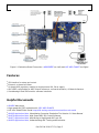
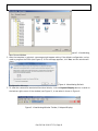
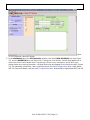
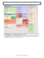
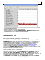
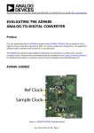
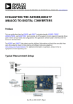
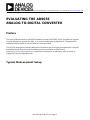
One Technology Way · P.O. Box 9106 · Norwood, MA 02062-9106 · Tel: 781.329.4700 · Fax: 781.461.3113 · www.analog.com
EVALUATING THE AD9656
ANALOG-TO-DIGITAL CONVERTER
Preface
This user guide describes the AD9656 evaluation board AD9656EBZ, which provides the support
circuitry required to operate the ADC in its various modes and configurations. The application
software used to interface with the device is also described.
The AD9656 data sheet provides additional information and should be consulted when using the
evaluation board. Documents and software tools are available at AD9656 and
www.analog.com/hsadcevalboard. For additional information or questions, send an email to
[email protected].
Typical Measurement Setup
Rev 20 Feb 2014 17:53 | Page 1
Figure 1. Evaluation Board Connection—AD9656EBZ (on Left) and HSC-ADC-EVALEZ (on Right)
Features
●
●
●
●
●
SPI interface for setup and control
External, on-board oscillator
On-board LDO regulator, needing a single external 6V, 2A dc supply
ADC VREF configurable for ADC-internal reference, on-board reference, off-board reference
VisualAnalog® and SPIController software interfaces
Helpful Documents
●
●
●
●
●
●
●
AD9656 data sheet
High speed ADC FIFO evaluation kit (HSC-ADC-EVALEZ)
HSC-ADC-EVALEZ Wiki Guide http://wiki.analog.com/resources/eval/hsc-adc-evald
AN-905 Application Note, VisualAnalog Converter Evaluation Tool Version 1.0 User Manual
AN-878 Application Note, High Speed ADC SPI Control Software
AN-877 Application Note, Interfacing to High Speed ADCs via SPI
AN-835 Application Note, Understanding ADC Testing and Evaluation
Rev 20 Feb 2014 17:53 | Page 2
Design and Integration Files
●
Schematics, layout files, bill of materials <Coming Soon>
Equipment Needed
●
●
●
●
●
●
●
●
Analog signal source(s) and antialiasing filter(s)
Sample clock source (if not using the on-board crystal oscillator)
Switching power supply (6.0V, 2.5A) for AD9656EBZ
Switching power supply (12V, 3,3A) for HSC-ADC-EVALEZ
PC running Windows®
USB 2.0 port
AD9656EBZ board
HSC-ADC-EVALEZ FPGA-based data capture kit
Getting Started
This section provides quick start procedures for using the AD9656EBZ board. Both the default and
optional ADC settings are described.
Configuring the Board
Before using the software for testing, configure the evaluation board as follows:
1. Connect the evaluation board to the data capture board, as shown in Figure 1.
2. On the ADC evaluation board, confirm that the jumpers are installed as shown in Figure 2.
3. The AD9656EBZ can be powered in one of three ways. The default is to have the AD9656EBZ
obtain its power from the HSC-ADC-EVALEZ through the FMC connector. For this configuration,
jumper pin 1 to pin 2 on both P101 and P103 on the AD9656EBZ. The other power configurations
will be described in the Power Supplies section below.
4. Connect the 12V, 3.3A switching power supply to the HSC-ADC-EVALEZ board.
5. Connect the HSC-ADC-EVALEZ board (P702) to the PC using a USB cable.
6. On the ADC evaluation board, use a clean signal generator with low phase noise to provide an
input signal to the desired channel(s). Use a shielded, RG-58, 50Ω coaxial cable (optimally 1 m or
shorter) to connect the signal generator. For best results, use a narrow-band, band-pass filter with
50Ω terminations and an appropriate center frequency. (Analog Devices, Inc. uses TTE, Allen
Avionics, and K&L band-pass filters.)
Rev 20 Feb 2014 17:53 | Page 3
Evaluation Board Hardware
The evaluation board provides the support circuitry required to operate the AD9656 in its various
modes and configurations. Figure 1 shows the typical bench characterization setup used to evaluate
AC performance. It is critical that the signal sources used for the analog input and clock have very low
phase noise (ideally ~100 fs rms jitter) to realize the optimum performance of the signal chain. Proper
filtering of the analog input signal to remove harmonics and lower the integrated or broadband noise
at the input is necessary to achieve the specified noise performance.
See AD9656 Design Support <Coming Soon> for schematics and layout diagrams. These diagrams
demonstrate the routing and grounding techniques that should be applied at the system level when
designing application boards using these converters.
Power Supplies
The AD9656EBZ can obtain its power from the HSC-ADC-EVALEZ through the FMC connector. P101
and P103 both need to have pin 1 tied to pin 2 for obtaining board power through the FMC connector
from the HSC-ADC-EVALEZ capture board. If P101 and P103 have pin 1 jumpered to pin 2, do not
connect the supplied 6V wall supply to the AD9656 evaluation board. When changing the
configuration of P101 and P103, please remove both jumpers and then place them in their desired
positions.
Alternatively, the AD9656EBZ can obtain its power from the wall-mountable 6V, 2A switching power
supply. For this mode, P101 and P103 both need to have pin 2 tied to pin 3. Connect the supply to a
100V ac to 240V ac, 47Hz to 63Hz wall outlet. The output from the supply is provided through a
2.1mm inner diameter jack that connects to the printed circuit board (PCB) at P102. The 6V supply is
fused and conditioned on the PCB before connecting to the low dropout linear regulators that supply
the proper bias to each of the various sections on the board.
Also, the evaluation board can be powered in a nondefault condition using external bench power
supplies. To do this, remove the E104, E105, E106, and E108 ferrite beads to disconnect the on-board
LDOs from the power planes. Note that in some board configurations some of these might already be
uninstalled. P104 and P105 headers can be installed to facilitate connection of external bench
supplies to the board. E110, E111, E112 and E113 need to be populated to connect P104 and P105 to
the board power domains. A 1.8V , 0.5A supply is needed for 1.8V_DUT_AVDD, 1.8V_DRVDD and
1.8V_DVDD. Although the voltage requirements are the same for these three, it is recommended that
separate supplies be used for each of these.
A 3.3V, 0.5A supply is needed for 3.3V_DIG, which is used to power additional on board circuitry.
Input Signals
The four channel inputs on the evaluation board are set up for a double balun-coupled analog input
Rev 20 Feb 2014 17:53 | Page 4
with a 50Ω impedance. When connecting the ADC clock and analog source, use clean signal
generators with low phase noise, such as the Rohde & Schwarz SMA, or an equivalent. Use a shielded,
RG-58, 50Ω coaxial cable (optimally 1 m or shorter) for connecting to the evaluation board. Enter the
desired frequency and amplitude (see the Specifications section in the data sheet). When connecting
the analog input source, use of a multipole, narrow-band band-pass filter with 50Ω terminations is
recommended. Analog Devices uses band-pass filters from TTE and K&L Microwave, Inc. Connect the
filters as close to the evaluation board as possible.
Clock
The default clock input circuit is derived from an on-board 125MHz crystal oscillator feeding through a
transformer-coupled circuit using a high bandwidth 1:1 impedance ratio transformer (T302) that adds
negligible jitter to the clock path. The external clock input (J302) is 50 Ω terminated and ac-coupled to
handle single-ended sinusoidal inputs. The transformer converts the single-ended input to a
differential signal that is clipped by CR301 before entering the ADC clock inputs. The AD9656 ADC is
equipped with an internal clock divider (programmable divide ratios of 1 through 8) to facilitate usage
with higher frequency clocks. When using the internal divider and a higher input clock frequency,
remove CR301 to preserve the slew rate of the clock signal.
The AD9656EBZ board is set up to be clocked through the transformer-coupled input network from
the 125MHz crystal oscillator, Y801. If an external clock source is desired, remove C302 (optionally)
and Jumper J304 to disable the oscillator from running and connect the external clock source to the
SMA connector, J302 (labeled CLOCK+).
If an external clock source is used instead of the onboard crystal oscillator, it should also be supplied
with a clean signal generator as previously specified for the analog input signals. Analog Devices
evaluation boards typically can accept ~2.8V p-p or 13 dBm sine wave input for the clock at the board
SMA clock connector.
Output Signals
The default setup uses the Analog Devices high speed converter evaluation platform (
HSC-ADC-EVALEZ) for data capture. The JESD204B outputs from the ADC are routed to P2 using 100Ω
differential traces. For more information on the data capture board and its optional settings, visit
www.analog.com/hsadcevalboard.
Jumper Settings
Set the jumper settings/link options on the evaluation board for the required operating modes before
powering on the board. The functions of the jumpers are described in Table 1. Figure 2 shows the
default jumper settings.
Rev 20 Feb 2014 17:53 | Page 5
Table 1. Jumper Settings
Jumper
P101,
P103
J304
J206
Description
These jumpers determine the power source for the AD9656EBZ.
Connect Pin 1 to Pin 2 on both P101 and P103 to power the ADC board from the
HSC-ADC-EVALEZ through the FMC connector.
Connect Pin 2 to Pin 3 on both P101 and P103 to power the ADC board from the wall
supply connected to P102.
Leave both P101 and P103 unjumpered if using headers P104 and P105.
This jumper enables the on-board crystal oscillator. Remove this jumper (and optimally
C302) if an external off-board clock source is used.
This jumper selects between internal VREF and external VREF.
To choose the ADC's internal reference, connect Pin 3 (DUT_SENSE) to Pin 5 (GND) as
shown in Figure 2. The default value of the internal reference is 1 V. SPI Register 0x18
Bits[7:6] can be used to program the internal reference voltage to values from 1 V to 1.4
V, in 0.1 V increments. Register control is accomplished with SPIController software,
which is discussed below in the Setting up the SPI Controller Software section.
To use the on-board AD822 buffered reference, connect Pin 2 (DUT_SENSE) to Pin 1
(AVDD), and connect Pin 4 (DUT_VREF) to Pin 6 (EXT_REF). Adjust external VREF to the
desired value (from 1.0 V to 1.4 V) using potentiometer R247.
To apply a reference voltage from an external off-board source, connect Pin 2
(DUT_SENSE) to Pin 1 (AVDD) and apply the reference voltage to Pin 4 (DUT_VREF). The
AD9656 reference voltage is specified to be from 1.0 V to 1.4 V.
Rev 20 Feb 2014 17:53 | Page 6
Figure 2. Default Jumper Connections for AD9656EBZ Board
How To Use The Software For Testing
Setting up the ADC Data Capture
The installers for VisualAnalog and SPIController are in the following locations:
ftp://ftp.analog.com/pub/HSSP_SW/VisualAnalog/VisualAnalog_Setup.exe
ftp://ftp.analog.com/pub/adispi/A2DComponents/Install/SPIController_Setup.exe
Run these installers on the PC that is connected to the evaluation setup before proceeding.
After configuring the board hardware, set up the ADC data capture using the following steps:
1. Start VisualAnalog on the connected PC. The appropriate part type should be listed in the status
bar of the VisualAnalog – New Canvas window. Select the template that corresponds to the type
of testing to be performed (see Figure 3). Average FFT is a good test to start with.
Rev 20 Feb 2014 17:53 | Page 7
Figure 3. VisualAnalog,
New Canvas Window
2. After the template is selected, a message might appear asking if the default configuration can be
used to program the FPGA (see Figure 4). If this message appears, click Yes, and the window will
close.
Figure 4. VisualAnalog Default
Configuration Message
3. To view the canvas and associated functional blocks, click the Expand Display button, located on
the bottom right corner of the window (see Figure 5), to see what is shown in Figure 6.
Figure 5. VisualAnalog Window Toolbar, Collapsed Display
Rev 20 Feb 2014 17:53 | Page 8
Figure 6. VisualAnalog, Main Window Expanded Display
4. To configure VisualAnalog to operate with the AD9656, push the Settings button on the
ADCDataCapture block, as shown in Figure 7.
Figure 7. VisualAnalog Window Toolbar, Collapsed Display
5. In the ADC Data Capture Settings Window, General Tab, select AD9656 to be the device, enter the
sample clock frequency (125 is the default value), as shown in Figure 8. The sample frequency
entered here is used for scaling of frequency values in test results and graphs. In the Output Data
field, the channels to be tested are selected, as well as the FFT capture depth (“Length”). Note that
the total of the capture depths for all selected channels cannot exceed 256k.
Rev 20 Feb 2014 17:53 | Page 9
Figure 8. VisualAnalog ADC Data Capture Settings Window, General Tab
6. In the ADC Data Capture Settings Window, Capture Board Tab, enter 60 in the Fill Delay field. Push
the Browse button to navigate to the FPGA program file for the AD9656. The default installation
location and filename will be similar to: C:\Program Files\Analog
Devices\VisualAnalog\Hardware\HADv6\AD9656_hadv6fmc.mcs
Push the program button.
Figure 9. VisualAnalog ADC Data Capture Settings Window, Capture Board Tab
7. In the ADC Data Capture Settings Window, Device Tab, check the Enable Data Capture Controls
Rev 20 Feb 2014 17:53 | Page 10
checkbox. The capture control fields will be enabled.
Select:
●
●
●
●
GTX RX Equalization: 6
Encode: 125MSPS (default configuration)
Number of lanes: 2 Lanes (At least 2 lanes are required for 125MSPS. The single lane bitrate at
125MSPS would exceed the driver and FPGA capabilities.)
Leave the other checkboxes unchecked.
Though the AD9656 supports a wide variety of converter/lane/sample rate configurations, the
software supports only the configurations in the software menu as an out-of-the-box functional kit. If
other sample rates or configurations are required, an additional external clock is likely needed.
Figure 10. VisualAnalog ADC Data Capture Settings Window, Device Tab
8. VisualAnalog is now setup to work with the AD9656EBZ in the default configuration. Other
VisualAnalog features and capture settings are documented in the AN-905 Application Note,
VisualAnalog Converter Evaluation Tool Version 1.0 User Manual.
Evaluation And Test
Setting up the SPI Controller Software
After the ADC data capture board setup is complete, set up the SPI controller software using the
following procedure:
1. Open the SPI controller software by going to the Start menu or by double-clicking the
Rev 20 Feb 2014 17:53 | Page 11
SPIController software desktop icon. If prompted for a configuration file, select .cfg file whose
name begins with AD9656. If not prompted, check the title bar of the window to determine which
configuration is loaded. If necessary, choose Cfg Open from the File menu and select the
appropriate file based on your part type. Note that the CHIP ID(1) box should be filled to indicate
whether the correct SPI controller configuration file is loaded (see Figure 11).
Figure
11. SPI Controller, CHIP ID(1) Box
2. Click the New DUT button in the SPIController window (see Figure 12)
Rev 20 Feb 2014 17:53 | Page 12
Figure
12. SPI Controller, New DUT Button
3. In the ADCBase0 tab of the SPIController window, find the CLOCK DIVIDE(B) box (see Figure
13), and the MODES(8) box (see Figure 14). If using the clock divider, use the drop-down box to
select the correct clock divide ratio, if necessary. If there is any interruption of the ADC clock
during power-up or during operation, a Digital Reset may be needed to re-initialize the ADC (Figure
14). For additional information, refer to the data sheet, the AN-878 Application Note, High Speed
ADC SPI Control Software, and the AN-877 Application Note, Interfacing to High Speed ADCs via SPI.
Rev 20 Feb 2014 17:53 | Page 13
Figure
13. SPI Controller, CLOCK DIVIDE(B) Box
Rev 20 Feb 2014 17:53 | Page 14
Figure
14. SPI Controller, Chip Power Mode - Digital Reset Selection
4. In the ADCBase1 tab of the SPIController window, set the number of lanes the AD9656 will be
configured to. Note that the number of lanes selected here must match the settings made in
VisualAnalog as shown in Step 7, Figure 10 above.
Rev 20 Feb 2014 17:53 | Page 15
Figure
15. SPI Controller, Quick Configure Box
5. Note that other settings can be changed on the ADCBase0 tab (see Figure 13) and the ADC A
through ADC D tabs (see Figure 16) to set up the part in the desired mode. The ADCBase0 tab
settings affect the entire part, whereas the settings on the ADC A through ADC D tabs each affect
the selected channel only. See the data sheet, the AN-878 Application Note, High Speed ADC SPI
Control Software, and the AN-877 Application Note, Interfacing to High Speed ADCs via SPI, for
additional information on the available settings.
Rev 20 Feb 2014 17:53 | Page 16
Figure
16. SPI Controller, Example ADC A Page
6. Invoke a Digital Reset as shown in Figure 14 before testing. After selecting Reset, select Chip run
to return to normal operation.
7. To begin testing, click the Run or Continuous Run button in the VisualAnalog toolbar (see
Figure 17).
Figure
17. Run/Continuous Run Buttons (Encircled in Red) in VisualAnalog Toolbar, Collapsed Display
Adjusting the Amplitude of the Input Signal
The next step is to adjust the amplitude of the input signal for each channel as follows:
1. Adjust the amplitude of the input signal so that the fundamental is at the desired level. Examine
the Fund Power reading in the left panel of the VisualAnalog Graph - AD9656 FFT window
(see Figure 18).
Rev 20 Feb 2014 17:53 | Page 17
Figure
18. Graph Window of VisualAnalog
2. Repeat this procedure for the other channels, if desired
3. Click the floppy-disk icon within the VisualAnalog Graph - AD9656 FFT window to save the
performance data as a .csv formatted file for plotting or analysis.
Troubleshooting Tips
Lack of SPI communication will cause difficulty in configuring the ADC.
●
●
●
●
Go to the Global tab of the SPIController window and push the Read button in the GENERIC
READ/WRITE window. This will read the contents of ADC register 0x00. If SPI communication is
working properly and the ADC is powered up, the value 0x18 hexadecimal will appear. If the
contents show 0x00, the ADC is not powered up or SPI communication is not working.
Check that there is correct power to the AD9656EBZ board, and to the HSC-ADC-EVALEZ.
Check that the USB cable is properly connected from the PC to the HSC-ADC-EVALEZ.
The LED on the VisualAnalog ADCDataCapture block should be green. If it is red, push the USB
button on the same block to refresh the connection.
If the FFT plot appears abnormal, do the following:
●
●
●
If you see an abnormal noise floor, go to the ADCBase0 tab of the SPIController window and
toggle the Chip Power Mode in MODES(8) from Chip Run to Reset and back (Figure 14).
If you see a normal noise floor when you disconnect the signal generator from the analog input, be
sure that you are not overdriving the ADC. Reduce the input level, if necessary.
In VisualAnalog, click the Settings icon in the Input Formatter block. Check that Number
Rev 20 Feb 2014 17:53 | Page 18
Format is set to the correct encoding (twos complement by default). Check that the Number
Format in the VisualAnalog Input Formatter matches the data format selected in the
SPIController ADCBase0 OUTPUT MODE(14) window. Repeat for the other channels.
If the FFT appears normal but the performance is poor, check the following:
●
●
●
●
Make sure that an appropriate filter is used on the analog input.
Make sure that the signal generators for the clock and the analog input are clean (low phase noise).
Change the analog input frequency slightly if noncoherent sampling is being used.
Make sure that the SPI configuration file matches the product being evaluated.
If the FFT window remains blank after Run in VisualAnalog (see Figure 17) is clicked, do the following:
●
●
●
●
Make sure that the evaluation board is securely connected to the HSC-ADC-EVALEZ board.
Make sure that the correct FPGA program was installed by clicking the Settings icon in the ADC
Data Capture block in VisualAnalog. Then select the FPGA tab and verify that the proper FPGA
.mcs file (one containing “AD9656” in the filename) is selected for the part.
Make sure that the FPGA has been programmed by verifying that the CONFIG_DONE LED is
illuminated on the HSC-ADC-EVALEZ board. If the CONFIG_DONE LED is not illuminated, click the
Settings icon in the ADC Data Capture block in VisualAnalog. Then select the FPGA tab and
verify that the proper FPGA .mcs file (one containing “AD9656” in the filename) is selected for the
part. Then push the Program button. The LED should light up.
On the AD9656EBZ there is an LED next to a reset button (S501). If this LED is not lit, push the reset
button and try running again.
© Analog Devices, Inc. All rights reserved. Trademarks and
registered trademarks are the property of their respective owners.
Rev 20 Feb 2014 17:53 | Page 19
www.analog.com