1
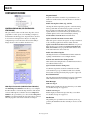
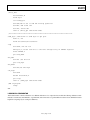
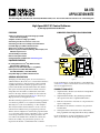
AN-878 APPLICATION NOTE One Technology Way • P.O. Box 9106 • Norwood, MA 02062-9106, U.S.A. • Tel: 781.329.4700 • Fax: 781.461.3113 • www.analog.com High Speed ADC SPI Control Software by the High Speed Converter Division FEATURES SIMPLIFIED FUNCTIONAL BLOCK DIAGRAM Simple user interface for all standard high speed ADC devices with SPI capability Simplifies evaluation of high speed ADCs Automatic generation of end use C source code Automatic generation of assembly code for PIC12F629 Used with high speed ADC evaluation boards Allows access to all user-controlled features Works in conjunction with VisualAnalog, ADC Analyzer, and ADC data capture board Standard USB port interface Built-in web update feature Configuration files available from www.analog.com STANDARD USB 2.0 REG ADC PS +3.0V REG LOGIC FILTERED ANALOG INPUT PC running Windows 98 (2nd Ed), Windows 2000, Windows ME, or Windows XP USB 2.0 port recommended (USB 1.1 compatible) Data capture board (HSC-ADC-EVALB-SC, HSC-ADC-EVALB-DC, or HSC-ADC-EVALC) Compatible high speed ADC evaluation board CHB FIFO, 32K, 133MHz n TIMING CIRCUIT USB CTLR CHA FIFO, 32K, 133MHz n CLOCK CIRCUIT SPI SPI CLOCK INPUT GENERAL DESCRIPTION 120-PIN CONNECTOR The high speed ADC SPI program, version 2 and version 3, (SPIController.exe) allows the user to control advanced features on high speed, analog-to-digital converters (ADC) with SPI capability. This advanced controller program is used in con junction with the HSC-ADC-EVALB or HSC-ADC-EVALC data capture boards and specific device evaluation boards to manipulate and control SPI-accessible features. More infor mation on the range of features available can be found in the specific device data sheets and in the AN-877, Interfacing to High Speed ADCs via SPI application note. The SPI Controller program can run as a standalone application on a Windows® platform, or in conjunction with any available data analysis tool, such as VisualAnalog™ or ADC Analyzer™. The software includes advanced features to ensure a smooth transition from evaluation into prototyping and production. When a desired configuration is attained, the program includes a C-code generator that provides compatible C source code that can be incorporated into customer-developed software. For users without an available microcontroller, the software also includes an assembly code generator that produces code targeted for the ultralow cost PIC12F629 microcontroller. 05949-001 PS EQUIPMENT NEEDED HSC-ADC-EVALB-SC OR HSC-ADC-EVALB-DC SINGLE OR DUAL HIGH-SPEED ADC EVALUATION BOARD Figure 1. For more information on using this device to control SPI devices, see the AN-812, Microcontroller-Based Serial Port Interface (SPI) Boot Circuit application note. PRODUCT HIGHLIGHTS 1. Graphic Interface. Intuitive user interface for manipulation of all on-chip registers. 2. Simple Hardware Interface. Easy interfacing with ADC data capture boards and a compatible USB interface. 3. Built-In Code Generator. Automatic C-code generation for register configuration. 4. PIC12F629 Code Generator. Automatic code generation for PIC12F629. 5. Web Update Feature. This feature ensures that both the latest program files and configuration files are always available. For more information on using and interfacing to the SPI device, see the AN-877 and AN-812 application notes. Rev. A | Page 1 of 20 AN-878 TABLE OF CONTENTS Features .............................................................................................. 1 Perform New DUT function during NewCal ...................8 Equipment Needed........................................................................... 1 Ignore Transfer function during write ...............................8 General Description ......................................................................... 1 Read Channel Index .............................................................8 Simplified Functional Block Diagram ........................................... 1 Error Messages ..........................................................................8 Product Highlights ........................................................................... 1 USB error msg en..................................................................8 Revision History ............................................................................... 2 Transfer error msg en ...........................................................8 Quick Start......................................................................................... 3 Parallel Port................................................................................8 Installing the Program ................................................................. 3 Script Dialog ..................................................................................9 Running the Program .................................................................. 3 Typical C Source Code Generated..........................................9 Powering Down ............................................................................ 3 Launch Page ReadBack.............................................................. 13 Getting Started .................................................................................. 4 Launch ASM Code Generator .................................................. 13 Device Check ................................................................................ 5 Typical PIC12F629 ASM Code ........................................ 14 SPI Control Panel ............................................................................. 6 Launch Cal Comparator............................................................ 17 File Menu ........................................................................................... 7 Help Menu....................................................................................... 18 Cfg Open ....................................................................................... 7 Current Files................................................................................ 18 Cfg Save As .................................................................................... 7 Device Cfg Filename.............................................................. 18 Cal Open........................................................................................ 7 Device Cal Filename .............................................................. 18 Cal Save As .................................................................................... 7 Script Filename....................................................................... 18 Download Files from FTP Site.................................................... 7 Script Log Filename ............................................................... 18 Exit.................................................................................................. 7 ASM Filename ........................................................................ 18 Configuration Menu ........................................................................ 8 Rev History ................................................................................. 18 Controller Dialog (SPI Controller Cfg Dialog) ....................... 8 USB Info ...................................................................................... 18 FIFO Chip Select Number (USB FIFO Channel Number) 8 Help Topics.................................................................................. 18 Program Control ...................................................................... 8 SPI Controller User Manual...................................................... 18 Enable Auto Update of DLL, Cfg., Cal files ...................... 8 ADI SPI Protocol User Manual ................................................ 18 Update Controller From DUT on New DUT................... 8 Tool Bar............................................................................................ 19 Enable Auto Channel Update ............................................. 8 REVISION HISTORY 4/07—Initial Version to Rev. A Updated Format..................................................................Universal Changed Name of High Speed ADC Controller Quick Start Set Up (SPI) Section to Quick Start Section ........................ 3 Replaced Figure 2 ............................................................................. 4 Changes to Running the Program Section.................................... 3 Replaced the Device Check Section............................................... 5 Replaced Figure 6 ............................................................................. 6 Replaced Figure 7 and Figure 8 ...................................................... 7 Replaced Figure 9 ............................................................................. 8 3/06—Revision 0: Initial Version Rev. A | Page 2 of 20 AN-878 QUICK START The SPI controller program (SPIController.exe) provides access to high speed converters that are SPI enabled. Running this program opens a window that provides complete control of available functions of the converters. For available functions and full programming details, see the AN-877, Interfacing to High Speed ADCs via SPI application note. Because supported features vary by device, refer to the specific device data sheets. Although this application note explains the features of the SPI controller program, it does not fully document SPI. INSTALLING THE PROGRAM Although this program runs without hardware attached, it does require the HSC-ADC-EVALB or HSC-ADC-EVALC boards to be fully functional. These data capture boards include an SPI Controller and are required to interface to SPI-enabled high speed converter evaluation boards. Consult the specific device data sheets to determine compatibility. Install the SPI Controller by one of the following methods: • The SPI Controller program can be installed as part of ADC Analyzer, version 4.9.0 and later. This program, provided on CD with the data capture board, can also be downloaded from www.analog.com/fifo. Insert the disk or run the downloaded file to install both applications. • A separate SPI Controller installation program is available from www.analog.com/fifo. This installation does not include ADC Analyzer. Download the zip file and then extract it to a temporary directory. Run the setup.exe application and follow the instructions that display. • A separate installer (the most current version available) can be found at ftp.analog.com/pub/adispi/A2DComponents/Install 2. Turn on the HSC-ADC-EVALB-xx or HSC-ADC-EVALC board and the ADC evaluation board (if connected). 3. Connect the USB cable between the computer and the HSC-ADC-EVALB-xx or HSC-ADC-EVALC board. Windows then recognizes the evaluation board and registers the drivers. After driver registration is complete, the software is ready to use once Windows indicates that the new hardware is ready to use. • The software checks to ensure that hardware is present and that a SPI-compatible device is connected to the evaluation board. If the hardware is not present and/or the correct device is not connected, a series of warning message may be displayed. Although warnings are provided, the program continues to run. The first time the program is run, it prompts for a configuration file after several warnings are displayed. The file browser displays available configurations. If available configurations are not displayed, set the browser to the location on the hard disk where the configuration files are stored. This is usually the installation directory. Additional configuration files can be downloaded from the product page at www.analog.com or are shipped with your evaluation board. For the most up-to-date configuration files, web updates are also available. See the Download Files from FTP Site section of this application note. If you still cannot locate the desired configuration file, email Analog Devices at [email protected] and request the latest SPI configuration file for the device. If the program has run before, the last configuration selected is used. To change the configuration, open the File menu and select Cfg Open. Select the file corresponding to the selected device. At power-up, the device should be running with default values in the registers. These are typically a nominal state to ensure that the device is functional. Because each converter has a different set of supported features, the device data sheet should be consulted. All devices support at least power-down features in the mode setting. Follow these steps to place the device in power-down mode. 1. Windows must register the drivers. To accomplish this, set up the HSC-ADC-EVALB-xx or HSC-ADC-EVALC data capture board. Although it is not necessary to have an ADC evaluation board connected at this point, if one is available, this is a good time to install it. Run the program from one of two available methods: Double click the SPIController desktop shortcut. POWERING DOWN After installing the software, follow these steps: RUNNING THE PROGRAM • 1. Make sure that the Asynchronous Transfer Enabled option is selected. This ensures that as each control is changed, it is immediately sent to the device through the SPI. 2. Select the ADCBase, ADCBase0, or ADCGlobal 0 tab to display the appropriate page and locate the mode register (0x08h). Then, under the Int Pwr Dn window, click the Full Pwr Dn radio button. This shuts the device down by writing the corresponding value to the mode register. If a current meter is available, this can be observed on the readout. 3. Click Chip Run and the device starts again. Other features of the device can be explored by clicking the appropriate button, check box, or text box. Commands are sent immediately to the device as long as Asynchronous Transfer Enabled is selected. If not enabled, then commands are manually issued by clicking the Transfer button. For a description of the Transfer button, see Table 2. From the Start menu, under Analog Devices, select the SPIController. Rev. A | Page 3 of 20 AN-878 GETTING STARTED The Quick Start section of this application note briefly described how to install and run the SPIContoller software and how to power down the device. The remainder of this application note provides an expanded explanation on how to use the SPI Controller software. When the SPI Controller program is launched for the first time, it begins searching for the required hardware and configuration files. Warning messages appear if these files cannot be located. 2. Select the configuration file associated with the device evaluation board currently connected to the bench equipment and then click Open. Because all ADCs follow the same SPI protocol and memory map, selecting an incorrect configuration does not damage the device and may actually provide some degree of control. Use the correct configuration, however, to ensure that all features available for a given device are accessible. 05949-002 1. Click OK in response to each of the warning messages until the program prompts for a configuration file. The configuration file determines how the user interface is configured and is selected depending upon which device you are using. Figure 2. File Browsing Rev. A | Page 4 of 20 AN-878 DEVICE CHECK Once the appropriate configuration file is selected, the evaluation board status is tested. The device installed on the evaluation board is also checked. If errors are reported, the software continues to run after clicking OK in response to the warning messages. If the cable is correctly connected, the user may click Ignore (see Figure 4 to conclude the start-up sequence, otherwise the start-up sequence repeats once to allow the user to make cable connections. If the error is due to an incorrect chip select assignment, the chip select can be changed after the software finishes the start-up sequence 05949-003 The software first checks for an available HSC-ADC-EVALB-xx or HSC-ADC-EVALC data capture board. If this board is not connected, an error message (see Figure 3) displays and a read test failure occurs. Figure 3. Typical USB Error Message When a data capture board is located, the software checks to see which ADC is connected to the board. If the correct configuration file is not selected, or if an incorrect board is connected, an error message displays with the requested device name listed. 05949-004 Click OK to indicate that the program should continue without the hardware. 05949-016 Figure 4. Chip ID Error Message Figure 5. Chip ID Error Message Rev. A | Page 5 of 20 AN-878 SPI CONTROL PANEL The SPI control panel provides a graphical way of interacting with the device connected to the SPI interface. Because each device can have a different set of registers, the user interface varies from part to part. For details on each feature, refer to the AN-877, Interfacing to High Speed ADCs via SPI application note. Consult the device data sheet to determine which features are available for each device. This application note provides an overview of the software capabilities and does not attempt to address the implications of each available device function. If the device has multiple ADCs, features local to each ADC channel are shown on the ADC A through ADC Z tabs. For a single ADC, only the ADCBase 0 tab is available. Not all converters support all features and, therefore, the specific device data sheet should be consulted to determine what individual features are available, and how the part will respond to the values programmed. Auxiliary ADC functions are found on additional pages, accessible by selecting tabs, which are labeled accordingly. If more than one page is required, multiple pages are included. These are device-specific functions and documentation can be found in the specific device data sheet. Some converters have additional pages not documented here. Again, consult the specific device data sheet for information regarding those features. In general, functionality of those features is consistent with features documented here. 05949-005 Each tab on the SPI Controller user interface contains a different set of controls. The Global tab contains features that apply globally to the SPI device and is limited to the configuration of the physical interface for features, such as SPI interface, LSB first, or chip soft reset. The settings of all controls indicate the state programmed into the chip. Common ADC features are found on the ADCBase 0 page accessible by selecting the ADCBase 0 tab. Figure 6. Typical User Interface—Appearance May Vary by Device Rev. A | Page 6 of 20 AN-878 FILE MENU The File menu allows for loading and saving of various configuration files as shown in Figure 7. CAL OPEN Cal Open allows the user to retrieve setup information. The option to retrieve previously saved registers settings can expedite setting a device in a desired state. CAL SAVE AS 05949-006 When the registers of a device are in a desirable state, they can be saved in a file for future use. This is accomplished by selecting Cal Save As and supplying a new file name when prompted. DOWNLOAD FILES FROM FTP SITE Figure 7. File Menu CFG OPEN The SPI Controller works with most AD92xx, AD94xx, and AD66xx data converters that support an SPI port (see the device data sheet for details). To configure the controller for the applicable device, select Cfg Open and choose the configuration file for that device. Configuration files are supplied with this software or the evaluation boards, and are also available at www.analog.com. Web updates are also available as documented in the Download Files from FTP Site section of this application note. If required configuration files cannot be located by any of these means, they can be request by contacting [email protected]. CFG SAVE AS If a configuration file has changed, it can be saved under a new name for future use by selecting this option. The program prompts for a new filename. This option allows new configurations to be directly down loaded from the Analog Devices, Inc. public FTP site. This is the quickest and easiest way to ensure that the configuration files and the executable files in use are completely up to date. Similarly, if you have an evaluation board without a configuration file, this is the first place you should look. When you click this option, you are given notice that data will be copied from the Analog Devices public FTP site with the option to cancel if desired. If you select Yes, the program saves your current configuration, exits the program, executes the update program and then reruns the program, taking care to reload your last configuration. Alternatively, configurations may be manually downloaded from the product website at www.analog.com or you may request them by contacting [email protected] and asking for the latest SPI configuration file for the device. EXIT To close down the SPI Controller program, click Exit. Rev. A | Page 7 of 20 AN-878 CONFIGURATION MENU Program Control 05949-007 Program Control allows a number of optional features to be enabled. To enable a feature, select the check box to the left of the feature. Enable Auto Update of DLL, Cfg., Cal files Figure 8. Config Menu CONTROLLER DIALOG (SPI CONTROLLER CFG DIALOG) This option allows selection of the device chip select, various program flow control options, error handling (see Figure 9), and alternative interfacing options. In general, these selections do not need to be changed because they are set during the configuration process for the device. However, the ability to change selections can be useful for advanced users. Selecting this feature signals the program to search the Analog Devices public FTP site each time the program is run for the latest program and configuration files. Selecting this option requires Internet access and should only be checked if access is available. Updates can be retrieved manually by selecting Download Files from FTP Site from the File menu. Update Controller From DUT on New DUT When this option is selected, the registers on-chip is transferred to the controller graphical user interface (GUI) when the Update Controller From DUT on New DUT button is pressed. If this check box is not checked, the Update Controller From DUT on New DUT button programs the DUT with the values in the GUI. DUT is the device under test. Enable Auto Channel Update Checking this check box with multichannel ADCs enables the updating of similar features across multiple channels. Perform New DUT function during NewCal When checked, the GUI performs a new DUT function when a new calibration file is loaded. Ignore Transfer function during write Not all ADCs require that a transfer command be sent after each command or group of commands. If this box is checked, the automatic transfer generated by this program is suppressed. Read Channel Index 05949-008 The value in the Read Channel Index drop-down box determines which ADC channel is accessed during a readback cycle. Error Messages USB error msg en Figure 9. SPI Controller Cfg Dialog Box FIFO Chip Select Number (USB FIFO Channel Number) The FIFO Chip Select Number menu allows you to configure the SPI Controller to activate the chip select line of the desired converter. Although most evaluation boards use Chip Select Number 1, this option allows you to select another Chip Select Number as needed. By default, the appropriate value is selected when the program is run and do not need to be changed. Enables display of USB error messages when they occur. When not checked, messages are suppressed. Transfer error msg en Enables display of transfer messages when they occur. When not checked, messages are suppressed. Parallel Port The parallel port is provided for devices that may not be sup ported by the USB SPI Controller. Currently, no devices use this interface. Rev. A | Page 8 of 20 AN-878 SCRIPT DIALOG This option allows the creation of log, pseudocode (C code), and assembly (PIC12F629) files to be enabled (see Figure 10). If the software is included as part of an end application, the user must supply the hardware-specific read and write utilities. This feature helps users understand how to program the device. The example code that follows shows a typical programming sequence as written to a script file. These files are annotated and they describe the sequence of setting the file. 05949-009 The log file is a record of the commands sent to the SPI port during the period where this feature is enabled, which functions much like a record macro session. Enable or disable this option by checking or not checking the box, respectively. For historical and documentation purposes, this feature is useful in looking back at what commands were sent. This file is appended to and continues to be appended to until Clear is clicked. The script file contains the C code file, which represents the sequence of data passed to the SPI port of the device. This file can be used as a programming reference or can be included in the end application source code. The format follows standard C/C++ syntax. Figure 10. SPI Files Dialog BoxTypical C Source Code Generated //The following code exemplifies usage of the generated script or log file. // declarations for wrapper functions ********** // void SPIwrite(int address, int value); // int SPIread(int address); // definitions of wrapper functions ************ // void SPIwrite(int address, int value) // { // place compiler specific 'write' function here, i.e. // void write(int address, int value); // } // int SPIread(int address) Rev. A | Page 9 of 20 AN-878 // { // place compiler specific 'read' function here, i.e. // int read(int address); // } // sample pgm ************************** // void main() // { // int x; // SPIwrite(22,4); // x = SPIread(22); // } // *********************************** SPIwrite(0000,18); //chip_port_config 2/7/2006 10:40:11 PM SPIwrite(0005,0F); //device_index_2 2/7/2006 10:40:11 PM SPIwrite(00FF,00); //device_update 2/7/2006 10:40:11 PM //ADC A SPIwrite(0008,00); //modes 2/7/2006 10:40:11 PM SPIwrite(0009,01); //clock 2/7/2006 10:40:11 PM SPIwrite(000D,00); //test_io 2/7/2006 10:40:11 PM SPIwrite(000F,60); //adc_input 2/7/2006 10:40:11 PM SPIwrite(0014,00); //output_mode 2/7/2006 10:40:11 PM SPIwrite(0015,00); //output_adjust 2/7/2006 10:40:11 PM SPIwrite(0016,03); //output_phase 2/7/2006 10:40:11 PM SPIwrite(0018,03); //vref 2/7/2006 10:40:11 PM SPIwrite(0019,00); //user_patt1_lsb 2/7/2006 10:40:11 PM SPIwrite(001A,00); //user_patt1_msb 2/7/2006 10:40:11 PM SPIwrite(001B,00); //user_patt2_lsb 2/7/2006 10:40:11 PM SPIwrite(001C,00); //user_patt2_msb 2/7/2006 10:40:11 PM SPIwrite(0021,00); //serial_control 2/7/2006 10:40:11 PM SPIwrite(0022,00); //serial_ch_stat 2/7/2006 10:40:11 PM //ADC B SPIwrite(0008,00); //modes 2/7/2006 10:40:11 PM SPIwrite(0009,01); //clock 2/7/2006 10:40:11 PM SPIwrite(000D,00); //test_io 2/7/2006 10:40:11 PM SPIwrite(000F,60); //adc_input 2/7/2006 10:40:11 PM SPIwrite(0014,00); //output_mode 2/7/2006 10:40:11 PM Rev. A | Page 10 of 20 AN-878 SPIwrite(0015,00); //output_adjust 2/7/2006 10:40:11 PM SPIwrite(0016,03); //output_phase 2/7/2006 10:40:11 PM SPIwrite(0018,03); //vref 2/7/2006 10:40:11 PM SPIwrite(0019,00); //user_patt1_lsb 2/7/2006 10:40:11 PM SPIwrite(001A,00); //user_patt1_msb 2/7/2006 10:40:11 PM SPIwrite(001B,00); //user_patt2_lsb 2/7/2006 10:40:11 PM SPIwrite(001C,00); //user_patt2_msb 2/7/2006 10:40:11 PM SPIwrite(0021,00); //serial_control 2/7/2006 10:40:11 PM SPIwrite(0022,00); //serial_ch_stat 2/7/2006 10:40:11 PM //ADC C SPIwrite(0008,00); //modes 2/7/2006 10:40:11 PM SPIwrite(0009,01); //clock 2/7/2006 10:40:11 PM SPIwrite(000D,00); //test_io 2/7/2006 10:40:11 PM SPIwrite(000F,60); //adc_input 2/7/2006 10:40:11 PM SPIwrite(0014,00); //output_mode 2/7/2006 10:40:11 PM SPIwrite(0015,00); //output_adjust 2/7/2006 10:40:11 PM SPIwrite(0016,03); //output_phase 2/7/2006 10:40:11 PM SPIwrite(0018,03); //vref 2/7/2006 10:40:11 PM SPIwrite(0019,00); //user_patt1_lsb 2/7/2006 10:40:11 PM SPIwrite(001A,00); //user_patt1_msb 2/7/2006 10:40:11 PM SPIwrite(001B,00); //user_patt2_lsb 2/7/2006 10:40:11 PM SPIwrite(001C,00); //user_patt2_msb 2/7/2006 10:40:11 PM SPIwrite(0021,00); //serial_control 2/7/2006 10:40:11 PM SPIwrite(0022,00); //serial_ch_stat 2/7/2006 10:40:11 PM //ADC D SPIwrite(0008,00); //modes 2/7/2006 10:40:11 PM SPIwrite(0009,01); //clock 2/7/2006 10:40:11 PM SPIwrite(000D,00); //test_io 2/7/2006 10:40:11 PM SPIwrite(000F,60); //adc_input 2/7/2006 10:40:11 PM SPIwrite(0014,00); //output_mode 2/7/2006 10:40:11 PM SPIwrite(0015,00); //output_adjust 2/7/2006 10:40:11 PM SPIwrite(0016,03); //output_phase 2/7/2006 10:40:11 PM SPIwrite(0018,03); //vref 2/7/2006 10:40:11 PM SPIwrite(0019,00); //user_patt1_lsb 2/7/2006 10:40:11 PM SPIwrite(001A,00); //user_patt1_msb 2/7/2006 10:40:11 PM SPIwrite(001B,00); //user_patt2_lsb 2/7/2006 10:40:11 PM SPIwrite(001C,00); //user_patt2_msb 2/7/2006 10:40:11 PM SPIwrite(0021,00); //serial_control 2/7/2006 10:40:11 PM Rev. A | Page 11 of 20 AN-878 SPIwrite(0022,00); //serial_ch_stat 2/7/2006 10:40:11 PM //AUX 0 SPIwrite(0022,00); //serial_ch_stat 2/7/2006 10:40:11 PM //AUX 1 SPIwrite(0022,00); //serial_ch_stat 2/7/2006 10:40:11 PM SPIwrite(00FF,01); // write transfer bit 0 = SPIread(00FF); // read transfer bit Rev. A | Page 12 of 20 AN-878 ASMFilename sets the file name used for the creation of the PIC12F629 assembly code. See the Launch ASM Code Generator section for details on how to generate these files. Additional information can be found in the AN-812, Microcontroller-Based Serial Port Interface (SPI®) Boot Circuit application note. LAUNCH ASM CODE GENERATOR FTP Site Address is the address used by the update software to load the most current executables and configurations. Although this typically should not be changed, this option allows you to do so when necessary, for example, if the site is moved in the future. The ASM Code Generator is used with the Microchip® PIC12F629 on the evaluation board (see Figure 12). This circuit can be copied and placed on end-user boards for a very low cost SPI controller. The code generator is an easy method of collecting configuration data. The data is then assembled with the PIC compiler and written to the device to initialize the desired conditions. Additional details can be found in the AN-812 application note. LAUNCH PAGE READBACK Three buttons, shown in Table 1, on the ASM Code Generator dialog box aid in the collection of the configuration data. The Page ReadBack feature allows the on-chip memory of the connected device to be read (see Figure 11). Button Table 1. ASM Code Generator Buttons Clicking the Read button initiates the readback and comparison process. The display opens in a separate window allowing the main controller window to continue to operate independent of the ReadBack page. This makes it easy to change the values and then to verify that the device properly received the data. The ReadBack page indicates which tab the register is on, a description of the register, the address, and the written and read values. For clarity, a pass/fail flag is written. This feature is useful for debugging a device. Description The Record button begins recording key strokes. While recording, as controls change, their values are recorded in the ASM Code Generator until recording stops. When this button is pressed again, it changes into the Stop Record button. The Erase button erases recorded commands. Use this button to correct commands or to erase commands so that new commands can be entered. The Write button writes the completed macro to a file. The file used is specified in the SPI Files Dialog (see Figure 10). This feature, in conjunction with the main interface, allows the complete user memory map to be written to and then explored. 05949-014 The ASM Code Generator dialog box (see Figure 12), shows the sequence of commands that enables all four ADCs in Index Register 5, disables the duty cycle stabilizer, and starts the chip. 05949-015 Figure 11. Page ReadBack Dialog Box Figure 12. ASM Code Generator Dialog Box Rev. A | Page 13 of 20 AN-878 Typical PIC12F629 ASM Code ; This is the SPI_control ASM file used to configure the PIC12F629 for the SPI boot circuit ; Code for the PIC12F629 SPI boot circuit #define _version '0.10' ;Update History: ;Application Description/Comments ;Author: Steve Ranta and Alfredo Barriga ;Hardware Notes list p=12F629 ;Device Specification #include <p12F629.inc> ;Include files/registers ;Variable/registers declarations ;Macros (Configuration parameters> Internal RC oscillator and Watchdog timer disabled __CONFIG _CP_OFF & _CPD_OFF & _BODEN_OFF & _WDT_OFF & _MCLRE_ON & _WDT_OFF & _PWRTE_ON & _INTRC_OSC_NOCLKOUT ;Parameters for the configuration register ;Define Port Variables and pin assignent #define SCLK GPIO,0 ;defines clock pin in GPIO,0 (SPI clock) #define CSB GPIO,2 ;defines CSB pin in GPIO,2 (Chip enable signal) #define SDO GPIO,1 ;defines SDO pin in GPIO,1 (SPI data in) #define LED GPIO,4 ;defines LED pin in GPIO,4 (LED indicator for busy state) ;*********************Variable Definitions***************** ;Variables are stored in these general purpose registers upperaddress EQU 0x20 loweraddress EQU 0x21 SPIdata EQU 0x22 bitcounter EQU 0x23 byte EQU 0x24 ORG 0x000 ;calibrate internal oscillator with factory settings ;Initialize all internal peripherals and ports for SPI functions bcf STATUS,RP0 ;Select Bank 0 clrf GPIO ;Initializes GPIO register movlw 07h ;Setting up value for comperator module <CM2,CM1,CM0>=<111> movwf CMCON ;comparator module off(digital out) bsf STATUS,RP0 ;select Bank 1 movlw b'00001000' ;literal to set all port pins as output except for GPIO.3 (reset) movwf TRISIO ;direction bits moved to TRISIO bcf STATUS,RP0 ;clear register bank select Rev. A | Page 14 of 20 AN-878 ;******************************************************* ;Initializes outputs INIT bsf CSB; sets CSB bcf SCLK;clears SCLK bcf SDO; clears SDO bcf LED;clears LED (LED is off) clrf bitcounter ;clear bitcounter register clrf byte; clear byte register ;Since we are performing writing operations, and the SPI mode is MSB first, 16-bit addressing ;the first register value, which is the instruction register will always be h'00' ;----------------------------------------------------------------------------------------- ---------------movlw h'00' movwf upperaddress ;****************************************************** ;****************************************************** ;This section of the program is generated by SPIController, and will contain the register ;address and data values the user has specified. movlw h'0005' movwf loweraddress movlw h'01' movwf SPIdata call write_SPI movlw h'0005' movwf loweraddress movlw h'03' movwf SPIdata call write_SPI movlw h'0005' movwf loweraddress movlw h'07' movwf SPIdata call write_SPI movlw h'0005' movwf loweraddress movlw h'0F' movwf SPIdata Rev. A | Page 15 of 20 AN-878 call write_SPI movlw h'0009' movwf loweraddress movlw h'00' movwf SPIdata call write_SPI movlw h'0008' movwf loweraddress movlw h'00' movwf SPIdata call write_SPI ;************************************************************** ;************************************************************** ;This is the last part of the program. Here, an UPDATE DEVICE command is executed to transfer ;data from the buffers to the SPI port. ;Sleep command is executed after all registers have been updated, and the device goes to sleep ;until reset or power on. ;Update register: FFh, value:h'01' movlw h'FF' movwf loweraddress movlw h'01' movwf SPIdata call write_SPI sleep ;************************************************************************** write_SPI ;routine that writes data to the SPI port bsf LED ;LED turns ON indicating writing process has started bcf CSB; CSB pin goes low to start a writing command ;Write_upperaddress movf upperaddress,W ;transfer upperaddress to W register movwf byte call send_byte ;call send_byte subroutine ;Write_loweraddress movf loweraddress,W movwf byte call send_byte; write lower address into SPI Rev. A | Page 16 of 20 AN-878 ;write_data movf SPIdata,W movwf byte call send_byte bsf CSB;CSB is set to end SPI writing operation bcf LED; Led turns off bcf SDO; clears sdo retlw 0 ;Write_spi subroutine ends. ;**************************************************************************** send_byte ;subroutine to send byte to spi port movlw 8; w=8 movwf bitcounter;bitcounter=8 loop bcf SCLK; clk set low RLF byte,F ;rotate each bit to the left through carry in STATUS register btfsc STATUS,C goto SDO_HIGH SDO_LOW bcf SDO ;Set SDO low goto clk_high SDO_HIGH bsf SDO;Set SDO high clk_high bsf SCLK decfsz bitcounter,F goto loop retlw 0 ;send_byte subroutine ends ;End of program sleep END LAUNCH CAL COMPARATOR This feature launches a window that allows two different calibrations to be compared. These include the following calibrations: DUT Default to Current State, DUT Default to a Specified File, and Current State to Specified File. The advanced user will find this feature helpful for comparing any two settings for differences. Rev. A | Page 17 of 20 AN-878 HELP MENU Device Cal Filename 05949-010 This file contains the default values for each on-chip register. The initial file provided with the software contains default chip values. New Cal files can be created that allow you to set different defaults. Script Filename Figure 13. Help Menu The C code generator writes to this file. Because it is generated with the same data that is sent to the USB SPI Controller, it is representative of the same information used to program the device from the evaluation board. This code includes embedded documentation to enhance readability. Although the code is fully usable, it is not optimized. Various programming techniques exist to improve the optimization of the code for both speed and size. This code is provided as a starting point to ensure that you have reference code that is helpful for device configuration. CURRENT FILES The Current Files menu provides a summary of important file names used in various parts of the program (see Figure 14). These file names can be changed using the Config menu (see the Script Dialog section). Changes can be made to Cfg and Cal files, as well as scripting and dialog files. 05949-011 Script Log Filename Figure 14. SPI Files Dialog Box Device Cfg Filename This file, used to configure the program for the device, contains the registers and bit information for the device. Register and bit information is available with this software package, from www.analog.com, or by using the FTP download feature (see the Download Files from FTP Site section). If the installation CD does not provide a configuration for the converter, contact [email protected]. The instructions are logged to this file. When this feature is enabled, all instructions that pass to the device are also written to this file, creating a log of all commands written to the device. This is an appended file containing the program history of the device (until the file is cleared). It is useful when debugging to see what commands were issued to the device that may have or may not have worked. ASM Filename When the PIC12F629 assembly code generation option is selected, this file is written to. See the AN-812 application note for more details on this file. REV HISTORY This option provides details of the history of this software. USB INFO This option provides details of the USB driver. HELP TOPICS This option provides guidance on a limited set of the program features. SPI CONTROLLER USER MANUAL This option opens the PDF version of this application note installed on the PC. ADI SPI PROTOCOL USER MANUAL This option opens the AN-877, Interfacing to High Speed ADCs via SPI application note. Rev. A | Page 18 of 20 AN-878 TOOL BAR 05949-012 Table 2 defines the buttons on the SPI Controller tool bar (see Figure 15). Not all features are available with all devices in all modes. Figure 15. Tool Bar Table 2. SPI Controller Tool Bar Tool Transfer En Async Xfer New DUT Update DUT Update Controller USB Refresh Symbol , , Description The Transfer button programs the on-chip registers with the current values in the program. If the script file is enabled (C code generator), this file is written to at the same time, but log files are inhibited. When the program is launched, this button is disabled and grayed out indicating that asynchronous transfers are enabled. If asynchronous transfers are disabled, this control is enabled and all registers on-chip are button is pressed. simultaneously updated when the This button toggles between asynchronous transfer and synchronous transfer. The default mode for this control is asynchronous transfer, which means that as a button, text box, or other control is changed, the information is immediately passed to the DUT. When in synchronous transfer mode, changes are not made until the Transfer button is pressed. When asynchronous mode is enabled, the Transfer Button is disabled. If script files are enabled, they are inhibited. If log files are enabled, they are updated. This button reinitializes the DUT interface and issues a device soft reset to Register 00h. In addition, the Chip ID is read to ensure that the correct device is recognized. If Use defaults on New DUT is checked on the SPI Controller Cfg Dialog box, then the chip defaults are used instead of the values currently shown in the software. Updates the registers on the DUT to match those in the controller software. This feature is useful if the device is powered down without exiting the software. Updates the SPI Controller program to match those in the DUT. This feature is useful if the program was exited and restarted, but the device was not powered down. This button reestablishes communications with the USB interface if it has been broken due to power down or a cable being disconnected. Rev. A | Page 19 of 20 AN-878 NOTES ©2006-2007 Analog Devices, Inc. All rights reserved. Trademarks and registered trademarks are the property of their respective owners. AN05949-0-4/07(A) Rev. A | Page 20 of 20