1
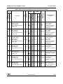
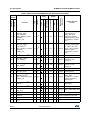
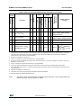
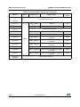
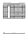
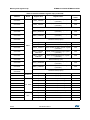
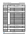
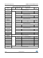
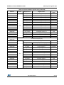
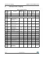
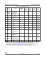
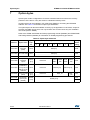
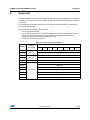
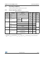
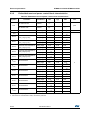
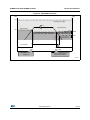
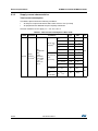
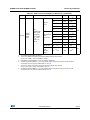
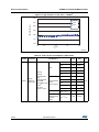
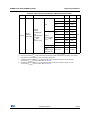
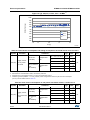
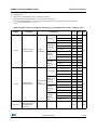
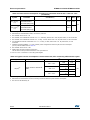
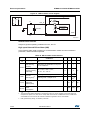
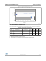
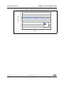
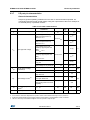
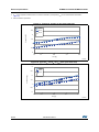
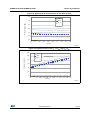
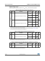
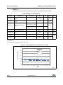
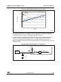
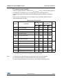
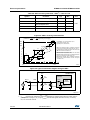
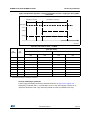
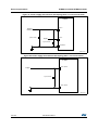
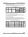
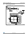
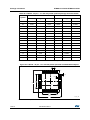
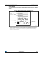
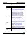
STM8AL313x/4x/6x STM8AL3L4x/6x Electrical parameters Figure 36. Maximum dynamic current consumption on VREF+ supply pin during ADC conversion 6DPSOLQJQF\FOHV &RQYHUVLRQF\FOHV $'&FORFN ,5() $ $ 069 Table 60. RAIN max for fADC = 16 MHz(1) RAIN max (kohm) Ts (cycles) Ts (µs) Slow channels Fast channels 2.4 V < VDDA < 3.6 V 1.8 V < VDDA < 2.4 V 2.4 V < VDDA < 3.3 V 1.8 V < VDDA < 2.4 V 4 0.25 Not allowed Not allowed 0.7 Not allowed 9 0.5625 0.8 Not allowed 2.0 1.0 16 1 2.0 0.8 4.0 3.0 24 1.5 3.0 1.8 6.0 4.5 48 3 6.8 4.0 15.0 10.0 96 6 15.0 10.0 30.0 20.0 192 12 32.0 25.0 50.0 40.0 384 24 50.0 50.0 50.0 50.0 1. Guaranteed by design, not tested in production. General PCB design guidelines Power supply decoupling should be performed as shown in Figure 37 or Figure 38, depending on whether VREF+ is connected to VDDA or not. Good quality ceramic 10 nF capacitors should be used. They should be placed as close as possible to the chip. DocID18474 Rev 6 101/116 105