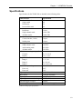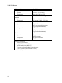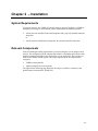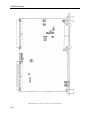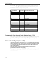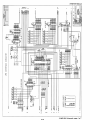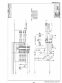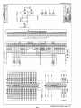
1
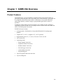
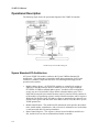
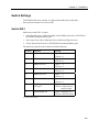
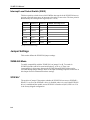
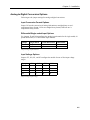
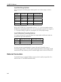
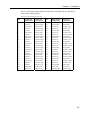
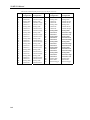
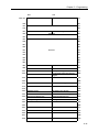
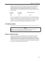
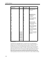
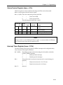
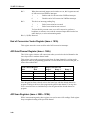
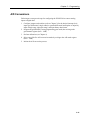
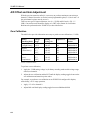
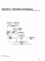
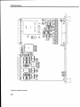
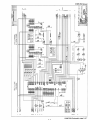
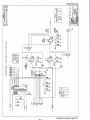
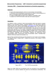
 XVME-564
6U 64/32-Channel Analog Input Module
USER’S MANUAL
ACROMAG INCORPORATED
30765 South Wixom Road
P.O. BOX 437
Wixom, MI 48393-7037 U.S.A.
Tel: (248) 295-0885
Fax: (248) 624-9234
Email: [email protected]
Copyright 2012, Acromag, Inc., Printed in the USA.
Data and specifications are subject to change without notice.
8500-975B Revision
Description
Date
A
B
Manual Released
Manual Updated (incorporates PCN 200)
6/95
10/96
Trademark Information
Brand or product names are registered trademarks of their respective owners.
Windows is a registered trademark of Microsoft Corp. in the United States and other countries.
Copyright Information
This document is copyrighted by Xycom Incorporated (Xycom) and shall not be reproduced or copied
without expressed written authorization from Xycom.
The information contained within this document is subject to change without notice. Xycom does not
guarantee the accuracy of the information and makes no commitment toward keeping it up to date.
Table of Contents
Chapter 1 – XVME-564 Overview ..................................................................................................... 1-1
Product Features ............................................................................................................................. 1-1
Operational Description.................................................................................................................... 1-2
Xycom Standard I/O Architecture .................................................................................................... 1-2
Specifications ................................................................................................................................... 1-3
Chapter 2 – Installation ..................................................................................................................... 2-1
System Requirements...................................................................................................................... 2-1
Relevant Components ..................................................................................................................... 2-1
Switch Settings................................................................................................................................. 2-3
Switch SW-1 ............................................................................................................................ 2-3
Interrupt Level Select Switch (SW-2)....................................................................................... 2-4
Jumper Settings ............................................................................................................................... 2-4
XVME-560 Mode...................................................................................................................... 2-4
SYSFAIL* ................................................................................................................................. 2-4
Analog-to-Digital Conversion Options...................................................................................... 2-5
External Connectors ........................................................................................................................ 2-6
Card Cage Installation...................................................................................................................... 2-9
Chapter 3 – Programming................................................................................................................. 3-1
Flow Charts ...................................................................................................................................... 3-1
Board Initialization Flow Chart ................................................................................................. 3-2
Autoscanning Mode Flow Chart............................................................................................... 3-3
Random Channel Mode Flow Chart......................................................................................... 3-4
External Trigger Mode Flow Chart ........................................................................................... 3-5
Single Channel Mode Flow Chart ............................................................................................ 3-6
Sequential Channel Mode Flow Chart ..................................................................................... 3-7
End-of-Conversion Flow Charts............................................................................................... 3-8
Module Base Addressing ................................................................................................................. 3-9
I/O Interface Block ......................................................................................................................... 3-11
Module Identification Data ..................................................................................................... 3-11
Status/Control Register (base + 81h) .................................................................................... 3-13
Interrupt Timer Register (base + 101h) ................................................................................. 3-13
Programmable Timer Interrupt Vector Register (base + 103h) ............................................. 3-14
Autoscan Control Register (base + 111h).............................................................................. 3-14
A/D Mode Register (base + 180h) ......................................................................................... 3-15
A/D Status/Control Register (base + 181h) ........................................................................... 3-17
End of Conversion Vector Register (base + 183h) ................................................................ 3-18
A/D Gain/Channel Register (base + 184h) ............................................................................ 3-18
A/D Scan Registers (base + 200h - 3FEh) ............................................................................ 3-18
A/D Conversions ............................................................................................................................ 3-19
i
XVME-564 Manual
Chapter 4 – Calibration ..................................................................................................................... 4-1
Programmable Gain Offset Adjustment ........................................................................................... 4-1
A/D Offset and Gain Adjustment...................................................................................................... 4-2
Zero Calibration ....................................................................................................................... 4-2
Full Scale Calibration ............................................................................................................... 4-3
Appendix A – Schematics and Diagrams ........................................................................................A-1
ii
Chapter 1 XVME-564 Overview
Product Features
The XVME-564 is a powerful VMEbus-compatible analog input module capable of
performing analog-to-digital (A/D) conversions with a 16-bit resolution. The module can
be configured to provide 64 single-ended, 32 differential, or 64 pseudo-differential
analog input channels, with three ranges of programmable gain and six modes of
operation.
In addition to offering these powerful capabilities, the XVME-564 offers backward
compatibility with the XVME-560 via a jumper selection. In this mode, the XVME-564
offers 12-bit analog input conversions.
XVME-564 features include
•
64 single-ended, 32 differential, or 64 pseudo-differential 16-bit analog input
channels
•
Unipolar 0-5 V, 0-10 V, or bipolar ±5 V, ±10 V operation
•
Programmable gains of 1, 2, 5,10; 4, 8, 20, 40; or 10, 20, 50, 100
•
16-bit conversion
•
6 operating modes
•
Single channel conversion
•
Sequential channel conversion
•
Random channel conversion
•
External trigger conversion
•
Autoscanning conversion
•
Programming gain
•
10 µsec acquisition and conversion time
•
16 µsec settling time
1-1
XVME-564 Manual
Operational Description
The following figure shows the operational diagram of the XVME-564 module.
XVME-564 Operational Block Diagram
Xycom Standard I/O Architecture
All Xycom XVME I/O modules conform to the Xycom VMEbus Standard I/O
Architecture. This architecture is intended to make the programming of all Xycom
VMEbus I/O modules simple and consistent. The following features apply to the
operation of the module:
1-2
•
Module Address Space – All XVME I/O modules are controlled by writing to
addresses within the 64 Kbyte short I/O address space (or the upper 64 Kbyte
FFXXXXh of VMEbus standard address space). A module can be configured to
occupy any one of 64 available 1 Kbyte blocks within the address space. The 1
Kbyte block occupied by the module (known as the I/O interface block) contains all
of the module’s programming registers, module identification data, and I/O registers.
Within the I/O interface block, the address offsets are standardized so that users can
find the same registers and data at the same address offsets across the entire Xycom
XVME product line.
•
Module Identification – The module has ID information which provides the module
name, model number, manufacturer, and revision level information at a location that
is consistent with other Xycom input modules.
•
Status/Control Register – This register is always located at address module base +
81h, and the lower two bits are standard from module to module.
Chapter 1 – XVME-564 Overview
Specifications
Specifications for the XVME-564 are detailed in the following tables.
Characteristic
Number of channels
Single-ended
Differential
Pseudo-differential
Accuracy
Resolution
Single-channel mode
All other modes
Speed
Conversion time, 16 bits
Settling time
Throughput
Single-channel mode
Autoscanning mode
All other modes
A/D full scale voltage ranges (G=1)
Unipolar
Bipolar
Programmable Gain
Range 1
Range 2
Range 3
Maximum input voltage
Power on
Power off
Input impedance
Bias current
Input capacitance
Operating common mode voltage
External trigger to sample
Power requirements
Specification
64
32
64
16 bits
.003% FSR
.006% FSR
10 µsec
16 µsec
100 KHz
62.5 KHz
38.5 KHz
0-5 V, 0-10 V
±5 V, ±10 V
1, 2, 5, 10
4, 8, 20, 40
10, 20, 50, 100
44 V
30 V
18 M ohm, minimum
±200 pA, maximum
100 pF, maximum
-11 V, +13 V
26 µsec
5 V ±5%, 1.1 A typical
XVME-564 Analog Input Specifications
1-3
XVME-564 Manual
Characteristic
Temperature
Operating
Non-operating
Humidity
Altitude
Operating
Non-operating
Vibration
Operating
Non-operating
Shock
Operating
Non-operating
Specification
0° to 65°C (32° to 149°F)
-40 to 85°C (-40° to 185°F)
5 to 95% RH, non-condensing
Sea level to 10,000 ft. (3048 m)
Sea level to 50,000 ft. (15240 m)
5 to 2000 Hz
.015" peak-to-peak displacement
2.5 g acceleration (maximum)
5 to 2000 Hz
.030" peak-to-peak displacement
5.0 g acceleration (maximum)
30 g peak acceleration,
11 msec duration
50 g peak acceleration
11 msec duration
VMEbus Compliance
A24/16:D16 DTB slave
AM CODES 29, 2D, 39, 3D
BGXIN hardwired to BGXOUT
Conforms to Xycom Standard I/O Architecture
I(1) - I (7) (STAT) (Programmable Vector)
Environmental Specifications
1-4
Chapter 2 – Installation
System Requirements
To operate correctly, the XVME-564 module must be properly installed in a VMEbus
backplane. Following are the minimum system requirements for module operation:
•
A host processor installed in the same backplane and a properly installed controller
subsystem
or
•
A host processor module that incorporates an on-board controller subsystem
Relevant Components
Prior to installing the analog input module, you must configure several jumper/switch
options. The configuration of the jumpers and switches is dependent upon which of the
module operational capabilities are required for a given application. The switches are
used to set VMEbus-related options. The jumper options can be divided into three
categories:
•
VMEbus-related options
•
Analog-to-digital conversion options
The figure on the following page illustrates the jumpers, switches, connectors, and
potentiometers located on the XVME-564.
2-1
XVME-564 Manual
XVME-564 Jumpers, Switches, Connectors, and Potentiometers
2-2
Chapter 2 – Installation
Switch Settings
The XVME-564 has two switches: an eight-position addressing switch and a
three-position interrupt level select switch.
Switch SW-1
Addressing switch SW-1 is used to
•
Select the address on a 1 Kbyte boundary in the VMEbus short I/O or FFXXXXh in
the VMEbus standard address space
•
Select supervisory only or both supervisory and non-privileged accesses
•
Choose between the short I/O or FFXXXXh in the standard address space
The table below describes the switch bits and their functions.
Position
1
Function
Address bit A10
2
Address bit A11
3
Address bit A12
4
Address bit A13
5
Address bit A14
6
Address bit A15
7
Supervisory/nonprivileged
8
Standard/short I/O
Setting
Open = 1
Closed = 0
Open = 1
Closed = 0
Open = 1
Closed = 0
Open = 1
Closed = 0
Open = 1
Closed = 0
Open = 1
Closed = 0
Open = supervisory
Closed = supervisory &
non-privileged
Open = standard access
Closed = short I/O access
Switch SW-1 Bit Settings
2-3
XVME-564 Manual
Interrupt Level Select Switch (SW-2)
This three-position switch selects which VMEbus interrupt level the XVME-564 uses to
generate a periodic interrupt or an interrupt at the end of a conversion. The time period is
determined by the interrupt timer register (base + 101h).
Position 1
Open
Open
Open
Open
Closed
Closed
Closed
Closed
Position 2
Open
Open
Closed
Closed
Open
Open
Closed
Closed
Position 3
Open
Closed
Open
Closed
Open
Closed
Open
Closed
VMEbus Interrupt Level
7
6
5
4
3
2
1
None
Interrupt Level Switch Settings
Jumper Settings
This section defines the XVME-564 jumper settings.
XVME-560 Mode
To enable compatibility with the XVME-560, set jumper J1 to B. To remain in
XVME-564 mode (with all its associated features), set J1 to A. There is an
incompatibility in gain ranges between the XVME-564 and XVME-560 that can be
corrected through jumper settings. Refer to the Input Gain Range Options section later in
this chapter for more information on these settings.
SYSFAIL*
The position of jumper J3 determines whether the XVME-564 can assert a SYSFAIL*.
When J3 is set to A, the SYSFAIL* driver is disabled; when it is set to B the SYSFAIL*
driver is enabled and the module asserts SYSFAIL* when the red (fail) LED is on. J3A
is the factory-shipped configuration.
2-4
Chapter 2 – Installation
Analog-to-Digital Conversion Options
Following are the jumper settings for analog-to-digital conversions.
Input Conversion Format Options
Jumper J62 sets the conversion of analog information to straight binary or two’s
complement binary format. J62A sets straight binary format; J62B sets two’s
complement binary format.
Differential/Single-ended Input Options
Use jumpers J2 and J64 to configure the analog input channels for 64 single-ended, 64
pseudo-differential, or 32 differential input channels.
Jumper
J2
J64
Single-ended
B
A, C
Pseudo-differential
A
A, D
Differential
A
B
Jumper Settings: Input Channels
Input Voltage Options
Jumpers J53, J60, J61, and J63 configure the module for one of four input voltage
ranges.
Jumper
J53
J60
J61
J63
0-5 V
B
A
A
C
0-10 V
B
A
B
A
±5 V
B
A
B
B
±10 V
A
B
A
B
Jumper Settings: Input Voltage
2-5
XVME-564 Manual
Input Gain Range Options
You can program each analog input channel gain for one of three ranges, as shown
below:
Jumper
J54
J55
J56
J57
J58
J59
1, 2, 5, 10
In
Out
Out
In
Out
Out
4, 8, 20, 40
Out
In
Out
Out
In
Out
10, 20, 50, 100
Out
Out
In
Out
Out
In
Jumper Settings: Input Gain Range
Because the XVME-564’s programmable gains of 1, 2, 5, 10 are incompatible with the
XVME-560’s programmable gains of 1, 2, 4, 8, you can achieve gains of 1, 2 using the 1,
2, 5, 10 jumper settings, or gains of 4, 8 using the 4, 8, 20, 40 jumper settings.
Input Calibration Grounding Options
Use jumpers J66 and J67 to ground channel 0 in single-ended or differential mode for
programmable gain offset adjustment.
Jumper
J66
J67
Single-ended Ground
B
A
Differential Ground
B
B
Jumper Settings: Input Calibration Grounding
If you do not want to ground channel 0, jumpers J66 and J67 should be set to A.
In external trigger mode, set J65 IN to pick up digital ground for external trigger signals
returned on JK1 top or bottom, pin 49. If external trigger mode is not used, remove J65.
External Connectors
The XVME-564 uses standard VMEbus connectors for P1 and P2 (96-pin DIN). P2 is
used for extra +5 V and GND connections only.
2-6
Chapter 2 – Installation
JK1 is a dual 50-pin ribbon connector with latches containing 100 pins. Pinouts are
shown in the following tables.
JK1 Pinouts (bottom 50-pin connector)
Pin
1
2
3
4
5
6
7
8
9
10
11
12
13
14
15
16
17
18
19
20
21
22
23
24
25
Single-Ended
Configuration
Channel 0
Channel 8
Analog GND
Channel 9
Channel 1
Analog GND
Channel 2
Channel 10
Analog GND
Channel 11
Channel 3
Analog GND
Channel 4
Channel 12
Analog GND
Channel 13
Channel 5
Analog GND
Channel 6
Channel 14
Analog GND
Channel 15
Channel 7
Analog GND
Channel 16
Differential
Configuration
Channel 0 low
Channel 0 high
Analog GND
Channel 1 high
Channel 1 low
Analog GND
Channel 2 low
Channel 2 high
Analog GND
Channel 3 high
Channel 3 low
Analog GND
Channel 4 low
Channel 4 high
Analog GND
Channel 5 high
Channel 5 low
Analog GND
Channel 6 low
Channel 6 high
Analog GND
Channel 7 high
Channel 7 low
Analog GND
Channel 8 low
Pin
26
27
28
29
30
31
32
33
34
35
36
37
38
39
40
41
42
43
44
45
46
47
48
49
50
Single-Ended
Configuration
Channel 24
Analog GND
Channel 25
Channel 17
Analog GND
Channel 18
Channel 26
Analog GND
Channel 27
Channel 19
Analog GND
Channel 20
Channel 28
Analog GND
Channel 29
Channel 21
Analog GND
Channel 22
Channel 30
Analog GND
Channel 31
Channel 23
Analog GND
Power GND
External trigger
Differential
Configuration
Channel 8 high
Analog GND
Channel 9 high
Channel 9 low
Analog GND
Channel 10 low
Channel 10 high
Analog GND
Channel 11 high
Channel 11 low
Analog GND
Channel 12 low
Channel 12 high
Analog GND
Channel 13 high
Channel 13 low
Analog GND
Channel 14 low
Channel 14 high
Analog GND
Channel 15 high
Channel 15 low
Analog GND
Power GND
External trigger
JK1 Pinouts continued on following page
2-7
XVME-564 Manual
JK1 Pinouts continued from previous page (top 50-pin connector)
Pin
1
2
3
4
5
6
7
8
9
10
11
12
13
14
15
16
17
18
19
20
21
22
23
24
25
2-8
Single-Ended
Configuration
Channel 32
Channel 40
Analog GND
Channel 41
Channel 33
Analog GND
Channel 34
Channel 42
Analog GND
Channel 43
Channel 35
Analog GND
Channel 36
Channel 44
Analog GND
Channel 45
Channel 37
Analog GND
Channel 38
Channel 46
Analog GND
Channel 47
Channel 39
Analog GND
Channel 48
Differential
Configuration
Channel 16 low
Channel 16 high
Analog GND
Channel 17 high
Channel 17 low
Analog GND
Channel 18 low
Channel 18 high
Analog GND
Channel 19 high
Channel 19 low
Analog GND
Channel 20 low
Channel 20 high
Analog GND
Channel 21 high
Channel 21 low
Analog GND
Channel 22 low
Channel 22 high
Analog GND
Channel 23 high
Channel 23 low
Analog GND
Channel 24 low
Pin
26
27
28
29
30
31
32
33
34
35
36
37
38
39
40
41
42
43
44
45
46
47
48
49
50
Single-ended
Configuration
Channel 56
Analog GND
Channel 57
Channel 49
Analog GND
Channel 50
Channel 58
Analog GND
Channel 59
Channel 51
Analog GND
Channel 52
Channel 60
Analog GND
Channel 61
Channel 53
Analog GND
Channel 54
Channel 62
Analog GND
Channel 63
Channel 55
Analog GND
Power GND
External Trigger
Differential
Configuration
Channel 24 high
Analog GND
Channel 25 high
Channel 25 low
Analog GND
Channel 26 low
Channel 26 high
Analog GND
Channel 27 high
Channel 27 low
Analog GND
Channel 28 low
Channel 28 high
Analog GND
Channel 29 high
Channel 29 low
Analog GND
Channel 30 low
Channel 30 high
Analog GND
Channel 31 high
Channel 31 low
Analog GND
Power GND
External Trigger
Chapter 2 – Installation
Card Cage Installation
Caution
Do not attempt to install or remove any boards without first turning off power to the
bus and all related external power supplies.
Prior to installing a module, determine and verify all relevant jumper configurations.
Check the jumper configuration with the diagram and lists in the manual.
Xycom VMEbus modules can accommodate typical VMEbus backplane construction.
The following illustration depicts a standard VMEbus chassis and a typical backplane
configuration. There are two rows of backplane connectors depicted (the P1 and the P2
backplane).
2-9
XVME-564 Manual
Perform the following steps to install a board in the card cage:
1. Make sure the card cage slot that you are going to use is clear and accessible.
2. Center the board on the plastic guides in the slot so that the handle on the front panel
is toward the bottom of the card cage.
3. Push the card slowly toward the rear of the chassis until the connectors are fully
engaged and properly seated.
Note
It should not be necessary to use excess force to engage the connectors. If the board
does not properly connect with the backplane, remove the module and inspect all
connectors and guide slots for possible damage or obstructions.
4. Once the board is properly seated, tighten the two machine screws at the top and
bottom of the front panel.
2-10
Chapter 3 – Programming
This chapter provides the information required to program the XVME-564 for analog
input signal conversions. This information includes the following:
•
Flow charts providing quick-start information
•
Module address map showing programming locations
•
Base addressing and the module I/O interface block
•
A/D conversion modes
Flow Charts
The following flow charts provide information on initializing the XVME-564 board,
using A/D conversion modes, and detecting the end of a conversion. The flow charts
assume that hardware jumpers have been set. See Chapter 2 for information on setting
jumpers.
Note
Register information begins on page 3-13.
3-1
XVME-564 Manual
Board Initialization Flow Chart
This flow chart describes the steps necessary to initialize the XVME-564.
3-2
Chapter 3 – Programming
Autoscanning Mode Flow Chart
In autoscanning mode, continuous conversions are performed on 8, 16, 32, or
64 channels, and the results of each channel are stored in 16-bit registers, starting at
offset base + 200h for channel 0 to base + 27Fh for channel 63.
3-3
XVME-564 Manual
Random Channel Mode Flow Chart
In random channel mode, a control byte written to the low byte of the gain/channel
register that specifies a channel automatically starts a conversion on that channel.
3-4
Chapter 3 – Programming
External Trigger Mode Flow Chart
In external trigger mode, the rising edge of a low-going, externally triggered pulse (on
pin 50 of JK1)–referenced to power ground (pin 49 of JK1, J65IN)–initiates a
conversion.
Note
J65 must be IN to use this mode. See Chapter 2 for information on jumper settings.
3-5
XVME-564 Manual
3-6
Chapter 3 – Programming
Single Channel Mode Flow Chart
In single channel mode, the module automatically starts another conversion on the
specified channel after the low order A/D register (base + 187h) has been read.
3-7
XVME-564 Manual
Sequential Channel Mode Flow Chart
In sequential channel mode, the module automatically increments the channel number by
one and initiates a conversion on the next channel (previous channel + 1) after the low
byte A/D register (base + 187h) has been read.
3-8
Chapter 3 – Programming
End-of-Conversion Flow Charts
3-9
XVME-564 Manual
Module Base Addressing
The XVME-564 is designed to be addressed within either the VMEbus-defined 64 Kbyte
short I/O address space or the upper 64 Kbytes of the standard address space (FF0000hFFFC00h). Because each I/O module connected to the bus must have a unique base
address, the addressing scheme for Xycom XVME I/O modules is configurable. When
the XVME-564 is installed in a system, it will occupy a 1 Kbyte block of address space
(also referred to as the I/O block).
The base address decoding scheme for the XVME-564 positions the starting address of
each board on a 1 Kbyte boundary. Thus, there are 64 possible base addresses (1 Kbyte
boundaries) for the XVME-564 within either the short I/O address space or the upper
64 Kbytes of standard address space. (Refer to Chapter 2 for a list of base addresses and
their corresponding SW-1 bit locations.)
3-10
Chapter 3 – Programming
Base +00h
Even
Odd
Undefined
Module Identification
+3Eh
01h
3Fh
+40h
Reserved
+7Eh
41h
7Fh
+80h
Status/Control Register
+82h
Undefined
81h
83h
+86h
87h
+88h
89h
+8Ah
8Bh
+8Ch
8Dh
+8Eh
8Fh
+90h
Reserved
91h
+92h
93h
+94h
95h
+96h
97h
+98h
99h
+E6h
E7h
+E8h
E9h
+EAh
EBh
+100h
Interrupt Timer Register
101h
+102h
Programmable Timer Interrupt Vector
Register
103h
+104h
105h
+108h
109h
+110h
Autoscan Control Register
111h
+112h
113h
+178h
179h
+180h
A/D Mode Register
+182h
A/D Status/Control Register
181h
End of Conversion Vector Register
183h
+184h
Gain/Channel Register High
Gain/Channel Register Low
185h
+186h
A/D Register High
A/D Register Low
187h
+188h
189h
+198h
199h
+200h
Channel 0 A/D Scan
Channel 0 A/D Scan
201h
+202h
Channel 1 A/D Scan
Channel 1 A/D Scan
203h
+204h
Channels 2-62 A/D Scan
Channels 2-62 A/D Scan
205h
+27Ch
+27Eh
27Dh
Channel 63 A/D Scan
Channel 63 A/D Scan
27Fh
3-11
XVME-564 Manual
XVME-564 Memory Map
3-12
Chapter 3 – Programming
Any location within the XVME-564’s 1 Kbyte I/O interface block can be accessed by
adding the module base address to the address of the specific location within the I/O
interface block (referred to as the I/O interface block offset). For example, the
status/control register is located at address 81h within the I/O interface block. If the
module base address is set at 1000h, then the status/control register would be accessible
at address 1081h.
Module Base
Address
1000h
I/O Interface
Block Offset
+
081h
Status/Control Register
=
1081h
For memory-mapped CPU modules, the short I/O address space is memory mapped to
begin at a specific address. For such modules, the I/O interface block offset is an offset
from the start of this memory-mapped short I/O address space. For example, if the short
I/O address space of a CPU module starts at F90000h and if the base address of the
module is set at 1000h, the actual module base address would be F91000h.
I/O Interface Block
This section describes the programming locations in the XVME-564 I/O interface block.
Note
Reading from or writing to undefined I/O interface block locations may make
application software incompatible with future XVME modules.
Module Identification Data
The Xycom module identification scheme provides a unique method of registering
module-specific information in an ASCII-encoded format. ID data is provided as
32 ASCII encoded characters consisting of the board type, manufacturer identification,
module model number, number of 1 Kbyte blocks occupied by the module, and module
functional revision level. This information can be read by the system processor on power
up to verify the system configuration and operational status. The table on the following
page defines the identification information locations.
3-13
XVME-564 Manual
Offset Relative to
a Module Base
Contents
1
3
5
7
9
V
M
E
I
D
ASCII Encoding
(hexadecimal)
56
4D
45
49
44
B
D
F
X
Y
C
58
59
43
11
13
15
17
19
1B
1D
5
6
4
35
36
34
20
20
20
20
1F
1
31
21
23
1
20
31
Major functional revision
level with leading blank
(if single digit)
31
20
Minor functional revision
level with trailing blank (if
single digit)
25
27
1
29
2B
2D
2F
31
33
35
37
39
3B
3D
3F
Reserved
Reserved
Reserved
Reserved
Reserved
Reserved
Reserved
Reserved
Reserved
Reserved
Reserved
Reserved
Description
ID PROM identifier;
always VMEID (five
characters)
Manufacturer’s ID,
always XYC for Xycom
modules (three
characters)
Module Model Number
(three characters, four
trailing blanks)
Number of 1 Kbyte
blocks of I/O space
occupied by this module
(one character)
Manufacturer-dependent
information; reserved for
future use
Identification Data
The module has been designed so that it is only necessary to use odd backplane
addresses to access the ID data. Thus, each of the 32 bytes of ASCII data have been
assigned to the first 32 odd I/O interface block bytes (that is, odd bytes 1h-3Fh).
ID information can be accessed by addressing the module base, offset by the specific
address for the character(s) needed. For example, if the base address of the board is
jumpered to 1000h, and if you wish to access the module model number (I/O interface
block locations 11h, 13h, 15h, 17h, 19h, 1Bh, and 1Dh), individually add the offset
addresses to the base addresses to read the hex-encoded ASCII value at each location.
Thus, in this example, the ASCII values that make up the module model number are
found sequentially at locations 1011h, 1013h, 1015h, 1017h, 1019h, 101Bh, and 101Dh.
3-14
Chapter 3 – Programming
Status/Control Register (base + 81h)
This 8-bit register is used to control the red and green LEDs used on the module.
Below is a description of the bits in this register:
Bits 1, 0 (LSB) These bits control the green and red LEDs.
1
=
Turns on red LED
0
=
Turns on green LED
The following table defines bits 1 and 0.
Status Bits
1
0
0
0
LEDs
Green
Off
Red
On
SYSFAIL*
On
0
1
1
Off
On
On
Off
On
Off
Off
Off
Off
1
0
1
Status
Module failed, or not yet
tested
Inactive module
Module undergoing test
Module passed test
Note
Whenever bit 0 is 0, the VMEbus SYSFAIL* signal is asserted, and the red LED turns
on. The power-up or reset state for status bits is 00.
Interrupt Timer Register (base + 101h)
The 8-bit interrupt timer register generates VMEbus interrupts with configurable delay
times. It has the following bit definitions:
Bit 7 (MSB)
Bit 6
Bits 5-3
Depending on jumper and switch settings, this bit enables or disables
periodic VMEbus interrupts.
1
=
Enables periodic interrupts
0
=
Disables periodic interrupts
This period select bit selects the time interval for a one-bit change in
delay bits.
1
=
Delay bit time interval is 131.072 msec
0
=
Delay bit time interval is 8.192 msec
Reserved
3-15
XVME-564 Manual
Bits 2-0 (LSB) These period multiplier bits select a timeout period for the interrupt
timer. The resolution for each bit is determined by the delay set bit.
The table below defines the interrupt timeout periods.
Period Multiplier
Bits
000
001
010
011
100
101
110
111
000
001
010
011
100
101
110
111
Period Select
Bit
0
0
0
0
0
0
0
0
1
1
1
1
1
1
1
1
Interrupt Timeout Period
8.192 msec
16.384 msec
24.576 msec
32.768 msec
40.960 msec
49.152 msec
57.344 msec
65.536 msec
131.072 msec
262.144 msec
393.216 msec
524.288 msec
655.360 msec
786.432 msec
917.504 msec
1048.576 msec or 1.048 sec
Interrupt Timeout Periods
Programmable Timer Interrupt Vector Register (base + 103h)
This read/write register holds the vector to be driven on the VMEbus when the interrupt
generated by the interrupt timer is acknowledged. This register clears on power up.
Autoscan Control Register (base + 111h)
Continuous conversions are performed on 8, 16, 32, or 64 channels when autoscanning
mode is selected (that is, base + 180h is set to 4). The results of each channel are stored
in a 16-bit register (using dual-ported RAM) starting at offset 200h (channel 0) and
ending at 2Fh (channel 63).
In this mode, end of A/D conversion interrupts cannot be used; however, the
programmable interrupt timer is still available.
This register clears on power up or SYSRESET*. Bit 7 can also be cleared by an A/D
section software reset.
3-16
Chapter 3 – Programming
The bits in this register are defined below:
Bit 7 (MSB)
Bits 6-2
This bit enables or disables the autoscan control register. It is cleared on
power up, SYSRESET*, or A/D software reset.
1
=
Autoscanning enabled
0
=
Autoscanning disabled
Reserved
Bits 1, 0 (LSB) These bits, defined in the table below, are used to select the channels to
be scanned. These bits are cleared on power up or SYSRESET*.
Scan Select Bits
Bit 1 Bit 0
0
0
0
1
1
0
1
1
Channels Scanned
0-7
0-15
0-31
0-64
A/D Mode Register (base + 180h)
This 8-bit register determines the operating mode for the analog inputs used on the
module. The bits are defined below:
Bits 15 (MSB) -11
Reserved
Bit 10
Mode bit 2
Bit 9
Mode bit 1
Bit 8 (LSB)
Mode bit 0
The mode bits determine the operating mode for analog inputs. One of six modes can be
selected, as defined in the table below:
Mode Bits
Bit 2
Bit 1
0
0
0
0
0
1
0
1
1
0
1
0
Bit 0
0
1
0
1
0
1
A/D Conversion Mode
Single channel
Sequential channel
Random channel
External trigger
Autoscanning
Programming gain
3-17
XVME-564 Manual
The A/D conversion modes are described below.
Single Channel Mode
In single channel mode, the module automatically starts another conversion on the
specified channel after the low byte of the A/D register (base + 187h) has been read. An
added feature of the single channel mode is that it offers faster conversions than the other
modes (10 µsec as opposed to 26 µsec in sequential, random channel, and external
trigger modes, and 18 µsec in autoscanning mode).
Sequential Channel Mode
In sequential channel mode, the module automatically increments the channel number by
one and initiates a conversion on the next channel (previous channel + 1), after the low
byte of the A/D register (base + 187h) has been read. You can force a conversion in this
mode without incrementing the channel number by writing a 1 to bit 7 of the
status/control register (base + 181h).
Random Channel Mode
In random channel mode, a control byte written to the low byte of the gain/channel
register (base + 184h) that specifies a channel number automatically starts a conversion
on the specified channel.
External Trigger Mode
External trigger mode allows the rising edge of a low-going, externally triggered pulse
(on pin 50 of JK1)–referenced to power ground (pin 49 of JK1, J65IN)–to initiate a
conversion.
Autoscanning Mode
Autoscanning mode performs continuous conversions on 8, 16, 32, or 64 channels, and
stores the results of each channel in its own 16-bit register starting at offset base + 200h
(channel 0) to base + 27Fh (channel 63). When autoscanning mode is selected and bit 7
of the autoscan control register is set to 1, conversions are initiated and stored. End of
A/D conversion interrupts cannot be used with this mode and will not generate
interrupts. However, the programmable interrupt timer is available.
Programming Gain Mode
After power up or system reset, use this mode to initialize the XVME-564’s on-board
gain RAM to provide each input channel with an associated gain factor from the jumperselectable range set at installation. Once an input channel is initialized, the associated
gain factor is automatically applied when an A/D conversion occurs on that channel.
To program the gain RAM, first select programming gain mode. Once this mode is set,
you can write the gain for each channel to the high byte of the gain/channel register (base
+ 184h). Refer to the A/D Gain/Channel Register section later in this chapter for more
information on programming the gain RAM.
3-18
Chapter 3 – Programming
A/D Status/Control Register (base + 181h)
This 8-bit register is used to monitor the status of A/D channels, enable and disable
interrupts, and reset the module. The bits in this register are defined below:
Bit 7 (MSB)
Bit 6
This bit acts as a busy flag to show when an A/D conversion is in
progress.
1
=
A/D conversion in process
0
=
No conversion in process
This bit initiates a conversion. The length of the conversion is dependent
upon which of the six A/D modes the board is operating.
1
=
Conversion initiated
0
=
No conversion initiated
Bit 5
Reserved
Bit 4
This bit is used to perform an analog input section software reset. A
software reset stops a conversion in process and clears any end-ofconversion interrupts. It also clears the interrupt pending flag (bit 2),
resets the gain/channel register (base + 184h), and disables scanning by
clearing the scan control bit (bit 7 of base + 111h).
1
=
Starts the software reset process
0
=
Stops the reset
3-19
XVME-564 Manual
Bit 3
Bit 2
When the associated jumpers and switches are set, this bit generates end
of A/D conversion VMEbus interrupts.
1
=
Enables end of A/D conversion VMEbus interrupts
0
=
Disables end of A/D conversion VMEbus interrupts
This bit is an interrupt pending flag.
1
=
End of conversion has occurred
0
=
End of conversion has not occurred
To clear this bit you must cause a new A/D conversion, perform a
backplane or software reset, read the converted input data from the low
order data byte, or select autoscanning mode.
Bits 1, 0 (LSB) Reserved
End of Conversion Vector Register (base + 183h)
This register stores the vector used for end of A/D conversion interrupts.
A/D Gain/Channel Register (base + 184h)
This 16-bit register initiates A/D conversions when you write the desired channel to the
lower byte while in random channel mode.
This register is also used to program a gain factor for input channels by writing to the
higher byte while in programming gain mode. Use bits 8 and 9 to first select the gain, as
shown in the table below.
Gain/Channel Register
Bit 9
Bit 8
0
0
0
1
1
0
1
1
Jumper-Selected Gain
Range 1
Range 2
1
4
2
8
5
20
10
50
Range 3
10
20
50
100
Once the gain has been selected, write to the lower byte with the desired channel to
program. Writing to the lower byte programs the gain for that channel. You may also
write a word at a time to simultaneously select the gain and the desired channel to
program.
A/D Scan Registers (base + 200h - 3FEh)
While in autoscanning mode, these registers are used to store A/D readings. Each register
keeps an updated reading of the specified channel.
3-20
Chapter 3 – Programming
A/D Conversions
Following are some general steps for configuring the XVME-564 to convert analog
inputs to digital data:
1. Configure jumpers and switches (refer to Chapter 2) for the desired interrupt level,
input type (differential, single-ended, or pseudo-differential and bipolar or unipolar),
input voltage range, input gain range, and input binary data format.
2. Program the gain RAM by setting programming gain mode, then writing to the
gain/channel register (base + 184h).
3. Perform calibration (see Chapter 4).
4. Select one of the five A/D conversion modes by writing to the A/D mode register
(base + 180h).
5. Initiate the A/D conversion process.
3-21
Chapter 4 – Calibration
Calibration facilities have been provided on the module for analog circuits. The module
is calibrated in the ±10 V A/D input voltage before it leaves the factory. However, if the
module is configured to operate in ranges other than these, it is recommended that the
calibration be checked and adjusted. As a general rule, the input circuitry should be
recalibrated whenever voltage range jumpers and voltage/current select jumpers are
changed.
Resistor Number
R69
R70
R76
Type of Adjustment
Offset for A/D convertor
Gain for input circuit
Programmable gain amp offset
A/D Calibration Potentiometers
Input circuit calibration entails offset nulling the instrumentation amplifier, and offset
adjusting and gain adjusting the A/D converter.
You will need the following equipment to perform an input calibration:
•
Five-digit volt meter capable of reading ±30 µV
•
Small flat-bladed screw driver
•
Precision voltage source capable of supplying 1.22 mV ±30 µV
Inputs can be calibrated in either single-ended or differential configuration. Calibration
begins by offset nulling the instrumentation amplifier with channel 0 selected and its
inputs grounded.
Programmable Gain Offset Adjustment
Perform the following steps to adjust the programmable gain offset for single-ended,
unipolar operation:
1. Remove any connectors at JK1.
2. Ground input channel 0 by setting jumper J66 to B.
3. Measure and record the output voltage of gain amp U39, pin 6 using the Fluke 8860
DMM.
4. Next, measure the voltage of gain amp U37, pin 6.
5. Adjust R76 so the output voltage of U37, pin 6 matches the output voltage of U39,
pin 6.
6. Reset jumper J66 to A for the rest of the calibration.
4-1
XVME-564 Manual
A/D Offset and Gain Adjustment
With the previous networks nulled, it is necessary to perform continuous conversion on
channel 0. Channel 0 must be set for the lowest programmable gain (G=1; bits 6 and 7 of
the gain/channel register must be set to 0).
There are two types of input calibration: zero (0 + .5 LSB) and full scale (+FS - 1.5
LSB). Conversion results should be display on a CRT in hex format for verification.
Both must be performed on the XVME-564, as described below.
Zero Calibration
The table below provides information necessary to perform a zero calibration (+.5 LSB).
Binary
Encoding Mode
Unipolar
(straight binary)
Bipolar
(offset binary)
Bipolar
(two’s
complement)
Voltage
Range
0-5 V
0-10 V
±2.5 V
±5 V
±10 V
±2.5 V
±5 V
±10 V
Analog
Voltage In
.04 mV
.08 mV
.04 mV
.08 mV
.15 mV`
.04 mV
.08 mV
.15 mV`
Adjust POT
R69
R69
R69
R69
R69
R69
R69
R69
Transition
Points
0000h/0001h
0000h/0001h
8000h/8001h
8000h/8001h
8000h/8001h
0000h/0001h
0000h/0001h
0000h/0001h
A/D Zero Calibration Points
To perform a zero calibration,
1. Apply the .5 LSB analog voltage in (for binary encoding mode and the voltage range
chosen) to channel 0.
2. Adjust the zero calibration and the POT until the display reading toggles between the
zero calibration and transition point values.
For example, to perform a zero calibration on an XVME-564 configured for bipolar,
offset binary, ±10 V range operation,
4-2
•
Apply +.15 mV to channel 0
•
Adjust R69 until the display reading toggles between 0000h and 0001h
Chapter 4 – Calibration
Full Scale Calibration
The table below provides information necessary to perform a full scale calibration (+FS 1.5 LSB).
Binary
Encoding Mode
Unipolar
(straight binary)
Bipolar
(offset binary)
Bipolar
(two’s
complement)
Voltage
Range
0-5 V
0-10 V
±2.5 V
±5 V
±10 V
±2.5 V
±5 V
±10 V
Analog
Voltage In
4.99988 V
9.99977 V
2.49988 V
4.99977 V
9.99954 V
2.49988 V
4.99977 V
9.99954 V
Adjust POT
R70
R70
R70
R70
R70
R70
R70
R70
Transition
Points
FFFEh/FFFFh
FFFEh/FFFFh
FFFEh/FFFFh
FFFEh/FFFFh
FFFEh/FFFFh
7FFEh/7FFFh
7FFEh/7FFFh
7FFEh/7FFFh
A/D Full Scale Calibration Points
To perform a full scale calibration,
1. Apply the analog voltage in (for binary encoding mode and the voltage range chosen)
to channel 0.
2. Adjust the full scale calibration and the POT until the display reading toggles
between the full scale calibration and transition point values.
For example, to perform a full scale calibration on an XVME-564 configured for bipolar,
offset binary, ±10 V range operation,
•
Apply +9.99954 V to channel 0
•
Adjust R70 until the display reading toggles between FFFEh and FFFFh
4-3
Index
A
E (continued)
A/D calibration potentiometers, 4-1
A/D conversion modes
autoscanning, 3-16
external trigger, 3-16
programming gain, 3-16
random channel, 3-16
sequential channel, 3-16
single channel, 3-16
A/D conversions, 3-19
A/D mode register, 3-15
A/D offset and gain adjustment, 4-2
A/D gain/channel register, 3-18
A/D scan registers, 3-18
A/D status/control register, 3-17
analog input
features, 1-1
specifications, 1-3
analog-to-digital conversion options, 2-5
differential/single-ended input options, 2-5
input calibration grounding, 2-6
input conversion format, 2-5
input gain range options, 2-6
input voltage, 2-5
assembly drawing, A-2
autoscan control register, 3-14
autoscanning mode, 3-3, 3-16
external connectors, 2-6
external trigger mode, 3-5, 3-16
B
block diagram, 1-2, A-2
board initialization, 3-2
board overview, 1-1
C
cabling, 2-7
calibration, 4-1
card cage installation, 2-9
chassis, VMEbus, 2-9
connectors, external, 2-6
conversion, A/D, 3-19
E
end of conversion flow charts, 3-8
end of conversion vector register, 3-18
environmental specifications, 1-4
F
features, analog input, 1-1
flow charts
autoscanning mode, 3-3
board initialization, 3-2
end of conversion, 3-8
external trigger mode, 3-5
random channel mode, 3-4
sequential channel mode, 3-7
single channel mode, 3-6
H
host processor, 2-1
I
I/O interface block, 3-11
initialization, board, 3-2
input calibration grounding options, 2-6
input conversion format options, 2-5
input gain range options, 2-6
input voltage options, 2-5
installation, into a card cage, 2-9
interrupt timer register, 3-13
J
JK1 connector pinouts, 2-7
jumper settings, 2-4
M
memory map, 3-10
modes
autoscanning, 3-16
external trigger, 3-16
programming gain, 3-16
random channel, 3-16
sequential channel, 3-16
single channel, 3-16
module base addressing, 3-9
module identification data, 3-11
I-1
XVME-564 Manual
O
operational diagram, 1-2
options, analog-to-digital conversions, 2-5
P
potentiometers, A/D calibration, 4-1
programming gain mode, 3-16
programmable gain offset adjustment, 4-1
programmable timer interrupt vector register, 3-14
R
random channel mode, 3-4, 3-16
registers
A/D, 3-18
A/D mode, 3-15
autoscan control, 3-14
end of conversion vector, 3-18
interrupt timer, 3-13
programmable timer interrupt vector, 3-14
requirements, system, 2-1
S
schematics, A-3
sequential channel mode, 3-7, 3-16
settings
jumper, 2-4
switch, 2-3
single channel mode, 3-6, 3-16
specifications
analog input, 1-3
environmental, 1-4
standard I/O architecture, 1-2
switch settings, 2-3
switches
interrupt level select, 2-4
SW-1, 2-3
system requirements, 2-1
V
VMEbus chassis, 2-9
I-2