1
Microcontroller Programming
LMP1: Introduction to µController programming
Laboratory LPM1 – Example based introduction to µController programming
Objectives
-
To learn about typical elements common to most modern microcontrollers
To introduce the Keil development environment for Infineon microcontrollers as a
tool for a simulation based microcontroller programming
To create a simple project and learn how to debug it in simulation mode
To explore the C167CR information data base and sample programs
Introduction
The Infineon C166 is a family of 16-bit microcontrollers which has become a popular
platform in the automotive industry. Originally designed in the early 90s by Siemens
Semiconductors (now: Infineon Technologies, www.infineon.com) the C166 family has
quickly grown and currently includes the following members: C161, C163, C164, C165
and C167. The various members of this family differ in the amount of on-chip RAM
and/or ROM, as well as in the number of peripheral elements including the Digital
Input/Output (DIO) channels, the Analog-to-Digital Converters (ADC), the Pulse-Width
Modulation (PWM) units, the General Purpose Timers (GPT), event counters (capture
and compare, CAPCOM) and communication interfaces for synchronous serial
communication (SSC), asynchronous serial communication (ASC), Controller-AreaNetwork (CAN) bus based communication, etc.
Many of these peripheral elements are fairly standard to most modern microcontrollers.
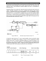
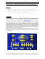
The diagram shown in Figure LMP1-1 outlines the structure of the Infineon C167CR
microcontroller.
Figure LMP1-1
The C167CR microcontroller
Notice how RAM, ROM and all peripheral units are connected to the computational
C166-core via a common address and data bus (Von-Neumann architecture). The
1
Microcontroller Programming
LMP1: Introduction to µController programming
external bus controller is a gateway to the optional external address and data bus,
providing the microcontroller with access to externally connected peripherals (e.g.
external memory, etc.). The computational core comprises the central processing unit
(CPU), an interrupt controller as well as a special Peripheral Event Controller (PEC,
not used in this exercise).
A number of programming environments are available for this microcontroller family. In
this exercise we will use Keil µVision, an Integrated Development Environment (IDE)
which includes a powerful simulator of C166 based microcontrollers. A code-size
limited evaluation version of the Keil development tool chain can be obtained free of
charge from www.keil.com.
1.
Creating a new project
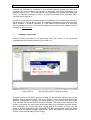
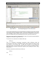
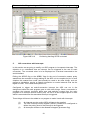
Launch the IDE by clicking on the Start menu entry Keil uVision 2. You should be
presented with the following screen (Figure LMP1-2):
Figure LMP1-2
The Keil IDE µVision 2 (start-up screen)
The main window of the IDE is split into 3 areas: On the left-hand side you can see the
(possibly empty) project browser. This is an ‘Explorer’ type reference window through
which all components of a project can be accessed, e. g. the source files, library files
to be included and the online documentation (Books). The window at the bottom of the
screen will present you with useful information about the compilation process (Build),
error messages, etc. Finally, the large central area of the screen is where you are
going to develop and debug your programs. The IDE automatically opens the latest
project (here: the sample program ‘hello world’). Close this project by pulling down the
‘Project’ menu and selecting ‘Close Project’.
2
Microcontroller Programming
LMP1: Introduction to µController programming
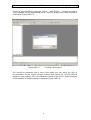
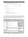
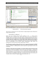
Create an empty project by choosing ‘Project → New Project…’. Change the path to
your workspace on the departmental server. Save the empty project using ‘myProject’
as filename (Figure LMP1-3).
Figure LMP1-3
Creating a new project
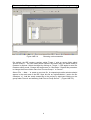
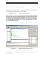
You should be presented with a menu from which you can select the type of
microcontroller for this project. Choose Infineon then select the C167CR-LM (LM
stands for ‘less memory’; this is the ROM-less version of the C167). A brief summary
of the available on-chip peripherals is displayed (Figure LMP1-4)
3
Microcontroller Programming
Figure LMP1-4
LMP1: Introduction to µController programming
Choosing a microcontroller
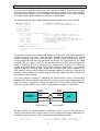
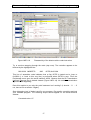
Per default, the IDE creates a project called ‘Target 1’ with an empty folder called
‘Source Group 1’. You can modify these names in the same way you would modify a
filename in explorer. Select the target by clicking on ‘Target 1’. Click again to enter the
filename editing mode. Change the target name to ‘Simulation’. Repeat this procedure
to change the source folder name from ‘Source Group 1’ to ‘Source’.
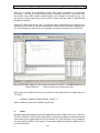
Select ‘File → New…’ to create a new text file. A notepad style editor window should
appear in the work area of the IDE. Save this file as ‘myHelloWorld.c’ (notice the file
extension ‘.c’). Add the newly created file to the project by right-hand clicking on the
group folder ‘Source’ and selecting ‘Add Files to Group Source…’ (Figure LMP1-5).
4
Microcontroller Programming
LMP1: Introduction to µController programming
Figure LMP1-5
Adding a file to the project
This concludes the creation of a new project. We are now ready to write a simple Cprogram for the C167CR microcontroller and test it using the µVision simulator.
2.
A simple ‘Hello world’ program
Most introductions to high-level programming languages begin with a simple program
displaying the message ‘Hello world’ on the standard output (usually, the screen of the
monitor). With microcontrollers, however, things are slightly more complicated: In
contrast to a personal computer (PC), a microcontroller does not have a dedicated
standard output. The habitual C-commands ‘printf’ and ‘scanf’ can therefore not be
used in the same way as on a PC.
A microcontroller program can display information by changing the logic levels (high,
low) of its digital I/O pins. Connecting a logic probe (LED, oscilloscope, etc.) these
levels can be made visible to an external observer. Such a single-bit display is usually
limited to true/false statements such as ‘program has reached line X’ or ‘A/D
conversion complete’. Slightly more flexibility arises from combining n digital I/O lines
to an n-bit binary coded word. The value of this data word can then be displayed using
n LEDs, a 7-segment display or an LCD display.
Most frequently, however, the microcontroller is connected to a host computer through
a serial or parallel cable. Using serial communication and a terminal program, the
microcontroller can be provided with a standard output channel similar to that of a PC
(e.g. the currently active window on the screen). The output of C-commands such as
‘printf’ and ‘putc’ is re-directed to the serial interface, thereby allowing a developer to
display information on the screen of the host computer. Many software development
5
Microcontroller Programming
LMP1: Introduction to µController programming
environments for microcontrollers ship with customized ANSI-C libraries which readily
implement this re-direction of the standard input/output channel to the serial interface.
All a programmer needs to do is to configure the serial interface of the microcontroller
for communication at the desired line speed (e.g. 57600 bits/s).
The following short program demonstrates how this can be done on the C167CR:
#include <stdio.h>
#include <reg167.h>
/* standard I/O header file (printf) */
/* special function registers of the C167 */
/****************/
/* main program */
/****************/
void main(void) {
/* initialize the serial interface
*/
DP3 |= 0x0400;
/* PORT 3.10 DIRECTION CONTROL: OUTPUT (TXD) */
DP3 &= ~0x0800;
/* PORT 3.11 DIRECTION CONTROL: INPUT (RXD) */
P3
|= 0x0400;
/* PORT 3.10 DATA: HIGH (LINE IDLE) */
S0TIC = 0x80;
/* SET TRANSMIT INTERRUPT FLAG (TX COMPLETE) */
S0RIC = 0x00;
/* CLEAR RECEIVE INTERRUPT FLAG (NOTHING REC.) */
S0BG = 0x40;
/* SET BAUDRATE TO 9600 BAUD */
S0CON = 0x8011;
/* SET SERIAL MODE */
/* display 'hello world' */
printf("Hello World\n");
/* endless loop to stop program from running into void */
while(1) {}
}
The program includes two header files, stdio.h and reg167.h. The former provides a
function prototype for ‘printf’, while the latter contains the definition of all special
function registers (SFR) of the microcontroller. Special function registers are used to
control peripheral units such as the digital I/O drivers, the A/D converter, the serial
interface (S0), etc. When written to, the individual bits of an SFR often configure the
mode of operation of such a peripheral unit. Reading the contents of an SFR can
provide information about a unit’s current state. Example: Setting bit 7 in the control
register of the A/D converter (ADC) triggers a conversion cycle. Upon completion, the
ADC sets bit 6 of the control register (and possibly triggers an interrupt). Polling bit 6 of
the ADC control register can thus be used to determine whether the A/D conversion is
still ongoing or has finished.
The main program begins by initialising the asynchronous serial communication
interface (S0). Communication with the host is done using a simple null-modem. This
type of connection consists of a three wire cable with lines for receive (RXD), transmit
(TXD) and ground (GND). Figure LMP1-6 demonstrates this type of connection.
HOST
TXD
TXD
RXD
RXD
GND
Figure LMP1-6
µC
Null-modem
On the C167CR, the serial interface is connected to port 3, pin 10 (TXD) and pin 11
(RXD). We therefore have to ensure that P3.10 is configured as output, whereas P3.11
needs to be set-up as input. This is achieved by the following two lines:
DP3
DP3
|= 0x0400;
&= ~0x0800;
/* PORT 3.10 DIRECTION CONTROL: OUTPUT (TXD) */
/* PORT 3.11 DIRECTION CONTROL: INPUT (RXD) */
6
Microcontroller Programming
LMP1: Introduction to µController programming
DP3 is the (16-bit) data direction register of port 3. Setting a bit (→ 1) in DP3
configures the corresponding signal pin as output; re-setting a bit (→ 0) ensures that
the corresponding pin is switched onto the input driver. The above lines set bit 10 of
DP3 while bit 11 is reset to zero. Recall that
DP3 |= 0x0400;
is short for
DP3 = DP3 | 0x0400;
/* binary OR */
and that the operator ‘|’ stands for binary OR. The hexadecimal value 0x0400 can be
interpreted as binary 0000.0100.0000.0000, i. e. bit 10 is set whereas all other bits are
zero. This value is called a positive mask for bit 10. A negative mask can be produced
using the negation operator ‘~’:
~0x0800 = ~(0000.1000.0000.0000) = 1111.0111.1111.1111 = 0xF7FF
To reset a bit of a special function register we AND it with a negative mask. This is
what is done above:
DP3 &= ~0x0800;
is short for
DP3 = DP3 & 0xF7FF;
/* binary AND */
The other five lines of the initialisation of S0 pull the transmission line (P3.10) high, set
and reset the transmission interrupt flag and the reception interrupt flag, respectively
and configure the interface for a line speed of 9600 bps, 8 data bits, no parity checking
and 1 stop bit:
P3
|=
S0TIC =
S0RIC =
S0BG =
S0CON =
0x0400;
0x80;
0x00;
0x40;
0x8011;
/*
/*
/*
/*
/*
PORT 3.10 DATA: HIGH (LINE IDLE) */
SET TRANSMIT INTERRUPT FLAG (TX COMPLETE) */
CLEAR RECEIVE INTERRUPT FLAG (NOTHING REC.) */
SET BAUDRATE TO 9600 BAUD */
SET SERIAL MODE */
To learn about the meaning of each of these special function registers you can consult
the user manual of the C167CR. The Keil IDE facilitates access to a number of user
guides and datasheets. Select the ‘Books’ tab at the bottom of the project browser
(Figure LMP1-7). This tab provides convenient access to a variety of online manuals
for both the microcontroller (e.g. C167CR) as well as the development environment
µVision 2. From the Device Data Books section select the User Manual (Figure LMP18). Should this link be inactive, please open the user manual from myUni at
MP → Course Material → Tutorials → C167CR → User Manual
Chapter 11 of this user manual outlines the functionality of the asynchronous serial
communication interface ASC0. Make use of this document whenever you need to
program a peripheral unit with which you are still unfamiliar.
7
Microcontroller Programming
Figure LMP1-7
Figure LMP1-8
LMP1: Introduction to µController programming
Access to the reference documentation
The Infineon C167CR User Manual
8
Microcontroller Programming
LMP1: Introduction to µController programming
Switch back to the µVision IDE and enter the above program. A digital copy can be
found on myUni at
MP → Course Material → Tutorials → C167CR → myHelloWorld.c
Copy and paste this program into the previously created empty program file and save it
as myHelloWorld.c. Before we can compile and execute our program we have to tell
the compiler where to put the code on the C167CR microcontroller (RAM, ROM,
starting address, etc.). The specification of these details is necessary as the memory
map of the C167CR might vary from one project to another. Select menu Project →
Options for target ‘Simulation’… and enter the following information (Figure LMP1-9):
ROM:
RAM:
0x0
0x80000
Length:
Length:
0x20000
0x10000
This instructs compiler and linker to produce executable code in the ROM address
space from 0 to 0x20000 with all variables stored in RAM beginning at 0x80000. These
values are fairly uncritical, as we are not going to use real hardware in this exercise
(simulation only, virtual target hardware).
Figure LMP1-9
Target options for the ‘hello world’ program
Accept these settings (OK) and click on build target (see small circle in Figure LMP110). Compiler and linker will be called and the status window should display 0 errors
and 0 warnings.
9
Microcontroller Programming
Figure LMP1-10
3.
LMP1: Introduction to µController programming
Building the ‘hello world’ project
Simulating and debugging the ‘hello world’ program
In this section we are going to use the simulator/debugger of the µVision IDE. The
simulator can be launched from the Debug menu by clicking on ‘Start/Stop Debug
Session…’. Alternatively, you can click on the red ‘d’-button in the toolbar. The
simulator should start with the cursor on the first line to be executed (yellow arrow,
Figure LMP1-11). The CPU registers are displayed instead of the project browser
window.
From the Peripherals menu open the Serial Interface ASC0 as well as I/O Port 3. From
the View menu open the Serial Window #1. You may have to click on
Window→Cascade to see all open windows (Figure LMP1-11).
The peripheral control windows will allow you to observe what is going on inside the
microcontroller while your program is running.
Step over the first line of your program. Single-stepping can be achieved using the
‘Step Into’ or ‘Step Over’ button indicated by a small circle in Figure LMP1-11. Bit 10 in
the data direction register of port 3 (DP3) should now be set, thereby defining P3.10 as
output (cf. the window labelled Parallel Port 3). Observe how each line you execute
sets or resets bits within the corresponding special function registers. Step through
your program until you reach the ‘printf’ line.
10
Microcontroller Programming
Figure LMP1-11
LMP1: Introduction to µController programming
Simulating/debugging the ‘hello world’ project
You may have noticed that, as you step through your program, the grey bar to the left
of the source code has changed to green. This code coverage feature is very useful
when debugging complex programs with nested loops and conditional sub-sections. A
green bar indicates that the corresponding line has been executed at least once.
Now step over the ‘printf’ line. Observe that the output of the printf command has been
mapped to the serial port (Figure LMP1-12).
The next line to be executed is an endless while loop:
while(1) {}
This is a frequently encountered construction which effectively halts the
microcontroller. Note that an embedded program starts following the power-up reset
from whereon it runs forever (well… at least until the power is cut). Without this
blocking instruction, a microcontroller would continue to execute any arbitrary rubbish it
finds in the memory locations following the program (which probably will make it ‘hang’
fairly quickly…).
Alternative constructions with the same effect are:
while(1);
and
for( ; ; );
11
Microcontroller Programming
Figure LMP1-12
LMP1: Introduction to µController programming
Mapping of the standard output (printf) to the serial port
To stop the debug mode and return to the programming environment select
Debug→Start/Stop Debug Session or click on the red ‘d’-button in the toolbar.
Note: The remapping of ‘printf’ and ‘putc’ to the serial interface is not the only way a
microcontroller can be given access to a clear text output medium (monitor,
screen, printer). Another common approach is to supply customized print
commands which send characters, strings or numbers to the serial interface.
The structure of these commands is very similar on all microcontrollers.
Frequently, a suitable collection of commands can be found somewhere on the
Internet, be it in source code format or as a library of compiled objects. In this
case, a programmer simply has to add the downloaded files (source code or
library) to their project and include the corresponding header file at the top of
any module that calls upon these functions. An example is shown below:
#include <stdio.h>
#include <reg167.h>
#include “mySerial.h”
/* standard I/O header file (printf) */
/* special function registers of the C167 */
/* serial interface functions */
void main(void) {
/* initialise serial interface */
UART_Init(9600);
// makes use of a function from the library
/* display 'hello world' */
UART_SendString("Hello World\n");
// makes use of a function from the library
/* endless loop to stop program from running into nowhere land */
while(1) {}
}
12
Microcontroller Programming
4.
LMP1: Introduction to µController programming
A/D conversions
In this section we are going to write a program that reads the on-chip A/D converter
and displays the acquired value on a terminal connected to the serial interface S0.
Chapter 17 in the User Manual provides some background information about the ADC
of the C167CR. There appear to be several modes of operation including fixed channel
single conversion, fixed channel continuous conversion and a number of multi-channel
scanning modes. In this exercise, we are simply interested in the acquisition of an
analogue voltage from a potentiometer connected to channel 0. We will therefore setup the controller to perform a fixed channel single conversion.
Three special function registers control the operation of the ADC:
ADCON:
ADDAT:
ADCIC:
ADC control register
ADC data register (converted value can be found here)
ADC interrupt control register
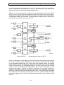
Figure LMP1-13 shows an overview of the internal structure of the ADC unit.
Figure LMP1-13
Structure of the ADC on the C167CR
The ADC works by comparing the input voltage to a fixed reference voltage between
VAGND (0 V) and VAREF (5 V). Voltages below and up to 0 V produce an output value of
0; voltages beyond 5 V produce the full scale value 0x3FF (all 10 bits set to ‘1’).
To configure the ADC for fixed channel single conversion operation the ADCON
register needs to be loaded with an appropriate value (cf. User Manual, p. 17-3).
Figure LMP1-14 shows the internal structure of the ADC control register ADCON.
13
Microcontroller Programming
Figure LMP1-14
LMP1: Introduction to µController programming
Structure of the ADCON register
The individual bits of ADCON determine the mode of operation (ADM), the channel to
be converted from (ADCH) and they allow a conversion to be started or stopped
(ADST). The busy flag (ADBSY) can be used to determine if a conversion is currently
ongoing (ADBSY == 1) or has been completed (ADBSY == 0). Alternative to polling the
ADBSY flag, a programmer can choose to trigger an interrupt once the conversion has
been completed. This can be done by assigning one of the 64 available interrupt levels
to the ADC. Special function register ADCIC is used to set this level (Figure LMP1-15).
Figure LMP1-15
Structure of the ADCIC register
A third way of noticing the end of a conversion is to poll the ADC interrupt request flag
(ADCIR). This flag is set upon completion of a conversion; it thus works inversely to
the ADBSY flag.
In our first ADC program we shall poll the ADCIR flag to detect the end of a
conversion. The triggering of the end-of-conversion interrupt will remain disabled
(ADCIE = 0). To configure the ADC for single conversions on channel 0 we have to set
the 2 bits of ADM to 00 (fixed channel, single conversion mode) and the 4 bits of
ADCH to 0000 (channel 0). All other bits can remain at their default value (0).
Altogether, ADCON will have to be loaded with 0x0000 (coincidentally this is the reset
value – strictly speaking, we wouldn’t have to assign a value to ADCON to configure
the ADC for single conversion on channel 0).
The next step is to start the conversion. This is done by setting bit 7 in ADCON. The
Keil compiler provides direct access to the ADST using the single-bit addressing mode
of the C167CR microcontroller. To start a conversion a programmer simply sets ADST
to ‘1’:
ADST = 1;
/* this starts a conversion (Keil)… */
Alternatively, ADCON could have been ORed with the following (positive) mask:
ADCON |= 0x0080;
/* alternative way of starting the ADC… */
14
Microcontroller Programming
LMP1: Introduction to µController programming
Enter the following program or copy’n’paste it from myUni:
MP → Course Material → Tutorials → C167CR → myADC.c
#include <stdio.h>
#include <reg167.h>
/* standard I/O header file (printf) */
/* special function registers of the C167 */
void main(void) {
unsigned int
myResult;
/* configure ADC for single conversion on channel 0 */
ADCON = 0;
/* start conversion */
ADST = 1;
/* wait for end of conversion */
while(ADCIR == 0) {}
/* fetch result from ADDAT */
myResult = ADDAT;
/* conversion finished -> print result */
printf("Converted value: %x\n", myResult);
/* endless loop to stop program from running into nowhere land */
while(1) {}
}
Compile the code and launch the debugger/simulator. From the Peripherals menu
open the ADC control window as well as the interrupt control window. In the ADC
control window set the input voltage of channel 0 to 2.5 V. In the interrupt control
window scroll down to find the ADC interrupt (ADCINT, cf. Figure LMP1-16).
Figure LMP1-16
ADC peripheral control window
15
Microcontroller Programming
LMP1: Introduction to µController programming
Step over the initialisation and the starting of the ADC (first two lines of code). Observe
that the ADC has been configured for single conversions on channel 0 and that the
conversion has been started (ADST == 1, ADBSY == 1).
Every A/D conversion takes a finite time (around 8 µs). The simulator is sufficiently
realistic to take these delays into account. When continuing to step through the code
you should notice that code execution is briefly held by
while(ADCIR == 0) {}
// wait for end of conversion
Keep an eye on the 3rd column of the interrupt control window (Interrupt requests) as
well as on the busy flag and the start/stop flag of the ADC (ADBSY and ADST,
respectively). As soon as the conversion is complete, the interrupt request flag ADCIR
is set and both busy and start/stop flag are reset (ADBSY = ADST = 0). The result of
the conversion can be found in ADDAT from where it can be fetched and displayed. As
2.5 V is exactly half of the full scale value (5 V), the result will be 0x3FF / 2 = 0x1FF
(top bit clear, remaining 9 bits set).
Continue to step through the code until you get to the printf line. When executing the
printf statement the simulator appears to hang. Why? (Figure LMP1-17)
Figure LMP1-17
Displaying the converted value – error?
Click on the red stop button (circle in Figure LMP1-17). This interrupts the currently
executing machine code. The simulator displays the disassembly of the code the
Instruction Program Counter (IPC) currently points to (here: address 0x1032A, see
Figure LMP1-18).
16
Microcontroller Programming
Figure LMP1-18
LMP1: Introduction to µController programming
Disassembly of the latest machine code instruction
Try to continue stepping through the code (step over). The controller appears to be
blocked by the highlighted line:
0001032A 9AB6FE70
JNB
S0TIR,0x01032A
This line of assembler code indicates that a flag S0TIR is tested and a jump to
0x1032A (i. e. back to this very line) is performed when S0TIR is zero. From the
Peripherals menu open the serial interface ASC0. Observe that the S0 Transmission
Interrupt Request flag is indeed cleared (Figure LMP1-19). No serial communication
appears to be happening.
Does this explain to you why the printf statement isn’t working? (It should… ☺
not, have a look at section 3 again)
– If
Stop debugging (red ‘d’-button) and fix your program. Re-compile everything and test
your modified program. The following output should appear on the serial terminal
window:
Converted value: 1ff
17
Microcontroller Programming
Figure LMP1-19
5.
LMP1: Introduction to µController programming
Confirming that flag S0TIR is cleared
A/D conversions with interrupts
In this section we are going to modify our ADC program to incorporate interrupts. The
objective is to understand how an interrupt can be triggered at the end of each
conversion. The converted value is to be displayed on a terminal connected to the
serial interface.
Polling the ADCIR flag or the ADBSY flag for the end of conversion seems pretty
wasteful as the controller is simply waiting for the ADC unit to complete its job. In most
situation this wasted time could (and should) be used to do other things, such as
perform a calculation, service a network connection or control external units via the
digital I/O lines. This is what interrupts are for.
Configured to trigger an end-of-conversion interrupt the ADC can run in the
background while the main program gets on with other things. Once a conversion is
complete the interrupt controller takes over and switches context from the main
program to an interrupt service routine (ISR). An ISR is a user supplied piece of code
which is executed when the associated interrupt is triggered.
Three things will have to be added to our program to make it work with interrupts:
(1)
(2)
(3)
An interrupt service routine (ISR) will have to be supplied
The ADC interrupt control register (ADCIC) needs to be configured to
define the priority level of the interrupt to be triggered.
All interrupts will have to be allowed to happen (processor flag)
18
Microcontroller Programming
LMP1: Introduction to µController programming
The C167CR implements a hierarchy of 16 main interrupt levels (ILVL). Each of these
levels is sub-divided into 4 sub-levels, the so-called group levels (GLVL). Altogether,
this gives a programmer the freedom of choosing up to 64 different priority levels
(higher order tasks can interrupt lower order tasks). In our case, however, we only
have a single interrupts source, namely the ADC. We can thus set the interrupt level
and/or group level to any value, say ILVL = 5, GLVL = 1.
Figure LMP1-15 (p. 14) shows the ADC interrupt control register (ADCIC). To
configure the ADC for the above values we need to set ILVL to 5 (= 0101) and GLVL to
1 (= 01). Furthermore, the ADC Interrupt Enable (ADCIE) needs to be set. In summary:
ADCIC = 0000.0000.0101.0101 = 0x0055;
ADCIE
GLVL
ILVL
The second modification of our program is the inclusion of an interrupt service routine
for the ADC interrupt. The online User Manual tells you that the ADC triggers an
interrupt with a reference number 0x28 (Chapter 5, Table 5-1). This interrupt reference
number denotes an entry within the interrupt vector table. It appears that the ADC
interrupt is the 0x28th (= 40th) entry in this table. The interrupt vector table is a list of 4byte starting addresses for all interrupt service routines know to the microcontroller.
The compiler needs to be instructed to place the starting address of our end-ofconversion ISR at vector number 0x28. This is done using the special attribute
‘interrupt’. A sub-routine can be defined as ISR using the following construct:
void myISR(void) interrupt <vector_number> {
…
}
In our case we would define the ISR ADC_finished as follows:
void ADC_finished(void) interrupt 0x28 {
/* ADC finished -> fetch result from ADDAT */
myResult = ADDAT;
}
Notice that the address of an interrupt vector can always be found by multiplying the
interrupt vector number by 4. This is because there are 4 bytes per interrupt vector.
For the end-of-conversion interrupt, the vector address is 4 * 0x28 = 0x00A0. This
value is displayed in the interrupt control window of the simulator/debugger.
Finally, in addition to supplying an interrupt service routine (ADC_finished) and
configuring the ADC interrupt control register (ADCIC) we also have to instruct the
microcontroller to allow all interrupts. The status register within the CPU of the
controller contains a general interrupt enable flag (IEN). This master switch can be
used to quickly enable/disable all configured interrupts. In our case this only affects the
ADC interrupt (as we haven’t allowed any other interrupts – yet).
Make the following modifications to the previous program or load the corresponding
electronic copy from myUni
MP → Course Material → Tutorials → C167CR → myADCint.c
19
Microcontroller Programming
#include <stdio.h>
#include <reg167.h>
LMP1: Introduction to µController programming
/* standard I/O header file (printf) */
/* special function registers of the C167 */
/* global variables */
unsigned int
myResult, oldResult;
/* end-of-conversion ISR */
void ADC_finished(void) interrupt 0x28 {
/* conversion complete -> fetch result from ADDAT */
myResult = ADDAT;
}
/* main program */
void main(void) {
/* initialize serial interface, 9600 bps, 8-N-1 */
DP3 |= 0x0400;
/* PORT 3.10 DIRECTION CONTROL: OUTPUT (TXD) */
DP3 &= ~0x0800;
/* PORT 3.11 DIRECTION CONTROL: INPUT (RXD) */
P3
|= 0x0400;
/* PORT 3.10 DATA: HIGH (LINE IDLE) */
S0TIC = 0x80;
/* SET TRANSMIT INTERRUPT FLAG (TX COMPLETE) */
S0RIC = 0x00;
/* CLEAR RECEIVE INTERRUPT FLAG (NOTHING REC.) */
S0BG = 0x40;
/* SET BAUDRATE TO 9600 BAUD */
S0CON = 0x8011;
/* SET SERIAL MODE */
/* initialize variables */
myResult = 0;
oldResult = 0;
/* configure ADC for single conversion on channel 0 */
ADCON = 0;
/* configure ADC interrupt control register */
ADCIC = 0x0055;
// ADCIE = 1, ILVL = 5, GLVL = 1
/* allow all interrupts */
IEN = 1;
/* start conversion */
ADST = 1;
while (1) {
/* only plot result if something's changed */
if(myResult != oldResult) {
/* new value -> print result */
printf("Converted value: %x\n", myResult);
oldResult = myResult;
}
}
}
Comments:
The program starts by initialising the serial interface (we’re using printf to display the
result of our conversion) before initialising two global variables (myResult and
oldResult). Notice that at least the variable myResult needs to be global as we are
accessing it from within the main program as well as the ADC interrupt service routine.
The program continues by configuring the ADC (ADCON, ADCIC) before the interrupts
are allowed to happen (IEN = 1). Following the starting of the conversion (ADST = 1)
we enter an infinite loop in which new results are displayed on a terminal connected to
the serial interface.
Compile this program and load it into the simulator/debugger. Open the peripheral
windows for ADC as well as the interrupt control window. Step through the code and
observe how the interrupt levels and group levels are programmed as expected (Figure
LMP1-20).
20
Microcontroller Programming
Figure LMP1-20
LMP1: Introduction to µController programming
End-of-conversion interrupts
Set the value of channel 0 to 2.5 V and continue to step through the code. Execution is
briefly blocked at the line
while(myResult != oldResult) { … }
Notice that we’ve initialised both of these variables to zero, i. e. nothing will be
displayed unless a conversion has taken place. When the ongoing conversion is
complete (after a few clicks) the interrupt request flag (ADCIR) is set and the end-ofconversion interrupt is triggered. The main program is interrupted and code execution
resumes inside the interrupt service routine ADC_finished. Notice that upon entry to
the ISR, the interrupt controller automatically resets the interrupt request flag (ADCIR).
This is a particularity of the C167CR. Other microcontroller might require the
programmer to ensure that the interrupt request flag is cleared.
The ISR loads the global variable myResult with the conversion result found in ADDAT
before returning to the main program. This, in turn, breaks the blockage of the main
program (myResult != oldResult) which resumes operation by printing the result of the
conversion.
Continue to step through the program. You should observe that following the first
successful conversion, the program doesn’t seem to do a great deal… it seems that
we’re stuck on the above while line, even if we change the voltage of channel 0 to
another value (e.g. 1 V). The reason, of course, is that we have configured the ADC for
single conversions. Change the voltage to 1 V and check the box next to ADST. This
has the effect of re-starting the ADC. After a few clicks of the mouse, the conversion is
complete and the interrupt is triggered again (converted value: cc).
21
Microcontroller Programming
LMP1: Introduction to µController programming
Now try to change the operational mode from single conversion to continuous
conversion. You can do this by selecting Single Channel Continuous Conversion from
the list box of the ADC control window. Enter a new voltage for channel 0 (e.g. 2 V)
and start the ADC (check box next to ADST). Notice that the value of ADCON has
changed to 0x0190.
Continue to step through the code. You should observe that interrupt is triggered very
frequently now. In fact, we almost immediately re-enter the ISR as soon as we get out.
Try a few voltages to ensure that your program is working correctly (Figure LMP1-21).
Figure LMP1-21
ADC in continuous conversion mode
Notice that you could have chosen to re-scale the converted result to a range from 0 to
5 V using
myResult_scaled = (float)myResult / 0x3FF * 5;
where myResult_scaled is a variable of type float.
6.
Timer
All digital signal processing and control applications require tasks to be run in real time.
The term “real time” refers to the requirement of synchrony between external real world
events and events triggered by the microcontroller (e.g. the acquisition of an analogue
value through the ADC or the output of a controller response through a digital I/O line
or a D/A converter).
22
Microcontroller Programming
LMP1: Introduction to µController programming
A microcontroller can be programmed to run at a particular sample rate using timers
and the associated interrupt service routines. In this section you will learn how to
generate a pulse train with a fixed programmable period.
Chapter 10 of the User Manual introduces the general purpose timer units (GPT1,
GPT2) of the C167CR. Most microcontrollers have similar timing units. Figure LMP122 shows a block diagram of the general purpose timer unit GPT1. This unit comprises
3 independent timers, the core timer T3 as well as two auxiliary timers T2 and T4. In
this exercise we will program the core timer T3.
Figure LMP1-22
General purpose timer unit GPT1
A timer is essentially a 16-bit register whose value can be incremented or decremented
by internal or external events. External events are commonly rising and/or falling edges
on an associated digital input line. When used with external events, the general
purpose timer is said to be operating in (gated) counter mode, as it is simply counting
events. Internal events are rising/falling edges of the CPU clock signal and overflow
events of other timer registers (cascaded timers). As the CPU clock signal is a very
regular timing pattern, counting its edges is equivalent to measuring durations or
periods of time (timer mode). The maximum period of a timer depends on the clock
frequency as well as the programmed initial timer value. The latter denotes a threshold
from which the timer counts up towards 0xFFFF or down towards 0x0000. Reaching
these limits triggers a timer overflow (underflow) interrupt which can be used to restart
the timer.
23
Microcontroller Programming
LMP1: Introduction to µController programming
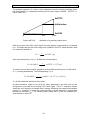
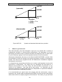
The principal operation of a timer is best explained using the following diagram which
has been drawn for a downward counting 16-bit timer (range: 0x0000 – 0xFFFF, cf.
Figure LMP1-23):
0xFFFF
Initial value
0
0x0000
duration
Figure LMP1-23
Tinit
Tmax
Operation of a general purpose timer
With every cycle of the CPU clock signal, the timer register is decreased (or increased)
by 1. Counting through the entire range from 0x0000 to 0xFFFF would therefore lead
to a maximum duration of
Tmax =
1
f CPU
⋅ 0 xFFFF [s].
With a clock frequency of fCPU = 20 MHz this corresponds to
Tmax (20 MHz ) =
1
⋅ 0 xFFFF = 3.277 [ms ] .
20 ⋅ 10 6
The minimum time that could be programmed at 20 MHz would require an initial value
of ‘1’ (counting downwards). The corresponding Tmin is
Tmin (20 MHz ) =
1
⋅ 0 x0001 = 5.0 ⋅ 10 −8 [ s ] = 50 [ns ] .
6
20 ⋅ 10
Tmin is also called the resolution of the timer.
As these durations might be too small for many applications, the timer unit can be
configured to pre-scale the incoming CPU clock signal. This 2n:1 frequency divider
allows the clock signal to be slowed down, thereby increasing the maximum accessible
period Tmax. However, it should be noted that this is at the expense of a decreased
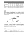
resolution (increased Tmin). The following table (Table LMP1-1) lists the available prescale factors for timer T3:
24
Microcontroller Programming
LMP1: Introduction to µController programming
Table LMP1-1 Timer T3 – Pre-scale factors
Example:
With a pre-scale factor of 512 the effective timer frequency is 20 MHz / 512 = 39.06
kHz. This corresponds to a per-step increment of ∆t = 1/(39.06·103) = 25.6 µs.
Counting up all 16-bit (0x0000 – 0xFFFF) yields a maximum period of 25.6 µs x
0xFFFF = 1.68 s. To program a period of 1 second we would have to initialise the timer
register with 1/1.68 x 0xFFFF = 0x9860 and count downwards. Figure LMP1-24
illustrates this example.
0xFFFF
0x9860
0s
0x0000
1.68 s
1s
Figure LMP1-24
Programming a 1 second timer period (T3)
To configure timer T3 for this sort of operation we would have to initialise the T3
control register (T3CON) with a pre-scale factor of 512. Figure LMP1-25 shows the
internal structure of the timer T3 control register. As indicated by table LMP1-1, the
timer input selection bits (T3I) need to be set to 110.
Figure LMP1-25
Timer T3 control register
25
Microcontroller Programming
LMP1: Introduction to µController programming
The function of the remaining bits can be found from the User Manual (p. 10-3). T3M
denotes the mode of operation (timer, counter, gated counter, etc.), T3R starts and
stops the timer, T3UD (up/down) indicates whether the timer is incrementing or
decrementing, etc.
Interesting effects can be achieved in conjunction with the alternate output function pin
T3OUT (internally connected to port P3.3). Enabling the alternate output function
(T3OE = 1) allows the state of the output toggle flag T3OTL to be displayed on P3.3.
This port pin will have to be set-up as output (DP3.3 = 1) and initialised with a logical
high level (P3.3 = 1). Flag T3OTL is toggled every time the timer overflows (when
counting up) or underflows (when counting down). Programming a periodic timer with a
period of say 1 second would therefore produce an output pulse train on P3.3 with a
period of 2 seconds (1 second ON, 1 second OFF). Figure LMP1-26 illustrates the use
of the alternate output function pin T3OUT.
Figure LMP1-26
Alternate output function of timer T3
It should be noted that timer T3 can be made periodic using an automatic reload
mechanism. The auxiliary timer registers T2 and T4 can be configured as reload
registers with every T3 overflow (underflow) triggering an automatic transfer of the
contents of T2 (or T4) into timer register T3. This reload operation is activated through
the respective timer control registers T2CON or T4CON, respectively. Details can be
found in the User Manual (p. 10-17 f.). Figure LMP1-27 shows the internal structure of
T2CON, Figure LMP1-28 illustrates the automatic reload mechanism.
Figure LMP1-27
Timer T2 control register T2CON
26
Microcontroller Programming
Figure LMP1-28
LMP1: Introduction to µController programming
Block diagram of the auxiliary timer T2 (T4) in reload mode
Programming a timer is pretty similar to programming an A/D converter. A number of
special function registers have to be configured, an interrupt priority level might have to
be selected, etc. In summary, the following aspects need to be looked at:
The timer unit first needs to be configured for timer mode with a particular pre-scale
factor (T3CON). An initial timer value will have to be placed in the timer register T3. To
activate the automatic reloading mechanism the auxiliary timer register T2 (or T4) will
have to be loaded with the same value; the corresponding timer control register
(T2CON, T4CON) needs to be configured for reload operation.
If the timer is meant to trigger interrupts, an interrupt priority level needs to be set in
T3IC (structurally identical to ADCIC). Furthermore, an interrupt service routine needs
to be provided for T3INT (vector 0x23) and all interrupts need to be enabled in general
(IEN = 1).
If the alternate output function (T3OUT) is to be used, we also need to program port
P3.3 as output and initialise it with a logic high level.
The following program generates a regular square wave signal with a period of 2
seconds and a duty cycle of 50% (1 second ON, 1 second OFF). Enter this program or
simply copy it from myUni:
MP → Course Material → Tutorials → C167CR → myT3.c
#include <reg167.h>
/* special function registers of the C167 */
/* main program */
void main(void) {
/* configure T3 for timer mode, pre-scale factor 512, period: 1 second */
/* enable alternate output function T3OUT, load toggle bit T3OTL with '0' */
/* T3CON = 0000.0010.1000.0110 = 0x0286 */
T3CON = 0x0286;
/* program port 3, pin 3 as output, initialise with '1' */
27
Microcontroller Programming
DP3 |= 0x0008;
P3 |= 0x0008;
LMP1: Introduction to µController programming
// pin 3
// pin 3
/* load initial timer value T3 */
T3 = 0x9860;
// this represent a duration of 1 second (pre-scale factor 512)
/* load auxilary timer T2 with the same value (reload value) */
T2 = 0x9860;
/* configure auxilary timer for reload mode, any transition of T3OTL */
/* T2CON = 0000.0000.0010.0111 = 0x0027 */
T2CON = 0x0027;
// reload mode
/* start timer */
T3R = 1;
/* keep program from running into cyberspace */
while (1) { }
}
Upon compilation, launch the simulator/debugger and display the peripheral control
windows for timer T3, auxiliary timer T2 as well as for the parallel port P3. Step through
the code carefully observing how the timer registers and flags are affected by the
commands (Figure LMP1-29).
Figure LMP1-29
Simulating a periodic timer
It quickly becomes apparent that single stepping is not very efficient when trying to
understand timers: It takes around 60 – 70 clicks of the mouse to decrease the timer
register by one… (don’t do this – use F10 instead, please ).
To by-pass this problem we can define a conditional breakpoint. From the Debug
menu, select ‘Breakpoints…’. You should be presented with a window allowing you to
define and edit complex breakpoints.
28
Microcontroller Programming
LMP1: Introduction to µController programming
Click inside the text box Expressions and enter the following condition:
T3 == 0
Click on Define and Close the window. This instructs the simulator to halt execution
when timer register T3 reaches 0. From the View menu select Periodic Window
Update, then start execution by clicking on the RUN button (see small circle in Figure
LMP1-29).
Observe how the timer register T3 is decremented until the value 0 is reached. On a
real C167CR microcontroller running at 20 MHz this would take exactly 1 second. The
execution speed of the simulation, on the other hand, depends on the features of the
underlying computer hardware (processor, memory, etc.).
Once T3 is zero we regain control. Single-step through the code until T3 is
decremented to 0xFFFF (underflow). This should take approximately 60 odd steps
(use F10). Observe that the output toggle flag T3OTL has been set. This flag is also
displayed on T3OUT (= P3.3). On a real microcontroller we would be able to measure
a logical high level (5 V) on the associated pin. Also note that the timer register T3 has
been reloaded with the value from T2 (0x9860) and that the timer T3 interrupt request
flag (T3IR) has been set. This could be used to divert execution control from the main
program to an interrupt service routine (T3INT).
You can click on RUN again to repeat this experiment. Stop the debugger/simulator
when you get bored…
Conclusion:
It should be noted that other microcontrollers might implement their timer/counter
control in a slightly different way. However, the fundamental concept is always the
same: A pre-scale factor is chosen to slow down the otherwise too fast running clock
signal; for a 16-bit timer/counter this selects a maximum timer period of
Tmax = (pre-scale factor)/fOSC x 0xFFFF
(Example: Tmax = 512 / (20·106) x 0xFFFF = 512 / (20·106) x 65535 = 1.678 seconds). A
fine adjustment within this maximum period can be achieved with the initial value /
reload value of the timer. Initialising the timer (and/or the reload register) with a smaller
value than 0xFFFF reduces the maximum period to a smaller value. Depending on the
direction of the timer (counting upwards or downwards) two scenarios are possible
(Figure LMP1-30).
Once a suitable period has been programmed and the timer has been configured for
single-shot operation or reload operation, execution can be started (timer run).
Interrupts can be configured to be triggered by timer overflows and/or underflows or
upon reaching the threshold value (reload value). With an appropriate interrupt service
routine a timer can be used to toggle output pins in a regular timely manner (frequency
generation, pulse width modulation, etc.). Other uses of timers include the periodic
computation of system equations (digital control, filters) and the periodic servicing of
ADCs and DACs.
29
Microcontroller Programming
LMP1: Introduction to µController programming
0xFFFF
(upwards)
0x9860
0x0000
1.68 s
0s
1s
Duration
= 1.68 s – 1 s
= 0.68 s
0xFFFF
(downwards)
0x9860
0s
Duration
=1s
Figure LMP1-30
7.
1s
0x0000
1.68 s
Upward and downward directed timer operation
Where to go from here?
This initial laboratory has been designed to get you up to speed with a number of
fundamental concepts of microcontroller programming. The advantage of the Keil
developing environment with its powerful simulator will hopefully make it a little easier
for you to develop a grasp of the most important elements of a microcontroller.
Subsequent laboratories will focus on the Motorola MC9S12DP256B, a similar 16-bit
microcontroller of which the School has recently purchased a number of development
boards. The 9S12 will be programmed with the Metrowerks CodeWarrior integrated
development environment.
It is hoped that this introduction will allow you to make a swift transition from the Keil
environment to Metrowerks. The reason why we developed this lab based on a
different microcontroller is two fold. Firstly, the Keil simulation environment is very
intuitive (if you disagree – wait until you’ve seen others… ☺). Secondly, you are
expected to develop conceptual skills which are independent of a particular hardware.
All microcontrollers are essentially the same…
It is recommended you spend some time playing with this environment, trying to
implement, say, a pulse width modulated signal (PWM). Consult the online help system
and/or have a look for sample programs on the Internet. The earlier you get your head
30
Microcontroller Programming
LMP1: Introduction to µController programming
around the introduced concepts, the more likely it is you will benefit from the remaining
laboratory sessions.
Take this series of laboratories as a preview of what to expect in the work environment
of a mechatronics engineer. You will almost certainly have to be able to find relevant
information from data sheets or some manufacturer’s instruction manuals and you’ll
have to be able to learn about new techniques you may not yet be familiar with (e.g. a
new programming language, a piece of equipment you’ve never before come across,
etc.).
The good news… ? You won’t be sacked if you don’t mange to do it all within 6 weeks.
☺
31