1
CT-DBT0x
3.5” Industrial Single Board Computer
with Intel® Atom™ Processor E3800
User’s Manual
Version 100 Preliminary
April 13, 2015
C&T Solution Inc.
17F-2, No. 700, Zhongzheng Rd., Zhonghe Dist., New Taipei City 235, Taiwan
Tel: +886-2-7731-7888
CT-DBT0x 3.5’’ SBC
http://www.candtsolution.com
Preface
Revision History
Rev.
Date
Description
100
13/04/2015
Initial release
Disclaimer
All specifications and information in this User’s Manual are believed to be
accurate and up to date. C&T Solution Inc. does not guarantee that the
contents herein are complete, true, accurate or non-misleading. The
information in this document is subject to change without notice and does not
represent a commitment on the part of C&T Solution Inc.
C&T Solution Inc. disclaims all warranties, express or implied, including,
without limitation, those of merchantability, fitness for a particular purpose with
respect to contents of this User’s Manual. Users must take full responsibility for
the application of the product.
Copyright Notice
All rights reserved. No part of this manual may be reproduced or transmitted in
any form or by any means, electronic or mechanical, including photocopying,
recording, or information storage and retrieval systems, without the prior
written permission of C&T Solutions Inc.
Copyright © 2015 C&T Solutions Inc.
2
CT-DBT0x 3.5’’ SBC
Trademarks Acknowledgment
Intel®, Celeron® and Pentium® are trademarks of Intel Corporation.
Windows® is registered trademark of Microsoft Corporation.
AMI is trademark of American Megatrend Inc.
IBM, XT, AT, PS/2 and Personal System/2 are trademarks of International
Business Machines Corporation
All other products and trademarks mentioned in this manual are trademarks of
their respective owners.
Environmental Protection Announcement
Do not dispose this electronic device into the trash while discarding. Please
recycle to minimize pollution and ensure environment protection.
3
CT-DBT0x 3.5’’ SBC
Safety Precautions
Before installing and using the equipment, please read the following
precautions:
z Put this equipment on a reliable surface during installation. Dropping it or
letting it fall could cause damage.
z The power outlet shall be installed near the equipment and shall be easily
accessible.
z Turn off the system power and disconnect the power cord from its source
before making any installation. Be sure both the system and the external
devices are turned OFF. Sudden surge of power could ruin sensitive
components. Make sure the equipment is properly grounded.
z When the power is connected, never open the equipment. The equipment
should be opened only by qualified service personnel.
z Make sure the voltage of the power source is correct before connecting the
equipment to the power outlet.
z Disconnect this equipment from the power before cleaning. Use a damp
cloth. Do not use liquid or spray detergents for cleaning.
z Avoid the dusty, humidity and temperature extremes.
z Do not place heavy objects on the equipment.
z If the equipment is not used for long time, disconnect it from the power to
avoid being damaged by transient over-voltage.
z The storage temperature shall be above -20°C and below 80°C.
z The computer is provided with a battery-powered real-time clock circuit.
There is a danger of explosion if incorrectly replaced. Replace only with
the same or equivalent type recommended by the manufacturer.
z If one of the following situation arises, get the equipment checked be
service personnel:
The power cord or plug is damaged.
Liquid has penetrated into the equipment.
The equipment has been exposed to moisture.
The equipment does not work well or it cannot work according the
user’s manual.
The equipment has been dropped and damaged.
The equipment has obvious signs of breakage.
4
CT-DBT0x 3.5’’ SBC
Table of Contents
Preface............................................................................................................2
1.
Introduction.............................................................................................8
1.1
Product Description ..............................................................................8
1.2
Specifications .......................................................................................9
1.3
Available Models ................................................................................12
1.4
Block Diagram ....................................................................................13
2.
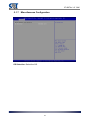
Mechanical Specifications ...................................................................14
2.
Mechanical Specifications ...................................................................14
2.1
Dimensions.........................................................................................14
2.2
Board Layout ......................................................................................15
2.2.1
2.3
Connectors & Jumpers ......................................................................... 15
External Connectors ...........................................................................16
2.3.1
Serial Port COM1.................................................................................. 16
2.3.2
VGA Connector..................................................................................... 17
2.3.3
USB 3.0 Connector ............................................................................... 18
2.3.4
USB 2.0 Connectors ............................................................................. 18
2.3.5
HDMI Connector ................................................................................... 18
2.3.6
LAN Connector ..................................................................................... 18
2.4
Internal Connectors ............................................................................19
2.4.1
Front Panel Audio Connector (AUDIO)................................................. 19
2.4.2
Backlight Control Connector (CN1) ...................................................... 19
2.4.3
COM2-4 Serial Ports (COM2-4)............................................................ 19
2.4.4
LPC Connector (DBG) .......................................................................... 20
2.4.5
Fan Connector (FAN)............................................................................ 20
2.4.6
GPIO Connector: GPIO ........................................................................ 20
2.4.7
Power Button Pin Header (JP3)............................................................ 20
2.4.8
Reset Button Pin Header (JP4) ............................................................ 21
2.4.9
Reset Button Pin Header (JP6) ............................................................ 21
2.4.10
I2C Pin Header (I2C1) .......................................................................... 21
2.4.11
Multi-LED Pin Header (LED)................................................................. 21
2.4.12
LVDS Connector: LVDS ....................................................................... 22
2.4.13
microSD Connector (MICRO_SD) ........................................................ 22
2.4.14
Mini-PCIe Slot #1 (PCIE1_MSATA)...................................................... 23
2.4.15
Mini-PCIe Slot #2 (MINI_PCIE1) .......................................................... 24
5
CT-DBT0x 3.5’’ SBC
2.4.16
ATX Power Connector (POWER_CONN) ............................................ 24
2.4.17
PS/2 Keyboard/Mouse Connector (PS2) .............................................. 24
2.4.18
SATA Signal Connectors: SATA1-2 ..................................................... 25
2.4.19
SATA Power Connectors (SATA1/2_PWR).......................................... 25
2.4.20
USB 2.0 Pin Header (USB_1/2)............................................................ 25
2.5
3.
Jumper Settings..................................................................................26
2.5.1
Backlight Power (JP1)........................................................................... 26
2.5.2
Panel Power (JP2) ................................................................................ 26
2.5.3
Clear CMOS (JP8) ................................................................................ 26
Features & Interfaces ...........................................................................27
3.1
Processor ...........................................................................................27
3.2
BIOS ...................................................................................................27
3.3
System Memory..................................................................................27
3.4
Graphics .............................................................................................27
3.5
USB ....................................................................................................28
3.6
Ethernet ..............................................................................................28
3.7
SATA ..................................................................................................28
3.8
Audio ..................................................................................................28
3.9
Expansion...........................................................................................28
3.10
General Purpose Input Output............................................................29
3.10.1
3.11
GPIO Configuration............................................................................... 29
Watchdog Timer .................................................................................31
3.11.1
Board Design ........................................................................................ 31
3.11.2
Psuedo Code ........................................................................................ 31
4.
Driver Installation .................................................................................32
5.
System BIOS .........................................................................................33
5.1
Advanced............................................................................................34
5.1.1
ACPI Settings........................................................................................ 35
5.1.2
F81866 Super IO Configuration............................................................ 36
5.1.3
Hardware Monitor ................................................................................. 37
5.1.4
Serial Port Console Redirection............................................................ 38
5.1.5
CPU Configuration ................................................................................ 39
5.1.6
SATA Configuration .............................................................................. 40
5.1.7
Miscellaneous Configuration................................................................. 41
5.1.8
LPSS & SCC Configuration .................................................................. 42
5.1.9
Network Stack Configuration ................................................................ 43
5.1.10
CSM Configuration................................................................................ 43
6
CT-DBT0x 3.5’’ SBC
5.1.11
SDIO Configuration............................................................................... 44
5.1.12
USB Configuration ................................................................................ 45
5.1.13
Security Configuration........................................................................... 46
5.2
Chipset ...............................................................................................47
5.2.1
Northbridge Configuration..................................................................... 47
5.2.2
Southbridge Configuration .................................................................... 50
5.3
Security...............................................................................................52
5.3.1
6.
Secure Boot Menu ................................................................................ 53
5.4
Boot ....................................................................................................54
5.5
Save and Exit .....................................................................................55
Address Map .........................................................................................56
6.1
I/O Port Address Map .........................................................................56
6.2
Interrupt Controller (IRQ) Map ............................................................59
6.3
Memory Map.......................................................................................67
7
CT-DBT0x 3.5’’ SBC
1. Introduction
1.1
Product Description
The CT-DBT0x is a single board computer in 3.5” SBC form factor featuring
the Intel® Atom™ Processor E3800 Series in FCBGA1170 package on 22nm
process technology in a single chip solution. One 240-pin SODIMM sockets
supports non-ECC/unbuffered DDR3L 1333MHz memory up to 4GB. The
Intel® HD graphics controller integrated within the processor supports three
independent displays (VGA, HDMI, LVDS). The CT-DBT0x supports
2x Gigabit Ethernet, USB 3.0/2.0, COM, GPIO, 2x Mini-PCIe slots, microSD
card SIM card to support a variety of industrial applications.
8
CT-DBT0x 3.5’’ SBC
1.2
Specifications
CPU
Intel® Atom™ Processor E3800 Series and Intel® Celeron®
Processor J1900 SoC in FCBGA1170 package
¾ Atom™ E3845: 4-core, 1.91GHz, TDP 10W
¾ Atom™ E3827: 2-core, 1.75GHz. TDP 8W
¾ Atom™ E3815: 1-core, 1.46GHz, TDP 5W
¾ Celeron® J1900: 4-core, 2.00GHz, TDP 10W
¾ Celeron® N2807: 4-cores, 1.58GHz, TDP 4.3W
System Memory
¾ One 204-pin DDR3L SODIMM socket
¾ 1333MHz, non-ECC unbuffered
¾ Data transfer rates up to 1333MT/s
¾ Up to 4GB
BIOS
¾ AMI uEFI BIOS
¾ 8MB SPI flash ROM
Graphics
¾ Intel® HD Graphics Gen 7 integrated in CPU
¾
¾
1x VGA, resolution up to 2560x1600@60Hz
1x HDMI 1.4a interface, up to 1920x1080@60Hz
Ethernet
¾ Two Intel® I210IT GbE Controllers
¾ 10/100/1000BASE-TX Ethernet
¾ WOL/PXE support
Audio
¾ Realtek ALC886
¾ Line-In, Line-Out and Mic-In
9
CT-DBT0x 3.5’’ SBC
Internal I/O
¾ 2x 7-pin SATA 3Gb/s ports (w/ 2x +12V/+5V/GND power)
¾ 4x USB 2.0 ports via header (1 from SoC, 3 from
USB 2.0 Hub IC, Genesys GL852GT-OHY12)
¾ 1x RS-232/422/485 port (BIOS selectable, supports
auto-flow)
¾ 3x RS-232 ports via header (COM2-4)
¾ 1x 8-bit GPIO (4-bit input, 4-bit output, +5V level,
GPO default “High”, GPI supports SMI trigger)
¾ 1x PS/2 keyboard and mouse
¾ 1x front panel audio
¾ 1x Reset button header
¾ 1x Power on/off header
¾ 1x wafer connector for external CMOS battery (included)
¾ 1x header for I2C Serial IO interface from SoC
¾ 1x Clear CMOS header
¾ 1x 4-pin fan connector
¾ 1x 4-pin ATX power connector for +12VDC power input
External I/O
¾ +12V DC power input
¾ 1x HDMI port (vertical)
¾ 1x VGA (DB-15)
¾
¾
¾
¾
2x GbE (RJ-45)
1x USB 3.0
1x USB 2.0
1x RS-232/422/485 COM1 (DB-9,
RS-485 auto low control supported)
Expansion
¾ 2x Mini PCIe slots, full size
Mini PCIe slot #1: PCIe x1 only or mSATA only
(by BOM option, see 1.3 Available Models)
Mini PCIe slot #2: PCIe x1 & USB 2.0
(USB 2.0 port from USB Hub IC)
¾ 1x microSD card slot
¾ 1x SIM card slot
Watchdog Timer
¾ H/W Reset, 1-255 sec./min.
¾ 1 sec. or 1min. increments
10
CT-DBT0x 3.5’’ SBC
Hardware Monitor
¾ System voltages
z CPU core power
z CPU I/O power
z DDR power
z VCC3
z Vin
¾ Temperatures monitoring
¾ Smart Fan support
Power
¾ DC +12V input
¾ ACPI 5.0 compliant
Form Factor
¾ 3.5” SBC, 146mm x 102mm
Operating Temp.
¾ -20°C to 70°C
Storage Temp.
¾ -40°C to 85°C
Operating Humidity
¾ 10% to 90% relative humidity, non-condensing
Certifications
¾ CE
¾
FCC Class A
11
CT-DBT0x 3.5’’ SBC
1.3
Available Models
Model
CT-DBT01
CT-DBT02
Processor
Ordering Information
Part Number
Atom™ E3845
CT-DBT01-E3845
6-DBT0101S100-P0
Atom™ E3827
CT-DBT01-E3827
6-DBT0102S100-P0
Atom™ E3815
CT-DBT01-E3815
6-DBT0103S100-P0
Celeron® J1900
CT-DBT01-J1900
6-DBT0104S100-P0
Celeron® N2807
CT-DBT01-N2807
6-DBT0105S100-P0
Atom™ E3845
CT-DBT02-E3845
6-DBT0201S100-P0
Atom™ E3827
CT-DBT02-E3827
6-DBT0202S100-P0
Atom™ E3815
CT-DBT02-E3815
6-DBT0203S100-P0
Celeron® J1900
CT-DBT02-J1900
6-DBT0204S100-P0
Celeron® N2807
CT-DBT02-N2807
6-DBT0205S100-P0
Mini PCIe Slot BOM Options
Mini PCIe slot #1
Mini PCIe slot #2
CT-DBT01
PCIe x1 only
PCIe x1 & USB 2.0
CT-DBT02
mSATA only
PCIe x1 & USB 2.0
12
CT-DBT0x 3.5’’ SBC
1.4
Block Diagram
DDR3
1066/1333MHz
DDR3/L
240-pin SODIMM
Channel 0
VGA
DDI0
HDMI
DDI1
Intel®
Atom™
E3800
I2C
BIOS
SATA x2
USB 3.0 x1
USB 2.0 x2
SPI
2x SATA
Celeron®
J1900/N2807
SoC
LVDS
SDMMC
PCIe x1,
Port 0
PCIe x1,
Port 1
microSD
I210IT
RJ-45
I210IT
RJ-45
LPC
USB 3.0
GPI x4
GPO x4
F81866AD-I
USB 2.0
COM1-4
1x USB 2.0 port
2x USB header
Mini PCIe
Slot #2
Mini PCIe
Slot #1
USB 2.0
USB Hub
PS/2 KB/MS
PCIe x1
Fan
PCIe x1 or mSATA
HD
Audio
ALC886
Line-Out
13
Mic-In
CT-DBT0x 3.5’’ SBC
2. Mechanical Specifications
2.1
Dimensions
Units: mm
14
CT-DBT0x 3.5’’ SBC
2.2
Board Layout
2.2.1
Connectors & Jumpers
Connector
Description
Connector
Description
AUDIO
CN1
COM1
COM2-4
DBG
DIMM
FAN
GPIO
HDMI
JP1
JP2
JP3
JP4
JP6
JP8
Front Audio connector
Backlight Control connector
RS-232/422/485 DB9 connector
RS-232 COM2-4 headers
LPC connector
240-pin SODIMM socket
Fan connector
GPIO header
HDMI port
Backlight Power Select jumper
Panel Power Select jumper
Power Button header
Reset Button header
Battery connector
Clear CMOS
I2C1
LED
LVDS
MICRO_SD
MINI_PCIE2
PCIE1_MSATA
POWER_CONN
PS2
RJ45
SATA1/2
SATA1/2_PWR
SIM1
USB_1/2
USB_3
VGA
I2C header
LED header
LVDS connector
microSD card slot
Mini PCI Express slot 2
Mini PCI Express slot 1
ATX Power connector
PS/2 KB/MS wafer connector
LAN ports
SATA Port 1/2 signal connector
SATA Port 1/2 power connector
SIM card slot
USB 2.0 headers
USB 2/0/3.0 ports
VGA connector
15
CT-DBT0x 3.5’’ SBC
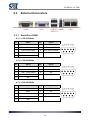
2.3
External Connectors
COM1
2.3.1
VGA
USB 2.0 HDMI
USB 3.0
Serial Port COM1
2.3.1.1 RS-232 Mode
Pin
Signal
Pin
Signal
1
DCD, Data Carrier Detect
6
DSR, Data Set Ready
2
RXD, Receive Data
7
RTS, Ready To Send
3
TXD, Transmit Data
8
CTS, Clear To Send
4
DTR, Data Terminal Ready
9
RI, Ring Indicator
5
GND, Ground
2.3.1.2 RS-422 Mode
Pin
Signal
Pin
Signal
1
TXD-, Transmit Data
6
NA
2
RXD+, Receive Data
7
NA
3
TXD+, Transmit Data
8
NA
4
RXD-, Receive Data
9
NA
5
NA
2.3.1.3 RS-485 Mode
Pin
Signal
Pin
Signal
1
Data-
6
NA
2
Data+
7
NA
3
NA
8
NA
4
NA
9
NA
5
NA
16
LAN
CT-DBT0x 3.5’’ SBC
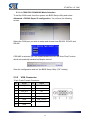
2.3.1.4 COM1 RS-232/422/485 Mode Selection
To set the COM mode, boot the system into BIOS Setup Utility and select
Advanced > F81866 Super IO configuration. You will see the following
screen.
Select the COM port you wish to setup and choose from RS-232, RS-422 and
RS-485.
If RS-485 is selected, you can enable/disable the RS-485 Auto Flow Function
which automatically handles half-duplex control.
Save the configuration and exit the BIOS Setup Utility ("F4" hotkey).
2.3.2
VGA Connector
15-pin D-sub Female Connector
Pin
Signal
Pin
Signal
1
VGA_RED
9
VCC
2
VGA_GRN
10
GND
3
VGA_BLU
11
NC
4
NC
12
VGA_DDC_DAT
5
GND
13
VGA_HSYNC
6
GND
14
VGA_VSYNC
7
GND
15
VGA_DCC_CLK
8
GND
17
CT-DBT0x 3.5’’ SBC
2.3.3
USB 3.0 Connector
2.3.4
Pin
Signal
Pin
Signal
1
USB +5V
5
USB_SSRX-
2
USB_D-
6
USB_SSRX+
3
USB_D+
7
GND_DRAIN
4
GND
8
USB_SSTX-
9
USB_SSTX+
USB 2.0 Connectors
2.3.5
Pin
Signal
1
USB +5V
2
USB_D-
3
USB_D+
4
GND
1
2
3
4
HDMI Connector
Pin
Signal
Pin
Signal
1
HDMI_TX2_DP_B
2
GND
3
HDMI_TX2_DN_B
4
HDMI_TX1_DP_B
5
GND
6
HDMI_TX1_DN_B
7
HDMI_TX0_DP_B
8
GND
9
HDMI_TX0_DN_B
10
HDMI_CLK_DP_B
11
GND
12
HDMI_CLK_DN_B
13
NC
14
NC
15
HDMI_SCLDDC_B
16
HDMI_SDADDC_B
17
GND
18
+5V
2.3.6
LAN Connector
Pin
Signal
Pin
Signal
1
MDI0+
5
MDI2-
2
MDI0-
6
MDI1-
3
MDI1+
7
MDI3+
4
MDI2+
8
MDI3-
A
Active LED
B
10 LAN LED (OFF)
(Yellow)
100 LAN LED (Green)
1000 LAN LED (Orange)
18
19
1
18
2
CT-DBT0x 3.5’’ SBC
2.4
Internal Connectors
2.4.1
Front Panel Audio Connector (AUDIO)
Connector Type: 2x6-pin pitch 2.00mm wafer connector
Pin
Signal
Pin
Signal
1
MICIN_L
2
MICIN_R
3
MIC1_JD
4
AGND
5
LOUT_L
6
LOUT_R
7
FRONT_JD
8
AGND
9
LIN_L
10
LIN_R
11
LINE1_JD
12
AGND
2.4.2
1
3
5
7
9
11
2
4
6
8
10
12
Backlight Control Connector (CN1)
Connector Type: 1x8-pin pitch 2.0mm wafer connector
Pin
Signal
Pin
Signal
1
Backlight Enable
2
Backlight CTRL
3
Backlight PWR
4
Backlight PWR
5
GND
6
GND
7
Brightness UP
8
Brightness DOWN
2.4.3
COM2-4 Serial Ports (COM2-4)
Connector Type: 1-9-pin pitch 2.0mm wafer connector
Pin
Signal
Pin
Signal
1
DCD, Data Carrier Detect
2
DSR, Data Set Ready
3
RXD, Receive Data
4
RTS, Request To Send
5
TXD, Transmit Data
6
CTS, Clear To Send
7
DTR, Data Terminal Ready
8
RI, Ring Indicator
9
GND
19
1
2
3
4
5
6
7
8
9
CT-DBT0x 3.5’’ SBC
2.4.4
LPC Connector (DBG)
Connector Type: 2x5 pin pitch 1.27mm box header
Pin
Signal
Pin
Signal
1
GND
2
+3.3V
3
LPC_AD3
4
NC
5
LPC_AD2
6
RESET_DBG
7
LPC_AD1
8
CLOCK_DEBUG
9
LPC_AD0
10
LPC_FRAME
2.4.5
Fan Connector (FAN)
Connector Type: 1x4 pin pitch 2.54mm wafer connector
2.4.6
Pin
Signal
1
GND
2
+12V Fan Power
3
Fan Sensor
4
Fan PWM
GPIO Connector: GPIO
Connector Type: 2x5-pin pitch 2.0mm wafer connector
2.4.7
Pin
Signal
Pin
Signal
1
+5V
2
GND
3
GPO0
4
GPI0
5
GPO1
6
GPI1
7
GPO2
8
GPI2
9
GPO3
10
GPI3
Power Button Pin Header (JP3)
Connector Type: 1x2-pin pitch 2.00mm wafer connector
Pin
Signal
1
PS_ON_BUTTON_N
2
GND
20
CT-DBT0x 3.5’’ SBC
2.4.8
Reset Button Pin Header (JP4)
Connector Type: 1x2-pin pitch 2.00mm wafer connector
2.4.9
Pin
Signal
1
RESET_BUTTON_N
2
GND
Battery Pin Header (JP6)
Connector Type: 1x2-pin pitch 1.25mm wafer connector
Pin
Signal
1
GND
2
+3V
2.4.10 I2C Pin Header (I2C1)
Connector Type: 1x3-pin pitch 2.54mm pin header connector
Pin
Signal
1
CLOCK
2
GND
3
DATA
2.4.11 Multi-LED Pin Header (LED)
Connector Type: 2x6-pin pitch 2.00mm wafer connector
Pin
Signal
Pin
Signal
1
+5V
2
+5V
3
Power ON/OFF
4
HDD LINK/ACTIVE
5
+3.3V
6
LAN1 Speed 1000
7
LAN1 LINK/ACTIVE
8
LAN1 Speed 100
9
+3.3V
10
LAN2 Speed 1000
11
LAN2 LINK/ACTIVE
12
LAN2 Speed 100
21
1
3
5
7
9
11
2
4
6
8
10
12
CT-DBT0x 3.5’’ SBC
2.4.12 LVDS Connector: LVDS
Connector Type: 2x15-pin pitch1.25mm LVDS connector
Pin
Signal
Pin
Signal
1
LVDS_B3-
2
LVDS_B3+
3
LVDS_B_CLK-
4
LVDS_B_CLK+
5
LVDS_B2-
6
LVDS_B2+
7
LVDS_B1-
8
LVDS_B1+
9
LVDS_B0-
10
LVDS_B0+
11
LVDS_I2C_DAT
12
LVDS_I2C_CK
13
GND
14
GND
15
GND
16
GND
17
LVDS_A3+
18
LVDS_A3-
19
LVDS_A_CLK+
20
LVDS_A_CLK-
21
LVDS_A2+
22
LVDS_A2-
23
LVDS_A1+
24
LVDS_A1-
25
LVDS_A0+
26
LVDS_A0-
27
Panel PWR
28
Panel PWR
29
Panel PWR
30
Panel PWR
2.4.13 microSD Connector (MICRO_SD)
Pin
Signal
Pin
Signal
1
DAT2
2
CD/DAT3
3
CMD
4
VDD
5
CLK
6
VSS
7
DAT0
8
DAT1
22
1
2
3
4
5
6
7
8
DAT2
CD/DAT3
CMD
VDD
CLK
VSS
DAT0
DAT1
Cd
GND1
GND2
GND3
GND4
Cd
9
10
11
12
CT-DBT0x 3.5’’ SBC
2.4.14 Mini-PCIe Slot #1 (PCIE1_MSATA)
PCIe x1 only (CT-DBT01 BOM option)
Pin Signal
Pin Signal
Pin Signal
1
2
3
4
5
6
7
8
9
10
11
12
13
14
15
16
17
18
19
20
21
22
23
24
25
26
27
28
29
30
31
32
33
34
35
36
37
38
39
40
41
42
43
44
45
46
47
48
49
50
51
52
WAKE#
+3.3V
Reserved
GND
Reserved
+1.5V
CLKREQ#
UIM_PWR
GND
UIM_DATA
REFCLKUIM_CLK
REFCLK+
UIM_RESET
GND
UIM_VPP
Reserved
GND
Reserved
Reserved
GND
PERST#
PERn0
+3.3Vaux
PERp0
GND
GND
+1.5V
GND
SMB_CLK
PETn0
SMB_DATA
PETp0
GND
GND
USB_D-
Reserved
USB_D+
Reserved
GND
Reserved
LED_WWAN#
Reserved
LED_WLAN#
Reserved
LED_WPAN#
Reserved
+1.5V
Reserved
GND
Reserved
+3.3V
mSATA only (CT-DBT02 BOM option)
Pin Signal
Pin Signal
Pin Signal
1
2
3
4
5
6
7
8
9
10
11
12
13
14
15
16
17
18
19
20
21
22
23
24
25
26
27
28
29
30
31
32
33
34
35
36
37
38
39
40
41
42
43
44
45
46
47
48
49
50
51
52
NC
+3.3V
NC
DGND
NC
NC
NC
NC
DGND
NC
NC
NC
NC
NC
DGND
NC
NC
DGND
NC
NC
SATA GND
NC
TXP (out)
+3.3V
TXN (out)
SATA GND
SATA GND
NC
SATA GND
NC
RXN (in)
NC
RXP (in)
DGND
SATA GND
NC
SATA GND
NC
+3.3V
DGND
+3.3V
NC
NC
NC
NC
NC
NC
NC
DA/DSS (option)
DGND
GND
+3.3V
23
CT-DBT0x 3.5’’ SBC
2.4.15 Mini-PCIe Slot #2 (MINI_PCIE1)
PCIe x1 & USB 2.0
Pin Signal
Pin Signal
Pin Signal
1
WAKE#
19
Reserved
37
Reserved
2
+3.3V
20
Reserved
38
USB_D+
3
Reserved
21
GND
39
Reserved
4
GND
22
PERST#
40
GND
5
Reserved
23
PERn0
41
Reserved
6
+1.5V
24
+3.3Vaux
42
LED_WWAN#
7
CLKREQ#
25
PERp0
43
Reserved
8
UIM_PWR
26
GND
44
LED_WLAN#
9
GND
27
GND
45
Reserved
10
UIM_DATA
28
+1.5V
46
LED_WPAN#
11
REFCLK-
29
GND
47
Reserved
12
UIM_CLK
30
SMB_CLK
48
+1.5V
13
REFCLK+
31
PETn0
49
Reserved
14
UIM_RESET 32
SMB_DATA
50
GND
15
GND
33
PETp0
51
Reserved
16
UIM_VPP
34
GND
52
+3.3V
17
Reserved
35
GND
18
GND
36
USB_D-
2.4.16 ATX Power Connector (POWER_CONN)
Connector Type: 1x4-pin pitch 2.54mm wafer connector
Pin
Signal
Pin
Signal
1
GND
3
+12V
2
GND
4
+12V
4
3
2
1
1 4/2/WAFER
2.4.17 PS/2 Keyboard/Mouse Connector (PS2)
Connector Type: 1x6-pin pitch 2.0mm wafer connector
Pin
Signal
Pin
Signal
1
KB_DATA
2
KB_CLK
3
+5V
4
GND
5
MS_DATA
6
MS_CLK
24
CT-DBT0x 3.5’’ SBC
2.4.18 SATA Signal Connectors: SATA1-2
Connector Type: 7-pin SATA connector
Pin
Signal
1
GND
2
SATA_TX+
3
SATA_TX-
4
GND
5
SATA_RX-
6
SATA_RX+
7
GND
2.4.19 SATA Power Connectors (SATA1/2_PWR)
Connector Type: 4-pin pitch 2.54mm connector
Pin
Signal
1
+5V
2
GND
3
GND
4
+12V
1
2.4.20 USB 2.0 Pin Header (USB_1/2)
Connector Type: 2x5-pin pitch 2.54mm pin header connector
Pin
Signal
Pin
Signal
1
USB +5V
2
USB +5V
3
USB_D-
4
USB_D-
5
USB_D+
6
USB_D+
7
GND
8
GND
9
KEY
10
NC
25
CT-DBT0x 3.5’’ SBC
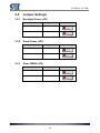
2.5
Jumper Settings
2.5.1
Backlight Power (JP1)
2.5.2
2.5.3
Function
Setting
Jumper
+12V
1-2 closed
+5V (Default)
2-3 closed
Panel Power (JP2)
Function
Setting
Jumper
+3.3V (Default)
1-2 closed
+5V
2-3 closed
Clear CMOS (JP8)
Function
Setting
Jumper
Normal (Default)
1-2 closed
Clear CMOS
2-3 closed
26
CT-DBT0x 3.5’’ SBC
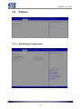
3. Features & Interfaces
3.1
Processor
The cPCI-3620 Series supports the Intel® Atom™ processor E3800 Series
which utilizes 22nm process technology with 3-D Tri-Gate transistors to deliver
significant improvement in computational performance and energy-efficiency.
Based on a new micro-architecture, the processor is designed for a one-chip
platform. This system-on-chip (SoC) solution platform brings enhanced
graphics, greater performance, lower cost, easier validation, and improved x-y
footprint to a broad range of intelligent systems. The processor includes an
Integrated Display Engine, Processor Graphics and Integrated Memory
Controller.
3.2
BIOS
AMI uEFI BIOS on 8MB SPI Flash ROM is used on the CT-DBT0x.
3.3
System Memory
The Integrated Memory Controller (IMC) of the processor supports single
channel, non-ECC, unbuffered DDR3L-1333 memory up to 4 GB with data
transfer rates up to 1333MT/s.
3.4
Graphics
The graphics is integrated in the processor and based on Intel® HD Graphics
4000 technology, enabling substantial gains in performance and lower power
consumption.
•
•
•
•
•
•
DirectX 11 support
OpenGL 4.0 support
Graphics Base Frequency: 542 MHz
Graphics Max Dynamic Frequency: 792 MHz
Full HD video playback
Maximum resolution of 2560x1600@60Hz
LVDS support is provided by a Realtek RTD2136R-CG DP-to-LVDS converter
with dual channel 24-bit output up to 1920x1200 resolution.
27
CT-DBT0x 3.5’’ SBC
3.5
USB
The CT-DBT0x supports 1x USB 3.0 and 1x USB 2.0 external ports, and 4x
internal USB 2.0 ports.
3.6
Ethernet
The CT-DBT0x features 1x 10/100/1000BASE-TX Ethernet by Intel I210IT
GbE Controller supporting WOL/PXE.
3.7
SATA
The CT-DBT0x supports 2x SATA 3Gb/s ports.
3.8
Audio
The CT-DBT0x supports HD audio via Realtek ALC886 codec.
3.9
Expansion
The CT-DBT0x provides the following expansion interfaces.
¾ 2x Mini-PCle slots
• Mini PCIe slot #1: PCIe x1 only or mSATA only
• Mini PCIe slot #2: PCIe x1 & USB 2.0
¾ 1x microSD card slot
¾ 1x SIM card slot
28
CT-DBT0x 3.5’’ SBC
3.10 General Purpose Input Output
GPI and GPO pins may be implemented as GPIO. GPI and GPO pins may be
implemented as SDIO.
Signal
I/O
Description
GPO[0:3]
O
GPI[0:3]
I
General purpose output pins. Upon a hardware
reset, these outputs should be low.
General purpose input pins. Pulled high
internally on the Module.
3.10.1 GPIO Configuration
Board Design
Pin#
GPIO#
Default Configuration
1
―
VCC3
2
―
GND
3
DIO_PH_OUT0
GPO0
4
DIO_PH_IN0
GPI0
5
DIO_PH_OUT1
GPO1
6
DIO_PH_IN1
GPI1
7
DIO_PH_OUT2
GPO2
8
DIO_PH_IN2
GPI2
9
DIO_PH_OUT3
GPO3
10
DIO_PH_IN3
GPI3
Notes
1.
Output pin default setting is “HIGH”
The GPIO function is provided by a Fintek F81866 AD-I, and it can be
accessed through its GPIO index/data port. The index port is the base address
+0 and the data port is the base address +1. To access the GPIO register,
write index to the index port, and then read/write from/to data port. The
configuration on the CT-DBT0x is described as below.
Index Port
0xA00
Data Port
0xA01
29
CT-DBT0x 3.5’’ SBC
Registers Description
GPIO Input/Output Select
GPIO8x Configuration Registers
(Index port=0xA00, Data port=0xA01, Offset=0x88)
Bit 7
Bit 6
Bit 5
Bit 4
Bit 3
Bit 2
Bit 1
Bit 0
GPO3
GPO2
GPO1
GPO0
GPI3
GPI2
GPI1
GPI0
Note.
Bit X = 0 means Input Mode
Bit X = 1 means Output Mode
GPIO Output Data Select
z
GPIO Output Data Register
(Index port=0xA00, Data port=0xA01, Offset=0x89)
Bit 7
Bit 6
Bit 5
Bit 4
Bit 3
Bit 2
Bit 1
Bit 0
GPO3
GPO2
GPO1
GPO0
GPI3
GPI2
GPI1
GPI0
Note.
Bit X = 0 outputs 0 when in output mode
Bit X = 1 outputs 1 when in output mode
30
CT-DBT0x 3.5’’ SBC
3.11 Watchdog Timer
3.11.1 Board Design
The Watchdog Timer (WDT) is implemented by Fintek F81866AD-I.
Register
Address
WDT Base Address
0xA10
3.11.2 Psuedo Code
Set WDT Time Unit (Second Unit)
Step1: ByteData = ReadIOByte(0xA15)
//Read current setting
Step2: ByteData = ByteData & 0xF7
//Set time unit to “second”
Step3: WriteIOByte(0xA15, ByteData)
//Write back
Set WDT Time Value
Step1: WriteIOByte(0xA16, Time)
//Set watch dog time value
Enable WDT
Step1: ByteData = ReadIOByte(0xA15)
//Read current setting
Step2: ByteData = ByteData | 0x20
//Enable WDT
Step3: WriteIOByte(0xA15, ByteData)
//Write back
31
CT-DBT0x 3.5’’ SBC
4. Driver Installation
The drivers for the CT-DBT0x can be found on the driver DVD included with
the system.
Install the following drivers in the order listed.
1.
2.
3.
4.
5.
6.
7.
8.
Chipset
Graphics
Audio
LAN
USB 3.0
Intel Serial IO
Intel Sideband Fabric Device (Intel MBI)
Intel Trusted Execution Engine (Intel TXE)
32
CT-DBT0x 3.5’’ SBC
5. System BIOS
The system BIOS software is stored on EEPROM. The BIOS provides an
interface to modify the configuration. When the battery is removed, all the
parameters will be reset.
Turn on the computer and press <DEL> or <F2> to enter the setup screens.
System Date: MM/DD/YYYY
System Time: HH:MM:SS
Use Tab to switch between Date and Time elements.
33
CT-DBT0x 3.5’’ SBC
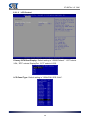
5.1
Advanced
34
CT-DBT0x 3.5’’ SBC
5.1.1
ACPI Settings
Enable ACPI Auto Configuration: Enables or disables BIOS ACPI Auto
Configuration.
Enable Hibernation: Enable or Disable system ability to Hibernate.
ACPI Sleep state: Select the highest ACPI sleep state the system will enter
when the SUSPEND button is pressed. Options: Suspend Disable, S3
(Suspend to RAM).
.
35
CT-DBT0x 3.5’’ SBC
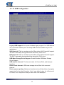
5.1.2
F81866 Super IO Configuration
Enable/disable and configure the serial ports.
5.1.2.1
Serial Port 1 Configuration
Device Type Select: Choose from RS-232, RS-422 and RS-485.
36
CT-DBT0x 3.5’’ SBC
5.1.2.2
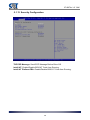
5.1.3
Serial Port 2-4 Configuration
Hardware Monitor
37
CT-DBT0x 3.5’’ SBC
5.1.4
Serial Port Console Redirection
Serial port console redirection settings.
38
CT-DBT0x 3.5’’ SBC
5.1.5
CPU Configuration
Intel Virtualization Technology: When enabled, a VMM can utilize the
additional hardware capabilities provided by Vanderpool Technology
Execute Disable Bit: XP can prevent certain classes of malicious buffer
overflow attacks when combined with a supporting OS (Windows Server 2003
SP1, Windows XP SP2, SusE Linux 9.2, RedHat Enterprise 3 Update 3.)
Power Technology: Configure the power management features.
39
CT-DBT0x 3.5’’ SBC
5.1.6
SATA Configuration
The BIOS automatically detects the presence of SATA device and the
hardware installed in the SATA ports will be showed in the configuration. Each
port can be enabled or disabled individually.
SATA Speed Support: Options: Gen 1, Gen 2.
SATA Mode: Select IDE or AHCI Mode
SATA Port Hot Plug: Enable/disable the port as Hot Pluggable.
40
CT-DBT0x 3.5’’ SBC
5.1.7
Miscellaneous Configuration
OS Selection: Select the OS.
41
CT-DBT0x 3.5’’ SBC
5.1.8
LPSS & SCC Configuration
SCC SD Card Support: Options: Disable, Enable.
LPSS I2C #2 Support: Options: Disable, Enable.
42
CT-DBT0x 3.5’’ SBC
5.1.9
Network Stack Configuration
5.1.10 CSM Configuration
GateA20 Active:
[Upon Request] – GA20 can be disabled using BIOS services.
[Always] – do not allow disabling GA20; this option is useful when any RT
code is executed above 1MB.
43
CT-DBT0x 3.5’’ SBC
Option ROM Message: Set display mode [Force BIOS] or [Keep Current] for
Option ROM.
INT19 Trap Response: BIOS reaction on INT19 trapping by Option ROM:
IMMEDIATE – execute the trap right away; POSTPONED – execute the traps
during legacy boot.
Boot option filter: This option controls what devices system can boot to [UEFI
and Legacy], [Legacy only] or [UEFI only].
Option ROM Execution Order: Controls the execution Option ROM, [Do not
launch], [UEFI only] or [Legacy only].
5.1.11 SDIO Configuration
SDIO Access Mode: Auto Option: Access SD device in DMA mode if
controller supports it, otherwise in PIO mode. DMA Option: Access SD device
in DMA mode. PIO Option: Access SD device in PIO mode.
44
CT-DBT0x 3.5’’ SBC
5.1.12 USB Configuration
Legacy USB Support: Auto option disables legacy support if no USB devices
are connected. Disable option will keep USB devices available only for EFI
applications.
XHCI Hand-off: This is a workaround for OSes without XHCI hand-off support.
The XHCI ownership change should be claimed by XHCI driver.
EHCI Hand-off: This is a workaround for OSes without EHCI hand-off support.
The EHCI ownership change should be claimed by EHCI driver.
USB Mass Storage Driver Support: Enable/Disable USB Mass Storage
Driver Support.
USB transfer time-out: The time-out value for Control, Bulk, and Interrupt
transfers.
Device reset time-out: USB mass storage device Start Unit command
time-out.
Device power-up delay: Maximum time the device will take before it properly
reports itself to the Host Controller. “Auto” uses default value: for a Root port it
is 100ms, for a Hub port the delay is taken from Hub descriptor.
45
CT-DBT0x 3.5’’ SBC
5.1.13 Security Configuration
TXE EOP Message: Send EOP Message Before Enter OS.
Intel® AT: Enable/Disable BIOS AT Code from Running.
Intel® AT Platform PBA: Enable/Disable BIOS AT Code from Running.
46
CT-DBT0x 3.5’’ SBC
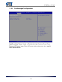
5.2
Chipset
5.2.1
Northbridge Configuration
47
CT-DBT0x 3.5’’ SBC
5.2.1.1
Intel IGD Configuration
IGD Turbo Enable: Enable/Disable: IGD Turbo.
GFX Boost: Enable/Disable GFX Boost.
PAVC: Enable/Disable Protected Audio Video Control.
DVMT Pre-Allocated: Select DVMT 5.0 Pre-Allocated (Fixed) Graphics
Memory size used by the Internal Graphics Device.
DVMT Total Gfx Mem: Select DVMT 5.0 Total Graphics Memory size used by
the Internal Graphics Device.
Aperture Size: Select the Aperture Size.
48
CT-DBT0x 3.5’’ SBC
5.2.1.2
LCD Control
Primary IGFX Boot Display: Default setting is “VBIOS Default”. “CRT”selects
VGA, “EFP” selects DisplayPort, “LFP” selects LVDS.
LCD Panel Type: Default setting is “1024x768 LVDS 24-bit”.
49
CT-DBT0x 3.5’’ SBC
5.2.2
Southbridge Configuration
High Precision Timer: Enable or Disable the High Precision Event Timer.
Restore AC Power Loss: Select AC power state when power is re-applied
after a power failure.
50
CT-DBT0x 3.5’’ SBC
5.2.2.1
USB Configuration
5.2.2.2
PCI Express Configuration
51
CT-DBT0x 3.5’’ SBC
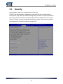
5.3
Security
Administrator’s and User’s passwords could be set.
If ONLY the Administrator’s password is set, then this only limits access to
Setup and is only asked for when entering Setup. If ONLY the User’s password
is set, then this is a power on password and must be entered to boot or enter
Setup. In Setup, the user will have administrator rights. The minimum length of
the password is 3 and the maximum length is 20.
52
CT-DBT0x 3.5’’ SBC
5.3.1
Secure Boot Menu
Secure Boot: Secure Boot can be enabled if the System running in User
mode with enrolled Platform Key (PK) and CSM function is disabled.
Secure Boot Mode: Secure Boot mode selector. ‘Custom’ Mode enables
users to change Image Execution policy and manage Secure Boot Keys.
53
CT-DBT0x 3.5’’ SBC
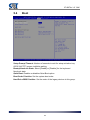
5.4
Boot
Setup Prompt Timeout: Number of seconds to wait for setup activation key.
65535 (0xFFFF) means indefinite waiting.
Bootup NumLock State: Select [Enable] or [Disable] for the keyboard
NumLock state.
Quiet Boot: Enables or disables Quiet Boot option.
Boot Order Priorities: Set the system boot order.
Hard Drive BBS Priorities: Set the order of the legacy devices in this group.
54
CT-DBT0x 3.5’’ SBC
5.5
Save and Exit
55
CT-DBT0x 3.5’’ SBC
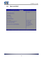
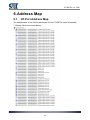
6. Address Map
6.1
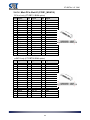
I/O Port Address Map
The assignments of the I/O port addresses for the CT-DBT0x under Windows®
7 Ultimate 64-bit are shown below.
56
CT-DBT0x 3.5’’ SBC
I/O Port Address Map (cont'd)
57
CT-DBT0x 3.5’’ SBC
I/O Port Address Map (cont'd)
58
CT-DBT0x 3.5’’ SBC
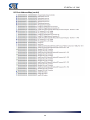
6.2
Interrupt Controller (IRQ) Map
The interrupt controller map for the CT-DBT0x under Windows® 7 Ultimate
64-bit is shown below.
59
CT-DBT0x 3.5’’ SBC
Interrupt Controller (IRQ) Map (cont'd)
60
CT-DBT0x 3.5’’ SBC
Interrupt Controller (IRQ) Map (cont'd)
61
CT-DBT0x 3.5’’ SBC
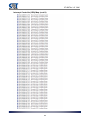
Interrupt Controller (IRQ) Map (cont'd)
62
CT-DBT0x 3.5’’ SBC
Interrupt Controller (IRQ) Map (cont'd)
63
CT-DBT0x 3.5’’ SBC
Interrupt Controller (IRQ) Map (cont'd)
64
CT-DBT0x 3.5’’ SBC
Interrupt Controller (IRQ) Map (cont'd)
65
CT-DBT0x 3.5’’ SBC
Interrupt Controller (IRQ) Map (cont'd)
66
CT-DBT0x 3.5’’ SBC
6.3
Memory Map
The memory map of DRAM for the CT-DBT0x under Windows® 7 Ultimate
64-bit is shown below.
67
CT-DBT0x 3.5’’ SBC
Memory Map (cont'd)
68