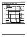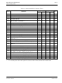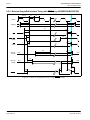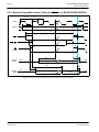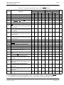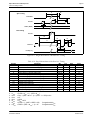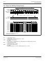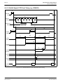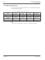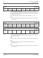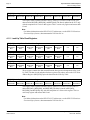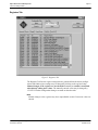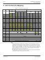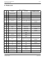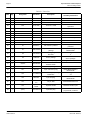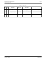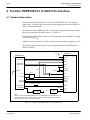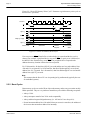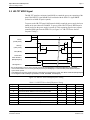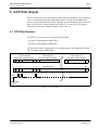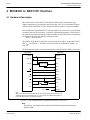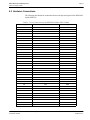
1
SED1376 Embedded Memory LCD Controller SED1376 TECHNICAL MANUAL Document Number: X31B-Q-001-03 Copyright © 2000 Epson Research and Development, Inc. All Rights Reserved. Information in this document is subject to change without notice.You may download and use this document, but only for your own use in evaluating Seiko Epson/EPSON products. You may not modify the document. Epson Research and Development, Inc. disclaims any representation that the contents of this document are accurate or current. The Programs/Technologies described in this document may contain material protected under U.S. and/or International Patent laws. EPSON is a registered trademark of Seiko Epson Corporation. All other trademarks are the property of their respective owners. Page 2 Epson Research and Development Vancouver Design Center THIS PAGE LEFT BLANK SED1376 X31B-Q-001-03 TECHNICAL MANUAL Issue Date: 00/07/24 Epson Research and Development Vancouver Design Center Page 3 COMPREHENSIVE SUPPORT TOOL S EPSON provides the designer and manufacturer a complete set of resources and tools for the development of LCD Graphics Systems. Documentation • Technical manuals • Evaluation/Demonstration board manual Evaluation/Demonstration Board • • • • • • • Assembled and fully tested Graphics Evaluation/Demonstration board Schematic of Evaluation/Demonstration board Parts List Installation Guide CPU Independent Software Utilities Evaluation Software Windows CE Display Driver Application Engineering Support EPSON offers the following services through their Sales and Marketing Network: • Sales Technical Support • Customer Training • Design Assistance Application Engineering Support Engineering and Sales Support is provided by: Japan Seiko Epson Corporation Electronic Devices Marketing Division 421-8, Hino, Hino-shi Tokyo 191-8501, Japan Tel: 042-587-5812 Fax: 042-587-5564 http://www.epson.co.jp Hong Kong Epson Hong Kong Ltd. 20/F., Harbour Centre 25 Harbour Road Wanchai, Hong Kong Tel: 2585-4600 Fax: 2827-4346 TECHNICAL MANUAL Issue Date: 00/07/24 North America Epson Electronics America, Inc. 150 River Oaks Parkway San Jose, CA 95134, USA Tel: (408) 922-0200 Fax: (408) 922-0238 http://www.eea.epson.com Taiwan Epson Taiwan Technology & Trading Ltd. 10F, No. 287 Nanking East Road Sec. 3, Taipei, Taiwan Tel: 02-2717-7360 Fax: 02-2712-9164 Europe Epson Europe Electronics GmbH Riesstrasse 15 80992 Munich, Germany Tel: 089-14005-0 Fax: 089-14005-110 Singapore Epson Singapore Pte., Ltd. No. 1 Temasek Avenue #36-00 Millenia Tower Singapore, 039192 Tel: 337-7911 Fax: 334-2716 SED1376 X31B-Q-001-03 Page 4 Epson Research and Development Vancouver Design Center THIS PAGE LEFT BLANK SED1376 X31B-Q-001-03 TECHNICAL MANUAL Issue Date: 00/07/24 Epson Research and Development Vancouver Design Center Page 5 Table of Contents INTRODUCTION SED1376 Embedded Memory LCD Controller Product Brief SPECIFICATION SED1376 Hardware Functional Specification PROGRAMMER’S REFERENCE SED1376 Programming Notes and Examples SED1376 Register Summary UTILITIES 1376CFG Configuration Program 1376SHOW Demonstration Program 1376PLAY Diagnostic Utility 1376BMP Demonstration Program DRIVERS SED1376 Windows® CE Display Drivers SED13XX 32-Bit Windows Device Driver Installation Guide EVALUATION SDU1376B0C Rev. 1.0 Evaluation Board User Manual APPLICATION NOTES Interfacing to the Toshiba MIPS TMPR3905/3912 Microprocessor Interfacing to the PC Card Bus Power Consumption Interfacing to the NEC VR4102/VR4111 Microprocessor Interfacing to the NEC VR4181 Microprocessor Interfacing to the Motorola MPC821 Microprocessor Interfacing to the Motorola MCF5307 "Coldfire" Microprocessor Connecting to the Sharp HR-TFT Panels Connecting to the Epson D-TFD Panels Interfacing to the Motorola MC68030 Microprocessor Interfacing to the Motorola RedCap2 DSP with Integrated MCU Interfacing to 8-bit Processors Interfacing to the Motorola MC68VZ328 Dragonball Microprocessor TECHNICAL MANUAL Issue Date: 00/07/24 SED1376 X31B-Q-001-03 Page 6 Epson Research and Development Vancouver Design Center THIS PAGE LEFT BLANK SED1376 X31B-Q-001-03 TECHNICAL MANUAL Issue Date: 00/07/24 ENERGY S AV I N G GRAPHICS EPSON SED1376 July 2000 SED1376 Embedded Memory LCD Controller The SED1376 is a color/monochrome LCD graphics controller with an embedded 80K byte SRAM display buffer. While supporting all other panel types, the SED1376 is the only LCD controller to directly interface to both the Epson D-TFD and the Sharp HR-TFT family of products thus removing the requirement of an external Timing Control IC. This high level of integration provides a low cost, low power, single chip solution to meet the demands of embedded markets such as Mobile Communications devices and Palm-size PCs, where board size and battery life are major concerns. The SED1376 utilizes a guaranteed low-latency CPU architecture thus providing support for microprocessors without READY/WAIT# handshaking signals. The 32-bit internal data path provides high performance bandwidth into display memory allowing for fast screen updates. Products requiring a rotated display image can take advantage of the SwivelViewTM feature which provides hardware rotation of the display memory transparent to the software application. The SED1376 also provides support for “Picture-in-Picture Plus” (a variable size Overlay window). The SED1376 provides impressive support for Palm OS handhelds, however its impartiality to CPU type or operating system makes it an ideal display solution for a wide variety of applications. ■ FEATURES • Embedded Display Buffer. • Low Operating Voltage. • Low-latency CPU interface. • Direct support for the multiple CPU types. • Programmable Resolutions and Color depths. • STN LCD support. • Active Matrix LCD support. • Reflective Active Matrix support. • SwivelViewTM (90, 180, 270° hardware rotation of displayed image). • • • • • “Picture-in-Picture Plus”. Software Initiated Power Save Mode. Hardware or Software Video Invert. 100-pin TQFP15 package. 104-pin CFLGA package. ■ SYSTEM BLOCK DIAGRAM CPU Data and Control Signals SED1376 Digital Out Flat Panel X31B-C-001-02 1 GRAPHICS SED1376 ■ DESCRIPTION Memory Interface • Display Modes Embedded 80K byte SRAM display buffer. CPU Interface • • ‘Fixed’ low-latency CPU access times. Direct support for: Hitachi SH-4 / SH-3. Motorola M68xxx (REDCAP2, DragonBall, ColdFire) . MPU bus interface with programmable READY. • 4/8-bit monochrome LCD interface. 4/8/16-bit color STN LCD interface. Single-panel, single-drive passive displays. 9/12/18-bit Active matrix TFT interface. ‘Direct’ support for Epson D-TFD and Sharp HR-TFT (external timing control IC not required). Typical resolutions supported: - 320x240@8bpp - 160x160 @16bpp - 160x240 @16bpp • 1/2/4/8/16 bit-per-pixel (bpp) support. Up to 64 gray shades using FRM and dithering on monochrome passive LCD panels. Up to 64K colors on passive STN panels. Up to 64K colors on active matrix panels. SwivelView: direct hardware rotation of display image by 90°, 180°, 270°. “Picture-in-Picture Plus”: displays a variable size window overlaid over background image. Double Buffering/multi-pages: provides smooth animation and instantaneous screen update. Power Down Modes • Software Initiated Power Save Mode. Operating Voltage • COREVDD 1.8 to 2.2 volts and 3.0 to 3.6 volts. • HIOVDD 1.8 to 2.2 volts and 3.0 to 3.6 volts. • NIOVDD 3.0 to 3.6 volts. Package Clock Source • • • • • • Display Support • • • • • • • Two clock inputs (single clock possible). Clock source can be internally divided down for a higher frequency clock input. • • 100-pin TQFP15. 104-pin CFLGA. CONTACT YOUR SALES REPRESENTATIVE FOR THESE COMPREHENSIVE DESIGN TOOLS • SED1376 Technical Manual • SDU1376 Evaluation Boards • CPU Independent Software Utilities Japan Seiko Epson Corporation Electronic Devices Marketing Division 421-8, Hino, Hino-shi Tokyo 191-8501, Japan Tel: 042-587-5812 Fax: 042-587-5564 http://www.epson.co.jp Hong Kong Epson Hong Kong Ltd. 20/F., Harbour Centre 25 Harbour Road Wanchai, Hong Kong Tel: 2585-4600 Fax: 2827-4346 • Palm OS Hardware Abstraction Layer • Windows CE Display Driver • VXWorks TornadoTM Display Driver North America Epson Electronics America, Inc. 150 River Oaks Parkway San Jose, CA 95134, USA Tel: (408) 922-0200 Fax: (408) 922-0238 http://www.eea.epson.com Taiwan Epson Taiwan Technology & Trading Ltd. 10F, No. 287 Nanking East Road Sec. 3, Taipei, Taiwan Tel: 02-2717-7360 Fax: 02-2712-9164 Europe Epson Europe Electronics GmbH Riesstrasse 15 80992 Munich, Germany Tel: 089-14005-0 Fax: 089-14005-110 Singapore Epson Singapore Pte., Ltd. No. 1 Temasek Avenue #36-00 Millenia Tower Singapore, 039192 Tel: 337-7911 Fax: 334-2716 VDC Copyright © 2000 Epson Research and Development, Inc. All rights reserved. Information in this document is subject to change without notice. You may download and use this document, but only for your own use in evaluating Seiko Epson/ EPSON products. You may not modify the document. Epson Research and Development, Inc. disclaims any representation that the contents of this document are accurate or current. The Programs/Technologies described in this document may contain material protected under U.S. and/or International Patent laws. EPSON is a registered trademark of Seiko Epson Corporation. Palm Computing is a registered trademark and the Palm OS platform Platinum logo is a trademark of Palm Computing, Inc., 3Com or its subsidiaries. Microsoft, Windows, and the Windows CE Logo are registered trademarks of Microsoft Corporation . All other trademarks are the property of their respective owners. 2 X31B-C-001-02 SED1376 Embedded Memory LCD Controller Hardware Functional Specification Document Number: X31B-A-001-04 Copyright © 1999, 2000 Epson Research and Development, Inc. All Rights Reserved. Information in this document is subject to change without notice.You may download and use this document, but only for your own use in evaluating Seiko Epson/EPSON products. You may not modify the document. Epson Research and Development, Inc. disclaims any representation that the contents of this document are accurate or current. The Programs/Technologies described in this document may contain material protected under U.S. and/or International Patent laws. EPSON is a registered trademark of Seiko Epson Corporation. All other Trademarks are the property of their respective owners Page 2 Epson Research and Development Vancouver Design Center THIS PAGE LEFT BLANK SED1376 X31B-A-001-04 Hardware Functional Specification Issue Date: 00/08/10 Epson Research and Development Vancouver Design Center Page 3 Table of Contents 1 Introduction . . . . . . . . . . . . . . . . . . . . . . . . . . . . . . . . . . . . . . . 11 1.1 Scope . . . . . . . . . . . . . . . . . . . . . . . . . . . . . . . . . . 11 1.2 Overview Description . . . . . . . . . . . . . . . . . . . . . . . . . . . 11 2 Features . . . . . . . . . . 2.1 Integrated Frame Buffer 2.2 CPU Interface . . . . 2.3 Display Support . . . . 2.4 Display Modes . . . . 2.5 Display Features . . . 2.6 Clock Source . . . . . 2.7 Miscellaneous . . . . 3 Typical System Implementation Diagrams . . . . . . . . . . . . . . . . . . . . . . 14 4 Pins . . . . . . . . . . . . . . . . . 4.1 Pinout Diagram - TQFP15 - 100pin 4.2 Pinout Diagram - CFLGA - 104pin 4.3 Pin Descriptions . . . . . . . 4.3.1 Host Interface . . . . . . . . 4.3.2 LCD Interface . . . . . . . . 4.3.3 Clock Input . . . . . . . . . 4.3.4 Miscellaneous . . . . . . . . 4.3.5 Power And Ground . . . . . 4.4 Summary of Configuration Options 4.5 Host Bus Interface Pin Mapping . 4.6 LCD Interface Pin Mapping . . . 5 D.C. Characteristics . . . . . . . . . . . . . . . . . . . . . . . . . . . . . . . . . . 29 6 A.C. Characteristics . . . . . . . . . . . . . . . . . . . . . . . . . . . . . . . . . . 6.1 Clock Timing . . . . . . . . . . . . . . . . . . . . . . . . . . . . . . 6.1.1 Input Clocks . . . . . . . . . . . . . . . . . . . . . . . . . . . . . . . . . . . . . . 6.1.2 Internal Clocks . . . . . . . . . . . . . . . . . . . . . . . . . . . . . . . . . . . . 6.2 CPU Interface Timing . . . . . . . . . . . . . . . . . . . . . . . . . . . 6.2.1 Generic #1 Interface Timing . . . . . . . . . . . . . . . . . . . . . . . . . . . . . 6.2.2 Generic #2 Interface Timing (e.g. ISA) . . . . . . . . . . . . . . . . . . . . . . . . 6.2.3 Hitachi SH-4 Interface Timing . . . . . . . . . . . . . . . . . . . . . . . . . . . . 6.2.4 Hitachi SH-3 Interface Timing . . . . . . . . . . . . . . . . . . . . . . . . . . . . 6.2.5 Motorola MC68K #1 Interface Timing (e.g. MC68000) . . . . . . . . . . . . . . . 6.2.6 Motorola MC68K #2 Interface Timing (e.g. MC68030) . . . . . . . . . . . . . . . Hardware Functional Specification Issue Date: 00/08/10 . . . . . . . . . . . . . . . . . . . . . . . . . . . . . . . . . . . . . . . . . . . . . . . . . . . . . . . . . . . . . . . . . . . . . . . . . . . . . . . . . . . . . . . . . . . . . . . . . . . . . . . . . . . . . . . . . . . . . . . . . . . . . . . . . . . . . . . . . . . . . . . . . . . . . . . . . . . . . . . . . . . . . . . . . . . . . . . . . . . . . . . . . . . . . . . . . . . . . . . . . . . . . . . . . . . . . . . . . . . . . . . . . . . . . . . . . . . . . . . . . . . . . . . . . . . . . . . . . . . . . . . . . . . . . . . . . . . . . . . . . . . . . . . . . . . . . . . . . . . . . . . . . . . . . . . . . . . . . . . . . . . . . . . . . . . . . . . . . . . . . . . 12 . 12 . 12 . 12 . 13 . 13 . 13 . 13 . . . . . . . . . . . . . . . . . . . . . . . . . . . . . . . . . . . . . . . . . . . . . . . . . . . . . . . . . . . . . . . . . . . . . . . . . . . . . . . . . . . . . . . . . . . . . . . . . . . . . . . . . . . . . . . . . . . . . . . . . . . . . . . . . . . . . . . . . . . . . . . . . . . . . . . . . . . . . . . . . . . . . . 18 18 19 20 20 23 25 25 25 26 27 28 30 30 30 31 32 32 34 36 38 40 42 SED1376 X31B-A-001-04 Page 4 Epson Research and Development Vancouver Design Center 6.2.7 6.2.8 Motorola REDCAP2 Interface Timing . . . . . . . . . . . . . Motorola DragonBall Interface Timing with DTACK (e.g. MC68EZ328/MC68VZ328) . . . . . . . . . . . . . . . . 6.2.9 Motorola DragonBall Interface Timing w/o DTACK (e.g. MC68EZ328/MC68VZ328) . . . . . . . . . . . . . . . . 6.3 LCD Power Sequencing . . . . . . . . . . . . . . . . . . 6.3.1 Passive/TFT Power-On Sequence . . . . . . . . . . . . . . . . 6.3.2 Passive/TFT Power-Off Sequence . . . . . . . . . . . . . . . . 6.3.3 Power Save Status . . . . . . . . . . . . . . . . . . . . . . . . 6.4 Display Interface . . . . . . . . . . . . . . . . . . . . . 6.4.1 Generic STN Panel Timing . . . . . . . . . . . . . . . . . . . 6.4.2 Single Monochrome 4-Bit Panel Timing . . . . . . . . . . . . 6.4.3 Single Monochrome 8-Bit Panel Timing . . . . . . . . . . . . 6.4.4 Single Color 4-Bit Panel Timing . . . . . . . . . . . . . . . . 6.4.5 Single Color 8-Bit Panel Timing (Format 1) . . . . . . . . . . 6.4.6 Single Color 8-Bit Panel Timing (Format 2) . . . . . . . . . . 6.4.7 Single Color 16-Bit Panel Timing . . . . . . . . . . . . . . . . 6.4.8 Generic TFT Panel Timing . . . . . . . . . . . . . . . . . . . 6.4.9 9/12/18-Bit TFT Panel Timing . . . . . . . . . . . . . . . . . 6.4.10 160x160 Sharp HR-TFT Panel Timing (e.g. LQ031B1DDxx) . 6.4.11 320x240 Sharp HR-TFT Panel Timing (e.g. LQ039Q2DS01) . 6.4.12 160x240 Epson D-TFD Panel Timing (e.g. LF26SCR) . . . . . 6.4.13 320x240 Epson D-TFD Panel Timing (e.g. LF37SQR) . . . . . . . . . . . . . . . . 46 . . . . . . . . . . . . . . . . . . . . . . . . . . . . . . . . . . . . . . . . . . . . . . . . . . . . . . . . . . . . . . . . . . . . . . . . . . . . . . . . . . . . . . . . . . . . . . . . . . . . . . . . . . . . . . . . . . . . . . . . . . . . . . . . . . . . . . . . . . . . . . . . . . . . . . . . . . . . . . . . . . . . . . . . . 48 . . 50 . . 50 . . 51 . . 52 . .53 . . 54 . . 56 . . 58 . . 60 . . 62 . . 64 . . 66 . . 68 . . 69 . . 72 . . 76 . . 78 . . 82 7 Clocks . . . . . . . . . . . 7.1 Clock Descriptions . . 7.1.1 BCLK . . . . . . 7.1.2 MCLK . . . . . . 7.1.3 PCLK . . . . . . 7.1.4 PWMCLK . . . . 7.2 Clock Selection . . . 7.3 Clocks versus Functions . . . . . . . . . . . . . . . . . . . . . . . . . . . . . . . . . . . . . . . . . . . . . . . . . . . . . . . . . . . . . . . . . . . . . . . . . . . . . . . . . . . . . . . . . . . . . . . . . . . . . . . . . . . . . . . . . . . . . . . . . . . . . . . . . . . . . . . . . . . . . . . . . . . . . . . . . . . . . . . . . . . . . . . . . . . . . . . . . . . . . . . . . . . . . . . . . . . . . . . . . . . . . . . . . . . . . . . . . . . . . . . . . . . . . . . . . . . . . . 86 .86 . 86 . 86 . 87 . 88 . 89 . 90 8 Registers . . . . . . . . . . . . . . . . . 8.1 Register Mapping . . . . . . . . . 8.2 Register Set . . . . . . . . . . . . 8.3 Register Descriptions . . . . . . . . 8.3.1 Read-Only Configuration Registers 8.3.2 Clock Configuration Registers . . 8.3.3 Look-Up Table Registers . . . . . 8.3.4 Panel Configuration Registers . . . 8.3.5 Display Mode Registers . . . . . . . . . . . . . . . . . . . . . . . . . . . . . . . . . . . . . . . . . . . . . . . . . . . . . . . . . . . . . . . . . . . . . . . . . . . . . . . . . . . . . . . . . . . . . . . . . . . . . . . . . . . . . . . . . . . . . . . . . . . . . . . . . . . . . . . . . . . . . . . . . . . . . . . . . . . . . . . . . . . . . . . . . . . . . . . . . . . 91 . 91 . 92 .93 . 93 . 94 . 95 . 98 .105 SED1376 X31B-A-001-04 . . . . . . . . . . . . . . . . . . . 44 . . . . . . . . . . . . . . . . . . . . . . . . . . . . . . . . . Hardware Functional Specification Issue Date: 00/08/10 Epson Research and Development Vancouver Design Center 8.3.6 8.3.7 8.3.8 8.3.9 9 Page 5 Picture-in-Picture Plus Registers . . . . . . . . . . . . . . . . . . . . . Miscellaneous Registers . . . . . . . . . . . . . . . . . . . . . . . . . . General IO Pins Registers . . . . . . . . . . . . . . . . . . . . . . . . . Pulse Width Modulation (PWM) Clock and Contrast Voltage (CV) Pulse Configuration Registers . . . . . . . . . . . . . . . . . . . . . . . . . . Frame Rate Calculation 10 Display Data Formats . . . . . .110 . . . . . .115 . . . . . .116 . . . . . .121 . . . . . . . . . . . . . . . . . . . . . . . . . . . . . . . . 125 . . . . . . . . . . . . . . . . . . . . . . . . . . . . . . . . . 126 11 Look-Up Table Architecture . . . . . . . . . . . . . . . . . . . . . . . . . . . . . . 127 11.1 Monochrome Modes . . . . . . . . . . . . . . . . . . . . . . . . . . . . 127 11.2 Color Modes . . . . . . . . . . . . . . . . . . . . . . . . . . . . . . . 129 12 SwivelView™ . . . . . . . . . . . . 12.1 Concept . . . . . . . . . . . 12.2 90° SwivelView™ . . . . . . 12.2.1 Register Programming . . . 12.3 180° SwivelView™ . . . . . . 12.3.1 Register Programming . . . 12.4 270° SwivelView™ . . . . . . 12.4.1 Register Programming . . . . . . . . . . . . . . . . . . . . . . . . . . . . . . . . . . . . . . . . . . . . . . . . . . . . . . . . . . . . . . . . . . . . . . . . . . . . . . . . . . . . . . . . . . . . . . . . . . . . . . . . . . . . . . . . . . . . . . . . . . . . . . . . . . . . . . . . . . . . . . . . . . . . . . . . . . . . . . . . . . . . . . . . . . . . . . . . . . . . . . . . . . . 133 . . 133 . . 133 . . .134 . . 135 . . .135 . . 136 . . .137 13 Picture-in-Picture Plus . . . . . . . 13.1 Concept . . . . . . . . . . . 13.2 With SwivelView Enabled . . . 13.2.1 SwivelView 90° . . . . . . . 13.2.2 SwivelView 180° . . . . . . 13.2.3 SwivelView 270° . . . . . . . . . . . . . . . . . . . . . . . . . . . . . . . . . . . . . . . . . . . . . . . . . . . . . . . . . . . . . . . . . . . . . . . . . . . . . . . . . . . . . . . . . . . . . . . . . . . . . . . . . . . . . . . . . . . . . . . . . . . . . . . . . . . . . . . . . . . . . . . . . . . . . . 138 . . 138 . . 139 . . .139 . . .139 . . .140 14 Big-Endian Bus Interface . . . . . 14.1 Byte Swapping Bus Data . . . . 14.1.1 16 Bpp Color Depth . . . . . 14.1.2 1/2/4/8 Bpp Color Depth . . . . . . . . . . . . . . . . . . . . . . . . . . . . . . . . . . . . . . . . . . . . . . . . . . . . . . . . . . . . . . . . 141 . . 141 . . .142 . . .143 . . . . . . . . . . . . . . . . . . . . . . . . . . . . . . . . . . . . 15 Power Save Mode . . . . . . . . . . . . . . . . . . . . . . . . . . . . . . . . . . . . 144 16 Mechanical Data . . . . . . . . . . . . . . . . . . . . . . . . . . . . . . . . . . . . 145 17 References . . . . . . . . . . . . . . . . . . . . . . . . . . . . . . . . . . . . . . . 147 18 Technical Support . . . . . . . . . . . . . . . . . . . . . . . . . . . . . . . . . . . 148 Hardware Functional Specification Issue Date: 00/08/10 SED1376 X31B-A-001-04 Page 6 Epson Research and Development Vancouver Design Center THIS PAGE LEFT BLANK SED1376 X31B-A-001-04 Hardware Functional Specification Issue Date: 00/08/10 Epson Research and Development Vancouver Design Center Page 7 List of Tables Table 4-1: CFLGA Pin Mapping . . . . . . . . . . . . . . . . . . . . . . . . . . Table 4-2: Host Interface Pin Descriptions . . . . . . . . . . . . . . . . . . . . . Table 4-3: LCD Interface Pin Descriptions . . . . . . . . . . . . . . . . . . . . . Table 4-4: Clock Input Pin Descriptions. . . . . . . . . . . . . . . . . . . . . . . Table 4-5: Miscellaneous Pin Descriptions . . . . . . . . . . . . . . . . . . . . . Table 4-6: Power And Ground Pin Descriptions . . . . . . . . . . . . . . . . . . Table 4-7: Summary of Power-On/Reset Options . . . . . . . . . . . . . . . . . . Table 4-8: Host Bus Interface Pin Mapping . . . . . . . . . . . . . . . . . . . . . Table 4-9: LCD Interface Pin Mapping . . . . . . . . . . . . . . . . . . . . . . . Table 5-1: Absolute Maximum Ratings . . . . . . . . . . . . . . . . . . . . . . . Table 5-2: Recommended Operating Conditions . . . . . . . . . . . . . . . . . . Table 5-3: Electrical Characteristics for VDD = 3.3V typical. . . . . . . . . . . . Table 6-1: Clock Input Requirements for CLKI when CLKI to BCLK divide > 1 . Table 6-2: Clock Input Requirements for CLKI when CLKI to BCLK divide = 1 . Table 6-3: Clock Input Requirements for CLKI2 . . . . . . . . . . . . . . . . . . Table 6-4: Internal Clock Requirements . . . . . . . . . . . . . . . . . . . . . . . Table 6-5: Generic #1 Interface Timing . . . . . . . . . . . . . . . . . . . . . . . Table 6-6: Generic #2 Interface Timing . . . . . . . . . . . . . . . . . . . . . . . Table 6-7: Hitachi SH-4 Interface Timing . . . . . . . . . . . . . . . . . . . . . . Table 6-8: Hitachi SH-3 Interface Timing . . . . . . . . . . . . . . . . . . . . . . Table 6-9: Motorola MC68K #1 Interface Timing . . . . . . . . . . . . . . . . . Table 6-10: Motorola MC68K #2 Interface Timing . . . . . . . . . . . . . . . . . Table 6-11: Motorola REDCAP2 Interface Timing. . . . . . . . . . . . . . . . . . Table 6-12: Motorola DragonBall Interface with DTACK Timing . . . . . . . . . . Table 6-13: Motorola DragonBall Interface without DTACK Timing . . . . . . . . Table 6-14: Passive/TFT Power-On Sequence Timing . . . . . . . . . . . . . . . . Table 6-15: Passive/TFT Power-Off Sequence Timing . . . . . . . . . . . . . . . . Table 6-16: Power Save Status Timing . . . . . . . . . . . . . . . . . . . . . . . . Table 6-17: Panel Timing Parameter Definition and Register Summary . . . . . . . Table 6-18: Single Monochrome 4-Bit Panel A.C. Timing . . . . . . . . . . . . . . Table 6-19: Single Monochrome 8-Bit Panel A.C. Timing . . . . . . . . . . . . . . Table 6-20: Single Color 4-Bit Panel A.C. Timing . . . . . . . . . . . . . . . . . . Table 6-21: Single Color 8-Bit Panel A.C. Timing (Format 1) . . . . . . . . . . . . Table 6-22: Single Color 8-Bit Panel A.C. Timing (Format 2) . . . . . . . . . . . . Table 6-23: Single Color 16-Bit Panel A.C. Timing . . . . . . . . . . . . . . . . . Table 6-24: TFT A.C. Timing . . . . . . . . . . . . . . . . . . . . . . . . . . . . . Table 6-25: 160x160 Sharp HR-TFT Horizontal Timing . . . . . . . . . . . . . . . Hardware Functional Specification Issue Date: 00/08/10 . . . . . . . . . . . . . . . . . . . . . . . . . . . . . . . . . . . . . . . . . . . . . . . . . . . . . . . . . . . . . . . . . . . . . . . . . . . . . . . . . . . . . . . . . . . . . . . . . . . . . . . . . . . . . . . . . . . . . . . . . . . . . . . . . . . . . . . . . . . . . . . . . . . . . . . . . . . . . . . . . . . . . . . . . . . . . . . . . . . . . . . . . . . . . . . . . . . . . . . . . . . . . . . . . . . . . . . . . . . . . . . . . . . . . . . . . . . . . . . . . . . . . . . . . . . . . . . . . . . . . . . . . . . . . . . . . . . . . . . . . . . . . . . . . . . . . . . . . . . . . . . . . . . . . . . . . . . . . . . . . . . . . . . . . . . . . 19 20 23 25 25 25 26 27 28 29 29 29 30 31 31 31 33 35 37 39 41 43 45 47 49 50 51 52 53 57 59 61 63 65 67 71 73 SED1376 X31B-A-001-04 Page 8 Table 6-26: 160x160 Sharp HR-TFT Panel Vertical Timing . . . . Table 6-27: 320x240 Sharp HR-TFT Panel Horizontal Timing. . . Table 6-28: 320x240 Sharp HR-TFT Panel Vertical Timing . . . . Table 6-29: 160x240 Epson D-TFD Panel Horizontal Timing . . . Table 6-30: 160x240 Epson D-TFD Panel GCP Horizontal Timing Table 6-31: 160x240 Epson D-TFD Panel Vertical Timing . . . . Table 6-32: 320x240 Epson D-TFD Panel Horizontal Timing . . . Table 6-33: 320x240 Epson D-TFD Panel GCP Horizontal Timing Table 6-34: 320x240 Epson D-TFD Panel Vertical Timing . . . . Table 7-1: BCLK Clock Selection . . . . . . . . . . . . . . . . . Table 7-2: MCLK Clock Selection. . . . . . . . . . . . . . . . . Table 7-3: PCLK Clock Selection . . . . . . . . . . . . . . . . . Table 7-4: Relationship between MCLK and PCLK. . . . . . . . Table 7-5: PWMCLK Clock Selection. . . . . . . . . . . . . . . Table 7-6: SED1376 Internal Clock Requirements . . . . . . . . Table 8-1: SED1376 Register Set . . . . . . . . . . . . . . . . . Table 8-2: MCLK Divide Selection . . . . . . . . . . . . . . . . Table 8-3: PCLK Divide Selection. . . . . . . . . . . . . . . . . Table 8-4: PCLK Source Selection. . . . . . . . . . . . . . . . . Table 8-5: Panel Data Width Selection . . . . . . . . . . . . . . Table 8-6: Active Panel Resolution Selection . . . . . . . . . . . Table 8-7: LCD Panel Type Selection . . . . . . . . . . . . . . . Table 8-8: Inverse Video Mode Select Options . . . . . . . . . . Table 8-9: LCD Bit-per-pixel Selection . . . . . . . . . . . . . . Table 8-10: SwivelViewTM Mode Select Options . . . . . . . . . Table 8-11: 32-bit Address Increments for Color Depth . . . . . . Table 8-12: 32-bit Address Increments for Color Depth . . . . . . Table 8-13: 32-bit Address Increments for Color Depth . . . . . . Table 8-14: 32-bit Address Increments for Color Depth . . . . . . Table 8-15: PWM Clock Control . . . . . . . . . . . . . . . . . . Table 8-16: CV Pulse Control . . . . . . . . . . . . . . . . . . . . Table 8-17: PWM Clock Divide Select Options . . . . . . . . . . Table 8-18: CV Pulse Divide Select Options . . . . . . . . . . . . Table 8-19: PWMOUT Duty Cycle Select Options . . . . . . . . . Table 15-1: Power Save Mode Function Summary . . . . . . . . . SED1376 X31B-A-001-04 Epson Research and Development Vancouver Design Center . . . . . . . . . . . . . . . . . . . . . . . . . . . . . . . . . . . . . . . . . . . . . . . . . . . . . . . . . . . . . . . . . . . . . . . . . . . . . . . . . . . . . . . . . . . . . . . . . . . . . . . . . . . . . . . . . . . . . . . . . . . . . . . . . . . . . . . . . . . . . . . . . . . . . . . . . . . . . . . . . . . . . . . . . . . . . . . . . . . . . . . . . . . . . . . . . . . . . . . . . . . . . . . . . . . . . . . . . . . . . . . . . . . . . . . . . . . . . . . . . . . . . . . . . . . . . . . . . . . . . . . . . . . . . . . . . . . . . . . . . . . . . . . . . . . . . . . . . . . . . . . . . . . . . . . . . . . . . . . . . . . . . . . . . . . . . . . . . . . . . . . . . . . . . . . . . . . . . . . . . . . . . . . . . . . . . . . . . . . . . . . . . . . . . . . . . . . . . . . . . . . . . . . . . . . . . . . . . . . . . . . . . . . . . . . . . . . . . . . . . . . . . . . . . . . . . . . . . . . . . . . . . . . . . . . . . . . . . . . . . . . . . . . . . . . . . . . . . . . . . . . . . . . . . . . . . . . . . . . . . . . . . . . . . . . . . . . . . . . . . . . . . . . . . . . . . . . . . . . . . . . . . . . . . . . . . . . . . . . . . . . . . . . . . . . . . . . . 75 . 77 . 77 . 79 . 80 . 81 . 83 . 84 . 85 . 86 . 87 . 87 . 88 . 88 . 90 . 92 . 94 . 94 . 95 . 98 . 98 . 99 .106 .107 .108 .111 .112 .113 .114 .121 .122 .123 .123 .124 .144 Hardware Functional Specification Issue Date: 00/08/10 Epson Research and Development Vancouver Design Center Page 9 List of Figures Figure 3-1: Figure 3-2: Figure 3-3: Figure 3-4: Figure 3-5: Figure 3-6: Figure 3-7: Figure 3-8: Figure 4-1: Figure 4-2: Figure 6-1: Figure 6-2: Figure 6-3: Figure 6-4: Figure 6-5: Figure 6-6: Figure 6-7: Figure 6-8: Figure 6-9: Figure 6-10: Figure 6-11: Figure 6-12: Figure 6-13: Figure 6-14: Figure 6-15: Figure 6-16: Figure 6-17: Figure 6-18: Figure 6-19: Figure 6-20: Figure 6-21: Figure 6-22: Figure 6-23: Figure 6-24: Figure 6-25: Figure 6-26: Figure 6-27: Typical System Diagram (Generic #1 Bus) . . . . . . . . . . . . . . . . . . . . . . . . 14 Typical System Diagram (Generic #2 Bus) . . . . . . . . . . . . . . . . . . . . . . . . 14 Typical System Diagram (Hitachi SH-4 Bus) . . . . . . . . . . . . . . . . . . . . . . . 15 Typical System Diagram (Hitachi SH-3 Bus) . . . . . . . . . . . . . . . . . . . . . . . 15 Typical System Diagram (MC68K # 1, Motorola 16-Bit 68000) . . . . . . . . . . . . . 16 Typical System Diagram (MC68K #2, Motorola 32-Bit 68030) . . . . . . . . . . . . . . 16 Typical System Diagram (Motorola REDCAP2 Bus) . . . . . . . . . . . . . . . . . . . 17 Typical System Diagram (Motorola MC68EZ328/MC68VZ328 “DragonBall” Bus) . . . 17 Pinout Diagram - TQFP15 - 100pin . . . . . . . . . . . . . . . . . . . . . . . . . . . . 18 Pinout Diagram - CFLGA - 104pin. . . . . . . . . . . . . . . . . . . . . . . . . . . . . 19 Clock Input Requirements . . . . . . . . . . . . . . . . . . . . . . . . . . . . . . . . . 30 Generic #1 Interface Timing . . . . . . . . . . . . . . . . . . . . . . . . . . . . . . . . 32 Generic #2 Interface Timing . . . . . . . . . . . . . . . . . . . . . . . . . . . . . . . . 34 Hitachi SH-4 Interface Timing . . . . . . . . . . . . . . . . . . . . . . . . . . . . . . . 36 Hitachi SH-3 Interface Timing . . . . . . . . . . . . . . . . . . . . . . . . . . . . . . . 38 Motorola MC68K #1 Interface Timing. . . . . . . . . . . . . . . . . . . . . . . . . . . 40 Motorola MC68K #2 Interface Timing. . . . . . . . . . . . . . . . . . . . . . . . . . . 42 Motorola REDCAP2 Interface Timing . . . . . . . . . . . . . . . . . . . . . . . . . . . 44 Motorola DragonBall Interface with DTACK Timing . . . . . . . . . . . . . . . . . . . 46 Motorola DragonBall Interface without DTACK# Timing . . . . . . . . . . . . . . . . 48 Passive/TFT Power-On Sequence Timing . . . . . . . . . . . . . . . . . . . . . . . . . 50 Passive/TFT Power-Off Sequence Timing . . . . . . . . . . . . . . . . . . . . . . . . . 51 Power Save Status Timing . . . . . . . . . . . . . . . . . . . . . . . . . . . . . . . . . 52 Panel Timing Parameters . . . . . . . . . . . . . . . . . . . . . . . . . . . . . . . . . 53 Generic STN Panel Timing . . . . . . . . . . . . . . . . . . . . . . . . . . . . . . . . . 54 Single Monochrome 4-Bit Panel Timing . . . . . . . . . . . . . . . . . . . . . . . . . . 56 Single Monochrome 4-Bit Panel A.C. Timing . . . . . . . . . . . . . . . . . . . . . . . 57 Single Monochrome 8-Bit Panel Timing . . . . . . . . . . . . . . . . . . . . . . . . . . 58 Single Monochrome 8-Bit Panel A.C. Timing . . . . . . . . . . . . . . . . . . . . . . . 59 Single Color 4-Bit Panel Timing . . . . . . . . . . . . . . . . . . . . . . . . . . . . . . 60 Single Color 4-Bit Panel A.C. Timing . . . . . . . . . . . . . . . . . . . . . . . . . . . 61 Single Color 8-Bit Panel Timing (Format 1) . . . . . . . . . . . . . . . . . . . . . . . . 62 Single Color 8-Bit Panel A.C. Timing (Format 1) . . . . . . . . . . . . . . . . . . . . . 63 Single Color 8-Bit Panel Timing (Format 2) . . . . . . . . . . . . . . . . . . . . . . . . 64 Single Color 8-Bit Panel A.C. Timing (Format 2) . . . . . . . . . . . . . . . . . . . . . 65 Single Color 16-Bit Panel Timing . . . . . . . . . . . . . . . . . . . . . . . . . . . . . 66 Single Color 16-Bit Panel A.C. Timing . . . . . . . . . . . . . . . . . . . . . . . . . . 67 Hardware Functional Specification Issue Date: 00/08/10 SED1376 X31B-A-001-04 Page 10 Figure 6-28: Figure 6-29: Figure 6-30: Figure 6-31: Figure 6-32: Figure 6-33: Figure 6-34: Figure 6-35: Figure 6-36: Figure 6-37: Figure 6-38: Figure 6-39: Figure 6-40: Figure 7-1: Figure 8-1: Figure 8-2: Figure 8-3: Figure 10-1: Figure 11-1: Figure 11-2: Figure 11-3: Figure 11-4: Figure 11-5: Figure 11-6: Figure 11-7: Figure 11-8: Figure 12-1: Figure 12-2: Figure 12-3: Figure 13-1: Figure 13-2: Figure 13-3: Figure 13-4: Figure 14-1: Figure 14-2: Figure 16-1: Figure 16-2: SED1376 X31B-A-001-04 Epson Research and Development Vancouver Design Center Generic TFT Panel Timing . . . . . . . . . . . . . . . . . . . . . . . . . . . . . . . . . 68 12-Bit TFT Panel Timing . . . . . . . . . . . . . . . . . . . . . . . . . . . . . . . . . . 69 TFT A.C. Timing . . . . . . . . . . . . . . . . . . . . . . . . . . . . . . . . . . . . . . 70 160x160 Sharp HR-TFT Panel Horizontal Timing . . . . . . . . . . . . . . . . . . . . . 72 160x160 Sharp HR-TFT Panel Vertical Timing . . . . . . . . . . . . . . . . . . . . . . 74 320x240 Sharp HR-TFT Panel Horizontal Timing . . . . . . . . . . . . . . . . . . . . . 76 320x240 Sharp HR-TFT Panel Vertical Timing . . . . . . . . . . . . . . . . . . . . . . 77 160x240 Epson D-TFD Panel Horizontal Timing . . . . . . . . . . . . . . . . . . . . . 78 160x240 Epson D-TFD Panel GCP Horizontal Timing . . . . . . . . . . . . . . . . . . 80 160x240 Epson D-TFD Panel Vertical Timing . . . . . . . . . . . . . . . . . . . . . . . 81 320x240 Epson D-TFD Panel Horizontal Timing . . . . . . . . . . . . . . . . . . . . . 82 320x240 Epson D-TFD Panel GCP Horizontal Timing . . . . . . . . . . . . . . . . . . 84 320x240 Epson D-TFD Panel Vertical Timing . . . . . . . . . . . . . . . . . . . . . . . 85 Clock Selection . . . . . . . . . . . . . . . . . . . . . . . . . . . . . . . . . . . . . . . 89 Display Data Byte/Word Swap . . . . . . . . . . . . . . . . . . . . . . . . . . . . . . 108 Example IO Cell . . . . . . . . . . . . . . . . . . . . . . . . . . . . . . . . . . . . . 117 PWM Clock/CV Pulse Block Diagram . . . . . . . . . . . . . . . . . . . . . . . . . . 121 4/8/16 Bit-Per-Pixel Display Data Memory Organization . . . . . . . . . . . . . . . . 126 1 Bit-per-pixel Monochrome Mode Data Output Path . . . . . . . . . . . . . . . . . . 127 2 Bit-per-pixel Monochrome Mode Data Output Path . . . . . . . . . . . . . . . . . . 127 4 Bit-per-pixel Monochrome Mode Data Output Path . . . . . . . . . . . . . . . . . . 128 8 Bit-per-pixel Monochrome Mode Data Output Path . . . . . . . . . . . . . . . . . . 128 1 Bit-Per-Pixel Color Mode Data Output Path . . . . . . . . . . . . . . . . . . . . . . 129 2 Bit-Per-Pixel Color Mode Data Output Path . . . . . . . . . . . . . . . . . . . . . . 130 4 Bit-Per-Pixel Color Mode Data Output Path . . . . . . . . . . . . . . . . . . . . . . 131 8 Bit-per-pixel Color Mode Data Output Path . . . . . . . . . . . . . . . . . . . . . . 132 Relationship Between The Screen Image and the Image Refreshed in 90° SwivelView. 133 Relationship Between The Screen Image and the Image Refreshed in 180° SwivelView.135 Relationship Between The Screen Image and the Image Refreshed in 270° SwivelView.136 Picture-in-Picture Plus with SwivelView disabled . . . . . . . . . . . . . . . . . . . . 138 Picture-in-Picture Plus with SwivelView 90° enabled . . . . . . . . . . . . . . . . . . 139 Picture-in-Picture Plus with SwivelView 180° enabled . . . . . . . . . . . . . . . . . 139 Picture-in-Picture Plus with SwivelView 270° enabled . . . . . . . . . . . . . . . . . 140 Byte-swapping for 16 Bpp . . . . . . . . . . . . . . . . . . . . . . . . . . . . . . . . 142 Byte-swapping for 1/2/4/8 Bpp . . . . . . . . . . . . . . . . . . . . . . . . . . . . . . 143 Mechanical Data 100pin TQFP15 (SED1376F0A) . . . . . . . . . . . . . . . . . . . . 145 Mechanical Data 104pin CFLGA (SED1376B0A) . . . . . . . . . . . . . . . . . . . . 146 Hardware Functional Specification Issue Date: 00/08/10 Epson Research and Development Vancouver Design Center Page 11 1 Introduction 1.1 Scope This is the Hardware Functional Specification for the SED1376 Embedded Memory LCD Controller. Included in this document are timing diagrams, AC and DC characteristics, register descriptions, and power management descriptions. This document is intended for two audiences: Video Subsystem Designers and Software Developers. For additional documentation related to the SED1376 see Section 17, “References” on page 147. This document is updated as appropriate. Please check the Epson Electronics America website at www.eea.epson.com or the Epson Research and Development Website at www.erd.epson.com for the latest revision of this document before beginning any development. We appreciate your comments on our documentation. Please contact us via email at [email protected]. 1.2 Overview Description The SED1376 is a color/monochrome LCD graphics controller with an embedded 80K byte SRAM display buffer. While supporting all other panel types, the SED1376 is the only LCD controller to directly interface to both the Epson D-TFD and the Sharp HR-TFT family of products, thus removing the requirement of an external Timing Control IC. This high level of integration provides a low cost, low power, single chip solution to meet the demands of embedded markets such as Mobile Communications devices, and Palm-size PCs where board size and battery life are major concerns. The SED1376 utilizes a guaranteed low-latency CPU architecture providing support for microprocessors without READY/WAIT# handshaking signals. The 32-bit internal data path provides high performance bandwidth into display memory allowing for fast screen updates. Products requiring a rotated display image can take advantage of the SwivelView TM feature which provides hardware rotation of the display memory transparent to the software application. The SED1376 also provides support for Virtual screen sizes and Picture-in-Picture Plus (variable size Overlay window). The SED1376’s impartiality to CPU type or operating system makes it an ideal display solution for a wide variety of applications. Hardware Functional Specification Issue Date: 00/08/10 SED1376 X31B-A-001-04 Page 12 Epson Research and Development Vancouver Design Center 2 Features 2.1 Integrated Frame Buffer • Embedded 80K byte SRAM display buffer. 2.2 CPU Interface • Direct support of the following interfaces: Generic MPU bus interface using WAIT# signal. Hitachi SH-3. Hitachi SH-4. Motorola M68K. Motorola MC68EZ328/MC68VZ328 DragonBall. Motorola “REDCAP2” - no WAIT# signal. • 8-bit processor support with “glue logic”. • “Fixed” low-latency CPU access times. • Registers are memory-mapped - M/R# input selects between memory and register address space. • The complete 80K byte display buffer is directly and contiguously available through the 17-bit address bus. • Single level CPU write buffer. 2.3 Display Support • 4/8-bit monochrome LCD interface. • 4/8/16-bit color LCD interface. • Single-panel, single-drive passive displays. • 9/12/18-bit Active Matrix TFT interface. • Direct support for 18-bit Epson D-TFD interface. • Direct support for 18-bit Sharp HR-TFT interface. SED1376 X31B-A-001-04 Hardware Functional Specification Issue Date: 00/08/10 Epson Research and Development Vancouver Design Center Page 13 2.4 Display Modes • 1/2/4/8/16 bit-per-pixel (bpp) color depths. • Up to 64 gray shades on monochrome passive LCD panels or 262144 colors on color passive LCD panels using Frame Rate Modulation (FRM) and dithering. • Up to 64 gray shades or 262144 colors on active matrix LCD panels. • Up to 64 gray shades or 256 colors can be simultaneously displayed in 8 bpp mode. • Up to 32 gray shades or 65536 colors can be simultaneously displayed in 16 bpp mode. • Example resolutions: 320x240 at a color depth of 8 bpp 160x160 at a color depth of 16 bpp 160x240 at a color depth of 16 bpp 2.5 Display Features • SwivelView™: 90°, 180°, 270° counter-clockwise hardware rotation of display image. • Virtual display support: displays images larger than the panel size through the use of panning and scrolling. • Picture-in-Picture Plus: displays a variable size window overlaid over background image. • Double Buffering/Multi-pages: provides smooth animation and instantaneous screen updates. 2.6 Clock Source • Two clock inputs: CLKI and CLKI2. It is possible to use one clock input only. • Bus clock, if derived from CLKI, can be internally divided by 2, 3, or 4. • Memory clock is derived from bus clock. It can be internally divided by 2, 3, or 4. • Pixel clock can be derived from CLKI, CLKI2, bus clock, or memory clock. It can be internally divided by 2, 3, 4, or 8. 2.7 Miscellaneous • Hardware/Software Video Invert. • Software Power Save mode. • General Purpose Input/Output pins are available. • 100-pin TQFP15 surface mount package. • 104-pin CFLGA ceramic package. Hardware Functional Specification Issue Date: 00/08/10 SED1376 X31B-A-001-04 Page 14 Epson Research and Development Vancouver Design Center 3 Typical System Implementation Diagrams . Oscillator CLKI2 VSS BS# A[27:17] FPDAT[15:0] M/R# Decoder FPFRAME CSn# CS# FPLINE A[16:0] AB[16:0] FPSHIFT D[15:0] DB[15:0] DRDY WE0# WE0# WE1# WE1# RD0# RD# RD1# RD/WR# WAIT# SED1376 16-bit Single FPFRAME LCD Display D[15:0] FPLINE FPSHIFT MOD Bias Power Generic #1 BUS GPO WAIT# BUSCLK CLKI RESET# RESET# Figure 3-1: Typical System Diagram (Generic #1 Bus) . VDD BS# RD/WR# A[27:17] CSn# Decoder FPDAT[8:0] M/R# FPFRAME CS# FPLINE A[16:0] AB[16:0] FPSHIFT D[15:0] DB[15:0] DRDY WE# WE0# BHE# WE1# RD# WAIT# SED1376 D[8:0] FPFRAME FPLINE FPSHIFT DRDY 9-bit TFT Display Bias Power Generic #2 BUS CLKI2 Oscillator GPO RD# WAIT# BUSCLK CLKI RESET# RESET# Figure 3-2: Typical System Diagram (Generic #2 Bus) SED1376 X31B-A-001-04 Hardware Functional Specification Issue Date: 00/08/10 Epson Research and Development Vancouver Design Center Page 15 . Oscillator Decoder M/R# FPDAT15 FPDAT12 CSn# FPDAT[9:0] CS# A[16:0] FPFRAME AB[16:0] D[15:0] FPLINE DB[15:0] WE0# FPSHIFT WE0# WE1# WE1# BS# BS# RD/WR# DRDY D[9:0] FPFRAME FPLINE FPSHIFT DRDY SED1376 GPO RD/WR# RD# 12-bit TFT Display D11 D10 Bias Power A[25:17] CLKI2 SH-4 BUS RD# RDY# WAIT# CKIO CLKI RESET# RESET# Figure 3-3: Typical System Diagram (Hitachi SH-4 Bus) . Oscillator Decoder M/R# FPDAT[17:0] CSn# A[16:0] AB[16:0] D[15:0] DB[15:0] WE0# WE1# BS# RD/WR# RD# WAIT# CKIO RESET# FPFRAME CS# FPLINE FPSHIFT WE0# WE1# BS# RD/WR# DRDY SED1376 D[17:0] FPFRAME FPLINE FPSHIFT DRDY 18-bit TFT Display Bias Power A[25:17] CLKI2 SH-3 BUS GPO RD# WAIT# CLKI RESET# Figure 3-4: Typical System Diagram (Hitachi SH-3 Bus) Hardware Functional Specification Issue Date: 00/08/10 SED1376 X31B-A-001-04 Page 16 Epson Research and Development Vancouver Design Center . Oscillator CLKI2 VDD RD# WE0# A[23:17] FC0, FC1 Decoder FPDAT[17:0] D[17:0] SPS FPFRAME FPLINE M/R# LP FPSHIFT Decoder CS# A[16:1] AB[16:1] D[15:0] DB[15:0] LDS# AB0 UDS# WE1# AS# SED1376 18-bit HR-TFT Display CLK GPIO0 PS GPIO1 CLS GPIO2 REV GPIO3 SPL Bias Power MC68K #1 BUS GPO BS# R/W# RD/WR# DTACK# WAIT# CLK CLKI RESET# RESET# Figure 3-5: Typical System Diagram (MC68K # 1, Motorola 16-Bit 68000) . Oscillator Decoder Decoder M/R# FPDAT[17:0] D[17:0] DY LP FPFRAME FPLINE CS# FPSHIFT A[16:0] AB[16:0] D[31:16] DB[15:0] XSCL DRDY GCP GPIO0 XINH GPIO1 YSCL DS# WE1# GPIO2 FR AS# BS# GPIO3 FRS GPIO4 RES RD# GPIO5 DD_P1 SIZ0 WE0# GPIO6 YSCLD DSACK1# WAIT# R/W# SIZ1 CLK RESET# RD/WR# SED1376 18-bit D-TFD Display XSET (Bias Power) A[31:17] FC0, FC1 CLKI2 MC68K #2 BUS GPO CLKI RESET# Figure 3-6: Typical System Diagram (MC68K #2, Motorola 32-Bit 68030) SED1376 X31B-A-001-04 Hardware Functional Specification Issue Date: 00/08/10 Epson Research and Development Vancouver Design Center Page 17 . Oscillator CLKI2 VDD BS# A[21:17] M/R# Decoder CSn FPDAT[7:4] CS# A[16:0] AB[16:0] D[15:0] DB[15:0] FPSHIFT FPFRAME FPLINE DRDY R/W RD/WR# OE SED1376 D[3:0] FPSHIFT 4-bit Single LCD Display FPFRAME FPLINE MOD Bias Power REDCAP2 BUS GPO RD# EB1 WE0# EB0 WE1# CLK CLKI RESET_OUT RESET# *Note: CSn# can be any of CS0-CS4 Figure 3-7: Typical System Diagram (Motorola REDCAP2 Bus) . VDD BS# RD/WR# A[25:17] Decoder CSX A[16:0] D[15:0] DB[15:0] WE0# WE1# CLKO RESET FPFRAME FPLINE AB[16:0] LWE DTACK FPSHIFT CS# UWE OE FPDAT[7:0] M/R# DRDY SED1376 D[7:0] FPSHIFT FPFRAME FPLINE MOD 8-bit Single LCD Display Bias Power MC68EZ328/ MC68VZ328 DragonBall BUS CLKI2 Oscillator GPO RD# WAIT# CLKI RESET# Figure 3-8: Typical System Diagram (Motorola MC68EZ328/MC68VZ328 “DragonBall” Bus) Hardware Functional Specification Issue Date: 00/08/10 SED1376 X31B-A-001-04 Page 18 Epson Research and Development Vancouver Design Center 4 Pins 4.1 Pinout Diagram - TQFP15 - 100pin 51 52 53 54 55 56 57 58 59 60 61 62 63 64 65 66 67 68 69 70 71 72 COREVDD FPFRAME FPLINE FPSHIFT FPDAT0 FPDAT1 FPDAT2 FPDAT3 FPDAT4 FPDAT5 FPDAT6 VSS NIOVDD FPDAT7 FPDAT8 FPDAT9 FPDAT10 FPDAT11 FPDAT12 FPDAT13 FPDAT14 FPDAT15 FPDAT16 FPDAT17 VSS NIOVDD 73 74 75 76 VSS 77 CLKI2 78 CNF7 DRDY 79 CNF6 GPO 80 CNF5 CVOUT 81 CNF4 GPIO0 82 CNF3 GPIO1 83 CNF2 GPIO2 84 CNF1 GPIO3 85 CNF0 GPIO4 86 TESTEN GPIO5 87 AB16 GPIO6 88 AB15 89 AB14 NIOVDD 90 AB13 VSS 91 AB12 DB0 92 AB11 DB1 93 AB10 DB2 94 AB9 DB3 95 AB8 DB4 NIOVDD SED1376 PWMOUT 96 AB7 DB5 97 AB6 DB6 AB5 DB7 98 DB8 HIOVDD 49 48 47 46 45 44 43 42 41 40 39 38 37 36 35 34 33 32 31 30 29 28 27 26 VSS DB9 DB10 DB11 DB12 DB13 DB14 DB15 WAIT# HIOVDD CLKI VSS RESET# WE1# RD# BS# M/R# CS# AB0 AB1 AB2 AB3 RD/WR# VSS WE0# AB4 COREVDD 99 100 50 25 24 23 22 21 20 19 18 17 16 15 14 13 12 11 9 10 8 7 6 5 4 3 2 1 Figure 4-1: Pinout Diagram - TQFP15 - 100pin Note Package type: 100 pin surface mount TQFP15 SED1376 X31B-A-001-04 Hardware Functional Specification Issue Date: 00/08/10 Epson Research and Development Vancouver Design Center Page 19 4.2 Pinout Diagram - CFLGA - 104pin L K J H G F E D C B A 1 2 3 4 5 6 7 8 9 10 11 BOTTOM VIEW Figure 4-2: Pinout Diagram - CFLGA - 104pin Table 4-1: CFLGA Pin Mapping L NIOVDD GPIO0 GPIO4 COREVDD DB0 DB4 DB6 GPO GPIO2 GPIO6 GPIO5 DB2 DB8 DB9 NC K NC J NIOVDD FPFRAME FPLINE CVOUT GPIO3 PWMOUT DB1 DB5 DB7 DB11 HIOVDD H FPDAT1 FPDAT0 FPSHIFT FPDAT2 DRDY GPIO1 DB3 DB10 DB13 DB14 DB12 G FPDAT5 FPDAT4 FPDAT3 FPDAT6 VSS NC VSS WE1# CLKI DB15 WAIT# F FPDAT10 FPDAT7 FPDAT8 VSS VSS NC NC VSS BS# RD/WR# RESET# E FPDAT11 FPDAT9 FPDAT13 FPDAT16 VSS NC VSS AB1 M/R# WE0# RD# D NIOVDD FPDAT12 FPDAT14 CNF7 CNF3 AB13 AB11 AB7 AB3 CS# AB0 C NC FPDAT15 FPDAT17 CNF5 CNF1 TESTEN AB14 AB9 AB5 AB2 HIOVDD CLKI2 CNF6 CNF0 AB15 AB16 AB8 AB4 NIOVDD CNF4 CNF2 COREVDD AB12 AB10 AB6 3 4 5 6 7 8 9 B NC A 1 NC 2 Hardware Functional Specification Issue Date: 00/08/10 10 11 SED1376 X31B-A-001-04 Page 20 Epson Research and Development Vancouver Design Center 4.3 Pin Descriptions Key: I O IO P LIS LI LB2A LB3P LO3 LB3M T1 Hi-Z = = = = = = = = = = = = Input Output Bi-Directional (Input/Output) Power pin LVTTLa Schmitt input LVTTL input LVTTL IO buffer (6mA/[email protected]) Low noise LVTTL IO buffer (12mA/[email protected]) Low noise LVTTL Output buffer (12mA/[email protected]) Low noise LVTTL IO buffer with input mask (12mA/[email protected]) Test mode control input with pull-down resistor (typical value of 50Ω at 3.3V) High Impedance a LVTTL is Low Voltage TTL (see Section 5, “D.C. Characteristics” on page 29). 4.3.1 Host Interface Table 4-2: Host Interface Pin Descriptions Pin Name Type Pin # Cell IO RESET# Voltage State Description This input pin has multiple functions. AB0 I 5 LIS HIOVDD 0 • • • • • • • For Generic #1, this pin inputs system address bit 0 (A0). For Generic #2, this pin inputs system address bit 0 (A0). For SH-3/SH-4, this pin inputs system address bit 0 (A0). For MC68K #1, this pin inputs the lower data strobe (LDS#). For MC68K #2, this pin inputs system address bit 0 (A0). For REDCAP2, this pin inputs system address bit 0 (A0). For DragonBall, this pin inputs system address bit 0 (A0). See Table 4-8: “Host Bus Interface Pin Mapping,” on page 27 for summary. AB[16:1] I 87-99, 2-4 LI HIOVDD 0 System address bus bits 16-1. Input data from the system data bus. DB[15:0] IO 18-24, 27-35 LB2A HIOVDD Hi-Z • • • • • For Generic #1, these pins are connected to D[15:0]. For Generic #2, these pins are connected to D[15:0]. For SH-3/SH-4, these pins are connected to D[15:0]. For MC68K #1, these pins are connected to D[15:0]. For MC68K #2, these pins are connected to D[31:16] for a 32bit device (e.g. MC68030) or D[15:0] for a 16-bit device (e.g. MC68340). • For REDCAP2, these pins are connected to D[15:0]. • For DragonBall, these pins are connected to D[15:0]. See Table 4-8: “Host Bus Interface Pin Mapping,” on page 27 for summary. SED1376 X31B-A-001-04 Hardware Functional Specification Issue Date: 00/08/10 Epson Research and Development Vancouver Design Center Page 21 Table 4-2: Host Interface Pin Descriptions Pin Name Type Pin # Cell IO RESET# Voltage State Description This input pin has multiple functions. WE0# I 10 LIS HIOVDD 1 • For Generic #1, this pin inputs the write enable signal for the lower data byte (WE0#). • For Generic #2, this pin inputs the write enable signal (WE#) • For SH-3/SH-4, this pin inputs the write enable signal for data byte 0 (WE0#). • For MC68K #1, this pin must be tied to IO VDD • For MC68K #2, this pin inputs the bus size bit 0 (SIZ0). • For REDCAP2, this pin inputs the byte enable signal for the D[7:0] data byte (EB1). • For DragonBall, this pin inputs the byte enable signal for the D[7:0] data byte (LWE). See Table 4-8: “Host Bus Interface Pin Mapping,” on page 27 for summary. This input pin has multiple functions. WE1# I 11 LIS HIOVDD 1 • For Generic #1, this pin inputs the write enable signal for the upper data byte (WE1#). • For Generic #2, this pin inputs the byte enable signal for the high data byte (BHE#). • For SH-3/SH-4, this pin inputs the write enable signal for data byte 1 (WE1#). • For MC68K #1, this pin inputs the upper data strobe (UDS#). • For MC68K #2, this pin inputs the data strobe (DS#). • For REDCAP2, this pin inputs the byte enable signal for the D[15:8] data byte (EB0). • For DragonBall, this pin inputs the byte enable signal for the D[15:8] data byte (UWE). See Table 4-8: “Host Bus Interface Pin Mapping,” on page 27 for summary. CS# M/R# I I 6 7 LI LIS HIOVDD HIOVDD 1 Chip select input. See Table 4-8: “Host Bus Interface Pin Mapping,” on page 27 for summary. 0 This input pin is used to select between the display buffer and register address spaces of the SED1376. M/R# is set high to access the display buffer and low to access the registers. See Table 4-8: “Host Bus Interface Pin Mapping,” on page 27 for summary. This input pin has multiple functions. BS# I 8 LIS HIOVDD 1 • • • • • • • For Generic #1, this pin must be tied to V SS. For Generic #2, this pin must be tied to IO V DD. For SH-3/SH-4, this pin inputs the bus start signal (BS#). For MC68K #1, this pin inputs the address strobe (AS#). For MC68K #2, this pin inputs the address strobe (AS#). For REDCAP2, this pin must be tied to IO VDD. For DragonBall, this pin must be tied to IO VDD. See Table 4-8: “Host Bus Interface Pin Mapping,” on page 27 for summary. Hardware Functional Specification Issue Date: 00/08/10 SED1376 X31B-A-001-04 Page 22 Epson Research and Development Vancouver Design Center Table 4-2: Host Interface Pin Descriptions Pin Name Type Pin # Cell IO RESET# Voltage State Description This input pin has multiple functions. RD/WR# I 12 LIS HIOVDD 1 • For Generic #1, this pin inputs the read command for the upper data byte (RD1#). • For Generic #2, this pin must be tied to IO VDD. • For SH-3/SH-4, this pin inputs the RD/WR# signal. The SED1376 needs this signal for early decode of the bus cycle. • For MC68K #1, this pin inputs the R/W# signal. • For MC68K #2, this pin inputs the R/W# signal. • For REDCAP2, this pin inputs the R/W signal. • For DragonBall, this pin must be tied to IO VDD. See Table 4-8: “Host Bus Interface Pin Mapping,” on page 27 for summary. This input pin has multiple functions. RD# I 9 LIS HIOVDD 1 • For Generic #1, this pin inputs the read command for the lower data byte (RD0#). • For Generic #2, this pin inputs the read command (RD#). • For SH-3/SH-4, this pin inputs the read signal (RD#). • For MC68K #1, this pin must be tied to IO VDD. • For MC68K #2, this pin inputs the bus size bit 1 (SIZ1). • For REDCAP2, this pin inputs the output enable (OE). • For DragonBall, this pin inputs the output enable (OE). See Table 4-8: “Host Bus Interface Pin Mapping,” on page 27 for summary. During a data transfer, this output pin is driven active to force the system to insert wait states. It is driven inactive to indicate the completion of a data transfer. WAIT# is released to the high impedance state after the data transfer is complete. Its active polarity is configurable. See Table 4-7: “Summary of PowerOn/Reset Options,” on page 26. WAIT# O 17 LB2A HIOVDD Hi-Z • For Generic #1, this pin outputs the wait signal (WAIT#). • For Generic #2, this pin outputs the wait signal (WAIT#). • For SH-3 mode, this pin outputs the wait request signal (WAIT#). • For SH-4 mode, this pin outputs the device ready signal (RDY#). • For MC68K #1, this pin outputs the data transfer acknowledge signal (DTACK#). • For MC68K #2, this pin outputs the data transfer and size acknowledge bit 1 (DSACK1#). • For REDCAP2, this pin is unused (Hi-Z). • For DragonBall, this pin outputs the data transfer acknowledge signal (DTACK). See Table 4-8: “Host Bus Interface Pin Mapping,” on page 27 for summary. RESET# SED1376 X31B-A-001-04 I 13 LIS HIOVDD 0 Active low input to set all internal registers to the default state and to force all signals to their inactive states. Hardware Functional Specification Issue Date: 00/08/10 Epson Research and Development Vancouver Design Center Page 23 4.3.2 LCD Interface Table 4-3: LCD Interface Pin Descriptions Pin Name Type Pin # Cell IO RESET# Voltage State FPDAT[17:0] O 74-64, 61-55 LB3P NIOVDD 0 Description Panel Data bits 17-0. This output pin has multiple functions. FPFRAME O 52 LB3P NIOVDD 0 • Frame Pulse • SPS for Sharp HR-TFT • DY for Epson D-TFD See Table 4-9: “LCD Interface Pin Mapping,” on page 28 for summary. This output pin has multiple functions. FPLINE O 53 LB3P NIOVDD 0 • Line Pulse • LP for Sharp HR-TFT • LP for Epson D-TFD See Table 4-9: “LCD Interface Pin Mapping,” on page 28 for summary. This output pin has multiple functions. FPSHIFT O 54 LB3P NIOVDD 0 • Shift Clock • CLK for Sharp HR-TFT • XSCL for Epson D-TFD See Table 4-9: “LCD Interface Pin Mapping,” on page 28 for summary. This output pin has multiple functions. DRDY O 48 LO3 NIOVDD 0 • Display enable (DRDY) for TFT panels • 2nd shift clock (FPSHIFT2) for passive LCD with Format 1 interface • GCP for Epson D-TFD • LCD backplane bias signal (MOD) for all other LCD panels See Table 4-9: “LCD Interface Pin Mapping,” on page 28 for summary. This pin has multiple functions. GPIO0 IO 45 LB3M NIOVDD 0 • • • • PS for Sharp HR-TFT XINH for Epson D-TFD General purpose IO pin 0 (GPIO0) Hardware Video Invert See Table 4-9: “LCD Interface Pin Mapping,” on page 28 for summary. This pin has multiple functions. GPIO1 IO 44 LB3M NIOVDD 0 • CLS for Sharp HR-TFT • YSCL for Epson D-TFD • General purpose IO pin 1 (GPIO1) See Table 4-9: “LCD Interface Pin Mapping,” on page 28 for summary. Hardware Functional Specification Issue Date: 00/08/10 SED1376 X31B-A-001-04 Page 24 Epson Research and Development Vancouver Design Center Table 4-3: LCD Interface Pin Descriptions Pin Name Type Pin # Cell IO RESET# Voltage State Description This pin has multiple functions. GPIO2 IO 43 LB3M NIOVDD 0 • REV for Sharp HR-TFT • FR for Epson D-TFD • General purpose IO pin 2 (GPIO2) See Table 4-9: “LCD Interface Pin Mapping,” on page 28 for summary. This pin has multiple functions. GPIO3 IO 42 LB3M NIOVDD 0 • SPL for Sharp HR-TFT • FRS for Epson D-TFD • General purpose IO pin 3 (GPIO3) See Table 4-9: “LCD Interface Pin Mapping,” on page 28 for summary. This pin has multiple functions. GPIO4 IO 41 LB3M NIOVDD 0 • RES for Epson D-TFD • General purpose IO pin 4 (GPIO4) See Table 4-9: “LCD Interface Pin Mapping,” on page 28 for summary. This pin has multiple functions. GPIO5 IO 40 LB3M NIOVDD 0 • DD_P1 for Epson D-TFD • General purpose IO pin 5 (GPIO5) See Table 4-9: “LCD Interface Pin Mapping,” on page 28 for summary. This pin has multiple functions. GPIO6 IO 39 LB3M NIOVDD 0 • YSCLD for Epson D-TFD • General purpose IO pin 6 (GPIO6) See Table 4-9: “LCD Interface Pin Mapping,” on page 28 for summary. This output pin has multiple functions. PWMOUT O 38 LB3P NIOVDD 0 • PWM Clock output • General purpose output This output pin has multiple functions. CVOUT SED1376 X31B-A-001-04 O 46 LB3P NIOVDD 0 • CV Pulse Output • General purpose output Hardware Functional Specification Issue Date: 00/08/10 Epson Research and Development Vancouver Design Center Page 25 4.3.3 Clock Input Table 4-4: Clock Input Pin Descriptions IO RESET# Voltage State Description Pin Name Type Pin # Cell CLKI I 15 LI NIOVDD — Typically used as input clock source for bus clock and memory clock CLKI2 I 77 LI NIOVDD — Typically used as input clock source for pixel clock 4.3.4 Miscellaneous Table 4-5: Miscellaneous Pin Descriptions Pin Name Type Pin # Cell IO RESET# Voltage State Description These inputs are used to configure the SED1376 - see Table 4-7: “Summary of Power-On/Reset Options,” on page 26. CNF[7:0] I 78-85 LI NIOVDD — GPO O 47 LO3 NIOVDD 0 General Purpose Output (possibly used for controlling the LCD power). It may also be used for the MOD control signal of the Sharp HR-TFT panel. TESTEN I 86 T1 NIOVDD 0 Test Enable input used for production test only (has type 1 pulldown resistor with a typical value of 50Ω at 3.3V). Note: These pins are used for configuration of the SED1376 and must be connected directly to IO VDD or VSS. 4.3.5 Power And Ground Table 4-6: Power And Ground Pin Descriptions Pin Name Type Pin # Cell HIOVDD P 16, 26 P NIOVDD P 37, 49, 63, 76 P COREVDD P 1, 51 P 14, 25, 36, 50, 62, 75, 100 VSS Hardware Functional Specification Issue Date: 00/08/10 IO RESET# Voltage State Description — IO VDD pins associated with the host interface pins as described in Section 4.3.1, “Host Interface” on page 20. — — IO VDD pins associated with the non-host interface pins as described in Section 4.3.2, “LCD Interface” on page 23, Section 4.3.3, “Clock Input” on page 25, and Section 4.3.4, “Miscellaneous” on page 25. P — — 2 Core VDD. pins. P — — 7 VSS pins. — SED1376 X31B-A-001-04 Page 26 Epson Research and Development Vancouver Design Center 4.4 Summary of Configuration Options Table 4-7: Summary of Power-On/Reset Options Power-On/Reset State SED1376 Configuration Input 1 0 Select host bus interface as follows: CNF[2:0] CNF2 0 0 0 0 1 1 1 1 CNF1 0 0 1 1 0 0 1 1 CNF0 0 1 0 1 0 1 0 1 Host Bus SH-4/SH-3 interface MC68K #1 MC68K #2 Generic #1 Generic #2 REDCAP2 DragonBall (MC68EZ328/MC68VZ328) Reserved Note: The host bus interface is 16-bit only. CNF3 Configure GPIO pins as inputs at power-on Configure GPIO pins as outputs at power-on (for use by HR-TFT/D-TFD when selected) CNF4 Big Endian bus interface Little Endian bus interface WAIT# is active high WAIT# is active low CNF5 CLKI to BCLK divide select: CNF[7:6] SED1376 X31B-A-001-04 CNF7 0 0 1 1 CNF6 0 1 0 1 CLKI to BCLK Divide Ratio 1:1 2:1 3:1 4:1 Hardware Functional Specification Issue Date: 00/08/10 Epson Research and Development Vancouver Design Center Page 27 4.5 Host Bus Interface Pin Mapping Table 4-8: Host Bus Interface Pin Mapping SED1376 Pin Name Generic #1 AB[16:1] A[16:1] AB0 A01 DB[15:0] D[15:0] CS# Generic #2 Hitachi SH-3 /SH-4 Motorola MC68K #1 Motorola MC68K #2 Motorola REDCAP2 Motorola MC68EZ328/ MC68VZ328 DragonBall A[16:1] A[16:1] A[16:1] A[16:1] A[16:1] A[16:1] A0 A01 LDS# A0 A01 A01 D[15:0] D[15:0] D[15:0] D[15:0]2 D[15:0] D[15:0] CSn CSX CLK CLKO External Decode CSn# M/R# CLKI BS# External Decode External Decode BUSCLK BUSCLK Connected to VDD CKIO CLK CLK BS# AS# AS# Connected to VDD RD/WR# R/W# R/W# R/W Connected to VDD RD/WR# RD1# Connected to VDD RD# RD0# RD# RD# Connected to VDD SIZ1 OE OE WE0# WE0# WE# WE0# Connected to VDD SIZ0 EB1 LWE WE1# WE1# BHE# WE1# UDS# DS# EB0 UWE WAIT# WAIT# WAIT# WAIT#/ RDY# DTACK# DSACK1# N/A DTACK RESET# RESET# RESET# RESET# RESET# RESET# RESET_OUT RESET Note 1. A0 for these busses is not used internally by the SED1376. Note 2. If the target MC68K bus is 32-bit, then these signals should be connected to D[31:16]. Hardware Functional Specification Issue Date: 00/08/10 SED1376 X31B-A-001-04 Page 28 Epson Research and Development Vancouver Design Center 4.6 LCD Interface Pin Mapping Table 4-9: LCD Interface Pin Mapping Monochrome Passive Panel Pin Name Color Passive Panel Single Single 4-bit Color TFT Panel 4-bit Others Format 2 8-bit 16-Bit 18-bit 18-bit SPS DY FPLINE FPLINE LP LP FPSHIFT FPSHIFT DCLK XSCL FPSHIFT2 MOD 12-bit 18-bit Epson D-TFD1 FPFRAME MOD 9-bit Sharp HRTFT1 FPFRAME DRDY 8-bit Format 1 8-bit DRDY no connect GCP FPDAT0 driven 0 D0 driven 0 D0 (B5)2 D0 (G3)2 D0 (R6)2 R2 R3 R5 R5 R5 FPDAT1 driven 0 D1 driven 0 D1 (R5)2 D1 (R3)2 D1 (G5)2 R1 R2 R4 R4 R4 FPDAT2 driven 0 D2 driven 0 D2 (G4)2 D2 (B2)2 D2 (B4)2 R0 R1 R3 R3 R3 FPDAT3 driven 0 D3 driven 0 D3 (B3)2 D3 (G2)2 D3 (R4)2 G2 G3 G5 G5 G5 FPDAT4 D0 D4 D0 (R2)2 D4 (R3)2 D4 (R2)2 D8 (B5)2 G1 G2 G4 G4 G4 FPDAT5 D1 D5 D1 (B1)2 D5 (G2)2 D5 (B1)2 D9 (R5)2 G0 G1 G3 G3 G3 FPDAT6 D2 D6 D2 (G1)2 D6 (B1)2 D6 (G1)2 D10 (G4)2 B2 B3 B5 B5 B5 FPDAT7 D3 D7 D3 (R1)2 D7 (R1)2 D7 (R1)2 D11 (B3)2 B1 B2 B4 B4 B4 FPDAT8 driven 0 driven 0 driven 0 driven 0 driven 0 D4 (G3)2 B0 B1 B3 B3 B3 FPDAT9 driven 0 driven 0 driven 0 driven 0 driven 0 D5 (B2)2 driven 0 R0 R2 R2 R2 FPDAT10 driven 0 driven 0 driven 0 driven 0 driven 0 D6 (R2)2 driven 0 driven 0 R1 R1 R1 FPDAT11 driven 0 driven 0 driven 0 driven 0 driven 0 D7 (G1)2 driven 0 driven 0 R0 R0 R0 FPDAT12 driven 0 driven 0 driven 0 driven 0 driven 0 D12 (R3)2 driven 0 G0 G2 G2 G2 FPDAT13 driven 0 driven 0 driven 0 driven 0 driven 0 D13 (G2)2 driven 0 driven 0 G1 G1 G1 FPDAT14 driven 0 driven 0 driven 0 driven 0 driven 0 D14 (B1)2 driven 0 driven 0 G0 G0 G0 FPDAT15 driven 0 driven 0 driven 0 driven 0 driven 0 D15 (R1)2 driven 0 B0 B2 B2 B2 FPDAT16 driven 0 driven 0 driven 0 driven 0 driven 0 driven 0 driven 0 driven 0 B1 B1 B1 FPDAT17 driven 0 driven 0 driven 0 driven 0 driven 0 driven 0 driven 0 driven 0 B0 B0 B0 GPIO0 GPIO0 GPIO0 GPIO0 GPIO0 GPIO0 GPIO0 GPIO0 GPIO0 GPIO0 PS XINH GPIO1 GPIO1 GPIO1 GPIO1 GPIO1 GPIO1 GPIO1 GPIO1 GPIO1 GPIO1 CLS YSCL GPIO2 GPIO2 GPIO2 GPIO2 GPIO2 GPIO2 GPIO2 GPIO2 GPIO2 GPIO2 REV FR GPIO3 GPIO3 GPIO3 GPIO3 GPIO3 GPIO3 GPIO3 GPIO3 GPIO3 GPIO3 SPL FRS GPIO4 GPIO4 GPIO4 GPIO4 GPIO4 GPIO4 GPIO4 GPIO4 GPIO4 GPIO4 GPIO4 (output only) RES GPIO5 GPIO5 GPIO5 GPIO5 GPIO5 GPIO5 GPIO5 GPIO5 GPIO5 GPIO5 GPIO5 (output only) DD_P1 GPIO6 GPIO6 (output only) YSCLD GPIO6 GPIO6 GPIO6 GPO GPIO6 GPIO6 GPIO6 GPIO6 GPO (General Purpose Output) CVOUT CVOUT PWMOUT PWMOUT GPIO6 GPIO6 MOD 3 GPO Note 1 GPIO pins must be configured as outputs (CNF3 = 0 at RESET#) when HR-TFT or D-TFD panels are selected. 2 These pin mappings use signal names commonly used for each panel type, however signal names may differ between panel manufacturers. The values shown in brackets represent the color components as mapped to the corresponding FPDATxx signals at the first valid edge of FPSHIFT. For further FPDATxx to LCD interface mapping, see Section 6.4, “Display Interface” on page 53. 3 HR-TFT MOD signal. Not the SED1376 DRDY(MOD) signal used for passive panels. SED1376 X31B-A-001-04 Hardware Functional Specification Issue Date: 00/08/10 Epson Research and Development Vancouver Design Center Page 29 5 D.C. Characteristics Table 5-1: Absolute Maximum Ratings Symbol Parameter Rating Units Core VDD Supply Voltage VSS - 0.3 to 4.0 V IO VDD Supply Voltage VSS - 0.3 to 4.0 V VIN Input Voltage VSS - 0.3 to IO VDD + 0.5 V VOUT Output Voltage VSS - 0.3 to IO VDD + 0.5 V TSTG Storage Temperature -65 to 150 °C TSOL Solder Temperature/Time 260 for 10 sec. max at lead °C Table 5-2: Recommended Operating Conditions Symbol Parameter Condition Min Typ Max Units 1.8 2.0 2.2 V 3.0 3.3 3.6 V 1.8 2.0 2.2 V 3.0 3.3 3.6 V 3.0 3.3 3.6 V IO VDD V Core VDD Supply Voltage VSS = 0 V HIO VDD Supply Voltage VSS = 0 V NIO VDD Supply Voltage VSS = 0 V VIN Input Voltage VSS TOPR Operating Temperature -40 25 °C 85 Note The SED1376 requires that Core VDD ≤ HIO VDD and Core VDD ≤ NIO VDD. Table 5-3: Electrical Characteristics for VDD = 3.3V typical Symbol IDDS IIZ IOZ Parameter Quiescent Current Input Leakage Current Output Leakage Current VOH High Level Output Voltage VOL Low Level Output Voltage VIH VIL VT+ VTVH1 RPD CI CO CIO High Level Input Voltage Low Level Input Voltage High Level Input Voltage Low Level Input Voltage Hysteresis Voltage Pull Down Resistance Input Pin Capacitance Output Pin Capacitance Bi-Directional Pin Capacitance Hardware Functional Specification Issue Date: 00/08/10 Condition Quiescent Conditions Min Typ -1 -1 VDD = min IOH = -6mA (Type 2) -12mA (Type 3) VDD = min IOL = 6mA (Type 2) 12mA (Type 3) LVTTL Level, VDD = max LVTTL Level, VDD = min LVTTL Schmitt LVTTL Schmitt LVTTL Schmitt VI = VDD Max 170 1 1 VDD - 0.4 V 0.4 2.0 1.1 0.6 0.1 20 Units µA µA µA 0.8 2.4 1.8 50 120 10 10 10 V V V V V V kΩ pF pF pF SED1376 X31B-A-001-04 Page 30 Epson Research and Development Vancouver Design Center 6 A.C. Characteristics Conditions: HIO VDD = 2.0V ± 10% and HIO VDD = 3.3V ± 10% NIO VDD = 3.3V ± 10% TA = -40° C to 85° C Trise and Tfall for all inputs must be < 5 nsec (10% ~ 90%) CL = 50pF (Bus/MPU Interface) CL = 0pF (LCD Panel Interface) 6.1 Clock Timing 6.1.1 Input Clocks Clock Input Waveform t t PWH PWL 90% V IH VIL 10% t tr f TOSC Figure 6-1: Clock Input Requirements Table 6-1: Clock Input Requirements for CLKI when CLKI to BCLK divide > 1 Symbol Parameter fOSC Input Clock Frequency (CLKI) TOSC Input Clock period (CLKI) tPWH tPWL 2.0V Min 3.3V Max Min 40 Max 100 Units MHz 1/fOSC 1/fOSC ns Input Clock Pulse Width High (CLKI) 4.5 4.5 ns Input Clock Pulse Width Low (CLKI) 4.5 4.5 ns tf Input Clock Fall Time (10% - 90%) 5 5 ns tr Input Clock Rise Time (10% - 90%) 5 5 ns Note Maximum internal requirements for clocks derived from CLKI must be considered when determining the frequency of CLKI. See Section 6.1.2, “Internal Clocks” on page 31 for internal clock requirements. SED1376 X31B-A-001-04 Hardware Functional Specification Issue Date: 00/08/10 Epson Research and Development Vancouver Design Center Page 31 Table 6-2: Clock Input Requirements for CLKI when CLKI to BCLK divide = 1 Symbol Parameter fOSC Input Clock Frequency (CLKI) TOSC Input Clock period (CLKI) tPWH tPWL 2.0V Min 3.3V Max Min Max 20 66 Units MHz 1/fOSC 1/fOSC ns Input Clock Pulse Width High (CLKI) 3 3 ns Input Clock Pulse Width Low (CLKI) 3 3 ns tf Input Clock Fall Time (10% - 90%) 5 5 ns tr Input Clock Rise Time (10% - 90%) 5 5 ns Note Maximum internal requirements for clocks derived from CLKI must be considered when determining the frequency of CLKI. See Section 6.1.2, “Internal Clocks” on page 31 for internal clock requirements. Table 6-3: Clock Input Requirements for CLKI2 Symbol Parameter fOSC Input Clock Frequency (CLKI2) TOSC Input Clock period (CLKI2) tPWH tPWL 2.0V Min 3.3V Max Min Max 20 66 Units MHz 1/fOSC 1/fOSC ns Input Clock Pulse Width High (CLKI2) 3 3 ns Input Clock Pulse Width Low (CLKI2) 3 3 ns tf Input Clock Fall Time (10% - 90%) 5 5 ns tr Input Clock Rise Time (10% - 90%) 5 5 ns Note Maximum internal requirements for clocks derived from CLKI2 must be considered when determining the frequency of CLKI2. See Section 6.1.2, “Internal Clocks” on page 31 for internal clock requirements. 6.1.2 Internal Clocks Table 6-4: Internal Clock Requirements Symbol Parameter 2.0V Min 3.3V Max Min Max Units fBCLK Bus Clock frequency 20 66 MHz fMCLK Memory Clock frequency 20 50 MHz fPCLK Pixel Clock frequency 20 50 MHz fPWMCLK PWM Clock frequency 20 66 MHz Note For further information on internal clocks, refer to Section 7, “Clocks” on page 86. Hardware Functional Specification Issue Date: 00/08/10 SED1376 X31B-A-001-04 Page 32 Epson Research and Development Vancouver Design Center 6.2 CPU Interface Timing The following section includes CPU interface AC Timing for both 2.0V and 3.3V. The 2.0V timings are based on HIO VDD = Core VDD = 2.0V. The 3.3V timings are based on HIO VDD = Core VDD = 3.3V. 6.2.1 Generic #1 Interface Timing TCLK t1 t2 CLK t4 t3 A[16:0] M/R# t6 t5 CS# t7 RD0#,RD1# WE0#,WE1# t8 t10 t9 WAIT# t12 t11 D[15:0](write) t13 t14 D[15:0](read) t15 VALID Figure 6-2: Generic #1 Interface Timing SED1376 X31B-A-001-04 Hardware Functional Specification Issue Date: 00/08/10 Epson Research and Development Vancouver Design Center Page 33 Table 6-5: Generic #1 Interface Timing Symbol Parameter fCLK TCLK t1 t2 Bus Clock frequency Bus Clock period Clock pulse width high Clock pulse width low A[16:0], M/R# setup to first CLK rising edge where CS# = 0 and either RD0#, RD1# = 0 or WE0#, WE1# = 0 A[16:0], M/R# hold from either RD0#, RD1# or WE0#, WE1# rising edge CS# setup to CLK rising edge CS# hold from either RD0#, RD1# or WE0#, WE1# rising edge RD0#, RD1#, WE0#, WE1# asserted for MCLK = BCLK RD0#, RD1#, WE0#, WE1# asserted for MCLK = BCLK ÷ 2 RD0#, RD1#, WE0#, WE1# asserted for MCLK = BCLK ÷ 3 RD0#, RD1#, WE0#, WE1# asserted for MCLK = BCLK ÷ 4 RD0#, RD1#, WE0#, WE1# setup to CLK rising edge Falling edge of either RD0#, RD1# or WE0#, WE1# to WAIT# driven low Rising edge of either RD0#, RD1# or WE0#, WE1# to WAIT# high impedance D[15:0] setup to third CLK rising edge where CS# = 0 and WE0#, WE1# = 0 (write cycle) (see note 1) D[15:0] hold from WAIT# rising edge (write cycle) RD0#, RD1# falling edge to D[15:0] driven (read cycle) WAIT# rising edge to D[15:0] valid (read cycle) RD0#, RD1# rising edge to D[15:0] high impedance (read cycle) t3 t4 t5 t6 t7a t7b t7c t7d t8 t9 t10 t11 t12 t13 t14 t15 2.0V Min 3.3V Max 20 Min Max 50 Unit 1/fCLK 22.5 22.5 1/fCLK 9 9 MHz ns ns ns 1 1 ns 0 0 ns 0 0 1 0 ns ns TCLK TCLK TCLK TCLK ns 8.5 11.5 13.5 17.5 2 8.5 11.5 13.5 17.5 1 5 31 3 15 ns 5 34 3 13 ns 1 1 4 3 0 27 0 29 0 3 3 ns 14 2 11 ns ns ns ns 1. t11 is the delay from when data is placed on the bus until the data is latched into the write buffer. Hardware Functional Specification Issue Date: 00/08/10 SED1376 X31B-A-001-04 Page 34 Epson Research and Development Vancouver Design Center 6.2.2 Generic #2 Interface Timing (e.g. ISA) TBUSCLK t1 t2 BUSCLK t4 t3 SA[16:0] M/R#, SBHE# t6 t5 CS# t7 MEMR# MEMW# t8 t10 t9 IOCHRDY t12 t11 SD[15:0] (write) t13 SD[15:0] (read) t15 t14 VALID Figure 6-3: Generic #2 Interface Timing SED1376 X31B-A-001-04 Hardware Functional Specification Issue Date: 00/08/10 Epson Research and Development Vancouver Design Center Page 35 Table 6-6: Generic #2 Interface Timing Symbol fBUSCLK TBUSCLK t1 t2 t3 t4 t5 t6 t7a t7b t7c t7d t8 t9 t10 t11 t12 t13 t14 t15 Parameter 2.0V Min Bus Clock frequency Bus Clock period 1/fBUSCLK Clock pulse width high 22.5 Clock pulse width low 22.5 SA[16:0], M/R#, SBHE# setup to first BUSCLK rising edge 1 where CS# = 0 and either MEMR# = 0 or MEMW# = 0 SA[16:0], M/R#, SBHE# hold from either MEMR# or MEMW# 0 rising edge CS# setup to BUSCLK rising edge 0 CS# hold from either MEMR# or MEMW# rising edge 0 MEMR#/MEMW# asserted for MCLK = BCLK MEMR#/MEMW# asserted for MCLK = BCLK ÷ 2 MEMR#/MEMW# asserted for MCLK = BCLK ÷ 3 MEMR#/MEMW# asserted for MCLK = BCLK ÷ 4 MEMR# or MEMW# setup to BUSCLK rising edge 2 Falling edge of either MEMR# or MEMW# to IOCHRDY driven 5 low Rising edge of either MEMR# or MEMW# to IOCHRDY high 5 impedance SD[15:0] setup to third BUSCLK rising edge where CS# = 0 and 1 MEMW# = 0 (write cycle) (see note 1) SD[15:0] hold from IOCHRDY rising edge (write cycle) 1 MEMR# falling edge to SD[15:0] driven (read cycle) 4 IOCHRDY rising edge to SD[15:0] valid (read cycle) Rising edge of MEMR# to SD[15:0] high impedance (read 5 cycle) 3.3V Max 20 Min Max 50 1/fBUSCLK 9 9 MHz ns ns ns 1 ns 0 ns 1 0 ns ns 8.5 11.5 13.5 17.5 8 11 13 17 TBUSCLK TBUSCLK TBUSCLK TBUSCLK ns 3 15 ns 3 13 ns 1 0 26 0 33 Unit 0 3 3 ns 13 2 ns ns ns 12 ns 1. t11 is the delay from when data is placed on the bus until the data is latched into the write buffer. Hardware Functional Specification Issue Date: 00/08/10 SED1376 X31B-A-001-04 Page 36 Epson Research and Development Vancouver Design Center 6.2.3 Hitachi SH-4 Interface Timing TCKIO t1 t2 CKIO t3 t4 A[16:0], M/R# RD/WR# t5 t6 BS# t7 t8 CSn# t9 t10 WEn# RD# t12 t11 RDY# t13 Hi-Z Hi-Z t15 D[15:0] (write) t16 Hi-Z Hi-Z t17 D[15:0] (read) t14 Hi-Z t18 VALID Hi-Z Figure 6-4: Hitachi SH-4 Interface Timing SED1376 X31B-A-001-04 Hardware Functional Specification Issue Date: 00/08/10 Epson Research and Development Vancouver Design Center Page 37 Table 6-7: Hitachi SH-4 Interface Timing Symbol Parameter fCKIO Clock frequency TCKIO Clock period 2.0V Min 3.3V Max Min 20 Max 66 Unit MHz 1/fCKIO 1/fCKIO ns Clock pulse width low 22.5 6.8 ns t2 Clock pulse width high 22.5 6.8 ns t3 A[16:0], M/R#, RD/WR# setup to CKIO 0 1 ns t4 t1 A[16:0], M/R#, RD/WR# hold from CSn# 0 0 ns t5 BS# setup 3 1 ns t6 BS# hold 7 2 ns t7 CSn# setup 0 1 ns t8 CSn# high setup to CKIO 0 t9a t9b 2 ns RD# or WEn# asserted for MCLK = BCLK (max. MCLK = 50MHz) 8.5 8.5 TCKIO RD# or WEn# asserted for MCLK = BCLK ÷ 2 11.5 11.5 TCKIO t9c RD# or WEn# asserted for MCLK = BCLK ÷ 3 13.5 13.5 TCKIO t9d RD# or WEn# asserted for MCLK = BCLK ÷ 4 18.5 TCKIO Falling edge RD# to D[15:0] driven (read cycle) 5 24 3 12 ns t11 Falling edge CSn# to RDY# driven high 3 19 3 12 ns t12 CKIO to RDY# low 5 42 4 18 ns t13 t10 18.5 CSn# high to RDY# high 5 35 4 14 ns t14 Falling edge CKIO to RDY# high impedance 5 38 4 14 ns t15 D[15:0] setup to 2nd CKIO after BS# (write cycle) (see note 1) 1 0 ns t16 D[15:0] hold (write cycle) 0 0 ns t17 RDY# falling edge to D[15:0] valid (read cycle) t18 Rising edge RD# to D[15:0] high impedance (read cycle) 0 5 31 3 2 ns 12 ns 1. t15 is the delay from when data is placed on the bus until the data is latched into the write buffer. Note Minimum one software WAIT state is required. Hardware Functional Specification Issue Date: 00/08/10 SED1376 X31B-A-001-04 Page 38 Epson Research and Development Vancouver Design Center 6.2.4 Hitachi SH-3 Interface Timing TCKIO t1 t2 CKIO t3 t4 A[16:0], M/R# RD/WR# t5 t6 BS# t7 t8 CSn# t9 t11 t10 WEn# RD# t13 t12 WAIT# Hi-Z Hi-Z t15 t14 D[15:0] (write) Hi-Z Hi-Z t16 D[15:0] (read) Hi-Z t17 VALID Hi-Z Figure 6-5: Hitachi SH-3 Interface Timing SED1376 X31B-A-001-04 Hardware Functional Specification Issue Date: 00/08/10 Epson Research and Development Vancouver Design Center Page 39 Table 6-8: Hitachi SH-3 Interface Timing Symbol Parameter fCKIO Bus Clock frequency TCKIO Bus Clock period 2.0V Min 3.3V Max Min 20 Max 66 Unit MHz 1/fCKIO 1/fCKIO ns Bus Clock pulse width low 22.5 6.8 ns t2 Bus Clock pulse width high 22.5 6.8 ns t3 A[16:0], M/R#, RD/WR# setup to CKIO 0 1 ns t4 t1 CSn# high setup to CKIO 0 1 ns t5 BS# setup 3 1 ns t6 BS# hold 7 2 ns t7 CSn# setup 0 1 ns t8 A[16:0], M/R#, RD/WR# hold from CS# 0 t9a t9b 0 ns RD# or WEn# asserted for MCLK = BCLK (max. MCLK = 50MHz) 8.5 8.5 TCKIO RD# or WEn# asserted for MCLK = BCLK ÷ 2 11.5 11.5 TCKIO t9c RD# or WEn# asserted for MCLK = BCLK ÷ 3 13.5 13.5 TCKIO t9d RD# or WEn# asserted for MCLK = BCLK ÷ 4 18.5 TCKIO Falling edge RD# to D[15:0] driven (read cycle) 5 24 3 12 ns t11 Rising edge CSn# to WAIT# high impedance 4 24 2 10 ns t12 Falling edge CSn# to WAIT# driven low 3 24 2 12 ns t13 CKIO to WAIT# delay 6 45 4 18 ns t10 nd t14 D[15:0] setup to 2 t15 D[15:0] hold (write cycle) t16 WAIT# rising edge to D[15:0] valid (read cycle) t17 Rising edge RD# to D[15:0] high impedance (read cycle) CKIO after BS# (write cycle) (see note 1) 18.5 1 0 ns 0 0 ns 0 5 31 3 2 ns 12 ns 1. t14 is the delay from when data is placed on the bus until the data is latched into the write buffer. Note Minimum one software WAIT state is required. Hardware Functional Specification Issue Date: 00/08/10 SED1376 X31B-A-001-04 Page 40 Epson Research and Development Vancouver Design Center 6.2.5 Motorola MC68K #1 Interface Timing (e.g. MC68000) TCLK t1 t2 CLK t3 t4 A[16:1] M/R# t6 t5 CS# t7 t9 t8 AS# t11 t12 t10 UDS# LDS# t13 t14 R/W# t15 t16 DTACK# t17 t18 D[15:0](write) t19 D[15:0](read) t20 t21 VALID Figure 6-6: Motorola MC68K #1 Interface Timing SED1376 X31B-A-001-04 Hardware Functional Specification Issue Date: 00/08/10 Epson Research and Development Vancouver Design Center Page 41 Table 6-9: Motorola MC68K #1 Interface Timing Symbol Parameter fCLK Bus Clock Frequency TCLK Bus Clock period 2.0V Min 3.3V Max Min 20 Max 50 Unit MHz 1/fCLK 1/fCLK ns t1 Clock pulse width high 22.5 9 ns t2 Clock pulse width low 22.5 9 ns t3 A[16:1], M/R# setup to first CLK rising edge where CS# = 0, AS# = 0, UDS# = 0, and LDS# = 0 1 1 ns t4 A[16:1], M/R# hold from AS# rising edge 0 0 ns t5 CS# setup to CLK rising edge while CS#, AS#, UDS#/LDS# = 0 0 1 ns t6 CS# hold from AS# rising edge 0 0 ns t7a AS# asserted for MCLK = BCLK 8 8 TCLK t7b AS# asserted for MCLK = BCLK ÷ 2 11 11 TCLK t7c AS# asserted for MCLK = BCLK ÷ 3 13 13 TCLK t7d AS# asserted for MCLK = BCLK ÷ 4 18 18 TCLK t8 AS# setup to CLK rising edge while CS#, AS#, UDS#/LDS# = 0 1 1 ns t9 AS# setup to CLK rising edge 1 2 ns t10 UDS#/LDS# setup to CLK rising edge while CS#, AS#, UDS#/LDS# = 0 3 1 ns t11 UDS#/LDS# high setup to CLK rising edge 3 2 ns t12 First CLK rising edge where AS# = 1 to DTACK# high impedance 5 t13 R/W# setup to CLK rising edge before all CS#, AS#, UDS# and/or LDS# = 0 0 1 ns t14 R/W# hold from AS# rising edge 0 0 ns t15 AS# = 0 and CS# = 0 to DTACK# driven high 4 23 3 13 ns t16 AS# rising edge to DTACK# rising edge 6 39 4 16 ns t17 D[15:0] valid to third CLK rising edge where CS# = 0, AS# = 0 and either UDS# = 0 or LDS# = 0 (write cycle) (see note 1) 1 0 ns t18 D[15:0] hold from DTACK# falling edge (write cycle) 0 0 ns t19 UDS# = 0 and/or LDS# = 0 to D[15:0] driven (read cycle) 4 t20 DTACK# falling edge to D[15:0] valid (read cycle) t21 UDS#, LDS# rising edge to D[15:0] high impedance (read cycle) 40 27 3 3 0 5 33 3 14 ns 13 ns 2 ns 13 ns 1. t17 is the delay from when data is placed on the bus until the data is latched into the write buffer. Hardware Functional Specification Issue Date: 00/08/10 SED1376 X31B-A-001-04 Page 42 Epson Research and Development Vancouver Design Center 6.2.6 Motorola MC68K #2 Interface Timing (e.g. MC68030) TCLK t1 t2 CLK t4 t3 A[16:0] M/R#, SIZ[1:0] t6 t5 CS# t7 t9 t8 AS# t11 t12 t10 DS# t13 t14 R/W# t16 t15 DSACK1# t17 t18 D[31:16](write) t19 t21 t20 D[31:16](read) VALID Figure 6-7: Motorola MC68K #2 Interface Timing Note For information on the implementation of the Motorola 68K #2 Host Bus Interface, see Interfacing To The Motorola MC68030 Microprocessor, document number X31B-G-013-xx. SED1376 X31B-A-001-04 Hardware Functional Specification Issue Date: 00/08/10 Epson Research and Development Vancouver Design Center Page 43 Table 6-10: Motorola MC68K #2 Interface Timing Symbol Parameter fCLK Bus Clock frequency TCLK Bus Clock period 2.0V Min 3.3V Max Min 20 Max 50 Unit MHz 1/fCLK 1/fCLK ns t1 Clock pulse width high 22.5 9 ns t2 Clock pulse width low 22.5 9 ns t3 A[16:0], SIZ[1:0], M/R# setup to first CLK rising edge where CS# = 0, AS# = 0, DS# = 0 1 1 ns t4 A[16:0], SIZ[1:0], M/R# hold from AS# rising edge 0 0 ns t5 CS# setup to CLK rising edge 0 1 ns t6 CS# hold from AS# rising edge 0 0 ns t7a AS# asserted for MCLK = BCLK 8 8 TCLK t7b AS# asserted for MCLK = BCLK ÷ 2 11 11 TCLK t7c AS# asserted for MCLK = BCLK ÷ 3 13 13 TCLK t7d AS# asserted for MCLK = BCLK ÷ 4 18 18 TCLK t8 AS# falling edge to CLK rising edge 1 1 ns t9 AS# rising edge to CLK rising edge 1 3 ns t10 DS# falling edge to CLK rising edge 1 1 ns t11 DS# setup to CLK rising edge 1 3 ns t12 First CLK where AS# = 1 to DSACK1# high impedance 5 t13 R/W# setup to CLK rising edge before all CS# = 0, AS# = 0, and DS# = 0 1 t14 R/W# hold from AS# rising edge 0 t15 AS# = 0 and CS# = 0 to DSACK1# rising edge 4 23 3 14 ns t16 AS# rising edge to DSACK1# rising edge 6 39 4 17 ns t17 D[31:16] valid to third CLK rising edge where CS# = 0, AS# = 0, and DS# = 0 (write cycle) (see note 1) 1 0 ns t18 D[31:16] hold from falling edge of DSACK1# (write cycle) 0 0 ns t19 DS# falling edge to D[31:16] driven (read cycle) 4 t20 DSACK1# falling edge to D[31:16] valid (read cycle) t21 DS# rising edge to D[31:16] invalid/high impedance (read cycle) 40 3 1 32 3 36 3 ns ns 0 0 5 14 ns 14 ns 2 ns 13 ns 1. t17 is the delay from when data is placed on the bus until the data is latched into the write buffer. Hardware Functional Specification Issue Date: 00/08/10 SED1376 X31B-A-001-04 Page 44 Epson Research and Development Vancouver Design Center 6.2.7 Motorola REDCAP2 Interface Timing TCKO t1 t2 CKO t5 M/R# A[16:0] R/W CSn t3 t4 t7 t6 EB0 EB1 (write) t8 D[15:0] (write) Hi-Z t9 Hi-Z VALID t11 t10 OE EB0 EB1 (read) t13 t14 t12 D[15:0] (read) Hi-Z VALID Hi-Z Note: CSn may be any of CS0 - CS4. Figure 6-8: Motorola REDCAP2 Interface Timing Note For further information on implementing the REDCAP2 microprocessor, see Interfacing to the Motorola REDCAP2 DSP with Integrated MCU, document number X31B-G-013-xx. SED1376 X31B-A-001-04 Hardware Functional Specification Issue Date: 00/08/10 Epson Research and Development Vancouver Design Center Page 45 Table 6-11: Motorola REDCAP2 Interface Timing Symbol Parameter fCKO Bus Clock frequency TCKO Bus Clock period 2.0V Min 3.3V Max Min Max 17 17 Units MHz 1/fCKO 1/fCKO ns Bus Clock pulse width low 26 26 ns t2 Bus Clock pulse width high 26 26 ns t3 A[16:0], M/R#, R/W, CSn setup to CKO rising edge 1 1 ns t4 t1 A[16:0], M/R#, R/W, CSn hold from CKO rising edge 0 0 ns t5a CSn asserted for MCLK = BCLK 8 8 TCKO t5b CSn asserted for MCLK = BCLK ÷ 2 10 10 TCKO t5c CSn asserted for MCLK = BCLK ÷ 3 13 13 TCKO t5d CSn asserted for MCLK = BCLK ÷ 4 15 15 TCKO t6 EB0, EB1 asserted to CKO rising edge (write cycle) 1 1 ns t7 EB0, EB1 de-asserted to CKO rising edge (write cycle) 1 4 ns t8 D[15:0] input setup to 3rd CKO rising edge after EB0 or EB1 asserted low (write cycle) (see note 1) 1 0 ns t9 D[15:0] input hold from 3rd CKO rising edge after EB0 or EB1 asserted low (write cycle) 23 8 ns t10 OE, EB0, EB1 setup to CKO rising edge (read cycle) 1 0 ns t11 OE, EB0, EB1 hold to CKO rising edge (read cycle) 1 0 ns t12 D[15:0] output delay from OE, EB0, EB1 falling edge (read cycle) 4 t13a 1st CKO rising edge after EB0 or EB1 asserted low to D[15:0] valid for MCLK = BCLK (read cycle) t13b 10 ns 4.5CKO +7 4.5CKO + 20 ns 1st CKO rising edge after EB0 or EB1 asserted low to D[15:0] valid for MCLK = BCLK ÷ 2 (read cycle) 7CKO + 10 6.5CKO + 20 ns t13c 1st CKO rising edge after EB0 or EB1 asserted low to D[15:0] valid for MCLK = BCLK ÷ 3 (read cycle) 8.5CKO +8 9.5CKO + 20 ns t13d 1st CKO rising edge after EB0 or EB1 asserted low to D[15:0] valid for MCLK = BCLK ÷ 4 (read cycle) 9CKO + 11 11.5CKO + 20 ns t14 CKO rising edge to D[15:0] output in Hi-Z (read cycle) 11 ns 4 29 31 3 1 1. t8 is the delay from when data is placed on the bus until the data is latched into the write buffer. Hardware Functional Specification Issue Date: 00/08/10 SED1376 X31B-A-001-04 Page 46 Epson Research and Development Vancouver Design Center 6.2.8 Motorola DragonBall Interface Timing with DTACK (e.g. MC68EZ328/MC68VZ328) TCLKO t1 t2 CLKO t3 t4 A[16:0] t5 t7 t6 CSX t8 t9 UWE/LWE (write) t11 t10 OE (read) t13 t12 D[15:0] (write) Hi-Z Hi-Z t15 t14 D[15:0] (read) Hi-Z Hi-Z VALID t19 t16 t17 t18 DTACK Figure 6-9: Motorola DragonBall Interface with DTACK Timing SED1376 X31B-A-001-04 Hardware Functional Specification Issue Date: 00/08/10 Epson Research and Development Vancouver Design Center Page 47 Table 6-12: Motorola DragonBall Interface with DTACK Timing MC68EZ328 Symbol Parameter 2.0V Min fCLKO Bus Clock frequency TCLKO Bus Clock period MC68VZ328 3.3V Max Min 16 2.0V Max Min 16 3.3V Max Min 20 Unit Max 33 MHz 1/fCLKO 1/fCLKO 1/fCLKO 1/fCLKO ns t1 Clock pulse width high 28.1 28.1 22.5 13.5 ns t2 Clock pulse width low 28.1 28.1 22.5 13.5 ns t3 A[16:0] setup 1st CLKO when CSX = 0 and either UWE/LWE or OE = 0 0 0 0 0 ns t4 A[16:0] hold from CSX rising edge 0 0 0 0 ns t5a CSX asserted for MCLK = BCLK 8 8 8 8 TCLKO t5b CSX asserted for MCLK = BCLK ÷ 2 11 11 11 11 TCLKO t5c CSX asserted for MCLK = BCLK ÷ 3 13 13 13 13 TCLKO 17 TCLKO t5d CSX asserted for MCLK = BCLK ÷ 4 t6 CSX setup to CLKO rising edge 0 0 0 0 ns t7 CSX rising edge to CLKO rising edge 0 0 0 0 ns ns 17 17 17 t8 UWE/LWE falling edge to CLKO rising edge 1 0 1 0 t9 UWE/LWE rising edge to CSX rising edge 0 0 0 0 ns t10 OE falling edge to CLKO rising edge 1 1 1 1 ns t11 OE hold from CSX rising edge 0 0 0 0 ns t12 D[15:0] setup to 3rd CLKO when CSX, UWE/LWE asserted (write cycle) (see note 1) 1 0 1 0 ns t13 D[15:0] in hold from CSX rising edge (write cycle) 0 t14 Falling edge of OE to D[15:0] driven (read cycle) 4 30 0 3 15 0 4 30 0 3 15 ns ns t15 CLKO rising edge to D[15:0] output Hi-Z (read cycle) 4 21 2 12 4 21 2 12 ns 3 20 3 13 3 20 3 13 ns 2 ns t16 CSX falling edge to DTACK driven high t17 DTACK falling edge to D[15:0] valid (read cycle) t18 CSX high to DTACK high 5 34 3 16 5 34 3 16 ns t19 CLKO rising edge to DTACK Hi-Z 5 40 1 6 5 40 1 6 ns 0 2 0 1. t12 is the delay from when data is placed on the bus until the data is latched into the write buffer. Hardware Functional Specification Issue Date: 00/08/10 SED1376 X31B-A-001-04 Page 48 Epson Research and Development Vancouver Design Center 6.2.9 Motorola DragonBall Interface Timing w/o DTACK (e.g. MC68EZ328/MC68VZ328) TCLKO t1 t2 CLKO t3 t4 A[16:0] t5 t7 t6 CSX t8 t9 UWE/LWE (write) t11 t10 OE (read) t13 t12 D[15:0] (write) Hi-Z Hi-Z t15 t16 t14 D[15:0] (read) Hi-Z VALID Hi-Z Figure 6-10: Motorola DragonBall Interface without DTACK# Timing SED1376 X31B-A-001-04 Hardware Functional Specification Issue Date: 00/08/10 Epson Research and Development Vancouver Design Center Page 49 Table 6-13: Motorola DragonBall Interface without DTACK Timing MC68EZ328 Symbol Parameter 2.0V Min fCLKO Bus Clock frequency TCLKO Bus Clock period MC68VZ328 3.3V Max Min 16 2.0V Max Min 16 3.3V Max Min 20 1/fCLKO 1/fCLKO 1/fCLKO Unit Max 33 MHz ns 1/fCLKO t1 Clock pulse width high 28.1 28.1 22.5 13.6 ns t2 Clock pulse width low 28.1 28.1 22.5 13.6 ns t3 A[16:0] setup 1st CLKO when CSX = 0 and either UWE/LWE or OE = 0 0 0 0 0 ns t4 A[16:0] hold from CSX rising edge 0 0 0 0 ns t5a CSX asserted for MCLK = BCLK (CPU wait state register should be programmed to 4 wait states) 8 8 8 8 TCLKO t5b CSX asserted for MCLK = BCLK ÷ 2 (CPU wait state register should be programmed to 6 wait states) 11 11 11 11 TCLKO t5c CSX asserted for MCLK = BCLK ÷ 3 (CPU wait state register should be programmed to 10 wait states) — Note 1 — Note 1 13 13 TCLKO t5d CSX asserted for MCLK = BCLK ÷ 4 (CPU wait state register should be programmed to 12 wait states) — Note 1 — Note 1 17 17 TCLKO t6 CSX setup to CLKO rising edge 0 0 0 0 ns t7 CSX rising edge setup to CLKO rising edge 0 0 0 0 ns t8 UWE/LWE setup to CLKO rising edge 1 0 1 0 ns t9 UWE/LWE rising edge to CSX rising edge 0 0 0 0 ns t10 OE setup to CLKO rising edge 1 1 1 1 ns t11 OE hold from CSX rising edge 0 0 0 0 ns t12 D[15:0] setup to 3rd CLKO after CSX, UWE/LWE asserted (write cycle) (see note 2) 1 0 1 0 ns t13 CSX rising edge to D[15:0] output Hi-Z (write cycle) 0 0 0 0 ns t14 Falling edge of OE to D[15:0] driven (read cycle) 4 t15a 1st CLKO rising edge after OE and CSX asserted low to D[15:0] valid for MCLK = BCLK (read cycle) 5.5TCLKO +4 5.5TCLKO + 20 t15b 1st CLKO rising edge after OE and CSX asserted low to D[15:0] valid for MCLK = BCLK ÷ 2 (read cycle) 8TCLKO + 19 t15c 1st CLKO rising edge after OE and CSX asserted low to D[15:0] valid for MCLK = BCLK ÷ 3 (read cycle) t15d 1st CLKO rising edge after OE and CSX asserted low to D[15:0] valid for MCLK = BCLK ÷ 4 (read cycle) t16 CLKO rising edge to D[15:0] output Hi-Z (read cycle) 4 30 15 ns 5.5TCLKO +4 5.5TCLKO + 20 ns 8.5TCLKO + 20 8TCLKO + 19 8.5TCLKO + 20 ns 9.5TCLKO + 17 10.5TCLKO + 20 9.5TCLKO + 17 10.5TCLKO + 20 ns 13TCLKO +9 14.5TCLKO + 20 13TCLKO +9 14.5TCLKO + 20 ns 12 ns 21 3 2 15 12 4 4 30 21 3 2 1. The MC68EZ328 cannot support the MCLK = BCLK ÷ 3 and MCLK = BCLK ÷ 4 settings without DTACK. 2. t12 is the delay from when data is placed on the bus until the data is latched into the write buffer. Hardware Functional Specification Issue Date: 00/08/10 SED1376 X31B-A-001-04 Page 50 Epson Research and Development Vancouver Design Center 6.3 LCD Power Sequencing 6.3.1 Passive/TFT Power-On Sequence GPO* Power Save Mode Enable** (REG[A0h] bit 0) t1 t2 LCD Signals*** *It is recommended to use the general purpose output pin GPO to control the LCD bias power. **The LCD power-on sequence is activated by programming the Power Save Mode Enable bit (REG[A0h] bit 0) to 0. ***LCD Signals include: FPDAT[17:0], FPSHIFT, FPLINE, FPFRAME, and DRDY. Figure 6-11: Passive/TFT Power-On Sequence Timing Table 6-14: Passive/TFT Power-On Sequence Timing Symbol Parameter t1 LCD signals active to LCD bias active t2 Power Save Mode disabled to LCD signals active Min Max Note 1 Note 1 0 20 Units ns 1. t1 is controlled by software and must be determined from the bias power supply delay requirements of the panel connected. Note For HR-TFT Power-On/Off sequence information, see Connecting to the Sharp HR-TFT Panels, document number X31B-G-011-xx. For D-TFD Power-On/Off sequence information, see Connecting to the Epson D-TFD Panels, document number X31B-G-012-xx. SED1376 X31B-A-001-04 Hardware Functional Specification Issue Date: 00/08/10 Epson Research and Development Vancouver Design Center Page 51 6.3.2 Passive/TFT Power-Off Sequence t1 GPO* Power Save Mode Enable** (REG[A0h] bit 0) t2 LCD Signals*** *It is recommended to use the general purpose output pin GPO to control the LCD bias power. **The LCD power-off sequence is activated by programming the Power Save Mode Enable bit (REG[A0h] bit 0) to 1. ***LCD Signals include: FPDAT[17:0], FPSHIFT, FPLINE, FPFRAME, and DRDY. Figure 6-12: Passive/TFT Power-Off Sequence Timing Table 6-15: Passive/TFT Power-Off Sequence Timing Symbol Parameter t1 LCD bias deactivated to LCD signals inactive t2 Power Save Mode enabled to LCD signals low Min Max Note 1 Note 1 0 20 Units ns 1. t1 is controlled by software and must be determined from the bias power supply delay requirements of the panel connected. Hardware Functional Specification Issue Date: 00/08/10 SED1376 X31B-A-001-04 Page 52 Epson Research and Development Vancouver Design Center 6.3.3 Power Save Status Power Save Mode Enable* (REG[A0h] bit 0) t1 t2 Memory Controller Power Save Status** * Power Save Mode is controlled by the Power Save Mode Enable bit (REG[A0h] bit 0). ** Memory Controller Power Save Status is controlled by the Memory Controller Power Save Status bit (REG[A0h] bit 3). Figure 6-13: Power Save Status Timing Table 6-16: Power Save Status Timing Symbol Parameter Min Max Units t1 Power Save Mode disabled to Memory Controller Power Save Status low 0 2 ns t2 Power Save Mode enabled to Memory Controller Power Save Status high 0 7 MCLK (note 1) 1. For further information on the internal clock MCLK, see Section 7.1.2, “MCLK” on page 86. SED1376 X31B-A-001-04 Hardware Functional Specification Issue Date: 00/08/10 Epson Research and Development Vancouver Design Center Page 53 6.4 Display Interface Figure 6-14: shows the timing parameters that need to be programmed to drive a flat panel display. The abbreviations are defined in Table 6-17:. Timing details for the different panel types supported are given in the remainder of this section. HT HDPS HPS HPW VDPS HDP VDP VT VPS VPW Figure 6-14: Panel Timing Parameters Table 6-17: Panel Timing Parameter Definition and Register Summary Symbol HT HDP1 HDPS2 HPS HPW VT VDP VDPS VPS VPW 1. 2. 3. Description Horizontal Total Horizontal Display Period1 Horizontal Display Period Start Position2 FPLINE Pulse Start Position FPLINE Pulse Width Vertical Total Vertical Display Period Vertical Display Period Start Position FPFRAME Pulse Start Position FPFRAME Pulse Width Derived From ((REG[12h] bits 6-0) + 1) x 8 ((REG[14h] bits 6-0) + 1) x 8 ((REG[17h] bits 1-0, REG[16h] bits 7-0) + Offset) REG[23h] bits 1-0, REG[22h] bits 7-0 (REG[20h] bits 6-0) + 1 (REG[19h] bits 1-0, REG[18h] bits 7-0) + 1 (REG[1Dh] bits 1-0, REG[1Ch] bits 7-0) + 1 REG[1Fh] bits 1-0, REG[1Eh] bits 7-0 REG[27h] bits 1-0, REG[26h] bits 7-0 (REG[24h] bits 6-0) + 1 Units Ts Lines (HT) For STN panels, the Horizontal Display Period must be in multiples of 16. The HDPS parameter contains an offset that depends on the panel type. This offset is the constant in the equation to describes parameter t14min in the AC Timing tables for the various panel types. The following formulas must be valid for all panel timings: HDPS + HDP < HT VDPS + VDP < VT Hardware Functional Specification Issue Date: 00/08/10 SED1376 X31B-A-001-04 Page 54 Epson Research and Development Vancouver Design Center 6.4.1 Generic STN Panel Timing VT (= 1 Frame) VPS VPW FPFRAME VDP VDPS FPLINE MOD(DRDY) FPDAT[17:0] HT (= 1 Line) HPS HPW FPLINE 1PCLK MOD(DRDY) HDPS HDP FPDAT[17:0] Figure 6-15: Generic STN Panel Timing SED1376 X31B-A-001-04 Hardware Functional Specification Issue Date: 00/08/10 Epson Research and Development Vancouver Design Center VT VPS VPW VDPS VDP HT HPS HPW HDPS HDP Page 55 = Vertical Total = [(REG[19h] bits 1-0, REG[18h] bits 7-0) + 1] lines = FPFRAME Pulse Start Position = [(REG[27h] bits 1-0, REG[26h] bits 7-0)] lines = FPFRAME Pulse Width = [(REG[24h] bits 2-0) + 1] lines = Vertical Display Period Start Position = [(REG[1Fh] bits 1-0, REG[1Eh] bits 7-0)] lines = Vertical Display Period = [(REG[1Dh] bits 1-0, REG[1Ch] bits 7-0) + 1] lines = Horizontal Total = [((REG[12h] bits 6-0) + 1) x 8] pixels = FPLINE Pulse Start Position = [(REG[23h] bits 1-0, REG[22h] bits 7-0)] pixels = FPLINE Pulse Width = [(REG[20h] bits 6-0) + 1] pixels = Horizontal Display Period Start Position = [(REG[17h] bits 1-0, REG[16h] bits 7-0) + 22] pixels = Horizontal Display Period = [((REG[14h] bits 6-0) + 1) x 8] pixels *Panel Type Bits (REG[10h] bits 1-0) = 00b (STN) *FPFRAME Pulse Polarity Bit (REG[24h] bit 7) = 1 (active high) *FPLINE Polarity Bit (REG[20h] bit 7) = 1 (active high) Hardware Functional Specification Issue Date: 00/08/10 SED1376 X31B-A-001-04 Page 56 Epson Research and Development Vancouver Design Center 6.4.2 Single Monochrome 4-Bit Panel Timing VDP VNDP FPFRAME FPLINE DRDY (MOD) FPDAT[7:4] Invalid LINE1 LINE2 LINE3 LINE4 LINE239 LINE240 Invalid LINE1 LINE2 FPLINE DRDY (MOD) HDP HNDP FPSHIFT FPDAT7 Invalid 1-1 1-5 1-317 Invalid FPDAT6 FPDAT5 Invalid 1-2 1-6 1-318 Invalid Invalid 1-3 1-7 1-319 Invalid FPDAT4 Invalid 1-4 1-8 1-320 Invalid * Diagram drawn with 2 FPLINE vertical blank period Example timing for a 320x240 panel Figure 6-16: Single Monochrome 4-Bit Panel Timing VDP VNDP HDP HNDP = Vertical Display Period = (REG[1Dh] bits 1:0, REG[1Ch] bits 7:0) + 1 Lines = Vertical Non-Display Period = VT - VDP = (REG[19h] bits 1:0, REG[18h] bits 7:0) - (REG[1Dh] bits 1:0, REG[1Ch] bits 7:0) Lines = Horizontal Display Period = ((REG[14h] bits 6:0) + 1) x 8Ts = Horizontal Non-Display Period = HT - HDP = (((REG[12h] bits 6:0) + 1) x 8Ts) - (((REG[14h] bits 6:0) + 1) x 8Ts) SED1376 X31B-A-001-04 Hardware Functional Specification Issue Date: 00/08/10 Epson Research and Development Vancouver Design Center Page 57 t2 t1 Sync Timing FPFRAME t4 t3 FPLINE t5 DRDY (MOD) Data Timing FPLINE t6 t8 t7 t9 t14 t11 t10 FPSHIFT t12 FPDAT[7:4] t13 1 2 Figure 6-17: Single Monochrome 4-Bit Panel A.C. Timing Table 6-18: Single Monochrome 4-Bit Panel A.C. Timing Symbol t1 t2 t3 t4 t5 t6 t7 t8 t9 t10 t11 t12 t13 t14 1. 2. 3. 4. 5. 6. 7. 8. Ts t1min t2min t3min t4min t5min t6min t14min Parameter FPFRAME setup to FPLINE falling edge FPFRAME hold from FPLINE falling edge FPLINE period FPLINE pulse width MOD transition to FPLINE falling edge FPSHIFT falling edge to FPLINE rising edge FPSHIFT falling edge to FPLINE falling edge FPLINE falling edge to FPSHIFT falling edge FPSHIFT period FPSHIFT pulse width low FPSHIFT pulse width high FPDAT[7:4] setup to FPSHIFT falling edge FPDAT[7:4] hold to FPSHIFT falling edge FPLINE falling edge to FPSHIFT rising edge Min note 2 note 3 note 4 note 5 note 6 note 7 t6 + t4 t14 + 2 4 2 2 1 2 note 8 Typ Max Units Ts (note 1) Ts Ts Ts Ts Ts Ts Ts Ts Ts Ts Ts Ts Ts = pixel clock period = (HPS + t4min + 1) - (VPS x t3min) = t3min - (HPS + t4min + 1) + (VPW - 1 + VPS) x t3min = HT = HPW = t3min - HPS = (HPS + 1) - (HDP + HDPS + 20) if negative add t3min = HDPS - (HPS + t4min + 1) + 22 if negative add t3min Hardware Functional Specification Issue Date: 00/08/10 SED1376 X31B-A-001-04 Page 58 Epson Research and Development Vancouver Design Center 6.4.3 Single Monochrome 8-Bit Panel Timing VDP VNDP FPFRAME FPLINE DRDY (MOD) FPDAT[7:0] LINE1 Invalid LINE2 LINE3 LINE4 LINE479 LINE480 Invalid LINE1 LINE2 FPLINE DRDY (MOD) HDP HNDP FPSHIFT FPDAT7 Invalid 1-1 1-9 1-633 Invalid FPDAT6 Invalid 1-2 1-10 1-634 Invalid FPDAT5 FPDAT4 FPDAT3 Invalid 1-3 1-11 1-635 Invalid Invalid 1-4 1-12 1-636 Invalid Invalid 1-5 1-13 1-637 Invalid FPDAT2 Invalid 1-6 1-14 1-638 Invalid FPDAT1 FPDAT0 Invalid 1-7 1-15 1-639 Invalid Invalid 1-8 1-16 1-640 Invalid * Diagram drawn with 2 FPLINE vertical blank period Example timing for a 640x480 panel Figure 6-18: Single Monochrome 8-Bit Panel Timing VDP VNDP HDP HNDP = Vertical Display Period = (REG[1Dh] bits 1:0, REG[1Ch] bits 7:0) + 1 Lines = Vertical Non-Display Period = VT - VDP = (REG[19h] bits 1:0, REG[18h] bits 7:0) - (REG[1Dh] bits 1:0, REG[1Ch] bits 7:0) Lines = Horizontal Display Period = ((REG[14h] bits 6:0) + 1) x 8Ts = Horizontal Non-Display Period = HT - HDP = (((REG[12h] bits 6:0) + 1) x 8Ts) - (((REG[14h] bits 6:0) + 1) x 8Ts) SED1376 X31B-A-001-04 Hardware Functional Specification Issue Date: 00/08/10 Epson Research and Development Vancouver Design Center Page 59 t2 t1 Sync Timing FPFRAME t4 t3 FPLINE t5 DRDY (MOD) Data Timing FPLINE t6 t8 t7 t9 t14 t11 t10 FPSHIFT t12 FPDAT[7:0] t13 1 2 Figure 6-19: Single Monochrome 8-Bit Panel A.C. Timing Table 6-19: Single Monochrome 8-Bit Panel A.C. Timing Symbol t1 t2 t3 t4 t5 t6 t7 t8 t9 t10 t11 t12 t13 t14 1. 2. 3. 4. 5. 6. 7. 8. Ts t1min t2min t3min t4min t5min t6min t14min Parameter FPFRAME setup to FPLINE falling edge FPFRAME hold from FPLINE falling edge FPLINE period FPLINE pulse width MOD transition to FPLINE falling edge FPSHIFT falling edge to FPLINE rising edge FPSHIFT falling edge to FPLINE falling edge FPLINE falling edge to FPSHIFT falling edge FPSHIFT period FPSHIFT pulse width low FPSHIFT pulse width high FPDAT[7:0] setup to FPSHIFT falling edge FPDAT[7:0] hold to FPSHIFT falling edge FPLINE falling edge to FPSHIFT rising edge Min note 2 note 3 note 4 note 5 note 6 note 7 t6 + t4 t14 + 4 8 4 4 4 4 note 8 Typ Max Units Ts (note 1) Ts Ts Ts Ts Ts Ts Ts Ts Ts Ts Ts Ts Ts = pixel clock period = (HPS + t4min + 1) - (VPS x t3min) = t3min - (HPS + t4min + 1) + (VPW - 1 + VPS) x t3min = HT = HPW = t3min - HPS = (HPS + 1) - (HDP + HDPS + 18) if negative add t3min = HDPS - (HPS + t4min + 1) + 22 if negative add t3min Hardware Functional Specification Issue Date: 00/08/10 SED1376 X31B-A-001-04 Page 60 Epson Research and Development Vancouver Design Center 6.4.4 Single Color 4-Bit Panel Timing VNDP VDP FPFRAME FPLINE DRDY (MOD) FPDAT[7:4] Invalid LINE1 LINE2 LINE3 LINE4 LINE239 LINE240 Invalid LINE1 LINE2 FPLINE DRDY (MOD) HDP HNDP FPSHIFT FPDAT7 FPDAT6 FPDAT5 FPDAT4 Invalid 1-R1 1-B3 1-B319 Invalid 1-B2 1-R4 1-R320 Invalid 1-R3 1-G4 1-G320 Invalid 1-B4 1-B320 Invalid 1-G2 Invalid 1-G1 Invalid 1-B1 Invalid 1-R2 1-G3 * Diagram drawn with 2 FPLINE vertical blank period Example timing for a 320x240 panel Figure 6-20: Single Color 4-Bit Panel Timing VDP VNDP HDP HNDP = Vertical Display Period = (REG[1Dh] bits 1:0, REG[1Ch] bits 7:0) + 1 Lines = Vertical Non-Display Period = VT - VDP = (REG[19h] bits 1:0, REG[18h] bits 7:0) - (REG[1Dh] bits 1:0, REG[1Ch] bits 7:0) Lines = Horizontal Display Period = ((REG[14h] bits 6:0) + 1) x 8Ts = Horizontal Non-Display Period = HT - HDP = (((REG[12h] bits 6:0) + 1) x 8Ts) - (((REG[14h] bits 6:0) + 1) x 8Ts) SED1376 X31B-A-001-04 Hardware Functional Specification Issue Date: 00/08/10 Epson Research and Development Vancouver Design Center Page 61 t2 t1 Sync Timing FPFRAME t4 t3 FPLINE t5 DRDY (MOD) Data Timing FPLINE t6 t8 t7 t9 t14 t11 t10 FPSHIFT t12 FPDAT[7:4] t13 1 2 Figure 6-21: Single Color 4-Bit Panel A.C. Timing Table 6-20: Single Color 4-Bit Panel A.C. Timing Symbol t1 t2 t3 t4 t5 t6 t7 t8 t9 t10 t11 t12 t13 t14 1. 2. 3. 4. 5. 6. 7. 8. Ts t1min t2min t3min t4min t5min t6min t14min Parameter FPFRAME setup to FPLINE falling edge FPFRAME hold from FPLINE falling edge FPLINE period FPLINE pulse width MOD transition to FPLINE falling edge FPSHIFT falling edge to FPLINE rising edge FPSHIFT falling edge to FPLINE falling edge FPLINE falling edge to FPSHIFT falling edge FPSHIFT period FPSHIFT pulse width low FPSHIFT pulse width high FPDAT[7:4] setup to FPSHIFT falling edge FPDAT[7:4] hold to FPSHIFT falling edge FPLINE falling edge to FPSHIFT rising edge Min note 2 note 3 note 4 note 5 note 6 note 7 t6 + t4 t14 + 0.5 1 0.5 0.5 0.5 0.5 note 8 Typ Max Units Ts (note 1) Ts Ts Ts Ts Ts Ts Ts Ts Ts Ts Ts Ts Ts = pixel clock period = (HPS + t4min + 1) - (VPS x t3min) = t3min - (HPS + t4min + 1) + (VPW - 1 + VPS) x t3min = HT = HPW = t3min - HPS = (HPS + 1) - (HDP + HDPS + 20.5) if negative add t3min = HDPS - (HPS + t4min + 1) + 23 if negative add t3min Hardware Functional Specification Issue Date: 00/08/10 SED1376 X31B-A-001-04 Page 62 Epson Research and Development Vancouver Design Center 6.4.5 Single Color 8-Bit Panel Timing (Format 1) VNDP VDP FPFRAME FPLINE FPDAT[7:0] LINE1 Invalid LINE2 LINE3 LINE4 LINE479 LINE480 Invalid LINE1 LINE2 FPLINE HDP HNDP FPSHIFT FPSHIFT2 FPDAT7 Invalid FPDAT6 FPDAT5 FPDAT4 FPDAT3 Invalid Invalid Invalid 1-R1 1-G1 1-G6 1-B6 1-B11 1-R12 1-R636 Invalid 1-B1 1-R2 1-G2 1-B2 1-R7 1-G7 1-B7 1-R8 1-G12 1-B12 1-B636 Invalid 1-R13 1-G13 1-G637 1-R3 1-G3 1-G8 Invalid 1-B8 1-B13 1-R14 1-R638 Invalid Invalid FPDAT2 Invalid 1-B3 1-R4 1-G4 1-B4 1-R9 1-G9 1-G14 1-B14 1-B638 Invalid 1-B9 1-R10 1-R15 1-G15 1-G639 FPDAT1 Invalid 1-R5 Invalid 1-G5 1-G10 1-B10 1-B15 1-R16 1-R640 FPDAT0 Invalid 1-B5 Invalid 1-R6 1-R11 1-G11 1-G16 1-B16 1-B640 Invalid * Diagram drawn with 2 FPLINE vertical blank period Example timing for a 640x480 panel Figure 6-22: Single Color 8-Bit Panel Timing (Format 1) VDP VNDP HDP HNDP = Vertical Display Period = (REG[1Dh] bits 1:0, REG[1Ch] bits 7:0) + 1 Lines = Vertical Non-Display Period = VT - VDP = (REG[19h] bits 1:0, REG[18h] bits 7:0) - (REG[1Dh] bits 1:0, REG[1Ch] bits 7:0) Lines = Horizontal Display Period = ((REG[14h] bits 6:0) + 1) x 8Ts = Horizontal Non-Display Period = HT - HDP = (((REG[12h] bits 6:0) + 1) x 8Ts) - (((REG[14h] bits 6:0) + 1) x 8Ts) SED1376 X31B-A-001-04 Hardware Functional Specification Issue Date: 00/08/10 Epson Research and Development Vancouver Design Center Page 63 t2 t1 Sync Timing FPFRAME t4 t3 FPLINE Data Timing FPLINE t6a t6b t7a t8 t9 t14 t11 t10 FPSHIFT t7b FPSHIFT2 t12 t13 t12 t13 FPDAT[7:0] 1 2 Figure 6-23: Single Color 8-Bit Panel A.C. Timing (Format 1) Table 6-21: Single Color 8-Bit Panel A.C. Timing (Format 1) 1. 2. 3. 4. 5. 6. 7. 8. Symbol t1 t2 t3 t4 t6a t6b t7a t7b t8 t9 t10 t11 t12 t13 t14 Parameter FPFRAME setup to FPLINE falling edge FPFRAME hold from FPLINE falling edge FPLINE period FPLINE pulse width FPSHIFT falling edge to FPLINE rising edge FPSHIFT2 falling edge to FPLINE rising edge FPSHIFT falling edge to FPLINE falling edge FPSHIFT2 falling edge to FPLINE falling edge FPLINE falling edge to FPSHIFT rising, FPSHIFT2 falling edge FPSHIFT2, FPSHIFT period FPSHIFT2, FPSHIFT pulse width low FPSHIFT2, FPSHIFT pulse width high FPDAT[7:0] setup to FPSHIFT2, FPSHIFT falling edge FPDAT[7:0] hold from FPSHIFT2, FPSHIFT falling edge FPLINE falling edge to FPSHIFT rising edge Ts t1min t2min t3min t4min t6amin t6bmin t14min = pixel clock period = (HPS + t4min + 1) - (VPS x t3min) = t3min - (HPS + t4min + 1) + (VPW - 1 + VPS) x t3min = HT = HPW = (HPS + 1) - (HDP + HDPS + 22) if negative add t3min = (HPS + 1) - (HDP + HDPS + 20) if negative add t3min = HDPS - (HPS + t4min + 1) + 22 if negative add t3min Hardware Functional Specification Issue Date: 00/08/10 Min note 2 note 3 note 4 note 5 note 6 note 7 t6a + t4 t6b + t4 t14 + 2 4 2 2 1 1 note 8 Typ Max Units Ts (note 1) Ts Ts Ts Ts Ts Ts Ts Ts Ts Ts Ts Ts Ts Ts SED1376 X31B-A-001-04 Page 64 Epson Research and Development Vancouver Design Center 6.4.6 Single Color 8-Bit Panel Timing (Format 2) VDP VNDP FPFRAME FPLINE DRDY (MOD) FPDAT[7:0] Invalid LINE1 LINE2 LINE3 LINE4 LINE479 LINE480 Invalid LINE1 LINE2 FPLINE DRDY (MOD) HDP HNDP FPSHIFT FPDAT7 FPDAT6 FPDAT5 FPDAT4 FPDAT3 Invalid 1-R1 1-B3 1-G6 1-G638 Invalid Invalid 1-G1 1-R4 1-B6 1-B638 Invalid Invalid Invalid 1-B1 1-G4 1-R7 1-R639 Invalid 1-R2 1-B4 1-G7 1-G639 Invalid Invalid 1-G2 1-R5 1-B7 1-B639 Invalid FPDAT2 Invalid 1-B2 1-G5 1-R8 1-R640 Invalid FPDAT1 Invalid 1-R3 1-B5 1-G8 1-G640 Invalid FPDAT0 Invalid 1-G3 1-R6 1-B8 1-B640 Invalid * Diagram drawn with 2 FPLINE vertical blank period Example timing for a 640x480 panel Figure 6-24: Single Color 8-Bit Panel Timing (Format 2) VDP VNDP HDP HNDP = Vertical Display Period = (REG[1Dh] bits 1:0, REG[1Ch] bits 7:0) + 1 Lines = Vertical Non-Display Period = VT - VDP = (REG[19h] bits 1:0, REG[18h] bits 7:0) - (REG[1Dh] bits 1:0, REG[1Ch] bits 7:0) Lines = Horizontal Display Period = ((REG[14h] bits 6:0) + 1) x 8Ts = Horizontal Non-Display Period = HT - HDP = (((REG[12h] bits 6:0) + 1) x 8Ts) - (((REG[14h] bits 6:0) + 1) x 8Ts) SED1376 X31B-A-001-04 Hardware Functional Specification Issue Date: 00/08/10 Epson Research and Development Vancouver Design Center Page 65 t1 Sync Timing t2 FPFRAME t4 t3 FPLINE t5 DRDY (MOD) Data Timing FPLINE t6 t8 t7 t9 t14 t11 t10 FPSHIFT t12 FPDAT[7:0] t13 1 2 Figure 6-25: Single Color 8-Bit Panel A.C. Timing (Format 2) Table 6-22: Single Color 8-Bit Panel A.C. Timing (Format 2) Symbol t1 t2 t3 t4 t5 t6 t7 t8 t9 t10 t11 t12 t13 t14 1. 2. 3. 4. 5. 6. 7. 8. Ts t1min t2min t3min t4min t5min t6min t14min Parameter FPFRAME setup to FPLINE falling edge FPFRAME hold from FPLINE falling edge FPLINE period FPLINE pulse width MOD transition to FPLINE falling edge FPSHIFT falling edge to FPLINE rising edge FPSHIFT falling edge to FPLINE falling edge FPLINE falling edge to FPSHIFT falling edge FPSHIFT period FPSHIFT pulse width low FPSHIFT pulse width high FPDAT[7:0] setup to FPSHIFT falling edge FPDAT[7:0] hold to FPSHIFT falling edge FPLINE falling edge to FPSHIFT rising edge Min note 2 note 3 note 4 note 5 note 6 note 7 t6 + t4 t14 + 2 2 1 1 1 1 note 8 Typ Max Units Ts (note 1) Ts Ts Ts Ts Ts Ts Ts Ts Ts Ts Ts Ts Ts = pixel clock period = (HPS + t4min + 1) - (VPS x t3min) = t3min - (HPS + t4min + 1) + (VPW - 1 + VPS) x t3min = HT = HPW = t3min - HPS = (HPS + 1) - (HDP + HDPS + 21) if negative add t3min = HDPS - (HPS + t4min +1) + 22 if negative add t3min Hardware Functional Specification Issue Date: 00/08/10 SED1376 X31B-A-001-04 Page 66 Epson Research and Development Vancouver Design Center 6.4.7 Single Color 16-Bit Panel Timing VDP VNDP FPFRAME FPLINE DRDY (MOD) FPDAT[15:0] LINE1 Invalid LINE2 LINE3 LINE4 LINE479 LINE480 Invalid LINE1 LINE2 FPLINE DRDY (MOD) HDP HNDP FPSHIFT FPDAT15 FPDAT14 FPDAT13 FPDAT12 FPDAT7 FPDAT6 Invalid 1-R1 1-G6 1-B11 1-G635 Invalid Invalid 1-B1 1-R7 1-G12 1-G636 Invalid Invalid 1-G2 1-B7 1-R13 1-R637 Invalid Invalid 1-R3 1-G8 1-B13 1-B637 Invalid Invalid 1-B3 1-R9 1-G14 1-G638 Invalid Invalid 1-G4 1-B9 1-R15 1-R639 Invalid FPDAT5 FPDAT4 Invalid 1-R5 1-G10 1-B15 1-B639 Invalid Invalid 1-B5 1-R11 1-G16 1-G640 Invalid FPDAT11 FPDAT10 FPDAT9 FPDAT8 Invalid 1-G1 1-B6 1-R12 1-R636 Invalid Invalid 1-R2 1-G7 1-B12 1-B636 Invalid Invalid 1-B2 1-R8 1-G13 1-G637 Invalid Invalid 1-G3 1-B8 1-R14 1-R638 Invalid FPDAT3 Invalid 1-R4 1-G9 1-B14 1-B638 Invalid FPDAT2 Invalid 1-B4 1-R10 1-G15 1-G639 Invalid FPDAT1 Invalid 1-G5 1-B10 1-R16 1-R640 Invalid FPDAT0 Invalid 1-R6 1-G11 1-B16 1-B640 Invalid * Diagram drawn with 2 FPLINE vertical blank period Example timing for a 640x480 panel Figure 6-26: Single Color 16-Bit Panel Timing VDP VNDP HDP HNDP = Vertical Display Period = (REG[1Dh] bits 1:0, REG[1Ch] bits 7:0) + 1 Lines = Vertical Non-Display Period = VT - VDP = (REG[19h] bits 1:0, REG[18h] bits 7:0) - (REG[1Dh] bits 1:0, REG[1Ch] bits 7:0) Lines = Horizontal Display Period = ((REG[14h] bits 6:0) + 1) x 8Ts = Horizontal Non-Display Period = HT - HDP = (((REG[12h] bits 6:0) + 1) x 8Ts) - (((REG[14h] bits 6:0) + 1) x 8Ts) SED1376 X31B-A-001-04 Hardware Functional Specification Issue Date: 00/08/10 Epson Research and Development Vancouver Design Center Page 67 t2 t1 Sync Timing FPFRAME t4 t3 FPLINE t5 DRDY (MOD) Data Timing FPLINE t6 t8 t7 t9 t14 t11 t10 FPSHIFT t12 FPDAT[15:0] t13 1 2 Figure 6-27: Single Color 16-Bit Panel A.C. Timing Table 6-23: Single Color 16-Bit Panel A.C. Timing Symbol t1 t2 t3 t4 t5 t6 t7 t8 t9 t10 t11 t12 t13 t14 1. 2. 3. 4. 5. 6. 7. 8. Ts t1min t2min t3min t4min t5min t6min t14min Parameter FPFRAME setup to FPLINE falling edge FPFRAME hold from FPLINE falling edge FPLINE period FPLINE pulse width MOD transition to FPLINE falling edge FPSHIFT falling edge to FPLINE rising edge FPSHIFT falling edge to FPLINE falling edge FPLINE falling edge to FPSHIFT falling edge FPSHIFT period FPSHIFT pulse width low FPSHIFT pulse width high FPDAT[15:0] setup to FPSHIFT rising edge FPDAT[15:0] hold to FPSHIFT rising edge FPLINE falling edge to FPSHIFT rising edge Min note 2 note 3 note 4 note 5 note 6 note 7 t6 + t4 t14 + 3 5 2 2 2 2 note 8 Typ Max Units Ts (note 1) Ts Ts Ts Ts Ts Ts Ts Ts Ts Ts Ts Ts Ts = pixel clock period = (HPS + t4min + 1) - (VPS x t3min) = t3min - (HPS + t4min + 1) + (VPW - 1 + VPS) x t3min = HT = HPW = t3min - HPS = (HPS + 1) - (HDP + HDPS + 20) if negative add t3min = HDPS - (HPS + t4min + 1) + 22 if negative add t3min Hardware Functional Specification Issue Date: 00/08/10 SED1376 X31B-A-001-04 Page 68 Epson Research and Development Vancouver Design Center 6.4.8 Generic TFT Panel Timing VT (= 1 Frame) VPS VPW FPFRAME VDP VDPS FPLINE DRDY FPDAT[17:0] HT (= 1 Line) HPS HPW FPLINE DRDY HDPS FPDAT[17:0] HDP invalid invalid Figure 6-28: Generic TFT Panel Timing VT = Vertical Total = [(REG[19h] bits 1-0, REG[18h] bits 7-0) + 1] lines VPS = FPFRAME Pulse Start Position = [(REG[27h] bits 1-0, REG[26h] bits 7-0)] lines VPW = FPFRAME Pulse Width = [(REG[24h] bits 2-0) + 1] lines VDPS = Vertical Display Period Start Position = [(REG[1Fh] bits 1-0, REG[1Eh] bits 7-0)] lines VDP = Vertical Display Period = [(REG[1Dh] bits 1-0, REG[1Ch] bits 7-0) + 1] lines HT = Horizontal Total = [((REG[12h] bits 6-0) + 1) x 8] pixels HPS = FPLINE Pulse Start Position = [(REG[23h] bits 1-0, REG[22h] bits 7-0) + 1] pixels HPW = FPLINE Pulse Width = [(REG[20h] bits 6-0) + 1] pixels HDPS = Horizontal Display Period Start Position = [(REG[17h] bits 1-0, REG[16h] bits 7-0) + 5] pixels HDP = Horizontal Display Period = [((REG[14h] bits 6-0) + 1) x 8] pixels *Panel Type Bits (REG[10h] bits 1-0) = 01 (TFT) *FPLINE Pulse Polarity Bit (REG[24h] bit 7) = 0 (active low) *FPFRAME Polarity Bit (REG[20h] bit 7) = 0 (active low) SED1376 X31B-A-001-04 Hardware Functional Specification Issue Date: 00/08/10 Epson Research and Development Vancouver Design Center Page 69 6.4.9 9/12/18-Bit TFT Panel Timing VNDP2 VDP VNDP1 FPFRAME FPLINE FPDAT[11:0] LINE480 LINE1 LINE480 DRDY FPLINE HDP HNDP1 HNDP2 FPSHIFT DRDY FPDAT[11:0] invalid 1-1 1-2 1-640 invalid Note: DRDY is used to indicate the first pixel Example Timing for 12-bit 640x480 panel Figure 6-29: 12-Bit TFT Panel Timing VDP VNDP VNDP1 VNDP2 HDP HNDP HNDP1 HNDP2 = Vertical Display Period = VDP Lines = Vertical Non-Display Period = VNDP1 + VNDP2 = VT - VDP Lines = Vertical Non-Display Period 1 = VNDP - VNDP2 Lines = Vertical Non-Display Period 2 = VDPS - VPS Lines = Horizontal Display Period = HDP Ts = Horizontal Non-Display Period = HNDP1 + HNDP2 = HT - HDP Ts = Horizontal Non-Display Period 1 = HDPS - (HPS + 1) + 5 Ts = Horizontal Non-Display Period 2 = (HPS + 1) - (HDP + HDPS + 5) Ts Hardware Functional Specification Issue Date: 00/08/10 if negative add VT if negative add HT if negative add HT SED1376 X31B-A-001-04 Page 70 Epson Research and Development Vancouver Design Center t1 t2 FPFRAME t3 FPLINE t4 FPLINE t5 t8 t7 t6 DRDY t9 t12 t13 t10 t11 t14 FPSHIFT t15 t16 FPDAT[11:0] invalid 1 2 639 640 invalid Note: DRDY is used to indicate the first pixel Figure 6-30: TFT A.C. Timing SED1376 X31B-A-001-04 Hardware Functional Specification Issue Date: 00/08/10 Epson Research and Development Vancouver Design Center Page 71 Table 6-24: TFT A.C. Timing Symbol t1 t2 t3 t4 t5 t6 t7 t8 t9 t10 t11 t12 t13 t14 t15 t16 1. Ts 2. t6min 3. t8min Parameter FPFRAME cycle time FPFRAME pulse width low FPFRAME falling edge to FPLINE falling edge phase difference FPLINE cycle time FPLINE pulse width low FPLINE Falling edge to DRDY active DRDY pulse width DRDY falling edge to FPLINE falling edge FPSHIFT period FPSHIFT pulse width high FPSHIFT pulse width low FPLINE setup to FPSHIFT falling edge DRDY to FPSHIFT falling edge setup time DRDY hold from FPSHIFT falling edge Data setup to FPSHIFT falling edge Data hold from FPSHIFT falling edge = pixel clock period = HDPS - (HPS + 1) + 5 = (HPS + 1) - (HDP + HDPS + 5) Hardware Functional Specification Issue Date: 00/08/10 Min VT VPW HPS + 1 HT HPW note 2 HDP note 3 1 0.5 0.5 0.5 0.5 0.5 0.5 0.5 Typ Max 250 Units Lines Lines Ts (note 1) Ts Ts Ts Ts Ts Ts Ts Ts Ts Ts Ts Ts Ts if negative add HT if negative add HT SED1376 X31B-A-001-04 Page 72 Epson Research and Development Vancouver Design Center 6.4.10 160x160 Sharp HR-TFT Panel Timing (e.g. LQ031B1DDxx) FPFRAME (SPS) t1 FPLINE (LP) t2 t3 FPLINE (LP) t4 FPSHIFT (CLK) t5 t6 D1 FPDAT[17:0] t7 D2 D160 D3 t8 GPIO3 (SPL) t9 GPIO1 (CLS) t10 GPIO0 (PS) t11 GPIO2 (REV) Figure 6-31: 160x160 Sharp HR-TFT Panel Horizontal Timing SED1376 X31B-A-001-04 Hardware Functional Specification Issue Date: 00/08/10 Epson Research and Development Vancouver Design Center Page 73 Table 6-25: 160x160 Sharp HR-TFT Horizontal Timing Symbol t1 t2 t3 t4 t5 t6 t7 t8 t9 t10 t11 1. 2. 3. 4. 5. 6. Ts t1typ t2typ t3typ t5typ t6typ Parameter FPLINE start position Horizontal total period FPLINE width FPSHIFT period Horizontal display start position Horizontal display period FPLINE rising edge to GPIO3 rising edge GPIO3 pulse width GPIO1(GPIO0) pulse width GPIO1 rising edge (GPIO0 falling edge) to FPLINE rise edge GPIO2 toggle edge to FPLINE rise edge Min Typ 13 180 Max 220 2 1 5 160 4 1 136 4 10 Units Ts (note 1) Ts Ts Ts Ts Ts Ts Ts Ts Ts Ts = pixel clock period = (REG[22h] bits 7-0) + 1 = ((REG[12h] bits 6-0) + 1) x 8 = (REG[20h] bits 6-0) + 1 = ((REG[16h] bits 7-0) + 1) - ((REG[22h] bits 7-0) + 1) = ((REG[14h] bits 6-0) + 1) x 8 Hardware Functional Specification Issue Date: 00/08/10 SED1376 X31B-A-001-04 Page 74 Epson Research and Development Vancouver Design Center t1 t2 t3 FPDAT[17:0] LINE1 LINE2 LINE160 t4 FPFRAME (SPS) t5 t6 GPIO1 (CLS) t8 t7 GPIO0 (PS) t9 FPLINE (LP) FPSHIFT (CLK) t10 GPIO1 (CLS) t11 t12 t13 t14 GPIO0 (PS) Figure 6-32: 160x160 Sharp HR-TFT Panel Vertical Timing SED1376 X31B-A-001-04 Hardware Functional Specification Issue Date: 00/08/10 Epson Research and Development Vancouver Design Center Page 75 Table 6-26: 160x160 Sharp HR-TFT Panel Vertical Timing Symbol t1 t2 t3 t4 t5 t6 t7 t8 t9 t10 t11 t12 t13 t14 1. Ts Parameter Vertical total period Vertical display start position Vertical display period Vertical sync pulse width FPFRAME falling edge to GPIO1 alternate timing start GPIO1 alternate timing period FPFRAME falling edge to GPIO0 alternate timing start GPIO0 alternate timing period GPIO1 first pulse rising edge to FPLINE rising edge GPIO1 first pulse width GPIO1 first pulse falling edge to second pulse rising edge GPIO1 second pulse width GPIO0 falling edge to FPLINE rising edge GPIO0 low pulse width Min 203 Typ 40 160 2 5 4 40 162 4 48 40 48 4 24 Max 264 Units Lines Lines Lines Lines Lines Lines Lines Lines Ts (note 1) Ts Ts Ts Ts Ts = pixel clock period Hardware Functional Specification Issue Date: 00/08/10 SED1376 X31B-A-001-04 Page 76 Epson Research and Development Vancouver Design Center 6.4.11 320x240 Sharp HR-TFT Panel Timing (e.g. LQ039Q2DS01) FPFRAME (SPS) t1 FPLINE (LP) t2 t3 FPLINE (LP) t4 FPSHIFT (CLK) t5 t6 D1 FPDAT[17:0] t7 D2 D320 D3 t8 GPIO3 (SPL) t9 GPIO1 (CLS) t10 GPIO0 (PS) t11 GPIO2 (REV) Figure 6-33: 320x240 Sharp HR-TFT Panel Horizontal Timing SED1376 X31B-A-001-04 Hardware Functional Specification Issue Date: 00/08/10 Epson Research and Development Vancouver Design Center Page 77 Table 6-27: 320x240 Sharp HR-TFT Panel Horizontal Timing Symbol Parameter FPLINE start position Horizontal total period FPLINE width FPSHIFT period Horizontal display start position Horizontal display period FPLINE rising edge to GPIO3 rising edge GPIO3 pulse width GPIO1(GPIO0) pulse width GPIO1 rising edge (GPIO0 falling edge) to FPLINE rise edge GPIO2 toggle edge to FPLINE rise edge t1 t2 t3 t4 t5 t6 t7 t8 t9 t10 t11 1. 2. 3. 4. 5. 6. Ts t1typ t2typ t3typ t5typ t6typ Min Typ 14 400 Max 440 1 1 60 320 59 1 353 5 11 Units Ts (note 1) Ts Ts Ts Ts Ts Ts Ts Ts Ts Ts = pixel clock period = (REG[22h] bits 7-0) + 1 = ((REG[12h] bits 6-0) + 1) x 8 = (REG[20h] bits 6-0) + 1 = ((REG[16h] bits 7-0) + 1) - ((REG[22h] bits 7-0) + 1) = ((REG[14h] bits 6-0) + 1) x 8 t1 t2 FPDAT[17:0] t3 LINE1 LINE2 LINE240 t4 FPFRAME (SPS) Figure 6-34: 320x240 Sharp HR-TFT Panel Vertical Timing Table 6-28: 320x240 Sharp HR-TFT Panel Vertical Timing Symbol t1 t2 t3 t4 Parameter Vertical total period Vertical display start position Vertical display period Vertical sync pulse width Hardware Functional Specification Issue Date: 00/08/10 Min 245 Typ 4 240 2 Max 330 Units Lines Lines Lines Lines SED1376 X31B-A-001-04 Page 78 Epson Research and Development Vancouver Design Center 6.4.12 160x240 Epson D-TFD Panel Timing (e.g. LF26SCR) t1 FPLINE (LP) t3 t2 FPSHIFT (XSCL) t4 t6 t5 FPDAT[17:0] 1 2 3 4 160 (R,G,B) t7 t8 t9 t9 t10 t10 GPIO4 (RES) t11 t12 t11 t12 GPIO1 (YSCL) t13 GPIO0 (XINH) t14 t15 GPIO6 (YSCLD) GPIO2 (FR) t16 GPIO3 (FRS) t17 t17 GPIO5 (DD_P1) Figure 6-35: 160x240 Epson D-TFD Panel Horizontal Timing SED1376 X31B-A-001-04 Hardware Functional Specification Issue Date: 00/08/10 Epson Research and Development Vancouver Design Center Page 79 Table 6-29: 160x240 Epson D-TFD Panel Horizontal Timing Symbol t1 t2 t3 t4 t5 t6 t7 t8 t9 t10 t11 t12 t13 t14 t15 t16 t17 1. Ts Parameter FPLINE pulse width FPLINE falling edge to FPSHIFT start position FPSHIFT active period FPSHIFT start to first data Horizontal display period Last data to FPSHIFT inactive FPLINE falling edge to GPIO4 first pulse falling edge Horizontal total period GPIO4 first pulse falling edge to second pulse falling edge GPIO4 pulse width GPIO1 pulse width GPIO1 low period GPIO0 pulse width GPIO6 low pulse width GPIO6 rising edge to GPIO0 falling edge GPIO2 toggle to GPIO3 toggle GPIO5 low pulse width Min Typ 9 8.5 167 4 160 3 1 400 200 11 100 100) 200 90 10 1 7 Max Units Ts (note 1) Ts Ts Ts Ts Ts Ts Ts Ts Ts Ts Ts Ts Ts Ts Ts Ts = pixel clock period Hardware Functional Specification Issue Date: 00/08/10 SED1376 X31B-A-001-04 Page 80 Epson Research and Development Vancouver Design Center t1 GPIO4 (RES) t2 DRDY (GCP) GCP Data Register (REG[2Ch]) 1 1 0 1 0 0 1 bit0 bit7 Index 00h 1 0 1 bit7 bit7 Index 01h Index 00h Figure 6-36: 160x240 Epson D-TFD Panel GCP Horizontal Timing Table 6-30: 160x240 Epson D-TFD Panel GCP Horizontal Timing Symbol Parameter Half of the horizontal total period GCP clock period t1 t2 1. Ts Min Typ 200 1 Max Units Ts (note 1) Ts = pixel clock period SED1376 X31B-A-001-04 Hardware Functional Specification Issue Date: 00/08/10 Epson Research and Development Vancouver Design Center Page 81 Vertical Total = 250HT t1 FPFRAME (DY) t2 GPIO1 (YSCL) GPIO0 (XINH) t3 FPDAT[17:0] (R,G,B) line1 line2 GPIO2 (FR) (odd frame) GPIO2 (FR) (even frame) Figure 6-37: 160x240 Epson D-TFD Panel Vertical Timing Table 6-31: 160x240 Epson D-TFD Panel Vertical Timing Symbol t1 t2 t3 1. Ts Parameter FPFRAME pulse width Horizontal total period Vertical display start Min Typ 200 400 400 Max Units Ts (note 1) Ts Ts = pixel clock period Hardware Functional Specification Issue Date: 00/08/10 SED1376 X31B-A-001-04 Page 82 Epson Research and Development Vancouver Design Center 6.4.13 320x240 Epson D-TFD Panel Timing (e.g. LF37SQR) t1 FPLINE (LP) t3 t2 FPSHIFT (XSCL) FPDAT[17:0] (R,G,B) t6 t5 t4 1 2 3 4 320 t8 t7 t9 t9 t10 t10 GPIO4 (RES) t11 t12 t11 t12 GPIO1 (YSCL) t13 GPIO0 (XINH) t14 t15 GPIO6 (YSCLD) GPIO2 (FR) t16 GPIO3 (FRS) t17 t17 GPIO5 (DD_P1) Figure 6-38: 320x240 Epson D-TFD Panel Horizontal Timing SED1376 X31B-A-001-04 Hardware Functional Specification Issue Date: 00/08/10 Epson Research and Development Vancouver Design Center Page 83 Table 6-32: 320x240 Epson D-TFD Panel Horizontal Timing Symbol t1 t2 t3 t4 t5 t6 t7 t8 t9 t10 t11 t12 t13 t14 t15 t16 t17 1. Ts Parameter FPLINE pulse width FPLINE falling edge to FPSHIFT start position FPSHIFT active period FPSHIFT start to first data Horizontal display period Last data to FPSHIFT inactive FPLINE falling edge to GPIO4 first pulse falling edge Horizontal total period GPIO4 first pulse falling edge to second pulse falling edge GPIO4 pulse width GPIO1 pulse width GPIO1 low period GPIO0 pulse width GPIO6 low pulse width GPIO6 rising edge to GPIO0 falling edge GPIO2 toggle to GPIO3 toggle GPIO5 low pulse width Min Typ 9 8.5 331 6 320 5 1 400 200 11 100 100 200 90 10 1 7 Max Units Ts (note 1) Ts Ts Ts Ts Ts Ts Ts Ts Ts Ts Ts Ts Ts Ts Ts Ts = pixel clock period Hardware Functional Specification Issue Date: 00/08/10 SED1376 X31B-A-001-04 Page 84 Epson Research and Development Vancouver Design Center t1 GPIO4 (RES) t2 DRDY (GCP) GCP Data Register (REG[2Ch]) 1 1 0 1 0 0 1 bit0 bit7 Index 00h 1 0 1 bit7 bit7 Index 00h Index 01h Figure 6-39: 320x240 Epson D-TFD Panel GCP Horizontal Timing Table 6-33: 320x240 Epson D-TFD Panel GCP Horizontal Timing Symbol Parameter Half of the horizontal total period GCP clock period t1 t2 1. Ts Min Typ 200 1 Max Units Ts (note 1) Ts = pixel clock period SED1376 X31B-A-001-04 Hardware Functional Specification Issue Date: 00/08/10 Epson Research and Development Vancouver Design Center Page 85 Vertical Total = 250HT t1 FPFRAME (DY) t2 GPIO1 (YSCL) GPIO0 (XINH) t3 FPDAT[17:0] (R,G,B) line1 line2 GPIO2 (FR) (odd frame) GPIO2 (FR) (even frame) Figure 6-40: 320x240 Epson D-TFD Panel Vertical Timing Table 6-34: 320x240 Epson D-TFD Panel Vertical Timing Symbol t1 t2 t3 1. Ts Parameter FPFRAME pulse width Horizontal total period Vertical display start Min Typ 200 400 400 Max Units Ts (note 1) Ts Ts = pixel clock period Hardware Functional Specification Issue Date: 00/08/10 SED1376 X31B-A-001-04 Page 86 Epson Research and Development Vancouver Design Center 7 Clocks 7.1 Clock Descriptions 7.1.1 BCLK BCLK is an internal clock derived from CLKI. BCLK can be a divided version (÷1, ÷2, ÷3, ÷4) of CLKI. CLKI is typically derived from the host CPU bus clock. The source clock options for BCLK may be selected as in the following table. Table 7-1: BCLK Clock Selection Source Clock Options BCLK Selection CLKI CNF[7:6] = 00 CLKI ÷2 CNF[7:6] = 01 CLKI ÷3 CNF[7:6] = 10 CLKI ÷4 CNF[7:6] = 11 Note For synchronous bus interfaces, it is recommended that BCLK be set the same as the CPU bus clock (not a divided version of CLKI) e.g. SH-3, SH-4. Note The CLKI ÷ 3 and CLKI ÷ 4 options may not work properly with bus interfaces with short back-to-back cycle timing. 7.1.2 MCLK MCLK provides the internal clock required to access the embedded SRAM. The SED1376 is designed with efficient power saving control for clocks (clocks are turned off when not used); reducing the frequency of MCLK does not necessarily save more power. Furthermore, reducing the MCLK frequency relative to the BCLK frequency increases the CPU cycle latency and so reduces screen update performance. For a balance of power saving and performance, the MCLK should be configured to have a high enough frequency setting to provide sufficient screen refresh as well as acceptable CPU cycle latency. The source clock options for MCLK may be selected as in the following table. SED1376 X31B-A-001-04 Hardware Functional Specification Issue Date: 00/08/10 Epson Research and Development Vancouver Design Center Page 87 Table 7-2: MCLK Clock Selection Source Clock Options MCLK Selection BCLK REG[04h] bit 5,4 = 00 BCLK ÷2 REG[04h] bit 5,4 = 01 BCLK ÷3 REG[04h] bit 5,4 = 10 BCLK ÷4 REG[04h] bit 5,4 = 11 7.1.3 PCLK PCLK is the internal clock used to control the LCD panel. PCLK should be chosen to match the optimum frame rate of the LCD panel. See Section 9, “Frame Rate Calculation” on page 125 for details on the relationship between PCLK and frame rate. Some flexibility is possible in the selection of PCLK. Firstly, LCD panels typically have a range of permissible frame rates. Secondly, it may be possible to choose a higher PCLK frequency and tailor the horizontal and vertical non-display periods to lower the frame-rate to its optimal value. The source clock options for PCLK may be selected as in the following table. Table 7-3: PCLK Clock Selection Hardware Functional Specification Issue Date: 00/08/10 Source Clock Options PCLK Selection MCLK REG[05h] = 00h MCLK ÷2 REG[05h] = 10h MCLK ÷3 REG[05h] = 20h MCLK ÷4 REG[05h] = 30h MCLK ÷8 REG[05h] = 40h BCLK REG[05h] = 01h BCLK ÷2 REG[05h] = 11h BCLK ÷3 REG[05h] = 21h BCLK ÷4 REG[05h] = 31h BCLK ÷8 REG[05h] = 41h CLKI REG[05h] = 02h CLKI ÷2 REG[05h] = 12h CLKI ÷3 REG[05h] = 22h CLKI ÷4 REG[05h] = 32h CLKI ÷8 REG[05h] = 42h CLKI2 REG[05h] = 03h CLKI2 ÷2 REG[05h] = 13h CLKI2 ÷3 REG[05h] = 23h CLKI2 ÷4 REG[05h] = 33h CLKI2 ÷8 REG[05h] = 43h SED1376 X31B-A-001-04 Page 88 Epson Research and Development Vancouver Design Center There is a relationship between the frequency of MCLK and PCLK that must be maintained. Table 7-4: Relationship between MCLK and PCLK SwivelView Orientation Color Depth (bpp) MCLK to PCLK Relationship 16 fMCLK ≥ fPCLK 8 fMCLK ≥ fPCLK ÷ 2 4 fMCLK ≥ fPCLK ÷ 4 2 fMCLK ≥ fPCLK ÷ 8 1 fMCLK ≥ fPCLK ÷16 16/8/4/2/1 fMCLK ≥ 1.25fPCLK SwivelView 0° and 180° SwivelView 90° and 270° 7.1.4 PWMCLK PWMCLK is the internal clock used by the Pulse Width Modulator for output to the panel. The source clock options for PWMCLK may be selected as in the following table. Table 7-5: PWMCLK Clock Selection Source Clock Options PWMCLK Selection CLKI REG[B1h] bit 0 = 0 CLKI2 REG[B1h] bit 0 = 1 For further information on controlling PWMCLK, see Section 8.3.9, “Pulse Width Modulation (PWM) Clock and Contrast Voltage (CV) Pulse Configuration Registers” on page 121. Note The SED1376 provides Pulse Width Modulation output on the pin PWMOUT. PWMOUT can be used to control LCD panels which support PWM control of the backlight inverter. SED1376 X31B-A-001-04 Hardware Functional Specification Issue Date: 00/08/10 Epson Research and Development Vancouver Design Center Page 89 7.2 Clock Selection The following diagram provides a logical representation of the SED1376 internal clocks. CLKI 00 ÷2 01 ÷3 10 ÷4 11 BCLK CNF[7:6]1 REG[04h] bits 5,4 00 ÷2 01 ÷3 10 ÷4 11 MCLK 00 01 000 10 CLKI2 11 REG[05h] bits 1,0 0 ÷2 001 ÷3 010 ÷4 011 ÷8 1xx PCLK REG[05h] bits 6-4 PWMCLK 1 REG[B1h] bit 0 Figure 7-1: Clock Selection Note 1 Hardware Functional Specification Issue Date: 00/08/10 CNF[7:6] must be set at RESET#. SED1376 X31B-A-001-04 Page 90 Epson Research and Development Vancouver Design Center 7.3 Clocks versus Functions Table 7-6: “SED1376 Internal Clock Requirements”, lists the internal clocks required for the following SED1376 functions. Table 7-6: SED1376 Internal Clock Requirements Function Bus Clock (BCLK) Memory Clock (MCLK) Pixel Clock (PCLK) PWM Clock (PWMCLK) Register Read/Write Required Not Required Not Required Not Required1 Memory Read/Write Required Required Not Required Not Required1 Look-Up Table Register Read/Write Required Required Not Required Not Required1 Software Power Save Required Not Required Not Required Not Required1 LCD Output Required Required Required Not Required1 Note 1 SED1376 X31B-A-001-04 PWMCLK is an optional clock (see Section 7.1.4, “PWMCLK” on page 88). Hardware Functional Specification Issue Date: 00/08/10 Epson Research and Development Vancouver Design Center Page 91 8 Registers This section discusses how and where to access the SED1376 registers. It also provides detailed information about the layout and usage of each register. 8.1 Register Mapping The SED1376 registers are memory-mapped. When the system decodes the input pins as CS# = 0 and M/R# = 0, the registers may be accessed. The register space is decoded by A[16:0]. Hardware Functional Specification Issue Date: 00/08/10 SED1376 X31B-A-001-04 Page 92 Epson Research and Development Vancouver Design Center 8.2 Register Set The SED1376 register set is as follows. Table 8-1: SED1376 Register Set Register Pg Read-Only Configuration Registers Register Pg Display Mode Registers REG[00h] Revision Code Register 93 REG[70h] Display Mode Register 105 REG[01h] Display Buffer Size Register 93 REG[71h] Special Effects Register 107 REG[02h] Configuration Readback Register 93 REG[74h] Main Window Display Start Address Register 0 109 REG[75h] Main Window Display Start Address Register 1 109 Clock Configuration Registers REG[04h] Memory Clock Configuration Register 94 REG[76h] Main Window Display Start Address Register 2 109 REG[05h] Pixel Clock Configuration Register 94 REG[78h] Main Window Line Address Offset Register 0 109 REG[79h] Main Window Line Address Offset Register 1 109 Look-Up Table Registers REG[08h] Look-Up Table Blue Write Data Register 95 Picture-in-Picture Plus Registers REG[09h] Look-Up Table Green Write Data Register 95 REG[7Ch] Sub-Window Display Start Address Register 0 REG[0Ah] Look-Up Table Red Write Data Register 96 REG[7Dh] Sub-Window Display Start Address Register 1 110 REG[0Bh] Look-Up Table Write Address Register 96 REG[7Eh] Sub-Window Display Start Address Register 2 110 REG[0Ch] Look-Up Table Blue Read Data Register 96 REG[80h] Sub-Window Line Address Offset Register 0 110 REG[0Dh] Look-Up Table Green Read Data Register 97 REG[81h] Sub-Window Line Address Offset Register 1 110 REG[0Eh] Look-Up Table Red Read Data Register 97 REG[84h] Sub-Window X Start Position Register 0 111 REG[0Fh] Look-Up Table Read Address Register 97 REG[85h] Sub-Window X Start Position Register 1 111 REG[88h] Sub-Window Y Start Position Register 0 112 Panel Configuration Registers 110 REG[10h] Panel Type Register 98 REG[89h] Sub-Window Y Start Position Register 1 112 REG[11h] MOD Rate Register 99 REG[88h] Sub-Window X End Position Register 0 113 99 REG[89h] Sub-Window X End Position Register 1 113 100 REG[8Ch] Sub-Window Y End Position Register 0 114 114 REG[12h] Horizontal Total Register REG[14h] Horizontal Display Period Register REG[16h] Horizontal Display Period Start Position Register 0 100 REG[8Dh] Sub-Window Y End Position Register 1 REG[17h] Horizontal Display Period Start Position Register 1 100 Miscellaneous Registers REG[18h] Vertical Total Register 0 101 REG[A0h] Power Save Configuration Register 115 REG[19h] Vertical Total Register 1 101 REG[A1h] Reserved 115 REG[1Ch] Vertical Display Period Register 0 101 REG[A2h] Software Reset Register 115 REG[1Dh] Vertical Display Period Register 1 101 REG[A3h] Reserved 116 REG[1Eh] Vertical Display Period Start Position Register 0 102 REG[A4h] Scratch Pad Register 0 116 REG[1Fh] Vertical Display Period Start Position Register 1 102 REG[A5h] Scratch Pad Register 1 116 REG[20h] FPLINE Pulse Width Register 102 General Purpose IO Pins Registers REG[22h] FPLINE Pulse Start Position Register 0 103 REG[A8h] General Purpose IO Pins Configuration Register 0 116 REG[23h] FPLINE Pulse Start Position Register 1 103 REG[A9h] General Purpose IO Pins Configuration Register 1 117 REG[24h] FPFRAME Pulse Width Register 103 REG[ACh] General Purpose IO Pins Status/Control Register 0 118 REG[26h] FPFRAME Pulse Start Position Register 0 104 REG[ADh] General Purpose IO Pins Status/Control Register 1 120 REG[27h] FPFRAME Pulse Start Position Register 1 104 PWM Clock and CV Pulse Configuration Registers REG[28h] D-TFD GCP Index Register 104 REG[B0h] PWM Clock / CV Pulse Control Register REG[2Ch] D-TFD GCP Data Register 104 SED1376 X31B-A-001-04 121 REG[B1h] PWM Clock / CV Pulse Configuration Register 123 REG[B2h] CV Pulse Burst Length Register 124 REG[B3h] PWMOUT Duty Cycle Register 124 Hardware Functional Specification Issue Date: 00/08/10 Epson Research and Development Vancouver Design Center Page 93 8.3 Register Descriptions Unless specified otherwise, all register bits are set to 0 during power-on. 8.3.1 Read-Only Configuration Registers Revision Code Register REG[00h] Read Only Product Code Product Code Product Code Product Code Product Code Product Code Bit 5 Bit 4 Bit 3 Bit 2 Bit 1 Bit 0 Revision Code Bit 1 Revision Code Bit 0 Note The SED1376 returns a value of 28h. bits 7-2 Product Code These are read-only bits that indicates the product code. The product code is 001010. bits 1-0 Revision Code These are read-only bits that indicates the revision code. The revision code is 00. Display Buffer Size Register REG[01h] Read Only Display Buffer Display Buffer Display Buffer Display Buffer Display Buffer Display Buffer Display Buffer Display Buffer Size Size Size Size Size Size Size Size Bit 7 Bit 6 Bit 5 Bit 4 Bit 3 Bit 2 Bit 1 Bit 0 bits 7-0 Display Buffer Size Bits [7:0] This is a read-only register that indicates the size of the SRAM display buffer measured in 4K byte increments. The SED1376 display buffer is 80K bytes and therefore this register returns a value of 20 (14h). Value of this register = display buffer size ÷ 4K bytes = 80K bytes ÷ 4K bytes = 20 (14h) Configuration Readback Register REG[02h] CNF7 Status bits 7-0 CNF6 Status CNF5 Status Read Only CNF4 Status CNF3 Status CNF2 Status CNF1 Status CNF0 Status CNF[7:0] Status These read-only status bits return the status of the configuration pins CNF[7:0]. CNF[7:0] are latched at the rising edge of RESET# or when a 1 is written to the Software Reset bit (REG[A2h] bit 0). Hardware Functional Specification Issue Date: 00/08/10 SED1376 X31B-A-001-04 Page 94 Epson Research and Development Vancouver Design Center 8.3.2 Clock Configuration Registers Memory Clock Configuration Register REG[04h] n/a bits 5-4 MCLK Divide Select Bit 1 n/a Read/Write MCLK Divide Select Bit 0 n/a n/a n/a Reserved MCLK Divide Select Bits [1:0] These bits determine the divide used to generate the Memory Clock (MCLK) from the Bus Clock (BCLK). Table 8-2: MCLK Divide Selection bit 0 MCLK Divide Select Bits BCLK to MCLK Frequency Ratio 00 1:1 01 2:1 10 3:1 11 4:1 Reserved. This bit must be set to 0. Pixel Clock Configuration Register REG[05h] n/a bits 6-4 PCLK Divide Select Bit 2 PCLK Divide Select Bit 1 Read/Write PCLK Divide Select Bit 0 n/a n/a PCLK Source Select Bit 1 PCLK Source Select Bit 0 PCLK Divide Select Bits [1:0] These bits determine the divide used to generate the Pixel Clock (PCLK) from the Pixel Clock Source. Table 8-3: PCLK Divide Selection SED1376 X31B-A-001-04 PCLK Divide Select Bits PCLK Source to PCLK Frequency Ratio 000 1:1 001 2:1 010 3:1 011 4:1 1XX 8:1 Hardware Functional Specification Issue Date: 00/08/10 Epson Research and Development Vancouver Design Center bits 1-0 Page 95 PCLK Source Select Bits [1:0] These bits determine the source of the Pixel Clock (PCLK). Table 8-4: PCLK Source Selection PCLK Source Select Bits PCLK Source 00 MCLK 01 BCLK 10 CLKI 11 CLKI2 8.3.3 Look-Up Table Registers Look-Up Table Blue Write Data Register REG[08h] LUT Blue LUT Blue LUT Blue LUT Blue LUT Blue LUT Blue Write Data Bit Write Data Bit Write Data Bit Write Data Bit Write Data Bit Write Data Bit 5 4 3 2 1 0 bits 7-2 Write Only n/a n/a LUT Blue Write Data Bits [5:0] This register contains the data to be written to the blue component of the Look-Up Table. The data is stored in this register until a write to the LUT Write Address register (REG[0Bh]) moves the data into the Look-Up Table. Note The LUT entry is updated only when the LUT Write Address Register (REG[0Bh]) is written to. Look-Up Table Green Write Data Register REG[09h] LUT Green LUT Green LUT Green LUT Green LUT Green LUT Green Write Data Bit Write Data Bit Write Data Bit Write Data Bit Write Data Bit Write Data Bit 5 4 3 2 1 0 bits 7-2 Write Only n/a n/a LUT Green Write Data Bits [5:0] This register contains the data to be written to the green component of the Look-Up Table. The data is stored in this register until a write to the LUT Write Address register (REG[0Bh]) moves the data into the Look-Up Table. Note The LUT entry is updated only when the LUT Write Address Register (REG[0Bh]) is written to. Hardware Functional Specification Issue Date: 00/08/10 SED1376 X31B-A-001-04 Page 96 Epson Research and Development Vancouver Design Center Look-Up Table Red Write Data Register REG[0Ah] Write Only LUT Red LUT Red LUT Red LUT Red LUT Red LUT Red Write Data Bit Write Data Bit Write Data Bit Write Data Bit Write Data Bit Write Data Bit 5 4 3 2 1 0 bits 7-2 n/a n/a LUT Red Write Data Bits [5:0] This register contains the data to be written to the red component of the Look-Up Table. The data is stored in this register until a write to the LUT Write Address register (REG[0Bh]) moves the data into the Look-Up Table. Note The LUT entry is updated only when the LUT Write Address Register (REG[0Bh]) is written to. Look-Up Table Write Address Register REG[0Bh] LUT Write Address Bit 7 bits 7-0 LUT Write Address Bit 6 LUT Write Address Bit 5 Write Only LUT Write Address Bit 4 LUT Write Address Bit 3 LUT Write Address Bit 2 LUT Write Address Bit 1 LUT Write Address Bit 0 LUT Write Address Bits [7:0] This register forms a pointer into the Look-Up Table (LUT) which is used to write LUT data stored in REG[08h], REG[09h], and REG[0Ah]. The data is updated to the LUT only with the completion of a write to this register. This is a write-only register and returns 00h if read. Note The SED1376 has three 256-position, 6-bit wide LUTs, one for each of red, green, and blue (see Section 11, “Look-Up Table Architecture” on page 127). Look-Up Table Blue Read Data Register REG[0Ch] LUT Blue LUT Blue LUT Blue LUT Blue LUT Blue LUT Blue Read Data Bit Read Data Bit Read Data Bit Read Data Bit Read Data Bit Read Data Bit 5 4 3 2 1 0 bits 7-2 Read Only n/a n/a LUT Blue Read Data Bits [5:0] This register contains the data from the blue component of the Look-Up Table. The LUT entry read is controlled by the LUT Read Address Register (REG[0Fh]). This is a readonly register. Note This register is updated only when the LUT Read Address Register (REG[0Fh]) is written to. SED1376 X31B-A-001-04 Hardware Functional Specification Issue Date: 00/08/10 Epson Research and Development Vancouver Design Center Page 97 Look-Up Table Green Read Data Register REG[0Dh] Read Only LUT Green LUT Green LUT Green LUT Green LUT Green LUT Green Read Data Bit Read Data Bit Read Data Bit Read Data Bit Read Data Bit Read Data Bit 5 4 3 2 1 0 bits 7-2 n/a n/a LUT Green Read Data Bits [5:0] This register contains the data from the green component of the Look-Up Table. The LUT entry read is controlled by the LUT Read Address Register (REG[0Fh]). This is a readonly register. Note This register is updated only when the LUT Read Address Register (REG[0Fh]) is written to. Look-Up Table Red Read Data Register REG[0Eh] Read Only LUT Red LUT Red LUT Red LUT Red LUT Red LUT Red Read Data Bit Read Data Bit Read Data Bit Read Data Bit Read Data Bit Read Data Bit 5 4 3 2 1 0 bits 7-2 n/a n/a LUT Red Read Data Bits [5:0] This register contains the data from the red component of the Look-Up Table. The LUT entry read is controlled by the LUT Read Address Register (REG[0Fh]). This is a readonly register. Note This register is updated only when the LUT Read Address Register (REG[0Fh]) is written to. Look-Up Table Read Address Register REG[0Fh] LUT Read Address Bit 7 bits 7-0 LUT Read Address Bit 6 LUT Read Address Bit 5 Write Only LUT Read Address Bit 4 LUT Read Address Bit 3 LUT Read Address Bit 2 LUT Read Address Bit 1 LUT Read Address Bit 0 LUT Read Address Bits [7:0] This register forms a pointer into the Look-Up Table (LUT) which is used to read LUT data and store it in REG[0Ch], REG[0Dh], REG[0Eh]. The data is read from the LUT only when a write to this register is completed. This is a write-only register and returns 00h if read. Note The SED1376 has three 256-position, 6-bit wide LUTs, one for each of red, green, and blue (see Section 11, “Look-Up Table Architecture” on page 127). Hardware Functional Specification Issue Date: 00/08/10 SED1376 X31B-A-001-04 Page 98 Epson Research and Development Vancouver Design Center 8.3.4 Panel Configuration Registers Panel Type Register REG[10h] Panel Data Format Select Read/Write Color/Mono. Panel Select Panel Data Width Bit 1 Panel Data Width Bit 0 Active Panel Resolution Select n/a Panel Type Bit 1 Panel Type Bit 0 bit 7 Panel Data Format Select When this bit = 0, 8-bit single color passive LCD panel data format 1 is selected. For AC timing see Section 6.4.5, “Single Color 8-Bit Panel Timing (Format 1)” on page 62. When this bit = 1, 8-bit single color passive LCD panel data format 2 is selected. For AC timing see Section 6.4.6, “Single Color 8-Bit Panel Timing (Format 2)” on page 64. bit 6 Color/Mono Panel Select When this bit = 0, a monochrome LCD panel is selected. When this bit = 1, a color LCD panel is selected. bits 5-4 Panel Data Width Bits [1:0] These bits select the data width size of the LCD panel. Table 8-5: Panel Data Width Selection bit 3 Panel Data Width Bits [1:0] Passive Panel Data Width Size 00 4-bit 9-bit 01 8-bit 12-bit 10 16-bit 18-bit 11 Reserved Reserved Active Panel Data Width Size Active Panel Resolution Select This bit selects one of two panel resolutions when an HR-TFT or D-TFD panel is selected. This bit has no effect for other panel types. Table 8-6: Active Panel Resolution Selection Active Panel Resolution Select Bit HR-TFT Resolution D-TFD Resolution 0 160x160 160x240 1 320x240 320x240 Note This bit sets some internal non-configurable timing values for the selected panel. However, all panel configuration registers (REG[12h] - REG[27h]) still require programming with the appropriate values for the selected panel. For panel AC timing, see Section 6.4, “Display Interface” on page 53. SED1376 X31B-A-001-04 Hardware Functional Specification Issue Date: 00/08/10 Epson Research and Development Vancouver Design Center bits 1-0 Page 99 Panel Type Bits[1:0] These bits select the panel type. Table 8-7: LCD Panel Type Selection REG[10h] Bits[1:0] Panel Type 00 STN 01 TFT 10 HR-TFT 11 D-TFD MOD Rate Register REG[11h] n/a bits 5-0 Read/Write MOD Rate Bit MOD Rate Bit MOD Rate Bit MOD Rate Bit MOD Rate Bit MOD Rate Bit 5 4 3 2 1 0 n/a MOD Rate Bits [5:0] These bits are for passive LCD panels only. When these bits are all 0, the MOD output signal (DRDY) toggles every FPFRAME. For a non-zero value n, the MOD output signal (DRDY) toggles every n FPLINE. Horizontal Total Register REG[12h] n/a bits 6-0 Horizontal Total Bit 6 Read/Write Horizontal Total Bit 5 Horizontal Total Bit 4 Horizontal Total Bit 3 Horizontal Total Bit 2 Horizontal Total Bit 1 Horizontal Total Bit 0 Horizontal Total Bits [6:0] These bits specify the LCD panel Horizontal Total period, in 8 pixel resolution. The Horizontal Total is the sum of the Horizontal Display period and the Horizontal Non-Display period. Since the maximum Horizontal Total is 1024 pixels, the maximum panel resolution supported is 800x600. Horizontal Total in number of pixels = ((REG[12h] bits 6:0) + 1) × 8 Note This register must be programmed such that the following formulas are valid. HDPS + HDP < HT Note For panel AC timing and timing parameter definitions, see Section 6.4, “Display Interface” on page 53. Hardware Functional Specification Issue Date: 00/08/10 SED1376 X31B-A-001-04 Page 100 Epson Research and Development Vancouver Design Center Horizontal Display Period Register REG[14h] n/a Horizontal Display Period Bit 6 bits 6-0 Horizontal Display Period Bit 5 Read/Write Horizontal Display Period Bit 4 Horizontal Display Period Bit 3 Horizontal Display Period Bit 2 Horizontal Display Period Bit 1 Horizontal Display Period Bit 0 Horizontal Display Period Bits [6:0] These bits specify the LCD panel Horizontal Display period, in 8 pixel resolution. The Horizontal Display period should be less than the Horizontal Total to allow for a sufficient Horizontal Non-Display period. Horizontal Display Period in number of pixels = ((REG[14h] bits 6:0) + 1) × 8 Note For panel AC timing and timing parameter definitions, see Section 6.4, “Display Interface” on page 53. Horizontal Display Period Start Position Register 0 REG[16h] Horizontal Display Period Start Position Bit 7 Horizontal Display Period Start Position Bit 6 Horizontal Display Period Start Position Bit 5 Horizontal Display Period Start Position Bit 4 Read/Write Horizontal Display Period Start Position Bit 3 Horizontal Display Period Start Position Bit 2 Horizontal Display Period Start Position Bit 1 Horizontal Display Period Start Position Register 1 REG[17h] n/a bits 9-0 n/a n/a n/a Horizontal Display Period Start Position Bit 0 Read/Write n/a n/a Horizontal Display Period Start Position Bit 9 Horizontal Display Period Start Position Bit 8 Horizontal Display Period Start Position Bits [9:0] These bits specify the Horizontal Display Period Start Position for HR-TFT and D-TFD panels in 1 pixel resolution. Note For passive LCD and TFT (non-HR-TFT/D-TFD) panels these bits must be set to 00h. Note This register must be programmed such that the following formula is valid. HDPS + HDP < HT Note For panel AC timing and timing parameter definitions, see Section 6.4, “Display Interface” on page 53. SED1376 X31B-A-001-04 Hardware Functional Specification Issue Date: 00/08/10 Epson Research and Development Vancouver Design Center Page 101 Vertical Total Register 0 REG[18h] Vertical Total Bit 7 Read/Write Vertical Total Bit 6 Vertical Total Bit 5 Vertical Total Bit 4 Vertical Total Bit 3 Vertical Total Bit 2 Vertical Total Bit 1 Vertical Total Register 1 REG[19h] n/a Read/Write n/a bits 9-0 Vertical Total Bit 0 n/a n/a n/a n/a Vertical Total Bit 9 Vertical Total Bit 8 Vertical Total Bits [9:0] These bits specify the LCD panel Vertical Total period, in 1 line resolution. TheVertica l Total is the sum of the Vertical Display Period and the Vertical Non-Display Period. The maximum Vertical Total is 1024 lines. Vertical Total in number of lines = (REG[18h] bits 7:0, REG[19h] bits 1:0) + 1 Note This register must be programmed such that the following formula is valid. VDPS + VDP < VT Note For panel AC timing and timing parameter definitions, see Section 6.4, “Display Interface” on page 53. Vertical Display Period Register 0 REG[1Ch] Vertical Display Period Bit 7 Vertical Display Period Bit 6 Vertical Display Period Bit 5 Read/Write Vertical Display Period Bit 4 Vertical Display Period Bit 3 Vertical Display Period Bit 2 Vertical Display Period Bit 1 Vertical Display Period Register 1 REG[1Dh] n/a bits 9-0 n/a n/a Vertical Display Period Bit 0 Read/Write n/a n/a n/a Vertical Display Period Bit 9 Vertical Display Period Bit 8 Vertical Display Period Bits [9:0] These bits specify the LCD panel Vertical Display period, in 1 line resolution. The Vertical Display period should be less than the Vertical Total to allow for a sufficient Vertical Non-Display period. Vertical Display Period in number of lines = (REG[1Ch] bits 7:0, REG[1Dh] bits 1:0) + 1 Note For panel AC timing and timing parameter definitions, see Section 6.4, “Display Interface” on page 53. Hardware Functional Specification Issue Date: 00/08/10 SED1376 X31B-A-001-04 Page 102 Epson Research and Development Vancouver Design Center Vertical Display Period Start Position Register 0 REG[1Eh] Vertical Display Period Start Position Bit 7 Vertical Display Period Start Position Bit 6 Vertical Display Period Start Position Bit 5 Vertical Display Period Start Position Bit 4 Read/Write Vertical Display Period Start Position Bit 3 Vertical Display Period Start Position Bit 2 Vertical Display Period Start Position Bit 1 Vertical Display Period Start Position Register 1 REG[1Fh] n/a bits 9-0 n/a n/a n/a Vertical Display Period Start Position Bit 0 Read/Write n/a n/a Vertical Display Period Start Position Bit 9 Vertical Display Period Start Position Bit 8 Vertical Display Period Start Position Bits [9:0] These bits specify the Vertical Display Period Start Position for HR-TFT and D-TFD panels in 1 line resolution. Note For passive LCD and TFT (non-HR-TFT/D-TFD) panels these bits must be set to 00h. Note This register must be programmed such that the following formula is valid. VDPS + VDP < VT Note For panel AC timing and timing parameter definitions, see Section 6.4, “Display Interface” on page 53. FPLINE Pulse Width Register REG[20h] Read/Write FPLINE Pulse FPLINE Pulse FPLINE Pulse FPLINE Pulse FPLINE Pulse FPLINE Pulse FPLINE Pulse FPLINE Pulse Polarity Width Bit 6 Width Bit 5 Width Bit 4 Width Bit 3 Width Bit 2 Width Bit 1 Width Bit 0 bit 7 FPLINE Pulse Polarity For active panels only (i.e. TFT/HR-TFT/D-TFD), this bit selects the polarity of the horizontal sync signal. The horizontal sync signal is typically FPLINE or LP, depending on the panel type. When this bit = 0, the horizontal sync signal is active low. When this bit = 1, the horizontal sync signal is active high. bits 6-0 FPLINE Pulse Width Bits [6:0] These bits specify the width of the panel horizontal sync signal, in 1 pixel resolution. The horizontal sync signal is typically FPLINE or LP, depending on the panel type. FPLINE Pulse Width in number of pixels = (REG[20h] bits 6:0) + 1 Note For panel AC timing and timing parameter definitions, see Section 6.4, “Display Interface” on page 53. SED1376 X31B-A-001-04 Hardware Functional Specification Issue Date: 00/08/10 Epson Research and Development Vancouver Design Center Page 103 FPLINE Pulse Start Position Register 0 REG[22h] Read/Write FPLINE Pulse FPLINE Pulse FPLINE Pulse FPLINE Pulse FPLINE Pulse FPLINE Pulse FPLINE Pulse FPLINE Pulse Start Position Start Position Start Position Start Position Start Position Start Position Start Position Start Position Bit 7 Bit 6 Bit 5 Bit 4 Bit 3 Bit 2 Bit 1 Bit 0 FPLINE Pulse Start Position Register 1 REG[23h] n/a n/a bits 9-0 n/a Read/Write n/a n/a n/a FPLINE Pulse FPLINE Pulse Start Position Start Position Bit 9 Bit 8 FPLINE Pulse Start Position Bits [9:0] These bits specify the start position of the horizontal sync signal, in 1 pixel resolution. Note For panel AC timing and timing parameter definitions, see Section 6.4, “Display Interface” on page 53. FPFRAME Pulse Width Register REG[24h] FPFRAME Pulse Polarity n/a n/a Read/Write n/a n/a FPFRAME Pulse Width Bit 2 FPFRAME Pulse Width Bit 1 FPFRAME Pulse Width Bit 0 bit 7 FPFRAME Pulse Polarity For active panels only (i.e. TFT/HR-TFT/D-TFD), this bit selects the polarity of the vertical sync signal. The vertical sync signal is typically FPFRAME, SPS or DY, depending on the panel type. When this bit = 0, the vertical sync signal is active low. When this bit = 1, the vertical sync signal is active high. bits 2-0 FPFRAME Pulse Width Bits [2:0] These bits specify the width of the panel vertical sync signal, in 1 line resolution. The vertical sync signal is typically FPFRAME, SPS or DY, depending on the panel type. FPFRAME Pulse Width in number of lines = (REG[24h] bits 2:0) + 1 Note For panel AC timing and timing parameter definitions, see Section 6.4, “Display Interface” on page 53. Hardware Functional Specification Issue Date: 00/08/10 SED1376 X31B-A-001-04 Page 104 Epson Research and Development Vancouver Design Center FPFRAME Pulse Start Position Register 0 REG[26h] FPFRAME Pulse Start Position Bit 7 FPFRAME Pulse Start Position Bit 6 FPFRAME Pulse Start Position Bit 5 Read/Write FPFRAME Pulse Start Position Bit 4 FPFRAME Pulse Start Position Bit 3 FPFRAME Pulse Start Position Bit 2 FPFRAME Pulse Start Position Bit 1 FPFRAME Pulse Start Position Register 1 REG[27h] n/a n/a bits 9-0 n/a FPFRAME Pulse Start Position Bit 0 Read/Write n/a n/a n/a FPFRAME Pulse Start Position Bit 9 FPFRAME Pulse Start Position Bit 8 FPFRAME Pulse Start Position Bits [9:0] These bits specify the start position of the vertical sync signal, in 1 line resolution. Note For panel AC timing and timing parameter definitions, see Section 6.4, “Display Interface” on page 53. D-TFD GCP Index Register REG[28h] n/a bits 4-0 n/a Read/Write n/a D-TFD GCP Index Bit 4 D-TFD GCP Index Bit 3 D-TFD GCP Index Bit 2 D-TFD GCP Index Bit 1 D-TFD GCP Index Bits [4:0] For D-TFD panels only. These bits form the index that points to 32 8-bit GCP data registers. D-TFD GCP Data Register REG[2Ch] D-TFD GCP Data Bit 7 bits 7-0 D-TFD GCP Index Bit 0 D-TFD GCP Data Bit 6 Read/Write D-TFD GCP Data Bit 5 D-TFD GCP Data Bit 4 D-TFD GCP Data Bit 3 D-TFD GCP Data Bit 2 D-TFD GCP Data Bit 1 D-TFD GCP Data Bit 0 D-TFD GCP Data Bits [7:0] For D-TFD panel only. This register stores the data to be written to the GCP data bits and is controlled by the D-TFD GCP Index register (REG[28h]). For further information on the use of this register, see Connecting to the Epson D-TFD Panels, document number X31B-G-012-xx. Note The Panel Type bits (REG[10h] bits 1:0) must be set to 11 (D-TFD) for the GCP Data bits to have any hardware effect. SED1376 X31B-A-001-04 Hardware Functional Specification Issue Date: 00/08/10 Epson Research and Development Vancouver Design Center Page 105 8.3.5 Display Mode Registers Display Mode Register REG[70h] Display Blank Read/Write Hardware Video Invert Enable Dithering Disable Software Video Invert n/a Bit-per-pixel Select Bit 2 Bit-per-pixel Select Bit 1 Bit-per-pixel Select Bit 0 bit 7 Display Blank When this bit = 0, the LCD display pipeline is enabled. When this bit = 1, the LCD display pipeline is disabled and all LCD data outputs are forced to zero (i.e., the screen is blanked). bit 6 Dithering Disable When this bit = 0, dithering on the passive LCD panel is enabled, allowing a maximum of 256K colors (218) or 64 gray shades in 1/2/4/8 bpp mode. In 16bpp mode, only 64K colors (216) is allowed because the LUT is bypassed. When this bit = 1, dithering on the passive LCD panel is disabled, allowing a maximum of 4096 colors (212) or 16 gray shades. Note For a summary of the results of dithering for each color depth, see Table 8-9: “LCD Bitper-pixel Selection,” on page 107. All passive STN color panels are controlled using 3 bits for each pixel (RGB) for a total of 8 possible colors. LCD controllers use a combination of Frame Rate Modulation (FRM) and dithering to achieve more than 8 colors per pixel. FRM can achieve 16 shades of color for each RGB component resulting in a total of 4096 possible colors (16x16x16). Dithering uses a 4 pixel square formation and applies a set of 4 hard-coded patterns for each of the 16 shades of color. This expands the original 16 shades of color from the FRM logic to 64 shades per RGB component which results in 256K colors per pixel (64x64x64). For the SED1376, 16 bpp is arranged as 5-6-5 RGB. In this mode, when dithering is enabled, the LUT is bypassed and the original 16-bit data is used as a pointer into the 64 shades per color in the following manner. (5-6-5 RGB) 32 possible Red, 64 possible Green, 32 possible Blue This combination of FRM and dithering results in 256K colors/pixel, however, the 16 bpp limitation of the SED1376 limits this to 64K colors/pixel. Hardware Functional Specification Issue Date: 00/08/10 SED1376 X31B-A-001-04 Page 106 bit 5 Epson Research and Development Vancouver Design Center Hardware Video Invert Enable This bit allows the Video Invert feature to be controlled using the General Purpose IO pin GPIO0. This option is not available if configured for a HR-TFT or D-TFD as GPIO0 is used as an LCD control signal by both panels. When this bit = 0, GPIO0 has no effect on the video data. When this bit = 1, video data may be inverted via GPIO0. Note The SED1376 requires some configuration before the hardware video invert feature can be enabled. • CNF3 must be set to 1 at RESET# • GPIO Pin Input Enable (REG[A9h] bit 7) must be set to 1 • GPIO0 Pin IO Configuration (REG[A8h] bit 0) must be set to 0 If Hardware Video Invert is not available (i.e. HR-TFT panel is used), the video invert function can be controlled by software using REG[70h] bit 4. The following table summarizes the video invert options available. Table 8-8: Inverse Video Mode Select Options Hardware Video Invert Enable Software Video Invert GPIO0 Video Data 0 0 X Normal 0 1 X Inverse 1 X 0 Normal 1 X 1 Inverse Note Video data is inverted after the Look-Up Table. bit 4 Software Video Invert When this bit = 0, video data is normal. When this bit = 1, video data is inverted. See Table 8-8: “Inverse Video Mode Select Options”. Note Video data is inverted after the Look-Up Table SED1376 X31B-A-001-04 Hardware Functional Specification Issue Date: 00/08/10 Epson Research and Development Vancouver Design Center bits 2-0 Page 107 Bit-per-pixel Select Bits [2:0] These bits select the color depth (bit-per-pixel) for the displayed data for both the main window and the sub-window (if active). 1, 2, 4 and 8 bpp modes use the 18-bit LUT, allowing maximum 256K colors. 16 bpp mode bypasses the LUT, allowing only 64K colors. Table 8-9: LCD Bit-per-pixel Selection Maximum Number of Colors/Shades Bit-per-pixel Color Depth (bpp) Select Bits [2:0] Passive Panel (Dithering On) TFT Panel Max. No. Of Simultaneously Displayed Colors/Shades 000 1 bpp 256K/64 256K/64 2/2 001 2 bpp 256K/64 256K/64 4/4 010 4 bpp 256K/64 256K/64 16/16 011 8 bpp 256K/64 256K/64 256/64 100 16 bpp 64K/64 64K/64 64K/64 101, 110, 111 Reserved n/a n/a n/a Special Effects Register REG[71h] Display Data Word Swap bit 7 Read/Write Display Data Byte Swap n/a Picture-inPicture Plus Sub-Window Enable n/a n/a SwivelView Mode Select Bit 1 SwivelView Mode Select Bit 0 Display Data Word Swap The display pipe fetches 32-bits of data from the display buffer. This bit enables the lower 16-bit word and the upper 16-bit word to be swapped before sending them to the LCD display. If the Display Data Byte Swap bit is also enabled, then the byte order of the fetched 32-bit data is reversed. Note For further information on byte swapping for Big Endian mode, see Section 14, “BigEndian Bus Interface” on page 141. Hardware Functional Specification Issue Date: 00/08/10 SED1376 X31B-A-001-04 Page 108 bit 6 Epson Research and Development Vancouver Design Center Display Data Byte Swap The display pipe fetches 32-bits of data from the display buffer. This bit enables byte 0 and byte 1 to be swapped, and byte 2 and byte 3 to be swapped, before sending them to the LCD display. If the Display Data Word Swap bit is also enabled, then the byte order of the fetched 32-bit data is reversed. byte 0 byte 1 32-bit display data from display buffer Data To LUT Serialization byte 2 byte 3 Byte Swap Word Swap Figure 8-1: Display Data Byte/Word Swap Note For further information on byte swapping for Big Endian mode, see Section 14, “BigEndian Bus Interface” on page 141. bit 4 Picture-in-Picture Plus Sub-Window Enable This bit enables the sub-window within the main window used for the Picture-in-Picture feature. The location of the sub-window within the landscape window is determined by the Sub-Window X Position registers (REG[84h], REG[85h], REG[8Ch], REG[8Dh]) and Sub-Window Y Position registers (REG[88h], REG[89h], REG[90h], REG[91h]). The sub-window has its own Display Start Address register (REG[7Ch, REG[7Dh], REG[7Eh]) and Memory Address Offset register (REG[80h], REG[81h]). The sub-window shares the same color depth and SwivelViewTM orientation as the main window. bit 1-0 SwivelView Mode Select Bits [1:0] These bits select different SwivelViewTM orientations: Table 8-10: SwivelViewTM Mode Select Options SED1376 X31B-A-001-04 SwivelView Mode Select Bits SwivelView Orientation 00 0° (Normal) 01 90° 10 180° 11 270° Hardware Functional Specification Issue Date: 00/08/10 Epson Research and Development Vancouver Design Center Page 109 Main Window Display Start Address Register 0 REG[74h] Main Window Display Start Address Bit 7 Main window Display Start Address Bit 6 Main window Display Start Address Bit 5 Main window Display Start Address Bit 4 Read/Write Main window Display Start Address Bit 3 Main window Display Start Address Bit 2 Main window Display Start Address Bit 1 Main Window Display Start Address Register 1 REG[75h] Main window Display Start Address Bit 15 Main window Display Start Address Bit 14 Main window Display Start Address Bit 13 Main window Display Start Address Bit 12 Read/Write Main window Display Start Address Bit 11 Main window Display Start Address Bit 10 Main window Display Start Address Bit 9 Main Window Display Start Address Register 2 REG[76h] n/a n/a bits 16-0 n/a n/a Main window Display Start Address Bit 0 Main window Display Start Address Bit 8 Read/Write n/a n/a n/a Main window Display Start Address Bit 16 Main Window Display Start Address Bits [16:0] These bits form the 17-bit address for the starting double-word of the LCD image in the display buffer for the main window. Note that this is a double-word (32-bit) address. An entry of 00000h into these registers represents the first double-word of display memory, an entry of 00001h represents the second double-word of the display memory, and so on. Main Window Line Address Offset Register 0 REG[78h] Main window Line Address Offset Bit 7 Main window Line Address Offset Bit 6 Main window Line Address Offset Bit 5 Main window Line Address Offset Bit 4 Read/Write Main window Line Address Offset Bit 3 Main window Line Address Offset Bit 2 Main window Line Address Offset Bit 1 Main Window Line Address Offset Register 1 REG[79h] n/a bits 9-0 n/a n/a n/a Main window Line Address Offset Bit 0 Read/Write n/a n/a Main window Line Address Offset Bit 9 Main window Line Address Offset Bit 8 Main Window Line Address Offset Bits [9:0] These bits are the LCD display’s 10-bit address offset from the starting double-word of line “n” to the starting double-word of line “n + 1” for the main window. Note that this is a 32-bit address increment. A virtual image can be formed by setting this register to a value greater than the width of the main window. The displayed image is a window into the larger virtual image. Hardware Functional Specification Issue Date: 00/08/10 SED1376 X31B-A-001-04 Page 110 Epson Research and Development Vancouver Design Center 8.3.6 Picture-in-Picture Plus Registers Sub-Window Display Start Address Register 0 REG[7C] Sub-Window Display Start Address Bit 7 Sub-Window Display Start Address Bit 6 Sub-Window Display Start Address Bit 5 Sub-Window Display Start Address Bit 4 Read/Write Sub-Window Display Start Address Bit 3 Sub-Window Display Start Address Bit 2 Sub-Window Display Start Address Bit 1 Sub-Window Display Start Address Register 1 REG[7Dh] Sub-Window Display Start Address Bit 15 Sub-Window Display Start Address Bit 14 Sub-Window Display Start Address Bit 13 Sub-Window Display Start Address Bit 12 Read/Write Sub-Window Display Start Address Bit 11 Sub-Window Display Start Address Bit 10 Sub-Window Display Start Address Bit 9 Sub-Window Display Start Address Register 2 REG[7Eh] n/a n/a bits 16-0 n/a n/a Sub-Window Display Start Address Bit 0 Sub-Window Display Start Address Bit 8 Read/Write n/a n/a n/a Sub-Window Display Start Address Bit 16 Sub-Window Display Start Address Bits [16:0] These bits form the 17-bit address for the starting double-word of the sub-window. Note that this is a double-word (32-bit) address. An entry of 00000h into these registers represents the first double-word of display memory, an entry of 00001h represents the second double-word of the display memory, and so on. Note These bits have no effect unless the Picture-in-Picture Plus Sub-Window Enable bit is set to 1 (REG[71h] bit 4). Sub-Window Line Address Offset Register 0 REG[80h] Sub-Window Line Address Offset Bit 7 Sub-Window Line Address Offset Bit 6 Sub-Window Line Address Offset Bit 5 Read/Write Sub-Window Line Address Offset Bit 4 Sub-Window Line Address Offset Bit 3 Sub-Window Line Address Offset Bit 2 Sub-Window Line Address Offset Bit 1 n/a Sub-Window Line Address Offset Bit 9 Sub-Window Line Address Offset Register 1 REG[81h] n/a bits 9-0 n/a n/a Sub-Window Line Address Offset Bit 0 Read/Write n/a n/a Sub-Window Line Address Offset Bit 8 Sub-Window Line Address Offset Bits [9:0] These bits are the LCD display’s 10-bit address offset from the starting double-word of line “n” to the starting double-word of line “n + 1” for the sub-window. Note that this is a 32-bit address increment. Note These bits have no effect unless the Picture-in-Picture Plus Sub-Window Enable bit is set to 1 (REG[71h] bit 4). SED1376 X31B-A-001-04 Hardware Functional Specification Issue Date: 00/08/10 Epson Research and Development Vancouver Design Center Page 111 Sub-Window X Start Position Register 0 REG[84h] Sub-Window X Start Position Bit 7 Sub-Window X Start Position Bit 6 Sub-Window X Start Position Bit 5 Read/Write Sub-Window X Start Position Bit 4 Sub-Window X Start Position Bit 3 Sub-Window X Start Position Bit 2 Sub-Window X Start Position Bit 1 Sub-Window X Start Position Register 1 REG[85h] n/a bits 9-0 n/a n/a Sub-Window X Start Position Bit 0 Read/Write n/a n/a n/a Sub-Window X Start Position Bit 9 Sub-Window X Start Position Bit 8 Sub-Window X Start Position Bits [9:0] These bits determine the X start position of the sub-window in relation to the origin of the panel. Due to the SED1376 SwivelView feature, the X start position may not be a horizontal position value (only true in 0° and 180° SwivelView). For further information on defining the value of the X Start Position register, see Section 13, “Picture-in-Picture Plus” on page 138. The register is also incremented differently based on the SwivelView orientation. For 0° and 180° SwivelView the X start position is incremented by x pixels where x is relative to the current color depth. Table 8-11: 32-bit Address Increments for Color Depth Color Depth Pixel Increment (x) 1 bpp 32 2 bpp 16 4 bpp 8 8 bpp 4 16 bpp 2 For 90° and 270° SwivelView the X start position is incremented in 1 line increments. Depending on the color depth, some of the higher bits in this register are unused because the maximum horizontal display width is 1024 pixels. Note These bits have no effect unless the Picture-in-Picture Plus Sub-Window Enable bit is set to 1 (REG[71h] bit 4). Note The effect of REG[84h] through REG[91h] takes place only after REG[91h] is written and at the next vertical non-display period. Hardware Functional Specification Issue Date: 00/08/10 SED1376 X31B-A-001-04 Page 112 Epson Research and Development Vancouver Design Center Sub-Window Y Start Position Register 0 REG[88h] Sub-Window Y Start Position Bit 7 Sub-Window Y Start Position Bit 6 Sub-Window Y Start Position Bit 5 Read/Write Sub-Window Y Start Position Bit 4 Sub-Window Y Start Position Bit 3 Sub-Window Y Start Position Bit 2 Sub-Window Y Start Position Bit 1 Sub-Window Y Start Position Register 1 REG[89h] n/a bits 9-0 n/a n/a Sub-Window Y Start Position Bit 0 Read/Write n/a n/a n/a Sub-Window Y Start Position Bit 9 Sub-Window Y Start Position Bit 8 Sub-Window Y Start Position Bits [9:0] These bits determine the Y start position of the sub-window in relation to the origin of the panel. Due to the SED1376 SwivelView feature, the Y start position may not be a vertical position value (only true in 0° and 180° SwivelView). For further information on defining the value of the Y Start Position register, see Section 13, “Picture-in-Picture Plus” on page 138. The register is also incremented differently based on the SwivelView orientation. For 0° and 180° SwivelView the Y start position is incremented in 1 line increments. For 90° and 270° SwivelView the Y start position is incremented by y pixels where y is relative to the current color depth. Table 8-12: 32-bit Address Increments for Color Depth Color Depth Pixel Increment (y) 1 bpp 32 2 bpp 16 4 bpp 8 8 bpp 4 16 bpp 2 Depending on the color depth, some of the higher bits in this register are unused because the maximum vertical display height is 1024 pixels. Note These bits have no effect unless the Picture-in-Picture Plus Sub-Window Enable bit is set to 1 (REG[71h] bit 4). Note The effect of REG[84h] through REG[91h] takes place only after REG[91h] is written and at the next vertical non-display period. SED1376 X31B-A-001-04 Hardware Functional Specification Issue Date: 00/08/10 Epson Research and Development Vancouver Design Center Page 113 Sub-Window X End Position Register 0 REG[8Ch] Sub-Window X End Position Bit 7 Sub-Window X End Position Bit 6 Sub-Window X End Position Bit 5 Read/Write Sub-Window X End Position Bit 4 Sub-Window X End Position Bit 3 Sub-Window X End Position Bit 2 Sub-Window X End Position Bit 1 Sub-Window X End Position Register 1 REG[8Dh] n/a bits 9-0 n/a n/a Sub-Window X End Position Bit 0 Read/Write n/a n/a n/a Sub-Window X End Position Bit 9 Sub-Window X End Position Bit 8 Sub-Window X End Position Bits [9:0] These bits determine the X end position of the sub-window in relation to the origin of the panel. Due to the SED1376 SwivelView feature, the X end position may not be a horizontal position value (only true in 0° and 180° SwivelView). For further information on defining the value of the X End Position register, see Section 13, “Picture-in-Picture Plus” on page 138. The register is also incremented differently based on the SwivelView orientation. For 0° and 180° SwivelView the X end position is incremented by x pixels where x is relative to the current color depth. Table 8-13: 32-bit Address Increments for Color Depth Color Depth Pixel Increment (x) 1 bpp 32 2 bpp 16 4 bpp 8 8 bpp 4 16 bpp 2 For 90° and 270° SwivelView the X end position is incremented in 1 line increments. Depending on the color depth, some of the higher bits in this register are unused because the maximum horizontal display width is 1024 pixels. Note These bits have no effect unless the Picture-in-Picture Plus Sub-Window Enable bit is set to 1 (REG[71h] bit 4). Note The effect of REG[84h] through REG[91h] takes place only after REG[91h] is written and at the next vertical non-display period. Hardware Functional Specification Issue Date: 00/08/10 SED1376 X31B-A-001-04 Page 114 Epson Research and Development Vancouver Design Center Sub-Window Y End Position Register 0 REG[90h] Sub-Window Y End Position Bit 7 Sub-Window Y End Position Bit 6 Sub-Window Y End Position Bit 5 Read/Write Sub-Window Y End Position Bit 4 Sub-Window Y End Position Bit 3 Sub-Window Y End Position Bit 2 Sub-Window Y End Position Bit 1 Sub-Window Y End Position Register 1 REG[91h] n/a bits 9-0 n/a n/a Sub-Window Y End Position Bit 0 Read/Write n/a n/a n/a Sub-Window Y End Position Bit 9 Sub-Window Y End Position Bit 8 Sub-Window Y End Position Bits [9:0] These bits determine the Y end position of the sub-window in relation to the origin of the panel. Due to the SED1376 SwivelView feature, the Y end position may not be a vertical position value (only true in 0° and 180° SwivelView). For further information on defining the value of the Y End Position register, see Section 13, “Picture-in-Picture Plus” on page 138. The register is also incremented differently based on the SwivelView orientation. For 0° and 180° SwivelView the Y end position is incremented in 1 line increments. For 90° and 270° SwivelView the Y end position is incremented by y pixels where y is relative to the current color depth. Table 8-14: 32-bit Address Increments for Color Depth Color Depth Pixel Increment (y) 1 bpp 32 2 bpp 16 4 bpp 8 8 bpp 4 16 bpp 2 Depending on the color depth, some of the higher bits in this register are unused because the maximum vertical display height is 1024 pixels. Note These bits have no effect unless the Picture-in-Picture Plus Sub-Window Enable bit is set to 1 (REG[71h] bit 4). Note The effect of REG[84h] through REG[91h] takes place only after REG[91h] is written and at the next vertical non-display period. SED1376 X31B-A-001-04 Hardware Functional Specification Issue Date: 00/08/10 Epson Research and Development Vancouver Design Center Page 115 8.3.7 Miscellaneous Registers Power Save Configuration Register REG[A0h] Vertical NonDisplay Period Status (RO) n/a n/a Read/Write n/a Memory Controller Power Save Status (RO) n/a n/a Power Save Mode Enable bit 7 Vertical Non-Display Period Status This is a read-only status bit. When this bit = 0, the LCD panel output is in a Vertical Display Period. When this bit = 1, the LCD panel output is in a Vertical Non-Display Period. bit 3 Memory Controller Power Save Status This read-only status bit indicates the power save state of the memory controller. When this bit = 0, the memory controller is powered up. When this bit = 1, the memory controller is powered down. bit 0 Power Save Mode Enable When this bit = 1, the software initiated power save mode is enabled. When this bit = 0, the software initiated power save mode is disabled. At reset, this bit is set to 1. Reserved REG[A1h] n/a Read/Write n/a bit 0 n/a n/a n/a n/a n/a Reserved. This bit must be set to 0. Software Reset Register REG[A2h] Reserved Reserved n/a Read/Write n/a n/a n/a n/a n/a Software Reset (WO) bit 7 Reserved. This bit must be set to 0. bit 0 Software Reset This bit is write only. When a one is written to this bit, the SED1376 registers are reset. This bit has no effect on the contents of the display buffer. Hardware Functional Specification Issue Date: 00/08/10 SED1376 X31B-A-001-04 Page 116 Epson Research and Development Vancouver Design Center Reserved REG[A3h] Reserved bit 7 Read/Write n/a n/a n/a n/a n/a n/a n/a Reserved. This bit must be set to 0. Scratch Pad Register 0 REG[A4h] Scratch Pad Bit 7 Read/Write Scratch Pad Bit 6 Scratch Pad Bit 5 Scratch Pad Bit 4 Scratch Pad Bit 3 Scratch Pad Bit 2 Scratch Pad Bit 1 Scratch Pad Register 1 REG[A5h] Scratch Pad Bit 15 bits 15-0 Scratch Pad Bit 0 Read/Write Scratch Pad Bit 14 Scratch Pad Bit 13 Scratch Pad Bit 12 Scratch Pad Bit 11 Scratch Pad Bit 10 Scratch Pad Bit 9 Scratch Pad Bit 8 Scratch Pad Bits [15:0] This register contains general purpose read/write bits. These bits have no effect on hardware. 8.3.8 General IO Pins Registers General Purpose IO Pins Configuration Register 0 REG[A8h] n/a Read/Write GPIO6 Pin IO GPIO5 Pin IO GPIO4 Pin IO GPIO3 Pin IO GPIO2 Pin IO GPIO1 Pin IO GPIO0 Pin IO Configuration Configuration Configuration Configuration Configuration Configuration Configuration Note If CNF3 = 0 at RESET#, then all GPIO pins are configured as outputs only and this register has no effect. This case allows the GPIO pins to be used by the HR-TFT/D-TFD panel interfaces. For a summary of GPIO usage for HR-TFT/D-TFD, see Table 4-9: “LCD Interface Pin Mapping,” on page 28. Note The input functions of the GPIO pins are not enabled until REG[A9h] bit 7 is set to 1. bit 6 GPIO6 Pin IO Configuration When this bit = 0 (default), GPIO6 is configured as an input pin. When this bit = 1, GPIO6 is configured as an output pin. bit 5 GPIO5 Pin IO Configuration When this bit = 0 (default), GPIO5 is configured as an input pin. When this bit = 1, GPIO5 is configured as an output pin. SED1376 X31B-A-001-04 Hardware Functional Specification Issue Date: 00/08/10 Epson Research and Development Vancouver Design Center Page 117 bit 4 GPIO4 Pin IO Configuration When this bit = 0 (default), GPIO4 is configured as an input pin. When this bit = 1, GPIO4 is configured as an output pin. bit 3 GPIO3 Pin IO Configuration When this bit = 0 (default), GPIO3 is configured as an input pin. When this bit = 1, GPIO3 is configured as an output pin. bit 2 GPIO2 Pin IO Configuration When this bit = 0 (default), GPIO2 is configured as an input pin. When this bit = 1, GPIO2 is configured as an output pin. bit 1 GPIO1 Pin IO Configuration When this bit = 0 (default), GPIO1 is configured as an input pin. When this bit = 1, GPIO1 is configured as an output pin. bit 0 GPIO0 Pin IO Configuration When this bit = 0 (default), GPIO0 is configured as an input pin. When this bit = 1, GPIO0 is configured as an output pin. General Purpose IO Pins Configuration Register 1 REG[A9h] GPIO Pin Input Enable bit 7 Reserved Reserved Reserved Read/Write Reserved Reserved Reserved Reserved GPIO Pin Input Enable This bit is used to enable the input function of the GPIO pins. It must be changed to a 1 after power-on reset to enable the input function of the GPIO pins (default is 0). GPIO Pin Input Enable HR-TFT/D-TFD Panel Select GPIOn Pin IO Status (RO) 0 1 GPIOn Pin IO Configuration GPIOn Pin IO Status (WO) 0 1 HR-TFT/D-TFD Output CNF3 Status Bit IO cell with input mask GPIOn Pin IO Configuration Figure 8-2: Example IO Cell Hardware Functional Specification Issue Date: 00/08/10 SED1376 X31B-A-001-04 Page 118 Epson Research and Development Vancouver Design Center General Purpose IO Pins Status/Control Register 0 REG[ACh] n/a GPIO6 Pin IO Status GPIO5 Pin IO Status GPIO4 Pin IO GPIO3 Pin IO Status Status Read/Write GPIO2 Pin IO Status GPIO1 Pin IO GPIO0 Pin IO Status Status Note For information on GPIO pin mapping when HR-TFT/D-TFD panels are selected, see Table 4-9: “LCD Interface Pin Mapping,” on page 28. bit 6 GPIO6 Pin IO Status When a D-TFD panel is not selected (REG[10h] bits 1:0) and GPIO6 is configured as an output, writing a 1 to this bit drives GPIO6 high and writing a 0 to this bit drives GPIO6 low. When a D-TFD panel is not selected (REG[10h] bits 1:0) and GPIO6 is configured as an input, a read from this bit returns the status of GPIO6. When a D-TFD panel is enabled (REG[10h] bits 1:0 = 11) and a 1 is written to this bit, the D-TFD signal YSCLD signal is enabled. When a D-TFD panel is enabled (REG[10h] bits 1:0 = 11) and a 0 is written to this bit, the D-TFD signal YSCLD signal is forced low. bit 5 GPIO5 Pin IO Status When a D-TFD panel is not selected (REG[10h] bits 1:0) and GPIO5 is configured as an output, writing a 1 to this bit drives GPIO5 high and writing a 0 to this bit drives GPIO5 low. When a D-TFD panel is not selected (REG[10h] bits 1:0) and GPIO5 is configured as an input, a read from this bit returns the status of GPIO5. When a D-TFD panel is enabled (REG[10h] bits 1:0 = 11) and a 1 is written to this bit, the D-TFD signal DD_P1 signal is enabled. When a D-TFD panel is enabled (REG[10h] bits 1:0 = 11) and a 0 is written to this bit, the D-TFD signal DD_P1 signal is forced low. bit 4 GPIO4 Pin IO Status When a D-TFD panel is not selected (REG[10h] bits 1:0) and GPIO4 is configured as an output, writing a 1 to this bit drives GPIO4 high and writing a 0 to this bit drives GPIO4 low. When a D-TFD panel is not selected (REG[10h] bits 1:0) and GPIO4 is configured as an input, a read from this bit returns the status of GPIO4. When a D-TFD panel is enabled (REG[10h] bits 1:0 = 11) and a 1 is written to this bit, the D-TFD signal RES signal is enabled. When a D-TFD panel is enabled (REG[10h] bits 1:0 = 11) and a 0 is written to this bit, the D-TFD signal RES signal is forced low. SED1376 X31B-A-001-04 Hardware Functional Specification Issue Date: 00/08/10 Epson Research and Development Vancouver Design Center bit 3 Page 119 GPIO3 Pin IO Status When neither a D-TFD panel or a HR-TFT are selected (REG[10h] bits 1:0) and GPIO3 is configured as an output, writing a 1 to this bit drives GPIO3 high and writing a 0 to this bit drives GPIO3 low. When neither a D-TFD panel or a HR-TFT are selected (REG[10h] bits 1:0) and GPIO3 is configured as an input, a read from this bit returns the status of GPIO3. When a D-TFD panel is enabled (REG[10h] bits 1:0 = 11) and a 1 is written to this bit, the D-TFD signal FRS signal is enabled. When a D-TFD panel is enabled (REG[10h] bits 1:0 = 11) and a 0 is written to this bit, the D-TFD signal FRS signal is forced low. When a HR-TFT panel is enabled (REG[10h] bits 1:0 = 10) and a 1 is written to this bit, the HR-TFT signal SPL signal is enabled. When a HR-TFT panel is enabled (REG[10h] bits 1:0 = 10) and a 0 is written to this bit, the HR-TFT signal SPL signal is forced low. bit 2 GPIO2 Pin IO Status When neither a D-TFD panel or a HR-TFT are selected (REG[10h] bits 1:0) and GPIO2 is configured as an output, writing a 1 to this bit drives GPIO2 high and writing a 0 to this bit drives GPIO2 low. When neither a D-TFD panel or a HR-TFT are selected (REG[10h] bits 1:0) and GPIO2 is configured as an input, a read from this bit returns the status of GPIO2. When a D-TFD panel is enabled (REG[10h] bits 1:0 = 11) and a 1 is written to this bit, the D-TFD signal FR signal is enabled. When a D-TFD panel is enabled (REG[10h] bits 1:0 = 11) and a 0 is written to this bit, the D-TFD signal FR signal is forced low. When a HR-TFT panel is enabled (REG[10h] bits 1:0 = 10) and a 1 is written to this bit, the HR-TFT signal REV signal is enabled. When a HR-TFT panel is enabled (REG[10h] bits 1:0 = 10) and a 0 is written to this bit, the HR-TFT signal REV signal is forced low. bit 1 GPIO1 Pin IO Status When neither a D-TFD panel or a HR-TFT are selected (REG[10h] bits 1:0) and GPIO1 is configured as an output, writing a 1 to this bit drives GPIO1 high and writing a 0 to this bit drives GPIO1 low. When neither a D-TFD panel or a HR-TFT are selected (REG[10h] bits 1:0) and GPIO1 is configured as an input, a read from this bit returns the status of GPIO1. When a D-TFD panel is enabled (REG[10h] bits 1:0 = 11) and a 1 is written to this bit, the D-TFD signal YSCL signal is enabled. When a D-TFD panel is enabled (REG[10h] bits 1:0 = 11) and a 0 is written to this bit, the D-TFD signal YSCL signal is forced low. When a HR-TFT panel is enabled (REG[10h] bits 1:0 = 10) and a 1 is written to this bit, the HR-TFT signal CLS signal is enabled. When a HR-TFT panel is enabled (REG[10h] bits 1:0 = 10) and a 0 is written to this bit, the HR-TFT signal CLS signal is forced low. Hardware Functional Specification Issue Date: 00/08/10 SED1376 X31B-A-001-04 Page 120 bit 0 Epson Research and Development Vancouver Design Center GPIO0 Pin IO Status When neither a D-TFD panel or a HR-TFT are selected (REG[10h] bits 1:0) and GPIO0 is configured as an output, writing a 1 to this bit drives GPIO0 high and writing a 0 to this bit drives GPIO0 low. When neither a D-TFD panel or a HR-TFT are selected (REG[10h] bits 1:0) and GPIO0 is configured as an input, a read from this bit returns the status of GPIO0. When a D-TFD panel is enabled (REG[10h] bits 1:0 = 11) and a 1 is written to this bit, the D-TFD signal XINH signal is enabled. When a D-TFD panel is enabled (REG[10h] bits 1:0 = 11) and a 0 is written to this bit, the D-TFD signal XINH signal is forced low. When a HR-TFT panel is enabled (REG[10h] bits 1:0 = 10) and a 1 is written to this bit, the HR-TFT signal PS signal is enabled. When a HR-TFT panel is enabled (REG[10h] bits 1:0 = 10) and a 0 is written to this bit, the HR-TFT signal PS signal is forced low. General Purpose IO Pins Status/Control Register 1 REG[ADh] GPO Control bit 7 Reserved Reserved Reserved Read/Write Reserved Reserved Reserved Reserved GPO Control This bit controls the General Purpose Output pin. Writing a 0 to this bit drives GPO to low. Writing a 1 to this bit drives GPO to high. Note Many implementations use the GPO pin to control the LCD bias power (see Section 6.3, “LCD Power Sequencing” on page 50). SED1376 X31B-A-001-04 Hardware Functional Specification Issue Date: 00/08/10 Epson Research and Development Vancouver Design Center Page 121 8.3.9 Pulse Width Modulation (PWM) Clock and Contrast Voltage (CV) Pulse Configuration Registers PWM Clock Enable Divided Clock PWM Clock Divider PWMCLK Clock Source / 2 PWM Duty Cycle Modulation m to PWMOUT Duty = n / 256 frequency = Clock Source / (2m X 256) n = PWM Clock Duty Cycle m = PWM Clock Divide Select value PWM Clock Force High CV Pulse Enable Divided Clock CV Pulse Divider Clock Source / 2 x CV Pulse Burst Generation to CVOUT y-pulse burst frequency = Clock Source / (2x X 2) y = Burst Length value x = CV Pulse Divide Select value CV Pulse Force High Figure 8-3: PWM Clock/CV Pulse Block Diagram Note For further information on PWMCLK, see Section 7.1.4, “PWMCLK” on page 88. PWM Clock / CV Pulse Control Register REG[B0h] PWM Clock Force High n/a bit 7 and bit 4 Read/Write PWM Clock Enable n/a CV Pulse Force High CV Pulse Burst Status (RO) CV Pulse Burst Start CV Pulse Enable PWM Clock Force High (bit 7) and PWM Clock Enable (bit 4) These bits control the PWMOUT pin and PWM Clock circuitry as follows. Table 8-15: PWM Clock Control Bit 7 Bit 4 Result 0 1 PWM Clock circuitry enabled (controlled by REG[B1h] and REG[B3h]) 0 0 PWMOUT forced low 1 x PWMOUT forced high x = don’t care When PWMOUT is forced low or forced high it can be used as a general purpose output. Note The PWM Clock circuitry is disabled when Power Save Mode is enabled. Hardware Functional Specification Issue Date: 00/08/10 SED1376 X31B-A-001-04 Page 122 Epson Research and Development Vancouver Design Center bit 3 and bit 0 CV Pulse Force High (bit 3) and CV Pulse Enable (bit 0) These bits control the CVOUT pin and CV Pulse circuitry as follows. Table 8-16: CV Pulse Control Bit 3 Bit 0 Result 0 1 CV Pulse circuitry enabled (controlled by REG[B1h] and REG[B2h]) 0 0 CVOUT forced low 1 x CVOUT forced high x = don’t care When CVOUT is forced low or forced high it can be used as a general purpose output. Note This bit must be set to 1 before initiating a new burst using the CV Pulse Burst Start bit. Note The CV Pulse circuitry is disabled when Power Save Mode is enabled. bit 2 CV Pulse Burst Status This is a read-only bit. A “1” indicates a CV pulse burst is occurring. A “0” indicates no CV pulse burst is occurring. Software should wait for this bit to clear before starting another burst. bit 1 CV Pulse Burst Start A 1 in this bit initiates a single CVOUT pulse burst. The number of clock pulses generated is programmable from 1 to 256. The frequency of the pulses is the divided CV Pulse source divided by 2, with 50/50 duty cycle. This bit should be cleared to 0 by software before initiating a new burst. Note This bit has effect only if the CV Pulse Enable bit is 1. bit 0 SED1376 X31B-A-001-04 CV Pulse Enable See description for bit 3. Hardware Functional Specification Issue Date: 00/08/10 Epson Research and Development Vancouver Design Center Page 123 PWM Clock / CV Pulse Configuration Register REG[B1h] PWM Clock Divide Select Bit 3 bits 7-4 PWM Clock Divide Select Bit 2 PWM Clock Divide Select Bit 1 PWM Clock Divide Select Bit 0 Read/Write CV Pulse Divide Select Bit 2 CV Pulse Divide Select Bit 1 CV Pulse PWMCLK Divide Select Source Select Bit 0 PWM Clock Divide Select Bits [3:0] The value of these bits represents the power of 2 by which the selected PWM clock source is divided. Table 8-17: PWM Clock Divide Select Options PWM Clock Divide Select Bits [3:0] PWM Clock Divide Amount 0h 1 1h 2 2h 4 3h 8 ... ... Ch 4096 Dh-Fh Reserved Note This divided clock is further divided by 256 before it is output at PWMOUT. bits 3-1 CV Pulse Divide Select Bits [2:0] The value of these bits represents the power of 2 by which the selected CV Pulse source is divided. Table 8-18: CV Pulse Divide Select Options CV Pulse Divide Select Bits [2:0] CV Pulse Divide Amount 0h 1 1h 2 2h 4 3h 8 ... ... 7h 128 Note This divided clock is further divided by 2 before it is output at the CVOUT. bit 0 PWMCLK Source Select When this bit = 0, the clock source for PWMCLK is CLKI. When this bit = 1, the clock source for PWMCLK is CLKI2. Note For further information on the PWMCLK source select, see Section 7.2, “Clock Selection” on page 89. Hardware Functional Specification Issue Date: 00/08/10 SED1376 X31B-A-001-04 Page 124 Epson Research and Development Vancouver Design Center CV Pulse Burst Length Register REG[B2h] CV Pulse Burst Length Bit 7 bits 7-0 CV Pulse Burst Length Bit 6 CV Pulse Burst Length Bit 5 Read/Write CV Pulse Burst Length Bit 4 CV Pulse Burst Length Bit 3 CV Pulse Burst Length Bit 2 CV Pulse Burst Length Bit 1 CV Pulse Burst Length Bit 0 CV Pulse Burst Length Bits [7:0] The value of this register determines the number of pulses generated in a single CV Pulse burst: Number of pulses in a burst = (ContentsOfThisRegister) + 1 PWMOUT Duty Cycle Register REG[B3h] Read/Write PWMOUT PWMOUT PWMOUT PWMOUT PWMOUT PWMOUT PWMOUT PWMOUT Duty Cycle Bit Duty Cycle Bit Duty Cycle Bit Duty Cycle Bit Duty Cycle Bit Duty Cycle Bit Duty Cycle Bit Duty Cycle Bit 7 6 5 4 3 2 1 0 bits 7-0 PWMOUT Duty Cycle Bits [7:0] This register determines the duty cycle of the PWMOUT output. Table 8-19: PWMOUT Duty Cycle Select Options SED1376 X31B-A-001-04 PWMOUT Duty Cycle [7:0] PWMOUT Duty Cycle 00h Always Low 01h High for 1 out of 256 clock periods 02h High for 2 out of 256 clock periods ... ... FFh High for 255 out of 256 clock periods Hardware Functional Specification Issue Date: 00/08/10 Epson Research and Development Vancouver Design Center Page 125 9 Frame Rate Calculation The following formula is used to calculate the display frame rate. f PCLK FrameRate = ------------------------------( HT ) × ( VT ) Where: Hardware Functional Specification Issue Date: 00/08/10 fPCLK = PClk frequency (Hz) HT = Horizontal Total = ((REG[12h] bits 6-0) + 1) x 8 Pixels VT = Vertical Total = ((REG[19h] bits 1-0, REG[18h] bits 7-0) + 1) Lines SED1376 X31B-A-001-04 Page 126 Epson Research and Development Vancouver Design Center 10 Display Data Formats The following diagrams show the display mode data formats for a little-endian system. 1 bpp: bit 7 bit 0 Byte 0 A0 A1 A2 A3 A4 A5 A6 Byte 1 A8 A9 A10 A11 A12 A13 A14 A15 Byte 2 A16 A17 A18 A19 A20 A21 A22 A23 P0 P1 P2 P3 P4 P5 P6 P7 A7 LUT Pn = RGB value from LUT Index (An) Host Address Panel Display Display Memory 2 bpp: bit 7 bit 0 Byte 0 A0 B0 A1 B1 A2 B2 A3 B3 Byte 1 A4 B4 A5 B5 A6 B6 A7 B7 Byte 2 A8 B8 A9 B9 A10 B10 A11 B11 P0 P1 P2 P3 P4 P5 P6 P7 LUT Pn = RGB value from LUT Index (An, Bn) Host Address Display Memory Panel Display 4 bpp: bit 7 bit 0 Byte 0 A0 B0 C0 D0 A1 B1 C1 D1 Byte 1 A2 B2 C2 D2 A3 B3 C3 D3 Byte 2 A4 B4 C4 D4 A5 B5 C5 D5 P0 P1 P2 P3 P4 P5 P6 P7 LUT Pn = RGB value from LUT Index (An, Bn, Cn, Dn) Host Address Display Memory Panel Display 8 bpp: bit 7 bit 0 Byte 0 A0 B0 C0 D0 E0 F0 G0 H0 Byte 1 A1 B1 C1 D1 E1 F1 G1 H1 Byte 2 A2 B2 C2 D2 E2 F2 G2 H2 P0 P1 P2 P3 P4 P5 P6 P7 LUT Pn = RGB value from LUT Index (An, Bn, Cn, Dn, En, Fn, Gn, Hn) Host Address Panel Display Display Memory 16 bpp: Byte 0 5-6-5 RGB bit 7 bit 0 1 2 0 G0 G0 G0 B04 B03 B02 B01 B00 Byte 2 R04 R03 R02 R01 R00 G05 G04 G03 G12 G11 G10 B14 B13 B12 B11 B10 Byte 3 R14 R13 R12 R11 R10 G15 G14 G13 Byte 1 P0 P1 P2 P3 P4 P5 P6 P7 Bypasses LUT Pn = (Rn4-0, Gn 5-0, Bn4-0) Panel Display Host Address Display Buffer Figure 10-1: 4/8/16 Bit-Per-Pixel Display Data Memory Organization Note 1. The Host-to-Display mapping shown here is for a little endian system. 2. For 16 bpp format, Rn, Gn, Bn represent the red, green, and blue color components. SED1376 X31B-A-001-04 Hardware Functional Specification Issue Date: 00/08/10 Epson Research and Development Vancouver Design Center Page 127 11 Look-Up Table Architecture The following figures are intended to show the display data output path only. Note When Video Data Invert is enabled the video data is inverted after the Look-Up Table. 11.1 Monochrome Modes The green Look-Up Table (LUT) is used for all monochrome modes. 1 Bit-per-pixel Monochrome Mode Green Look-Up Table 256x6 00 01 00 01 6-bit Gray Data FC FD FE FF = unused Look-Up Table entries 1 bit-per-pixel data from Display Buffer Figure 11-1: 1 Bit-per-pixel Monochrome Mode Data Output Path 2 Bit-per-pixel Monochrome Mode Green Look-Up Table 256x6 00 01 02 03 00 01 10 11 6-bit Gray Data FC FD FE FF 2 bit-per-pixel data from Display Buffer = unused Look-Up Table entries Figure 11-2: 2 Bit-per-pixel Monochrome Mode Data Output Path Hardware Functional Specification Issue Date: 00/08/10 SED1376 X31B-A-001-04 Page 128 Epson Research and Development Vancouver Design Center 4 Bit-per-pixel Monochrome Mode Green Look-Up Table 256x6 00 01 02 03 04 05 06 07 08 09 0A 0B 0C 0D 0E 0F 0000 0001 0010 0011 0100 0101 0110 0111 1000 1001 1010 1011 1100 1101 1110 1111 6-bit Gray Data FC FD FE FF 4 bit-per-pixel data from Display Buffer = unused Look-Up Table entries Figure 11-3: 4 Bit-per-pixel Monochrome Mode Data Output Path 8 Bit-per-pixel Monochrome Mode Green Look-UpTable 256x6 00 01 02 03 04 05 06 07 0000 0000 0000 0001 0000 0010 0000 0011 0000 0100 0000 0101 0000 0110 0000 0111 F8 F9 FA FB FC FD FE FF 1111 1000 1111 1001 1111 1010 1111 1011 1111 1100 1111 1101 1111 1110 1111 1111 6-bit Gray Data 8 bit-per-pixel data from Display Buffer Figure 11-4: 8 Bit-per-pixel Monochrome Mode Data Output Path SED1376 X31B-A-001-04 Hardware Functional Specification Issue Date: 00/08/10 Epson Research and Development Vancouver Design Center Page 129 16 Bit-Per-Pixel Monochrome Mode The LUT is bypassed and the green data is directly mapped for this color depth– See “Display Data Formats” on page 126.. 11.2 Color Modes 1 Bit-Per-Pixel Color Red Look-Up Table 256x6 00 01 0 1 6-bit Red Data FC FD FE FF Green Look-Up Table 256x6 00 01 0 1 6-bit Green Data FC FD FE FF Blue Look-Up Table 256x6 00 01 0 1 6-bit Blue Data FC FD FE FF 1 bit-per-pixel data from Image Buffer = unused Look-Up Table entries Figure 11-5: 1 Bit-Per-Pixel Color Mode Data Output Path Hardware Functional Specification Issue Date: 00/08/10 SED1376 X31B-A-001-04 Page 130 Epson Research and Development Vancouver Design Center 2 Bit-Per-Pixel Color Red Look-Up Table 256x6 00 01 02 03 00 01 10 11 6-bit Red Data 00 01 10 11 6-bit Green Data 00 01 10 11 6-bit Blue Data FC FD FE FF Green Look-Up Table 256x6 00 01 02 03 FC FD FE FF Blue Look-Up Table 256x6 00 01 02 03 FC FD FE FF 2 bit-per-pixel data from Image Buffer = unused Look-Up Table entries Figure 11-6: 2 Bit-Per-Pixel Color Mode Data Output Path SED1376 X31B-A-001-04 Hardware Functional Specification Issue Date: 00/08/10 Epson Research and Development Vancouver Design Center Page 131 4 Bit-Per-Pixel Color Red Look-Up Table 256x6 00 01 02 03 04 05 06 07 08 09 0A 0B 0C 0D 0E 0F 0000 0001 0010 0011 0100 0101 0110 0111 1000 1001 1010 1011 1100 1101 1110 1111 6-bit Red Data FC FD FE FF Green Look-Up Table 256x6 00 01 02 03 04 05 06 07 08 09 0A 0B 0C 0D 0E 0F 0000 0001 0010 0011 0100 0101 0110 0111 1000 1001 1010 1011 1100 1101 1110 1111 6-bit Green Data FC FD FE FF Blue Look-Up Table 256x6 00 01 02 03 04 05 06 07 08 09 0A 0B 0C 0D 0E 0F FC FD FE FF 0000 0001 0010 0011 0100 0101 0110 0111 1000 1001 1010 1011 1100 1101 1110 1111 6-bit Blue Data = unused Look-Up Table entries 4 bit-per-pixel data from Image Buffer Figure 11-7: 4 Bit-Per-Pixel Color Mode Data Output Path Hardware Functional Specification Issue Date: 00/08/10 SED1376 X31B-A-001-04 Page 132 Epson Research and Development Vancouver Design Center 8 Bit-per-pixel Color Mode Red Look-Up Table 256x6 00 01 02 03 04 05 06 07 0000 0000 0000 0000 0000 0000 0000 0000 0000 0001 0010 0011 0100 0101 0110 0111 F8 F9 FA FB FC FD FE FF 1111 1111 1111 1111 1111 1111 1111 1111 1000 1001 1010 1011 1100 1101 1110 1111 Green Look-Up Table 256x6 00 01 02 03 04 05 06 07 0000 0000 0000 0000 0000 0000 0000 0000 0000 0001 0010 0011 0100 0101 0110 0111 F8 F9 FA FB FC FD FE FF 1111 1111 1111 1111 1111 1111 1111 1111 1000 1001 1010 1011 1100 1101 1110 1111 Blue Look-Up Table 256x6 00 01 02 03 04 05 06 07 0000 0000 0000 0000 0000 0000 0000 0000 0000 0001 0010 0011 0100 0101 0110 0111 F8 F9 FA FB FC FD FE FF 1111 1111 1111 1111 1111 1111 1111 1111 1000 1001 1010 1011 1100 1101 1110 1111 6-bit Red Data 6-bit Green Data 6-bit Blue Data 8 bit-per-pixel data from Display Buffer Figure 11-8: 8 Bit-per-pixel Color Mode Data Output Path 16 Bit-Per-Pixel Color Mode The LUT is bypassed and the color data is directly mapped for this color depth– See “Display Data Formats” on page126. SED1376 X31B-A-001-04 Hardware Functional Specification Issue Date: 00/08/10 Epson Research and Development Vancouver Design Center Page 133 12 SwivelView™ 12.1 Concept Most computer displays are refreshed in landscape orientation – from left to right and top to bottom. Computer images are stored in the same manner. SwivelView™ is designed to rotate the displayed image on an LCD by 90°, 180°, or 270° in an counter-clockwise direction. The rotation is done in hardware and is transparent to the user for all display buffer reads and writes. By processing the rotation in hardware, SwivelView™ offers a performance advantage over software rotation of the displayed image. The image is not actually rotated in the display buffer since there is no address translation during CPU read/write. The image is rotated during display refresh. 12.2 90° SwivelView™ 90° SwivelView™ requires the Memory Clock (MCLK) to be at least 1.25 times the frequency of the Pixel Clock (PCLK), i.e. MCLK ≥ 1.25PCLK. The following figure shows how the programmer sees a 320x480 portrait image and how the image is being displayed. The application image is written to the SED1376 in the following sense: A–B–C–D. The display is refreshed by the SED1376 in the following sense: B-D-A-C. physical memory start address 320 display start address (panel origin) C SwivelView window SwivelView window B D B A 480 A D C 480 320 image seen by programmer = image in display buffer image refreshed by SED1376 Figure 12-1: Relationship Between The Screen Image and the Image Refreshed in 90° SwivelView. Hardware Functional Specification Issue Date: 00/08/10 SED1376 X31B-A-001-04 Page 134 Epson Research and Development Vancouver Design Center 12.2.1 Register Programming Enable 90° SwivelView™ Mode Set SwivelView™ Mode Select bits to 01. Display Start Address The display refresh circuitry starts at pixel “B”, therefore the Display Start Address register must be programmed with the address of pixel “B”. The example in the figure shows a 320pixel wide display, and if we assume 8-bpp display mode, the Display Start Address will be 4Fh (the Display Start Address register is 0-based and in 32-bit increment). Memory Address Offset The Memory Address Offset register should be normally set to be the same as the display width, e.g. 320 pixels or 50h (the Memory Address Offset register is in 32-bit increment). This value may be increased to create a virtual display. Panning Panning is achieved by changing the Display Start Address register: • Increment/decrement the Display Start Address register pans the display window right/left by 32 bits, e.g. 4 pixels in 8-bpp mode. • Increase/decrease the Display Start Address register by an amount equals to the Memory Address Offset pans the display window down/up by 1 line. SED1376 X31B-A-001-04 Hardware Functional Specification Issue Date: 00/08/10 Epson Research and Development Vancouver Design Center Page 135 12.3 180° SwivelView™ The following figure shows how the programmer sees a 480x320 landscape image and how the image is being displayed. The application image is written to the SED1376 in the following sense: A–B–C–D. The display is refreshed by the SED1376 in the following sense: D-C-B-A. display start address (panel origin) D D 480 image seen by programmer = image in display buffer B C 320 320 SwivelView window A B SwivelView window A C physical memory start address 480 image refreshed by SED1376 Figure 12-2: Relationship Between The Screen Image and the Image Refreshed in 180° SwivelView. 12.3.1 Register Programming Enable 180° SwivelView™ Mode Set SwivelView™ Mode Select bits to 10. Display Start Address The display refresh circuitry starts at pixel “D”, therefore the Display Start Address register must be programmed with the address of pixel “D”. The example in the figure shows a 480pixel wide display, and if we assume 8-bpp display mode, the Display Start Address will be 95FFh (the Display Start Address register is 0-based and in 32-bit increment). Memory Address Offset The Memory Address Offset register should be normally set to be the same as the display width, e.g. 480 pixels or 78h (the Memory Address Offset register is in 32-bit increment). This value may be increased to create a virtual display. Hardware Functional Specification Issue Date: 00/08/10 SED1376 X31B-A-001-04 Page 136 Epson Research and Development Vancouver Design Center Panning Panning is achieved by changing the Display Start Address register: • Increment/decrement the Display Start Address register pans the display window right/left by 32 bits, e.g. 4 pixels in 8-bpp mode. • Increase/decrease the Display Start Address register by an amount equals to the Memory Address Offset pans the display window down/up by 1 line. 12.4 270° SwivelView™ 270° SwivelView™ requires the Memory Clock (MCLK) to be at least 1.25 times the frequency of the Pixel Clock (PCLK), i.e. MCLK ≥ 1.25PCLK. The following figure shows how the programmer sees a 320x480 portrait image and how the image is being displayed. The application image is written to the SED1376 in the following sense: A–B–C–D. The display is refreshed by the SED1376 in the following sense: C-A-D-B. physical memory start address B 320 display start address (panel origin) A SwivelView window SwivelView window C 480 A B D D C 480 320 image seen by programmer = image in display buffer image refreshed by SED1376 Figure 12-3: Relationship Between The Screen Image and the Image Refreshed in 270° SwivelView. SED1376 X31B-A-001-04 Hardware Functional Specification Issue Date: 00/08/10 Epson Research and Development Vancouver Design Center Page 137 12.4.1 Register Programming Enable 270° SwivelView™ Mode Set SwivelView™ Mode Select bits to 11. Display Start Address The display refresh circuitry starts at pixel “C”, therefore the Display Start Address register must be programmed with the address of pixel “C”. The example in the figure shows a 320pixel wide display, and if we assume 8-bpp display mode, the Display Start Address will be 95B0h (the Display Start Address register is 0-based and in 32-bit increment). Memory Address Offset The Memory Address Offset register should be normally set to be the same as the display width, e.g. 320 pixels or 50h (the Memory Address Offset register is in 32-bit increment). This value may be increased to create a virtual display. Panning Panning is achieved by changing the Display Start Address register: • Increment/decrement the Display Start Address register pans the display window right/left by 32 bits, e.g. 4 pixels in 8-bpp mode. • Increase/decrease the Display Start Address register by an amount equals to the Memory Address Offset pans the display window down/up by 1 line. Hardware Functional Specification Issue Date: 00/08/10 SED1376 X31B-A-001-04 Page 138 Epson Research and Development Vancouver Design Center 13 Picture-in-Picture Plus 13.1 Concept Picture-in-Picture Plus enables a secondary window (or sub-window) within the main display window. The sub-window may be positioned anywhere within the virtual display and is controlled through the Sub-Window control registers (REG[7Ch] through REG[91h]). The sub-window retains the same color depth and SwivelView orientation as the main window. The following diagram shows an example of a sub-window within a main window and the registers used to position it. 0° SwivelViewTM sub-window y start position (REG[89h],REG[88h]) panel’s origin sub-window y end position (REG[91h],REG[90h]) main-window sub-window sub-window x start position (REG[85h],REG[84h]) sub-window x end position (REG[8Dh],REG[8Ch]) Figure 13-1: Picture-in-Picture Plus with SwivelView disabled SED1376 X31B-A-001-04 Hardware Functional Specification Issue Date: 00/08/10 Epson Research and Development Vancouver Design Center Page 139 13.2 With SwivelView Enabled 13.2.1 SwivelView 90° 90° SwivelViewTM panel’s origin sub-window x start position (REG[85h],REG[84h]) sub-window x end position (REG[8Dh],REG[8Ch]) sub-window main-window sub-window y start position (REG[89h],REG[88h]) sub-window y end position (REG[91h],REG[90h]) Figure 13-2: Picture-in-Picture Plus with SwivelView 90° enabled 13.2.2 SwivelView 180° 180° SwivelViewTM sub-window x end position (REG[8Dh],REG[8Ch]) sub-window x start position (REG[85h],REG[84h]) sub-window main-window sub-window y end position (REG[91h],REG[90h]) sub-window y start position (REG[89h],REG[88h]) panel’s origin Figure 13-3: Picture-in-Picture Plus with SwivelView 180° enabled Hardware Functional Specification Issue Date: 00/08/10 SED1376 X31B-A-001-04 Page 140 Epson Research and Development Vancouver Design Center 13.2.3 SwivelView 270° 270° SwivelViewTM sub-window y end position (REG[91h],REG[90h]) sub-window y start position (REG[89h],REG[88h]) sub-window x start position (REG[85h],REG[84h]) main-window sub-window sub-window x end position (REG[8Dh],REG[8Ch]) panel’s origin Figure 13-4: Picture-in-Picture Plus with SwivelView 270° enabled SED1376 X31B-A-001-04 Hardware Functional Specification Issue Date: 00/08/10 Epson Research and Development Vancouver Design Center Page 141 14 Big-Endian Bus Interface 14.1 Byte Swapping Bus Data The display buffer and register architecture of the SED1376 is inherently little-endian. If configured as big-endian (CNF4 = 1 at reset), bus accesses are automatically handled by byte swapping all read/write data to/from the internal display buffer and registers. Bus data byte swapping translates all byte accesses correctly to the SED1376 register and display buffer locations. To maintain the correct translation for 16-bit word access, even address bytes must be mapped to the MSB of the 16-bit word, and odd address bytes to the LSB of the 16-bit word. For example: Byte write 11h to register address 1Eh Byte write 22h to register address 1Fh -> -> Word write 1122h to register address 1Eh-> Hardware Functional Specification Issue Date: 00/08/10 REG[1Eh] <= 11h REG[1Fh] <= 22h REG[1Eh] <= 11h REG[1Fh] <= 22h SED1376 X31B-A-001-04 Page 142 Epson Research and Development Vancouver Design Center 14.1.1 16 Bpp Color Depth For 16 bpp color depth, the Display Data Byte Swap bit (REG[71h] bit 6) must be set to 1. Display Buffer Address D[15:8] D[7:0] 15 0 System Memory Address 0 aa bb cc dd 2 MSB 15 CPU Data Byte Swap bb aa dd cc 0 0 2 Display Data Byte Swap LSB aabb System Memory (Big-Endian) ccdd Display Buffer (Little-Endian) * MSB is assumed to be associated with even address. * LSB is assumed to be associated with odd address. Figure 14-1: Byte-swapping for 16 Bpp For 16 bpp color depth, the MSB of the 16-bit pixel data is stored at the even system memory address location and the LSB of the 16-bit pixel data is stored at the odd system memory address location. Bus data byte swapping (automatic when the SED1376 is configured for Big-Endian) causes the 16-bit pixel data to be stored byte-swapped in the SED1376 display buffer. During display refresh this stored data must be byte-swapped again before it is sent to the display. SED1376 X31B-A-001-04 Hardware Functional Specification Issue Date: 00/08/10 Epson Research and Development Vancouver Design Center Page 143 14.1.2 1/2/4/8 Bpp Color Depth For 1/2/4/8 bpp color depth, byte swapping must be performed on the bus data but not the display data. For 1/2/4/8 bpp color depth, the Display Data Byte Swap bit (REG[71h] bit 6) must be set to 0. Display Buffer Address D[15:8] D[7:0] 15 0 0 11 15 CPU Data Byte Swap 22 22 11 0 0 System Memory Address 11 22 System Memory (Big-Endian) Display Buffer (Little-Endian) * High byte lane (D[15:8]) data (e.g. 11) is associated with even address. * Low byte lane (D[7:0]) data (e.g. 22) is associated with odd address. Figure 14-2: Byte-swapping for 1/2/4/8 Bpp Hardware Functional Specification Issue Date: 00/08/10 SED1376 X31B-A-001-04 Page 144 Epson Research and Development Vancouver Design Center 15 Power Save Mode A software initiated Power Save Mode is incorporated into the SED1376 to accommodate the need for power reduction in the hand-held devices market. This mode is enabled via the Power Save Mode Enable bit (REG[A0h] bit 0). Software Power Save Mode saves power by powering down the panel and stopping display refresh accesses to the display buffer. Table 15-1: Power Save Mode Function Summary Software Power Save Normal IO Access Possible? Yes Yes Memory Access Possible? No1 Yes Look-Up Table Registers Access Possible? Yes Yes Sequence Controller Running? No Yes Display Active? No Yes LCD I/F Outputs Forced Low Active PWMCLK Stopped Active Note 1 When power save mode is enabled, the memory controlled is powered down. The status of the memory controlled is indicated by the Memory Controller Power Save Status bit (REG[A0h] bit 3). For Power Save Status AC timing, see Section 6.3.3, “Power Save Status” on page 52. After reset, the SED1376 is always in Power Save Mode. Software must initialize the chip (i.e. programs all registers) and then clear the Power Save Mode Enable bit. SED1376 X31B-A-001-04 Hardware Functional Specification Issue Date: 00/08/10 Epson Research and Development Vancouver Design Center Page 145 16 Mechanical Data 100-pin TQFP15 surface mount package 16.0 ± 0.4 14.0 ± 0.1 75 51 76 16.0 ± 0.4 14.0 ± 0.1 50 Index 26 1.0± 0.1 1 0.1 + 0.05 0.125 - 0.025 100 + 0.1 0.18 - 0.05 25 0.5 0~10° 0.5 ± 0.2 1 All dimensions in mm Figure 16-1: Mechanical Data 100pin TQFP15 (SED1376F0A) Hardware Functional Specification Issue Date: 00/08/10 SED1376 X31B-A-001-04 Page 146 Epson Research and Development Vancouver Design Center 104-pin CFLGA package 8.00±0.15 1.00max 6.55±0.10 0.05max 8.00 ±0.15 5.88± 0.10 0.05max (1.06) (0.725) TOP VIEW SIDE VIEW 0.75±0.2 0.15 M 0.65 0.75± 0.40±0.10 0.2 6.50 L K J H 6.50 G F E 0.325 D C B A 4-( 1.05) 1 2 3 4 5 6 7 8 9 10 11 0.325 BOTTOM VIEW All dimensions in mm Figure 16-2: Mechanical Data 104pin CFLGA (SED1376B0A) SED1376 X31B-A-001-04 Hardware Functional Specification Issue Date: 00/08/10 Epson Research and Development Vancouver Design Center Page 147 17 References The following documents contain additional information related to the SED1376. Document numbers are listed in parenthesis after the document name. All documents can be found at the Epson Electronics America website at www.eea.epson.com or the Epson Research and Development Website at www.erd.epson.com. • 1376CFG Configuration Utility Users Manual (X31B-B-001-xx) • 1376SHOW Demonstration Program Users Manual (X31B-B-002-xx) • 1376PLAY Diagnostic Utility Users Manual (X31B-B-003-xx) • 1376BMP Demonstration Program Users Manual (X31B-B-004-xx) • SED1376 Product Brief (X31B-C-001-xx) • SED1376 Windows CE Display Drivers (X31B-E-001-xx) • Interfacing to the Toshiba TMPR3905/3912 Microprocessor (X31B-G-002-xx) • SED1376 Programming Notes And Examples (X31B-G-003-xx) • SDU1376B0C Rev. 1.0 Evaluation Board User Manual (X31B-G-004-xx) • Interfacing to the PC Card Bus (X31B-G-005-xx) • SED1376 Power Consumption (X31B-G-006-xx) • Interfacing to the NEC VR4102/VR4111 Microprocessors (X31B-G-007-xx) • Interfacing to the NEC VR4181 Microprocessor (X31B-G-008-xx) • Interfacing to the Motorola MPC821 Microprocessor (X31B-G-009-xx) • Interfacing to the Motorola MCF5307 "Coldfire" Microprocessors (X31B-G-010-xx) • Connecting to the Sharp HR-TFT Panels (X31B-G-011-xx) • Connecting to the Epson D-TFD Panels (X31B-G-012-xx) • Interfacing to the Motorola MC68030 Microprocessor (X31B-G-013-xx) • Interfacing to the Motorola RedCap2 DSP with Integrated MCU (X31B-G-014-xx) • Interfacing to 8-Bit Processors (X31B-G-015-xx) • SED1376 Register Summary (X31B-R-001-xx) Hardware Functional Specification Issue Date: 00/08/10 SED1376 X31B-A-001-04 Page 148 Epson Research and Development Vancouver Design Center 18 Technical Support Japan Seiko Epson Corporation Electronic Devices Marketing Division 421-8, Hino, Hino-shi Tokyo 191-8501, Japan Tel: 042-587-5812 Fax: 042-587-5564 http://www.epson.co.jp North America Epson Electronics America, Inc. 150 River Oaks Parkway San Jose, CA 95134, USA Tel: (408) 922-0200 Fax: (408) 922-0238 http://www.eea.epson.com Taiwan Epson Taiwan Technology & Trading Ltd. 10F, No. 287 Nanking East Road Sec. 3, Taipei, Taiwan Tel: 02-2717-7360 Fax: 02-2712-9164 Hong Kong Epson Hong Kong Ltd. 20/F., Harbour Centre 25 Harbour Road Wanchai, Hong Kong Tel: 2585-4600 Fax: 2827-4346 Europe Epson Europe Electronics GmbH Riesstrasse 15 80992 Munich, Germany Tel: 089-14005-0 Fax: 089-14005-110 Singapore Epson Singapore Pte., Ltd. No. 1 Temasek Avenue #36-00 Millenia Tower Singapore, 039192 Tel: 337-7911 Fax: 334-2716 SED1376 X31B-A-001-04 Hardware Functional Specification Issue Date: 00/08/10 SED1376 Embedded Memory LCD Controller Programming Notes and Examples Document Number: X31B-G-003-02 Copyright © 2000 Epson Research and Development, Inc. All Rights Reserved. Information in this document is subject to change without notice.You may download and use this document, but only for your own use in evaluating Seiko Epson/EPSON products. You may not modify the document. Epson Research and Development, Inc. disclaims any representation that the contents of this document are accurate or current. The Programs/Technologies described in this document may contain material protected under U.S. and/or International Patent laws. EPSON is a registered trademark of Seiko Epson Corporation. All other trademarks are the property of their respective owners. Page 2 Epson Research and Development Vancouver Design Center THIS PAGE LEFT BLANK SED1376 X31B-G-003-02 Programming Notes and Examples Issue Date: 00/08/03 Epson Research and Development Vancouver Design Center Page 3 Table of Contents 1 Introduction . . . . . . . . . . . . . . . . . . . . . . . . . . . . . . . . . . . . . . . . 9 2 Initialization . . . . . . . . . . . . . . . . . . . . . . . . . . . . . . . . . . . . . . . 10 3 Memory Models . . . . . . . . . . . . . . . . . . . . . . . . . . . . 3.1 Display Buffer Location . . . . . . . . . . . . . . . . . . 3.2 Memory Organization for One Bit-per-pixel (2 Colors/Gray Shades) . 3.3 Memory Organization for Two Bit-per-pixel (4 Colors/Gray Shades) . 3.4 Memory Organization for Four Bit-per-pixel (16 Colors/Gray Shades) 3.5 Memory Organization for 8 Bpp (256 Colors/64 Gray Shades) . . . 3.6 Memory Organization for 16 Bpp (65536 Colors/64 Gray Shades) . . 4 Look-Up Table (LUT) . . . . . . . . . 4.1 Registers . . . . . . . . . . . 4.1.1 Look-Up Table Write Registers 4.1.2 Look-Up Table Read Registers 4.2 Look-Up Table Organization . . . 4.2.1 Gray Shade Modes . . . . . . 4.2.2 Color Modes . . . . . . . . . . 5 Power Save Mode . . . . . . . . . . . . . . . 5.1 Overview . . . . . . . . . . . . . . 5.2 Registers . . . . . . . . . . . . . . 5.2.1 Power Save Mode Enable . . . . . . . 5.2.2 Memory Controller Power Save Status 5.3 Enabling Power Save Mode . . . . . . . 5.4 Disabling Power Save Mode . . . . . . . 6 LCD Power Sequencing . . . . . . . . . . . . . . . . . . . . . . . . . . . . . . . . 29 6.1 Enabling the LCD Panel . . . . . . . . . . . . . . . . . . . . . . . . . . 30 6.2 Disabling the LCD Panel . . . . . . . . . . . . . . . . . . . . . . . . . . 30 7 SwivelView‘ . . . . . . . . . . . . . 7.1 Registers . . . . . . . . . . 7.2 Examples . . . . . . . . . . 7.3 Limitations . . . . . . . . . 7.3.1 SwivelView 0° and 180° . . 7.3.2 SwivelView 90° and 270° . . . . . . . . . . . . . . . . . . . . . . . . . . . . . . . . . . . . . . . . . . . . . . . . . . . . . . . . . . . . . . . . . . . . . . . . . . . . . . . . . . . . . . . . . . . . . . . . . . . . . . . . . . . . . . . . . . . . . . . . . . . . . . . . . . . . . . . . . . . . . . . . . . . . . . . . 8 Picture-In-Picture Plus . . . . . . 8.1 Concept . . . . . . . . . . 8.2 Registers . . . . . . . . . 8.3 Picture-In-Picture-Plus Examples . . . . . . . . . . . . . . . . . . . . . . . . . . . . . Programming Notes and Examples Issue Date: 00/08/03 . . . . . . . . . . . . . . . . . . . . . . . . . . . . . . . . . . . . . . . . . . . . . . . . . . . . . . . . . . . . . . . . . . . . . . . . . . . . . . . . . . . . . . . . . . . . . . . . . . . . . . . . . . . . . . . . . . . . . . . . . . . . . . . . . . . . . . . . . . . . . . . . . . . . . . . . . . . . . . . . . . . . . . . . . . . . . . . . . . . . . . . . . . . . . . . . 14 14 14 15 15 16 16 . . . . . . . . . . . . . . . . . . . . . . . . . . . . . . . . . . . . . . . . . . . . . . . . . . . . . . . . . . . . . . . . . . . . . . . . . . . . . . . . . . . . . . . . . . . . . . . . . . . . . . . . . . . . . 17 17 17 18 19 20 22 . . . . . . . . . . . . . . . . . . . . . . . . . . . . . . . . . . . . . . . . . . . . . . . . . . . . . . . . . . . . . . . . . . . . . . . 26 26 27 27 27 28 28 . . . . . . . . . . . . . . . . . . . . . . . . . . . . . . . . . . . . . . . . . . . . . . . . . . . . . . . . . . . . . . . . . . . . 31 32 33 36 36 36 . 37 . 37 . 37 . 48 SED1376 X31B-G-003-02 Page 4 Epson Research and Development Vancouver Design Center 8.3.1 SwivelView 0° (Landscape Mode) 8.3.2 SwivelView 90° . . . . . . . . . . 8.3.3 SwivelView 180° . . . . . . . . . 8.3.4 SwivelView 270° . . . . . . . . . 8.4 Limitations . . . . . . . . . . . . 8.4.1 SwivelView 0° and 180° . . . . . 8.4.2 SwivelView 90° and 270° . . . . . 9 . . . . . . . . . . . . . . . . . . . . . . . . . . . . . . . . . . . . . . . . . . . . . . . . . . . . . . . . . . . . . . . . . . . . . . . . . . . . . . . . . . . . . . . . . . . . . . . . . . . . . . . . . . . . . . . . . . . . . . . . . . . . . . . . . . . . . . . . . . . . . . . . . . . . . . . . . . . . . . . . . . . . . . . . . . . . . 48 51 54 57 .60 . 60 . 60 Identifying the SED1376 . . . . . . . . . . . . . . . . . . . . . . . . . . . . . . . . . 61 10 Hardware Abstraction Layer (HAL) . . . . . . . . . . . . . 10.1 API for 1376HAL . . . . . . . . . . . . . . . . . 10.2 Initialization . . . . . . . . . . . . . . . . . . . . 10.2.1 General HAL Support . . . . . . . . . . . . . . . . . . 10.2.2 Advance HAL Functions . . . . . . . . . . . . . . . . 10.2.3 Surface Support . . . . . . . . . . . . . . . . . . . . . 10.2.4 Register Access . . . . . . . . . . . . . . . . . . . . . 10.2.5 Memory Access . . . . . . . . . . . . . . . . . . . . . 10.2.6 Color Manipulation . . . . . . . . . . . . . . . . . . . 10.2.7 Virtual Display . . . . . . . . . . . . . . . . . . . . . 10.2.8 Drawing . . . . . . . . . . . . . . . . . . . . . . . . . 10.2.9 Register/Display Memory . . . . . . . . . . . . . . . . 10.3 Porting LIBSE to a new target platform . . . . . . . . . 10.3.1 Building the LIBSE library for SH3 target example . . . . . . . . . . . . . . . . . . . . . . . . . . . . . . . . . . . . . . . . . . . . . . . . . . . . . . . . . . . . . . . . . . . . . . . . . . . . . . . . . . . . . . . . . . . . . . . . . . . . . . . . . . . . . . . . . . . . . . . . . . . . . . . . . . . . . . . . . . . . . . . . . . . . . . . . . . . . . . . . . . . . . . . . . . . . . . . . 62 . . 62 . . 65 . . 68 . . 75 . . 76 . . 80 . . 82 . . 84 . . 87 . . 89 . . 95 . .96 . . 97 11 Sample Code . . . . . . . . . . . . . . . . . . . . . . . . . . . . . . . . . . . . . . . 98 SED1376 X31B-G-003-02 Programming Notes and Examples Issue Date: 00/08/03 Epson Research and Development Vancouver Design Center Page 5 List of Tables Table 2-1: Example Register Values . . . . . . . . . . . . . . . . . . . . . . . Table 4-1: Look-Up Table Configurations . . . . . . . . . . . . . . . . . . . . Table 4-2: Suggested LUT Values for 1 Bpp Gray Shade . . . . . . . . . . . . Table 4-3: Suggested LUT Values for 4 Bpp Gray Shade . . . . . . . . . . . . Table 4-4: Suggested LUT Values for 4 Bpp Gray Shade . . . . . . . . . . . . Table 4-5: Suggested LUT Values for 1 bpp Color . . . . . . . . . . . . . . . . Table 4-6: Suggested LUT Values for 2 bpp Color . . . . . . . . . . . . . . . . Table 4-7: Suggested LUT Values to Simulate VGA Default 16 Color Palette . Table 4-8: Suggested LUT Values to Simulate VGA Default 256 Color Palette . Table 7-1: SwivelView Enable Bits . . . . . . . . . . . . . . . . . . . . . . . . Table 8-1: 32-bit Address Increments for Color Depth . . . . . . . . . . . . . . Table 8-2: 32-bit Address Increments for Color Depth . . . . . . . . . . . . . . Table 8-3: 32-bit Address Increments for Color Depth . . . . . . . . . . . . . . Table 8-4: 32-bit Address Increments for Color Depth . . . . . . . . . . . . . . Table 10-1: HAL Functions . . . . . . . . . . . . . . . . . . . . . . . . . . . . Programming Notes and Examples Issue Date: 00/08/03 . . . . . . . . . . . . . . . . . . . . . . . . . . . . . . . . . . . . . . . . . . . . . . . . . . . . . . . . . . . . . . . . . . . . . . . . . . . . . . . . . . . . . . . . . . . . . . . . . . . . . . . . . . . . . . . . . . . . . . . . . . . . . . . . . . . . . . . . . . . . . . . . . . . . . . 11 19 20 20 21 22 22 23 24 32 41 42 44 46 62 SED1376 X31B-G-003-02 Page 6 Epson Research and Development Vancouver Design Center THIS PAGE LEFT BLANK SED1376 X31B-G-003-02 Programming Notes and Examples Issue Date: 00/08/03 Epson Research and Development Vancouver Design Center Page 7 List of Figures Figure 3-1: Figure 3-2: Figure 3-3: Figure 3-4: Figure 3-5: Figure 8-1: Figure 8-2: Figure 8-3: Figure 8-4: Figure 8-5: Figure 10-1: Pixel Storage for 1 Bpp in One Byte of Display Buffer . . Pixel Storage for 2 Bpp in One Byte of Display Buffer . . Pixel Storage for 4 Bpp in One Byte of Display Buffer . . Pixel Storage for 8 Bpp in One Byte of Display Buffer . . Pixel Storage for 16 Bpp in Two Bytes of Display Buffer Picture-in-Picture Plus with SwivelView disabled . . . . Picture-in-Picture Plus with SwivelView disabled . . . . Picture-in-Picture Plus with SwivelView 90° enabled . . . Picture-in-Picture Plus with SwivelView 180° enabled . . Picture-in-Picture Plus with SwivelView 270° enabled . . Components needed to build 1376 HAL application . . . Programming Notes and Examples Issue Date: 00/08/03 . . . . . . . . . . . . . . . . . . . . . . . . . . . . . . . . . . . . . . . . . . . . . . . . . . . . . . . . . . . . . . . . . . . . . . . . . . . . . . . . . . . . . . . . . . . . . . . . . . . . . . . . . . . . . . . . . . . . . . . . . . . . . . . . . . . . . . . . . . . . . . . . . . . . . . . . . . . . . . . . . . . . . . 14 . 15 . 15 . 16 . 16 . 37 . 48 . 51 . 54 . 57 . 96 SED1376 X31B-G-003-02 Page 8 Epson Research and Development Vancouver Design Center THIS PAGE LEFT BLANK SED1376 X31B-G-003-02 Programming Notes and Examples Issue Date: 00/08/03 Epson Research and Development Vancouver Design Center Page 9 1 Introduction This guide provides information on programming the SED1376 Embedded Memory LCD Controller. Included are algorithms which demonstrate how to program the SED1376. This guide discusses Power-on Initialization, Panning and Scrolling, LUT initialization, LCD Power Sequencing, SwivelView™, Picture-In-Picture Plus, etc. The example source code referenced in this guide is available on the web at www.eea.epson.com or www.erd.epson.com. This guide also introduces the Hardware Abstraction Layer (HAL), which is designed to simplify the programming of the SED1376. Most SED135x and SED137x products have HAL support, thus allowing OEMs to do multiple designs with a common code base. This document will be updated as appropriate. Please check the Epson Electronics America Website at www.eea.epson.com for the latest revision of this document and source before beginning any development. We appreciate your comments on our documentation. Please contact us via email at [email protected]. Programming Notes and Examples Issue Date: 00/08/03 SED1376 X31B-G-003-02 Page 10 Epson Research and Development Vancouver Design Center 2 Initialization This section describes how to initialize the SED1376. Sample code for performing initialization of the SED1376 is provided in the file init1376.c which is available on the internet at www.eea.epson.com or www.erd.epson.com. SED1376 initialization can be broken into the following steps. 1. Disable the display using the Display Blank bit (set REG[70h] bit 7 = 1). 2. If the system implementation uses a clock chip instead of a fixed oscillator, program the clock chip. For example, the SDU1376 Evaluation Board uses a Cypress clock chip. 3. Set all registers to initial values. Table 2-1:, “Example Register Values” contains the correct values for an example panel discussed below. 4. Program the Look-Up Table (LUT) with color values. For details on programming the LUT, see Section 4, “Look-Up Table (LUT)” on page 17. 5. Power-up the LCD panel. For details on powering-up the LCD panel, see Section 5.4, “Disabling Power Save Mode” on page 28. 6. Enable the display using the Display Blank bit (set REG[70h] bit 7 = 0). 7. Clear the display buffer (if required). Note The simplest way to generate initialization tables for the SED1376 is to use the utility program 1376CFG.EXE which generates a header file that can be used by the operating system or the HAL. Otherwise modify the init1376.c file directly. SED1376 X31B-G-003-02 Programming Notes and Examples Issue Date: 00/08/03 Epson Research and Development Vancouver Design Center Page 11 The following table represents the sequence and values written to the SED1376 registers to control a configuration with these specifications. • 320x240 color single passive LCD @ 70Hz. • 8-bit data interface, format 2. • 8 bit-per-pixel (bpp) color depth - 256 colors. • 50MHz input clock for CLKI. • MCLK = BCLK = CLKI = 50MHz. • PCLK = CLKI ÷ 8 = 6.25MHz. Note On the SDU1376B0C evaluation board, CNF[7:6] must be set to 00. Table 2-1: Example Register Values Register Value (Hex) Value (Binary) Description Notes Clock Configuration (MCLK, BCLK, PCLK) 04h 00 0000 0000 Sets BCLK to MCLK divide to 1:1 05h 43 0100 0011 Sets PCLK = (PCLK source ÷ 8) and the PCLK source = CLKI2 Panel Setting Configuration Selects the following: • panel data format = 2 • color/mono panel = color • panel data width = 8-bit • active panel resolution = don’t care • panel type = STN 10h D0 1101 0000 11h 00 0000 0000 MOD rate = don’t care 12h 2B 0010 1011 Sets the horizontal total 14h 27 0010 0111 Sets the horizontal display period 16h 17h 00 00 0000 0000 0000 0000 Sets the horizontal display period start position 18h 19h FA 00 1111 1010 0000 0000 Sets the vertical total 1Ch 1Dh EF 00 1110 1111 0000 0000 Sets the vertical display period 1Eh 1Fh 00 00 0000 0000 0000 0000 Sets the vertical display period start position 20h 87 1000 0111 Sets the FPLINE pulse polarity and FPLINE pulse width 22h 23h 00 00 0000 0000 0000 0000 Sets the FPLINE pulse start position 24h 80 1000 0000 Sets the FPFRAME pulse polarity and FPFRAME pulse width 26h 27h 01 00 0000 0001 0000 0000 Sets the FPFRAME pulse start position Programming Notes and Examples Issue Date: 00/08/03 SED1376 X31B-G-003-02 Page 12 Epson Research and Development Vancouver Design Center Table 2-1: Example Register Values (Continued) Register Value (Hex) Value (Binary) Description Notes Display Mode Setting Configuration Selects the following: 70h 83 1000 0011 • display blank = screen is blanked • dithering = enabled • hardware video invert = disabled • software video invert = video data is not inverted • color depth = 8 bpp Selects the following: • display data word swap = disabled • display data byte swap = disabled • sub-window enable = disabled • SwivelView Mode = not rotated 71h 00 0000 0000 74h 75h 76h 00 00 00 0000 0000 0000 0000 0000 0000 Sets the main window display start address 78h 79h 50 00 0101 0000 0000 0000 Sets the main window line address offset 7Ch 7Dh 7Eh 00 00 00 0000 0000 0000 0000 0000 0000 Sets the sub-window display start address 80h 81h 50 00 0101 0000 0000 0000 Sets the sub-window line address offset 84h 85h 00 00 0000 0000 0000 0000 Sets the sub-window X start position 88h 89h 00 00 0000 0000 0000 0000 Sets the sub-window Y start position 8Ch 8Dh 4F 00 0100 1111 0000 0000 Sets the sub-window X end position 90h 91h EF 00 1110 1111 0000 0000 Sets the sub-window Y end position A0h 00 0000 0000 Disables power save mode A1h 00 0000 0000 Reserved register. Must be written 00h. A2h 00 0000 0000 Set reserved bit 7 to 0 A3h 00 0000 0000 Reserved register. Must be written 00h. A4h A5h 00 00 0000 0000 0000 0000 Clears the scratch pad registers Miscellaneous Register Configuration GPIO Pin Configuration A8h 00 0000 0000 GPIO[6:0] pins are configured as input pins A9h 80 1000 0000 Bit 7 set to 1 to enable GPIO pin inputs. SED1376 X31B-G-003-02 Programming Notes and Examples Issue Date: 00/08/03 Epson Research and Development Vancouver Design Center Page 13 Table 2-1: Example Register Values (Continued) Register Value (Hex) Value (Binary) ACh 00 0000 0000 GPIO[6:0] pins are driven low ADh 00 0000 0000 Set the GPO control bit to low Description Notes Bit 7 controls the LCD bias power for the panel on the SDU1376B0C. PWM Clock and CV Pulse Configuration Selects the following: • PWMOUT pin is software controlled • PWM Clock circuitry is disabled • CVOUT pin is software controlled • CV Pulse circuitry is disabled B0h 00 0000 0000 B1h 00 0000 0000 Sets the PWM Clock and CV Pulse divides For this example the divides are not required. B2h 00 0000 0000 Sets the CV Pulse Burst Length For this example, the burst length is not required. B3h 00 0000 0000 Sets the PWMOUT signal to always low Programming Notes and Examples Issue Date: 00/08/03 SED1376 X31B-G-003-02 Page 14 Epson Research and Development Vancouver Design Center 3 Memory Models The SED1376 contains a display buffer of 80K bytes and supports color depths of 1, 2, 4, 8, and 16 bit-per-pixel. For each color depth, the data format is packed pixel. Packed pixel data may be envisioned as a stream of pixels. In this stream, pixels are packed adjacent to each other. If a pixel requires four bits, then it is located in the four most significant bits of a byte. The pixel to the immediate right on the display occupies the lower four bits of the same byte. The next two pixels to the immediate right are located in the following byte, etc. 3.1 Display Buffer Location The SED1376 display buffer is 80K bytes of embedded SRAM. The display buffer is memory mapped and is accessible directly by software. The memory block location assigned to the SED1376 display buffer varies with each individual hardware platform. For further information on the display buffer, see the SED1376 Hardware Functional Specification, document number X31B-A-001-xx. For further information on the SED1376 Evaluation Board, see the SDU1376B0C Evaluation Board Rev. 1.0 User Manual, document number X31B-G-004-xx. 3.2 Memory Organization for One Bit-per-pixel (2 Colors/Gray Shades) Bit 7 Bit 6 Bit 5 Bit 4 Bit 3 Bit 2 Bit 1 Bit 0 Pixel 0 Pixel 1 Pixel 2 Pixel 3 Pixel 4 Pixel 5 Pixel 6 Pixel 7 Figure 3-1: Pixel Storage for 1 Bpp in One Byte of Display Buffer At a color depth of 1 bpp, each byte of display buffer contains eight adjacent pixels. Setting or resetting any pixel requires reading the entire byte, masking out the unchanged bits and setting the appropriate bits to 1. One bit pixels provide 2 gray shades/color possibilities. For monochrome panels the gray shades are generated by indexing into the first two elements of the green component of the Look-Up Table (LUT). For color panels the 2 colors are derived by indexing into the first 2 positions of the LUT. SED1376 X31B-G-003-02 Programming Notes and Examples Issue Date: 00/08/03 Epson Research and Development Vancouver Design Center Page 15 3.3 Memory Organization for Two Bit-per-pixel (4 Colors/Gray Shades) Bit 7 Bit 6 Bit 5 Pixel 0 Bits 1-0 Bit 4 Bit 3 Pixel 1 Bits 1-0 Bit 2 Bit 1 Pixel 2 Bits 1-0 Bit 0 Pixel 3 Bits 1-0 Figure 3-2: Pixel Storage for 2 Bpp in One Byte of Display Buffer At a color depth of 2 bpp, each byte of display buffer contains four adjacent pixels. Setting or resetting any pixel requires reading the entire byte, masking out the unchanged bits and setting the appropriate bits to 1. Two bit pixels provide 4 gray shades/color possibilities. For monochrome panels the gray shades are generated by indexing into the first 4 elements of the green component of the Look-Up Table (LUT). For color panels the 4 colors are derived by indexing into the first 4 positions of the LUT. 3.4 Memory Organization for Four Bit-per-pixel (16 Colors/Gray Shades) Bit 7 Bit 6 Bit 5 Pixel 0 Bits 3-0 Bit 4 Bit 3 Bit 2 Bit 1 Bit 0 Pixel 1 Bits 3-0 Figure 3-3: Pixel Storage for 4 Bpp in One Byte of Display Buffer At a color depth of 4 bpp, each byte of display buffer contains two adjacent pixels. Setting or resetting any pixel requires reading the entire byte, masking out the upper or lower nibble (4 bits) and setting the appropriate bits to 1. Four bit pixels provide 16 gray shades/color possibilities. For monochrome panels the gray shades are generated by indexing into the first 16 elements of the green component of the Look-Up Table (LUT). For color panels the 16 colors are derived by indexing into the first 16 positions of the LUT. Programming Notes and Examples Issue Date: 00/08/03 SED1376 X31B-G-003-02 Page 16 Epson Research and Development Vancouver Design Center 3.5 Memory Organization for 8 Bpp (256 Colors/64 Gray Shades) Bit 7 Bit 6 Bit 5 Bit 4 Bit 3 Bit 2 Bit 1 Bit 0 Pixel 0 Bits 7-0 Figure 3-4: Pixel Storage for 8 Bpp in One Byte of Display Buffer At a color depth of 8 bpp, each byte of display buffer represents one pixel on the display. At this color depth the read-modify-write cycles of 4 bpp are eliminated making the update of each pixel faster. Each byte indexes into one of the 256 positions of the LUT. The SED1376 LUT supports six bits per primary color. This translates into 256K possible colors when color mode is selected. Therefore the displayed mode has 256 colors available out of a possible 256K colors. When a monochrome panel is selected, the green component of the LUT is used to determine the gray shade intensity. The green indices, with six bits, can resolve 64 gray shades. 3.6 Memory Organization for 16 Bpp (65536 Colors/64 Gray Shades) Bit 15 Bit 14 Bit 13 Bit 12 Bit 11 Bit 10 Red Component Bits 4-0 Bit 7 Bit 6 Bit 5 Green Component Bits 2-0 Bit 9 Bit 8 Green Component Bits 5-3 Bit 4 Bit 3 Bit 2 Bit 1 Bit 0 Blue Component Bits 4-0 Figure 3-5: Pixel Storage for 16 Bpp in Two Bytes of Display Buffer At a color depth of 16 bpp the SED1376 is capable of displaying 64K (65536) colors. The 64K color pixel is divided into three parts: five bits for red, six bits for green, and five bits for blue. In this mode the LUT is bypassed and output goes directly into the Frame Rate Modulator. Should monochrome mode be chosen at this color depth, the output sends the six bits of the green LUT component to the modulator for a total of 64 possible gray shades. Note that 8 bpp also provides 64 gray shades using less memory. SED1376 X31B-G-003-02 Programming Notes and Examples Issue Date: 00/08/03 Epson Research and Development Vancouver Design Center Page 17 4 Look-Up Table (LUT) This section discusses programming the SED1376 Look-Up Table (LUT). Included is a summary of the LUT registers, recommendations for color/gray shade LUT values, and additional programming considerations. For a discussion of the LUT architecture, refer to the SED1376 Hardware Functional Specification, document number X31B-A-001-xx. The SED1376 is designed with a LUT consisting of 256 indexed red/green/blue entries. Each LUT entry is six bits wide. The color depth (bpp) determines how many indices are used to output the image to the display. For example, 1 bpp uses the first 2 indices, 2 bpp uses the first 4 indices, 4 bpp uses the first 16 indices and 8 bpp uses all 256 indices. Note that 16 bpp color depths bypass the LUT entirely. In color modes, the pixel values stored in the display buffer index directly to an RGB value stored in the LUT. In monochrome modes, the pixel value indexes into the green component of the LUT and the amount of green at that index controls the intensity. Monochrome mode look-ups are done based on the Color/Mono Panel Select bit (REG[10h] bit 6). 4.1 Registers 4.1.1 Look-Up Table Write Registers REG[08h] Look-Up Table Blue Write Data Register LUT Blue Write Data Bit 5 LUT Blue Write Data Bit 4 LUT Blue Write Data Bit 3 LUT Blue Write Data Bit 2 LUT Blue Write Data Bit 1 LUT Blue Write Data Bit 0 n/a n/a LUT Green Write Data Bit 1 LUT Green Write Data Bit 0 n/a n/a LUT Red Write Data Bit 1 LUT Red Write Data Bit 0 n/a n/a REG[09h] Look-Up Table Green Write Data Register LUT Green Write Data Bit 5 LUT Green Write Data Bit 4 LUT Green Write Data Bit 3 LUT Green Write Data Bit 2 REG[0Ah] Look-Up Table Red Write Data Register LUT Red Write Data Bit 5 LUT Red Write Data Bit 4 LUT Red Write Data Bit 3 LUT Red Write Data Bit 2 These registers contain the data to be written to the blue/green/red components of the LookUp Table. The data is stored in these registers until a write to the LUT Write Address Register (REG[0Bh]) moves the data to the Look-Up Table. Note The LUT entries are updated only when the LUT Write Address Register (REG[0Bh]) is written to. Programming Notes and Examples Issue Date: 00/08/03 SED1376 X31B-G-003-02 Page 18 Epson Research and Development Vancouver Design Center REG[0Bh] Look-Up Table Write Address Register LUT Write Address Bit 7 LUT Write Address Bit 6 LUT Write Address Bit 5 LUT Write Address Bit 4 LUT Write Address Bit 3 LUT Write Address Bit 2 LUT Write Address Bit 1 LUT Write Address Bit 0 This register forms a pointer into the Look-Up Table (LUT) which is used to write LUT data stored in REG[08h], REG[09h], and REG[0Ah]. The data is updated to the LUT only with the completion of a write to this register. This is a write-only register and returns 00h if read. Note For further information on the SED1376 LUT architecture, see the SED1376 Hardware Functional Specification, document number X31B-A-001-xx. 4.1.2 Look-Up Table Read Registers REG[0Ch] Look-Up Table Blue Read Data Register LUT Blue Read Data Bit 5 LUT Blue Read Data Bit 4 LUT Blue Read Data Bit 3 LUT Blue Read Data Bit 2 LUT Blue Read Data Bit 1 LUT Blue Read Data Bit 0 n/a n/a LUT Green Read Data Bit 1 LUT Green Read Data Bit 0 n/a n/a LUT Red Read Data Bit 1 LUT Red Read Data Bit 0 n/a n/a REG[0Dh] Look-Up Table Green Read Data Register LUT Green Read Data Bit 5 LUT Green Read Data Bit 4 LUT Green Read Data Bit 3 LUT Green Read Data Bit 2 REG[0Eh] Look-Up Table Red Read Data Register LUT Red Read Data Bit 5 LUT Red Read Data Bit 4 LUT Red Read Data Bit 3 LUT Red Read Data Bit 2 These registers contains the data returned from the blue/green/red components of the LookUp Table. The data is read and placed in these registers only when a write to the LUT Write Address Register (REG[0Fh]) copies the data from the Look-Up Table. REG[0Fh] Look-Up Table Read Address Register LUT Read Address Bit 7 LUT Read Address Bit 6 LUT Read Address Bit 5 LUT Read Address Bit 4 LUT Read Address Bit 3 LUT Read Address Bit 2 LUT Read Address Bit 1 LUT Read Address Bit 0 This register forms a pointer into the Look-Up Table (LUT) which is used to read LUT data to REG[0Ch], REG[0Dh], and REG[0Eh]. The data is placed in REG[0Ch], REG[0Dh], and REG[0Eh] only with the completion of a write to this register. This is a write-only register and returns 00h if read. Note For further information on the SED1376 LUT architecture, see the SED1376 Hardware Functional Specification, document number X31B-A-001-xx. SED1376 X31B-G-003-02 Programming Notes and Examples Issue Date: 00/08/03 Epson Research and Development Vancouver Design Center Page 19 4.2 Look-Up Table Organization • The Look-Up Table treats the value of a pixel as an index into an array of colors or gray shades. For example, a pixel value of zero would point to the first LUT entry, whereas a pixel value of seven would point to the eighth LUT entry. • The value contained in each LUT entry represents the intensity of the given color or gray shade. This intensity can range in value between 0 and 0Fh. • The SED1376 Look-Up Table is linear. This means increasing the LUT entry number results in a lighter color or gray shade. For example, a LUT entry of 0Fh in the red bank results in bright red output while a LUT entry of 05h results in dull red. Table 4-1: Look-Up Table Configurations Color Depth 1 bpp gray 2 bpp gray 4 bpp gray 8 bpp gray 16 bpp gray 1 bpp color 2 bpp color 4 bpp color 8 bpp color 16 bpp color Look-Up Table Indices Used RED GREEN BLUE 2 4 16 16 2 4 16 256 2 4 16 256 2 4 16 256 Effective Gray Shades/Colors 2 gray shades 4 gray shades 16 gray shades 64 gray shades 64 gray shades 2 colors 4 colors 16 colors 256 colors 65536 colors = Indicates the Look-Up Table is not used for that display mode Programming Notes and Examples Issue Date: 00/08/03 SED1376 X31B-G-003-02 Page 20 Epson Research and Development Vancouver Design Center 4.2.1 Gray Shade Modes Gray shade (monochrome) modes are defined by the Color/Mono Panel Select bit (REG[10h] bit 6). When this bit is set to 0, the value output to the panel is derived solely from the green component of the LUT. 1 bpp gray shade The 1 bpp gray shade mode uses the green component of the first 2 LUT entries. The remaining indices of the LUT are unused. Table 4-2: Suggested LUT Values for 1 Bpp Gray Shade Index 00 01 02 ... FF Red 00 00 00 00 00 Green 00 FC 00 00 00 Blue 00 00 00 00 00 Unused entries 2 bpp gray shade The 2 bpp gray shade mode uses the green component of the first 4 LUT entries. The remaining indices of the LUT are unused. Table 4-3: Suggested LUT Values for 4 Bpp Gray Shade Index 00 01 02 03 04 ... FF Red 00 00 00 00 00 00 00 Green 00 54 A8 FC 00 00 00 Blue 00 00 00 00 00 00 00 Unused entries SED1376 X31B-G-003-02 Programming Notes and Examples Issue Date: 00/08/03 Epson Research and Development Vancouver Design Center Page 21 4 bpp gray shade The 4 bpp gray shade mode uses the green component of the first 16 LUT entries. The remaining indices of the LUT are unused. Table 4-4: Suggested LUT Values for 4 Bpp Gray Shade Index 00 01 02 03 04 05 06 07 08 09 0A 0B 0C 0D 0E 0F 10 ... FF Red 00 00 00 00 00 00 00 00 00 00 00 00 00 00 00 00 00 00 00 Green 00 10 20 30 44 54 64 74 88 98 A8 B8 CC DC EC FC 00 00 00 Blue 00 00 00 00 00 00 00 00 00 00 00 00 00 00 00 00 00 00 00 Unused entries 8 bpp gray shade When configured for 8 bpp gray shade mode, the green component of all 256 LUT entries may be used. However, the green component alone only provides 64 intensities (6 bits). 16 bpp gray shade The Look-Up Table is bypassed at this color depth, therefore programming the LUT is not required. As with 8 bpp there are limitations to the colors which can be displayed. In this mode the six bits of green are used to set the absolute intensity of the image. This results in 64 gray shades. Programming Notes and Examples Issue Date: 00/08/03 SED1376 X31B-G-003-02 Page 22 Epson Research and Development Vancouver Design Center 4.2.2 Color Modes In color display modes, the number of LUT entries used is automatically selected depending on the color depth. 1 bpp color When the SED1376 is configured for 1 bpp color mode the first 2 entries in the LUT are used. Each byte in the display buffer contains eight adjacent pixels. Table 4-5: Suggested LUT Values for 1 bpp Color Index 00 01 02 ... FF Red 00 FC 00 00 00 Green 00 FC 00 00 00 Blue 00 FC 00 00 00 = Indicates unused entries in the LUT 2 bpp color When the SED1376 is configured for 2 bpp color mode the first 4 entries in the LUT are used. Each byte in the display buffer contains four adjacent pixels. Table 4-6: Suggested LUT Values for 2 bpp Color Index 00 01 02 03 04 ... FF Red 00 00 FF FC 00 00 00 Green 00 00 00 FC 00 00 00 Blue 00 FF 00 FC 00 00 00 = Indicates unused entries in the LUT SED1376 X31B-G-003-02 Programming Notes and Examples Issue Date: 00/08/03 Epson Research and Development Vancouver Design Center Page 23 4 bpp color When the SED1376 is configured for 4 bpp color mode the first 16 entries in the LUT are used. Each byte in the display buffer contains two adjacent pixels. The upper and lower nibbles of the byte are used as indices into the LUT. The following table shows LUT values that simulate those of a VGA operating in 16 color mode. Table 4-7: Suggested LUT Values to Simulate VGA Default 16 Color Palette Index 00 01 02 03 04 05 06 07 08 09 0A 0B 0C 0D 0E 0F 10 ... FF Red 00 80 00 80 00 80 00 C0 80 FC 00 FC 00 FC 00 FC 00 00 00 Green 00 00 80 80 00 00 80 C0 80 00 FC FC 00 00 FC FC 00 00 00 Blue 00 00 00 00 80 80 80 C0 80 00 00 00 FC FC FC FC 00 00 00 = Indicates unused entries in the LUT Programming Notes and Examples Issue Date: 00/08/03 SED1376 X31B-G-003-02 Page 24 Epson Research and Development Vancouver Design Center 8 bpp color When the SED1376 is configured for 8 bpp color mode all 256 entries in the LUT are used. Each byte in the display buffer corresponds to one pixel and is used as an index value into the LUT. The SED1376 LUT has six bits (64 intensities) of intensity control per primary color which is the same as a standard VGA RAMDAC. The following table shows LUT values that simulate the VGA default color palette. Table 4-8: Suggested LUT Values to Simulate VGA Default 256 Color Palette Index 00 01 02 03 04 05 06 07 08 09 0A 0B 0C 0D 0E 0F 10 11 12 13 14 15 16 17 18 19 1A 1B 1C 1D 1E 1F 20 21 22 R 00 00 00 00 A0 A0 A0 A0 50 50 50 50 F0 F0 F0 F0 00 10 20 20 30 40 50 60 70 80 90 A0 B0 C0 E0 F0 00 40 70 SED1376 X31B-G-003-02 G 00 00 A0 A0 00 00 50 A0 50 50 F0 F0 50 50 F0 F0 00 10 20 20 30 40 50 60 70 80 90 A0 B0 C0 E0 F0 00 00 00 B 00 A0 00 A0 00 A0 00 A0 50 F0 50 F0 50 F0 50 F0 00 10 20 20 30 40 50 60 70 80 90 A0 B0 C0 E0 F0 F0 F0 F0 Index 40 41 42 43 44 45 46 47 48 49 4A 4B 4C 4D 4E 4F 50 51 52 53 54 55 56 57 58 59 5A 5B 5C 5D 5E 5F 60 61 62 R F0 F0 F0 F0 F0 D0 B0 90 70 70 70 70 70 70 70 70 B0 C0 D0 E0 F0 F0 F0 F0 F0 F0 F0 F0 F0 E0 D0 C0 B0 B0 B0 G 70 90 B0 D0 F0 F0 F0 F0 F0 F0 F0 F0 F0 D0 B0 90 B0 B0 B0 B0 B0 B0 B0 B0 B0 C0 D0 E0 F0 F0 F0 F0 F0 F0 F0 B 70 70 70 70 70 70 70 70 70 90 B0 D0 F0 F0 F0 F0 F0 F0 F0 F0 F0 E0 D0 C0 B0 B0 B0 B0 B0 B0 B0 B0 B0 C0 D0 Index 80 81 82 83 84 85 86 87 88 89 8A 8B 8C 8D 8E 8F 90 91 92 93 94 95 96 97 98 99 9A 9B 9C 9D 9E 9F A0 A1 A2 R 30 40 50 60 70 70 70 70 70 70 70 70 70 60 50 40 30 30 30 30 30 30 30 30 50 50 60 60 70 70 70 70 70 70 70 G 30 30 30 30 30 30 30 30 30 40 50 60 70 70 70 70 70 70 70 70 70 60 50 40 50 50 50 50 50 50 50 50 50 50 60 B 70 70 70 70 70 60 50 40 30 30 30 30 30 30 30 30 30 40 50 60 70 70 70 70 70 70 70 70 70 60 60 50 50 50 50 Index C0 C1 C2 C3 C4 C5 C6 C7 C8 C9 CA CB CC CD CE CF D0 D1 D2 D3 D4 D5 D6 D7 D8 D9 DA DB DC DD DE DF E0 E1 E2 R 00 00 00 00 00 00 00 00 20 20 30 30 40 40 40 40 40 40 40 40 40 30 30 20 20 20 20 20 20 20 20 20 20 30 30 G 40 40 40 40 40 30 20 10 20 20 20 20 20 20 20 20 20 20 30 30 40 40 40 40 40 40 40 40 40 30 30 20 20 20 20 B 00 10 20 30 40 40 40 40 40 40 40 40 40 30 30 20 20 20 20 20 20 20 20 20 20 20 30 30 40 40 40 40 40 40 40 Programming Notes and Examples Issue Date: 00/08/03 Epson Research and Development Vancouver Design Center Page 25 Table 4-8: Suggested LUT Values to Simulate VGA Default 256 Color Palette (Continued) Index 23 24 25 26 27 28 29 2A 2B 2C 2D 2E 2F 30 31 32 33 34 35 36 37 38 39 3A 3B 3C 3D 3E 3F R B0 F0 F0 F0 F0 F0 F0 F0 F0 F0 B0 70 40 00 00 00 00 00 00 00 00 70 90 B0 D0 F0 F0 F0 F0 G 00 00 00 00 00 00 40 70 B0 F0 F0 F0 F0 F0 F0 F0 F0 F0 B0 70 40 70 70 70 70 70 70 70 70 B F0 F0 B0 70 40 00 00 00 00 00 00 00 00 00 40 70 B0 F0 F0 F0 F0 F0 F0 F0 F0 F0 D0 B0 90 Index 63 64 65 66 67 68 69 6A 6B 6C 6D 6E 6F 70 71 72 73 74 75 76 77 78 79 7A 7B 7C 7D 7E 7F R B0 B0 B0 B0 B0 00 10 30 50 70 70 70 70 70 70 70 70 70 50 30 10 00 00 00 00 00 00 00 00 G F0 F0 E0 D0 C0 00 00 00 00 00 00 00 00 00 10 30 50 70 70 70 70 70 70 70 70 70 50 30 10 B E0 F0 F0 F0 F0 70 70 70 70 70 50 30 10 00 00 00 00 00 00 00 00 00 10 30 50 70 70 70 70 Index A3 A4 A5 A6 A7 A8 A9 AA AB AC AD AE AF B0 B1 B2 B3 B4 B5 B6 B7 B8 B9 BA BB BC BD BE BF R 70 70 60 60 50 50 50 50 50 50 50 50 50 00 10 20 30 40 40 40 40 40 40 40 40 40 30 20 10 G 60 70 70 70 70 70 70 70 70 70 60 60 50 00 00 00 00 00 00 00 00 00 10 20 30 40 40 40 40 B 50 50 50 50 50 50 50 60 60 70 70 70 70 40 40 40 40 40 30 20 10 00 00 00 00 00 00 00 00 Index E3 E4 E5 E6 E7 E8 E9 EA EB EC ED EE EF F0 F1 F2 F3 F4 F5 F6 F7 F8 F9 FA FB FC FD FE FF R 30 40 40 40 40 40 40 40 40 40 30 30 30 20 20 20 20 20 20 20 20 00 00 00 00 00 00 00 00 G 20 20 20 20 20 20 30 30 30 40 40 40 40 40 40 40 40 40 30 30 30 00 00 00 00 00 00 00 00 B 40 40 30 30 30 20 20 20 20 20 20 20 20 20 30 30 30 40 40 40 40 00 00 00 00 00 00 00 00 16 bpp color The Look-Up Table is bypassed at this color depth, therefore programming the LUT is not required. Programming Notes and Examples Issue Date: 00/08/03 SED1376 X31B-G-003-02 Page 26 Epson Research and Development Vancouver Design Center 5 Power Save Mode The SED1376 is designed for very low-power applications. During normal operation, the internal clocks are dynamically disabled when not required. The SED1376 design also includes a Power Save Mode to further save power. When Power Save Mode is initiated, LCD power sequencing is required to ensure the LCD bias power supply is disabled properly. For further information on LCD power sequencing, see Section 6, “LCD Power Sequencing” on page 29. For Power Save Mode AC Timing, see the SED1376 Hardware Functional Specification, document number X31B-A-001-xx. 5.1 Overview The SED1376 includes a software initiated Power Save Mode. Enabling/disabling Power Save Mode is controlled using the Power Save Mode Enable bit (REG[A0h] bit 0). While Power Save Mode is enabled the following conditions apply. • LCD display is inactive. • LCD interface outputs are forced low. • Memory is in-accessible. • Registers are accessible. • Look-Up Table registers are accessible. SED1376 X31B-G-003-02 Programming Notes and Examples Issue Date: 00/08/03 Epson Research and Development Vancouver Design Center Page 27 5.2 Registers 5.2.1 Power Save Mode Enable REG[A0h] Power Save Configuration Register VNDP Status (RO) n/a n/a n/a Read/Write Memory Controller Power Save Status (RO) n/a n/a Power Save Mode Enable The Power Save Mode Enable bit initiates Power Save Mode when set to 1. Setting the bit back to 0 returns the SED1376 back to normal mode. Note Enabling/disabling Power Save Mode requires proper LCD Power Sequencing. See Section 6, “LCD Power Sequencing” on page 29. 5.2.2 Memory Controller Power Save Status REG[A0h] Power Save Configuration Register VNDP Status (RO) n/a n/a n/a Read/Write Memory Controller Power Save Status (RO) n/a n/a Power Save Mode Enable The Memory Controller Power Save Status bit is a read-only status bit which indicates the power save state of the SED1376 SRAM interface. When this bit returns a 1, the SRAM interface is powered down. When this bit returns a 0, the SRAM interface is active. This bit returns a 0 after a chip reset. Note The memory clock source may be disabled when this bit returns a 1. Programming Notes and Examples Issue Date: 00/08/03 SED1376 X31B-G-003-02 Page 28 Epson Research and Development Vancouver Design Center 5.3 Enabling Power Save Mode Power Save Mode must be enabled using the following steps. 1. Disable the LCD bias power using GPO. Note The SDU1376B0C uses GPO to control the LCD bias power supplies. Your system design may vary. 2. Wait for the LCD bias power supply to discharge. The discharge time must be based on the time specified in the LCD panel specification. 3. Enable Power Save Mode - set REG[A0h] bit 0 to 1. 4. At this time, the LCD pixel clock source may be disabled (Optional). 5. Optionally, when the Memory Controller Power Save Status bit (REG[A0h] bit 3) returns a 1, the Memory Clock source may be safely shut down. 5.4 Disabling Power Save Mode Power Save Mode must be disabled using the following steps. 1. If the Memory Clock source is shut down, it must be started and the Memory Controller Power Save Status bit must return a 0. Note if the pixel clock source is disabled, it must be started before step 2. 2. Disable Power Save Mode - set REG[A0h] bit 0 to 0. 3. Wait for the LCD bias power supply to charge. The charge time must be based on the time specified in the LCD panel specification. 4. Enable the LCD bias power using GPO. Note The SDU1376B0C uses GPO to control the LCD bias power supplies. Your system design may vary. SED1376 X31B-G-003-02 Programming Notes and Examples Issue Date: 00/08/03 Epson Research and Development Vancouver Design Center Page 29 6 LCD Power Sequencing The SED1376 requires LCD power sequencing (the process of powering-on and poweringoff the LCD panel). LCD power sequencing allows the LCD bias voltage to discharge prior to shutting down the LCD signals, preventing long term damage to the panel and avoiding unsightly “lines” at power-on/power-off. Proper LCD power sequencing for power-off requires a delay from the time the LCD power is disabled to the time the LCD signals are shut down. Power-on requires the LCD signals to be active prior to applying power to the LCD. This time interval depends on the LCD bias power supply design. For example, the LCD bias power supply on the SDU1376 Evaluation board requires 0.5 seconds to fully discharge. Other power supply designs may vary. This section assumes the LCD bias power is controlled through GPO. The SED1376 GPIO pins are multi-use pins and may not be available in all system designs. For further information on the availability of GPIO pins, see the SED1376 Hardware Functional Specification, document number X31B-A-001-xx. Note This section discusses LCD power sequencing for passive and TFT (non-HR-TFT/DTFD) panels only. For further information on LCD power sequencing the HR-TFT, see Connecting to the Sharp HR-TFT Panels, document number X31B-G-011-xx. For further information on LCD power sequencing the D-TFD, see Connecting to the Epson DTFD Panels, document number X31B-G-012-xx. Programming Notes and Examples Issue Date: 00/08/03 SED1376 X31B-G-003-02 Page 30 Epson Research and Development Vancouver Design Center 6.1 Enabling the LCD Panel The HAL function seDisplayEnable(TRUE) can be used to enable the LCD panel. The function enables the LCD panel using the following steps. 1. Enable the LCD signals - Set Display Blank bit (REG[70h] bit 7) to 0. 2. Wait the required delay time as specified in the LCD panel specification (must be set using 1376CFG). For further information on 1376CFG, see the 1376CFG User Manual, document number X31B-B-001-xx. 3. Enable GPO to activate the LCD bias power. Note seLcdDisplayEnable is included in the C source file hal_misc.c available on the internet at www.eea.epson.com. 6.2 Disabling the LCD Panel The HAL function seDisplayEnable(FALSE) can be used to disable the LCD panel. The function disables the LCD panel using the following steps. 1. Disable the LCD power using GPO. 2. Wait for the LCD bias power supply to discharge (based on the delay time as specified in the LCD panel specification). 3. Disable the LCD signals - Set Display Blank bit (REG[70h] bit 7) to 1. 4. At this time, the LCD pixel clock source may be disabled (Optional). Note the LUT must not be accessed if the pixel clock is not active. Note seLcdDisplayEnable is included in the C source file hal_misc.c available on the internet at www.eea.epson.com. SED1376 X31B-G-003-02 Programming Notes and Examples Issue Date: 00/08/03 Epson Research and Development Vancouver Design Center Page 31 7 SwivelView Most computer displays operate in landscape mode. In landscape mode the display is wider than it is high. For example, a standard display size of 320x240 is 320 pixels wide and 240 pixels wide. SwivelView rotates the display image counter-clockwise in ninety degree increments, possibly resulting in a display that is higher than it is wide. Rotating the image on a 320x240 display by 90 or 270 degrees yields a display that is now 240 pixels wide and 320 pixels high. SwivelView also works with panels that are designed with a “portrait” orientation. In this case, when SwivelView 0° is selected, the panel will be in a “portrait” orientation. A selection of SwivelView 90° or SwivelView 270° rotates to a landscape orientation. The SED1376 provides hardware support for SwivelView in all color depths (1, 2, 4, 8 and 16 bpp). For further details on the SwivelView feature, see the SED1376 Hardware Functional Specification, document number X31B-A-001-xx. Programming Notes and Examples Issue Date: 00/08/03 SED1376 X31B-G-003-02 Page 32 Epson Research and Development Vancouver Design Center 7.1 Registers These are the registers which control the SwivelView feature. REG[71h] Special Effects Register Display Data Word Swap Display Data Byte Swap n/a Sub-Window Enable n/a n/a SwivelView Mode Select Bit 1 SwivelView Mode Select Bit 0 The SwivelView modes are selected using the SwivelView Mode Select Bits [1:0]. The combinations of these bits provide the following rotations. Table 7-1: SwivelView Enable Bits SwivelView Enable SwivelView Enable Bit 1 Bit 0 0 0 0 1 1 0 1 1 SwivelView Orientation 0° (normal) 90° 180° 270° REG[74h] Main Window Display Start Address Register0 Bit 7 Bit 6 Bit 5 Bit 4 Bit 3 Bit 2 Bit 1 Bit 0 Bit 11 Bit 10 Bit 9 Bit 8 n/a n/a n/a Bit 16 REG[75h] Main Window Display Start Address Register 1 Bit 15 Bit 14 Bit 13 Bit 12 REG[76h] Main Window Display Start Address Register 2 n/a n/a n/a n/a These registers represent a dword address which points to the start of the main window image in the display buffer. An address of 0 is the start of the display buffer. For the following SwivelView mode descriptions, the desired byte address is the starting display address for the main window image, and panel width and panel height refer to the physical panel dimensions. Note Truncate all fractional values before writing to the address registers. In SwivelView 0°, program the start address = desired byte address ÷ 4. In SwivelView 90°, program the start address = ((desired byte address + (panel height × bpp ÷ 8)) ÷ 4) - 1. SED1376 X31B-G-003-02 Programming Notes and Examples Issue Date: 00/08/03 Epson Research and Development Vancouver Design Center Page 33 In SwivelView 180°, program the start address = ((desired byte address + (panel width × panel height × bpp ÷ 8)) ÷ 4) - 1. In SwivelView 270°, program the start address = (desired byte address + ((panel width - 1) × panel height × bpp ÷ 8)) ÷ 4. Note SwivelView 0° and 180° require the panel width to be a multiple of 32 ÷ bits-per-pixel. SwivelView 90° and 270° require the panel height to be a multiple of 32 ÷ bits-per-pixel. If this is not possible, a virtual display (one larger than the physical panel size) is required which does satisfy the above requirements. To create a virtual display, program the main window line address offset to values which are greater than that required for the given display width. REG[78h] Main Window Line Address Offset Register 0 Bit 7 Bit 6 Bit 5 Bit 4 Bit 3 Bit 2 Bit 1 Bit 0 n/a n/a Bit 9 Bit 8 REG[79h] Main Window Line Address Offset Register 1 n/a n/a n/a n/a These registers indicate the number of dwords per line in the main window image (typically the panel width). number of dwords per line = image width ÷ (32 ÷ bpp) Note The image width must be a multiple of 32 ÷ bpp. If the panel width is not such a multiple, a slightly larger width is chosen. Note Round up to the nearest integer all line address values that have fractional parts. 7.2 Examples Example 1: In SwivelView 0° (normal) mode, program the main window registers for a 320x240 panel at color depth of 4 bpp. 1. Confirm the main window coordinates are valid. The horizontal coordinates must be a multiple of 32 ÷ bpp. 320 ÷ (32 ÷ 4) = 40 Main window horizontal coordinate is valid. Programming Notes and Examples Issue Date: 00/08/03 SED1376 X31B-G-003-02 Page 34 Epson Research and Development Vancouver Design Center 2. Determine the main window display start address. The main window is typically placed at the start of display memory which is at display address 0. main window display start address register = desired byte address ÷ 4 =0 Program the Main Window Display Start Address registers. REG[74h] is set to 00h, REG[75h] is set to 00h, and REG[76h] is set to 00h. 3. Determine the main window line address offset. number of dwords per line = image width ÷ (32 ÷ bpp) = 320 ÷ (32 ÷ 4) = 40 = 28h Program the Main Window Line Address Offset registers. REG[78h] is set to 28h, and REG[79h] is set to 00h. Example 2: In SwivelView 90° mode, program the main window registers for a 320x240 panel at a color depth of 4 bpp. 1. Confirm the main window coordinates are valid. The vertical coordinates must be a multiple of 32 ÷ bpp. 240 ÷ (32 ÷ 4) = 30 Main window vertical coordinate is valid. 2. Determine the main window display start address. The main window is typically placed at the start of display memory, which is at display address 0. main window display start address register = ((desired byte address + (panel height × bpp ÷ 8)) ÷ 4) - 1 = ((0 + (240 × 4 ÷ 8) ÷ 4) - 1 = 29 = 1Dh Program the Main Window Display Start Address registers. REG[74h] is set to 1Dh, REG[75h] is set to 00h, and REG[76h] is set to 00h. 3. Determine the main window line address offset. number of dwords per line SED1376 X31B-G-003-02 = image width ÷ (32 ÷ bpp) = 240 ÷ (32 ÷ 4) = 30 = 1Eh Programming Notes and Examples Issue Date: 00/08/03 Epson Research and Development Vancouver Design Center Page 35 Program the Main Window Line Address Offset register. REG[78h] is set to 1Eh, and REG[79h] is set to 00h. Example 3: In SwivelView 180° mode, program the main window registers for a 320x240 panel at a color depth of 4 bpp. 1. Confirm the main window coordinates are valid. The horizontal coordinates must be a multiple of 32 ÷ bpp. 320 ÷ (32 ÷ 4) = 40 Main window horizontal coordinate is valid. 2. Determine the main window display start address. The main window is typically placed at the start of display memory which is at display address 0. main window display start address register = ((desired byte address + (panel width × panel height × bpp ÷ 8)) ÷ 4) - 1 = ((0 + (320 × 240 × 4 ÷ 8)) ÷ 4) - 1 = 9599 = 257Fh. Program the Main Window Display Start Address registers. REG[74h] is set to 7Fh, REG[75h] is set to 25h, and REG[76h] is set to 00h. 3. Determine the main window line address offset. number of dwords per line = image width ÷ (32 ÷ bpp) = 320 ÷ (32 ÷ 4) = 40 = 28h Program the Main Window Line Address Offset registers. REG[78h] is set to 28h, and REG[79h] is set to 00h. Example 4: In SwivelView 270° mode, program the main window registers for a 320x240 panel at a color depth of 4 bpp. 1. Confirm the main window coordinates are valid. The vertical coordinates must be a multiple of 32 ÷ bpp. 240 ÷ (32 ÷ 4) = 30 Main window coordinates are valid. Programming Notes and Examples Issue Date: 00/08/03 SED1376 X31B-G-003-02 Page 36 Epson Research and Development Vancouver Design Center 2. Determine the main window display start address. The main window is typically placed at the start of display memory, which is at display address 0. main window display start address register = (desired byte address + ((panel width - 1) × panel height × bpp ÷ 8) ÷ 4) = (0 + ((320 - 1) × 240 × 4 ÷ 8) ÷ 4) = 9570 = 2562h Program the Main Window Display Start Address registers. REG[74h] is set to 62h, REG[75h] is set to 25h, and REG[76h] is set to 00h. 3. Determine the main window line address offset. number of dwords per line = image width ÷ (32 ÷ bpp) = 240 ÷ (32 ÷ 4) = 30 = 1Eh Program the Main Window Line Address Offset registers. REG[78h] is set to 1Eh, and REG[79h] is set to 00h. 7.3 Limitations 7.3.1 SwivelView 0° and 180° In SwivelView 0° and 180°, the main window line address offset register requires the panel width to be a multiple of 32 ÷ bits-per-pixel. If this is not the case, then the main window line address offset register must be programmed to a longer line which is a multiple of 32 ÷ bits-per-pixel. This longer line creates a virtual image where the width is main window line address offset register × 32 ÷ bits-per-pixel and the main window image must be drawn right-justified to this virtual width. 7.3.2 SwivelView 90° and 270° In SwivelView 90° and 270°, the main window line address offset register requires the panel height to be a multiple of 32 ÷ bits-per-pixel. If this is not the case, then the main window line address offset register must be programmed to a longer line which is a multiple of 32 ÷ bits-per-pixel. This longer line creates a virtual image whose width is main window line address offset register × 32 ÷ bits-per-pixel and the main window image must be drawn right-justified to this virtual width. SED1376 X31B-G-003-02 Programming Notes and Examples Issue Date: 00/08/03 Epson Research and Development Vancouver Design Center Page 37 8 Picture-In-Picture Plus 8.1 Concept Picture-in-Picture Plus enables a sub-window within the main display window. The subwindow may be positioned anywhere within the main window and is controlled through the Sub-Window control registers (see Section 8.2, “Registers” ). The sub-window retains the same color depth and SwivelView orientation as the main window. The following diagram shows an example of a sub-window within a main window. 0° SwivelView main-window sub-window Figure 8-1: Picture-in-Picture Plus with SwivelView disabled 8.2 Registers These are registers which control the Picture-In-Picture Plus feature. REG[71h] Special Effects Register Display Data Word Swap Display Data Byte Swap n/a Sub-Window Enable n/a n/a SwivelView Mode Select Bit 1 SwivelView Mode Select Bit 0 This bit enables a sub-window within the main window. The location of the sub-window within the landscape window is determined by the Sub-Window X Position registers (REG[84h], REG[85h], REG[8Ch], REG[8Dh]) and Sub-Window Y Position registers (REG[88h], REG[89h], REG[90h], REG[91h]). The sub-window has its own Display Start Address register (REG[7Ch, REG[7Dh], REG[7Eh]) and Memory Address Offset register (REG[80h], REG[81h]). The sub-window shares the same color depth and SwivelView orientation as the main window. Programming Notes and Examples Issue Date: 00/08/03 SED1376 X31B-G-003-02 Page 38 Epson Research and Development Vancouver Design Center REG[74h] Main Window Display Start Address Register0 Bit 7 Bit 6 Bit 5 Bit 4 Bit 3 Bit 2 Bit 1 Bit 0 Bit 11 Bit 10 Bit 9 Bit 8 n/a n/a n/a Bit 16 REG[75h] Main Window Display Start Address Register 1 Bit 15 Bit 14 Bit 13 Bit 12 REG[76h] Main Window Display Start Address Register 2 n/a n/a n/a n/a These registers represent a dword address which points to the start of the main window image in the display buffer. An address of 0 is the start of the display buffer. For the following SwivelView mode descriptions, the desired byte address is the starting display address for the main window image, and panel width and panel height refer to the physical panel dimensions. Note Truncate all fractional values before writing to the address registers. In SwivelView 0°, program the start address = desired byte address ÷ 4. In SwivelView 90°, program the start address = ((desired byte address + (panel height × bpp ÷ 8)) ÷ 4) - 1. In SwivelView 180°, program the start address = ((desired byte address + (panel width × panel height × bpp ÷ 8)) ÷ 4) - 1. In SwivelView 270°, program the start address = (desired byte address + ((panel width - 1) × panel height × bpp ÷ 8)) ÷ 4. Note SwivelView 0° and 180° require the panel width to be a multiple of 32 ÷ bits-per-pixel. SwivelView 90° and 270° require the panel height to be a multiple of 32 ÷ bits-per-pixel. If this is not possible, a virtual display (one larger than the physical panel size) is required which does satisfy the above requirements. To create a virtual display, program the main window line address offset to values which are greater than that required for the given display width. SED1376 X31B-G-003-02 Programming Notes and Examples Issue Date: 00/08/03 Epson Research and Development Vancouver Design Center Page 39 REG[78h] Main Window Line Address Offset Register 0 Bit 7 Bit 6 Bit 5 Bit 4 Bit 3 Bit 2 Bit 1 Bit 0 n/a n/a Bit 9 Bit 8 REG[79h] Main Window Line Address Offset Register 1 n/a n/a n/a n/a These registers indicate the number of dwords per line in the main window image (typically the panel width). number of dwords per line = image width ÷ (32 ÷ bpp) Note The image width must be a multiple of 32 ÷ bpp. If the panel width is not such a multiple, a slightly larger width is chosen. Note Round up to the nearest integer all line address values that have fractional parts. REG[7Ch] Sub-Window Display Start Address Register 0 Bit 7 Bit 6 Bit 5 Bit 4 Bit 3 Bit 2 Bit 1 Bit 0 Bit 11 Bit 10 Bit 9 Bit 8 n/a n/a n/a Bit 16 REG[7Dh] Sub-Window Display Start Address Register 1 Bit 15 Bit 14 Bit 13 Bit 12 REG[7Eh] Sub-Window Display Start Address Register 2 n/a n/a n/a n/a These registers represent a dword address which points to the start of the sub-window image in the display buffer. An address of 0 is the start of the display buffer. For the following SwivelView mode descriptions, the desired byte address is the starting display address for the sub-window image, and panel width and panel height refer to the physical panel dimensions. Width and height are used respective to the given SwivelView mode. For example, the sub-window height in SwivelView 90° is the sub-window width in SwivelView 180°. In SwivelView 0°, program the start address = desired byte address ÷ 4. In SwivelView 90°, program the start address = ((desired byte address + (sub-window width × bpp ÷ 8)) ÷ 4) - 1 Programming Notes and Examples Issue Date: 00/08/03 SED1376 X31B-G-003-02 Page 40 Epson Research and Development Vancouver Design Center In SwivelView 180°, program the start address = ((desired byte address + (sub-window width × sub-window height × bpp ÷ 8)) ÷ 4) - 1 In SwivelView 270°, program the start address = (desired byte address + ((sub-window height - 1) × sub-window width × bpp ÷ 8)) ÷ 4 Note SwivelView 0° and 180° require the panel width to be a multiple of 32 ÷ bpp. SwivelView 90° and 270° require the panel height to be a multiple of 32 ÷ bpp. If this is not possible, a virtual display (one larger than the physical panel size) is required which does satisfy the above requirements. To create a virtual display, program the sub-window line address offset to values which are greater than that required for the given display width. REG[80h] Sub-Window Line Address Offset Register 0 Bit 7 Bit 6 Bit 5 Bit 4 Bit 3 Bit 2 Bit 1 Bit 0 n/a n/a Bit 9 Bit 8 REG[81h] Sub-Window Line Address Offset Register 1 n/a n/a n/a n/a These registers indicate the number of dwords per line in the sub-window image. number of dwords per line = image width ÷ (32 ÷ bpp) Note The image width must be a multiple of 32 ÷ bpp. SED1376 X31B-G-003-02 Programming Notes and Examples Issue Date: 00/08/03 Epson Research and Development Vancouver Design Center Page 41 REG[84h] Sub-Window X Start Position Register 0 Bit 7 Bit 6 Bit 5 Bit 4 Bit 3 Bit 2 Bit 1 Bit 0 n/a n/a Bit 9 Bit 8 REG[85h] Sub-Window X Start Position Register 1 n/a n/a n/a n/a These bits determine the X start position of the sub-window in relation to the origin of the panel. Due to the SED1376 SwivelView feature, the X start position may not be a horizontal position value (only true in 0° and 180° SwivelView). For further information on defining the value of the X Start Position registers, see Section 8.3, “Picture-In-PicturePlus Examples” on page 48. The registers are also incremented differently based on the SwivelView orientation. For 0° and 180° SwivelView the X start position is incremented by X pixels where X is relative to the current color depth. Table 8-1: 32-bit Address Increments for Color Depth Bits-per-pixel (Color Depth) Pixel Increment (X) 1 bpp 32 2 bpp 16 4 bpp 8 8 bpp 4 16 bpp 2 For 90° and 270° SwivelView the X start position is incremented in 1 line increments. In SwivelView 0°, these registers set the horizontal coordinates (x) of the sub-windows’s top left corner. Increasing values of x move the top left corner towards the right in steps of 32 ÷ bits-per-pixel (see Table 8-1: ). Program the Sub-Window X Start Position registers so that sub-window X start position registers = x ÷ (32 ÷ bits-per-pixel) Note x must be a multiple of 32 ÷ bits-per-pixel. In SwivelView 90°, these registers set the vertical coordinates (y) of the sub-window’s top right corner. Increasing values of y move the top right corner downward in steps of 1 line. Program the Sub-Window X Start Position registers so that sub-window X start position registers = y Programming Notes and Examples Issue Date: 00/08/03 SED1376 X31B-G-003-02 Page 42 Epson Research and Development Vancouver Design Center In SwivelView 180°, these registers set the horizontal coordinates (x) of the sub-window’s bottom right corner. Increasing values of x move the bottom right corner towards the right in steps of 32 ÷ bits-per-pixel (see Table 8-1: ) Program the Sub-Window X Start Position registers so that sub-window X start position registers = (panel width - x) ÷ (32 ÷ bits-per-pixel) Note panel width - x must be a multiple of 32 ÷ bits-per-pixel. In SwivelView 270°, these registers set the vertical coordinates (y) of the sub-window’s bottom left corner. Increasing values of y move the bottom left corner downwards in steps of 1 line. Program the Sub-Window X Start Position registers so that sub-window X start position registers = panel width - y • REG[88h] Sub-Window Y Start Position Register 0 Bit 7 Bit 6 Bit 5 Bit 4 Bit 3 Bit 2 Bit 1 Bit 0 n/a n/a Bit 9 Bit 8 REG[89h] Sub-Window Y Start Position Register 1 n/a n/a n/a n/a These bits determine the Y start position of the sub-window in relation to the origin of the panel. Due to the SED1376 SwivelView feature, the Y start position may not be a vertical position value (only true in 0° and 180° SwivelView). For further information on defining the value of the Y Start Position registers, see Section 8.3, “Picture-In-Picture-Plus Examples” on page 48. The registers is also incremented differently based on the SwivelView orientation. For 0° and 180° SwivelView the Y start position is incremented in 1 line increments. For 90° and 270° SwivelView the Y start position is incremented by Y pixels where Y is relative to the current color depth. Table 8-2: 32-bit Address Increments for Color Depth SED1376 X31B-G-003-02 Bits-Per-Pixel (Color Depth) Pixel Increment (Y) 1 bpp 32 2 bpp 16 4 bpp 8 8 bpp 4 16 bpp 2 Programming Notes and Examples Issue Date: 00/08/03 Epson Research and Development Vancouver Design Center Page 43 In SwivelView 0°, these registers set the vertical coordinates (y) of the sub-windows’s top left corner. Increasing values of y move the top left corner downwards in steps of 1 line. Program the Sub-Window Y Start Position registers so that sub-window Y start position registers = y In SwivelView 90°, these registers set the horizontal coordinates (x) of the sub-window’s top right corner. Increasing values of x move the top right corner towards the right in steps of 32 ÷ bits-per-pixel (see Table 8-2: ) Program the Sub-Window Y Start Position registers so that sub-window Y start position registers = (panel height - x) ÷ (32 ÷ bits-per-pixel) Note panel height - x must be a multiple of 32 ÷ bits-per-pixel. In SwivelView 180°, these registers set the vertical coordinates (y) of the sub-window’s bottom right corner. Increasing values of y move the bottom right corner downwards in steps of 1 line. Program the Sub-Window Y Start Position registers so that sub-window Y start position registers = panel height - y In SwivelView 270°, these registers set the horizontal coordinates (x) of the sub-window’s bottom left corner. Increasing values of x move the bottom left corner towards the right in steps of 32 ÷ bits-per-pixel (see Table 8-2: ). Program the Sub-Window Y Start Position registers so that sub-window Y start position registers = x ÷ (32 ÷ bits-per-pixel) Note x must be a multiple of 32 ÷ bits-per-pixel. Programming Notes and Examples Issue Date: 00/08/03 SED1376 X31B-G-003-02 Page 44 Epson Research and Development Vancouver Design Center REG[8Ch] Sub-Window X End Position Register 0 Bit 7 Bit 6 Bit 5 Bit 4 Bit 3 Bit 2 Bit 1 Bit 0 n/a n/a Bit 9 Bit 8 REG[8Dh] Sub-Window X End Position Register 1 n/a n/a n/a n/a These bits determine the X end position of the sub-window in relation to the origin of the panel. Due to the SED1376 SwivelView feature, the X end position may not be a horizontal position value (only true in 0° and 180° SwivelView). For further information on defining the value of the X End Position register, see Section 8.3, “Picture-In-Picture-Plus Examples” on page 48. The register is also incremented differently based on the SwivelView orientation. For 0° and 180° SwivelView the X end position is incremented by X pixels where X is relative to the current color depth. Table 8-3: 32-bit Address Increments for Color Depth Bits-Per-Pixel (Color Depth) Pixel Increment (X) 1 bpp 32 2 bpp 16 4 bpp 8 8 bpp 4 16 bpp 2 For 90° and 270° SwivelView the X end position is incremented in 1 line increments. In SwivelView 0°, these registers set the horizontal coordinates (x) of the sub-windows’s bottom right corner. Increasing values of x move the bottom right corner towards the right in steps of 32 ÷ bits-per-pixel (see Table 8-3: ). Program the Sub-Window X End Position registers so that sub-window X end position registers = x ÷ (32 ÷ bits-per-pixel) - 1 Note x must be a multiple of 32 ÷ bits-per-pixel. In SwivelView 90°, these registers set the vertical coordinates (y) of the sub-window’s bottom left corner. Increasing values of y move the bottom left corner downward in steps of 1 line. Program the Sub-Window X End Position registers so that sub-window X end position registers = y - 1 SED1376 X31B-G-003-02 Programming Notes and Examples Issue Date: 00/08/03 Epson Research and Development Vancouver Design Center Page 45 In SwivelView 180°, these registers set the horizontal coordinates (x) of the sub-window’s top left corner. Increasing values of x move the top left corner towards the right in steps of 32 ÷ bits-per-pixel (see Table 8-3: ) Program the Sub-Window X End Position registers so that sub-window X end position registers = (panel width - x) ÷ (32 ÷ bits-per-pixel) - 1 Note panel width - x must be a multiple of 32 ÷ bits-per-pixel. In SwivelView 270°, these registers set the vertical coordinates (y) of the sub-window’s top right corner. Increasing values of y move the top right corner downwards in steps of 1 line. Program the Sub-Window X End Position registers so that sub-window X end position registers = panel width - y - 1 Programming Notes and Examples Issue Date: 00/08/03 SED1376 X31B-G-003-02 Page 46 Epson Research and Development Vancouver Design Center REG[90h] Sub-Window Y End Position Register 0 Bit 7 Bit 6 Bit 5 Bit 4 Bit 3 Bit 2 Bit 1 Bit 0 n/a n/a Bit 9 Bit 8 REG[91h] Sub-Window Y End Position Register 1 n/a n/a n/a n/a These bits determine the Y end position of the sub-window in relation to the origin of the panel. Due to the SED1376 SwivelView feature, the Y end position may not be a vertical position value (only true in 0° and 180° SwivelView). For further information on defining the value of the Y End Position register, see Section 8.3, “Picture-In-Picture-Plus Examples” on page 48. The register is also incremented differently based on the SwivelView orientation. For 0° and 180° SwivelView the Y end position is incremented in 1 line increments. For 90° and 270° SwivelView the Y end position is incremented by Y pixels where Y is relative to the current color depth. Table 8-4: 32-bit Address Increments for Color Depth Bits-Per-Pixel (Color Depth) Pixel Increment (Y) 1 bpp 32 2 bpp 16 4 bpp 8 8 bpp 4 16 bpp 2 In SwivelView 0°, these registers set the vertical coordinates (y) of the sub-windows’s bottom right corner. Increasing values of y move the bottom right corner downwards in steps of 1 line. Program the Sub-Window Y End Position registers so that sub-window Y end position registers = y - 1 In SwivelView 90°, these registers set the horizontal coordinates (x) of the sub-window’s bottom left corner. Increasing values of x move the top right corner towards the right in steps of 32 ÷ bits-per-pixel (see Table 8-4: ) Program the Sub-Window Y End Position registers so that sub-window Y end position registers = (panel height - x) ÷ (32 ÷ bits-per-pixel) - 1 Note panel height - x must be a multiple of 32 ÷ bits-per-pixel. In SwivelView 180°, these registers set the vertical coordinates (y) of the sub-window’s top left corner. Increasing values of y move the top left corner downwards in steps of 1 line. SED1376 X31B-G-003-02 Programming Notes and Examples Issue Date: 00/08/03 Epson Research and Development Vancouver Design Center Page 47 Program the Sub-Window Y End Position registers so that sub-window Y end position registers = panel height - y - 1 In SwivelView 270°, these registers set the horizontal coordinates (x) of the sub-window’s top right corner. Increasing values of x move the top right corner towards the right in steps of 32 ÷ bits-per-pixel (see Table 8-4: ). Program the Sub-Window Y End Position registers so that sub-window Y end position registers = x ÷ (32 ÷ bits-per-pixel) - 1 Note x must be a multiple of 32 ÷ bits-per-pixel. Programming Notes and Examples Issue Date: 00/08/03 SED1376 X31B-G-003-02 Page 48 Epson Research and Development Vancouver Design Center 8.3 Picture-In-Picture-Plus Examples 8.3.1 SwivelView 0° (Landscape Mode) 0° SwivelViewTM sub-window y start position (REG[89h],REG[88h]) panel’s origin sub-window y end position (REG[91h],REG[90h]) main-window sub-window sub-window x start position (REG[85h],REG[84h]) sub-window x end position (REG[8Dh],REG[8Ch]) Figure 8-2: Picture-in-Picture Plus with SwivelView disabled SwivelView 0° (or landscape) is a mode in which both the main and sub-window are nonrotated. The images for each window are typically placed consecutively, with the main window image starting at address 0 and followed by the sub-window image. In addition, both images must start at addresses which are dword-aligned (the last two bits of the starting address must be 0). Note It is possible to use the same image for both the main window and sub-window. To do so, set the sub-window line address offset registers to the same value as the main window line address offset registers. Example 5: Program the main window and sub-window registers for a 320x240 panel at 4 bpp, with the sub-window positioned at (80, 60) with a width of 160 and a height of 120. 1. Confirm the main window coordinates are valid. The horizontal coordinates must be a multiple of 32 ÷ bpp. 320 ÷ (32 ÷ 4) = 40 Main window horizontal coordinate is valid. 2. Confirm the sub-window coordinates are valid. The horizontal coordinates and horizontal width must be a multiple of 32 ÷ bpp. 80 ÷ (32 ÷ 4) = 10 SED1376 X31B-G-003-02 Programming Notes and Examples Issue Date: 00/08/03 Epson Research and Development Vancouver Design Center Page 49 160 ÷ (32 ÷ 4) = 20 Sub-window horizontal coordinates and horizontal width are valid. 3. Determine the main window display start address. The main window is typically placed at the start of display memory which is at display address 0. main window display start address register = desired byte address ÷ 4 =0 Program the Main Window Display Start Address registers. REG[74h] is set to 00h, REG[75h] is set to 00h, and REG[76h] is set to 00h. 4. Determine the main window line address offset. number of dwords per line = image width ÷ (32 ÷ bpp) = 320 ÷ (32 ÷ 4) = 40 = 28h Program the Main Window Line Address Offset registers. REG[78h] is set to 28h, and REG[79h] is set to 00h. 5. Determine the sub-window display start address. The main window image must take up 320 x 240 pixels ÷ 2 pixels per byte= 9600h bytes. If the main window starts at address 0h, the sub-window can start at 9600h. sub-window display start address = desired byte address ÷ 4 = 9600h ÷ 4 = 2580h. Program the Sub-window Display Start Address register. REG[7Ch] is set to 80h, REG[7Dh] is set to 25h, and REG[7Eh] is set to 00h. 6. Determine the sub-window line address offset. number of dwords per line = image width ÷ (32 ÷ bpp) = 160 ÷ (32 ÷ 4) = 20 = 14h Program the Sub-window Line Address Offset register. REG[80h] is set to 14h, and REG[81h] is set to 00h. Programming Notes and Examples Issue Date: 00/08/03 SED1376 X31B-G-003-02 Page 50 Epson Research and Development Vancouver Design Center 7. Determine the value for the sub-window X and Y start and end position registers. Let the top left corner of the sub-window be (x1, y1), and let x2 = x1 + width, y2 = y1 + height. The X position registers set the horizontal coordinates of the sub-window top left and bottom right corners. Program the X Start Position registers = x1 ÷ (32 ÷ bpp). Program the X End Position registers = x2 ÷ (32 ÷ bpp) - 1. The Y position registers, in landscape mode, set the vertical coordinates of the subwindow’s top left and bottom right corners. Program the Y Start Position registers = y1. Program the Y End Position registers = y2 - 1. X Start Position registers Y Start Position registers X End Position registers Y End Position registers = 80 ÷ (32 ÷ 4) = 10 = 0Ah = 60 = 3Ch = (80 + 160) ÷ (32 ÷ 4) - 1 = 29 = 1Dh = 60 + 120 - 1 = 179 = B3h Program the Sub-window X Start Position register. REG[84h] is set to 0Ah, and REG[85h] is set to 00h. Program the Sub-window Y Start Position register. REG[88h] is set to 3Ch, and REG[89h] is set to 00h. Program the Sub-window X End Position register. REG[8Ch] is set to 1Dh, and REG[8Dh] is set to 00h. Program the Sub-window Y End Position register. REG[90h] is set to B3h, and REG[91h] is set to 00h. 8. Enable the sub-window. Program the Sub-window Enable bit. REG[71h] bit 4 is set to 1. SED1376 X31B-G-003-02 Programming Notes and Examples Issue Date: 00/08/03 Epson Research and Development Vancouver Design Center Page 51 8.3.2 SwivelView 90° 90° SwivelViewTM panel’s origin sub-window x start position (REG[85h],REG[84h]) sub-window x end position (REG[8Dh],REG[8Ch]) sub-window main-window sub-window y start position (REG[89h],REG[88h]) sub-window y end position (REG[91h],REG[90h]) Figure 8-3: Picture-in-Picture Plus with SwivelView 90° enabled SwivelView 90° is a mode in which both the main and sub-windows are rotated 90° counter-clockwise when shown on the panel. The images for each window are typically placed consecutively, with the main window image starting at address 0 and followed by the sub-window image. In addition, both images must start at addresses which are dwordaligned (the last two bits of the starting address must be 0). Note It is possible to use the same image for both the main window and sub-window. To do so, set the sub-window line address offset registers to the same value as the main window line address offset registers. Note The Sub-Window X Start Position registers, Sub-Window Y Start Position registers, Sub-Window X End Position registers, and Sub-Window Y End Position registers are named according to the SwivelView 0° orientation. In SwivelView 90°, these registers switch their functionality as described in Section 8.2, “Registers” . Example 6: In SwivelView 90°, program the main window and sub-window registers for a 320x240 panel at 4 bpp, with the sub-window positioned at SwivelView 90° coordinates (60, 80) with a width of 120 and a height of 160. 1. Confirm the main window coordinates are valid. The vertical coordinates must be a multiple of 32 ÷ bpp. 240 ÷ (32 ÷ 4) = 30 Main window vertical coordinate is valid. Programming Notes and Examples Issue Date: 00/08/03 SED1376 X31B-G-003-02 Page 52 Epson Research and Development Vancouver Design Center 2. Confirm the sub-window coordinates are valid. The horizontal coordinates and horizontal width must be a multiple of 32 ÷ bpp. 60 ÷ (32 ³ 4) = 7.5 (invalid) 120 ÷ (32 ÷ 4) = 15 The sub-window horizontal start coordinate is invalid. Therefore, a valid coordinate close to 60 must be chosen. For example, 8 × (32 ÷ 4) = 64. Consequently the new sub-window coordinates are (64, 80). 3. Determine the main window display start address. The main window is typically placed at the start of display memory, which is at display address 0. main window display start address register = ((desired byte address + (panel height × bpp ÷ 8)) ÷ 4) - 1 = ((0 + (240 × 4 ÷ 8) ÷ 4) - 1 = 29 = 1Dh Program the Main Window Display Start Address registers. REG[74h] is set to 1Dh, REG[75h] is set to 00h, and REG[76h] is set to 00h. 4. Determine the main window line address offset. number of dwords per line = image width ÷ (32 ÷ bpp) = 240 ÷ (32 ÷ 4) = 30 = 1Eh Program the Main Window Line Address Offset register. REG[78h] is set to 1Eh, and REG[79h] is set to 00h. 5. Determine the sub-window display start address. The main window image must take up 320 x 240 pixels ÷ 2 pixels per byte= 9600h bytes. If the main window starts at address 0h, then the sub-window can start at 9600h. sub-window display start address register = ((desired byte address + (sub-window width × bpp ÷ 8)) ÷ 4) - 1 = ((9600h + (120 × 4 ÷ 8)) ÷ 4) - 1 = 9614 = 258Eh Program the Sub-window Display Start Address register. REG[7Ch] is set to 8Eh, REG[7Dh] is set to 25h, and REG[7Eh] is set to 00h. 6. Determine the sub-window line address offset. number of dwords per line SED1376 X31B-G-003-02 = image width ÷ (32 ÷ bpp) Programming Notes and Examples Issue Date: 00/08/03 Epson Research and Development Vancouver Design Center Page 53 =120 ÷ (32 ÷ 4) = 15 = 0Fh Program the Sub-window Line Address Offset register. REG[80h] is set to 0Fh, and REG[81h] is set to 00h, 7. Determine the value for the sub-window X and Y start and end position registers. Let the top left corner of the sub-window be (x1, y1), and let x2 = x1 + width, y2 = y1 + height. The X position registers set the vertical coordinates of the sub-window top right and bottom left corner. Program the X Start Position registers = y1. Program the X End Position registers = y2 - 1. The Y position registers set the horizontal coordinates of the sub-window top right and bottom left corner. Program the Y Start Position registers = (panel height - x2) ÷ (32 ÷ bpp). Program the Y End Position registers = (panel height - x1) ÷ (32 ÷ bpp) 1. X Start Position registers Y Start Position registers X End Position registers Y End Position registers = 80 = 50h = (240 - (64 + 120)) ÷ (32 ÷ 4) = 07h = (80 + 160) - 1 = 239 = EFh = (240 - 64) ÷ (32 ÷ 4) - 1 = 21 = 15h Program the Sub-window X Start Position register. REG[84h] is set to 50h, and REG[85h] is set to 00h. Program the Sub-window Y Start Position register. REG[88h] is set to 07h, and REG[89h] is set to 00h. Program the Sub-window X End Position register. REG[8Ch] is set to EFh, and REG[8Dh] is set to 00h. Program the Sub-window Y End Position register. REG[90h] is set to 15h, and REG[91h] is set to 00h. 8. Enable the sub-window. Program the Sub-window Enable bit. REG[71h] bit 4 is set to 1. Programming Notes and Examples Issue Date: 00/08/03 SED1376 X31B-G-003-02 Page 54 Epson Research and Development Vancouver Design Center 8.3.3 SwivelView 180° 180° SwivelViewTM sub-window x end position (REG[8Dh],REG[8Ch]) sub-window x start position (REG[85h],REG[84h]) sub-window main-window sub-window y end position (REG[91h],REG[90h]) sub-window y start position (REG[89h],REG[88h]) panel’s origin Figure 8-4: Picture-in-Picture Plus with SwivelView 180° enabled SwivelView 180° is a mode in which both the main and sub-windows are rotated 180° counter-clockwise when shown on the panel. The images for each window are typically placed consecutively, with the main window image starting at address 0 and followed by the sub-window image. In addition, both images must start at addresses which are dwordaligned (the last two bits of the starting address must be 0). Note It is possible to use the same image for both the main window and sub-window. To do so, set the sub-window line address offset registers to the same value as the main window line address offset registers. Note The Sub-Window X Start Position registers, Sub-Window Y Start Position registers, Sub-Window X End Position registers, and Sub-Window Y End Position registers are named according to the SwivelView 0° orientation. In SwivelView 180°, these registers switch their functionality as described in Section 8.2, “Registers” . Example 7: In SwivelView 180°, program the main window and sub-window registers for a 320x240 panel at 4 bpp, with the sub-window positioned at SwivelView 180° coordinates (80, 60) with a width of 160 and a height of 120. 1. Confirm the main window coordinates are valid. The horizontal coordinates must be a multiple of 32 ÷ bpp. 320 ÷ (32 ÷ 4) = 40 Main window horizontal coordinate is valid. SED1376 X31B-G-003-02 Programming Notes and Examples Issue Date: 00/08/03 Epson Research and Development Vancouver Design Center Page 55 2. Confirm the sub-window coordinates are valid. The horizontal coordinates and horizontal width must be a multiple of 32 ÷ bpp. 80 ÷ (32 ÷ 4) = 10 160 ÷ (32 ÷ 4) = 20 Sub-window horizontal coordinates and horizontal width are valid. 3. Determine the main window display start address. The main window is typically placed at the start of display memory which is at display address 0. main window display start address register = ((desired byte address + (panel width × panel height × bpp ÷ 8)) ÷ 4) - 1 = ((0 + (320 × 240 × 4 ÷ 8)) ÷ 4) - 1 = 9599 = 257Fh. Program the Main Window Display Start Address registers. REG[74h] is set to 7Fh, REG[75h] is set to 25h, and REG[76h] is set to 00h. 4. Determine the main window line address offset. number of dwords per line = image width ÷ (32 ÷ bpp) = 320 ÷ (32 ÷ 4) = 40 = 28h Program the Main Window Line Address Offset registers. REG[78h] is set to 28h, and REG[79h] is set to 00h. 5. Determine the sub-window display start address. The main window image must take up 320 x 240 pixels ÷ 2 pixels per byte= 9600h bytes. If the main window starts at address 0h, then the sub-window can start at 9600h. sub-window display start address = ((desired byte address + (sub-window width × sub-window height × bpp ÷ 8)) ÷ 4) 1 = ((9600h + (160 × 120 × 4 ÷ 8)) ÷ 4) - 1 = 11999 = 2EDFh Program the Sub-window Display Start Address registers. REG[7Ch] is set to DFh, REG[7Dh] is set to 2Eh, and REG[7Eh] is set to 00h. Programming Notes and Examples Issue Date: 00/08/03 SED1376 X31B-G-003-02 Page 56 Epson Research and Development Vancouver Design Center 6. Determine the sub-window line address offset. number of dwords per line = image width ÷ (32 ÷ bpp) = 160 ÷ (32 ÷ 4) = 20 = 14h Program the Sub-window Line Address Offset registers. REG[80h] is set to 14h, and REG[81h] is set to 00h. 7. Determine the value for the sub-window X and Y start and end position registers. Let the top left corner of the sub-window be (x1, y1), and let x2 = x1 + width, y2 = y1 + height. The X position registers set the horizontal coordinates of the sub-window bottom right and top left corner. Program the X Start Position registers = (panel width - x2) ÷ (32 ÷ bpp). Program the X End Position registers = (panel width - x1) ÷ (32 ÷ bpp) - 1. The Y position registers set the horizontal coordinates of the sub-window bottom right and top left corner. Program the Y Start Position registers = panel height - y2. Program the Y End Position registers = panel height - y1 - 1. X start position registers Y start position registers X end position registers Y end position registers = (320 - (80 + 160)) ÷ (32 ÷ 4) = 10 = 0Ah = 240 - (60 + 120) = 60 = 3Ch = (320 - 80) ÷ (32 ÷ 4) - 1 = 29 = 1Dh = 240 - 60 - 1 = 179 = B3h Program the Sub-window X Start Position registers. REG[84h] is set to 0Ah, and REG[85h] is set to 00h. Program the Sub-window Y Start Position registers. REG[88h] is set to 3Ch, and REG[89h] is set to 00h. Program the Sub-window X End Position registers. REG[8Ch] is set to 1Dh, and REG[8Dh] is set to 00h. Program the Sub-window Y End Position registers. REG[90h] is set to B3h, and REG[91h] is set to 00h. 8. Enable the sub-window. Program the Sub-window Enable bit. REG[71h] bit 4 is set to 1. SED1376 X31B-G-003-02 Programming Notes and Examples Issue Date: 00/08/03 Epson Research and Development Vancouver Design Center Page 57 8.3.4 SwivelView 270° 270° SwivelViewTM sub-window y end position (REG[91h],REG[90h]) sub-window y start position (REG[89h],REG[88h]) main-window sub-window sub-window x start position (REG[85h],REG[84h]) sub-window x end position (REG[8Dh],REG[8Ch]) panel’s origin Figure 8-5: Picture-in-Picture Plus with SwivelView 270° enabled SwivelView 270° is a mode in which both the main and sub-windows are rotated 270 ° counter-clockwise when shown on the panel. The images for each window are typically placed consecutively, with the main window image starting at address 0 and followed by the sub-window image. In addition, both images must start at addresses which are dwordaligned (the last two bits of the starting address must be 0). Note It is possible to use the same image for both the main window and sub-window. To do so, set the sub-window line address offset registers to the same value as the main window line address offset registers. Note The Sub-Window X Start Position registers, Sub-Window Y Start Position registers, Sub-Window X End Position registers, and Sub-Window Y End Position registers are named according to the SwivelView 0° orientation. In SwivelView 270°, these registers switch their functionality as described in Section 8.2, “Registers” . Example 8: In SwivelView 270°, program the main window and sub-window registers for a 320x240 panel at 4 bpp, with the sub-window positioned at SwivelView 270° coordinates (60, 80) with a width of 120 and a height of 160. 1. Confirm the main window coordinates are valid. The vertical coordinates must be a multiple of 32 ÷ bpp. 240 ÷ (32 ÷ 4) = 30 Main window coordinates are valid. Programming Notes and Examples Issue Date: 00/08/03 SED1376 X31B-G-003-02 Page 58 Epson Research and Development Vancouver Design Center 2. Confirm the sub-window coordinates are valid. The horizontal coordinates and horizontal width must be a multiple of 32 ÷ bpp. 60 ÷ (32 ÷ 4) = 7.5 (invalid) 120 ÷ (32 ÷ 4) = 15 The sub-window horizontal start coordinate is invalid. Therefore, a valid coordinate close to 60 must be chosen. For example, 8 × (32 ÷ 4) = 64. Consequently the new sub-window coordinates are (64, 80). 3. Determine the main window display start address. The main window is typically placed at the start of display memory, which is at display address 0. main window display start address register = (desired byte address + ((panel width - 1) × panel height × bpp ÷ 8) ÷ 4) = (0 + ((320 - 1) × 240 × 4 ÷ 8) ÷ 4) = 9570 = 2562h Program the Main Window Display Start Address registers. REG[74h] is set to 62h, REG[75h] is set to 25h, and REG[76h] is set to 00h. 4. Determine the main window line address offset. number of dwords per line = image width ÷ (32 ÷ bpp) = 240 ÷ (32 ÷ 4) = 30 = 1Eh Program the Main Window Line Address Offset registers. REG[78h] is set to 1Eh, and REG[79h] is set to 00h. 5. Determine the sub-window display start address. The main window image must take up 320 x 240 pixels ÷ 2 pixels per byte= 9600h bytes. If the main window starts at address 0h, then the sub-window can start at 9600h. sub-window display start address register = (desired byte address + ((sub-window height - 1) × sub-window width × bpp ÷ 8)) ÷ 4 = (9600h + ((160 - 1) × 120 × 4 ÷ 8)) ÷ 4 = 11985 = 2ED1h Program the Sub-window Display Start Address registers. REG[7Ch] is set to D1h, REG[7Dh] is set to 2Eh, and REG[7Eh] is set to 00h. SED1376 X31B-G-003-02 Programming Notes and Examples Issue Date: 00/08/03 Epson Research and Development Vancouver Design Center Page 59 6. Determine the sub-window line address offset. number of dwords per line = image width ÷ (32 ÷ bpp) = 120 ÷ (32 ÷ 4) = 15 = 0Fh Program the Sub-window Line Address Offset. REG[80h] is set to 0Fh, and REG[81h] is set to 00h. 7. Determine the value for the sub-window X and Y start and end position registers. Let the top left corner of the sub-window be (x1, y1), and let x2 = x1 + width, y2 = y1 + height. The X position registers sets the vertical coordinates of the sub-window top right and bottom left corner. Program the X Start Position registers = panel width - y2. Program the X End Position registers = panel width - y1 - 1. The Y position registers sets the horizontal coordinates of the sub-window top right and bottom left corner. Program the Y Start Position registers = x1 ÷ (32 ÷ bpp). Program the Y End Position registers = x2 ÷ (32 ÷ bpp) - 1. X start position registers Y start position registers X end position registers Y end position registers = 320 - (80 + 160) = 80 = 50h = 64 ÷ (32 ÷ 4) = 08h = 320 - 80 - 1 = 239 = EFh = (64 + 120) ÷ (32 ÷ 4) - 1 = 22 = 16h Program the Sub-window X Start Position registers. REG[84h] is set to 50h, and REG[85h] is set to 00h. Program the Sub-window Y Start Position registers. REG[88h] is set to 08h, and REG[89h] is set to 00h. Program the Sub-window X End Position registers. REG[8Ch] is set to EFh, and REG[8Dh] is set to 00h. Program the Sub-window Y End Position registers. REG[90h] is set to 16h, and REG[91h] is set to 00h. 8. Enable the sub-window. Program the Sub-window Enable bit. REG[71h] bit 4 is set to 1. Programming Notes and Examples Issue Date: 00/08/03 SED1376 X31B-G-003-02 Page 60 Epson Research and Development Vancouver Design Center 8.4 Limitations 8.4.1 SwivelView 0° and 180° In SwivelView 0° and 180°, the main window line address offset register requires the panel width to be a multiple of 32 ÷ bits-per-pixel. If this is not the case, then the main window line address offset register must be programmed to a longer line which is a multiple of 32 ÷ bits-per-pixel. This longer line creates a virtual image where the width is main window line address offset register × 32 ÷ bits-per-pixel and the main window image must be drawn right-justified to this virtual width. Similarly, the sub-window line address offset register requires the sub-window image width to be a multiple of 32 ÷ bits-per-pixel. If this is not the case, then the sub-window line address offset register must be programmed to a longer line which is a multiple of 32 ÷ bitsper-pixel. This longer line creates a virtual image whose width is sub-window line address offset register × 32 ÷ bits-per-pixel and the sub-window image must be drawn rightjustified to this virtual width. 8.4.2 SwivelView 90° and 270° In SwivelView 90° and 270°, the main window line address offset register requires the panel height to be a multiple of 32 ÷ bits-per-pixel. If this is not the case, then the main window line address offset register must be programmed to a longer line which is a multiple of 32 ÷ bits-per-pixel. This longer line creates a virtual image whose width is main window line address offset register × 32 ÷ bits-per-pixel and the main window image must be drawn right-justified to this virtual width. Similarly, the sub-window line address offset register requires the sub-window image width to be a multiple of 32 ÷ bits-per-pixel. If this is not the case, then the sub-window line address offset register must be programmed to a longer line which is a multiple of 32 ÷ bitsper-pixel. This longer line creates a virtual image whose width is sub-window line address offset register × 32 ÷ bits-per-pixel and the sub-window image must be drawn rightjustified to this virtual width. SED1376 X31B-G-003-02 Programming Notes and Examples Issue Date: 00/08/03 Epson Research and Development Vancouver Design Center Page 61 9 Identifying the SED1376 The SED1376 can be identified by reading the value contained in the Revision Code Register (REG[00h]). To identify the SED1376 follow the steps below. 1. Read REG[00h]. 2. The production version of the SED1376 returns a value of 28h (00101000b). 3. The product code is Ah (001010b based on bits 7-2). 4. The revision code is 0h (00b based on bits 1-0). Programming Notes and Examples Issue Date: 00/08/03 SED1376 X31B-G-003-02 Page 62 Epson Research and Development Vancouver Design Center 10 Hardware Abstraction Layer (HAL ) The HAL is a processor independent programming library designed to help port applications and utilities from one SED13xx product to another. Epson has provided this library as a result of developing test utilities for the SED13xx LCD controller products. The HAL contains functions which are designed to be consistent between SED13xx products, but as the semiconductor products evolve, so must the HAL; consequently there are some differences between HAL functions for different SED13xx products. Note As the SED13xx line of products changes, the HAL may change significantly or cease to be a useful tool. Seiko Epson reserves the right to change the functionality of the HAL or discontinue its use if no longer required. 10.1 API for 1376HAL This section is a description of the HAL library Application Programmers Interface (API). Updates and revisions to the HAL may include new functions not included in the following documentation. Table 10-1: HAL Functions Function Description Initialization seRegisterDevice Registers the SED1376 parameters with the HAL. seRegisterDevice MUST be the first HAL function called by an application. seInitReg Initializes the registers, LUT, and allocates memory for default surfaces. seGetHalVersion Returns HAL library version information. seHalTerminate Frees up memory allocated by the HAL before the application exits. seGetId Identifies the controller by interpreting the revision code register. seGetInstalledMemorySize Returns the total size of the display buffer in bytes. seGetAvailableMemorySize Determines the last byte of display buffer available to an application. seEnableHardwareDisplaySwapping Enables hardware data swapping for Big-Endian systems. seGetResolution seGetMainWinResolution seGetSubWinResolution Returns the width and height of the active display surface. seSetSubWinCoordinates Sets the sub-window coordinates. seGetSubWinCoordinates Returns the sub-window coordinates. seGetBytesPerScanline seGetMainWinBytesPerScanline seGetSubWinBytesPerScanline Returns the number of bytes in each line of the displayed image. Note that the displayed image may be larger than the physical size of the LCD. seSetPowerSaveMode Enables/disables power save mode. seGetPowerSaveMode Returns the current state of power save mode. seSetPowerUpDelay Sets the power-on delay for power save mode. seSetPowerDownDelay Sets the power-down delay for power save mode. seCheckEndian Returns the Endian mode of the host CPU platform. General HAL Support: SED1376 X31B-G-003-02 Programming Notes and Examples Issue Date: 00/08/03 Epson Research and Development Vancouver Design Center Page 63 Table 10-1: HAL Functions (Continued) Function Description seSetSwivelViewMode Sets the SwivelView orientation of the LCD. seGetSwivelViewMode Returns the SwivelView orientation of the LCD. seCheckSwivelViewClocks Verifies the clocks are set correctly for the requested SwivelView orientation. seDelay Delays the given number of seconds before returning. seDisplayBlank seMainWinDisplayBlank seSubWinDisplayBlank Blank/unblank the display. seDisplayEnable seMainWinDisplayEnable seSubWinDisplayEnable Enable/disable the display. seBeginHighPriority Increase thread priority for time critical routines. Advanced HAL Functions: seEndHighPriority Return thread priority to normal. seSetClock Set the programmable clock. Surface Support seGetSurfaceDisplayMode Returns the display surface associated with the active surface. seGetSurfaceSize Returns the number of bytes allocated to the active surface. seGetSurfaceLinearAddress Returns the linear address of the start of display buffer for the active surface. seGetSurfaceOffsetAddress Returns the offset from the start of display buffer to the start of surface memory. seAllocMainWinSurface seAllocSubWinSurface Manually allocates display buffer memory for a surface. seFreeSurface Frees any allocated surface memory. seSetMainWinAsActiveSurface seSetSubWinAsActiveSurface Changes the active surface. sePwmEnable Enables the PWMCLK circuitry. seCvEnable Enables the CV Pulse circuitry. sePwmControl Configures the PWMCLK registers. seCvControl Configures the CV Pulse registers. Register Access seReadRegByte Reads one register using a byte access. seReadRegWord Reads two registers using a word access. seReadRegDword Reads four registers using a dword access. seWriteRegByte Writes one register using a byte access. seWriteRegWord Writes two registers using a word access. seWriteRegDword Writes four registers using a dword access. Memory Access seReadDisplayByte Reads one byte from display buffer. seReadDisplayWord Reads one word from display buffer. seReadDisplayDword Reads one dword from display buffer. seWriteDisplayBytes Writes one or more bytes to display buffer. seWriteDisplayWords Writes one or more words to display buffer. seWriteDisplayDwords Writes one or more dwords to display buffer. seWriteLutEntry Writes one RGB element to the lookup table. Color Manipulation: Programming Notes and Examples Issue Date: 00/08/03 SED1376 X31B-G-003-02 Page 64 Epson Research and Development Vancouver Design Center Table 10-1: HAL Functions (Continued) Function Description seReadLutEntry Reads one RGB element from the lookup table. seWriteLut Write the entire lookup table. seReadLut Read the entire lookup table. seSetMode Sets the color depth of the display and updates the LUT. seUseMainWinImageForSubWin Sets the sub-window image to use the same image as the main window. seGetBitsPerPixel Gets the current color depth. Virtual Display seVirtInit seMainWinVirtInit seSubWinVirtInit seMainAndSubWinVirtInit Initialize a surface to hold an image larger than the physical display size. Also required for SwivelView 90° and 270°. seVirtPanScroll seMainWinVirtPanScroll seSubWinVirtPanScroll seMainAndSubWinVirtPanScroll Pan (right/left) and Scroll (up/down) the display device over the indicated virtual surface. Drawing seSetPixel seSetMainWinPixel seSetSubWinPixel Set one pixel at the specified (x,y) co-ordinate and color. seGetPixel seGetMainWinPixel seGetSubWinPixel Returns the color of the pixel at the specified (x,y) co-ordinate. seDrawLine seDrawMainWinLine seDrawSubWinLine Draws a line between two endpoints in the specified color seDrawRect seDrawMainWinRect seDrawSubWinRect Draws a rectangle. The rectangle can be outlined or filled. seDrawCircle seDrawMainWinCircle seDrawSubWinCircle Draws a circle of given radius and color at the specified center point. seDrawEllipse seDrawMainWinEllipse seDrawSubWinEllipse Draws an ellipse centered on a given point with the specified horizontal and vertical radius. Register/Display Memory seGetLinearDisplayAddress Returns the linear address of the start of physical display memory. seGetLinearRegAddress Returns the linear address of the start of SED1376 control registers. SED1376 X31B-G-003-02 Programming Notes and Examples Issue Date: 00/08/03 Epson Research and Development Vancouver Design Center Page 65 10.2 Initialization Initialization functions are normally the first functions in the HAL library that an application calls. These routines return information about the controller and prepare the HAL library for use. int seRegisterDevice(const LPHAL_STRUC lpHalInfo) Description: This function registers the SED1376 device parameters with the HAL library. The device parameters include such items as address range, register values, desired frame rate, etc. These parameters are stored in the HAL_STRUCT structure pointed to by lpHalInfo. Additionally this routine allocates system memory as address space for accessing registers and the display buffer. Parameters: lpHalInfo A pointer to a HAL_STRUCT structure. This structure must be filled with appropriate values prior to calling seRegisterDevice. Return Value: ERR_OK operation completed with no problems ERR_UNKNOWN_DEVICE The HAL was unable to locate the SED1376. ERR_FAILED The HAL was unable to map SED1376 display memory to the host platform. In addition, on Win32 platforms, the following two error values may be returned: ERR_PCI_DRIVER_NOT_FOUND The HAL was unable to locate file SED13XX.VXD ERR_PCI_BRIDGE_ADAPTER_NOT_FOUND The driver file SED13XX.VXD was unable to locate the PCI bridge adapter board attached to the evaluation board. Note seRegisterDevice() MUST be called before any other HAL functions. Programming Notes and Examples Issue Date: 00/08/03 SED1376 X31B-G-003-02 Page 66 Epson Research and Development Vancouver Design Center int seInitReg(unsigned Flags) Description: This function initializes the SED1376 registers, the LUT, assigns default surfaces and allocates memory accordingly. Parameters: Flags Provides additional information about how to perform the initialization. Valid values for Flags are: CLEAR_MEM Zero display memory as part of the initialization. DISP_BLANK Blank the display, for aesthetics, during initialization. Return Value: ERR_OK The initialization completed with no problems. ERR_NOT_ENOUGH_MEMORYInsufficient display buffer. ERR_CLKI_NOT_IN_TABLE Could not program CLKI in clock synthesizer because selected frequency not in table. ERR_CLKI2_NOT_IN_TABLE Could not program CLKI2 in clock synthesizer because selected frequency not in table. void seGetHalVersion(const char ** pVersion, const char ** pStatus, const char **pRevision) Description: Retrieves the HAL library version information. By retrieving and displaying the HAL version information along with application version information, it is possible to determine at a glance whether the latest version of the software is being run. Parameters: pVersion A pointer to the string containing the HAL version code. pStatus A pointer to the string containing the HAL status code A “B” designates a beta version of the HAL, a NULL indicates the release version pRevision Return Value: SED1376 X31B-G-003-02 A pointer to the string containing the HAL revision status. The version information is returned as the contents of the pointer arguments. A typical return might be: *pVersion == “1.01” (HAL version 1.01) *pStatus == “B” (BETA release) *pRevision == “5” (fifth update of the beta) Programming Notes and Examples Issue Date: 00/08/03 Epson Research and Development Vancouver Design Center Page 67 int seHalTerminate(void) Description: Frees up memory allocated by HAL before application exits. Parameters: none. Return Value: ERR_OK HAL is now ready for application to exit. ERR_PCI_DRIVER_NOT_FOUND Could not find PCI driver (Intel Windows platform only). ERR_PCI_BRIDGE_ADAPTER_NOT_FOUND Could not find PCI Bridge Adapter board (Intel Windows platform only). ERR_FAILED Could not free memory. int seGetId(int * pId) Description: Reads the SED1376 revision code register to determine the controller product and revision. Parameters: pId Return Value: ERR_OK ERR_UNKNOWN_DEVICE Programming Notes and Examples Issue Date: 00/08/03 A pointer to an integer to receive the controller ID. The value returned is the revision code. The operation completed with no problems The product code was not for the SED1376. SED1376 X31B-G-003-02 Page 68 Epson Research and Development Vancouver Design Center 10.2.1 General HAL Support This category of HAL functions provide several essential services which do not readily group with other functions. DWORD seGetInstalledMemorySize(void) Description: This function returns the size of the display buffer in bytes. For the SED1376, seGetInstalledMemorySize() and seGetAvailableMemorySize() return the same value. Parameters: None Return Value: The return value is the size of the display buffer in bytes (1 4000h for the SED1376). DWORD seGetAvailableMemorySize(void) Description: This function returns an offset to the last byte of memory accessible to an application. An application can directly access memory from offset zero to the offset returned by this function. On most systems the return value will be the last byte of physical display memory. For the SED1376, seGetInstalledMemorySize() and seGetAvailableMemorySize() return the same value. Parameters: None. Return Value: The return value is the size of the available amount of display buffer memory directly accessible to an application. int seEnableHardwareDisplaySwapping(int Enable) Description: The SED1376 requires 16 bits-per-pixel data to be in little-endian format. On big-endian systems, the software or hardware needs to swap this data. seEnableHardwareDisplaySwapping() is intended to be used on big-endian systems, where system performance can be improved by utilizing hardware swapping of display memory bytes in 16 bits-per-pixel. If the system is not big-endian, or if the bits-per-pixel is not 16, this function will not enable hardware display swapping. However, a flag is set in the HAL, and if seSetMode is later called to set the bits-per-pixel to 16 in a big-endian system, hardware display swapping is enabled. Also, if seSetMode is called to set the bits-per-pixel to a value other than 16, then hardware display swapping is disabled. Parameters: Enable Call with Enable set to TRUE to enable hardware display swapping. Call with Enable set to FALSE to disable hardware display swapping. Return Value: ERR_OK ERR_FAILED Function completed successfully Returned when caller requested that hardware display swapping be enabled, but system not in 16 bits-per-pixel or system is not big-endian. SED1376 X31B-G-003-02 Programming Notes and Examples Issue Date: 00/08/03 Epson Research and Development Vancouver Design Center Page 69 int seGetResolution(unsigned *Width, unsigned *Height) void seGetMainWinResolution(unsigned *Width, unsigned *Height) void seGetSubWinResolution(unsigned *Width, unsigned *Height) Description: seGetResolution() returns the width and height of the active surface (main window or subwindow). seGetMainWinResolution() and seGetSubWinResolution() return the width and height of the respective window. Virtual dimensions are not accounted for in the return values for width and height. For example, seGetMainWinResolution() always returns the panel dimensions, regardless of the value of the line address offset registers. The width and height are adjusted for SwivelView orientation. Parameters: Return Value: Width A pointer to an unsigned integer which will receive the width, in pixels, for the indicated surface. Height A pointer to an unsigned integer which will receive the height, in pixels, for the indicated surface. seGetResolution() returns one of the following: ERR_OK ERR_FAILED Function completed successfully Returned when there is not an active display surface. seGetMainWinResolution() and seGetSubWinResolution() do not return any value. void seSetSubWinCoordinates(DWORD x1, DWORD y1, DWORD x2, DWORD y2) Description: seSetSubWinCoordinates sets the upper left and lower right corners of the sub-window display. (x1, y1) and (x2, y2) are relative to the upper left corner of the panel as defined by the SwivelView mode. Parameters: Return Value: x1 The sub-window x start position (upper left corner). y1 The sub-window y start position (upper left corner). x2 The sub-window x end position (lower right corner). y2 The sub-window y end position (lower right corner). None. Programming Notes and Examples Issue Date: 00/08/03 SED1376 X31B-G-003-02 Page 70 Epson Research and Development Vancouver Design Center void seGetSubWinCoordinates(DWORD *x1, DWORD *y1, DWORD *x2, DWORD *y2) Description: seGetSubWinCoordinates return the upper left and lower right corners of the sub-window display. The coordinates are adjusted for SwivelView orientation. Parameters: Return Value: x1 A pointer to an unsigned long which will receive the sub-window x start position (upper left corner). y1 A pointer to an unsigned long which will receive the sub-window y start position (upper left corner). x2 A pointer to an unsigned long which will receive the sub-window x end position (lower right corner). y2 A pointer to an unsigned long which will receive the sub-window y end position (lower right corner). None. unsigned seGetBytesPerScanline(void) unsigned seGetMainWinBytesPerScanline(void) unsigned seGetSubWinBytesPerScanline(void) Description: These functions return the number of bytes in each line of the displayed image. Note that the displayed image may be larger than the physical size of the LCD. seGetBytesPerScanline() returns the number of bytes per scanline for the current active surface. seGetMainWinBytesPerScanline() and seGetSubWinBytesPerScanline() return the number of bytes per scanline for the surface indicated in the function name. To work correctly these routines require the SED1376 registers to be initialized prior to being called. Parameters: None. Return Value: The return value is the “stride” or number of bytes from the first byte of one scanline to the first byte of the next scanline. This value includes both the displayed and the non-displayed bytes on each logical scanline. void seSetPowerSaveMode(BOOL Enable) Description: This function enables or disables the power save mode. When power save mode is enabled the SED1376 reduces power consumption by making the displays inactive and ignoring memory accesses. Disabling power save mode reenables the video system to full functionality. When powering down, the following steps are implemented: 1. Disable LCD power 2. Delay for LCD power down time interval [see seSetPowerDownDelay()]. 3. Enable power save mode SED1376 X31B-G-003-02 Programming Notes and Examples Issue Date: 00/08/03 Epson Research and Development Vancouver Design Center Page 71 When powering up, the following steps are implemented: 1. Disable power save mode 2. Delay for LCD power up time interval [see seSetPowerUpDelay()] 3. Enable LCD power Note seSetPowerSaveMode() waits on vertical non-display (VNDP) cycles for delays. If there is no VNDP cycle, this function will freeze the system. To ensure VNDP cycles are being generated, ensure that there is a clock available for PCLK. Alternatively, set the power-up and power-down times to 0. Parameters: Enable Return Value: None. Call with Enable set to TRUE to set power save mode. Call with Enable set to FALSE to disable power save mode. BOOL seGetPowerSaveMode(void) Description: seGetPowerSaveMode() returns the current state of power save mode. Parameters: None. Return Value: The return value is TRUE if power save mode is enabled. The return value is FALSE if power save mode is not enabled. void seSetPowerUpDelay(WORD PowerupTime) Description: seSetPowerUpDelay() sets the power-up delay for seSetPowerSaveMode(). Parameters: PowerupTime Return Value: None. Power-up time, in milliseconds. void seSetPowerDownDelay(WORD PowerdownTime) Description: seSetPowerDownDelay() sets the power-down delay for seSetPowerSaveMode(). Parameters: PowerdownTime Power-down time, in milliseconds. Return Value: None. void seCheckEndian(BOOL *ReverseBytes) Description: This function returns the “endian-ness” of the CPU the application is running on. Parameters: ReverseBytes Return Value: None. Programming Notes and Examples Issue Date: 00/08/03 A pointer to boolean value to receive the endian-ness of the system. On return from this function ReverseBytes is FALSE if the CPU is little endian (i.e. Intel). ReverseBytes will be TRUE if the CPU is big-endian (i.e. Motorola) SED1376 X31B-G-003-02 Page 72 Epson Research and Development Vancouver Design Center int seSetSwivelViewMode(int rotate) Description: This function sets the SwivelView orientation of the LCD display. Display memory is automatically released and then reallocated as necessary for the display size. IMPORTANT When the SwivelView mode is changed, memory allocated for both the main window and sub-window display buffer is freed and the display buffer memory is reassigned. The application must redraw the display and re-initialize the sub-window (if used) and redraw after calling seSetSwivelViewMode(). Parameters: rotate The values for rotate are: LANDSCAPE: display not rotated ROTATE90: display rotated 90 degrees counterclockwise ROTATE180: display rotated 180 degrees counterclockwise ROTATE270: display rotated 270 degrees counterclockwise Return Value: ERR_OK The new rotation was completed with no problems. ERR_NOT_ENOUGH_MEMORYInsufficient display buffer. int seGetSwivelViewMode(void) Description: This function retrieves the SwivelView orientation of the LCD display. The SwivelView status is read directly from the SED1376 registers. Calling this function when the LCD display is not initialized will result in an erroneous return value. Note seGetSwivelViewMode() was previously called seGetLcdOrientation(). It is now recommended to call seGetSwivelViewMode() instead of seGetLcdOrientation(). Parameters: None. Return Value: LANDSCAPE ROTATE90 ROTATE180 ROTATE270 Not rotated. Display is rotated 90 degrees counterclockwise. Display is rotated 180 degrees counterclockwise. Display is rotated 270 degrees counterclockwise. int seCheckSwivelViewClocks(unsigned BitsPerPixel, unsigned Rotate) Description: This function verifies that the clocks are properly configured for the a SwivelView mode given the bits-per-pixel and rotation (see the section titled SwivelView in the SED1376 Hardware Functional Specification document). Parameters: BitsPerPixel Rotate Return Value: SED1376 X31B-G-003-02 The given color depth. BitsPerPixel can be one of the following: 1, 2, 4, 8, 16. The values for Rotate are: LANDSCAPE: display not rotated ROTATE90: display rotated 90 degrees counterclockwise ROTATE180: display rotated 180 degrees counterclockwise ROTATE270: display rotated 270 degrees counterclockwise ERR_OK ERR_SWIVELVIEW_CLOCK The function completed with no problems The clocks are not configured correctly. Programming Notes and Examples Issue Date: 00/08/03 Epson Research and Development Vancouver Design Center Page 73 int seDelay(DWORD Seconds) Description: This function, intended for non-Intel platforms, delays for the specified number of seconds then returns to the calling routine. On several evaluation platforms it was not readily apparent where to obtain an accurate source of time delays. seDelay() was the result of the need to delay a specified amount of time on these platforms. For non-Intel platforms, seDelay works by calculating and counting the number of vertical non-display periods in the requested delay time. This implies two conditions for proper operation: a) The SED1376 control registers must be configured to correct values. b) The display interface must be enabled (not in power save mode). For Intel platforms, seDelay() calls the C library time functions to delay the desired amount of time using the system clock. Parameters: Seconds The number of seconds to delay for. Return Value: ERR_OK ERR_FAILED enabled. Returned by all platforms at the completion of a successful delay. Returned by non-Intel platforms in which the power save mode is void seDisplayBlank(BOOL Blank) void seMainWinDisplayBlank(BOOL Blank) void seSubWinDisplayBlank(BOOL Blank) Description: These functions blank their respective display. Blanking the display is a fast convenient means of temporarily shutting down a display device. For instance, updating the entire display in one write may produce a flashing or tearing effect. If the display is blanked prior to performing the update, the operation is perceived to be smoother and cleaner. seDisplayBlank() will blank the display associated with the current active surface. seDisplayMainWinBlank() and seDisplaySubWinBlank() blank the display for the surface indicated in the function name. Parameters: Blank Return Value: None. Programming Notes and Examples Issue Date: 00/08/03 Call with Blank set to TRUE to blank the display. Call with Blank set to FALSE to un-blank the display. SED1376 X31B-G-003-02 Page 74 Epson Research and Development Vancouver Design Center void seDisplayEnable(BOOL Enable) void seMainWinDisplayEnable(BOOL Enable) void seSubWinDisplayEnable(BOOL Enable) Description: These functions enable or disable the selected display device. seDisplayEnable() enables or disables the display for the active surface. seMainWinDisplayEnable() enables or disables the main window display (for the SED1376, the display blank feature is used to enable or disable the main window). seSubWinDisplayEnable() enables or disables the sub-window display. Parameters: Enable Return Value: None. SED1376 X31B-G-003-02 Call with Enable set to TRUE to enable the display device. Call with Enable set to FALSE to disable the device. Programming Notes and Examples Issue Date: 00/08/03 Epson Research and Development Vancouver Design Center Page 75 10.2.2 Advance HAL Functions The advanced HAL functions include a level of access that most applications will never need to access. int seBeginHighPriority(void) Description: Writing and debugging software under the Windows operating system greatly simplifies the development process for the SED1376 evaluation system. One issue which impedes application programming is that of latency. Time critical operations (i.e. performance measurement) are not guaranteed any set amount of processor time. This function raises the priority of the thread and virtually eliminates the question of latency for programs running on a Windows platform. Note The application should not leave it’s thread running in a high priority state for long periods of time. As soon as a time critical operation is complete the application should call seEndHighPriorty(). Parameters: None. Return Value: The priority nest count which is the number of times seBeginHighPriority() has been called without a corresponding call to seEndHighPriority(). int seEndHighPriority(void) Description: This function decreases the priority nest count. When this count reaches zero, the thread priority of the calling application is set to normal. After performing some time critical operation the application should call seEndHighPriority() to return the thread priority to a normal level. Parameters: None. Return Value: The priority nest count which is the number of times seBeginHighPriority() has been called without a corresponding call to seEndHighPriority(). Programming Notes and Examples Issue Date: 00/08/03 SED1376 X31B-G-003-02 Page 76 Epson Research and Development Vancouver Design Center int seSetClock(CLOCKSELECT ClockSelect, FREQINDEX FreqIndex) Description: Call seSetClock() to set the clock rate of the programmable clock. Parameters: ClockSelect The ICD2061A programmable clock chip supports two output clock signals. ClockSelect chooses which of the two output clocks to adjust. Valid ClockSelect values for CLKI or CLKI2 (defined in HAL.H). FreqIndex FreqIndex is an enumerated constant and determines what the output frequency should be. Valid values for FreqIndex are: FREQ_6000 6.000 MHz FREQ_10000 10.000 MHz FREQ_14318 14.318 MHz FREQ_17734 17.734 MHz FREQ_20000 20.000 MHz FREQ_24000 24.000 MHz FREQ_25000 25.000 MHz FREQ_25175 25.175 MHz FREQ_28318 28.318 MHz FREQ_30000 30.000 MHz FREQ_31500 31.500 MHz FREQ_32000 32.000 MHz FREQ_33000 33.000 MHz FREQ_33333 33.333 MHz FREQ_34000 34.000 MHz FREQ_35000 35.000 MHz FREQ_36000 36.000 MHz FREQ_40000 40.000 MHz FREQ_49500 49.500 MHz FREQ_50000 50.000 MHz FREQ_56250 56.250 MHz FREQ_65000 65.000 MHz FREQ_80000 80.000 MHz FREQ_100000 100.000 MHz Return Value: ERR_OK ERR_FAILED The function completed with no problems. seSetClock failed because of an invalid ClockSelect or an invalid frequency index. 10.2.3 Surface Support The SED1376 HAL library depends heavily on the concept of surfaces. Through surfaces the HAL tracks memory requirements of the main window and sub-window. Surfaces allow the HAL to permit or fail function calls which change the geometry of the SED1376 display memory. Most HAL functions either allocate surface memory or manipulate a surface that has been allocated. SED1376 X31B-G-003-02 Programming Notes and Examples Issue Date: 00/08/03 Epson Research and Development Vancouver Design Center Page 77 The functions in this section allow the application programmer a little greater control over surfaces. int seGetSurfaceDisplayMode(void) Description: This function determines the type of display associated with the current active surface. Parameters: None. Return Value: The return value indicates the active surface display type. Return values will be one of: MAIN_WIN The main window is the active surface. SUB_WIN The sub-window is the active surface. DWORD seGetSurfaceSize(void) Description: This function returns the number of display memory bytes allocated to the current active surface. Parameters: None. Return Value: The return value is the number of bytes allocated to the current active surface. The return value will be 0 if this function is called before initializing the registers. DWORD seGetSurfaceLinearAddress(void) Description: This function returns the linear address of the start of memory for the active surface. Parameters: None. Return Value: The return value is the linear address to the start of memory for the active surface. A linear address is a 32-bit offset, in CPU address space. The return value will be NULL if this function is called before a surface has been initialized. DWORD seGetSurfaceOffsetAddress(void) Description: This function returns the offset, from the first byte of display memory to the first byte of memory associated with the active display surface. Parameters: None. Return Value: The return value is the offset, in bytes, from the start of display memory to the start of the active surface. An address of 0 indicates the surface starts in the first byte of display buffer memory. Note This function also returns 0 if there is no memory allocated to an active surface. You must ensure that memory is allocated before calling seGetSurfaceOffsetAddress(). Programming Notes and Examples Issue Date: 00/08/03 SED1376 X31B-G-003-02 Page 78 Epson Research and Development Vancouver Design Center DWORD seAllocMainWinSurface(DWORD Size) DWORD seAllocSubWinSurface(DWORD Size) Description: These functions allocate display buffer memory for a surface. If the surface previously had memory allocated then that memory is first released. Newly allocated memory is not cleared. Call seAllocMainWinSurface() or seAllocSubWinSurface() to allocate the requested amount of display memory for the indicated surface. These functions allow an application to bypass the automatic surface allocation which occurs when functions such as seInitReg() or seSetMode() are called. Parameters: Size The size in bytes of the requested memory block. Return Value: If the memory allocation succeeds then the return value is the linear address of the allocated memory. If the allocation fails then the return value is 0. A linear address is a 32-bit offset, in CPU address space. int seFreeSurface(DWORD LinearAddress) Description: This function can be called to free any previously allocated display buffer memory. This function is intended to complement seAllocMainWinSurface() and seAllocSubWinSurface(). After calling one of these functions, the application must switch the active surface to one which has memory allocated before calling any drawing functions. Parameters: LinearAddress A valid linear address. The linear address is a dword returned to the application by any surface allocation call. Return Value: ERR_OK ERR_FAILED Function completed successfully. Function failed. SED1376 X31B-G-003-02 Programming Notes and Examples Issue Date: 00/08/03 Epson Research and Development Vancouver Design Center Page 79 void seSetMainWinAsActiveSurface(void) void seSetSubWinAsActiveSurface(void) Description: These functions set the active surface to the display indicated in the function name. Before calling one of these surface selection routines, that surface must have been allocated using any of the surface allocation functions. Parameters: None. Return Value: None. void sePwmEnable(int Enable) Description: This function enables or disables the Pulse Width Modulation (PWM) clock circuitry. Parameters: Enable Return Value: None. Set to TRUE or FALSE to enable or disable PWM. void seCvEnable(int Enable) Description: This function enables or disables the Contrast Voltage (CV) pulse circuitry. Parameters: Enable Return Value: None. Set to TRUE or FALSE to enable or disable CV. void sePwmControl(CLOCKSELECT ClkSource, int ClkDivide, int DutyCycle) Description: This function sets up the Pulse Width Modulation (PWM) clock configuration registers. Parameters: ClkSource The clock source for PWM; set to either CLKI or CLKI2. ClkDivide The clock source is divided by 2^ClkDivide. Legal values for ClkDivide are from 0 to 12 (decimal). For example, if ClkDivide is 3, the clock source is divided by 2^3=8. DutyCycle The PWM clock duty cycle; values can be from 0 to 255. A value of 0 makes the PWM output always low, and a value of 255 makes the PWM output high for 255 out of 256 clock periods. Return Value: None. void seCvControl(CLOCKSELECT ClkSource, int ClkDivide, int BurstLength) Description: This function sets up the Contrast Voltage (CV) pulse configuration registers. Parameters: ClkSource The clock source for CV; set to either CLKI or CLKI2. ClkDivide The clock source is divided by 2^ClkDivide. Legal values for ClkDivide are from 0 to 12 (decimal). For example, if ClkDivide is 3, the clock source is divided by 2^3=8. BurstLength The number of pulses generated in a single CV pulse burst. Legal values are from 1 to 256. Return Value: None. Programming Notes and Examples Issue Date: 00/08/03 SED1376 X31B-G-003-02 Page 80 Epson Research and Development Vancouver Design Center 10.2.4 Register Access The Register Access functions provide a convenient method of accessing the control registers of the SED1376 controller using byte, word or dword widths. To reduce the overhead of the function call as much as possible, two steps were taken: • To gain maximum efficiency on all compilers and platforms, byte and word size arguments are passed between the application and the HAL as unsigned integers. This typically allows a compiler to produce more efficient code for the platform. • Index alignment for word and dword accesses is not tested. On non-Intel platforms attempting to access a word or dword on a non-aligned boundary may result in a processor trap. It is the responsibility of the caller to ensure that the requested index offset is correctly aligned for the target platform. • The word and dword register functions will swap bytes if the endian of the host CPU differs from the SED1376 (the SED1376 is little-endian). unsigned seReadRegByte(DWORD Index) Description: This routine reads the register specified by Index and returns the value. Parameters: Index Return Value: The least significant byte of the return value is the byte read from the register. Offset, in bytes, to the register to read. unsigned seReadRegWord(DWORD Index) Description: This routine reads two consecutive registers as a word and returns the value. Parameters: Index Return Value: The least significant word of the return value is the word read from the SED1376 registers. Offset to the first register to read. DWORD seReadRegDword(DWORD Index) Description: This routine reads four consecutive registers as a dword and returns the value. Parameters: Index Return Value: The return value is the dword read from the SED1376 registers. Offset to the first of the four registers to read. void seWriteRegByte(DWORD Index, unsigned Value) Description: This routine writes Value to the register specified by Index. Parameters: Index Offset to the register to be written Value The value, in the least significant byte, to write to the register Return Value: SED1376 X31B-G-003-02 None Programming Notes and Examples Issue Date: 00/08/03 Epson Research and Development Vancouver Design Center Page 81 void seWriteRegWord(DWORD Index, unsigned Value) Description: This routine writes the word contained in Value to the specified index. Parameters: Index Offset to the register pair to be written. Value The value, in the least significant word, to write to the registers. Return Value: None. void seWriteRegDword(DWORD Index, DWORD Value) Description: This routine writes the value specified to four registers starting at Index. Parameters: Index Offset to the first of four registers to be written to. Value The dword value to be written to the registers. Return Value: None. Programming Notes and Examples Issue Date: 00/08/03 SED1376 X31B-G-003-02 Page 82 Epson Research and Development Vancouver Design Center 10.2.5 Memory Access The Memory Access functions provide convenient method of accessing the display memory on an SED1376 controller using byte, word or dword widths. To reduce the overhead of these function calls as much as possible, two steps were taken: • To gain maximum efficiency on all compilers and platforms, byte and word size arguments are passed between the application and the HAL as unsigned integers. This typically allows a compiler to produce more efficient code for the platform. • Offset alignment for word and dword accesses is not tested. On non-Intel platforms attempting to access a word or dword on a non-aligned boundary may result in a processor trap. It is the responsibility of the caller to ensure that the requested offset is correctly aligned for the target platform. • These functions will not swap bytes if the endian of the host CPU differs from the SED1376 (the SED1376 is little-endian). unsigned seReadDisplayByte(DWORD Offset) Description: Reads a byte from the display buffer memory at the specified offset and returns the value. Parameters: Offset Return Value: The return value, in the least significant byte, is the byte read from display memory. Offset, in bytes, from start of the display buffer to the byte to read. unsigned seReadDisplayWord(DWORD Offset) Description: Reads one word from display buffer memory at the specified offset and returns the value. Parameters: Offset Return Value: The return value, in the least significant word, is the word read from display memory. Offset, in bytes, from start of the display buffer to the word to read. DWORD seReadDisplayDword(DWORD Offset) Description: Reads one dword from display buffer memory at the specified offset and returns the value. Parameters: Offset Return Value: The DWORD read from display memory. Offset, in bytes, from start of the display buffer to the dword to read. void seWriteDisplayBytes(DWORD Offset, unsigned Value, DWORD Count) Description: This routine writes one or more bytes to the display buffer at the offset specified by Offset. Parameters: Offset Offset, in bytes, from start of display memory to the first byte to be written. Value An unsigned integer containing the byte to be written in the least significant byte. Count Number of bytes to write. All bytes will have the same value. Return Value: SED1376 X31B-G-003-02 None. Programming Notes and Examples Issue Date: 00/08/03 Epson Research and Development Vancouver Design Center Page 83 void seWriteDisplayWords(DWORD Offset, unsigned Value, DWORD Count) Description: This routine writes one or more words to display memory starting at the specified offset. Parameters: Offset Offset, in bytes, from the start of display memory to the first word to write. Value An unsigned integer containing the word to written in the least significant word. Count Number of words to write. All words will have the same value. Return Value: None. void seWriteDisplayDwords(DWORD Offset, DWORD Value, DWORD Count) Description: This routine writes one or more dwords to display memory starting at the specified offset. Parameters: Offset Return Value: Value Offset, in bytes, from the start of display memory to the first dword to write. The value to be written to display memory. Count Number of dwords to write. All dwords will have the same value. None. Programming Notes and Examples Issue Date: 00/08/03 SED1376 X31B-G-003-02 Page 84 Epson Research and Development Vancouver Design Center 10.2.6 Color Manipulation The functions in the Color Manipulation section deal with altering the color values in the Look-Up Table directly through the accessor functions and indirectly through the color depth setting functions. Keep in mind that all lookup table data is contained in the upper six bits of each byte. void seWriteLutEntry(int Index, BYTE *pRGB) Description: seWriteLutEntry() writes one lookup table entry to the specified index of the lookup table. Parameter: Index Offset to the lookup table entry to be modified (i.e. a 0 will write the first entry and a 255 will write the last lookup table entry). pRGB A pointer to a byte array of data to write to the lookup table. The array must consist of three bytes; the first byte contains the red value, the second byte contains the green value and the third byte contains the blue value. Return Value: None void seReadLutEntry(int Index, BYTE *pRGB) Description: seReadLutEntry() reads one lookup table entry and returns the results in the byte array pointed to by pRGB. Parameter: Index Offset to the lookup table entry to be read. (i.e. setting index to 2 returns the value of the third RGB element of the lookup table). pRGB A pointer to an array to receive the lookup table data. The array must be at least three bytes long. On return from this function the first byte of the array will contain the red data, the second byte will contain the green data and the third byte will contain the blue data. Return Value: None. void seWriteLut(BYTE *pRGB, int Count) Description: seWriteLut() writes one or more lookup table entries starting at offset zero. These routines are intended to allow setting as many lookup table entries as the current color depth allows. Parameter: Return Value: SED1376 X31B-G-003-02 pRGB A pointer to an array of lookup table entry values to write to the LUT. Each lookup table entry must consist of three bytes. The first byte must contain the red value, the second byte must contain the green value and the third byte must contain the blue value. Count The number of lookup table entries to modify. None. Programming Notes and Examples Issue Date: 00/08/03 Epson Research and Development Vancouver Design Center Page 85 void seReadLut(BYTE *pRGB, int Count) Description: seReadLut() reads one or more lookup table entries and returns the result in the array pointed to by pRGB. The read always begins at the first lookup table entry. This routine allows reading all the lookup table elements used by the current color depth in one library call. Parameters: Return Value: pRGB A pointer to an array of bytes large enough to hold the requested number of lookup table entries. Each lookup table entry consists of three bytes; the first byte will contain the red data, the second the green data and the third the blue data. Count The number of lookup table entries to read. None. int seSetMode(unsigned BitsPerPixel) Description: seSetMode() changes the color depth of the display and updates the appropriate LUT. Display memory is automatically released and then reallocated as necessary for the display resolution. Note seSetMode() was previously called seSetBitsPerPixel(). It is now recommended to call seSetMode() instead of seSetBitsPerPixel(). In addition, hardware display swapping is enabled or disabled, based on the requirements described in seEnableHardwareDisplaySwapping(). IMPORTANT When the LCD color depth is changed, memory allocated for both the main window and sub-window display buffer is freed and the display buffer memory is reassigned. The application must redraw the main window display and re-initialize the sub-window (if used) and redraw the sub-window after calling seSetMode(). Parameters: BitsPerPixel The new color depth. BitsPerPixel can be one of the following: 1, 2, 4, 8, 16. Return Value: ERR_OK Function completed successfully. ERR_NOT_ENOUGH_MEMORY There is insufficient free display memory for the given bits-per-pixel mode and display resolution. ERR_FAILED Function failed because of invalid BitsPerPixel. void seUseMainWinImageForSubWin(void) Description: This function instructs the HAL to use the image pointed to by the main window registers as the image to be used by the sub-window. The sub-window start address and sub-window line address offset registers are programmed accordingly. Note It is the responsibility of the caller to first free any memory used by the sub-window before calling this function. Programming Notes and Examples Issue Date: 00/08/03 SED1376 X31B-G-003-02 Page 86 Epson Research and Development Vancouver Design Center Parameters: None. Return Value: None. unsigned seGetBitsPerPixel(void) Description: seGetBitsPerPixel() returns the current color depth for the associated display surface. Parameters: None. Return Value: The color depth of the surface. This value will be 1, 2, 4, 8, or 16. SED1376 X31B-G-003-02 Programming Notes and Examples Issue Date: 00/08/03 Epson Research and Development Vancouver Design Center Page 87 10.2.7 Virtual Display int seVirtInit(DWORD Width, DWORD Height) int seMainWinVirtInit(DWORD Width, DWORD Height) int seSubWinVirtInit(DWORD Width, DWORD Height) int seMainAndSubWinVirtInit(DWORD width, DWORD height) Description: These functions prepare the SED1376 to display a virtual image. “Virtual Image” describes the condition where the image contained in display memory is larger than the physical display. In this situation the physical display is used as a window into the larger display memory area (display surface). Panning (right/left) and scrolling (up/down) are used to move the display in order to view the entire image a portion at a time. seVirtInit() prepares the current active surface for a virtual image display. Memory is allocated based on width, height and the current color depth. seMainWinVirtInit() initializes and allocates memory for the main window based on width and height and color depth. seSubWinVirtInit() initializes and allocates memory for the sub-window based on current width and height and color depth. seMainAndSubWinVirtInit() initializes and allocates one block of memory for both the main window and sub-window based on width and height and color depth. Memory previously allocated for the given display surface is released then reallocated to the larger size. Note The width programmed may be larger than that requested in the respective function argument. This is to ensure that the value programmed into the address offset registers is a multiple of 4 bytes. For example, suppose seVirtInit(240, 320) is called in SwivelView 90° and at 1 bits-per-pixel. Since four bytes corresponds to 32 pixels in 1 bits-per-pixel mode, the width must be a multiple of 32. Since 240 is not a multiple of 32, the width is automatically changed to the next available multiple, which in this case is 256. Parameters: Width The desired virtual width of the display in pixels. Width must be a multiple of the number of pixels contained in one dword of display memory. In other words, Width must be a multiple of 32 ÷ bits-per-pixel. Height The desired virtual height of the display in pixels. The HAL performs internal memory management to ensure that all display surfaces have sufficient memory for operation. The Height parameter is required so the HAL can determine the amount of memory the application requires for the virtual image. Return Value: ERR_OK The function completed successfully. ERR_HAL_BAD_ARG The requested virtual dimensions are smaller than the physical display size. Programming Notes and Examples Issue Date: 00/08/03 SED1376 X31B-G-003-02 Page 88 Epson Research and Development Vancouver Design Center ERR_NOT_ENOUGH_MEMORY There is insufficient free display memory to set the requested virtual display size. void seVirtPanScroll(DWORD x, DWORD y) void seMainWinVirtPanScroll(DWORD x, DWORD y) void seSubWinVirtPanScroll(DWORD x, DWORD y) void seMainAndSubWinVirtPanScroll(DWORD x, DWORD y) Description: When displaying a virtual image the physical display is smaller than the virtual image contained in display memory. In order to view the entire image, the display is treated as a window into the virtual image. These functions allow an application to pan (right and left) and scroll (up and down) the display over the virtual image. seVirtPanScroll() will pan and scroll the current active surface. seMainWinVirtPanScroll() and seSubWinVirtPanScroll() will pan and scroll the surface indicated in the function name. seMainAndSubWinVirtPanScroll() will pan and scroll the surface which is used by both the main and sub-windows. Note Panning operations are limited to 32-bit boundaries; x must be a multiple of 32 ÷ bitsper-pixel. Parameters: Return Value: SED1376 X31B-G-003-02 x The new x offset, in pixels, of the upper left corner of the display. x must be a multiple of 32 ÷ bits-per-pixel. y The new y offset, in pixels, of the upper left corner of the display. None. Programming Notes and Examples Issue Date: 00/08/03 Epson Research and Development Vancouver Design Center Page 89 10.2.8 Drawing Functions in this category perform primitive drawing on the specified display surface. Supported drawing primitive include pixels, lines, rectangles, ellipses and circles. All drawing functions are in relation to the given SwivelView mode. For example, coordinate (0, 0) is always the top left corner of the image, but this is physically in different corners of the panel depending on what SwivelView mode is selected. void seSetPixel(long x, long y, DWORD Color) void seSetMainWinPixel(long x, long y, DWORD Color) void seSetSubWinPixel(long x, long y, DWORD Color) Description: These routines set a pixel at the location (x,y) with the specified color. Use seSetPixel() to set one pixel on the current active surface. See seSetMainWinAsActiveSurface() and seSetSubWinAsActiveSurface() for information about changing the active surface. Use seSetMainWinPixel() and seSetSubWinPixel() to set one pixel on the surface indicated in the function name. If no memory was allocated to the surface, these functions return without writing to display memory. Parameters: x The X co-ordinate, in pixels, of the pixel to set. y The Y co-ordinate, in pixels, of the pixel to set. Color Specifies the color to draw the pixel with. Color is interpreted differently at different color depths. At 1, 2, 4 and 8 bpp, display colors are derived from the lookup table values. The least significant byte of Color forms an index into the lookup table. At 16 bpp the lookup table is bypassed and each word of display memory forms the color to display. In this mode the least significant word describes the color to draw the pixel with in 5-6-5 RGB format. Return Value: None. Programming Notes and Examples Issue Date: 00/08/03 SED1376 X31B-G-003-02 Page 90 Epson Research and Development Vancouver Design Center DWORD seGetPixel(long x, long y) DWORD seGetMainWinPixel(long x, long y) DWORD seGetSubWinPixel(long x, long y) Description: Returns the pixel color at the specified display location. Use seGetPixel() to read the pixel color at the specified (x,y) co-ordinates on the current active surface. See seSetMainWinAsActiveSurface() and seSetSubWinAsActiveSurface() for information about changing the active surface. Use seGetMainWinPixel() and seGetSubWinPixel() to read the pixel color at the specified (x,y) co-ordinate on the display surface referenced in the function name. Parameters: Return Value: x The X co-ordinate, in pixels, of the pixel to read y The Y co-ordinate, in pixels, of the pixel to read The return value is a dword describing the color read at the (x,y) co-ordinate. Color is interpreted differently at different color depths. If no memory was allocated to the surface, the return value is (DWORD) -1. At 1, 2, 4 and 8 bpp, display colors are derived from the lookup table values. The return value is an index into the lookup table. The red, green and blue components of the color can be determined by reading the lookup table values at the returned index. At 16 bpp the lookup table is bypassed and each word of display memory form the color to display. In this mode the least significant word of the return value describes the color as a 5-6-5 RGB value. SED1376 X31B-G-003-02 Programming Notes and Examples Issue Date: 00/08/03 Epson Research and Development Vancouver Design Center Page 91 void seDrawLine(long x1, long y1, long x2, long y2, DWORD Color) void seDrawMainWinLine(long x1, long y1, long x2, long y2, DWORD Color) void seDrawSubWinLine(long x1, long y1, long x2, long y2, DWORD Color) Description: These functions draw a line between two points in the specified color. Use seDrawLine() to draw a line on the current active surface. See seSetMainWinAsActiveSurface() and seSetSubWinAsActiveSurface() for information about changing the active surface. Use seDrawMainWinLine() and seDrawSubWinLine() to draw a line on the surface referenced by the function name. If no memory was allocated to the surface, these functions return without writing to display memory. Parameters: x1 The X co-ordinate, in pixels, of the first endpoint of the line to be drawn. y1 The Y co-ordinate, in pixels, of the first endpoint of the line to be drawn. x2 The X co-ordinate, in pixels, of the second endpoint of the line to be drawn. y2 The Y co-ordinate, in pixels, of the second endpoint of the line to be drawn. Color Specifies the color to draw the line with. Color is interpreted differently at different color depths. At 1, 2, 4 and 8 bpp, display colors are derived from the lookup table values. The least significant byte of Color is an index into the lookup table. At 16 bpp the lookup table is bypassed and each word of display memory forms the color to display. In this mode the least significant word describes the color to draw the line with in 5-6-5 RGB format. Return Value: None. Programming Notes and Examples Issue Date: 00/08/03 SED1376 X31B-G-003-02 Page 92 Epson Research and Development Vancouver Design Center void seDrawRect(long x1, long y1, long x2, long y2, DWORD Color, BOOL SolidFill) void seDrawMainWinRect(long x1, long y1, long x2, long y2, DWORD Color, BOOL SolidFill) void seDrawSubWinRect(long x1, long y1, long x2, long y2, DWORD Color, BOOL SolidFill) Description: These routines draw a rectangle on the screen in the specified color. The rectangle is bounded on the upper left by the co-ordinate (x1, y1) and on the lower right by the co-ordinate (x2, y2). The SolidFill parameter allows the programmer to select whether to fill the interior of the rectangle or to only draw the border. Use seDrawRect() to draw a rectangle on the current active display surface. See seSetMainWinAsActiveSurface() and seSetSubWinAsActiveSurface() for information about changing the active surface. Use seDrawMainWinRect() and seDrawSubWinRect() to draw a rectangle on the display surface indicated by the function name. If no memory was allocated to the surface, these functions return without writing to display memory. Parameters: x1 The X co-ordinate, in pixels, of the upper left corner of the rectangle. y1 The Y co-ordinate, in pixels, of the upper left corner of the rectangle. x2 The X co-ordinate, in pixels, of the lower right corner of the rectangle. y2 The Y co-ordinate, in pixels, of the lower right corner of the rectangle. Color Specifies the color to draw the line with. Color is interpreted differently at different color depths. At 1, 2, 4 and 8 bpp, display colors are derived from the lookup table values. The least significant byte of Color is an index into the lookup table. At 16 bpp the lookup table is bypassed and each word of display memory forms the color to display. In this mode the least significant word describes the color to draw the line with in 5-6-5 RGB format. SolidFill A boolean value specifying whether to fill the interior of the rectangle. Set to FALSE to draw only the rectangle border. Set to TRUE to instruct this routine to fill the interior of the rectangle. Return Value: SED1376 X31B-G-003-02 None Programming Notes and Examples Issue Date: 00/08/03 Epson Research and Development Vancouver Design Center Page 93 void seDrawCircle(long xCenter, long yCenter, long Radius, DWORD Color) void seDrawMainWinCircle(long xCenter, long yCenter, long Radius, DWORD Color) void seDrawSubWinCircle(long xCenter, long yCenter, long Radius, DWORD Color) Description: These routines draw a circle on the screen in the specified color. The circle is centered at the co-ordinate (x, y) and is drawn with the specified radius and Color. These functions only draw the border of the circle; there is no solid fill feature. Use seDrawCircle() to draw the circle on the current active display surface. See seSetMainWinAsActiveSurface() and seSetSubWinAsActiveSurface() for information about changing the active surface. Use seDrawMainWinCircle() and seDrawSubWinCircle() draw the circle on the display surface indicated by the function name If no memory was allocated to the surface, these functions return without writing to display memory. Parameters: x The X co-ordinate, in pixels, of the center of the circle. y The Y co-ordinate, in pixels, of the center of the circle. Radius Specifies the radius of the circle in pixels. Color Specifying the color to draw the circle. Color is interpreted differently at different color depths. At 1, 2, 4 and 8 bpp display colors are derived from the lookup table values. The least significant byte of Color is an index into the lookup table. At 16 bpp the lookup table is bypassed and each word of display memory forms the color to display. In this mode the least significant word describes the color to draw the circle with in 5-6-5 RGB format. Return Value: None. Programming Notes and Examples Issue Date: 00/08/03 SED1376 X31B-G-003-02 Page 94 Epson Research and Development Vancouver Design Center void seDrawEllipse(long xc, long yc, long xr, long yr, DWORD Color) void seDrawMainWinEllipse(long xc, long yc, long xr, long yr, DWORD Color) void seDrawSubWinEllipse(long xc, long yc, long xr, long yr, DWORD Color) Description: These routines draw an ellipse on the screen in the specified color. The ellipse is centered at the co-ordinate (x, y) and is drawn in the specified color with the indicated radius for the x and y axis. These functions only draw the border of the ellipse; there is no solid fill feature. Use seDrawEllipse() to draw the ellipse on the current active display surface. See seSetMainWinAsActiveSurface() and seSetSubWinAsActiveSurface() for information about changing the active surface. Use seDrawMainWinEllipse() and seDrawSubWinEllipse() to draw the ellipse on the display surface indicated by the function name. If no memory was allocated to the surface, these functions return without writing to display memory. Parameters: xc The X co-ordinate, in pixels, of the center of the ellipse. yc The Y co-ordinate, in pixels, of the center of the ellipse. xr A long integer specifying the X radius of the ellipse, in pixels. yr A long integer specifying the Y radius of the ellipse, in pixels. Color A dword specifying the color to draw the ellipse. Color is interpreted differently at different color depths. At 1, 2, 4 and 8 bpp display colors are derived from the lookup table values. The least significant byte of Color is an index into the lookup table. At 16 bpp the lookup table is bypassed and each word of display memory forms the color to display. In this mode the least significant word describes the color to draw the circle with in 5-6-5 RGB format. Return Value: SED1376 X31B-G-003-02 None. Programming Notes and Examples Issue Date: 00/08/03 Epson Research and Development Vancouver Design Center Page 95 10.2.9 Register/Display Memory The SDU1376 Evaluation Board utilizes 2M bytes of display memory address space. The SED1376 contains 80K bytes of embedded SDRAM. In order for an application to directly access the SED1376 display memory and registers, the following two functions are provided. DWORD seGetLinearDisplayAddress(void) Description: This function returns the linear address for the start of physical display memory. Parameters: None. Return Value: The return value is the linear address of the start of display memory. A linear address is a 32-bit offset, in CPU address space. DWORD seGetLinearRegAddress(void) Description: This function returns the linear address of the start of SED1376 control registers. Parameters: None. Return Value: The return value is the linear address of the start of SED1376 control registers. A linear address is a 32-bit offset, in CPU address space. Programming Notes and Examples Issue Date: 00/08/03 SED1376 X31B-G-003-02 Page 96 Epson Research and Development Vancouver Design Center 10.3 Porting LIBSE to a new target platform Building Epson applications like a simple HelloApp for a new target platform requires the following: • HelloApp code. • 1376HAL library. • LIBSE library which contains target specific code for embedded platforms. HelloApp Source code LIBSE for embedded platforms HelloApp 1376HAL Library Figure 10-1: Components needed to build 1376 HAL application For example, when building HELLOAPP.EXE for the x86 windows 32-bit platform, you need the HELLOAPP source files, the 1376HAL library and its include files, and some Standard C library functions (which in this case would be supplied by the compiler as part of its run-time library). As this is a 32-bit windows .EXE application, you do not need to supply start-up code that sets up the chip selects or interrupts, etc... What if you wanted to build the application for an SH-3 target, one not running windows? Before you can build that application to load onto the target, you need to build a C library for the target that contains enough of the target specific code (like putch() and getch()) to let you build the application. Epson supplies the LIBSE for this purpose, but your compiler may come with one included. You also need to build the 1376HAL library for the target. This library is the graphics chip dependent portion of the code. Finally, you need to build the final application, linked together with the libraries described earlier. The following examples assume that you have a copy of the complete source code for the SED1376 utilities, including the makefiles, as well as a copy of the GNU Compiler v2.8.1 for Hitachi SH3. These are available on the Epson Electronics America Website at www.eea.epson.com. SED1376 X31B-G-003-02 Programming Notes and Examples Issue Date: 00/08/03 Epson Research and Development Vancouver Design Center Page 97 10.3.1 Building the LIBSE library for SH3 target example In the LIBSE files, there are two main types of files: • C and assembler files that contain the target specific code. • makefiles that describe the build process to construct the library. The C and assembler files contain some platform setup code (evaluation board communications, chip selects) and jumps into the main entry point of the C code that is contained in the applications main() function. For our example, the startup file, which is sh3entry.c, performs some board configuration (board communications and assigning memory blocks with chip selects) and a jump into the applications main() function. In the embedded targets, putch (xxxputch.c) and getch (xxxgetch.c) resolve to serial character input/output. For SH3, much of the detail of handling serial IO is hidden in the monitor of the evaluation board, but in general the primitives are fairly straight forward, providing the ability to get characters to/from the serial port. For our target example, the nmake makefile is makesh3.mk. This makefile calls the Gnu compiler at a specific location (TOOLDIR), enumerates the list of files that go into the target and builds a .a library file as the output of the build process. To build the software for our target example, type the following at the root directory of the software (i.e. C:\1376). make "TARGETS=SH3" "BUILDS=release" Programming Notes and Examples Issue Date: 00/08/03 SED1376 X31B-G-003-02 Page 98 Epson Research and Development Vancouver Design Center 11 Sample Code Example source code demonstrating programming the SED1376 using the HAL library is available on the internet at www.eea.epson.com. SED1376 X31B-G-003-02 Programming Notes and Examples Issue Date: 00/08/03 SED1376 Register Summary X31B-R-001-01 REG[00h] REVISION CODE REGISTER 1 RO Product Code = 001010 Bit 5 Bit 4 Bit 3 REG[16h] HORIZONTAL DISPLAY PERIOD START POSITION REGISTER 0 Revision Code = 00 Bit 2 Bit 1 Bit 0 Bit 1 Bit 0 RW REG[01h] DISPLAY BUFFER SIZE REGISTER RW Horizontal Display Period Start Position bit 7 bit 6 bit 5 bit 4 bit 3 bit 2 REG[17h] HORIZONTAL DISPLAY PERIOD START POSITION REGISTER 1 Bit 6 Bit 5 Bit 4 Bit 3 Bit 2 Bit 1 Bit 0 n/a n/a n/a n/a n/a bit 0 RW Horizontal Display Period Start Position Display Buffer Size Bit 7 bit 1 n/a bit 9 bit 8 RO REG[02h] CONFIGURATION READBACK REGISTER CNF7 Status CNF6 Status CNF5 Status CNF4 Status CNF3 Status CNF2 Status CNF1 Status CNF0 Status REG[18h] VERTICAL TOTAL REGISTER 0 RW REG[70h] DISPLAY MODE REGISTER 7 Display Blank Dithering Disable REG[71h] SPECIAL EFFECTS REGISTER Display Data Display Data Word Swap Byte Swap REG[04h] MEMORY CLOCK CONFIGURATION REGISTER n/a MCLK Divide Select n/a bit 1 RW n/a bit 0 n/a n/a Reserved Bit 7 n/a Bit 1 Bit 4 n/a Bit 2 n/a Bit 0 n/a Bit 1 Bit 0 RW n/a n/a Bit 0 Bit 2 Bit 1 n/a SwivelView™ Mode Select Bit 1 WO n/a n/a Bit 9 REG[1Ch] VERTICAL DISPLAY PERIOD REGISTER 0 LUT Blue Write Data Bit 5 Bit 4 Bit 3 Bit 2 Bit 1 Bit 0 n/a n/a Bit 7 Bit 8 RW Bit 7 Bit 6 Bit 5 Bit 4 Bit 3 Bit 2 Bit 1 REG[75h] MAIN WINDOW DISPLAY S TART ADDRESS REGISTER 1 Bit 3 Bit 2 n/a n/a Bit 1 n/a n/a Bit 0 Bit 2 Bit 1 Bit 0 n/a n/a RW Bit 15 Bit 14 Bit 13 Bit 12 Bit 11 Bit 10 Bit 9 REG[76h] MAIN WINDOW DISPLAY S TART ADDRESS REGISTER 2 WO Vertical Display Period Bit 9 REG[1Eh] VERTICAL DISPLAY PERIOD START POSITION REGISTER 0 Bit 4 Bit 3 Bit 7 Bit 6 Bit 5 Bit 2 Bit 1 Bit 0 n/a REG[0Bh] LOOK-UP TABLE WRITE ADDRESS REGISTER n/a WO RW n/a Bit 4 n/a Bit 6 Bit 5 Bit 4 Bit 3 Bit 2 Bit 1 Bit 3 Bit 2 Bit 1 LUT Blue Read Data n/a Bit 4 Bit 3 Bit 2 Bit 1 Bit 0 n/a n/a n/a Bit 5 Bit 4 Bit 3 Bit 2 Bit 1 Bit 0 n/a Bit 5 Bit 4 Bit 3 Bit 2 Bit 0 Bit 5 Bit 1 Bit 4 n/a n/a Bit 3 Bit 5 Bit 4 Bit 3 Bit 2 Bit 1 REG[10h] PANEL TYPE REGISTER 5,6 Panel Data Color/Mono Format Panel Select Select RW Panel Data Width Bit 1 Bit 0 Bit 1 n/a Bit 0 Active Panel Res. Select Panel Type n/a Bit 1 n/a n/a FPLINE Pulse Start Position n/a n/a n/a Bit 2 Bit 1 n/a MOD Rate bit 5 bit 4 bit 3 bit 2 n/a bit1 REG[12h] HORIZONTAL TOTAL REGISTER n/a Bit 4 Bit 3 Bit 2 Bit 5 RW Bit 4 Bit 3 Bit 1 Bit 1 REG[14h] HORIZONTAL DISPLAY PERIOD REGISTER n/a Page 1 n/a Bit 5 Bit 4 n/a n/a Bit 2 Bit 4 Bit 3 Bit 2 Bit 8 Bit 1 Bit 0 RW Bit 14 Bit 13 Bit 12 Bit 11 Bit 10 Bit 8 n/a Sub-Window Display Start Address Bit 16 RW n/a n/a n/a n/a n/a RW Sub-Window Line Address Offset Bit 6 Bit 5 Bit 4 Bit 3 Bit 2 Bit 1 REG[81h] SUB-WINDOW LINE ADDRESS OFFSET REGISTER 1 Bit 0 RW n/a n/a n/a n/a n/a n/a n/a REG[84h] SUB-WINDOW X START POSITION REGISTER 0 Bit 3 Bit 2 Bit 1 REG[2Ch] D-TFD GCP DATA REGISTER Bit 0 RW Bit 8 RW Sub-Window X Start Position Bit 7 Bit 6 Bit 5 Bit 4 Bit 3 Bit 2 Bit 1 REG[85h] SUB-WINDOW X START POSITION REGISTER 1 n/a n/a n/a Bit 0 RW Bit 8 D-TFD GCP Index Sub-Window Line Address Offset Bit 9 n/a n/a Sub-Window X Start Position Bit 9 RW Bit 4 Bit 9 REG[80h] SUB-WINDOW LINE ADDRESS OFFSET REGISTER 0 n/a Bit 0 RW Bit 3 n/a REG[28h] D-TFD GCP INDEX REGISTER REG[88h] SUB-WINDOW Y START POSITION REGISTER 0 Bit 8 RW Sub-Window Y Start Position Bit 7 Bit 6 Bit 5 Bit 4 Bit 3 Bit 2 Bit 1 D-TFD GCP Data Horizontal Display Period Bit 6 Bit 0 FPFRAME Pulse Start Position Bit 9 n/a Bit 2 n/a Main Window Line Address Offset RW Bit 0 RW bit 0 Horizontal Total Bit 6 Bit 5 Bit 0 REG[27h] FPFRAME PULSE S TART P OSITION REGISTER 1 n/a n/a RW RW REG[11h] MOD RATE REGISTER Bit 6 Bit 8 FPFRAME Pulse Start Position Bit 5 n/a Sub-Window Display Start Address n/a Bit 6 n/a RW REG[26h] FPFRAME PULSE S TART P OSITION REGISTER 0 Bit 7 n/a Bit 0 FPFRAME Pulse Width n/a Bit 0 RW RW Bit 9 FPFRAME Pulse Polarity Bit 1 Sub-Window Display Start Address Bit 7 LUT Read Address Bit 6 Bit 2 REG[7Eh] SUB-WINDOW DISPLAY START ADDRESS REGISTER 2 Bit 2 REG[24h] FPFRAME PULSE WIDTH REGISTER Bit 7 Bit 3 RW n/a WO REG[0Fh] LOOK-U P TABLE READ ADDRESS REGISTER Bit 4 Bit 9 n/a n/a n/a Bit 0 n/a n/a Bit 5 REG[7Ch] SUB-WINDOW DISPLAY S TART ADDRESS REGISTER 0 Bit 15 Bit 6 RW REG[7Dh] SUB-WINDOW DISPLAY S TART ADDRESS REGISTER 1 Bit 2 FPLINE Pulse Start Position RO Bit 1 Bit 3 REG[23h] FPLINE PULSE START POSITION REGISTER 1 REG[0Eh] LOOK-UP TABLE RED READ DATA REGISTER LUT Red Write Data Bit 4 n/a Bit 7 Bit 6 bit 8 FPLINE Pulse Width RO LUT Green Read Data Main Window Display Start Address Bit 16 RW REG[22h] FPLINE PULSE START POSITION REGISTER 0 REG[0Dh] LOOK-UP TABLE GREEN READ DATA REGISTER n/a Main Window Line Address Offset RW REG[20h] FPLINE PULSE WIDTH REGISTER Bit 5 n/a REG[78h] MAIN WINDOW LINE ADDRESS OFFSET REGISTER 0 Bit 7 Bit 6 n/a Bit 0 Vertical Display Period Start Position bit 9 FPLINE Pulse Polarity RO REG[0Ch] LOOK-UP TABLE BLUE READ DATA REGISTER Bit 5 Bit 0 n/a REG[79h] MAIN WINDOW LINE ADDRESS OFFSET REGISTER 1 LUT Write Address Bit 7 n/a RW REG[1Fh] VERTICAL DISPLAY PERIOD START POSITION REGISTER 1 n/a n/a Bit 8 n/a LUT Red Write Data Bit 5 n/a Bit 8 RW n/a Vertical Display Period Start Position REG[0Ah] LOOK-UP TABLE RED WRITE DATA REGISTER Bit 0 Main Window Display Start Address Bit 7 LUT Green Write Data Bit 3 Bit 4 WO REG[09h] LOOK-UP TABLE GREEN WRITE DATA REGISTER Bit 4 Bit 5 REG[1Dh] VERTICAL DISPLAY PERIOD REGISTER 1 n/a Bit 5 Bit 6 Bit 0 RW Vertical Display Period REG[08h] LOOK-UP TABLE BLUE WRITE DATA REGISTER Bit 0 RW n/a REG[74h] MAIN WINDOW DISPLAY S TART ADDRESS REGISTER 0 Vertical Total PCLK Source Select Bit 1 n/a Main Window Display Start Address Bit 3 RW PCLK Divide Select Bit 2 Bit 5 REG[19h] VERTICAL TOTAL REGISTER 1 n/a REG[05h] PIXEL CLOCK CONFIGURATION REGISTER 3,4 Bit 6 Bit-per-pixel Select 8 Sub-Window Enable n/a Vertical Total 2 RW Hardware Software Video Invert Video Invert Enable Bit 1 Bit 0 Bit 7 Bit 6 Bit 5 Bit 4 Bit 3 Bit 2 Bit 1 Bit 0 00/05/03 Bit 0 SED1376 Register Summary X31B-R-001-01 9 REG[B1h] PWM Clock / CV Pulse Configuration Register REG[89h] SUB-WINDOW Y START POSITION REGISTER 1 n/a n/a n/a RW n/a n/a n/a Sub-Window Y Start Position Bit 9 REG[8Ch] SUB-WINDOW X END POSITION REGISTER 0 Bit 6 Bit 5 Bit 4 Bit 3 Bit 2 Bit 1 n/a Sub-Window X End Position REG[8Dh] SUB-WINDOW X END POSITION REGISTER 1 n/a n/a n/a Bit 0 RW n/a n/a Bit 9 REG[90h] SUB-WINDOW Y END P OSITION REGISTER 0 Bit 8 RW Sub-Window Y End Position Bit 7 Bit 6 Bit 5 Bit 4 Bit 3 Bit 2 Bit 1 CV Pulse Burst Length Bit 7 Bit 6 Bit 5 Bit 4 Bit 3 Bit 2 Bit 1 Bit 0 Bit 8 RW Sub-Window X End Position Bit 7 RW REG[B2h] CV PULSE BURST LENGTH REGISTER REG[B3h] PWMOUT DUTY CYCLE REGISTER 11 RW PWMOUT Duty Cycle Bit 7 Bit 6 Bit 5 Bit 4 Bit 3 Bit 2 Bit 1 Bit 0 Notes 1 REG[00h] These bits are used to identify the SED1376. For the SED1376, the product code should be 10. 2 REG[04h] Memory Clock Configuration Register MCLK Divide Select Bits 00 01 10 11 BCLK to MCLK Frequency Ratio 1:1 2:1 3:1 4:1 Bit 0 3 REG[05h] Pixel Clock Configuration Register REG[91h] SUB-WINDOW Y END P OSITION REGISTER 1 n/a n/a n/a RW n/a n/a n/a Sub-Window Y End Position Bit 9 Bit 8 n/a Power Save Mode Enable RW REG[A0h] POWER S AVE CONFIGURATION REGISTER VNDP Status (RO) n/a n/a Memory Controller Power Save Status (RO) n/a n/a n/a n/a n/a Reserved n/a n/a n/a n/a Software Reset (WO) n/a RW REG[A1h] RESERVED n/a n/a n/a REG[A2h] SOFTWARE RESET REGISTER Reserved n/a n/a RW RW REG[A3h] RESERVED Reserved n/a n/a n/a n/a n/a n/a REG[A4h] SCRATCH P AD REGISTER 0 n/a Bit 6 Bit 5 Bit 4 Bit 2 Bit 1 Bit 0 RW Scratch Pad Bit 14 Bit 13 10 REG[B1h] PWM Clock / CV Pulse Configuration Register CV Pulse Divide Select Bits [2:0] 0h 1h 2h 3h ... 7h CV Pulse Divide Amount 1 2 4 8 ... 128 11 REG[B3h] PWMOUT Duty Cycle Register PCLK Source to PCLK Frequency Ratio 1:1 2:1 3:1 4:1 8:1 PWMOUT Duty Cycle [7:0] 00h 01h 02h ... FFh PWMOUT Duty Cycle Always Low High for 1 out of 256 clock periods High for 2 out of 256 clock periods ... High for 255 out of 256 clock periods 4 REG[05h] Pixel Clock Configuration Register PCLK Source Select Bits 00 01 10 11 PCLK Source MCLK BCLK CLKI CLKI2 5 REG[10h] Panel Type Register Panel Data Width Bits [1:0] 00 01 10 11 Passive LCD Panel Data Width Size 4-bit 8-bit 16-bit Reserved Active Panel Data Width Size 9-bit 12-bit 18-bit Reserved 6 REG[10h] Panel Type Register Bit 3 REG[A5h] SCRATCH P AD REGISTER 1 Bit 15 PWM Clock Divide Amount 1 2 4 8 ... 4096 Reserved RW Scratch Pad Bit 7 PCLK Divide Select Bits 000 001 010 011 1XX PWM Clock Divide Select Bits [3:0] 0h 1h 2h 3h ... Ch Dh-Fh Bit 12 Bit 11 Bit 10 Bit 9 Bit 8 GPIO2 Pin IO Config GPIO1 Pin IO Config GPIO0 Pin IO Config REG[10h] Bits[1:0] 00 01 10 11 Panel Type STN TFT HR-TFT D-TFD 7 REG[70h] Display Mode Register REG[A8h] GENERAL P URPOSE IO PINS CONFIGURATION REGISTER 0 n/a GPIO6 Pin IO Config GPIO5 Pin IO Config GPIO4 Pin IO Config GPIO3 Pin IO Config RW REG[A9h] GENERAL P URPOSE IO PINS CONFIGURATION REGISTER 1 GPIO Pin Input Enable Reserved Reserved Reserved Reserved GPIO6 Pin IO Status GPIO5 Pin IO Status GPIO4 Pin IO Status GPIO3 Pin IO Status Reserved Reserved GPIO1 Pin IO Status GPIO0 Pin IO Status RW GPIO2 Pin IO Status REG[ADh] GENERAL PURPOSE IO PINS STATUS/CONTROL REGISTER 1 GPO Control Reserved Reserved Reserved Reserved RW Reserved Reserved n/a n/a PWM Clock Enable CV Pulse CV Pulse Burst Status Force High (RO) CV Pulse Burst Start REG[B1h] PWM CLOCK / CV PULSE CONFIGURATION REGISTER 9,10 PWM Clock Divide Select Bit 3 Page 2 Bit 2 Bit 1 Bit 2 Passive Panel (Dithering On) TFT Panel 000 001 010 011 100 101, 110, 111 1 bpp 2 bpp 4 bpp 8 bpp 16 bpp Reserved 256K/64 256K/64 256K/64 256K/64 64K/64 n/a 256K/64 256K/64 256K/64 256K/64 64K/64 n/a CV Pulse Enable Max. No. Of Simultaneously Displayed Colors/ Shades 2/2 4/4 16/16 256/64 64K/64 n/a 8 REG[71h] Special Effects Register SwivelViewTM Mode Select Bits 00 01 10 11 SwivelViewTM Orientation Normal 90° 180° 270° RW CV Pulse Divide Select Bit 0 Reserved RW REG[B0h] PWM CLOCK / CV PULSE CONTROL REGISTER PWM Clock Force High Color Depth (bpp) RW Reserved REG[ACh] GENERAL PURPOSE IO PINS STATUS/CONTROL REGISTER 0 n/a Maximum Number of Colors/Shades Bit-per-pixel Select Bits [1:0] Bit 1 Bit 0 PWMCLK Source Select 00/05/03 SED1376 Embedded Memory LCD Controller 1376CFG Configuration Program Document Number: X31B-B-001-02 Copyright © 2000 Epson Research and Development, Inc. All Rights Reserved. Information in this document is subject to change without notice.You may download and use this document, but only for your own use in evaluating Seiko Epson/EPSON products. You may not modify the document. Epson Research and Development, Inc. disclaims any representation that the contents of this document are accurate or current. The Programs/Technologies described in this document may contain material protected under U.S. and/or International Patent laws. EPSON is a registered trademark of Seiko Epson Corporation. Microsoft and Windows are registered trademarks of Microsoft Corporation. All other trademarks are the property of their respective owners. Page 2 Epson Research and Development Vancouver Design Center THIS PAGE LEFT BLANK SED1376 X31B-B-001-02 1376CFG Configuration Program Issue Date: 00/07/24 Epson Research and Development Vancouver Design Center Page 3 Table of Contents 1376CFG . . . . . . . . . . . . . . . . . . . . . . . . . . . . . . . . . . . . . . . . . . . . . . . . . 7 SED1376 Supported Evaluation Platforms . Installation . . . . . . . . . . . . . Usage . . . . . . . . . . . . . . . 1376CFG Configuration Tabs . . . . . General Tab . . . . . . . . . . . . . . Clocks Tab . . . . . . . . . . . . . . . Panel Tab . . . . . . . . . . . . . . . . Panel Power Tab . . . . . . . . . . . . Registers Tab . . . . . . . . . . . . . . WinCE Tab . . . . . . . . . . . . . . . Open File Dialog Box . . . . . . . . . Save In Dialog Box . . . . . . . . . . Viewing and Saving to a File . . . . . . Comments . . . . . . . . . . . . . 1376CFG Configuration Program Issue Date: 00/07/24 . . . . . . . . . . . . . . . . . . . . . . . . . . . . . . . . . . . . . . . . . . . . . . . . . . . . . . . . . . . . . . . . . . . . . . . . . . . . . . . . . . . . . . . . . . . . . . . . . . . . . . . . . . . . . . . . . . . . . . . . . . . . . . . . . . . . . . . . . . . . . . . . . . . . . . . . . . . . . . . . . . . . . . . . . . . . . . . . . . . . . . . . . . . . . . . . . . . . . . . . . . . . . . . . . . . . . . . . . . . . . . . . . . . . . . . . . . . . . . . . . . . . . . . . . . . . . . . . . . . . . . . . . . . . . . . . . . . . . . . . . . . . . . . . . . . . . . . . . . . . . . . . . . . . . . . . . . . . . .. . . . . . . . . . . . . . . . . . .7 .7 .8 .8 .9 10 12 14 15 16 17 18 19 20 SED1376 X31B-B-001-02 Page 4 Epson Research and Development Vancouver Design Center THIS PAGE LEFT BLANK SED1376 X31B-B-001-02 1376CFG Configuration Program Issue Date: 00/07/24 Epson Research and Development Vancouver Design Center Page 5 List of Figures Figure 1: Figure 2: Figure 3: Figure 4: Figure 5: Figure 6: Figure 7: Figure 8: Figure 9: General Tab . . . . . . Clocks Tab . . . . . . . Panel Tab . . . . . . . Panel Power Tab . . . . Registers Tab . . . . . WinCE Tab . . . . . . Open File Dialog Box . Save In Dialog Box . . Saving To A File. . . . 1376CFG Configuration Program Issue Date: 00/07/24 . . . . . . . . . . . . . . . . . . . . . . . . . . . . . . . . . . . . . . . . . . . . . . . . . . . . . . . . . . . . . . . . . . . . . . . . . . . . . . . . . . . . . . . . . . . . . . . . . . . . . . . . . . . . . . . . . . . . . . . . . . . . . . . . . . . . . . . . . . . . . . . . . . . . . . . . . . . . . . . . . . . . . . . . . . . . . . . . . . . . . . . . . . . . . . . . . . . . . . . . . . . . . . . . . . . . . . . . . . . . . . . . . . . . . . . . . . . . . . . . . . . . . . . . . . . . . . . . . . . . . . . . . . . . . . . . . . . . . . . . . . . . . . . . . . . . . . . . . . . . . . . . . . . . . . . . . . . 9 10 12 14 15 16 17 18 19 SED1376 X31B-B-001-02 Page 6 Epson Research and Development Vancouver Design Center THIS PAGE LEFT BLANK SED1376 X31B-B-001-02 1376CFG Configuration Program Issue Date: 00/07/24 Epson Research and Development Vancouver Design Center Page 7 1376CFG 1376CFG is an interactive Windows® 9x/NT program that calculates the SED1376 register values for a user-defined LCD configuration. 1376CFG can edit and set the configuration structures of the SED1376 utilities. The configuration structures can be saved directly into the utility or into a text header file for use by a software/hardware developer. 1376CFG is designed to work with the SED1376 utilities, or any programs designed using the Hardware Abstraction Layer (HAL) library. Note It is possible to override recommended register settings and select incorrect panel timings using 1376CFG. Seiko Epson does not assume liability for any damage done to the display device as a result of configuration errors. SED1376 Supported Evaluation Platforms 1376CFG runs on a PC system running Windows 9x/NT. 1376CFG can edit the executable files of the following formats. • Intel x86 .EXE files. • S9 or ELF records for CPUs such as the M68EC000, SH-3, etc. Installation Copy the file 1376cfg.exe to a directory in the path. If running Windows 9x/NT create a shortcut to the file 1376cfg.exe. Copy the file panels.cfg (which contains some common panel types) to the same directory as 1376cfg.exe. 1376CFG Configuration Program Issue Date: 00/07/24 SED1376 X31B-B-001-02 Page 8 Epson Research and Development Vancouver Design Center Usage In Windows 9x/NT, double-click the following icon: Or, at the Windows DOS Prompt, type 1376cfg. 1376CFG Configuration Tabs 1376CFG provides a series of tabs which can be selected at the top of the main window. The tabs are “General”, “Clocks”, “Panel”, “Panel Power”, “Registers”, and “WinCE”. There are also buttons allowing the user to edit and save the configuration of a utility. The basic procedure for using 1376CFG is as follows: 1. Click on the “Open...” button to load the configuration values from a SED1376 utility (this step is optional). 2. Edit the configuration values as required for the specific implementation (see each tab description for configuration details). 3. Click on the “Save In...” button option to save the configuration values to the desired utilities, or into an ASCII header file. Each utility must be configured separately. Note 1376CFG is designed to work with utilities programmed using a given version of the HAL. If the configuration structure is of a different version, an error message is displayed. SED1376 X31B-B-001-02 1376CFG Configuration Program Issue Date: 00/07/24 Epson Research and Development Vancouver Design Center Page 9 General Tab Figure 1: General Tab The General Tab selects the following general platform settings. General Tab Register Address Starting address of the registers (in hexadecimal). Display Buffer Address Starting address of the display buffer (in hexadecimal). Platform Type Hardware platform to be configured for. Note The settings used for PCI, IDP 68000, IDP 68030, LCEVB, and DSP 56654 platforms are examples of possible implementations from platforms tested during development and may not reflect your particular hardware implementation. Note PCI addresses are assigned by the system BIOS, and are not an option (grayed out in the example). For further information, see the SED13XX Windows 95/98/NT Device Driver Installation Guide, document number X00A-E-003-xx. 1376CFG Configuration Program Issue Date: 00/07/24 SED1376 X31B-B-001-02 Page 10 Epson Research and Development Vancouver Design Center Clocks Tab Figure 2: Clocks Tab The Clocks Tab allows manual selection of either the clocks or the required timings. From this information 1376CFG calculates the required timings (if clocks are specified) or the required clocks (if timings are specified). The program calculates the clocks automatically when the “Auto” setting is checked. If clock selections are manually changed, it may modify or invalidate panel timings selected previously. Changing the settings on the Clocks Tab alters the settings on the Panel Tab. Confirm all settings on the Panel Tab after manually changing any clock settings. SED1376 X31B-B-001-02 1376CFG Configuration Program Issue Date: 00/07/24 Epson Research and Development Vancouver Design Center Page 11 The Clocks Tab allows the user to select the following settings. Clocks Tab CLKI Selects the frequency of CLKI in kHz. The “Auto” setting selects the frequency automatically based on the panel timings. CLKI2 Selects the frequency of CLKI2 in kHz. The “Auto” setting selects the frequency automatically based on the panel timings. BCLK Divide Selects the divide ratio for BCLK. Note that for the SDU1376B0C evaluation board, the BCLK divide must also be set manually. For further information, see the SDU1376B0C Rev. 1.0 Evaluation Board User Manual, document number X31B-G-004-xx. MCLK Source and Divide Selects the divide ratio for MCLK. The MCLK source is always BCLK. PCLK Source Selects the source clock for PCLK. Note that the source clock can be an internal clock such as BCLK or MCLK. This allows PCLK to be set to a previously divided down version of CLKI or CLKI2. PCLK Divide Selects the divide ratio for PCLK. The “Auto” setting selects the appropriate divide ratio automatically. PWMCLK / CV Pulse Souce Selects the source clock for the PWMCLK. The CV Pulse is derived from PWMCLK. PWMCLK Enable Enables the PWM Clock circuitry. PWMCLK High Forces the SED1376 pin PWMOUT high. PWMCLK Divide Selects the divide used to generate the PWM Clock from the PWM Clock source. PWMCLK Duty Cycle Sets the duty cycle for the PWM Clock. CV Pulse Enable Enables the CV (Contrast Voltage) Pulse circuitry. CV Pulse High Forces the SED1376 pin CVOUT high. CV Pulse Divide Selects the divide used to generate the CV Pulse from the CV Pulse source. Note that the CV Pulse source is the PWM Clock. CV Pulse Burst Length Sets the number of pulses generated in a single CV Pulse burst. Note For further information, see the SED1376 Hardware Functional Specification, document number X31B-A-001-xx. 1376CFG Configuration Program Issue Date: 00/07/24 SED1376 X31B-B-001-02 Page 12 Epson Research and Development Vancouver Design Center Panel Tab Figure 3: Panel Tab This Panel Tab allows configuration of panel dimensions, type and timings. If the file PANELS.CFG is present in the same directory as 1376CFG.EXE, specific panels can be selected from a list of predefined panels. SED1376 X31B-B-001-02 1376CFG Configuration Program Issue Date: 00/07/24 Epson Research and Development Vancouver Design Center Page 13 The Panel Tab allows selection of the following settings. Panel Tab Mono/Color Selects between a monochrome and color panel. Format 2 Selects color passive LCD panel format 2. See the SED1376 Hardware Functional Specification, document number X31B-A-001-xx, for format 1/format 2 descriptions. Panel Type Selects the type of panel between passive LCD, active matrix TFT, HR-TFT and D-TFD. Panel Interface Selects the panel interface width in bits. The bit width options change when different panel types are selected. HR-TFT/D-TFD Resolution Selects the specific resolution for HR-TFT and D-TFD panels. The resolution options change when different panel types are selected. FPline Polarity Selects the polarity of the FPLINE pulse. FPframe Polarity Selects the polarity of the FPFRAME pulse. Panel Dimensions Sets the width and height of the panel in pixels. Display Total Selects the Horizontal Total in pixels and Vertical total in lines. Horizontal Total is defined as HDP + HNDP. Vertical Total is defined as VDP + VNDP. Display Start Selects the Horizontal Display Start in pixels and the Vertical Display Start in lines. This setting is only used for HR-TFT and D-TFD panels. For passive and TFT panels this must be 0. Frame Rate Sets the desired frame rate in Hz. Pixel Clock Sets the desired pixel clock in kHz. FPLINE Selects the horizontal sync start position and pulse width in pixels. FPFRAME Selects the vertical sync start position and pulse width in lines. Color Depth Selects the initial color depth in bits-per-pixel. SwivelView Selects the initial SwivelView setting. This setting affects both the main window and the sub-window. Panel Invert Selects software video invert or enables the hardware video invert capability (controlled through GPIO0). Predefined Panels Selects from a list of predefined panels. 1376CFG Configuration Program Issue Date: 00/07/24 SED1376 X31B-B-001-02 Page 14 Epson Research and Development Vancouver Design Center Panel Power Tab Figure 4: Panel Power Tab The Panel Power Tab is specifically allows selection of the following settings. Panel Power Tab Power-off Sets the delay from LCD bias power-off until the LCD control signals from the SED1376 become inactive. Power-on Sets the delay from when the LCD control signals from the SED1376 become active until LCD bias power-on. Note These settings are only valid for the SDU1376B0C evaluation board or when the SED1376 GPO pin is used to control the LCD bias power. SED1376 X31B-B-001-02 1376CFG Configuration Program Issue Date: 00/07/24 Epson Research and Development Vancouver Design Center Page 15 Registers Tab Figure 5: Registers Tab The Registers Tab lists the register settings that are generated from the chosen configuration. Individual register settings may be changed by clicking on the register listing. Manual changes to the registers are not checked for errors, so caution is warranted when directly editing these values. The manually entered values may be changed by 1376CFG if further configuration changes are made on the other tabs. Note Manual changes to the registers may have unpredictable results if incorrect values are entered. 1376CFG Configuration Program Issue Date: 00/07/24 SED1376 X31B-B-001-02 Page 16 Epson Research and Development Vancouver Design Center WinCE Tab Figure 6: WinCE Tab The WinCE Tab generates the header files used to write Windows CE display drivers. Two files are generated: MODEx.H and CHIP.H. WinCE Tab SED1376 X31B-B-001-02 Mode Number Selects the mode number used for the generation of the Windows CE header files. Cursor Selects between a software cursor and no cursor support. 1376CFG Configuration Program Issue Date: 00/07/24 Epson Research and Development Vancouver Design Center Page 17 Open File Dialog Box Figure 7: Open File Dialog Box Clicking the “Open...” button displays the Open File Dialog Box. 1376CFG reads the configuration values from a specific .EXE file for Intel platforms, and from a specific S9 or ELF file for non-Intel platforms. The file must have been compiled using a valid version of the 1376 HAL library. 1376CFG Configuration Program Issue Date: 00/07/24 SED1376 X31B-B-001-02 Page 18 Epson Research and Development Vancouver Design Center Save In Dialog Box Figure 8: Save In Dialog Box The Save In Dialog Box is shown when the “Save In” button is clicked or a file is dragged onto the 1376CFG window. The left pane lists files available for configuration; the right pane lists the selected files. Files can be selected by clicking the “Add” button, double clicking any file in the left pane, or by using Drag & Drop from Windows Explorer. Note The left pane can be used to show all files or configurable files only by selecting the appropriate option. The configuration values can be saved to a specific EXE file for Intel platforms, or to a specific S9 or ELF file for non-Intel platforms. The file must have been compiled using a valid version of the 1376 HAL library. The configuration values can also be saved to an ASCII header file (i.e. 1376reg.h) for use by the software/hardware developer. After selecting the files, click the “Configure” button to configure the files. Checking “Preserve Physical Addresses” forces the program to retain the Physical Addresses for the display buffer and registers. This means the addresses specified in the General Tab are ignored. This is useful when configuring several programs for various hardware platforms at the same time. For example, if configuring PCI, MPC and IDP based programs at the same time for a new panel type, the physical addresses for each are retained. Checking “Preserve File Date and Time” saves the files without changing the date or time stamp of the file. SED1376 X31B-B-001-02 1376CFG Configuration Program Issue Date: 00/07/24 Epson Research and Development Vancouver Design Center Page 19 Viewing and Saving to a File Figure 9: Saving To A File 1376CFG Configuration Program Issue Date: 00/07/24 SED1376 X31B-B-001-02 Page 20 Epson Research and Development Vancouver Design Center The register values for a specific configuration can be saved to an ASCII header file for use by a software/hardware developer. 1376CFG generates the register values in one of the following formats. • CSV - generic comma delimited • HAL - structure used by the SED1376 HAL • WinCE - files as required by WinCE drivers (chip.h and mode0.h) To save the configuration values to a file, follow the procedure below. 1. Configure each tab for a specific display combination. 2. Click the “View” button. The register values are displayed using the notepad windows application. 3. Choose “File”, then “Save As...”. 4. Enter the filename. 5. Click the “Save” button. Comments • It is assumed that the user is familiar with the SED1376 and associated software utilities. For further information on the SED1376, refer to the SED1376 Hardware Functional Specification, document number X31B-A-001-xx. For further information on programming the SED1376, refer to the SED1376 Programming Notes and Examples, document number X31B-G-003-xx. • The file PANELS.CFG is a text file containing some supported panels. This file can be edited and is available to 1376CFG if stored in the same directory. • 1376CFG allows manual entry of values that violate the SED1376 Hardware Functional Specification (see document number X31B-A-001-xx) memory and LCD timings. If this is done, unpredictable results may occur. • Grayed out options are not available under the current configuration constraints. • Manual changes of the registers may be changed if further configuration is done. • To see the current configuration options in condensed form, use the “View File” option and select APPCFG.H. SED1376 X31B-B-001-02 1376CFG Configuration Program Issue Date: 00/07/24 SED1376 Embedded Memory LCD Controller 1376SHOW Demonstration Program Document Number: X31B-B-002-02 Copyright © 2000 Epson Research and Development, Inc. All Rights Reserved. Information in this document is subject to change without notice.You may download and use this document, but only for your own use in evaluating Seiko Epson/EPSON products. You may not modify the document. Epson Research and Development, Inc. disclaims any representation that the contents of this document are accurate or current. The Programs/Technologies described in this document may contain material protected under U.S. and/or International Patent laws. EPSON is a registered trademark of Seiko Epson Corporation. Microsoft and Windows are registered trademarks of Microsoft Corporation. All other trademarks are the property of their respective owners. Page 2 Epson Research and Development Vancouver Design Center THIS PAGE LEFT BLANK SED1376 X31B-B-002-02 1376SHOW Demonstration Program Issue Date: 00/07/24 Epson Research and Development Vancouver Design Center Page 3 1376SHOW 1376SHOW is designed to demonstrate and test some of the SED1376 display capabilities. The program can cycle through all color depths and display a pattern showing all available colors or shades of gray. Alternately, the user can specify a color depth and display configuration. 1376SHOW supports SwivelView™ (90°, 180°, and 270° hardware rotation of the display image). The 1376SHOW demonstration program must be configured and/or compiled to work with your hardware platform. The utility 1376CFG.EXE can be used to configure 1376SHOW. For further information on 1376CFG, refer to the 1376CFG Users Manual, document number X31B-B-001-xx. This software is designed to work in both embedded and personal computer (PC) environments. For the embedded environment, it is assumed that the system has a means of downloading software from the PC to the target platform. Typically this is done by serial communications, where the PC uses a terminal program to send control commands and information to the target processor. Alternatively, the PC can program an EPROM, which is then placed in the target platform. Some target platforms can also communicate with the PC via a parallel port connection, or an Ethernet connection. SED1376 Supported Evaluation Platforms 1376SHOW supports the following SED1376 evaluation platforms: • PC system with an Intel 80x86 processor running Windows® 9x/NT. • M68EC000IDP (Integrated Development Platform) board, revision 3.0, with a Motorola M68EC000 processor. • MC68030IDP (Integrated Development Platform) board, revision 3.0, with a Motorola MC68030 processor. • SH3-LCEVB board, revision B, with an Hitachi SH-3 HD6417780 processor. • DSP56654ADS (Applications Development System) board, with a Motorola REDCAP2 processor. Note The 1376SHOW source code can be modified or recompiled to allow 1376SHOW to run on other evaluation platforms not listed above. 1376SHOW Demonstration Program Issue Date: 00/07/24 SED1376 X31B-B-002-02 Page 4 Epson Research and Development Vancouver Design Center Installation PC platform: Copy the file 1376show.exe to a directory specified in the path (e.g. PATH=C:\1376). Embedded platform: Download the program 1376show to the system. Usage PC Platform At the prompt, type: 1376SHOW [/a] [/bigmem] [b=n] [/g[=n]] [/noclkerr] [/noinit] [/r90 | /r180 | /r270] [/read] [/s] [/write] [/?] Embedded platform Execute 1376show and type the command line argument at the prompt. Where: SED1376 X31B-B-002-02 /a Cycles through all video modes automatically. b=n Shows the LCD display at a user specified color depth (bpp) where n = (1, 2, 4, 8, 16). /g=n Shows the image overlaid with a 20 pixel wide grid where n = white(0) or black(1). If n is not specified, the grid defaults to white. /noinit Skips full register initialization. Only registers used for changing the color depth (bpp) are updated. Additionally, some registers are read to determine information such as display size. /r90 Enables SwivelView 90° mode, counter-clockwise hardware rotation of LCD image by 90 degrees. /r180 Enables SwivelView 180° mode, counter-clockwise hardware rotation of LCD image by 180 degrees. /r270 Enables SwivelView 270° mode, counter-clockwise hardware rotation of LCD image by 270 degrees. /s Displays a vertical stripe pattern. 1376SHOW Demonstration Program Issue Date: 00/07/24 Epson Research and Development Vancouver Design Center /? Page 5 Displays the help screen. Test Only Switches (The following switches were added for testing and validation. They are not supported at the customer level.) /bigmem Assumes memory size is 2M bytes instead of 80K bytes (for testing purposes only). /noclkerr Allows invalid SwivelView clock settings (for testing purposes only). /read After drawing the image, continually reads the entire display buffer in dword increments (for testing purposes only). /write Continually writes to one word of offscreen memory (for testing purposes only). Note Pressing the Esc key will exit the program. 1376SHOW Demonstration Program Issue Date: 00/07/24 SED1376 X31B-B-002-02 Page 6 Epson Research and Development Vancouver Design Center 1376SHOW Examples 1376SHOW is designed to demonstrate and test some of the features of the SED1376. The following examples show how to use the program in both instances. Using 1376SHOW For Demonstration 1. To show color patterns which must be manually stepped through, type the following: 1376SHOW The program displays the default color depth as selected by 1376CFG. Press any key to go to the next screen. Once all screens are shown the program exits. To exit the program immediately press the Esc key. 2. To show color patterns which automatically step through, type the following: 1376SHOW /a The program displays the default color depth as selected by 1376CFG. Each screen is shown for approximately 1 second before the next screen is automatically shown. The program exits after the last screen is shown. To exit the program immediately press CTRL+BREAK. 3. To show a color pattern for a specific color depth, type the following: 1376SHOW b=[mode] where: mode = 1, 2, 4, 8, or 16 The program displays the requested color depth and then exits. Note If a monochrome LCD panel is used, the image is formed using only the green component of the Look-Up Table for 1, 2, 4 and 8 bpp color depths. For 16 bpp color depths the green component of the pixel value is used. 4. To show the color patterns in SwivelView 90° mode, type the following: 1376SHOW /r90 The program displays the default color depth as selected by 1376CFG. Press any key to go to the next screen. To exit the program immediately press the Esc key. The “/r90”, “/r180”, and “/r270” switches can be used in combination with other command line switches. SED1376 X31B-B-002-02 1376SHOW Demonstration Program Issue Date: 00/07/24 Epson Research and Development Vancouver Design Center Page 7 5. To show solid vertical stripes, type the following: 1376SHOW /s The program displays the default color depth as selected by 1376CFG. Press any key to go to the next screen. Once all screens are shown the program exits. To exit the program immediately press the Esc key. The “/s” switch can be used in combination with other command line switches. Comments • If 1376SHOW is started without specifying the color depth (b=), the program automatically cycles through the available color depths from highest to lowest. The first color depth shown is the default color depth value saved to 1376SHOW using 1376CFG. This approach avoids showing color depths not supported by a given hardware configuration. • 1376SHOW cannot show a greater color depth than the display device allows. 1376SHOW Demonstration Program Issue Date: 00/07/24 SED1376 X31B-B-002-02 Page 8 Epson Research and Development Vancouver Design Center THIS PAGE LEFT BLANK SED1376 X31B-B-002-02 1376SHOW Demonstration Program Issue Date: 00/07/24 SED1376 Embedded Memory LCD Controller 1376PLAY Diagnostic Utility Document Number: X31B-B-003-01 Copyright © 2000 Epson Research and Development, Inc. All Rights Reserved. Information in this document is subject to change without notice.You may download and use this document, but only for your own use in evaluating Seiko Epson/EPSON products. You may not modify the document. Epson Research and Development, Inc. disclaims any representation that the contents of this document are accurate or current. The Programs/Technologies described in this document may contain material protected under U.S. and/or International Patent laws. EPSON is a registered trademark of Seiko Epson Corporation. Microsoft and Windows are registered trademarks of Microsoft Corporation. All other trademarks are the property of their respective owners. Page 2 Epson Research and Development Vancouver Design Center THIS PAGE LEFT BLANK SED1376 X31B-B-003-01 1376PLAY Diagnostic Utility Issue Date: 00/04/10 Epson Research and Development Vancouver Design Center Page 3 1376PLAY 1376PLAY is a diagnostic utility allowing a user to read/write to all the SED1376 registers, Look-Up Tables and display buffer. 1376PLAY is similar to the DOS DEBUG program; commands are received from the standard input device, and output is sent to the standard output device (console for Intel, terminal for embedded platforms). This utility requires the target platform to support standard IO (stdio). 1376PLAY commands can be entered interactively by a user, or be executed from a script file. Scripting is a powerful feature which allows command sequences to be used repeatedly without re-entry. The 1376PLAY diagnostic utility must be configured and/or compiled to work with your hardware platform. The program 1376CFG.EXE can be used to configure 1376PLAY. For further information on 1376CFG, refer to the 1376CFG Users Manual, document number X31B-B-001-xx. This software is designed to work in both embedded and personal computer (PC) environments. For the embedded environment, it is assumed that the system has a means of downloading software from the PC to the target platform. Typically this is done by serial communications, where the PC uses a terminal program to send control commands and information to the target processor. Alternatively, the PC can program an EPROM, which is then placed in the target platform. Some target platforms can also communicate with the PC via a parallel port connection, or an Ethernet connection. SED1376 Supported Evaluation Platforms 1376PLAY supports the following SED1376 evaluation platforms: • PC with an Intel 80x86 processor running Windows® 9x/NT. • M68EC000IDP (Integrated Development Platform) board, revision 3.0, with a Motorola M68EC000 processor. • MC68030IDP (Integrated Development Platform) board, revision 3.0, with a Motorola MC68030 processor. • SH3-LCEVB board, revision B, with an Hitachi SH-3 HD6417780 processor. • DSP56654ADS (Applications Development System) board, with a Motorola REDCAP2 processor. Note The 1376PLAY source code can be modified or recompiled to allow 1376PLAY to run on other evaluation platforms not listed above. 1376PLAY Diagnostic Utility Issue Date: 00/04/10 SED1376 X31B-B-003-01 Page 4 Epson Research and Development Vancouver Design Center Installation PC platform Copy the file 1376play.exe to a directory in the path (e.g. PATH=C:\SED1376). Embedded platform Download the program 1376play to the system. Usage PC platform At the prompt, type: 1376play [/?] Where: /? displays copyright and program version information. Embedded platform Execute 1376play and at the prompt, type the command line argument /?. Where: /? SED1376 X31B-B-003-01 displays copyright and program version information. 1376PLAY Diagnostic Utility Issue Date: 00/04/10 Epson Research and Development Vancouver Design Center Page 5 Commands The following commands are designed to be used from within the 1376PLAY program. However, simple commands can also be executed from the command line. If a command with multiple arguments is executed from the command line, it must be enclosed in double quotes (e.g. 1376play “f 0 14000 AB” q). Note If the endian mode of the host platform is big endian, reading/writing words and dwords to/from the registers and display buffer may be incorrect. It may be necessary for the user to manually swap the bytes in order to perform the IO correctly. For further information on little/big endian and the SED1376 byte/word swapping capabilities, see the SED1376 Hardware Functional Specification, document number X31B-A-001-xx. CLKI [?] iFreq Selects a preset clock frequency (MHz) for CLKI. If the “?” option is used, the list of available frequencies for CLKI is displayed. Where: ? Displays a list of available frequencies for CLKI (MHz). iFreq Sets CLKI to an index representing a preset frequency (MHz) specified by iFreq. iFreq is based on the table provided with the command CLKI ?. Note The CLKI command programs preset frequencies available on the SDU1376B0C evaluation board. This function is not designed for use on other evaluation platforms or prototype designs. CLKI2 [?] iFreq Selects a preset clock frequency (MHz) for CLKI2. If the “?” option is used, the list of available frequencies for CLKI2 is displayed. Where: ? Displays a list of available frequencies for CLKI2 (MHz). iFreq Sets CLKI2 to an index representing a preset frequency (MHz) specified by iFreq. iFreq is based on the table provided with the command CLKI2 ?. Note The CLKI2 command programs preset frequencies available on the SDU1376B0C evaluation board. This function is not designed for use on other evaluation platforms or prototype designs. CW word Sends a 24-bit hexadecimal value to the programmable clock. Note that the programmable clock documentation uses the term “word” to describe the 24-bit value. The use of “word” does not imply a 16-bit value in this case. 1376PLAY Diagnostic Utility Issue Date: 00/04/10 SED1376 X31B-B-003-01 Page 6 Epson Research and Development Vancouver Design Center F addr1 addr2 data... Fills a specified address range with 8-bit data (bytes). Where: addr1 Start address of the range to be filled (hex). addr2 End address of the range to be filled (hex). data Data to be written (hex). Data can be a list of bytes to be repeated for the duration of the fill. To use decimal values, attach a “t” suffix to the value. (e.g. 100t is 100 decimal) FD addr1 addr2 data... Fills a specified address range with 32-bit data (dwords). Where: addr1 Start address of the range to be filled (hex). addr2 End address of the range to be filled (hex). data Data to be written (hex). Data can be a list of dwords to be repeated for the duration of the fill. To use decimal values, attach a “t” suffix to the value. (e.g. 100t is 100 decimal) FW addr1 addr2 data... Fills a specified address range with 16-bit data (words). Where: addr1 Start address of the range to be filled (hex). addr2 End address of the range to be filled (hex). data Data to be written (hex). Data can be a list of words to be repeated for the duration of the fill. To use decimal values, attach a “t” suffix to the value. (e.g. 100t is 100 decimal). H [lines] Sets the number of lines of data that are displayed at a time. The display is halted after the specified number of lines. Setting the number of lines to 0 disables the halt function and allows the data to continue displaying until all data has been shown. Where: lines Number of lines that are shown before halting the displayed data (decimal value). I Initializes the SED1376 registers with the default register settings as configured by the utility 1376CFG. To initialize the SED1376 with different register values, reconfigure 1376PLAY using 1376CFG. For further information on 1376CFG, see the 1376PLAY User Manual, document number X31B-B-001-xx. SED1376 X31B-B-003-01 1376PLAY Diagnostic Utility Issue Date: 00/04/10 Epson Research and Development Vancouver Design Center Page 7 L index [red green blue] Writes red, green, and blue Look-Up Table (LUT) components for a given display type. If the red, green, and blue components are not specified, reads the components at the given index. Where: index Index into the LUT (hex). red Red component of the LUT (hex). green Green component of the LUT (hex). blue Blue component of the LUT (hex). Note Only bits 7-2 of each color are used in the LUT. For example, 04h is the first color intensity after 00h. Valid LUT colors follow the pattern 00h, 04h, ..., FCh. LA Reads all LUT values. Note Only bits 7-2 of each color are used in the LUT. For example, 04h is the first color intensity after 00h. Valid LUT colors follow the pattern 00h, 04h, ..., FCh. M [bpp] Sets the color depth (bpp). If no color depth is provided, information about the current settings are listed. Where: bpp Color depth to be set (1/2/4/8/16 bpp). Q Quits the program. P [on | off] Controls the power on/off state of the SED1376. Where: on Powers on the chip. off Powers off the chip. R addr [count] Reads a certain number of bytes from the specified address. If no value is provided for count, it defaults to 10h. Where: addr Address from which byte(s) are read (hex). count Number of bytes to be read (hex). RD addr [count] Reads a certain number of dwords from the specified address. If no value is provided for count, it defaults to 10h. Where: addr Address from which dword(s) are read (hex). count Number of dwords to be read (hex). 1376PLAY Diagnostic Utility Issue Date: 00/04/10 SED1376 X31B-B-003-01 Page 8 Epson Research and Development Vancouver Design Center RW addr [count] Reads a certain number of words from the specified address. If no value is provided for count, it defaults to 10h. Where: addr Address from which word(s) are read (hex). count Number of words to be read (hex). T xx Tests VNDP read for xx seconds. (This option was developed for testing purposes only and is not supported.) Where: xx The number of seconds VNDP is tested (decimal). V Calculates the current frame rate from the VNDP count. W addr data ... Writes byte(s) of data to specified memory address. Where: addr Address data is written to. data Data to be written (hex). Data can be a list of bytes to be repeated for the duration of the write. To use decimal values, attach a “t” suffix to the value (e.g. 100t is 100 decimal). To use binary values attach a “‘b” suffix to the value (e.g. 0111‘b). WD addr data ... Writes dword(s) of data to specified memory address. Where: addr Address data is written to data Data to be written (hex). Data can be a list of dwords to be repeated for the duration of the write. To use decimal values, attach a “t” suffix to the value (e.g. 100t is 100 decimal). To use binary values attach a “‘b” suffix to the value (e.g. 0111‘b). WW addr data ... Writes word(s) of data to specified memory address. Where: addr Address data is written to data Data to be written (hex). Data can be a list of words to be repeated for the duration of the write. To use decimal values, attach a “t” suffix to the value (e.g. 100t is 100 decimal). To use binary values attach a “‘b” suffix to the value (e.g. 0111‘b). SED1376 X31B-B-003-01 1376PLAY Diagnostic Utility Issue Date: 00/04/10 Epson Research and Development Vancouver Design Center Page 9 X index [data] Writes byte data to the register at index. If no data is specified, reads the 8-bit (byte) data from the register at index. Where: index Index into the registers (hex). data Data to be written to/read from register (hex). Data can be a list of bytes to be repeated for the duration of the write. To use decimal values, attach a “t” suffix to the value (e.g. 100t is 100 decimal). To use binary values attach a “‘b” suffix to the value (e.g. 0111‘b). XA Reads all the SED1376 registers. XD index [data] Writes dword data to the register at index. If no data is specified, reads the 32-bit (dword) data from the register at index. Where: index Index into the registers (hex). data Data to be written to/read from register (hex). Data can be a list of dwords to be repeated for the duration of the write. To use decimal values, attach a “t” suffix to the value (e.g. 100t is 100 decimal). To use binary values attach a “‘b” suffix to the value (e.g. 0111‘b). XW index [data] Writes word data to the register at index. If no data is specified, reads the 16-bit (word) data from the register at index. Where: index Index into the registers (hex). data Data to be written to/read from register (hex). Data can be a list of words to be repeated for the duration of the write. To use decimal values, attach a “t” suffix to the value (e.g. 100t is 100 decimal). To use binary values attach a “‘b” suffix to the value (e.g. 0111‘b). ? Displays the help screen. 1376PLAY Diagnostic Utility Issue Date: 00/04/10 SED1376 X31B-B-003-01 Page 10 Epson Research and Development Vancouver Design Center 1376PLAY Example 1. Configure 1376PLAY using the utility 1376CFG. For further information on 1376CFG, see the 1376CFG User Manual, document number X31B-B-001-xx. 2. Type 1376PLAY to start the program. 3. Type ? for help. 4. Type i to initialize the registers. 5. Type xa to display the contents of the registers. 6. Type x 34 to read register 34h. 7. Type x 34 10 to write 10h to register 34h. 8. Type f 0 ffff aa to fill the first FFFFh bytes of the display buffer with AAh. 9. Type r 0 100 to read the first 100h bytes of the display buffer. 10. Type q to exit the program. SED1376 X31B-B-003-01 1376PLAY Diagnostic Utility Issue Date: 00/04/10 Epson Research and Development Vancouver Design Center Page 11 Scripting 1376PLAY can be driven by a script file. This is useful when: • there is no display output and a current register status is required. • various registers must be quickly changed to view results. A script file is an ASCII text file with one 1376PLAY command per line. All scripts must end with a “q” (quit) command. On a PC platform, a typical script command line might be: 1376PLAY < dumpregs.scr > results This causes the file dumpregs.scr to be interpreted as commands by 1376PLAY and the results to be sent to the file results. Example 1: Create a script file that reads all registers and then exits. ; This file initializes the SED1376 and reads the registers. ; Note: after a semicolon (;), all characters on a line are ignored. ; Note: all script files must end with the “q” command. ; Initialize the SED1376 i ; Read all registers xa ; Exit the program q Comments • All displayed numeric values are considered to be hexadecimal unless identified otherwise. For example: • 10 = 10h = 16 decimal. • 10t = 10 decimal. • 010‘b = 2 decimal. • Redirecting commands from a script file (PC platform) allows those commands to be executed as if entered by a user. 1376PLAY Diagnostic Utility Issue Date: 00/04/10 SED1376 X31B-B-003-01 Page 12 Epson Research and Development Vancouver Design Center THIS PAGE LEFT BLANK SED1376 X31B-B-003-01 1376PLAY Diagnostic Utility Issue Date: 00/04/10 SED1376 Embedded Memory LCD Controller 1376BMP Demonstration Program Document Number: X31B-B-004-01 Copyright © 2000 Epson Research and Development, Inc. All Rights Reserved. Information in this document is subject to change without notice.You may download and use this document, but only for your own use in evaluating Seiko Epson/EPSON products. You may not modify the document. Epson Research and Development, Inc. disclaims any representation that the contents of this document are accurate or current. The Programs/Technologies described in this document may contain material protected under U.S. and/or International Patent laws. EPSON is a registered trademark of Seiko Epson Corporation. Microsoft and Windows are registered trademarks of Microsoft Corporation. All other trademarks are the property of their respective owners. Page 2 Epson Research and Development Vancouver Design Center THIS PAGE LEFT BLANK SED1376 X31B-B-004-01 1376BMP Demonstration Program Issue Date: 00/04/10 Epson Research and Development Vancouver Design Center Page 3 1376BMP 1376BMP is a demonstration utility used to show the SED1376 display capabilities by rendering bitmap images on the display device. The program displays any bitmap stored in Windows BMP file format and then exits. 1376BMP supports SviwelView™ (90°, 180°, and 270° hardware rotation of the display image). 1376BMP is designed to operate on a personal computer (PC) within a 32-bit environment only (Windows® 9x/NT). Other embedded platforms are not supported due to the possible lack of system memory or structured file system. The 1376BMP demonstration utility must be configured and/or compiled to work with your hardware configuration. The program 1376CFG.EXE can be used to configure 1376BMP. For further information on 1376CFG, refer to the 1376CFG Users Manual, document number X31B-B-001-xx. SED1376 Supported Evaluation Platforms 1376BMP supports the following SED1376 evaluation platforms: • PC with an Intel 80x86 processor running Windows 9x/NT. Note The 1376BMP source code may be modified by the OEM to support other evaluation platforms. Installation Copy the file 1376bmp.exe to a directory in the path (e.g. PATH=C:\SED1376). 1376BMP Demonstration Program Issue Date: 00/04/10 SED1376 X31B-B-004-01 Page 4 Epson Research and Development Vancouver Design Center Usage At the prompt, type: 1376bmp bmpfile1 [bmpfile2] [ds=n | ds=?] [move=n] [/noinit] [/r90 | /r180 | /r270] [/v] [/?] Where: bmpfile1 Specifies filename of the windows format bmp image used for the main window (display surface 0). bmpfile2 Specifies filename of the windows format bmp image used for the sub-window (display surface 1). If bmpfile2 is not specified, bmpfile1 is also used for the sub-window. ds=n Selects display surfaces (see Section , “Display Surfaces” on page 5). ds=? Shows available display surfaces (see Section , “Display Surfaces” on page 5). move=n Automatically moves the sub-window for n seconds. To move the sub-window indefinitely set n=-1. /noinit Skips full register initialization. Only registers used for changing the color depth (bpp) are updated. Additionally, some registers are read to determine information such as display size. /r90 Enables SwivelView 90° mode, counter-clockwise hardware rotation of the LCD image by 90 degrees. /r180 Enables SwivelView 180° mode, counter-clockwise hardware rotation of the LCD image by 180 degrees. /r270 Enables SwivelView 270° mode, counter-clockwise hardware rotation of the LCD image by 270 degrees. /v Verbose mode (provides information about the displayed image). /? Displays the help message. Note 1376BMP displays the bmpfile image(s) and returns to the prompt. SED1376 X31B-B-004-01 1376BMP Demonstration Program Issue Date: 00/04/10 Epson Research and Development Vancouver Design Center Page 5 Display Surfaces A display surface is a block of memory assigned to the main window and/or sub-window of the SED1376. The sub-window is a feature of the SED1376 “Picture-In-Picture Plus” feature. For further information on “Picture-In-Picture Plus”, see the SED1376 Hardware Functional Specification, document number X31B-A-001-xx. 1376BMP includes three predefined display surfaces (0-2) which cover the possible combinations of these windows. Table 1: “Display Surfaces” lists the display surfaces that may be selected. Table 1: Display Surfaces Display Surface (ds=) Window(s) using Memory Block 0 Window(s) using Memory Block 1 0 Main Window — 1 Main & Sub-window — 2 Main Window Sub-window When ds=0, bmpfile1.bmp is displayed in the main window. If ds=n is not specified on the command line, this setting is automatically used when bmpfile2.bmp is not provided. This should be chosen when a sub-window is not required. When ds=1, bmpfile1.bmp is displayed in the main window and also in the sub-window. Note that only a portion of bmpfile1.bmp is displayed if the sub-window is smaller than the resolution of the bmpfile. When ds=2, bmpfile1.bmp is displayed in the main window and bmpfile2.bmp is displayed in the sub-window. This is the most useful combination to demonstrate the “Picture-InPicture Plus” feature. 1376BMP Demonstration Program Issue Date: 00/04/10 SED1376 X31B-B-004-01 Page 6 Epson Research and Development Vancouver Design Center 1376BMP Examples To display a bmp image in the main window on an LCD, type the following: 1376bmp bmpfile1.bmp ds=0 To display a bmp image in the main window with 90° SwivelView™ enabled, type the following: 1376bmp bmpfile1.bmp ds=0 /r90 To display the same bmp image in both the main window and the sub-window, type the following: 1376bmp bmpfile1.bmp ds=1 To display different bmp images independently in the main and sub-windows and have the sub-window move indefinitely within the main window, type the following: 1376 bmpfile1.bmp bmpfile2.bmp ds=2 move=-1 Comments • 1376BMP displays only Windows BMP format images. • A 24-bit true color bitmap is displayed at a color depth of 16 bit-per-pixel. • Only the green component of the image is seen on a monochrome panel. SED1376 X31B-B-004-01 1376BMP Demonstration Program Issue Date: 00/04/10 SED1376 Embedded Memory LCD Controller Windows® CE Display Drivers Document Number: X31B-E-001-02 Copyright © 2000 Epson Research and Development, Inc. All Rights Reserved. Information in this document is subject to change without notice.You may download and use this document, but only for your own use in evaluating Seiko Epson/EPSON products. You may not modify the document. Epson Research and Development, Inc. disclaims any representation that the contents of this document are accurate or current. The Programs/Technologies described in this document may contain material protected under U.S. and/or International Patent laws. EPSON is a registered trademark of Seiko Epson Corporation. Microsoft and Windows are registered trademarks of Microsoft Corporation. All other trademarks are the property of their respective owners. Page 2 Epson Research and Development Vancouver Design Center THIS PAGE LEFT BLANK SED1376 X31B-E-001-02 Windows® CE Display Drivers Issue Date: 00/06/20 Epson Research and Development Vancouver Design Center Page 3 WINDOWS® CE DISPLAY DRIVERS Windows CE display drivers are available for the SED1376 Embedded Memory LCD Controller. The drivers support color depths of 2, 4, 8 and 16 bit-per-pixel (bpp) for both landscape (no rotation) and SwivelView modes (90°, 180°, and 270° hardware rotation). Software cursor is supported only for 8 and 16 bpp color depths in landscape mode (no rotation). This document and the updated source code for the Windows CE drivers are updated as appropriate. Please check the Epson Electronics America Website at www.eea.epson.com for the latest revisions before beginning any development. We appreciate your comments on our documentation. Please contact us via email at [email protected]. Program Requirements Windows® CE Display Drivers Issue Date: 00/06/20 Video Controller : SED1376 Display Type : LCD Windows Version : CE Version 2.11/2.12 SED1376 X31B-E-001-02 Page 4 Epson Research and Development Vancouver Design Center Example Driver Builds Build for CEPC (X86) on Windows CE Platform Builder 2.12 1. Install Microsoft Windows NT v4.0. 2. Install Platform Builder 2.12 by running SETUP.EXE from CD #1. 3. Follow the steps below to create a “Build Epson for x86” shortcut using the current “Minshell” project icon/shortcut on the Windows NT 4.0 desktop. a. Right click on the “Start” menu on the taskbar. b. Click on the item “Explore” and the “Exploring -- Start Menu” is displayed. c. Under the folder \Winnt\Profiles\All Users\Start Menu\Programs\Microsoft Windows CE Platform Builder\x86 Tools, find the icon “x86 MINSHELL”. d. Drag the icon “x86 MINSHELL” onto the desktop using the right mouse button. e. Select “Copy Here”. f. Rename the icon “x86 MINSHELL” to “Build Epson for x86” by right clicking on the icon and selecting “rename”. g. Right click on the icon “Build Epson for x86” and click on “Properties” to display the “Build Epson for x86 Properties” window. h. Click on “Shortcut” and replace “Minshell” under the entry “Target” with “Epson”. i. Click on “OK” to finish. 4. Create an EPSON project. a. Make an Epson folder under the folder \WINCE212\PUBLIC. b. Copy MAXALL and its sub-folders (\WINCE212\PUBLIC\MAXALL) to the Epson folder. xcopy /s /e \wince212\public\maxall\*.* \wince212\public\epson c. Rename \WINCE212\PUBLIC\EPSON\MAXALL.BAT to EPSON.BAT. d. Edit the file EPSON.BAT to append the following lines to the end of the file: @echo on set CEPC_DDI_SED1376=1 @echo off 5. Create a new folder called SED1376 under \WINCE212\PLATFORM\CEPC\DRIVERS\DISPLAY, and copy the SED1376 driver source code into \WINCE212\PLATFORM\CEPC\DRIVERS\DISPLAY\SED1376. 6. Add SED1376 into the directory list in file \WINCE212\PLATFORM\CEPC\DRIVERS\DISPLAY\dirs SED1376 X31B-E-001-02 Windows® CE Display Drivers Issue Date: 00/06/20 Epson Research and Development Vancouver Design Center Page 5 7. Edit the file \WINCE212\PLATFORM\CEPC\FILES\platform.bib to add the following after the line “IF ODO_NODISPLAY!”: IF CEPC_DDI_SED1376 ddi.dll $(_FLATRELEASEDIR)\sed1376.dll NK SH ENDIF Replace the section: IF CEPC_DDI_S3VIRGE ! IF CEPC_DDI_CT655X ! IF CEPC_DDI_VGA8BPP ! ddi.dll $(_FLATRELEASEDIR)\ddi_s364.dll NK SH ENDIF ENDIF ENDIF with the following: IF CEPC_DDI_SED1376 ! IF CEPC_DDI_S3VIRGE ! IF CEPC_DDI_CT655X ! IF CEPC_DDI_VGA8BPP ! ddi.dll $(_FLATRELEASEDIR)\ddi_s364.dll NK SH ENDIF ENDIF ENDIF ENDIF 8. If the current MODE0.H is not appropriate for your project, generate a new MODE0.H using the 1376CFG utility program. The file MODE0.H (located in X:\wince212\platform\cepc\drivers\display\SED1376) contains the register values required to set the desired screen resolution, color depth (bpp), panel type, rotation, etc. 9. Edit the file PLATFORM.REG to match the screen resolution, color depth (bpp), and rotation information in MODE.H. PLATFORM.REG is located in X:\wince212\platform\cepc\files. For example, the display driver section of PLATFORM.REG should be as follows when using a 320x240 LCD panel with a color depth of 8 bpp in SwivelView 0° (landscape) mode. ; Default for EPSON Display Driver ; 320x240 at 8bits/pixel, LCD display, no rotation ; Useful Hex Values ; 640=0x280 480=0x1E0 320=0x140 240=0xF0 [HKEY_LOCAL_MACHINE\Drivers\Display\SED1376] Windows® CE Display Drivers Issue Date: 00/06/20 SED1376 X31B-E-001-02 Page 6 Epson Research and Development Vancouver Design Center “Width”=dword:140 “Height”=dword:F0 “Bpp”=dword:8 “Rotation”=dword:0 10. Remove the \wince212\release directory and delete \wince212\platform\cepc\*.bif 11. Generate the proper building environment by double-clicking on the Epson project icon ”Build Epson for x86”. 12. Type BLDDEMO <ENTER> at the DOS prompt of the “Build Epson for x86” window to generate a Windows CE image file (NK.BIN). SED1376 X31B-E-001-02 Windows® CE Display Drivers Issue Date: 00/06/20 Epson Research and Development Vancouver Design Center Page 7 Installation for CEPC Environment Windows CE v2.1x can be loaded on a PC using a floppy drive or a hard drive. The two methods are described below: 1. To load CEPC from a floppy drive. a. Create a DOS bootable floppy disk. b. Edit the CONFIG.SYS file on the floppy disk to contain the following line only. device=a:\himem.sys c. Edit the AUTOEXEC.BAT file on the floppy disk to contain the following lines. mode com1:9600,n,8,1 loadcepc /B:9600 /C:1 c:\wince\release\nk.bin d. Copy LOADCEPC.EXE from c:\wince\public\common\oak\bin\I386 to the bootable floppy disk. e. Confirm that NK.BIN is located in c:\wince\release. f. Reboot the system from the bootable floppy disk. 2. To load CEPC from a hard drive: a. Copy LOADCEPC.EXE to the root directory of the hard drive. b. Edit the CONFIG.SYS file on the hard drive to contain the following line only. device=c:\himem.sys c. Edit the AUTOEXEC.BAT file on the hard drive to contain the following lines. mode com1:9600,n,8,1 loadcepc /B:9600 /C:1 c:\wince\release\nk.bin d. Confirm that NK.BIN is located in c:\wince\release. e. Reboot the system from the hard drive. Windows® CE Display Drivers Issue Date: 00/06/20 SED1376 X31B-E-001-02 Page 8 Epson Research and Development Vancouver Design Center Comments • The display driver is CPU independent, allowing use of the driver for other Windows CE Platform Builder v2.12 supported platforms. The file GPEFLAT.C may require changes to return the correct value for PhysicalPortAddr, PhysicalVmemAddr, etc. • The sample code is based on the following configuration. • Epson 320x240 8-bit color STN LCD panel. • SwivelView 0° mode (landscape). • 8 bpp color depth. • SDU1376B0C evaluation board. • Other desired display modes may be supported by changing the mode table in the header file mode0.h. Mode0.h is generated using the utility 1376CFG.EXE. For further information on 1376CFG, see the 1376CFG Configuration Utility User Manual, document number X31B-B-001-xx. • Compile options such as clock chip support, grayscale palette, etc, are defined in the SOURCES file. The SOURCES file is included in the file 1376_ce.zip. Refer to the comments in the SOURCES file to set the proper definition. • At the time of printing, the display drivers have been tested using x86 CPUs with Platform Builder v2.12 and v3.0 Beta. The drivers are updated as appropriate. Before beginning any development, check the Epson Electronics America Website at www.eea.epson.com for the latest revision of this document. • For the latest information and release notes on the SED1376 Windows CE display driver, see the README.TXT included in the file 1376_CE.ZIP. For the latest release of this file, check the Epson Electronics America Website at www.eea.epson.com. SED1376 X31B-E-001-02 Windows® CE Display Drivers Issue Date: 00/06/20 SED13XX 32-Bit Windows Device Driver Installation Guide Document No. X00A-E-003-01 Copyright © 1999 Epson Research and Development, Inc. All Rights Reserved. Information in this document is subject to change without notice.You may download and use this document, but only for your own use in evaluating Seiko Epson/EPSON products. You may not modify the document. Epson Research and Development, Inc. disclaims any representation that the contents of this document are accurate or current. The Programs/Technologies described in this document may contain material protected under U.S. and/or International Patent laws. EPSON is a registered trademark of Seiko Epson Corporation. All Trademarks are the property of their respective owners Page 2 Epson Research and Development Vancouver Design Center THIS PAGE LEFT BLANK X00A-E-003-01 SED13XX 32-Bit Windows Device Driver Installation Guide Issue Date: 99/03/17 Epson Research and Development Vancouver Design Center Page 3 SED13XX 32-Bit Windows Device Driver Installation Guide This manual describes the installation of the Windows 95/98 and Windows NT device drivers for the SED13xxB0x series of Epson Evaluation Boards. The file SED13XX.VXD is required for using the Epson supplied Intel32 evaluation and test programs for the SED13xx family of LCD controllers. For updated drivers, ask your Sales Representative or visit Epson Electronics America on the World Wide Web at www.eea.epson.com. Driver Requirements Video Controller : SED13xx Display Type : N/A BIOS : N/A DOS Program : No Dos Version : N/A Windows Program : Yes, Windows 95 / Windows 98 / Windows NT 4.0 device driver Windows DOS Box : N/A Windows Full Screen : N/A OS/2 : N/A Installation Windows NT Version 4.0 Note All evaluation boards require the driver to be installed as described in the following. 1. Install the evaluation board in the computer and boot the computer. 2. Copy the files SED13XX.INF and SED13XX.SYS to a directory on a local hard drive. 3. Right click your mouse on the file SED13XX.INF and select INSTALL from the menu. 4. Windows will install the device driver and ask you to restart. SED13XX 32-Bit Windows Device Driver Installation Guide Issue Date: 99/03/17 X00A-E-003-01 Page 4 Epson Research and Development Vancouver Design Center Windows 98 All PCI Bus Evaluation Cards 1. Install the evaluation board in the computer and boot the computer. 2. Windows will detect the new hardware as a new PCI Device and bring up the ADD NEW HARDWARE dialog box. 3. Click NEXT 4. Windows will look for the driver. When Windows does not find the driver it will allow you to specify the location of it. Type the driver location or select BROWSE to find it. 5. Click NEXT 6. Windows 98 will locate the specified file and show it as EPSON SED13XX PCI Bridge Card 7. Click FINISH All ISA Bus Evaluation Cards 1. Install the evaluation board in the computer and boot the computer. 2. Go to the CONTROL PANEL and select ADD NEW HARDWARE. Windows 98 will attempt to detect any new plug and play device and fail. 3. When the dialog box DETECT NON-PNP HARDWARE appears, select NO for WINDOWS DETECT and click NEXT. 4. Select OTHER HARDWARE DEVICES from HARDWARE TYPES and click NEXT. 5. Click HAVE DISK. 6. Specify the location of the driver files and click OK. 7. Select EPSON 13XX and Click NEXT. 8. Click FINISH. Alternative Installation for ISA Bus Evaluation Cards Copy the files SED13XX.INF and SED13XX.SYS to the WINDOWS\SYSTEM directory on your hard drive. X00A-E-003-01 SED13XX 32-Bit Windows Device Driver Installation Guide Issue Date: 99/03/17 Epson Research and Development Vancouver Design Center Page 5 Windows 95 OSR2 All PCI Bus Evaluation Cards 1. Install the evaluation board in the computer and boot the computer. 2. Windows will detect the card as a new PCI Device and launch the UPDATE DEVICE DRIVER wizard. If The Driver is on Floppy Disk 3. Place the disk into drive A: and click NEXT. 4. Windows will find the EPSON SED13XX PCI Adapter Card. 5. Click FINISH to install the driver 6. Windows will ask you to restart the system. If The Driver is not on Floppy Disk 7. Click NEXT, Windows will search the floppy drive and fail. 8. Windows will attempt to load the new hardware as a Standard VGA Card. 9. Click CANCEL. The Driver must be loaded from the CONTROL PANEL under ADD/NEW HARDWARE. 10. Select NO for Windows to DETECT NEW HARDWARE. 11. Click NEXT. 12. Select OTHER DEVICES from HARDWARE TYPE and Click NEXT. 13. Click HAVE DISK. 14. Specify the location of the driver and click OK 15. Click OK 16. EPSON SED13XX PCI Bridge Card will appear in the list. 17. Click NEXT 18. Windows will install the driver 19. Click FINISH 20. Windows will ask you to restart the system. 21. Windows will re-detect the card and ask you to restart the system. SED13XX 32-Bit Windows Device Driver Installation Guide Issue Date: 99/03/17 X00A-E-003-01 Page 6 Epson Research and Development Vancouver Design Center All ISA Bus Evaluation Cards 1. Install the evaluation board in the computer and boot the computer. 2. Go to the CONTROL PANEL and select ADD NEW HARDWARE. 3. Click NEXT. 4. Select NO and click NEXT. 5. Select OTHER DEVICES and click NEXT. 6. Click Have Disk. 7. Specify the location of the driver files and click OK. 8. Click Next. 9. Click Finish. Alternative Installation for ISA Bus Evaluation Cards Copy the files SED13XX.INF and SED13XX.SYS to the WINDOWS\SYSTEM directory on your hard drive. Previous Versions of Windows 95 All PCI Bus Evaluation Cards 1. Install the evaluation board in the computer and boot the computer. 2. Windows will detect the card. 3. Select DRIVER FROM DISK PROVIDED BY MANUFACTURER. 4. Click OK 5. Specify a path to the location of the driver files. 6. Click OK 7. Windows will find the SED13XX.INF file. 8. Click OK 9. Click OK and Windows will install the driver X00A-E-003-01 SED13XX 32-Bit Windows Device Driver Installation Guide Issue Date: 99/03/17 Epson Research and Development Vancouver Design Center Page 7 All ISA Bus Evaluation Cards 1. Install the evaluation board in the computer and boot the computer. 2. Go to the CONTROL PANEL and select ADD NEW HARDWARE. 3. Click NEXT. 4. Select NO and click NEXT. 5. Select OTHER DEVICES from the HARDWARE TYPES list. 6. Click HAVE DISK. 7. Specify the location of the driver files and click OK. 8. Select the file SED13XX.INF and click OK. 9. Click OK. 10. The EPSON 13XX should be selected in the list window. 11. Click NEXT 12. Click NEXT 13. Click Finish. Alternative Installation for ISA Bus Evaluation Cards Copy the files SED13XX.INF and SED13XX.SYS to the WINDOWS\SYSTEM directory on your hard drive. SED13XX 32-Bit Windows Device Driver Installation Guide Issue Date: 99/03/17 X00A-E-003-01 Page 8 Epson Research and Development Vancouver Design Center THIS PAGE LEFT BLANK X00A-E-003-01 SED13XX 32-Bit Windows Device Driver Installation Guide Issue Date: 99/03/17 SED1376 Embedded Memory LCD Controller SDU1376B0C Rev. 1.0 Evaluation Board User Manual Document Number: X31B-G-004-03 Copyright © 2000 Epson Research and Development, Inc. All Rights Reserved. Information in this document is subject to change without notice.You may download and use this document, but only for your own use in evaluating Seiko Epson/EPSON products. You may not modify the document. Epson Research and Development, Inc. disclaims any representation that the contents of this document are accurate or current. The Programs/Technologies described in this document may contain material protected under U.S. and/or International Patent laws. EPSON is a registered trademark of Seiko Epson Corporation. All other trademarks are the property of their respective owners. Page 2 Epson Research and Development Vancouver Design Center THIS PAGE LEFT BLANK SED1376 X31B-G-004-03 SDU1376B0C Rev. 1.0 Evaluation Board User Manual Issue Date: 00/08/10 Epson Research and Development Vancouver Design Center Page 3 Table of Contents 1 Introduction . . . . . . . . . . . . . . . . . . . . . . . . . . . . . . . . . . . . . . . . 7 2 Features . . . . . . . . . . . . . . . . . . . . . . . . . . . . . . . . . . . . . . . . . . 8 3 Installation and Configuration . . . . . . . . . . . . . . . . . . . . . . . . . . . . . . 9 3.1 Configuration DIP Switches . . . . . . . . . . . . . . . . . . . . . . . . . . 9 3.2 Configuration Jumpers . . . . . . . . . . . . . . . . . . . . . . . . . . . 11 4 CPU Interface . . . . . . . . . . . . . . . . . . . . . . . . . . . . . . . . . . . . . . 15 4.1 CPU Interface Pin Mapping . . . . . . . . . . . . . . . . . . . . . . . . . 15 4.2 CPU Bus Connector Pin Mapping . . . . . . . . . . . . . . . . . . . . . . 16 5 LCD Interface Pin Mapping 6 Technical Description . . . . . . . . . . . . . . . . . . . . . . . . . . 6.1 PCI Bus Support . . . . . . . . . . . . . . . . . . . . . . . 6.2 Direct Host Bus Interface Support . . . . . . . . . . . . . . . . 6.3 SED1376 Embedded Memory . . . . . . . . . . . . . . . . . . 6.4 Manual/Software Adjustable LCD Panel Positive Power Supply (VDDH) . 6.5 Manual/Software Adjustable LCD Panel Negative Power Supply (VLCD) 6.6 Software Adjustable LCD Backlight Intensity Support Using PWM . . . 6.7 Passive/Active LCD Panel Support . . . . . . . . . . . . . . . . 6.7.1 Buffered LCD Connector . . . . . . . . . . . . . . . . . . . . . . . 6.7.2 Extended LCD Connector . . . . . . . . . . . . . . . . . . . . . . . 7 Clock Synthesizer and Clock Options . . . . . . . . . . . . . . . . . . . . . . . . 23 7.1 Clock Programming . . . . . . . . . . . . . . . . . . . . . . . . . . . . 23 8 References . . . . . . . . . . . . . . . . . . . . . . . . . . . . . . . . . . . . . . . 24 8.1 Documents . . . . . . . . . . . . . . . . . . . . . . . . . . . . . . . 24 8.2 Document Sources . . . . . . . . . . . . . . . . . . . . . . . . . . . . 24 9 Parts List . . . . . . . . . . . . . . . . . . . . . . . . . . . . . . . . . . . . . . . . 25 . . . . . . . . . . . . . . . . . . . . . . . . . . . . . . 18 . . . . . . . . . . . . . . . . . . . . . . . . . . . . . . . . . . . . . . . . . . . . . . . . . . . . . . . . . . . . . . . . . 20 20 20 20 20 21 22 22 22 22 10 Schematics . . . . . . . . . . . . . . . . . . . . . . . . . . . . . . . . . . . . . . . 28 11 Board Layout . . . . . . . . . . . . . . . . . . . . . . . . . . . . . . . . . . . . . . 34 12 Technical Support . . . . . . . . . . . . . . . . . . . . . . . . . . . . . . . . . . . 35 12.1 EPSON LCD Controllers (SED1376) . . . . . . . . . . . . . . . . . . . . . 35 SDU1376B0C Rev. 1.0 Evaluation Board User Manual Issue Date: 00/08/10 SED1376 X31B-G-004-03 Page 4 Epson Research and Development Vancouver Design Center THIS PAGE LEFT BLANK SED1376 X31B-G-004-03 SDU1376B0C Rev. 1.0 Evaluation Board User Manual Issue Date: 00/08/10 Epson Research and Development Vancouver Design Center Page 5 List of Tables Table 3-1: Table 3-2: Table 4-1: Table 4-2: Table 4-3: Table 5-1: Table 5-2: Table 6-1: Table 6-2: Table 9-1: Configuration DIP Switch Settings . . Jumper Summary . . . . . . . . . . . CPU Interface Pin Mapping . . . . . . CPU Bus Connector (H3) Pinout . . . CPU Bus Connector (H4) Pinout . . . LCD Signal Connector (H1) . . . . . . Extended LCD Signal Connector (H2) Controlling the MAX754 . . . . . . . Controlling the MAX749 . . . . . . . Parts List . . . . . . . . . . . . . . . . . . . . . . . . . . . . . . . . . . . . . . . . . . . . . . . . . . . . . . . . . . . . . . . . . . . . . . . . . . . . . . . . . . . . . . . . . . . . . . . . . . . . . . . . . . . . . . . . . . . . . . . . . . . . . . . . . . . . . . . . . . . . . . . . . . . . . . . . . . . . . . . . . . . . . . . . . . . . . . . . . . . . . . . . . . . . . . . . . . . . . . . . . . . . . . . . . . . . . . . . . . . . . . . . . . . . . . . . . . . . . . . . . . . . . . . . . . . . . . . . . . . . . . . . . . . . . . . . . . . . 10 11 15 16 17 18 19 21 21 25 List of Figures Figure 3-1: Figure 3-2: Figure 3-3: Figure 3-4: Figure 3-5: Figure 3-6: Figure 3-7: Figure 3-8: Figure 7-1: Figure 10-1: Figure 10-2: Figure 10-3: Figure 10-4: Figure 10-5: Figure 10-6: Figure 11-1: Configuration DIP Switch (SW1) Location Configuration Jumper (JP1) Location . . . Configuration Jumper (JP2) Location . . . Configuration Jumper (JP3) Location . . . Configuration Jumper (JP4) Location . . . Configuration Jumper (JP5) Location . . . Configuration Jumper (JP6) Location . . . Configuration Jumper (JP7) Location . . . Symbolic Clock Synthesizer Connections . SED1376B0C Schematics (1 of 6) . . . . . SED1376B0C Schematics (2 of 6) . . . . . SED1376B0C Schematics (3 of 6) . . . . . SED1376B0C Schematics (4 of 6) . . . . . SED1376B0C Schematics (5 of 6) . . . . . SED1376B0C Schematics (6 of 6) . . . . . SDU1376B0C Board Layout . . . . . . . SDU1376B0C Rev. 1.0 Evaluation Board User Manual Issue Date: 00/08/10 . . . . . . . . . . . . . . . . . . . . . . . . . . . . . . . . . . . . . . . . . . . . . . . . . . . . . . . . . . . . . . . . . . . . . . . . . . . . . . . . . . . . . . . . . . . . . . . . . . . . . . . . . . . . . . . . . . . . . . . . . . . . . . . . . . . . . . . . . . . . . . . . . . . . . . . . . . . . . . . . . . . . . . . . . . . . . . . . . . . . . . . . . . . . . . . . . . . . . . . . . . . . . . . . . . . . . . . . . . . . . . . . . . . . . . . . . . . . . . . . . . . . . . . . . . . . . . . . . . . . . . . . . . . . . . . . . . . . . . . . . . . . . . . . . . . . . . . . . . . . . . . . . . . . . . . . . . . . . . . . . . . . . . . . . . . . . . . . . . . . . . . . . . . . . . . . . . . . . . . . . . . . . . . . . . . . . . . . . . . . . . . . 9 11 12 12 13 13 14 14 23 28 29 30 31 32 33 34 SED1376 X31B-G-004-03 Page 6 Epson Research and Development Vancouver Design Center THIS PAGE LEFT BLANK SED1376 X31B-G-004-03 SDU1376B0C Rev. 1.0 Evaluation Board User Manual Issue Date: 00/08/10 Epson Research and Development Vancouver Design Center Page 7 1 Introduction This manual describes the setup and operation of the SDU1376B0C Rev. 1.0 Evaluation Board. The board is designed as an evaluation platform for the SED1376 Embedded Memory LCD Controller. This user manual is updated as appropriate. Please check the Epson Electronics America Website at www.eea.epson.com or the Epson Research and Development Website at www.erd.epson.com for the latest revision of this document before beginning any development. We appreciate your comments on our documentation. Please contact us via email at [email protected]. SDU1376B0C Rev. 1.0 Evaluation Board User Manual Issue Date: 00/08/10 SED1376 X31B-G-004-03 Page 8 Epson Research and Development Vancouver Design Center 2 Features Following are some features of the SDU1376B0C Rev. 1.0 Evaluation Board: • 100-pin TQFP SED1376F0A Embedded Memory LCD Controller with 80K bytes of embedded SRAM. • Headers for connecting to various Host Bus Interfaces. • Configuration options. • Manual or software adjustable positive LCD bias power supply from +20V to +40V. • Manual or software adjustable negative LCD bias power supply from -24V to -8V. • Software adjustable backlight intensity support. • 4/8-bit 3.3V or 5V single monochrome passive LCD panel support. • 4/8/16-bit 3.3V or 5V single color passive LCD panel support. • 9/12/18-bit 3.3V or 5V active matrix TFT LCD panel support. • Direct interface for 18-bit Epson D-TFD LCD panel support. • Direct interface for 18-bit Sharp HR-TFT LCD panel support. • Programmable clock synthesizer to CLKI and CLKI2 for maximum clock flexibility. • Software initiated power save mode. • Hardware or software Video Invert support. • Selectable clock source for CLKI and CLKI2. • External oscillator for CLKI and CLKI2. SED1376 X31B-G-004-03 SDU1376B0C Rev. 1.0 Evaluation Board User Manual Issue Date: 00/08/10 Epson Research and Development Vancouver Design Center Page 9 3 Installation and Configuration The SDU1376B0C is designed to support as many platforms as possible. The SDU1376B0C incorporates a DIP switch and seven jumpers which allow both evaluation board and SED1376 LCD controller to be configured for a specified evaluation platform. 3.1 Configuration DIP Switches The SED1376 has configuration inputs (CNF[7:0]) which are read on the rising edge of RESET#. In order to configure the SED1376 for multiple Host Bus Interfaces a ten-position DIP switch (S1) is required. The following figure shows the location of DIP switch SW1 on the SDU1376B0C. DIP Switch - SW1 Figure 3-1: Configuration DIP Switch (SW1) Location SDU1376B0C Rev. 1.0 Evaluation Board User Manual Issue Date: 00/08/10 SED1376 X31B-G-004-03 Page 10 Epson Research and Development Vancouver Design Center The SED1376 has 8 configuration inputs (CONF[7:0]) which are read on the rising edge of RESET#. All SED1376 configuration inputs are fully configurable using a ten position DIP switch as described below. Table 3-1: Configuration DIP Switch Settings Switch SED1376 Signal SW1-[3:1] CNF[2:0] SW1-4 SW1-5 SW1-6 CNF3 CNF4 CNF5 SW1-[8:7] CNF[7:6] SW1-91 SW1-10 - Value on this pin at rising edge of RESET# is used to configure: Closed (On/1) Open (Off/0) Select host bus interface as follows: CNF2 CNF1 CNF0 Host Bus Interface 0 0 0 SH-4/SH-3 0 0 1 MC68K #1 0 1 0 MC68K #2 0 1 1 Generic #1 1 0 0 Generic #2 1 0 1 RedCap 2 1 1 0 DragonBall 1 1 1 Reserved Note: The host bus interface is 16-bit. Enable GPIO pins Enable additional pins for D-TFD/HR-TFT Big Endian bus interface Little Endian bus interface WAIT# is active high WAIT# is active low CLKI to BClk divide select: CNF7 CNF6 CLKI to BClk Divide Ratio 0 0 1:1 0 1 2:1 1 0 3:1 1 1 4:1 Hardware Video Invert - invert video data1 Hardware Video Invert - normal video data1 Disable FPGA for non-PCI host Enable FPGA for PCI host = Required settings when used with PCI Bridge FPGA Note 1 To enable the Hardware Video Invert function the following are required: • GPIO pins must be enabled (S1-4 closed). • GPIO0 must be connected to S1-9 (Jumper JP1 set to 1-2). • GPIO Pin Input Enable (REG[A9h] bit 7) must be set to 1. • GPIO0 Pin IO Configuration (REG[A8h] bit 0) must be set to 0. • Hardware Video Invert Enable bit (REG[70h] bit 5) must be set to 1. SED1376 X31B-G-004-03 SDU1376B0C Rev. 1.0 Evaluation Board User Manual Issue Date: 00/08/10 Epson Research and Development Vancouver Design Center Page 11 3.2 Configuration Jumpers The SDU1376B0C has seven jumper blocks which configure various setting on the board. The jumper positions for each function are shown below. Table 3-2: Jumper Summary Jumper Function Position 1-2 Position 2-3 JP1 GPIO0 Connection GPIO0 connected to SW19 for hardware video invert — JP2 CLKI2 Source JP3 CLKI Source JP4 GP0 Polarity on H1 Contrast adjust for +ve LCD bias (VDDH) LCD Panel Voltage Contrast adjust for -ve LCD bias (VLCD) JP5 JP6 JP7 MCLKOUT from clock synthesizer VCLKOUT from clock synthesizer Normal (Active High) No Jumper GPIO0 disconnected from SW1-9 for direct HR/TFT/D-TFD or GPIO testing External oscillator (U5) — External oscillator (U6) — Inverted (Active Low) — Software controlled Manual controlled — +5V LCDVCC +3.3V LCDVCC — Software controlled — Manual controlled = recommended settings JP1 - GPIO0 Connection JP1 selects whether GPIO0 is connected to SW1-9. SW1-9 is used to enable hardware video invert on the SED1376. When the jumper is on (position 1-2), SW1-9 controls the hardware video invert feature (default setting). When the jumper is off, the hardware video invert feature is disabled. This setting must be used for HR/TFT and D-TFD panels as GPIO0 is required in each panels LCD interface pin mapping. Refer to the SED1376 Hardware Functional Specification, document number X28B-A-001-xx for details. Note When configured for Sharp HR-TFT or Epson D-TFD panels, JP1 must be set to no jumper and JP6 must be set to position 2-3. JP1 GPIO0 connected GPIO0 disconnected to SW1-9 from SW1-9 Figure 3-2: Configuration Jumper (JP1) Location SDU1376B0C Rev. 1.0 Evaluation Board User Manual Issue Date: 00/08/10 SED1376 X31B-G-004-03 Page 12 Epson Research and Development Vancouver Design Center JP2 - CLKI2 Source JP2 selects the source for the CLKI2. Position 1-2 sets the CLKI2 source to MCLKOUT from the Cypress clock synthesizer (default setting). Position 2-3 sets the CLKI2 source to the external oscillator at U5. JP2 MCLKOUT External Oscillator (U5) Figure 3-3: Configuration Jumper (JP2) Location JP3 - CLKI Source JP2 selects the source for the CLKI. Position 1-2 sets the CLKI2 source to VCLKOUT from the Cypress clock synthesizer (default setting). Position 2-3 sets the CLKI2 source to the external oscillator at U6. JP3 VCLKOUT External Oscillator (U6) Figure 3-4: Configuration Jumper (JP3) Location SED1376 X31B-G-004-03 SDU1376B0C Rev. 1.0 Evaluation Board User Manual Issue Date: 00/08/10 Epson Research and Development Vancouver Design Center Page 13 JP4 - GPO Polarity on H1 JP4 selects the polarity of the GPO signal available on the LCD Connector H1. Position 1-2 sends the GPO signal directly to H1 (default setting). Position 2-3 inverts the GPO signal before sending it to H1. JP4 Normal Inverted Figure 3-5: Configuration Jumper (JP4) Location JP5 - Contrast adjust for +ve LCD bias (VDDH) JP5 selects the type of control used for contrast adjustment of the +ve LCD bias (VDDH). Position 1-2 selects software control of the contrast adjustment. Position 2-3 selects manual control of the contrast adjustment using potentiometer R24 (default setting). JP5 Software Control Manual Control Figure 3-6: Configuration Jumper (JP5) Location SDU1376B0C Rev. 1.0 Evaluation Board User Manual Issue Date: 00/08/10 SED1376 X31B-G-004-03 Page 14 Epson Research and Development Vancouver Design Center JP6 - LCD Panel Voltage JP6 selects voltage level to the LCD panel. Position 1-2 sets the voltage level to 5.0V (default setting). Position 2-3 sets the voltage level to 3.3V. Note When configured for Sharp HR-TFT or Epson D-TFD panels, JP1 must be set to no jumper and JP6 must be set to position 2-3. JP6 5.0V 3.3V Figure 3-7: Configuration Jumper (JP6) Location JP7 - Contrast adjust for -ve LCD bias (VLCD) JP7 selects the type of control used for contrast adjustment of the -ve LCD bias (VLCD). Position 1-2 selects software control of the contrast adjustment. Position 2-3 selects manual control of the contrast adjustment using potentiometer R31 (default setting). JP7 Software Control Manual Control Figure 3-8: Configuration Jumper (JP7) Location SED1376 X31B-G-004-03 SDU1376B0C Rev. 1.0 Evaluation Board User Manual Issue Date: 00/08/10 Epson Research and Development Vancouver Design Center Page 15 4 CPU Interface 4.1 CPU Interface Pin Mapping Table 4-1: CPU Interface Pin Mapping Generic #2 Hitachi SH-3 /SH-4 Motorola MC68K #1 Motorola MC68K #2 Motorola REDCAP2 Motorola MC68EZ328/ MC68VZ328 DragonBall A[16:1] A[16:1] A[16:1] A[16:1] A[16:1] A[16:1] A[16:1] A01 A0 A01 LDS# A0 A01 A01 D[15:0] D[15:0] D[15:0] D[15:0] D[15:0]2 D[15:0] D[15:0] CSn# CSA# CLK SED1376 Pin Name Generic #1 AB[16:1] AB0 DB[15:0] CS# External Decode CSn# M/R# CLKI BS# External Decode External Decode BUSCLK BUSCLK Connected to VDD3 CKIO CLK CLK CLK BS# AS# AS# Connected to VDD3 RD/WR# RD1# Connected to VDD3 RD/WR# R/W# R/W# R/W# Connected to VDD3 RD# RD0# RD# RD# Connected to VDD3 SIZ1 OE# OE# WE0# WE0# WE# WE0# Connected to VDD3 SIZ0 EB1# LWE# WE1# WE1# BHE# WE1# UDS# DS# EB0# UWE# DTACK# DSACK1# N/A DTACK# RESET# RESET# RESET# RESET# WAIT# WAIT# WAIT# WAIT#/ RDY# RESET# RESET# RESET# RESET# Note 1 2 3 A0 for these busses is not used internally by the SED1376. If the target MC68K bus is 32-bit, then these signals should be connected to D[31:16]. These pins are not used in their corresponding Host Bus Interface mode. Systems are responsible for externally connecting them to the host interface IO VDD. SDU1376B0C Rev. 1.0 Evaluation Board User Manual Issue Date: 00/08/10 SED1376 X31B-G-004-03 Page 16 Epson Research and Development Vancouver Design Center 4.2 CPU Bus Connector Pin Mapping Table 4-2: CPU Bus Connector (H3) Pinout Connector Pin No. SED1376 X31B-G-004-03 Comments 1 Connected to DB0 of the SED1376 2 Connected to DB1 of the SED1376 3 Connected to DB2 of the SED1376 4 Connected to DB3 of the SED1376 5 Ground 6 Ground 7 Connected to DB4 of the SED1376 8 Connected to DB5 of the SED1376 9 Connected to DB6 of the SED1376 10 Connected to DB7 of the SED1376 11 Ground 12 Ground 13 Connected to DB8 of the SED1376 14 Connected to DB9 of the SED1376 15 Connected to DB10 of the SED1376 16 Connected to DB11 of the SED1376 17 Ground 18 Ground 19 Connected to DB12 of the SED1376 20 Connected to DB13 of the SED1376 21 Connected to DB14 of the SED1376 22 Connected to DB15 of the SED1376 23 Connected to RESET# of the SED1376 24 Ground 25 Ground 26 Ground 27 +12 volt supply 28 +12 volt supply 29 Connected to WE0# of the SED1376 30 Connected to WAIT# of the SED1376 31 Connected to CS# of the SED1376 32 Connected to MR# of the SED1376 33 Connected to WE1# of the SED1376 34 Connected to TXVDD1 SDU1376B0C Rev. 1.0 Evaluation Board User Manual Issue Date: 00/08/10 Epson Research and Development Vancouver Design Center Page 17 Table 4-3: CPU Bus Connector (H4) Pinout Connector Pin No. Comments 1 Connected to A0 of the SED1376 2 Connected to A1 of the SED1376 3 Connected to A2 of the SED1376 4 Connected to A3 of the SED1376 5 Connected to A4 of the SED1376 6 Connected to A5 of the SED1376 7 Connected to A6 of the SED1376 8 Connected to A7 of the SED1376 9 Ground 10 Ground 11 Connected to A8 of the SED1376 12 Connected to A9 of the SED1376 13 Connected to A10 of the SED1376 14 Connected to A11 of the SED1376 15 Connected to A12 of the SED1376 16 Connected to A13 of the SED1376 17 Ground 18 Ground 19 Connected to A14 of the SED1376 20 Connected to A15 of the SED1376 21 Connected to A16 of the SED1376 22 Not connected 23 Not connected 24 Not connected 25 Ground 26 Ground 27 +5 volt supply 28 +5 volt supply 29 Connected to RD/WR# of the SED1376 30 Connected to BS# of the SED1376 31 Connected to BUSCLK of the SED1376 32 Connected to RD# of the SED1376 33 Not connected 34 Not connected SDU1376B0C Rev. 1.0 Evaluation Board User Manual Issue Date: 00/08/10 SED1376 X31B-G-004-03 Page 18 Epson Research and Development Vancouver Design Center 5 LCD Interface Pin Mapping Table 5-1: LCD Signal Connector (H1) Monochrome Passive Color Passive Panel Color TFT Panel Pin Name Connector Pin No. 4-bit 8-bit 4-bit 8-bit 8-bit 16-Bit 9-bit 12-bit FPDAT0 1 driven 0 D0 driven 0 D0 (B5)1 D0 (G3)1 D0 (R6)1 R2 R3 FPDAT1 3 driven 0 D1 driven 0 D1 (R5)1 D1 (R3)1 D1 (G5)1 R1 FPDAT2 5 driven 0 D2 driven 0 D2 (G4)1 D2 (B2)1 D2 (B4)1 FPDAT3 7 driven 0 D3 driven 0 D3 (B3)1 D3 (G2)1 FPDAT4 9 D0 D4 D0 (R2)1 D4 (R3)1 1 1 Single Single Sharp HR-TFT1 Epson D-TFD1 18-bit 18-bit 18-bit R5 R5 R5 R2 R4 R4 R4 R0 R1 R3 R3 R3 D3 (R4)1 G2 G3 G5 G5 G5 D4 (R2)1 D8 (B5)1 G1 G2 G4 G4 G4 1 D9 (R5)1 G0 G1 G3 G3 G3 Others Format 1 Format 2 FPDAT5 11 D1 D5 D1 (B1) D5 (G2) D5 (B1) FPDAT6 13 D2 D6 D2 (G1)1 D6 (B1)1 D6 (G1)1 D10 (G4)1 B2 B3 B5 B5 B5 FPDAT7 15 D3 D7 D3 (R1)1 D7 (R1)1 D7 (R1)1 D11 (B3)1 B1 B2 B4 B4 B4 FPDAT8 17 driven 0 driven 0 driven 0 driven 0 driven 0 D4 (G3)1 B0 B1 B3 B3 B3 FPDAT9 19 driven 0 driven 0 driven 0 driven 0 driven 0 D5 (B2)1 driven 0 R0 R2 R2 R2 FPDAT10 21 driven 0 driven 0 driven 0 driven 0 driven 0 D6 (R2)1 driven 0 driven 0 R1 R1 R1 FPDAT11 23 driven 0 driven 0 driven 0 driven 0 driven 0 D7 (G1)1 driven 0 driven 0 R0 R0 R0 FPDAT12 25 driven 0 driven 0 driven 0 driven 0 driven 0 D12 (R3)1 driven 0 G0 G2 G2 G2 FPDAT13 27 driven 0 driven 0 driven 0 driven 0 driven 0 D13 (G2)1 driven 0 driven 0 G1 G1 G1 FPDAT14 29 driven 0 driven 0 driven 0 driven 0 driven 0 D14 (B1)1 driven 0 driven 0 G0 G0 G0 FPDAT15 31 driven 0 driven 0 driven 0 driven 0 driven 0 D15 (R1)1 driven 0 B0 B2 B2 B2 FPDAT16 4 driven 0 driven 0 driven 0 driven 0 driven 0 driven 0 driven 0 driven 0 B1 B1 B1 FPDAT17 6 driven 0 driven 0 driven 0 driven 0 driven 0 driven 0 driven 0 driven 0 B0 B0 B0 FPSHIFT 33 CLK XSCL DRDY 35 & 38 no connect GCP FPSHIFT MOD FPSHIFT2 MOD DRDY FPLINE 37 FPLINE LP LP FPFRAME 39 FPFRAME SPS DY GND 2, 8, 14, 20, 26 MOD3 GPO2 GND PWMOUT 28 PWMOUT VLCD 30 Adjustable -24V to -8V negative LCD bias LCDVCC (3.3V / 5.0V) VCC 32 +12V 34 +12V VDDH 36 Adjustable +20V to +40V positive LCD bias GPO 40 GPO2 (for controlling on-board LCD bias power supply on/off) Note 1These pin mappings use signal names commonly used for each panel type, however signal names may differ between panel manufacturers. The values shown in brackets represent the color components as mapped to the corresponding FPDATxx signals at the first valid edge of FPSHIFT. For further FPDATxx to LCD interface mapping, see SED1376 Hardware Functional Specification, document number X31B-A-001-xx. 2 GPO on H1 can be inverted by setting JP4 to 2-3. 3The Sharp HR-TFT MOD signal controls the panel power. This must not be confused with the MOD signal used on many passive panels. SED1376 X31B-G-004-03 SDU1376B0C Rev. 1.0 Evaluation Board User Manual Issue Date: 00/08/10 Epson Research and Development Vancouver Design Center Page 19 Table 5-2: Extended LCD Signal Connector (H2) Monochrome Passive Panel Color Passive Panel Color TFT Panel Pin Name Connector Pin No. GPIO0 1 GPIO0 PS XINH GPIO1 3 GPIO1 CLS YSCL GPIO2 5 GPIO2 REV FR GPIO3 7 GPIO3 SPL FRS GPIO4 9 GPIO4 GPIO4 RES GPIO5 11 GPIO5 GPIO5 DD_P1 GPIO6 GPIO6 YSCLD Single Single 4-bit 8-bit Others Format 1 Format 2 4-bit 8-bit 8-bit 16-Bit GPIO6 13 CVOUT 15 CVOUT GND 2, 4, 6, 8, 10, 12, 14, 16 GND 9-bit 12-bit 18-bit HRTFT1 D-TFD1 18-bit 18-bit Note 1 When dip switch SW1-4 is open (CNF3 = 0 at RESET#), GPIO[6:0] are at low output states after reset. If REG[10h] bits[1:0] are set for either HR-TFT or D-TFD, some of the pins are used for the HR-TFT or D-TFD interfaces and are not available as GPIO pins. SDU1376B0C Rev. 1.0 Evaluation Board User Manual Issue Date: 00/08/10 SED1376 X31B-G-004-03 Page 20 Epson Research and Development Vancouver Design Center 6 Technical Description 6.1 PCI Bus Support The SED1376 does not have on-chip PCI bus interface support. The SED1376B0C uses the PCI Bridge FPGA to support the PCI bus. 6.2 Direct Host Bus Interface Support The SDU1376B0C is specifically designed to work using the PCI Bridge FPGA in a standard PCI bus environment. However, the SED1376 directly supports many other host bus interfaces. Connectors H3 and H4 provide the necessary IO pins to interface to these host buses. For further information on the host bus interfaces supported, see “CPU Interface” on page 15. Note The PCI Bridge FPGA must be disabled using SW1-10 in order for direct host bus interface to operate properly. 6.3 SED1376 Embedded Memory The SED1376 has 80K bytes of embedded SRAM. The 80K byte display buffer address space is directly and contiguously available through the 17-bit address bus. 6.4 Manual/Software Adjustable LCD Panel Positive Power Supply (VDDH) Most passive LCD color and passive single monochrome LCD panels require a positive bias voltage between +24V and +40V. The SDU1376B0C uses a Maxim MAX754 LCD Contrast Controller to provide this voltage range. The signal VDDH can be adjusted manually (using a potentiometer) or controlled through software. When JP5 is set to position 1-2, VDDH can be controlled through software to provide an output voltage from +20V to +40V. CVOUT and GPO of the SED1376 are connected to LADJ and LON of MAX754. The output voltage (VDDH) can be adjusted from +20V to +40V in 64 steps by sending pulses to CVOUT. Each CVOUT pulse decrements VDDH one step towards +20V. When decremented beyond +20V, VDDH resets to +40V again. In other words, 63 pulses equal incrementing 1 step. After the MAX754 is reset (see “Controlling the MAX754” on page 21), VDDH is set at +30V. SED1376 X31B-G-004-03 SDU1376B0C Rev. 1.0 Evaluation Board User Manual Issue Date: 00/08/10 Epson Research and Development Vancouver Design Center Page 21 The SDU1376B0C uses GPO and CVOUT to control the MAX754 as shown in the following table.. Table 6-1: Controlling the MAX754 Signal GPO CVOUT Turn MAX754 On high X Turn MAX754 Off low low Reset MAX754 low high X = don’t care When JP5 is set to position 2-3, VDDH is adjustable using R24 (200Ω potentiometer) to provide an output voltage from +24V to +40V. Note When manually adjusting the voltage, set the potentiometer according to the panel’s specific power requirements before connecting the panel. 6.5 Manual/Software Adjustable LCD Panel Negative Power Supply (VLCD) Most passive monochrome LCD panels require a negative bias voltage between -14V and -24V. The SDU1376B0C uses a Maxim MAX749 Digitally Adjustable LCD Bias Supply to provide this voltage range. The signal VLCD can be adjusted manually (using a potentiometer) or controlled through software. When JP7 is set to position 1-2, VLCD can be controlled through software to provide an output voltage from -8V to -24V. CVOUT and GPO of the SED1376 are connected to ADJ and CTRL of MAX749. The output voltage (VLCD) can be adjusted from -8V to -24V in 64 steps by sending pulses to CVOUT. Each CVOUT pulse increments VLCD one step towards -24V. When decremented beyond -24V, VLCD resets to -8V again. In other words, 63 pulses equal incrementing 1 step. After the MAX749 is reset (see “Controlling the MAX749” on page 21), VLCD is set at -16V. The SDU1376B0C uses GPO and CVOUT to control the MAX749 as shown in the following table.. Table 6-2: Controlling the MAX749 Signal GPO CVOUT Turn MAX749 On high X Turn MAX749 Off low low Reset MAX749 low high X = don’t care When jumper JP7 is set to position 2-3, VLCD can be adjusted by R41 (500K potentiometer) to provide an output voltage from -16V to -23V. Note When using manual adjust, set the potentiometer according to the panel’s specific power requirements before connecting the panel. SDU1376B0C Rev. 1.0 Evaluation Board User Manual Issue Date: 00/08/10 SED1376 X31B-G-004-03 Page 22 Epson Research and Development Vancouver Design Center 6.6 Software Adjustable LCD Backlight Intensity Support Using PWM The SED1376 provides Pulse Width Modulation output on PWMOUT. PWMOUT can be used to control LCD panels which support PWM control of the backlight inverter. The PWMOUT signal is provided on the buffered LCD connector (H1). 6.7 Passive/Active LCD Panel Support The SED1376 directly supports: • 4/8-bit, single monochrome passive panels. • 4/8/16-bit single color passive panels. • 9/12/18-bit TFT active matrix panels. • 18-bit Sharp HR-TFT panels. • 18-bit Epson D-TFD panels. All the necessary signals are provided on the 40-pin LCD connector H1. For connection information, refer to Table 5-1: “LCD Signal Connector (H1)” on page 18. 6.7.1 Buffered LCD Connector The buffered LCD connector (H1) provides the same LCD panel signals as those directly from SED1376, but with voltage-adapting buffers selectable to 3.3V or 5.0V. Pin 32 on this connector provides a voltage level of 3.3V or 5.0V to the LCD panel logic (see “JP6 - LCD Panel Voltage” on page 14 for information on setting the panel voltage). 6.7.2 Extended LCD Connector The SED1376 directly supports Sharp 18-bit HR-TFT and Epson 18-bit D-TFD panels. The extended LCD connector (H3) provides the extra signals required to support these panels. The signals on this connector are also buffered from the SED1376 and adjustable to 3.3V or 5.0V (see “JP6 - LCD Panel Voltage” on page 14 for details on setting the panel voltage). SED1376 X31B-G-004-03 SDU1376B0C Rev. 1.0 Evaluation Board User Manual Issue Date: 00/08/10 Epson Research and Development Vancouver Design Center Page 23 7 Clock Synthesizer and Clock Options For maximum flexibility, the SDU1376B0C implements a Cypress ICD2061A Clock Generator. MCLKOUT from the clock synthesizer is connected to CLKI2 of the SED1376 and VCLKOUT from the clock synthesizer is connected to CLKI of the SED1376. A 14.31818MHz crystal (Y1) is connected to XTALIN and XTALOUT of the clock synthesizer. ICD2061A Synthesizer reference 14.31818 MHz XTALIN MCLKOUT CLKI2 VCLKOUT CLKI Figure 7-1: Symbolic Clock Synthesizer Connections At power-on, CLKI2 (MCLKOUT) is configured to be 40MHz and CLKI (VCLKOUT) is configured at 25.175MHz. Note If an Epson D-TFD panel is selected, the clock synthesizer cannot be programmed, and external oscillators must provide the clock signals to CLKI and CLKI2. Jumpers JP2 and JP3 allow selection of external oscillators U5 and U6 as the clock source for both CLKI and CLKI2. For further information, see Table 3-2: “Jumper Summary” on page 11. 7.1 Clock Programming The SED1376 utilities automatically program the clock generator. If manual programming of the clock generator is required, refer to the source code for the SED1376 utilities available on the internet at www.eea.epson.com. For further information on programming the clock generator, refer to the Cypress ICD2061A specification. Note When CLKI and CLKI2 are programmed to multiples of each other (e.g. CLKI = 20MHz, CLKI2 = 40MHz), the clock output signals from the Cypress clock generator may jitter. Refer to the Cypress ICD2061A specification for details. To avoid this problem, set CLKI and CLKI2 to different frequencies use the SED1376 internal clock divides to obtain the lower frequencies. SDU1376B0C Rev. 1.0 Evaluation Board User Manual Issue Date: 00/08/10 SED1376 X31B-G-004-03 Page 24 Epson Research and Development Vancouver Design Center 8 References 8.1 Documents • Epson Research and Development, Inc., SED1376 Hardware Functional Specification, document number X31B-A-001-xx. • Epson Research and Development, Inc., SED1386 Programming Notes and Examples, document number X31B-G-003-xx. • Cypress Semiconductor Corporation, ICD2061A Data Sheet. 8.2 Document Sources • Epson Electronics America Website: http://www.eea.epson.com. • Cypress Semiconductor Corporation Website: http://www.cypress.com. SED1376 X31B-G-004-03 SDU1376B0C Rev. 1.0 Evaluation Board User Manual Issue Date: 00/08/10 Epson Research and Development Vancouver Design Center Page 25 9 Parts List Table 9-1: Parts List Manufacturer / Part No. / Assembly Instructions Item Qty Designation Part Value Description 1 21 "C1-C11,C13,C16C21,C25,C27,C29" 0.1u "50V X7R +/-5%, 1206 pckg." 2 2 "C26,C12" 10u 10V 10u 10V "Tantalum C-Size, 10V +/-10%" 3 2 "C15,C14" n/p 1206 pckg. Do not populate 4 2 "C22,C28" 22u 10V "Tantalum C-Size, 10V +/-10%" 5 10 "C23,C38,C39,C40,C41,C4 2,C43,C44,C45,C46" 0.22u "50V X7R +/-5%, 1206 pckg" 6 2 "C24,C32" 10u 63V "Electrolytic, Radial Lead 63V +/-20%" 7 4 "C30,C34,C35,C37" 68u 10V "Tantalum D-Size, 10V +/-10%" 8 1 C31 1n "50V X7R +/-5%, 1206 pckg" 9 2 "C36,C33" 33u 20V "Tantalum D-Size, 20V +/-10%" 10 2 "D2,D1" 1N5819 "Schottky Barrier Rectifier, MELF pckg." Lite-on 1N5819M or equivalent 11 1 H1 HEADER 20X2 "20x2, .025"" sq. shrouded header, keyed" Thomas&Betts P/N:636-4207 or equivalent 12 1 H2 HEADER 8X2 "8x2, .025"" sq. shrouded header, keyed" Thomas&Betts P/N:636-1607 or equivalent 13 2 "H4,H3" HEADER 17X2 "17x2, .025"" sq. unshrouded header" 14 2 "JP7,JP1" HEADER 2 "2x1 .1"" pitch unshrouded header" 15 5 "JP2,JP3,JP4,JP5,JP6" HEADER 3 "3x1 .1"" pitch unshrouded header" 16 2 "L2,L1" 47uH "Shielded SMT power inductor, +/-20%, 1.17A, 0.18 ohm" J.W.Miller PM105S-470M or Digi-key M1033CT-ND or equivalent 17 1 Q1 MMBT3906 PNP Transistor / SOT-23 Motorola or equivalent 18 1 Q2 MMFT3055VL "N-channel FET, SOT-223 pckg." Motorola MMFT3055VL or equivalent 19 1 Q3 FZT792A "High gain transistor, SOT-223 pckg." Zetex FZT792A or FZT751 20 2 "Q4,Q5" MMBT2222A "NPN transistor, SOT-23 pckg." Motorola or equivalent 21 14 "R1R9,R33,R36,R37,R38,R39" 15K 1206 / 5% 22 9 "R10,R11,R12,R13,R14,R1 5,R16,R17,R18" 330K 1206 / 5% 23 1 R19 12.4K 1% "1206 / 1%, E-96 series" 24 2 "R20,R21" 80K 1206 / 5% SDU1376B0C Rev. 1.0 Evaluation Board User Manual Issue Date: 00/08/10 NIPPON/UNITED CHEMI-CON KMF63VB10RM5X11LL or equivalent SED1376 X31B-G-004-03 Page 26 Epson Research and Development Vancouver Design Center Table 9-1: Parts List Manufacturer / Part No. / Assembly Instructions Item Qty Designation Part Value Description 25 1 R22 402 1% "1206 / 1%, E-96 series" 26 1 R23 301 1% "1206 / 1%, E-96 series" 27 1 R24 200 POT Trim POT Spectrol 63S201 or equivalent 28 1 R25 0.22 1/4W 1210 / 5% / 1/4W Panasonic ERJ-14RQJR22 or equivalent 29 1 R26 470 1206 / 5% 30 1 R27 22K 1206 / 5% 31 3 "R28,R29,R32" 100K 1206 / 5% 32 1 R30 1.2M 1206 / 5% 33 1 R31 500K POT Trim POT 34 4 "R34,R35,R40,R41" 1K 1206 / 5% 35 1 SW1 SW DIP-10 Dip Switch 10-Position 36 1 S1 SW DIP-4 "DIP switch, 4-position" "Do not populate, Do not purchase" 37 1 U1 SED1376F0A 100-pin TQFP15 surface mount package "Do not purchase, supplied by EPSON R&D" 38 1 U2 LT1117CST-5 "5V fixed voltage regulator, SOT-223" Linear Technology LT1117CST5 39 1 U3 74AHC04 SO-14 package "NS 74VHC04 or TI 74AHC04, SO-14 package" 40 1 U4 ICD2061A Wide SO-16 package Cypress ICD2061A 41 2 "U6,U5" Test Socket "14 pin narrow DIP, screw machine socket" 42 4 "U7,U8,U9,U10" 74HCT244 SO-20 package 43 1 U11 MAX754 16 pin narrow SO pckg. 44 1 U12 LT1117CM-3.3 45 1 U13 MAX749 8 pin SO pckg. Maxim MAX749CSA or MAX749ESA 46 1 U14 EPF6016TC14 4-2 144-pin QFP Altera EPF6016TC144-2 47 1 U15 8-pin DIP socket 8-pin DIP socket "Machined socket, 8-pin" 48 1 (U15) EPC1441PC8 8-pin DIP pckg "Altera EPC1441PC8, programmed, socketed" SED1376 X31B-G-004-03 Spectrol 63S504 or equivalent Maxim MAX754CSE or MAX754ESE "3.3V fixed volt reg / M package, Linear Technology LT1117CSTPlastic DD" 3.3 SDU1376B0C Rev. 1.0 Evaluation Board User Manual Issue Date: 00/08/10 Epson Research and Development Vancouver Design Center Page 27 Table 9-1: Parts List Item Qty Designation Part Value Description Manufacturer / Part No. / Assembly Instructions 49 1 Y1 14.31818MHz "Fundamental Mode, Parallel Resonant Crystal, HC49 Low Profile pckg." FOXS/143-20 or equivalent 50 7 (JP1-JP7) Micro Shunt 51 1 Bracket "Computer Bracket, Blank - PCI" Keystone - Cat. No. 9203 52 2 Screw "Pan head, #4-40 x 1/4""" "Screw, pan head, #4-40 x 1/4""-please assemble bracket onto board" SDU1376B0C Rev. 1.0 Evaluation Board User Manual Issue Date: 00/08/10 SED1376 X31B-G-004-03 SED1376 X31B-G-004-03 A B C D CLKI CLKI2 CS# M/R# BS# RD# WE0# WE1# RD/WR# RESET# WAIT# 2,5,6 2 5,6 5,6 5,6 5,6 5,6 5,6 5,6 5,6 5,6 5 DB[15:0] AB[16:0] 5,6 5,6 DB[15:0] AB[16:0] 35 34 33 32 31 30 29 28 27 24 23 22 21 20 19 18 5 4 3 2 99 98 97 96 95 94 93 92 91 90 89 88 87 DB0 DB1 DB2 DB3 DB4 DB5 DB6 DB7 DB8 DB9 DB10 DB11 DB12 DB13 DB14 DB15 AB0 AB1 AB2 AB3 AB4 AB5 AB6 AB7 AB8 AB9 AB10 AB11 AB12 AB13 AB14 AB15 AB16 U1 15 CLKI 77 CLKI2 6 CS# 7 M/R# 8 BS# 9 RD# 10 WE0# 11 WE1# 12 RD/WR# 13 RESET# 17 WAIT# 14 VSS 25 VSS 36 VSS 50 62 VSS 75 VSS VSS 100 VSS DB0 DB1 DB2 DB3 DB4 DB5 DB6 DB7 DB8 DB9 DB10 DB11 DB12 DB13 DB14 DB15 AB0 AB1 AB2 AB3 AB4 AB5 AB6 AB7 AB8 AB9 AB10 AB11 AB12 AB13 AB14 AB15 AB16 52 53 54 48 46 38 47 45 44 43 42 41 40 39 55 56 57 58 59 60 61 64 65 66 67 68 69 70 71 72 73 74 85 84 83 82 81 80 79 78 4 SED1376F0A COREVDD 1 COREVDD 51 TESTEN 86 HIOVDD 16 HIOVDD 26 NIOVDD 37 NIOVDD 49 NIOVDD 63 NIOVDD 76 FPFRAME FPLINE FPSHIFT DRDY CVOUT PWMOUT GP0 GPIO0 GPIO1 GPIO2 GPIO3 GPIO4 GPIO5 GPIO6 FPDAT0 FPDAT1 FPDAT2 FPDAT3 FPDAT4 FPDAT5 FPDAT6 FPDAT7 FPDAT8 FPDAT9 FPDAT10 FPDAT11 FPDAT12 FPDAT13 FPDAT14 FPDAT15 FPDAT16 FPDAT17 CNF0 CNF1 CNF2 CNF3 CNF4 CNF5 CNF6 CNF7 4 FPDAT0 FPDAT1 FPDAT2 FPDAT3 FPDAT4 FPDAT5 FPDAT6 FPDAT7 FPDAT8 FPDAT9 FPDAT10 FPDAT11 FPDAT12 FPDAT13 FPDAT14 FPDAT15 FPDAT16 FPDAT17 C1 0.1u C2 0.1u R10 330K R12 330K R13 330K C3 0.1u 3 3 3 3 3,4 3 3,4 3 3 3 3 3 2,3 2,3 C4 0.1u FPFRAME FPLINE FPSHIFT DRDY CVOUT PWMOUT GPO GPIO0 GPIO1 GPIO2 GPIO3 GPIO4 GPIO5 GPIO6 FPDAT[17:0] 3 R11 330K 3 3 C5 0.1u R14 330K C6 0.1u R15 330K R16 330K C7 0.1u +3.3V R17 330K C8 0.1u R18 330K 1 2 3 4 5 6 7 8 9 10 20 19 18 17 16 15 14 13 12 11 SW DIP-10 SW1 2 2 15K R1 GPIO0 HEADER 2 JP1 2 1 5 15K R2 Date: Size B Title 15K R4 6 15K R5 15K R6 15K R7 15K R8 15K R9 1 Wednesday, March 08, 2000 Sheet Document Number <Doc> 1 SDU1376B0C Rev. 1.0 - SED1376F0A/DIP SW nCONFIG 15K R3 +3.3V 1 of 6 Rev 1.1 A B C D Page 28 Epson Research and Development Vancouver Design Center 10 Schematics Figure 10-1: SED1376B0C Schematics (1 of 6) SDU1376B0C Rev. 1.0 Evaluation Board User Manual Issue Date: 00/08/10 A B C +5V 5 C16 0.1u U5 Y1 C14 n/p +3.3V 5 4 6 74AHC04 U3C B_MCLKOUT ICD2061A C10 0.1u +5V 12 INIT0 14 INIT1 16 PWRDWN# 4 OE 6 XTALIN 7 XTALOUT 11 FEATCLK 15 INTCLK S0/CLK S1/DATA JP2 1 2 3 HEADER 3 C15 n/p +5V 1 2 U4 U2 LT1117CST-5 VOUT 2 VIN ADJ 3 C9 0.1u 14.31818MHz NC 1 OUT 8 GPIO5 GPIO6 Test Socket 14 VCC 7 GND 1,3 1,3 +12V 4 VDD 13 AVDD 3 GND 5 CLKI2 ERROUT# 10 MCLKOUT 8 VCLKOUT 9 C11 0.1u 1 + C12 10u 10V 3 3 1,5,6 1 14 3 +5V BUSCLK +3.3V +3.3V 2 4 74AHC04 U3B 74AHC04 U3A C17 0.1u U6 2 NC 1 OUT 8 Test Socket 14 VCC 7 GND B_VCLKOUT B_MCLKOUT 2 9 Date: Size B Title +3.3V 8 13 12 C13 0.1u B_VCLKOUT For U8 +3.3V 74AHC04 U3F CLKI 1 1 Wednesday, March 08, 2000 Sheet Document Number <Doc> SDU1376B0C Rev. 1.0 - Clocks 74AHC04 U3D JP3 1 2 3 HEADER 3 +3.3V 14 7 7 14 7 1 14 7 14 SDU1376B0C Rev. 1.0 Evaluation Board User Manual Issue Date: 00/08/10 7 D 5 2 of 1,5,6 6 Rev 1.1 A B C D Epson Research and Development Vancouver Design Center Page 29 Figure 10-2: SED1376B0C Schematics (2 of 6) SED1376 X31B-G-004-03 SED1376 X31B-G-004-03 A B C D 5 1,4 1 5 1 1 1 1 1 GPO +3.3V FPDAT[17:0] FPSHIFT DRDY FPLINE FPFRAME PWMOUT FPDAT[17:0] 11 14 7 10 74AHC04 U3E JP4 1 2 3 4 HEADER 3 4 1 1 1 1 1 1,2 1,2 1,4 GPIO0 GPIO1 GPIO2 GPIO3 GPIO4 GPIO5 GPIO6 CVOUT U8 1A1 1A2 1A3 1A4 2A1 2A2 2A3 2A4 1Y1 1Y2 1Y3 1Y4 2Y1 2Y2 2Y3 2Y4 18 16 14 12 9 7 5 3 20 10 18 16 14 12 9 7 5 3 1Y1 1Y2 1Y3 1Y4 2Y1 2Y2 2Y3 2Y4 U10 1A1 1A2 1A3 1A4 2A1 2A2 2A3 2A4 1Y1 1Y2 1Y3 1Y4 2Y1 2Y2 2Y3 2Y4 18 16 14 12 9 7 5 3 3 1 VCC 20 19 1G GND 10 2G 74HCT244 2 4 6 8 11 13 15 17 BFPDAT8 BFPDAT9 BFPDAT10 BFPDAT11 BFPDAT12 BFPDAT13 BFPDAT14 BFPDAT15 BFPDAT0 BFPDAT1 BFPDAT2 BFPDAT3 BFPDAT4 BFPDAT5 BFPDAT6 BFPDAT7 18 BFPDAT16 16 BFPDAT17 14 12 9 7 5 3 1 1G VCC 20 19 2G GND 10 74HCT244 U9 1A1 1A2 1A3 1A4 2A1 2A2 2A3 2A4 1 VCC 20 19 1G GND 10 2G 74HCT244 2 4 6 8 11 13 15 17 FPDAT16 2 FPDAT17 4 6 8 11 13 15 17 FPDAT8 FPDAT9 FPDAT10 FPDAT11 FPDAT12 FPDAT13 FPDAT14 FPDAT15 U7 FPDAT0 2 1Y1 FPDAT1 4 1A1 1Y2 FPDAT2 6 1A2 1Y3 FPDAT3 8 1A3 1Y4 FPDAT4 11 1A4 2Y1 FPDAT5 13 2A1 2Y2 FPDAT6 15 2A2 2Y3 FPDAT7 17 2A3 2A4 2Y4 1 1G VCC 19 2G GND 74HCT244 3 LCDVCC C21 0.1u LCDVCC C20 0.1u LCDVCC C19 0.1u LCDVCC C18 0.1u 2 BFPDAT0 BFPDAT1 BFPDAT2 BFPDAT3 BFPDAT4 BFPDAT5 BFPDAT6 BFPDAT7 BFPDAT8 BFPDAT9 BFPDAT10 BFPDAT11 BFPDAT12 BFPDAT13 BFPDAT14 BFPDAT15 2 Date: Size B Title H2 1 2 3 4 5 6 7 8 9 10 11 12 13 14 16 15 HEADER 8X2 H1 1 2 3 4 5 6 7 8 9 10 11 12 13 14 15 16 17 18 19 20 21 22 23 24 25 26 27 28 29 30 31 32 33 34 35 36 37 38 40 39 HEADER 20X2 VLCD LCDVCC +12V VDDH 4 4 1 Wednesday, March 08, 2000 Sheet Document Number <Doc> SDU1376B0C Rev. 1.0 - LCD Connectors BFPDAT16 BFPDAT17 BFPDAT[17:0] 1 3 of 6 Rev 1.1 A B C D Page 30 Epson Research and Development Vancouver Design Center Figure 10-3: SED1376B0C Schematics (3 of 6) SDU1376B0C Rev. 1.0 Evaluation Board User Manual Issue Date: 00/08/10 A B C 1,3 1,3 CVOUT GPO 5 C27 0.1u C23 0.22u +5V +5V 1.2M R30 1 2 3 4 C25 0.1u 1 2 3 4 5 6 7 8 LFB BATT LX LDRV PGND CDRV CS CC 16 15 14 13 12 11 10 9 C31 1n +5V 1 + R31 500K POT 4 JP7 HEADER 2 3 R26 470 1 2 1N5819 D1 C32 10u 63V L2 47uH D2 1N5819 FZT792A Q3 R22 402 1% 100K R28 2 R27 22K GPO 3 +5V + C24 10u 63V Q4 MMBT2222A R24 200 POT JP5 1 2 3 HEADER 3 R23 301 1% R19 12.4K 1% + C22 22u 10V Q2 MMFT3055VL C26 10u 10V 1 R25 0.22 1/4W Not Populated MAX749 CS 8 V+ ADJ DHI 7 CTRL DLOW 6 FB GND 5 U13 C28 + 22u 10V MAX754 VDD LADJ LON CON CADJ GND REF CFB 1 L1 47uH 3 R29 100K VLCD R20 80K GPO 3 R41 1K R21 80K +5V Q5 MMBT2222A Q1 MMBT3906L 2 3 1 +5V 2 4 3 U11 2 1 3 D 4 2 1 3 22 4 1 2 C29 0.1u VDDH 2 Date: Size B Title + C30 68u 10V +3.3V 1 1 2 2 3 1 Wednesday, March 08, 2000 Sheet Document Number <Doc> LCDVCC +5V JP6 HEADER 3 4 of 5.0V LCD Panels 3.3V LCD Panels 3 2 1 SDU1376B0C Rev. 1.0 - Power Supplies U12 LT1117CM-3.3 3 VIN VOUT 2 3 ADJ 1 SDU1376B0C Rev. 1.0 Evaluation Board User Manual Issue Date: 00/08/10 + 5 6 Rev 1.1 A B C D Epson Research and Development Vancouver Design Center Page 31 Figure 10-4: SED1376B0C Schematics (4 of 6) SED1376 X31B-G-004-03 SED1376 X31B-G-004-03 A B C D TRDY# STOP# PAR 6 6 6 C/BE0# FRAME# 6 6 IDSEL RST# AD[31:0] 6 6 6 5 5 AD30 AD2 AD0 AD6 AD4 AD9 AD13 AD11 AD15 AD18 AD16 AD22 AD20 AD24 AD28 AD26 52 53 54 55 56 57 58 59 60 61 62 14 15 16 17 18 19 20 21 22 23 24 25 26 27 28 29 30 31 32 33 34 35 36 37 38 39 40 41 42 43 44 45 46 47 48 49 1 2 3 4 5 6 7 8 9 10 11 PCI-A C/BE0# +3.3V AD6 AD4 GND AD2 AD0 +VI/O REQ64# +5V +5V RESERVED RST# +VI/O GNT# GND RESERVED AD30 +3.3V AD28 AD26 GND AD24 IDSEL +3.3V AD22 AD20 GND AD18 AD16 +3.3V FRAME# GND TRDY# GND STOP# +3.3V SDONE SBO# GND PAR AD15 +3.3V AD13 AD11 GND AD9 TRST# +12V TMS TDI +5V INTA# INTC# +5V RESERVED +VI/O RESERVED PCIA1 PCI-B + C35 68u 10V +5V AD8 AD7 +3.3V AD5 AD3 GND AD1 +VI/O ACK64# +5V +5V RESERVED GND CLK GND REQ# +VI/O AD31 AD29 GND AD27 AD25 +3.3V C/BE3# AD23 GND AD21 AD19 +3.3V AD17 C/BE2# GND IRDY# +3.3V DEVSEL# GND LOCK# PERR# +3.3V SERR# 3.3V C/BE1# AD14 GND AD12 AD10 GND -12V TCK GND TDO +5V +5V INTB# INTD# PRSNT#1 RESERVED PRSNT#2 PCIB1 52 53 54 55 56 57 58 59 60 61 62 14 15 16 17 18 19 20 21 22 23 24 25 26 27 28 29 30 31 32 33 34 35 36 37 38 39 40 41 42 43 44 45 46 47 48 49 1 2 3 4 5 6 7 8 9 10 11 + C36 33u 20V +12V +5V AD1 AD5 AD3 AD8 AD7 AD12 AD10 AD14 AD17 AD21 AD19 AD23 AD27 AD25 AD31 AD29 3 4 3 Place close to PCIB pin 5Place & 6 close to PCIB pin 61 Place & 62 close to PCIA pin 2 + C34 68u 10V +5V +5V+12V AD[31:0] 4 6 6 6 PERR# SERR# 6 6 DEVSEL# C/BE1# 6 IRDY# 6 6 C/BE2# C/BE3# CLK 1,6 1,6 DB[15:0] RD/WR# BUSCLK 2 AB[16:0] WE0# CS# WE1# RESET# AB[16:0] 1,6 1,2,6 1,6 1,6 1,6 1,6 DB[15:0] 2 AB14 AB16 AB8 AB10 AB12 AB0 AB2 AB4 AB6 DB12 DB14 DB8 DB10 DB4 DB6 DB0 DB2 +5V +12V Date: Size B Title +5V +12V DB1 DB3 AB15 AB9 AB11 AB13 AB1 AB3 AB5 AB7 DB13 DB15 DB9 DB11 DB5 DB7 BS# RD# WAIT# M/R# 1 Wednesday, March 08, 2000 Sheet Document Number <Doc> 5 SDU1376B0C Rev. 1.0 - Host Bus Connectors + C37 68u 10V +5V H4 1 2 3 4 5 6 7 8 9 10 11 12 13 14 15 16 17 18 19 20 21 22 23 24 25 26 27 28 29 30 31 32 34 33 HEADER 17X2 + C33 33u 20V +12V H3 1 2 3 4 5 6 7 8 9 10 11 12 13 14 15 16 17 18 19 20 21 22 23 24 25 26 27 28 29 30 31 32 34 33 HEADER 17X2 1 of 6 1,6 1,6 1,6 1,6 Rev 1.1 A B C D Page 32 Epson Research and Development Vancouver Design Center Figure 10-5: SED1376B0C Schematics (5 of 6) SDU1376B0C Rev. 1.0 Evaluation Board User Manual Issue Date: 00/08/10 1 2 AD[31:0] C/BE3# IDSEL C/BE2# FRAME# IRDY# TRDY# DEVSEL# STOP# PERR# SERR# PAR C/BE1# C/BE0# 5 5 5 5 5 5 5 5 5 5 5 5 5 RST# 5 5 CLK 5 A AD28 AD27 AD26 AD31 AD30 AD29 AD[31:0] IO1 IO2 IO3 nCE GND Vccint Vccio IO8 IO9 IO10 IO11 IO12 IO13 IO14 IO15 IO16 I17 GND Vccio I20 IO21 IO22 IO23 IO24 IO25 IO26 IO27 IO28 IO29 GND Vccint Vccio MSEL IO34 IO35 IO36 AD25 AD24 3 1 2 3 4 5 6 7 8 9 10 11 12 13 14 15 16 17 18 19 20 21 22 23 24 25 26 27 28 29 30 31 32 33 34 35 36 AB13 AB12 AB11 AB10 AB9 AB8 AB7 AB6 AB5 AB4 AB3 AB2 AB1 AB0 AD23 AD22 AD21 AD20 AD19 AD18 AD17 AD16 U14 B nSTATUS AB14 AB15 AB16 +5V DATA +3.3V DCLK B DB11 DB10 DB13 DB12 DB15 DB14 144 143 142 141 140 139 138 137 136 135 134 133 132 131 130 129 128 127 126 125 124 123 122 121 120 119 118 117 116 115 114 113 112 111 110 109 EPF6016TC144-2 DB[15:0] AB[16:0] C C DB9 IO108 108 DB8 IO107 107 DB7 IO106 106 CONF_DONE CONF_DONE 105 Vccio 104 Vccint 103 GND 102 DB6 IO101 101 DB5 IO100 100 DB4 IO99 99 DB3 IO98 98 97 IO97 96 DB2 IO96 95 DB1 IO95 IO94 94 DB0 IO93 93 I92 92 Vccio 91 GND 90 I89 89 IO88 88 IO87 87 IO86 86 IO85 85 IO84 84 AD0 IO83 83 AD1 IO82 82 AD2 IO81 81 AD3 80 IO80 AD4 79 IO79 Vccio 78 Vccint 77 GND 76 AD5 IO75 75 AD6 IO74 74 AD7 IO73 73 IO144 IO143 IO142 IO141 IO140 IO139 IO138 IO137 IO136 IO135 IO134 IO133 IO132 IO131 IO130 IO129 DCLK Vccio GND DATA IO124 IO123 IO122 IO121 IO120 IO119 IO118 IO117 IO116 IO115 IO114 IO113 IO112 IO111 IO110 IO109 IO37 IO38 IO39 IO40 IO41 IO42 IO43 IO44 IO45 IO46 IO47 IO48 IO49 IO50 IO51 IO52 nCONFIG GND Vccio nSTATUS IO57 IO58 IO59 IO60 IO61 IO62 IO63 IO64 IO65 IO66 IO67 IO68 IO69 IO70 IO71 IO72 37 38 39 40 41 42 43 44 45 46 47 48 49 50 51 52 53 54 55 56 57 58 59 60 61 62 63 64 65 66 67 68 69 70 71 72 AD15 AD14 AD13 AD12 AD11 AD10 AD9 SDU1376B0C Rev. 1.0 Evaluation Board User Manual Issue Date: 00/08/10 AD8 4 A +5V R36 15K R40 1K R32 100K R38 15K 1 1,5 1,5 1,2,5 1,5 1,5 1,5 1,5 1,5 1,5 1,5 1,5 1,5 +5V R39 15K R34 1K D 1 2 3 4 8 7 6 5 SW DIP-4 S1 C39 0.22u +5V +5V +5V +5V Date: Size B U15 8 7 6 5 EPC1441PC8 DATA VCC DCLK VCC OE nCASC nCS GND +5V +5V C40 0.22u C44 0.22u +3.3V +5V C41 0.22u C45 0.22u +3.3V +5V C42 0.22u C46 0.22u +3.3V +5V E Wednesday, March 08, 2000 Sheet Document Number <Doc> SDU1376B0C Rev. 1.0 - FPGA--6016 C43 0.22u Title 1 2 3 4 R35 1K E of C38 0.22u 6 +5V FPGA configuration EPROM +5V +3.3V +5V Not Populated DATA DCLK nSTATUS CONF_DONE DB[15:0] +3.3V nCONFIG R37 15K 15K R33 AB[16:0] BUSCLK RD# BS# RD/WR# WE1# M/R# CS# WAIT# WE0# RESET# D 6 Rev 1.1 1 2 3 4 Epson Research and Development Vancouver Design Center Page 33 Figure 10-6: SED1376B0C Schematics (6 of 6) SED1376 X31B-G-004-03 Page 34 Epson Research and Development Vancouver Design Center 11 Board Layo u t Figure 11-1: SDU1376B0C Board Layout SED1376 X31B-G-004-03 SDU1376B0C Rev. 1.0 Evaluation Board User Manual Issue Date: 00/08/10 Epson Research and Development Vancouver Design Center Page 35 12 Technical Support 12.1 EPSON LCD Controllers (SED1376) Japan Seiko Epson Corporation Electronic Devices Marketing Division 421-8, Hino, Hino-shi Tokyo 191-8501, Japan Tel: 042-587-5812 Fax: 042-587-5564 http://www.epson.co.jp Hong Kong Epson Hong Kong Ltd. 20/F., Harbour Centre 25 Harbour Road Wanchai, Hong Kong Tel: 2585-4600 Fax: 2827-4346 North America Epson Electronics America, Inc. 150 River Oaks Parkway San Jose, CA 95134, USA Tel: (408) 922-0200 Fax: (408) 922-0238 http://www.eea.epson.com Taiwan Epson Taiwan Technology & Trading Ltd. 10F, No. 287 Nanking East Road Sec. 3, Taipei, Taiwan Tel: 02-2717-7360 Fax: 02-2712-9164 Europe Epson Europe Electronics GmbH Riesstrasse 15 80992 Munich, Germany Tel: 089-14005-0 Fax: 089-14005-110 Singapore Epson Singapore Pte., Ltd. No. 1 Temasek Avenue #36-00 Millenia Tower Singapore, 039192 Tel: 337-7911 Fax: 334-2716 SDU1376B0C Rev. 1.0 Evaluation Board User Manual Issue Date: 00/08/10 SED1376 X31B-G-004-03 Page 36 Epson Research and Development Vancouver Design Center THIS PAGE LEFT BLANK SED1376 X31B-G-004-03 SDU1376B0C Rev. 1.0 Evaluation Board User Manual Issue Date: 00/08/10 SED1376 Embedded Memory LCD Controller Interfacing to the Toshiba MIPS TMPR3905/3912 Microprocessors Document Number: X31B-G-002-01 Copyright © 2000 Epson Research and Development, Inc. All Rights Reserved. Information in this document is subject to change without notice.You may download and use this document, but only for your own use in evaluating Seiko Epson/EPSON products. You may not modify the document. Epson Research and Development, Inc. disclaims any representation that the contents of this document are accurate or current. The Programs/Technologies described in this document may contain material protected under U.S. and/or International Patent laws. EPSON is a registered trademark of Seiko Epson Corporation. All other trademarks are the property of their respective owners. Page 2 Epson Research and Development Vancouver Design Center THIS PAGE LEFT BLANK SED1376 X31B-G-002-01 Interfacing to the Toshiba MIPS TMPR3905/3912 Microprocessors Issue Date: 00/04/11 Epson Research and Development Vancouver Design Center Page 3 Table of Contents 1 Introduction . . . . . . . . . . . . . . . . . . . . . . . . . . . . . . . . . . . . . . . . 7 2 Interfacing to the TMPR3905/12 . . . . . . 2.1 The Toshiba TMPR3905/12 System Bus . 2.1.1 Overview . . . . . . . . . . . . . . 2.1.2 Card Access Cycles . . . . . . . . . 3 SED1376 Host Bus Interface . . . . . . . . . . . . . . . . . . . . . . . . . . . . . . 10 3.1 Host Bus Interface Pin Mapping . . . . . . . . . . . . . . . . . . . . . . . 10 3.2 Host Bus Interface Signals . . . . . . . . . . . . . . . . . . . . . . . . . 11 4 Toshiba TMPR3905/12 to SED1376 Interface 4.1 Hardware Description . . . . . . . . . 4.2 SED1376 Hardware Configuration . . . . 4.3 Memory Mapping and Aliasing . . . . . 5 Software . . . . . . . . . . . . . . . . . . . . . . . . . . . . . . . . . . . . . . . . . 15 6 References . . . . . . . . . . . . . . . . . . . . . . . . . . . . . . . . . . . . . . . 16 6.1 Documents . . . . . . . . . . . . . . . . . . . . . . . . . . . . . . . 16 6.2 Document Sources . . . . . . . . . . . . . . . . . . . . . . . . . . . . 16 7 Technical Support . . . . . . . . . . . . . . . . . . . . . . . . . . . . . . . . . . . 17 7.1 EPSON LCD Controllers (SED1376) . . . . . . . . . . . . . . . . . . . . . 17 7.2 Toshiba MIPS TMPR3905/12 Processor . . . . . . . . . . . . . . . . . . . . 17 Interfacing to the Toshiba MIPS TMPR3905/3912 Microprocessors Issue Date: 00/04/11 . . . . . . . . . . . . . . . . . . . . . . . . . . . . . . . . . . . . . . . . . . . . . . . . . . . . . . . . . . . . . . . . . . . . . . . . . . . . . . . . . . . . . . . . . . . . . . . . . . . . . . . . . . . . . . . . . . . . . . . . . . . . . . . . . . . . . . . . . . . . . . . . . . . . . . . 8 . . .8 . . . .8 . . . .8 . . . . . . . . 12 12 14 14 SED1376 X31B-G-002-01 Page 4 Epson Research and Development Vancouver Design Center THIS PAGE LEFT BLANK SED1376 X31B-G-002-01 Interfacing to the Toshiba MIPS TMPR3905/3912 Microprocessors Issue Date: 00/04/11 Epson Research and Development Vancouver Design Center Page 5 List of Tables Table 3-1: Host Bus Interface Pin Mapping . . . . . . . . . . . . . . . . . . . . . . . . . . . . . . 10 Table 4-1: Summary of Power-On/Reset Configuration Options . . . . . . . . . . . . . . . . . . . 14 Table 4-2: CLKI to BCLK Divide Selection . . . . . . . . . . . . . . . . . . . . . . . . . . . . . 14 List of Figures Figure 2-1: Toshiba 3905/12 PC Card Memory/Attribute Cycle . . . . . . . . . . . . . . . . . . . . 9 Figure 2-2: Toshiba 3905/12 PC Card IO Cycle . . . . . . . . . . . . . . . . . . . . . . . . . . . . 9 Figure 4-1: SED1376 to TMPR3905/12 Direct Connection . . . . . . . . . . . . . . . . . . . . . . 12 Interfacing to the Toshiba MIPS TMPR3905/3912 Microprocessors Issue Date: 00/04/11 SED1376 X31B-G-002-01 Page 6 Epson Research and Development Vancouver Design Center THIS PAGE LEFT BLANK SED1376 X31B-G-002-01 Interfacing to the Toshiba MIPS TMPR3905/3912 Microprocessors Issue Date: 00/04/11 Epson Research and Development Vancouver Design Center Page 7 1 Introduction This application note describes the hardware and software environment necessary to provide an interface between the SED1376 Embedded Memory LCD Controller and the Toshiba MIPS TMPR3905/3912 processors. The designs described in this document are presented only as examples of how such interfaces might be implemented. This application note is updated as appropriate. Please check the Epson Electronics America website at http://www.eea.epson.com for the latest revision of this document before beginning any development. We appreciate your comments on our documentation. Please contact us via email at [email protected]. Interfacing to the Toshiba MIPS TMPR3905/3912 Microprocessors Issue Date: 00/04/11 SED1376 X31B-G-002-01 Page 8 Epson Research and Development Vancouver Design Center 2 Interfacing to the TMPR3905/12 2.1 The Toshiba TMPR3905/12 System Bus The TMPR39XX family of processors features a high-speed system bus typical of modern MIPS RISC microprocessors. This section provides an overview of the operation of the CPU bus in order to establish interface requirements. 2.1.1 Overview The TMPR3905/12 is a highly integrated controller developed for handheld products. The microprocessor is based on the R3900 MIPS RISC processor core. The TMPR3905/12 implements an external 26-bit address bus and a 32-bit data bus allowing it to communicate with its many peripheral units. The address bus is multiplexed (A[12:0]) using an address latch signal (ALE) which controls the driving of the address onto the address bus. The full 26-bit address bus (A[25:0]) is generated to devices not capable of receiving a multiplexed address, using external latches (controlled by ALE). The TMPR3905/12 provides two, revision 2.01 compliant, PC Card slots. The 16-bit PC Card slots provide a 26-bit multiplexed address and additional control signals which allow access to three 64M byte address ranges: IO, memory, and attribute space. The signal CARDREG* selects memory space when high and attribute or IO space when low. Memory and attribute space are accessed using the write and read enable signals (WE* and RD*). When CARDREG* is low, card IO space is accessed using separate write (CARDIOWR*) and read (CARDIORD*) control signals. 2.1.2 Card Access Cycles A data transfer is initiated when the address is placed on the PC Card bus and one, or both, of the card enable signals (CARD1CSL* and CARD1CSH*) are driven low. CARDREG* is inactive for memory and IO cycles. If only CARD1CSL* is driven low, 8-bit data transfers are enabled and A0 specifies whether the even or odd data byte appears on the PC Card data bus lines D[7:0]. If only CARD1CSH* is driven low, an odd byte transfer occurs on PC Card data lines D[15:8]. If both CARD1CSL* and CARD1CSH* are driven low, a 16-bit word transfer takes place on D[15:0]. During a read cycle, either RD* or CARDIORD* is driven low depending on whether a memory or IO cycle is specified. A write cycle is specified by driving WE* (memory cycle) or CARDIOWR* (IO cycle) low. The cycle can be lengthened by driving CARD1WAIT* low for the time required to complete the cycle. SED1376 X31B-G-002-01 Interfacing to the Toshiba MIPS TMPR3905/3912 Microprocessors Issue Date: 00/04/11 Epson Research and Development Vancouver Design Center Page 9 Figure 2-1: “Toshiba 3905/12 PC Card Memory/Attribute Cycle,” illustrates a typical memory/attribute cycle on the Toshiba 3905/12 PC Card bus. A[25:0] CARDREG* ALE D[31:16] CARD1CSL* CARD1CSH* RD* WE* CARD1WAIT* Figure 2-1: Toshiba 3905/12 PC Card Memory/Attribute Cycle Figure 2-2: “Toshiba 3905/12 PC Card IO Cycle,” illustrates a typical IO cycle on the Toshiba 3905/12 PC Card bus. A[25:0] ALE D[31:16] CARD1CSL* CARD1CSH* CARDIORD* CARDIOWR* CARD1WAIT* CARDREG* Figure 2-2: Toshiba 3905/12 PC Card IO Cycle Interfacing to the Toshiba MIPS TMPR3905/3912 Microprocessors Issue Date: 00/04/11 SED1376 X31B-G-002-01 Page 10 Epson Research and Development Vancouver Design Center 3 SED1376 Host Bus Interface The SED1376 directly supports multiple processors. The SED1376 implements a 16-bit Generic #2 Host Bus Interface which is most suitable for connection to the Toshiba TMPR3905/12 microprocessor. The Generic #2 Host Bus Interface is selected by the SED1376 on the rising edge of RESET#. After releasing reset the bus interface signals assume their selected configuration. For details on the SED1376 configuration, see Section 4.2, “SED1376 Hardware Configuration” on page 14. 3.1 Host Bus Interface Pin Mapping The following table shows the functions of each Host Bus Interface signal. Table 3-1: Host Bus Interface Pin Mapping SED1376 X31B-G-002-01 SED1376 Pin Names Toshiba TMPR3905/12 AB[16:0] External Decode DB[15:8] D[23:16] DB[7:0] D[31:24] WE1# External Decode CS# External Decode M/R# External Decode CLKI DCLKOUT BS# connect to HIO VDD RD/WR# connect to HIO VDD RD# CARDIORD* WE0# CARDIOWR* WAIT# CARD1WAIT* RESET# system RESET Interfacing to the Toshiba MIPS TMPR3905/3912 Microprocessors Issue Date: 00/04/11 Epson Research and Development Vancouver Design Center Page 11 3.2 Host Bus Interface Signals The Host Bus Interface requires the following signals. • CLKI is a clock input required by the SED1376 Host Bus Interface as a source for its internal bus and memory clocks. This clock is typically driven by the host CPU system clock. For example, DCLKOUT from the Toshiba TMPR3905/12. • The address inputs AB[12:0] are connected directly to the TMPR3905/12 address bus. Since the TMPR3905/12 has a multiplexed address bus, the other address inputs A[16:13] must be generated using an external latch controlled by the address latch enable signal (ALE). The low data byte on the TMPR3905/12 data bus for 16-bit ports is D[31:24] and connects to the SED1376 low data byte, D[7:0]. The high data byte on the TMPR3905/12 data bus for 16-bit ports is D[23:16] and connects to the SED1376 high data byte, D[15:0]. The hardware engineer must ensure that CNF4 selects the proper endian mode upon reset. • Chip Select (CS#) is driven by external decoding circuitry to select the SED1376. • M/R# (memory/register) selects between memory or register accesses. This signal may be connected to an address line, allowing system address A17 to be connected to the M/R# line. This address line must be generated from the external latch used to provide the upper addresses to the SED1376. • WE1# is connected to CARD1CSH* and is the high byte enable for both read and write cycles. • WE0# is connected to CARDIOWR* (the write enable signal) and must be driven low when the Toshiba TMPR3905/12 is writing data to the SED1376. • RD# is connected to CARDIORD* (the read enable signal) and must be driven low when the Toshiba TMPR3905/12 is reading data from the SED1376. • WAIT# connects to CARD1WAIT* and is a signal which is output from the SED1376 to the TMPR3905/12 that indicates when data is ready (read cycle) or accepted (write cycle) on the host bus. Since host CPU accesses to the SED1376 may occur asynchronously to the display update, it is possible that contention may occur in accessing the SED1376 internal registers and/or display buffer. The WAIT# line resolves these contentions by forcing the host to wait until the resource arbitration is complete. • The Bus Status (BS#) and Read/Write (RD/WR#) signals are not used in this implementation of the Toshiba TMPR3905/12 using the Generic #2 Host Bus Interface. These pins must be tied high (connected to HIO VDD). Interfacing to the Toshiba MIPS TMPR3905/3912 Microprocessors Issue Date: 00/04/11 SED1376 X31B-G-002-01 Page 12 Epson Research and Development Vancouver Design Center 4 Toshiba TMPR3905/12 to SED1376 Interface 4.1 Hardware Description In this implementation, the SED1376 occupies the TMPR3905/12 PC Card slot #1 IO address space. IO address space closely matches the timing parameters for the SED1376 Generic #2 Host Bus Interface. The address bus of the TMPR3905/12 PC Card interface is multiplexed and must be demultiplexed using an advanced CMOS latch (e.g., 74AHC373). BS# (bus start) and RD/WR# are not used in this implementation and should be tied high (connected to HIO VDD). A pull-up resistor is attached to WAIT# to speed up its rise time when terminating a cycle. The following diagram demonstrates a typical implementation of the TMPR3905/12 to SED1376 interface. +3.3V TMPR3905/12 SED1376 HIO VDD, CORE VDD CARDIORD* RD# CARDIOWR* WE0# M/R# CARD1CSL* CARD1CSH* WE1# HIO VDD BS# RD/WR# A17 ENDIAN System RESET RESET# Latch CS# ALE A[12:0] AB[16:13] AB[12:0] D[31:24] D[23:16] DB[7:0] DB[15:8] HIOVDD pull-up CARD1WAIT* WAIT# DCLKOUT See text Clock divider ...or... Oscillator CLKI2 CLKI Note: When connecting the SED1376 RESET# pin, the system designer should be aware of all conditions that may reset the SED1376 (e.g. CPU reset can be asserted during wake-up from power-down modes, or during debug states). Figure 4-1: SED1376 to TMPR3905/12 Direct Connection SED1376 X31B-G-002-01 Interfacing to the Toshiba MIPS TMPR3905/3912 Microprocessors Issue Date: 00/04/11 Epson Research and Development Vancouver Design Center Page 13 The Generic #2 Host Bus Interface control signals of the SED1376 are asynchronous with respect to the SED1376 bus clock. This gives the system designer full flexibility to choose the appropriate source (or sources) for CLKI and CLKI2. The choice of whether both clocks should be the same, and whether to use DCLKOUT (divided) as clock source, should be based on the desired: • pixel and frame rates. • power budget. • part count. • maximum SED1376 clock frequencies. The SED1376 also has internal clock dividers providing additional flexibility. Interfacing to the Toshiba MIPS TMPR3905/3912 Microprocessors Issue Date: 00/04/11 SED1376 X31B-G-002-01 Page 14 Epson Research and Development Vancouver Design Center 4.2 SED1376 Hardware Configuration The SED1376 latches CNF7 through CNF0 to allow selection of the bus mode and other configuration data on the rising edge of RESET#. For details on configuration, refer to the SED1376 Hardware Functional Specification, document number X31B-A-001-xx. The table below shows the configuration settings important to the Generic #2 host bus interface used by the Toshiba TMPR3905/12. Table 4-1: Summary of Power-On/Reset Configuration Options SED1376 Pin Name CNF[2:0] CNF3 CNF4 CNF5 CNF[7:6] value on this pin at the rising edge of RESET# is used to configure: (1/0) 1 0 100 = Generic #2 Host Bus Interface GPIO pins as inputs at power on GPIO pins as HR-TFT / D-TFT outputs Big Endian bus interface Little Endian bus interface Active high WAIT# Active low WAIT# see Table 4-2:CLKI to BCLK Divide Selection for recommended setting = configuration for Toshiba TMPR3905/12 microprocessor Table 4-2: CLKI to BCLK Divide Selection CNF7 0 0 1 1 CNF6 0 1 0 1 CLKI to BCLK Divide 1:1 2:1 3:1 4:1 = recommended setting for TMPR3905/12 microprocessor 4.3 Memory Mapping and Aliasing In this implementation the TMPR3905/12 control signal CARDREG* is ignored. This means that the SED1376 takes up the entire PC Card slot 1. The SED1376 is a memory mapped device and uses two 128K byte blocks which are selected using A17 from the MPC821 (A17 is connected to the SED1376 M/R# pin). The internal registers occupy the first 128K bytes block and the 80K byte display buffer occupies the second 128K byte block. The registers occupy the range 0h through 1FFFFh while the on-chip display memory occupies the range 20000h through 3FFFFh. Demultiplexed address lines A[25:18] are ignored. Therefore, the SED1376 is aliased 256 times at 256K byte intervals over the 64M byte PC Card slot #1 memory space. Note If aliasing is undesirable, additional decoding circuitry must be added. SED1376 X31B-G-002-01 Interfacing to the Toshiba MIPS TMPR3905/3912 Microprocessors Issue Date: 00/04/11 Epson Research and Development Vancouver Design Center Page 15 5 Software Test utilities and Windows® CE v2.11/2.12 display drivers are available for the SED1376. Full source code is available for both the test utilities and the drivers. The test utilities are configurable for different panel types using a program called 1376CFG, or by directly modifying the source. The Windows CE v2.11/2.12 display drivers can be customized by the OEM for different panel types, resolutions and color depths only by modifying the source. The SED1376 test utilities and Windows CE v2.11/2.12 display drivers are available from your sales support contact or www.eea.epson.com. Interfacing to the Toshiba MIPS TMPR3905/3912 Microprocessors Issue Date: 00/04/11 SED1376 X31B-G-002-01 Page 16 Epson Research and Development Vancouver Design Center 6 References 6.1 Documents • Toshiba America Electrical Components, Inc., TMPR3905/12 Specification. • Epson Research and Development, Inc., SED1376 Hardware Functional Specification, Document Number X31B-A-001-xx. • Epson Research and Development, Inc., SDU1376B0C Rev. 1.0 ISA Bus Evaluation Board User Manual, Document Number X31B-G-004-xx. • Epson Research and Development, Inc., SED1376 Programming Notes and Examples, Document Number X31B-G-003-xx. 6.2 Document Sources • Toshiba America Electrical Components Website: http://www.toshiba.com/taec. • Epson Electronics America Website: www.eea.epson.com. SED1376 X31B-G-002-01 Interfacing to the Toshiba MIPS TMPR3905/3912 Microprocessors Issue Date: 00/04/11 Epson Research and Development Vancouver Design Center Page 17 7 Technical Support 7.1 EPSON LCD Controllers (SED1376) Japan Seiko Epson Corporation Electronic Devices Marketing Division 421-8, Hino, Hino-shi Tokyo 191-8501, Japan Tel: 042-587-5812 Fax: 042-587-5564 North America Epson Electronics America, Inc. 150 River Oaks Parkway San Jose, CA 95134, USA Tel: (408) 922-0200 Fax: (408) 922-0238 http://www.eea.epson.com Taiwan Epson Taiwan Technology & Trading Ltd. 10F, No. 287 Nanking East Road Sec. 3, Taipei, Taiwan Tel: 02-2717-7360 Fax: 02-2712-9164 Europe Epson Europe Electronics GmbH Riesstrasse 15 80992 Munich, Germany Tel: 089-14005-0 Fax: 089-14005-110 Hong Kong Epson Hong Kong Ltd. 20/F., Harbour Centre 25 Harbour Road Wanchai, Hong Kong Tel: 2585-4600 Fax: 2827-4346 Singapore Epson Singapore Pte., Ltd. No. 1 Temasek Avenue #36-00 Millenia Tower Singapore, 039192 Tel: 337-7911 Fax: 334-2716 7.2 Toshiba MIPS TMPR3905/12 Processor http://www.toshiba.com/taec/nonflash/indexproducts.html Interfacing to the Toshiba MIPS TMPR3905/3912 Microprocessors Issue Date: 00/04/11 SED1376 X31B-G-002-01 Page 18 Epson Research and Development Vancouver Design Center THIS PAGE LEFT BLANK SED1376 X31B-G-002-01 Interfacing to the Toshiba MIPS TMPR3905/3912 Microprocessors Issue Date: 00/04/11 SED1376 Embedded Memory LCD Controller Interfacing to the PC Card Bus Document Number: X31B-G-005-01 Copyright © 2000 Epson Research and Development, Inc. All Rights Reserved. Information in this document is subject to change without notice.You may download and use this document, but only for your own use in evaluating Seiko Epson/EPSON products. You may not modify the document. Epson Research and Development, Inc. disclaims any representation that the contents of this document are accurate or current. The Programs/Technologies described in this document may contain material protected under U.S. and/or International Patent laws. EPSON is a registered trademark of Seiko Epson Corporation. All other trademarks are the property of their respective owners. Page 2 Epson Research and Development Vancouver Design Center THIS PAGE LEFT BLANK SED1376 X31B-G-005-01 Interfacing to the PC Card Bus Issue Date: 99/04/10 Epson Research and Development Vancouver Design Center Page 3 Table of Contents 1 Introduction . . . . . . . . . . . . . . . . . . . . . . . . . . . . . . . . . . . . . . . . 7 2 Interfacing to the PC Card Bus 2.1 The PC Card System Bus . . 2.1.1 PC Card Overview . . 2.1.2 Memory Access Cycles 3 SED1376 Host Bus Interface . . . . . . . . . . . . . . . . . . . . . . . . . . . . . . 10 3.1 Host Bus Interface Pin Mapping . . . . . . . . . . . . . . . . . . . . . . . 10 3.2 Host Bus Interface Signals . . . . . . . . . . . . . . . . . . . . . . . . . 11 4 PC Card to SED1376 Interface . . . 4.1 Hardware Connections . . . . . 4.2 SED1376 Hardware Configuration 4.3 Register/Memory Mapping . . . 5 Software . . . . . . . . . . . . . . . . . . . . . . . . . . . . . . . . . . . . . . . . . 14 6 References . . . . . . . . . . . . . . . . . . . . . . . . . . . . . . . . . . . . . . . 15 6.1 Documents . . . . . . . . . . . . . . . . . . . . . . . . . . . . . . . 15 6.2 Document Sources . . . . . . . . . . . . . . . . . . . . . . . . . . . . 15 7 Technical Support . . . . . . . . . . . . . . . . . . . . . . . . . . . . . . . . . . . 16 7.1 EPSON LCD Controllers (SED1376) . . . . . . . . . . . . . . . . . . . . . 16 7.2 PC Card Standard . . . . . . . . . . . . . . . . . . . . . . . . . . . . . 16 Interfacing to the PC Card Bus Issue Date: 99/04/10 . . . . . . . . . . . . . . . . . . . . . . . . . . . . . . . . . . . . . . . . . . . . . . . . . . . . . . . . . . . . . . . . . . . . . . . . . . . . . . . . . . . . . . . . . . . . . . . . . . . . . . . . . . . . . . . . . . . . . . . . . . . . . . . . . . . . . . . . . . . . . . . . . . . . . . . . . . . . . . . . . . . . . . . . . . . . . . . . . . . . . . . . . . . . . . . . . 8 . . .8 . . . .8 . . . .8 . . . . . . . . 12 12 13 13 SED1376 X31B-G-005-01 Page 4 Epson Research and Development Vancouver Design Center THIS PAGE LEFT BLANK SED1376 X31B-G-005-01 Interfacing to the PC Card Bus Issue Date: 99/04/10 Epson Research and Development Vancouver Design Center Page 5 List of Tables Table 3-1: Host Bus Interface Pin Mapping . . . . . . . . . . . . . . . . . . . . . . . . . . . . . . 10 Table 4-2: CLKI to BCLK Divide Selection . . . . . . . . . . . . . . . . . . . . . . . . . . . . . 13 Table 4-1: Summary of Power-On/Reset Configuration Options . . . . . . . . . . . . . . . . . . . 13 List of Figures Figure 2-1: PC Card Read Cycle . . . . . . . . . . . . . . . . . . . . . . . . . . . . . . . . . . . . 9 Figure 2-2: PC Card Write Cycle . . . . . . . . . . . . . . . . . . . . . . . . . . . . . . . . . . . . 9 Figure 4-1: Typical Implementation of PC Card to SED1376 Interface . . . . . . . . . . . . . . . . 12 Interfacing to the PC Card Bus Issue Date: 99/04/10 SED1376 X31B-G-005-01 Page 6 Epson Research and Development Vancouver Design Center THIS PAGE LEFT BLANK SED1376 X31B-G-005-01 Interfacing to the PC Card Bus Issue Date: 99/04/10 Epson Research and Development Vancouver Design Center Page 7 1 Introduction This application note describes the hardware and software environment required to interface the SED1376 Embedded Memory LCD Controller and the PC Card (PCMCIA) bus. The designs described in this document are presented only as examples of how such interfaces might be implemented. This application note is updated as appropriate. Please check the Epson Electronics America website at http://www.eea.epson.com for the latest revision of this document before beginning any development. We appreciate your comments on our documentation. Please contact us via email at [email protected]. Interfacing to the PC Card Bus Issue Date: 99/04/10 SED1376 X31B-G-005-01 Page 8 Epson Research and Development Vancouver Design Center 2 Interfacing to the PC Card Bus 2.1 The PC Card System Bus PC Card technology has gained wide acceptance in the mobile computing field as well as in other markets due to its portability and ruggedness. This section is an overview of the operation of the 16-bit PC Card interface conforming to the PCMCIA 2.0/JEIDA 4.1 Standard (or later). 2.1.1 PC Card Overview The 16-bit PC Card provides a 26-bit address bus and additional control lines which allow access to three 64M byte address ranges. These ranges are used for common memory space, IO space, and attribute memory space. Common memory may be accessed by a host system for memory read and write operations. Attribute memory is used for defining card specific information such as configuration registers, card capabilities, and card use. IO space maintains software and hardware compatibility with hosts such as the Intel x86 architecture, which address peripherals independently from memory space. Bit notation follows the convention used by most microprocessors, the high bit is the most significant. Therefore, signals A25 and D15 are the most significant bits for the address and data bus respectively. Support is provided for on-chip DMA controllers. To find further information on these topics, refer to Section 6, “References” on page 15. PC Card bus signals are asynchronous to the host CPU bus signals. Bus cycles are started with the assertion of either the -CE1 and/or the -CE2 card enable signals. The cycle ends once these signals are de-asserted. Bus cycles can be lengthened using the -WAIT signal. Note The PCMCIA 2.0/JEIDA 4.1 (and later) PC Card Standard support the two signals WAIT and RESET which are not supported in earlier versions of the standard. The WAIT signal allows for asynchronous data transfers for memory, attribute, and IO access cycles. The RESET signal allows resetting of the card configuration by the reset line of the host CPU. 2.1.2 Memory Access Cycles A data transfer is initiated when the memory address is placed on the PC Card bus and one, or both, of the card enable signals (-CE1 and -CE2) are driven low. -REG must be kept inactive. If only -CE1 is driven low, 8-bit data transfers are enabled and A0 specifies whether the even or odd data byte appears on data bus lines D[7:0]. If both -CE1 and -CE2 are driven low, a 16-bit word transfer takes place. If only -CE2 is driven low, an odd byte transfer occurs on data lines D[15:8]. SED1376 X31B-G-005-01 Interfacing to the PC Card Bus Issue Date: 99/04/10 Epson Research and Development Vancouver Design Center Page 9 During a read cycle, -OE (output enable) is driven low. A write cycle is specified by driving -OE high and driving the write enable signal (-WE) low. The cycle can be lengthened by driving -WAIT low for the time needed to complete the cycle. Figure 2-1: illustrates a typical memory access read cycle on the PC Card bus. A[25:0] -REG ADDRESS VALID -CE1 -CE2 -OE -WAIT Hi-Z D[15:0] Hi-Z DATA VALID Transfer Start Transfer Complete Figure 2-1: PC Card Read Cycle Figure 2-2: illustrates a typical memory access write cycle on the PC Card bus. A[25:0] -REG ADDRESS VALID -CE1 -CE2 -OE -WE -WAIT Hi-Z D[15:0] DATA VALID Transfer Start Hi-Z Transfer Complete Figure 2-2: PC Card Write Cycle Interfacing to the PC Card Bus Issue Date: 99/04/10 SED1376 X31B-G-005-01 Page 10 Epson Research and Development Vancouver Design Center 3 SED1376 Host Bus Interface The SED1376 directly supports multiple processors. The SED1376 implements a 16-bit Generic #2 Host Bus Interface which is most suitable for direct connection to the PC Card bus. Generic #2 supports an external Chip Select, shared Read/Write Enable for high byte, and individual Read/Write Enable for low byte. The Generic #2 Host Bus Interface is selected by the SED1376 on the rising edge of RESET#. After RESET# is released, the bus interface signals assume their selected configuration. For details on the SED1376 configuration, see Section 4.2, “SED1376 Hardware Configuration” on page 13. 3.1 Host Bus Interface Pin Mapping The following table shows the functions of each Host Bus Interface signal. Table 3-1: Host Bus Interface Pin Mapping SED1376 Pin Names PC Card (PCMCIA) AB[16:0] A[16:0] DB[15:0] D[15:0] WE1# -CE2 CS# External Decode M/R# A17 CLKI see note BS# connect to HIO VDD RD/WR# connect to HIO VDD RD# -OE WE0# -WE WAIT# -WAIT RESET# Inverted RESET Note Although a clock is not directly supplied by the PC Card interface, one is required by the SED1376 Generic #2 Host Bus Interface. For an example of how this can be accomplished see the discussion on CLKI in Section 3.2, “Host Bus Interface Signals” on page 11. SED1376 X31B-G-005-01 Interfacing to the PC Card Bus Issue Date: 99/04/10 Epson Research and Development Vancouver Design Center Page 11 3.2 Host Bus Interface Signals The SED1376 Generic #2 Host Bus Interface requires the following signals from the PC Card bus. • CLKI is a clock input which is required by the SED1376 Host Bus Interface as a source for its internal bus and memory clocks. This clock is typically driven by the host CPU system clock. Since the PC Card signalling is independent of any clock, CLKI can come from any oscillator already implemented. For example, the source for the CLKI2 input of the SED1376 may be used. • The address inputs AB[16:0], and the data bus DB[15:0], connect directly to the PC Card address (A[16:0]) and data bus (D[15:0]), respectively. CNF4 must be set to select little endian mode. • Chip Select (CS#) is driven by decoding the high-order address lines to select the proper register and memory address space. • M/R# (memory/register) selects between memory or register accesses. This signal may be connected to an address line, allowing system address A17 to be connected to the M/R# line. • WE1# is the high byte enable for both read and write cycles and connects to the PC Card high byte chip select signal (-CE2). • WE0# connects to -WE (the write enable signal form the PC Card bus) and must be driven low when the PC Card bus is writing data to the SED1376. • RD# connects to -OE (the read enable signal from the PC Card bus) and must be driven low when the PC Card bus is reading data from the SED1376. • WAIT# is a signal output from the SED1376 that indicates the PC Card bus must wait until data is ready (read cycle) or accepted (write cycle) on the host bus. Since PC Card bus accesses to the SED1376 may occur asynchronously to the display update, it is possible that contention may occur in accessing the 1376 internal registers and/or display buffer. The WAIT# line resolves these contentions by forcing the host to wait until the resource arbitration is complete. • The Bus Status (BS#) and Read/Write (RD/WR#) signals are not used in this implementation of the PC Card bus using the Generic #2 Host Bus Interface. These pins must be tied high (connected to HIO VDD). • The RESET# (active low) input of the SED1376 may be connected to the PC Card RESET (active high) using an inverter. Interfacing to the PC Card Bus Issue Date: 99/04/10 SED1376 X31B-G-005-01 Page 12 Epson Research and Development Vancouver Design Center 4 PC Card to SED1376 Interface 4.1 Hardware Connections The SED1376 is interfaced to the PC Card bus with a minimal amount of glue logic. In this implementation, the address inputs (AB[16:0]) and data bus (DB[15:0] connect directly to the CPU address (A[16:0]) and data bus (D[15:0]). The PC Card interface does not provide a bus clock, so one must be supplied for the SED1376. Since the bus clock frequency is not critical, nor does it have to be synchronous to the bus signals, it may be the same as CLKI2. BS# (bus start) and RD/WR# are not used by the Generic #2 Host Bus Interface and should be tied high (connected to HIO VDD). The following diagram shows a typical implementation of the PC Card to SED1376 interface. PC Card Bus SED1376 -OE RD# WE0# -WE A17 -CE1 -CE2 M/R# WE1# RESET RESET# HIO VDD RD/WR# BS# CS# AB[16:0] A[16:0] D[15:0] DB[15:0] 15K pull-up -WAIT WAIT# CLKI Oscillator CLKI2 Note: When connecting the SED1376 RESET# pin, the system designer should be aware of all conditions that may reset the SED1376 (e.g. CPU reset can be asserted during wake-up from power-down modes, or during debug states). Figure 4-1: Typical Implementation of PC Card to SED1376 Interface SED1376 X31B-G-005-01 Interfacing to the PC Card Bus Issue Date: 99/04/10 Epson Research and Development Vancouver Design Center Page 13 4.2 SED1376 Hardware Configuration The SED1376 uses CNF7 through CNF0 to allow selection of the bus mode and other configuration data on the rising edge of RESET#. For details on configuration, refer to the SED1376 Hardware Functional Specification, document number X31B-A-001-xx. The following table shows the configuration required for this implementation of a SED1376 to PC Card bus interface. Table 4-1: Summary of Power-On/Reset Configuration Options SED1376 Pin Name CNF[2:0] CNF3 CNF4 CNF5 CNF[7:6] value on this pin at the rising edge of RESET# is used to configure: (1/0) 1 0 100 = Generic #2 Host Bus Interface GPIO pins as inputs at power on GPIO pins as HR-TFT / D-TFT outputs Big Endian bus interface Little Endian bus interface Active high WAIT# Active low WAIT# see Table 4-2: “CLKI to BCLK Divide Selection” for recommended setting = configuration for PC Card Bus Table 4-2: CLKI to BCLK Divide Selection CNF7 0 0 1 1 CNF6 0 1 0 1 CLKI to BCLK Divide 1:1 2:1 3:1 4:1 = recommended setting for PC Card Bus 4.3 Register/Memory Mapping The SED1376 is a memory mapped device. The SED1376 uses two 128K byte blocks which are selected using A17 from the PC Card bus (A17 is connected to the SED1376 M/R# pin). The internal registers occupy the first 128K byte block and the 80K byte display buffer occupies the second 128K byte block. The PC Card socket provides 64M bytes of memory address space. However, the SED1376 only needs a 256K byte block of memory to accommodate its 80K byte display buffer and register set. For this reason, only address bits A[17:0] are used while A[25:17] are ignored. The SED1376’s memory and registers are aliased every 256K bytes for a total of 256 times in the 64M byte PC Card memory address space. Note If aliasing is not desirable, the upper addresses must be fully decoded. Interfacing to the PC Card Bus Issue Date: 99/04/10 SED1376 X31B-G-005-01 Page 14 Epson Research and Development Vancouver Design Center 5 Software Test utilities and Windows® CE v2.11/2.12 display drivers are available for the SED1376. Full source code is available for both the test utilities and the drivers. The test utilities are configurable for different panel types using a program called 1376CFG, or by directly modifying the source. The Windows CE v2.11/2.12 display drivers can be customized by the OEM for different panel types, resolutions and color depths only by modifying the source. The SED1376 test utilities and Windows CE v2.11/2.12 display drivers are available from your sales support contact or on the internet at http://www.eea.epson.com. SED1376 X31B-G-005-01 Interfacing to the PC Card Bus Issue Date: 99/04/10 Epson Research and Development Vancouver Design Center Page 15 6 References 6.1 Documents • PC Card (PCMCIA) Standard March 1997. • Epson Research and Development, Inc., SED1376 Hardware Functional Specification, document number X31B-A-001-xx. • Epson Research and Development, Inc., SDU1376B0C Rev. 1.0 Evaluation Board User Manual, document number X31B-G-004-xx. • Epson Research and Development, Inc., SED1376 Programming Notes and Examples, Document Number X31B-G-003-xx. 6.2 Document Sources • PC Card website: http://www.pc-card.com. • Epson Electronics America website: http://www.eea.epson.com Interfacing to the PC Card Bus Issue Date: 99/04/10 SED1376 X31B-G-005-01 Page 16 Epson Research and Development Vancouver Design Center 7 Technical Support 7.1 EPSON LCD Controllers (SED1376) Japan Seiko Epson Corporation Electronic Devices Marketing Division 421-8, Hino, Hino-shi Tokyo 191-8501, Japan Tel: 042-587-5812 Fax: 042-587-5564 http://www.epson.co.jp North America Epson Electronics America, Inc. 150 River Oaks Parkway San Jose, CA 95134, USA Tel: (408) 922-0200 Fax: (408) 922-0238 http://www.eea.epson.com Taiwan Epson Taiwan Technology & Trading Ltd. 10F, No. 287 Nanking East Road Sec. 3, Taipei, Taiwan Tel: 02-2717-7360 Fax: 02-2712-9164 Hong Kong Epson Hong Kong Ltd. 20/F., Harbour Centre 25 Harbour Road Wanchai, Hong Kong Tel: 2585-4600 Fax: 2827-4346 Europe Epson Europe Electronics GmbH Riesstrasse 15 80992 Munich, Germany Tel: 089-14005-0 Fax: 089-14005-110 Singapore Epson Singapore Pte., Ltd. No. 1 Temasek Avenue #36-00 Millenia Tower Singapore, 039192 Tel: 337-7911 Fax: 334-2716 7.2 PC Card Standard PCMCIA (Personal Computer Memory Card International Association) 2635 North First Street, Suite 209 San Jose, CA 95134 Tel: (408) 433-2273 Fax: (408) 433-9558 http://www.pc-card.com SED1376 X31B-G-005-01 Interfacing to the PC Card Bus Issue Date: 99/04/10 SED1376 Embedded Memory LCD Controller Power Consumption Document Number: X31B-G-006-01 Copyright © 2000 Epson Research and Development, Inc. All Rights Reserved. Information in this document is subject to change without notice.You may download and use this document, but only for your own use in evaluating Seiko Epson/EPSON products. You may not modify the document. Epson Research and Development, Inc. disclaims any representation that the contents of this document are accurate or current. The Programs/Technologies described in this document may contain material protected under U.S. and/or International Patent laws. EPSON is a registered trademark of Seiko Epson Corporation. All other trademarks are the property of their respective owners. Page 2 Epson Research and Development Vancouver Design Center THIS PAGE LEFT BLANK SED1376 X31B-G-006-01 Power Consumption Issue Date: 00/04/12 Epson Research and Development Vancouver Design Center Page 3 1 SED1376 Power Consumption SED1376 power consumption is affected by many system design variables. • Input clock frequency (CLKI/CLKI2): the CLKI/CLKI2 frequency determines the LCD frame-rate, CPU performance to memory, and other functions – the higher the input clock frequency, the higher the frame-rate, performance and power consumption. • CPU interface: the SED1376 current consumption depends on the BCLK frequency, data width, number of toggling pins, and other factors – the higher the BCLK, the higher the CPU performance and power consumption. • VDD voltage level: the voltage level affects power consumption – the higher the voltage, the higher the consumption. • Display mode: the resolution and color depth affect power consumption – the higher the resolution/color depth, the higher the consumption. • Internal CLK divide: internal registers allow the input clock to be divided before going to the internal logic blocks – the higher the divide, the lower the power consumption. There is a power save mode in the SED1376. The power consumption is affected by various system design variables. • Clock states during the power save mode: disabling the clocks during power save mode has substantial power savings. Power Consumption Issue Date: 00/04/12 SED1376 X31B-G-006-01 Page 4 Epson Research and Development Vancouver Design Center 1.1 Conditions The following table gives an example of a specific environment and its effects on power consumption. Table 1-1: SED1376 Total Power Consumption in mW Power Save Mode Test Condition MCLK/ PCLK Ratio Color Depth SED1376 Active (mW) 1/16 1 bpp 1/8 Clocks Active (mW) Clocks Removed (mW) 1 6.58 3.02 0.00 2 bpp 7.76 3.02 0.00 1/4 4 bpp 8.80 3.02 0.00 1/2 8 bpp 10.61 3.02 0.00 LCD Panel = 60Hz 320x240 4-bit Single Color CLKI = 6 MHz, CLKI2 = 6 MHz 1/2 8 bpp 11.16 3.02 0.00 LCD Panel = 60Hz 320x240 4-bit Single Monochrome CLKI = 6 MHz, CLKI2 = 6 MHz 1/2 8 bpp 9.43 3.02 0.00 LCD Panel = 60Hz 320x240 18-bit TFT CLKI = 6 MHz, CLKI2 = 6 MHz 1/2 8 bpp 8.84 3.02 0.00 LCD Panel = 60Hz 320x240 18-bit HR-TFT CLKI = 6 MHz, CLKI2 = 6 MHz 1/2 8 bpp 9.26 3.02 0.00 LCD Panel = 60Hz 320x240 18-bit D-TFD CLKI = 6 MHz, CLKI2 = 6 MHz 1/2 8 bpp 9.78 3.02 0.00 1/2 8 bpp 6.45 3.02 0.00 1/1 16 bpp 8.12 3.02 0.00 All VDD = 3.3V LCD Panel = 60Hz 320x240 8-bit Single Color Format 2 CLKI = 6 MHz, CLKI2 = 6 MHz LCD Panel = 60Hz 160x240 18-bit D-TFD CLKI = 6 MHz, CLKI2 = 6 MHz Note 1 SED1376 X31B-G-006-01 CLKI and CLKI2 are stopped for this condition. Power Consumption Issue Date: 00/04/12 Epson Research and Development Vancouver Design Center Page 5 2 Summary The system design variables in Section 1, “SED1376 Power Consumption” and in Table 1-1: “SED1376 Total Power Consumption in mW” show that SED1376 power consumption depends on the specific implementation. Active Mode power consumption depends on the desired CPU performance and LCD frame-rate, whereas power save mode consumption depends on the CPU Interface and Input Clock state. In a typical design environment, the SED1376 can be configured to be an extremely powerefficient LCD Controller with high performance and flexibility. Power Consumption Issue Date: 00/04/12 SED1376 X31B-G-006-01 Page 6 Epson Research and Development Vancouver Design Center THIS PAGE LEFT BLANK SED1376 X31B-G-006-01 Power Consumption Issue Date: 00/04/12 SED1376 Embedded Memory LCD Controller Interfacing to the NEC VR4102 / VR4111 Microprocessors Document Number: X31B-G-007-01 Copyright © 2000 Epson Research and Development, Inc. All Rights Reserved. Information in this document is subject to change without notice.You may download and use this document, but only for your own use in evaluating Seiko Epson/EPSON products. You may not modify the document. Epson Research and Development, Inc. disclaims any representation that the contents of this document are accurate or current. The Programs/Technologies described in this document may contain material protected under U.S. and/or International Patent laws. EPSON is a registered trademark of Seiko Epson Corporation. All Trademarks are the property of their respective owners. Page 2 Epson Research and Development Vancouver Design Center THIS PAGE LEFT BLANK SED1376 X31B-G-007-01 Interfacing to the NEC VR4102 / VR4111 Microprocessors Issue Date: 00/04/11 Epson Research and Development Vancouver Design Center Page 3 Table of Contents 1 Introduction . . . . . . . . . . . . . . . . . . . . . . . . . . . . . . . . . . . . . . . . 7 2 Interfacing to the NEC VR4102/VR4111 . . 2.1 The NEC VR41XX System Bus . . . . 2.1.1 Overview . . . . . . . . . . . . . . 2.1.2 LCD Memory Access Cycles . . . . 3 SED1376 Host Bus Interface . . . . . . . . . . . . . . . . . . . . . . . . . . . . . . 10 3.1 Host Bus Interface Pin Mapping . . . . . . . . . . . . . . . . . . . . . . . 10 3.2 Host Bus Interface Signals . . . . . . . . . . . . . . . . . . . . . . . . . 11 4 VR4102/VR4111 to SED1376 Interface . . . 4.1 Hardware Description . . . . . . . . . 4.2 SED1376 Hardware Configuration . . . . 4.3 NEC VR4102/VR4111 Configuration . . . 5 Software . . . . . . . . . . . . . . . . . . . . . . . . . . . . . . . . . . . . . . . . . 15 6 References . . . . . . . . . . . . . . . . . . . . . . . . . . . . . . . . . . . . . . . 16 6.1 Documents . . . . . . . . . . . . . . . . . . . . . . . . . . . . . . . 16 6.2 Document Sources . . . . . . . . . . . . . . . . . . . . . . . . . . . . 16 7 Technical Support . . . . . . . . . . . . . . . . . . . . . . . . . . . . . . . . . . . 17 7.1 Epson LCD Controllers (SED1376) . . . . . . . . . . . . . . . . . . . . . . 17 7.2 NEC Electronics Inc. . . . . . . . . . . . . . . . . . . . . . . . . . . . . 17 Interfacing to the NEC VR4102 / VR4111 Microprocessors Issue Date: 00/04/11 . . . . . . . . . . . . . . . . . . . . . . . . . . . . . . . . . . . . . . . . . . . . . . . . . . . . . . . . . . . . . . . . . . . . . . . . . . . . . . . . . . . . . . . . . . . . . . . . . . . . . . . . . . . . . . . . . . . . . . . . . . . . . . . . . . . . . . . . . . . . . . . . 8 . . . .8 . . . . .8 . . . . .9 . . . . . . . . . . . . 12 12 13 14 SED1376 X31B-G-007-01 Page 4 Epson Research and Development Vancouver Design Center THIS PAGE LEFT BLANK SED1376 X31B-G-007-01 Interfacing to the NEC VR4102 / VR4111 Microprocessors Issue Date: 00/04/11 Epson Research and Development Vancouver Design Center Page 5 List of Tables Table 3-1: Host Bus Interface Pin Mapping . . . . . . . . . . . . . . . . . . . . . . . . . . . . . . 10 Table 4-2: CLKI to BCLK Divide Selection . . . . . . . . . . . . . . . . . . . . . . . . . . . . . 13 Table 4-1: Summary of Power-On/Reset Configuration Options . . . . . . . . . . . . . . . . . . . 13 List of Figures Figure 2-1: NEC VR4102/VR4111 Read/Write Cycles . . . . . . . . . . . . . . . . . . . . . . . . 9 Figure 4-1: Typical Implementation of VR4102/VR4111 to SED1376 Interface . . . . . . . . . . . 12 Interfacing to the NEC VR4102 / VR4111 Microprocessors Issue Date: 00/04/11 SED1376 X31B-G-007-01 Page 6 Epson Research and Development Vancouver Design Center THIS PAGE LEFT BLANK SED1376 X31B-G-007-01 Interfacing to the NEC VR4102 / VR4111 Microprocessors Issue Date: 00/04/11 Epson Research and Development Vancouver Design Center Page 7 1 Introduction This application note describes the hardware and software environment required to interface the SED1376 Embedded Memory LCD Controller and the NEC VR4102/4111 microprocessor. The NEC VR4102 and VR4111 microprocessors are specifically designed to support an external LCD controller. The designs described in this document are presented only as examples of how such interfaces might be implemented. This application note is updated as appropriate. Please check the Epson Electronics America website at http://www.eea.epson.com for the latest revision of this document before beginning any development. We appreciate your comments on our documentation. Please contact us via email at [email protected]. Interfacing to the NEC VR4102 / VR4111 Microprocessors Issue Date: 00/04/11 SED1376 X31B-G-007-01 Page 8 Epson Research and Development Vancouver Design Center 2 Interfacing to the NEC VR4102/VR4111 2.1 The NEC VR41XX System Bus The VR-Series family of microprocessors features a high-speed synchronous system bus typical of modern microprocessors. Designed with external LCD controller support and Windows® CE based embedded consumer applications in mind, the VR4102/VR4111 offers a highly integrated solution for portable systems. This section is an overview of the operation of the CPU bus to establish interface requirements. 2.1.1 Overview The NEC VR series microprocessor is designed around the RISC architecture developed by MIPS. The VR4102 microprocessor is designed around the 66MHz VR4100 CPU core and the VR4111 is designed around the 80/100MHz VR4110 core. These microprocessors support 64-bit processing. The CPU communicates with the Bus Control Unit (BCU) through its internal SysAD bus. The BCU in turn communicates with external devices with its ADD and DATA busses which can be dynamically sized for 16 or 32-bit operation. The NEC VR4102/VR4111 can directly support an external LCD controller through a dedicated bus interface. Specific control signals are assigned for an external LCD controller in order to provide an easy interface to the CPU. A 16M byte block of memory is assigned for the LCD controller with its own chip select and ready signals available. Word or byte accesses are controlled by the system high byte signal (SHB#). SED1376 X31B-G-007-01 Interfacing to the NEC VR4102 / VR4111 Microprocessors Issue Date: 00/04/11 Epson Research and Development Vancouver Design Center Page 9 2.1.2 LCD Memory Access Cycles Once an address in the LCD block of memory is placed on the external address bus (ADD[25:0]) the LCD chip select (LCDCS#) is driven low. The read enable (RD#) or write enable (WR#) signals are driven low for the appropriate cycle. LCDRDY is driven low by the SED1376 to insert wait states into the cycle. The system high byte enable is driven low for 16-bit transfers and high for 8-bit transfers. Figure 2-1: “NEC VR4102/VR4111 Read/Write Cycles,” shows the read and write cycles to the LCD Controller Interface. TCLK ADD[25:0] VALID SHB# LCDCS# WR#,RD# D[15:0] (write) D[15:0] (read) VALID Hi-Z VALID Hi-Z LCDRDY Figure 2-1: NEC VR4102/VR4111 Read/Write Cycles Interfacing to the NEC VR4102 / VR4111 Microprocessors Issue Date: 00/04/11 SED1376 X31B-G-007-01 Page 10 Epson Research and Development Vancouver Design Center 3 SED1376 Host Bus Interface The SED1376 directly supports multiple processors. The SED1376 implements a 16-bit Generic #2 Host Bus Interface which is most suitable for direct connection to the NEC VR4102/4111 microprocessor. Generic #2 supports an external Chip Select, shared Read/Write Enable for high byte, and individual Read/Write Enable for low byte. The Generic #2 Host Bus Interface is selected by the SED1376 on the rising edge of RESET#. After RESET# is released, the bus interface signals assume their selected configuration. For details on the SED1376 configuration, see Section 4.2, “SED1376 Hardware Configuration” on page 13. 3.1 Host Bus Interface Pin Mapping The following table shows the functions of each Host Bus Interface signal. Table 3-1: Host Bus Interface Pin Mapping SED1376 X31B-G-007-01 SED1376 Pin Names NEC VR4102/4111 AB[16:0] ADD[16:0] DB[15:0] DAT[15:0] WE1# SHB# CS# LCDCS# M/R# ADD17 CLKI BUSCLK BS# connect to HIO VDD RD/WR# connect to HIO VDD RD# RD# WE0# WR# LCDRDY WAIT# RESET# system RESET Interfacing to the NEC VR4102 / VR4111 Microprocessors Issue Date: 00/04/11 Epson Research and Development Vancouver Design Center Page 11 3.2 Host Bus Interface Signals The Host Bus Interface requires the following signals: • CLKI is a clock input which is required by the SED1376 Host Bus Interface as a source for its internal bus and memory clocks. This clock is typically driven by the host CPU system clock. For this example, BUSCLK from the NEC VR4102/4111 is used for CLKI. • The address inputs AB[16:0], and the data bus DB[15:0], connect directly to the NEC VR4102/4111 address bus (ADD[16:0]) and data bus (DAT[15:0]), respectively. CNF4 must be set to select little endian mode. • Chip Select (CS#) must be driven low by LCDCS# whenever the SED1376 is accessed by the VR4102/4111. • M/R# (memory/register) selects between memory or register accesses. This signal may be connected to an address line, allowing system address ADD17 to be connected to the M/R# line. • WE1# connects to SHB# (the high byte enable signal from the NEC VR4102/4111) which in conjunction with address bit 0 allows byte steering of read and write operations. • WE0# connects to WR# (the write enable signal from the NEC VR4102/4111) and must be driven low when the VR4102/4111 is writing data to the SED1376. • RD# connects to RD# (the read enable signal from the NEC VR4102/4111) and must be driven low when the VR4102/4111 is reading data from the SED1376. • WAIT# connects to LCDRDY and is a signal output from the SED1376 that indicates the VR4102/VR4111 must wait until data is ready (read cycle) or accepted (write cycle) on the host bus. Since VR4102/VR4111 accesses to the SED1376 may occur asynchronously to the display update, it is possible that contention may occur in accessing the SED1376 internal registers and/or display buffer. The WAIT# line resolves these contentions by forcing the host to wait until the resource arbitration is complete. • The Bus Status (BS#) and Read/Write (RD/WR#) signals are not used in this implementation of the NEC VR4102/4111 interface using the Generic #2 Host Bus Interface. These pins must be tied high (connected to HIO VDD). Interfacing to the NEC VR4102 / VR4111 Microprocessors Issue Date: 00/04/11 SED1376 X31B-G-007-01 Page 12 Epson Research and Development Vancouver Design Center 4 VR4102/VR4111 to SED1376 Interface 4.1 Hardware Description The NEC VR4102/VR4111 microprocessor is specifically designed to support an external LCD controller by providing the internal address decoding and control signals necessary. By using the Generic # 2 Host Bus Interface, no glue logic is required to interface the SED1376 and the NEC VR4102/VR4111. A pull-up resistor is attached to WAIT# to speed up its rise time when terminating a cycle. BS# (bus start) and RD/WR# are not used by the Generic #2 Host Bus Interface and should be tied high (connected to HIO VDD). The following diagram shows a typical implementation of the VR4102/VR4111 to SED1376 interface. NEC VR4102/VR4111 SED1376 WR# WE0# SHB# WE1# RD# RD# LCDCS# CS# Pull-up LCDRDY WAIT# M/R# ADD17 System RESET RESET# ADD[16:0] AB[16:0] DAT[15:0] DB[15:0] BUSCLK CLKI HIO VDD BS# RD/WR# Note: When connecting the SED1376 RESET# pin, the system designer should be aware of all conditions that may reset the SED1376 (e.g. CPU reset can be asserted during wake-up from power-down modes, or during debug states). Figure 4-1: Typical Implementation of VR4102/VR4111 to SED1376 Interface SED1376 X31B-G-007-01 Interfacing to the NEC VR4102 / VR4111 Microprocessors Issue Date: 00/04/11 Epson Research and Development Vancouver Design Center Page 13 4.2 SED1376 Hardware Configuration The SED1376 uses CNF7 through CNF0 to allow selection of the bus mode and other configuration data on the rising edge of RESET#. For details on configuration, refer to the SED1376 Hardware Functional Specification, document number X31B-A-001-xx. The following table shows the configuration required for this implementation of a SED1376 to NEC VR4102/4111 interface. Table 4-1: Summary of Power-On/Reset Configuration Options SED1376 Pin Name value on this pin at the rising edge of RESET# is used to configure: (1/0) 1 0 CNF[2:0] 100 = Generic #2 Host Bus Interface CNF3 GPIO pins as inputs at power on GPIO pins as HR-TFT / D-TFT outputs CNF4 Big Endian bus interface Little Endian bus interface CNF5 Active high WAIT# Active low WAIT# CNF[7:6] see Table 4-2: “CLKI to BCLK Divide Selection” for recommended setting = configuration for NEC VR4102/VR4111 Table 4-2: CLKI to BCLK Divide Selection CNF7 0 0 1 1 CNF6 0 1 0 1 CLKI to BCLK Divide 1:1 2:1 3:1 4:1 = recommended setting for NEC VR4102/VR4111 Interfacing to the NEC VR4102 / VR4111 Microprocessors Issue Date: 00/04/11 SED1376 X31B-G-007-01 Page 14 Epson Research and Development Vancouver Design Center 4.3 NEC VR4102/VR4111 Configuration The NEC VR4102/4111 provides the internal address decoding necessary to map an external LCD controller. Physical address 0A00_0000h to 0AFF_FFFFh (16M bytes) is reserved for an external LCD controller by the NEC VR4102/4111. The SED1376 is a memory mapped device. The SED1376 uses two 128K byte blocks which are selected using ADD17 from the NEC VR4102/4111 (ADD17 is connected to the SED1376 M/R# pin).The internal registers occupy the first 128K bytes block and the 80K byte display buffer occupies the second 128K byte block. The starting address of the SED1376 internal registers is located at 0A00_0000h and the starting address of the display buffer is located at 0A02_0000h. These blocks are aliased over the entire 16M byte address space. Note If aliasing is not desirable, the upper addresses must be fully decoded. The NEC VR4102/VR4111 has a 16-bit internal register named BCUCNTREG2 located at 0B00_0002h. It must be set to the value of 0001h which indicates that LCD controller accesses use a non-inverting data bus. The 16-bit internal register named BCUCNTREG1 (located at 0B00_0000h) must have bit D[13] (ISA/LCD bit) set to 0. This reserves 16M bytes (from 0A00_0000h to 0AFF_FFFFh) for use by the LCD controller and not as ISA bus memory space. SED1376 X31B-G-007-01 Interfacing to the NEC VR4102 / VR4111 Microprocessors Issue Date: 00/04/11 Epson Research and Development Vancouver Design Center Page 15 5 Software Test utilities and Windows® CE v2.11/2.12 display drivers are available for the SED1376. Full source code is available for both the test utilities and the drivers. The test utilities are configurable for different panel types using a program called 1376CFG, or by directly modifying the source. The Windows CE v2.11/2.12 display drivers can be customized by the OEM for different panel types, resolutions and color depths only by modifying the source. The SED1376 test utilities and Windows CE v2.11/2.12 display drivers are available from your sales support contact or on the internet at http://www.eea.epson.com. Interfacing to the NEC VR4102 / VR4111 Microprocessors Issue Date: 00/04/11 SED1376 X31B-G-007-01 Page 16 Epson Research and Development Vancouver Design Center 6 References 6.1 Documents • NEC Electronics Inc., VR4102/VR4111 64/32-bit Microprocessor Preliminary User’s Manual. • Epson Research and Development, Inc., SED1376 Hardware Functional Specification, document number X31B-A-001-xx. • Epson Research and Development, Inc., SDU1376B0C Rev. 1.0 Evaluation Board User Manual, document number X31B-G-004-xx. • Epson Research and Development, Inc., SED1376 Programming Notes and Examples, document number X31B-G-003-xx. 6.2 Document Sources • NEC Electronics Inc. website: http://www.necel.com. • Epson Electronics America website: http://www.eea.epson.com SED1376 X31B-G-007-01 Interfacing to the NEC VR4102 / VR4111 Microprocessors Issue Date: 00/04/11 Epson Research and Development Vancouver Design Center Page 17 7 Technical Support 7.1 Epson LCD Controllers (SED1376) Japan Seiko Epson Corporation Electronic Devices Marketing Division 421-8, Hino, Hino-shi Tokyo 191-8501, Japan Tel: 042-587-5812 Fax: 042-587-5564 http://www.epson.co.jp North America Epson Electronics America, Inc. 150 River Oaks Parkway San Jose, CA 95134, USA Tel: (408) 922-0200 Fax: (408) 922-0238 http://www.eea.epson.com Taiwan Epson Taiwan Technology & Trading Ltd. 10F, No. 287 Nanking East Road Sec. 3, Taipei, Taiwan Tel: 02-2717-7360 Fax: 02-2712-9164 Hong Kong Epson Hong Kong Ltd. 20/F., Harbour Centre 25 Harbour Road Wanchai, Hong Kong Tel: 2585-4600 Fax: 2827-4346 Europe Epson Europe Electronics GmbH Riesstrasse 15 80992 Munich, Germany Tel: 089-14005-0 Fax: 089-14005-110 Singapore Epson Singapore Pte., Ltd. No. 1 Temasek Avenue #36-00 Millenia Tower Singapore, 039192 Tel: 337-7911 Fax: 334-2716 7.2 NEC Electronics Inc. NEC Electronics Inc. (U.S.A.) Corporate Headquarters 2880 Scott Blvd. Santa Clara, CA 95050-8062, USA Tel: (800) 366-9782 Fax: (800) 729-9288 http://www.necel.com Interfacing to the NEC VR4102 / VR4111 Microprocessors Issue Date: 00/04/11 SED1376 X31B-G-007-01 Page 18 Epson Research and Development Vancouver Design Center THIS PAGE LEFT BLANK SED1376 X31B-G-007-01 Interfacing to the NEC VR4102 / VR4111 Microprocessors Issue Date: 00/04/11 SED1376 Embedded Memory LCD Controller Interfacing to the NEC VR4181A™ Microprocessor Document Number: X31B-G-008-01 Copyright © 2000 Epson Research and Development, Inc. All Rights Reserved. Information in this document is subject to change without notice.You may download and use this document, but only for your own use in evaluating Seiko Epson/EPSON products. You may not modify the document. Epson Research and Development, Inc. disclaims any representation that the contents of this document are accurate or current. The Programs/Technologies described in this document may contain material protected under U.S. and/or International Patent laws. EPSON is a registered trademark of Seiko Epson Corporation. All Trademarks are the property of their respective owners. Page 2 Epson Research and Development Vancouver Design Center THIS PAGE LEFT BLANK SED1376 X31B-G-008-01 Interfacing to the NEC VR4181A™ Microprocessor Issue Date: 00/04/11 Epson Research and Development Vancouver Design Center Page 3 Table of Contents 1 Introduction . . . . . . . . . . . . . . . . . . . . . . . . . . . . . . . . . . . . . . . . 7 2 Interfacing to the NEC VR4181A . . . 2.1 The NEC VR4181A System Bus . . 2.1.1 Overview . . . . . . . . . . . 2.1.2 LCD Memory Access Signals . 3 SED1376 Host Bus Interface . . . . . . . . . . . . . . . . . . . . . . . . . . . . . . 10 3.1 Host Bus Interface Pin Mapping . . . . . . . . . . . . . . . . . . . . . . . 10 3.2 Host Bus Interface Signals . . . . . . . . . . . . . . . . . . . . . . . . . 11 4 VR4181A to SED1376 Interface . . 4.1 Hardware Description . . . . . 4.2 SED1376 Hardware Configuration 4.3 NEC VR4181A Configuration . . 5 Software . . . . . . . . . . . . . . . . . . . . . . . . . . . . . . . . . . . . . . . . . 15 6 References . . . . . . . . . . . . . . . . . . . . . . . . . . . . . . . . . . . . . . . 16 6.1 Documents . . . . . . . . . . . . . . . . . . . . . . . . . . . . . . . 16 6.2 Document Sources . . . . . . . . . . . . . . . . . . . . . . . . . . . . 16 7 Technical Support . . . . . . . . . . . . . . . . . . . . . . . . . . . . . . . . . . . 17 7.1 Epson LCD Controllers (SED1376) . . . . . . . . . . . . . . . . . . . . . . 17 7.2 NEC Electronics Inc. . . . . . . . . . . . . . . . . . . . . . . . . . . . . 17 Interfacing to the NEC VR4181A™ Microprocessor Issue Date: 00/04/11 . . . . . . . . . . . . . . . . . . . . . . . . . . . . . . . . . . . . . . . . . . . . . . . . . . . . . . . . . . . . . . . . . . . . . . . . . . . . . . . . . . . . . . . . . . . . . . . . . . . . . . . . . . . . . . . . . . . . . . . . . . . . . . . . . . . . . . . . . . . . . . . . . . . . . . . . . . . . . . . . . . . . . . . . . . . . . . . . . . . 8 . . .8 . . . .8 . . . .9 . . . . . . . . 12 12 13 14 SED1376 X31B-G-008-01 Page 4 Epson Research and Development Vancouver Design Center THIS PAGE LEFT BLANK SED1376 X31B-G-008-01 Interfacing to the NEC VR4181A™ Microprocessor Issue Date: 00/04/11 Epson Research and Development Vancouver Design Center Page 5 List of Tables Table 3-1: Host Bus Interface Pin Mapping . . . . . . . . . . . . . . . . . . . . . . . . . . . . . . 10 Table 4-1: Summary of Power-On/Reset Configuration Options . . . . . . . . . . . . . . . . . . . 13 Table 4-2: CLKI to BCLK Divide Selection . . . . . . . . . . . . . . . . . . . . . . . . . . . . . 13 List of Figures Figure 4-1: Typical Implementation of VR4181A to SED1376 Interface . . . . . . . . . . . . . . . 12 Interfacing to the NEC VR4181A™ Microprocessor Issue Date: 00/04/11 SED1376 X31B-G-008-01 Page 6 Epson Research and Development Vancouver Design Center THIS PAGE LEFT BLANK SED1376 X31B-G-008-01 Interfacing to the NEC VR4181A™ Microprocessor Issue Date: 00/04/11 Epson Research and Development Vancouver Design Center Page 7 1 Introduction This application note describes the hardware and software environment required to interface the SED1376 Embedded Memory LCD Controller and the NEC VR4181A microprocessor. The NEC VR4181A microprocessor is specifically designed to support an external LCD controller. The designs described in this document are presented only as examples of how such interfaces might be implemented. This application note is updated as appropriate. Please check the Epson Electronics America website at http://www.eea.epson.com for the latest revision of this document before beginning any development. We appreciate your comments on our documentation. Please contact us via email at [email protected]. Interfacing to the NEC VR4181A™ Microprocessor Issue Date: 00/04/11 SED1376 X31B-G-008-01 Page 8 Epson Research and Development Vancouver Design Center 2 Interfacing to the NEC VR4181A 2.1 The NEC VR4181A System Bus The VR-Series family of microprocessors features a high-speed synchronous system bus typical of modern microprocessors. Designed with external LCD controller support and Windows® CE based embedded consumer applications in mind, the VR4181A offers a highly integrated solution for portable systems. This section is an overview of the operation of the CPU bus to establish interface requirements. 2.1.1 Overview The NEC VR4181A is designed around the RISC architecture developed by MIPS. This microprocessor is designed around the 100MHz VR4110 CPU core which supports the MIPS III and MIPS16 instruction sets. The CPU communicates with external devices via an ISA interface. While the VR4181A has an embedded LCD controller, this internal controller can be disabled to provide direct support for an external LCD controller through its external ISA bus. A 64 to 512K byte block of memory is assigned to the external LCD controller with a dedicated chip select signal (LCDCS#). Word or byte accesses are controlled by the system high byte signal (#UBE). SED1376 X31B-G-008-01 Interfacing to the NEC VR4181A™ Microprocessor Issue Date: 00/04/11 Epson Research and Development Vancouver Design Center Page 9 2.1.2 LCD Memory Access Signals The SED1376 requires an addressing range of 256K bytes. When the VR4181A external LCD controller chip select signal is programmed to a window of that size, the SED1376 resides in the VR4181A physical address range of 133C 0000h to 133F FFFFh. This range is part of the external ISA memory space. The following signals are required to access an external LCD controller. All signals obey ISA signalling rules. • A[16:0] is the address bus. • #UBE is the high byte enable (active low). • #LCDCS is the chip select for the SED1376 (active low). • D[15:0] is the data bus. • #MEMRD is the read command (active low). • #MEMWR is the write command (active low). • #MEMCS16 is the acknowledge for 16-bit peripheral capability (active low). • IORDY is the ready signal from SED1376. • SYSCLK is the prescalable bus clock (optional). Once an address in the LCD block of memory is accessed, the LCD chip select (#LCDCS) is driven low. The read or write enable signals (#MEMRD or #MEMWR) are driven low for the appropriate cycle and IORDY is driven low by the SED1376 to insert wait states into the cycle. The high byte enable (UBE#) is driven low for 16-bit transfers and high for 8-bit transfers. Interfacing to the NEC VR4181A™ Microprocessor Issue Date: 00/04/11 SED1376 X31B-G-008-01 Page 10 Epson Research and Development Vancouver Design Center 3 SED1376 Host Bus Interface The SED1376 directly supports multiple processors. The SED1376 implements a 16-bit Generic #2 Host Bus Interface which is most suitable for direct connection to the NEC VR4181A microprocessor. Generic #2 supports an external Chip Select, shared Read/Write Enable for high byte, and individual Read/Write Enable for low byte. The Generic #2 Host Bus Interface is selected by the SED1376 on the rising edge of RESET#. After RESET# is released, the bus interface signals assume their selected configuration. For details on the SED1376 configuration, see Section 4.2, “SED1376 Hardware Configuration” on page 13. 3.1 Host Bus Interface Pin Mapping The following table shows the functions of each Host Bus Interface signal. Table 3-1: Host Bus Interface Pin Mapping SED1376 X31B-G-008-01 SED1376 Pin Names NEC VR4181A AB[16:0] A[16:0] DB[15:0] D[15:0] WE1# #UBE CS# #LCDCS M/R# A17 CLKI SYSCLK BS# Connect to HIO VDD RD/WR# Connect to HIO VDD RD# #MEMRD WE0# #MEMWR WAIT# IORDY RESET# RESET# Interfacing to the NEC VR4181A™ Microprocessor Issue Date: 00/04/11 Epson Research and Development Vancouver Design Center Page 11 3.2 Host Bus Interface Signals The interface requires the following signals. • CLKI is a clock input which is required by the SED1376 Host Bus Interface as a source for its internal bus and memory clocks. This clock is typically driven by the host CPU system clock. For this example, SYSCLK from the NEC VR4181A is used for CLKI. • The address inputs AB[16:0], and the data bus DB[15:0], connect directly to the NEC VR4181A address (A[16:0]) and data bus (D[15:0]), respectively. CNF4 must be set to select little endian mode. • Chip Select (CS#) must be driven low by #LCDCS whenever the SED1376 is accessed by the VR4181A. • M/R# (memory/register) selects between memory or register accesses. This signal may be connected to an address line, allowing system address A17 to be connected to the M/R# line. • WE1# connects to #UBE (the high byte enable signal from the NEC VR4181A) which in conjunction with address bit 0 allows byte steering of read and write operations. • WE0# connects to #MEMWR (the write enable signal from the NEC VR4181A) and must be driven low when the NEC VR4181A is writing data to the SED1376. • RD# connects to #MEMRD (the read enable signal from the NEC VR4181A) and must be driven low when the NEC VR4181A is reading data from the SED1376. • WAIT# connects to IORDY and is a signal which is output from the SED1376 which indicates the NEC VR4181A must wait until data is ready (read cycle) or accepted (write cycle) on the host bus. Since VR4181A accesses to the SED1376 may occur asynchronously to the display update, it is possible that contention may occur in accessing the SED1376 internal registers and/or display buffer. The WAIT# line resolves these contentions by forcing the host to wait until the resource arbitration is complete. • The Bus Status (BS#) and Read/Write (RD/WR#) signals are not used in this implementation of the NEC VR4181A interface using the Generic #2 Host Bus Interface. These pins must be tied high (connected to HIO VDD). Interfacing to the NEC VR4181A™ Microprocessor Issue Date: 00/04/11 SED1376 X31B-G-008-01 Page 12 Epson Research and Development Vancouver Design Center 4 VR4181A to SED1376 Interface 4.1 Hardware Description The NEC VR4181A microprocessor is specifically designed to support an external LCD controller by providing the internal address decoding and control signals necessary. By using the Generic # 2 Host Bus Interface, no glue logic is required to interface the SED1376 to the NEC VR4181A. A pull-up resistor is attached to WAIT# to speed up its rise time when terminating a cycle. #MEMCS16 of the NEC VR4181A is connected to #LCDCS to signal that the SED1376 is capable of 16-bit transfers. BS# (bus start) and RD/WR# are not used by the Generic #2 Host Bus Interface and should be tied high (connected to HIO VDD). The diagram below shows a typical implementation of the VR4181A to SED1376 interface. NEC VR4181A SED1376 #MEMWR WE0# #UBE WE1# RD# #MEMRD M/R# A17 #LCDCS CS# Pull-up IORDY WAIT# #MEMCS16 System RESET RESET# A[16:0] AB[16:0] D[15:0] DB[15:0] SYSCLK CLKI HIO VDD BS# RD/WR# Note: When connecting the SED1376 RESET# pin, the system designer should be aware of all conditions that may reset the SED1376 (e.g. CPU reset can be asserted during wake-up from power-down modes, or during debug states). Figure 4-1: Typical Implementation of VR4181A to SED1376 Interface SED1376 X31B-G-008-01 Interfacing to the NEC VR4181A™ Microprocessor Issue Date: 00/04/11 Epson Research and Development Vancouver Design Center Page 13 4.2 SED1376 Hardware Configuration The SED1376 uses CNF7 through CNF0 to allow selection of the bus mode and other configuration data on the rising edge of RESET#. For details on configuration, refer to the SED1376 Hardware Functional Specification, document number X31B-A-001-xx. The following table shows the configuration required for this implementation of a SED1376 to NEC VR181A interface. Table 4-1: Summary of Power-On/Reset Configuration Options SED1376 Pin Name value on this pin at the rising edge of RESET# is used to configure: (1/0) 1 0 CNF[2:0] 100 = Generic #2 Host Bus Interface CNF3 GPIO pins as inputs at power on GPIO pins as HR-TFT / D-TFT outputs CNF4 Big Endian bus interface Little Endian bus interface CNF5 Active high WAIT# Active low WAIT# CNF[7:6] see Table “” for recommended setting = configuration for NEC VR4181A Table 4-2: CLKI to BCLK Divide Selection CNF7 0 0 1 1 CNF6 0 1 0 1 CLKI to BCLK Divide 1:1 2:1 3:1 4:1 = recommended setting for NEC VR4181A Interfacing to the NEC VR4181A™ Microprocessor Issue Date: 00/04/11 SED1376 X31B-G-008-01 Page 14 Epson Research and Development Vancouver Design Center 4.3 NEC VR4181A Configuration The SED1376 is a memory mapped device. The SED1376 uses two 128K byte blocks which are selected using A17 from the NEC VR181A (A17 is connected to the SED1376 M/R# pin).The internal registers occupy the first 128K bytes block and the 80K byte display buffer occupies the second 128K byte block. When the VR4181A embedded LCD controller is disabled, the external LCD controller chip select signal (#LCDCS) decodes either a 64K byte, 128K byte, 256K byte, or 512K byte memory block in the VR4181A external ISA memory. The SED1376 requires this block of memory to be set to 256K bytes. With this configuration, the SED1376 internal registers starting address is located at physical memory location 133C_0000h and the display buffer is located at memory location 133E_0000h. The NEC VR4181A must be configured through its internal registers to map the SED1376 to the external LCD controller space. The following register values must be set. • Register LCDGPMD at address 0B00_032Eh must be set as follows. • Bit 7 must be set to 1 to disable the internal LCD controller and enable the external LCD controller interface. Disabling the internal LCD controller also maps pin SHCLK to #LCDCS and pin LOCLK to #MEMCS16. • Bits [1:0] must be set to 10b to reserve 256Kbytes of memory address range, 133C_0000h to 133F_FFFFh for the external LCD controller. • Register GPMD2REG at address 0B00_0304h must be set as follows. • Bits [9:8] (GP20MD[1:0]) must be set to 11’b to map pin GPIO20 to #UBE. • Bits [5:4] (GP18MD[1:0]) must be set to 01’b to map pin GPIO18 to IORDY. SED1376 X31B-G-008-01 Interfacing to the NEC VR4181A™ Microprocessor Issue Date: 00/04/11 Epson Research and Development Vancouver Design Center Page 15 5 Software Test utilities and Windows® CE v2.11.2.12 display drivers are available for the SED1376. Full source code is available for both the test utilities and the drivers. The test utilities are configurable for different panel types using a program called 1376CFG, or by directly modifying the source. The Windows CE v2.11/2.12 display drivers can be customized by the OEM for different panel types, resolutions and color depths only by modifying the source. The SED1376 test utilities and Windows CE v2.11/2.12 display drivers are available from your sales support contact or on the internet at http://www.eea.epson.com. Interfacing to the NEC VR4181A™ Microprocessor Issue Date: 00/04/11 SED1376 X31B-G-008-01 Page 16 Epson Research and Development Vancouver Design Center 6 References 6.1 Documents • NEC Electronics Inc., NEC VR4181A Target Specification, Revision 0.5, 9/11/98 • Epson Research and Development, Inc., SED1376 Hardware Functional Specification, document number X31B-A-001-xx. • Epson Research and Development, Inc., SDU1376B0C Rev. 1.0 Evaluation Board User Manual, document number X31B-G-004-xx. • Epson Research and Development, Inc., SED1376 Programming Notes and Examples, document number X31B-G-003-xx. 6.2 Document Sources • NEC Electronics Inc.website: http://www.necel.com. • Epson Electronics America website: http://www.eea.epson.com. SED1376 X31B-G-008-01 Interfacing to the NEC VR4181A™ Microprocessor Issue Date: 00/04/11 Epson Research and Development Vancouver Design Center Page 17 7 Technical Support 7.1 Epson LCD Controllers (SED1376) Japan Seiko Epson Corporation Electronic Devices Marketing Division 421-8, Hino, Hino-shi Tokyo 191-8501, Japan Tel: 042-587-5812 Fax: 042-587-5564 http://www.epson.co.jp North America Epson Electronics America, Inc. 150 River Oaks Parkway San Jose, CA 95134, USA Tel: (408) 922-0200 Fax: (408) 922-0238 http://www.eea.epson.com Taiwan Epson Taiwan Technology & Trading Ltd. 10F, No. 287 Nanking East Road Sec. 3, Taipei, Taiwan Tel: 02-2717-7360 Fax: 02-2712-9164 Hong Kong Epson Hong Kong Ltd. 20/F., Harbour Centre 25 Harbour Road Wanchai, Hong Kong Tel: 2585-4600 Fax: 2827-4346 Europe Epson Europe Electronics GmbH Riesstrasse 15 80992 Munich, Germany Tel: 089-14005-0 Fax: 089-14005-110 Singapore Epson Singapore Pte., Ltd. No. 1 Temasek Avenue #36-00 Millenia Tower Singapore, 039192 Tel: 337-7911 Fax: 334-2716 7.2 NEC Electronics Inc. NEC Electronics Inc. (U.S.A.) Corporate Headquarters 2880 Scott Blvd. Santa Clara, CA 95050-8062, USA Tel: (800) 366-9782 Fax: (800) 729-9288 http://www.necel.com Interfacing to the NEC VR4181A™ Microprocessor Issue Date: 00/04/11 SED1376 X31B-G-008-01 Page 18 Epson Research and Development Vancouver Design Center THIS PAGE LEFT BLANK SED1376 X31B-G-008-01 Interfacing to the NEC VR4181A™ Microprocessor Issue Date: 00/04/11 SED1376 Embedded Memory LCD Controller Interfacing to the Motorola MPC821 Microprocessor Document Number: X31B-G-009-01 Copyright © 2000 Epson Research and Development, Inc. All Rights Reserved. Information in this document is subject to change without notice.You may download and use this document, but only for your own use in evaluating Seiko Epson/EPSON products. You may not modify the document. Epson Research and Development, Inc. disclaims any representation that the contents of this document are accurate or current. The Programs/Technologies described in this document may contain material protected under U.S. and/or International Patent laws. EPSON is a registered trademark of Seiko Epson Corporation. All Trademarks are the property of their respective owners. Page 2 Epson Research and Development Vancouver Design Center THIS PAGE LEFT BLANK SED1376 X31B-G-009-01 Interfacing to the Motorola MPC821 Microprocessor Issue Date: 00/04/12 Epson Research and Development Vancouver Design Center Page 3 Table of Contents 1 Introduction . . . . . . . . . . . . . . . . . . . . . . . . . . . . . . . . . . . . . . . . 7 2 Interfacing to the MPC821 . . . . . . . . . . . . . . . . 2.1 The MPC8XX System Bus . . . . . . . . . . . . 2.2 MPC8XX Bus Overview . . . . . . . . . . . . . 2.2.1 Normal (Non-Burst) Bus Transactions . . . . . . . 2.2.2 Burst Cycles . . . . . . . . . . . . . . . . . . . . . 2.3 Memory Controller Module . . . . . . . . . . . . 2.3.1 General-Purpose Chip Select Module (GPCM) . . . 2.3.2 User-Programmable Machine (UPM) . . . . . . . . 3 SED1376 Host Bus Interface . . . . . . . . . . . . . . . . . . . . . . . . . . . . . . 13 3.1 Host Bus Interface Pin Mapping . . . . . . . . . . . . . . . . . . . . . . . 13 3.2 Host Bus Interface Signals . . . . . . . . . . . . . . . . . . . . . . . . . 14 4 MPC821 to SED1376 Interface . . . . . . . . . . . . . . 4.1 Hardware Description . . . . . . . . . . . . . . 4.2 MPC821ADS Evaluation Board Hardware Connections . 4.3 SED1376 Hardware Configuration . . . . . . . . . 4.4 Register/Memory Mapping . . . . . . . . . . . . 4.5 MPC821 Chip Select Configuration . . . . . . . . . 4.6 Test Software . . . . . . . . . . . . . . . . . 5 Software . . . . . . . . . . . . . . . . . . . . . . . . . . . . . . . . . . . . . . . . . 21 6 References . . . . . . . . . . . . . . . . . . . . . . . . . . . . . . . . . . . . . . . 22 6.1 Documents . . . . . . . . . . . . . . . . . . . . . . . . . . . . . . . 22 6.2 Document Sources . . . . . . . . . . . . . . . . . . . . . . . . . . . . 22 7 Technical Support . . . . . . . . . . . . . . . . . . . . . . . . . . . . . . . . . . . 23 7.1 EPSON LCD/CRT Controllers (SED1376) . . . . . . . . . . . . . . . . . . . 23 7.2 Motorola MPC821 Processor . . . . . . . . . . . . . . . . . . . . . . . . 23 Interfacing to the Motorola MPC821 Microprocessor Issue Date: 00/04/12 . . . . . . . . . . . . . . . . . . . . . . . . . . . . . . . . . . . . . . . . . . . . . . . . . . . . . . . . . . . . . . . . . . . . . . . . . . . . . . . . . . . . . . . . . . . . . . . . . . . . . . . . . . . . . . . . . . . . . . . . . . . . . . . . . . . . . . . . . . . . . . . . . . . . . . . . . . . . . . . . . . . . . . . . . . . . . . . . . . . . . . . . 8 . . .8 . . .8 . . . .9 . . . 10 . . 11 . . . 11 . . . 12 . . . . . . . . . . . . . . 15 15 16 18 18 19 20 SED1376 X31B-G-009-01 Page 4 Epson Research and Development Vancouver Design Center THIS PAGE LEFT BLANK SED1376 X31B-G-009-01 Interfacing to the Motorola MPC821 Microprocessor Issue Date: 00/04/12 Epson Research and Development Vancouver Design Center Page 5 List of Tables Table 3-1: Host Bus Interface Pin Mapping . . . . . . . . . . . . Table 4-1: List of Connections from MPC821ADS to SED1376 Table 4-3: CLKI to BCLK Divide Selection . . . . . . . . . . . Table 4-2: Summary of Power-On/Reset Configuration Options . . . . . . . . . . . . . . . . . . . . . . . . . . . . . . . . . . . . . . . . . . . . . . . . . . . . . . . . . . . . . . . . . . . . . . . . . 13 16 18 18 List of Figures Figure 2-1: Figure 2-2: Figure 2-3: Figure 4-1: Power PC Memory Read Cycle . . . . . . . . . . . . . . . . . . . Power PC Memory Write Cycle . . . . . . . . . . . . . . . . . . . GPCM Memory Devices Timing . . . . . . . . . . . . . . . . . . Typical Implementation of MPC821 to SED1376 Interface . . . . . Interfacing to the Motorola MPC821 Microprocessor Issue Date: 00/04/12 . . . . . . . . . . . 9 . . . . . . . . . . . 10 . . . . . . . . . . . 12 . . . . . . . . . . . 15 SED1376 X31B-G-009-01 Page 6 Epson Research and Development Vancouver Design Center THIS PAGE LEFT BLANK SED1376 X31B-G-009-01 Interfacing to the Motorola MPC821 Microprocessor Issue Date: 00/04/12 Epson Research and Development Vancouver Design Center Page 7 1 Introduction This application note describes the hardware and software environment required to interface the SED1376 Embedded Memory LCD Controller and the Motorola MPC821 microprocessor. The designs described in this document are presented only as examples of how such interfaces might be implemented. This application note is updated as appropriate. Please check the Epson Electronics America website at http://www.eea.epson.com for the latest revision of this document before beginning any development. We appreciate your comments on our documentation. Please contact us via email at [email protected]. Interfacing to the Motorola MPC821 Microprocessor Issue Date: 00/04/12 SED1376 X31B-G-009-01 Page 8 Epson Research and Development Vancouver Design Center 2 Interfacing to the MPC821 2.1 The MPC8XX System Bus The MPC8xx family of processors feature a high-speed synchronous system bus typical of modern RISC microprocessors. This section provides an overview of the operation of the CPU bus in order to establish interface requirements. 2.2 MPC8XX Bus Overview The MPC8xx microprocessor family uses a synchronous address and data bus. All IO is synchronous to a square-wave reference clock called MCLK (Master Clock). This clock runs at the machine cycle speed of the CPU core (typically 25 to 50 MHz). Most outputs from the processor change state on the rising edge of this clock. Similarly, most inputs to the processor are sampled on the rising edge. Note The external bus can run at one-half the CPU core speed using the clock control register. This is typically used when the CPU core is operated above 50 MHz. The MPC821 can generate up to eight independent chip select outputs, each of which may be controlled by one of two types of timing generators: the General Purpose Chip Select Module (GPCM) or the User-Programmable Machine (UPM). Examples are given using the GPCM. It should be noted that all Power PC microprocessors, including the MPC8xx family, use bit notation opposite from the convention used by most other microprocessor systems. Bit numbering for the MPC8xx always starts with zero as the most significant bit, and increments in value to the least-significant bit. For example, the most significant bits of the address bus and data bus are A0 and D0, while the least significant bits are A31 and D31. The MPC8xx uses both a 32-bit address and data bus. A parity bit is supported for each of the four byte lanes on the data bus. Parity checking is done when data is read from external memory or peripherals, and generated by the MPC8xx bus controller on write cycles. All IO accesses are memory-mapped meaning there is no separate IO space in the Power PC architecture. Support is provided for both on-chip (DMA controllers) and off-chip (other processors and peripheral controllers) bus masters. For further information on this topic, refer to Section 6, “References” on page 22. The bus can support both normal and burst cycles. Burst memory cycles are used to fill on-chip cache memory, and for certain on-chip DMA operations. Normal cycles are used for all other data transfers. SED1376 X31B-G-009-01 Interfacing to the Motorola MPC821 Microprocessor Issue Date: 00/04/12 Epson Research and Development Vancouver Design Center Page 9 2.2.1 Normal (Non-Burst) Bus Transactions A data transfer is initiated by the bus master by placing the memory address on address lines A0 through A31 and driving TS (Transfer Start) low for one clock cycle. Several control signals are also provided with the memory address: • TSIZ[0:1] (Transfer Size) — indicates whether the bus cycle is 8, 16, or 32-bit. • RD/WR — set high for read cycles and low for write cycles. • AT[0:3] (Address Type Signals) — provides more detail on the type of transfer being attempted. When the peripheral device being accessed has completed the bus transfer, it asserts TA (Transfer Acknowledge) for one clock cycle to complete the bus transaction. Once TA has been asserted, the MPC821 will not start another bus cycle until TA has been de-asserted. The minimum length of a bus transaction is two bus clocks. Figure 2-1: “Power PC Memory Read Cycle” illustrates a typical memory read cycle on the Power PC system bus. SYSCLK TS TA A[0:31] RD/WR TSIZ[0:1], AT[0:3] Sampled when TA low D[0:31] Transfer Start Wait States Transfer Complete Next Transfer Starts Figure 2-1: Power PC Memory Read Cycle Interfacing to the Motorola MPC821 Microprocessor Issue Date: 00/04/12 SED1376 X31B-G-009-01 Page 10 Epson Research and Development Vancouver Design Center Figure 2-2: “Power PC Memory Write Cycle” illustrates a typical memory write cycle on the Power PC system bus. SYSCLK TS TA A[0:31] RD/WR TSIZ[0:1], AT[0:3] D[0:31] Valid Transfer Start Wait States Transfer Complete Next Transfer Starts Figure 2-2: Power PC Memory Write Cycle If an error occurs, TEA (Transfer Error Acknowledge) is asserted and the bus cycle is aborted. For example, a peripheral device may assert TEA if a parity error is detected, or the MPC821 bus controller may assert TEA if no peripheral device responds at the addressed memory location within a bus time-out period. For 32-bit transfers, all data lines (D[0:31]) are used and the two low-order address lines A30 and A31 are ignored. For 16-bit transfers, data lines D0 through D15 are used and address line A31 is ignored. For 8-bit transfers, data lines D0 through D7 are used and all address lines (A[0:31]) are used. Note This assumes that the Power PC core is operating in big endian mode (typically the case for embedded systems). 2.2.2 Burst Cycles Burst memory cycles are used to fill on-chip cache memory and to carry out certain on-chip DMA operations. They are very similar to normal bus cycles with the following exceptions: • Always 32-bit. • Always attempt to transfer four 32-bit words sequentially. • Always address longword-aligned memory (i.e. A30 and A31 are always 0:0). • Do not increment address bits A28 and A29 between successive transfers; the addressed device must increment these address bits internally. SED1376 X31B-G-009-01 Interfacing to the Motorola MPC821 Microprocessor Issue Date: 00/04/12 Epson Research and Development Vancouver Design Center Page 11 If a peripheral is not capable of supporting burst cycles, it can assert Burst Inhibit (BI) simultaneously with TA, and the processor reverts to normal bus cycles for the remaining data transfers. Burst cycles are mainly intended to facilitate cache line fills from program or data memory. They are normally not used for transfers to/from IO peripheral devices such as the SED1376, therefore the interfaces described in this document do not attempt to support burst cycles. 2.3 Memory Controller Module 2.3.1 General-Purpose Chip Select Module (GPCM) The General-Purpose Chip Select Module (GPCM) is used to control memory and peripheral devices which do not require special timing or address multiplexing. In addition to the chip select output, it can generate active-low Output Enable (OE) and Write Enable (WE) signals compatible with most memory and x86-style peripherals. The MPC821 bus controller also provides a Read/Write (RD/WR) signal which is compatible with most 68K peripherals. The GPCM is controlled by the values programmed into the Base Register (BR) and Option Register (OR) of the respective chip select. The Option Register sets the base address, the block size of the chip select, and controls the following timing parameters: • The ACS bit field allows the chip select assertion to be delayed with respect to the address bus valid, by 0, ¼, or ½ clock cycle. • The CSNT bit causes chip select and WE to be negated ½ clock cycle earlier than normal. • The TRLX (relaxed timing) bit inserts an additional one clock delay between assertion of the address bus and chip select. This accommodates memory and peripherals with long setup times. • The EHTR (Extended hold time) bit inserts an additional 1-clock delay on the first access to a chip select. • Up to 15 wait states may be inserted, or the peripheral can terminate the bus cycle itself by asserting TA (Transfer Acknowledge). • Any chip select may be programmed to assert BI (Burst Inhibit) automatically when its memory space is addressed by the processor core. Interfacing to the Motorola MPC821 Microprocessor Issue Date: 00/04/12 SED1376 X31B-G-009-01 Page 12 Epson Research and Development Vancouver Design Center Figure 2-3: “GPCM Memory Devices Timing” illustrates a typical cycle for a memory mapped device using the GPCM of the Power PC. CLOCK A[0:31] TS TA CS WE OE Valid D[0:31] Figure 2-3: GPCM Memory Devices Timing 2.3.2 User-Programmable Machine (UPM) The UPM is typically used to control memory types, such as Dynamic RAMs, which have complex control or address multiplexing requirements. The UPM is a general purpose RAM-based pattern generator which can control address multiplexing, wait state generation, and five general-purpose output lines on the MPC821. Up to 64 pattern locations are available, each 32 bits wide. Separate patterns may be programmed for normal accesses, burst accesses, refresh (timer) events, and exception conditions. This flexibility allows almost any type of memory or peripheral device to be accommodated by the MPC821. In this application note, the GPCM is used instead of the UPM, since the GPCM has enough flexibility to accommodate the SED1376 and it is desirable to leave the UPM free to handle other interfacing duties, such as EDO DRAM. SED1376 X31B-G-009-01 Interfacing to the Motorola MPC821 Microprocessor Issue Date: 00/04/12 Epson Research and Development Vancouver Design Center Page 13 3 SED1376 Host Bus Interface The SED1376 directly supports multiple processors. The SED1376 implements a 16-bit Generic #1 Host Bus Interface which is most suitable for direct connection to the Motorola MPC821 microprocessor. Generic #1 supports a Chip Select and an individual Read Enable/Write Enable for each byte. The Generic #1 Host Bus Interface is selected by the SED1376 on the rising edge of RESET#. After RESET# is released, the bus interface signals assume their selected configuration. For details on the SED1376 configuration, see Section 4.3, “SED1376 Hardware Configuration” on page 18. 3.1 Host Bus Interface Pin Mapping The following table shows the functions of each Host Bus Interface signal. Table 3-1: Host Bus Interface Pin Mapping SED1376 Pin Names Motorola MPC821 AB[16:0] A[15:31] DB[15:0] D[0:15] WE1# WE0 CS# CS4 M/R# A14 CLKI SYSCLK BS# Connect to HIO VDD RD/WR# OE (see note) RD# OE (see note) WE0# WE1 WAIT# TA RESET# System RESET Note The Motorola MPC821 chip select module only handles 16-bit read cycles. As the SED1376 uses the chip select module to generate CS#, only 16-bit read cycles are possible and both the high and low byte enables can be driven by the MPC821 signal OE. Interfacing to the Motorola MPC821 Microprocessor Issue Date: 00/04/12 SED1376 X31B-G-009-01 Page 14 Epson Research and Development Vancouver Design Center 3.2 Host Bus Interface Signals The Host Bus Interface requires the following signals. • CLKI is a clock input which is required by the SED1376 Host Bus Interface as a source for its internal bus and memory clocks. This clock is typically driven by the host CPU system clock. For this example, SYSCLK from the Motorola MPC821 is used for CLKI. • The address inputs AB[16:0], and the data bus DB[15:0], connect directly to the MPC821 address (A[15:31]) and data bus (D[0:15]), respectively. CNF4 must be set to select big endian mode. • Chip Select (CS#) must be driven low by CS4 whenever the SED1376 is accessed by the Motorola MPC821. • M/R# (memory/register) selects between memory or register accesses. This signal may be connected to an address line, allowing system address A14 to be connected to the M/R# line. • WE0# connects to WE1 (the low byte enable signal from the MPC821) and must be driven low when the MPC821 is writing the low byte to the SED1376. • WE1# connects to WE0 (the high byte enable signal from the MPC821) and must be driven low when the MPC821 is writing the high byte to the SED1376. • RD# and RD/WR# are read enables for the low-order and high-order bytes, respectively. Both signals are driven low by OE when the Motorola MPC821 is reading data from the SED1376. • WAIT# connects to TA and is a signal which is output from the SED1376 which indicates the MPC821 must wait until data is ready (read cycle) or accepted (write cycle) on the host bus. Since MPC821 accesses to the SED1376 may occur asynchronously to the display update, it is possible that contention may occur in accessing the SED1376 internal registers and/or display buffer. The WAIT# line resolves these contentions by forcing the host to wait until the resource arbitration is complete. • The Bus Status (BS#) signal is not used in this implementation of the MPC821 interface using the Generic #1 Host Bus Interface. This pin must be tied high (connected to HIO VDD). SED1376 X31B-G-009-01 Interfacing to the Motorola MPC821 Microprocessor Issue Date: 00/04/12 Epson Research and Development Vancouver Design Center Page 15 4 MPC821 to SED1376 Interface 4.1 Hardware Description The interface between the SED1376 and the MPC821 requires no external glue logic. The polarity of the WAIT# signal must be selected as active high by connecting CNF5 to NIO VDD (see Table 4-2:, “Summary of Power-On/Reset Configuration Options,” on page 18). BS# (bus start) is not used in this implementation and should be tied high (connected to HIO VDD). The following diagram shows a typical implementation of the MPC821 to SED1376 interface. SED1376 MPC821 A[15:31] AB[16:0] D[0:15] DB[15:0] CS4 CS# A14 M/R# HIO VDD BS# TA WAIT# WE0 WE1# WE1 WE0# OE RD/WR# RD# SYSCLK CLKI System RESET RESET# Note: When connecting the SED1376 RESET# pin, the system designer should be aware of all conditions that may reset the SED1376 (e.g. CPU reset can be asserted during wake-up from power-down modes, or during debug states). Figure 4-1: Typical Implementation of MPC821 to SED1376 Interface Table 4-1:, “List of Connections from MPC821ADS to SED1376” on page 16 shows the connections between the pins and signals of the MPC821 and the SED1376. Interfacing to the Motorola MPC821 Microprocessor Issue Date: 00/04/12 SED1376 X31B-G-009-01 Page 16 Epson Research and Development Vancouver Design Center Note The interface was designed using a Motorola MPC821 Application Development System (ADS). The ADS board has 5 volt logic connected to the data bus, so the interface included two 74F245 octal buffers on D[0:15] between the ADS and the SED1376. In a true 3 volt system, no buffering is necessary. 4.2 MPC821ADS Evaluation Board Hardware Connections The following table details the connections between the pins and signals of the MPC821 and the SED1376. Table 4-1: List of Connections from MPC821ADS to SED1376 SED1376 X31B-G-009-01 MPC821 Signal Name MPC821ADS Connector and Pin Name SED1376 Signal Name Vcc P6-A1, P6-B1 COREVDD, HIOVDD, NIOVDD A15 P6-D20 A16 A16 P6-B24 A15 A17 P6-C24 A14 A18 P6-D23 A13 A19 P6-D22 A12 A20 P6-D19 A11 A21 P6-A19 A10 A22 P6-D28 A9 A23 P6-A28 A8 A24 P6-C27 A7 A25 P6-A26 A6 A26 P6-C26 A5 A27 P6-A25 A4 A28 P6-D26 A3 A29 P6-B25 A2 A30 P6-B19 A1 A31 P6-D17 A0 D0 P12-A9 D15 D1 P12-C9 D14 D2 P12-D9 D13 D3 P12-A8 D12 D4 P12-B8 D11 D5 P12-D8 D10 D6 P12-B7 D9 D7 P12-C7 D8 D8 P12-A15 D7 D9 P12-C15 D6 D10 P12-D15 D5 Interfacing to the Motorola MPC821 Microprocessor Issue Date: 00/04/12 Epson Research and Development Vancouver Design Center Page 17 Table 4-1: List of Connections from MPC821ADS to SED1376 (Continued) MPC821 Signal Name MPC821ADS Connector and Pin Name SED1376 Signal Name D11 P12-A14 D4 D12 P12-B14 D3 D13 P12-D14 D2 D14 P12-B13 D1 D15 P12-C13 D0 SRESET P9-D15 RESET# SYSCLK P9-C2 CLKI CS4 P6-D13 CS# TA P6-B6 to inverter enabled by CS# WAIT# WE0 P6-B15 WE1# WE1 P6-A14 WE0# OE P6-B16 RD/WR#, RD# GND P12-A1, P12-B1, P12-A2, P12-B2, P12-A3, P12-B3, P12-A4, P12-B4, P12-A5, P12-B5, P12-A6, P12-B6, P12-A7 Vss Note The bit numbering of the Motorola MPC821 bus signals is reversed from the normal convention, e.g.: the most significant address bit is A0, the next is A1, A2, etc. Interfacing to the Motorola MPC821 Microprocessor Issue Date: 00/04/12 SED1376 X31B-G-009-01 Page 18 Epson Research and Development Vancouver Design Center 4.3 SED1376 Hardware Configuration The SED1376 uses CNF7 through CNF0 to allow selection of the bus mode and other configuration data on the rising edge of RESET#. For details on configuration, refer to the SED1376 Hardware Functional Specification, document number X31B-A-001-xx. The following table shows the configuration required for this implementation of a SED1376 to Motorola MPC821 microprocessor. Table 4-2: Summary of Power-On/Reset Configuration Options SED1376 Pin Name CNF[2:0] CNF3 CNF4 CNF5 CNF[7:6] value on this pin at the rising edge of RESET# is used to configure: (1/0) 1 0 011 = Generic #1 Host Bus Interface GPIO pins as inputs at power on GPIO pins as HR-TFT / D-TFT outputs Big Endian bus interface Little Endian bus interface Active high WAIT# Active low WAIT# see Table 4-3: “CLKI to BCLK Divide Selection” for recommended settings = configuration for MPC821 microprocessor Table 4-3: CLKI to BCLK Divide Selection CNF7 0 0 1 1 CNF6 0 1 0 1 CLKI to BCLK Divide 1:1 2:1 3:1 4:1 = recommended setting for MPC821 microprocessor 4.4 Register/Memory Mapping The DRAM on the MPC821 ADS board extends from address 0 through 3F FFFFh, so the SED1376 is addressed starting at 40 0000h. The SED1376 uses two 128K byte blocks which are selected using A14 from the MPC821 (A14 is connected to the SED1376 M/R# pin). The internal registers occupy the first 128K bytes block and the 80K byte display buffer occupies the second 128K byte block. SED1376 X31B-G-009-01 Interfacing to the Motorola MPC821 Microprocessor Issue Date: 00/04/12 Epson Research and Development Vancouver Design Center Page 19 4.5 MPC821 Chip Select Configuration Chip select 4 is used to control the SED1376. The following options are selected in the base address register (BR4). • BA (0:16) = 0000 0000 0100 0000 0 – set starting address of SED1376 to 40 0000h • AT (0:2) = 0 – ignore address type bits. • PS (0:1) = 1:0 – memory port size is 16 bits • PARE = 0 – disable parity checking • WP = 0 – disable write protect • MS (0:1) = 0:0 – select General Purpose Chip Select module to control this chip select • V = 1 – set valid bit to enable chip select The following options were selected in the option register (OR4). • AM (0:16) = 1111 1111 1100 0000 0 – mask all but upper 10 address bits; SED1376 consumes 4M byte of address space • ATM (0:2) = 0 – ignore address type bits • CSNT = 0 – normal CS/WE negation • ACS (0:1) = 1:1 – delay CS assertion by ½ clock cycle from address lines • BI = 1 – assert Burst Inhibit • SCY (0:3) = 0 – wait state selection; this field is ignored since external transfer acknowledge is used; see SETA below • SETA = 1 – the SED1376 generates an external transfer acknowledge using the WAIT# line • TRLX = 0 – normal timing • EHTR = 0 – normal timing Interfacing to the Motorola MPC821 Microprocessor Issue Date: 00/04/12 SED1376 X31B-G-009-01 Page 20 Epson Research and Development Vancouver Design Center 4.6 Test Software The test software to exercise this interface is very simple. It configures chip select 4 (CS4) on the MPC821 to map the SED1376 to an unused 256K byte block of address space and loads the appropriate values into the option register for CS4. Then the software runs a tight loop reading the 1376 Revision Code Register REG[00h]. This allows monitoring of the bus timing on a logic analyzer. The following source code was entered into the memory of the MPC821ADS using the line-by-line assembler in MPC8BUG (the debugger provided with the ADS board). Once the program was executed on the ADS, a logic analyzer was used to verify operation of the interface hardware. It is important to note that when the MPC821 comes out of reset, its on-chip caches and MMU are disabled. If the data cache is enabled, then the MMU must be set up so that the SED1376 memory block is tagged as non-cacheable, to ensure that accesses to the SED1376 occurs in proper order, and also to ensure that the MPC821 does not attempt to cache any data read from or written to the SED1376 or its display buffer. The source code for this test routine is as follows: BR4 OR4 MemStart RevCodeReg equ equ equ equ $120 $124 $42 0000 $40 0000 Start mfspr andis. andis. oris ori stw andis. oris ori r1,IMMR r1,r1,$ffff r2,r0,0 r2,r2,MemStart r2,r2,$0801 r2,BR4(r1) r2,r0,0 r2,r2,$ffc0 r2,r2,$0708 Loop ; ; ; ; ; ; ; ; ; ; ; ; ; ; r2,OR4(r1) ; r1,r0,0 ; r1,r1,MemStart ; r0,RevCodeReg(r1) ; Loop ; stw andis. oris lbz b CS4 base register CS4 option register address of SED1376 display buffer address of Revision Code Register get base address of internal registers clear lower 16 bits to 0 clear r2 write base address port size 16 bits; select GPCM; enable write value to base register clear r2 address mask – use upper 10 bits normal CS negation; delay CS ½ clock; inhibit burst write to option register clear r1 point r1 to start of SED1376 mem space read revision code into r1 branch forever end Note MPC8BUG does not support comments or symbolic equates. These have been added for clarity only. SED1376 X31B-G-009-01 Interfacing to the Motorola MPC821 Microprocessor Issue Date: 00/04/12 Epson Research and Development Vancouver Design Center Page 21 5 Software Test utilities and Windows® CE v2.11/2.12 display drivers are available for the SED1376. Full source code is available for both the test utilities and the drivers. The test utilities are configurable for different panel types using a program called 1376CFG, or by directly modifying the source. The Windows CE v2.11/2.12 display drivers can be customized by the OEM for different panel types, resolutions and color depths only by modifying the source. The SED1376 test utilities and Windows CE v2.11/2.12 display drivers are available from your sales support contact or on the internet at http://www.eea.epson.com. Interfacing to the Motorola MPC821 Microprocessor Issue Date: 00/04/12 SED1376 X31B-G-009-01 Page 22 Epson Research and Development Vancouver Design Center 6 References 6.1 Documents • Motorola Inc., Power PC MPC821 Portable Systems Microprocessor User’s Manual, Motorola Publication no. MPC821UM/; available on the Internet at http://www.mot.com/SPS/ADC/pps/_subpgs/_documentation/821/821UM.html. • Epson Research and Development, Inc., SED1376 Hardware Functional Specification, Document Number X31B-A-001-xx. • Epson Research and Development, Inc., SDU1376B0C Rev. 1.0 Evaluation Board User Manual, Document Number X31B-G-004-xx. • Epson Research and Development, Inc., Programming Notes and Examples, Document Number X31B-G-003-xx. 6.2 Document Sources • Motorola Inc. Literature Distribution Center: (800) 441-2447. • Motorola Inc. Website: http://www.mot.com. • Epson Electronics America website: http://www.eea.epson.com. SED1376 X31B-G-009-01 Interfacing to the Motorola MPC821 Microprocessor Issue Date: 00/04/12 Epson Research and Development Vancouver Design Center Page 23 7 Technical Support 7.1 EPSON LCD/CRT Controllers (SED1376) Japan Seiko Epson Corporation Electronic Devices Marketing Division 421-8, Hino, Hino-shi Tokyo 191-8501, Japan Tel: 042-587-5812 Fax: 042-587-5564 http://www.epson.co.jp North America Epson Electronics America, Inc. 150 River Oaks Parkway San Jose, CA 95134, USA Tel: (408) 922-0200 Fax: (408) 922-0238 http://www.eea.epson.com Taiwan Epson Taiwan Technology & Trading Ltd. 10F, No. 287 Nanking East Road Sec. 3, Taipei, Taiwan Tel: 02-2717-7360 Fax: 02-2712-9164 Hong Kong Epson Hong Kong Ltd. 20/F., Harbour Centre 25 Harbour Road Wanchai, Hong Kong Tel: 2585-4600 Fax: 2827-4346 Europe Epson Europe Electronics GmbH Riesstrasse 15 80992 Munich, Germany Tel: 089-14005-0 Fax: 089-14005-110 Singapore Epson Singapore Pte., Ltd. No. 1 Temasek Avenue #36-00 Millenia Tower Singapore, 039192 Tel: 337-7911 Fax: 334-2716 7.2 Motorola MPC821 Processor • Motorola Design Line, (800) 521-6274. • Local Motorola sales office or authorized distributor. Interfacing to the Motorola MPC821 Microprocessor Issue Date: 00/04/12 SED1376 X31B-G-009-01 Page 24 Epson Research and Development Vancouver Design Center THIS PAGE LEFT BLANK SED1376 X31B-G-009-01 Interfacing to the Motorola MPC821 Microprocessor Issue Date: 00/04/12 SED1376 Embedded Memory LCD Controller Interfacing to the Motorola MCF5307 "ColdFire" Microprocessor Document Number: X31B-G-010-01 Copyright © 2000 Epson Research and Development, Inc. All Rights Reserved. Information in this document is subject to change without notice.You may download and use this document, but only for your own use in evaluating Seiko Epson/EPSON products. You may not modify the document. Epson Research and Development, Inc. disclaims any representation that the contents of this document are accurate or current. The Programs/Technologies described in this document may contain material protected under U.S. and/or International Patent laws. EPSON is a registered trademark of Seiko Epson Corporation. All Trademarks are the property of their respective owners. Page 2 Epson Research and Development Vancouver Design Center THIS PAGE LEFT BLANK SED1376 X31B-G-010-01 Interfacing to the Motorola MCF5307 "ColdFire" Microprocessor Issue Date: 00/04/12 Epson Research and Development Vancouver Design Center Page 3 Table of Contents 1 Introduction . . . . . . . . . . . . . . . . . . . . . . . . . . . . . . . . . . . . . . . . 7 2 Interfacing to the MCF5307 . . . . . . . . . . . . . . . 2.1 The MCF5307 System Bus . . . . . . . . . . . . 2.1.1 Overview . . . . . . . . . . . . . . . . . . . . . . 2.1.2 Normal (Non-Burst) Bus Transactions . . . . . . . 2.1.3 Burst Cycles . . . . . . . . . . . . . . . . . . . . . 2.2 Chip-Select Module . . . . . . . . . . . . . . . 3 SED1376 Host Bus Interface . . . . . . . . . . . . . . . . . . . . . . . . . . . . . . 11 3.1 Host Bus Interface Pin Mapping . . . . . . . . . . . . . . . . . . . . . . . 11 3.2 Host Bus Interface Signals . . . . . . . . . . . . . . . . . . . . . . . . . 12 4 MCF5307 To SED1376 Interface . . . 4.1 Hardware Description . . . . . . 4.2 SED1376 Hardware Configuration . 4.3 Register/Memory Mapping . . . . 4.4 MCF5307 Chip Select Configuration 5 Software . . . . . . . . . . . . . . . . . . . . . . . . . . . . . . . . . . . . . . . . . 16 6 References . . . . . . . . . . . . . . . . . . . . . . . . . . . . . . . . . . . . . . . 17 6.1 Documents . . . . . . . . . . . . . . . . . . . . . . . . . . . . . . . 17 6.2 Document Sources . . . . . . . . . . . . . . . . . . . . . . . . . . . . 17 7 Technical Support . . . . . . . . . . . . . . . . . . . . . . . . . . . . . . . . . . . 18 7.1 EPSON LCD Controllers (SED1376) . . . . . . . . . . . . . . . . . . . . . 18 7.2 Motorola MCF5307 Processor . . . . . . . . . . . . . . . . . . . . . . . . 18 Interfacing to the Motorola MCF5307 "ColdFire" Microprocessor Issue Date: 00/04/12 . . . . . . . . . . . . . . . . . . . . . . . . . . . . . . . . . . . . . . . . . . . . . . . . . . . . . . . . . . . . . . . . . . . . . . . . . . . . . . . . . . . . . . . . . . . . . . . . . . . . . . . . . . . . . . . . . . . . . . . . . . . . . . . . . . . . . . . . . . . . . . . . . . . . . . . . . . . . . . . . . . . . . . . . . . . . . . . . . . . 8 . . .8 . . . .8 . . . .8 . . . .9 . . 10 . . . . . . . . . . 13 13 14 15 15 SED1376 X31B-G-010-01 Page 4 Epson Research and Development Vancouver Design Center THIS PAGE LEFT BLANK SED1376 X31B-G-010-01 Interfacing to the Motorola MCF5307 "ColdFire" Microprocessor Issue Date: 00/04/12 Epson Research and Development Vancouver Design Center Page 5 List of Tables Table 3-1: Host Bus Interface Pin Mapping . . . . . . . . . . . . . . . . . . . . . . . . . . . . . . 11 Table 4-2: CLKI to BCLK Divide Selection . . . . . . . . . . . . . . . . . . . . . . . . . . . . . 14 Table 4-1: Summary of Power-On/Reset Configuration Options . . . . . . . . . . . . . . . . . . . 14 List of Figures Figure 2-1: Figure 2-2: Figure 2-3: Figure 4-1: MCF5307 Memory Read Cycle . . . . . . . . . . . . . . . MCF5307 Memory Write Cycle . . . . . . . . . . . . . . . Chip Select Module Outputs Timing . . . . . . . . . . . . Typical Implementation of MCF5307 to SED1376 Interface Interfacing to the Motorola MCF5307 "ColdFire" Microprocessor Issue Date: 00/04/12 . . . . . . . . . . . . . . . . . . . . . . . . . . . . . . . . . . . . . . . . . . . . . . . . . . . . . . . . . . . . 9 9 10 13 SED1376 X31B-G-010-01 Page 6 Epson Research and Development Vancouver Design Center THIS PAGE LEFT BLANK SED1376 X31B-G-010-01 Interfacing to the Motorola MCF5307 "ColdFire" Microprocessor Issue Date: 00/04/12 Epson Research and Development Vancouver Design Center Page 7 1 Introduction This application note describes the hardware and software environment required to interface the SED1376 Embedded Memory LCD Controller and the Motorola MCF5307 Processor. The designs described in this document are presented only as examples of how such interfaces might be implemented. This application note is updated as appropriate. Please check the Epson Electronics America website at http://www.eea.epson.com for the latest revision of this document before beginning any development. We appreciate your comments on our documentation. Please contact us via email at [email protected]. Interfacing to the Motorola MCF5307 "ColdFire" Microprocessor Issue Date: 00/04/12 SED1376 X31B-G-010-01 Page 8 Epson Research and Development Vancouver Design Center 2 Interfacing to the MCF5307 2.1 The MCF5307 System Bus The MCF5200/5300 family of processors feature a high-speed synchronous system bus typical of modern microprocessors. This section is an overview of the operation of the CPU bus in order to establish interface requirements. 2.1.1 Overview The MCF5307 microprocessor family uses a synchronous address and data bus, very similar in architecture to the MC68040 and MPC8xx. All outputs and inputs are timed with respect to a square-wave reference clock called BCLK0 (Master Clock). This clock runs at a software-selectable divisor rate from the machine cycle speed of the CPU core (typically 20 to 33 MHz). Both the address and the data bus are 32 bits in width. All IO accesses are memory-mapped; there is no separate IO space in the Coldfire architecture. The bus can support two types of cycles, normal and burst. Burst memory cycles are used to fill on-chip cache memories, and for certain on-chip DMA operations. Normal cycles are used for all other data transfers. 2.1.2 Normal (Non-Burst) Bus Transactions A data transfer is initiated by the bus master by placing the memory address on address lines A31 through A0 and driving TS (Transfer Start) low for one clock cycle. Several control signals are also provided with the memory address: • SIZ[1:0] (Transfer Size) — indicates whether the bus cycle is 8, 16, or 32-bit. • R/W — set high for read cycles and low for write cycles. • TT[1:0] (Transfer Type Signals) — provides more detail on the type of transfer being attempted. • TIP (Transfer In Progress) — asserts whenever a bus cycle is active. When the peripheral device being accessed has completed the bus transfer, it asserts TA (Transfer Acknowledge) for one clock cycle to complete the bus transaction. Once TA has been asserted, the MCF5307 will not start another bus cycle until TA has been de-asserted. The minimum length of a bus transaction is two bus clocks. SED1376 X31B-G-010-01 Interfacing to the Motorola MCF5307 "ColdFire" Microprocessor Issue Date: 00/04/12 Epson Research and Development Vancouver Design Center Page 9 Figure 2-1: “MCF5307 Memory Read Cycle,” illustrates a typical memory read cycle on the MCF5307 system bus. BCLK0 TS TA TIP A[31:0] R/W SIZ[1:0], TT[1:0] D[31:0] Sampled when TA low Transfer Start Wait States Transfer Next Transfer Complete Starts Figure 2-1: MCF5307 Memory Read Cycle Figure 2-2: “MCF5307 Memory Write Cycle,” illustrates a typical memory write cycle on the MCF5307 system bus. BCLK0 TS TA TIP A[31:0] R/W SIZ[1:0], TT[1:0] D[31:0] Valid Transfer Start Wait States Transfer Complete Next Transfer Starts Figure 2-2: MCF5307 Memory Write Cycle 2.1.3 Burst Cycles Burst cycles are very similar to normal cycles, except that they occur as a series of four back-to-back, 32-bit memory reads or writes. The TIP (Transfer In Progress) output is asserted continuously through the burst. Burst memory cycles are mainly intended to fill Interfacing to the Motorola MCF5307 "ColdFire" Microprocessor Issue Date: 00/04/12 SED1376 X31B-G-010-01 Page 10 Epson Research and Development Vancouver Design Center caches from program or data memory. They are typically not used for transfers to or from IO peripheral devices such as the SED1376. The MCF5307 chip selects provide a mechanism to disable burst accesses for peripheral devices which are not burst capable. 2.2 Chip-Select Module In addition to generating eight independent chip-select outputs, the MCF5307 Chip Select Module can generate active-low Output Enable (OE) and Write Enable (BWE) signals compatible with most memory and x86-style peripherals. The MCF5307 bus controller also provides a Read/Write (R/W) signal which is compatible with most 68K peripherals. Chip selects 0 and 1 can be programmed independently to respond to any base address and block size. Chip select 0 can be active immediately after reset, and is typically used to control a boot ROM. Chip select 1 is likewise typically used to control a large static or dynamic RAM block. Chip selects 2 through 7 have fixed block sizes of 2M bytes each. Each has a unique, fixed offset from a common, programmable starting address. These chip selects are well-suited to typical IO addressing requirements. Each chip select may be individually programmed for: • port size (8/16/32-bit). • up to 15 wait states or external acknowledge. • address space type. • burst or non-burst cycle support. • write protect. Figure 2-3: “Chip Select Module Outputs Timing” illustrates a typical cycle for a memory mapped device using the GPCM of the Power PC. CLK CS[7:0] BE/BWE[3:0] OE Figure 2-3: Chip Select Module Outputs Timing SED1376 X31B-G-010-01 Interfacing to the Motorola MCF5307 "ColdFire" Microprocessor Issue Date: 00/04/12 Epson Research and Development Vancouver Design Center Page 11 3 SED1376 Host Bus Interface The SED1376 directly supports multiple processors. The SED1376 implements a 16-bit Generic #1 Host Bus Interface which is most suitable for direct connection to the Motorola MFC5307 microprocessor. Generic #1 supports a Chip Select and an individual Read Enable/Write Enable for each byte. The Generic #1 Host Bus Interface is selected by the SED1376 on the rising edge of RESET#. After RESET# is released, the bus interface signals assume their selected configuration. For details on the SED1376 configuration, see Section 4.2, “SED1376 Hardware Configuration” on page 14. 3.1 Host Bus Interface Pin Mapping The following table shows the functions of each Host Bus Interface signal. Table 3-1: Host Bus Interface Pin Mapping SED1376 Pin Names Motorola MCF5307 AB[16:0] A[16:0] DB[15:0] D[31:16] WE1# BWE1 CS# CS4 M/R# A17 CLKI BCLK0 BS# Connect to HIO VDD RD/WR# OE RD# OE WE0# BWE0 WAIT# TA RESET# system RESET Interfacing to the Motorola MCF5307 "ColdFire" Microprocessor Issue Date: 00/04/12 SED1376 X31B-G-010-01 Page 12 Epson Research and Development Vancouver Design Center 3.2 Host Bus Interface Signals The Host Bus Interface requires the following signals. • CLKI is a clock input which is required by the SED1376 Host Bus Interface as a source for its internal bus and memory clocks. This clock is typically driven by the host CPU system clock. For this example, BCLK0 from the Motorola MCF5307 is used for CLKI. • The address inputs AB[16:0] connect directly to the MCF5307 address bus (A[16:0]). • DB[7:0] connects D[23:16] (the MCF5307 low order byte). DB[15:8] connects to D[31:24] (the MCF5307 high order byte). CNF4 must be set to select big endian mode. • Chip Select (CS#) must be driven low by CS4 whenever the SED1376 is accessed by the Motorola MCF5307. • M/R# (memory/register) selects between memory or register accesses. This signal may be connected to an address line, allowing system address A17 to be connected to the M/R# line. • WE0# connects to BWE0 (the low byte enable signal from the MCF5307) and must be driven low when the MCF5307 is writing the low byte to the SED1376. • WE1# connects to BWE1 (the high byte enable signal from the MCF5307) and must be driven low when the MCF5307 is writing the high byte to the SED1376. • RD# and RD/WR# are read enables for the low-order and high-order bytes, respectively. Both signals are driven low by OE when the Motorola MCF5307 is reading data from the SED1376. • WAIT# connects to TA and is a signal which is output from the SED1376 that indicates the host CPU must wait until data is ready (read cycle) or accepted (write cycle) on the host bus. Since host CPU accesses to the SED1376 may occur asynchronously to the display update, it is possible that contention may occur in accessing the SED1376 internal registers and/or refresh memory. The WAIT# line resolves these contentions by forcing the host to wait until the resource arbitration is complete. This signal is active low and may need to be inverted if the host CPU wait state signal is active high. • The Bus Status (BS#) signal is not used in the bus interface for Generic #1 mode and must be tied high to HIO VDD. SED1376 X31B-G-010-01 Interfacing to the Motorola MCF5307 "ColdFire" Microprocessor Issue Date: 00/04/12 Epson Research and Development Vancouver Design Center Page 13 4 MCF5307 To SED1376 Interface 4.1 Hardware Description The interface between the SED1376 and the MCF5307 requires no external glue logic. The polarity of the WAIT# signal must be selected as active high by connecting CNF5 to NIO VDD (see Table 4-1:, “Summary of Power-On/Reset Configuration Options,” on page 14). The following diagram shows a typical implementation of the MCF5307 to SED1376 interface. SED1376 MCF5307 A[16:0] AB[16:0] D[23:16] DB[7:0] D[31:24] DB[15:8] A17 M/R# CS4 CS# HIO VDD BS# TA WAIT# BWE1 WE1# BWE0 WE0# OE RD/WR# RD# BCLK0 CLKI System RESET RESET# Note: When connecting the SED1376 RESET# pin, the system designer should be aware of all conditions that may reset the SED1376 (e.g. CPU reset can be asserted during wake-up from power-down modes, or during debug states). Figure 4-1: Typical Implementation of MCF5307 to SED1376 Interface Interfacing to the Motorola MCF5307 "ColdFire" Microprocessor Issue Date: 00/04/12 SED1376 X31B-G-010-01 Page 14 Epson Research and Development Vancouver Design Center 4.2 SED1376 Hardware Configuration The SED1376 uses CNF7 through CNF0 to allow selection of the bus mode and other configuration data on the rising edge of RESET#. For details on configuration, refer to the SED1376 Hardware Functional Specification, document number X31B-A-001-xx. The following table shows the configuration required for this implementation of a SED1376 to Motorola MFC5307 microprocessor. Table 4-1: Summary of Power-On/Reset Configuration Options SED1376 Pin Name CNF[2:0] CNF3 CNF4 CNF5 CNF[7:6] value on this pin at the rising edge of RESET# is used to configure: (1/0) 1 0 011 = Generic #1 Host Bus Interface GPIO pins as inputs at power on GPIO pins as HR-TFT / D-TFT outputs Big Endian bus interface Little Endian bus interface Active high WAIT# Active low WAIT# See Table 4-2: “CLKI to BCLK Divide Selection” for recommended setting = configuration for MFC5307 host bus interface Table 4-2: CLKI to BCLK Divide Selection CNF7 0 0 1 1 CNF6 0 1 0 1 CLKI to BCLK Divide 1:1 2:1 3:1 4:1 = recommended setting for MFC5307 host bus interface SED1376 X31B-G-010-01 Interfacing to the Motorola MCF5307 "ColdFire" Microprocessor Issue Date: 00/04/12 Epson Research and Development Vancouver Design Center Page 15 4.3 Register/Memory Mapping The SED1376 uses two 128K byte blocks which are selected using A17 from the MCF5307 (A17 is connected to the SED1376 M/R# pin). The internal registers occupy the first 128K bytes block and the 80K byte display buffer occupies the second 128K byte block. These two blocks of memory are aliased over the entire 2M byte space. Note If aliasing is not desirable, the upper addresses must be fully decoded. 4.4 MCF5307 Chip Select Configuration Chip Selects 0 and 1 have programmable block sizes from 64K bytes through 2G bytes. However, these chip selects would normally be needed to control system RAM and ROM. Therefore, one of the IO chip selects CS2 through CS7 is required to address the entire address space of the SED1376. These IO chip selects have a fixed, 2M byte block size. In the example interface, chip select 4 is used to control the SED1376. The CSBAR register should be set to the upper 8 bits of the desired base address. The following options should be selected in the chip select mask registers (CSMR4/5). • WP = 0 – disable write protect • AM = 0 - enable alternate bus master access to the SED1376 • C/I = 1 - disable CPU space access to the SED1376 • SC = 1 - disable Supervisor Code space access to the SED1376 • SD = 0 - enable Supervisor Data space access to the SED1376 • UC = 1 - disable User Code space access to the SED1376 • UD = 0 - enable User Data space access to the SED1376 • V = 1 - global enable (“Valid”) for the chip select The following options should be selected in the chip select control registers (CSCR4/5). • WS0-3 = 0 - no internal wait state setting • AA = 0 - no automatic acknowledgment • PS (1:0) = 1:0 – memory port size is 16 bits • BEM = 0 – Byte enable/write enable active on writes only • BSTR = 0 – disable burst reads • BSTW = 0 – disable burst writes Interfacing to the Motorola MCF5307 "ColdFire" Microprocessor Issue Date: 00/04/12 SED1376 X31B-G-010-01 Page 16 Epson Research and Development Vancouver Design Center 5 Software Test utilities and Windows® CE v2.11/2.12 display drivers are available for the SED1376. Full source code is available for both the test utilities and the drivers. The test utilities are configurable for different panel types using a program called 1376CFG, or by directly modifying the source. The Windows CE v2.11/2.12 display drivers can be customized by the OEM for different panel types, resolutions and color depths only by modifying the source. The SED1376 test utilities and Windows CE v2.11/2.12 display drivers are available from your sales support contact or on the internet at http://www.eea.epson.com. SED1376 X31B-G-010-01 Interfacing to the Motorola MCF5307 "ColdFire" Microprocessor Issue Date: 00/04/12 Epson Research and Development Vancouver Design Center Page 17 6 References 6.1 Documents • Motorola Inc., MCF5307 ColdFire® Integrated Microprocessor User’s Manual, Motorola Publication no. MCF5307UM; available on the Internet at http://www.mot.com/SPS/HPESD/prod/coldfire/5307UM.html. • Epson Research and Development, Inc., SED1376 Hardware Functional Specification, document number X31B-A-001-xx. • Epson Research and Development, Inc., SDU1376B0C Rev. 1.0 Evaluation Board User Manual, document number X31B-G-004-xx. • Epson Research and Development, Inc., SED1376 Programming Notes and Examples, document number X31B-G-003-xx. 6.2 Document Sources • Motorola Inc.: Motorola Literature Distribution Center, (800) 441-2447. • Motorola website: http://www.mot.com. • Epson Electronics America website: http://www.eea.epson.com Interfacing to the Motorola MCF5307 "ColdFire" Microprocessor Issue Date: 00/04/12 SED1376 X31B-G-010-01 Page 18 Epson Research and Development Vancouver Design Center 7 Technical Support 7.1 EPSON LCD Controllers (SED1376) Japan Seiko Epson Corporation Electronic Devices Marketing Division 421-8, Hino, Hino-shi Tokyo 191-8501, Japan Tel: 042-587-5812 Fax: 042-587-5564 http://www.epson.co.jp North America Epson Electronics America, Inc. 150 River Oaks Parkway San Jose, CA 95134, USA Tel: (408) 922-0200 Fax: (408) 922-0238 http://www.eea.epson.com Taiwan Epson Taiwan Technology & Trading Ltd. 10F, No. 287 Nanking East Road Sec. 3, Taipei, Taiwan Tel: 02-2717-7360 Fax: 02-2712-9164 Hong Kong Epson Hong Kong Ltd. 20/F., Harbour Centre 25 Harbour Road Wanchai, Hong Kong Tel: 2585-4600 Fax: 2827-4346 Europe Epson Europe Electronics GmbH Riesstrasse 15 80992 Munich, Germany Tel: 089-14005-0 Fax: 089-14005-110 Singapore Epson Singapore Pte., Ltd. No. 1 Temasek Avenue #36-00 Millenia Tower Singapore, 039192 Tel: 337-7911 Fax: 334-2716 7.2 Motorola MCF5307 Processor • Motorola Design Line, (800) 521-6274. • Local Motorola sales office or authorized distributor. SED1376 X31B-G-010-01 Interfacing to the Motorola MCF5307 "ColdFire" Microprocessor Issue Date: 00/04/12 SED1376 Embedded Memory LCD Controller Connecting to the Sharp HR-TFT Panels Document Number: X31B-G-011-03 Copyright © 2000 Epson Research and Development, Inc. All Rights Reserved. Information in this document is subject to change without notice.You may download and use this document, but only for your own use in evaluating Seiko Epson/EPSON products. You may not modify the document. Epson Research and Development, Inc. disclaims any representation that the contents of this document are accurate or current. The Programs/Technologies described in this document may contain material protected under U.S. and/or International Patent laws. EPSON is a registered trademark of Seiko Epson Corporation. All other trademarks are the property of their respective owners. Page 2 Epson Research and Development Vancouver Design Center THIS PAGE LEFT BLANK SED1376 X31B-G-011-03 Connecting to the Sharp HR-TFT Panels Issue Date: 00/07/24 Epson Research and Development Vancouver Design Center Page 3 Table of Contents 1 Introduction . . . . . . . . . . . . . . . . . . . . . . . . . . . . . . . . . . . . . . . . 7 2 Connecting to the Sharp LQ039Q2DS01 HR-TFT . . . . 2.1 External Power Supplies . . . . . . . . . . . . . 2.1.1 Gray Scale Voltages for Gamma Correction . . . . 2.1.2 Digital/Analog Power Supplies . . . . . . . . . . . 2.1.3 DC Gate Driver Power Supplies . . . . . . . . . . 2.1.4 AC Gate Driver Power Supplies . . . . . . . . . . 2.2 HR-TFT MOD Signal . . . . . . . . . . . . . . 2.3 SED1376 to LQ039Q2DS01 Pin Mapping . . . . . . . . . . . . . . . . . . . . . . . . . . . . . . . . . . . . . . . . . . . . . . . . . . . . . . . . . . . . . . . . . . . . . . . . . . . . . . . . . . . . . . . . . . . . . . . . . . . . . . . . 8 . . . .8 . . . . .8 . . . . .9 . . . . .9 . . . . 10 . . . 11 . . . 12 3 Connecting to the Sharp LQ031B1DDxx HR-TFT . . . . 3.1 External Power Supplies . . . . . . . . . . . . . 3.1.1 Gray Scale Voltages for Gamma Correction . . . . 3.1.2 Digital/Analog Power Supplies . . . . . . . . . . . 3.1.3 DC Gate Driver Power Supplies . . . . . . . . . . 3.1.4 AC Gate Driver Power Supplies . . . . . . . . . . 3.2 HR-TFT MOD Signal . . . . . . . . . . . . . . 3.3 SED1376 to LQ031B1DDxx Pin Mapping . . . . . . . . . . . . . . . . . . . . . . . . . . . . . . . . . . . . . . . . . . . . . . . . . . . . . . . . . . . . . . . . . . . . . . . . . . . . . . . . . . . . . . . . . . . . . . . . . . . . . . . . . . . . . . . . . . . . . . . . . . . . . . . . 4 Test Software . . . . . . . . . . . . . . . . . . . . . . . . . . . . . . . . . . . . . . 18 5 References . . . . . . . . . . . . . . . . . . . . . . . . . . . . . . . . . . . . . . . 19 5.1 Documents . . . . . . . . . . . . . . . . . . . . . . . . . . . . . . . 19 5.2 Document Sources . . . . . . . . . . . . . . . . . . . . . . . . . . . . 19 6 Technical Support . . . . . . . . . . . . . . . . . . . . . . . . . . . . . . . . . . . 20 6.1 EPSON LCD Controllers (SED1376) . . . . . . . . . . . . . . . . . . . . . 20 6.2 Sharp HR-TFT Panel . . . . . . . . . . . . . . . . . . . . . . . . . . . 20 Connecting to the Sharp HR-TFT Panels Issue Date: 00/07/24 14 14 14 15 15 15 15 16 SED1376 X31B-G-011-03 Page 4 Epson Research and Development Vancouver Design Center THIS PAGE LEFT BLANK SED1376 X31B-G-011-03 Connecting to the Sharp HR-TFT Panels Issue Date: 00/07/24 Epson Research and Development Vancouver Design Center Page 5 List of Tables Table 2-1: HR-TFT Power-On/Off Sequence Timing . . . . . . . . . . . . . . . . . . . . . . . . . 11 Table 2-2: SED1376 to LQ039Q2DS01 Pin Mapping. . . . . . . . . . . . . . . . . . . . . . . . . 12 Table 3-1: SED1376 to LQ031B1DDxx Pin Mapping . . . . . . . . . . . . . . . . . . . . . . . . 16 List of Figures Figure 2-1: Figure 2-2: Figure 2-3: Figure 2-4: Figure 3-1: Sharp LQ039Q2DS01 Gray Scale Voltage (V0-V9) Generation Panel Gate Driver DC Power Supplies . . . . . . . . . . . . . . Panel Gate Driver AC Power Supplies . . . . . . . . . . . . . . HR-TFT Power-On/Off Sequence Timing . . . . . . . . . . . . Sharp LQ031B1DDxx Gray Scale Voltage (V0-V9) Generation Connecting to the Sharp HR-TFT Panels Issue Date: 00/07/24 . . . . . . . . . . . . . . . . . . . . . . . . . . . . . . . . . . . . . . . . . . . . . . . . . . . . . . . . . . . . . 8 . 9 . 10 . 11 . 14 SED1376 X31B-G-011-03 Page 6 Epson Research and Development Vancouver Design Center THIS PAGE LEFT BLANK SED1376 X31B-G-011-03 Connecting to the Sharp HR-TFT Panels Issue Date: 00/07/24 Epson Research and Development Vancouver Design Center Page 7 1 Introduction This application note describes the hardware and software environment required to connect to the Sharp HR-TFT panels directly supported by the SED1376. These panels are: • Sharp LQ031B1DDXX 160 x 160 HR-TFT panel. • Sharp LQ039Q2DS01 320 x 240 HR-TFT panel. The designs described in this document are presented only as examples of how such interfaces might be implemented. This application note is updated as appropriate. Please check the Epson Electronics America website at www.eea.epson.com for the latest revision of this document before beginning any development. We appreciate your comments on our documentation. Please contact us via email at [email protected]. Connecting to the Sharp HR-TFT Panels Issue Date: 00/07/24 SED1376 X31B-G-011-03 Page 8 Epson Research and Development Vancouver Design Center 2 Connecting to the Sharp LQ039Q2DS01 HR-TFT 2.1 External Power Supplies The SED1376 provides all necessary data and control signals to connect to the Sharp LQ039Q2DS01 320 x 240 HR-TFT panel. However, it does not provide any of the voltages required for gray scaling, gate driving, or for the digital and analog supplies. Therefore, external supplies must be designed for any device utilizing the LQ039Q2DS01. 2.1.1 Gray Scale Voltages for Gamma Correction The standard gray scale voltages can be generated using a precise resistor divider network that supplies two sets (A and B) of nine reference voltages to a National Semiconductor 9-Channel Buffer Amplifier (LMC6009). The LMC6009 buffers these nine reference voltages and outputs them to the panel column drivers. The A/B inputs allow the two sets of reference voltages to be alternated, compensating for asymmetrical gamma characteristics during row inversion. This input is controlled by the SED1376 output signal REV which toggles every time a horizontal sync signal is sent to the panel. 47.5K 1% 47.5K 1% 47.5K 1% 47.5K 1% 47.5K 1% 47.5K 1% 47.5K 1% 47.5K 1% R2 R3 R4 R5 R6 R7 R8 R9 93.1K 1% R18 A1A A1B A2A A2B A3A A3B A4A A4B A5A A5B A6A A6B A7A A7B A8A A8B A9A A9B A1A 47.5K 1% 75.0K 1% R17 4 5 6 7 8 9 10 11 12 13 14 15 16 17 18 19 20 21 22 23 24 R27 R26 47.5K 1% 52.3K 1% R16 R25 47.5K 1% 42.2K 1% R15 R24 47.5K 1% 34.0K 1% R14 47.5K 1% R23 47.5K 1% R22 47.5K 1% R21 47.5K 1% U1 1 2 3 R32 R33 R34 R35 R36 33.2K 1% 25.3K 1% 19.6K 1% 11.8K 1% 5.36K 1% NC11 NC13 NC14 NC7 NC8 NC9 NC10 NC12 NC1 NC2 NC3 A1A A1B A2A A2B A3A A3B A4A A4B A5A A5B A6A A6B A7A A7B A8A A8B A9A A9B OUT_A1 OUT_A2 OUT_A3 OUT_A4 OUT_A5 OUT_A6 OUT_A7 OUT_A8 OUT_A9 AB_Switch VCC1 VCC2 VCC3 NC4 NC5 NC6 GNDA GNDB GNDC 45 47 48 25 26 27 28 46 V[9:1] V[9:1] V1 V2 V3 V4 V5 V6 V7 V8 V9 42 41 40 39 36 35 34 33 32 29 V0 L1 44 38 30 43 37 31 +5V 0.1uH C1 0.1uF LMC6009 A1B R31 A2B 41.1K 1% A3B R30 A4B 53.6K 1% A5B R29 A6B R28 A7B 178K 1% A8B 90.9K 1% A9B R20 R19 47.5K 1% 28.7K 1% A2A R13 A3A 22.6K 1% A4A R12 A5A 14.3K 1% A6A 6.04K 1% A7A R11 A8A R10 A9A CON_POWER +5V U2 8 7 6 5 VIN FEEDBACK VTAP ERROR LP2951 OUTPUT SENSE SHTDWN GND 1 2 3 4 CON_POWER + C2 R37 11.8K 1% 47.5K 1% R1 The REV signal is also used to generate the highest gray scale voltage (V0 or black) by buffering REV and shifting its maximum level to the maximum gray scale voltage (CON_POWER). CON_POWER is supplied by a National Semiconductor micropower Voltage Regulator (LP2951). Figure 2-1: “Sharp LQ039Q2DS01 Gray Scale Voltage (V0V9) Generation” shows the schematic for gray scale voltage generation. C3 220uF 25V 0.1uF R38 5.38K 1% +5V R39 REV +5V U3A 14 1 7 U4 U3B 2 14 3 7 4 180 74ACT04 74ACT04 1 2 3 4 N-S N-G P-S P-G N-D1 N-D2 P-D1 P-D2 5 6 7 8 V0 F2C02E CON_POWER Figure 2-1: Sharp LQ039Q2DS01 Gray Scale Voltage (V0-V9) Generation SED1376 X31B-G-011-03 Connecting to the Sharp HR-TFT Panels Issue Date: 00/07/24 Epson Research and Development Vancouver Design Center Page 9 2.1.2 Digital/Analog Power Supplies The digital power supply (VSHD) must be connected to a 3.3V supply. The analog power supply (VSHA) must be connected to a 5.0V supply. 2.1.3 DC Gate Driver Power Supplies The gate driver high level power supply (VDD) and the gate driver logic low power supply (VSS) have typical values of +15V and -15V respectively. These power supplies can be provided by a Linear Technology high efficiency switching regulator (LT1172). The two power supplies can be adjusted through their allowable ranges using the potentiometer VR1. The gate driver logic high power supply (VCC) is defined as VSS + VSHD. The typical VCC voltage of -11.7V can be supplied from VSS using a 3.3V zener diode which provides the necessary voltage change. Figure 2-2: “Panel Gate Driver DC Power Supplies” shows the schematic for VSS, VDD and VCC. +5V D1 SCHOTTKY 1A Vf=0.5V 3 L1 2 1 VDD 1 6 8 C2 1uF Vin Vswitch Vcomp Vfb Gnd E1 E2 20K 3 4 R2 1K 5% C3 N/C 10uF 25V 7 1 2 + C1 VR1 2 + 5 1 2 R1 1K 5% 100uH 300mA U1 VSS 2 VSS D2 22uF 16V D3 C4 10uF 16V 1 SCHOTTKY + LT1172 SCHOTTKY D4 VSS 2 1 3.3V Zener VCC R3 22K 5% Figure 2-2: Panel Gate Driver DC Power Supplies Connecting to the Sharp HR-TFT Panels Issue Date: 00/07/24 SED1376 X31B-G-011-03 Page 10 Epson Research and Development Vancouver Design Center 2.1.4 AC Gate Driver Power Supplies The gate drive low level power supply (VEE) is an AC power supply with a DC offset voltage (offset typically -9.0V). The AC component is the common electrode driving signal (VCOM) which has a voltage of ±2.5V. V COM must be alternated every horizontal period and every vertical period. The SED1376 output signal REV accomplishes this function and generates the alternating VCOM signal which is superimposed onto VEE. Figure 2-3: “Panel Gate Driver AC Power Supplies,” on page 10 shows the schematic for generating V COM and VEE. +5V R1 REV 180 C1 22uF 16V 1 2 3 4 2 74ACT04 + U2 U1A 14 1 7 N-S N-G P-S P-G 5 6 7 8 N-D1 N-D2 P-D1 P-D2 R3 22 5% VSS VEE R2 15K 5% F2C02E +5V R4 + 27K 5% C2 3 3 22uF 16V R5 VR1 100K 2 12K 5% Q1 1 VCOM 1 2 2 NPN 0.1uF R7 PNP 3 1 C3 R6 22 5% Q2 120K 5% Figure 2-3: Panel Gate Driver AC Power Supplies SED1376 X31B-G-011-03 Connecting to the Sharp HR-TFT Panels Issue Date: 00/07/24 Epson Research and Development Vancouver Design Center Page 11 2.2 HR-TFT MOD Signal The HR-TFT panel uses an input signal (MOD) to control the power-on sequencing of the panel. This HR-TFT signal should not be confused with the SED1376 signal DRDY (referred to as MOD for passive panels). To power-on the HR-TFT panel, MOD must be held low until the power supply has been turned on for more than two FRAMES. To power-off the HR-TFT panel, MOD must be forced low before the power supply is turned off. This sequencing requires two software controlled GPIO pins from the SED1376 (see Figure 2-4: “HR-TFT Power-On/Off Sequence Timing” ). t1 GPIOx* (VSHD power) t2 t3 t4 GPIOy** (other power) t5 t6 GPO (MOD) Power Save Mode Enable*** (REG[A0h] bit 0) t8 t7 Active LCD Signals**** *It is recommended to use one of the general purpose IO pins GPIO[6:4] to control the digital power supply VSHD. ** It is recommended to use one of the general purpose IO pins GPIO[6:4] to control the other power supplies required by the HR-TFT panel. ***The SED1376 LCD power-on/off sequence is activated by programming the Power Save Mode Enable bit (REG[A0h] bit 0) ****LCD Signals include: FPDAT[17:0], FPSHIFT, FPLINE, FPFRAME, and GPIO[3:0]. Figure 2-4: HR-TFT Power-On/Off Sequence Timing Table 2-1: HR-TFT Power-On/Off Sequence Timing Symbol Parameter Min Max Units t1 LCD Power (VSHD) active to Power Save Mode disabled 0 ns t2 LCD signals low to LCD Power (VSHD) inactive 0 ns t3 Power Save Mode disabled to LCD Power (other) active 0 ns t4 LCD Power (other) inactive to Power Save Mode enabled 0 ns t5 LCD Power (other) active to MOD active 2 FRAME t6 MOD inactive to LCD Power (other) inactive 0 t7 t8 ns Power Save Mode disabled to LCD signals active 20 ns Power Save Mode enabled to LCD signals low 20 ns Connecting to the Sharp HR-TFT Panels Issue Date: 00/07/24 SED1376 X31B-G-011-03 Page 12 Epson Research and Development Vancouver Design Center 2.3 SED1376 to LQ039Q2DS01 Pin Mapping Table 2-2: SED1376 to LQ039Q2DS01 Pin Mapping LCD Pin LCD Pin No. Name SED1376 Pin Name Description Remarks 1 VDD - Power supply of gate driver (high level) See Section 2.1, “External Power Supplies” on page 8 2 VCC - Power supply of gate driver (logic high) See Section 2.1, “External Power Supplies” on page 8 3 MOD - Control signal of gate driver See Section 2.2, “HR-TFT MOD Signal” on page 11 4 MOD - Control signal of gate driver See Section 2.2, “HR-TFT MOD Signal” on page 11 5 U/L - Selection for vertical scanning direction Connect to VSHD (top / bottom scanning) 6 SPS FPFRAME Start signal of gate driver 7 CLS GPIO1 Clock signal of gate driver 8 VSS - Power supply of gate driver (logic low) See Section 2.1, “External Power Supplies” on page 8 9 VEE - Power supply of gate driver (low level) See Section 2.1, “External Power Supplies” on page 8 10 VEE - Power supply of gate driver (low level) See Section 2.1, “External Power Supplies” on page 8 11 VCOM - Common electrode driving signal See Section 2.1, “External Power Supplies” on page 8 12 VCOM - Common electrode driving signal See Section 2.1, “External Power Supplies” on page 8 13 SPL GPIO3 14 R0 FPDAT11 Red data signal (LSB) 15 R1 FPDAT10 Red data signal 16 R2 FPDAT9 Red data signal 17 R3 FPDAT2 Red data signal 18 R4 FPDAT1 Red data signal 19 R5 FPDAT0 Red data signal (MSB) 20 G0 FPDAT14 Green data signal (LSB) 21 G1 FPDAT13 Green data signal 22 G2 FPDAT12 Green data signal 23 G3 FPDAT5 Green data signal 24 G4 FPDAT4 Green data signal 25 G5 FPDAT3 Green data signal (MSB) SED1376 X31B-G-011-03 Sampling start signal for left / right scanning Connecting to the Sharp HR-TFT Panels Issue Date: 00/07/24 Epson Research and Development Vancouver Design Center Page 13 Table 2-2: SED1376 to LQ039Q2DS01 Pin Mapping (Continued) LCD Pin LCD Pin No. Name SED1376 Pin Name Description Remarks 26 B0 FPDAT17 Blue data signal (LSB) 27 B1 FPDAT16 Blue data signal 28 B2 FPDAT15 Blue data signal 29 B3 FPDAT8 Blue data signal 30 B4 FPDAT7 Blue data signal 31 B5 FPDAT6 Blue data signal (MSB) 32 VSHD - Digital power supply See Section 2.1, “External Power Supplies” on page 8 33 DGND VSS Digital ground Ground pin of SED1376 34 PS GPIO0 Power save signal 35 LP FPLINE Data latch signal of source driver 36 DCLK FPSHIFT 37 LBR - Selection for horizontal scanning direction Connect to VSHD (left / right scanning) 38 SPR - Sampling start signal for right / left scanning Right to left scanning not supported 39 VSHA - Analog power supply See Section 2.1, “External Power Supplies” on page 8 40 V0 - Standard gray scale voltage (black) See Section 2.1, “External Power Supplies” on page 8 41 V1 - Standard gray scale voltage See Section 2.1, “External Power Supplies” on page 8 42 V2 - Standard gray scale voltage See Section 2.1, “External Power Supplies” on page 8 43 V3 - Standard gray scale voltage See Section 2.1, “External Power Supplies” on page 8 44 V4 - Standard gray scale voltage See Section 2.1, “External Power Supplies” on page 8 45 V5 - Standard gray scale voltage See Section 2.1, “External Power Supplies” on page 8 46 V6 - Standard gray scale voltage See Section 2.1, “External Power Supplies” on page 8 47 V7 - Standard gray scale voltage See Section 2.1, “External Power Supplies” on page 8 48 V8 - Standard gray scale voltage See Section 2.1, “External Power Supplies” on page 8 49 V9 - Standard gray scale voltage (white) See Section 2.1, “External Power Supplies” on page 8 50 AGND VSS Analog ground Ground pin of SED1376 Connecting to the Sharp HR-TFT Panels Issue Date: 00/07/24 Data sampling clock signal SED1376 X31B-G-011-03 Page 14 Epson Research and Development Vancouver Design Center 3 Connecting to the Sharp LQ031B1DDxx HR-T F T 3.1 External Power Supplies The SED1376 provides all necessary data and control signals to connect to the Sharp LQ031B1DDxx 160x160 HR-TFT panel(s). However, it does not provide any of the voltages required for the backlight, gray scaling, gate driving, or for the digital and analog supplies. Therefore, external supplies must be designed for any device utilizing the LQ031B1DDxx. The LQ031B1DDxx (160x160) has the same voltage requirements as the LQ039Q2DS01 (320x240). All the circuits used to generate the various voltages for the LQ039Q2DS01 panel also apply to the LQ031B1DDxx panel. This section provides additional circuits for generating some of these voltages. 3.1.1 Gray Scale Voltages for Gamma Correction The standard gray scale voltages can be generated using a precise resistor divider network as described in Section 2.1.1, “Gray Scale Voltages for Gamma Correction” on page 8. Alternately, they can be generated using a Sharp gray scale IC. The Sharp IR3E203 eliminates the large resistor network used to provide the 10 gray scale voltages and combines their function into a single IC. The SED1376 output signal REV is used to alternate the gray scale voltages and connects to the SW input of the IR3E203 IC. The COM signal is used in generating the gate driver panel AC voltage, V COM and is explained in Section 3.1.4, “AC Gate Driver Power Supplies” on page 15. Figure 3-1: “Sharp LQ031B1DDxx Gray Scale Voltage (V0-V9) Generation” shows the circuit that generates the gray scale voltages using the Sharp IR3E203 IC. REV C2 2.2uF 2 U1 16 1 17 18 10 SW NC NC NC GND VDD V[9:0] VCC C1 4.7uF 3 5V V0 V1 V2 V3 V4 V5 V6 V7 V8 V9 COM 5 6 7 8 9 11 12 13 14 15 4 V0 V1 V2 V3 V4 V5 V6 V7 V8 V9 COM SHARP IR3E203 Figure 3-1: Sharp LQ031B1DDxx Gray Scale Voltage (V0-V9) Generation SED1376 X31B-G-011-03 Connecting to the Sharp HR-TFT Panels Issue Date: 00/07/24 Epson Research and Development Vancouver Design Center Page 15 3.1.2 Digital/Analog Power Supplies The digital power supply (VSHD) must be connected to a 3.3V supply. The analog power supply (VSHA) must be connected to a 5.0V supply. 3.1.3 DC Gate Driver Power Supplies See Section 2.1.3, “DC Gate Driver Power Supplies” on page 9 and Figure 2-2: “Panel Gate Driver DC Power Supplies,” on page 9 for details on generating VSS, VDD, and VCC. 3.1.4 AC Gate Driver Power Supplies See Section 2.1.4, “AC Gate Driver Power Supplies” on page 10 and Figure 2-3: “Panel Gate Driver AC Power Supplies,” on page 10 for details on generating VEE and VCOM. If the Sharp IR3E203 is used to generate the gray scale voltages, the COM signal can be connected to the input of the F2C02E MOSFET instead of the buffered REV signal. 3.2 HR-TFT MOD Signal See Section 2.2, “HR-TFT MOD Signal” on page 11 for details on controlling the MOD signal through software. Connecting to the Sharp HR-TFT Panels Issue Date: 00/07/24 SED1376 X31B-G-011-03 Page 16 Epson Research and Development Vancouver Design Center 3.3 SED1376 to LQ031B1DDxx Pin Mapping Table 3-1: SED1376 to LQ031B1DDxx Pin Mapping LCD Pin LCD Pin No. Name SED1376 Pin Name Description Remarks 1 VDD - Power supply of gate driver (high level) See Section 3.1, “External Power Supplies” on page 14 2 VCC - Power supply of gate driver (logic high) See Section 3.1, “External Power Supplies” on page 14 3 MOD - Control signal of gate driver See Section 3.2, “HR-TFT MOD Signal” on page 15 4 MOD - Control signal of gate driver See Section 3.2, “HR-TFT MOD Signal” on page 15 5 U/L - Selection for vertical scanning direction Connect to VSHD (top / bottom scanning) 6 SPS FPFRAME Start signal of gate driver 7 CLS GPIO1 Clock signal of gate driver 8 VSS - Power supply of gate driver (logic low) See Section 3.1, “External Power Supplies” on page 14 9 VEE - Power supply of gate driver (low level) See Section 3.1, “External Power Supplies” on page 14 10 VEE - Power supply of gate driver (low level) See Section 3.1, “External Power Supplies” on page 14 11 VCOM - Common electrode driving signal See Section 3.1, “External Power Supplies” on page 14 12 VCOM - Common electrode driving signal See Section 3.1, “External Power Supplies” on page 14 13 SPL GPIO3 14 R0 FPDAT11 Red data signal (LSB) 15 R1 FPDAT10 Red data signal 16 R2 FPDAT9 Red data signal 17 R3 FPDAT2 Red data signal 18 R4 FPDAT1 Red data signal 19 R5 FPDAT0 Red data signal (MSB) 20 G0 FPDAT14 Green data signal (LSB) 21 G1 FPDAT13 Green data signal 22 G2 FPDAT12 Green data signal 23 G3 FPDAT5 Green data signal 24 G4 FPDAT4 Green data signal 25 G5 FPDAT3 Green data signal (MSB) SED1376 X31B-G-011-03 Sampling start signal for left / right scanning Connecting to the Sharp HR-TFT Panels Issue Date: 00/07/24 Epson Research and Development Vancouver Design Center Page 17 Table 3-1: SED1376 to LQ031B1DDxx Pin Mapping (Continued) LCD Pin LCD Pin No. Name SED1376 Pin Name Description Remarks 26 B0 FPDAT17 Blue data signal (LSB) 27 B1 FPDAT16 Blue data signal 28 B2 FPDAT15 Blue data signal 29 B3 FPDAT8 Blue data signal 30 B4 FPDAT7 Blue data signal 31 B5 FPDAT6 Blue data signal (MSB) 32 VSHD - Digital power supply See Section 3.1, “External Power Supplies” on page 14 33 DGND VSS Digital ground Ground pin of SED1376 34 PS GPIO0 Power save signal 35 LP FPLINE Data latch signal of source driver 36 DCLK FPSHIFT 37 LBR - Selection for horizontal scanning direction Connect to VSHD (left / right scanning) 38 SPR - Sampling start signal for right / left scanning Right to left scanning not supported 39 VSHA - Analog power supply See Section 3.1, “External Power Supplies” on page 14 40 V0 - Standard gray scale voltage (black) See Section 3.1, “External Power Supplies” on page 14 41 V1 - Standard gray scale voltage See Section 3.1, “External Power Supplies” on page 14 42 V2 - Standard gray scale voltage See Section 3.1, “External Power Supplies” on page 14 43 V3 - Standard gray scale voltage See Section 3.1, “External Power Supplies” on page 14 44 V4 - Standard gray scale voltage See Section 3.1, “External Power Supplies” on page 14 45 V5 - Standard gray scale voltage See Section 3.1, “External Power Supplies” on page 14 46 V6 - Standard gray scale voltage See Section 3.1, “External Power Supplies” on page 14 47 V7 - Standard gray scale voltage See Section 3.1, “External Power Supplies” on page 14 48 V8 - Standard gray scale voltage See Section 3.1, “External Power Supplies” on page 14 49 V9 - Standard gray scale voltage (white) See Section 3.1, “External Power Supplies” on page 14 50 AGND VSS Analog ground Ground pin of SED1376 Connecting to the Sharp HR-TFT Panels Issue Date: 00/07/24 Data sampling clock signal SED1376 X31B-G-011-03 Page 18 Epson Research and Development Vancouver Design Center 4 Test Software Test utilities and Windows CE display drivers are available for the SED1376. Full source code is available for both the test utilities and the drivers. The test utilities are configurable for different panel types using a program called 1376CFG, or by directly modifying the source. The display drivers can be customized by the OEM for different panel types, resolutions and color depths only by modifying the source. The SED1376 test utilities and display drivers are available from your sales support contact or www.eea.epson.com. SED1376 X31B-G-011-03 Connecting to the Sharp HR-TFT Panels Issue Date: 00/07/24 Epson Research and Development Vancouver Design Center Page 19 5 References 5.1 Documents • Sharp Electronics Corporation, LQ039Q2DS01 Specification. • Sharp Electronics Corporation, LQ031B1DDxx Specification. • Epson Research and Development, Inc., SED1376 Hardware Functional Specification, Document Number X31B-A-001-xx. • Epson Research and Development, Inc., SED1376 Programming Notes and Examples, Document Number X31B-G-003-xx. 5.2 Document Sources • Sharp Electronics Corporation Website: http://www.sharpsma.com. • Epson Electronics America Website: http://www.eea.epson.com. Connecting to the Sharp HR-TFT Panels Issue Date: 00/07/24 SED1376 X31B-G-011-03 Page 20 Epson Research and Development Vancouver Design Center 6 Technical Support 6.1 EPSON LCD Controllers (SED1376) Japan Seiko Epson Corporation Electronic Devices Marketing Division 421-8, Hino, Hino-shi Tokyo 191-8501, Japan Tel: 042-587-5812 Fax: 042-587-5564 North America Epson Electronics America, Inc. 150 River Oaks Parkway San Jose, CA 95134, USA Tel: (408) 922-0200 Fax: (408) 922-0238 http://www.eea.epson.com Taiwan Epson Taiwan Technology & Trading Ltd. 10F, No. 287 Nanking East Road Sec. 3, Taipei, Taiwan Tel: 02-2717-7360 Fax: 02-2712-9164 Europe Epson Europe Electronics GmbH Riesstrasse 15 80992 Munich, Germany Tel: 089-14005-0 Fax: 089-14005-110 Hong Kong Epson Hong Kong Ltd. 20/F., Harbour Centre 25 Harbour Road Wanchai, Hong Kong Tel: 2585-4600 Fax: 2827-4346 Singapore Epson Singapore Pte., Ltd. No. 1 Temasek Avenue #36-00 Millenia Tower Singapore, 039192 Tel: 337-7911 Fax: 334-2716 6.2 Sharp HR-TFT Panel http://www.sharpsma.com SED1376 X31B-G-011-03 Connecting to the Sharp HR-TFT Panels Issue Date: 00/07/24 SED1376 Embedded Memory LCD Controller Connecting to the Epson D-TFD Panels Document Number: X31B-G-012-02 Copyright © 2000 Epson Research and Development, Inc. All Rights Reserved. Information in this document is subject to change without notice.You may download and use this document, but only for your own use in evaluating Seiko Epson/EPSON products. You may not modify the document. Epson Research and Development, Inc. disclaims any representation that the contents of this document are accurate or current. The Programs/Technologies described in this document may contain material protected under U.S. and/or International Patent laws. EPSON is a registered trademark of Seiko Epson Corporation. All other trademarks are the property of their respective owners. Page 2 Epson Research and Development Vancouver Design Center THIS PAGE LEFT BLANK SED1376 X31B-G-012-02 Connecting to the Epson D-TFD Panels Issue Date: 00/07/12 Epson Research and Development Vancouver Design Center Page 3 Table of Contents 1 Introduction . . . . . . . . . . . . . . . . . . . . . . . . . . . . . . . . . . . . . . . . 7 2 External Power Supplies . . . . . . . . . . . . . . . . . . . . . . . . . . . . . . . 2.1 VDDH and VDD - Horizontal and Vertical Analog Voltages . . . . . . . . . . . 2.2 VEEY - LCD Panel Drive Voltage for Vertical Power Supplies - Brightness Reference 2.3 VCC - Horizontal Logic Power Supply . . . . . . . . . . . . . . . . . . . 2.4 Swing Power Supply for the Vertical Drive (V0Y) and Logic (VCCY / V5Y) Voltages 2.5 Level Shift and Clamp Circuit for Vertical Logic Control Signals . . . . . . . . . . . 8 . .8 . .9 . 11 . 12 . 13 3 SED1376 to D-TFD Panel Pin Mapping . . . . . . . . . . . . . . . . 3.1 LCD Pin Mapping for Horizontal Connector (LF37SQT and LF26SCT) 3.2 LCD Pin Mapping for Y Connector (LF37SQT) . . . . . . . . . . 3.3 LCD Pin Mapping for Y Connector (LF26SCT) . . . . . . . . . . . 14 . 15 . 16 . 17 4 Power-On/Off Sequence . . . . . . . . . . . . . . . . . . . . . . . . . . . . . . . . 18 5 GCP Data Signal . . . . . . . . . . . . . . . . . . . . . . . . . . . . . . . . . . . . 19 5.1 GCP Data Structure . . . . . . . . . . . . . . . . . . . . . . . . . . . . 19 5.2 Programming GCP Data . . . . . . . . . . . . . . . . . . . . . . . . . . 20 6 Test Software . . . . . . . . . . . . . . . . . . . . . . . . . . . . . . . . . . . . . . 21 7 References . . . . . . . . . . . . . . . . . . . . . . . . . . . . . . . . . . . . . . . 22 7.1 Documents . . . . . . . . . . . . . . . . . . . . . . . . . . . . . . . 22 7.2 Document Sources . . . . . . . . . . . . . . . . . . . . . . . . . . . . 22 8 Technical Support . . . . . . . . . . . . . . . . . . . . . . . . . . . . . . . . . . . 23 8.1 EPSON LCD Controllers (SED1376) . . . . . . . . . . . . . . . . . . . . . 23 Connecting to the Epson D-TFD Panels Issue Date: 00/07/12 . . . . . . . . . . . . . . . . . . . . . . . . . SED1376 X31B-G-012-02 Page 4 Epson Research and Development Vancouver Design Center THIS PAGE LEFT BLANK SED1376 X31B-G-012-02 Connecting to the Epson D-TFD Panels Issue Date: 00/07/12 Epson Research and Development Vancouver Design Center Page 5 List of Tables Table 2-1: Table 3-1: Table 3-2: Table 3-3: Table 4-1: Table 5-1: Swing Power Supply Values . . . . . . . . . . . . . . . . . . . . . . . . LCD Pin Mapping for Horizontal Connector: Pins for Horizontal Driver . LCD Pin Mapping for Y Connector: Pins for Y - Driver (LF37SQT) . . . LCD Pin Mapping for Y Connector: Pins for Y - Driver (LF26SCT) . . . D-TFD Power-On/Off Sequence Timing . . . . . . . . . . . . . . . . . GCP Data Bit Chain Values for LF37SQT and LF26SCT. . . . . . . . . . . . . . . . . . . . . . . . . . . . . . . . . . . . . . . . . . . . . . . . . . . . . . . . . 12 15 16 17 18 20 VDDH and VDD Voltage Generation . . . . . . . . . . . . . . . . . . . . . . . . . . . VEE Switching Power Supply . . . . . . . . . . . . . . . . . . . . . . . . . . . . . . . Temperature Compensated VEEY . . . . . . . . . . . . . . . . . . . . . . . . . . . . . VCC Power Supply . . . . . . . . . . . . . . . . . . . . . . . . . . . . . . . . . . . . . Swing Power Supply for Vertical System Voltages . . . . . . . . . . . . . . . . . . . . Logic for Vertical Control Signals . . . . . . . . . . . . . . . . . . . . . . . . . . . . . D-TFD Power-On/Off Sequence Timing . . . . . . . . . . . . . . . . . . . . . . . . . . GCP Data . . . . . . . . . . . . . . . . . . . . . . . . . . . . . . . . . . . . . . . . . . 8 9 10 11 12 13 18 19 List of Figures Figure 2-1: Figure 2-2: Figure 2-3: Figure 2-4: Figure 2-5: Figure 2-6: Figure 4-1: Figure 5-1: Connecting to the Epson D-TFD Panels Issue Date: 00/07/12 SED1376 X31B-G-012-02 Page 6 Epson Research and Development Vancouver Design Center THIS PAGE LEFT BLANK SED1376 X31B-G-012-02 Connecting to the Epson D-TFD Panels Issue Date: 00/07/12 Epson Research and Development Vancouver Design Center Page 7 1 Introduction This application note describes the hardware and software required to connect the SED1376 to two Epson D-TFD (Digital Thin Film Diode) panels, the 320 x 240 LF37SQT and the 160 x 240 LF26SCT. The designs described in this document are presented only as examples of how such interfaces might be implemented. This application note is updated as appropriate. Please check the Epson Electronics America website at www.eea.epson.com for the latest revision of this document before beginning any development. We appreciate your comments on our documentation. Please contact us via email at [email protected]. Connecting to the Epson D-TFD Panels Issue Date: 00/07/12 SED1376 X31B-G-012-02 Page 8 Epson Research and Development Vancouver Design Center 2 External Power Supplies The SED1376 provides all necessary data and control signals to connect to the Epson LF37SQT and LF26SCT D-TFD panels. However, it does not provide any of the vertical and horizontal logic voltages, contrast or brightness voltages, or the horizontal and vertical liquid crystal driving voltages. Therefore, external supplies must be designed for any device utilizing these D-TFD panels. 2.1 VDDH and VDD - Horizontal and Vertical Analog Voltages VDDH and VDD control the horizontal and vertical drivers that activate the liquid crystals in the D-TFD display. The range of VDDH is from 4.5V to 5.5V and VDD is from 4.0V to 5.0V. These voltages should be set to 4.5V. VDDH and VDD must be activated after all D-TFD control signals are active, and should be deactivated after the control signals are inactive. Figure 2-1: “VDDH and VDD Voltage Generation” shows an example implementation which generates VDDH and VDD from 3.3V. VCC = 3.3V VCC = 3.3V 1 VCC = 3.3V YSCL U2A 1 2 Q2 2SJ285 3 VDDH / VDD = 4.5V D1 1SS388 C3 4,7uF 16V 7 U1 3 7W14F 1 C1 1uF 16V 2 Q1 2SK1848 D2 1SS388 4 5 6 C2 1uF 16V VOUT C GND GND VIN CONT TK11245BM 3 2 1 C4 0.1uF 16V Figure 2-1: VDDH and VDD Voltage Generation The circuit in Figure 2-1: “VDDH and VDD Voltage Generation” uses the Vertical Shift Clock control signal, YSCL, to control a pair of ultrahigh-speed P and N-channel MOSFET transistors. These transistors are used to generate a 3.3V square wave which is passed through C1. This blocks any DC component in the signal. The 3.3V square wave is then added to 3.0V from diode D1 (VF = 0.3V) and passed through diode D2 (VF = 0.3V) to produce a 6.0V DC input voltage to the linear regulator (Toko part TK11245BM). This regulator provides the high precision output of 4.5V required for VDDH and VDD. An alternative method would be to use a switching regulator IC to generate 4.5V from 3.3V. If 5.0V is available, a low dropout linear regulator may also be used. SED1376 X31B-G-012-02 Connecting to the Epson D-TFD Panels Issue Date: 00/07/12 Epson Research and Development Vancouver Design Center Page 9 2.2 VEEY - LCD Panel Drive Voltage for Vertical Power Supplies - Brightness Reference A negative voltage potential (VEEY) must be provided as a brightness reference and a temperature compensator to the vertical logic and vertical liquid crystal driving power supplies. The recommended voltage is -32.0V with a minimum allowable value of -37.0V. Figure 2-2: “VEE Switching Power Supply” shows a standard topology buck-boost switching power supply controlled by the SED1376 output signal GPIO5 (DD_P1). VDDH C1 220p 50V U1A VCC 1 DD_P1 7 7W14F 1 Q1 2SJ285 2 C2 4.7u 16V 3 VEE R1 1K R2 150K D2 1SS388 L1 560u C3 2.2u 50V D1 PTZTE2536A Figure 2-2: VEE Switching Power Supply The circuit in Figure 2-2: “VEE Switching Power Supply” uses GPIO5 (DD_P1), a SED1376 output that has a 200KHz - 96% duty cycle signal, as the switching control of the switching power supply. The duty cycle of the input to the gate of Q1 is varied by the feedback of VEE through D1. This diode feedback causes an overshoot on the rising edge of GPIO5 (DD_P1) that is proportional to the output level of VEE. This overshoot settles to a steady level after a variable time depending on how high the overshoot was. This variable time causes the high speed CMOS inverter (U1) to trigger at different times, thereby varying the duty cycle of the control input to Q1. When Q1 turns on, the inductor L1 builds up its magnetic field using current from VDDH, and D2 is reversed biased. When Q2 turns off, current flows from L1 causing the voltage across it to reverse polarity and forward bias D2. The output capacitor C3 is charged and holds the output voltage with an acceptable output ripple when the cycle repeats (Q1 turns on). The output voltage is regulated by the feedback controlling the on/off times of Q1. The longer Q1 is turned on, the more current is stored in L1 and the resulting polarity change when Q1 is turned off is greater. Connecting to the Epson D-TFD Panels Issue Date: 00/07/12 SED1376 X31B-G-012-02 Page 10 Epson Research and Development Vancouver Design Center The power supply is configured to generate a voltage (VEE) of -34.0V. This voltage is used as an input into the temperature compensation circuit shown in Figure 2-3: “Temperature Compensated VEEY” , which generates VEEY for use by the vertical power supplies. VCC VDDH DA204U 2 3 2 3 6 R6 22K Q2A XP4501 2 R3 10K POT 2 1 C1 0.01u 50V 1 1 U2 DA204U XP4401 Q1B XP4401 Q1A 2 R1 50K POT 1 U1 3 R2 33K R5 10K R4 15K 1 4 3 2 5 6 3 1 R8 0 C2 0.047u 50V R7 390K VDDH R9 0 C3 2.2u 50V C4 0.1u 16V R10 10K VEEY 5 VEE = -34V 4 3 Q2B XP4501 Figure 2-3: Temperature Compensated VEEY The brightness reference VEEY must be temperature compensated to ensure the D-TFD display remains stable over a range of temperatures. The compensation circuit shown in Figure 2-3: “Temperature Compensated VEEY” uses temperature dependent diode forward voltage drops to adjust the output level of VEEY. The three serially connected diodes are connected to VDDH and grounded through resistor R10, which causes them to be forward biased. At room temperature, the forward voltage of each diode is approximately 0.7V which sets the base voltage of Q1A at 2.4V. When the temperature changes, the base voltage changes according to the characteristics of the diodes. The base voltage at Q1A also appears at the base of Q1B which, along with potentiometers R1 and R2, determine the current flowing into resistor R7. The current flowing into R7 sets the output voltage VEEY. Therefore, any change in temperature results in a corresponding change in the output of VEEY. SED1376 X31B-G-012-02 Connecting to the Epson D-TFD Panels Issue Date: 00/07/12 Epson Research and Development Vancouver Design Center Page 11 2.3 VCC - Horizontal Logic Power Supply The power supply for the horizontal logic circuitry must be set at 3.3V. The panel must be ready for use before this supply is turned on. A general purpose output pin may be used to control VCC (GPO on the SED1376). Figure 2-4: “VCC Power Supply” shows an example of this power supply. The control signal (GPO) in this implementation activates VCC when it is low. 3.3V Q1 NDS9400A/SO 2 3 GPO 4 8 7 6 5 VCC = 3.3V C1 10uF 16V Figure 2-4: VCC Power Supply Connecting to the Epson D-TFD Panels Issue Date: 00/07/12 SED1376 X31B-G-012-02 Page 12 Epson Research and Development Vancouver Design Center 2.4 Swing Power Supply for the Vertical Drive (V0Y) and Logic (VCCY / V5Y) Voltages The vertical drive voltage (V0Y) and vertical logic voltages (VCCY and V5Y) require a swing power supply. To obtain the required voltage range, VEEY is used to swing the vertical system voltages through the recommended -32V to 32V range. The swing circuit is shown in Figure 2-5: “Swing Power Supply for Vertical System Voltages” . VDDH D4 1SS388 VCC R8 4.7K R9 1M R1 220 2 1 VCCY 3 R4 220 D1 1SS355 R2 220 R5 220p 50V C5 U1 2SB709A C8 0.1u 16V 4.7K C1 0.047u 50V D3 1SS388 4 5 FRS R3 220 V0Y C2 0.047u 50V C4 220p 50V C3 220p 50V 3 XP4601 Q1B 6 Q1A XP4601 2 C6 4.7u 16V C7 1u 50V V5Y 1 R6 D2 1SS355 4.7K R7 220 VEEY Figure 2-5: Swing Power Supply for Vertical System Voltages The swing power supply is controlled by the SED1376 output signal GPIO3 (FRS). When GPIO3 is low, transistor Q1B turns on and Q1A turns off. V5Y (vertical logic low potential) goes to GND. Transistor U1 also turns on and VCCY (vertical logic high potential) = VCC = 3.3V. V0Y (vertical liquid crystal drive supply) swings to | VEEY | + 4.5 when GPIO3 goes low since the reference changes to VEEY from GND for this signal. When GPIO3 is high, transistor Q1A turns on and Q1b turns off. V5Y goes to the level of VEEY. VCCY is now referenced to VEEY and its level goes to VEEY + VCC. Diode D8 forward biases and sets V0Y = VDDH = 4.5V. The following table shows the values of V5Y, V0Y, and VCCY for the high and low values of the control signal GPIO3 (FRS). Table 2-1: Swing Power Supply Values SED1376 X31B-G-012-02 FRS GPIO3 (FRS) Low (GND) GPIO3 (FRS) High (3.3V) Power Supply Potential V0Y |VEEY| + VDDH VDDH Power Supply Potential VCCY VCC VEEY + VCC Power Supply Potential V5Y GND VEEY Connecting to the Epson D-TFD Panels Issue Date: 00/07/12 Epson Research and Development Vancouver Design Center Page 13 2.5 Level Shift and Clamp Circuit for Vertical Logic Control Signals The vertical system power supplies are swung between positive and negative values. However, the vertical control signals from the SED1376 are between GND and VCC. Signals going to the panel must be level shifted to the swinging power supply levels. The transition from high to low, and low to high for these control signals must take place at the same time that the swing power supply switches states. Figure 2-6: “Logic for Vertical Control Signals” shows the circuitry required for the vertical control signals. The control signals on the left are outputs from the SED1376 and the derived control signals on the right are connected to the LCD panel. R9 4.7K C4 U1B VCCY 4 FR 6 220p 50V R8 100 L_FR 5 74AC32/SO V5Y U1B VCCY V5Y 6 C1 220p 50V 2 R7 4.7K D3 1SS355 TC7W04FU R1 100 V5Y U1C VCCY 9 YSCL 8 10 U1A VCCY 1 YSCLD 220p 50V C2 7 R6 4.7K D2 1SS355 R2 100 L_YSCL 74AC32/SO V5Y TC7W04FU V5Y VCCY XINH U1A 1 3 R3 100 220p 50V C3 2 L_XINH 74AC32/SO VCCY V5Y D1 1SS388 R4 100 R5 2.7K DY L_DY Figure 2-6: Logic for Vertical Control Signals Connecting to the Epson D-TFD Panels Issue Date: 00/07/12 SED1376 X31B-G-012-02 Page 14 Epson Research and Development Vancouver Design Center 3 SED1376 to D-TFD Panel Pin Mapping The SED1376 outputs and the external signals are sent to the D-TFD panels through two flat cable connectors. A 30-pin connector is used for the horizontal drivers and a 12-pin connector for the vertical drivers. Both D-TFD panels use the same horizontal 30-pin connector, but their vertical driver connectors are different. The 320x240 LF37SQT connector pins are swapped compared to the 160x240 LF26SCT panel connector.The following tables provide pin mapping for the various connectors. SED1376 X31B-G-012-02 Connecting to the Epson D-TFD Panels Issue Date: 00/07/12 Epson Research and Development Vancouver Design Center Page 15 3.1 LCD Pin Mapping for Horizontal Connector (LF37SQT and LF26SCT) Table 3-1: LCD Pin Mapping for Horizontal Connector: Pins for Horizontal Driver LCD Pin LCD Pin No. Name SED1376 Pin Name Description X-1 EIO2 No Connect I/O enable signal X-2 VCC NIOVDD X-3 VDDH - X-4 D25 FPDAT6 Blue digital data signal (MSB) X-5 D24 FPDAT7 Blue digital data signal X-6 D23 FPDAT8 Blue digital data signal X-7 D22 FPDAT15 Blue digital data signal X-8 D21 FPDAT16 Blue digital data signal See Section 2.3, “VCC - Horizontal Logic Power Supply” on page 11. Power supply for liquid crystal drive See Section 2.1, “VDDH and VDD Horizontal and Vertical Analog Voltages” on page 8. X-9 D20 FPDAT17 GCP DRDY PWM output - pulse width setting signal X-11 FR GPIO2 AC signal for output X-12 LP FPLINE Data load and start pulse X-13 RES X-14 D05 FPDAT0 Red digital data signal (MSB) X-15 D04 FPDAT1 Red digital data signal X-16 D03 FPDAT2 Red digital data signal X-17 D02 FPDAT9 Red digital data signal X-18 D01 FPDAT10 Red digital data signal Blue digital data signal (LSB) Reset signal for GCP signal X-19 D00 FPDAT11 Red digital data signal (LSB) X-20 XSCL FPSHIFT Shift clock signal X-21 SHL NIOVDD Shift direction selection for shift registers X-22 D15 FPDAT3 Green digital data signal (MSB) X-23 D14 FPDAT4 Green digital data signal X-24 D13 FPDAT5 Green digital data signal X-25 D12 FPDAT12 Green digital data signal X-26 D11 FPDAT13 Green digital data signal X-27 D10 FPDAT14 Green digital data signal (LSB) X-28 GND VSS (GND) Common power supply logic low and liquid crystal drive X-29 GND VSS (GND) Common power supply logic low and liquid crystal drive X030 EIO1 VSS (GND) I/O enable signal Connecting to the Epson D-TFD Panels Issue Date: 00/07/12 Forward Scanning: Low Reverse Scanning: Open Power supply for logic (High) X-10 GPIO4 Remarks Forward Scanning: Low Reverse Scanning: High Forward Scanning: Open Reverse Scanning: Low SED1376 X31B-G-012-02 Page 16 Epson Research and Development Vancouver Design Center 3.2 LCD Pin Mapping for Y Connector (LF37SQT) Table 3-2: LCD Pin Mapping for Y Connector: Pins for Y - Driver (LF37SQT) LCD Pin LCD Pin No. Name Y-1 GND SED1376 Pin Name VSS (GND) Description Remarks Ground and power supply for liquid crystal drive Forward scanning: V5Y Y-2 SHF - Shift direction selection for shift registers Reverse scanning: VCCY Connect to VCCY. Y-3 XINH GPIO0 Thinning control signal See Section 2.5, “Level Shift and Clamp Circuit for Vertical Logic Control Signals” on page 13. Y-4 YSCL GPIO1 Shift clock signal See Section 2.5, “Level Shift and Clamp Circuit for Vertical Logic Control Signals” on page 13. Y-5 FRY GPIO2 AC signal for output See Section 2.5, “Level Shift and Clamp Circuit for Vertical Logic Control Signals” on page 13. Y-6 VCCY - Power supply for logic high See Section 2.4, “Swing Power Supply for the Vertical Drive (V0Y) and Logic (VCCY / V5Y) Voltages” on page 12. Y-7 V5Y - Power supply for logic low and liquid crystal drive See Section 2.4, “Swing Power Supply for the Vertical Drive (V0Y) and Logic (VCCY / V5Y) Voltages” on page 12. Y-8 NC - No Connect Y-9 V0Y - Power supply for liquid crystal drive See Section 2.4, “Swing Power Supply for the Vertical Drive (V0Y) and Logic (VCCY / V5Y) Voltages” on page 12. Y-10 VDD - Power supply for liquid crystal drive See Section 2.1, “VDDH and VDD Horizontal and Vertical Analog Voltages” on page 8. Y-11 DYIO2 No Connect Start pulse signal Forward scanning: Active low pulse Reverse scanning: Open Forward scanning: Open Reverse scanning: Active low pulse Y-12 DYIO1 SED1376 X31B-G-012-02 FPFRAME Start pulse signal See Section 2.5, “Level Shift and Clamp Circuit for Vertical Logic Control Signals” on page 13. Connecting to the Epson D-TFD Panels Issue Date: 00/07/12 Epson Research and Development Vancouver Design Center Page 17 3.3 LCD Pin Mapping for Y Connector (LF26SCT) Table 3-3: LCD Pin Mapping for Y Connector: Pins for Y - Driver (LF26SCT) LCD Pin LCD Pin No. Name SED1376 Pin Name Description Remarks Forward scanning: Open Y-1 DYIO1 No Connect Start pulse signal Reverse scanning: Active low pulse using VCCY and V5Y for logic level. Forward scanning: Active low pulse using VCCY and V5Y for logic level. Y-2 DYIO2 FPFRAME Start pulse signal Reverse scanning: Open See Section 2.5, “Level Shift and Clamp Circuit for Vertical Logic Control Signals” on page 13. Y-3 VDD - Power supply for liquid crystal drive See Section 2.4, “Swing Power Supply for the Vertical Drive (V0Y) and Logic (VCCY / V5Y) Voltages” on page 12. Y-4 V0Y - Power supply for liquid crystal drive See Section 2.4, “Swing Power Supply for the Vertical Drive (V0Y) and Logic (VCCY / V5Y) Voltages” on page 12. Y-5 NC Y-6 V5Y - Power supply for logic low and liquid crystal drive See Section 2.4, “Swing Power Supply for the Vertical Drive (V0Y) and Logic (VCCY / V5Y) Voltages” on page 12. Y-7 VCCY - Power supply for logic high See Section 2.4, “Swing Power Supply for the Vertical Drive (V0Y) and Logic (VCCY / V5Y) Voltages” on page 12. Y-8 FRY GPIO2 AC signal for output See Section 2.5, “Level Shift and Clamp Circuit for Vertical Logic Control Signals” on page 13. Y-9 YSCL GPIO1 Shift clock signal See Section 2.5, “Level Shift and Clamp Circuit for Vertical Logic Control Signals” on page 13. Y-10 XINH GPIO0 Thinning control signal See Section 2.5, “Level Shift and Clamp Circuit for Vertical Logic Control Signals” on page 13. No Connect No Connect Forward scanning: V5Y Y-11 SHF - Shift direction selection for shift registers Reverse scanning: VCCY Connect to V5Y. Y-12 GND Ground and power supply for liquid crystal VSS (GND) drive Connecting to the Epson D-TFD Panels Issue Date: 00/07/12 SED1376 X31B-G-012-02 Page 18 Epson Research and Development Vancouver Design Center 4 Power-On/Off Sequence The D-TFD panel requires a specific sequence to power-on/off. For further information on power sequencing the D-TFD panel, see the specification for each specific panel. t1 GPO* t2 Power Save Mode Enable** (REG[A0h] bit 0) t3 t4 Active LCD Signals*** t5 GPIO5 Pin IO Status/Control (REG[ACh] bit 5) t6 t7 t8 Active GPIO5 (DD_P1) *It is recommended that LCD power be controlled using the general output pin GPO. **The LCD power-off sequence is activated by programming the Power Save Mode Enable bit (REG[A0h] bit 0) to 1. ***LCD Signals include: FPDAT[17:0], FPSHIFT, FPLINE, FPFRAME, DRDY, GPIO6, and GPIO[4:0]. Figure 4-1: D-TFD Power-On/Off Sequence Timing Table 4-1: D-TFD Power-On/Off Sequence Timing Symbol Parameter t1 LCD power active to LCD signals active t2 Power Save Mode Enable bit low to LCD signals active t3 Power Save Mode Enable bit high to LCD signals low t4 LCD signals low to LCD power inactive t5 LCD signals active to GPIO5 active t6 Min Max Units Note 1 0 20 ns 20 ns Note 1 2 FRAME GPIO5 Pin IO Status high to GPIO5 active 20 ns t7 GPIO5 Pin IO Status low to GPIO5 inactive 20 ns t8 GPIO5 inactive to LCD signals low 3 FRAME 1. t1 and t 4 are controlled by software and must be determined from the timing requirements of the panel connected. SED1376 X31B-G-012-02 Connecting to the Epson D-TFD Panels Issue Date: 00/07/12 Epson Research and Development Vancouver Design Center Page 19 5 GCP Data Signal The D-TFD panel uses a 256-bit bit chain to control the pixel/FPSHIFT (XSCL) positions relative to the falling edge of the GPIO4 (RES) signal. A one in each bit indicates the presence of a GCP pulse at that pixel/XSCL position. A zero indicates the absence of a GCP pulse. For D-TFD AC Timing required by the SED1376, see the SED1376 Hardware Functional Specification, document number X31B-A-001-xx. 5.1 GCP Data Structure The SED1376 uses two registers to program the GCP Data: • D-TFD GCP Index Register (REG[28h] • D-TFD GCP Data Register (REG[2Ch]) The 256-bit GCP data is organized into 32 8-bit data registers, each addressable by the DTFD GCP Index register (REG[28h]). GCP index 00h GCP index 01h GCP index 1Fh GCP data register window GCP data register window GCP data register window b7 b6 b5 b0 b7 0 1 2 ... 7 8 0 1 1 ... 1 0 b0 GCP bit chain b7 b0 ... 256 ... 0 GCP falling edge of RES Figure 5-1: GCP Data Connecting to the Epson D-TFD Panels Issue Date: 00/07/12 SED1376 X31B-G-012-02 Page 20 Epson Research and Development Vancouver Design Center 5.2 Programming GCP Data To program the GCP Data bit chain the following procedure must be followed. 1. Program the D-TFD GCP Index Register (REG[28h]). 2. Program the D-TFD GCP Data Register (REG[2Ch]). 3. Increment the D-TFD GCP Index Register (REG[28h]). 4. Return to step 2 and repeat until all 32 8-bit segments are programmed. The following values must be programmed into the GCP data bit chain for the LF37SQT and LF26SCT D-TFD panels. Table 5-1: GCP Data Bit Chain Values for LF37SQT and LF26SCT SED1376 X31B-G-012-02 Index Value Index Value Index Value Index Value 00h 52h 08h 49h 10h 2Ah 18h 00h 01h 2Ah 09h 24h 11h 52h 19h 00h 02h 92h 0Ah 92h 12h 49h 1Ah 00h 03h 22h 0Bh 49h 13h 24h 1Bh 00h 04h 48h 0Ch 49h 14h 48h 1Ch 00h 05h 88h 0Dh 4Ah 15h 84h 1Dh 00h 06h 91h 0Eh 52h 16h 00h 1Eh 00h 07h 22h 0Fh A5h 17h 00h 1Fh 00h Connecting to the Epson D-TFD Panels Issue Date: 00/07/12 Epson Research and Development Vancouver Design Center Page 21 6 Test Software Test utilities and display drivers are available for the SED1376. Full source code is available for both the test utilities and the drivers. The test utilities are configurable for different panel types using a program called 1376CFG, or by directly modifying the source. The display drivers can be customized by the OEM for different panel types, resolutions and color depths only by modifying the source. The SED1376 test utilities and display drivers are available from your sales support contact or www.eea.epson.com. Connecting to the Epson D-TFD Panels Issue Date: 00/07/12 SED1376 X31B-G-012-02 Page 22 Epson Research and Development Vancouver Design Center 7 References 7.1 Documents • Epson Research and Development, Inc., SED1376 Hardware Functional Specification, Document Number X31B-A-001-xx. • Epson Research and Development, Inc., SED1376 Programming Notes and Examples, Document Number X31B-G-003-xx. 7.2 Document Sources • Epson Electronics America Website: http://www.eea.epson.com. SED1376 X31B-G-012-02 Connecting to the Epson D-TFD Panels Issue Date: 00/07/12 Epson Research and Development Vancouver Design Center Page 23 8 Technical Support 8.1 EPSON LCD Controllers (SED1376) Japan Seiko Epson Corporation Electronic Devices Marketing Division 421-8, Hino, Hino-shi Tokyo 191-8501, Japan Tel: 042-587-5812 Fax: 042-587-5564 North America Epson Electronics America, Inc. 150 River Oaks Parkway San Jose, CA 95134, USA Tel: (408) 922-0200 Fax: (408) 922-0238 http://www.eea.epson.com Taiwan Epson Taiwan Technology & Trading Ltd. 10F, No. 287 Nanking East Road Sec. 3, Taipei, Taiwan Tel: 02-2717-7360 Fax: 02-2712-9164 Europe Epson Europe Electronics GmbH Riesstrasse 15 80992 Munich, Germany Tel: 089-14005-0 Fax: 089-14005-110 Hong Kong Epson Hong Kong Ltd. 20/F., Harbour Centre 25 Harbour Road Wanchai, Hong Kong Tel: 2585-4600 Fax: 2827-4346 Singapore Epson Singapore Pte., Ltd. No. 1 Temasek Avenue #36-00 Millenia Tower Singapore, 039192 Tel: 337-7911 Fax: 334-2716 Connecting to the Epson D-TFD Panels Issue Date: 00/07/12 SED1376 X31B-G-012-02 Page 24 Epson Research and Development Vancouver Design Center THIS PAGE LEFT BLANK SED1376 X31B-G-012-02 Connecting to the Epson D-TFD Panels Issue Date: 00/07/12 SED1376 Embedded Memory LCD Controller Interfacing to the Motorola MC68030 Microprocessor Document Number: X31B-G-013-01 Copyright © 2000 Epson Research and Development, Inc. All Rights Reserved. Information in this document is subject to change without notice.You may download and use this document, but only for your own use in evaluating Seiko Epson/EPSON products. You may not modify the document. Epson Research and Development, Inc. disclaims any representation that the contents of this document are accurate or current. The Programs/Technologies described in this document may contain material protected under U.S. and/or International Patent laws. EPSON is a registered trademark of Seiko Epson Corporation. All Trademarks are the property of their respective owners. Page 2 Epson Research and Development Vancouver Design Center THIS PAGE LEFT BLANK SED1376 X31B-G-013-01 Interfacing to the Motorola MC68030 Microprocessor Issue Date: 00/04/14 Epson Research and Development Vancouver Design Center Page 3 Table of Contents 1 Introduction . . . . . . . . . . . . . . . . . . . . . . . . . . . . . . . . . . . . . . . . 7 2 Motorola MC68030 Bus Interface . . . . . . 2.1 Overview . . . . . . . . . . . . . . 2.2 Dynamic Bus Sizing . . . . . . . . . . 2.3 Asynchronous / Synchronous Bus Operation 3 SED1376 Host Bus Interface . . . . . . . . . . . . . . . . . . . . . . . . . . . . . . 10 3.1 Host Bus Interface Pin Mapping . . . . . . . . . . . . . . . . . . . . . . . 10 3.2 Host Bus Interface Signals . . . . . . . . . . . . . . . . . . . . . . . . . 11 4 MC68030 to SED1376 Interface . . 4.1 Hardware Description . . . . . 4.2 SED1376 Hardware Configuration 4.3 Register/Memory Mapping . . . 5 Software . . . . . . . . . . . . . . . . . . . . . . . . . . . . . . . . . . . . . . . . . 14 6 References . . . . . . . . . . . . . . . . . . . . . . . . . . . . . . . . . . . . . . . 15 6.1 Documents . . . . . . . . . . . . . . . . . . . . . . . . . . . . . . . 15 6.2 Document Sources . . . . . . . . . . . . . . . . . . . . . . . . . . . . 15 7 Technical Support . . . . . . . . . . . . . . . . . . . . . . . . . . . . . . . . . . . 16 7.1 EPSON LCD/CRT Controllers (SED1376) . . . . . . . . . . . . . . . . . . . 16 7.2 Motorola MC68030 Processor . . . . . . . . . . . . . . . . . . . . . . . . 16 Interfacing to the Motorola MC68030 Microprocessor Issue Date: 00/04/14 . . . . . . . . . . . . . . . . . . . . . . . . . . . . . . . . . . . . . . . . . . . . . . . . . . . . . . . . . . . . . . . . . . . . . . . . . . . . . . . . . . . . . . . . . . . . . . . . . . . . . . . . . . . . . . . . . . . . . . . . . . . . . . . . . . . . . . . . . . . . . . . . . . . . . . . . . . . . . . . . . 8 . .8 . .8 . .8 . . . . 12 12 13 13 SED1376 X31B-G-013-01 Page 4 Epson Research and Development Vancouver Design Center THIS PAGE LEFT BLANK SED1376 X31B-G-013-01 Interfacing to the Motorola MC68030 Microprocessor Issue Date: 00/04/14 Epson Research and Development Vancouver Design Center Page 5 List of Tables Table 2-1: Table 2-2: Table 3-1: Table 4-1: Table 4-2: SIZ Signal Encoding . . . . . . . . . . . . . . . . . DSACK Decoding . . . . . . . . . . . . . . . . . . Host Bus Interface Pin Mapping . . . . . . . . . . . Summary of Power-On/Reset Configuration Options CLKI to BCLK Divide Selection . . . . . . . . . . . . . . . . . . . . . . . . . . . . . . . . . . . . . . . . . . . . . . . . . . . . . . . . . . . . . . . . . . . . . . . . . . . . . . . . . . . . . . . . . . . . . . . . . . . . . . . . . .8 .8 10 13 13 List of Figures Figure 4-1: Typical Implementation of MC68030 to SED1376 Interface . . . . . . . . . . . . . . . 12 Interfacing to the Motorola MC68030 Microprocessor Issue Date: 00/04/14 SED1376 X31B-G-013-01 Page 6 Epson Research and Development Vancouver Design Center THIS PAGE LEFT BLANK SED1376 X31B-G-013-01 Interfacing to the Motorola MC68030 Microprocessor Issue Date: 00/04/14 Epson Research and Development Vancouver Design Center Page 7 1 Introduction This application note describes the hardware and software environment required to interface the SED1376 Embedded Memory LCD Controller and the Motorola MC68030 microprocessor. The designs described in this document are presented only as examples of how such interfaces might be implemented. This application note is updated as appropriate. Please check the Epson Electronics America website at http://www.eea.epson.com for the latest revision of this document before beginning any development. We appreciate your comments on our documentation. Please contact us via email at [email protected]. Interfacing to the Motorola MC68030 Microprocessor Issue Date: 00/04/14 SED1376 X31B-G-013-01 Page 8 Epson Research and Development Vancouver Design Center 2 Motorola MC68030 Bus Interface 2.1 Overview The MC68030 is a second generation enhanced microprocessor from the Motorola M68000 family of devices. The MC68030 is a 32-bit microprocessor with a 32-bit address bus and a 32-bit data bus. The microprocessor supports both asynchronous and synchronous bus cycles and burst data transfers. The bus also supports dynamic bus sizing which automatically determines device port size on a cycle-by-cycle basis. 2.2 Dynamic Bus Sizing The MC68030 supports dynamic bus sizing using the following signals. • SIZ1 and SIZ0 indicate the number of bytes remaining to be transfered for the current bus cycle. Table 2-1: SIZ Signal Encoding SIZ1 SIZ0 Bytes Remaining 0 1 1 Byte 1 0 2 Bytes (Word) 1 1 3 Bytes 0 0 4 Bytes (Double Word) • DSACK1 and DSACK0 (the data transfer size acknowledge signals) indicate the size of the external port and acknowledge the end of the cycle. Table 2-2: DSACK Decoding DSACK1 DSACK0 Result 1 1 Insert Wait States in the Current Bus Cycle 1 0 Complete Cycle - Data Bus Port Size is 8 bits 0 1 Complete Cycle - Data Bus Port Size is 16 bits 0 0 Complete Cycle - Data Bus Port Size is 32 bits • A0 and A1 determine which portion of the data bus the data is transferred on and whether the address is misaligned. 2.3 Asynchronous / Synchronous Bus Operation The MC68030 bus can operate asynchronously or synchronously. Asynchronous operation requires DSACK0, DSACK1, AS, and DS to control transfers. The DSACK signals specify the port width and insert wait states in the current bus cycle. AS (the address strobe) SED1376 X31B-G-013-01 Interfacing to the Motorola MC68030 Microprocessor Issue Date: 00/04/14 Epson Research and Development Vancouver Design Center Page 9 signals the start of a bus cycle by indicating a valid address has been placed on the bus. DS (the data strobe) is used as a condition for valid data on the data bus. SIZ selects the active portions of the data bus. R/W indicates a read or write operation. Synchronous bus cycles operate much like asynchronous cycles except only 32-bit port sizes are allowed. In this mode the DSACK signals are not required. Wait states are inserted with the synchronous signal (STERM) which signals that the data is to be latched on the next clock when asserted. Interfacing to the Motorola MC68030 Microprocessor Issue Date: 00/04/14 SED1376 X31B-G-013-01 Page 10 Epson Research and Development Vancouver Design Center 3 SED1376 Host Bus Interface The SED1376 directly supports multiple processors. The SED1376 implements a MC68K #2 Host Bus Interface which directly supports the Motorola MC68030 microprocessor. The MC68K #2 Host Bus Interface is selected by the SED1376 on the rising edge of RESET#. After RESET# is released, the bus interface signals assume their selected configuration. For details on the SED1376 configuration, see Section 4.2, “SED1376 Hardware Configuration” on page 13. 3.1 Host Bus Interface Pin Mapping The following table shows the functions of each Host Bus Interface signal. Table 3-1: Host Bus Interface Pin Mapping SED1376 X31B-G-013-01 SED1376 Pin Names Motorola MC68030 AB[16:0] A[16:0] DB[15:0] D[31:16] WE1# DS CS# External Decode M/R# External Decode CLKI CLK BS# AS RD/WR# R/W RD# External Decode of SIZ1 and SIZ0 WE0# SIZ0 WAIT# DSACK1 RESET# System RESET Interfacing to the Motorola MC68030 Microprocessor Issue Date: 00/04/14 Epson Research and Development Vancouver Design Center Page 11 3.2 Host Bus Interface Signals The Host Bus Interface requires the following signals. • CLKI is a clock input which is required by the SED1376 Host Bus Interface as a source for its internal bus and memory clocks. This clock is typically driven by the host CPU system clock. For this example, CLK from the Motorola MC68030 is used for CLKI. • The address inputs AB[16:0], and the data bus DB[15:0], connect directly to the MC68030 address (A[16:0) and data bus (D[31:16]), respectively. CNF4 must be set to select big endian mode. • Chip Select (CS#) must be driven low by the external address decode circuitry whenever the SED1376 is accessed by the Motorola MC68030. • M/R# (memory/register) selects between memory or register accesses. This signal is generated by the external address decode circuitry. • WE0# connects to SIZ0, one of the transfer size signals of the MC68030. Along with SIZ1 this signal indicates how many bytes are to be transferred during the current cycle. • WE1# connects to DS (the data strobe signal from the MC68030) and must be driven low when valid data has been placed on the bus. • RD# connects to external decode circuitry of SIZ1, one of the transfer size signals of the MC68030. Along with SIZ0 this signal indicates how many bytes are to be transferred during the current cycle. • RD/WR# is the read or write enable signal and connects to R/W of the MC68030. This signal drives low when the MC68030 is writing to the SED1376 and drives high when the MC68030 is reading from the SED1376. • WAIT# connects to DSACK1 and is a signal which is output from the SED1376 which indicates the MC68030 must wait until data is ready (read cycle) or accepted (write cycle) on the host bus. Since MC68030 accesses to the SED1376 may occur asynchronously to the display update, it is possible that contention may occur in accessing the SED1376 internal registers and/or display buffer. The WAIT# line resolves these contentions by forcing the host to wait until the resource arbitration is complete. • BS# connects to AS (the address strobe from the MC68030) and must be driven low when a valid address has been placed on the address bus. Interfacing to the Motorola MC68030 Microprocessor Issue Date: 00/04/14 SED1376 X31B-G-013-01 Page 12 Epson Research and Development Vancouver Design Center 4 MC68030 to SED1376 Interface 4.1 Hardware Description The interface between the SED1376 and the MC68030 requires external glue logic. Address decoding logic is required to provide the chip select (CS#) and memory/register (M/R#) signals to the SED1376 since the MC68030 does not have a chip select module. SIZ1 is modified to signal the SED1376 that 24-bit and 32-bit accesses are to converted into word-byte and word-word accesses, respectively. Misaligned operands for 24-bit and 32bit cycles are not supported with this external circuitry for SIZ1.RD# must be connected to the following logic circuitry instead of directly to SIZ1. RD# = ’(SIZ0 & SIZ1’). The polarity of the WAIT# signal must be selected as active high by connecting CNF5 to NIO VDD (see Table 4-1:, “Summary of Power-On/Reset Configuration Options,” on page 13). The diagram below shows a typical implementation of the MC68030 to SED1376 interface. MC68030 SED1376 A[16:0] AB[16:0] D[31:16] DB[15:0] FC[2:0] Decode Logic CS# M/R# AS BS# DSACK1 WAIT# DS WE1# SIZ0 WE0# R/W RD/WR# SIZ1 RD# CLK CLKI System RESET RESET# Note: When connecting the SED1376 RESET# pin, the system designer should be aware of all conditions that may reset the SED1376 (e.g. CPU reset can be asserted during wake-up from power-down modes, or during debug states). Figure 4-1: Typical Implementation of MC68030 to SED1376 Interface Note The interface was designed using a Motorola MC68030 Integrated Development Platform (IDP). SED1376 X31B-G-013-01 Interfacing to the Motorola MC68030 Microprocessor Issue Date: 00/04/14 Epson Research and Development Vancouver Design Center Page 13 4.2 SED1376 Hardware Configuration The SED1376 uses CNF7 through CNF0 to allow selection of the bus mode and other configuration data on the rising edge of RESET#. For details on configuration, refer to the SED1376 Hardware Functional Specification, document number X31B-A-001-xx. The following table shows the configuration required for this implementation of a SED1376 to Motorola MC68030 microprocessor. Table 4-1: Summary of Power-On/Reset Configuration Options SED1376 Pin Name CNF[2:0] CNF3 CNF4 CNF5 CNF[7:6] value on this pin at the rising edge of RESET# is used to configure: (1/0) 1 0 010 = MC68K #2 Host Bus Interface GPIO pins as inputs at power on GPIO pins as HR-TFT / D-TFT outputs Big Endian bus interface Little Endian bus interface Active high WAIT# Active low WAIT# see Table “” for recommended settings = configuration for MC68030 microprocessor Table 4-2: CLKI to BCLK Divide Selection CNF7 0 0 1 1 CNF6 0 1 0 1 CLKI to BCLK Divide 1:1 2:1 3:1 4:1 = recommended setting for MC68030 microprocessor 4.3 Register/Memory Mapping The MC68030 IDP board uses the first 256M bytes of address space, therefore the SED1376 can be mapped anywhere beyond this boundary. The SED1376 uses two 128K byte blocks which are selected using M/R# from the address decoder. The internal registers occupy the first 128K bytes block and the 80K byte display buffer occupies the second 128K byte block. Registers were located at memory location 10A0 0000h and the display buffer at memory location 10E0 0000h. The address space for the SED1376 is user dependent. Interfacing to the Motorola MC68030 Microprocessor Issue Date: 00/04/14 SED1376 X31B-G-013-01 Page 14 Epson Research and Development Vancouver Design Center 5 Software Test utilities and Windows® CE v2.11/2.12 display drivers are available for the SED1376. Full source code is available for both the test utilities and the drivers. The test utilities are configurable for different panel types using a program called 1376CFG, or by directly modifying the source. The Windows CE v2.11/2.12 display drivers can be customized by the OEM for different panel types, resolutions and color depths only by modifying the source. The SED1376 test utilities and Windows CE v2.11/2.12 display drivers are available from your sales support contact or on the internet at http://www.eea.epson.com. SED1376 X31B-G-013-01 Interfacing to the Motorola MC68030 Microprocessor Issue Date: 00/04/14 Epson Research and Development Vancouver Design Center Page 15 6 References 6.1 Documents • Motorola Inc., MC68030 32-bit Enhanced Microprocessor User’s Manual, Motorola Publication no. MC68030UM/; available on the Internet at http://www.mot.com/SPS/ADC/pps/_subpgs/_documentation/ • Epson Research and Development, Inc., SED1376 Hardware Functional Specification, Document Number X31B-A-001-xx. • Epson Research and Development, Inc., SDU1376B0C Rev. 1.0 Evaluation Board User Manual, Document Number X31B-G-004-xx. • Epson Research and Development, Inc., Programming Notes and Examples, Document Number X31B-G-003-xx. 6.2 Document Sources • Motorola Inc. Literature Distribution Center: (800) 441-2447. • Motorola Inc. Website: http://www.mot.com. • Epson Electronics America website: http://www.eea.epson.com. Interfacing to the Motorola MC68030 Microprocessor Issue Date: 00/04/14 SED1376 X31B-G-013-01 Page 16 Epson Research and Development Vancouver Design Center 7 Technical Support 7.1 EPSON LCD/CRT Controllers (SED1376) Japan Seiko Epson Corporation Electronic Devices Marketing Division 421-8, Hino, Hino-shi Tokyo 191-8501, Japan Tel: 042-587-5812 Fax: 042-587-5564 http://www.epson.co.jp North America Epson Electronics America, Inc. 150 River Oaks Parkway San Jose, CA 95134, USA Tel: (408) 922-0200 Fax: (408) 922-0238 http://www.eea.epson.com Taiwan Epson Taiwan Technology & Trading Ltd. 10F, No. 287 Nanking East Road Sec. 3, Taipei, Taiwan Tel: 02-2717-7360 Fax: 02-2712-9164 Hong Kong Epson Hong Kong Ltd. 20/F., Harbour Centre 25 Harbour Road Wanchai, Hong Kong Tel: 2585-4600 Fax: 2827-4346 Europe Epson Europe Electronics GmbH Riesstrasse 15 80992 Munich, Germany Tel: 089-14005-0 Fax: 089-14005-110 Singapore Epson Singapore Pte., Ltd. No. 1 Temasek Avenue #36-00 Millenia Tower Singapore, 039192 Tel: 337-7911 Fax: 334-2716 7.2 Motorola MC68030 Processor • Motorola Design Line, (800) 521-6274. • Local Motorola sales office or authorized distributor. SED1376 X31B-G-013-01 Interfacing to the Motorola MC68030 Microprocessor Issue Date: 00/04/14 SED1376 Embedded Memory LCD Controller Interfacing to the Motorola RedCap2 DSP With Integrated MCU Document Number: X31B-G-014-01 Copyright © 2000 Epson Research and Development, Inc. All Rights Reserved. Information in this document is subject to change without notice.You may download and use this document, but only for your own use in evaluating Seiko Epson/EPSON products. You may not modify the document. Epson Research and Development, Inc. disclaims any representation that the contents of this document are accurate or current. The Programs/Technologies described in this document may contain material protected under U.S. and/or International Patent laws. EPSON is a registered trademark of Seiko Epson Corporation. Microsoft and Windows are registered trademarks of Microsoft Corporation. All other trademarks are the property of their respective owners. Page 2 Epson Research and Development Vancouver Design Center THIS PAGE LEFT BLANK SED1376 X31B-G-014-01 Interfacing to the Motorola RedCap2 DSP With Integrated MCU Issue Date: 00/04/24 Epson Research and Development Vancouver Design Center Page 3 Table of Contents 1 Introduction . . . . . . . . . . . . . . . . . . . . . . . . . . . . . . . . . . . . . . . . 7 2 Interfacing to the REDCAP2 . . 2.1 The REDCAP2 System Bus . 2.2 Overview . . . . . . . . 2.3 Bus Transactions . . . . . 3 SED1376 Host Bus Interface . . . . . . . . . . . . . . . . . . . . . . . . . . . . . . 10 3.1 Host Bus Interface Pin Mapping . . . . . . . . . . . . . . . . . . . . . . . 10 3.2 Host Bus Interface Signals . . . . . . . . . . . . . . . . . . . . . . . . . 11 4 REDCAP2 to SED1376 Interface . . . 4.1 Hardware Description . . . . . . 4.2 Hardware Connections . . . . . . 4.3 SED1376 Hardware Configuration . 4.4 Register/Memory Mapping . . . . 4.5 REDCAP2 Chip Select Configuration 5 Software . . . . . . . . . . . . . . . . . . . . . . . . . . . . . . . . . . . . . . . . . 17 6 References . . . . . . . . . . . . . . . . . . . . . . . . . . . . . . . . . . . . . . . 18 6.1 Documents . . . . . . . . . . . . . . . . . . . . . . . . . . . . . . . 18 6.2 Document Sources . . . . . . . . . . . . . . . . . . . . . . . . . . . . 18 7 Technical Support . . . . . . . . . . . . . . . . . . . . . . . . . . . . . . . . . . . 19 7.1 EPSON LCD/CRT Controllers (SED1376) . . . . . . . . . . . . . . . . . . . 19 7.2 Motorola REDCAP2 Processor . . . . . . . . . . . . . . . . . . . . . . . 19 . . . . . . . . . . . . Interfacing to the Motorola RedCap2 DSP With Integrated MCU Issue Date: 00/04/24 . . . . . . . . . . . . . . . . . . . . . . . . . . . . . . . . . . . . . . . . . . . . . . . . . . . . . . . . . . . . . . . . . . . . . . . . . . . . . . . . . . . . . . . . . . . . . . . . . . . . . . . . . . . . . . . . . . . . . . . . . . . . . . . . . . . . . . . . . . . . . . . . . . . . . . . . . . . . . . . . . . . . . . . . . . . . . . . . . . . . . . . . . . . . . . . . . . . . . . . . . . . . . . . . . . 8 . .8 . .8 . .8 . . . . . . 12 12 13 15 15 16 SED1376 X31B-G-014-01 Page 4 Epson Research and Development Vancouver Design Center THIS PAGE LEFT BLANK SED1376 X31B-G-014-01 Interfacing to the Motorola RedCap2 DSP With Integrated MCU Issue Date: 00/04/24 Epson Research and Development Vancouver Design Center Page 5 List of Tables Table 3-1: Host Bus Interface Pin Mapping . . . . . . . . . . . . . . . . . . . . . . . . . . . . . . 10 Table 4-1: List of Connections from REDCAP2 ADM to SDU1376B0C . . . . . . . . . . . . . . 13 Table 4-2: Summary of Power-On/Reset Options . . . . . . . . . . . . . . . . . . . . . . . . . . 15 List of Figures Figure 2-1: REDCAP2 Memory Read Cycle . . . . . . . . . . . . . . . . . . . . . . . . . . . . . . 9 Figure 2-2: REDCAP2 Memory Write Cycle . . . . . . . . . . . . . . . . . . . . . . . . . . . . . 9 Figure 4-1: Typical Implementation of REDCAP2 to SED1376 Interface . . . . . . . . . . . . . . 12 Interfacing to the Motorola RedCap2 DSP With Integrated MCU Issue Date: 00/04/24 SED1376 X31B-G-014-01 Page 6 Epson Research and Development Vancouver Design Center THIS PAGE LEFT BLANK SED1376 X31B-G-014-01 Interfacing to the Motorola RedCap2 DSP With Integrated MCU Issue Date: 00/04/24 Epson Research and Development Vancouver Design Center Page 7 1 Introduction This application note describes the hardware and software environment required to provide an interface between the SED1376 Embedded Memory LCD Controller and the Motorola REDCAP2 processor. The designs described in this document are presented only as examples of how such interfaces might be implemented. This application note is updated as appropriate. Please check the Epson Electronics America Website at www.eea.epson.com for the latest revision of this document before beginning any development. We appreciate your comments on our documentation. Please contact us via email at [email protected]. Interfacing to the Motorola RedCap2 DSP With Integrated MCU Issue Date: 00/04/24 SED1376 X31B-G-014-01 Page 8 Epson Research and Development Vancouver Design Center 2 Interfacing to the REDCAP2 2.1 The REDCAP2 System Bus REDCAP2 integrates a RISC microprocessor (MCU) and a general purpose digital signal processor (DSP) on a single chip. The External Interface Module (EIM) handles the interface to external devices. This section provides an overview of the operation of the REDCAP2 bus in order to establish interface requirements. 2.2 Overview REDCAP2 uses a 22-bit address bus (A[21:0]) and 16-bit data bus (D[15:0]). All IO is synchronous to a square wave reference clock called CKO. The CKO source can be the DSP clock or the MCU clock and is selected/disabled in the Clock Control Register (CKCTL). REDCAP2 can generate up to 6 independent chip select outputs. Each chip select has a memory range of 16M bytes and can be independently programmed for wait-states and port size. Note REDCAP2 does not provide a wait or termination acknowledge signal to external devices. Therefore, all external devices must guarantee a fixed cycle length. 2.3 Bus Transactions The chip initiates a data transfer by placing the memory address on address lines A0 through A21. Several control signals are provided with the memory address. • R/W — set high for read cycles and low for write cycles. • EB0 — active low signal indicates access to data byte 0 (D[15:8]) during read or write cycles. • EB1 — active low signal indicates access to data byte 1 (D[7:0]) during read or write cycles. • OE — active low signal indicates read accesses and enables slave devices to drive the data bus. SED1376 X31B-G-014-01 Interfacing to the Motorola RedCap2 DSP With Integrated MCU Issue Date: 00/04/24 Epson Research and Development Vancouver Design Center Page 9 Figure 2-1: “REDCAP2 Memory Read Cycle” on page 9 illustrates a typical memory read cycle on the REDCAP2 bus. CLK A[21:0] CS D[15:0] R/W OE, EB0-1 Figure 2-1: REDCAP2 Memory Read Cycle Figure 2-2: “REDCAP2 Memory Write Cycle” on page 9 illustrates a typical memory write cycle on the REDCAP2 bus. CLK A[21:0] CS D[15:0] R/W OE, EB0-1 Figure 2-2: REDCAP2 Memory Write Cycle Interfacing to the Motorola RedCap2 DSP With Integrated MCU Issue Date: 00/04/24 SED1376 X31B-G-014-01 Page 10 Epson Research and Development Vancouver Design Center 3 SED1376 Host Bus Interface The SED1376 implements a 16-bit native REDCAP2 host bus interface which is used to interface to the REDCAP2 processor. The REDCAP2 host bus interface is selected by the SED1376 on the rising edge of RESET#. After releasing reset, the bus interface signals assume their selected configuration. For details on SED1376 configuration, see Section 4.3, “SED1376 Hardware Configuration” on page 15. 3.1 Host Bus Interface Pin Mapping The following table shows the functions of each Host Bus Interface signal. Table 3-1: Host Bus Interface Pin Mapping SED1376 Pin Names SED1376 X31B-G-014-01 REDCAP2 AB[16:0] A[16:0] DB[15:0] D[15:0] WE1# EB0 M/R# A17 CS# REDCAP2 Internal Chip Select CLKI CKO BS# Connected to HIO VDD RD/WR# R/W RD# OE WE0# EB1 WAIT# N/A RESET# RST_OUT Interfacing to the Motorola RedCap2 DSP With Integrated MCU Issue Date: 00/04/24 Epson Research and Development Vancouver Design Center Page 11 3.2 Host Bus Interface Signals The Host Bus Interface requires the following signals: • CLKI is a clock input which is required by the SED1376 host bus interface and connects to CKO of the REDCAP2. • The address inputs AB[16:0], and the data bus DB[15:0], connect directly to the REDCAP2 bus address (A[16:0]) and data bus (D[15:0]), respectively. CNF[2:0] and CNF4 must be set to select the REDCAP2 host bus interface with big endian mode. • M/R# (memory/register) selects between memory or register access. It may be connected to an address line, allowing REDCAP2 bus address A17 to be connected to the M/R# line. • CS# (Chip Select) must be driven low whenever the SED1376 is accessed by the REDCAP2 bus. • RD/WR# connects to R/W which indicates whether a read or a write access is being performed on the SED1376. • WE1# and WE0# connect to EB0 and EB1 (Enable Byte 0 and 1) for byte steering. • RD# connects to OE (Output Enable). This signal must be driven by the REDCAP2 bus to indicate the bus access is a read and enables slave devices to drive the data bus with read data. • The BS# and WAIT# signals are not needed for this bus interface, they should be connected to HIO VDD. Interfacing to the Motorola RedCap2 DSP With Integrated MCU Issue Date: 00/04/24 SED1376 X31B-G-014-01 Page 12 Epson Research and Development Vancouver Design Center 4 REDCAP2 to SED1376 Interface 4.1 Hardware Description The interface between the SED1376 and the REDCAP2 requires no external glue logic. The information in this section describes the environment necessary to connect the SDU1376B0C Evaluation Board and the Motorola DSP56654 Application Development Module (ADM). For a list of connections between the pins and signals of the REDCAP2 and the SED1376 see Table 4-1:,“List of Connections from REDCAP2 ADM to SDU1376B0C” on page 13. The following figure demonstrates a typical implementation of the SED1376 to REDCAP2 interface. REDCAP2 SED1376 HIO VDD BS# M/R# A17 A[16:0] AB[16:0] D[15:0] DB[15:0] CS1 CS# R/W RD/WR# RD# OE EB1 WE0# EB0 WE1# CLK CLKI System RESET RESET# *Note: This example uses CS1. CSn can be any of CS0-CS4. **Note: When connecting the SED1376 RESET# pin, the system designer should be aware of all conditions that may reset the SED1376 (e.g. CPU reset can be asserted during wake-up from power-down modes, or during debug states). Figure 4-1: Typical Implementation of REDCAP2 to SED1376 Interface SED1376 X31B-G-014-01 Interfacing to the Motorola RedCap2 DSP With Integrated MCU Issue Date: 00/04/24 Epson Research and Development Vancouver Design Center Page 13 4.2 Hardware Connections The following table details the connections between the pins and signals of the REDCAP2 and the SED1376. Table 4-1: List of Connections from REDCAP2 ADM to SDU1376B0C REDCAP2 Signal Name REDCAP2ADS Connector and Pin Name SED1376 Signal Name A17 P9-34 M/R# A16 P9-33 AB20 A15 P9-32 AB19 A14 P9-31 AB18 A13 P9-30 AB17 A12 P9-29 AB16 A11 P9-28 AB15 A10 P9-27 AB14 A9 P9-26 AB13 A8 P9-25 AB12 A7 P9-24 AB11 A6 P9-23 AB10 A5 P9-22 AB9 A4 P9-21 AB8 A3 P9-20 AB7 A2 P9-19 AB6 A1 P9-18 AB5 A0 P9-17 AB4 D15 P9-16 DB15 D14 P9-15 DB14 D13 P9-14 DB13 D12 P9-13 DB12 D11 P9-12 DB11 D10 P9-11 DB10 D9 P9-10 DB9 D8 P9-9 DB8 D7 P9-8 DB7 D6 P9-7 DB6 D5 P9-6 DB5 D4 P9-5 DB4 D3 P9-4 DB3 D2 P9-3 DB2 D1 P9-2 DB1 D0 P9-1 DB0 RES_OUT P24-6 RESET# Interfacing to the Motorola RedCap2 DSP With Integrated MCU Issue Date: 00/04/24 SED1376 X31B-G-014-01 Page 14 Epson Research and Development Vancouver Design Center Table 4-1: List of Connections from REDCAP2 ADM to SDU1376B0C (Continued) REDCAP2 Signal Name REDCAP2ADS Connector and Pin Name SED1376 Signal Name CLK0 P24-3 BUSCLK CS1 P9-40 CS# R/W P9-47 RD/WR# OE P9-48 RD# EB1 P9-46 WE0# EB0 P9-45 WE1# Gnd P24-20 / P9-50 Vss Note In order for the SDU1376B0C evaluation board to work with the ADM, pin 5 and pin 13 of U28 on the ADM must be connected to VDD. This ensures that the DIR signal of transceivers U17 and U18 is low only during read access, even when EBC in the CS1 Control Register is set to 0. SED1376 X31B-G-014-01 Interfacing to the Motorola RedCap2 DSP With Integrated MCU Issue Date: 00/04/24 Epson Research and Development Vancouver Design Center Page 15 4.3 SED1376 Hardware Configuration The SED1376 uses CNF7 through CNF0 to allow selection of the bus mode and other configuration data on the rising edge of RESET#. For details on configuration, refer to the SED1376 Hardware Functional Specification, document number X31B-A-001-xx. The following table shows the configuration required for this implementation of a SED1376 to Motorola REDCAP2 microprocessor. Table 4-2: Summary of Power-On/Reset Options CNF[2:0] CNF3 CNF4 state of this pin at rising edge of RESET# is used to configure:(1/0) 1 0 101 = REDCAP2 Host Bus Interface GPIO pins as inputs at power-on GPIO pins as HR-TFT/ D-TFD outputs Big Endian bus interface Little Endian bus interface CNF5 WAIT# is active high SED1376 Pin Name WAIT# is active low CLKI to BCLK divide select: CNF7 CNF6 CNF[7:6] CLKI to BCLK Divide Ratio 0 0 1:1 0 1 2:1 1 0 3:1 1 1 4:1 = configuration for REDCAP2 microprocessor 4.4 Register/Memory Mapping The SED1376 is a memory mapped device. The SED1376 uses two 128K byte blocks which are selected using A17 from the REDCAP2 bus (A17 is connected to the SED1376 M/R# pin). The internal registers occupy the first 128K byte block and the 80K byte display buffer occupies the second 128K byte block. In this example, the SED1376 internal registers are accessed starting at address 4100 0000h and the display buffer is accessed starting at address 4102 0000h. Each Chip Select on the REDCAP2 is allocated a 16M byte block. However, the SED1376 only needs a 256K byte block of memory to accommodate its register set and 80K byte display buffer. For this reason, only address bits A[17:0] are used while A[21:18] are ignored. The SED1376’s memory and register are aliased every 256K bytes in the 16M byte CS1 address space. Note If aliasing is not desirable, the upper addresses must be fully decoded. Interfacing to the Motorola RedCap2 DSP With Integrated MCU Issue Date: 00/04/24 SED1376 X31B-G-014-01 Page 16 Epson Research and Development Vancouver Design Center 4.5 REDCAP2 Chip Select Configuration In this example, Chip Select 1 controls the SED1376. The following options are selected in the CS1 Control Register. • CSEN = 1 — Chip Select function enabled. • WP = 0 — writes allowed. • SP = 0 — user mode access allowed. • DSZ = 10 — 16-bit Port. • EBC = 0 — assert EB0-1 for both reads and writes. • WEN = 1 — EB0-1 negated half a clock earlier during write cycle. • OEA = 1 — OE asserted half a clock later during a read cycle. • CSA = 0 — Chip Select asserted as early as possible. No idle cycle inserted between back-to-back external transfers. • EDC = 1 — an idle cycle is inserted after a read cycle for back-to-back external transfers, unless the next cycle is a read cycle to the same CS bank. • WWS = 0 — same length for reads and writes. SED1376 X31B-G-014-01 Interfacing to the Motorola RedCap2 DSP With Integrated MCU Issue Date: 00/04/24 Epson Research and Development Vancouver Design Center Page 17 5 Software Test utilities and Windows® CE v2.11/2.12 display drivers are available for the SED1376. Full source code is available for both the test utilities and the drivers. The test utilities are configurable for different panel types using a program called 1376CFG, or by directly modifying the source. The Windows CE v2.11/2.12 display drivers can be customized by the OEM for different panel types, resolutions and color depths only by modifying the source. The SED1376 test utilities and Windows CE v2.11/2.12 display drivers are available from your sales support contact or on the internet at www.eea.epson.com. Interfacing to the Motorola RedCap2 DSP With Integrated MCU Issue Date: 00/04/24 SED1376 X31B-G-014-01 Page 18 Epson Research and Development Vancouver Design Center 6 References 6.1 Documents • Motorola Inc., REDCAP2 Digital Signal Processor Integrated With MCU Product Specifications Rev. 1.2ext. • Epson Research and Development, Inc., SED1376 Hardware Functional Specification, Document Number X31B-A-001-xx. • Epson Research and Development, Inc., SDU1376B0C Rev. 1.0 Evaluation Board User Manual, Document Number X31B-G-004-xx. • Epson Research and Development, Inc., SED1376 Programming Notes and Examples, Document Number X31B-G-003-xx. 6.2 Document Sources • Motorola Literature Distribution Center: (800) 441-2447. • Epson Electronics America Website: www.eea.epson.com. SED1376 X31B-G-014-01 Interfacing to the Motorola RedCap2 DSP With Integrated MCU Issue Date: 00/04/24 Epson Research and Development Vancouver Design Center Page 19 7 Technical Support 7.1 EPSON LCD/CRT Controllers (SED1376) Japan Seiko Epson Corporation Electronic Devices Marketing Division 421-8, Hino, Hino-shi Tokyo 191-8501, Japan Tel: 042-587-5812 Fax: 042-587-5564 http://www.epson.co.jp North America Epson Electronics America, Inc. 150 River Oaks Parkway San Jose, CA 95134, USA Tel: (408) 922-0200 Fax: (408) 922-0238 http://www.eea.epson.com Taiwan Epson Taiwan Technology & Trading Ltd. 10F, No. 287 Nanking East Road Sec. 3, Taipei, Taiwan Tel: 02-2717-7360 Fax: 02-2712-9164 Hong Kong Epson Hong Kong Ltd. 20/F., Harbour Centre 25 Harbour Road Wanchai, Hong Kong Tel: 2585-4600 Fax: 2827-4346 Europe Epson Europe Electronics GmbH Riesstrasse 15 80992 Munich, Germany Tel: 089-14005-0 Fax: 089-14005-110 Singapore Epson Singapore Pte., Ltd. No. 1 Temasek Avenue #36-00 Millenia Tower Singapore, 039192 Tel: 337-7911 Fax: 334-2716 7.2 Motorola REDCAP2 Processor • Motorola Design Line, (800) 521-6274. • Local Motorola sales office or authorized distributor. Interfacing to the Motorola RedCap2 DSP With Integrated MCU Issue Date: 00/04/24 SED1376 X31B-G-014-01 Page 20 Epson Research and Development Vancouver Design Center THIS PAGE LEFT BLANK SED1376 X31B-G-014-01 Interfacing to the Motorola RedCap2 DSP With Integrated MCU Issue Date: 00/04/24 SED1376 Embedded Memory LCD Controller Interfacing to 8-bit Processors Document Number: X31B-G-015-01 Copyright © 2000 Epson Research and Development, Inc. All Rights Reserved. Information in this document is subject to change without notice.You may download and use this document, but only for your own use in evaluating Seiko Epson/EPSON products. You may not modify the document. Epson Research and Development, Inc. disclaims any representation that the contents of this document are accurate or current. The Programs/Technologies described in this document may contain material protected under U.S. and/or International Patent laws. EPSON is a registered trademark of Seiko Epson Corporation. All other trademarks are the property of their respective owners. Page 2 Epson Research and Development Vancouver Design Center THIS PAGE LEFT BLANK SED1376 X31B-G-015-01 Interfacing to 8-bit Processors Issue Date: 00/05/15 Epson Research and Development Vancouver Design Center Page 3 Table of Contents 1 Introduction . . . . . . . . . . . . . . . . . . . . . . . . . . . . . . . . . . . . . . . . 7 2 Interfacing to an 8-bit Processor . . . . . . . . . . . . . . . . . . . . . . . . . . . . 8 2.1 The Generic 8-bit Processor System Bus . . . . . . . . . . . . . . . . . . . . . 8 3 SED1376 Host Bus Interface . . . . . . . . . . . . . . . . . . . . . . . . . . . . . . . 9 3.1 Host Bus Interface Pin Mapping . . . . . . . . . . . . . . . . . . . . . . . . 9 3.2 Host Bus Interface Signals . . . . . . . . . . . . . . . . . . . . . . . . . 10 4 8-Bit Processor to SED1376 Interface 4.1 Hardware Connections . . . . . . 4.2 SED1376 Hardware Configuration . 4.3 Register/Memory Mapping . . . . 5 Software . . . . . . . . . . . . . . . . . . . . . . . . . . . . . . . . . . . . . . . . . 13 6 References . . . . . . . . . . . . . . . . . . . . . . . . . . . . . . . . . . . . . . . 14 6.1 Documents . . . . . . . . . . . . . . . . . . . . . . . . . . . . . . . 14 6.2 Document Sources . . . . . . . . . . . . . . . . . . . . . . . . . . . . 14 7 Technical Support . . . . . . . . . . . . . . . . . . . . . . . . . . . . . . . . . . . 15 7.1 EPSON LCD Controllers (SED1376) . . . . . . . . . . . . . . . . . . . . . 15 Interfacing to 8-bit Processors Issue Date: 00/05/15 . . . . . . . . . . . . . . . . . . . . . . . . . . . . . . . . . . . . . . . . . . . . . . . . . . . . . . . . . . . . . . . . . . . . . . . . . . . . . . . . . . . . . . . . 11 11 12 12 SED1376 X31B-G-015-01 Page 4 Epson Research and Development Vancouver Design Center THIS PAGE LEFT BLANK SED1376 X31B-G-015-01 Interfacing to 8-bit Processors Issue Date: 00/05/15 Epson Research and Development Vancouver Design Center Page 5 List of Tables Table 3-1: Host Bus Interface Pin Mapping . . . . . . . . . . . . . . . . . . . . . . . . . . . . . . . 9 Table 4-2: CLKI to BCLK Divide Selection . . . . . . . . . . . . . . . . . . . . . . . . . . . . . 12 Table 4-1: Summary of Power-On/Reset Configuration Options . . . . . . . . . . . . . . . . . . . 12 List of Figures Figure 4-1: Typical Implementation of 8-bit Processor to SED1376 Interface. . . . . . . . . . . . . 11 Interfacing to 8-bit Processors Issue Date: 00/05/15 SED1376 X31B-G-015-01 Page 6 Epson Research and Development Vancouver Design Center THIS PAGE LEFT BLANK SED1376 X31B-G-015-01 Interfacing to 8-bit Processors Issue Date: 00/05/15 Epson Research and Development Vancouver Design Center Page 7 1 Introduction This application note describes the hardware and software environment required to interface the SED1376 Embedded Memory LCD Controller and 8-bit processors. This document is not intended to cover all possible implementation, but provides a generic example of how such an interface can be accomplished. The designs described in this document are presented only as examples of how such interfaces might be implemented. This application note is updated as appropriate. Please check the Epson Electronics America website at http://www.eea.epson.com for the latest revision of this document before beginning any development. We appreciate your comments on our documentation. Please contact us via email at [email protected]. Interfacing to 8-bit Processors Issue Date: 00/05/15 SED1376 X31B-G-015-01 Page 8 Epson Research and Development Vancouver Design Center 2 Interfacing to an 8-bit Processor 2.1 The Generic 8-bit Processor System Bus Although the SED1376 does not directly support an 8-bit CPU, an 8-bit interface can be achieved with minimal external logic. Typically, the bus of an 8-bit microprocessor is straight forward with minimal CPU and system control signals. To connect a memory mapped device such as the SED1376, only the write, read, and wait control signals, plus the data and address lines, need to be interfaced. Since the SED1376 is a 16-bit device, some external logic is required. SED1376 X31B-G-015-01 Interfacing to 8-bit Processors Issue Date: 00/05/15 Epson Research and Development Vancouver Design Center Page 9 3 SED1376 Host Bus Interface The SED1376 directly supports multiple processors. The SED1376 implements a 16-bit Generic #2 Host Bus Interface which can be adapted for use with an 8-bit processor. The Generic #2 Host Bus Interface is selected by the SED1376 on the rising edge of RESET#. After RESET# is released, the bus interface signals assume their selected configuration. For details on the SED1376 configuration, see Section 4.2, “SED1376 Hardware Configuration” on page 12. 3.1 Host Bus Interface Pin Mapping The following table shows the functions of each Host Bus Interface signal. Table 3-1: Host Bus Interface Pin Mapping SED1376 Pin Names Generic #2 Comments AB[16:0] A[16:0] — DB[15:0] D[15:0] — WE1# Byte High Enable (BHE#) External decode required CS# Chip Select External decode required M/R# Memory/Register Select External decode required CLKI BUSCLK — BS# connect to HIO VDD — RD/WR# connect to HIO VDD — RD# RD# — WE0# WE# — WAIT# WAIT# — RESET# Inverted RESET — Interfacing to 8-bit Processors Issue Date: 00/05/15 SED1376 X31B-G-015-01 Page 10 Epson Research and Development Vancouver Design Center 3.2 Host Bus Interface Signals The SED1376 Generic #2 Host Bus Interface requires the following signals from an 8-bit processor. • CLKI is a clock input which is required by the SED1376 Host Bus Interface as a source for its internal bus and memory clocks. This clock is typically driven by the host CPU system clock. • The address inputs AB[16:0] connect directly to the 8-bit processor address lines (A[16:0). If the specific 8-bit processor cannot implement all 17 address lines required by the SED1376, only a portion of the 80K byte SED1376 display buffer is accessible. For example, if only AB[15:0] are supported, only the first 64K byte of the display buffer is available. • The data bus DB[15:0] must be connected so that the 8-bit processor data lines (D[7:0]) are connected to both DB[15:8] and DB[7:0] of the SED1376. CNF4 must be set to select little endian mode. • Chip Select (CS#) is driven by decoding the high-order address lines to select the proper register and memory address space. • M/R# (memory/register) selects between memory or register accesses. This signal may be connected to an address line, allowing system address A17 to be connected to the M/R# line. Note If A17 is unavailable on the 8-bit processor, an external decode must be used to generate the M/R# signal. • BHE# is the high byte enable for both read and write cycles and connects to the high byte chip select signal. Note In an 8-bit environment, this signal is driven by inverting address line A0 thus indicating that odd addresses are to be read/write on the high byte of the data bus. • WE# connects to WE# (the write enable signal) and must be driven low when the 8-bit processor is writing data to the SED1376. • RD# connects to RD# (the read enable signal) and must be driven low when the 8-bit processor is reading data from the SED1376. • WAIT# is a signal output from the SED1376 that indicates the 8-bit processor must wait until data is ready (read cycle) or accepted (write cycle) on the host bus. Since host CPU bus accesses to the SED1376 may occur asynchronously to the display update, it is possible that contention may occur in accessing the 1376 internal registers and/or display buffer. The WAIT# line resolves these contentions by forcing the host to wait until the resource arbitration is complete. This signal is active low and may need to be inverted if the host CPU wait state signal is active high. • The Bus Status (BS#) and Read/Write (RD/WR#) signals are not used in this implementation of a generic 8-bit processor using the Generic #2 Host Bus Interface. These pins must be tied high (connected to HIO VDD). SED1376 X31B-G-015-01 Interfacing to 8-bit Processors Issue Date: 00/05/15 Epson Research and Development Vancouver Design Center Page 11 4 8-Bit Processor to SED1376 Interface 4.1 Hardware Connections The interface between the SED1376 and an 8-bit processor requires minimal glue logic. A decoder is used to generate the chip select for the SED1376 based on where the SED1376 is mapped into memory. Alternatively, if the processor supports a chip select module, it can be programmed to generate a chip select for the SED1376 without the need of an address decoder. An inverter inverts A0 to generate the BHE# signal for the SED1376. If the 8-bit host interface has an active high WAIT signal, it must be inverted as well. BS# (bus start) and RD/WR# are not used by the Generic #2 Host Bus Interface and should be tied high (connected to HIO VDD). In order to support an 8-bit processor with a 16-bit peripheral, the low and high order bytes of the data bus must be connected together. The following diagram shows a typical implementation of an 8-bit processor to SED1376 interface. SED1376 Generic 8-bit Bus HIO VDD RD/WR# BS# M/R# A17 A[16:0] AB[15:0] D[7:0] DB[7:0] DB[15:8] Decoder CS# WE# WE# RD# RD# BHE# A0 WAIT# WAIT# CLKI BUSCLK System RESET RESET# Note: When connecting the SED1376 RESET# pin, the system designer should be aware of all conditions that may reset the SED1376 (e.g. CPU reset can be asserted during wake-up from power-down modes, or during debug states). Figure 4-1: Typical Implementation of 8-bit Processor to SED1376 Interface Interfacing to 8-bit Processors Issue Date: 00/05/15 SED1376 X31B-G-015-01 Page 12 Epson Research and Development Vancouver Design Center 4.2 SED1376 Hardware Configuration The SED1376 uses CNF7 through CNF0 to allow selection of the bus mode and other configuration data on the rising edge of RESET#. For details on configuration, refer to the SED1376 Hardware Functional Specification, document number X31B-A-001-xx. The following table shows the configuration required for this implementation of a SED1376 to generic 8-bit processor. Table 4-1: Summary of Power-On/Reset Configuration Options SED1376 Pin Name CNF[2:0] CNF3 CNF4 CNF5 CNF[7:6] value on this pin at the rising edge of RESET# is used to configure: (1/0) 1 0 100 = Generic #2 Host Bus Interface GPIO pins as inputs at power on GPIO pins as HR-TFT / D-TFT outputs Big Endian bus interface Little Endian bus interface Active high WAIT# Active low WAIT# see Table 4-2: “CLKI to BCLK Divide Selection” for recommended setting = configuration for generic 8-bit processor Table 4-2: CLKI to BCLK Divide Selection CNF7 0 0 1 1 CNF6 0 1 0 1 CLKI to BCLK Divide 1:1 2:1 3:1 4:1 = recommended setting for generic 8-bit processor 4.3 Register/Memory Mapping The SED1376 is a memory mapped device. The SED1376 uses two 128K byte blocks which are selected using A17 from the 8-bit processor (A17 is connected to the SED1376 M/R# pin). The internal registers occupy the first 128K byte block and the 80K byte display buffer occupies the second 128K byte block. An external decoder can be used to decode the address lines and generate a chip select for the SED1376 whenever the selected 128k byte memory block is accessed. If the processor supports a general chip select module, its internal registers can be programmed to generate a chip select for the SED1376 whenever the SED1376 memory block is accessed. SED1376 X31B-G-015-01 Interfacing to 8-bit Processors Issue Date: 00/05/15 Epson Research and Development Vancouver Design Center Page 13 5 Software Test utilities and Windows® CE v2.11/2.12 display drivers are available for the SED1376. Full source code is available for both the test utilities and the drivers. The test utilities are configurable for different panel types using a program called 1376CFG, or by directly modifying the source. The Windows CE v2.11/2.12 display drivers can be customized by the OEM for different panel types, resolutions and color depths only by modifying the source. The SED1376 test utilities and Windows CE v2.11/2.12 display drivers are available from your sales support contact or on the internet at http://www.eea.epson.com. Interfacing to 8-bit Processors Issue Date: 00/05/15 SED1376 X31B-G-015-01 Page 14 Epson Research and Development Vancouver Design Center 6 References 6.1 Documents • Epson Research and Development, Inc., SED1376 Hardware Functional Specification, document number X31B-A-001-xx. • Epson Research and Development, Inc., SDU1376B0C Rev. 1.0 Evaluation Board User Manual, document number X31B-G-004-xx. • Epson Research and Development, Inc., SED1376 Programming Notes and Examples, Document Number X31B-G-003-xx. 6.2 Document Sources • Epson Electronics America website: http://www.eea.epson.com SED1376 X31B-G-015-01 Interfacing to 8-bit Processors Issue Date: 00/05/15 Epson Research and Development Vancouver Design Center Page 15 7 Technical Support 7.1 EPSON LCD Controllers (SED1376) Japan Seiko Epson Corporation Electronic Devices Marketing Division 421-8, Hino, Hino-shi Tokyo 191-8501, Japan Tel: 042-587-5812 Fax: 042-587-5564 http://www.epson.co.jp North America Epson Electronics America, Inc. 150 River Oaks Parkway San Jose, CA 95134, USA Tel: (408) 922-0200 Fax: (408) 922-0238 http://www.eea.epson.com Taiwan Epson Taiwan Technology & Trading Ltd. 10F, No. 287 Nanking East Road Sec. 3, Taipei, Taiwan Tel: 02-2717-7360 Fax: 02-2712-9164 Hong Kong Epson Hong Kong Ltd. 20/F., Harbour Centre 25 Harbour Road Wanchai, Hong Kong Tel: 2585-4600 Fax: 2827-4346 Europe Epson Europe Electronics GmbH Riesstrasse 15 80992 Munich, Germany Tel: 089-14005-0 Fax: 089-14005-110 Singapore Epson Singapore Pte., Ltd. No. 1 Temasek Avenue #36-00 Millenia Tower Singapore, 039192 Tel: 337-7911 Fax: 334-2716 Interfacing to 8-bit Processors Issue Date: 00/05/15 SED1376 X31B-G-015-01 Page 16 Epson Research and Development Vancouver Design Center THIS PAGE LEFT BLANK SED1376 X31B-G-015-01 Interfacing to 8-bit Processors Issue Date: 00/05/15 SED1376 Embedded Memory LCD Controller Interfacing to the Motorola MC68VZ328 Dragonball Microprocessor Document Number: X31B-G-016-01 Copyright © 2000 Epson Research and Development, Inc. All Rights Reserved. Information in this document is subject to change without notice.You may download and use this document, but only for your own use in evaluating Seiko Epson/EPSON products. You may not modify the document. Epson Research and Development, Inc. disclaims any representation that the contents of this document are accurate or current. The Programs/Technologies described in this document may contain material protected under U.S. and/or International Patent laws. EPSON is a registered trademark of Seiko Epson Corporation. All Trademarks are the property of their respective owners. Page 2 Epson Research and Development Vancouver Design Center THIS PAGE LEFT BLANK SED1376 X31B-G-016-01 Interfacing to the Motorola MC68VZ328 Dragonball Microprocessor Issue Date: 00/07/24 Epson Research and Development Vancouver Design Center Page 3 Table of Contents 1 Introduction . . . . . . . . . . . . . . . . . . . . . . . . . . . . . . . . . . . . . . . . 7 2 Interfacing to the MC68VZ328 . . . . . . . . . . . . . . . . . . . . . . . . . . . . . . 8 2.1 The MC68VZ328 System Bus . . . . . . . . . . . . . . . . . . . . . . . . . 8 2.2 Chip-Select Module . . . . . . . . . . . . . . . . . . . . . . . . . . . . . 8 3 SED1376 Host Bus Interface . . . . . . . . . . . . . . . . . . . . . . . . . . . . . . . 9 3.1 Host Bus Interface Pin Mapping . . . . . . . . . . . . . . . . . . . . . . . . 9 3.2 Host Bus Interface Signals . . . . . . . . . . . . . . . . . . . . . . . . . 10 4 MC68VZ328 to SED1376 Interface . . . . . . . . . . . . 4.1 Hardware Description . . . . . . . . . . . . . . 4.2 SED1376 Hardware Configuration . . . . . . . . . 4.2.1 Register/Memory Mapping . . . . . . . . . . . . . 4.2.2 MC68VZ328 Chip Select and Pin Configuration . . 5 Software . . . . . . . . . . . . . . . . . . . . . . . . . . . . . . . . . . . . . . . . . 14 6 References . . . . . . . . . . . . . . . . . . . . . . . . . . . . . . . . . . . . . . . 15 6.1 Documents . . . . . . . . . . . . . . . . . . . . . . . . . . . . . . . 15 6.2 Document Sources . . . . . . . . . . . . . . . . . . . . . . . . . . . . 15 7 Technical Support . . . . . . . . . . . . . . . . . . . . . . . . . . . . . . . . . . . 16 7.1 EPSON LCD/CRT Controllers (SED1376) . . . . . . . . . . . . . . . . . . . 16 7.2 Motorola MC68VZ328 Processor . . . . . . . . . . . . . . . . . . . . . . . 16 Interfacing to the Motorola MC68VZ328 Dragonball Microprocessor Issue Date: 00/07/24 . . . . . . . . . . . . . . . . . . . . . . . . . . . . . . . . . . . . . . . . . . . . . . . . . . . . . . . . . . . . . . . . . . . . . . . . . . . 11 11 12 13 13 SED1376 X31B-G-016-01 Page 4 Epson Research and Development Vancouver Design Center THIS PAGE LEFT BLANK SED1376 X31B-G-016-01 Interfacing to the Motorola MC68VZ328 Dragonball Microprocessor Issue Date: 00/07/24 Epson Research and Development Vancouver Design Center Page 5 List of Tables Table 3-1: Table 4-1: Table 4-2: Table 4-3: Host Bus Interface Pin Mapping . . . . . . . . . . . Summary of Power-On/Reset Configuration Options CLKI to BCLK Divide Selection . . . . . . . . . . WS Bit Programming . . . . . . . . . . . . . . . . . . . . . . . . . . . . . . . . . . . . . . . . . . . . . . . . . . . . . . . . . . . . . . . . . . . . . . . . . . . . . . . . . . . . . . . . . . . . .9 12 12 13 List of Figures Figure 4-1: Typical Implementation of MC68VZ328 to SED1376 Interface . . . . . . . . . . . . . 11 Interfacing to the Motorola MC68VZ328 Dragonball Microprocessor Issue Date: 00/07/24 SED1376 X31B-G-016-01 Page 6 Epson Research and Development Vancouver Design Center THIS PAGE LEFT BLANK SED1376 X31B-G-016-01 Interfacing to the Motorola MC68VZ328 Dragonball Microprocessor Issue Date: 00/07/24 Epson Research and Development Vancouver Design Center Page 7 1 Introduction This application note describes the hardware and software environment required to interface the SED1376 Embedded Memory LCD Controller and the Motorola MC68VZ328 Dragonball VZ microprocessor. The designs described in this document are presented only as examples of how such interfaces might be implemented. This application note is updated as appropriate. Please check the Epson Electronics America website at http://www.eea.epson.com for the latest revision of this document before beginning any development. We appreciate your comments on our documentation. Please contact us via email at [email protected]. Interfacing to the Motorola MC68VZ328 Dragonball Microprocessor Issue Date: 00/07/24 SED1376 X31B-G-016-01 Page 8 Epson Research and Development Vancouver Design Center 2 Interfacing to the MC68VZ328 2.1 The MC68VZ328 System Bus The Motorola MC68VZ328 "Dragonball VZ" is the third generation in the Dragonball microprocessor family. The Dragonball VZ is an integrated controller designed for handheld products. It is based upon the FLX68000 microprocessor core and uses a 24-bit address bus and 16-bit data bus. The Dragonball VZ is faster than its predecessors and the DRAM controller now supports SDRAM. The bus interface consists of all the standard MC68000 bus interface signals except AS, plus some new signals intended to simplify the interface to typical memory and peripheral devices. The 68000 signals are multiplexed with IrDA, SPI and LCD controller signals. The MC68000 bus control signals are well documented in the Motorola user manuals, and are not be described here. The new signals are as follows. • Output Enable (OE) is asserted when a read cycle is in progress. It is intended to connect to the output enable control signal of a typical static RAM, EPROM, or Flash EPROM device. • Upper Write Enable and Lower Write Enable (UWE / LWE) are asserted during memory write cycles for the upper and lower bytes of the 16-bit data bus. They may be directly connected to the write enable inputs of a typical memory device. 2.2 Chip-Select Module The MC68VZ328 can generate up to 8 chip select outputs which are organized into four groups (A through D). Each chip select group has a common base address register and address mask register allowing the base address and block size of the entire group to be set. In addition, each chip select within a group has its own address compare and address mask register to activate the chip select for a subset of the group’s address block. Each chip select may also be individually programmed to control an 8 or 16-bit device. Lastly, each chip select can either generate from 0 through 6 wait states internally, or allow the memory or peripheral device to terminate the cycle externally using the standard MC68000 DTACK signal. Chip select groups A and B are used to control ROM, SRAM, and Flash memory devices and have a block size of 128K bytes to 16M bytes. Chip select A0 is active immediately after reset and is a global chip select so it is typically used to control a boot EPROM device. A0 ceases to decode globally once its chip select registers are programmed. Groups C and D are special in that they can also control DRAM interfaces. These last two groups have block size of 32K bytes to 4M bytes. SED1376 X31B-G-016-01 Interfacing to the Motorola MC68VZ328 Dragonball Microprocessor Issue Date: 00/07/24 Epson Research and Development Vancouver Design Center Page 9 3 SED1376 Host Bus Interface The SED1376 directly supports multiple processors. The SED1376 implements a Dragonball Host Bus Interface which directly supports the Motorola MC68VZ328 microprocessor. The Dragonball Host Bus Interface is selected by the SED1376 on the rising edge of RESET#. After RESET# is released, the bus interface signals assume their selected configuration. For details on the SED1376 configuration, see Section 4.2, “SED1376 Hardware Configuration” on page 12. 3.1 Host Bus Interface Pin Mapping The following table shows the functions of each Host Bus Interface signal. Table 3-1: Host Bus Interface Pin Mapping SED1376 Pin Names Motorola MC68VZ328 AB[16:0] A[16:0] DB[15:0] D[15:0] WE1# UWE CS# CSx M/R# External Decode CLKI CLKO BS# Connect to HIOVDD from the SED1376 RD/WR# Connect to HIOVDD from the SED1376 RD# OE WE0# LWE WAIT# DTACK RESET# System RESET Interfacing to the Motorola MC68VZ328 Dragonball Microprocessor Issue Date: 00/07/24 SED1376 X31B-G-016-01 Page 10 Epson Research and Development Vancouver Design Center 3.2 Host Bus Interface Signals The Host Bus Interface requires the following signals. • CLKI is a clock input required by the SED1376 Host Bus Interface as a source for its internal bus and memory clocks. This clock is typically driven by the host CPU system clock. For this example, CLK0 from the Motorola MC68VZ328 is used for CLKI. • The address inputs AB[16:0], and the data bus DB[15:0], connect directly to the MC68VZ328 address (A[16:0]) and data bus (D[15:0]), respectively. CNF4 must be set to one to select big endian mode. • Chip Select (CS#) must be driven low by one of the Dragonball VZ chip select outputs from the chip select module whenever the SED1376 is accessed by the MC68VZ328. • M/R# (memory/register) selects between memory or register accesses. This signal is generated by the external address decode circuitry. For this example, M/R# may be connected to an address line, allowing system address A17 to be connected to the M/R# line. • WE0# connects to LWE (the low data byte write strobe enable of the MC68VZ328) and is asserted when valid data is written to the low byte of a 16-bit device. • WE1# connects to UWE (the upper data byte write strobe enable of the MC68VZ328) and is asserted when valid data is written to the high byte of a 16-bit device. • RD# connects to OE (the read output enable of the MC68VZ328) and is asserted during a read cycle of the MC68VZ328 microprocessor. • RD/WR# is not used for the Dragonball host bus interface and must be tied high to HIO VDD. • WAIT# connects to DTACK and is a signal which is output from the SED1376 indicating the MC68VZ328 must wait until data is ready (read cycle) or accepted (write cycle) on the host bus. The MC68VZ328 accesses to the SED1376 may occur asynchronously to the display update. • BS# is not used for the Dragonball host bus interface and must be tied high to HIO VDD. SED1376 X31B-G-016-01 Interfacing to the Motorola MC68VZ328 Dragonball Microprocessor Issue Date: 00/07/24 Epson Research and Development Vancouver Design Center Page 11 4 MC68VZ328 to SED1376 Interface 4.1 Hardware Description The interface between the SED1376 and the MC68VZ328 does not requires any external glue logic. Chip select module B is used to provide the SED1376 with a chip select and A17 is used to select between memory and register accesses. In this example, the DTACK signal is made available for the SED1376. Alternately, the SED1376 can guarantee a maximum cycle length that the Dragonball VZ handles by inserting software wait states (see Section 4.2.2, “MC68VZ328 Chip Select and Pin Configuration” on page 13). A single resistor is used to speed up the rise time of the WAIT# (DTACK) signal when terminating the bus cycle. The following diagram shows a typical implementation of the MC68VZ328 to SED1376 using the Dragonball host bus interface. For further information on the Dragonball Host Bus interface and AC Timing, refer to the SED1376 Hardware Functional Specification, document number X31B-A-001-xx. MC68VZ328 SED1376 A[16:0] AB[16:0] D[15:0] DB[15:0] CSB1 CS# A17 M/R# HIO VDD HIO VDD BS# 1K RD/WR# DTACK WAIT# UWE WE1# LWE WE0# OE RD# CLK0 CLKI System RESET RESET# Note: When connecting the SED1376 RESET# pin, the system designer should be aware of all conditions that may reset the SED1376 (e.g. CPU reset can be asserted during wake-up from power-down modes, or during debug states). Figure 4-1: Typical Implementation of MC68VZ328 to SED1376 Interface Interfacing to the Motorola MC68VZ328 Dragonball Microprocessor Issue Date: 00/07/24 SED1376 X31B-G-016-01 Page 12 Epson Research and Development Vancouver Design Center 4.2 SED1376 Hardware Configuration The SED1376 uses CNF7 through CNF0 to allow selection of the bus mode and other configuration data on the rising edge of RESET#. For details on configuration, refer to the SED1376 Hardware Functional Specification, document number X31B-A-001-xx. The following table shows the configuration required for this implementation of a SED1376 to Motorola MC68VZ328 microprocessor. Table 4-1: Summary of Power-On/Reset Configuration Options SED1376 Pin Name CNF[2:0] CNF3 CNF4 CNF5 CNF[7:6] value on this pin at the rising edge of RESET# is used to configure: (1/0) 1 0 110 = Dragonball Host Bus Interface GPIO pins as inputs at power on GPIO pins as HR-TFT / D-TFT outputs Big Endian bus interface Little Endian bus interface Active high WAIT# Active low WAIT# see Table 4-2: “CLKI to BCLK Divide Selection” for recommended settings = configuration for MC68VZ328 microprocessor Table 4-2: CLKI to BCLK Divide Selection CNF7 0 0 1 1 CNF6 0 1 0 1 CLKI to BCLK Divide 1:1 2:1 3:1 4:1 = recommended setting for MC68VZ328 microprocessor SED1376 X31B-G-016-01 Interfacing to the Motorola MC68VZ328 Dragonball Microprocessor Issue Date: 00/07/24 Epson Research and Development Vancouver Design Center Page 13 4.2.1 Register/Memory Mapping The SED1376 requires two 128K byte segments in memory for the display buffer and its internal registers. To accommodate this block size, it is preferable (but not required) to use one of the chip selects from groups A or B. Groups A and B can have a size range of 128K bytes to 16M bytes and groups C and D have a size range of 32K bytes to 16M bytes. Therefore, any chip select other than CSA0 would be suitable for the SED1376 interface. In the example interface, chip select CSB1 controls the SED1376. A 256K byte address space is used with the SED1376 internal registers occupying the first 128K byte block and the 80K byte display buffer located in the second 128K byte block. A17 from the MC68VZ328 is used to select between these two 128K byte blocks. 4.2.2 MC68VZ328 Chip Select and Pin Configuration The chip select used to map the SED1376 (in this example CSB1) must have its RO (Read Only) bit set to 0, its BSW (Bus Data Width) set to 1 for a 16-bit bus, and the WS (Wait states) bits should be set to 111b to allow the SED1376 to terminate bus cycles externally with DTACK. The DTACK pin function must be enabled with Register FFFFF433, Port G Select Register, bit 0. If DTACK is not used, then the the WS bits should be set to either 4, 6, 10, or 12 software wait states depending on the divide ratio between the SED1376 MCLK and BCLK. The WS bits should be set as follows. Table 4-3: WS Bit Programming SED1376 MCLK to BCLK Divide Ratio WS Bits (wait states) MCLK = BCLK 4 MCLK = BCLK ÷ 2 6 MCLK = BCLK ÷ 3 10 MCLK = BCLK ÷ 4 12 Interfacing to the Motorola MC68VZ328 Dragonball Microprocessor Issue Date: 00/07/24 SED1376 X31B-G-016-01 Page 14 Epson Research and Development Vancouver Design Center 5 Software Test utilities and Windows® CE display drivers are available for the SED1376. Full source code is available for both the test utilities and the drivers. The test utilities are configurable for different panel types using a program called 1376CFG, or by directly modifying the source. The Windows CE display drivers can be customized by the OEM for different panel types, resolutions and color depths only by modifying the source. The SED1376 test utilities and Windows CE display drivers are available from your sales support contact or on the internet at http://www.eea.epson.com. SED1376 X31B-G-016-01 Interfacing to the Motorola MC68VZ328 Dragonball Microprocessor Issue Date: 00/07/24 Epson Research and Development Vancouver Design Center Page 15 6 References 6.1 Documents • Motorola Inc., MC68VZ328 DragonBall-VZ® Integrated Processor User’s Manual, Motorola Publication no. MC683VZ28UM; available on the Internet at http://www.mot.com/SPS/WIRELESS/products/MC68VZ328.html. • Epson Research and Development, Inc., SED1376 Hardware Functional Specification, Document Number X31B-A-001-xx. • Epson Research and Development, Inc., SDU1376B0C Rev. 1.0 Evaluation Board User Manual, Document Number X31B-G-004-xx. • Epson Research and Development, Inc., Programming Notes and Examples, Document Number X31B-G-003-xx. 6.2 Document Sources • Motorola Inc. Literature Distribution Center: (800) 441-2447. • Motorola Inc. Website: http://www.mot.com. • Epson Electronics America website: http://www.eea.epson.com. Interfacing to the Motorola MC68VZ328 Dragonball Microprocessor Issue Date: 00/07/24 SED1376 X31B-G-016-01 Page 16 Epson Research and Development Vancouver Design Center 7 Technical Support 7.1 EPSON LCD/CRT Controllers (SED1376) Japan Seiko Epson Corporation Electronic Devices Marketing Division 421-8, Hino, Hino-shi Tokyo 191-8501, Japan Tel: 042-587-5812 Fax: 042-587-5564 http://www.epson.co.jp North America Epson Electronics America, Inc. 150 River Oaks Parkway San Jose, CA 95134, USA Tel: (408) 922-0200 Fax: (408) 922-0238 http://www.eea.epson.com Taiwan Epson Taiwan Technology & Trading Ltd. 10F, No. 287 Nanking East Road Sec. 3, Taipei, Taiwan Tel: 02-2717-7360 Fax: 02-2712-9164 Hong Kong Epson Hong Kong Ltd. 20/F., Harbour Centre 25 Harbour Road Wanchai, Hong Kong Tel: 2585-4600 Fax: 2827-4346 Europe Epson Europe Electronics GmbH Riesstrasse 15 80992 Munich, Germany Tel: 089-14005-0 Fax: 089-14005-110 Singapore Epson Singapore Pte., Ltd. No. 1 Temasek Avenue #36-00 Millenia Tower Singapore, 039192 Tel: 337-7911 Fax: 334-2716 7.2 Motorola MC68VZ328 Processor • Motorola Design Line, (800) 521-6274. • Local Motorola sales office or authorized distributor. SED1376 X31B-G-016-01 Interfacing to the Motorola MC68VZ328 Dragonball Microprocessor Issue Date: 00/07/24