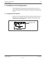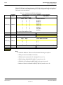
1
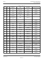
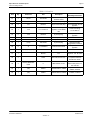
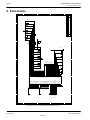
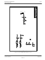
S1D13706 Embedded Memory LCD Controller
S5U13706P00C100 Evaluation Board
User Manual
Document Number: X31B-G-021-01
Status: Revision 1.1
Issue Date: 2009/03/03
© SEIKO EPSON CORPORATION 2007 - 2009. All Rights Reserved.
Information in this document is subject to change without notice. You may download and use this document, but only for your own use in
evaluating Seiko Epson/EPSON products. You may not modify the document. Epson Research and Development, Inc. disclaims any
representation that the contents of this document are accurate or current. The Programs/Technologies described in this document may contain
material protected under U.S. and/or International Patent laws.
EPSON is a registered trademark of Seiko Epson Corporation. All other Trademarks are the property of their respective owners
Revision 1.1
Page 2
Epson Research and Development
Vancouver Design Center
S1D13706
X31B-G-021-01
S5U13706P00C100 Evaluation Board User Manual
Issue Date: 2009/03/03
Revision 1.1
Epson Research and Development
Vancouver Design Center
Page 3
Table of Contents
1
Introduction . . . . . . . . . . . . . . . . . . . . . . . . . . . . . . . . . . . . . . . . 5
2
Features . . . . . . . . . . . . . . . . . . . . . . . . . . . . . . . . . . . . . . . . . . 6
3
Installation and Configuration . . . . . . . . . . . . . . . . . . . . . . . . . . . . . . 7
3.1 Configuration DIP Switches . . . . . . . . . . . . . . . . . . . . . . . . . . 7
3.2 Configuration Jumpers . . . . . . . . . . . . . . . . . . . . . . . . . . . . 9
4
CPU Interface . . . . . . . . . . . . . . . . . . . . . . . . . . . . . . . . . . . . . . 11
4.1 CPU Interface Pin Mapping . . . . . . . . . . . . . . . . . . . . . . . . . 11
4.2 CPU Bus Connector Pin Mapping . . . . . . . . . . . . . . . . . . . . . . 12
5
LCD Interface Pin Mapping
6
Technical Description . . . . . . . . . . . . . . . . . . . . . . . . .
6.1 PCI Bus Support . . . . . . . . . . . . . . . . . . . . . .
6.2 Direct Host Bus Interface Support . . . . . . . . . . . . . . .
6.3 S1D13706 Embedded Memory . . . . . . . . . . . . . . . . .
6.4 Software Adjustable LCD Backlight Intensity Support Using PWM . .
6.5 Passive/Active LCD Panel Support . . . . . . . . . . . . . . .
6.5.1 Buffered LCD Connector . . . . . . . . . . . . . . . . . . . . . .
6.5.2 Extended LCD Connector . . . . . . . . . . . . . . . . . . . . . .
6.6 External oscillator support for CLKI and CLKI2 . . . . . . . . . .
7
References . . . . . . . . . . . . . . . . . . . . . . . . . . . . . . . . . . . . . . . 18
7.1 Documents . . . . . . . . . . . . . . . . . . . . . . . . . . . . . . . 18
7.2 Document Sources . . . . . . . . . . . . . . . . . . . . . . . . . . . . 18
8
Parts List . . . . . . . . . . . . . . . . . . . . . . . . . . . . . . . . . . . . . . . . 19
9
Schematics . . . . . . . . . . . . . . . . . . . . . . . . . . . . . . . . . . . . . . . 22
. . . . . . . . . . . . . . . . . . . . . . . . . . . . . . 14
.
.
.
.
.
.
.
.
.
. . . . . . .
. . . . . .
. . . . . .
. . . . . .
. . . . . .
. . . . . .
. . . . . . . .
. . . . . . . .
. . . . . .
16
16
16
16
16
17
17
17
17
10 Board Layout . . . . . . . . . . . . . . . . . . . . . . . . . . . . . . . . . . . . . . 27
11 Technical Support . . . . . . . . . . . . . . . . . . . . . . . . . . . . . . . . . . . 28
11.1 EPSON LCD Controllers (S1D13706) . . . . . . . . . . . . . . . . . . . . . 28
S5U13706P00C100 Evaluation Board User Manual
Issue Date: 2009/03/03
S1D13706
X31B-G-021-01
Revision 1.1
Page 4
Epson Research and Development
Vancouver Design Center
S1D13706
X31B-G-021-01
S5U13706P00C100 Evaluation Board User Manual
Issue Date: 2009/03/03
Revision 1.1
Epson Research and Development
Vancouver Design Center
Page 5
1 Introduction
This manual describes the setup and operation of the S5U13706P00C100 Evaluation
Board. The board is designed as an evaluation platform for the S1D13706 Embedded
Memory LCD Controller.
This user manual is updated as appropriate. Please check the Epson Research and Development website at www.erd.epson.com for the latest revision of this document before
beginning any development.
We appreciate your comments on our documentation. Please contact us via email at
[email protected].
S5U13706P00C100 Evaluation Board User Manual
Issue Date: 2009/03/03
S1D13706
X31B-G-021-01
Revision 1.1
Page 6
Epson Research and Development
Vancouver Design Center
2 Features
Following are some features of the S5U13706P00C100 Evaluation Board:
• 100-pin TQFP S1D13706F00A Embedded Memory LCD Controller with 80K bytes of
embedded SRAM.
• Headers for connecting to various Host Bus Interfaces.
• Configuration options.
• Software adjustable backlight intensity support.
• 4/8-bit 3.3V or 5V single monochrome passive LCD panel support.
• 4/8/16-bit 3.3V or 5V single color passive LCD panel support.
• 9/12/18-bit 3.3V or 5V active matrix TFT LCD panel support.
• Direct interface for 18-bit Epson D-TFD LCD panel support.
• Direct interface for 18-bit Sharp HR-TFT LCD panel support.
• Software initiated power save mode.
• Hardware or software Video Invert support.
• External oscillator for CLKI and CLKI2.
S1D13706
X31B-G-021-01
S5U13706P00C100 Evaluation Board User Manual
Issue Date: 2009/03/03
Revision 1.1
Epson Research and Development
Vancouver Design Center
Page 7
3 Installation and Configuration
The S5U13706P00C100 is designed to support as many platforms as possible. The
S5U13706P00C100 incorporates a DIP switch and three jumpers which allow both the
evaluation board and S1D13706 LCD controller to be configured for a specified evaluation
platform.
3.1 Configuration DIP Switches
The S1D13706 has configuration inputs (CNF[7:0]) which are read on the rising edge of
RESET#. In order to configure the S1D13706 for multiple Host Bus Interfaces a tenposition DIP switch (S1) is provided. The following figure shows the location of DIP
switch SW1 on the S5U13706P00C100.
DIP Switch - SW1
Figure 3-1: Configuration DIP Switch (SW1) Location
S5U13706P00C100 Evaluation Board User Manual
Issue Date: 2009/03/03
S1D13706
X31B-G-021-01
Revision 1.1
Page 8
Epson Research and Development
Vancouver Design Center
The S1D13706 has 8 configuration inputs (CNF[7:0]) which are read on the rising edge of
RESET#. All S1D13706 configuration inputs are fully configurable using a ten position
DIP switch as described below.
Table 3-1: Configuration DIP Switch Settings
Switch
S1D13706
Signal
SW1-[3:1]
CNF[2:0]
SW1-4
SW1-5
SW1-6
CNF3
CNF4
CNF5
SW1-[8:7]
CNF[7:6]
SW1-91
SW1-10
-
Value on this pin at rising edge of RESET# is used to configure:
Closed (On/1)
Open (Off/0)
Select host bus interface as follows:
CNF2 CNF1 CNF0
Host Bus Interface
0
0
0
SH-4/SH-3
0
0
1
MC68K #1
0
1
0
MC68K #2
0
1
1
Generic #1
1
0
0
Generic #2
1
0
1
RedCap 2
1
1
0
DragonBall
1
1
1
Reserved
Note: The host bus interface is 16-bit.
Enable GPIO pins
Enable additional pins for D-TFD/HR-TFT
Big Endian bus interface
Little Endian bus interface
WAIT# is active high
WAIT# is active low
CLKI to BClk divide select:
CNF7 CNF6
CLKI to BClk Divide Ratio
0
0
1:1
0
1
2:1
1
0
3:1
1
1
4:1
Hardware Video Invert - invert video data1
Hardware Video Invert - normal video data1
Disable FPGA for non-PCI host
Enable FPGA for PCI host
= Required settings when used with PCI Bridge FPGA
Note
1
To enable the Hardware Video Invert function the following are required:
• GPIO pins must be enabled (S1-4 closed).
• GPIO0 must be connected to S1-9 (Jumper JP1 set to 1-2).
• GPIO Pin Input Enable (REG[A9h] bit 7) must be set to 1b.
• GPIO0 Pin IO Configuration (REG[A8h] bit 0) must be set to 0b.
• Hardware Video Invert Enable bit (REG[70h] bit 5) must be set to 1b.
S1D13706
X31B-G-021-01
S5U13706P00C100 Evaluation Board User Manual
Issue Date: 2009/03/03
Revision 1.1
Epson Research and Development
Vancouver Design Center
Page 9
3.2 Configuration Jumpers
The S5U13706P00C100 has seven jumper blocks which configure various setting on the
evaluation board. The jumper positions for each function are shown below.
Table 3-2: Jumper Summary
Jumper
Function
Position 1-2
Position 2-3
JP1
GPIO0 Connection
GPIO0 connected to
SW1-9 for hardware video
invert
—
JP4
JP6
GP0 Polarity on H1
LCD Panel Voltage
Normal (Active High)
+5V LCDVCC
Inverted (Active Low)
+3.3V LCDVCC
No Jumper
GPIO0 disconnected from
SW1-9 for direct
HR-TFT/D-TFD or GPIO
testing
—
—
= recommended settings
JP1 - GPIO0 Connection
JP1 selects whether GPIO0 is connected to SW1-9. SW1-9 is used to enable hardware video
invert on the S1D13706.
When the jumper is on (position 1-2), SW1-9 controls the hardware video invert feature
(default setting).
When the jumper is off, the hardware video invert feature is disabled. This setting must be
used for HR-TFT and D-TFD panels as GPIO0 is required for both panels. For details, refer
to the S1D13706 Hardware Functional Specification, document number X31B-A-001-xx.
Note
When configured for Sharp HR-TFT or Epson D-TFD panels, JP1 must be set to no
jumper and JP6 must be set to position 2-3.
JP1
GPIO0 connected GPIO0 disconnected
to SW1-9
from SW1-9
Figure 3-2: Configuration Jumper (JP1) Location
S5U13706P00C100 Evaluation Board User Manual
Issue Date: 2009/03/03
S1D13706
X31B-G-021-01
Revision 1.1
Page 10
Epson Research and Development
Vancouver Design Center
JP4 - GPO Polarity on H1
JP4 selects the polarity of the GPO signal available on LCD Connector H1.
Position 1-2 sends the GPO signal directly to H1 (default setting).
Position 2-3 inverts the GPO signal before sending it to H1.
JP4
Normal
Inverted
Figure 3-3: Configuration Jumper (JP4) Location
JP6 - LCD Panel Voltage
JP6 selects the voltage level to the LCD panel.
Position 1-2 sets the voltage level to 5.0V.
Position 2-3 sets the voltage level to 3.3V (default setting).
Note
When configured for Sharp HR-TFT or Epson D-TFD panels, JP1 must be set to no
jumper and JP6 must be set to position 2-3.
JP6
5.0V
3.3V
Figure 3-4: Configuration Jumper (JP6) Location
S1D13706
X31B-G-021-01
S5U13706P00C100 Evaluation Board User Manual
Issue Date: 2009/03/03
Revision 1.1
Epson Research and Development
Vancouver Design Center
Page 11
4 CPU Interface
4.1 CPU Interface Pin Mapping
Table 4-1: CPU Interface Pin Mapping
Generic #2
Hitachi
SH-3 /SH-4
Motorola
MC68K #1
Motorola
MC68K #2
Motorola
REDCAP2
Motorola
MC68EZ328/
MC68VZ328
DragonBall
A[16:1]
A[16:1]
A[16:1]
A[16:1]
A[16:1]
A[16:1]
A[16:1]
A01
A0
A01
LDS#
A0
A01
A01
D[15:0]
D[15:0]
D[15:0]
D[15:0]
D[15:0]2
D[15:0]
D[15:0]
CSn#
CSA#
CLK
S1D13706
Pin Name
Generic #1
AB[16:1]
AB0
DB[15:0]
CS#
External Decode
CSn#
M/R#
CLKI
BS#
External Decode
External Decode
BUSCLK
BUSCLK
Connected to
VDD3
CKIO
CLK
CLK
CLK
BS#
AS#
AS#
Connected to VDD3
RD/WR#
RD1#
Connected to
VDD3
RD/WR#
R/W#
R/W#
R/W#
Connected to
VDD3
RD#
RD0#
RD#
RD#
Connected to
VDD3
SIZ1
OE#
OE#
WE0#
WE0#
WE#
WE0#
Connected to
VDD3
SIZ0
EB1#
LWE#
WE1#
WE1#
BHE#
WE1#
UDS#
DS#
EB0#
UWE#
DTACK#
DSACK1#
N/A
DTACK#
RESET#
RESET#
RESET#
RESET#
WAIT#
WAIT#
WAIT#
WAIT#/
RDY#
RESET#
RESET#
RESET#
RESET#
Note
1
2
3
A0 for these busses is not used internally by the S1D13706.
If the target MC68K bus is 32-bit, then these signals should be connected to D[31:16].
These pins are not used in their corresponding Host Bus Interface mode. Systems are
responsible for externally connecting them to the host interface IO VDD.
S5U13706P00C100 Evaluation Board User Manual
Issue Date: 2009/03/03
S1D13706
X31B-G-021-01
Revision 1.1
Page 12
Epson Research and Development
Vancouver Design Center
4.2 CPU Bus Connector Pin Mapping
Table 4-2: CPU Bus Connector (H3) Pinout
Connector
Pin No.
Comments
1
Connected to DB0 of the S1D13706
2
Connected to DB1 of the S1D13706
3
Connected to DB2 of the S1D13706
4
Connected to DB3 of the S1D13706
5
Ground
6
Ground
7
Connected to DB4 of the S1D13706
8
Connected to DB5 of the S1D13706
9
Connected to DB6 of the S1D13706
10
Connected to DB7 of the S1D13706
11
Ground
12
Ground
13
Connected to DB8 of the S1D13706
14
Connected to DB9 of the S1D13706
15
Connected to DB10 of the S1D13706
16
Connected to DB11 of the S1D13706
17
Ground
18
Ground
19
Connected to DB12 of the S1D13706
20
Connected to DB13 of the S1D13706
21
Connected to DB14 of the S1D13706
22
Connected to DB15 of the S1D13706
23
Connected to RESET# of the S1D13706
24
Ground
25
Ground
26
Ground
27
+12 volt supply
28
+12 volt supply
29
Connected to WE0# of the S1D13706
30
Connected to WAIT# of the S1D13706
31
Connected to CS# of the S1D13706
32
Connected to MR# of the S1D13706
33
Connected to WE1# of the S1D13706
34
Connected to TXVDD1
S1D13706
X31B-G-021-01
S5U13706P00C100 Evaluation Board User Manual
Issue Date: 2009/03/03
Revision 1.1
Epson Research and Development
Vancouver Design Center
Page 13
Table 4-3: CPU Bus Connector (H4) Pinout
Connector
Pin No.
Comments
1
Connected to A0 of the S1D13706
2
Connected to A1 of the S1D13706
3
Connected to A2 of the S1D13706
4
Connected to A3 of the S1D13706
5
Connected to A4 of the S1D13706
6
Connected to A5 of the S1D13706
7
Connected to A6 of the S1D13706
8
Connected to A7 of the S1D13706
9
Ground
10
Ground
11
Connected to A8 of the S1D13706
12
Connected to A9 of the S1D13706
13
Connected to A10 of the S1D13706
14
Connected to A11 of the S1D13706
15
Connected to A12 of the S1D13706
16
Connected to A13 of the S1D13706
17
Ground
18
Ground
19
Connected to A14 of the S1D13706
20
Connected to A15 of the S1D13706
21
Connected to A16 of the S1D13706
22
Not connected
23
Not connected
24
Not connected
25
Ground
26
Ground
27
+5 volt supply
28
+5 volt supply
29
Connected to RD/WR# of the S1D13706
30
Connected to BS# of the S1D13706
31
Connected to BUSCLK of the S1D13706
32
Connected to RD# of the S1D13706
33
Not connected
34
Not connected
S5U13706P00C100 Evaluation Board User Manual
Issue Date: 2009/03/03
S1D13706
X31B-G-021-01
Revision 1.1
Page 14
Epson Research and Development
Vancouver Design Center
5 LCD Interface Pin Mapping
Table 5-1: LCD Signal Connector (H1)
Monochrome
Passive
Color Passive Panel
Color TFT Panel
Pin
Name
Connector
Pin No.
4-bit
8-bit
4-bit
8-bit
8-bit
16-Bit
9-bit
12-bit
FPDAT0
1
driven 0
D0
driven 0
D0 (B5)1
D0 (G3)1
D0 (R6)1
R2
R3
FPDAT1
3
driven 0
D1
driven 0
D1 (R5)1
D1 (R3)1
D1 (G5)1
R1
FPDAT2
5
driven 0
D2
driven 0
D2 (G4)1
D2 (B2)1
D2 (B4)1
FPDAT3
7
driven 0
D3
driven 0
D3 (B3)1
D3 (G2)1
FPDAT4
9
D0
D4
D0 (R2)1
D4 (R3)1
(B1)1
1
Single
Single
Sharp
HR-TFT1
Epson
D-TFD1
18-bit
18-bit
18-bit
R5
R5
R5
R2
R4
R4
R4
R0
R1
R3
R3
R3
D3 (R4)1
G2
G3
G5
G5
G5
D4 (R2)1
D8 (B5)1
1
Others
Format 1 Format 2
G1
G2
G4
G4
G4
D5 (G2)
D5 (B1)
D9 (R5)1
G0
G1
G3
G3
G3
D2 (G1)1
D6 (B1)1
D6 (G1)1
D10 (G4)1
B2
B3
B5
B5
B5
D7
D3 (R1)1
D7 (R1)1
D7 (R1)1
D11 (B3)1
B1
B2
B4
B4
B4
driven 0
driven 0
driven 0
driven 0
driven 0
D4 (G3)1
B0
B1
B3
B3
B3
19
driven 0
driven 0
driven 0
driven 0
driven 0
D5 (B2)1
driven 0
R0
R2
R2
R2
FPDAT10
21
driven 0
driven 0
driven 0
driven 0
driven 0
D6 (R2)1
driven 0
driven 0
R1
R1
R1
FPDAT11
23
driven 0
driven 0
driven 0
driven 0
driven 0
D7 (G1)1
driven 0
driven 0
R0
R0
R0
FPDAT12
25
driven 0
driven 0
driven 0
driven 0
driven 0
D12 (R3)1
driven 0
G0
G2
G2
G2
FPDAT13
27
driven 0
driven 0
driven 0
driven 0
driven 0
D13 (G2)1
driven 0
driven 0
G1
G1
G1
FPDAT14
29
driven 0
driven 0
driven 0
driven 0
driven 0
D14 (B1)1
driven 0
driven 0
G0
G0
G0
FPDAT15
31
driven 0
driven 0
driven 0
driven 0
driven 0
D15 (R1)1
driven 0
B0
B2
B2
B2
FPDAT16
4
driven 0
driven 0
driven 0
driven 0
driven 0
driven 0
driven 0
driven 0
B1
B1
B1
FPDAT17
6
driven 0
driven 0
driven 0
driven 0
driven 0
driven 0
driven 0
driven 0
B0
B0
B0
FPSHIFT
33
CLK
XSCL
DRDY
35 & 38
no
connect
GCP
FPDAT5
11
D1
D5
D1
FPDAT6
13
D2
D6
FPDAT7
15
D3
FPDAT8
17
FPDAT9
FPSHIFT
MOD
FPSHIFT2
MOD
DRDY
FPLINE
37
FPLINE
LP
LP
FPFRAME
39
FPFRAME
SPS
DY
GND
2, 8, 14, 20,
26
PWMOUT
28
PWMOUT
NC
30
Not connected
LCDVCC (3.3V / 5.0V)
MOD3
GPO2
GND
VCC
32
+12V
34
+12V
NC
36
Not connected
GPO
40
GPO2 (for controlling on-board LCD bias power supply on/off)
Note
1These
pin mappings use signal names commonly used for each panel type, however
signal names may differ between panel manufacturers. The values shown in brackets
represent the color components as mapped to the corresponding FPDATxx signals at
the first valid edge of FPSHIFT. For further FPDATxx to LCD interface mapping, see
the S1D13706 Hardware Functional Specification, document number
X31B-A-001-xx.
2GPO on H1 can be inverted by setting JP4 to 2-3.
3
The Sharp HR-TFT MOD signal controls the panel power. This must not be confused
with the MOD signal used on many passive panels.
S1D13706
X31B-G-021-01
S5U13706P00C100 Evaluation Board User Manual
Issue Date: 2009/03/03
Revision 1.1
Epson Research and Development
Vancouver Design Center
Page 15
Table 5-2: Extended LCD Signal Connector (H2)
Monochrome
Passive Panel
Color Passive Panel
Color TFT Panel
Pin
Name
Connector
Pin No.
GPIO0
1
GPIO0
PS
XINH
GPIO1
3
GPIO1
CLS
YSCL
GPIO2
5
GPIO2
REV
FR
GPIO3
7
GPIO3
SPL
FRS
GPIO4
9
GPIO4
GPIO4
RES
GPIO5
11
GPIO5
GPIO5
DD_P1
GPIO6
GPIO6
YSCLD
Single
Single
4-bit
8-bit
Others
Format 1 Format 2
4-bit
8-bit
8-bit
16-Bit
GPIO6
13
CVOUT
15
CVOUT
GND
2, 4, 6, 8, 10,
12, 14, 16
GND
9-bit
12-bit
18-bit
HR-TFT1
D-TFD1
18-bit
18-bit
Note
1
When dip switch SW1-4 is open (CNF3 = 0 at RESET#), GPIO[6:0] are at low output
states after reset. If REG[10h] bits 1-0 are set for either HR-TFT or D-TFD, some
of the pins are used for the HR-TFT or D-TFD interfaces and are not available as
GPIO pins.
S5U13706P00C100 Evaluation Board User Manual
Issue Date: 2009/03/03
S1D13706
X31B-G-021-01
Revision 1.1
Page 16
Epson Research and Development
Vancouver Design Center
6 Technical Description
6.1 PCI Bus Support
The S1D13706 does not have on-chip PCI bus interface support. The S1D13706P00C100
uses the PCI Bridge FPGA to support the PCI bus.
6.2 Direct Host Bus Interface Support
The S5U13706P00C100 is specifically designed to work using the PCI Bridge FPGA in a
standard PCI bus environment. However, the S1D13706 directly supports many other host
bus interfaces. Connectors H3 and H4 provide the necessary IO pins to interface to these
host buses. For further information on the host bus interfaces supported, see “CPU
Interface” on page 11.
Note
The PCI Bridge FPGA must be disabled using SW1-10 in order for direct host bus interfaces to operate properly.
6.3 S1D13706 Embedded Memory
The S1D13706 has 80K bytes of embedded SRAM. The 80K byte display buffer address
space is directly and contiguously available through the 17-bit address bus.
6.4 Software Adjustable LCD Backlight Intensity Support Using PWM
The S1D13706 provides Pulse Width Modulation output on PWMOUT. PWMOUT can be
used to control LCD panels which support PWM control of the backlight inverter. The
PWMOUT signal is provided on the buffered LCD connector (H1).
S1D13706
X31B-G-021-01
S5U13706P00C100 Evaluation Board User Manual
Issue Date: 2009/03/03
Revision 1.1
Epson Research and Development
Vancouver Design Center
Page 17
6.5 Passive/Active LCD Panel Support
The S1D13706 directly supports:
• 4/8-bit single monochrome passive panels.
• 4/8/16-bit single color passive panels.
• 9/12/18-bit TFT active matrix panels.
• 18-bit Sharp HR-TFT panels.
• 18-bit Epson D-TFD panels.
All the necessary signals are provided on the 40-pin LCD connector, H1, and 16-pin
Extended LCD Connector, H2. For connection information, see Section 5, “LCD Interface
Pin Mapping” on page 14.
The S5U13706P00C100 does not provide a power supply for the LCD bias voltage needed
by passive LCD panels. An external power supply is required to provide the bias LCD
voltage to the LCD panel.
6.5.1 Buffered LCD Connector
The buffered LCD connector (H1) provides the same LCD panel signals as those directly
from S1D13706, but with voltage-adapting buffers selectable to 3.3V or 5.0V. Pin 32 on
this connector provides a voltage level of 3.3V or 5.0V to the LCD panel logic (see “JP6 LCD Panel Voltage” on page 10 for information on setting the panel voltage).
6.5.2 Extended LCD Connector
The S1D13706 directly supports Sharp 18-bit HR-TFT and Epson 18-bit D-TFD panels.
The extended LCD connector (H2) provides the extra signals required to support these
panels. The signals on this connector are also buffered from the S1D13706 and adjustable
to 3.3V or 5.0V (see “JP6 - LCD Panel Voltage” on page 10 for details on setting the panel
voltage).
6.6 External oscillator support for CLKI and CLKI2
The S1D13706 uses CLKI and CLKI2 signals provided by two +5V oscillators. The oscillators are mounted on the evaluation board in 14-pin DIP sockets. The 5V clock signals are
shifted to 3.3V which is accepted by the S1D13706.
S5U13706P00C100 Evaluation Board User Manual
Issue Date: 2009/03/03
S1D13706
X31B-G-021-01
Revision 1.1
Page 18
Epson Research and Development
Vancouver Design Center
7 References
7.1 Documents
• Epson Research and Development, Inc., S1D13706 Hardware Functional Specification,
document number X31B-A-001-xx.
• Epson Research and Development, Inc., S1D13706 Programming Notes and Examples,
document number X31B-G-003-xx.
7.2 Document Sources
• Epson Research and Development: http://www.erd.epson.com.
S1D13706
X31B-G-021-01
S5U13706P00C100 Evaluation Board User Manual
Issue Date: 2009/03/03
Revision 1.1
Epson Research and Development
Vancouver Design Center
Page 19
8 Parts List
Table 8-1: Parts List
Part
Description
Manufacturer / Part No. /
Assembly Instructions
16
C1, C2, C3, C4, C5, C6,
C7, C8, C9, C10, C11,
C13, C16, C17, C18,
C19, C20, C21, C25,
C27, C29
0.1u
50V X7R +/-5%, 1206
pckg.
Panasonic-ECG ECJ3VB1H104K. Do not
populate C9, C10, C11,
C25, C27
2
0
C26, C12
10u 10V
10u 10V
Do not purchase. Do not
populate.
3
0
C15, C14
n/p
1206 pckg.
Do not purchase. Do not
populate.
4
0
C22, C28
22u 10V
Tantalum C-Size, 10V +/10%
Do not purchase. Do not
populate.
5
9
C23, C38, C39, C40,
C41, C42, C43, C44,
C45, C46
0.22uF
Ceramic Chip 0.22uF,
50V, X7R +/-5%, 1206
pckg
Kemet C1206C224J5RAC
or equivalent capacitor
6
0
C24, C32
10u 63V
Electrolytic, Radial Lead
63V +/-20%
Do not purchase. Do not
populate.
7
4
C30, C34, C35, C37
68u 10V
Tantalum D-Size,
68uF,10V, +/-10%
Kemet T491D686K010AS
(altern -Panasonic
ECST1AD686R (Digikey).
8
0
C31
1n
50V X7R +/-5%, 1206
pckg
Do not purchase. Do not
populate.
9
2
C36, C33
33u 20V
Tantalum D-Size,
33uF,20V, +/-10%
Kemet T491D336K020AS
(altern -Panasonic
ECST1AD336R (Digikey)
10
0
D2, D1
1N5819
Schottky Barrier Rectifier,
MELF pckg.
Do not purchase. Do not
populate.
11
1
H1
HEADER 20X2
20x2, shrouded header,
keyed, straight
Samtec TST-120-01-G-D
12
1
H2
HEADER 8X2
8x2, shrouded header,
keyed, straight
Samtec TST-108-01-G-D
13
2
H4, H3
HEADER 17X2
14
1
JP7, JP1
HEADER 2
2x1 .1” pitch unshrouded
header
15
2
JP2, JP3, JP4, JP5,
JP6
HEADER 3
3x1 .1” pitch unshrouded Do not populate JP2, JP3,
header
JP5
16
0
L2, L1
47uH
Shielded SMT power
inductor, +/-20%, 1.17A,
0.18 ohm
Do not purchase. Do not
populate.
17
0
Q1
MMBT3906
PNP Transistor / SOT-23
Do not purchase. Do not
populate.
Item
Qty
Reference
1
S5U13706P00C100 Evaluation Board User Manual
Issue Date: 2009/03/03
17x2, 0.1” pitch, .025” sq.
Samtec TSW-117-05-G-D
unshrouded header
Do not populate JP7
S1D13706
X31B-G-021-01
Revision 1.1
Page 20
Epson Research and Development
Vancouver Design Center
Table 8-1: Parts List
Item
Qty
Reference
Part
Description
Manufacturer / Part No. /
Assembly Instructions
18
0
Q2
MMFT3055VL
N-channel FET, SOT-223
pckg.
Do not purchase. Do not
populate.
19
0
Q3
FZT792A
High gain transistor, SOT223 pckg.
Do not purchase. Do not
populate.
20
0
Q4, Q5
MMBT2222A
NPN transistor, SOT-23
pckg.
Do not purchase. Do not
populate.
21
14
R1-R9, R33, R36, R37,
R38, R39
15K
1206 / 5%
22
9
R10, R11, R12, R13,
R14, R15, R16, R17,
R18
330K
1206 / 5%
23
0
R19
12.4K 1%
1206 / 1%, E-96 series
Do not purchase. Do not
populate.
24
0
R20, R21
80K
1206 / 5%
Do not purchase. Do not
populate.
25
0
R22
402 1%
1206 / 1%, E-96 series
Do not purchase. Do not
populate.
26
0
R23
301 1%
1206 / 1%, E-96 series
Do not purchase. Do not
populate.
27
0
R24
200 POT
Trim POT
Do not purchase. Do not
populate.
28
0
R25
0.22 1/4W
1210 / 5% / 1/4W
Do not purchase. Do not
populate.
29
0
R26
470
1206 / 5%
Do not purchase. Do not
populate.
30
0
R27
22K
1206 / 5%
Do not purchase. Do not
populate.
31
1
R28, R29, R32
100K
1206 / 5%
Do not populate R28, R29
32
0
R30
1.2M
1206 / 5%
Do not purchase. Do not
populate.
33
0
R31
500K POT
Trim POT
Do not purchase. Do not
populate.
34
3
R34, R35, R40, R41
1K
1206 / 5%
Do not populate R41
35
1
SW1
SW DIP-10
Dip Switch 10-Position
Grayhill 76SB10ST
(Digikey GH1117-ND)
36
0
S1
SW DIP-4
DIP switch, 4-position
Do not purchase. Do not
populate.
37
1
U1
S1D13706F00A
100-pin TQFP15 surface
mount package
38
0
U2
LT1117CST-5
5V fixed voltage regulator,
SOT-223
Do not purchase. Do not
populate.
39
1
U3
74AHC04
SO-14 package
TI 74AHC04, SO-14
package
40
0
U4
ICD2061A
Wide SO-16 package
Do not purchase. Do not
populate.
S1D13706
X31B-G-021-01
S5U13706P00C100 Evaluation Board User Manual
Issue Date: 2009/03/03
Revision 1.1
Epson Research and Development
Vancouver Design Center
Page 21
Table 8-1: Parts List
Manufacturer / Part No. /
Assembly Instructions
Item
Qty
Reference
Part
Description
41
2
U6, U5
Test Socket
14 pin narrow DIP, screw
machine socket
42
4
U7, U8, U9, U10
74HCT244
Buffer, SO-20 package
TI74HCT244 or equivalent
43
0
U11
MAX754
16 pin narrow SO pckg.
Do not purchase. Do not
populate.
44
1
U12
LT1117CM-3.3
3.3V fixed voltage
regulator, 3 Lead Plastic
DD
Linear Technology
LT1117CM-3.3
45
0
U13
MAX749
8 pin SO pckg.
Do not purchase. Do not
populate.
46
1
U14
EPF6016TC144-2
144-pin QFP
Altera EPF6016TC144-2
47
1
U15
8-pin DIP socket
8-pin DIP socket
Machined socket, 8-pin
48
1
(U15)
EPC1PI8N
8-pin DIP pckg
Altera EPC1PI8N,
programmed, socketed
49
0
Y1
14.31818MHz
Vertical-mount HC-49
Do not purchase. Do not
populate.
50
3
(JP1), (JP4), (JP6)
Micro Shunt
51
1
Bracket
52
2
Screw
Pan head, #4-40 x 1/4”
Screw, pan head, #4-40 x
1/4”-please assemble
bracket onto board
53
2
Resistor SMD 0805
0ohm
0
0805 Resistor, 0 ohm
please mount on solder
side to short pins 2-3 of
JP2 and JP3
54
1
(U6)
50MHz
Oscillator DIP14, 50MHz
Epson SG8002DB,
50MHz, socketed
55
1
(U5)
6.5MHz
Oscillator DIP14, 6.5MHz
Epson SG8002DB,
6.5MHz, socketed
S5U13706P00C100 Evaluation Board User Manual
Issue Date: 2009/03/03
Computer Bracket, Blank Keystone - Cat. No. 9203
PCI
S1D13706
X31B-G-021-01
Revision 1.1
S1D13706
X31B-G-021-01
Revision 1.1
A
B
C
DB[15:0]
CLKI
CLKI2
CS#
M/R#
BS#
RD#
WE0#
WE1#
RD/WR#
RESET#
WAIT#
2,4,5
2
4,5
4,5
4,5
4,5
4,5
4,5
4,5
4,5
4,5
AB[16:0]
4,5
4,5
5
DB[15:0]
AB[16:0]
DB0
DB1
DB2
DB3
DB4
DB5
DB6
DB7
DB8
DB9
DB10
DB11
DB12
DB13
DB14
DB15
AB0
AB1
AB2
AB3
AB4
AB5
AB6
AB7
AB8
AB9
AB10
AB11
AB12
AB13
AB14
AB15
AB16
14
25
36
50
62
75
100
6
7
8
9
10
11
12
13
17
15
77
35
34
33
32
31
30
29
28
27
24
23
22
21
20
19
18
5
4
3
2
99
98
97
96
95
94
93
92
91
90
89
88
87
U1
VSS
VSS
VSS
VSS
VSS
VSS
VSS
CS#
M/R#
BS#
RD#
WE0#
WE1#
RD/WR#
RESET#
WAIT#
CLKI
CLKI2
DB0
DB1
DB2
DB3
DB4
DB5
DB6
DB7
DB8
DB9
DB10
DB11
DB12
DB13
DB14
DB15
AB0
AB1
AB2
AB3
AB4
AB5
AB6
AB7
AB8
AB9
AB10
AB11
AB12
AB13
AB14
AB15
AB16
4
S1D13706F00A
TESTEN
COREVDD
COREVDD
NIOVDD
NIOVDD
NIOVDD
NIOVDD
HIOVDD
HIOVDD
FPFRAME
FPLINE
FPSHIFT
DRDY
CVOUT
PW MOUT
GP0
GPIO0
GPIO1
GPIO2
GPIO3
GPIO4
GPIO5
GPIO6
FPDAT0
FPDAT1
FPDAT2
FPDAT3
FPDAT4
FPDAT5
FPDAT6
FPDAT7
FPDAT8
FPDAT9
FPDAT10
FPDAT11
FPDAT12
FPDAT13
FPDAT14
FPDAT15
FPDAT16
FPDAT17
CNF0
CNF1
CNF2
CNF3
CNF4
CNF5
CNF6
CNF7
4
86
1
51
37
49
63
76
16
26
52
53
54
48
46
38
47
45
44
43
42
41
40
39
55
56
57
58
59
60
61
64
65
66
67
68
69
70
71
72
73
74
85
84
83
82
81
80
79
78
FPDAT0
FPDAT1
FPDAT2
FPDAT3
FPDAT4
FPDAT5
FPDAT6
FPDAT7
FPDAT8
FPDAT9
FPDAT10
FPDAT11
FPDAT12
FPDAT13
FPDAT14
FPDAT15
FPDAT16
FPDAT17
C1
0.1u
C2
0.1u
R10
330K
3
3
3
3
3
3
3
3
3
3
3
3
3
3
3
R13
330K
C4
0.1u
FPDAT[17:0]
R12
330K
FPFRAME
FPLINE
FPSHIFT
DRDY
CVOUT
PWMOUT
GPO
GPIO0
GPIO1
GPIO2
GPIO3
GPIO4
GPIO5
GPIO6
C3
0.1u
R11
330K
3
3
C5
0.1u
R14
330K
C6
0.1u
R15
330K
R16
330K
C7
0.1u
+3.3V
R17
330K
C8
0.1u
R18
330K
1
2
3
4
5
6
7
8
9
10
SW DIP-10
SW1
20
19
18
17
16
15
14
13
12
11
2
2
15K
R1
GPIO0
HEADER 2
JP1
2
1
D
5
15K
R2
Date:
Size
B
Title
15K
R4
5
15K
R5
15K
R6
15K
R7
Monday, March 05, 2007
Document Number
<Doc>
15K
R8
1
Sheet
S5U13706P00C100 - S1D13706F00A/DIP SW
nCONFIG
15K
R3
+3.3V
1
1
15K
R9
of
5
Rev
A
B
C
D
Page 22
Epson Research and Development
Vancouver Design Center
9 Schematics
Figure 9-1: S5U13706P00C100 Schematics (1 of 5)
S5U13706P00C100 Evaluation Board User Manual
Issue Date: 2009/03/03
S5U13706P00C100 Evaluation Board User Manual
Issue Date: 2009/03/03
Revision 1.1
A
B
C
+5V
+5V
5
+3.3V
7
13
7
3
14
7
1
14
14
+3.3V
+3.3V
C17
0.1u
C16
0.1u
74AHC04
U3F
4
12
74AHC04
U3B
2
Test Socket
GND
VCC
U6
Test Socket
GND
VCC
U5
74AHC04
U3A
7
14
7
14
NC
OUT
NC
OUT
8
1
8
1
For U3
+3.3V
7
9
14
7
5
14
C13
0.1u
+3.3V
+3.3V
4
1,4,5
8
6
BUSCLK
74AHC04
U3D
74AHC04
U3C
4
CLKI
CLKI2
1,4,5
1
3
3
+5V
C29
0.1u
3
2
VIN
2
U12
LT1117CM-3.3
ADJ
1
D
5
VOUT
2
Date:
Size
B
Title
+
+3.3V
1 2
2 3
5.0V LCD Panels
3.3V LCD Panels
3
2
1
Monday, March 05, 2007
Document Number
<Doc>
1
Sheet
S5U13706P00C100 - Clocks and Power Supplies
C30
68u 10V
LCDVCC
+5V
JP6
HEADER 3
1
2
of
5
Rev
A
B
C
D
Epson Research and Development
Vancouver Design Center
Page 23
Figure 9-2: S5U13706P00C100 Schematics (2 of 5)
S1D13706
X31B-G-021-01
S1D13706
X31B-G-021-01
Revision 1.1
A
B
C
D
1
1
5
5
1
1
1
1
1
+3.3V
FPDAT[17:0]
FPSHIFT
DRDY
FPLINE
FPFRAME
PWMOUT
GPO
FPDAT[17:0]
7
11
14
74AHC04
U3E
10
JP4
1
2
3
HEADER 3
4
4
1
1
1
1
1
1
1
1
GPIO0
GPIO1
GPIO2
GPIO3
GPIO4
GPIO5
GPIO6
CVOUT
FPDAT16
FPDAT17
FPDAT8
FPDAT9
FPDAT10
FPDAT11
FPDAT12
FPDAT13
FPDAT14
FPDAT15
FPDAT0
FPDAT1
FPDAT2
FPDAT3
FPDAT4
FPDAT5
FPDAT6
FPDAT7
1
19
2
4
6
8
11
13
15
17
1
19
2
4
6
8
11
13
15
17
1
19
2
4
6
8
11
13
15
17
1
19
2
4
6
8
11
13
15
17
3
74HCT244
1G
2G
1A1
1A2
1A3
1A4
2A1
2A2
2A3
2A4
U10
74HCT244
1G
2G
1A1
1A2
1A3
1A4
2A1
2A2
2A3
2A4
U9
74HCT244
1G
2G
1A1
1A2
1A3
1A4
2A1
2A2
2A3
2A4
U8
74HCT244
1G
2G
1A1
1A2
1A3
1A4
2A1
2A2
2A3
2A4
U7
3
VCC
GND
1Y1
1Y2
1Y3
1Y4
2Y1
2Y2
2Y3
2Y4
VCC
GND
1Y1
1Y2
1Y3
1Y4
2Y1
2Y2
2Y3
2Y4
VCC
GND
1Y1
1Y2
1Y3
1Y4
2Y1
2Y2
2Y3
2Y4
VCC
GND
1Y1
1Y2
1Y3
1Y4
2Y1
2Y2
2Y3
2Y4
20
10
18
16
14
12
9
7
5
3
20
10
18
16
14
12
9
7
5
3
20
10
18
16
14
12
9
7
5
3
20
10
18
16
14
12
9
7
5
3
BFPDAT16
BFPDAT17
BFPDAT8
BFPDAT9
BFPDAT10
BFPDAT11
BFPDAT12
BFPDAT13
BFPDAT14
BFPDAT15
BFPDAT0
BFPDAT1
BFPDAT2
BFPDAT3
BFPDAT4
BFPDAT5
BFPDAT6
BFPDAT7
LCDVCC
C21
0.1u
LCDVCC
C20
0.1u
LCDVCC
C19
0.1u
LCDVCC
C18
0.1u
2
BFPDAT0
BFPDAT1
BFPDAT2
BFPDAT3
BFPDAT4
BFPDAT5
BFPDAT6
BFPDAT7
BFPDAT8
BFPDAT9
BFPDAT10
BFPDAT11
BFPDAT12
BFPDAT13
BFPDAT14
BFPDAT15
2
2
4
6
8
10
12
14
16
18
20
22
24
26
28
30
32
34
36
38
40
2
4
6
8
10
12
14
16
Date:
Size
B
Title
HEADER 8X2
1
3
5
7
9
11
13
15
H2
HEADER 20X2
1
3
5
7
9
11
13
15
17
19
21
23
25
27
29
31
33
35
37
39
H1
LCDVCC
+12V
Monday, March 05, 2007
Document Number
<Doc>
S5U13706P00C100 - LCD Connectors
BFPDAT16
BFPDAT17
BFPDAT[17:0]
1
Sheet
1
3
of
5
Rev
A
B
C
D
Page 24
Epson Research and Development
Vancouver Design Center
Figure 9-3: S5U13706P00C100 Schematics (3 of 5)
S5U13706P00C100 Evaluation Board User Manual
Issue Date: 2009/03/03
S5U13706P00C100 Evaluation Board User Manual
Issue Date: 2009/03/03
Revision 1.1
A
B
C
D
TRDY#
STOP#
PAR
5
5
5
C/BE0#
FRAME#
5
5
IDSEL
RST#
AD[31:0]
5
5
5
5
5
AD2
AD0
AD6
AD4
AD9
AD13
AD11
AD15
AD18
AD16
AD22
AD20
AD24
AD28
AD26
AD30
52
53
54
55
56
57
58
59
60
61
62
14
15
16
17
18
19
20
21
22
23
24
25
26
27
28
29
30
31
32
33
34
35
36
37
38
39
40
41
42
43
44
45
46
47
48
49
1
2
3
4
5
6
7
8
9
10
11
Place close to PCIB pin 5 & 6
68u 10V
+ C34
+5V
+5V +12V
PCI-A
C/BE0#
+3.3V
AD6
AD4
GND
AD2
AD0
+VI/O
REQ64#
+5V
+5V
68u 10V
+ C35
+5V
PCI-B
4
52
53
54
55
56
57
58
59
60
61
62
14
15
16
17
18
19
20
21
22
23
24
25
26
27
28
29
30
31
32
33
34
35
36
37
38
39
40
41
42
43
44
45
46
47
48
49
1
2
3
4
5
6
7
8
9
10
11
33u 20V
+ C36
+12V
+5V
Place close to PCIA pin 2
AD8
AD7
+3.3V
AD5
AD3
GND
AD1
+VI/O
ACK64#
+5V
+5V
RESERVED
GND
CLK
GND
REQ#
+VI/O
AD31
AD29
GND
AD27
AD25
+3.3V
C/BE3#
AD23
GND
AD21
AD19
+3.3V
AD17
C/BE2#
GND
IRDY#
+3.3V
DEVSEL#
GND
LOCK#
PERR#
+3.3V
SERR#
3.3V
C/BE1#
AD14
GND
AD12
AD10
GND
-12V
TCK
GND
TDO
+5V
+5V
INTB#
INTD#
PRSNT#1
RESERVED
PRSNT#2
PCIB1
Place close to PCIB pin 61 & 62
RESERVED
RST#
+VI/O
GNT#
GND
RESERVED
AD30
+3.3V
AD28
AD26
GND
AD24
IDSEL
+3.3V
AD22
AD20
GND
AD18
AD16
+3.3V
FRAME#
GND
TRDY#
GND
STOP#
+3.3V
SDONE
SBO#
GND
PAR
AD15
+3.3V
AD13
AD11
GND
AD9
TRST#
+12V
TMS
TDI
+5V
INTA#
INTC#
+5V
RESERVED
+VI/O
RESERVED
PCIA1
AD[31:0]
4
AD1
AD5
AD3
AD8
AD7
AD12
AD10
AD14
AD17
AD21
AD19
AD23
AD27
AD25
AD31
AD29
3
3
5
5
SERR#
C/BE1#
5
5
5
5
5
5
PERR#
DEVSEL#
IRDY#
C/BE2#
C/BE3#
CLK
1,5
1,5
1,5
1,2,5
1,5
1,5
1,5
1,5
RD/WR#
BUSCLK
AB[16:0]
WE0#
CS#
WE1#
RESET#
DB[15:0]
AB[16:0]
DB[15:0]
2
2
AB14
AB16
AB8
AB10
AB12
AB0
AB2
AB4
AB6
DB12
DB14
DB8
DB10
DB4
DB6
DB0
DB2
+5V
+12V
Date:
Size
B
Title
2
4
6
8
10
12
14
16
18
20
22
24
26
28
30
32
34
2
4
6
8
10
12
14
16
18
20
22
24
26
28
30
32
34
C33
33u 20V
C37
68u 10V
+5V
+12V
AB15
AB9
AB11
AB13
AB1
AB3
AB5
AB7
DB13
DB15
DB9
DB11
DB5
DB7
DB1
DB3
Monday, March 05, 2007
Document Number
<Doc>
1
Sheet
S5U13706P00C100 - Host Bus Connectors
+
+5V
HEADER 17X2
1
3
5
7
9
11
13
15
17
19
21
23
25
27
29
31
33
H4
+
+12V
HEADER 17X2
1
3
5
7
9
11
13
15
17
19
21
23
25
27
29
31
33
H3
1
4
BS#
RD#
WAIT#
M/R#
of
5
1,5
1,5
1,5
1,5
Rev
A
B
C
D
Epson Research and Development
Vancouver Design Center
Page 25
Figure 9-4: S5U13706P00C100 Schematics (4 of 5)
S1D13706
X31B-G-021-01
1
2
3
AD[31:0]
C/BE3#
IDSEL
C/BE2#
FRAME#
IRDY#
TRDY#
DEVSEL#
STOP#
PERR#
SERR#
PAR
C/BE1#
C/BE0#
4
4
4
4
4
4
4
4
4
4
4
4
4
RST#
4
4
CLK
4
A
AD28
AD27
AD26
AD31
AD30
AD29
AD[31:0]
1
2
3
4
5
6
7
8
9
10
11
12
13
14
15
16
17
18
19
20
21
22
23
24
25
26
27
28
29
30
31
32
33
34
35
36
IO1
IO2
IO3
nCE
GND
Vccint
Vccio
IO8
IO9
IO10
IO11
IO12
IO13
IO14
IO15
IO16
I17
GND
Vccio
I20
IO21
IO22
IO23
IO24
IO25
IO26
IO27
IO28
IO29
GND
Vccint
Vccio
MSEL
IO34
IO35
IO36
AD25
AD24
AB14
AB15
AB16
AB13
AB12
AB11
AB10
AB9
AB8
AB7
AB6
AB5
AB4
AB3
AB2
AB1
AB0
AD23
AD22
AD21
AD20
AD19
AD18
AD17
AD16
U14
B
nSTATUS
+5V
+3.3V
DATA
B
DB11
DB10
DB13
DB12
DB15
DB14
DCLK
144
143
142
141
140
139
138
137
136
135
134
133
132
131
130
129
128
127
126
125
124
123
122
121
120
119
118
117
116
115
114
113
112
111
110
109
DB[15:0]
AB[16:0]
C
108
107
106
105
104
103
102
101
100
99
98
97
96
95
94
93
92
91
90
89
88
87
86
85
84
83
82
81
80
79
78
77
76
75
74
73
C
AD5
AD6
AD7
AD0
AD1
AD2
AD3
AD4
DB0
DB2
DB1
DB6
DB5
DB4
DB3
DB9
DB8
DB7
CONF_DONE
EPF6016TC144-2
IO108
IO107
IO106
CONF_DONE
Vccio
Vccint
GND
IO101
IO100
IO99
IO98
IO97
IO96
IO95
IO94
IO93
I92
Vccio
GND
I89
IO88
IO87
IO86
IO85
IO84
IO83
IO82
IO81
IO80
IO79
Vccio
Vccint
GND
IO75
IO74
IO73
IO144
IO143
IO142
IO141
IO140
IO139
IO138
IO137
IO136
IO135
IO134
IO133
IO132
IO131
IO130
IO129
DCLK
Vccio
GND
DATA
IO124
IO123
IO122
IO121
IO120
IO119
IO118
IO117
IO116
IO115
IO114
IO113
IO112
IO111
IO110
IO109
IO37
IO38
IO39
IO40
IO41
IO42
IO43
IO44
IO45
IO46
IO47
IO48
IO49
IO50
IO51
IO52
nCONFIG
GND
Vccio
nSTATUS
IO57
IO58
IO59
IO60
IO61
IO62
IO63
IO64
IO65
IO66
IO67
IO68
IO69
IO70
IO71
IO72
AD15
AD14
AD13
AD12
AD11
AD10
AD9
Revision 1.1
37
38
39
40
41
42
43
44
45
46
47
48
49
50
51
52
53
54
55
56
57
58
59
60
61
62
63
64
65
66
67
68
69
70
71
72
S1D13706
X31B-G-021-01
AD8
4
A
+5V
R36
15K
R40
1K
R32
100K
R38
15K
nCONFIG
R37
15K
15K
R33
1
+3.3V
1,4
1,4
1,2,4
1,4
1,4
1,4
1,4
1,4
1,4
1,4
1,4
1,4
D
1
2
3
4
SW DIP-4
S1
8
7
6
5
+5V
Not Populated
DATA
DCLK
nSTATUS
CONF_DONE
R39
15K
DB[15:0]
AB[16:0]
BUSCLK
RD#
BS#
RD/WR#
WE1#
M/R#
CS#
WAIT#
WE0#
RESET#
D
1
2
3
4
U15
EPC1441PC8
DATA
VCC
VCC
DCLK
nCASC
OE
GND
nCS
0.22u
0.22u
Date:
Size
B
+3.3V
+5V
0.22u
C45
0.22u
C41
+3.3V
Monday, March 05, 2007
Document Number
<Doc>
E
Sheet
0.22u
C46
0.22u
C42
+5V
+5V
+5V
S5U13706P00C100 - FPGA--6016
C44
C43
0.22u
0.22u
+3.3V
+5V
C40
Title
8
7
6
5
FPGA configuration EPROM
R35
1K
C39
+5V
+5V
+5V
+5V
+5V
+3.3V
+5V
R34
1K
E
+5V
5
0.22u
C38
of
5
Rev
1
2
3
4
Page 26
Epson Research and Development
Vancouver Design Center
Figure 9-5: S5U13706P00C100 Schematics (5 of 5)
S5U13706P00C100 Evaluation Board User Manual
Issue Date: 2009/03/03
Epson Research and Development
Vancouver Design Center
Page 27
10 Board Layout
Figure 10-1: S5U13706P00C100 Board Layout
S5U13706P00C100 Evaluation Board User Manual
Issue Date: 2009/03/03
S1D13706
X31B-G-021-01
Revision 1.1
Page 28
Epson Research and Development
Vancouver Design Center
11 Technical Support
11.1 EPSON LCD Controllers (S1D13706)
AMERICA
ASIA
EPSON ELECTRONICS AMERICA, INC.
EPSON (CHINA) CO., LTD.
2580 Orchard Parkway
San Jose, CA 95131,USA
Phone: +1-800-228-3964
7F, Jinbao Bldg., No.89 Jinbao St.,
Dongcheng District,
Beijing 100005, CHINA
Phone: +86-10-6410-6655 FAX: +86-10-6410-7320
FAX: +1-408-922-0238
SHANGHAI BRANCH
7F, Block B, High-Tech Bldg., 900, Yishan Road,
Shanghai 200233, CHINA
Phone: +86-21-5423-5522 FAX: +86-21-5423-5512
EUROPE
EPSON EUROPE ELECTRONICS GmbH
Riesstrasse 15, 80992 Munich,
GERMANY
Phone: +49-89-14005-0
FAX: +49-89-14005-110
SHENZHEN BRANCH
12F, Dawning Mansion, Keji South 12th Road,
Hi-Tech Park, Shenzhen 518057, CHINA
Phone: +86-755-2699-3828 FAX: +86-755-2699-3838
EPSON HONG KONG LTD.
20/F, Harbour Centre, 25 Harbour Road
Wanchai, Hong Kong
Phone: +852-2585-4600
FAX: +852-2827-4346
Telex: 65542 EPSCO HX
EPSON TAIWAN TECHNOLOGY & TRADING LTD.
14F, No. 7, Song Ren Road,
Taipei 110, TAIWAN
Phone: +886-2-8786-6688 FAX: +886-2-8786-6660
EPSON SINGAPORE PTE., LTD.
1 HarbourFront Place,
#03-02 HarbourFront Tower One, Singapore 098633
Phone: +65-6586-5500
FAX: +65-6271-3182
SEIKO EPSON CORP.
KOREA OFFICE
50F, KLI 63 Bldg., 60 Yoido-dong
Youngdeungpo-Ku, Seoul, 150-763, KOREA
Phone: +82-2-784-6027
FAX: +82-2-767-3677
SEIKO EPSON CORP.
SEMICONDUCTOR OPERATIONS DIVISION
IC Sales Dept.
IC International Sales Group
421-8, Hino, Hino-shi, Tokyo 191-8501, JAPAN
Phone: +81-42-587-5814
FAX: +81-42-587-5117
S1D13706
X31B-G-021-01
S5U13706P00C100 Evaluation Board User Manual
Issue Date: 2009/03/03
Revision 1.1
Epson Research and Development
Vancouver Design Center
Page 29
Change Record
X31B-G-021-01
Revision 1.1 - Issued: March 03, 2009
• section 11 - update sales office addresses
X31B-G-021-01
Revision 1.0 - Issued: March 19, 2007
• initial draft
• minor edits
• added parts list
• added schematics
• updated tech support contact information
S5U13706P00C100 Evaluation Board User Manual
Issue Date: 2009/03/03
S1D13706
X31B-G-021-01
Revision 1.1