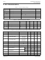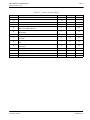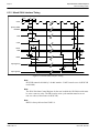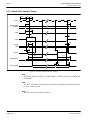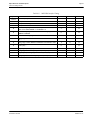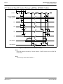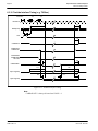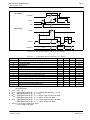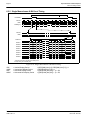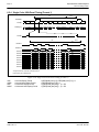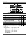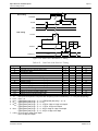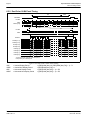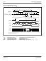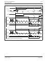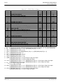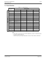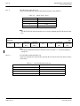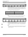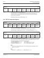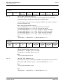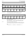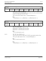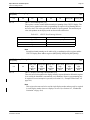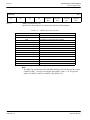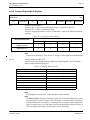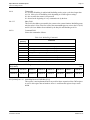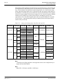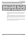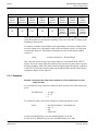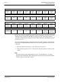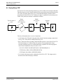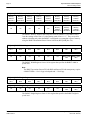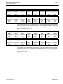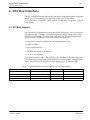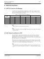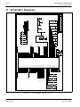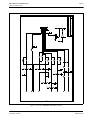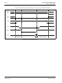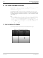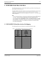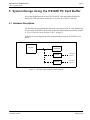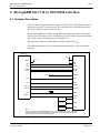
1
S1D13806 Embedded Memory Display Controller S1D13806 TECHNICAL MANUAL Document Number: X28B-Q-001-05 Copyright © 2001 Epson Research and Development, Inc. All Rights Reserved. Information in this document is subject to change without notice. You may download and use this document, but only for your own use in evaluating Seiko Epson/EPSON products. You may not modify the document. Epson Research and Development, Inc. disclaims any representation that the contents of this document are accurate or current. The Programs/Technologies described in this document may contain material protected under U.S. and/or International Patent laws. EPSON is a registered trademark of Seiko Epson Corporation. All other trademarks are the property of their respective owners. Page 2 Epson Research and Development Vancouver Design Center THIS PAGE LEFT BLANK S1D13806 X28B-Q-001-05 TECHNICAL MANUAL Issue Date: 01/04/17 Epson Research and Development Vancouver Design Center Page 3 COMPREHENSIVE SUPPORT TOOLS EPSON provides the designer and manufacturer a complete set of resources and tools for the development of LCD Graphics Systems. Documentation • Technical manuals • Evaluation/Demonstration board manual Evaluation/Demonstration Board • • • • • • • Assembled and fully tested Graphics Evaluation/Demonstration board Schematic of Evaluation/Demonstration board Parts List Installation Guide CPU Independent Software Utilities Evaluation Software Windows CE Display Driver Application Engineering Support EPSON offers the following services through their Sales and Marketing Network: • Sales Technical Support • Customer Training • Design Assistance Application Engineering Support Engineering and Sales Support is provided by: Japan Seiko Epson Corporation Electronic Devices Marketing Division 421-8, Hino, Hino-shi Tokyo 191-8501, Japan Tel: 042-587-5812 Fax: 042-587-5564 http://www.epson.co.jp Hong Kong Epson Hong Kong Ltd. 20/F., Harbour Centre 25 Harbour Road Wanchai, Hong Kong Tel: 2585-4600 Fax: 2827-4346 TECHNICAL MANUAL Issue Date: 01/04/17 North America Epson Electronics America, Inc. 150 River Oaks Parkway San Jose, CA 95134, USA Tel: (408) 922-0200 Fax: (408) 922-0238 http://www.eea.epson.com Taiwan Epson Taiwan Technology & Trading Ltd. 10F, No. 287 Nanking East Road Sec. 3, Taipei, Taiwan Tel: 02-2717-7360 Fax: 02-2712-9164 Europe Epson Europe Electronics GmbH Riesstrasse 15 80992 Munich, Germany Tel: 089-14005-0 Fax: 089-14005-110 Singapore Epson Singapore Pte., Ltd. No. 1 Temasek Avenue #36-00 Millenia Tower Singapore, 039192 Tel: 337-7911 Fax: 334-2716 S1D13806 X28B-Q-001-05 Page 4 Epson Research and Development Vancouver Design Center THIS PAGE LEFT BLANK S1D13806 X28B-Q-001-05 TECHNICAL MANUAL Issue Date: 01/04/17 ENERGY S AV I N G GRAPHICS EPSON S1D13806 S1D13806 Embedded Memory Display Controller March 2002 The S1D13806 is a highly integrated color LCD/CRT/TV graphics controller with embedded memory supporting a wide range of CPUs and display devices. The S1D13806 architecture is designed to meet the low cost, low power requirements of the embedded markets, such as Mobile Communications, Hand-Held PC’s, and Office Automation. The S1D13806 supports multiple CPUs, all LCD panel types, CRT, TV, and additionally provides a number of differentiating features. EPSON Independent Simultaneous Display technology allows the user to configure two different images on two different displays, while the SwivelView™, Hardware Cursor, Ink Layer, and BitBLT features offer substantial performance benefits. Products requiring digital camera input can take advantage of the directly supported WINNOV Videum® Cam digital interface. These features, combined with the S1D13806’s Operating System independence, make it an ideal display solution for a wide variety of applications. ■ FEATURES • SwivelView: 90°, 180°, 270° • 1280K bytes of embedded synchronous DRAM. • Multiple CPU interface support. • Resolutions up to: • • • 800x600 at a color depth of 16 bpp. 1024x768 at a color depth of 8 bpp. Display Support for: 4/8/16-bit passive panels. 9/12/18/2x9/2x12 TFT/D-TFD panels. CRT. NTSC and PAL TV Output. WINNOV Videum® Cam digital camera interface. • • • • • hardware rotation of displayed image. EPSON Independent Simultaneous Display: displays different images on different displays. Virtual Display Support Hardware Cursor or full screen Ink Layer. 2D BitBLT Engine. Software initiated Power Save Mode. Operating System Independent. ■ SYSTEM BLOCK DIAGRAM TV MediaPlug Interface or Analog Out CRT Control CPU Clock S1D13806 Digital Out FLAT PANEL X28B-C-001-09 1 GRAPHICS S1D13806 ■ DESCRIPTION Memory Interface • 1280K bytes of embedded synchronous DRAM. • Addressable as a single linear address space. CPU Interface • Supports the following interfaces: EPSON E0C33 NEC MIPS VR41xx Hitachi SH-4/SH-3 PC Card (PCMCIA) ISA bus Philips MIPS PR31500/PR31700 Motorola M68xxx StrongARM (PC Card) Motorola MPC8xx Toshiba MIPS TX39xx MPU with programmable READY • CPU Write buffer. Display Support • LCD Panels: 4/8/16-bit passive LCD interface. 9/12/18/2x9/2x12-bit TFT/D-TFD. • CRT: • TV: Embedded RAMDAC for direct analog CRT. Composite/S-Video TV output. NTSC/PAL support. Flicker filter. Luminance filter. Chrominance filter. • Maximum resolution of 800x600 at 16 bpp. • Maximum resolution of 1024x768 at 8 bpp. Display Modes • 4/8/16 bit-per-pixel (bpp) support on LCD, CRT and TV. • Up to 64 shades of gray on monochrome LCD panels using FRM and Dithering. • Up to 64K colors on passive LCD, active matrix TFT/D-TFD, CRT and TV in 16 bpp modes. • SwivelView: 90°, 180°, 270° hardware rotation of displayed image • EPSON Independent Simultaneous Display: displays different images on different displays. • Virtual Display Support: displays images larger than the panel size through the use of panning. • Hardware Cursor or full screen Ink Layer. Acceleration • 2D Engine including the following BitBLTs: Write BLT Move BLT Solid Fill Pattern Fill Transparent Write BLT Transparent Move BLT Read BLT Color Expansion Move BLT with Color Expansion Operating Voltage • COREVDD 3.0 to 3.6 volts and IOVDD 3.0 to 3.6 volts. Power Down Mode • Software initiated power save mode. General Purpose IO Pins • 13 General Purpose IO pins. Digital Video Camera Interface • Built-in WINNOV Videum® Cam digital camera interface. Package • 144-pin QFP20 • 220-pin PFBGA CONTACT YOUR SALES REPRESENTATIVE FOR THESE COMPREHENSIVE DESIGN TOOLS • S1D13806 Technical Manual • QNX Photon Display Driver • S5U13806 Evaluation • VXWorks UGL and WindML Boards Display Drivers • CPU Independent Software • Windows CE Display Driver Utilities Japan Seiko Epson Corporation Electronic Devices Marketing Division 421-8, Hino, Hino-shi Tokyo 191-8501, Japan Tel: 042-587-5812 Fax: 042-587-5564 http://www.epson.co.jp/ North America Epson Electronics America, Inc. 150 River Oaks Parkway San Jose, CA 95134, USA Tel: (408) 922-0200 Fax: (408) 922-0238 http://www.eea.epson.com/ Taiwan Epson Taiwan Technology & Trading Ltd. 10F, No. 287 Nanking East Road Sec. 3, Taipei, Taiwan Tel: 02-2717-7360 Fax: 02-2712-9164 http://www.epson.com.tw/ Hong Kong Epson Hong Kong Ltd. 20/F., Harbour Centre 25 Harbour Road Wanchai, Hong Kong Tel: 2585-4600 Fax: 2827-4346 http://www.epson.com.hk/ Europe Epson Europe Electronics GmbH Riesstrasse 15 80992 Munich, Germany Tel: 089-14005-0 Fax: 089-14005-110 http://www.epson-electronics.de/ Singapore Epson Singapore Pte., Ltd. No. 1 Temasek Avenue #36-00 Millenia Tower Singapore, 039192 Tel: 337-7911 Fax: 334-2716 http://www.epson.com.sg/ Copyright ©1998, 2002 Epson Research and Development, Inc. All rights reserved. Information in this document is subject to change without notice. You may download and use this document, but only for your own use in evaluating Seiko Epson/EPSON products. You may not modify the document. Epson Research and Development, Inc. disclaims any representation that the contents of this document are accurate or current. The Programs/Technologies described in this document may contain material protected under U.S. and/or International Patent laws. EPSON is a registered trademark of Seiko Epson Corporation. Microsoft, Windows, and the Windows Embedded Partner Logo are registered trademarks of Microsoft Corporation. All other trademarks are the property of their respective owners. 2 X28B-C-001-09 S1D13806 Embedded Memory Display Controller Hardware Functional Specification Document Number: X28B-A-001-13 Copyright © 2001, 2002 Epson Research and Development, Inc. All Rights Reserved. Information in this document is subject to change without notice. You may download and use this document, but only for your own use in evaluating Seiko Epson/EPSON products. You may not modify the document. Epson Research and Development, Inc. disclaims any representation that the contents of this document are accurate or current. The Programs/Technologies described in this document may contain material protected under U.S. and/or International Patent laws. EPSON is a registered trademark of Seiko Epson Corporation. All other trademarks are the property of their respective owners. Page 2 Epson Research and Development Vancouver Design Center THIS PAGE LEFT BLANK S1D13806 X28B-A-001-13 Hardware Functional Specification Issue Date: 02/10/04 Epson Research and Development Vancouver Design Center Page 3 Table of Contents 1 Introduction . . . . . . . . . . . . . . . . . . . . . . . . . . . . . . . . . . . . . . . 15 1.1 Scope . . . . . . . . . . . . . . . . . . . . . . . . . . . . . . . . . . 15 1.2 Overview Description . . . . . . . . . . . . . . . . . . . . . . . . . . . 15 2 Features . . . . . . . . . . . . . . . . . . . . . . . . . . . . . . . . . . . . . . . . . 16 3 Typical System Implementation Diagrams . . . . . . . . . . . . . . . . . . . . . . 17 4 Pins . . . . . . . . . . . . . . . . . 4.1 Pinout Diagram . . . . . . . . 4.2 Pin Description . . . . . . . . 4.2.1 Host Interface . . . . . . . . 4.2.2 LCD Interface . . . . . . . . 4.2.3 MediaPlug Interface . . . . . 4.2.4 CRT Interface . . . . . . . . 4.2.5 General Purpose IO . . . . . 4.2.6 Configuration . . . . . . . . 4.2.7 Miscellaneous . . . . . . . . 4.3 Summary of Configuration Options 4.4 Multiple Function Pin Mapping . 4.5 LCD Interface Pin Mapping . . . 4.6 CRT/TV Interface . . . . . . . 5 D.C. Characteristics . . . . . . . . . . . . . . . . . . . . . . . . . . . . . . . . . . 38 6 A.C. Characteristics . . . . . . . . . . . . . . . . . . . . . . . . . . . . . . . . . . 6.1 Clock Timing . . . . . . . . . . . . . . . . . . . . . . . . . . . . . . 6.2 Internal Clocks . . . . . . . . . . . . . . . . . . . . . . . . . . . . . . 6.3 CPU Interface Timing . . . . . . . . . . . . . . . . . . . . . . . . . . . 6.3.1 Generic Interface Timing . . . . . . . . . . . . . . . . . . . . . . . . . . . . . . . 6.3.2 Hitachi SH-4 Interface Timing . . . . . . . . . . . . . . . . . . . . . . . . . . . . 6.3.3 Hitachi SH-3 Interface Timing . . . . . . . . . . . . . . . . . . . . . . . . . . . . 6.3.4 MIPS/ISA Interface Timing (e.g. NEC VR41xx) . . . . . . . . . . . . . . . . . . . 6.3.5 Motorola MC68K Bus 1 Interface Timing (e.g. MC68000) . . . . . . . . . . . . . 6.3.6 Motorola MC68K Bus 2 Interface Timing (e.g. MC68030) . . . . . . . . . . . . . 6.3.7 Motorola PowerPC Interface Timing (e.g. MPC8xx, MC68040, Coldfire) . . . . . 6.3.8 PC Card Timing (e.g. StrongARM) . . . . . . . . . . . . . . . . . . . . . . . . . . 6.3.9 Philips Interface Timing (e.g. PR31500/PR31700) . . . . . . . . . . . . . . . . . . 6.3.10 Toshiba Interface Timing (e.g. TX39xx) . . . . . . . . . . . . . . . . . . . . . . . 6.4 Power Sequencing . . . . . . . . . . . . . . . . . . . . . . . . . . . . . 6.4.1 LCD Power Sequencing . . . . . . . . . . . . . . . . . . . . . . . . . . . . . . . . Hardware Functional Specification Issue Date: 02/10/04 . . . . . . . . . . . . . . . . . . . . . . . . . . . . . . . . . . . . . . . . . . . . . . . . . . . . . . . . . . . . . . . . . . . . . . . . . . . . . . . . . . . . . . . . . . . . . . . . . . . . . . . . . . . . . . . . . . . . . . . . . . . . . . . . . . . . . . . . . . . . . . . . . . . . . . . . . . . . . . . . . . . . . . . . . . . . . . . . . . . . . . . . . . . . . . . . . . . . . . . . . . . . . . . . . . . . . . . . . . . . . . . . . . . . . . . . . . . . . . . . . . . . . . . . . . . . . . . . . . . . . . . . . . . . . . . . . . . . . . . . . . . . . . . . . . . . . . . . . . . . . . . . . . . . . . . . . . . . . . . . . . . . . . . . . . . . . . . . . . . . . . . . . . . . . . . . . . . . . . . . . 22 22 24 24 30 31 31 32 32 33 34 35 36 37 39 39 41 42 42 44 46 48 50 52 54 56 58 60 62 62 S1D13806 X28B-A-001-13 Page 4 Epson Research and Development Vancouver Design Center 6.4.2 Power Save Status . . . . . . . . . . . . . . . . 6.5 Display Interface . . . . . . . . . . . . . . . 6.5.1 Single Monochrome 4-Bit Panel Timing . . . . 6.5.2 Single Monochrome 8-Bit Panel Timing . . . . 6.5.3 Single Color 4-Bit Panel Timing . . . . . . . . 6.5.4 Single Color 8-Bit Panel Timing (Format 1) . . 6.5.5 Single Color 8-Bit Panel Timing (Format 2) . . 6.5.6 Single Color 16-Bit Panel Timing . . . . . . . . 6.5.7 Dual Monochrome 8-Bit Panel Timing . . . . . 6.5.8 Dual Color 8-Bit Panel Timing . . . . . . . . . 6.5.9 Dual Color 16-Bit Panel Timing . . . . . . . . 6.5.10 TFT/D-TFD Panel Timing . . . . . . . . . . . . 6.5.11 CRT Timing . . . . . . . . . . . . . . . . . . . 6.6 TV Timing . . . . . . . . . . . . . . . . . 6.6.1 TV Output Timing . . . . . . . . . . . . . . . . 6.7 MediaPlug Interface Timing . . . . . . . . . . . . . . . . . . . . . . . . . . . . . . . . . . . . . . . . . . . . . . . . . . . . . . . . . . . . . . . . . . . . . . . . . . . . . . . . . . . . . . . . . . . . . . . . . . . . . . . . . . . . . . . . . . . . . . . . . . . . . . . . . . . . . . . . . . . . . . . . . . . . . . . . . . . . . . . . . . . . . . . . . . . . . . . . . . . . . . . . . . . . . . . . . . . . . . . . . . . . . . . . . . . . . . . . . . . . . . . . . . . . . . . . . . . . . . . . . . . . . . . . . . . . . . . . 63 . .64 . . 64 . . 66 . . 68 . . 70 . . 72 . . 74 . . 76 . . 78 . . 80 . . 82 . . 85 . .86 . . 86 . .90 7 Clocks . . . . . . . . . . . 7.1 Clock Overview . . . 7.2 Clock Descriptions . . 7.2.1 MCLK . . . . . . 7.2.2 LCD PCLK . . . 7.2.3 CRT/TV PCLK . 7.2.4 MediaPlug Clock 7.3 Clock Selection . . . 7.4 Clocks vs. Functions . . . . . . . . . . . . . . . . . . . . . . . . . . . . . . . . . . . . . . . . . . . . . . . . . . . . . . . . . . . . . . . . . . . . . . . . . . . . . . . . . . . . . . . . . . . . . . . . . . . . . . . . . . . . . . . . . . . . . . . . . . . . . . . . . . . . . . . . . . . . . . . . . . . . . . . . . . . . . . . . . . . . . . . . . . . . . . . . . . . . . . . . . . . . . . . . . . . . . . . . . . . . . . . . . . . . . . . . . . . . . . . . . . . .91 . . . . .91 . . . . .92 . . . . . . 92 . . . . . . 92 . . . . . . 92 . . . . . . 92 . . . . .93 . . . . .94 8 Registers . . . . . . . . . . . . . . . . 8.1 Initializing the S1D13806 . . . . . 8.1.1 Register Memory Select Bit . . . 8.1.2 SDRAM Initialization Bit . . . . 8.2 Register Mapping . . . . . . . . 8.3 Register Set . . . . . . . . . . . 8.4 Register Descriptions . . . . . . . 8.4.1 Basic Registers . . . . . . . . . 8.4.2 General IO Pins Registers . . . . 8.4.3 Configuration Readback Register 8.4.4 Clock Configuration Registers . 8.4.5 Memory Configuration Registers 8.4.6 Panel Configuration Registers . . 8.4.7 LCD Display Mode Registers . . . . . . . . . . . . . . . . . . . . . . . . . . . . . . . . . . . . . . . . . . . . . . . . . . . . . . . . . . . . . . . . . . . . . . . . . . . . . . . . . . . . . . . . . . . . . . . . . . . . . . . . . . . . . . . . . . . . . . . . . . . . . . . . . . . . . . . . . . . . . . . . . . . . . . . . . . . . . . . . . . . . . . . . . . . . . . . . . . . . . . . . . . . . . . . . . . . . . . . . . . . . . . . . . . . . . . . . . . . . . . . . . . . . . . . . . . . . . . . . . . . . . . . . . . . . . . . . . . . . . . . . . . . . . . . . . . . . . . . . . . . . . . . . . . . . . . . . . . . . . . . . . . . . . . . . S1D13806 X28B-A-001-13 . . . . . . . . . . . . . . . . . . . . . . . . . . . .95 . . .95 . . . 95 . . . 95 . . .96 . . .97 . . .99 . . . 99 . . .100 . . .101 . . .101 . . .106 . . .108 . . .113 Hardware Functional Specification Issue Date: 02/10/04 Epson Research and Development Vancouver Design Center Page 5 8.4.8 CRT/TV Configuration Registers . . 8.4.9 CRT/TV Display Mode Registers . . 8.4.10 LCD Ink/Cursor Registers . . . . . . 8.4.11 CRT/TV Ink/Cursor Registers . . . 8.4.12 BitBLT Configuration Registers . . 8.4.13 Look-Up Table Registers . . . . . . 8.4.14 Power Save Configuration Registers 8.4.15 Miscellaneous Registers . . . . . . . 8.4.16 Common Display Mode Register . . 8.5 MediaPlug Registers Descriptions . . . 8.5.1 MediaPlug Control Registers . . . . 8.5.2 MediaPlug Data Registers . . . . . . 8.6 BitBLT Data Registers Descriptions . . . 9 . . . . . . . . . . . . . . . . . . . . . . . . . . . . . . . . . . . . . . . . . . . . . . . . . . . . . . . . . . . . . . . . . . . . . . . . . . . . . . . . . . . . . . . . . . . . . . . . . . . . . . . . . . . . . . . . . . . . . . . . . . . . . . . . . . . . . . . . . . . . . . . . . . . . . . . . . . . . . . . . . . . . . . . . . . . . . . . . . . . . . . . . . . . . . . . . . . . . . . . . . . . . . . . . . . . . . . . . . . . . . . . . . . . . . . . . . . . . . . . . . . . . . . . . . . . . . . . . . . . . . . . . . . . . . . . . . . . . . . . . . . . . . . . . . . . . . . . . . . . . . 118 . 123 . 126 . 130 . 135 . 143 . 144 . 146 . 147 . 148 . 148 . 152 . 152 2D BitBLT Engine . . . . . . . . . . . . . . . . . . . . . . . . . . . . . . . . . . . . 153 9.1 Overview . . . . . . . . . . . . . . . . . . . . . . . . . . . . . . . . 153 9.2 BitBLT Operations . . . . . . . . . . . . . . . . . . . . . . . . . . . . 153 10 Display Buffer . . . . . . . . . . . . 10.1 Image Buffer . . . . . . . . . 10.2 Ink Layer/Hardware Cursor Buffers 10.3 Dual Panel Buffer . . . . . . . . . . . . . . . . . . . . . . . . . . . . . . . . . . . . . . . . . . . . . . . . . . . . . . . . . . . . . . . . . . . . . . . . . . . . . . . . . . . . . . . . . . . . . . . . 154 . 155 . 155 . 155 11 Display Configuration . . . . . . . . . . . . . . . . . . . . . . . . . . . . . . . . . 156 11.1 Display Mode Data Format . . . . . . . . . . . . . . . . . . . . . . . . . 156 11.2 Image Manipulation . . . . . . . . . . . . . . . . . . . . . . . . . . . . 157 12 Look-Up Table Architecture . . . . . . . . . . . . . . . . . . . . . . . . . . . . . . 158 12.1 Monochrome Modes . . . . . . . . . . . . . . . . . . . . . . . . . . . . 158 12.2 Color Modes . . . . . . . . . . . . . . . . . . . . . . . . . . . . . . . 160 13 TV Considerations . . . . . . . . . . . . . . . . . 13.1 NTSC/PAL Operation . . . . . . . . . . . . 13.2 Clock Source . . . . . . . . . . . . . . . . 13.3 Filters . . . . . . . . . . . . . . . . . . 13.3.1 Chrominance Filter (REG[05Bh] bit 5) . . . . 13.3.2 Luminance Filter (REG[05Bh] bit 4) . . . . . 13.3.3 Anti-flicker Filter (REG[1FCh] bits [2:1]) . . 13.4 TV Output Levels . . . . . . . . . . . . . . 13.4.1 TV Image Display and Positioning . . . . . . 13.4.2 TV Cursor Operation . . . . . . . . . . . . . . . . . . . . . . . . . . . . . . . . . . . . . . . . . . . . . . . . . . . . . . . . . . . . . . . . . . . . . . . . . . . . . . . . . . . . . . . . . . . . . . . . . . . . . . . . . . . . . . . . . . . . . . . . . . . . . . . 162 . . . . . . 162 . . . . . . 162 . . . . . . 163 . . . . . . . . 163 . . . . . . . . 163 . . . . . . . . 163 . . . . . . 164 . . . . . . . . 167 . . . . . . . . 169 14 Ink Layer/Hardware Cursor Architecture . . . . . . . . . . . . . . . . . . . . . . . 170 14.1 Ink Layer/Hardware Cursor Buffers . . . . . . . . . . . . . . . . . . . . . . 170 14.2 Ink/Cursor Data Format . . . . . . . . . . . . . . . . . . . . . . . . . . 171 Hardware Functional Specification Issue Date: 02/10/04 S1D13806 X28B-A-001-13 Page 6 Epson Research and Development Vancouver Design Center 14.3 Ink/Cursor Image Manipulation . . . . . . . . . . . . . . . . . . . . . . . 172 14.3.1 Ink Image . . . . . . . . . . . . . . . . . . . . . . . . . . . . . . . . . . . . . . .172 14.3.2 Cursor Image . . . . . . . . . . . . . . . . . . . . . . . . . . . . . . . . . . . . .172 15 SwivelView™ . . . . . . . . . . . . . . 15.1 Concept . . . . . . . . . . . . 15.2 90° SwivelView . . . . . . . . . 15.2.1 Register Programming . . . . . . 15.2.2 Physical Memory Requirement . 15.2.3 Limitations . . . . . . . . . . . . 15.3 180° SwivelView . . . . . . . . . 15.3.1 Register Programming . . . . . . 15.3.2 Physical Memory Requirement . 15.3.3 Limitations . . . . . . . . . . . . 15.4 270° SwivelView . . . . . . . . . 15.4.1 Register Programming . . . . . . 15.4.2 Physical Memory Requirement . 15.4.3 Limitations . . . . . . . . . . . . . . . . . . . . . . . . . . . . . . . . . . . . . . . . . . . . . . . . . . . . . . . . . . . . . . . . . . . . . . . . . . . . . . . . . . . . . . . . . . . . . . . . . . . . . . . . . . . . . . . . . . . . . . . . . . . . . . . . . . . . . . . . . . . . . . . . . . . . . . . . . . . . . . . . . . . . . . . . . . . . . . . . . . . . . . . . . . . . . . . . . . . . . . . . . . . . . . . . . . . . . . . . . . . . . . . . . . . . . . . . . . . . . . . . . . . . . . . . . . . . . . . . . . . . . . . . . . . . . . . . . . . . . . . . . . . . . . . . . . . . . . . . . . . . . . . . . . . . . . . . . . . . . . . . . . . . 174 . . 174 . . 174 . . .175 . . .176 . . .179 . . 179 . . .179 . . .180 . . .180 . . 180 . . .181 . . .182 . . .182 . . 183 . . 183 . . 183 . . 184 16 EPSON Independent Simultaneous Display (EISD) 16.1 Registers . . . . . . . . . . . . . . . . . . 16.2 Display Mapping . . . . . . . . . . . . . . . 16.3 Bandwidth Limitation . . . . . . . . . . . . . . . . . . . . . . . . . . . . . . . . . . . . . . . . . . . . . . . . . . . . . . . . . . . . . . . . 17 MediaPlug Interface . . . . . . . . . 17.1 Revision Code . . . . . . . . . 17.2 How to enable the MediaPlug Slave 17.3 MediaPlug Interface Pin Mapping . . . . . . . . . . . . . . . . . . . . . . . . . . . . . . . . . . . . . . . . . . . . . . . . . . . . . . . . 18 Clocking . . . . . . . . . . . . . . . . . . . . . . . . . . . . . . . . . . . 18.1 Frame Rate Calculation . . . . . . . . . . . . . . . . . . . . . 18.1.1 LCD Frame Rate Calculation . . . . . . . . . . . . . . . . . . . . . . 18.1.2 CRT Frame Rate Calculation . . . . . . . . . . . . . . . . . . . . . . 18.1.3 TV Frame Rate Calculation . . . . . . . . . . . . . . . . . . . . . . . 18.2 Example Frame Rates . . . . . . . . . . . . . . . . . . . . . . 18.2.1 Frame Rates for 640x480 with EISD Disabled . . . . . . . . . . . . . 18.2.2 Frame Rates for 800x600 with EISD Disabled . . . . . . . . . . . . . 18.2.3 Frame Rates for 1024x768 with EISD Disabled . . . . . . . . . . . . 18.2.4 Frame Rates for LCD and CRT (640x480) with EISD Enabled . . . . 18.2.5 Frame Rates for LCD and CRT (800x600) with EISD Enabled . . . . 18.2.6 Frame Rates for LCD and CRT (1024x768) with EISD Enabled . . . . 18.2.7 Frame Rates for LCD and NTSC TV with EISD Enabled . . . . . . . 18.2.8 Frame Rates for LCD and PAL TV with EISD Enabled . . . . . . . . . . . . . . . . . . . . . . . . . . . 186 . . . . 186 . . . . . .186 . . . . . .187 . . . . . .188 . . . . 189 . . . . . .189 . . . . . .191 . . . . . .192 . . . . . .193 . . . . . .195 . . . . . .196 . . . . . .197 . . . . . .198 S1D13806 X28B-A-001-13 . . . . . . . . . . . . . . . . . . . . . . . . . . . . . . 185 . 185 . 185 . 185 Hardware Functional Specification Issue Date: 02/10/04 Epson Research and Development Vancouver Design Center 19 Power Save Mode . . . . . . . . . 19.1 Overview . . . . . . . . . 19.2 Power Save Status Bits . . . . 19.3 Power Save Mode Summary . . Page 7 . . . . . . . . . . . . . . . . . . . . . . . . . . . . . . . . . . . . . . . . . . . . . . . . . . . . . . . . . . . . . . . . . . . . . . . . . . . . . . . . . . . . . . . . . . . . . 199 . 199 . 199 . 200 20 Mechanical Data . . . . . . . . . . . . . . . . . . . . . . . . . . . . . . . . . . . . 201 21 References . . . . . . . . . . . . . . . . . . . . . . . . . . . . . . . . . . . . . . . 203 22 Sales and Technical Support . . . . . . . . . . . . . . . . . . . . . . . . . . . . . 204 Hardware Functional Specification Issue Date: 02/10/04 S1D13806 X28B-A-001-13 Page 8 Epson Research and Development Vancouver Design Center THIS PAGE LEFT BLANK S1D13806 X28B-A-001-13 Hardware Functional Specification Issue Date: 02/10/04 Epson Research and Development Vancouver Design Center Page 9 List of Tables Table 2-1 : S1D13806 Features. . . . . . . . . . . . . . . . . . . . . . . . . . . . . . . . . . . . . Table 4-1: PFBGA 220-pin Mapping . . . . . . . . . . . . . . . . . . . . . . . . . . . . . . . . . Table 4-2 : Host Interface Pin Descriptions . . . . . . . . . . . . . . . . . . . . . . . . . . . . . . Table 4-3 : LCD Interface Pin Descriptions . . . . . . . . . . . . . . . . . . . . . . . . . . . . . . Table 4-4 : MediaPlug Pin Description. . . . . . . . . . . . . . . . . . . . . . . . . . . . . . . . . Table 4-5 : CRT Interface Pin Descriptions . . . . . . . . . . . . . . . . . . . . . . . . . . . . . . Table 4-6 : General Purpose IO Pin Descriptions . . . . . . . . . . . . . . . . . . . . . . . . . . . Table 4-7 : Configuration Pin Descriptions . . . . . . . . . . . . . . . . . . . . . . . . . . . . . . Table 4-8 : Miscellaneous Interface Pin Descriptions . . . . . . . . . . . . . . . . . . . . . . . . . Table 4-9 : Summary of Power-On/Reset Options . . . . . . . . . . . . . . . . . . . . . . . . . . . Table 4-10 : CPU Interface Pin Mapping. . . . . . . . . . . . . . . . . . . . . . . . . . . . . . . . Table 4-11 : LCD Interface Pin Mapping . . . . . . . . . . . . . . . . . . . . . . . . . . . . . . . Table 5-1 : Absolute Maximum Ratings . . . . . . . . . . . . . . . . . . . . . . . . . . . . . . . . Table 5-2 : Recommended Operating Conditions . . . . . . . . . . . . . . . . . . . . . . . . . . . Table 5-3 : Electrical Characteristics for VDD = 3.3V typical . . . . . . . . . . . . . . . . . . . . . Table 6-1 : Clock Input Requirements for BUSCLK, CLKI, CLKI2, and CLKI3 When Not Divided Table 6-2 : Clock Input Requirements for MCLK Source when Source Divided . . . . . . . . . . . Table 6-3 : Clock Input Requirements for LCD PCLK, CRT/TV PCLK, or MediaPlug Source when Source Divided40 Table 6-4: Internal Clock Requirements . . . . . . . . . . . . . . . . . . . . . . . . . . . . . . . . Table 6-5 : Generic Interface Timing. . . . . . . . . . . . . . . . . . . . . . . . . . . . . . . . . . Table 6-6 : Hitachi SH-4 Interface Timing . . . . . . . . . . . . . . . . . . . . . . . . . . . . . . . Table 6-7 : Hitachi SH-3 Interface Timing . . . . . . . . . . . . . . . . . . . . . . . . . . . . . . . Table 6-8 : MIPS/ISA Interface Timing . . . . . . . . . . . . . . . . . . . . . . . . . . . . . . . . Table 6-9 : Motorola MC68K Bus 1 Interface Timing . . . . . . . . . . . . . . . . . . . . . . . . . Table 6-10 : Motorola MC68K Bus 2 Interface Timing . . . . . . . . . . . . . . . . . . . . . . . . Table 6-11 : Motorola PowerPC Interface Timing . . . . . . . . . . . . . . . . . . . . . . . . . . . Table 6-12: PC Card Timing . . . . . . . . . . . . . . . . . . . . . . . . . . . . . . . . . . . . . . Table 6-13 : Philips Interface Timing . . . . . . . . . . . . . . . . . . . . . . . . . . . . . . . . . Table 6-14 : Toshiba Interface Timing . . . . . . . . . . . . . . . . . . . . . . . . . . . . . . . . . Table 6-15 : LCD Panel Power-off/Power-on . . . . . . . . . . . . . . . . . . . . . . . . . . . . . Table 6-16 : Power Save Status and Local Bus Memory Access Relative to Power Save Mode . . . Table 6-17 : SDRAM Refresh Period Selection . . . . . . . . . . . . . . . . . . . . . . . . . . . . Table 6-18 : Single Monochrome 4-Bit Panel A.C. Timing . . . . . . . . . . . . . . . . . . . . . . Table 6-19 : Single Monochrome 8-Bit Panel A.C. Timing . . . . . . . . . . . . . . . . . . . . . . Table 6-20 : Single Color 4-Bit Panel A.C. Timing . . . . . . . . . . . . . . . . . . . . . . . . . . Table 6-21 : Single Color 8-Bit Panel A.C. Timing (Format 1) . . . . . . . . . . . . . . . . . . . . Hardware Functional Specification Issue Date: 02/10/04 16 23 24 30 31 31 32 32 33 34 35 36 38 38 38 39 40 41 43 45 47 49 51 53 55 57 59 61 62 63 63 65 67 69 71 S1D13806 X28B-A-001-13 Page 10 Table 6-22 : Single Color 8-Bit Panel A.C. Timing (Format 2) Table 6-23 : Single Color 16-Bit Panel A.C. Timing . . . . . . Table 6-24 : Dual Monochrome 8-Bit Panel A.C. Timing . . . Table 6-25 : Dual Color 8-Bit Panel A.C. Timing . . . . . . . Table 6-26 : Dual Color 16-Bit Panel A.C. Timing. . . . . . . Table 6-27 : TFT/D-TFD A.C. Timing . . . . . . . . . . . . . Table 6-28 : CRT A.C. Timing . . . . . . . . . . . . . . . . . Table 6-29 : Horizontal Timing for NTSC/PAL . . . . . . . . Table 6-30 : Vertical Timing for NTSC/PAL. . . . . . . . . . Table 6-31: MediaPlug A.C. Timing . . . . . . . . . . . . . . Table 7-1 : Clock Selection . . . . . . . . . . . . . . . . . . . Table 7-2: Clocks vs. Functions . . . . . . . . . . . . . . . . Table 8-1 : Register Mapping with CS# = 0 and M/R# = 0 . . Table 8-2 : S1D13806 Register Set . . . . . . . . . . . . . . . Table 8-3 : Media Plug/GPIO12 Pin Functionality . . . . . . . Table 8-4 : MCLK Source Select . . . . . . . . . . . . . . . . Table 8-5 : LCD PCLK Divide Selection. . . . . . . . . . . . Table 8-6 : LCD PCLK Source Selection. . . . . . . . . . . . Table 8-7 : CRT/TV PCLK Divide Selection. . . . . . . . . . Table 8-8 : CRT/TV PCLK Source Selection . . . . . . . . . Table 8-9 : MediaPlug Clock Divide Selection . . . . . . . . . Table 8-10 : MediaPlug Clock Source Selection . . . . . . . . Table 8-11 : Minimum Memory Timing Selection . . . . . . . Table 8-12 : SDRAM Refresh Rate Selection . . . . . . . . . Table 8-13 : SDRAM Timings Control Register Settings . . . Table 8-14 : Panel Data Width Selection . . . . . . . . . . . . Table 8-15: Horizontal Display Width (Pixels) . . . . . . . . . Table 8-16 : LCD FPLINE Polarity Selection . . . . . . . . . Table 8-17 : LCD FPFRAME Polarity Selection . . . . . . . . Table 8-18: Setting SwivelView Modes . . . . . . . . . . . . Table 8-19 : LCD Bit-per-pixel Selection . . . . . . . . . . . Table 8-20 : LCD Pixel Panning Selection . . . . . . . . . . . Table 8-21: DAC Output Level Selection . . . . . . . . . . . Table 8-22 : CRT/TV Bit-per-pixel Selection . . . . . . . . . Table 8-23 : CRT/TV Pixel Panning Selection . . . . . . . . . Table 8-24 : LCD Ink/Cursor Selection. . . . . . . . . . . . . Table 8-25 : LCD Ink/Cursor Start Address Encoding . . . . . Table 8-26 : CRT/TV Ink/Cursor Selection . . . . . . . . . . Table 8-27 : CRT/TV Ink/Cursor Start Address Encoding . . . Table 8-28 : BitBLT Active Status . . . . . . . . . . . . . . . S1D13806 X28B-A-001-13 Epson Research and Development Vancouver Design Center . . . . . . . . . . . . . . . . . . . . . . . . . . . . . . . . . . . . . . . . . . . . . . . . . . . . . . . . . . . . . . . . . . . . . . . . . . . . . . . . . . . . . . . . . . . . . . . . . . . . . . . . . . . . . . . . . . . . . . . . . . . . . . . . . . . . . . . . . . . . . . . . . . . . . . . . . . . . . . . . . . . . . . . . . . . . . . . . . . . . . . . . . . . . . . . . . . . . . . . . . . . . . . . . . . . . . . . . . . . . . . . . . . . . . . . . . . . . . . . . . . . . . . . . . . . . . . . . . . . . . . . . . . . . . . . . . . . . . . . . . . . . . . . . . . . . . . . . . . . . . . . . . . . . . . . . . . . . . . . . . . . . . . . . . . . . . . . . . . . . . . . . . . . . . . . . . . . . . . . . . . . . . . . . . . . . . . . . . . . . . . . . . . . . . . . . . . . . . . . . . . . . . . . . . . . . . . . . . . . . . . . . . . . . . . . . . . . . . . . . . . . . . . . . . . . . . . . . . . . . . . . . . . . . . . . . . . . . . . . . . . . . . . . . . . . . . . . . . . . . . . . . . . . . . . . . . . . . . . . . . . . . . . . . . . . . . . . . . . . . . . . . . . . . . . . . . . . . . . . . . . . . . . . . . . . . . . . . . . . . . . . . . . . . . . . . . . . . . . . . . . . . . . . . . . . . . . . . . . . . . . . . . . . . . . . . . . . . . . . . . . . . . . . . . . . . . . . . . . . . . . . . . . . . . . . . . . . . . . . . . . . . . . . . . . . . . . . . . . . . . . . . . . . . . . . . . . . . . . . . . . . . . . . . . . . . . . . . . . . . . . . . . . . . . . . . . . . . . . . . . 73 . 75 . 77 . 79 . 81 . 84 . 85 . 88 . 89 . 90 . 93 . 94 . 96 . 97 .100 .102 .102 .103 .103 .104 .104 .105 .105 .107 .107 .108 .109 .111 .113 .114 .114 .117 .122 .123 .125 .126 .127 .130 .131 .135 Hardware Functional Specification Issue Date: 02/10/04 Epson Research and Development Vancouver Design Center Table 8-29: BitBLT FIFO Words Available . . . . . . . . . . . . . . . . . . Table 8-30 : BitBLT ROP Code/Color Expansion Function Selection. . . . . Table 8-31 : BitBLT Operation Selection . . . . . . . . . . . . . . . . . . . Table 8-32 : BitBLT Source Start Address Selection . . . . . . . . . . . . . Table 8-33 : LUT Mode Selection . . . . . . . . . . . . . . . . . . . . . . . Table 8-34: Setting SwivelView Modes . . . . . . . . . . . . . . . . . . . . Table 8-35: Display Mode Selection . . . . . . . . . . . . . . . . . . . . . . Table 8-36: MediaPlug LCMD Read/Write Descriptions . . . . . . . . . . . Table 8-37: Timeout Option Delay . . . . . . . . . . . . . . . . . . . . . . . Table 8-38: Cable Detect and Remote Powered Status. . . . . . . . . . . . . Table 8-39: MediaPlug CMD Read/Write Descriptions . . . . . . . . . . . . Table 8-40: MediaPlug Commands. . . . . . . . . . . . . . . . . . . . . . . Table 10-1 : S1D13806 Addressing . . . . . . . . . . . . . . . . . . . . . . Table 13-1 : Required Clock Frequencies for NTSC/PAL . . . . . . . . . . . Table 13-2 : NTSC/PAL SVideo-Y (Luminance) Output Levels . . . . . . . Table 13-3 : NTSC/PAL SVideo-C (Chrominance) Output Levels . . . . . . Table 13-4 : NTSC/PAL Composite Output Levels . . . . . . . . . . . . . . Table 13-5 : Minimum and Maximum Values for NTSC/PAL TV . . . . . . Table 13-6 : Register Values for Example NTSC/PAL Images . . . . . . . . Table 14-1 : Ink/Cursor Start Address Encoding . . . . . . . . . . . . . . . . Table 14-2 : Ink/Cursor Color Select . . . . . . . . . . . . . . . . . . . . . . Table 15-1 : Memory Size Required for SwivelView 90° and 270° . . . . . . Table 17-1: MediaPlug Interface Pin Mapping . . . . . . . . . . . . . . . . . Table 18-1: Frame Rates for 640x480 with EISD Disabled . . . . . . . . . . Table 18-2: Frame Rates for 800x600 with EISD Disabled . . . . . . . . . . Table 18-3: Frame Rates for 1024x768 with EISD Disabled . . . . . . . . . Table 18-4: Frame Rates for LCD and CRT (640x480) with EISD Enabled . Table 18-5: Frame Rates for LCD and CRT (800x600) with EISD Enabled . Table 18-6: Frame Rates for LCD and CRT (1024x768) with EISD Enabled . Table 18-7: Frame Rates for LCD and NTSC TV with EISD Enabled . . . . Table 18-8: Frame Rates for LCD and PAL TV with EISD Enabled . . . . . Table 19-1: Power Save Mode Summary. . . . . . . . . . . . . . . . . . . . Hardware Functional Specification Issue Date: 02/10/04 Page 11 . . . . . . . . . . . . . . . . . . . . . . . . . . . . . . . . . . . . . . . . . . . . . . . . . . . . . . . . . . . . . . . . . . . . . . . . . . . . . . . . . . . . . . . . . . . . . . . . . . . . . . . . . . . . . . . . . . . . . . . . . . . . . . . . . . . . . . . . . . . . . . . . . . . . . . . . . . . . . . . . . . . . . . . . . . . . . . . . . . . . . . . . . . . . . . . . . . . . . . . . . . . . . . . . . . . . . . . . . . . . . . . . . . . . . . . . . . . . . . . . . . . . . . . . . . . . . . . . . . . . . . . . . . . . . . . . . . . . . . . . . . . . . . . . . . . . . . . . . . . . . . . . . . . . . . . . . . . . . . . . . . . . . . . . . . . . . . . . . . . . . . . . . . . . . . . . . 135 . 137 . 138 . 139 . 143 . 147 . 147 . 148 . 148 . 149 . 150 . 151 . 154 . 162 . 164 . 165 . 166 . 168 . 169 . 170 . 171 . 178 . 185 . 189 . 191 . 192 . 193 . 195 . 196 . 197 . 198 . 200 S1D13806 X28B-A-001-13 Page 12 Epson Research and Development Vancouver Design Center THIS PAGE LEFT BLANK S1D13806 X28B-A-001-13 Hardware Functional Specification Issue Date: 02/10/04 Epson Research and Development Vancouver Design Center Page 13 List of Figures Figure 3-1: Figure 3-2: Figure 3-3: Figure 3-4: Figure 3-5: Figure 3-6: Figure 3-7: Figure 3-8: Figure 3-9: Figure 3-10: Figure 4-1: Figure 4-2: Figure 4-3: Figure 6-1: Figure 6-2: Figure 6-3: Figure 6-4: Figure 6-5: Figure 6-6: Figure 6-7: Figure 6-8: Figure 6-9: Figure 6-10: Figure 6-11: Figure 6-12: Figure 6-13: Figure 6-14: Figure 6-15: Figure 6-16: Figure 6-17: Figure 6-18: Figure 6-19: Figure 6-20: Figure 6-21: Figure 6-22: Figure 6-23: Figure 6-24: Typical System Diagram (Generic Bus) . . . . . . . . . . . . . . . . . . . . . . . . . Typical System Diagram (Hitachi SH-4 Bus) . . . . . . . . . . . . . . . . . . . . . . Typical System Diagram (Hitachi SH-3 Bus) . . . . . . . . . . . . . . . . . . . . . . Typical System Diagram (MC68K Bus 1, Motorola 16-Bit 68000) . . . . . . . . . . . Typical System Diagram (MC68K Bus 2, Motorola 32-Bit 68030) . . . . . . . . . . . Typical System Diagram (Motorola Power PC Bus) . . . . . . . . . . . . . . . . . . . Typical System Diagram (NEC MIPS VR41xx Bus) . . . . . . . . . . . . . . . . . . Typical System Diagram (PC Card Bus) . . . . . . . . . . . . . . . . . . . . . . . . . Typical System Diagram (Philips MIPS PR31500/PR31700 Bus). . . . . . . . . . . . Typical System Diagram (Toshiba MIPS TX39xx Bus) . . . . . . . . . . . . . . . . . Pinout Diagram 144-Pin QFP20 Surface Mount Packages. . . . . . . . . . . . . . . . Pinout Diagram 220-Pin PFBGA Surface Mount Package. . . . . . . . . . . . . . . . External Circuitry for CRT Interface . . . . . . . . . . . . . . . . . . . . . . . . . . . Clock Input Requirement . . . . . . . . . . . . . . . . . . . . . . . . . . . . . . . . . Generic Interface Timing . . . . . . . . . . . . . . . . . . . . . . . . . . . . . . . . . Hitachi SH-4 Interface Timing . . . . . . . . . . . . . . . . . . . . . . . . . . . . . . Hitachi SH-3 Interface Timing . . . . . . . . . . . . . . . . . . . . . . . . . . . . . . MIPS/ISA Interface Timing . . . . . . . . . . . . . . . . . . . . . . . . . . . . . . . Motorola MC68K Bus 1 Interface Timing . . . . . . . . . . . . . . . . . . . . . . . . Motorola MC68K Bus 2 Interface Timing . . . . . . . . . . . . . . . . . . . . . . . . Motorola PowerPC Interface Timing . . . . . . . . . . . . . . . . . . . . . . . . . . . PC Card Timing . . . . . . . . . . . . . . . . . . . . . . . . . . . . . . . . . . . . . Philips Interface Timing . . . . . . . . . . . . . . . . . . . . . . . . . . . . . . . . . Toshiba Interface Timing . . . . . . . . . . . . . . . . . . . . . . . . . . . . . . . . . LCD Panel Power-off/Power-on Timing . . . . . . . . . . . . . . . . . . . . . . . . . Power Save Status Bits and Local Bus Memory Access Relative to Power Save Mode. Single Monochrome 4-Bit Panel Timing . . . . . . . . . . . . . . . . . . . . . . . . . Single Monochrome 4-Bit Panel A.C. Timing . . . . . . . . . . . . . . . . . . . . . . Single Monochrome 8-Bit Panel Timing . . . . . . . . . . . . . . . . . . . . . . . . . Single Monochrome 8-Bit Panel A.C. Timing . . . . . . . . . . . . . . . . . . . . . . Single Color 4-Bit Panel Timing . . . . . . . . . . . . . . . . . . . . . . . . . . . . . Single Color 4-Bit Panel A.C. Timing . . . . . . . . . . . . . . . . . . . . . . . . . . Single Color 8-Bit Panel Timing (Format 1) . . . . . . . . . . . . . . . . . . . . . . . Single Color 8-Bit Panel A.C. Timing (Format 1) . . . . . . . . . . . . . . . . . . . . Single Color 8-Bit Panel Timing (Format 2) . . . . . . . . . . . . . . . . . . . . . . . Single Color 8-Bit Panel A.C. Timing (Format 2) . . . . . . . . . . . . . . . . . . . . Single Color 16-Bit Panel Timing . . . . . . . . . . . . . . . . . . . . . . . . . . . . Hardware Functional Specification Issue Date: 02/10/04 . 17 . 17 . 18 . 18 . 19 . 19 . 20 . 20 . 21 . 21 . 22 . 23 . 37 . 39 . 42 . 44 . 46 . 48 . 50 . 52 . 54 . 56 . 58 . 60 . 62 . 63 . 64 . 65 . 66 . 67 . 68 . 69 . 70 . 71 . 72 . 73 . 74 S1D13806 X28B-A-001-13 Page 14 Figure 6-25: Figure 6-26: Figure 6-27: Figure 6-28: Figure 6-29: Figure 6-30: Figure 6-31: Figure 6-32: Figure 6-33: Figure 6-34: Figure 6-35: Figure 6-36: Figure 6-37: Figure 6-38: Figure 6-39: Figure 6-40: Figure 7-1: Figure 7-2: Figure 8-1: Figure 10-1: Figure 11-1: Figure 11-2: Figure 12-1: Figure 12-2: Figure 12-3: Figure 12-4: Figure 13-1: Figure 13-2: Figure 13-3: Figure 13-4: Figure 13-5: Figure 14-1: Figure 14-2: Figure 14-3: Figure 15-1: Figure 20-1: Figure 20-2: S1D13806 X28B-A-001-13 Epson Research and Development Vancouver Design Center Single Color 16-Bit Panel A.C. Timing. . . . . . . . . . . . . . . . . . . . . . . . Dual Monochrome 8-Bit Panel Timing . . . . . . . . . . . . . . . . . . . . . . . . Dual Monochrome 8-Bit Panel A.C. Timing . . . . . . . . . . . . . . . . . . . . . Dual Color 8-Bit Panel Timing . . . . . . . . . . . . . . . . . . . . . . . . . . . . Dual Color 8-Bit Panel A.C. Timing . . . . . . . . . . . . . . . . . . . . . . . . . Dual Color 16-Bit Panel Timing . . . . . . . . . . . . . . . . . . . . . . . . . . . Dual Color 16-Bit Panel A.C. Timing . . . . . . . . . . . . . . . . . . . . . . . . TFT/D-TFD Panel Timing . . . . . . . . . . . . . . . . . . . . . . . . . . . . . . TFT/D-TFD A.C. Timing . . . . . . . . . . . . . . . . . . . . . . . . . . . . . . . CRT Timing. . . . . . . . . . . . . . . . . . . . . . . . . . . . . . . . . . . . . . CRT A.C. Timing . . . . . . . . . . . . . . . . . . . . . . . . . . . . . . . . . . . NTSC Video Timing . . . . . . . . . . . . . . . . . . . . . . . . . . . . . . . . . PAL Video Timing . . . . . . . . . . . . . . . . . . . . . . . . . . . . . . . . . . Horizontal Timing for NTSC/PAL . . . . . . . . . . . . . . . . . . . . . . . . . . Vertical Timing for NTSC/PAL . . . . . . . . . . . . . . . . . . . . . . . . . . . MediaPlug A.C. Timing . . . . . . . . . . . . . . . . . . . . . . . . . . . . . . . Clock Overview Diagram . . . . . . . . . . . . . . . . . . . . . . . . . . . . . . . MediaPlug Clock Output Signals . . . . . . . . . . . . . . . . . . . . . . . . . . . SDRAM Initialization Sequence . . . . . . . . . . . . . . . . . . . . . . . . . . . Display Buffer Addressing . . . . . . . . . . . . . . . . . . . . . . . . . . . . . . 4/8/16 Bit-per-pixel Format Memory Organization . . . . . . . . . . . . . . . . . Image Manipulation. . . . . . . . . . . . . . . . . . . . . . . . . . . . . . . . . . 4 Bit-Per-Pixel Monochrome Mode Data Output Path . . . . . . . . . . . . . . . . 8 Bit-Per-Pixel Monochrome Mode Data Output Path . . . . . . . . . . . . . . . . 4 Bit-Per-Pixel Color Mode Data Output Path . . . . . . . . . . . . . . . . . . . . 8 Bit-Per-Pixel Color Mode Data Output Path . . . . . . . . . . . . . . . . . . . . NTSC/PAL SVideo-Y (Luminance) Output Levels . . . . . . . . . . . . . . . . . NTSC/PAL SVideo-C (Chrominance) Output Levels . . . . . . . . . . . . . . . . NTSC/PAL Composite Output Levels . . . . . . . . . . . . . . . . . . . . . . . . NTSC/PAL Image Positioning . . . . . . . . . . . . . . . . . . . . . . . . . . . . Typical Display Dimensions and Visible Display Dimensions for NTSC and PAL . Ink/Cursor Data Format . . . . . . . . . . . . . . . . . . . . . . . . . . . . . . . . Unclipped Cursor Positioning. . . . . . . . . . . . . . . . . . . . . . . . . . . . . Clipped Cursor Positioning . . . . . . . . . . . . . . . . . . . . . . . . . . . . . . Relationship Between Screen Image and 90° Rotated Image in the Display Buffer . Mechanical Drawing 144-pin QFP20 . . . . . . . . . . . . . . . . . . . . . . . . . Mechanical Drawing 220-pin PFBGA . . . . . . . . . . . . . . . . . . . . . . . . . . . . . . . . . . . . . . . . . . . . . . . . . . . . . . . . . . . . . . .75 . .76 . .77 . .78 . .79 . .80 . .81 . .82 . .83 . .85 . .85 . .86 . .87 . .88 . .89 . .90 . .91 . .92 . 106 . 154 . 156 . 157 . 158 . 159 . 160 . 161 . 164 . 165 . 166 . 168 . 169 . 171 . 172 . 173 . 175 . 201 . 202 Hardware Functional Specification Issue Date: 02/10/04 Epson Research and Development Vancouver Design Center Page 15 1 Introduction 1.1 Scope This User Guide provides technical information for the S1D13806 Embedded Memory Display Controller. Included in this document are timing diagrams, AC and DC characteristics, register descriptions, and power management descriptions. This document is intended for two audiences: Video Subsystem Designers and Software Developers. This guide is updated as appropriate. Please check the Epson Electronics America Website at www.eea.epson.com or the Epson Research and Development Website at www.erd.epson.com for the latest revision of this document before beginning any development. We appreciate your comments on our documentation. Please contact us via email at [email protected]. 1.2 Overview Description The S1D13806 is a highly integrated color LCD/CRT/TV graphics controller with embedded memory supporting a wide range of CPUs and display devices. The S1D13806 architecture is designed to meet the low cost, low power requirements of the embedded markets, such as Mobile Communications, Hand-Held PC’s, and Office Automation. The S1D13806 supports multiple CPUs, all LCD panel types, CRT, TV, and additionally provides a number of differentiating features. EPSON Independent Simultaneous Display technology allows the user to configure two different images on two different displays, while the SwivelView™, Hardware Cursor, Ink Layer, and BitBLT features offer substantial performance benefits. Products requiring digital camera input can take advantage of the directly supported WINNOV Videum® Cam digital interface. While focusing on devices targeted by the Microsoft Windows CE Operating System, the S1D13806’s impartiality to CPU type or operating system makes it an ideal display solution for a wide variety of applications. Hardware Functional Specification Issue Date: 02/10/04 S1D13806 X28B-A-001-13 Page 16 Epson Research and Development Vancouver Design Center 2 Features Table 2-1 : S1D13806 Features S1D13806 Features Embedded Memory Display Modes 1280K byte embedded synchronous DRAM. 4/8/16 bit-per-pixel (bpp) color depths. Up to 50MHz data rate (100M Bytes/second). Up to 64K colors on TFT,CRT and TV. Display buffer address space is directly and contiguously available through the 21-bit address bus. Up to 64K colors in 16 bpp mode on color passive LCD panels using dithering (4096 colors in 4/8 bpp). CPU Interfaces Epson E0C33. Hitachi SH-4. Hitachi SH-3. MIPS/ISA. Motorola MC68000. Motorola MC68030. Motorola PowerPC MPC82x. MPU bus interface with programmable READY. NEC MIPS VR41xx. PC Card (PCMCIA). Philips MIPS PR31500/PR31700. StrongARM (PC Card). Toshiba MIPS TX39xx. One-stage write buffer for minimum wait-state CPU writes. Registers are memory-mapped – M/R# pin selects between display buffer and register address space. Display Support 4/8-bit monochrome or 4/8/16-bit color LCD interface for single-panel, single-drive displays. Up to 64 shades of gray on monochrome passive panels using Frame Rate Modulation (FRM) and Dithering. 4/8 bit-per-pixel color depths are mapped using three 256x4 Look-Up Tables (LUT). Separate LUTs for LCD and CRT/TV. 16 bit-per-pixel modes are mapped directly bypassing the LUT. Display Features SwivelView™: 90°, 180°, 270° hardware rotation of display image. EPSON Independent Simultaneous Display (EISD): displays independent images on different displays (CRT or TV and passive or TFT panel). Virtual Display Support: displays images larger than the physical display size through the use of panning and scrolling. 2D BitBLT Engine. Hardware Cursor/Ink Layer: separate 64x64x2 hardware cursor or 2-bit ink layer for both LCD and CRT/TV. Double Buffering/Multi-pages: for smooth animation and instantaneous screen update. Miscellaneous Power save mode is initiated by software. 8-bit monochrome or 8/16-bit color LCD interface for dual-panel, dual-drive displays. Built-in MediaPlug Interface for Winnov Camera. Direct support for 9-bit, 12-bit, 18-bit, 2x9-bit, 2x12-bit TFT/D-TFD. Eight configuration pins (CONF[7:0]) are used to configure the chip at power-on. Direct support for CRT. 13 General Purpose Input/Output pins. Direct support for S-Video/Composite TV output (NTSC or PAL format). Operating voltage from 3.0 volts to 3.6 volts. S1D13806 X28B-A-001-13 Highly Flexible Clocking. 144-pin QFP20 package. 220-pin PFBGA package Hardware Functional Specification Issue Date: 02/10/04 Epson Research and Development Vancouver Design Center Page 17 3 Typical System Implementation Diagrams For pin mapping of each system implementation, see Table 4-10, “CPU Interface Pin Mapping,” on page 35. Oscillator Oscillator CLKI2 CLKI3 Generic BUS Oscillator CLKI . VDD A[27:21] FPSHIFT M/R# Decoder CSn# FPDAT[7:4] CS# FPFRAME A[20:1] AB[20:1] FPLINE D[15:0] DB[15:0] DRDY WE0# WE1# WE0# S1D13806 WE1# RD# 4-bit Single FPSHIFT LCD Display D[3:0] FPFRAME FPLINE MOD Bias Power BS# A0 GPIOx RD# RED,GREEN,BLUE RD/WR# WAIT# HRTC WAIT# VRTC BCLK BUSCLK RESET# RESET# IREF RED,GREEN,BLUE HRTC CRT VRTC IREF Figure 3-1: Typical System Diagram (Generic Bus) A[21] CSn# M/R# CS# A[20:1] AB[20:1] D[15:0] DB[15:0] FPDAT[7:0] FPSHIFT FPFRAME FPLINE WE1# BS# RD/WR# RD# WE1# BS# RD/WR# DRDY D[7:0] FPSHIFT 8-bit Single LCD Display FPFRAME FPLINE MOD S1D13806 Bias Power A0 Oscillator CLKI3 VDD Oscillator CLKI2 SH-4 BUS Oscillator CLKI . GPIOx RD# WE0# WE0# RDY# WAIT# CKIO BUSCLK RESET# RESET# GREEN Composite Video Composite TV IREF IREF Figure 3-2: Typical System Diagram (Hitachi SH-4 Bus) Hardware Functional Specification Issue Date: 02/10/04 S1D13806 X28B-A-001-13 Page 18 Epson Research and Development Vancouver Design Center Oscillator Oscillator CLKI2 CLKI3 SH-3 BUS Oscillator CLKI . VDD A[21] M/R# CSn# CS# A[20:1] AB[20:1] D[15:0] DB[15:0] FPDAT[7:4] UD[3:0] FPDAT[3:0] LD[3:0] 8-bit Dual FPSHIFT LCD Display FPSHIFT FPFRAME FPFRAME FPLINE WE1# WE1# BS# GPIOx RD/WR# RD# MOD S1D13806 BS# RD/WR# FPLINE DRDY Bias Power A0 RD# WE0# WAIT# WE0# RED,GREEN,BLUE WAIT# HRTC HRTC VRTC VRTC CKIO BUSCLK RESET# RESET# RED,GREEN,BLUE IREF CRT IREF Figure 3-3: Typical System Diagram (Hitachi SH-3 Bus) Oscillator Oscillator Oscillator CLKI CLKI2 CLKI3 . MC68000 BUS Decoder M/R# FPDAT[8:0] Decoder CS# A[20:1] AB[20:1] D[15:0] DB[15:0] D[8:0] FPSHIFT FPSHIFT FPFRAME FPFRAME FPLINE LDS# AB0 UDS# WE1# AS# R/W# DTACK# S1D13806 9-bit TFT Display FPLINE DRDY MOD Bias Power A[23:21] FC0, FC1 GPIOx BS# RD/WR# WAIT# BCLK BUSCLK RESET# RESET# RED Luminance BLUE Chrominance S-Video TV IREF IREF Figure 3-4: Typical System Diagram (MC68K Bus 1, Motorola 16-Bit 68000) S1D13806 X28B-A-001-13 Hardware Functional Specification Issue Date: 02/10/04 Epson Research and Development Vancouver Design Center Page 19 Oscillator Oscillator Oscillator CLKI CLKI2 CLKI3 . MC68030 BUS Decoder M/R# Decoder CS# FPDAT[15:0] A[20:0] AB[20:0] D[31:16] DB[15:0] FPSHIFT FPFRAME FPLINE DS# WE1# AS# BS# R/W# DRDY S1D13806 RD/WR# 16-bit Single D[15:0] LCD FPSHIFT Panel FPFRAME FPLINE MOD GPIOx SIZ1 RD# SIZ0 WE0# RED,GREEN,BLUE DSACK1# WAIT# HRTC HRTC VRTC VRTC BCLK BUSCLK RESET# RESET# Bias Power A[31:21] FC0, FC1 IREF RED,GREEN,BLUE CRT IREF Figure 3-5: Typical System Diagram (MC68K Bus 2, Motorola 32-Bit 68030) Oscillator Oscillator Oscillator CLKI CLKI2 CLKI3 . PowerPC BUS Decoder Decoder M/R# CS# A[11:31] AB[20:0] D[0:15] DB[15:0] FPDAT[11:0] FPSHIFT FPFRAME FPLINE BI# DRDY WE1# TS# BS# RD/WR# RD/WR# TSIZ0 RD# TSIZ1 WE0# TA# WAIT# CLKOUT BUSCLK RESET# RESET# S1D13806 D[11:0] FPSHIFT 12-bit TFT Display FPFRAME FPLINE MOD Bias Power A[0:10] GPIOx RED,GREEN,BLUE Composite Video Composite TV IREF IREF Figure 3-6: Typical System Diagram (Motorola Power PC Bus) Hardware Functional Specification Issue Date: 02/10/04 S1D13806 X28B-A-001-13 Page 20 Epson Research and Development Vancouver Design Center Oscillator Oscillator Oscillator CLKI CLKI2 CLKI3 . MIPS BUS BS# RD/WR# A[25:21] CSn# WE0# SBHE# WE1# MEMR# BCLK BUSCLK RESET# MOD GPIOx RED,GREEN,BLUE WAIT# RESET FPLINE S1D13806 RD# RDY 16-bit Dual LCD Panel FPFRAME DRDY DB[15:0] MEMW# FPSHIFT FPLINE AB[20:0] D[15:0] LD[7:0] FPFRAME CS# A[20:0] UD[7:0] FPDAT[7:0] FPSHIFT M/R# Decoder FPDAT[15:8] Bias Power VDD RED,GREEN,BLUE HRTC HRTC VRTC VRTC IREF CRT IREF Figure 3-7: Typical System Diagram (NEC MIPS VR41xx Bus) Oscillator Oscillator CLKI2 CLKI3 PC Card BUS Oscillator CLKI . VDD A0 A[25:21] Decoder M/R# Decoder CS# A[20:1] D[15:0] FPSHIFT FPFRAME AB[20:1] FPLINE DB[15:0] DRDY WE# WE0# CE2# WE1# OE# FPDAT[23:0] S1D13806 2x12-bit TFT Panel FPSHIFT D[23:0] FPFRAME FPLINE MOD Bias Power BS# GPIOx RD# CE1# RD/WR# WAIT# WAIT# RESET RED BLUE RESET# Oscillator BUSCLK Luminance Chrominance S-Video TV IREF IREF Figure 3-8: Typical System Diagram (PC Card Bus) S1D13806 X28B-A-001-13 Hardware Functional Specification Issue Date: 02/10/04 Epson Research and Development Vancouver Design Center Page 21 Oscillator Oscillator CLKI2 CLKI3 PR31500 /PR31700 BUS Oscillator CLKI . VDD A[12:0] D[23:16] DB[15:8] D[31:24] DB[7:0] ALE /CARDREG AB20 /CARDIORD AB18 AB17 /CARDxCSH WE1# /CARDxCSL RD/WR# /RD RD# /WE WE0# /CARDxWAIT WAIT# DCLKOUT LD[7:0] FPFRAME FPLINE S1D13806 DRDY 16-bit Dual LCD Panel FPSHIFT FPFRAME FPLINE MOD GPIOx RED,GREEN,BLUE BUSCLK RESET# RESET# UD[7:0] FPDAT[7:0] FPSHIFT AB19 /CARDIOWR FPDAT[15:8] Bias Power M/R# CS# BS# AB[16:13] AB[12:0] RED,GREEN,BLUE HRTC HRTC VRTC VRTC IREF CRT IREF Figure 3-9: Typical System Diagram (Philips MIPS PR31500/PR31700 Bus) Oscillator Oscillator CLKI2 CLKI3 TX3912 BUS Oscillator CLKI . VDD A[12:0] D[23:16] DB[15:8] D[31:24] DB[7:0] ALE CARDREG* AB20 AB19 CARDIORD* AB18 CARDIOWR* AB17 CARDxCSH* WE1# CARDxCSL* RD/WR# RD* RD# WE* WE0# CARDxWAIT* WAIT# DCLKOUT BUSCLK RESET# PON* FPDAT[11:0] FPSHIFT FPFRAME FPLINE DRDY S1D13806 D[11:0] FPSHIFT FPFRAME FPLINE MOD 12-bit TFT Panel Bias Power M/R# CS# BS# AB[16:13] AB[12:0] GPIOx RED,GREEN,BLUE Composite Video Composite TV IREF IREF Figure 3-10: Typical System Diagram (Toshiba MIPS TX39xx Bus) Hardware Functional Specification Issue Date: 02/10/04 S1D13806 X28B-A-001-13 Page 22 Epson Research and Development Vancouver Design Center 4 Pins 4.1 Pinout Diagram 108 107 106 105 104 103 102 101 100 99 98 97 96 95 94 93 92 91 90 89 88 87 86 85 84 83 82 81 80 79 78 77 76 75 74 73 IOVDD VSS AVDD GPIO0 AVSS GPIO1 RED GPIO2 IREF GPIO3 AVDD GPIO4 CLKI GREEN AVDD GPIO5 BLUE CLKI2 AVSS GPIO6 HRTC CLKI3 VRTC GPIO7 BUSCLK VSS VSS COREVDD IOVDD DVSS VMP0 GPIO8 S1D13806 VMP1 DTESEN VMP2 DB0 VMP3 DB1 VMP4 DB2 VMP5 DB3 VMP6 DB4 VMP7 DB5 DVDD DB6 TEST DB7 GPIO12 DB8 GPIO11 DB9 GPIO10 DB10 GPIO9 DB11 CNF7 DB12 CNF6 DB13 CNF5 DB14 CNF4 DB15 CNF3 WAIT# DVSS DVDD VSS IOVDD 72 71 70 69 68 67 66 65 64 63 62 61 60 59 58 57 56 55 54 53 52 51 50 49 48 47 46 45 44 43 42 41 40 39 38 37 VSS RESET# WE1# RD/WR# WE0# BS# RD# CS# M/R# A1 A0 A2 A4 A3 A5 A6 A8 A7 A9 A10 A11 A12 A13 A15 8 A14 7 A16 A17 6 A18 5 A19 4 A20 CNF0 3 TESTEN 2 CNF1 CNF2 IOVDD 1 COREVDD 144 IOVDD 143 FPFRAME 142 FPLINE 141 Reserved 140 DRDY 139 FPSHIFT 138 FPDAT0 137 VSS 136 FPDAT1 135 FPDAT2 134 FPDAT3 133 FPDAT4 132 FPDAT5 131 FPDAT6 130 FPDAT7 129 VSS 128 COREVDD 127 FPDAT8 126 FPDAT9 125 IOVDD 124 FPDAT10 123 FPDAT11 122 FPDAT12 121 FPDAT13 120 FPDAT14 119 FPDAT15 118 VSS 117 FPDAT16 116 FPDAT17 115 FPDAT18 114 FPDAT19 113 FPDAT20 112 FPDAT21 111 FPDAT22 110 FPDAT23 VSS 109 9 10 11 12 13 14 15 16 17 18 19 20 21 22 23 24 25 26 27 28 29 30 31 32 33 34 35 36 Figure 4-1: Pinout Diagram 144-Pin QFP20 Surface Mount Packages S1D13806 X28B-A-001-13 Hardware Functional Specification Issue Date: 02/10/04 Epson Research and Development Vancouver Design Center Page 23 T R P N M L K J H G F E D C B A 1 2 3 4 5 6 7 8 9 10 11 12 13 14 15 16 Figure 4-2: Pinout Diagram 220-Pin PFBGA Surface Mount Package Table 4-1: PFBGA 220-pin Mapping T NC NC DVDD NC DB12 NC DB6 DB2 DTESTEN BUSCLK GPIO6 CLKI NC GPIO0 NC NC R NC NC NC NC DB13 DB10 DB7 DB4 NC DVSS GPIO7 GPIO5 GPIO4 NC NC NC P RESET# RD/WR# NC WAIT# DB14 DB11 DB8 DB5 DB0 NC NC GPIO3 GPIO1 NC NC FPFRAME N WE1# NC NC NC IOVDD NC NC DB3 GPIO8 CLKI3 NC VSS NC FPLINE NC NC M BS# M/R# WE0# VSS NC DB15 DB9 DB1 VSS CLKI2 GPIO2 NC IOVDD DRDY FPSHIFT VSS L COREVDD AB1 NC RD# NC Reserved NC FPDAT0 FPDAT1 NC K AB2 AB4 NC AB0 CS# FPDAT2 FPDAT5 FPDAT3 FPDAT4 NC J AB6 NC AB7 AB5 AB3 FPDAT8 VSS FPDAT6 PFDAT7 COREVDD H AB9 AB11 AB12 AB10 AB8 FPDAT12 FPDAT10 G NC AB14 AB15 AB13 AB17 FPDAT16 FPDAT15 NC FPDAT11 FPDAT13 F AB16 NC AB18 NC CNF0 FPDAT21 NC NC FPDAT14 FPDAT9 NC IOVDD VSS E AB19 AB20 TESTEN IOVDD NC CNF4 GPIO10 VMP7 VMP2 NC RED NC VSS FPDAT20 FPDAT17 FPDAT18 D NC NC CNF1 NC VSS NC GPIO12 VMP5 VMP0 NC AVDD IOVDD NC FPDAT22 FPDAT19 C CNF2 NC NC CNF3 CNF5 NC NC VMP3 COREVDD HRTC BLUE AVDD NC NC NC FPDAT23 B NC NC NC CNF6 GPIO9 TEST VMP6 NC IOVDD VRTC AVSS GREEN AVSS NC NC NC A NC NC DVSS NC CNF7 GPIO11 DVDD VMP4 VMP1 VSS NC NC IREF AVDD NC NC 1 2 3 4 5 6 7 8 9 10 11 12 13 14 15 16 NC Note NC is no connection. Reserved must be left unconnected and floating. Hardware Functional Specification Issue Date: 02/10/04 S1D13806 X28B-A-001-13 Page 24 Epson Research and Development Vancouver Design Center 4.2 Pin Description Key: Hi-Z I O IO A P C CD CS COx TSx TSxU = = = = = = = = = = = = TSxD = High impedance Input Output Bi-Directional (Input/Output) Analog Power pin CMOS level input CMOS level input with pull down resistor (typical value of 50ΚΩ at 3.3V) CMOS level Schmitt input CMOS output driver, x denotes driver type (1=2/-2mA, 2=6/-6mA @ 3.3V) Tri-state CMOS output driver, x denotes driver type (1=2/-2mA, 2=6/-6mA @ 3.3V) Tri-state CMOS output driver with pull up resistor (typical value of 100ΚΩ at 3.3V), x denotes driver type (1=2/-2mA, 2=6/-6mA @ 3.3V) Tri-state CMOS output driver with pull down resistor (typical value of 100ΚΩ at 3.3V), x denotes driver type (1=2/-2mA, 2=6/-6mA @ 3.3V) 4.2.1 Host Interface Table 4-2 : Host Interface Pin Descriptions Pin Name Type QFP Pin # AB0 I 26 PFBGA Pin # K4 Cell CS RESET# State Hi-Z Description • For Generic Bus, this pin must be connected to VSS or IO VDD. • For SH-4/SH-3 Bus, this pin must be connected to VSS or IO VDD. • For MC68K Bus 1, this pin inputs the lower data strobe (LDS#). • For MC68K Bus 2, this pin inputs system address bit 0 (A0). • For MIPS/ISA Bus, this pin inputs system address bit 0 (SA0). • For PC Card (PCMCIA) Bus, this pin must be connected to VSS or IO VDD. • For Philips PR31500/31700 Bus, this pin inputs system address bit 0 (A0). • For Toshiba TX3912 Bus, this pin inputs system address bit 0 (A0). • For PowerPC Bus, this pin inputs system address bit 31 (A31). SeeTable 4-10, “CPU Interface Pin Mapping,” on page 35 for summary. See the respective AC Timing diagram for detailed functionality. AB[12:1] I S1D13806 X28B-A-001-13 14-25 H3, H2, H4, H1, H5, J3, J1, J4, K2, J5, K1, L2 C Hi-Z • For PowerPC Bus, these pins input the system address bits 19 through 30 (A[19:30]). • For all other busses, these pins input the system address bits 12 through 1 (A[12:1]). See Table 4-10, “CPU Interface Pin Mapping,” on page 35 for summary. See the respective AC Timing diagram for detailed functionality. Hardware Functional Specification Issue Date: 02/10/04 Epson Research and Development Vancouver Design Center Page 25 Table 4-2 : Host Interface Pin Descriptions (Continued) Pin Name Type QFP Pin # AB[16:13] I 10-13 PFBGA Pin # F1, G3, G2, G4 Cell C RESET# State Hi-Z Description • For Philips PR31500/31700 Bus, these pins are connected to VDD. • For Toshiba TX3912 Bus, these pins are connected to VDD. • For PowerPC Bus, these pins input the system address bits 15 through 18 (A[15:18]). • For all other busses, these pins input the system address bits 16 through 13 (A[16:13]). See Table 4-10, “CPU Interface Pin Mapping,” on page 35 for summary. See the respective AC Timing diagram for detailed functionality. AB17 I 9 G5 C Hi-Z • For Philips PR31500/31700 Bus, this pin inputs the IO write command (/CARDIOWR). • For Toshiba TX3912 Bus, this pin inputs the IO write command (CARDIOWR*). • For PowerPC Bus, this pin inputs the system address bit 14 (A14). • For all other busses, this pin inputs the system address bit 17 (A17). See Table 4-10, “CPU Interface Pin Mapping,” on page 35 for summary. See the respective AC Timing diagram for detailed functionality. AB18 I 8 F3 C Hi-Z • For Philips PR31500/31700 Bus, this pin inputs the IO read command (/CARDIORD). • For Toshiba TX3912 Bus, this pin inputs the IO read command (CARDIORD*). • For PowerPC Bus, this pin inputs the system address bit 13 (A13). • For all other busses, this pin inputs the system address bit 18 (A18). See Table 4-10, “CPU Interface Pin Mapping,” on page 35 for summary. See the respective AC Timing diagram for detailed functionality. AB19 I 7 E1 C Hi-Z • For Philips PR31500/31700 Bus, this pin inputs the card control register access (/CARDREG). • For Toshiba TX3912 Bus, this pin inputs the card control register access (CARDREG*). • For PowerPC Bus, this pin inputs the system address bit 12 (A12). • For all other busses, this pin inputs the system address bit 19 (A19). See Table 4-10, “CPU Interface Pin Mapping,” on page 35 for summary. See the respective AC Timing diagram for detailed functionality. AB20 I 6 E2 C Hi-Z • For the MIPS/ISA Bus, this pin inputs system address bit 20. Note that for the ISA Bus, the unlatched LA20 must first be latched before input to AB20. • For Philips PR31500/31700 Bus, this pin inputs the address latch enable (ALE). • For Toshiba TX3912 Bus, this pin inputs the address latch enable (ALE). • For PowerPC Bus, this pin inputs the system address bit 11 (A11). • For all other busses, this pin inputs the system address bit 20 (A20). See Table 4-10, “CPU Interface Pin Mapping,” on page 35 for summary. See the respective AC Timing diagram for detailed functionality. Hardware Functional Specification Issue Date: 02/10/04 S1D13806 X28B-A-001-13 Page 26 Epson Research and Development Vancouver Design Center Table 4-2 : Host Interface Pin Descriptions (Continued) Pin Name Type QFP Pin # PFBGA Pin # Cell RESET# State Description These pins are the system data bus. DB[15:0] IO 40-55 M6, P5, R5, T5, P6, R6, M7, P7, R7, T7, P8, R8, N8, T8, M8, P9 C/TS2 Hi-Z • For SH-3/SH-4 Bus, these pins are connected to D[15:0]. • For MC68K Bus 1, these pins are connected to D[15:0]. • For MC68K Bus 2, these pins are connected to D[31:16] for 32-bit devices (e.g. MC68030) or D[15:0] for 16-bit devices (e.g. MC68340). • For Generic Bus, these pins are connected to D[15:0]. • For MIPS/ISA Bus, these pins are connected to SD[15:0]. • For Philips PR31500/31700 Bus, pins DB[15:8] are connected to D[23:16] and pins DB[7:0] are connected to D[31:24]. • For Toshiba TX3912 Bus, pins DB[15:8] are connected to D[23:16] and pins DB[7:0] are connected to D[31:24]. • For PowerPC Bus, these pins are connected to D[0:15]. • For PC Card (PCMCIA) Bus, these pins are connected to D[15:0]. See Table 4-10, “CPU Interface Pin Mapping,” on page 35 for summary. See the respective AC Timing diagram for detailed functionality. This is a multi-purpose pin: WE1# IO 33 N1 CS/TS2 Hi-Z • For SH-3/SH-4 Bus, this pin inputs the write enable signal for the upper data byte (WE1#). • For MC68K Bus 1, this pin inputs the upper data strobe (UDS#). • For MC68K Bus 2, this pin inputs the data strobe (DS#). • For Generic Bus, this pin inputs the write enable signal for the upper data byte (WE1#). • For MIPS/ISA Bus, this pin inputs the system byte high enable signal (SBHE#). • For Philips PR31500/31700 Bus, this pin inputs the odd byte access enable signal (/CARDxCSH). • For Toshiba TX3912 Bus, this pin inputs the odd byte access enable signal (CARDxCSH*). • For PowerPC Bus, this pin outputs the burst inhibit signal (BI#). • For PC Card (PCMCIA) Bus, this pin inputs the card enable 2 signal (CE2#). See Table 4-10, “CPU Interface Pin Mapping,” on page 35 for summary. See the respective AC Timing diagram for detailed functionality. M/R# I 29 M2 C Hi-Z • For Philips PR31500/31700 Bus, this pin is connected to VDD. • For Toshiba TX3912 Bus, this pin is connected to VDD. • For all other busses, this input pin is used to select between the display buffer and register address spaces of the S1D13806. M/R# is set high to access the display buffer and low to access the registers. See Register Mapping. See Table 4-10, “CPU Interface Pin Mapping,” on page 35. CS# I 28 K5 C Hi-Z • For Philips PR31500/31700 Bus, this pin is connected to VDD. • For Toshiba TX3912 Bus, this pin is connected to VDD. • For all other busses, this is the Chip Select input. See Table 4-10, “CPU Interface Pin Mapping,” on page 35. See the respective AC Timing diagram for detailed functionality. S1D13806 X28B-A-001-13 Hardware Functional Specification Issue Date: 02/10/04 Epson Research and Development Vancouver Design Center Page 27 Table 4-2 : Host Interface Pin Descriptions (Continued) Pin Name Type QFP Pin # PFBGA Pin # Cell RESET# State Description This pin inputs the system bus clock. It is possible to apply a 2x clock and divide it by 2 internally - see CONF5 in Summary of Configuration Options. BUSCLK I 60 T10 C Hi-Z • For SH-3/SH-4 Bus, this pin is connected to CKIO. • For MC68K Bus 1, this pin is connected to CLK. • For MC68K Bus 2, this pin is connected to CLK. • For Generic Bus, this pin is connected to BCLK. • For MIPS/ISA Bus, this pin is connected to CLK. • For Philips PR31500/31700 Bus, this pin is connected to DCLKOUT. • For Toshiba TX3912 Bus, this pin is connected to DCLKOUT. • For PowerPC Bus, this pin is connected to CLKOUT. • For PC Card (PCMCIA) Bus, this pin is connected to an external input clock source. See Table 4-10, “CPU Interface Pin Mapping,” on page 35 for summary. See the respective AC Timing diagram for detailed functionality. This is a multi-purpose pin: BS# I 30 M1 CS Hi-Z • For SH-3/SH-4 Bus, this pin inputs the bus start signal (BS#). • For MC68K Bus 1, this pin inputs the address strobe (AS#). • For MC68K Bus 2, this pin inputs the address strobe (AS#). • For Generic Bus, this pin is connected to VDD. • For MIPS/ISA Bus, this pin is connected to VDD. • For Philips PR31500/31700 Bus, this pin is connected to VDD. • For Toshiba TX3912 Bus, this pin is connected to VDD. • For PowerPC Bus, this pin inputs the Transfer Start signal (TS#). • For PC Card (PCMCIA) Bus, this pin is connected to VDD. See Table 4-10, “CPU Interface Pin Mapping,” on page 35 for summary. See the respective AC Timing diagram for detailed functionality. This is a multi-purpose pin: RD/WR# I 34 P2 CS Hi-Z • For SH-3/SH-4 Bus, this pin inputs the read write signal (RD/WR#). The S1D13806 needs this signal for early decode of the bus cycle. • For MC68K Bus 1, this pin inputs the read write signal (R/W#). • For MC68K Bus 2, this pin inputs the read write signal (R/W#). • For Generic Bus, this pin inputs the read command for the upper data byte (RD1#). • For MIPS/ISA Bus, this pin is connected to VDD. • For Philips PR31500/31700 Bus, this pin inputs the even byte access enable signal (/CARDxCSL). • For Toshiba TX3912 Bus, this pin inputs the even byte access enable signal (CARDxCSL*). • For PowerPC Bus, this pin inputs the read write signal (RD/WR#). • For PC Card (PCMCIA) Bus, this pin inputs the card enable 1 signal (CE1#). See Table 4-10, “CPU Interface Pin Mapping,” on page 35 for summary. See the respective AC Timing diagram for detailed functionality. Hardware Functional Specification Issue Date: 02/10/04 S1D13806 X28B-A-001-13 Page 28 Epson Research and Development Vancouver Design Center Table 4-2 : Host Interface Pin Descriptions (Continued) Pin Name Type QFP Pin # PFBGA Pin # Cell RESET# State Description This is a multi-purpose pin: RD# I 31 L4 CS Hi-Z • For SH-3/SH-4 Bus, this pin inputs the read signal (RD#). • For MC68K Bus 1, this pin is connected to VDD. • For MC68K Bus 2, this pin inputs the bus size bit 1 (SIZ1). • For Generic Bus, this pin inputs the read command for the lower data byte (RD0#). • For MIPS/ISA Bus, this pin inputs the memory read signal (MEMR#). • For Philips PR31500/31700 Bus, this pin inputs the memory read command (/RD). • For Toshiba TX3912 Bus, this pin inputs the memory read command (RD*). • For PowerPC Bus, this pin inputs the transfer size 0 signal (TSIZ0). • For PC Card (PCMCIA) Bus, this pin inputs the output enable signal (OE#). See Table 4-10, “CPU Interface Pin Mapping,” on page 35 for summary. See the respective AC Timing diagram for detailed functionality. This is a multi-purpose pin: WE0# I 32 M3 CS Hi-Z • For SH-3/SH-4 Bus, this pin inputs the write enable signal for the lower data byte (WE0#). • For MC68K Bus 1, this pin must be connected to VDD • For MC68K Bus 2, this pin inputs the bus size bit 0 (SIZ0). • For Generic Bus, this pin inputs the write enable signal for the lower data byte (WE0#). • For MIPS/ISA Bus, this pin inputs the memory write signal (MEMW#). • For Philips PR31500/31700 Bus, this pin inputs the memory write command (/WE). • For Toshiba TX391 Bus, this pin inputs the memory write command (WE*). • For PowerPC Bus, this pin inputs the Transfer Size 1 signal (TSIZ1). • For PC Card (PCMCIA) Bus, this pin inputs the write enable signal (WE#). See Table 4-10, “CPU Interface Pin Mapping,” on page 35 for summary. See the respective AC Timing diagram for detailed functionality. RESET# I 35 P1 CS 0 Active low input that clears all internal registers and forces all outputs to their inactive states. Note that active high RESET signals must be inverted before input to this pin. • For Toshiba TX3912 Bus, this pin is called NOP*. S1D13806 X28B-A-001-13 Hardware Functional Specification Issue Date: 02/10/04 Epson Research and Development Vancouver Design Center Page 29 Table 4-2 : Host Interface Pin Descriptions (Continued) Pin Name Type QFP Pin # PFBGA Pin # Cell RESET# State Description The active polarity of the WAIT# output is configurable; the state of CONF[3:0] on the rising edge of RESET# defines the active polarity of WAIT# for some busses - see “Summary of Configuration Options”. WAIT# IO 39 P4 C/TS2 Hi-Z • For SH-3 Bus, this pin outputs the wait request signal (WAIT#). • For SH-4 Bus, this pin outputs the ready signal (RDY#). • For MC68K Bus 1, this pin outputs the data transfer acknowledge signal (DTACK#). • For MC68K Bus 2, this pin outputs the data transfer and size acknowledge bit 1 (DSACK1#). • For Generic Bus, this pin outputs the wait signal (WAIT#). • For MIPS/ISA Bus, this pin outputs the IO channel ready signal (IOCHRDY). • For Philips PR31500/31700 Bus, this pin outputs the wait state signal (/CARDxWAIT). • For Toshiba TX3912 Bus, this pin outputs the wait state signal (CARDxWAIT*). • For PowerPC Bus, this pin outputs the transfer acknowledge signal (TA#). • For PC Card (PCMCIA) Bus, this pin outputs the wait signal (WAIT#). See Table 4-10, “CPU Interface Pin Mapping,” on page 35 for summary. See the respective AC Timing diagram for detailed functionality. Note When WAIT# is always driven, WAIT# is in its inactive state at RESET#. CONF[3:0] determines whether WAIT# is active high or low. Hardware Functional Specification Issue Date: 02/10/04 S1D13806 X28B-A-001-13 Page 30 Epson Research and Development Vancouver Design Center 4.2.2 LCD Interface Table 4-3 : LCD Interface Pin Descriptions Pin Name Type QFP Pin # PFBGA Pin # Cell RESET# State CO2 0 Panel data bus. Not all pins are used for some panels - see Table 4-10, “CPU Interface Pin Mapping,” on page 35 for details. Unused pins are driven low. Description FPDAT[23:0] O 107-100, 91-90, 9893, 87-80 C16, D14, F12, E14, D15, E16, E15, G12, G13, F15, G16, H12, G15, H13, H14, J12, J15, J14, K13, K15, K14, K12, L15, L14 FPFRAME O 74 P16 CO2 0 Frame pulse FPLINE O 75 N14 CO2 0 Line pulse FPSHIFT O 78 M15 CO2 0 Shift clock This is a multi-purpose pin: DRDY O 77 M14 CO2 0 • For TFT/D-TFD panels this is the display enable output (DRDY). • For passive LCD with Format 1 interface this is the 2nd Shift Clock (FPSHIFT2). • For all other LCD panels this is the LCD backplane bias signal (MOD). See Table 4-11, “LCD Interface Pin Mapping,” on page 36 and REG[030h] for details. S1D13806 X28B-A-001-13 Hardware Functional Specification Issue Date: 02/10/04 Epson Research and Development Vancouver Design Center Page 31 4.2.3 MediaPlug Interface Table 4-4 : MediaPlug Pin Description Pin Name Type QFP Pin # PFBGA Pin # Cell RESET# State VMP[7] O 131 E8 CO2 0 Description MediaPlug VMPLCTL pin. MediaPlug VMPRCTL pin. VMP[6] I 130 B7 CD Hi-Z Internal pull-down resistors (typical value of 50ΚΩ at 3.3V respectively) pull the reset states to 0. External pull-up resistors can be used to pull the reset states to 1. MediaPlug VMPD[0:3] pins. See Section 17.3, “MediaPlug Interface Pin Mapping” on page 185. D8, A8, C8, C/TS2U 0 or Hi-Z Internal pull-up resistors (typical value of 100ΚΩ at 3.3V respectively) E9 pull the reset states to 1. External pull-down resistors can be used to pull the reset states to 0. VMP[5:2] IO 129-126 VMP[1] O 125 A9 CO2 0 MediaPlug VMPCLK pin. VMP[0] O 124 D9 CO2 0 MediaPlug VMPCLKN pin. Note The RESET# states of VMP[5:2] are 0 if VMP is enabled, otherwise Hi-Z. Note When the MediaPlug interface is enabled, GPIO12 is configured as the MediaPlug output pin VMPEPWR. 4.2.4 CRT Interface Table 4-5 : CRT Interface Pin Descriptions Pin Name Type QFP Pin # PFBGA Pin # Cell RESET# State HRTC O 119 C10 CO2 0 Horizontal retrace signal for CRT VRTC O 120 B10 CO2 0 Vertical retrace signal for CRT RED O 112 E11 A — Analog output for CRT color Red / S-Video Luminance Description GREEN O 115 B12 A — Analog output for CRT color Green / Composite Video Out BLUE O 117 C11 A — Analog output for CRT color Blue / S-Video Chrominance IREF I 113 A13 A — Current reference for DAC. If the DAC is not needed, this pin must be left unconnected and floating. Hardware Functional Specification Issue Date: 02/10/04 S1D13806 X28B-A-001-13 Page 32 Epson Research and Development Vancouver Design Center 4.2.5 General Purpose IO Table 4-6 : General Purpose IO Pin Descriptions Pin Name Type QFP Pin # PFBGA Pin # Cell GPIO12 IO 134 D7 C/TS2 RESET# State Description Bi-directional GPIO pin. GPIO[11:0] IO A6, E7, B5, N9, R11, 135-137, T11, R12, 57, 61, 63, R13, P12, 65, 67-71 M11, P13, T14 C/TS2 1 or Hi-Z When the MediaPlug interface is enabled, GPIO12 is configured as the MediaPlug output pin VMPEPWR. Hi-Z Bi-directional GPIO pin. Note The RESET# state of GPIO12 is 1 if MediaPlug is enabled, otherwise Hi-Z. 4.2.6 Configuration Table 4-7 : Configuration Pin Descriptions Pin Name CONF[7:0] Type QFP Pin # PFBGA Pin # I 138-142, 2-4 A5, B4, C5, E6, C4, C1, D3, F5 S1D13806 X28B-A-001-13 Cell RESET# State Description Input Configuration pin. C Hi-Z State of pins are latched at RESET# to configure S1D13806 -- Table 4.3, “Summary of Configuration Options,” on page 34 for details. Hardware Functional Specification Issue Date: 02/10/04 Epson Research and Development Vancouver Design Center Page 33 4.2.7 Miscellaneous Table 4-8 : Miscellaneous Interface Pin Descriptions Pin Name Type QFP Pin # PFBGA Pin # Cell RESET# State CLKI I 66 T12 C Hi-Z Input clock for the internal pixel clock (PCLK), memory clock (MCLK), and MediaPlug clock. CLKI2 I 64 M10 C Hi-Z Input clock for the internal pixel clock (PCLK) and MediaPlug clock. CLKI3 I 62 N10 C Hi-Z Input clock for memory clock (MCLK) (Possible to use for PCLK and MediaPlug clock.) TESTEN I 5 E3 CD Hi-Z Test Enable. This pin should be connected to VSS for normal operation. DTESEN I 56 T9 C Hi-Z Test Enable for embedded SDRAM. This pin should be connected to VSS for normal operation. TEST — 133 B6 IOVDD P E4, N5, 1, 37, 73, M13, H16, 92, 109, 123 D12, B9 COREVDD P 27, 89, 122 L1, J16, C9 Description — — Test Pin. This pin must be left unconnected and floating. P — VDD for IO (IO VDD) P — VDD for core (Core VDD) A14, C12, D11 P — VDD for DAC (DAC VDD). When the DAC is not used this pin must be connected to DVDD. AVDD P 110, 114, 116 DVDD P 38, 132 A7, T3 P — VDD for embedded SDRAM (SDRAM VDD) P 36, 59, 72, 79, 88, 99, 108, 121, 144 M4, M9, N12, M16, J13, F16, E13, A10, D5 P — VSS VSS AVSS P 111, 118 B13, B11 P — VSS for DAC (DAC VSS) DVSS P 58, 143 A3, R10 P — VSS for embedded SDRAM (SDRAM VSS) Reserved — 76 L12 -- — This pin must be left unconnected and floating. Hardware Functional Specification Issue Date: 02/10/04 S1D13806 X28B-A-001-13 Page 34 Epson Research and Development Vancouver Design Center 4.3 Summary of Configuration Options Table 4-9 : Summary of Power-On/Reset Options state of this pin at rising edge of RESET# is used to configure: Pin Name 1 (1/0) 0 Select host bus interface as follows: CONF6 CONF3 CONF2 CONF1 CONF0 0 1 0 1 0 1 0 1 0 1 0 1 0 1 0 1 0 1 0 1 0 1 0 1 0 1 0 1 0 1 0 1 CONF6, CONF[3:0] 0 0 0 0 0 0 0 0 0 0 0 0 0 0 0 0 1 1 1 1 1 1 1 1 1 1 1 1 1 1 1 1 0 0 0 0 0 0 0 0 1 1 1 1 1 1 1 1 0 0 0 0 0 0 0 0 1 1 1 1 1 1 1 1 0 0 0 0 1 1 1 1 0 0 0 0 1 1 1 1 0 0 0 0 1 1 1 1 0 0 0 0 1 1 1 1 0 0 1 1 0 0 1 1 0 0 1 1 0 0 1 1 0 0 1 1 0 0 1 1 0 0 1 1 0 0 1 1 Host Bus Generic; Little Endian; Active Low WAIT# with tristate note Generic; Little Endian; Active Low WAIT# always driven Generic; Little Endian; Active High WAIT# with tristate note Reserved Generic; Big Endian; Active Low WAIT# with tristate note Generic; Big Endian; Active Low WAIT# always driven Generic; Big Endian; Active High WAIT# with tristate note Reserved MIPS/ISA; Little Endian; Active Low WAIT# with tristate note MIPS/ISA; Little Endian; Active Low WAIT# always driven MIPS/ISA; Little Endian; Active High WAIT# with tristate note Reserved MC68000; Big Endian; Active High WAIT# with tristate note Reserved MC68030; Big Endian; Active High WAIT# with tristate note Reserved PR31500/31700/TX3912; Little Endian; Active Low WAIT# with tristate note PR31500/31700/TX3912; Little Endian; Active Low WAIT# always driven PC Card; Little Endian; Active Low WAIT# with tristate note PC Card; Little Endian; Active Low WAIT# always driven Reserved Reserved MPC821; Big Endian; Active High WAIT# with tristate note Reserved SH3; Little Endian; Active Low WAIT# with tristate note SH3; Little Endian; Active Low WAIT# always driven SH4; Little Endian; Active High WAIT# with tristate note Reserved SH3; Big Endian; Active Low WAIT# with tristate note SH3; Big Endian; Active Low WAIT# always driven SH4; Big Endian; Active High WAIT# with tristate note Reserved CONF4 Reserved. Must be tied to ground. CONF5 BUSCLK input divided by 2 CONF7 Configures GPIO12 as MediaPlug output pin Configure GPIO12 for normal use and disables MediaPlug VMPEPWR and enables MediaPlug functionality. functionality. BUSCLK input not divided Note WAIT# is tristated (high impedance) when the chip is not accessed by the host S1D13806 X28B-A-001-13 Hardware Functional Specification Issue Date: 02/10/04 Epson Research and Development Vancouver Design Center Page 35 4.4 Multiple Function Pin Mapping Table 4-10 : CPU Interface Pin Mapping Motorola PowerPC PC Card Philips PR31500 /PR31700 Toshiba TX3912 A20 A11 A20 ALE ALE A19 A19 A12 A19 /CARDREG CARDREG* A18 A18 A13 A18 /CARDIORD CARDIORD* SA17 A17 A17 A14 A17 /CARDIOWR CARDIOWR* A[16:13] SA[16:13] A[16:13] A[16:13] A[15:18] A[16:13] A[12:1] SA[12:1] A[12:1] A[12:1] A[19:30] A[12:1] A[12:1] A[12:1] A31 Connected to VDD1 A0 A0 D[31:24] D[0:7] D[15:0] D[23:16] D[23:16] D[23:16] D[8:15] D[7:0] D[31:24] D[31:24] DS# BI# CE2# /CARDxCSH CARDxCSH* Motorola Motorola MC68K MC68K Bus 2 Bus 1 S1D13806 Pin Names Generic Hitachi SH-4/ SH-3 MIPS/ISA AB20 A20 A20 LatchA20 A20 AB19 A19 A19 SA19 AB18 A18 A18 SA18 AB17 A17 A17 AB[16:13] A[16:13] AB[12:1] A[12:1] AB0 Connected to VDD1 Connected to VDD1 SA0 LDS# A0 DB[15:8] D[15:0] D[15:8] SD[15:0] D[15:8] DB[7:0] D[7:0] D[7:0] SD[7:0] D[7:0] WE1# WE1# WE1# SBHE# UDS# Connected to VDD M/R# External Decode Connected to VDD CS# External Decode Connected to VDD BUSCLK BCLK CKIO CLK CLK CLK CLKOUT External Oscillator2 BS# Connected to VDD BS# Connected to VDD AS# AS# TS# Connected to VDD RD/WR# RD1# RD/WR# Connected to VDD R/W# R/W# RD/WR# CE1# /CARDxCSL CARDxCSL* RD# RD0# RD# MEMR# Connected to VDD SIZ1 TSIZ0 OE# /RD RD* WE0# WE0# WE0# MEMW# Connected to VDD SIZ0 TSIZ1 WE# /WE WE* WAIT# WAIT# WAIT# TA# WAIT# RESET# RESET# RESET# RESET# inverted RESET IOCHRDY DTACK# DSACK1# inverted RESET RESET# RESET# DCLKOUT DCLKOUT Connected to VDD /CARDxWAIT CARDxWAIT* RESET# PON* Note All GPIO pins default to input on reset and unless programmed otherwise, must be connected to either VSS or IO VDD if not used. Note 1 AB0 is not used internally for these busses and must be connected to either VSS or IO VDD. 2 For further information on interfacing the S1D13806 to the PC Card bus, see Interfacing to the PC Card Bus, document number X28B-G-005-xx. Hardware Functional Specification Issue Date: 02/10/04 S1D13806 X28B-A-001-13 Page 36 Epson Research and Development Vancouver Design Center 4.5 LCD Interface Pin Mapping Table 4-11 : LCD Interface Pin Mapping S1D13806 Pin Names Monochrome Passive Panel Single 4-bit 8-bit Color Passive Panel Dual Single 8-bit 4-bit Single Single Format 1 Format 2 8-bit 8-bit Color Active (TFT) Panel Single Dual 16-Bit FPFRAME 8-bit 16-bit 9-bit 12-bit 18-bit 2x9-bit 2x12-bit FPFRAME FPLINE FPLINE FPSHIFT FPSHIFT DRDY MOD FPSHIFT2 1 MOD 1 FPDAT0 driven 0 D0 LD0 driven 0 D0 (B5) D0 (G3) FPDAT1 driven 0 D1 LD1 driven 0 D1 (R5)1 D1 (R3)1 DRDY D0 (R6) LD0 LD0 (241-R2)1 (241-G3)1 R2 R3 R5 R02 R03 D1 (G5)1 LD1 (241-B1)1 LD1 (241-R3)1 R1 R2 R4 R01 R02 LD2 (241-B2)1 R0 R1 R3 R00 R01 G2 G3 G5 G02 G03 1 FPDAT2 driven 0 D2 LD2 driven 0 D2 (G4)1 D2 (B2)1 D2 (B4)1 LD2 (241-G1)1 FPDAT3 driven 0 D3 LD3 driven 0 D3 (B3)1 D3 (G2)1 D3 (R4)1 LD3 LD3 (241-R1)1 (241-G2)1 FPDAT4 D0 D4 UD0 D0 (R2)1 D4 (R3)1 D4 (R2)1 D8 (B5)1 UD0 (1-R2)1 UD0 (1-G3)1 G1 G2 G4 G01 G02 FPDAT5 D1 D5 UD1 D1 (B1)1 D5 (G2)1 D5 (B1)1 D9 (R5)1 UD1 (1-B1)1 UD1 (1-R3)1 G0 G1 G3 G00 G01 UD2 (1-B2)1 B2 B3 B5 B02 B03 FPDAT6 D2 D6 UD2 D2 (G1)1 D6 (B1)1 D6 (G1)1 D10 (G4)1 UD2 (1-G1)1 FPDAT7 D3 D7 UD3 D3 (R1)1 D7 (R1)1 D7 (R1)1 D11 (B3)1 UD3 (1-R1)1 UD3 (1-G2)1 B1 B2 B4 B01 B02 FPDAT8 driven 0 driven 0 driven 0 driven 0 driven 0 driven 0 D4 (G3)1 driven 0 LD4 (241-R2)1 B0 B1 B3 B00 B01 FPDAT9 driven 0 driven 0 driven 0 driven 0 driven 0 driven 0 D5 (B2)1 driven 0 LD5 (241-B1)1 driven 0 R0 R2 driven 0 R00 R1 R12 R13 G2 driven 0 G00 FPDAT10 driven 0 driven 0 driven 0 driven 0 driven 0 driven 0 D6 (R2)1 driven 0 LD6 driven 0 driven 0 (241-G1)1 FPDAT11 driven 0 driven 0 driven 0 driven 0 driven 0 driven 0 D7 (G1)1 driven 0 LD7 driven 0 (241-R1)1 FPDAT12 driven 0 driven 0 driven 0 driven 0 driven 0 driven 0 D12 (R3)1 driven 0 UD4 (1-R2)1 driven 0 driven 0 G1 G12 G13 FPDAT13 driven 0 driven 0 driven 0 driven 0 driven 0 driven 0 D13 (G2)1 driven 0 UD5 (1-B1)1 driven 0 driven 0 G0 G11 G12 driven 0 B2 driven 0 B00 B1 B12 B13 G0 FPDAT14 driven 0 driven 0 driven 0 driven 0 driven 0 driven 0 D14 (B1)1 driven 0 UD6 (1-G1)1 FPDAT15 driven 0 driven 0 driven 0 driven 0 driven 0 driven 0 D15 (R1)1 driven 0 UD7 (1-R1)1 driven 0 driven 0 FPDAT16 driven 0 driven 0 driven 0 driven 0 driven 0 driven 0 driven 0 driven 0 driven 0 driven 0 driven 0 B0 B11 B12 FPDAT17 driven 0 driven 0 driven 0 driven 0 driven 0 driven 0 driven 0 driven 0 driven 0 driven 0 driven 0 R0 R11 R12 FPDAT18 driven 0 driven 0 driven 0 driven 0 driven 0 driven 0 driven 0 driven 0 driven 0 driven 0 driven 0 driven 0 R10 R11 FPDAT19 driven 0 driven 0 driven 0 driven 0 driven 0 driven 0 driven 0 driven 0 driven 0 driven 0 driven 0 driven 0 driven 0 R10 FPDAT20 driven 0 driven 0 driven 0 driven 0 driven 0 driven 0 driven 0 driven 0 driven 0 driven 0 driven 0 driven 0 G10 G11 FPDAT21 driven 0 driven 0 driven 0 driven 0 driven 0 driven 0 driven 0 driven 0 driven 0 driven 0 driven 0 driven 0 driven 0 G10 FPDAT22 driven 0 driven 0 driven 0 driven 0 driven 0 driven 0 driven 0 driven 0 driven 0 driven 0 driven 0 driven 0 B10 B11 FPDAT23 driven 0 driven 0 driven 0 driven 0 driven 0 driven 0 driven 0 driven 0 driven 0 driven 0 driven 0 driven 0 driven 0 B10 B0 Note 1These pin mappings use signal names commonly used for each panel type, however signal names may differ between panel manufacturers. The values shown in brackets represent the color components as mapped to the corresponding FPDATxx signals at the first valid edge of FPSHIFT. For further FPDATxx to LCD interface mapping, see Section 6.5, “Display Interface” on page 64. S1D13806 X28B-A-001-13 Hardware Functional Specification Issue Date: 02/10/04 Epson Research and Development Vancouver Design Center Page 37 4.6 CRT/TV Interface The following figure shows external circuitry for the CRT/TV interface. CRT/TV (REG[05Bh] bit 3 = 0) DAC VDD = 3.3V IREF CRT Only (REG[05Bh] bit 3 =1) OR 1.5kΩ 1% 9.2 mA or 4.6 mA 9.2 mA 1kΩ 1% DAC VSS R G B } DAC VSS 1µF 4.6 mA V+ 2N2222 DAC VSS DAC VSS DAC VDD = 2.7V to 5.5V R 69.8Ω 1% 150Ω 1% 1.5kΩ 1% OR 4.6 mA 2N2222 150Ω 1% DAC VDD = 3.3V CRT Only (REG[05Bh] bit 3 =1) 140Ω 1% DAC VSS LM334 V- 1kΩ 1% DAC VSS 290Ω 1% 29Ω 1% 1N457 DAC VSS DAC VSS To CRT/TV 150Ω 1% DAC VSS Figure 4-3: External Circuitry for CRT Interface Note Example implementation only, individual characteristics of components may affect actual IREF current. Hardware Functional Specification Issue Date: 02/10/04 S1D13806 X28B-A-001-13 Page 38 Epson Research and Development Vancouver Design Center 5 D.C. Characteristics Table 5-1 : Absolute Maximum Ratings Symbol Parameter Rating Units IO VDD Supply Voltage VSS - 0.3 to 4.0 V Core VDD Supply Voltage VSS - 0.3 to 4.0 V DAC VDD Supply Voltage VSS - 0.3 to 4.0 V SDRAM VDD Supply Voltage VSS - 0.3 to 4.0 V VIN Input Voltage VSS - 0.3 to VDD + 0.5 V VOUT Output Voltage VSS - 0.3 to VDD + 0.5 V TSTG Storage Temperature -65 to 150 °C TSOL Solder Temperature/Time 260 for 10 sec. max at lead °C Table 5-2 : Recommended Operating Conditions Symbol Parameter Condition Min Typ Max Units IO VDD Supply Voltage VSS = 0 V 3.0 3.3 3.6 V Core VDD Supply Voltage VSS = 0 V 3.0 3.3 3.6 V DAC VDD Supply Voltage VSS = 0 V 3.0 3.3 3.6 V SDRAM VDD Supply Voltage VSS = 0 V 3.0 3.3 3.6 V VIN Input Voltage VSS VDD V TOPR Operating Temperature -40 85 °C 25 Table 5-3 : Electrical Characteristics for VDD = 3.3V typical Symbol Parameter Condition Min Typ Units IDDS Quiescent Current IIZ Input Leakage Current — IOZ Output Leakage Current — VOH High Level Output Voltage VDD = min IOH = -2mA (Type1), -6mA (Type2) VOL Low Level Output Voltage VDD = min IOL = 2mA (Type1), 6mA (Type2) VIH High Level Input Voltage LVTTL level, VDD = max VIL Low Level Input Voltage LVTTL level, VDD = min 0.8 V VT+ High Level Input Voltage LVTTL Schmitt 1.1 2.4 V VT- Low Level Input Voltage LVTTL Schmitt 0.6 1.8 V VH1 Hysteresis Voltage LVTTL Schmitt 0.1 RPD Pull-Down Resistance VI = VDD RPU Pull-Up Resistance VI = 0V CI CO CIO S1D13806 X28B-A-001-13 Quiescent Conditions Max 170 uA -1 1 µA -1 1 µA VDD - 0.3 V 0.3 2.0 V V V Type 1 20 50 120 kΩ Type 2 40 100 240 kΩ Type 1 20 50 120 kΩ Type 2 40 100 240 kΩ Input Pin Capacitance 10 pF Output Pin Capacitance 10 pF Bi-Directional Pin Capacitance 10 pF Hardware Functional Specification Issue Date: 02/10/04 Epson Research and Development Vancouver Design Center Page 39 6 A.C. Characteristics Conditions: VDD = 3.3V ± 10% (IO and Core) TA = -40° C to 85° C Trise and Tfall for all inputs must be < 5 ns (10% ~ 90%) CL = 50pF (CPU Interface), unless noted CL = 100pF (LCD Panel Interface) CL = 10pF (Display Memory Interface) CL = 10pF (CRT Interface) 6.1 Clock Timing t PWH t PWL 90% V IH VIL 10% t tr T f OSC Figure 6-1: Clock Input Requirement Table 6-1 : Clock Input Requirements for BUSCLK, CLKI, CLKI2, and CLKI3 When Not Divided Symbol Parameter fOSC TOSC Input Clock Frequency tPWH tPWL Input Clock Period Min Max Units Note MHz 1/fOSC ns Input Clock Pulse Width High 6 ns Input Clock Pulse Width Low 6 ns tf Input Clock Fall Time (10% - 90%) 5 ns tr Input Clock Rise Time (10% - 90%) 5 ns Note For maximum internal clock frequency values see Table 6-4:, “Internal Clock Requirements,” on page 41. Hardware Functional Specification Issue Date: 02/10/04 S1D13806 X28B-A-001-13 Page 40 Epson Research and Development Vancouver Design Center Table 6-2 : Clock Input Requirements for MCLK Source when Source Divided Symbol Parameter fOSC Input Clock Frequency TOSC Input Clock Period tPWH tPWL Min Max Units 80 MHz 1/fOSC ns Input Clock Pulse Width High 5.6 ns Input Clock Pulse Width Low 5.6 ns tf Input Clock Fall Time (10% - 90%) 5 ns tr Input Clock Rise Time (10% - 90%) 5 ns Note For MCLK source selection see Section 7.3, “Clock Selection” on page 93. Note For maximum internal clock frequency values see Table 6-4:, “Internal Clock Requirements,” on page 41. Table 6-3 : Clock Input Requirements for LCD PCLK, CRT/TV PCLK, or MediaPlug Source when Source Divided Symbol Parameter Min Max Units 100 MHz fOSC Input Clock Frequency TOSC Input Clock Period 1/fOSC ns tPWH Input Clock Pulse Width High 4.5 ns tPWL Input Clock Pulse Width Low 4.5 ns tf Input Clock Fall Time (10% - 90%) 5 ns tr Input Clock Rise Time (10% - 90%) 5 ns Note For PCLK source selection see Section 7.3, “Clock Selection” on page 93. Note For maximum internal clock frequency values see Table 6-4:, “Internal Clock Requirements,” on page 41. S1D13806 X28B-A-001-13 Hardware Functional Specification Issue Date: 02/10/04 Epson Research and Development Vancouver Design Center Page 41 6.2 Internal Clocks This section provides the minimum and maximum required frequencies of the internal clocks used by the S1D13806. For detailed information on the internal clocks, refer to Section 7, “Clocks” on page 91. Table 6-4: Internal Clock Requirements Symbol Parameter Min Max Units fMCLK Memory Clock Frequency 5 50 MHz fLCD PCLK LCD Pixel Clock Frequency Note 1 MHz fCRT/TV PCLK CRT/TV Pixel Clock Frequency Note 2 MHz fMediaPlug Clock MediaPlug Clock Frequency 20 MHz fBCLK Internal Bus Clock Frequency Note 3 MHz Note 1. The maximum LCD pixel clock for TFT panels is 65MHz. The maximum LCD pixel clock for passive panels is 40MHz. 2. The maximum CRT pixel clock is 65MHz. The TV pixel clock for NTSC output is fixed at 14.318MHz. The TV pixel clock for PAL output is fixed at 17.734MHz. 3. For maximum BCLK frequencies refer to the specific CPU Interface Timing in Section 6.3, “CPU Interface Timing” on page 42. Hardware Functional Specification Issue Date: 02/10/04 S1D13806 X28B-A-001-13 Page 42 Epson Research and Development Vancouver Design Center 6.3 CPU Interface Timing 6.3.1 Generic Interface Timing TCLK t2 t3 CLK t5 t4 A[20:1] M/R# t6 CS# RD0#, RD1#1 WE0#, WE1# t7 t8 WAIT# t10 t9 D[15:0](write) t11 t12 t13 D[15:0](read) Figure 6-2: Generic Interface Timing Note BUSCLK cannot be divided by 2 for this interface. CONF5 must be set to 0 (BUSCLK not divided). Note WAIT# is always driven when CONF6 =1. S1D13806 X28B-A-001-13 Hardware Functional Specification Issue Date: 02/10/04 Epson Research and Development Vancouver Design Center Page 43 Table 6-5 : Generic Interface Timing Symbol Parameter fCLK Clock Frequency TCLK Clock period Min Max Units 50 MHz 1/fCLK ns t2 Clock pulse width high 6 ns t3 Clock pulse width low 6 ns t4 A[20:1], M/R# setup to first CLK where CS# = 0 and either RD0#, RD1# = 0 or WE0#, WE1# = 0 4 ns t5 A[20:1], M/R# hold from rising edge of either RD0#, RD1# or WE0#, WE1# 0 ns t6 CS# hold from rising edge of either RD0#, RD1# or WE0#, WE1# 0 ns t7 Falling edge of either RD0#, RD1# or WE0#, WE1# to WAIT# driven low 5 15 ns t8 Rising edge of either RD0#, RD1# or WE0#, WE1# to WAIT# tristate 4 13 ns t9 D[15:0] setup to third CLK where CS# = 0 and WE0#, WE1# = 0 (write cycle) 0 ns t10 D[15:0] hold (write cycle) 0 ns t11 Falling edge RD0#, RD1# to D[15:0] driven (read cycle) 3 ns t12 D[15:0] setup to rising edge WAIT# (read cycle) 0 ns t13 Rising edge of RD0#, RD1# to D[15:0] tri-state (read cycle) 3 Hardware Functional Specification Issue Date: 02/10/04 10 ns S1D13806 X28B-A-001-13 Page 44 Epson Research and Development Vancouver Design Center 6.3.2 Hitachi SH-4 Interface Timing TCKIO t2 t3 CKIO t5 t4 A[20:1], M/R# RD/WR# t6 t7 BS# t17 t8 t12 CSn# t10 t9 WEn# RD# t18 t12 t11 RDY# t14 t13 D[15:0](write) t15 t16 D[15:0](read) Figure 6-3: Hitachi SH-4 Interface Timing Note BUSCLK cannot be divided by 2 for this interface. CONF5 must be set to 0 (BUSCLK not divided). Note The SH-4 Wait State Control Register for the area in which the S1D13806 resides must be set to a non-zero value. The SH-4 read-to-write cycle transition must be set to a non-zero value (with reference to BUSCLK). Note RDY# is always driven when CONF6 =1. S1D13806 X28B-A-001-13 Hardware Functional Specification Issue Date: 02/10/04 Epson Research and Development Vancouver Design Center Page 45 Table 6-6 : Hitachi SH-4 Interface Timing Symbol Parameter fCKIO Clock Frequency TCKIO Clock period Min1 Max1 Units 66 MHz 1/fCKIO ns t2 Clock pulse width high 6 ns t3 Clock pulse width low 6 ns t4 A[20:1], M/R#, RD/WR# setup to CKIO 4 ns t5 A[20:1], M/R#, RD/WR# hold from CS# 0 ns t6 BS# setup 4 ns t7 BS# hold 3 ns t8 CSn# setup 3 ns t9 Falling edge RD# to DB[15:0] driven 3 ns t10 CKIO to RDY# high 4 22 ns t11 Falling edge CSn# to RDY# driven 3 12 ns t12 CKIO to RDY# delay 4 13 ns nd CKIO after BS# (write cycle) 0 ns t13 DB[15:0] setup to 2 t14 DB[15:0] hold (write cycle) 0 ns t15 DB[15:0] valid to RDY# falling edge (read cycle) 0 ns t16 Rising edge RD# to DB[15:0] tri-state (read cycle) 6 t17 CSn# high setup to CKIO 3 t18 Falling edge CKIO to RDY# tri-state 3 29 ns ns 15 ns Note 1. Two software WAIT states are required. Hardware Functional Specification Issue Date: 02/10/04 S1D13806 X28B-A-001-13 Page 46 Epson Research and Development Vancouver Design Center 6.3.3 Hitachi SH-3 Interface Timing TCKIO t2 t3 CKIO t4 t5 A[20:1], M/R# RD/WR# t6 t7 BS# t17 t12 t8 CSn# t10 t9 WEn# RD# t12 t11 WAIT# t14 t13 D[15:0](write) t15 t16 D[15:0](read) Figure 6-4: Hitachi SH-3 Interface Timing Note BUSCLK cannot be divided by 2 for this interface. CONF5 must be set to 0 (BUSCLK not divided). Note The SH-3 Wait State Control Register for the area in which the S1D13806 resides must be set to a non-zero value. Note WAIT# is always driven when CONF6 =1. S1D13806 X28B-A-001-13 Hardware Functional Specification Issue Date: 02/10/04 Epson Research and Development Vancouver Design Center Page 47 Table 6-7 : Hitachi SH-3 Interface Timing Symbol Parameter fCKIO Clock Frequency TCKIO Clock period Min1 Max1 Units 66 MHz 1/fCKIO ns t2 Clock pulse width high 6 ns t3 Clock pulse width low 6 ns t4 A[20:1], M/R#, RD/WR# setup to CKIO 4 ns t5 A[20:1], M/R#, RD/WR# hold from CS# 0 ns t6 BS# setup 4 ns t7 BS# hold 3 ns t8 CSn# setup 3 ns t9 Falling edge RD# to DB[15:0] driven 3 ns t10 Rising edge CSn# to WAIT# tri-state 4 17 ns t11 Falling edge CSn# to WAIT# driven 3 16 ns t12 CKIO to WAIT# delay 4 21 ns t13 nd DB[15:0] setup to 2 CKIO after BS# (write cycle) 0 ns t14 DB[15:0] hold (write cycle) 0 ns t15 DB[15:0] valid to WAIT# rising edge (read cycle) 0 ns t16 Rising edge RD# to DB[15:0] tri-state (read cycle) 6 t17 CSn# high setup to CKIO 3 29 ns ns Note 1. Two software WAIT states are required when fCKIO is greater than 33MHz. Hardware Functional Specification Issue Date: 02/10/04 S1D13806 X28B-A-001-13 Page 48 Epson Research and Development Vancouver Design Center 6.3.4 MIPS/ISA Interface Timing (e.g. NEC VR41xx) TBUSCLK t2 t3 BUSCLK t5 t4 LatchA20 SA[19:0] M/R#, SBHE# t6 CS# MEMR# MEMW# t7 t8 IOCHRDY t10 t9 SD[15:0](write) t11 t12 t13 SD[15:0](read) Figure 6-5: MIPS/ISA Interface Timing Note BUSCLK cannot be divided by 2 for this interface. CONF5 must be set to 0 (BUSCLK not divided). Note IOCHRDY is always driven when CONF6 =1. S1D13806 X28B-A-001-13 Hardware Functional Specification Issue Date: 02/10/04 Epson Research and Development Vancouver Design Center Page 49 Table 6-8 : MIPS/ISA Interface Timing Symbol Parameter fBUSCLK Clock Frequency TBUSCLK Clock period Min Max Units 50 MHz 1/fBUSCLK ns Clock pulse width high 6 ns t3 Clock pulse width low 6 ns t4 LatchA20, SA[19:0], M/R#, SBHE# setup to first BUSCLK where CS# = 0 and either MEMR# = 0 or MEMW# = 0 4 ns t5 LatchA20, SA[19:0], M/R#, SBHE# hold from rising edge of either MEMR# or MEMW# 0 ns t6 CS# hold from rising edge of either MEMR# or MEMW# 0 ns t7 Falling edge of either MEMR# or MEMW# to IOCHRDY# driven low 3 15 ns t8 Rising edge of either MEMR# or MEMW# to IOCHRDY# tri-state 2 11 ns t9 SD[15:0] setup to third BUSCLK where CS# = 0 MEMW# = 0 (write cycle) 0 t10 SD[15:0] hold (write cycle) 0 ns t11 Falling edge MEMR# toSD[15:0] driven (read cycle) 4 ns t12 SD[15:0] setup to rising edge IOCHRDY# (read cycle) 0 ns t13 Rising edge of MEMR# toSD[15:0] tri-state (read cycle) 6 t2 Hardware Functional Specification Issue Date: 02/10/04 ns 29 ns S1D13806 X28B-A-001-13 Page 50 Epson Research and Development Vancouver Design Center 6.3.5 Motorola MC68K Bus 1 Interface Timing (e.g. MC68000) TCLK t2 t3 CLK t4 t5 A[20:1] M/R# t6 CS# t17 AS# t11 UDS# LDS# t8 t7 R/W# t9 t10 DTACK# t12 t13 D[15:0](write) t14 t15 t16 D[15:0](read) Figure 6-6: Motorola MC68K Bus 1 Interface Timing Note BUSCLK cannot be divided by 2 for this interface. CONF5 must be set to 0 (BUSCLK not divided). Note DTACK# is always driven when CONF6 =1. S1D13806 X28B-A-001-13 Hardware Functional Specification Issue Date: 02/10/04 Epson Research and Development Vancouver Design Center Page 51 Table 6-9 : Motorola MC68K Bus 1 Interface Timing Symbol Parameter fCLK Clock Frequency TCLK Clock period Min Max Units 50 MHz 1/fCLK ns Clock pulse width high 6 ns t3 Clock pulse width low 6 ns t4 A[20:1], M/R# setup to first CLK where CS# = 0 AS# = 0, and either UDS#=0 or LDS# = 0 5 ns t5 A[20:1], M/R# hold from AS# 0 ns t6 CS# hold from AS# 0 ns t7 R/W# setup to before to either UDS#=0 or LDS# = 0 10 ns t8 R/W# hold from AS# 0 ns t2 t9 AS# = 0 and CS# = 0 to DTACK# driven high 1 t10 AS# high to DTACK# high 4 t11 First BCLK where AS# = 1 to DTACK# high impedance t12 D[15:0] valid to third CLK where CS# = 0 AS# = 0, and either UDS#=0 or LDS# = 0 (write cycle) t13 D[15:0] hold from falling edge of DTACK# (write cycle) 0 ns t14 Falling edge of UDS#=0 or LDS# = 0 to DB driven (read cycle) 3 ns t15 D[15:0] valid to DTACK# falling edge (read cycle) 0 ns t16 UDS# and LDS# high to D[15:0] invalid/high impedance (read cycle) 6 t17 AS# high setup to CLK 4 Hardware Functional Specification Issue Date: 02/10/04 ns 19 ns 16 ns 0 ns 30 ns ns S1D13806 X28B-A-001-13 Page 52 Epson Research and Development Vancouver Design Center 6.3.6 Motorola MC68K Bus 2 Interface Timing (e.g. MC68030) TCLK t2 t3 CLK t5 t4 A[20:0] SIZ[1:0] M/R# t6 CS# t17 AS# t11 DS# t7 t8 R/W# t9 t10 DSACK1# t12 t13 D[31:16](write) t14 t15 t16 D[31:16](read) Figure 6-7: Motorola MC68K Bus 2 Interface Timing Note BUSCLK cannot be divided by 2 for this interface. CONF5 must be set to 0 (BUSCLK not divided). Note DSACK1# is always driven when CONF6 =1. S1D13806 X28B-A-001-13 Hardware Functional Specification Issue Date: 02/10/04 Epson Research and Development Vancouver Design Center Page 53 Table 6-10 : Motorola MC68K Bus 2 Interface Timing Symbol Parameter fCLK Clock Frequency TCLK Clock period Min Max Units 50 MHz 1/fCLK ns t2 Clock pulse width high 6 ns t3 Clock pulse width low 6 ns t4 A[20:0], SIZ[1:0], M/R# setup to first CLK where CS# = 0 AS# = 0, and DS#= 0 5 ns t5 A[20:0], SIZ[1:0], M/R# hold from AS# 0 ns t6 CS# hold from AS# 0 ns t7 R/W# setup to DS# 10 ns t8 R/W# hold from AS# 0 ns t9 AS# = 0 and CS# = 0 to DSACK1# driven high 1 ns t10 AS# high to DSACK1# high 4 19 ns t11 First BCLK where AS# = 1 to DSACK1# high impedance 3 16 ns t12 D[31:16] valid to third CLK where CS# = 0 AS# = 0, and DS#= 0 (write cycle) 0 ns t13 D[31:16] hold from falling edge of DSACK1# (write cycle) 0 ns t14 Falling edge of DS#= 0 to DB driven (read cycle) 3 ns t15 D[31:16] valid to DSACK1# falling edge (read cycle) 0 ns t16 DS# high to D[31:16] invalid/high impedance (read cycle) 6 t17 AS# high setup to CLK 4 Hardware Functional Specification Issue Date: 02/10/04 30 ns ns S1D13806 X28B-A-001-13 Page 54 Epson Research and Development Vancouver Design Center 6.3.7 Motorola PowerPC Interface Timing (e.g. MPC8xx, MC68040, Coldfire) TCLKOUT t2 t3 CLKOUT t4 t5 A[11:31], RD/WR# TSIZ[0:1], M/R# t7 t6 CS# t8 t9 TS# t11 t10 t12 t13 t15 t16 TA# t14 BI# t17 t18 D[0:15](write) t19 t20 t21 D[0:15](read) Figure 6-8: Motorola PowerPC Interface Timing Note BUSCLK cannot be divided by 2 for this interface. CONF5 must be set to 0 (BUSCLK not divided). Note TA# is always driven when CONF6 =1. S1D13806 X28B-A-001-13 Hardware Functional Specification Issue Date: 02/10/04 Epson Research and Development Vancouver Design Center Page 55 Table 6-11 : Motorola PowerPC Interface Timing Symbol Parameter fCLKOUT Clock Frequency TCLKOUT Clock period Min Max Units 45 MHz 1/fCLKOUT ns Clock pulse width low 6 ns t3 Clock pulse width high 6 ns t4 AB[11:31], RD/WR#, TSIZ[0:1], M/R# setup 0 ns t5 AB[11:31], RD/WR#, TSIZ[0:1], M/R# hold 0 ns t6 CS# setup 1 ns t7 CS# hold 1 ns t8 TS# setup 1 ns t9 TS# hold 1 ns t10 CLKOUT to TA# driven 5 ns t11 CLKOUT to TA# low 4 14 ns t12 CLKOUT to TA# high 5 15 ns t13 negative edge CLKOUT to TA# tri-state 3 12 ns t14 CLKOUT to BI# driven 5 15 ns t15 CLKOUT to BI# high 4 14 ns t16 negative edge CLKOUT to BI# tri-state 3 9 ns t17 DB[15:0] setup to 2nd CLKOUT after TS# = 0 (write cycle) 0 ns t18 DB[15:0] hold (write cycle) 0 ns t19 CLKOUT to DB driven (read cycle) 0 ns t20 DB[15:0] valid to TA# falling edge (read cycle) 0 ns t21 CLKOUT to DB[15:0] tri-state (read cycle) 3 t2 11 ns Note Output pin loading on DB[15:0], TA#, BI# is 10pF. Hardware Functional Specification Issue Date: 02/10/04 S1D13806 X28B-A-001-13 Page 56 Epson Research and Development Vancouver Design Center 6.3.8 PC Card Timing (e.g. StrongARM) TCLK t2 t3 CLK (provided externally) t5 t4 A[20:1] M/R# CE1#, CE2# t6 CS# OE# WE# t7 t8 WAIT# t10 t9 D[15:0](write) t11 t12 t13 D[15:0](read) Figure 6-9: PC Card Timing Note BUSCLK cannot be divided by 2 for this interface. CONF5 must be set to 0 (BUSCLK not divided). S1D13806 X28B-A-001-13 Hardware Functional Specification Issue Date: 02/10/04 Epson Research and Development Vancouver Design Center Page 57 Table 6-12: PC Card Timing Symbol fCLK TCLK t2 t3 t4 t5 t6 t7 t8 t9 t10 t11 t12 t13 Parameter Clock frequency Clock period Clock pulse width high Clock pulse width low A[20:1], M/R# setup to first CLK where CE1# = 0 or CE2# = 0 and either OE# = 0 or WE# = 0 A[20:1], M/R# hold from rising edge of either OE# or WE# CS# hold from rising edge of either OE# or WE# Falling edge of either OE# or WE# to WAIT# driven low Rising edge of either OE# or WE# to WAIT# tri-state D[15:0] setup to third CLK where CE1# = 0, CE2# = 0 and WE# = 0 (write cycle) D[15:0] hold (write cycle) Falling edge OE# to D[15:0] driven (read cycle) D[15:0] setup to rising edge WAIT# (read cycle) Rising edge of OE# to D[15:0] tri-state (read cycle) Hardware Functional Specification Issue Date: 02/10/04 Min Max 50 1/fCLK 6 6 Units MHz ns ns ns 4 ns 0 0 5 3 ns ns ns ns 15 13 0 ns 0 9 0 3 ns ns ns ns 10 S1D13806 X28B-A-001-13 Page 58 Epson Research and Development Vancouver Design Center 6.3.9 Philips Interface Timing (e.g. PR31500/PR31700) TDCLKOUT t3 t2 DCLKOUT t4 t5 ADDR[12:0] t6 t7 ALE t8 /CARDREG /CARDxCSH /CARDxCSL /CARDIORD /CARDIOWR /WE /RD t9 t10 /CARDxWAIT t11 t12 D[31:16](write) t13 t14 t15 D[31:16](read) Figure 6-10: Philips Interface Timing Note /CARDxWAIT is always driven when CONF6 =1. S1D13806 X28B-A-001-13 Hardware Functional Specification Issue Date: 02/10/04 Epson Research and Development Vancouver Design Center Page 59 Table 6-13 : Philips Interface Timing Symbol Parameter fDCLKOUT Clock frequency TDCLKOUT Clock period Min Max Units 75 MHz 1/fDCLKOUT ns t2 Clock pulse width low 6 ns t3 Clock pulse width high 6 ns t4 ADDR[12:0] setup to first CLK of cycle 10 ns t5 ADDR[12:0] hold from command invalid 0 ns t6 ADDR[12:0] setup to falling edge ALE 10 ns t7 ADDR[12:0] hold from falling edge ALE 5 ns t8 /CARDREG hold from command invalid 0 ns t9 Falling edge of chip select to /CARDxWAIT driven 0 15 ns t10 Command invalid to /CARDxWAIT tri-state 5 25 ns t11 D[31:16] valid to first CLK of cycle (write cycle) 10 t12 D[31:16] hold from rising edge of /CARDxWAIT 0 t13 Chip select to D[31:16] driven (read cycle) 1 ns t14 D[31:16] setup to rising edge /CARDxWAIT (read cycle) 0 ns t15 Command invalid to D[31:16] tri-state (read cycle) 5 ns 25 ns Note If BUSCLK exceeds 37.5MHz, it must be divided by 2 using CONF5 (see Table 4-9, “Summary of Power-On/Reset Options,” on page 34). Hardware Functional Specification Issue Date: 02/10/04 S1D13806 X28B-A-001-13 Page 60 Epson Research and Development Vancouver Design Center 6.3.10 Toshiba Interface Timing (e.g. TX39xx) TDCLKOUT t3 t2 DCLKOUT t4 t5 ADDR[12:0] t6 t7 ALE t8 CARDREG* CARDxCSH* CARDxCSL* CARDIORD* CARDIOWR* WE* RD* t9 t10 CARDxWAIT* t11 t12 D[31:16](write) t13 t14 t15 D[31:16](read) Figure 6-11: Toshiba Interface Timing Note CARDxWAIT* is always driven when CONF6 =1. S1D13806 X28B-A-001-13 Hardware Functional Specification Issue Date: 02/10/04 Epson Research and Development Vancouver Design Center Page 61 Table 6-14 : Toshiba Interface Timing Symbol Parameter fDCLKOUT Clock frequency TDCLKOUT Clock period Min Max Units 75 MHz 1/fDCLKOUT ns t2 Clock pulse width low 6 ns t3 Clock pulse width high 6 ns t4 ADDR[12:0] setup to first CLK of cycle 10 ns t5 ADDR[12:0] hold from command invalid 0 ns t6 ADDR[12:0] setup to falling edge ALE 10 ns t7 ADDR[12:0] hold from falling edge ALE 5 ns t8 CARDREG* hold from command invalid 0 ns t9 Falling edge of chip select to CARDxWAIT* driven 0 15 ns t10 Command invalid to CARDxWAIT* tri-state 5 25 ns t11 D[31:16] valid to first CLK of cycle (write cycle) 10 t12 D[31:16] hold from rising edge of CARDxWAIT* 0 t13 Chip select to D[31:16] driven (read cycle) 1 ns t14 D[31:16] setup to rising edge CARDxWAIT* (read cycle) 0 ns t15 Command invalid to D[31:16] tri-state (read cycle) 5 ns 25 ns Note If BUSCLK exceeds 37.5MHz, it must be divided by 2 using CONF5 (see Table 4-9, “Summary of Power-On/Reset Options,” on page 34). Hardware Functional Specification Issue Date: 02/10/04 S1D13806 X28B-A-001-13 Page 62 Epson Research and Development Vancouver Design Center 6.4 Power Sequencing 6.4.1 LCD Power Sequencing LCD Enable Bit (REG[1FCh] bit 0) FPFRAME FPLINE FPSHIFT FPDATA DRDY t1 t2 Figure 6-12: LCD Panel Power-off/Power-on Timing Table 6-15 : LCD Panel Power-off/Power-on Symbol t1 t2 Parameter LCD Enable Bit low to FPFRAME, FPLINE, FPSHIFT, FPDATA, DRDY inactive LCD Enable Bit high to FPFRAME, FPLINE, FPSHIFT, FPDATA, DRDY active Min 1 Max Units 1 TFPLINE 2 TFPLINE Note Where TFPLINE is the period of FPLINE. Note The above timing assumes REG[1F0h] bit 4 is set to 1. S1D13806 X28B-A-001-13 Hardware Functional Specification Issue Date: 02/10/04 Epson Research and Development Vancouver Design Center Page 63 6.4.2 Power Save Status Power Save t3 t1 LCD Power Save Status Bit t4 t2 t5 Memory Controller Power Save Status Bit Memory Access allowed not allowed allowed Register Access allowed not allowed allowed Figure 6-13: Power Save Status Bits and Local Bus Memory Access Relative to Power Save Mode Note Memory access should not be performed after Power Save Mode has been initiated. Note Power Save is initiated through the Power Save Mode Enable bit (REG[1F0h] bit 0). Table 6-16 : Power Save Status and Local Bus Memory Access Relative to Power Save Mode Symbol t1 t2 t3 t4 t5 1. Parameter Power Save initiated to rising edge of LCD Power Save Status Power Save initiated to rising edge of Memory Controller Power Save Status Power Save deactivated to falling edge of LCD Power Save Status Power Save deactivated to falling edge of Memory Controller Power Save Status Falling edge of Memory Controller Power Save Status to the earliest time where memory access is allowed t2max = The Min 1 Max 2 Units TFPLINE note 1 MCLK 1 TFPFRAME 12 MCLK 8 MCLK maximum value for t2 is based on the SDRAM Refresh Rate (REG[021h] bits 2:0) as follows. Table 6-17 : SDRAM Refresh Period Selection REG[021h] bits 2:0 Hardware Functional Specification Issue Date: 02/10/04 SDRAM Refresh Period (MCLKs) 000 76 001 140 010 268 011 524 S1D13806 X28B-A-001-13 Page 64 Epson Research and Development Vancouver Design Center 6.5 Display Interface 6.5.1 Single Monochrome 4-Bit Panel Timing VDP VNDP FPFRAME FPLINE MOD FPDAT[7:4] Invalid LINE1 LINE2 LINE3 LINE4 LINE239 LINE240 Invalid LINE1 LINE2 FPLINE MOD HDP HNDP FPSHIFT FPDAT7 Invalid 1-1 1-5 1-317 Invalid FPDAT6 Invalid 1-2 1-6 1-318 Invalid FPDAT5 Invalid 1-3 1-7 1-319 Invalid FPDAT4 Invalid 1-4 1-8 1-320 Invalid * Diagram drawn with 2 FPLINE vertical blank period Example timing for a 320x240 panel Figure 6-14: Single Monochrome 4-Bit Panel Timing VDP = VNDP = HDP = HNDP = Vertical Display Period Vertical Non-Display Period Horizontal Display Period Horizontal Non-Display Period S1D13806 X28B-A-001-13 = (REG[039h] bits [1:0], REG[038h] bits [7:0]) + 1 = (REG[03Ah] bits [5:0]) + 1 = ((REG[032h] bits [6:0]) + 1) × 8Ts = ((REG[034h] bits [4:0]) + 1) × 8Ts Hardware Functional Specification Issue Date: 02/10/04 Epson Research and Development Vancouver Design Center Page 65 t1 Sync Timing t2 FPFRAME t4 t3 FPLINE t5 MOD Data Timing FPLINE t6 t7 t9 t8 t10 t11 t12 FPSHIFT t13 FPDAT[7:4] Invalid t14 1 2 Figure 6-15: Single Monochrome 4-Bit Panel A.C. Timing Table 6-18 : Single Monochrome 4-Bit Panel A.C. Timing Symbol t1 t2 t3 t4 t5 t6 t7 t8 t9 t10 t11 t12 t13 t14 Parameter FPFRAME setup to FPLINE falling edge FPFRAME hold from FPLINE falling edge FPLINE pulse width FPLINE period MOD transition to FPLINE falling edge FPSHIFT falling edge to FPLINE rising edge FPLINE falling edge to FPSHIFT falling edge FPSHIFT period FPSHIFT falling edge to FPLINE falling edge FPLINE falling edge to FPSHIFT rising edge FPSHIFT pulse width high FPSHIFT pulse width low FPDAT[7:4] setup to FPSHIFT falling edge FPDAT[7:4] hold to FPSHIFT falling edge Min note 2 12 11 note 3 3 note 5 t10 + 2 4 note 6 note 7 2 2 2 2 Typ Max note 4 Units Ts (note 1) Ts Ts Ts Ts Ts Ts Ts Ts Ts Ts Ts Ts Ts 1. Ts 2. 3. 4. 5. 6. 7. = LCD pixel clock period. LCD pixel clock frequency is LCD pixel clock source divided by 1, 2, 3 or 4 (see REG[014h]). t1min = t4min - 12 t4min = [((REG[032h] bits [6:0]) + 1) × 8 + ((REG[034h] bits [4:0]) + 1) × 8] t5max = [((REG[034h] bits [4:0]) + 1) × 8 + 3] t6min = [((REG[034h] bits [4:0]) + 1) × 8 - 26] for 4 bpp or 8 bpp color depth = [((REG[034h] bits [4:0]) + 1) × 8 - 25] for 16 bpp color depth t9min = [((REG[034h] bits [4:0]) + 1) × 8 - 15] for 4 bpp or 8 bpp color depth = [((REG[034h] bits [4:0]) + 1) × 8 - 14] for 16 bpp color depth t10min = 17 for 4 bpp or 8 bpp color depth = 16 for 16 bpp color depth Hardware Functional Specification Issue Date: 02/10/04 S1D13806 X28B-A-001-13 Page 66 Epson Research and Development Vancouver Design Center 6.5.2 Single Monochrome 8-Bit Panel Timing VDP VNDP FPFRAME FPLINE MOD FPDAT[7:0] LINE1 Invalid LINE2 LINE3 LINE4 LINE479 LINE480 Invalid LINE1 LINE2 FPLINE MOD HDP HNDP FPSHIFT FPDAT7 Invalid 1-1 1-9 1-633 Invalid FPDAT6 Invalid 1-2 1-10 1-634 Invalid FPDAT5 Invalid 1-3 1-11 1-635 Invalid FPDAT4 Invalid 1-4 1-12 1-636 Invalid FPDAT3 Invalid 1-5 1-13 1-637 Invalid FPDAT2 Invalid 1-6 1-14 1-638 Invalid FPDAT1 Invalid 1-7 1-15 1-639 Invalid FPDAT0 Invalid 1-16 1-640 Invalid 1-8 * Diagram drawn with 2 FPLINE vertical blank period Example timing for a 640x480 panel Figure 6-16: Single Monochrome 8-Bit Panel Timing VDP VNDP HDP HNDP = Vertical Display Period = Vertical Non-Display Period = Horizontal Display Period = Horizontal Non-Display Period S1D13806 X28B-A-001-13 = (REG[039h] bits [1:0], REG[038h] bits [7:0]) + 1 = (REG[03Ah] bits [5:0]) + 1 = ((REG[032h] bits [6:0]) + 1) × 8Ts = ((REG[034h] bits [4:0]) + 1) × 8Ts Hardware Functional Specification Issue Date: 02/10/04 Epson Research and Development Vancouver Design Center Page 67 t1 t2 Sync Timing FPFRAME t4 t3 FPLINE t5 MOD Data Timing FPLINE t6 t7 t9 t8 t10 t11 t12 FPSHIFT t13 FPDAT[7:0] Invalid t14 1 2 Figure 6-17: Single Monochrome 8-Bit Panel A.C. Timing Table 6-19 : Single Monochrome 8-Bit Panel A.C. Timing Symbol t1 t2 t3 t4 t5 t6 t7 t8 t9 t10 t11 t12 t13 t14 1. 2. 3. 4. 5. 6. 7. Parameter FPFRAME setup to FPLINE falling edge FPFRAME hold from FPLINE falling edge FPLINE pulse width FPLINE period MOD transition to FPLINE falling edge FPSHIFT falling edge to FPLINE rising edge FPLINE falling edge to FPSHIFT falling edge FPSHIFT period FPSHIFT falling edge to FPLINE falling edge FPLINE falling edge to FPSHIFT rising edge FPSHIFT pulse width high FPSHIFT pulse width low FPDAT[7:0] setup to FPSHIFT falling edge FPDAT[7:0] hold to FPSHIFT falling edge Min note 2 12 11 note 3 3 note 5 t10 + 4 8 note 6 note 7 4 4 4 4 Typ Max note 4 Units Ts (note 1) Ts Ts Ts Ts Ts Ts Ts Ts Ts Ts Ts Ts Ts Ts = LCD pixel clock period. LCD pixel clock frequency is LCD pixel clock source divided by 1, 2, 3 or 4 (see REG[014h]). t1min = t4min - 12 t4min = [((REG[032h] bits [6:0]) + 1) × 8 + ((REG[034h] bits [4:0]) + 1) × 8] t5max = [((REG[034h] bits [4:0]) + 1) × 8 + 3] t6min = [((REG[034h] bits [4:0]) + 1) × 8 - 24] for 4 bpp or 8 bpp color depth = [((REG[034h] bits [4:0]) + 1) × 8 - 23] for 16 bpp color depth t9min = [((REG[034h] bits [4:0]) + 1) × 8 - 13] for 4 bpp or 8 bpp color depth = [((REG[034h] bits [4:0]) + 1) × 8 - 12] for 16 bpp color depth t10min = 17 for 4 bpp or 8 bpp color depth = 16 for 16 bpp color depth Hardware Functional Specification Issue Date: 02/10/04 S1D13806 X28B-A-001-13 Page 68 Epson Research and Development Vancouver Design Center 6.5.3 Single Color 4-Bit Panel Timing VNDP VDP FPFRAME FPLINE MOD FPDAT[7:4] Invalid LINE1 LINE2 LINE3 LINE4 LINE479 LINE480 Invalid LINE1 LINE2 FPLINE MOD HDP HNDP FPSHIFT FPDAT7 FPDAT6 FPDAT5 FPDAT4 Invalid 1-R1 1-G2 1-B3 1-B319 Invalid Invalid 1-G1 1-B2 1-R4 1-R320 Invalid Invalid 1-B1 1-R3 1-G4 1-G320 Invalid Invalid 1-R2 1-G3 1-B4 1-B320 Invalid * Diagram drawn with 2 FPLINE vertical blank period Example timing for a 640x480 panel Figure 6-18: Single Color 4-Bit Panel Timing VDP VNDP HDP HNDP = Vertical Display Period = Vertical Non-Display Period = Horizontal Display Period = Horizontal Non-Display Period S1D13806 X28B-A-001-13 = (REG[039h] bits [1:0], REG[038h] bits [7:0]) + 1 = (REG[03Ah] bits [5:0]) + 1 = ((REG[032h] bits [6:0]) + 1) × 8Ts = ((REG[034h] bits [4:0]) + 1) × 8Ts Hardware Functional Specification Issue Date: 02/10/04 Epson Research and Development Vancouver Design Center Page 69 t1 t2 Sync Timing FPFRAME t4 t3 FPLINE t5 MOD Data Timing FPLINE t6 t7 t9 t8 t10 t11 t12 FPSHIFT t13 FPDAT[7:4] Invalid t14 1 2 Figure 6-19: Single Color 4-Bit Panel A.C. Timing Table 6-20 : Single Color 4-Bit Panel A.C. Timing Symbol t1 t2 t3 t4 t5 t6 t7 t8 t9 t10 t11 t12 t13 t14 Parameter FPFRAME setup to FPLINE falling edge FPFRAME hold from FPLINE falling edge FPLINE pulse width FPLINE period MOD transition to FPLINE falling edge FPSHIFT falling edge to FPLINE rising edge FPLINE falling edge to FPSHIFT falling edge FPSHIFT period FPSHIFT falling edge to FPLINE falling edge FPLINE falling edge to FPSHIFT rising edge FPSHIFT pulse width high FPSHIFT pulse width low FPDAT[7:4] setup to FPSHIFT falling edge FPDAT[7:4] hold from FPSHIFT falling edge Min note 2 12 11 note 3 3 note 5 t10 + 0.5 1 note 6 note 7 0.5 0.5 0.5 0.5 Typ Max note 4 Units Ts (note 1) Ts Ts Ts Ts Ts Ts Ts Ts Ts Ts Ts Ts Ts 1. Ts 2. 3. 4. 5. 6. 7. = LCD pixel clock period. LCD pixel clock frequency is LCD pixel clock source divided by 1, 2, 3 or 4 (see REG[014h]). t1min = t4min - 12 t4min = [((REG[032h] bits [6:0]) + 1) × 8 + ((REG[034h] bits [4:0]) + 1) × 8] t5max = [((REG[034h] bits [4:0]) + 1) × 8 + 3] t6min = [((REG[034h] bits [4:0]) + 1) × 8 - 28.5] for 4 bpp or 8 bpp color depth = [((REG[034h] bits [4:0]) + 1) × 8 - 27.5] for 16 bpp color depth t9min = [((REG[034h] bits [4:0]) + 1) × 8 - 17.5] for 4 bpp or 8 bpp color depth = [((REG[034h] bits [4:0]) + 1) × 8 - 16.5] for 16 bpp color depth t10min = 18 for 4 bpp or 8 bpp color depth = 17 for 16 bpp color depth Hardware Functional Specification Issue Date: 02/10/04 S1D13806 X28B-A-001-13 Page 70 Epson Research and Development Vancouver Design Center 6.5.4 Single Color 8-Bit Panel Timing (Format 1) VNDP VDP FPFRAME FPLINE FPDAT[7:0] LINE1 Invalid LINE2 LINE3 LINE4 LINE479 LINE480 LINE1 Invalid LINE2 FPLINE HDP HNDP FPSHIFT FPSHIFT2 FPDAT7 Invalid 1-R1 1-G1 1-G6 1-B6 1-B11 1-R12 1-R636 Invalid FPDAT6 Invalid 1-B1 1-R2 1-R7 1-G7 1-G12 1-B12 1-B636 Invalid FPDAT5 FPDAT4 Invalid 1-G2 1-G13 1-G637 Invalid Invalid 1-R3 1-G3 1-G8 1-B8 1-B13 1-R14 1-R638 Invalid FPDAT3 Invalid 1-B3 1-R4 1-R9 1-G9 1-G14 1-B14 1-B638 Invalid FPDAT2 Invalid 1-G4 1-B4 1-B9 1-R10 1-R15 1-G15 1-G639 Invalid FPDAT1 Invalid 1-R5 1-G5 1-G10 1-B10 1-B15 1-R16 1-R640 Invalid FPDAT0 Invalid 1-B5 1-R6 1-R11 1-G11 1-G16 1-B16 1-B640 Invalid 1-B2 1-B7 1-R8 1-R13 * Diagram drawn with 2 FPLINE vertical blank period Example timing for a 640x480 panel Figure 6-20: Single Color 8-Bit Panel Timing (Format 1) VDP VNDP HDP HNDP = Vertical Display Period = Vertical Non-Display Period = Horizontal Display Period = Horizontal Non-Display Period S1D13806 X28B-A-001-13 = (REG[039h] bits [1:0], REG[038h] bits [7:0]) + 1 = (REG[03Ah] bits [5:0]) + 1 = ((REG[032h] bits [6:0]) + 1) × 8Ts = ((REG[034h] bits [4:0]) + 1) × 8Ts Hardware Functional Specification Issue Date: 02/10/04 Epson Research and Development Vancouver Design Center Page 71 t1 Sync Timing t2 FPFRAME t4 t3 FPLINE Data Timing FPLINE t5a t5b t6 t8a t7 t9 t10 t11 FPSHIFT t8b FPSHIFT2 t12 t13 t14 t15 FPDAT[7:0] Invalid 1 3 2 Figure 6-21: Single Color 8-Bit Panel A.C. Timing (Format 1) Table 6-21 : Single Color 8-Bit Panel A.C. Timing (Format 1) Symbol t1 t2 t3 t4 t5a t5b t6 t7 t8a t8b t9 t10 t11 t12 t13 t14 t15 1. 2. 3. 4. 5. 6. 7. 8. Parameter FPFRAME setup to FPLINE falling edge FPFRAME hold from FPLINE falling edge FPLINE pulse width FPLINE period FPSHIFT2 falling edge to FPLINE rising edge FPSHIFT falling edge to FPLINE rising edge FPLINE falling edge to FPSHIFT falling, FPSHIFT2 rising edge FPSHIFT, FPSHIFT2 period FPSHIFT falling edge to FPLINE falling edge FPSHIFT2 falling edge to FPLINE falling edge FPLINE falling edge to FPSHIFT rising edge FPSHIFT pulse width high, FPSHIFT2 pulse width low FPSHIFT pulse width low, FPSHIFT2 pulse width high FPDAT[7:0] setup to FPSHIFT falling edge FPDAT[7:0] hold from FPSHIFT falling edge FPDAT[7:0] setup to FPSHIFT2 falling edge FPDAT[7:0] hold from FPSHIFT2 falling edge Min note 2 12 11 note 3 note 4 note 5 t9 + 2 4 note 6 note 7 note 8 2 2 1 1 1 1 Typ Max Units Ts (note 1) Ts Ts Ts Ts Ts Ts Ts Ts Ts Ts Ts Ts Ts Ts Ts Ts Ts = LCD pixel clock period. LCD pixel clock frequency is source divided by 1, 2, 3 or 4(see REG[014h]). t1min = t4min - 12Ts t4min = [((REG[032h] bits [6:0]) + 1) × 8 + ((REG[034h] bits [4:0]) + 1) × 8] t5amin= [((REG[034h] bits [4:0]) + 1) × 8 - 26] for 4 bpp or 8 bpp color depth = [((REG[034h] bits [4:0]) + 1) × 8 - 25] for 16 bpp color depth t5bmin= [((REG[034h] bits [4:0]) + 1) × 8 - 28] for 4 bpp or 8 bpp color depth = [((REG[034h] bits [4:0]) + 1) × 8 - 27] for 16 bpp color depth t8amin= [((REG[034h] bits [4:0]) + 1) × 8 - 17] for 4 bpp or 8 bpp color depth = [((REG[034h] bits [4:0]) + 1) × 8 - 16] for 16 bpp color depth t8bmin= [((REG[034h] bits [4:0]) + 1) × 8 - 15] for 4 bpp or 8 bpp color depth = [((REG[034h] bits [4:0]) + 1) × 8 - 14] for 16 bpp color depth t9min = 17 for 4 bpp or 8 bpp color depth = 16 for 16 bpp color depth Hardware Functional Specification Issue Date: 02/10/04 S1D13806 X28B-A-001-13 Page 72 Epson Research and Development Vancouver Design Center 6.5.5 Single Color 8-Bit Panel Timing (Format 2) VDP VNDP FPFRAME FPLINE MOD FPDAT[7:0] Invalid LINE1 LINE2 LINE3 LINE4 LINE479 LINE480 Invalid LINE1 LINE2 FPLINE MOD HDP HNDP FPSHIFT FPDAT7 Invalid 1-R1 1-B3 1-G6 1-G638 Invalid FPDAT6 Invalid 1-G1 1-R4 1-B6 1-B638 Invalid FPDAT5 Invalid 1-B1 1-G4 1-R7 1-R639 Invalid FPDAT4 Invalid 1-R2 1-B4 1-G7 1-G639 Invalid FPDAT3 Invalid 1-G2 1-R5 1-B7 1-B639 Invalid FPDAT2 Invalid 1-B2 1-G5 1-R8 1-R640 Invalid FPDAT1 Invalid 1-R3 1-B5 1-G8 1-G640 Invalid FPDAT0 Invalid 1-G3 1-R6 1-B8 1-B640 Invalid * Diagram drawn with 2 FPLINE vertical blank period Example timing for a 640x480 panel Figure 6-22: Single Color 8-Bit Panel Timing (Format 2) VDP VNDP HDP HNDP = Vertical Display Period = Vertical Non-Display Period = Horizontal Display Period = Horizontal Non-Display Period S1D13806 X28B-A-001-13 = (REG[039h] bits [1:0], REG[038h] bits [7:0]) + 1 = (REG[03Ah] bits [5:0]) + 1 = ((REG[032h] bits [6:0]) + 1) × 8Ts = ((REG[034h] bits [4:0]) + 1) × 8Ts Hardware Functional Specification Issue Date: 02/10/04 Epson Research and Development Vancouver Design Center Page 73 t1 Sync Timing t2 FPFRAME t4 t3 FPLINE t5 MOD Data Timing FPLINE t6 t7 t9 t8 t10 t11 t12 FPSHIFT t13 FPDAT[7:0] Invalid t14 1 2 Figure 6-23: Single Color 8-Bit Panel A.C. Timing (Format 2) Table 6-22 : Single Color 8-Bit Panel A.C. Timing (Format 2) Symbol t1 t2 t3 t4 t5 t6 t7 t8 t9 t10 t11 t12 t13 t14 1. 2. 3. 4. 5. Parameter FPFRAME setup to FPLINE falling edge FPFRAME hold from FPLINE falling edge FPLINE pulse width FPLINE period MOD transition to FPLINE falling edge FPSHIFT falling edge to FPLINE rising edge FPLINE falling edge to FPSHIFT falling edge FPSHIFT period FPSHIFT falling edge to FPLINE falling edge FPLINE falling edge to FPSHIFT rising edge FPSHIFT pulse width high FPSHIFT pulse width low FPDAT[7:0] setup to FPSHIFT falling edge FPDAT[7:0] hold to FPSHIFT falling edge Min note 2 12 11 note 3 3 note 5 t10 + 2 2 note 6 note 7 1 1 1 1 Typ Max note 4 Units Ts (note 1) Ts Ts Ts Ts Ts Ts Ts Ts Ts Ts Ts Ts Ts Ts t1min t3min t5max t6min = LCD pixel clock period. LCD pixel clock frequency is source divided by 1, 2, 3 or 4(see REG[014h]). = t3min - 12 = [((REG[032h] bits [6:0]) + 1) × 8 + ((REG[034h] bits [4:0]) + 1) × 8] = [((REG[034h] bits [4:0]) + 1) × 8 + 3] = [((REG[034h] bits [4:0]) + 1) × 8 - 27] for 4 bpp or 8 bpp color depth = [((REG[034h] bits [4:0]) + 1) × 8 - 26] for or 16 bpp color depth 6. t9min = [((REG[034h] bits [4:0]) + 1) × 8 - 16] for 4 bpp or 8 bpp color depth = [((REG[034h] bits [4:0]) + 1) × 8 - 15] for 16 bpp color depth 7. t10min = 17 for 4 bpp or 8 bpp color depth = 16 for 16 bpp color depth Hardware Functional Specification Issue Date: 02/10/04 S1D13806 X28B-A-001-13 Page 74 Epson Research and Development Vancouver Design Center 6.5.6 Single Color 16-Bit Panel Timing VDP VNDP FPFRAME FPLINE MOD FPDAT[15:0] LINE1 Invalid LINE2 LINE3 LINE4 LINE479 LINE480 Invalid LINE1 LINE2 FPLINE MOD HDP HNDP FPSHIFT FPDAT15 Invalid 1-R1 1-G6 1-B11 1-G635 Invalid FPDAT14 Invalid 1-B1 1-R7 1-G12 1-G636 Invalid FPDAT13 Invalid 1-G2 1-B7 1-R13 1-R637 Invalid FPDAT12 Invalid 1-R3 1-G8 1-B13 1-B637 Invalid FPDAT7 Invalid 1-B3 1-R9 1-G14 1-G638 Invalid FPDAT6 Invalid 1-G4 1-B9 1-R15 1-R639 Invalid FPDAT5 Invalid 1-R5 1-G10 1-B15 1-B639 Invalid FPDAT4 Invalid 1-B5 1-R11 1-G16 1-G640 Invalid FPDAT11 Invalid 1-G1 1-B6 1-R12 1-R636 Invalid FPDAT10 Invalid 1-R2 1-G7 1-B12 1-B636 Invalid FPDAT9 Invalid 1-B2 1-R8 1-G13 1-G637 Invalid FPDAT8 Invalid 1-G3 1-B8 1-R14 1-R638 Invalid FPDAT3 Invalid 1-R4 1-G9 1-B14 1-B638 Invalid FPDAT2 Invalid 1-B4 1-R10 1-G15 1-G639 Invalid FPDAT1 Invalid 1-G5 1-B10 1-R16 1-R640 Invalid FPDAT0 Invalid 1-R6 1-G11 1-B16 1-B640 Invalid * Diagram drawn with 2 FPLINE vertical blank period Example timing for a 640x480 panel Figure 6-24: Single Color 16-Bit Panel Timing VDP VNDP HDP HNDP = Vertical Display Period = Vertical Non-Display Period = Horizontal Display Period = Horizontal Non-Display Period S1D13806 X28B-A-001-13 = (REG[039h] bits [1:0], REG[038h] bits [7:0]) + 1 = (REG[03Ah] bits [5:0]) + 1 = ((REG[032h] bits [6:0]) + 1) × 8Ts = ((REG[034h] bits [4:0]) + 1) × 8Ts Hardware Functional Specification Issue Date: 02/10/04 Epson Research and Development Vancouver Design Center Page 75 t1 Sync Timing t2 FPFRAME t4 t3 FPLINE t5 MOD Data Timing FPLINE t6 t7 t9 t8 t10 t12 t11 FPSHIFT t13 FPDAT[15:0] Invalid t14 1 2 Figure 6-25: Single Color 16-Bit Panel A.C. Timing Table 6-23 : Single Color 16-Bit Panel A.C. Timing Symbol t1 t2 t3 t4 t5 t6 t7 t8 t9 t10 t11 t12 t13 t14 1. 2. 3. 4. 5. 6. 7. Parameter FPFRAME setup to FPLINE falling edge FPFRAME hold from FPLINE falling edge FPLINE pulse width FPLINE period MOD transition to FPLINE falling edge FPSHIFT falling edge to FPLINE rising edge FPLINE falling edge to FPSHIFT falling edge FPSHIFT period FPSHIFT falling edge to FPLINE falling edge FPLINE falling edge to FPSHIFT rising edge FPSHIFT pulse width high FPSHIFT pulse width low FPDAT[15:0] setup to FPSHIFT falling edge FPDAT[15:0] hold to FPSHIFT falling edge Min note 2 12 11 note 3 3 note 5 t10 + 3 5 note 6 note 7 2 2 2 2 Typ Max note 4 Units Ts (note 1) Ts Ts Ts Ts Ts Ts Ts Ts Ts Ts Ts Ts Ts Ts t1min t3min t5max t6min = LCD pixel clock period. LCD pixel clock frequency is source divided by 1, 2, 3 or 4(see REG[014h]). = t3min - 12 = [((REG[032h] bits [6:0]) + 1) × 8 + ((REG[034h] bits [4:0]) + 1) × 8] = [((REG[034h] bits [4:0]) + 1) × 8 + 3] = [((REG[034h] bits [4:0]) + 1) × 8 - 26] for 4 bpp or 8 bpp color depth = [((REG[034h] bits [4:0]) + 1) × 8 - 25] for 16 bpp color depth t9min = [((REG[034h] bits [4:0]) + 1) × 8 - 15] for 4 bpp or 8 bpp color depth = [((REG[034h] bits [4:0]) + 1) × 8 - 14] for 16 bpp color depth t10min = 17 for 4 bpp or 8 bpp color depth = 16 for 16 bpp color depth Hardware Functional Specification Issue Date: 02/10/04 S1D13806 X28B-A-001-13 Page 76 Epson Research and Development Vancouver Design Center 6.5.7 Dual Monochrome 8-Bit Panel Timing VNDP VDP FPFRAME FPLINE MOD FPDAT[7:0] LINE 1/241 Invalid LINE 2/242 LINE 3/243 LINE 4/244 LINE 239/479 LINE 240/480 Invalid LINE 1/241 LINE 2/242 FPLINE MOD HNDP HDP FPSHIFT FPDAT7 Invalid 1-1 1-5 1-637 Invalid FPDAT6 Invalid 1-2 1-6 1-638 Invalid FPDAT5 Invalid 1-3 1-7 1-639 Invalid FPDAT4 Invalid 1-4 1-8 1-640 Invalid FPDAT3 Invalid 241-1 241-5 241-637 Invalid FPDAT2 Invalid 241-2 241-6 241-638 Invalid FPDAT1 Invalid 241-3 241-7 241-639 Invalid FPDAT0 Invalid 241-4 241-8 241-640 Invalid * Diagram drawn with 2 FPLINE vertical blank period Example timing for a 640x480 panel Figure 6-26: Dual Monochrome 8-Bit Panel Timing VDP VNDP HDP HNDP = Vertical Display Period = Vertical Non-Display Period = Horizontal Display Period = Horizontal Non-Display Period S1D13806 X28B-A-001-13 = (REG[039h] bits [1:0], REG[038h] bits [7:1]) = (REG[03Ah] bits [5:0]) + 1 = ((REG[032h] bits [6:0]) + 1) × 8Ts = ((REG[034h] bits [4:0]) + 1) × 8Ts Hardware Functional Specification Issue Date: 02/10/04 Epson Research and Development Vancouver Design Center Page 77 t1 Sync Timing t2 FPFRAME t3 t4 FPLINE t5 MOD Data Timing FPLINE t6 t7 t9 t8 t10 t12 t11 FPSHIFT t13 FPDAT[7:0] Invalid t14 1 2 Figure 6-27: Dual Monochrome 8-Bit Panel A.C. Timing Table 6-24 : Dual Monochrome 8-Bit Panel A.C. Timing Symbol t1 t2 t3 t4 t5 t6 t7 t8 t9 t10 t12 t11 t13 t14 1. 2. 3. 4. 5. 6. 7. Parameter FPFRAME setup to FPLINE falling edge FPFRAME hold from FPLINE falling edge FPLINE pulse width FPLINE period MOD transition to FPLINE falling edge FPSHIFT falling edge to FPLINE rising edge FPLINE falling edge to FPSHIFT falling edge FPSHIFT period FPSHIFT falling edge to FPLINE falling edge FPLINE falling edge to FPSHIFT rising edge FPSHIFT pulse width low FPSHIFT pulse width high FPDAT[7:0] setup to FPSHIFT falling edge FPDAT[7:0] hold to FPSHIFT falling edge Min note 2 12 11 note 3 3 note 5 t10 + 2 4 note 6 note 7 2 2 2 2 Typ Max note 4 Units Ts (note 1) Ts Ts Ts Ts Ts Ts Ts Ts Ts Ts Ts Ts Ts Ts t1min t3min t5max t6min = LCD pixel clock period. LCD pixel clock frequency is source divided by 1, 2, 3 or 4(see REG[014h]). = t3min - 12 = [((REG[032h] bits [6:0]) + 1) × 8 + ((REG[034h] bits [4:0]) + 1) × 8] = [((REG[034h] bits [4:0]) + 1) × 8 + 3] = [((REG[034h] bits [4:0]) + 1) × 8 - 18] for 4 bpp or 8 bpp color depth = [((REG[034h] bits [4:0]) + 1) × 8 - 17] for 16 bpp color depth t9min = [((REG[034h] bits [4:0]) + 1) × 8 - 7] for 4 bpp or 8 bpp color depth = [((REG[034h] bits [4:0]) + 1) × 8 - 6] for 16 bpp color depth t10min = 9 for 4 bpp or 8 bpp color depth = 8 for 16 bpp color depth Hardware Functional Specification Issue Date: 02/10/04 S1D13806 X28B-A-001-13 Page 78 Epson Research and Development Vancouver Design Center 6.5.8 Dual Color 8-Bit Panel Timing VNDP VDP FPFRAME FPLINE MOD FPDAT[7:0] Invalid LINE 1/241 LINE 2/242 LINE 3/243 LINE 4/244 LINE 239/479 LINE 240/480 Invalid LINE 1/241 LINE 2/242 FPLINE MOD HNDP HDP FPSHIFT FPDAT7 Invalid 1-R1 1-G2 1-B 3 1-R 5 1-G6 1-B7 1-B639 Invalid FPDAT6 Invalid 1-G1 1-B2 1-R4 1-G5 1-B6 1-R8 1-R640 Invalid FPDAT5 Invalid 1-B1 1-R 3 1-G4 1-B5 1-R7 1-G8 1-G640 Invalid FPDAT4 Invalid 1-G7 1-B8 1-B640 Invalid FPDAT3 Invalid 241-R 1 241-G2 241-B 3 241-R5 241-G6 241-B7 2 41B639 Invalid FPDAT2 Invalid 241-G1 24 1-B2 241-R 4 241-G 5 241-B6 241-R8 241R640 Invalid Invalid Invalid 1-R2 1-G 3 1-B4 1-R6 FPDAT1 Invalid 241-B1 241-R3 241-G4 241-B5 241-R7 241-G8 241G640 FPDAT0 Invalid 241-R 2 241-G3 241-B4 241-R 6 241-G7 241-B8 2 41B640 * Diagram drawn with 2 FPLINE vertical blank period Example timing for a 640x480 panel Figure 6-28: Dual Color 8-Bit Panel Timing VDP VNDP HDP HNDP = Vertical Display Period = Vertical Non-Display Period = Horizontal Display Period = Horizontal Non-Display Period S1D13806 X28B-A-001-13 = ((REG[039h] bits [1:0], REG[038h] bits [7:0]) + 1) ÷ 2 = (REG[03Ah] bits [5:0]) + 1 = ((REG[032h] bits [6:0]) + 1) × 8Ts = ((REG[034h] bits [4:0]) + 1) × 8Ts Hardware Functional Specification Issue Date: 02/10/04 Epson Research and Development Vancouver Design Center Page 79 t1 t2 Sync Timing FPFRAME t3 t4 FPLINE t5 MOD Data Timing FPLINE t6 t7 t9 t8 t10 t11 t12 FPSHIFT t13 FPDAT[7:0] Invalid t14 1 2 Figure 6-29: Dual Color 8-Bit Panel A.C. Timing Table 6-25 : Dual Color 8-Bit Panel A.C. Timing Symbol t1 t2 t3 t4 t5 t6 t7 t8 t9 t10 t11 t12 t13 t14 1. 2. 3. 4. 5. Parameter FPFRAME setup to FPLINE falling edge FPFRAME hold from FPLINE falling edge FPLINE pulse width FPLINE period MOD transition to FPLINE falling edge FPSHIFT falling edge to FPLINE rising edge FPLINE falling edge to FPSHIFT falling edge FPSHIFT period FPSHIFT falling edge to FPLINE falling edge FPLINE falling edge to FPSHIFT rising edge FPSHIFT pulse width high FPSHIFT pulse width low FPDAT[7:0] setup to FPSHIFT falling edge FPDAT[7:0] hold to FPSHIFT falling edge Min note 2 12 11 note 3 3 note 5 t10 + 0.5 1 note 6 note 7 0.5 0.5 0.5 0.5 Typ Max note 4 Units Ts (note 1) Ts Ts Ts Ts Ts Ts Ts Ts Ts Ts Ts Ts Ts Ts t1min t3min t5max t6min = LCD pixel clock period. LCD pixel clock frequency is source divided by 1, 2, 3 or 4(see REG[014h]). = t3min - 12 = [((REG[032h] bits [6:0]) + 1) × 8 + ((REG[034h] bits [4:0]) + 1) × 8] = [((REG[034h] bits [4:0]) + 1) × 8 + 3] = [((REG[034h] bits [4:0]) + 1) × 8 - 18.5] for 4 bpp or 8 bpp color depth = [((REG[034h] bits [4:0]) + 1) × 8 - 17.5] for 16 bpp color depth 6. t9min = [((REG[034h] bits [4:0]) + 1) × 8 - 8.5] for 4 bpp or 8 bpp color depth = [((REG[034h] bits [4:0]) + 1) × 8 - 6.5] for 16 bpp color depth 7. t10min = 10 for 4 bpp or 8 bpp color depth = 9 for 16 bpp color depth Hardware Functional Specification Issue Date: 02/10/04 S1D13806 X28B-A-001-13 Page 80 Epson Research and Development Vancouver Design Center 6.5.9 Dual Color 16-Bit Panel Timing VDP VNDP FPFRAME FPLINE MOD FPDAT[15:0] Invalid LINE 1/241 LINE 2/242 LINE 3/243 LINE 4/244 LINE 239/479 LINE 240/480 Invalid LINE 1/241 LINE 2/242 FPLINE MOD HNDP HDP FPSHIFT FPDAT[15,11] Invalid 1-R1, 241-R1 1-B3, 2 41-B 3 1-G6, 2 41-G6 1-G 63 8, 2 41-G 63 8 Invalid FPDAT[14,10] Invalid 1-G1, 24 1-G 1 1-R4, 2 41 -R 4 1-B6, 2 41-B 6 1-B 63 8, 241-B 638 Invalid FPDAT[13,9] Invalid 1-B1, 2 41-B 1 1-G 4, 2 41-G 4 1-R7, 2 41-R7 1-R639 , 241 -R639 Invalid FPDAT[12,8] Invalid 1-R2, 2 41-R 2 1-B4, 2 41-B 4 1-G7, 2 41-G7 1-G 63 9, 2 41-G 63 9 Invalid FPDAT[7,3] Invalid 1-G2, 24 1-G 2 1-R5, 2 41 -R 5 1-B7, 241-B 7 1-B 63 9, 2 41-B63 9 Invalid FPDAT[6,2] Invalid 1-B2, 2 41-B 2 1-G 5, 2 41-G 5 1-R8, 2 41-R8 1-R640 , 241 -R640 Invalid FPDAT[5,1] Invalid 1-R3, 2 41-R 3 1-B 5, 2 41-B 5 1-G8, 2 41-G8 1-G 640, 2 41-G 64 0 Invalid FPDAT[4,0] Invalid 1-G3, 24 1-G 3 1-R6, 2 41 -R 6 1-B8, 241-B 8 1-B 64 0, 2 41-B64 0 Invalid * Diagram drawn with 2 FPLINE vertical blank period Example timing for a 640x480 panel Figure 6-30: Dual Color 16-Bit Panel Timing VDP VNDP HDP HNDP = Vertical Display Period = Vertical Non-Display Period = Horizontal Display Period = Horizontal Non-Display Period S1D13806 X28B-A-001-13 = ((REG[039h] bits [1:0], REG[038h] bits [7:0]) + 1) ÷ 2 = (REG[03Ah] bits [5:0]) + 1 = ((REG[032h] bits [6:0]) + 1) × 8Ts = ((REG[034h] bits [4:0]) + 1) × 8Ts Hardware Functional Specification Issue Date: 02/10/04 Epson Research and Development Vancouver Design Center Page 81 t1 Sync Timing t2 FPFRAME t3 t4 FPLINE t5 MOD Data Timing FPLINE t6 t7 t9 t8 t10 t11 t12 FPSHIFT t13 FPDAT[15:0] Invalid t14 1 2 Figure 6-31: Dual Color 16-Bit Panel A.C. Timing Table 6-26 : Dual Color 16-Bit Panel A.C. Timing Symbol t1 t2 t3 t4 t5 t6 t7 t8 t9 t10 t11 t12 t13 t14 1. 2. 3. 4. 5. 6. 7. Parameter FPFRAME setup to FPLINE falling edge FPFRAME hold from FPLINE falling edge FPLINE pulse width FPLINE period MOD transition to FPLINE falling edge FPSHIFT falling edge to FPLINE rising edge FPLINE falling edge to FPSHIFT falling edge FPSHIFT period FPSHIFT falling edge to FPLINE falling edge FPLINE falling edge to FPSHIFT rising edge FPSHIFT pulse width high FPSHIFT pulse width low FPDAT[15:0] setup to FPSHIFT falling edge FPDAT[15:0] hold to FPSHIFT falling edge Min note 2 12 11 note 3 3 note 5 t10 + 2 2 note 6 note 7 1 1 1 1 Typ Max note 4 Units Ts (note 1) Ts Ts Ts Ts Ts Ts Ts Ts Ts Ts Ts Ts Ts Ts t1min t3min t5max t6min = LCD pixel clock period. LCD pixel clock frequency is source divided by 1, 2, 3 or 4(see REG[014h]). = t3min - 12 = [((REG[032h] bits [6:0]) + 1) × 8 + ((REG[034h] bits [4:0]) + 1) × 8] = [((REG[034h] bits [4:0]) + 1) × 8 + 3] = [((REG[034h] bits [4:0]) + 1) × 8 - 19] for 4 bpp or 8 bpp color depth = [((REG[034h] bits [4:0]) + 1) × 8 - 18] for 16 bpp color depth t9min = [((REG[034h] bits [4:0]) + 1) × 8 - 8] for 4 bpp or 8 bpp color depth = [((REG[034h] bits [4:0]) + 1) × 8 - 7] for 16 bpp color depth t10min = 9 for 4 bpp or 8 bpp color depth = 8 for 16 bpp color depth Hardware Functional Specification Issue Date: 02/10/04 S1D13806 X28B-A-001-13 Page 82 Epson Research and Development Vancouver Design Center 6.5.10 TFT/D-TFD Panel Timing VNDP VDP FPFRAME FPLINE R[5:1], G[5:0], B[5:1] LINE480 LINE1 Invalid LINE480 Invalid DRDY FPLINE HDP HNDP1 HNDP2 FPSHIFT DRDY R[5:1] G [5:0] B[5:1] Invalid 1-1 1-2 1-640 Invalid Invalid 1-1 1-2 1-640 Invalid Invalid 1-1 1-2 1-640 Invalid Note: DRDY is used to indicate the first pixel Example Timing for 640x480 panel Figure 6-32: TFT/D-TFD Panel Timing VDP VNDP HDP HNDP = Vertical Display Period = Vertical Non-Display Period = Horizontal Display Period = Horizontal Non-Display Period S1D13806 X28B-A-001-13 = (REG[039h] bits [1:0], REG[038h] bits [7:0]) + 1 = (REG[03Ah] bits [5:0]) + 1 = ((REG[032h] bits [6:0]) + 1) × 8Ts = HNDP1 + HNDP2 = ((REG[034h] bits [4:0]) + 1) × 8Ts Hardware Functional Specification Issue Date: 02/10/04 Epson Research and Development Vancouver Design Center Page 83 t8 t9 FPFRAME t12 FPLINE t6 FPLINE t15 t7 t17 1x Data Format DRDY t1 t2 t3 t11 t14 t13 t16 FPSHIFT t4 R[5:1] G[5:0] B[5:1] t5 1 Invalid 2 639 640 t10 t27 t26 2x Data Format DRDY t18 t19 t20 t21 t14 t22 t23 FPSHIFT t24 R[5:1] G[5:0] B[5:1] Invalid 1, 2 t25 637, 638 3, 4 639, 640 t10 Note: DRDY is used to indicate the active display Figure 6-33: TFT/D-TFD A.C. Timing Hardware Functional Specification Issue Date: 02/10/04 S1D13806 X28B-A-001-13 Page 84 Epson Research and Development Vancouver Design Center Table 6-27 : TFT/D-TFD A.C. Timing Symbol t1 t2 t3 t4 t5 t6 t7 t8 t9 t10 t11 t12 t13 t14 t15 t16 t17 t18 t19 t20 t21 t22 t23 t24 t25 t26 t27 1. 2. 3. 4. 5. 6. 7. 8. 9. 10. 11. 12. 13. Parameter FPSHIFT period FPSHIFT pulse width high FPSHIFT pulse width low data setup to FPSHIFT falling edge data hold from FPSHIFT falling edge FPLINE cycle time FPLINE pulse width low FPFRAME cycle time FPFRAME pulse width low horizontal display period FPLINE setup to FPSHIFT falling edge FPFRAME falling edge to FPLINE falling edge phase difference DRDY to FPSHIFT falling edge setup time DRDY pulse width DRDY falling edge to FPLINE falling edge (1x) DRDY hold from FPSHIFT falling edge FPLINE Falling edge to DRDY active (1x) FPSHIFT period FPSHIFT pulse width high FPSHIFT pulse width low FPLINE setup to FPSHIFT falling edge DRDY to FPSHIFT falling edge setup time DRDY hold from FPSHIFT falling edge data setup to FPSHIFT falling edge data hold from FPSHIFT falling edge FPLINE Falling edge to DRDY active (2x) DRDY falling edge to FPLINE falling edge (2x) Min 1 0.45 0.45 0.45 0.45 note 2 note 3 note 4 note 5 note 6 0.45 note 7 0.45 note 8 note 9 0.45 note 10 2 1 1 note 11 1 1 1 1 note 12 note 13 Typ Max Units Ts (note 1) Ts Ts Ts Ts Ts Ts lines lines Ts Ts Ts Ts Ts Ts Ts Ts Ts Ts Ts Ts Ts Ts Ts Ts Ts Ts Ts = LCD pixel clock period. LCD pixel clock frequency is source divided by 1, 2, 3 or 4(see REG[014h]). t6min = [((REG[032h] bits [6:0]) + 1) × 8 + ((REG[034h] bits [4:0]) + 1) × 8] t7min = [((REG[036h] bits [3:0]) + 1) × 8] t8 min = [((REG[039h] bits [1:0], REG[038h] bits [7:0]) + 1) + ((REG[03Ah] bits [5:0]) + 1)] t9min = [((REG[03Ch] bits [2:0]) + 1)] t10min = [((REG[032h] bits [6:0]) + 1) × 8] t12min= [(REG[035h] bits [4:0]) × 8 + 1] t14min= [((REG[032h] bits [6:0]) + 1) × 8] t15min= [(REG[035h] bits [4:0]) × 8 + 5] for 4 bpp or 8 bpp color depth = [(REG[035h] bits [4:0]) × 8 + 6] for 16 bpp color depth t17min= [((REG[034h] bits [4:0]) + 1) × 8 - (REG[035h] bits [4:0]) × 8 - 5] for 4 bpp or 8 bpp color depth = [((REG[034h] bits [4:0]) + 1) × 8 - (REG[035h] bits [4:0]) × 8 - 6] for 16 bpp color depth t21min= 1 for 4 bpp or 8 bpp color depth = 0 for 16 bpp color depth t26min= [((REG[034h] bits [4:0]) + 1) × 8 - (REG[035h] bits [4:0]) × 8 - 4] for 4 bpp or 8 bpp color depth = [((REG[034h] bits [4:0]) + 1) × 8 - (REG[035h] bits [4:0]) × 8 - 5] for 16 bpp color depth t27min= [(REG[035h] bits [4:0]) × 8 + 4] for 4 bpp or 8 bpp color depth = [(REG[035h] bits [4:0]) × 8 + 5] for 16 bpp color depth S1D13806 X28B-A-001-13 Hardware Functional Specification Issue Date: 02/10/04 Epson Research and Development Vancouver Design Center Page 85 6.5.11 CRT Timing VNDP VDP VRTC HRTC RED,GREEN,BLUE LINE480 LINE480 LINE1 HRTC HDP HNDP1 1-1 RED,GREEN,BLUE HNDP2 1-2 1-640 Example Timing for 640x480 CRT Figure 6-34: CRT Timing VDP VNDP HDP HNDP = Vertical Display Period = Vertical Non-Display Period = Horizontal Display Period = Horizontal Non-Display Period HNDP2 = HRTC Start Position = (REG[057h] bits [1:0], REG[056h] bits [7:0]) + 1 = (REG[058h] bits [6:0]) + 1 = ((REG[050h] bits [6:0]) + 1) × 8Ts = HNDP1 + HNDP2 = ((REG[052h] bits [5:0]) + 1) × 8Ts = (REG[053h] bits [5:0]) × 8 + 4Ts for 4/8 bpp = (REG[053h] bits [5:0]) × 8 + 5Ts for 16 bpp t1 t2 VRTC t3 HRTC Figure 6-35: CRT A.C. Timing Table 6-28 : CRT A.C. Timing Symbol 1. 2. 3. Parameter Min Typ Max Units t1 VRTC cycle time note 1 lines t2 VRTC pulse width low note 2 lines t3 VRTC falling edge to FPLINE falling edge phase difference note 3 Ts t1 t2 t3 = [((REG[057h] bits 1:0, REG[056h] bits 7:0) + 1) + ((REG[058h] bits 6:0) + 1)] = [((REG[05Ah] bits 2:0) + 1)] = [((REG[053h] bits 4:0) + 1) × 8] Hardware Functional Specification Issue Date: 02/10/04 S1D13806 X28B-A-001-13 Page 86 Epson Research and Development Vancouver Design Center 6.6 TV Timing 6.6.1 TV Output Timing The overall NTSC and PAL video timing is shown in Figure 6-36: and Figure 6-37: respectively. Register Programming: Vertical Non-Display Period = 20 VRTC Start Position = 0 vertical blanking interval = 20 lines 261 262 1 2 3 4 Field 1 5 6 7 vertical sync pulse interval pre-equalizing pulse interval 8 9 10 19 20 21 post-equalizing pulse interval start of field 1 VNDP TV VRTC Start Position (field 1) 261 262 263 1 2 3 4 5 6 7 8 9 10 19 20 21 Field 2 start of field 2 VNDP TV VRTC Start Position (field 2) Start of Vertical Sync Figure 6-36: NTSC Video Timing S1D13806 X28B-A-001-13 Hardware Functional Specification Issue Date: 02/10/04 Epson Research and Development Vancouver Design Center Register Programming: Vertical Non-Display Period = 26 VRTC Start Position = 0 Field 1 Page 87 vertical blanking interval = 25 lines 620 621 622 623 624 625 1 2 3 vertical sync pulse interval pre-equalizing pulse interval 4 5 6 7 21 22 23 24 post-equalizing pulse interval start of field 1 VNDP TV VRTC Start Position (field 1) 308 309 310 311 312 313 314 315 316 317 318 319 320 334 335 336 Field 2 start of field 2 VNDP TV VRTC Start Position (field 2) 620 621 622 623 624 625 1 2 3 4 5 6 7 21 22 23 24 Field 3 start of field 3 VNDP TV VRTC Start Position (field 3) 308 309 310 311 312 313 314 315 316 317 318 319 320 334 335 336 Field 4 start of field 4 VNDP TV VRTC Start Position (field 4) Start of Vertical Sync Figure 6-37: PAL Video Timing Hardware Functional Specification Issue Date: 02/10/04 S1D13806 X28B-A-001-13 Page 88 Epson Research and Development Vancouver Design Center IRE 100 Active Line 20 0 Blanking Level 40 IRE -20 -40 t1 t2 t3 t4 t5 t6 t7 t8 t9 Blanking Level 0 t10 Equalizing Pulse Vertical Sync Pulse t11 -40 Start of Horizontal Sync Figure 6-38: Horizontal Timing for NTSC/PAL Table 6-29 : Horizontal Timing for NTSC/PAL Symbol T4SC t1 t2 t3 t4 t5 t6 t7 t8 t9 t10 t11 1. t1 2. t5NTSC 3. t5PAL Parameter (4x Subcarrier clock) period Front Porch Horizontal Sync Breezeway Color Burst Color Back Porch Horizontal Blanking Active Video Line Period Half Line Period Equalizing Pulse Vertical Serration NTSC 69.841 note 1 67 9 39 note 2 note 4 note 6 910 455 33 67 PAL 56.387 note 1 83 16 44 note 3 note 5 note 6 1135 568 / 567 41 83 Units ns T4SC T4SC T4SC T4SC T4SC T4SC T4SC T4SC T4SC T4SC T4SC = ((REG[053] bits[5:0]) + 1) × 8 - 6 (4bpp, 8bpp modes) = ((REG[053] bits[5:0]) + 1) × 8 - 5 (16bpp mode) = (((REG[052] bits[5:0]) × 8) + 6) - (((REG[053] bits[5:0]) + 1) × 8) - 109 (4bpp, 8bpp modes) = (((REG[052] bits[5:0]) × 8) + 6) - (((REG[053] bits[5:0]) + 1) × 8) - 110 (16bpp mode) = (((REG[052] bits[5:0]) × 8) + 7) - (((REG[053] bits[5:0]) + 1) × 8) - 137 (4bpp, 8bpp modes) = (((REG[052] bits[5:0]) × 8) + 7) - (((REG[053] bits[5:0]) + 1) × 8) - 138 (16bpp mode) = ((REG[052] bits[5:0]) × 8) + 6 = ((REG[052] bits[5:0]) × 8) + 7 = ((REG[050] bits[6:0]) + 1) × 8 4. t6NTSC 5. t6PAL 6. t7 Important: REG[050] and REG[052] must be programmed to satisfy the Line Period (t8). For NTSC, (((REG[050] bits[6:0]) + 1) × 8) + (((REG[052] bits[5:0]) × 8) + 6) = 910. For PAL, (((REG[050] bits[6:0]) + 1) × 8) + (((REG[052] bits[5:0]) × 8) + 7) = 1135. S1D13806 X28B-A-001-13 Hardware Functional Specification Issue Date: 02/10/04 Epson Research and Development Vancouver Design Center Page 89 909 (NTSC) 1134 (PAL) 0 Vertical Non-Display Period t4 t2 Vertical Sync NTSC Odd Field 1 PAL Odd Fields 1,3 Vertical Display Period t1 Even Lines t5 Vertical Non-Display Period t4 Vertical Sync t3 NTSC Even Field 2 PAL Even Fields 2,4 Vertical Display Period t1 Odd Lines Horizontal Sync Figure 6-39: Vertical Timing for NTSC/PAL Table 6-30 : Vertical Timing for NTSC/PAL Symbol TLINE t1 t2 t3 t4 t5 1. t1 2. t2 3. t3 4. t4NTSC 5. t4PAL Parameter Line Period Vertical Field Period Vertical Even Blanking Vertical Odd Blanking Vertical Sync Position Frame Period NTSC 63.55556 note 1 note 2 note 3 note 4 525 PAL 63.99964 note 1 note 2 note 3 note 5 625 Units us TLINE TLINE TLINE TLINE TLINE = ({(REG[057h] bits[1:0]), (REG[056] bits[7:0])} + 1) ÷ 2 (rounded up) = ((REG[058h] bits[6:0]) + 1) for NTSC field 1 = ((REG[058h] bits [6:0]) + 2) for PAL fields 1 and 3 = ((REG[058h] bits[6:0]) + 2) for NTSC field 2 = ((REG[058h] bits [6:0]) + 1) for PAL fields 2 and 4 = ((REG[059h] bits[6:0]) + 4) for field 1 = ((REG[059h] bits[6:0]) + 4.5) for field 2 = ((REG[059h] bits[6:0]) + 5) for field 1 and field 3 = ((REG[059h] bits[6:0]) + 4.5) for field 2 and field 4 Important REG[056], REG[057], and REG[058] must be programmed to satisfy the Frame Period (t5). For NTSC, ({(REG[057] bits[1:0]), (REG[056] bits[7:0])} + 1) + ((REG[058] bits[6:0]) + 1) × 2 + 1) = 525 For PAL, ({(REG[057] bits[1:0]), (REG[056] bits[7:0])} + 1) + ((REG[058] bits[6:0]) + 1) × 2 + 1) = 625. Hardware Functional Specification Issue Date: 02/10/04 S1D13806 X28B-A-001-13 Page 90 Epson Research and Development Vancouver Design Center 6.7 MediaPlug Interface Timing T1 VMPCLK t2 t3 VMPCLKN t4 VMPDIN[3:0] t5 VMPCTRL t6 VMPLCTRL t8 t7 VMPDout Figure 6-40: MediaPlug A.C. Timing Note The above timing diagram assumes no load. Table 6-31: MediaPlug A.C. Timing Symbol Parameter Min Max Units T1 VMPCLK clock period 50 ns t2 VMPCLK falling edge to VMPCLKN rising edge skew 0.1 0.6 ns t3 VMPCLKN falling edge to VMPCLK rising edge skew .3 1.1 ns t4 Input data setup 17 ns t5 VMPCTRL setup 16 ns t6 Local control signal delay from VMPCLK falling edge 0 1.1 ns t7 Output data delay from VMPCLK falling edge 0 1.1 ns t8 Output data tristate delay from VMPCLK falling edge 0.4 1.4 ns Note VMPCLK, VMPCLKN are twice the period of the MediaPlug Clock. See Section 7, “Clocks” on page 91. S1D13806 X28B-A-001-13 Hardware Functional Specification Issue Date: 02/10/04 Epson Research and Development Vancouver Design Center Page 91 7 Clocks 7.1 Clock Overview The following diagram provides a logical representation of the S1D13806 internal clocks. CLKI 0 BUSCLK ÷2 1 BCLK (See “CPU Interface Timing” on page 40 for Max) 00 CNF5 0 01 CLKI3 10 Reserved 11 ÷2 1 MCLK (50MHz Max) 00 REG[010h] bit 4 01 00 REG[010h] bit 1,0 CLKI2 10 11 ÷2 01 ÷3 10 ÷4 11 LCD PCLK (65MHz Max) REG[014h] bits 1,0 REG[014h] bits 5,4 00 00 01 01 10 ÷2 11 ÷3 10 ÷4 11 CRT/TV PCLK (65MHz Max) REG[018h] bits 1,0 00 REG[018h] bits 5,4 01 10 11 00 ÷2 01 ÷3 10 ÷4 11 MediaPlug Clock (20MHz Max) REG[01Ch] bits 1,0 REG[01Ch] bits 5,4 Figure 7-1: Clock Overview Diagram Hardware Functional Specification Issue Date: 02/10/04 S1D13806 X28B-A-001-13 Page 92 Epson Research and Development Vancouver Design Center 7.2 Clock Descriptions 7.2.1 MCLK MCLK should be configured as close to its maximum (50MHz) as possible. The S1D13806 contains sophisticated clock management, therefore, very little power is saved by reducing the MCLK frequency. The frequency of MCLK is directly proportional to the bandwidth of the video memory. The bandwidth available to the CPU (for screen updates) is that left over after screen refresh takes its share. CPU bandwidth can be seriously reduced when the MCLK frequency is reduced, especially for high-resolution, high-color modes where screen refresh has high bandwidth requirements. 7.2.2 LCD PCLK LCD PCLK should be chosen to match the optimum frame rate of the panel. See Section 18, “Clocking” on page 186 for details on the relationship between PCLK and frame rate, and for the maximum supportable PCLK frequencies for any given video mode. Some flexibility is possible in the selection of PCLK. Firstly, panels typically have a range of permissible frame rates. Secondly, it may be possible to choose a higher PCLK frequency and tailor the horizontal non-display period (see REG[052h]) to bring down the frame-rate to its optimal value. 7.2.3 CRT/TV PCLK TVs and older CRTs usually have very precise frequency requirements, so it may be necessary to dedicate one of the clock inputs to this function. More recent CRTs work within a range of frequencies, so it may be possible to support them with the BUSCLK or MCLK. 7.2.4 MediaPlug Clock The MediaPlug Clock frequency is internally divided by 2 to provide the output signals VMPCLK and VMPCLKN for the MediaPlug interface. VMPCLK requires a clock in the range of 6-8MHz, therefore the MediaPlug Clock must be in the range of 12-16MHz. For AC timing see Section 6.7, “MediaPlug Interface Timing” on page 90. MediaPlug Clock (12-16MHz) ÷2 VMPCLK (6-8MHz) VMPCLKN (6-8MHz) Figure 7-2: MediaPlug Clock Output Signals S1D13806 X28B-A-001-13 Hardware Functional Specification Issue Date: 02/10/04 Epson Research and Development Vancouver Design Center Page 93 7.3 Clock Selection Table 7-1 : Clock Selection External Clocks Clock Source Options Internal Clocks MCLK LCD PCLK CRT/TV PCLK1 MediaPlug Clock CLKI REG[010h] = 00h REG[014h] = 00h REG[018h] = 00h REG[01Ch] = 00h CLKI ÷ 2 REG[010h] = 10h REG[014h] = 10h REG[018h] = 10h REG[01Ch] = 10h CLKI ÷ 3 — REG[014h] = 20h REG[018h] = 20h REG[01Ch] = 20h CLKI ÷ 4 — REG[014h] = 30h REG[018h] = 30h REG[01Ch] = 30h CLKI2 — REG[014h] = 02h REG[018h] = 02h REG[01Ch] = 02h CLKI2 ÷ 2 — REG[014h] = 12h REG[018h] = 12h REG[01Ch] = 12h CLKI2 ÷ 3 — REG[014h] = 22h REG[018h] = 22h REG[01Ch] = 22h CLKI2 ÷ 4 — REG[014h] = 32h REG[018h] = 32h REG[01Ch] = 32h CLKI3 REG[010h] = 02h — — — CLKI3 ÷ 2 REG[010h] = 12h — — — BUSCLK REG[010h] = 01h REG[014h] = 01h REG[018h] = 01h REG[01Ch] = 01h BUSCLK ÷ 2 REG[010h] = 11h REG[014h] = 11h REG[018h] = 11h REG[01Ch] = 11h BUSCLK ÷ 3 — REG[014h] = 21h REG[018h] = 21h REG[01Ch] = 21h BUSCLK ÷ 4 — REG[014h] = 31h REG[018h] = 31h REG[01Ch] = 31h MCLK2 — REG[014h] = 03h REG[018h] = 03h REG[01Ch] = 03h MCLK ÷ 22 — REG[014h] = 13h REG[018h] = 13h REG[01Ch] = 13h MCLK ÷ 3 — REG[014h] = 23h REG[018h] = 23h REG[01Ch] = 23h MCLK ÷ 4 — REG[014h] = 33h REG[018h] = 33h REG[01Ch] = 33h 2 2 Note 1. The CRT/TV pixel clock may be further multiplied by 2 when TV with Flicker Filter is enabled using REG[018h] bit 7. 2. MCLK may be a previously divided down version of CLKI, CLKI3, or BUSCLK. Hardware Functional Specification Issue Date: 02/10/04 S1D13806 X28B-A-001-13 Page 94 Epson Research and Development Vancouver Design Center 7.4 Clocks vs. Functions The S1D13806 has five clock signals. Not all clock signals must be active for certain functions to be carried out. The following table shows which clocks are required for each function. Table 7-2: Clocks vs. Functions Function Required Clocks1 BUSCLK LCD PCLK CRT/TV PCLK MCLK MediaPlug Clock Register read/write 2 Yes No No No No LCD LUT read/write Yes Yes -- -- -- CRT/TV LUT read/write Yes -- Yes -- -- Memory read/write Yes -- -- Yes3 -- 2D Operation Yes -- -- Yes -- MediaPlug Registers read/write Yes -- -- -- Yes Power Save Mode see Section 19, “Power Save Mode” on page 199 Note 1 The S1D13806 contains sophisticated power management that dynamically shuts down clocks when not required. 2 Before turning off the BUSCLK source externally, wait a minimum of 3 BUSCLK after a register read and a minimum of 4 BUSCLK after a register write. 3 Before turning off the MCLK source externally, wait a minimum of 6 MCLK after a memory read and a minimum of 16 MCLK after a memory write. S1D13806 X28B-A-001-13 Hardware Functional Specification Issue Date: 02/10/04 Epson Research and Development Vancouver Design Center Page 95 8 Registers This section discusses how and where to access the S1D13806 registers. It also provides detailed information about the layout and usage of each register. 8.1 Initializing the S1D13806 Before programming the S1D13806 registers, the following bits must be set. • Register/Memory Select bit (REG[001h] bit 7) • SDRAM Initialization bit (REG[020h] bit 7) 8.1.1 Register Memory Select Bit At reset, the Register/Memory Select bit is set to 1. This means that only REG[000h] (readonly) and REG[001h] are accessible until a write to REG[001h] sets bit 7 to 0 making all registers and memory accessible. When debugging a new hardware design, this can sometimes give the appearance that the interface is not working, so it is important to remember to clear this bit before proceeding with debugging. 8.1.2 SDRAM Initialization Bit To initialize the embedded SDRAM in the S1D13806, this bit must be set to 1 a minimum of 200µs after reset. This bit must be set to 1 before memory access is performed. Hardware Functional Specification Issue Date: 02/10/04 S1D13806 X28B-A-001-13 Page 96 Epson Research and Development Vancouver Design Center 8.2 Register Mapping The S1D13806 registers are memory-mapped. When the system decodes the input pins as CS# = 0 and M/R# = 0, the registers may be accessed. The register space is decoded by A[20:0]. When A20 = 1 the BitBLT data register ports are decoded allowing the system to access the display buffer through the 2D BitBLT engine using address lines A[19:0]. When A20 = 0 and A12 = 0 the registers are decoded using A[8:0] as an index. When A20 = 0 and A12 = 1 the MediaPlug register ports are decoded using A[11:0]. The MediaPlug register ports are defined only when the configuration input CONF7 = 1 on reset. When CONF7 = 0 on reset, A12 is always treated as 0 and the MediaPlug register space is not available - see Table 4-9, “Summary of Power-On/Reset Options,” on page 34. Table 8-1, “Register Mapping with CS# = 0 and M/R# = 0” shows the decoding for each register type. Table 8-1 : Register Mapping with CS# = 0 and M/R# = 0 Register Types (Range) Address A20-A0 Decoding BitBLT data registers (1M byte) 10 0000 to 1F FFFFh MediaPlug registers (4K bytes) 1000h to 1FFFh On-chip registers (512 bytes) 0 to 1FFh Note The registers may be aliased within the allocated register space. If aliasing is undesirable, the register space must be fully decoded. S1D13806 X28B-A-001-13 Hardware Functional Specification Issue Date: 02/10/04 Epson Research and Development Vancouver Design Center Page 97 8.3 Register Set The S1D13806 register set is as follows. Table 8-2 : S1D13806 Register Set Register Pg Register Pg Basic Registers REG[000h] Revision Code Register 99 REG[001h] Miscellaneous Register 99 General IO Pins Registers REG[004h] General IO Pins Configuration Register 0 100 REG[005h] General IO Pins Configuration Register 1 100 REG[008h] General IO Pins Control Register 0 100 REG[009h] General IO Pins Control Register 1 101 Configuration Readback Register REG[00Ch] Configuration Status Register 101 Clock Configuration Registers REG[010h] Memory Clock Configuration Register 101 REG[014h] LCD Pixel Clock Configuration Register 102 REG[018h] CRT/TV Pixel Clock Configuration Register 103 REG[01Ch] MediaPlug Clock Configuration Register 104 REG[01Eh] CPU To memory Wait State Select Register 105 Memory Configuration Registers REG[020h] Memory Configuration Register REG[02Ah] SDRAM Timing Control Register 0 106 REG[021h] SDRAM Refresh Rate Register 107 107 REG[02Bh] SDRAM Timing Control Register 1 107 Panel Configuration Registers REG[030h] Panel Type Register 108 REG[031h] MOD Rate Register 109 REG[032h] LCD Horizontal Display Width Register 109 REG[034h] LCD Horizontal Non-Display Period Register 110 REG[036h] TFT FPLINE Pulse Width Register 111 REG[038h] LCD Vertical Display Height Register 0 111 REG[039h] LCD Vertical Display Height Register 1 111 REG[03Ah] LCD Vertical Non-Display Period Register 112 REG[03Bh] TFT FPFRAME Start Position Register 112 REG[03Ch] TFT FPFRAME Pulse Width Register 113 LCD Display Mode Registers REG[040h] LCD Display Mode Register 113 REG[042h] LCD Display Start Address Register 0 116 REG[043h] LCD Display Start Address Register 1 116 REG[044h] LCD Display Start Address Register 2 116 REG[046h] LCD Memory Address Offset Register 0 116 REG[047h] LCD Memory Address Offset Register 1 116 REG[048h] LCD Pixel Panning Register 117 REG[04Ah] LCD Display FIFO High Threshold Control Register117 REG[041h] LCD Miscellaneous Register 115 REG[04Bh] LCD Display FIFO Low Threshold Control Register 118 CRT/TV Configuration Registers REG[050h] CRT/TV Horizontal Display Width Register 118 REG[052h] CRT/TV Horizontal Non-Display Period Register 118 REG[053h] CRT/TV HRTC Start Position Register 119 REG[054h] CRT/TV HRTC Pulse Width Register 119 REG[056h] CRT/TV Vertical Display Height Register 0 120 REG[057h] CRT/TV Vertical Display Height Register 1 120 REG[058h] CRT/TV Vertical Non-Display Period Register 120 REG[059h] CRT/TV VRTC Start Position Register 121 REG[05Ah] CRT VRTC Pulse Width Register 121 REG[05Bh] TV Output Control Register 122 CRT/TV Display Mode Registers REG[060h] CRT/TV Display Mode Register 123 REG[062h] CRT/TV Display Start Address Register 0 REG[063h] CRT/TV Display Start Address Register 1 124 REG[064h] CRT/TV Display Start Address Register 2 124 REG[066h] CRT/TV Memory Address Offset Register 0 124 REG[067h] CRT/TV Memory Address Offset Register 1 124 REG[068h] CRT/TV Pixel Panning Register 125 REG[06Ah] CRT/TV FIFO High Threshold Control Register 125 REG[06Bh] CRT/TV FIFO Low Threshold Control Register 126 Hardware Functional Specification Issue Date: 02/10/04 124 S1D13806 X28B-A-001-13 Page 98 Epson Research and Development Vancouver Design Center Table 8-2 : S1D13806 Register Set Register Pg Register Pg LCD Ink/Cursor Registers REG[070h] LCD Ink/Cursor Control Register 126 REG[071h] LCD Ink/Cursor Start Address Register 127 REG[072h] LCD Cursor X Position Register 0 127 REG[073h] LCD Cursor X Position Register 1 127 REG[074h] LCD Cursor Y Position Register 0 128 REG[075h] LCD Cursor Y Position Register 1 128 REG[076h] LCD Ink/Cursor Blue Color 0 Register 128 REG[077h] LCD Ink/Cursor Green Color 0 Register 129 REG[078h] LCD Ink/Cursor Red Color 0 Register 129 REG[07Ah] LCD Ink/Cursor Blue Color 1 Register 129 REG[07Bh] LCD Ink/Cursor Green Color 1 Register 129 REG[07Ch] LCD Ink/Cursor Red Color 1 Register 129 REG[07Eh] LCD Ink/Cursor FIFO High Threshold Register 130 CRT/TV Ink/Cursor Registers REG[080h] CRT/TV Ink/Cursor Control Register 130 REG[081h] CRT/TV Ink/Cursor Start Address Register 131 REG[082h] CRT/TV Cursor X Position Register 0 132 REG[083h] CRT/TV Cursor X Position Register 1 132 REG[084h] CRT/TV Cursor Y Position Register 0 132 REG[085h] CRT/TV Cursor Y Position Register 1 132 REG[086h] CRT/TV Ink/Cursor Blue Color 0 Register 133 REG[087h] CRT/TV Ink/Cursor Green Color 0 Register 133 REG[088h] CRT/TV Ink/Cursor Red Color 0 Register 133 REG[08Ah] CRT/TV Ink/Cursor Blue Color 1 Register 133 REG[08Bh] CRT/TV Ink/Cursor Green Color 1 Register 134 REG[08Ch] CRT/TV Ink/Cursor Red Color 1 Register 134 REG[08Eh] CRT/TV Ink/Cursor FIFO High Threshold Register 134 BitBLT Configuration Registers REG[100h] BitBLT Control Register 0 135 REG[101h] BitBLT Control Register 1 136 REG[102h] BitBLT ROP Code/Color Expansion Register 137 REG[103h] BitBLT Operation Register 138 REG[104h] BitBLT Source Start Address Register 0 139 REG[105h] BitBLT Source Start Address Register 1 139 REG[106h] BitBLT Source Start Address Register 2 139 REG[108h] BitBLT Destination Start Address Register 0 140 REG[109h] BitBLT Destination Start Address Register 1 140 REG[10Ah] BitBLT Destination Start Address Register 2 140 REG[10Ch] BitBLT Memory Address Offset Register 0 140 REG[10Dh] BitBLT Memory Address Offset Register 1 140 REG[110h] BitBLT Width Register 0 141 REG[111h] BitBLT Width Register 1 141 REG[112h] BitBLT Height Register 0 141 REG[113h] BitBLT Height Register 1 141 REG[114h] BitBLT Background Color Register 0 142 REG[115h] BitBLT Background Color Register 1 142 142 REG[119h] BitBLT Foreground Color Register 1 142 REG[118h] BitBLT Foreground Color Register 0 Look-Up Table Registers REG[1E0h] Look-Up Table Mode Register 143 REG[1E4h] Look-Up Table Data Register 144 REG[1E2h] Look-Up Table Address Register 143 Power Save Configuration Registers REG[1F0h] Power Save Configuration Register 144 REG[1F1h] Power Save Status Register 145 Miscellaneous Register REG[1F4h] CPU-To-Memory Access Watchdog Timer Register 146 Common Display Mode Register REG[1FCh] Display Mode Register 147 MediaPlug Control Registers REG[1000h] MediaPlug LCMD Register 148 REG[1002h] MediaPlug Reserved LCMD Register 150 REG[1004h] MediaPlug CMD Register 150 REG[1006h] MediaPlug Reserved CMD Register 151 MediaPlug Data Registers REG[1008h] to REG[1FFEh] MediaPlug Data Registers 152 BitBLT Data Registers REG[100000h] to REG[1FFFFEh] BitBLT Data Registers S1D13806 X28B-A-001-13 152 Hardware Functional Specification Issue Date: 02/10/04 Epson Research and Development Vancouver Design Center Page 99 8.4 Register Descriptions 8.4.1 Basic Registers Revision Code Register REG[000h] RO Product Code Product Code Product Code Product Code Product Code Product Code Bit 5 Bit 4 Bit 3 Bit 2 Bit 1 Bit 0 Revision Code Bit 1 Revision Code Bit 0 bits 7-2 Product Code Bits [5:0] This read-only register indicates the product code of the controller. The product code for S1D13806 is 000111b. bits 1-0 Revision Code Bits [1:0] This read-only register indicates the revision code of the controller. The revision code is 00b. Miscellaneous Register REG[001h] Register/ Memory Select n/a RW n/a n/a n/a Reserved Reserved Reserved bit 7 Register/Memory Select Bit At reset, the Register/Memory Select bit is set to 1. This means that only REG[000h] (read-only) and REG[001h] are accessible until a write to REG[001h] sets bit 7 to 0 making all registers and memory accessible. When debugging a new hardware design, this can sometimes give the appearance that the interface is not working, so it is important to remember to clear this bit before proceeding with debugging. bit 2 Reserved. This bit must be set to 0. bit 1 Reserved. This bit must be set to 0. bit 0 Reserved. This bit must be set to 0. Hardware Functional Specification Issue Date: 02/10/04 S1D13806 X28B-A-001-13 Page 100 Epson Research and Development Vancouver Design Center 8.4.2 General IO Pins Registers General IO Pins Configuration Register 0 REG[004h] GPIO7 Pin IO Config. GPIO6 Pin IO Config. bit 7-0 GPIO5 Pin IO Config. RW GPIO4 Pin IO Config. GPIO3 Pin IO Config. GPIO2 Pin IO Config. GPIO1 Pin IO Config. GPIO[7:0] Pin IO Configuration Bits When bit n = 1, GPIO[n] is configured as an output pin. (where n ranges from 0 to 7) When bit n = 0 (default), GPIO[n] is configured as an input pin. (where n ranges from 0 to 7). General IO Pins Configuration Register 1 REG[005h] n/a bit 4-0 GPIO0 Pin IO Config. n/a n/a RW GPIO12 Pin IO Config. GPIO11 Pin IO Config. GPIO10 Pin IO Config. GPIO9 Pin IO Config. GPIO8 Pin IO Config. GPIO[12:8] Pin IO Configuration Bits When bit n = 1, GPIO[n+8] is configured as an output pin. (where n ranges from 0 to 4) When bit n = 0 (default), GPIO[n+8] is configured as an input pin. (where n ranges from 0 to 4) Note Note that CONF7 must be properly configured at the rising edge of RESET# to enable GPIO12 as an IO pin, otherwise GPIO12 is used for the Media Plug interface and this register has no effect. The following table shows GPIO12 usage. Table 8-3 : Media Plug/GPIO12 Pin Functionality CONF7 on Reset Pin GPIO12 0 1 GPIO12 VMPEPWR General IO Pins Control Register 0 REG[008h] GPIO7 Pin IO Status bit 7-0 S1D13806 X28B-A-001-13 GPIO6 Pin IO Status GPIO5 Pin IO Status RW GPIO4Pin IO Status GPIO3 Pin IO Status GPIO2 Pin IO Status GPIO1 Pin IO Status GPIO0 Pin IO Status GPIO[7:0] Pin IO Status Bits When GPIO[n] is configured as an output, writing a 1 to bit n drives GPIO[n] high and writing a 0 to this bit drives GPIO[n] low. (n ranges from 0 to 7) When GPIO[n] is configured as an input, a read from bit n returns the status of GPIO[n]. (n ranges from 0 to 7) Hardware Functional Specification Issue Date: 02/10/04 Epson Research and Development Vancouver Design Center Page 101 General IO Pins Control Register 1 REG[009h] n/a n/a bit 4-0 n/a RW GPIO12 Pin IO Status GPIO11 Pin IO Status GPIO10 Pin IO Status GPIO9 Pin IO Status GPIO8 Pin IO Status GPIO[12:8] Pin IO Status Bits When GPIO[n+8] is configured as an output, writing a 1 to bit n drives GPIO[n+8] high and writing a 0 to this bit drives GPIO[n+8] low. (n ranges from 0 to 4) When GPIO[n+8] is configured as an input, a read from bit n+8 returns the status of GPIO[n+8]. (n ranges from 0 to 4) Note CONF7 must be properly configured at the rising edge of RESET# to enable GPIO12 as an IO pin, otherwise GPIO12 is used for the Media Plug interface and this register has no effect on GPIO12. See Table 8-3, “Media Plug/GPIO12 Pin Functionality” for GPIO12 usage. 8.4.3 Configuration Readback Register Configuration Status Register REG[00Ch] RO CONF[7] CONF[6] CONF[5] CONF[4] CONF[3] CONF[2] CONF[1] CONF[0] Config. Status Config. Status Config. Status Config. Status Config. Status Config. Status Config. Status Config. Status bits 7-0 CONF[7:0] Configuration Status Bits These read-only bits return the status of CONF[7:0] at the rising edge of RESET#. 8.4.4 Clock Configuration Registers Memory Clock Configuration Register REG[010h] n/a n/a n/a RW MCLK Divide Select n/a n/a MCLK Source MCLK Source Select Bit 1 Select Bit 0 Note For further information on MCLK, see Section 7.2, “Clock Descriptions” on page 92. bit 4 MCLK Divide Select When this bit = 1, the internal memory clock (MCLK) frequency is half of the MCLK source frequency. When this bit = 0, the memory clock frequency is equal to the MCLK source frequency. Note The MCLK frequency should always be set to the maximum frequency allowed by the SDRAM. This provides maximum performance and minimizes overall system power consumption. Hardware Functional Specification Issue Date: 02/10/04 S1D13806 X28B-A-001-13 Page 102 Epson Research and Development Vancouver Design Center bit 1-0 MCLK Source Select Bits [1:0] These bits determine the source of the internal memory clock (MCLK). Table 8-4 : MCLK Source Select MCLK Source Select Bits MCLK Source 00 CLKI 01 BUSCLK 10 CLKI3 11 Reserved Note The MCLK Divide Select bit must be set to 1 before changing the MCLK Source Select bits. LCD Pixel Clock Configuration Register REG[014h] n/a LCD PCLK Divide Select Bit 1 n/a RW LCD PCLK Divide Select Bit 0 n/a n/a LCD PCLK LCD PCLK Source Select Source Select Bit 1 Bit 0 Note For further information on the LCD PCLK, refer to Section 7.2, “Clock Descriptions” on page 92. bits 5-4 LCD PCLK Divide Select Bits [1:0] These bits determine the divide used to generate the LCD pixel clock from the LCD pixel clock source. Table 8-5 : LCD PCLK Divide Selection S1D13806 X28B-A-001-13 LCD PCLK Divide Select Bits LCD PCLK Source to LPCLK Frequency Ratio 00 1:1 01 2:1 10 3:1 11 4:1 Hardware Functional Specification Issue Date: 02/10/04 Epson Research and Development Vancouver Design Center bits 1-0 Page 103 LCD PCLK Source Select Bits [1:0] These bits determine the source of the pixel clock for the LCD display. Table 8-6 : LCD PCLK Source Selection LCD PCLK Source Select Bits LCD PCLK Source 00 CLKI 01 BUSCLK 10 CLKI2 11 MCLK Note MCLK may be a previously divided down version of CLKI, CLKI3, or BUSCLK. CRT/TV Pixel Clock Configuration Register REG[018h] Flicker Filter Clock Enable CRT/TV PCLK Divide Select Bit 1 n/a CRT/TV PCLK Divide Select Bit 0 RW n/a n/a CRT/TV PCLK Source Select Bit 1 CRT/TV PCLK Source Select Bit 0 Note For further information on the CRT/TV PCLK, refer to Section 7.2, “Clock Descriptions” on page 92. bit 7 Flicker Filter Clock Enable This bit must be set to 1 when TV with flicker filter is enabled. For details on TV with flicker filter, see REG[1FCh] bits 2-0. bits 5-4 CRT/TV PCLK Divide Select Bits[1:0] These bits determine the divide used to generate the CRT/TV pixel clock from the CRT/TV pixel clock source. Table 8-7 : CRT/TV PCLK Divide Selection CRT/TV PCLK Divide Select Bits CRT/TV PCLK Source to DPCLK Frequency Ratio 00 1:1 01 2:1 10 3:1 11 4:1 Hardware Functional Specification Issue Date: 02/10/04 S1D13806 X28B-A-001-13 Page 104 Epson Research and Development Vancouver Design Center bits 1-0 CRT/TV PCLK Source Select Bits [1:0] These bits determine the source of the pixel clock for the CRT/TV display. Table 8-8 : CRT/TV PCLK Source Selection CRT/TV PCLK Source Select Bits CRT/TV PCLK Source 00 CLKI 01 BUSCLK 10 CLKI2 11 MCLK Note MCLK may be a previously divided down version of CLKI, CLKI3, or BUSCLK. MediaPlug Clock Configuration Register REG[01Ch] n/a MediaPlug Clock Divide Select Bit 1 n/a RW MediaPlug Clock Divide Select Bit 0 n/a n/a MediaPlug Clock Source Select Bit 1 MediaPlug Clock Source Select Bit 0 Note For further information on the MediaPlug Clock, refer to Section 7.2, “Clock Descriptions” on page 92. bits 5-4 MediaPlug Clock Divide Select Bits [1:0] These bits determine the divide used to generate the MediaPlug Clock from the MediaPlug Clock source. Table 8-9 : MediaPlug Clock Divide Selection S1D13806 X28B-A-001-13 MediaPlug Clock Divide Select Bits MediaPlug Clock Source to MediaPlug Clock Frequency Ratio 00 1:1 01 2:1 10 3:1 11 4:1 Hardware Functional Specification Issue Date: 02/10/04 Epson Research and Development Vancouver Design Center bits 1-0 Page 105 MediaPlug Clock Source Select Bits [1:0] These bits determine the source of the MediaPlug Clock for the MediaPlug Interface. See Section 6.7, “MediaPlug Interface Timing” on page 90 for AC Timing. Table 8-10 : MediaPlug Clock Source Selection MediaPlug Clock Source Select Bits MediaPlug Clock Source 00 CLKI 01 BUSCLK 10 CLKI2 11 MCLK Note MCLK may be a previously divided down version of CLKI, CLKI3, or BUSCLK. CPU To Memory Wait State Select Register REG[01Eh] n/a bits 1-0 n/a n/a RW n/a n/a n/a CPU to Memory Wait State Select Bit 1 CPU to Memory Wait State Select Bit 0 CPU to Memory Wait State Select Bits [1:0] These bits are used to optimize the handshaking between the host interface and the memory controller. The bits should be set according to the relationship between BCLK and MCLK (memory clock) Note BCLK can be either BUSCLK or BUSCLK ÷ 2 depending on the setting of CONF5 (see Table 4-9, “Summary of Power-On/Reset Options,” on page 34). Failure to meet the following conditions may lead to system crash which is recoverable only by RESET. Table 8-11 : Minimum Memory Timing Selection Wait State Bits [1:0] Condition 00 no restrictions 01 2 × period (MCLK) - 4ns > period(BCLK) 10 period(MCLK) - 4ns > period(BCLK) 11 Reserved Hardware Functional Specification Issue Date: 02/10/04 S1D13806 X28B-A-001-13 Page 106 Epson Research and Development Vancouver Design Center 8.4.5 Memory Configuration Registers Memory Configuration Register REG[020h] SDRAM Init n/a bit 7 RW n/a n/a n/a n/a n/a n/a SDRAM Initialization This bit must be set to 1 before memory accesses are performed. Setting this bit to 1 after reset initializes the embedded SDRAM. Subsequent toggling of this bit after the first initialization has no effect. When the SDRAM Initialization bit is set, the actual initialization sequence occurs at the first SDRAM refresh cycle. The initialization sequence requires approximately 16 MCLKs to complete and memory accesses cannot be made while the initialization is in progress. Any concurrently issued memory access will occur after the completion of the initialization sequence. At least one SDRAM refresh period must happen before issuing any memory accesses. Note The default SDRAM refresh rate is based on the MCLK source frequency and is set using REG[21h] bits 2-0. If the refresh rate or MCLK rate is changed, the wait time will be different. Reset starts Set SDRAM Init bit Reset ends min 200µs Initialization Sequence Starts max 1 ref. period Initialization Sequence Ends 16 Tmclk memory access allowed Figure 8-1: SDRAM Initialization Sequence S1D13806 X28B-A-001-13 Hardware Functional Specification Issue Date: 02/10/04 Epson Research and Development Vancouver Design Center Page 107 SDRAM Refresh Rate Register REG[021h] n/a Reserved RW n/a n/a n/a Reserved SDRAM Refresh Rate Bit 1 SDRAM Refresh Rate Bit 0 bit 6 Reserved. This bit must be set to 0. bit 2 Reserved. This bit must be set to 0. bits 1-0 SDRAM Refresh Rate Select Bits [2:0] These bits are set according to the MCLK source frequency (i.e., BUSCLK, CLKI, or CLKI3 as determined by REG[010h] bits 1-0). Table 8-12 : SDRAM Refresh Rate Selection SDRAM Refresh Rate Bits [1:0] MCLK Source Frequency (MHz) 00 4.096 <= MClk < 8.192 01 8.192 <= MClk < 16.384 10 16.384 <= MClk < 32.768 11 32.768 <= MClk <= 50.000 SDRAM Timing Control Register 0 REG[02Ah] SDRAM Timing Control Bit 7 SDRAM Timing Control Bit 6 SDRAM Timing Control Bit 5 RW SDRAM Timing Control Bit 4 SDRAM Timing Control Bit 3 SDRAM Timing Control Bit 2 SDRAM Timing Control Bit 1 SDRAM Timing Control Bit 0 SDRAM SDRAM SDRAM Timing Timing Timing Control Bit 12 Control Bit 11 Control Bit 10 SDRAM Timing Control Bit 9 SDRAM Timing Control Bit 8 SDRAM Timing Control Register 1 REG[02Bh] n/a n/a REG[02Ah] bits 7-0 REG[02Bh] bits 4-0 n/a RW SDRAM Timing Control Bits [12:0] The SDRAM Timing Control registers must be set according to the frequency of MCLK as follows. Table 8-13 : SDRAM Timings Control Register Settings MCLK Source Frequency (MHz) 42 ≤ MCLK ≤ 50 33 ≤ MCLK < 42 MCLK < 33 Hardware Functional Specification Issue Date: 02/10/04 REG[02Ah] 00h 00h 11h REG[02Bh] 01h 12h 13h S1D13806 X28B-A-001-13 Page 108 Epson Research and Development Vancouver Design Center 8.4.6 Panel Configuration Registers Panel Type Register REG[030h] RW EL Panel TFT 2x Data Mode Enable Format Select Panel Data Width Bit 1 Panel Data Width Bit 0 Panel Data Format Select Color/Mono. Panel Select Dual/Single Panel Select TFT/ Passive LCD Panel Select bit 7 EL Panel Mode Enable When this bit = 1, EL Panel support circuit is enabled. When this bit = 0, there is no hardware effect. This bit enables the S1D13806 built-in circuit for EL panels which require the Frame Rate Modulation (FRM) to remain static for one frame every 262143 frames (approximately 1 hour at 60Hz refresh). When this bit is enabled, the need for external circuitry to perform the above function is eliminated. bit 6 TFT 2x Data Format Select For TFT/D-TFD only. When this bit = 1, the TFT 2x Data format is selected. When this bit = 0, the standard TFT Data format is selected. For details on the TFT 2x Data format, see Section 6.5.10, “TFT/D-TFD Panel Timing” on page 82. bits 5-4 Panel Data Width Bits [1:0] These bits select passive LCD/TFT/D-TFD panel data width size. Table 8-14 : Panel Data Width Selection TFT/D-TFD Panel Data Width Panel Data Width Bits [1:0] Passive LCD Panel Data Width 1x Data Format 2x Data Format 00 4-bit 9-bit 2 x 9-bit 01 8-bit 12-bit 2 x 12-bit 10 16-bit 18-bit Reserved 11 Reserved Reserved Reserved bit 3 Panel Data Format Select When this bit = 1, 8-bit single color passive LCD panel data format 2 is selected. For AC timing see Section 6.5.5, “Single Color 8-Bit Panel Timing (Format 2)” on page 72. When this bit = 0, 8-bit single color passive LCD panel data format 1 is selected. For AC timing see Section 6.5.4, “Single Color 8-Bit Panel Timing (Format 1)” on page 70. bit 2 Color/Mono Panel Select When this bit = 1, color passive LCD panel is selected. When this bit = 0, monochrome passive LCD panel is selected. bit 1 Dual/Single Panel Select When this bit = 1, dual passive LCD panel is selected. When this bit = 0, single passive LCD panel is selected. S1D13806 X28B-A-001-13 Hardware Functional Specification Issue Date: 02/10/04 Epson Research and Development Vancouver Design Center bit 0 Page 109 TFT/Passive LCD Panel Select When this bit = 1, TFT/D-TFD panel is selected. When this bit = 0, passive LCD panel is selected. MOD Rate Register REG[031h] n/a bits 5-0 RW MOD Rate Bit MOD Rate Bit MOD Rate Bit MOD Rate Bit MOD Rate Bit MOD Rate Bit 5 4 3 2 1 0 n/a MOD Rate Bits [5:0] For a non-zero value these bits specify the number of FPLINE between toggles of the MOD output signal (DRDY). When these bits are all 0’s the MOD output signal toggles every FPFRAME. These bits are for passive LCD panels only. LCD Horizontal Display Width Register REG[032h] n/a bits 6-0 RW LCD LCD LCD LCD LCD LCD LCD Horizontal Horizontal Horizontal Horizontal Horizontal Horizontal Horizontal Display Width Display Width Display Width Display Width Display Width Display Width Display Width Bit 0 Bit 6 Bit 5 Bit 4 Bit 3 Bit 2 Bit 1 LCD Horizontal Display Width Bits [6:0] These bits specify the LCD panel horizontal display width, in 8 pixel resolution. Horizontal display width in number of pixels = ((ContentsOfThisRegister)+ 1) × 8 The Horizontal Display Width has certain limitations on the values that may be used for each type of LCD panel. Use of values that do not meet the limitations listed in the following table result in undefined behavior. Table 8-15: Horizontal Display Width (Pixels) Panel Type Passive Single Passive Dual TFT Horizontal Display Width (Pixels) must be divisible by 16 must be divisible by 32 must be divisible by 8 Note This register must be programmed such that REG[032h] ≥ 3 (32 pixels). Hardware Functional Specification Issue Date: 02/10/04 S1D13806 X28B-A-001-13 Page 110 Epson Research and Development Vancouver Design Center LCD Horizontal Non-Display Period Register REG[034h] n/a n/a bits 4-0 n/a LCD Horizontal Non-Display Period Bit 4 RW LCD Horizontal Non-Display Period Bit 3 LCD Horizontal Non-Display Period Bit 2 LCD Horizontal Non-Display Period Bit 1 LCD Horizontal Non-Display Period Bit 0 LCD Horizontal Non-Display Period Bits [4:0] These bits specify the LCD panel HNDP width in 8 pixel resolution. HNDP width in number of pixels = ((ContentsOfThisRegister) + 1) × 8 Note This register must be programmed such that REG[034h] ≥ 3 (32 pixels). Note For TFT/D-TFD only: REG[034h] + 1 ≥ (REG[035h] + 1) + (REG[036h] bits 3-0 + 1) TFT FPLINE Start Position Register REG[035h] n/a bits 4-0 n/a n/a RW TFT FPLINE Start Position Bit 4 TFT FPLINE Start Position Bit 3 TFT FPLINE Start Position Bit 2 TFT FPLINE Start Position Bit 1 TFT FPLINE Start Position Bit 0 TFT FPLINE Start Position Bits [4:0] For TFT/D-TFD panels only, these bits specify the delay, in 8 pixel resolution, from the start of the horizontal non-display period to the leading edge of the FPLINE pulse. For TFT 1x Data Format at 4/8 bpp color depth: FPLINE start position in number of pixels = [(ContentsOfThisRegister) x 8 + 5] For TFT 1x Data Format at 16 bpp color depth: FPLINE start position in number of pixels = [(ContentsOfThisRegister) x 8 + 6] For TFT 2x Data Format at 4/8 bpp color depth: FPLINE start position in number of pixels = [(ContentsOfThisRegister) x 8 + 4] For TFT 2x Data Format at 16 bpp color depth: FPLINE start position in number of pixels = [(ContentsOfThisRegister) x 8 + 5] Note REG[034h] + 1 ≥ (REG[035h] + 1) + (REG[036h] bits 3-0 + 1) S1D13806 X28B-A-001-13 Hardware Functional Specification Issue Date: 02/10/04 Epson Research and Development Vancouver Design Center Page 111 TFT FPLINE Pulse Width Register REG[036h] LCD FPLINE Polarity Select n/a bit 7 n/a RW TFT FPLINE Pulse Width Bit 3 n/a TFT FPLINE Pulse Width Bit 2 TFT FPLINE Pulse Width Bit 1 TFT FPLINE Pulse Width Bit 0 LCD FPLINE Polarity Select This bit selects the polarity of FPLINE for all LCD panels. When this bit = 1, the FPLINE pulse is active high for TFT/D-TFD and active low for passive LCD. When this bit = 0, the FPLINE pulse is active low for TFT/D-TFD and active high for passive LCD. Table 8-16 : LCD FPLINE Polarity Selection LCD FPLINE Polarity Select Passive LCD FPLINE Polarity TFT FPLINE Polarity 0 active high active low 1 active low active high bits 3-0 TFT FPLINE Pulse Width Bits [3:0] For TFT/D-TFD panels only, these bits specify the pulse width of the FPLINE output signal in 8 pixel resolution. FPLINE pulse width in number of pixels = ((ContentsOfThisRegister) + 1) × 8 The maximum FPLINE pulse width is 128 pixels. Note REG[034h] + 1 ≥ (REG[035h] + 1) + (REG[036h] bits 3-0 + 1) LCD Vertical Display Height Register 0 REG[038h] LCD Vertical Display Height Bit 7 LCD Vertical Display Height Bit 6 LCD Vertical Display Height Bit 5 RW LCD Vertical Display Height Bit 4 LCD Vertical Display Height Bit 3 LCD Vertical Display Height Bit 2 LCD Vertical Display Height Bit 1 LCD Vertical Display Height Bit 0 n/a LCD Vertical Display Height Bit 9 LCD Vertical Display Height Bit 8 LCD Vertical Display Height Register 1 REG[039h] n/a REG[038h] bits 7-0 REG[039h] bits 1-0 n/a n/a RW n/a n/a LCD Vertical Display Height Bits [9:0] These bits specify the LCD panel vertical display height, in 1 line resolution. Vertical display height in number of lines = (ContentsOfThisRegister) + 1 Hardware Functional Specification Issue Date: 02/10/04 S1D13806 X28B-A-001-13 Page 112 Epson Research and Development Vancouver Design Center LCD Vertical Non-Display Period Register REG[03Ah] LCD Vertical Non-Display Period Status (RO) LCD Vertical Non-Display Period Bit 5 n/a LCD Vertical Non-Display Period Bit 4 RW LCD Vertical Non-Display Period Bit 3 LCD Vertical Non-Display Period Bit 2 LCD Vertical Non-Display Period Bit 1 LCD Vertical Non-Display Period Bit 0 bit 7 LCD Vertical Non-Display Period Status This is a read-only status bit. When a read from this bit = 1, a LCD panel vertical non-display period is occurring. When a read from this bit = 0, the LCD panel output is in a vertical display period. bits 5-0 LCD Vertical Non-Display Period Bits [5:0] These bits specify the LCD panel vertical non-display period height in 1 line resolution. Vertical non-display period height in number of lines = (ContentsOfThisRegister) + 1 Note For TFT/D-TFD only: (REG[03Ah] bits 5-0 + 1) ≥ (REG[03Bh] + 1) + (REG[03Ch] bits 2-0 + 1) TFT FPFRAME Start Position Register REG[03Bh] n/a bits 5-0 TFT FPFRAME Start Position Bit 5 n/a RW TFT FPFRAME Start Position Bit 4 TFT FPFRAME Start Position Bit 3 TFT FPFRAME Start Position Bit 2 TFT FPFRAME Start Position Bit 1 TFT FPFRAME Start Position Bit 0 TFT FPFRAME Start Position Bits [5:0] For TFT/D-TFD panels only, these bits specify the delay in lines from the start of the vertical non-display period to the leading edge of the FPFRAME pulse. FPFRAME start position in number of lines = (ContentsOfThisRegister) + 1 Note (REG[03Ah] bits 5-0 + 1) ≥ (REG[03Bh] + 1) + (REG[03Ch] bits 2-0 + 1) S1D13806 X28B-A-001-13 Hardware Functional Specification Issue Date: 02/10/04 Epson Research and Development Vancouver Design Center Page 113 TFT FPFRAME Pulse Width Register REG[03Ch] LCD FPFRAME Polarity Select n/a bit 7 RW n/a n/a n/a TFT FPFRAME Pulse Width Bit 2 TFT FPFRAME Pulse Width Bit 1 TFT FPFRAME Pulse Width Bit 0 LCD FPFRAME Polarity Select This bit selects the polarity of FPFRAME for all LCD panels. When this bit = 1, the FPFRAME pulse is active high for TFT/D-TFD and active low for passive LCD. When this bit = 0, the FPFRAME pulse is active low for TFT/D-TFD and active high for passive LCD. Table 8-17 : LCD FPFRAME Polarity Selection LCD FPFRAME Polarity Select Passive LCD FPFRAME Polarity TFT FPFRAME Polarity 0 active high active low 1 active low active high bits 2-0 TFT FPFRAME Pulse Width Bits [2:0] For TFT/D-TFD panels only, these bits specify the pulse width of the FPFRAME output signal in number of lines. FPFRAME pulse width in number of lines = (ContentsOfThisRegister) + 1 Note (REG[03Ah] bits 5-0 + 1) ≥ (REG[03Bh] + 1) + (REG[03Ch] bits 2-0 + 1) 8.4.7 LCD Display Mode Registers LCD Display Mode Register REG[040h] LCD Display Blank bit 7 n/a RW n/a SwivelView Enable Bit 1 n/a LCD Bit-perpixel Select Bit 2 LCD Bit-perpixel Select Bit 1 LCD Bit-perpixel Select Bit 0 LCD Display Blank When this bit = 1, the LCD display pipeline is disabled and all LCD data outputs are forced to zero (i.e. the screen is blanked). When this bit = 0, the LCD display pipeline is enabled. Note If a dual panel is used, the Dual Panel Buffer (REG[041h] bit 0) must be disabled (set to 1) before blanking the LCD display. Hardware Functional Specification Issue Date: 02/10/04 S1D13806 X28B-A-001-13 Page 114 Epson Research and Development Vancouver Design Center bit 4 SwivelView Enable Bit 1 When this bit = 1, the LCD display image is rotated 180° clockwise. Please refer to Section 15, “SwivelView™” on page 174 for application and limitations. When this bit = 0, there is no hardware effect. This bit in conjunction with SwivelView™ Enable Bit 0 achieves the following hardware rotations. Table 8-18: Setting SwivelView Modes SwivelView™ Modes SwivelView Enable Bits Normal SwivelView 90° SwivelView 180° SwivelView 270° SwivelView Enable Bit 0 (REG[1FCh] bit 6) 0 1 0 1 SwivelView Enable Bit 1 (REG[040h] bit 4) 0 0 1 1 bits 2-0 LCD Bit-per-pixel Select Bits [2:0] These bits select the color depth (bit-per-pixel) for the displayed data. Note 16 bpp color depth bypasses the LUT and supports up to 64K colors (4096 colors if dithering disabled, see REG[041h] bit 1). TFT/D-TFD panels support up to 64K colors. Table 8-19 : LCD Bit-per-pixel Selection S1D13806 X28B-A-001-13 Bit-per-pixel Select Bits [1:0] Color Depth (bpp) 000-001 Reserved 010 4 bpp 011 8 bpp 100 Reserved 101 16 bpp 110-111 Reserved Hardware Functional Specification Issue Date: 02/10/04 Epson Research and Development Vancouver Design Center Page 115 LCD Miscellaneous Register REG[041h] n/a bit 1 n/a RW n/a n/a n/a n/a Dithering Disable Dual Panel Buffer Disable Dithering Disable When this bit = 0, dithering on the passive LCD panel for 16 bpp mode is enabled allowing a maximum of 64K colors (216) or 64 gray shades. When this bit = 1, dithering on the passive LCD panel for 16 bpp mode is disabled, allowing a maximum of 4096 colors (212) or 16 gray shades. The dithering algorithm provides more shades of each primary color when in 16 bpp mode. This bit has no effect in 4/8 bpp modes where dithering is not supported. All passive STN color panels are controlled using 3 bits for each pixel (RGB) for a total of 8 possible colors. LCD controllers use a combination of Frame Rate Modulation (FRM) and dithering to achieve more than 8 colors per pixel. FRM can achieve 16 shades of color for each RGB component resulting in a total of 4096 possible colors (16x16x16). Dithering uses a 4 pixel square formation and applies a set of 4 hard-coded patterns for each of the 16 shades of color. This expands the original 16 shades of color from the FRM logic to 64 shades per RGB component which results in 256K colors per pixel (64x64x64). For the S1D13806, 16 bpp is arranged as 5-6-5 RGB. In this mode, when dithering is enabled, the LUT is bypassed and the original 16-bit data is used as a pointer into the 64 shades per color in the following manner. (5-6-5 RGB) 32 possible Red, 64 possible Green, 32 possible Blue This combination of FRM and dithering results in 256K colors/pixel, however, the 16 bpp limitation of the S1D13806 limits this to 64K colors/pixel. bit 0 Dual Panel Buffer Disable This bit is used to disable the dual panel buffer. When this bit = 1, the dual panel buffer is disabled. When this bit = 0, the dual panel buffer is enabled. When a single panel is selected, the dual panel buffer is automatically disabled and this bit has no effect. Note The dual panel buffer is needed to fully support dual panels. Disabling the dual panel buffer may allow higher resolution/color display modes than would otherwise be possible. However, disabling the dual panel buffer reduces image contrast and overall display quality. For details on Frame Rate Calculation, see Section 18, “Clocking” on page 186. Hardware Functional Specification Issue Date: 02/10/04 S1D13806 X28B-A-001-13 Page 116 Epson Research and Development Vancouver Design Center LCD Display Start Address Register 0 REG[042h] LCD Display Start Address Bit 7 LCD Display Start Address Bit 6 LCD Display Start Address Bit 5 RW LCD Display Start Address Bit 4 LCD Display Start Address Bit 3 LCD Display Start Address Bit 2 LCD Display Start Address Bit 1 LCD Display Start Address Bit 0 LCD Display Start Address Register 1 REG[043h] LCD Display Start Address Bit 15 LCD Display Start Address Bit 14 LCD Display Start Address Bit 13 RW LCD Display Start Address Bit 12 LCD Display Start Address Bit 11 LCD Display Start Address Bit 10 LCD Display Start Address Bit 9 LCD Display Start Address Bit 8 LCD Display Start Address Register 2 REG[044h] n/a n/a REG[042h] bits 7-0 REG[043h] bits 7-0 REG[044h] bits 3-0 n/a RW n/a LCD Display Start Address Bit 19 LCD Display Start Address Bit 18 LCD Display Start Address Bit 17 LCD Display Start Address Bit 16 LCD Display Start Address Bits [19:0] This register forms the 20-bit address of the starting word of the LCD image in the display buffer. This is a word address. An entry of 0 0000h into these registers represents the first word of the display buffer, an entry of 0 0001h represents the second word of the display buffer, and so on. LCD Memory Address Offset Register 0 REG[046h] LCD Memory Address Offset Bit 7 LCD Memory Address Offset Bit 6 LCD Memory Address Offset Bit 5 RW LCD Memory Address Offset Bit 4 LCD Memory Address Offset Bit 3 LCD Memory Address Offset Bit 2 LCD Memory Address Offset Bit 1 LCD Memory Address Offset Register 1 REG[047h] n/a REG[046h] bits 7-0 REG[047h] bits 2-0 n/a n/a LCD Memory Address Offset Bit 0 RW n/a n/a LCD Memory Address Offset Bit 10 LCD Memory Address Offset Bit 9 LCD Memory Address Offset Bit 8 LCD Memory Address Offset Bits [10:0] These bits are the LCD display’s 11-bit address offset from the starting word of line “n” to the starting word of line “n + 1”. A virtual image can be formed by setting this register to a value greater than the width of the display. The displayed image is a window into the larger virtual image. S1D13806 X28B-A-001-13 Hardware Functional Specification Issue Date: 02/10/04 Epson Research and Development Vancouver Design Center Page 117 LCD Pixel Panning Register REG[048h] n/a n/a bits 1-0 RW n/a n/a n/a n/a LCD Pixel Panning Bit 1 LCD Pixel Panning Bit 0 LCD Pixel Panning Bits [1:0] This register is used to control the horizontal pixel panning of the LCD display. The display can be panned to the left by programming its respective Pixel Panning Bits to a nonzero value. This value represents the number of pixels panned. The maximum pan value is dependent on the display mode as shown in the table below. Table 8-20 : LCD Pixel Panning Selection Color Depth (bpp) Screen 2 Pixel Panning Bits Used 4 bpp Bits [1:0] 8 bpp Bit 0 16 bpp --- Note Smooth horizontal panning can be achieved by a combination of this register and the LCD Display Start Address registers (REG[042h], REG[043h], REG[044h]). LCD Display FIFO High Threshold Control Register REG[04Ah] n/a bits 5-0 LCD Display FIFO High Threshold Bit 5 n/a LCD Display FIFO High Threshold Bit 4 RW LCD Display FIFO High Threshold Bit 3 LCD Display FIFO High Threshold Bit 2 LCD Display FIFO High Threshold Bit 1 LCD Display FIFO High Threshold Bit 0 LCD Display FIFO High Threshold Bits [5:0] These bits are used to optimize the display memory request arbitration. When this register is set to 00h, the threshold is automatically set in hardware. However, programming may be required if screen corruption is present (see Section 18.2, “Example Frame Rates” on page 189). Note This register does not need to be used in single display modes and may only be required in some display modes where two displays are active (see Section 16.3, “Bandwidth Limitation” on page 184). Hardware Functional Specification Issue Date: 02/10/04 S1D13806 X28B-A-001-13 Page 118 Epson Research and Development Vancouver Design Center ) LCD Display FIFO Low Threshold Control Register REG[04Bh] n/a LCD Display FIFO Low Threshold Bit 5 n/a its 5-0 LCD Display FIFO Low Threshold Bit 4 RW LCD Display FIFO Low Threshold Bit 3 LCD Display FIFO Low Threshold Bit 2 LCD Display FIFO Low Threshold Bit 1 LCD Display FIFO Low Threshold Bit 0 LCD Display FIFO Low Threshold Bits [5:0] When this register is set to 00h, the threshold is automatically set in hardware. If it becomes necessary to adjust REG[04Ah] from its default value, then the following formula must be maintained: REG[04Bh] ≥ REG[04Ah] and REG[04Bh] ≤ 3Ch 8.4.8 CRT/TV Configuration Registers CRT/TV Horizontal Display Width Register REG[050h] n/a RW CRT/TV CRT/TV CRT/TV CRT/TV CRT/TV CRT/TV CRT/TV Horizontal Horizontal Horizontal Horizontal Horizontal Horizontal Horizontal Display Width Display Width Display Width Display Width Display Width Display Width Display Width Bit 6 Bit 5 Bit 4 Bit 3 Bit 2 Bit 1 Bit 0 bits 6-0 CRT/TV Horizontal Display Width Bits [6:0] These bits specify the CRT/TV horizontal display width, in 8 pixel resolution. Horizontal display width in number of pixels = ((ContentsOfThisRegister) + 1) × 8 CRT/TV Horizontal Non-Display Period Register REG[052h] n/a bits 5-0 CRT/TV Horizontal Non-Display Period Bit 5 n/a CRT/TV Horizontal Non-Display Period Bit 4 RW CRT/TV Horizontal Non-Display Period Bit 3 CRT/TV Horizontal Non-Display Period Bit 2 CRT/TV Horizontal Non-Display Period Bit 1 CRT/TV Horizontal Non-Display Period Bit 0 CRT/TV Horizontal Non-Display Period Bits [5:0] These bits specify the CRT/TV horizontal non-display period width in 8 pixel resolution. Horizontal non-display period width in number of pixels = ((ContentsOfThisRegister) + 1) × 8 for CRT mode (ContentsOfThisRegister) × 8 + 6 for TV mode with NTSC output (ContentsOfThisRegister) × 8 + 7 for TV mode with PAL output Note For CRT, the recommended minimum value which should be programmed into this register is 3 (32 pixels). Note REG[052h] + 1 ≥ (REG[053h] + 1) + (REG[054h] bits 3-0 + 1) S1D13806 X28B-A-001-13 Hardware Functional Specification Issue Date: 02/10/04 Epson Research and Development Vancouver Design Center Page 119 CRT/TV HRTC Start Position Register REG[053h] n/a CRT/TV HRTC Start Position Bit 5 n/a bits 5-0 RW CRT/TV HRTC Start Position Bit 4 CRT/TV HRTC Start Position Bit 3 CRT/TV HRTC Start Position Bit 2 CRT/TV HRTC Start Position Bit 1 CRT/TV HRTC Start Position Bit 0 CRT/TV HRTC Start Position Bits [5:0] For CRT/TV, these bits specify the delay, in 8 pixel resolution, from the start of the horizontal non-display period to the leading edge of the HRTC pulse. The following equations can be used to determine the HRTC start position in number of pixels for each display type: HRTC start position in number of pixels=: [(ContentsOfThisRegister) x 8 + 4] for CRT with 4/8 bpp color depth [(ContentsOfThisRegister) x 8 + 5] for CRT in 16 bpp color depth [((ContentsOfThisRegister) + 1) x 8 - 7] for TV-NTSC in 4/8 bpp color depth [((ContentsOfThisRegister) + 1) x 8 - 5] for TV-NTSC in 16 bpp color depth [((ContentsOfThisRegister) + 1) x 8 - 7] for TV-PAL in 4/8 bpp color depth [((ContentsOfThisRegister) + 1) x 8 - 5] for TV-PAL in 16 bpp color depth Note REG[052h] + 1 ≥ (REG[053h] + 1) + (REG[054h] bits 3-0 + 1) CRT/TV HRTC Pulse Width Register REG[054h] CRT HRTC Polarity Select bit 7 n/a n/a RW n/a CRT HRTC Pulse Width Bit 3 CRT HRTC Pulse Width Bit 2 CRT HRTC Pulse Width Bit 1 CRT HRTC Pulse Width Bit 0 CRT HRTC Polarity Select This bit selects the polarity of HRTC for CRTs. When this bit = 1, the HRTC pulse is active high. When this bit = 0, the HRTC pulse is active low. Note For TV, this bit must be set to 0. bits 3-0 CRT HRTC Pulse Width Bits [3:0] These bits specify the pulse width of the CRT HRTC output signal in 8 pixel resolution. HRTC pulse width in number of pixels = ((ContentsOfThisRegister) + 1) × 8 Note For TV, these bits must be set to 0. Note REG[052h] + 1 ≥ (REG[053h] + 1) + (REG[054h] bits 3-0 + 1) Hardware Functional Specification Issue Date: 02/10/04 S1D13806 X28B-A-001-13 Page 120 Epson Research and Development Vancouver Design Center CRT/TV Vertical Display Height Register 0 REG[056h] CRT/TV Vertical Display Height Bit 7 CRT/TV Vertical Display Height Bit 6 CRT/TV Vertical Display Height Bit 5 RW CRT/TV Vertical Display Height Bit 4 CRT/TV Vertical Display Height Bit 3 CRT/TV Vertical Display Height Bit 2 CRT/TV Vertical Display Height Bit 1 CRT/TV Vertical Display Height Bit 0 CRT/TV Vertical Display Height Register 1 REG[057h] n/a n/a REG[056h] bits 7-0 REG[057h] bits 1-0 n/a RW n/a n/a n/a CRT/TV Vertical Display Height Bit 9 CRT/TV Vertical Display Height Bit 8 CRT/TV Vertical Display Height Bits [9:0] These bits specify the CRT/TV vertical display height, in 1 line resolution. Vertical display height in number of lines = (ContentsOfThisRegister) + 1 CRT/TV Vertical Non-Display Period Register REG[058h] CRT/TV Vertical NonDisplay Period Status (RO) CRT/TV Vertical NonDisplay Period Bit 6 CRT/TV Vertical NonDisplay Period Bit 5 CRT/TV Vertical NonDisplay Period Bit 4 RW CRT/TV Vertical NonDisplay Period Bit 3 CRT/TV Vertical NonDisplay Period Bit 2 CRT/TV Vertical NonDisplay Period Bit 1 CRT/TV Vertical NonDisplay Period Bit 0 bit 7 CRT/TV Vertical Non-Display Period Status This is a read-only status bit. When a read from this bit = 1, a CRT/TV vertical non-display period is occurring. When a read from this bit = 0, the CRT/TV output is in a vertical display period. bits 6-0 CRT/TV Vertical Non-Display Period Bits [6:0] These bits specify the CRT/TV vertical non-display period height in 1 line resolution. Vertical non-display period height in number of lines = (ContentsOfThisRegister) + 1 Note (REG[058h] bits 6-0 + 1) ≥ (REG[059h] + 1) + (REG[05Ah] bits 2-0 + 1) S1D13806 X28B-A-001-13 Hardware Functional Specification Issue Date: 02/10/04 Epson Research and Development Vancouver Design Center Page 121 CRT/TV VRTC Start Position Register REG[059h] n/a CRT/TV VRTC Start Position Bit 6 bits 6-0 CRT/TV VRTC Start Position Bit 5 RW CRT/TV VRTC Start Position Bit 4 CRT/TV VRTC Start Position Bit 3 CRT/TV VRTC Start Position Bit 2 CRT/TV VRTC Start Position Bit 1 CRT/TV VRTC Start Position Bit 0 CRT/TV VRTC Start Position Bits [6:0] For CRT/TV, these bits specify the delay in lines from the start of the vertical non-display period to the leading edge of the VRTC pulse. VRTC start position in number of lines = (ContentsOfThisRegister) + 1 Note (REG[058h] bits 6-0 + 1) ≥ (REG[059h] + 1) + (REG[05Ah] bits 2-0 + 1) CRT VRTC Pulse Width Register REG[05Ah] CRT VRTC Polarity Select bit 7 n/a n/a RW n/a n/a CRT VRTC Pulse Width Bit 2 CRT VRTC Pulse Width Bit 1 CRT VRTC Pulse Width Bit 0 CRT VRTC Polarity Select This bit selects the polarity of VRTC for CRT. When this bit = 1, the VRTC pulse is active high. When this bit = 0, the VRTC pulse is active low. Note For TV, this bit must be set to 0. bits 2-0 CRT VRTC Pulse Width Bits [2:0] These bits specify the pulse width of the CRT VRTC output signal in number of lines. VRTC pulse width in number of lines = (ContentsOfThisRegister) + 1 Note For TV, these bits must be set to 0. Note (REG[058h] bits 6-0 + 1) ≥ (REG[059h] + 1) + (REG[05Ah] bits 2-0 + 1) Hardware Functional Specification Issue Date: 02/10/04 S1D13806 X28B-A-001-13 Page 122 Epson Research and Development Vancouver Design Center TV Output Control Register REG[05Bh] n/a RW TV Chrominance Filter Enable n/a TV Luminance Filter Enable DAC Output Level Select n/a TV S-Video/ TV Composite PAL/NTSC Output Select Output Select bit 5 TV Chrominance Filter Enable When this bit = 1, the TV chrominance filter is enabled. When this bit = 0, the TV chrominance filter is disabled. The chrominance filter adjusts the color of the TV by limiting the bandwidth of the chrominance signal (reducing cross-luminance distortion). This reduces the “ragged edges” seen at boundaries between sharp color transitions. This filter is most useful for composite video output. bit 4 TV Luminance Filter Enable When this bit = 1, the TV luminance filter is enabled. When this bit = 0, the TV luminance filter is disabled. The luminance filter adjusts the brightness of the TV by limiting the bandwidth of the luminance signal (reducing cross-chrominance distortion). This reduces the “rainbowlike” colors at boundaries between sharp luminance transitions. This filter is most useful for composite video output. bit 3 DAC Output Level Select When this bit is set to 1 it allows IREF to be reduced. This bit should be set as described in the following table. Table 8-21: DAC Output Level Selection LCD Enabled x x x CRT Disabled Enabled Enabled TV Disabled Disabled Enabled REG[05Bh] bit 3 x 1 0 IREF (mA) x 4.6 9.2 = don’t care Note Figure 4-3: “External Circuitry for CRT Interface” on page 37 shows an example implementation of the required external CRT/TV IREF circuitry. bit 1 TV S-Video/Composite Output Select When this bit = 1, S-Video TV signal output is selected. When this bit = 0, Composite TV signal output is selected. bit 0 TV PAL/NTSC Output Select When this bit = 1, PAL format TV signal output is selected. When this bit = 0, NTSC format TV signal output is selected. This bit must be set to 0 when CRT is enabled. S1D13806 X28B-A-001-13 Hardware Functional Specification Issue Date: 02/10/04 Epson Research and Development Vancouver Design Center Page 123 8.4.9 CRT/TV Display Mode Registers CRT/TV Display Mode Register REG[060h] CRT/TV Display Blank n/a RW n/a n/a n/a CRT/TV Bitper-pixel Select Bit 2 CRT/TV Bitper-pixel Select Bit 1 CRT/TV Bitper-pixel Select Bit 0 bit 7 CRT/TV Display Blank When this bit = 1 the CRT/TV display pipeline is disabled and all CRT/TV data outputs are forced to zero (the screen is blanked). When this bit = 0 the CRT display pipeline is enabled. bits 2-0 CRT/TV Bit-per-pixel Select Bits [2:0] These bits select the bit-per-pixel for the displayed data. Note Color depth of 16 bpp bypasses the LUT and support up to 64K colors on the CRT/TV. . Table 8-22 : CRT/TV Bit-per-pixel Selection Bit-per-pixel Select Bits 1:0 Color Depth (bpp) 000 Reserved 001 Reserved 010 4 bpp 011 8 bpp 100 Reserved Hardware Functional Specification Issue Date: 02/10/04 101 16 bpp 110-111 Reserved S1D13806 X28B-A-001-13 Page 124 Epson Research and Development Vancouver Design Center CRT/TV Display Start Address Register 0 REG[062h] CRT/TV Display Start Address Bit 7 CRT/TV Display Start Address Bit 6 CRT/TV Display Start Address Bit 5 RW CRT/TV Display Start Address Bit 4 CRT/TV Display Start Address Bit 3 CRT/TV Display Start Address Bit 2 CRT/TV Display Start Address Bit 1 CRT/TV Display Start Address Register 1 REG[063h] CRT/TV Display Start Address Bit 15 CRT/TV Display Start Address Bit 14 CRT/TV Display Start Address Bit 13 RW CRT/TV Display Start Address Bit 12 CRT/TV Display Start Address Bit 11 CRT/TV Display Start Address Bit 10 CRT/TV Display Start Address Bit 9 CRT/TV Display Start Address Bit 8 CRT/TV Display Start Address Bit 19 CRT/TV Display Start Address Bit 18 CRT/TV Display Start Address Bit 17 CRT/TV Display Start Address Bit 16 CRT/TV Display Start Address Register 2 REG[064h] n/a n/a REG[062h] bits 7-0 REG[063h] bits 7-0 REG[064h] bits 3-0 CRT/TV Display Start Address Bit 0 RW n/a n/a CRT/TV Start Address Bits [19:0] This register forms the 20-bit address for the starting word of the CRT/TV image in the display buffer. This is a word address. An entry of 00000h into these registers represents the first word of the display buffer, an entry of 00001h represents the second word of the display buffer, and so on. CRT/TV Memory Address Offset Register 0 REG[066h] CRT/TV Memory Address Offset Bit 7 CRT/TV Memory Address Offset Bit 6 CRT/TV Memory Address Offset Bit 5 RW CRT/TV Memory Address Offset Bit 4 CRT/TV Memory Address Offset Bit 3 CRT/TV Memory Address Offset Bit 2 CRT/TV Memory Address Offset Bit 1 CRT/TV Memory Address Offset Register 1 REG[067h] n/a REG[066h] bits 7-0 REG[067h] bits 2-0 S1D13806 X28B-A-001-13 n/a n/a CRT/TV Memory Address Offset Bit 0 RW n/a n/a CRT/TV Memory Address Offset Bit 10 CRT/TV Memory Address Offset Bit 9 CRT/TV Memory Address Offset Bit 8 CRT/TV Memory Address Offset Bits [10:0] These bits are the CRT/TV display’s 11-bit address offset from the starting word of line “n” to the starting word of line “n + 1”. A virtual image can be formed by setting this register to a value greater than the width of the display. The displayed image is a window into the larger virtual image. Hardware Functional Specification Issue Date: 02/10/04 Epson Research and Development Vancouver Design Center Page 125 CRT/TV Pixel Panning Register REG[068h] n/a n/a bits 1-0 RW n/a n/a n/a n/a CRT/TV Pixel Panning Bit 1 CRT/TV Pixel Panning Bit 0 CRT/TV Pixel Panning Bits [1:0] This register is used to control the horizontal pixel panning of the CRT/TV display. The display can be panned to the left by programming its respective Pixel Panning Bits to a non-zero value. This value represents the number of pixels panned. The maximum pan value is dependent on the display mode as shown in the table below. Table 8-23 : CRT/TV Pixel Panning Selection Color Depth (bpp) Screen 2 Pixel Panning Bits Used 4 bpp Bits [1:0] 8 bpp Bit 0 16 bpp --- Note Smooth horizontal panning can be achieved by a combination of this register and the CRT/TV Display Start Address registers (REG[062h], REG[063h], REG[064h]). CRT/TV Display FIFO High Threshold Control Register REG[06Ah] n/a bits 5-0 CRT/TV Display FIFO High Threshold Bit 5 n/a CRT/TV Display FIFO High Threshold Bit 4 CRT/TV Display FIFO High Threshold Bit 3 RW CRT/TV Display FIFO High Threshold Bit 2 CRT/TV Display FIFO High Threshold Bit 1 CRT/TV Display FIFO High Threshold Bit 0 CRT/TV Display FIFO High Threshold Bits [5:0] These bits are used to optimize the display memory request arbitration. When this register is set to 00h, the threshold is automatically set in hardware. However, programming may be required if screen corruption is present (see Section 18.2, “Example Frame Rates” on page 189). Note This register does not need to be used in single display modes and may only be required in some display modes where two displays are active (see Section 16.3, “Bandwidth Limitation” on page 184). Hardware Functional Specification Issue Date: 02/10/04 S1D13806 X28B-A-001-13 Page 126 Epson Research and Development Vancouver Design Center CRT/TV Display FIFO Low Threshold Control Register REG[06Bh] n/a CRT/TV Display FIFO Low Threshold Bit 5 n/a bits 5-0 CRT/TV Display FIFO Low Threshold Bit 4 RW CRT/TV Display FIFO Low Threshold Bit 3 CRT/TV Display FIFO Low Threshold Bit 2 CRT/TV Display FIFO Low Threshold Bit 1 CRT/TV Display FIFO Low Threshold Bit 0 CRT/TV Display FIFO Low Threshold Bits [5:0] When this register is set to 00h, the threshold is automatically set in hardware. If it becomes necessary to adjust REG[06Ah] from its default value, then the following formula must be maintained. REG[06Bh] ≥ REG[06Ah] and REG[06Bh] ≤ 3Ch 8.4.10 LCD Ink/Cursor Registers LCD Ink/Cursor Control Register REG[070h] n/a bits 1-0 n/a RW n/a n/a n/a n/a LCD Ink/Cursor Mode Bit 1 LCD Ink/Cursor Mode Bit 0 LCD Ink/Cursor Control Bits [1:0] These bits enable the LCD Ink/Cursor circuitry. Table 8-24 : LCD Ink/Cursor Selection LCD Ink/Cursor Bits [1:0] Mode 00 Inactive 01 Cursor 10 Ink 11 Reserved Note While in Ink mode, the Cursor X and Y Position registers must be set to 00h. S1D13806 X28B-A-001-13 Hardware Functional Specification Issue Date: 02/10/04 Epson Research and Development Vancouver Design Center Page 127 LCD Ink/Cursor Start Address Register REG[071h] RW LCD LCD LCD LCD LCD LCD LCD LCD Ink/Cursor Ink/Cursor Ink/Cursor Ink/Cursor Ink/Cursor Ink/Cursor Ink/Cursor Ink/Cursor Start Address Start Address Start Address Start Address Start Address Start Address Start Address Start Address Bit 7 Bit 6 Bit 5 Bit 4 Bit 3 Bit 2 Bit 1 Bit 0 bits 7-0 LCD Ink/Cursor Start Address Bits [7:0] Encoded bits defining the start address for the LCD Ink/Cursor. For Cursor modes, a start address of 0 should be valid for most applications. For Ink or special Cursor modes, the start address should be set at an address location that does not conflict with the display memory of dual panel buffer, which always takes the top M memory locations in bytes. M = (Panel Height × Panel Width / 16) × c where c = 1 for monochrome panel = 4 for color panel Table 8-25 : LCD Ink/Cursor Start Address Encoding LCD Ink/Cursor Start Address Bits [7:0] Start Address 0 Memory Size - 1024 n = 160...1 Memory Size - n × 8192 n = 255...161 invalid Note The effect of this register takes place at the next LCD vertical non-display period. Note See Section 10, “Display Buffer” on page 154 for display buffer organization. LCD Cursor X Position Register 0 REG[072h] RW LCD Cursor X LCD Cursor X LCD Cursor X LCD Cursor X LCD Cursor X LCD Cursor X LCD Cursor X LCD Cursor X Position Position Position Position Position Position Position Position Bit 7 Bit 6 Bit 5 Bit 4 Bit 3 Bit 2 Bit 1 Bit 0 LCD Cursor X Position Register 1 REG[073h] LCD Cursor X Sign REG[073h] bit 7 n/a n/a RW n/a n/a n/a LCD Cursor X LCD Cursor X Position Position Bit 9 Bit 8 LCD Cursor X Sign When this bit = 1, it defines the LCD Cursor X Position register to be a negative number. The negative number shall not exceed 63 decimal. When this bit = 0, it defines the LCD Cursor X Position register to be a positive number. Hardware Functional Specification Issue Date: 02/10/04 S1D13806 X28B-A-001-13 Page 128 Epson Research and Development Vancouver Design Center REG[072h] bits 7-0 REG[073h] bits 1-0 LCD Cursor X Position Bits [9:0] A 10-bit register that defines the horizontal position of the LCD Cursor’s top left hand corner in pixel units. This register is only valid when Cursor has been selected in the LCD Ink/Cursor select registers. Note The effect of REG[072h] through REG[074h] takes place only after REG[075h] is written and at the next LCD vertical non-display period.The effect of REG[075h] takes place at the next LCD vertical non-display period. LCD Cursor Y Position Register 0 REG[074h] RW LCD Cursor Y LCD Cursor Y LCD Cursor Y LCD Cursor Y LCD Cursor Y LCD Cursor Y LCD Cursor Y LCD Cursor Y Position Position Position Position Position Position Position Position Bit 7 Bit 6 Bit 5 Bit 4 Bit 3 Bit 2 Bit 1 Bit 0 LCD Cursor Y Position Register 1 REG[075h] LCD Cursor Y Sign n/a n/a RW n/a n/a n/a LCD Cursor Y LCD Cursor Y Position Position Bit 9 Bit 8 REG[075h] bit 7 LCD Cursor Y Sign When this bit = 1, it defines the LCD Cursor Y Position register to be a negative number. The negative number shall not exceed 63 decimal. When this bit = 0, it defines the LCD Cursor Y Position register to be a positive number. REG[074h] bits 7-0 REG[075h] bits 1-0 LCD Cursor Y Position Bits [9:0] A 10-bit register that defines the vertical position of the LCD Cursor’s top left hand corner in pixel units. This register is only valid when Cursor has been selected in the LCD Ink/Cursor select registers. Note The effect of REG[072h] through REG[074h] takes place only after REG[075h] is written and at the next LCD vertical non-display period.The effect of REG[075h] takes place at the next LCD vertical non-display period. LCD Ink/Cursor Blue Color 0 Register REG[076h] n/a bits 4-0 S1D13806 X28B-A-001-13 n/a n/a RW LCD Ink/Cursor Blue Color 0 Bit 4 LCD Ink/Cursor Blue Color 0 Bit 3 LCD Ink/Cursor Blue Color 0 Bit 2 LCD Ink/Cursor Blue Color 0 Bit 1 LCD Ink/Cursor Blue Color 0 Bit 0 LCD Ink/Cursor Blue Color 0 Bits[4:0] These bits define the blue LCD Ink/Cursor color 0. Hardware Functional Specification Issue Date: 02/10/04 Epson Research and Development Vancouver Design Center Page 129 LCD Ink/Cursor Green Color 0 Register REG[077h] n/a n/a bits 5-0 RW LCD LCD LCD LCD LCD LCD Ink/Cursor Ink/Cursor Ink/Cursor Ink/Cursor Ink/Cursor Ink/Cursor Green Color 0 Green Color 0 Green Color 0 Green Color 0 Green Color 0 Green Color 0 Bit 5 Bit 4 Bit 3 Bit 2 Bit 1 Bit 0 LCD Ink/Cursor Green Color 0 Bits[5:0] These bits define the green LCD ink/Cursor color 0. LCD Ink/Cursor Red Color 0 Register REG[078h] n/a n/a bits 4-0 n/a RW LCD Ink/Cursor Red Color 0 Bit 4 LCD Ink/Cursor Red Color 0 Bit 3 LCD Ink/Cursor Red Color 0 Bit 2 LCD Ink/Cursor Red Color 0 Bit 1 LCD Ink/Cursor Red Color 0 Bit 0 LCD Ink/Cursor Blue Color 1 Bit 1 LCD Ink/Cursor Blue Color 1 Bit 0 LCD Ink/Cursor Red Color 0 Bits[4:0] These bits define the red LCD Ink/Cursor color 0. LCD Ink/Cursor Blue Color 1 Register REG[07Ah] n/a n/a bits 4-0 n/a RW LCD Ink/Cursor Blue Color 1 Bit 4 LCD Ink/Cursor Blue Color 1 Bit 3 LCD Ink/Cursor Blue Color 1 Bit 2 LCD Ink/Cursor Blue Color 1 Bits[4:0] These bits define the blue LCD Ink/Cursor color 1. LCD Ink/Cursor Green Color 1 Register REG[07Bh] n/a LCD LCD LCD LCD LCD LCD Ink/Cursor Ink/Cursor Ink/Cursor Ink/Cursor Ink/Cursor Ink/Cursor Green Color 1 Green Color 1 Green Color 1 Green Color 1 Green Color 1 Green Color 1 Bit 5 Bit 4 Bit 3 Bit 2 Bit 1 Bit 0 n/a bits 5-0 RW LCD Ink/Cursor Green Color 1 Bits[5:0] These bits define the green LCD Ink/Cursor color 1. LCD Ink/Cursor Red Color 1 Register REG[07Ch] n/a bits 4-0 n/a n/a RW LCD Ink/Cursor Red Color 1 Bit 4 LCD Ink/Cursor Red Color 1 Bit 3 LCD Ink/Cursor Red Color 1 Bit 2 LCD Ink/Cursor Red Color 1 Bit 1 LCD Ink/Cursor Red Color 1 Bit 0 LCD Ink/Cursor Red Color 1 Bits[4:0] These bits define the red LCD Ink/Cursor color 1. Hardware Functional Specification Issue Date: 02/10/04 S1D13806 X28B-A-001-13 Page 130 Epson Research and Development Vancouver Design Center LCD Ink/Cursor FIFO High Threshold Register REG[07Eh] n/a n/a bits 3-0 n/a n/a RW LCD Ink/Cursor FIFO High Threshold Bit 3 LCD Ink/Cursor FIFO High Threshold Bit 2 LCD Ink/Cursor FIFO High Threshold Bit 1 LCD Ink/Cursor FIFO High Threshold Bit 0 LCD Ink/Cursor FIFO High Threshold Bits [3:0] These bits are used to optimize the display memory request arbitration for the Hardware Cursor/Ink Layer. When this register is set to 00h, the threshold is automatically set in hardware. 8.4.11 CRT/TV Ink/Cursor Registers CRT/TV Ink/Cursor Control Register REG[080h] n/a bits 1-0 n/a n/a RW n/a n/a n/a CRT/TV Ink/Cursor Mode Bit 1 CRT/TV Ink/Cursor Mode Bit 0 CRT/TV Ink/Cursor Control Bits [1:0] These bits enable the CRT/TV Ink/Cursor circuitry. Table 8-26 : CRT/TV Ink/Cursor Selection CRT/TV Ink/Cursor Bits [1:0] Mode 00 Inactive 01 Cursor 10 Ink 11 Reserved Note While in Ink mode, the Cursor X and Y Position registers must be set to 00h. S1D13806 X28B-A-001-13 Hardware Functional Specification Issue Date: 02/10/04 Epson Research and Development Vancouver Design Center Page 131 CRT/TV Ink/Cursor Start Address Register REG[081h] RW CRT/TV CRT/TV CRT/TV CRT/TV CRT/TV CRT/TV CRT/TV CRT/TV Ink/Cursor Ink/Cursor Ink/Cursor Ink/Cursor Ink/Cursor Ink/Cursor Ink/Cursor Ink/Cursor Start Address Start Address Start Address Start Address Start Address Start Address Start Address Start Address Bit 7 Bit 6 Bit 5 Bit 4 Bit 3 Bit 2 Bit 1 Bit 0 bits 7-0 CRT/TV Ink/Cursor Start Address Bits [7:0] Encoded bits defining the start address for the CRT/TV Ink/Cursor. For Cursor modes, a start address of 0 should be valid for most applications. For Ink or special Cursor modes, the start address should be set at an address location that does not conflict with the display memory of dual panel buffer, which always takes the top memory locations (M) in bytes. M = (Panel Height × Panel Width / 16) × c where c = 1 for monochrome panel = 4 for color panel Table 8-27 : CRT/TV Ink/Cursor Start Address Encoding CRT/TV Ink/Cursor Start Address Bits [7:0] Start Address 0 Memory Size - 1024 n = 160...1 Memory Size - n × 8192 n = 255...161 Invalid Note The effect of this register takes place at the next CRT/TV vertical non-display period. Note See Section 10, “Display Buffer” on page 154 for display buffer organization. Hardware Functional Specification Issue Date: 02/10/04 S1D13806 X28B-A-001-13 Page 132 Epson Research and Development Vancouver Design Center CRT/TV Cursor X Position Register 0 REG[082h] CRT/TV Cursor X Position Bit 7 CRT/TV Cursor X Position Bit 6 CRT/TV Cursor X Position Bit 5 RW CRT/TV Cursor X Position Bit 4 CRT/TV Cursor X Position Bit 3 CRT/TV Cursor X Position Bit 2 CRT/TV Cursor X Position Bit 1 CRT/TV Cursor X Position Bit 0 CRT/TV Cursor X Position Register 1 REG[083h] CRT/TV Cursor X Sign n/a n/a RW n/a n/a n/a CRT/TV Cursor X Position Bit 9 CRT/TV Cursor X Position Bit 8 REG[083h] bit 7 CRT/TV Cursor X Sign When this bit = 1, it defines the CRT/TV Cursor X Position register to be a negative number. The negative number should not exceed 63 decimal. When this bit = 0, it defines the CRT/TV Cursor X Position register to be a positive number. REG[082h] bits 7-0 REG[083h] bits 1-0 CRT/TV Cursor X Position Bits [9:0] A 10-bit register that defines the horizontal position of the CRT/TV Cursor’s top left hand corner in pixel units. This register is only valid when Cursor has been selected in the CRT/TV Ink/Cursor select registers. Note The effect of REG[082h] through REG[084h] takes place only after REG[085h]is written to and at the next CRT/TV vertical non-display period.The effect of REG[085h] takes place at the next CRT/TV vertical non-display period. CRT/TV Cursor Y Position Register 0 REG[084h] CRT/TV Cursor Y Position Bit 7 CRT/TV Cursor Y Position Bit 6 CRT/TV Cursor Y Position Bit 5 RW CRT/TV Cursor Y Position Bit 4 CRT/TV Cursor Y Position Bit 3 CRT/TV Cursor Y Position Bit 2 CRT/TV Cursor Y Position Bit 1 CRT/TV Cursor Y Position Bit 0 CRT/TV Cursor Y Position Register 1 REG[085h] CRT/TV Cursor Y Sign REG[084h] bit 7 S1D13806 X28B-A-001-13 n/a n/a RW n/a n/a n/a CRT/TV Cursor Y Position Bit 9 CRT/TV Cursor Y Position Bit 8 CRT/TV Cursor YSign When this bit = 1, it defines the CRT/TV Cursor Y Position register to be a negative number. The negative number shall not exceed 63 decimal. When this bit = 0, it defines the CRT/TV Cursor Y Position register to be a positive number. Hardware Functional Specification Issue Date: 02/10/04 Epson Research and Development Vancouver Design Center REG[084h] bits 7-0 REG[085h] bits 1-0 Page 133 CRT/TV Cursor Y Position Bits [9:0] A 10-bit register that defines the vertical position of the CRT/TV Cursor’s top left hand corner in pixel units. This register is only valid when Cursor has been selected in the CRT/TV Ink/Cursor select registers. Note The effect of REG[082h] through REG[084h] takes place only after REG[085h]is written to and at the next CRT/TV vertical non-display period.The effect of REG[085h] takes place at the next CRT/TV vertical non-display period. CRT/TV Ink/Cursor Blue Color 0 Register REG[086h] n/a n/a bits 4-0 n/a RW CRT/TV Ink/Cursor Blue Color 0 Bit 4 CRT/TV Ink/Cursor Blue Color 0 Bit 3 CRT/TV Ink/Cursor Blue Color 0 Bit 2 CRT/TV Ink/Cursor Blue Color 0 Bit 1 CRT/TV Ink/Cursor Blue Color 0 Bits[4:0] These bits define the blue CRT/TV Ink/Cursor color 0. CRT/TV Ink/Cursor Green Color 0 Register REG[087h] n/a RW CRT/TV CRT/TV CRT/TV CRT/TV CRT/TV CRT/TV Ink/Cursor Ink/Cursor Ink/Cursor Ink/Cursor Ink/Cursor Ink/Cursor Green Color 0 Green Color 0 Green Color 0 Green Color 0 Green Color 0 Green Color 0 Bit 5 Bit 4 Bit 3 Bit 2 Bit 1 Bit 0 n/a bits 5-0 CRT/TV Ink/Cursor Green Color 0 Bits[5:0] These bits define the green CRT/TV Ink/Cursor color 0. CRT/TV Ink/Cursor Red Color 0 Register REG[088h] n/a n/a bits 4-0 RW CRT/TV Ink/Cursor Red Color 0 Bit 4 n/a CRT/TV Ink/Cursor Red Color 0 Bit 3 CRT/TV Ink/Cursor Red Color 0 Bit 2 CRT/TV Ink/Cursor Red Color 0 Bit 1 CRT/TV Ink/Cursor Red Color 0 Bit 0 CRT/TV Ink/Cursor Blue Color 1 Bit 1 CRT/TV Ink/Cursor Blue Color 1 Bit 0 CRT/TV Ink/Cursor Red Color 0 Bits[4:0] These bits define the red CRT/TV Ink/Cursor color 0. CRT/TV Ink/Cursor Blue Color 1 Register REG[08Ah] n/a bits 4-0 CRT/TV Ink/Cursor Blue Color 0 Bit 0 n/a n/a CRT/TV Ink/Cursor Blue Color 1 Bit 4 RW CRT/TV Ink/Cursor Blue Color 1 Bit 3 CRT/TV Ink/Cursor Blue Color 1 Bit 2 CRT/TV Ink/Cursor Blue Color 1 Bits[4:0] These bits define the blue CRT/TV Ink/Cursor color 1. Hardware Functional Specification Issue Date: 02/10/04 S1D13806 X28B-A-001-13 Page 134 Epson Research and Development Vancouver Design Center CRT/TV Ink/Cursor Green Color 1 Register REG[08Bh] n/a n/a bits 5-0 RW CRT/TV CRT/TV CRT/TV CRT/TV CRT/TV CRT/TV Ink/Cursor Ink/Cursor Ink/Cursor Ink/Cursor Ink/Cursor Ink/Cursor Green Color 1 Green Color 1 Green Color 1 Green Color 1 Green Color 1 Green Color 1 Bit 5 Bit 4 Bit 3 Bit 2 Bit 1 Bit 0 CRT/TV Ink/Cursor Green Color 1 Bits[5:0] These bits define the green CRT/TV Ink/Cursor color 1. CRT/TV Ink/Cursor Red Color 1 Register REG[08Ch] n/a n/a bits 4-0 n/a RW CRT/TV Ink/Cursor Red Color 1 Bit 4 CRT/TV Ink/Cursor Red Color 1 Bit 3 CRT/TV Ink/Cursor Red Color 1 Bit 2 CRT/TV Ink/Cursor Red Color 1 Bit 1 CRT/TV Ink/Cursor Red Color 1 Bit 0 CRT/TV Ink/Cursor FIFO High Threshold Bit 1 CRT/TV Ink/Cursor FIFO High Threshold Bit 0 CRT/TV Ink/Cursor Red Color 1 Bits[4:0] These bits define the red CRT/TV Ink/Cursor color 1. CRT/TV Ink/Cursor FIFO High Threshold Register REG[08Eh] n/a bits 3-0 S1D13806 X28B-A-001-13 n/a n/a n/a RW CRT/TV Ink/Cursor FIFO High Threshold Bit 3 CRT/TV Ink/Cursor FIFO High Threshold Bit 2 CRT/TV Ink/Cursor FIFO High Threshold Bits [5:0] These bits are used to optimize the display memory request arbitration for the Hardware Cursor/Ink Layer. When this register is set to 00h, the threshold is automatically set in hardware. Hardware Functional Specification Issue Date: 02/10/04 Epson Research and Development Vancouver Design Center Page 135 8.4.12 BitBLT Configuration Registers BitBLT Control Register 0 REG[100h] BitBLT Active Status bit 7 BitBLT FIFO Not Empty Status (RO) RW BitBLT FIFO Half Full Status (RO) BitBLT FIFO Full Status(RO) n/a BitBLT BitBLT Destination Source Linear Linear Select Select n/a BitBLT Active Status This register bit has two data paths, one for write, the other for read. Write Data Path When software writes a one to this bit, it initiates the 2D operation. Read Data Path The read back of this register indicates the status of the 2D engine. When a read from this bit = 1, the 2D engine is busy. When a read from this bit = 0, the 2D engine is idle and is ready for the next operation. Table 8-28 : BitBLT Active Status BitBLT Active Status bit 6 State Write Read 0 0 0 1 Reserved 1 0 Initiating operation 1 1 Operation in progress Idle BitBLT FIFO Not-Empty Status This is a read-only status bit. When this bit = 0, the BitBLT FIFO is empty. When this bit = 1, the BitBLT FiFO has at least one data. To reduce system memory read latency, software can monitor this bit prior to a BitBLT read burst operation. The following table shows the number of words available in BitBLT FIFO under different status conditions. Table 8-29: BitBLT FIFO Words Available bit 5 BitBLT FIFO Not Number of Words available in BitBLT Empty Status FIFO (REG[100h] Bit 6) BitBLT FIFO Full Status (REG[100h] Bit 4) BitBLT FIFO Half Full Status (REG[100h] Bit 5) 0 0 0 0 0 0 1 1 to 6 0 1 1 7 to 14 1 1 1 15 to 16 BitBLT FIFO Half Full Status This is a read-only status bit. When this bit = 1, the BitBLT FIFO is half full or greater than half full. When this bit = 0, the BitBLT FIFO is less than half full. Hardware Functional Specification Issue Date: 02/10/04 S1D13806 X28B-A-001-13 Page 136 Epson Research and Development Vancouver Design Center bit 4 BitBLT FIFO Full Status This is a read-only status bit. When this bit = 1, the BitBLT FIFO is full. When this bit = 0, the BitBLT FIFO is not full. bit 1 BitBLT Destination Linear Select When this bit = 1, the Destination BitBLT is stored as a contiguous linear block of memory. When this bit = 0, the Destination BitBLT is stored as a rectangular region of memory. The BitBLT Memory Address Offset (REG[10Ch], REG[10Dh]) determines the address offset from the start of one line to the next line. bit 0 BitBLT Source Linear Select When this bit = 1, the Source BitBLT is stored as a contiguous linear block of memory. When this bit = 0, the Source BitBLT is stored as a rectangular region of memory. The BitBLT Memory Address Offset (REG[10Ch], REG[10Dh]) determines the address offset from the start of one line to the next line. BitBLT Control Register 1 REG[101h] n/a n/a RW n/a Reserved n/a n/a n/a bit 4 Reserved. This bit must be set to 0. bit 0 BitBLT Color Format Select This bit selects the color format that the 2D operation is applied to. When this bit = 0, 8 bpp (256 color) format is selected. When this bit = 1, 16 bpp (64K color) format is selected. S1D13806 X28B-A-001-13 BitBLT Color Format Select Hardware Functional Specification Issue Date: 02/10/04 Epson Research and Development Vancouver Design Center Page 137 BitBLT ROP Code/Color Expansion Register REG[102h] n/a n/a bits 3-0 n/a RW BitBLT ROP Code Bit 3 n/a BitBLT ROP Code Bit 2 BitBLT ROP Code Bit 1 BitBLT ROP Code Bit 0 BitBLT Raster Operation Code/Color Expansion Bits [3:0] ROP Code for Write BitBLT and Move BitBLT. Bits 2-0 also specify the start bit position for Color Expansion. Table 8-30 : BitBLT ROP Code/Color Expansion Function Selection BitBLT ROP Code Bits [3:0] Boolean Function for Write BitBLT and Move BitBLT Boolean Function for Pattern Fill Start Bit Position for Color Expansion 0000 0 (Blackness) 0 (Blackness) bit 0 0001 ~S . ~D or ~(S + D) ~P . ~D or ~(P + D) bit 1 0010 ~S . D ~P . D bit 2 0011 ~S ~P bit 3 0100 S . ~D P . ~D bit 4 0101 ~D ~D bit 5 0110 S^D P^D bit 6 0111 ~S + ~D or ~(S . D) ~P + ~D or ~(P . D) bit 7 1000 S.D P.D bit 0 1001 ~(S ^ D) ~(P ^ D) bit 1 1010 D D bit 2 1011 ~S + D ~P + D bit 3 1100 S P bit 4 1101 S + ~D P + ~D bit 5 1110 S+D P+D bit 6 1111 1 (Whiteness) 1 (Whiteness) bit 7 Note S = Source, D = Destination, P = Pattern. Hardware Functional Specification Issue Date: 02/10/04 S1D13806 X28B-A-001-13 Page 138 Epson Research and Development Vancouver Design Center BitBLT Operation Register REG[103h] n/a bits 3-0 n/a RW n/a n/a BitBLT Operation Bit 3 BitBLT Operation Bit 2 BitBLT Operation Bit 1 BitBLT Operation Bit 0 BitBLT Operation Bits [3:0] Specifies the 2D Operation to be carried out based on the following table. Table 8-31 : BitBLT Operation Selection BitBLT Operation Bits [3:0] BitBLT Operation 0000 Write BitBLT with ROP. 0001 Read BitBLT. 0010 Move BitBLT in positive direction with ROP. 0011 Move BitBLT in negative direction with ROP. 0100 Transparent Write BitBLT. 0101 Transparent Move BitBLT in positive direction. 0110 Pattern Fill with ROP. 0111 Pattern Fill with transparency. 1000 Color Expansion. 1001 Color Expansion with transparency. 1010 Move BitBLT with Color Expansion. 1011 Move BitBLT with Color Expansion and transparency. 1100 Solid Fill. Other combinations Reserved Note The BitBLT operations Pattern Fill with ROP and Pattern Fill with transparency require a BitBLT width > 2 for 8 bpp color depths and a BitBLT width > 1 for 16 bpp color depths. The BitBLT width is set in REG[110h], REG[111h]. S1D13806 X28B-A-001-13 Hardware Functional Specification Issue Date: 02/10/04 Epson Research and Development Vancouver Design Center Page 139 BitBLT Source Start Address Register 0 REG[104h] BitBLT Source Start Address Bit 7 BitBLT Source Start Address Bit 6 BitBLT Source Start Address Bit 5 RW BitBLT Source Start Address Bit 4 BitBLT Source Start Address Bit 3 BitBLT Source Start Address Bit 2 BitBLT Source Start Address Bit 1 BitBLT Source Start Address Bit 0 BitBLT Source Start Address Register 1 REG[105h] BitBLT Source Start Address Bit 15 BitBLT Source Start Address Bit 14 BitBLT Source Start Address Bit 13 RW BitBLT Source Start Address Bit 12 BitBLT Source Start Address Bit 11 BitBLT Source Start Address Bit 10 BitBLT Source Start Address Bit 9 BitBLT Source Start Address Bit 8 BitBLT Source Start Address Bit 20 BitBLT Source Start Address Bit 19 BitBLT Source Start Address Bit 18 BitBLT Source Start Address Bit 17 BitBLT Source Start Address Bit 16 BitBLT Source Start Address Register 2 REG[106h] n/a n/a REG[104h] bits 7-0 REG[105h] bits 7-0 REG[106h] bits 4-0 n/a RW BitBLT Source Start Address Bits [20:0] A 21-bit register that specifies the source start address for the BitBLT operation. If data is sourced from the CPU, then bit 0 is used for byte alignment within a 16-bit word and the other address bits are ignored. In pattern fill operation, the BitBLT Source Start Address is defined by the following equation. Value programmed to the Source Start Address Register = Pattern Base Address + Pattern Line Offset + Pixel Offset. The following table shows how Source Start Address Register is defined for 8 and 16 bpp color depths. Table 8-32 : BitBLT Source Start Address Selection Color Format Pattern Base Address[20:0] Pattern Line Offset[2:0] Pixel Offset[3:0] 8 bpp BitBLT Source Start Address[20:6] BitBLT Source Start Address[5:3] BitBLT Source Start Address[2:0] 16 bpp BitBLT Source Start Address[20:7] BitBLT Source Start Address[6:4] BitBLT Source Start Address[3:0] Note For further information on the BitBLT Source Start Address register, see the S1D13806 Programming Notes and Examples, document number X28B-G-003-xx. Hardware Functional Specification Issue Date: 02/10/04 S1D13806 X28B-A-001-13 Page 140 Epson Research and Development Vancouver Design Center BitBLT Destination Start Address Register 0 REG[108h] RW BitBLT BitBLT BitBLT BitBLT BitBLT BitBLT BitBLT BitBLT Destination Destination Destination Destination Destination Destination Destination Destination Start Address Start Address Start Address Start Address Start Address Start Address Start Address Start Address Bit 7 Bit 6 Bit 5 Bit 4 Bit 3 Bit 2 Bit 1 Bit 0 BitBLT Destination Start Address Register 1 REG[109h] RW BitBLT BitBLT BitBLT BitBLT BitBLT BitBLT BitBLT BitBLT Destination Destination Destination Destination Destination Destination Destination Destination Start Address Start Address Start Address Start Address Start Address Start Address Start Address Start Address Bit 15 Bit 14 Bit 13 Bit 12 Bit 11 Bit 10 Bit 9 Bit 8 BitBLT Destination Start Address Register 2 REG[10Ah] n/a n/a REG[108h] bits 7-0 REG[109h] bits 7-0 REG[10Ah] bits 4-0 n/a RW BitBLT BitBLT BitBLT BitBLT BitBLT Destination Destination Destination Destination Destination Start Address Start Address Start Address Start Address Start Address Bit 20 Bit 19 Bit 18 Bit 17 Bit 16 BitBLT Destination Start Address Bits [20:0] A 21-bit register that specifies the destination start address for the BitBLT operation. BitBLT Memory Address Offset Register 0 REG[10Ch] BitBLT Memory Address Offset Bit 7 BitBLT Memory Address Offset Bit 6 BitBLT Memory Address Offset Bit 5 RW BitBLT Memory Address Offset Bit 4 BitBLT Memory Address Offset Bit 3 BitBLT Memory Address Offset Bit 2 BitBLT Memory Address Offset Bit 1 BitBLT Memory Address Offset Bit 0 n/a BitBLT Memory Address Offset Bit 10 BitBLT Memory Address Offset Bit 9 BitBLT Memory Address Offset Bit 8 BitBLT Memory Address Offset Register 1 REG[10Dh] n/a n/a REG[10Ch] bits 7-0 REG[10Dh] bits 2-0 S1D13806 X28B-A-001-13 n/a RW n/a BitBLT Memory Address Offset Bits [10:0] These bits are the display’s 11-bit address offset from the starting word of line n to the starting word of line n + 1. They are used only for address calculation when the BitBLT is configured as a rectangular region of memory. Hardware Functional Specification Issue Date: 02/10/04 Epson Research and Development Vancouver Design Center Page 141 BitBLT Width Register 0 REG[110h] BitBLT Width Bit 7 RW BitBLT Width Bit 6 BitBLT Width Bit 5 BitBLT Width Bit 4 BitBLT Width Bit 3 BitBLT Width Bit 2 BitBLT Width Bit 1 BitBLT Width Register 1 REG[111h] n/a RW n/a REG[110h] bits 7-0 REG[111h] bits 1-0 BitBLT Width Bit 0 n/a n/a n/a n/a BitBLT Width Bit 9 BitBLT Width Bit 8 BitBLT Width Bits [9:0] A 10-bit register that specifies the BitBLT width in pixels - 1. BitBLT width in pixels = (ContentsOfThisRegister) + 1 Note The BitBLT operations Pattern Fill with ROP and Pattern Fill with transparency require a BitBLT width > 2 for 8 bpp color depths and a BitBLT width > 1 for 16 bpp color depths. BitBLT Height Register 0 REG[112h] RW BitBLT Height BitBLT Height BitBLT Height BitBLT Height BitBLT Height BitBLT Height BitBLT Height BitBLT Height Bit 7 Bit 6 Bit 5 Bit 4 Bit 3 Bit 2 Bit 1 Bit 0 BitBLT Height Register 1 REG[113h] n/a REG[112h] bits 7-0 REG[113h] bits 1-0 n/a RW n/a n/a n/a n/a BitBLT Height BitBLT Height Bit 9 Bit 8 BitBLT Height Bits [9:0] A 10-bit register that specifies the BitBLT height in lines - 1. BitBLT height in lines = (ContentsOfThisRegister) + 1 Hardware Functional Specification Issue Date: 02/10/04 S1D13806 X28B-A-001-13 Page 142 Epson Research and Development Vancouver Design Center BitBLT Background Color Register 0 REG[114h] BitBLT Background Color Bit 7 BitBLT Background Color Bit 6 BitBLT Background Color Bit 5 RW BitBLT Background Color Bit 4 BitBLT Background Color Bit 3 BitBLT Background Color Bit 2 BitBLT Background Color Bit 1 BitBLT Background Color Register 1 REG[115h] BitBLT Background Color Bit 15 BitBLT Background Color Bit 14 REG[114h] bits 7-0 REG[115h] bits 15-8 BitBLT Background Color Bit 13 RW BitBLT Background Color Bit 12 BitBLT Background Color Bit 11 BitBLT Background Color Bit 10 BitBLT Background Color Bit 9 BitBLT Foreground Color Bit 6 BitBLT Foreground Color Bit 5 RW BitBLT Foreground Color Bit 4 BitBLT Foreground Color Bit 3 BitBLT Foreground Color Bit 2 BitBLT Foreground Color Bit 1 BitBLT Foreground Color Bit 0 BitBLT Foreground Color Bit 12 BitBLT Foreground Color Bit 11 BitBLT Foreground Color Bit 10 BitBLT Foreground Color Bit 9 BitBLT Foreground Color Bit 8 BitBLT Foreground Color Register 1 REG[119h] BitBLT Foreground Color Bit 15 BitBLT Foreground Color Bit 14 REG[118h] bits 7-0 REG[119h] bits 7-0 S1D13806 X28B-A-001-13 BitBLT Background Color Bit 8 BitBLT Background Color Bits [15:0] A 16-bit register that specifies the BitBLT background color for Color Expansion or key color for Transparent BitBLT. For 16 bpp color depths (REG[101h] bit 0 = 1), all 16 bits are used. For 8 bpp color depths (REG[101h] bit 0 = 0), only bits 7-0 are used. BitBLT Foreground Color Register 0 REG[118h] BitBLT Foreground Color Bit 7 BitBLT Background Color Bit 0 BitBLT Foreground Color Bit 13 RW BitBLT Foreground Color Bits [15:0] A 16-bit register that specifies the BitBLT foreground color for Color Expansion or Solid Fill. For 16 bpp color depths (REG[101h] bit 0 = 1), all 16 bits are used. For 8 bpp color depths (REG[101h] bit 0 = 0), only bits 7-0 are used. Hardware Functional Specification Issue Date: 02/10/04 Epson Research and Development Vancouver Design Center Page 143 8.4.13 Look-Up Table Registers Note Accessing the LCD Look-Up Table (LUT) requires an active LCD PCLK and accessing the CRT/TV LUT requires an active CRT/TV PCLK. For further information on the clocks, see Section 7, “Clocks” on page 91. Look-Up Table Mode Register REG[1E0h] n/a bits 1-0 n/a RW n/a n/a n/a LUT Mode Bit 1 n/a LUT Mode Bit 0 Look-Up Table Mode Bits [1:0] These bits determine which of the on-chip Look-Up Tables (LUT) (LCD and CRT/TV) are accessible by REG[1E2h] and REG[1E4h]. Table 8-33 : LUT Mode Selection LUT Mode Bits [1:0] Read Write 00 LCD LUT LCD and CRT/TV LUT’s 01 LCD LUT LCD LUT 10 CRT/TV LUT CRT/TV LUT 11 Reserved Reserved Look-Up Table Address Register REG[1E2h] LUT Address Bit 7 bits 7-0 LUT Address Bit 6 LUT Address Bit 5 RW LUT Address Bit 4 LUT Address Bit 3 LUT Address Bit 2 LUT Address Bit 1 LUT Address Bit 0 LUT Address Bits [7:0] These 8 bits control a pointer into the Look-Up Tables (LUT). The S1D13806 has three 256-position, 4-bit wide LUTs, one for each of red, green, and blue – refer to Section 12, “Look-Up Table Architecture” on page 158 for details. This register selects which LUT entry is read/write accessible through the LUT Data Register (REG[1E4h]). Writing the LUT Address Register automatically sets the pointer to the Red LUT. Accesses to the LUT Data Register automatically increment the pointer. For example, writing a value 03h into the LUT Address Register sets the pointer to R[3]. A subsequent access to the LUT Data Register accesses R[3] and moves the pointer onto G[3]. Subsequent accesses to the LUT Data Register move the pointer onto B[3], R[4], G[4], B[4], R[5], etc. Note The RGB data is inserted into the LUT after the Blue data is written, i.e. all three colors must be written before the LUT is updated. Hardware Functional Specification Issue Date: 02/10/04 S1D13806 X28B-A-001-13 Page 144 Epson Research and Development Vancouver Design Center Look-Up Table Data Register REG[1E4h] LUT Data Bit 3 LUT Data Bit 2 bits 7-4 RW LUT Data Bit 1 LUT Data Bit 0 n/a n/a n/a n/a LUT Data Bits [3:0] This register is used to read/write the RGB Look-Up Tables. This register accesses the entry at the pointer controlled by the Look-Up Table Address register (REG[1E2h]). Accesses to the Look-Up Table Data register automatically increment the pointer. Note The RGB data is inserted into the LUT after the Blue data is written, i.e. all three colors must be written before the LUT is updated. 8.4.14 Power Save Configuration Registers For further information on Power Save Mode, refer to Section 19, “Power Save Mode” on page 199. Power Save Configuration Register REG[1F0h] n/a n/a n/a RW Reserved n/a bit 4 Reserved. This bit must be set to 1. bit 0 Power Save Mode Enable When this bit = 1, power save mode is enabled. When this bit = 0, power save mode is disabled. n/a n/a Power Save Mode Enable Note For details on Power Save Mode, see Section 19, “Power Save Mode” on page 199. S1D13806 X28B-A-001-13 Hardware Functional Specification Issue Date: 02/10/04 Epson Research and Development Vancouver Design Center Page 145 Power Save Status Register REG[1F1h] n/a bit 1 n/a RO n/a n/a n/a n/a LCD Power Save Status Memory Controller Power Save Status LCD Power Save Status This bit indicates the power save state of the LCD panel. When this bit = 1, the panel is powered down. When this bit = 0, the panel is powered up, or in transition of powering up or down. Note When this bit reads a 1, the system may safely shut down the LCD pixel clock source. Note When the LCD panel is not enabled (REG[1FCh] bit 0 = 0), this bit returns a 1. bit 0 Memory Controller Power Save Status This bit indicates the power save state of the memory controller. When this bit = 1, the memory controller is powered down and the SDRAM is in self refresh mode. When this bit = 0, the memory controller is powered up and is in normal mode. Note When this bit reads a 1, the system may safely shut down the memory clock source. Hardware Functional Specification Issue Date: 02/10/04 S1D13806 X28B-A-001-13 Page 146 Epson Research and Development Vancouver Design Center 8.4.15 Miscellaneous Registers CPU-to-Memory Access Watchdog Timer Register REG[1F4h] n/a bits 5-0 n/a Mem. Access Watchdog Timer bit 5 Mem. Access Watchdog Timer bit 4 RW Mem. Access Watchdog Timer bit 3 Mem. Access Watchdog Timer bit 2 Mem. Access Watchdog Timer bit 1 Mem. Access Watchdog Timer bit 0 CPU-to-Memory Access Watchdog Timer Bits [5:0] A non-zero value in this register enables the watchdog timer for CPU-to-memory access. When enabled, any CPU-to-memory access cycle is completed successfully within a time determined by the following equation. Maximum CPU-to-memory access cycle time = (8n + 7) × Tbclk + 13 × Tmclk where: n = A non-zero value in this register Tbclk = Bus clock period, or Bus clock period x 2 (if CONF5 = 1, see Table 4-9 on page 34) Tmclk = Memory clock period This function is required by some busses which time-out if the cycle duration exceeds a certain time period. This function is not intended to arbitrarily shorten the CPU-to-memory access cycle time in order gain higher CPU bandwidth. Doing so may significantly reduce the available display refresh bandwidth which may cause display corruption. This register does not affect CPU-to-register access or BitBLT access. S1D13806 X28B-A-001-13 Hardware Functional Specification Issue Date: 02/10/04 Epson Research and Development Vancouver Design Center Page 147 8.4.16 Common Display Mode Register Display Mode Register REG[1FCh] n/a bit 6 RW SwivelView Enable Bit 0 n/a n/a Display Mode Select Bit 2 n/a Display Mode Select Bit 1 Display Mode Select Bit 0 SwivelView Enable Bit 0 When this bit = 1, the LCD and CRT display image is rotated 90° clockwise. When this bit = 0, there is no hardware effect. This bit in conjunction with SwivelView™ Enable Bit 1 achieves the following hardware rotations. Table 8-34: Setting SwivelView Modes SwivelView™ Modes SwivelView Enable Bits Normal SwivelView 90° SwivelView 180° SwivelView 270° SwivelView Enable Bit 0 (REG[1FCh] bit 6) 0 1 0 1 SwivelView Enable Bit 1 (REG[040h] bit 4) 0 0 1 1 Note Please refer to Section 15, “SwivelView™” on page 174 for application and limitations. bits 2-0 Display Mode Select Bits [2:0] These bits select the display model according to the following table. The LCD display mode is enabled/disabled using bit 0. Table 8-35: Display Mode Selection Display Mode Select Bits [2:0] Display Mode Enabled 000 no display 001 LCD only 010 CRT only 011 EISD (CRT and LCD) 100 TV with flicker filter off 101 EISD (TV with flicker filter off and LCD) 110 TV with flicker filter on 111 EISD (TV with flicker filter on and LCD) Note REG[018h] bit 7 must be set to 1 when the flicker filter is enabled. Note The Flicker Filter reduces the “flickering” effect seen on interlaced displays by averaging adjacent lines on the TV display. This “flickering” is caused by sharp vertical image transitions that occur over one line (1 vertical pixel). For example, one pixel high lines, edges of window boxes, etc. Flickering occurs because these high resolution lines are effectively displayed at half the refresh frequency due to interlacing. Hardware Functional Specification Issue Date: 02/10/04 S1D13806 X28B-A-001-13 Page 148 Epson Research and Development Vancouver Design Center 8.5 MediaPlug Registers Descriptions The S1D13806 has built-in support for Winnov’s MediaPlug connection designed for video cameras. The following registers are used to control the connection and accept data from the camera. The MediaPlug registers decode A11-A0 and require A20 = 0 and A12 = 1. The MediaPlug registers are 16-bit wide. Byte access to the MediaPlug registers is not allowed. For further information, see Section 17, “MediaPlug Interface” on page 185. Note The MediaPlug control registers must not be accessed while Power Save Mode is enabled (REG[1F0h] bit 0 = 1). 8.5.1 MediaPlug Control Registers MediaPlug LCMD Register REG[1000h] RW LCMD Bit 7 LCMD Bit 6 LCMD Bit 5 LCMD Bit 4 LCMD Bit 3 LCMD Bit 2 LCMD Bit 1 LCMD Bit 0 LCMD Bit 15 LCMD Bit 14 LCMD Bit 13 LCMD Bit 12 LCMD Bit 11 LCMD Bit 10 LCMD Bit 9 LCMD Bit 8 REG[1000h] bits 15-0 MediaPlug LCMD Bits [15:0] A 16-bit register for setting and detecting various modes of operation of the MediaPlug Local Slave. This register is handled differently for reads and writes. The following table shows the MediaPlug description of the LCMD Register. See bit descriptions for details. Table 8-36: MediaPlug LCMD Read/Write Descriptions Data D15 D14 Write TO[2:0] Read TO[2:0] Data D7 bits 15-14 D12 D11 D10 D9 D8 Xxxxxx 00b D6 Write Read D13 D5 Rev[3:0] D4 Xxxx Rstat[2:0] 0b D3 D2 D1 D0 IC MC P W IC MC P W Timeout Option These bits select the timeout delay in MediaPlug clock cycles. Table 8-37: Timeout Option Delay S1D13806 X28B-A-001-13 Timeout Option Bits[15:14] Timeout (MediaPlug clock cycles) 00 1023 (default) 01 64 10 128 11 64 Hardware Functional Specification Issue Date: 02/10/04 Epson Research and Development Vancouver Design Center Page 149 bits 13-12 A read from these bits always returns 00b. A write to these bits has no hardware effect. bits 11-8 MediaPlug IC Revision The revision for this MediaPlug IC is “0011b”. A write to these bits has no hardware effect. bit 7 Cable Detected Status The cable detected status as determined by the MPD(1) pin. When this bit = 0, a MediaPlug cable is connected. When this bit = 1, a MediaPlug cable is not detected. A write to this bit has no hardware effect. bit 6 A read from this bit always returns 0b. A write to this bit has no hardware effect. bit 5 Remote Powered Status The remote powered status as determined by the RCTRL pin. When this bit = 0, the remote is not powered. When this bit = 1, the remote is powered and connected. A write to this bit has no hardware effect. Table 8-38: Cable Detect and Remote Powered Status Cable Detected Remote Powered Status [bit 7] Status [bit 5] Status 0 0 cable connected but remote not powered 0 1 cable connected and remote powered 1 x cable not connected bit 4 A read from this bit always returns 0b. A write to this bit has no hardware effect. bit 3 MediaPlug Clock Enable When this bit = 0, the MediaPlug clock is disabled (default). When this bit = 1, the MediaPlug clock is enabled. bit 2 MediaPlug Clock When this bit = 0, the MediaPlug cable clock (VMPCLK) is disabled (default). When this bit = 1, the MediaPlug cable clock (VMPCLK) is enabled. bit 1 Power Enable to Remote When this bit = 0, power to remote is off (default). When this bit =1, power to remote is on. bit 0 Watchdog Disable When this bit = 0, the MediaPlug watchdog is enabled (default). When this bit = 1, the MediaPlug watchdog is disabled. Hardware Functional Specification Issue Date: 02/10/04 S1D13806 X28B-A-001-13 Page 150 Epson Research and Development Vancouver Design Center MediaPlug Reserved LCMD Register REG[1002h] RW LCMD Bit 23 LCMD Bit 22 LCMD Bit 21 LCMD Bit 20 LCMD Bit 19 LCMD Bit 18 LCMD Bit 17 LCMD Bit 16 LCMD Bit 31 LCMD Bit 30 LCMD Bit 29 LCMD Bit 28 LCMD Bit 27 LCMD Bit 26 LCMD Bit 25 LCMD Bit 24 REG[1002h] bits 15-0 MediaPlug Reserved LCMD Bits [15:0] This register is not implemented and is reserved for future expansion of the LCMD register. A write to this register has no hardware effect. A read from this register always return 0000h. MediaPlug CMD Register REG[1004h] RW CMD Bit 7 CMD Bit 6 CMD Bit 5 CMD Bit 4 CMD Bit 3 CMD Bit 2 CMD Bit 1 CMD Bit 0 CMD Bit 15 CMD Bit 14 CMD Bit 13 CMD Bit 12 CMD Bit 11 CMD Bit 10 CMD Bit 9 CMD Bit 8 REG[1002h] bits 15-0 MediaPlug CMD Bits [15:0] A 16-bit register for setting the MediaPlug commands. This register is handled differently for reads and writes. The following table shows the MediaPlug description of the CMD Register. See bit descriptions for details. Table 8-39: MediaPlug CMD Read/Write Descriptions Data D15 D14 Read D T Data D7 D6 D13 D12 Write bit 15 S1D13806 X28B-A-001-13 D11 D10 D9 D8 D2 D1 D0 I[12:5] I[10:5] D5 D4 D3 Write I[4:0] C[2:0] Read I[4:0] C[2:0] Dirty Bit This bit is set by the hardware when the command register is written. It is cleared by hardware by the following conditions: 1. Remote-Reset (After this command has been acknowledged by remote. 2. End_Stream (After this command has been acknowledged by remote. 3. Write to DATA register if the CCC field is Write_Reg. 4. Read to DATA register if the CCC field is Read_Reg. It is also set when the Remote Machine loses power or the cable is disconnected. Hardware Functional Specification Issue Date: 02/10/04 Epson Research and Development Vancouver Design Center Page 151 bit 14 Timeout Bit It is set when Watchdog is enabled and MediaPlug read or write cycle takes longer than 64, 128, 1024 cycles of MediaPlug clock depending on LCMD register settings. It is also set when the remote is not powered. It is cleared at the beginning of every command write by the host. bits 13-3 Index Field This field is the address presented by the remote to the remote function. MediaPlug transmits the entire 16-bits of the first word of the command Register as written, but I12 (D15) and I11 (D14) are hidden from readback by the dirty bit and Watchdog error bit. bit 2-0 Command Field Selects the command as follows: Table 8-40: MediaPlug Commands Command Field [bits 2:0] Command 000 Remote-Reset: Hardware reset of remote. 001 Stream-End: Indicates end of data streaming operation. 010 Write-Register: Write remote register INDEX[5:0] with DATA. 011 Read-Register: Read remote register INDEX[5:0] to DATA. 100 Write_Stream: Begin streaming data to the remote. 101 NOP: The command is sent across the MediaPlug. There is no other effect. 110 NOP: The command is sent across the MediaPlug. There is no other effect. 111 Read-Stream: Begin streaming data from the remote. MediaPlug Reserved CMD Register REG[1006h] RW CMD Bit 23 CMD Bit 22 CMD Bit 21 CMD Bit 20 CMD Bit 19 CMD Bit 18 CMD Bit 17 CMD Bit 16 CMD Bit 31 CMD Bit 30 CMD Bit 29 CMD Bit 28 CMD Bit 27 CMD Bit 26 CMD Bit 25 CMD Bit 24 REG[1006h] bits 15-0 MediaPlug Reserved CMD Bits [15:0] This register is not implemented and is reserved for future expansion of the CMD register. A write to this register has no hardware effect. A read from this register always return 0000h. Hardware Functional Specification Issue Date: 02/10/04 S1D13806 X28B-A-001-13 Page 152 Epson Research and Development Vancouver Design Center 8.5.2 MediaPlug Data Registers MediaPlug Data Register REG[1008h] to REG[1FFEh], even address RW Data Bit 7 Data Bit 6 Data Bit 5 Data Bit 4 Data Bit 3 Data Bit 2 Data Bit 1 Data Bit 0 Data Bit 15 Data Bit 14 Data Bit 13 Data Bit 12 Data Bit 11 Data Bit 10 Data Bit 9 Data Bit 8 Data Register bits 15-0 MediaPlug Data Bits [15:0] A 16-bit register used for read/write and streaming read/write of MediaPlug data. This register is loosely decoded from 1008h to 1FFEh so that the port may be accessed using DWORD block transfer instructions. 8.6 BitBLT Data Registers Descriptions The BitBLT data registers decode A19-A0 and require A20 = 1. The BitBLT data registers are 16-bit wide. Byte access to the BitBLT data registers is not allowed. BitBLT Data Register 0 A20-A0 = 100000h-1FFFFEh, even address RW Data Bit 7 Data Bit 6 Data Bit 5 Data Bit 4 Data Bit 3 Data Bit 2 Data Bit 1 Data Bit 0 Data Bit 15 Data Bit 14 Data Bit 13 Data Bit 12 Data Bit 11 Data Bit 10 Data Bit 9 Data Bit 8 Data Register bits 15-0 BitBLT Data Bits [15:0] A 16-bit register that specifies the BitBLT data. This register is loosely decoded from 100000h to 1FFFFEh. S1D13806 X28B-A-001-13 Hardware Functional Specification Issue Date: 02/10/04 Epson Research and Development Vancouver Design Center Page 153 9 2D BitBLT Engine 9.1 Overview The S1D13806 is designed with a built-in 2D BitBLT engine which increases the performance of Bit Block Transfers (BitBLT). It supports 8 and 16 bit-per-pixel color depths. The BitBLT engine supports rectangular and linear addressing modes for source and destination in a positive direction for all BitBLT operations except the move BitBLT which also supports in a negative direction. The BitBLT operations support byte alignment of all types. The BitBLT engine has a dedicated BitBLT IO access space allowing it to support multi-tasking applications. This allows the BitBLT engine to support simultaneous BitBLT and CPU read/write operations. 9.2 BitBLT Operations The S1D13806 2D BitBLT engine supports the following BitBLTs. For detailed information on using the individual BitBLT operations, refer to the S1D13806 Programming Notes and Examples, document number X28B-G-003-xx. • Write BitBLT. • Move BitBLT. • Solid Fill BitBLT. • Pattern Fill BitBLT. • Transparent Write BitBLT. • Transparent Move BitBLT. • Read BitBLT. • Color Expansion BitBLT. • Move BitBLT with Color Expansion. Note For details on the BitBLT registers, see Section 8.4.12, “BitBLT Configuration Registers” on page 135. Hardware Functional Specification Issue Date: 02/10/04 S1D13806 X28B-A-001-13 Page 154 Epson Research and Development Vancouver Design Center 10 Display Buffer The system addresses the display buffer using CS#, M/R#, and the input pins AB[20:0]. When CS# = 0 and M/R# = 1, the display buffer is addressed by bits AB[20:0]. See the table below: Table 10-1 : S1D13806 Addressing CS# M/R# Access Register access - see Section 8.2, “Register Mapping” on page 96. • REG[000h] is addressed when AB[12:0] = 0 • REG[001h] is addressed when AB[12:0] = 1 • REG[n] is addressed when AB[12:0] = n 0 0 0 1 Memory access: the 1.25M byte display buffer is addressed by AB[20:0] 1 X S1D13806 not selected The display buffer address space is always 2M bytes. However, the physical display buffer is 1280k bytes. The space above the 1280k boundary is unavailable (see Figure 10-1: “Display Buffer Addressing”). The display buffer can contain an image buffer, one or more Ink Layer/Hardware Cursor buffers, and a dual panel buffer. AB[20:0] 1280k Byte Buffer 00 0000h Image Buffer Ink/Cursor Buffer 13 FFFFh 14 0000h Dual Panel Buffer Unavailable 1F FFFFh Figure 10-1: Display Buffer Addressing S1D13806 X28B-A-001-13 Hardware Functional Specification Issue Date: 02/10/04 Epson Research and Development Vancouver Design Center Page 155 10.1 Image Buffer The image buffer contains the formatted display mode data – see Section 11.1, “Display Mode Data Format” on page 156. The displayed image(s) may occupy only a portion of this space with the remaining area used for multiple images – possibly for animation or general storage. Section 11, “Display Configuration” on page 156 for the relationship between the image buffer and the displayed image. 10.2 Ink Layer/Hardware Cursor Buffers The Ink Layer/Hardware Cursor buffers contain formatted image data for the Ink Layer and Hardware Cursor. There may be several Ink Layer/Hardware Cursor images stored in the display buffer but only one may be active at any given time. For further information, see Section 14, “Ink Layer/Hardware Cursor Architecture” on page 170. 10.3 Dual Panel Buffer In dual panel mode with the dual panel buffer enabled, the top of the display buffer is allocated to the dual panel buffer. The size of the dual panel buffer is a function of the panel resolution and the type of panel (color or monochrome). Dual Panel Buffer Size (in bytes) = (panel width x panel height) × factor ÷ 16 where factor: = 4 for color panel = 1 for monochrome panel Note Calculating the size of the dual panel buffer is required to avoid overwriting the Hardware Cursor/Ink Layer buffer. Example 1: For a 800x600 color panel the dual panel buffer size is 120,000 bytes. With a 1280k byte display buffer, the dual panel buffer resides from 12 2b40h to 13 FFFFh. Hardware Functional Specification Issue Date: 02/10/04 S1D13806 X28B-A-001-13 Page 156 Epson Research and Development Vancouver Design Center 11 Display Configuration 11.1 Display Mode Data Format The following diagram show the display mode data formats for a little endian system. . 4 bpp: bit 7 bit 0 Byte 0 A0 B0 C0 D0 A1 B1 C1 D1 Byte 1 A2 B2 C2 D2 A3 B3 C3 D3 Byte 2 A4 B4 C4 D4 A5 B5 C5 D5 P0 P1 P2 P3 P4 P5 P6 P7 LUT Pn = RGB value from LUT Index (An, Bn, Cn, Dn) Display Buffer Host Address Panel Display 8 bpp: bit 7 bit 0 Byte 0 A0 B0 C0 D0 E0 F0 G0 H0 Byte 1 A1 B1 C1 D1 E1 F1 G1 H1 Byte 2 A2 B2 C2 D2 E2 F2 G2 H2 Host Address P0 P1 P2 P3 P4 P5 P6 P7 LUT Pn = RGB value from LUT Index (An, Bn, Cn, Dn,En, Fn, Gn, Hn) Display Buffer 16 bpp: 5-6-5 RGB bit 7 2 Panel Display Byte 0 Byte 1 R04 R03 R02 R01 R00 G05 G04 G03 Byte 2 G1 Byte 3 R14 G1 1 R13 P0 P1 P2 P3 P4 P5 P6 P7 bit 0 G00 B04 B03 B02 B01 B00 G0 2 G0 1 G1 R1 0 2 B1 4 B1 1 R10 R1 3 B1 2 G1 5 B1 1 B1 4 G 13 G1 Bypasses LUT Pn = (Rn4-0, Gn 5-0, Bn4-0) 0 Panel Display Display Buffer Host Address Figure 11-1: 4/8/16 Bit-per-pixel Format Memory Organization Note 1. The Host-to-Display mapping shown here is for a little endian system. 2. For the 16 bit-per-pixel format, Rn, Gn, Bn represent the red, green, and blue color components. S1D13806 X28B-A-001-13 Hardware Functional Specification Issue Date: 02/10/04 Epson Research and Development Vancouver Design Center Page 157 11.2 Image Manipulation The figure below shows how the screen image is stored in the image buffer and positioned on the LCD display. The screen image on the CRT/TV is manipulated similarly. When EISD is enabled (see Section 16, “EPSON Independent Simultaneous Display (EISD)” on page 183), the images on the LCD and on the CRT/TV are independent of each other. • For LCD: (REG[047h], REG[046h]) define the width of the virtual image. For CRT/TV: (REG[067h], REG[066h]) define the width of the virtual image. • For LCD: (REG[044h], REG[043h], REG[042h]) define the starting word of the displayed image. For CRT/TV: (REG[064h], REG[063h], REG[062h]) define the starting word of the displayed image. • For LCD: REG[048h] defines the starting pixel within the starting word. For CRT/TV: REG[068h] defines the starting pixel within the starting word. • For LCD: REG[032h] defines the width of the LCD display. For CRT/TV: REG[050h] defines the width of the CRT/TV display. • For LCD: (REG[039h], REG[038h]) define the height of the LCD display. For CRT/TV: (REG[057h], REG[056h]) define the height of the CRT/TV display. Image Buffer LCD Display Starting Word (REG[044h], REG[043h], REG[042h]) Starting Pixel of Word (REG[048h]) Height of LCD Display ((REG[039h], REG[038h]) + 1) lines Screen Line 0 Line 1 Screen Width of LCD Display ((REG[032h] + 1) × 8) pixels Width of Virtual Image (REG[047h], REG[046h]) Figure 11-2: Image Manipulation Hardware Functional Specification Issue Date: 02/10/04 S1D13806 X28B-A-001-13 Page 158 Epson Research and Development Vancouver Design Center 12 Look-Up Table Architecture The following depictions are intended to show the display data output path only. 12.1 Monochrome Modes The green LUT is used for all monochrome modes. 4 Bit-Per-Pixel Monochrome Mode 4 bit-per-pixel data from Image Buffer Green Look-Up Table 256x4 example data: 0001 (01h) 00 01 1 02 03 04 05 06 07 08 09 0A 0B 0C 0D 0E 0F FC FD FE FF 0 1 FRM 0 4-bit Grey Data: 1010 (0Ah) BLOCK Output to display = unused Look-Up Table entries Figure 12-1: 4 Bit-Per-Pixel Monochrome Mode Data Output Path S1D13806 X28B-A-001-13 Hardware Functional Specification Issue Date: 02/10/04 Epson Research and Development Vancouver Design Center Page 159 8 Bit-Per-Pixel Monochrome Mode 8 bit-per-pixel data from Image Buffer Green Look-Up Table 256x4 example data: 0000 0001 (01h) 00 01 1 02 03 04 05 06 07 08 09 0A 0B 0C 0D 0E 0F 0 1 FRM 0 4-bit Grey Data: 1010 (0Ah) BLOCK Output to display FC FD FE FF Figure 12-2: 8 Bit-Per-Pixel Monochrome Mode Data Output Path 16 Bit-Per-Pixel Monochrome Mode A color depth of 16 bpp is required to achieve 64 gray shades in monochrome mode. In this mode the LUT is bypassed and the green component of the pixel is mapped to the FRM. Hardware Functional Specification Issue Date: 02/10/04 S1D13806 X28B-A-001-13 Page 160 Epson Research and Development Vancouver Design Center 12.2 Color Modes 4 Bit-Per-Pixel Color Mode Red Look-Up Table 256x4 4 bit-per-pixel data from Image Buffer example data: 0001 (01h) 00 01 1 02 03 04 05 06 07 08 09 0A 0B 0C 0D 0E 0F 0 1 0 4-bit Red Data: 1010 (0Ah) FC FD FE FF example data: 0001 (01h) Green Look-Up Table 256x4 00 01 0 1 0 1 02 4-bit Green Data: 03 0101 (05h) 04 05 06 07 08 09 0A 0B 0C 0D 0E 0F FRM BLOCK Output to display FC FD FE FF Blue Look-Up Table 256x4 example data: 0001 (01h) 00 01 1 02 03 04 05 06 07 08 09 0A 0B 0C 0D 0E 0F 1 1 1 4-bit Blue Data: 1111 (0Fh) FC FD FE FF = unused Look-Up Table entries Figure 12-3: 4 Bit-Per-Pixel Color Mode Data Output Path S1D13806 X28B-A-001-13 Hardware Functional Specification Issue Date: 02/10/04 Epson Research and Development Vancouver Design Center Page 161 8 Bit-Per-Pixel Color Mode 8 bit-per-pixel data from Image Buffer Red Look-Up Table 256x4 00 01 1 0 1 0 02 4-bit Red Data: example data: 00000001 (01h) 03 1010 (0Ah) 04 05 06 07 F8 F9 FA FB FC FD FE FF Green Look-Up Table 256x4 00 01 0 1 0 1 02 4-bit Green Data: example data: 00000001 (01h) 03 0101 (05h) 04 05 06 07 FRM BLOCK Output to display F8 F9 FA FB FC FD FE FF Blue Look-Up Table 256x4 00 01 1 1 1 1 02 4-bit Blue Data: example data: 00000001 (01h) 03 1111 (0Fh) 04 05 06 07 F8 F9 FA FB FC FD FE FF = unused Look-Up Table entries Figure 12-4: 8 Bit-Per-Pixel Color Mode Data Output Path 16 Bit-Per-Pixel Color Modes The LUT is bypassed and the color data is directly mapped for this color mode – Section 11, “Display Configuration” on page 156. Hardware Functional Specification Issue Date: 02/10/04 S1D13806 X28B-A-001-13 Page 162 Epson Research and Development Vancouver Design Center 13 TV Considerations 13.1 NTSC/PAL Operation NTSC or PAL video is supported in either composite or S-video format. Filters may be enabled to reduce the distortion associated with displaying high resolution computer images on an interlaced TV display. The image can be vertically and horizontally positioned on the TV. Additionally, a dedicated Hardware Cursor (independent from the LCD display) is supported. 13.2 Clock Source The required clock frequencies for NTSC/PAL are given in the following table. Table 13-1 : Required Clock Frequencies for NTSC/PAL TV Format NTSC PAL S1D13806 X28B-A-001-13 Required Clock Frequency 14.318180 MHz (3.579545 MHz subcarrier) 17.734475 MHz (4.43361875 MHz subcarrier) Hardware Functional Specification Issue Date: 02/10/04 Epson Research and Development Vancouver Design Center Page 163 13.3 Filters When displaying computer images on a TV, several image distortions are likely to arise: • cross-luminance distortion. • cross-chrominance distortion. • flickering. These distortions are caused by the high-resolution nature of computer images which typically contain sharp color transitions, and sharp luminance transitions (e.g., high contrast one pixel wide lines and fonts, window edges, etc.). Three filters are available to reduce these distortions. 13.3.1 Chrominance Filter (REG[05Bh] bit 5) The chrominance filter adjusts the color of the TV by limiting the bandwidth of the chrominance signal (reducing cross-luminance distortion). This reduces the “ragged edges” seen at boundaries between sharp color transitions. This filter is controlled using REG[05Bh] bit 5 and is most useful for composite video output. 13.3.2 Luminance Filter (REG[05Bh] bit 4) The luminance filter adjusts the brightness of the TV by limiting the bandwidth of the luminance signal (reducing cross-chrominance distortion). This reduces the “rainbow-like” colors at boundaries between sharp luminance transitions. This filter is controlled using REG[05Bh] bit 4 and is most useful for composite video output. 13.3.3 Anti-flicker Filter (REG[1FCh] bits [2:1]) The “flickering” effect seen on interlaced displays is caused by sharp vertical image transitions that occur over one line (1 vertical pixel). For example, one pixel high lines, edges of window boxes, etc. Flickering occurs because these high resolution lines are effectively displayed at half the refresh frequency due to interlacing. The anti-flicker filter averages adjacent lines on the TV display to reduce flickering. This filter is controlled using the Display Mode register (REG[1FCh] bits [2:1]). Note When TV with anti-flicker filter is enabled, the Flicker Filter Clock Enable bit (REG[18h] bit 7) must be set to 1. Hardware Functional Specification Issue Date: 02/10/04 S1D13806 X28B-A-001-13 Page 164 Epson Research and Development Vancouver Design Center 13.4 TV Output Levels Vwhite Vyellow Vcyan Vgreen Vmagenta Vred Vblue Vblank Vblack Vsync Figure 13-1: NTSC/PAL SVideo-Y (Luminance) Output Levels Table 13-2 : NTSC/PAL SVideo-Y (Luminance) Output Levels Symbol Vwhite Vyellow Vcyan Vgreen Vmagenta Vred Vblue Vblack Vblanking Vsync Parameter White Yellow Cyan Green Magenta Red Blue Black Blanking Sync Tip RGB 1F 3F 1F 1F 3F 00 00 3F 1F 00 3F 00 1F 00 1F 1F 00 00 00 00 1F 00 00 00 N.A. N.A. NTSC / PAL (mv) 996 923 798 725 608 536 410 338 284 0 NTSC / PAL (IRE) 99.5 89 72 62 45 35 17 7.3 0 -40 Note RGB values assume a 16 bpp color depth with 5-6-5 pixel packing. S1D13806 X28B-A-001-13 Hardware Functional Specification Issue Date: 02/10/04 Epson Research and Development Vancouver Design Center Page 165 V1red V1cyan V1green V1magenta V1yellow V1blue V2yellow V2blue V1burst Vblanking V2burst V2green V2magenta V2cyan V2red Figure 13-2: NTSC/PAL SVideo-C (Chrominance) Output Levels Table 13-3 : NTSC/PAL SVideo-C (Chrominance) Output Levels Symbol V1burst V1yellow V1cyan V1green V1magenta V1red V1blue Vblanking V2burst V2yellow V2cyan V2green V2magenta V2red V2blue Parameter Burst positive peak Yellow positive peak Cyan positive peak Green positive peak Magenta positive peak Red positive peak Blue positive peak Blanking Burst negative peak Yellow negative peak Cyan negative peak Green negative peak Magenta negative peak Red negative peak Blue negative peak RGB N.A. 3F 00 3F 1F 3F 00 00 1F 00 00 00 1F N.A. N.A. 1F 3F 00 00 3F 1F 00 3F 00 1F 00 1F 1F 00 00 00 00 1F 1F 00 00 1F 1F 00 NTSC / PAL (mv) 552 / 541 700 815 751 751 815 700 410 268 / 279 121 5 70 70 5 121 NTSC / PAL (IRE) 20 / 18.5 40.8 57 48 48 57 40.8 0 -20 / -18.5 -40.8 -57 -48 -48 -57 -40.8 Note RGB values assume a 16 bpp color depth with 5-6-5 pixel packing. Hardware Functional Specification Issue Date: 02/10/04 S1D13806 X28B-A-001-13 Page 166 Epson Research and Development Vancouver Design Center V1yellow V1cyan V1green Vwhite V2yellow V1magenta V2cyan V1red V2green V3yellow V2magenta V1blue V2red V1burst Vblank Vsync V2blue V3cyan Vblack V3green V2burst V3magenta V3red V3blue Figure 13-3: NTSC/PAL Composite Output Levels Table 13-4 : NTSC/PAL Composite Output Levels Symbol V1yellow V1cyan V1green V1magenta V1red V1blue Vwhite V2yellow V2cyan V2green V2magenta V2red V2blue Vblack V3yellow V3cyan V3green V3magenta V3red V3blue Vblank V1burst V2burst Vsync Parameter Yellow chrominance positive peak Cyan chrominance positive peak Green chrominance positive peak Magenta chrominance positive peak Red chrominance positive peak Blue chrominance positive peak White luminance level Yellow luminance level Cyan luminance level Green luminance level Magenta luminance level Red luminance level Blue luminance level Black luminance level Yellow chrominance negative peak Cyan chrominance negative peak Green chrominance negative peak Magenta chrominance negative peak Red chrominance negative peak Blue chrominance negative peak Blank Level Burst positive peak Burst negative peak Sync Tip RGB 1F 3F 00 00 3F 1F 00 3F 00 1F 00 1F 1F 00 00 00 00 1F 1F 3F 1F 1F 3F 00 00 3F 1F 00 3F 00 1F 00 1F 1F 00 00 00 00 1F 00 00 00 1F 3F 00 00 3F 1F 00 3F 00 1F 00 1F 1F 00 00 00 00 1F N.A. N.A. N.A. N.A. NTSC / PAL (mv) NTSC / PAL (IRE) 1211 130 1202 128 1065 109 948 93 939 92 699 58 995 99 923 89 797 72 725 62 608 45 535 35 411 18 338 7.3 634 49 392 15 384 14 267 -2.6 130 -22 122 -23 284 0 426 / 415 20 / 18 142 / 153 -20 / -19 0 -40 Note RGB values assume a 16 bpp color depth with 5-6-5 pixel packing. S1D13806 X28B-A-001-13 Hardware Functional Specification Issue Date: 02/10/04 Epson Research and Development Vancouver Design Center Page 167 13.4.1 TV Image Display and Positioning This section describes how to setup and position an image to be displayed on a TV. Figure 13-4: “NTSC/PAL Image Positioning” shows an image positioned in the TV display with the related programmable parameters. The TV display area is shaded. The size of the display image determines the register values for the Horizontal Display Period, Horizontal Non-Display Period, Vertical Display Period, and Vertical Non-Display Period. The maximum and minimum values for these registers are given in Table 13-5, “Minimum and Maximum Values for NTSC/PAL TV,” on page 168. The line period and frame period determined by these registers must also satisfy the following equations. NTSC: (((REG[050] bits[6:0]) + 1) × 8) + (((REG[052] bits[5:0]) × 8) + 6) = 910 ({(REG[057] bits[1:0]), (REG[056] bits[7:0])} + 1) + ((REG[058] bits[6:0]) + 1) × 2 + 1) = 525 PAL: (((REG[050] bits[6:0]) + 1) × 8) + (((REG[052] bits[5:0]) × 8) + 7) = 1135 ({(REG[057] bits[1:0]), (REG[056] bits[7:0])} + 1) + ((REG[058] bits[6:0]) + 1) × 2 + 1) = 625 The HRTC Start Position and VRTC Start Position registers position the image horizontally and vertically. The maximum and minimum register values for these registers are given in Table 13-5, “Minimum and Maximum Values for NTSC/PAL TV”. Increasing the HRTC Start Position moves the image left, while increasing the VRTC Start Position moves the image up. Hardware Functional Specification Issue Date: 02/10/04 S1D13806 X28B-A-001-13 Page 168 Epson Research and Development Vancouver Design Center t2 t1 t3 t6 t5 Vertical Sync NTSC Odd Field 1 PAL Even Field 2,4 t4 / 2 NTSC Odd Lines (1, 3, 5...) PAL Even Lines (2, 4, 6...) t6 Vertical Sync t5 + 1TLINE NTSC Even Field 2 PAL Odd Field 1,3 t4 / 2 NTSC Even Lines (2, 4, 6...) PAL Odd Lines (1, 3, 5...) t3 0 909 (NTSC) 1134 (PAL) Horizontal Sync Figure 13-4: NTSC/PAL Image Positioning The maximum Horizontal and Vertical Display Widths shown in Table 13-5, “Minimum and Maximum Values for NTSC/PAL TV” include display areas that are normally hidden by the edges of the TV. The visible display dimensions are shown in Figure 13-5: “Typical Display Dimensions and Visible Display Dimensions for NTSC and PAL” as a guideline. The actual visible display area for a particular television may differ slightly from those dimensions given. Table 13-6, “Register Values for Example NTSC/PAL Images” lists some register values for some example images. Table 13-5 : Minimum and Maximum Values for NTSC/PAL TV Symbol t1 t2 t3 t4 t5 t6 Parameter TV Horizontal Non-Display Period TV Horizontal Display Width TV HRTC Start Position TV Vertical Display Height TV Vertical Non-Display Period TV Vertical Start Position Register(s) 52 50 53 57, 56 58 59 NTSC min max 158 510 400 752 25 t2 - 158 270 484 20 (21) 127 (128) 0 t5 - 20 PAL min 215 624 25 370 26 (27) 0 max 511 920 t2 - 215 572 127 (128) t5 - 26 Units T4SC T4SC T4SC TLINE TLINE TLINE Note The TV Vertical Non-Display Period (t5) varies by 1 line depending on the field that it follows. Note For NTSC panels the minimum and maximum values will vary for each application. S1D13806 X28B-A-001-13 Hardware Functional Specification Issue Date: 02/10/04 Epson Research and Development Vancouver Design Center Page 169 Total Display 752 x 484 Total Display 920 x 572 Visible Display 696 x 436 Visible Display 856 x 518 NTSC PAL Figure 13-5: Typical Display Dimensions and Visible Display Dimensions for NTSC and PAL Note For most implementations, the visible display does not equal the total display. The total display dimensions and the visible display dimensions must be determined for each specific implementation. Table 13-6 : Register Values for Example NTSC/PAL Images Parameter Register TV Horizontal Display Width TV Horizontal Non-Display Period TV HRTC Start Position 50 52 53 57 56 58 59 TV Vertical Display Height TV Vertical Non-Display Period TV Vertical Start Position NTSC PAL 752x484 696x436 640x480 920x572 856x518 800x572 640x480 5Dh 56h 4Fh 72h 6Ah 63h 4Fh 13h 1Ah 21h 1Ah 22h 29h 3Dh 02h 04h 09h 02h 05h 09h 15h 01h 01h 01h 02h 02h 02h 01h E3h B3h DFh 3Bh 05h 3Bh DFh 13h 2Bh 15h 19h 34h 19h 47h 00h 0Ch 00h 00h 0Dh 00h 17h 13.4.2 TV Cursor Operation See Section 14, “Ink Layer/Hardware Cursor Architecture” on page 170. Hardware Functional Specification Issue Date: 02/10/04 S1D13806 X28B-A-001-13 Page 170 Epson Research and Development Vancouver Design Center 14 Ink Layer/Hardware Cursor Architecture 14.1 Ink Layer/Hardware Cursor Buffers The Ink Layer/Hardware Cursor buffers contain formatted image data for the Ink Layer or Hardware Cursor. There may be several Ink Layer/Hardware Cursor images stored in the display buffer but only one may be active at any given time. The active Ink Layer/Hardware Cursor buffer is selected by the Ink/Cursor Start Address register (REG[071h] for LCD, REG[081h] for CRT/TV). This register defines the start address for the active Ink/Cursor buffer. The Ink/Cursor buffer must be positioned where it does not conflict with the image buffer and dual panel buffer. The start address for the Ink/Cursor buffer is programmed as shown in the following table. Table 14-1 : Ink/Cursor Start Address Encoding Ink/Cursor Start Address Bits [7:0] Start Address (Bytes) 0 1280K - 1024 Comments This default value is suitable for a Hardware Cursor when there is no dual panel buffer. These positions can be used to: n = 160...1 1280K (n × 8192) n = 255...161 Invalid • position an Ink Layer buffer at the top of the display buffer; • position an Ink Layer buffer between the image and dual panel buffers; • position a Hardware Cursor buffer between the image and dual panel buffers; • select from a multiple of Hardware Cursor buffers. The Ink/Cursor image is stored contiguously. The address offset from the starting word of line n to the starting word of line n+1 is calculated as follows: LCD Ink Address Offset (words) = REG[032h] + 1 CRT/TV Ink Address Offset (words) = REG[050h] + 1 LCD or CRT/TV Cursor Address Offset (words) = 8 S1D13806 X28B-A-001-13 Hardware Functional Specification Issue Date: 02/10/04 Epson Research and Development Vancouver Design Center Page 171 14.2 Ink/Cursor Data Format The Ink/Cursor image is always 2 bit-per-pixel. The following diagram shows the Ink/Cursor data format for a little endian system. 2-bpp: bit 7 bit 0 Byte 0 A0 B0 A1 B1 A2 B2 A3 B3 Byte 1 A4 B4 A5 B5 A6 B6 A7 B7 P0 P1 P2 P3 P4 P5 P6 P7 Pn = (An, Bn) Panel Display Host Address Ink/Cursor Buffer Figure 14-1: Ink/Cursor Data Format The image data for pixel n, (An,Bn), selects the color for pixel n as follows. Table 14-2 : Ink/Cursor Color Select (An,Bn) Color Comments 00 Color 0 Ink/Cursor Color 0 Register, (REG[078h], REG[077h], REG[076h] for LCD, REG[088h], REG[087h], REG[086h] for CRT/TV) 01 Color 1 Ink/Cursor Color 1 Register, (REG[07Ah], REG[07Bh],REG[07Ah] for LCD, REG[08Ah], REG[08Bh], REG[08Ah] for CRT/TV) 10 Background 11 Inverted Background Hardware Functional Specification Issue Date: 02/10/04 Ink/Cursor is transparent – show background Ink/Cursor is transparent – show inverted background S1D13806 X28B-A-001-13 Page 172 Epson Research and Development Vancouver Design Center 14.3 Ink/Cursor Image Manipulation 14.3.1 Ink Image The Ink image should always start at the top left pixel (i.e. Cursor X Position and Cursor Y Position registers should always be set to zero). The width and height of the ink image are automatically calculated to completely cover the display. 14.3.2 Cursor Image The Cursor image size is always 64 x 64 pixels. The Cursor X Position and Cursor Y Position registers specify the position of the top left pixel. The following diagram shows how to position an unclipped cursor. P(0;0) P(x;y) P(x+63;y) P(x;y+63) P(x+63;y+63) Figure 14-2: Unclipped Cursor Positioning where For LCD: x = (REG[073h] bits [1:0], REG[072h]) and REG[073h] bit 7 = 0 y = (REG[075h] bits [1:0], REG[074h]) and REG[075h] bit 7 = 0 For CRT/TV: x = (REG[083h] bits [1:0], REG[082h]) and REG[083h] bit 7 = 0 y = (REG[085h] bits [1:0], REG[084h]) and REG[085h] bit 7 = 0 S1D13806 X28B-A-001-13 Hardware Functional Specification Issue Date: 02/10/04 Epson Research and Development Vancouver Design Center Page 173 The following diagram shows how to position a cursor that is clipped at the top and left sides of the display. P(-x;-y) P(0;0) P(63-x;63-y) Figure 14-3: Clipped Cursor Positioning where For LCD: x = (REG[073h] bits [1:0], REG[072h]) <= 63 and REG[073h] bit 7 = 1 y = (REG[075h] bits [1:0], REG[074h]) <= 63 and REG[075h] bit 7 = 1 For CRT/TV: x = (REG[083h] bits [1:0], REG[082h]) <= 63 and REG[083h] bit 7 = 1 y = (REG[085h] bits [1:0], REG[084h]) <= 63 and REG[085h] bit 7 = 1 Hardware Functional Specification Issue Date: 02/10/04 S1D13806 X28B-A-001-13 Page 174 Epson Research and Development Vancouver Design Center 15 SwivelView™ 15.1 Concept Most computer displays are refreshed in landscape – from left to right and top to bottom. Computer images are stored in the same manner. SwivelView is designed to rotate the displayed image on an LCD by 90°, 180°, or 270° in a clockwise direction. 90° rotation is also available on CRT. The rotation is done in hardware and is transparent to the user for all display buffer reads and writes. By processing the rotation in hardware, SwivelView offers a performance advantage over software rotation of the displayed image. 15.2 90° SwivelView 90° SwivelView uses a 1024 × 1024 pixel virtual window. The following figures show how the display buffer memory map changes in 90° SwivelView. The display is refreshed in the following sense: C–A–D–B. The application image is written to the S1D13806 in the following sense: A–B–C–D. The S1D13806 rotates and stores the application image in the following sense: C–A–D–B, the same sense as display refresh. The user can read/write to the display buffer naturally, without the need to rotate the image first in software. The registers that control the panning and scrolling of the panel window are designed for a landscape window. However, it is still possible to pan and scroll the portrait window in 90° SwivelView, but the user must program these registers somewhat differently (See Section 15.2.1, “Register Programming” on page 175). S1D13806 X28B-A-001-13 Hardware Functional Specification Issue Date: 02/10/04 Epson Research and Development Vancouver Design Center Page 175 1024 pixels B portrait window H B D W 1024 pixels display start address portrait window A C A 1024 pixels W D C H Image seen by the user Rotated image in the display buffer Figure 15-1: Relationship Between Screen Image and 90° Rotated Image in the Display Buffer Note W is the width of the LCD panel/CRT in number of pixels, (or the height of the portrait window in number of lines). H is the height of the LCD panel/CRT in number of lines, (or the width of the portrait window in number of pixels). Note The image must be written with a 1024 pixel offset between adjacent lines (1024 bytes for 8 bpp color depth or 2048 bytes for 16 bpp color depth) and the display start address must be calculated (see below). 15.2.1 Register Programming Enabling 90° Rotation on CPU Read/Write to Display Buffer Set SwivelView Enable bits 1:0 to 01b. All CPU accesses to the display buffer are translated to provide 90° clockwise rotation of the display image. Memory Address Offset The LCD/CRT Memory Address Offset register (REG[046h], REG[047h] for LCD, or REG[066h], REG[067h] for CRT) must be set for a 1024 pixel offset: LCD/CRT Memory Address Offset (words) = 1024 for 16 bpp color depth = 512 for 8 bpp color depth Hardware Functional Specification Issue Date: 02/10/04 S1D13806 X28B-A-001-13 Page 176 Epson Research and Development Vancouver Design Center Display Start Address As seen in Figure 15-1: “Relationship Between Screen Image and 90° Rotated Image in the Display Buffer” on page 175, the Display Start Address is determined by the location of the image corner “C”, and it is generally non-zero. The LCD/CRT Display Start Address register (REG[042h], REG[043h], REG[044h] for LCD, or REG[062h], REG[063h], REG[064h] for CRT) must be set accordingly. LCD/CRT Display Start Address (words) = (1024 - W) for 16 bpp color depth = (1024 - W) / 2 for 8 bpp color depth where W is the width of the panel in number of pixels. Horizontal Panning Horizontal panning is achieved by changing the LCD/CRT Display Start Address register: • Increase/decrease LCD/CRT Display Start Address register by 1024 (16 bpp color depth) or 512 (8 bpp color depth) pans the display window to the right/left by 1 pixel. The amount the display window can be panned to the right is limited to 1024 pixels and limited by the amount of physical memory installed. Vertical Scrolling Vertical scrolling is achieved by changing the LCD/CRT Display Start Address register and/or the LCD/CRT Pixel Panning register: • Increment/decrement LCD/CRT Display Start Address register in 8 bpp color depth scrolls the display window up/down by 2 lines. • Increment/decrement LCD/CRT Display Start Address register in 16 bpp color depth scrolls the display window up/down by 1 line. • Increment/decrement LCD/CRT Pixel Panning register in 8 bpp color depth scrolls the display window up/down by 1 line. 15.2.2 Physical Memory Requirement Because the user must now deal with a virtual image of 1024×1024, the amount of image buffer required for a particular display mode has increased. The minimum amount of image buffer required is: Minimum Required Image Buffer (bytes) = (1024 × H) × 2 for 16 bpp color depth = (1024 × H) for 8 bpp color depth where H is the height of the panel in number of lines. S1D13806 X28B-A-001-13 Hardware Functional Specification Issue Date: 02/10/04 Epson Research and Development Vancouver Design Center Page 177 This minimum amount is required to display a 90° SwivelView image without panning; scrolling, however, is permissible. The degree an image can be panned depends on the amount of physical memory installed and how much of that is used by the dual panel buffer, Ink Layer, or Hardware Cursor. An image cannot be panned outside the 1024×1024 virtual display. Often it cannot be panned within the entire virtual display because part of the virtual display memory may be taken up by the dual panel buffer, Ink Layer, Hardware Cursor, or even the CRT/TV display buffer. The dual panel buffer is used for dual panel mode and has the following memory requirements. Dual Panel Buffer (bytes) =(W × H) / 4 =(W × H) / 16 for color mode for monochrome mode where W is the width of the panel in number of pixels, and H is the height of the panel in number of lines. The dual panel buffer is always located at the end of the physical memory. The Hardware Cursor or Ink Layer also takes up memory. If this memory is > 1KB, it must be located at an 8KB boundary, otherwise it may be located at the last 1KB area. The Hardware Cursor or Ink Layer must not overlap the image buffer or the dual panel buffer. Even though the virtual display is 1024×1024 pixels, the actual panel window is always smaller. Thus it is possible for the display buffer to be smaller than the virtual display but large enough to fit both the required image buffer and the dual panel buffer. This situation limits the maximum “accessible” horizontal virtual size as follows. Maximum Accessible Horizontal Virtual Size (pixels) = (Physical Memory - Dual Panel Buffer - Ink Layer) / 2048 for 16 bpp color depth = (Physical Memory - Dual Panel Buffer - Ink Layer) / 1024 for 8 bpp color depth For example, a 800×600 TFT panel running a color depth of 16 bpp requires 1200K byte of image buffer, 0K byte of dual panel buffer memory and 0K byte of ink layer memory (ink layer is not supported in this configuration, see Table 15-1, “Memory Size Required for SwivelView 90° and 270°,” on page 178). The virtual display size is 2048×2048 = 2M byte. This display can still be supported by the 1280K embedded DRAM even though it is smaller than the 2M byte virtual display because the size of the embedded DRAM is larger than the 1200K byte minimum required image buffer. The maximum accessible horizontal virtual size is = (1280K byte - 0K byte - 0K byte) / 2048 = 640. The programmer therefore has room to pan the portrait window to the right by 640 - 600 = 40 pixels. The programmer also should not read/write to the memory beyond the maximum accessible horizontal virtual size because that memory is either reserved for the dual panel buffer or not associated with any real memory at all. Hardware Functional Specification Issue Date: 02/10/04 S1D13806 X28B-A-001-13 Page 178 Epson Research and Development Vancouver Design Center The following table summarizes the SwivelView 90° and 270° memory requirements for different panel sizes and display modes. Note that the S1D13806 memory size is 1280K byte. The calculation of the minimum required image buffer size is based on the image buffer and the dual panel buffer only. As noted in the table, the memory requirements of the Hardware Cursor/Ink Layer are not taken into account. The Hardware Cursor requires 1K byte of memory and the 2-bit Ink Layer requires (W × H) / 4 bytes of memory. Both the Hardware cursor and Ink Layer must reside at 8K byte boundaries, but only one is supported at a time. The following table shows only one possible Hardware Cursor/Ink Layer location – at the highest possible 8K byte boundary below the dual panel buffer which is always at the top. Table 15-1 : Memory Size Required for SwivelView 90° and 270° Panel Size Panel Type Color 320 × 240 Single Mono Color Single Mono 640 × 480 Color Dual Mono Color Single Mono 800 × 600 Color Dual Mono Color Depth Image Buffer Size 8 bpp 240KB 16 bpp 480KB 8 bpp 240KB 16 bpp 480KB 8 bpp 480KB 16 bpp 960KB 8 bpp 480KB 16 bpp 960KB 8 bpp 480KB 16 bpp 960KB 8 bpp 480KB 16 bpp 960KB 8 bpp 600KB 16 bpp 1200KB 8 bpp 600KB 16 bpp 1200KB 8 bpp 600KB 16 bpp1 Not Supported 8 bpp 600KB 16 bpp 1200KB Dual Panel Buffer Size Ink/Cursor Buffer Size Ink/Cursor Location 0KB 18.75KB/1KB 1256KB/1279KB 0KB 1200KB/1279KB 75KB/1KB 75KB 1128KB/1200KB 18.75KB 1184KB/1256KB 1160KB/1279KB --/1279KB 0KB 1160KB/1279KB 117.19KB/1KB --/1279KB 117.19KB 1040KB/1160KB 29.30KB --/1248KB Note 1. 800x600 color 16bpp dual panel is not supported as there is not enough memory to support the Dual Panel Buffer. Note Where KB = 1024 bytes, and MB = 1024K bytes. S1D13806 X28B-A-001-13 Hardware Functional Specification Issue Date: 02/10/04 Epson Research and Development Vancouver Design Center Page 179 15.2.3 Limitations The following limitations apply to 90° SwivelView: • Only 8/16 bpp color depths are supported – 4 bpp color depth is not supported. • Hardware cursor and ink images are not rotated – software rotation must be used. SwivelView Enable bit 0 must be set to 0 when the user is accessing the Hardware Cursor or the Ink Layer buffer. • For 90° SwivelView modes, BitBLT (Bit Block Transfer) operations are still supported. However, the BitBLT data must first be rotated by software. For further information, refer to the S1D13806 Programmers Notes And Examples, document number X28B-G-003-xx. 15.3 180° SwivelView 180° SwivelView is where the image is simply displayed 180° clockwise rotated. For 180° SwivelView a virtual window is not required and all color depths (4/8/16 bpp) are supported. 15.3.1 Register Programming Reverse Display Buffer Fetching Address Direction Set SwivelView Enable bits 1:0 to 10b. During screen refresh, the direction of the address for display buffer fetching is reversed. This setting does not affect CPU to display buffer access in any way. Display Start Address The Display Start Address must be programmed to be at the bottom-right corner of the image, since the display is now refreshed in the reverse direction. The LCD Display Start Address register (REG[042h], REG[043h], REG[044h]) must be set accordingly. LCD Display Start Address (words) = (MA_Offset × H) − (MA_Offset − W) − 1 = (MA_Offset × H) − (MA_Offset − W/2) − 1 = (MA_Offset × H) − (MA_Offset − W/4) − 1 for 16 bpp color depth for 8 bpp color depth for 4 bpp color depth where H is the height of the panel in number of lines, W is the width of the panel in number of pixels, and MA_Offset is the LCD Memory Address Offset. Hardware Functional Specification Issue Date: 02/10/04 S1D13806 X28B-A-001-13 Page 180 Epson Research and Development Vancouver Design Center Horizontal Panning Horizontal panning works in the same way as when SwivelView is not enabled, except that the effect of the LCD Pixel Panning register is reversed: • Increment/decrement LCD Display Start Address register pans the display window to the right/left. • Increment/decrement LCD Pixel Panning register pans the display window to the left/right. Vertical Panning Vertical panning works in the same way as when SwivelView is not enabled: • Increase/decrease LCD Display Start Address register by one memory address offset scrolls the display window down/up by 1 line. 15.3.2 Physical Memory Requirement 180° SwivelView mode requires the same physical memory as 0° SwivelView (un-rotated display). 15.3.3 Limitations The following limitations apply to 180° SwivelView: • Hardware Cursor and Ink Layer images are not rotated – software rotation must be used. • CRT/TV mode is not supported. • For 180° SwivelView modes, BitBLT (Bit Block Transfer) operations are supported normally. For further information, refer to the S1D13806 Programmers Notes And Examples, document number X28B-G-003-xx. 15.4 270° SwivelView 270° SwivelView is where the image is displayed 270° clockwise rotated. A 1024 × 1024 pixel virtual window is required as in 90° SwivelView. See Figure 15-1: “Relationship Between Screen Image and 90° Rotated Image in the Display Buffer” on page 175. S1D13806 X28B-A-001-13 Hardware Functional Specification Issue Date: 02/10/04 Epson Research and Development Vancouver Design Center Page 181 15.4.1 Register Programming Enabling 270° Rotation on CPU Read/Write to Display Buffer Set SwivelView Enable bits 1:0 to 11b. The LCD Memory Address Offset register (REG[046h], REG[047h]) must be set for a 1024 pixel offset. LCD Memory Address Offset (words) = 1024 for 16 bpp color depth = 512 for 8 bpp color depth Display Start Address The Display Start Address must be programmed to be at the bottom-right corner of the image, since the display is now refreshed in the reverse direction. The LCD Display Start Address register (REG[042h], REG[043h], REG[044h]) must be set accordingly. LCD Display Start Address (words) = ((LCD Memory Address Offset) × H) − 1 where H is the height of the panel in number of lines. Horizontal Panning Horizontal panning is achieved by changing the LCD Display Start Address register. It works in the same way as in 90° SwivelView mode: • Increase/decrease LCD Display Start Address register by 1024 (16 bpp color depth) or 512 (8 bpp color depth) pans the display window to the right/left by 1 pixel. The amount the display window can be panned to the right is limited to 1024 pixels and limited by the amount of physical memory installed. Vertical Scrolling Vertical scrolling is achieved by changing the LCD Display Start Address register and/or the LCD Pixel Panning register. It works in the same way as in 90° SwivelView mode, except that the effect of the LCD Pixel Panning register is reversed: • Increment/decrement LCD Display Start Address register in 8 bpp color depth scrolls the display window up/down by 2 lines. • Increment/decrement LCD Display Start Address register in 16 bpp color depth scrolls the display window up/down by 1 line. • Increment/decrement LCD Pixel Panning register in 8 bpp color depth scrolls the display window down/up by 1 line. Hardware Functional Specification Issue Date: 02/10/04 S1D13806 X28B-A-001-13 Page 182 Epson Research and Development Vancouver Design Center 15.4.2 Physical Memory Requirement 270° SwivelView mode has the same physical memory requirement as in 90° SwivelView mode. See Section 15.2.2, “Physical Memory Requirement” on page 176. 15.4.3 Limitations The following limitations apply to 270° SwivelView: • Only 8/16 bpp color depths are supported – 4 bpp color depth is not supported. • Hardware Cursor and Ink Layer images are not rotated – software rotation must be used. SwivelView Enable bit 0 must be set to 0 when the user is accessing the Hardware Cursor or the Ink Layer memory. • CRT/TV mode is not supported. SwivelView Enable bit 0 must be set to 0 when the user is accessing the CRT/TV display buffer. • For 270° SwivelView modes, BitBLT (Bit Block Transfer) operations are still supported. However, the BitBLT data must first be rotated by software. For further information, refer to the S1D13806 Programmers Notes And Examples, document number X28B-G-003-xx. S1D13806 X28B-A-001-13 Hardware Functional Specification Issue Date: 02/10/04 Epson Research and Development Vancouver Design Center Page 183 16 EPSON Independent Simultaneous Display (EISD) EPSON Independent Simultaneous Display (EISD) allows the S1D13806 to display independent images on two different displays (LCD panel and CRT or TV). 16.1 Registers The LCD panel timings and mode setup are programmed through the Panel Configuration Registers (REG[03Xh]) and the LCD Display Mode Registers (REG[04Xh]). The CRT/TV timings and mode setup are programmed through the CRT/TV Configuration Registers (REG[05Xh]) and the CRT/TV Display Mode Registers (REG[06Xh]). The Ink Layer or Hardware Cursor can also be independently controlled on the two displays. The LCD Ink/Cursor Registers (REG[07Xh]) control the Ink/Cursor on the LCD display; the CRT/TV Ink/Cursor Registers (REG[08Xh]) control the Ink/Cursor on the CRT or TV. Each display uses its own Look-Up Table (LUT), although there is only one set of LUT Registers (REG[1E0h], REG[1E2h], REG[1E4h]). Use the LUT Mode Register (REG[1E0h]) to select access to the LCD and/or CRT/TV LUTs. The pixel clock source for the two displays may be independent. Use the Clock Configuration Registers (REG[014h], REG[018h]) to select the LCD pixel clock source and the CRT/TV pixel clock source, respectively. Typically, CLKI2 is used for the CRT/TV display, while CLKI is used for the LCD display. Memory clock may come from CLKI or BUSCLK. 16.2 Display Mapping To display different images on the LCD and CRT/TV, the two images should reside in nonoverlapping areas of the display buffer, and the display start addresses point to the corresponding areas. The display buffer is mapped to the CPU address AB[20:0] linearly. The LCD and CRT/TV may display identical images by setting the display start addresses for the LCD and the CRT/TV to the same address. In this case only one image is needed in the display buffer. Hardware Functional Specification Issue Date: 02/10/04 S1D13806 X28B-A-001-13 Page 184 Epson Research and Development Vancouver Design Center 16.3 Bandwidth Limitation When EISD is enabled, the LCD and CRT/TV displays must share the total bandwidth available to the S1D13806. The result is that display modes with a high resolution or color depth may not be supported. In some cases, Ink Layers may not be possible on one or both of the displays. EISD increases the total demand for display refresh bandwidth and reduces CPU bandwidth, resulting in lower CPU performance. In a few cases when EISD is enabled, the default LCD and CRT/TV Display FIFO High Threshold Control register values are not optimally set, causing display problems with one or both of the displays. This condition may be corrected by adjusting the values of the LCD and CRT/TV Display FIFO High Threshold Control registers (REG[04Ah] for LCD and REG[06Ah] for CRT/TV). See Section 18.2, “Example Frame Rates” on page 189 for required FIFO settings. Changing this register to a non-zero value sets the high threshold FIFO level to this value. This register may not exceed 59 decimal. The high threshold FIFO level controls how often display fetch requests are issued by the FIFO. In general, a higher high threshold FIFO level increases the bandwidth to that display pipe, and a lower level reduces it. When the FIFO High Threshold Control register is set to 00h (default), the following settings are used: • 11h for 4 bpp color depth • 21h for 8 bpp color depth • 23h for 16 bpp color depth Most display problems may be corrected by increasing the associated high threshold FIFO level for that display. However, because the total available bandwidth is fixed, this change may create display problem for the other display. In this case, reducing the high threshold FIFO level for the other display instead may work. Sometimes, a combination of these two methods is required. Correcting EISD display problems by adjusting the FIFO High Threshold Control registers is mostly a trial-and-error process. Note While the user is free to experiment with these registers, recommended FIFO level settings for some of the more common EISD modes requiring non-default FIFO level settings are listed in Section 18.2, “Example Frame Rates” on page 189. S1D13806 X28B-A-001-13 Hardware Functional Specification Issue Date: 02/10/04 Epson Research and Development Vancouver Design Center Page 185 17 MediaPlug Interface Winnov's MediaPlug Slave interface has been incorporated into the S1D13806. The MediaPlug Slave follows the Specification For Winnov MediaPlug Slave, Local module, Document Rev 0.3 with the following exceptions. 17.1 Revision Code The MediaPlug Slave Revision Code can be determined by reading bits 11:8 of the LCMD register. The revision code for this implementation is 0011b. 17.2 How to enable the MediaPlug Slave The MediaPlug Slave interface is enabled/disabled at the rising edge of RESET# by the state of CONF7. When CONF7 is set to 1, the MediaPlug functionality is enabled and GPIO12 is configured as the MediaPlug power control output pin (VMPEPWR) - see Table 4-9, “Summary of Power-On/Reset Options,” on page 34. 17.3 MediaPlug Interface Pin Mapping The S1D13806 provides 8 pins for use by the MediaPlug interface (VMP[7:0]). GPIO12 is also used as the MediaPlug power control output pin (VMPEPWR) when the MediaPlug interface is enabled. The following table lists the MediaPlug pin mapping when the interface is enabled. Table 17-1: MediaPlug Interface Pin Mapping S1D13806 Pin Names IO Type MediaPlug I/F VMP0 O VMPCLKN VMP1 O VMPCLK VMP2 IO VMPD3 VMP3 IO VMPD2 VMP4 IO VMPD1 VMP5 IO VMPD0 VMP6 I VMPRCTL VMP7 O VMPLCRL GPIO12 O VMPEPWR Note VMPEPWR is controlled by bit 1 of the MediaPlug LCMD register. Hardware Functional Specification Issue Date: 02/10/04 S1D13806 X28B-A-001-13 Page 186 Epson Research and Development Vancouver Design Center 18 Clocking 18.1 Frame Rate Calculation 18.1.1 LCD Frame Rate Calculation The maximum LCD frame rate is calculated using the following formula. LPCLK max max. LCD Frame Rate = --------------------------------------------------------------------------------------------------------LVDP ( LHDP + LHNDP ) × ---------------- + LVNDP n Where: LPCLKmax = maximum LCD pixel clock frequency S1D13806 X28B-A-001-13 LVDP = LCD Vertical Display Height = REG[039h] bits [1:0], REG[038h] bits [7:0] + 1 LVNDP = LCD Vertical Non-Display Period = REG[03Ah] bits [5:0] + 1 LHDP = LCD Horizontal Display Width = ((REG[032h] bits [6:0]) + 1) × 8Ts LHNDP = LCD Horizontal Non-Display Period = ((REG[034h] bits [4:0]) + 1) × 8Ts Ts = minimum LCD pixel clock (LPCLK) period n = 1 for single panel = 2 for dual panel Hardware Functional Specification Issue Date: 02/10/04 Epson Research and Development Vancouver Design Center Page 187 18.1.2 CRT Frame Rate Calculation The maximum CRT frame rate is calculated using the following formula. CPCLK max max. CRT Frame Rate = --------------------------------------------------------------------------------------------------------( CHDP + CHNDP ) × ( CVDP + CVNDP ) Where: CPCLKmax = maximum CRT pixel clock frequency CVDP = CRT Vertical Display Height = REG[057h] bits [1:0], REG[056h] bits [7:0] + 1 CVNDP = CRT Vertical Non-Display Period = REG[058h] bits [6:0] + 1 CHDP = CRT Horizontal Display Width = ((REG[050h] bits [6:0]) + 1) × 8Ts CHNDP = CRT Horizontal Non-Display Period = ((REG[052h] bits [5:0]) + 1) × 8Ts Ts = minimum CRT pixel clock (CPCLK) period Hardware Functional Specification Issue Date: 02/10/04 S1D13806 X28B-A-001-13 Page 188 Epson Research and Development Vancouver Design Center 18.1.3 TV Frame Rate Calculation The maximum TV frame rate is calculated using the following formula. TPCLK max max. TV Frame Rate = ----------------------------------------------------------------------------------------------------------------------TVDP ( THDP + THNDP ) × ---------------- + TVNDP + 0.5 2 Where: TPCLKmax = maximum TV pixel clock frequency S1D13806 X28B-A-001-13 TVDP = TV Vertical Display Height = REG[057h] bits [1:0], REG[056h] bits [7:0] + 1 TVNDP = TV Vertical Non-Display Period = REG[058h] bits [6:0] + 1 THDP = TV Horizontal Display Width = ((REG[050h] bits [6:0]) + 1) × 8Ts THNDP = TV Horizontal Non-Display Period = for NTSC output use ((REG[052h] bits [5:0]) × 8Ts) + 6 = for PAL output use ((REG[052h] bits [5:0]) × 8Ts) + 7 Ts = minimum TV pixel clock (TPCLK) period Hardware Functional Specification Issue Date: 02/10/04 Epson Research and Development Vancouver Design Center Page 189 18.2 Example Frame Rates For all example frame rates the following conditions apply: • Dual panel buffer is enabled for dual panel. • TV Flicker Filter is enabled for TV. • MCLK is 50MHz. 18.2.1 Frame Rates for 640x480 with EISD Disabled Table 18-1: Frame Rates for 640x480 with EISD Disabled LCD Type Passive Single / TFT Mono Passive Dual Color Passive Dual Passive Single / TFT Mono Passive Dual Color Passive Dual Ink Horiz Vert Res Res max max min min Frame CRT/ bpp PCLK HNDP VNDP Rate TV (MHz) (pixels) (lines) Ink Horiz Vert Res Res (lines) No 640 480 No 640 480 8 40 64 1 118.1 -- -- -- -- -- -- No 640 480 16 40 64 1 118.1 -- -- -- -- -- -- No 640 480 4 40 64 1 235.8 -- -- -- -- -- -- No 640 480 8 40 72 1 233.1 -- -- -- -- -- 4 40 56 1 119.5 -- -- (lines) -- -- PCLK HNDP VNDP Frame Rate (MHz) (pixels) (lines) (Hz) (pixels) (Hz) (pixels) bpp -- -- -- -- -- -- -- -- -- -- -- -- -- -- -- -- -- -- No 640 480 16 31 72 1 181.0 -- -- -- -- -- -- -- -- -- No 640 480 4 40 64 1 235.8 -- -- -- -- -- -- -- -- -- No 640 480 8 40 72 1 233.1 -- -- -- -- -- -- -- -- -- No 640 480 16 30 64 1 176.8 -- -- -- -- -- -- -- -- -- Yes 640 480 4 40 56 1 119.5 -- -- -- -- -- -- -- -- -- Yes 640 480 8 40 64 1 118.1 -- -- -- -- -- -- -- -- -- Yes 640 480 16 40 64 1 118.1 -- -- -- -- -- -- -- -- -- Yes 640 480 4 40 64 1 235.8 -- -- -- -- -- -- -- -- -- Yes 640 480 8 40 72 1 233.1 -- -- -- -- -- -- -- -- -- Yes 640 480 16 30 64 1 176.8 -- -- -- -- -- -- -- -- -- Yes 640 480 4 40 64 1 235.8 -- -- -- -- -- -- -- -- -- Yes 640 480 8 36 72 1 209.8 -- -- -- -- -- -- -- -- -- Yes 640 480 16 26 56 1 155.0 -- -- -- -- -- -- -- -- -- -- -- -- -- -- -- -- -- -- -- CRT No 640 480 4 36 192 29 85.0 -- -- -- -- -- -- -- -- -- -- CRT No 640 480 8 36 192 29 85.0 -- -- -- -- -- -- -- -- -- -- CRT No 640 480 16 36 192 29 85.0 -- -- -- -- -- -- -- -- -- -- NTSC TV No 640 480 4 14.32 270 22 60 -- -- -- -- -- -- -- -- -- -- NTSC TV No 640 480 8 14.32 270 22 60 -- -- -- -- -- -- -- -- -- -- NTSC TV No 640 480 16 14.32 270 22 60 -- -- -- -- -- -- -- -- -- -- PAL TV No 640 480 4 17.73 495 72 50 -- -- -- -- -- -- -- -- -- -- PAL TV No 640 480 8 17.73 495 72 50 -- -- -- -- -- -- -- -- -- -- PAL TV No 640 480 16 17.73 495 72 50 Example Frame Rates with Ink Layer Enabled Hardware Functional Specification Issue Date: 02/10/04 S1D13806 X28B-A-001-13 Page 190 Epson Research and Development Vancouver Design Center Table 18-1: Frame Rates for 640x480 with EISD Disabled LCD Type Ink Horiz Vert Res Res (pixels) (lines) max max min min Frame CRT/ bpp PCLK HNDP VNDP Rate TV (MHz) (pixels) (lines) Ink (Hz) Horiz Vert Res Res (pixels) (lines) bpp PCLK HNDP VNDP Frame Rate (MHz) (pixels) (lines) (Hz) -- -- -- -- -- -- -- -- -- -- CRT Yes 640 480 4 36 192 29 85.0 -- -- -- -- -- -- -- -- -- -- CRT Yes 640 480 8 36 192 29 85.0 -- -- -- -- -- -- -- -- -- -- CRT Yes 640 480 16 36 200 20 85.7 -- -- -- -- -- -- -- -- -- -- NTSC TV Yes 640 480 4 14.32 270 22 60 -- -- -- -- -- -- -- -- -- -- NTSC TV Yes 640 480 8 14.32 270 22 60 -- -- -- -- -- -- -- -- -- -- NTSC TV Yes 640 480 16 14.32 270 22 60 -- -- -- -- -- -- -- -- -- -- PAL TV Yes 640 480 4 17.73 495 72 50 -- -- -- -- -- -- -- -- -- -- PAL TV Yes 640 480 8 17.73 495 72 50 -- -- -- -- -- -- -- -- -- -- PAL TV Yes 640 480 16 17.73 495 72 50 Example Frame Rates with Ink Layer Enabled S1D13806 X28B-A-001-13 Hardware Functional Specification Issue Date: 02/10/04 Epson Research and Development Vancouver Design Center Page 191 18.2.2 Frame Rates for 800x600 with EISD Disabled Table 18-2: Frame Rates for 800x600 with EISD Disabled LCD Type Ink Horiz Vert Res Res max max min min Frame CRT/ bpp PCLK HNDP VNDP Rate TV (MHz) (pixels) (lines) (pixels) (lines) No 800 600 8 65 232 35 99.2 No 800 600 16 44.4 160 35 72.8 No 800 600 4 40 64 1 153.8 -- No 800 600 8 40 72 1 152.4 -- No 800 600 16 30 64 1 115.3 TFT Yes 800 600 8 65 232 35 99.2 1 Yes 800 600 16 40 144 35 66.7 Yes 800 600 4 38 64 1 Yes 800 600 8 36 72 Yes 800 600 16 26 TFT Color Passive Dual TFT Color Passive Dual Ink Horiz Vert Res Res bpp PCLK HNDP VNDP Frame Rate (MHz) (pixels) (lines) (Hz) (pixels) (lines) -- -- -- -- -- -- -- -- -- -- -- -- -- -- -- -- -- -- -- -- -- -- -- -- -- 146.1 -- -- -- -- -- -- -- -- -- 1 137.2 -- -- -- -- -- -- -- -- -- 56 1 100.9 -- -- -- -- -- -- -- -- -- (Hz) -- -- -- -- -- -- -- -- -- -- CRT No 800 600 4 40 256 28 60.3 -- -- -- -- -- -- -- -- -- -- CRT No 800 600 8 40 256 28 60.3 -- -- -- -- -- -- -- -- -- -- CRT No 800 600 16 40 224 25 62.5 CRT No 800 600 4 49.5 256 28 74.6 CRT No 800 600 8 49.5 256 28 74.6 CRT No 800 600 4 56.25 256 28 84.8 CRT No 800 600 8 56.25 256 28 84.8 CRT Yes 800 600 4 40 256 28 60.3 -- -- -- -- -- -- -- -- -- -- -- -- -- -- -- -- -- -- -- -- CRT Yes 800 600 8 40 256 28 60.3 -- -- -- -- -- -- -- -- -- -- CRT2 Yes 800 600 16 40 224 25 62.5 CRT Yes 800 600 4 49.5 256 28 74.6 CRT Yes 800 600 8 49.5 256 28 74.6 CRT Yes 800 600 4 56.25 256 28 84.8 CRT Yes 800 600 8 56.25 256 28 84.8 Example Frame Rates with Ink Layer Enabled The FIFO values for these display modes must be set as follows: 1. REG[07Eh] = 0Ch. 2. REG[08Eh] = 0Ah. Hardware Functional Specification Issue Date: 02/10/04 S1D13806 X28B-A-001-13 Page 192 Epson Research and Development Vancouver Design Center 18.2.3 Frame Rates for 1024x768 with EISD Disabled Table 18-3: Frame Rates for 1024x768 with EISD Disabled LCD Type TFT 1 TFT Ink Horiz Vert Res Res max max min min Frame CRT/ bpp PCLK HNDP VNDP Rate TV (MHz) (pixels) (lines) (pixels) (lines) No 1024 768 8 65 160 37 68.2 Yes 1024 768 8 65 160 37 68.2 Ink (Hz) Horiz Vert Res Res (pixels) (lines) bpp PCLK HNDP VNDP Frame Rate (MHz) (pixels) (lines) (Hz) -- -- -- -- -- -- -- -- -- -- CRT No 1024 768 4 65 320 41 59.8 -- -- -- -- -- -- -- -- -- -- CRT No 1024 768 8 65 320 41 59.8 -- -- -- -- -- -- -- -- -- -- CRT Yes 1024 768 4 65 320 41 59.8 -- -- -- -- -- -- -- -- -- -- CRT Yes 1024 768 8 65 320 41 59.8 Example Frame Rates with Ink Layer Enabled The FIFO values for these display modes must be set as follows: 1. REG[07Eh] = 0Ch. S1D13806 X28B-A-001-13 Hardware Functional Specification Issue Date: 02/10/04 Epson Research and Development Vancouver Design Center Page 193 18.2.4 Frame Rates for LCD and CRT (640x480) with EISD Enabled Table 18-4: Frame Rates for LCD and CRT (640x480) with EISD Enabled LCD Type Ink Horiz Vert Res Res max max min min Frame CRT/ bpp PCLK HNDP VNDP Rate TV (MHz) (pixels) (lines) Ink Horiz Vert Res Res (pixels) (lines) No 320 240 16 17 64 1 183.7 CRT No 640 240 16 17 64 1 No 640 480 4 40 112 No 640 480 8 40 144 Color Passive Dual No 640 480 16 12 TFT No 800 600 8 TFT No 1024 768 8 Color Passive Dual No 800 600 4 38 120 1 137.2 CRT No 640 480 No 800 600 8 27.6 104 1 101.4 CRT No 640 480 Passive Single Yes 640 480 4 40 112 1 110.6 CRT No 640 480 Yes 640 480 8 31.6 112 1 87.4 CRT No 640 Passive Single bpp PCLK( HNDP VNDP Frame Rate MHz) (pixels) (lines) (Hz) (pixels) (lines) No 640 480 16 25.18 160 44 60.1 100.2 CRT No 640 480 16 25.18 160 44 60.1 1 110.6 CRT No 640 480 4 25.18 160 44 60.1 1 106.1 CRT No 640 480 8 25.18 160 44 60.1 56 1 71.5 CRT No 640 480 16 25.18 160 44 60.1 41 144 26 69.4 CRT No 640 480 8 25.18 160 44 60.1 41 112 37 44.8 CRT No 640 480 8 25.18 160 44 60.1 4 25.18 160 44 60.1 8 25.18 160 44 60.1 4 25.18 160 44 60.1 480 8 25.18 160 44 60.1 (Hz) TFT Yes 800 600 8 31.6 112 26 55.4 CRT No 640 480 8 25.18 160 44 60.1 Mono Passive Dual Yes 640 480 8 27.6 104 1 153.9 CRT No 640 480 8 25.18 160 44 60.1 Color Passive Dual Yes 640 480 8 23.2 88 1 132.2 CRT No 640 480 8 25.18 160 44 60.1 Color Passive Dual1 Yes 640 480 16 11.6 48 1 70.0 CRT No 640 480 16 25.18 160 44 60.1 Color Passive Dual Yes 800 600 8 23.2 88 1 86.8 CRT No 640 480 8 25.18 160 44 60.1 Passive Single2 No 640 240 16 13.7 56 1 81.7 CRT Yes 640 480 16 25.18 160 44 60.1 Passive Single No 640 480 8 31.7 112 1 87.6 CRT Yes 640 480 8 25.18 160 44 60.1 No 640 480 8 27.1 104 1 151.1 CRT Yes 640 480 8 25.18 160 44 60.1 No 640 480 16 11 48 1 66.4 CRT Yes 640 480 16 25.18 160 44 60.1 Color Passive Dual No 640 480 8 19 88 1 108.3 CRT Yes 640 480 8 25.18 160 44 60.1 Color Passive Dual No 800 600 4 33.2 104 1 122.0 CRT Yes 640 480 4 25.18 160 44 60.1 Color Passive Dual2 No 800 600 8 22.6 88 1 84.6 CRT Yes 640 480 8 25.18 160 44 60.1 Passive Single3 Yes 640 240 16 11.8 48 1 71.2 CRT Yes 640 480 16 25.18 160 44 60.1 Passive Single Yes 640 480 8 25.7 96 1 72.6 CRT Yes 640 480 8 25.18 160 44 60.1 Mono Passive Dual2 Yes 640 480 8 22.6 88 1 128.8 CRT Yes 640 480 8 25.18 160 44 60.1 Color Passive Dual Yes 640 480 8 15 72 1 87.4 Yes 640 480 8 25.18 160 44 60.1 Mono Passive Dual2 CRT Example Frame Rates with Ink Layer Enabled Hardware Functional Specification Issue Date: 02/10/04 S1D13806 X28B-A-001-13 Page 194 Epson Research and Development Vancouver Design Center Table 18-4: Frame Rates for LCD and CRT (640x480) with EISD Enabled LCD Type Ink Horiz Vert Res Res (pixels) (lines) max max min min Frame CRT/ bpp PCLK HNDP VNDP Rate TV (MHz) (pixels) (lines) Ink (Hz) Horiz Vert Res Res (pixels) (lines) bpp PCLK( HNDP VNDP Frame Rate MHz) (pixels) (lines) (Hz) Color Passive Dual3 Yes 640 480 16 9.57 40 1 58.4 CRT Yes 640 480 16 25.18 160 44 60.1 Color Passive Dual2 Yes 800 600 8 19.4 72 1 73.9 CRT Yes 640 480 8 25.18 160 44 60.1 Example Frame Rates with Ink Layer Enabled The FIFO values for these display modes must be set as follows: 1. REG[06Ah] = 3Ch. REG[06Bh] = 3Ch. 2. REG[08Eh] = 0Ch. 3. REG[06Ah] = 3Ch. REG[06Bh] = 3Ch. REG[07Eh] = 0Ch. REG[08Eh] = 0Ch. S1D13806 X28B-A-001-13 Hardware Functional Specification Issue Date: 02/10/04 Epson Research and Development Vancouver Design Center Page 195 18.2.5 Frame Rates for LCD and CRT (800x600) with EISD Enabled Table 18-5: Frame Rates for LCD and CRT (800x600) with EISD Enabled LCD Type Ink Horiz Vert Res Res max max min min Frame CRT/ bpp PCLK HNDP VNDP Rate TV (MHz) (pixels) (lines) (pixels) (lines) No 640 240 8 34 120 1 185.6 CRT No 640 480 8 34 120 1 93.0 Color Passive Dual No 640 480 8 22.5 88 1 TFT1 No 800 600 8 34 120 Color Passive Dual No 800 600 4 38.6 112 No 800 600 8 22.5 Passive Single Yes 640 240 8 Passive Single Ink Horiz Vert Res Res bpp PCLK HNDP VNDP Frame Rate (MHz) (pixels) (lines) (Hz) (pixels) (lines) No 800 600 8 40 256 28 60.3 CRT No 800 600 8 40 256 28 60.3 128.2 CRT No 800 600 8 40 256 28 60.3 28 58.8 CRT No 800 600 8 40 256 28 60.3 1 140.6 CRT No 800 600 4 40 256 28 60.3 88 1 84.2 CRT No 800 600 8 40 256 28 60.3 26.2 96 1 147.7 CRT No 800 600 8 40 256 28 60.3 (Hz) Yes 640 480 8 26.2 96 1 74.0 CRT No 800 600 8 40 256 28 60.3 Mono Passive Dual Yes 640 480 8 22.5 88 1 128.2 CRT No 800 600 8 40 256 28 60.3 Color Passive Dual2 Yes 640 480 8 19 72 1 110.7 CRT No 800 600 8 40 256 28 60.3 Passive Single3 No 640 240 8 24.4 88 1 139.1 CRT Yes 800 600 8 40 256 28 60.3 Passive Single No 640 480 8 24.4 88 1 69.7 CRT Yes 800 600 8 40 256 28 60.3 Mono Passive Dual4 No 640 480 8 20.6 80 1 118.7 CRT Yes 800 600 8 40 256 28 60.3 No 640 480 8 17.2 64 1 101.4 CRT Yes 800 600 8 40 256 28 60.3 No 800 600 8 17.2 64 1 66.1 CRT Yes 800 600 8 40 256 28 60.3 Passive Single3 Yes 640 240 8 19.8 72 1 115.4 CRT Yes 800 600 8 40 256 28 60.3 Passive Single Yes 640 480 8 19.8 72 1 57.8 CRT Yes 800 600 8 40 256 28 60.3 Mono Passive Dual6 Yes 640 480 8 17.2 64 1 101.4 CRT Yes 800 600 8 40 256 28 60.3 Color Passive Dual6 Yes 640 480 8 14.7 56 1 87.6 Yes 800 600 8 40 256 28 60.3 Color Passive Dual5 CRT Example Frame Rates with Ink Layer Enabled The FIFO values for these display modes must be set as follows: 1. REG[04Ah] = 30h. REG[06Ah] = 30h. REG[04Bh] = 3Ch. REG[06Bh] = 3Ch. 2. REG[04Ah] = 1Ah. REG[06Bh] = 25h. 3. REG[06Ah] = 23h. REG[08Eh] = 0Ch. 4. REG[08Eh] = 0Ch. Hardware Functional Specification Issue Date: 02/10/04 S1D13806 X28B-A-001-13 Page 196 Epson Research and Development Vancouver Design Center 18.2.6 Frame Rates for LCD and CRT (1024x768) with EISD Enabled Table 18-6: Frame Rates for LCD and CRT (1024x768) with EISD Enabled LCD Type Ink Horiz Vert Res Res (pixels) (lines) max max min min Frame CRT/ bpp PCLK HNDP VNDP Rate TV (MHz) (pixels) (lines) Ink (Hz) Horiz Vert Res Res (pixels) (lines) bpp PCLK HNDP VNDP Frame Rate (MHz) (pixels) (lines) (Hz) Passive Single1 No 320 240 8 31 144 1 277.2 CRT No 1024 768 8 65 320 41 59.8 Passive Single2 No 640 240 8 21.1 80 1 121.6 CRT No 1024 768 8 65 320 41 59.8 Passive Single No 640 480 8 21.1 80 1 60.9 CRT No 1024 768 8 65 320 41 59.8 Color Passive Dual2 No 640 480 8 13.8 56 1 82.3 CRT No 1024 768 8 65 320 41 59.8 Yes 320 240 8 16.2 56 1 178.8 CRT No 1024 768 8 65 320 41 59.8 Yes 640 240 8 16.2 56 1 96.6 CRT No 1024 768 8 65 320 41 59.8 Yes 640 480 8 20 72 1 58.4 CRT No 1024 768 8 65 320 41 59.8 Passive Single3 Passive Single Example Frame Rates with Ink Layer Enabled The FIFO values for these display modes must be set as follows: 1. REG[04Ah] = 25h. REG[04Bh] = 3Ch. REG[06Ah] = 30h. REG[06Bh] = 3Ch. 2. REG[04Ah] = 1Ah. REG[06Ah] = 30h. REG[06Bh] = 3Ch. 3. REG[07Eh] = 0Ch. S1D13806 X28B-A-001-13 Hardware Functional Specification Issue Date: 02/10/04 Epson Research and Development Vancouver Design Center Page 197 18.2.7 Frame Rates for LCD and NTSC TV with EISD Enabled Table 18-7: Frame Rates for LCD and NTSC TV with EISD Enabled LCD Type Ink Horiz Vert Res Res max max min min Frame CRT/ bpp PCLK HNDP VNDP Rate TV (MHz) (pixels) (lines) (pixels) (lines) No 320 240 16 10.7 56 1 118.1 NTSC TV No 640 240 16 10.7 56 1 63.8 No 640 480 4 40 152 1 No 640 480 8 27.6 136 1 Mono Passive Dual No 640 480 8 24 128 Color Passive Dual No 640 480 8 21.1 Passive Single / TFT Ink Horiz Vert Res Res bpp PCLK HNDP VNDP Frame Rate (MHz) (pixels) (lines) (Hz) (pixels) (lines) No 640 480 16 14.32 270 22 60 NTSC TV No 640 480 16 14.32 270 22 60 105.0 NTSC TV No 640 480 4 14.32 270 22 60 73.9 NTSC TV No 640 480 8 14.32 270 22 60 1 129.6 NTSC TV No 640 480 8 14.32 270 22 60 112 1 116.4 NTSC TV No 640 480 8 14.32 270 22 60 (Hz) TFT No 800 600 8 27.6 136 35 46.4 NTSC TV No 640 480 8 14.32 270 22 60 Color Passive Dual No 800 600 8 21.1 112 1 76.9 NTSC TV No 640 480 8 14.32 270 22 60 Passive Single Yes 640 480 4 39 144 1 103.4 NTSC TV No 640 480 4 14.32 270 22 60 Mono Passive Dual Yes 640 480 8 20.5 112 1 113.1 NTSC TV No 640 480 8 14.32 270 22 60 Color Passive Dual Yes 640 480 4 28.1 112 1 155.0 NTSC TV No 640 480 4 14.32 270 22 60 Yes 640 480 8 18.2 96 1 102.6 NTSC TV No 640 480 8 14.32 270 22 60 Passive Single No 640 240 8 20.4 104 1 113.8 NTSC TV Yes 640 480 8 14.32 270 22 60 No 640 480 4 33.7 128 1 91.2 NTSC TV Yes 640 480 4 14.32 270 22 60 No 640 480 8 18.4 96 1 103.7 NTSC TV Yes 640 480 8 14.32 270 22 60 No 640 480 4 23.7 96 1 133.6 NTSC TV Yes 640 480 4 14.32 270 22 60 Mono Passive Dual Color Passive Dual No 640 480 8 16 88 1 91.2 NTSC TV Yes 640 480 8 14.32 270 22 60 Passive Single Yes 640 240 4 27.4 104 1 152.8 NTSC TV Yes 640 480 4 14.32 270 22 60 Passive Single1 Yes 640 240 8 17.5 88 1 99.7 NTSC TV Yes 640 480 8 14.32 270 22 60 Mono Passive Dual Yes 640 480 4 23.7 96 1 133.6 NTSC TV Yes 640 480 4 14.32 270 22 60 Mono Passive Dual1 Yes 640 480 8 15.6 80 1 89.9 NTSC TV Yes 640 480 8 14.32 270 22 60 Yes 640 480 4 20.4 88 1 116.3 NTSC TV Yes 640 480 4 14.32 270 22 60 Yes 640 480 8 14.2 80 1 81.8 NTSC TV Yes 640 480 4 14.32 270 22 60 Color Passive Dual Example Frame Rates with Ink Layer Enabled The FIFO values for these display modes must be set as follows: 1. REG[07Eh] = 0Ch. Hardware Functional Specification Issue Date: 02/10/04 S1D13806 X28B-A-001-13 Page 198 Epson Research and Development Vancouver Design Center 18.2.8 Frame Rates for LCD and PAL TV with EISD Enabled Table 18-8: Frame Rates for LCD and PAL TV with EISD Enabled LCD Type Ink Horiz Vert Res Res max max min min Frame CRT/ bpp PCLK HNDP VNDP Rate TV (MHz) (pixels) (lines) (pixels) (lines) No 320 240 16 7.5 40 1 86.4 PAL TV No 640 240 16 9 40 1 55.0 No 640 480 4 40 152 1 No 640 480 8 25.8 128 1 Mono Passive No Dual 640 480 8 22.2 120 Color Passive No Dual 640 480 8 19 No 800 600 8 Color Passive No Dual 800 600 Yes 640 Mono Passive Yes Dual2 Color Passive Yes Dual Yes Passive Single TFT1 Passive Single Ink Horiz Vert Res Res bpp PCLK HNDP VNDP Frame Rate (MHz) (pixels) (lines) (Hz) (pixels) (lines) No 640 480 16 17.73 495 72 50 PAL TV No 640 480 16 17.73 495 72 50 105.0 PAL TV No 640 480 4 17.73 495 72 50 69.8 PAL TV No 640 480 8 17.73 495 72 50 1 121.2 PAL TV No 640 480 8 17.73 495 72 50 104 1 106.0 PAL TV No 640 480 8 17.73 495 72 50 43 136 35 72.3 PAL TV No 640 480 8 17.73 495 72 50 8 19 104 1 69.8 PAL TV No 640 480 8 17.73 495 72 50 480 4 37.2 144 1 98.6 PAL TV No 640 480 4 17.73 495 72 50 640 480 8 19 104 1 106.0 PAL TV No 640 480 8 17.73 495 72 50 640 480 4 26.2 104 1 146.1 PAL TV No 640 480 4 17.73 495 72 50 640 480 8 16.3 88 1 92.9 PAL TV No 640 480 8 17.73 495 72 50 (Hz) No 640 240 8 18.1 96 1 102.0 PAL TV Yes 640 480 8 17.73 495 72 50 No 640 480 4 31.7 120 1 86.7 PAL TV Yes 640 480 4 17.73 495 72 50 Mono Passive No Dual No 640 480 4 26 112 1 143.4 PAL TV Yes 640 480 4 17.73 495 72 50 640 480 8 16.1 88 1 91.8 PAL TV Yes 640 480 8 17.73 495 72 50 Passive Single Color Passive No Dual No 640 480 4 22.7 96 1 128.0 PAL TV Yes 640 480 4 17.73 495 72 50 640 480 8 13.9 72 1 81.0 PAL TV Yes 640 480 8 17.73 495 72 50 Passive Single Yes 640 240 4 21 96 1 118.4 PAL TV Yes 640 480 4 17.73 495 72 50 Passive Single2 Yes 640 240 8 15.4 80 1 88.8 PAL TV Yes 640 480 8 17.73 495 72 50 Mono Passive Yes Dual 640 480 4 22.7 96 1 128.0 PAL TV Yes 640 480 4 17.73 495 72 50 Mono Passive Yes Dual2 640 480 8 13.9 72 1 81.0 PAL TV Yes 640 480 8 17.73 495 72 50 Color Passive Yes Dual Yes 640 480 4 19.6 80 1 113.0 PAL TV Yes 640 480 4 17.73 495 72 50 640 480 8 12.3 64 1 72.5 PAL TV Yes 640 480 4 17.73 495 72 50 Example Frame Rates with Ink Layer Enabled The FIFO values for these display modes must be set as follows: 1. REG[04Ah] = 3Ch. REG[04Bh] = 3Ch. 2. REG[07Eh] = 7Ch. S1D13806 X28B-A-001-13 Hardware Functional Specification Issue Date: 02/10/04 Epson Research and Development Vancouver Design Center Page 199 19 Power Save Mode The S1D13806 includes a software initiated power save mode designed for very low-power applications. In addition, the S1D13806 dynamically disables internal clock networks when not required. Similarly, the LCD and/or CRT/TV pipelines are shut down when not required for the selected display mode. For power save mode AC Timing, see Section 6.4.2, “Power Save Status” on page 63. 19.1 Overview Power save mode is initiated by setting REG[1F0h] bit 0 to 1. When power save mode is enabled the following conditions apply. • LCD display is disabled. • CRT/TV display is disabled. • Memory access is not allowed. • Memory is in self-refresh mode. • Register access is allowed. 19.2 Power Save Status Bits LCD Power Save Status bit The LCD Power Save Status bit (REG[1F1h] bit 0) indicates the state of the LCD panel. When this bit returns a 1, the panel is powered down. When this bit returns a 0, the panel is powered up, or in transition of powering up or down. The system may disable the LCD pixel clock source when this bit returns a 1. The LCD Power Save Status bit is set to 1 after chip reset. Memory Controller Power Save Status bit The Memory Controller Power Save Status bit (REG[1F1h] bit 1) indicates the state of the SDRAM interface. When this bit returns a 1, the SDRAM interface is powered down and the SDRAM is in self-refresh mode. This condition occurs shortly after power save mode is invoked. When this bit returns a 0, the SDRAM interface is active. The system may disable the memory clock source when this bit returns a 1. The Memory Controller Power Save Status bit is set to 0 after chip reset. Hardware Functional Specification Issue Date: 02/10/04 S1D13806 X28B-A-001-13 Page 200 Epson Research and Development Vancouver Design Center 19.3 Power Save Mode Summary Table 19-1: Power Save Mode Summary Function LCD Disabled CRT/TV Disabled Power Save Mode Enabled LCD Display Active? no -- No CRT/TV Display Active? -- no No Register Access Possible? Yes Yes Yes Memory Access Possible? Yes Yes No -- Yes LCD LUT Access Possible? 1 Yes CRT/TV LUT Access Possible? -- 2 Yes Yes LCD interface Forced Low -- Forced Low CRT/TV interface -- Disabled Disabled SDRAM interface Active Active Self-Refresh Host Interface Active Active Active Note 1. LCD pixel clock required. Note 2. CRT/TV pixel clock required. S1D13806 X28B-A-001-13 Hardware Functional Specification Issue Date: 02/10/04 Epson Research and Development Vancouver Design Center Page 201 20 Mechanical Data 22.0 ±0.4 20.0 ±0.1 73 108 20.0 22.0 ±0.1 ±0.4 72 109 Index 144 37 1 +0.1 0.2 -0.05 36 1.4 ±0.1 0.5 1.7 max +0.05 0.125-0.025 0.1 0° 10° 0.5 ±0.2 1.0 All dimensions in mm Figure 20-1: Mechanical Drawing 144-pin QFP20 Hardware Functional Specification Issue Date: 02/10/04 S1D13806 X28B-A-001-13 Page 202 Epson Research and Development Vancouver Design Center 1.4max 14±0.2 14±0.2 0.4±0.05 TOP VIEW 0.1max SIDE VIEW 0.5±0.05 0.08 M 6 7 1 T 0.8 R P N M L K J H G F E D C B 1 A 1 All dimensions in mm 2 3 4 5 8 9 10 11 12 13 14 15 16 BOTTOM VIEW Figure 20-2: Mechanical Drawing 220-pin PFBGA S1D13806 X28B-A-001-13 Hardware Functional Specification Issue Date: 02/10/04 Epson Research and Development Vancouver Design Center Page 203 21 References The following documents contain additional information related to the S1D13806. Document numbers are listed in parenthesis after the document name. All documents can be found at the Epson Electronics America website at www.eea.epson.com or the Epson Research and Development Website at www.erd.epson.com. • 13806CFG Configuration Utility Users Manual (X28B-B-001-xx) • 13806SHOW Demonstration Program Users Manual (X28B-B-002-xx) • 13806PLAY Diagnostic Utility Users Manual (X28B-B-003-xx) • 13806BMP Demonstration Program Users Manual (X28B-B-004-xx) • 13806FILT Test Utility Users Manual (X28B-B-005-xx) • 13806SWIVEL Demonstration Utility Users Manual (X28B-B-006-xx) • S1D13806 Product Brief (X28B-C-001-xx) • S1D13806 Windows CE v2.x Display Driver (X28B-E-001-xx) • S1D13806 Wind River WindML v2.0 Display Driver (X28B-E-002-xx) • S1D13806 Wind River UGL v1.2 Display Driver (X28B-E-003-xx) • S1D13806 Linux Console Driver (X28B-E-004-xx) • S1D13806 QNX Photon v2.0 Display Driver (X28B-E-005-xx) • S1D13806 Windows CE v3.x Display Driver (X28B-E-006-xx) • S1D13806 Programming Notes And Examples (X28B-G-003-xx) • S5U13806B00C Rev. 1.0 Evaluation Board User Manual (X28B-G-004-xx) • Interfacing to the PC Card Bus (X28B-G-005-xx) • S1D13806 Power Consumption (X28B-G-006-xx) • Interfacing to the NEC VR4102/VR4111 Microprocessors (X28B-G-007-xx) • Interfacing to the Motorola MPC821 Microprocessor (X28B-G-008-xx) • Interfacing to the Philips MIPS PR31500/PR31700 Microprocessors (X28B-G-009-xx) • Interfacing to the Toshiba MIPS TX3912 Microprocessor (X28B-G-010-xx) • Interfacing to the NEC VR4121 Microprocessor (X28B-G-011-xx) • Interfacing to the StrongArm SA-1110 Microprocessor (X28B-G-012-xx) • S1D13806 Register Summary (X28B-R-001-xx) Hardware Functional Specification Issue Date: 02/10/04 S1D13806 X28B-A-001-13 Page 204 Epson Research and Development Vancouver Design Center 22 Sales and Technical Support Japan Seiko Epson Corporation Electronic Devices Marketing Division 421-8, Hino, Hino-shi Tokyo 191-8501, Japan Tel: 042-587-5812 Fax: 042-587-5564 http://www.epson.co.jp North America Epson Electronics America, Inc. 150 River Oaks Parkway San Jose, CA 95134, USA Tel: (408) 922-0200 Fax: (408) 922-0238 http://www.eea.epson.com Taiwan Epson Taiwan Technology & Trading Ltd. 10F, No. 287 Nanking East Road Sec. 3, Taipei, Taiwan Tel: 02-2717-7360 Fax: 02-2712-9164 http://www.epson.com.tw/ Hong Kong Epson Hong Kong Ltd. 20/F., Harbour Centre 25 Harbour Road Wanchai, Hong Kong Tel: 2585-4600 Fax: 2827-4346 http://www.epson.com.hk/ Europe Epson Europe Electronics GmbH Riesstrasse 15 80992 Munich, Germany Tel: 089-14005-0 Fax: 089-14005-110 http://www.epson-electronics.de Singapore Epson Singapore Pte., Ltd. No. 1 Temasek Avenue #36-00 Millenia Tower Singapore, 039192 Tel: 337-7911 Fax: 334-2716 http://www.epson.com.sg/ S1D13806 X28B-A-001-13 Hardware Functional Specification Issue Date: 02/10/04 S1D13806 Embedded Memory Display Controller Programming Notes and Examples Document Number: X28B-G-003-07 Copyright © 2001, 2002 Epson Research and Development, Inc. All Rights Reserved. Information in this document is subject to change without notice. You may download and use this document, but only for your own use in evaluating Seiko Epson/EPSON products. You may not modify the document. Epson Research and Development, Inc. disclaims any representation that the contents of this document are accurate or current. The Programs/Technologies described in this document may contain material protected under U.S. and/or International Patent laws. EPSON is a registered trademark of Seiko Epson Corporation. All other trademarks are the property of their respective owners. Page 2 Epson Research and Development Vancouver Design Center THIS PAGE LEFT BLANK S1D13806 X28B-G-003-07 Programming Notes and Examples Issue Date: 02/02/21 Epson Research and Development Vancouver Design Center Page 3 Table of Contents 1 Introduction . . . . . . . . . . . . . . . . . . . . . . . . . . . . . . . . . . . . . . . 11 2 Initialization . . . . . . . . . . . . . . . . . . . . . . . . . . . . . . . . . . . . . . . 12 3 Memory Models . . . . . . . . . . . . . . . . . . . . . . . . . . . . 3.1 Display Buffer Location . . . . . . . . . . . . . . . . . . 3.2 Memory Organization for 4 Bpp (16 Colors/16 Gray Shades) . . . . 3.3 Memory Organization for 8 Bpp (256 Colors/16 Gray Shades) . . . 3.4 Memory Organization for 16 Bpp (65536 Colors/64 Gray Shades) . . 4 Look-Up Table (LUT) . . . . . . . . 4.1 Registers . . . . . . . . . . 4.2 Look-Up Table Organization . . 4.2.1 Color Modes . . . . . . . . . 4.2.2 Gray Shade Modes . . . . . . . . . . . . . . . . . . . . . . . . . . . . . . . . . . . . . . . . . . . . . . . . . . . . . . . . . . 5 Virtual Displays . . . . . 5.1 Virtual Display . . . 5.1.1 Registers . . . . 5.1.2 Examples . . . 5.2 Panning and Scrolling 5.2.1 Registers . . . . 5.2.2 Examples . . . . . . . . . . . . . . . . . . . . . . . . . . . . . . . . . . . . . . . . . . . . . . . . . . . . . . . . . . . . . . . . . . . . . . . . . . . . . . . . . . . . . . . . . . . . . . . . . . . . . . . . . 6 Power Save Mode . . . . . . . . . . 6.1 Overview . . . . . . . . . . 6.2 Registers . . . . . . . . . . 6.2.1 Enabling Power Save Mode . 6.2.2 Power Save Status Bits . . . 6.3 Enabling Power Save Mode . . . 6.4 Disabling Power Save Mode . . . . . . . . . . . . . . . . . . . . . . . . . . . . . . . . . . . . . . . . . . . . . . . . . . . . . . . . . 7 LCD Power Sequencing . . . . . . . . . . . . . . . . . . . . . . . . . . . . . . . . 38 7.1 Enabling the LCD Panel . . . . . . . . . . . . . . . . . . . . . . . . . . 39 7.2 Disabling the LCD Panel . . . . . . . . . . . . . . . . . . . . . . . . . . 39 8 Hardware Cursor/Ink Layer . . . . 8.1 Introduction . . . . . . . . . 8.2 Registers . . . . . . . . . . 8.3 Initialization . . . . . . . . . 8.3.1 Memory Considerations . . . 8.3.2 Examples . . . . . . . . . . 8.4 Writing Cursor/Ink Layer Images . Programming Notes and Examples Issue Date: 02/02/21 . . . . . . . . . . . . . . . . . . . . . . . . . . . . . . . . . . . . . . . . . . . . . . . . . . . . . . . . . . . . . . . . . . . . . . . . . . 16 16 16 17 18 . . . . . . . . . . . . . . . . . . . . . . . . . . . . . . . . . . . . . . . . . . . . . . . . . . . . . . . . . . . . . . . . . . . . . . . . . . . 19 19 20 21 24 . . . . . . . . . . . . . . . . . . . . . . . . . . . . . . . . . . . . . . . . . . . . . . . . . . . . . . . . . . . . . . . . . . . . . . . . . . . . . . . . . . . . . . . . . . . . . . . . . . . . . . . . . . . . . . . . . . . . . . . . . . . . . . . . 26 26 27 28 30 31 33 . . . . . . . . . . . . . . . . . . . . . . . . . . . . . . . . . . . . . . . . . . . . . . . . . . . . . . . . . . . . . . . . . . . . . . . . . . . . . . . . . . . . . . . . . . . . . . . . . . . . . . . . . . . . . . . . . . . . . . 35 35 35 35 36 37 37 . . . . . . . . . . . . . . . . . . . . . . . . . . . . . . . . . . . . . . . . . . . . . . . . . . . . . . . . . . . . . . . . . . . . . . . . . . . . . . . . . . . . . . . . . . . . . . . . . . . . . . . . . . . . . . . . . . . . . . . . . . . . . . . . . . . . . . . . . . . 40 40 41 47 47 48 50 S1D13806 X28B-G-003-07 Page 4 Epson Research and Development Vancouver Design Center 8.4.1 Hardware Cursor/Ink Layer Data Format . . . . 8.4.2 Cursor Image . . . . . . . . . . . . . . . . . . 8.4.3 Ink Layer Image . . . . . . . . . . . . . . . . . 8.5 Cursor Movement . . . . . . . . . . . . . . 8.5.1 Move Cursor in Landscape Mode (no rotation) . 8.5.2 Move Cursor in SwivelView 90° Rotation . . . 8.5.3 Move Cursor in SwivelView 180° Rotation . . . 8.5.4 Move Cursor in SwivelView 270° Rotation . . . . . . . . . . . . . . . . . . . . . . . . . . . . . . . . . . . . . . . . . . . . . . . . . . . . . . . . . . . . . . . . . . . . . . . . . . . . . . . . . . . . . . . . . . . . . . . . . . . . . . . . . . . . . . . . . . . . . . . . . . . . . . . . . . . . . . . . . . . . . . . . . . . . . . . . . . . . . . . . . . . . . . . . . . . . . . . . . . . . . . . . . . . . . . . . . . . . . . . . . . . . . . . . . . . . . . . . . . . . . . . . . . . . . . . . . . . . . . . . . . . . .56 . . . . .57 . . . . .58 . . . . .59 . . . . .60 . . . . . . 63 . . . . . . 64 . . . . . . 65 . . . . . . 66 . . . . .67 . . . . .68 . . . . .69 10 2D BitBLT Engine . . . . . . . . . . . . . . . . . . . . 10.1 Registers . . . . . . . . . . . . . . . . . . . 10.2 BitBLT Descriptions . . . . . . . . . . . . . . 10.2.1 Write BitBLT with ROP . . . . . . . . . . . . . 10.2.2 Color Expand BitBLT . . . . . . . . . . . . . . . 10.2.3 Color Expand BitBLT With Transparency . . . . 10.2.4 Solid Fill BitBLT . . . . . . . . . . . . . . . . . 10.2.5 Move BitBLT in a Positive Direction with ROP . 10.2.6 Move BitBLT in Negative Direction with ROP . . 10.2.7 Transparent Write BitBLT . . . . . . . . . . . . . 10.2.8 Transparent Move BitBLT in Positive Direction . 10.2.9 Pattern Fill BitBLT with ROP . . . . . . . . . . . 10.2.10 Pattern Fill BitBLT with Transparency . . . . . . 10.2.11 Move BitBLT with Color Expansion . . . . . . . 10.2.12 Transparent Move BitBLT with Color Expansion 10.2.13 Read BitBLT . . . . . . . . . . . . . . . . . . . . 10.3 S1D13806 BitBLT Synchronization . . . . . . . . 10.4 S1D13806 BitBLT Known Limitations . . . . . . . 10.5 Sample Code . . . . . . . . . . . . . . . . . . . . . . . . . . . . . . . . . . . . . . . . . . . . . . . . . . . . . . . . . . . . . . . . . . . . . . . . . . . . . . . . . . . . . . . . . . . . . . . . . . . . . . . . . . . . . . . . . . . . . . . . . . . . . . . . . . . . . . . . . . . . . . . . . . . . . . . . . . . . . . . . . . . . . . . . . . . . . . . . . . . . . . . . . . . . . . . . . . . . . . . . . . . . . . . . . . . . . . . . . . . . . . . . . . . . . . . . . . .73 . . . . .73 . . . . .80 . . . . . . 81 . . . . . . 84 . . . . . . 88 . . . . . . 89 . . . . . . 90 . . . . . . 92 . . . . . . 94 . . . . . . 97 . . . . . . 98 . . . . . .100 . . . . . .103 . . . . . .104 . . . . . .105 . . . . 107 . . . . 108 . . . . 108 9 SwivelView™ . . . . . . . . . . . . . . 9.1 SwivelView 90° . . . . . . . . . 9.2 SwivelView 180° . . . . . . . . . 9.3 SwivelView 270° . . . . . . . . . 9.4 SwivelView Registers . . . . . . . 9.4.1 SwivelView 0° (Landscape) . . . 9.4.2 SwivelView 90° . . . . . . . . . 9.4.3 SwivelView 180° . . . . . . . . 9.4.4 SwivelView 270° . . . . . . . . 9.5 Limitations . . . . . . . . . . . 9.6 Simultaneous Display Considerations . 9.7 Examples . . . . . . . . . . . . S1D13806 X28B-G-003-07 . . . . . . . . . . . . . . . . . . . . . . . . . . . . . . . . . . . . . . . . . . . . . . . . . . . . . . . . . . . . . . . . . . . . . . . . . . . . . . . . . . . . . . . . . . . . . . . . . . . . . . . . . . . . . . . . . 50 . . 51 . . 52 . .53 . . 53 . . 54 . . 54 . . 55 Programming Notes and Examples Issue Date: 02/02/21 Epson Research and Development Vancouver Design Center 11 CRT/TV Considerations . . . . . . . . . . . . . . 11.1 CRT Considerations . . . . . . . . . . . . . 11.1.1 Generating CRT timings with 1386CFG . . . 11.1.2 DAC Output Level Selection . . . . . . . . . 11.1.3 Examples . . . . . . . . . . . . . . . . . . . 11.2 TV Considerations . . . . . . . . . . . . . 11.2.1 NTSC Timings . . . . . . . . . . . . . . . . 11.2.2 PAL Timings . . . . . . . . . . . . . . . . . 11.2.3 TV Filters . . . . . . . . . . . . . . . . . . . 11.2.4 Examples . . . . . . . . . . . . . . . . . . . 11.3 Simultaneous Display . . . . . . . . . . . . Page 5 . . . . . . . . . . . . . . . . . . . . . . . . . . . . . . . . . . . . . . . . . . . . . . . . . . . . . . . . . . . . . . . . . . . . . . . . . . . . . . . . . . . . . . . . . . . . . . . . . . . . . . . . . . . . . . . . . . . . . . . . . . . . . . . . . 109 . . . . . . 109 . . . . . . . . 109 . . . . . . . . 109 . . . . . . . . 110 . . . . . . 110 . . . . . . . . 110 . . . . . . . . 110 . . . . . . . . 111 . . . . . . . . 112 . . . . . . 112 12 MediaPlug . . . . . . . . . . . . . . . . . . . . . . . . . . . . . . . . . . . . . . . . 113 12.1 Programming . . . . . . . . . . . . . . . . . . . . . . . . . . . . . . . 113 12.2 Considerations . . . . . . . . . . . . . . . . . . . . . . . . . . . . . . 114 13 Identifying the S1D13806 . . . . . . . . . . . . . . . . . . . . . . . . . . . . . . . . 115 14 Hardware Abstraction Layer (HAL) . . . . . . . . . . . . . . . . . . 14.1 API for 1386HAL . . . . . . . . . . . . . . . . . . . . . . 14.2 Initialization . . . . . . . . . . . . . . . . . . . . . . . . 14.2.1 General HAL Support . . . . . . . . . . . . . . . . . . . . . . . . 14.2.2 Advanced HAL Functions . . . . . . . . . . . . . . . . . . . . . . 14.2.3 Surface Support . . . . . . . . . . . . . . . . . . . . . . . . . . . 14.2.4 Register Access . . . . . . . . . . . . . . . . . . . . . . . . . . . 14.2.5 Memory Access . . . . . . . . . . . . . . . . . . . . . . . . . . . 14.2.6 Color Manipulation . . . . . . . . . . . . . . . . . . . . . . . . . 14.2.7 Virtual Display . . . . . . . . . . . . . . . . . . . . . . . . . . . 14.2.8 Drawing . . . . . . . . . . . . . . . . . . . . . . . . . . . . . . . 14.2.9 Hardware Cursor . . . . . . . . . . . . . . . . . . . . . . . . . . 14.2.10 Ink Layer . . . . . . . . . . . . . . . . . . . . . . . . . . . . . . 14.2.11 Register/Display Memory . . . . . . . . . . . . . . . . . . . . . . 14.3 Porting LIBSE to a new target platform . . . . . . . . . . . . . 14.3.1 Building the LIBSE library for SH3 target example . . . . . . . . 14.3.2 Building a complete application for the target example . . . . . . . . . . . . . . . . . . . . . . . . . . . . . . 116 . . . . . . 116 . . . . . . 121 . . . . . . . . 124 . . . . . . . . 129 . . . . . . . . 131 . . . . . . . . 134 . . . . . . . . 136 . . . . . . . . 138 . . . . . . . . 142 . . . . . . . . 144 . . . . . . . . 150 . . . . . . . . 157 . . . . . . . . 164 . . . . . . 165 . . . . . . . . 166 . . . . . . . . 166 15 Sample Code . . . . . . . . . . . . . . . . . . . . . . . . . . . . . . . . . . . . . . 167 Programming Notes and Examples Issue Date: 02/02/21 S1D13806 X28B-G-003-07 Page 6 Epson Research and Development Vancouver Design Center THIS PAGE LEFT BLANK S1D13806 X28B-G-003-07 Programming Notes and Examples Issue Date: 02/02/21 Epson Research and Development Vancouver Design Center Page 7 List of Tables Table 2-1: S1D13806 Initialization Sequence . . . . . . . . . . . . . . . . . Table 4-1: Look-Up Table Configurations . . . . . . . . . . . . . . . . . . . Table 4-2: Suggested LUT Values to Simulate VGA Default 16 Color Palette Table 4-3: Suggested LUT Values to Simulate VGA Default 256 Color Palette Table 4-4: Suggested LUT Values for 4 Bpp Gray Shade . . . . . . . . . . . Table 5-1: Number of Pixels Panned When Start Address Changed By 1 . . . Table 5-2: Active Pixel Pan Bits . . . . . . . . . . . . . . . . . . . . . . . . Table 8-1: Ink/Cursor Mode . . . . . . . . . . . . . . . . . . . . . . . . . . . Table 8-2: Cursor/Ink Start Address Encoding . . . . . . . . . . . . . . . . . Table 8-3: LCD Hardware Cursor Initialization Sequence . . . . . . . . . . . Table 8-4: Ink Layer Start Address Encoding . . . . . . . . . . . . . . . . . . Table 8-5: LCD Ink Layer Initialization Sequence . . . . . . . . . . . . . . . Table 8-6: Ink/Cursor Color Select . . . . . . . . . . . . . . . . . . . . . . . Table 9-1: SwivelView Enable Bits . . . . . . . . . . . . . . . . . . . . . . . Table 10-1: BitBLT ROP Code/Color Expansion Function Selection . . . . . . Table 10-2: BitBLT Operation Selection . . . . . . . . . . . . . . . . . . . . . Table 10-3: BitBLT Source Start Address Selection . . . . . . . . . . . . . . . Table 10-4: Possible BitBLT FIFO Writes . . . . . . . . . . . . . . . . . . . . Table 10-5: Possible BitBLT FIFO Writes . . . . . . . . . . . . . . . . . . . . Table 10-6: Possible BitBLT FIFO Writes . . . . . . . . . . . . . . . . . . . . Table 10-7: Possible BitBLT FIFO Reads . . . . . . . . . . . . . . . . . . . . Table 14-1: HAL Functions . . . . . . . . . . . . . . . . . . . . . . . . . . . Programming Notes and Examples Issue Date: 02/02/21 . . . . . . . . . . . . . . . . . . . . . . . . . . . . . . . . . . . . . . . . . . . . . . . . . . . . . . . . . . . . . . . . . . . . . . . . . . . . . . . . . . . . . . . . . . . . . . . . . . . . . . . . . . . . . . . . . . . . . . . . . . . . . . . . . . . . . . . . . . . . . . . . . . . . . . . . . . . . . . . . . . . . . . . . . . . . . . . . . . . . . . . . . . . . . . . . . . . . . . . . . . . . . . . . . . . . . . . . . . . . . 12 . 20 . 21 . 22 . 24 . 31 . 32 . 41 . 41 . 48 . 49 . 49 . 50 . 60 . 75 . 76 . 77 . 83 . 88 . 96 . 107 . 116 S1D13806 X28B-G-003-07 Page 8 Epson Research and Development Vancouver Design Center THIS PAGE LEFT BLANK S1D13806 X28B-G-003-07 Programming Notes and Examples Issue Date: 02/02/21 Epson Research and Development Vancouver Design Center Page 9 List of Figures Figure 3-1: Figure 3-2: Figure 3-3: Figure 5-1: Figure 8-1: Figure 10-1: Figure 14-1: Pixel Storage for 4 Bpp in One Byte of Display Buffer . . Pixel Storage for 8 Bpp in One Byte of Display Buffer . . Pixel Storage for 16 Bpp in Two Bytes of Display Buffer Viewport Inside a Virtual Display . . . . . . . . . . . . . Hardware Cursor/Ink Layer Data Format . . . . . . . . . Move BitBLT Usage . . . . . . . . . . . . . . . . . . . . Components needed to build 1386 HAL application . . . Programming Notes and Examples Issue Date: 02/02/21 . . . . . . . . . . . . . . . . . . . . . . . . . . . . . . . . . . . . . . . . . . . . . . . . . . . . . . . . . . . . . . . . . . . . . . . . . . . . . . . . . . . . . . . . . . . . . . . . . . . . . . . . . . 16 . 17 . 18 . 26 . 50 . 90 165 S1D13806 X28B-G-003-07 Page 10 Epson Research and Development Vancouver Design Center THIS PAGE LEFT BLANK S1D13806 X28B-G-003-07 Programming Notes and Examples Issue Date: 02/02/21 Epson Research and Development Vancouver Design Center Page 11 1 Introduction This guide provides information on programming the S1D13806 Embedded Memory Display Controller. Included are algorithms which demonstrate how to program the S1D13806. This guide discusses Power-on Initialization, Panning and Scrolling, LUT initialization, LCD Power Sequencing, SwivelView™, etc. The example source code referenced in this guide is available on the web at www.erd.epson.com. This guide also introduces the Hardware Abstraction Layer (HAL), which is designed to simplify the programming of the S1D13806. Most S1D1350x, S1D1370x, and S1D1380x products have HAL support, thus allowing OEMs to do multiple designs with a common code base. This document will be updated as appropriate. Please check the Epson Electronics America website at www.eea.epson.com, or the Epson Research and Development website at www.erd.epson.com for the latest revision of this document and source before beginning any development. We appreciate your comments on our documentation. Please contact us via email at [email protected]. Programming Notes and Examples Issue Date: 02/02/21 S1D13806 X28B-G-003-07 Page 12 Epson Research and Development Vancouver Design Center 2 Initialization This section describes how to initialize the S1D13806. Sample code for performing initialization of the S1D13806 is provided in the file init1386.c, which is part of the file 86sample.zip and available on the internet at www.erd.epson.com. S1D13806 initialization can be broken into three steps. • Enable the S1D13806 controller (if necessary identify the specific controller). • Set all the registers to their initial values. • Program the Look-Up Table (LUT) with color values. This section does not deal with programming the LUT, for details see Section 4, “Look-Up Table (LUT)” . The simplest way to generate initialization tables for the S1D13806 is to use the utility program 1386cfg.exe which to generates a header file that can be used by Windows CE or the HAL. Otherwise modify the init1386.c file directly. The following table represents the sequence and values written to the S1D13806 registers to control a configuration with these specifications: • 640x480 color format 1 dual passive LCD @ 78Hz. • 16-bit data interface. • 8 bit-per-pixel (bpp) color depth - 256 colors. • 40 MHz input clock CLKI. • CLKI used for BUSCLK (1:1); PCLK (2:1); MCLK (1:1). • Embedded SDRAM. Table 2-1: S1D13806 Initialization Sequence Register Value [001h] 0000 0000 Enable the Memory/Register Select Bit. Notes [1FCh] 0000 0000 Disable the display outputs. [004h] 0000 0000 [005h] 0000 0000 [008h] 0000 0000 [009h] 0000 0000 See Also Setup GPIO as inputs; force low if outputs. The OEM may wish GPIO for other purposes which our example does not accommodate for. Program the Clock Source selects. [010h] 0000 0000 [014h] 0001 0000 [018h] 0000 0010 [01Ch] 0000 0010 [01Eh] 0000 0001 S1D13806 X28B-G-003-07 In this case we have a single input clock source attached to the CLKI pin. This example uses this as BUSCLK, as MCLK and divide by 2 for PCLK. The CRT clock and MediaPlug clocks are set to CLKI2 reducing power consumption (there is no CLKI2 in this example). If either the CRT or MediaPlug is to be used an input clock must be enabled before accessing the control registers or LUT. Program CPU Wait States. see REG[01Eh] for details Programming Notes and Examples Issue Date: 02/02/21 Epson Research and Development Vancouver Design Center Page 13 Table 2-1: S1D13806 Initialization Sequence (Continued) Register Value [020h] 1000 0000 [021h] 0000 0011 [02Ah] 0000 0000 [02Bh] 0001 0010 [030h] 0010 0110 Program the LCD Panel type and Panel Timing Registers. [031h] 0000 0000 [032h] 0100 1111 Panel width = 16-bit; Color Format = don’t care; Color Panel selected; Dual Panel selected; Passive LCD selected. [034h] 0001 1111 [035h] 0000 0000 [036h] 0000 0000 Horizontal and Vertical Non-display time has been adjusted to provide 78Hz frame rate. [038h] 1101 1111 TFT FPLINE registers = don’t care for passive panels. [039h] 0000 0001 Display height = 480 therefore register = 1DFh [03Ah] 0010 1100 TFT FPFRAME = don’t care for passive panels. [03Bh] 0000 0000 [03Ch] 0000 0000 [040h] 0000 0003 [041h] 0000 0000 [042h] 0000 0000 [043h] 0000 0000 [044h] 0000 0000 [046h] 0100 0000 LCD Start Address should typically be from location 0 in the frame buffer. [047h] 0000 0001 Pixel Pan register is 0 for normal operation. [048h] 0000 0000 [04Ah] 0000 0000 Memory offset register is set to ‘the panel width for normal operation, therefore 640 ÷ 2 for words = 320 words= 140h words [04Bh] 0000 0000 Set FIFO values to 0 for “automatic” calculation. [050h] 0000 0000 Program the CRT/TV Timing control registers. [052h] 0000 0000 All values are = don’t care for this example. [053h] 0000 0000 [054h] 0000 0000 [056h] 0000 0000 [057h] 0000 0000 [058h] 0000 0000 [059h] 0000 0000 [05Ah] 0000 0000 [05Bh] 0000 0000 Programming Notes and Examples Issue Date: 02/02/21 Notes See Also Program the Frame Buffer Memory Configuration Registers. see REG[020h] REG[02Bh] for details MOD rate = don’t care; Display width = 640 pixels = 4Fh. Program the Display Output Format and Start Locations for the LCD output. This includes programming the FIFOs. Select 8 bpp in REG[040h] Ensure that the Dual Panel Buffer is enabled REG [41h] bit 0 = 0 S1D13806 X28B-G-003-07 Page 14 Epson Research and Development Vancouver Design Center Table 2-1: S1D13806 Initialization Sequence (Continued) Register Value [060h] 0000 0000 [062h] 0000 0000 [063h] 0000 0000 [064h] 0000 0000 [066h] 0000 0000 [067h] 0000 0000 [068h] 0000 0000 [06Ah] 0000 0000 [06Bh] 0000 0000 [070h] 0000 0000 [071h] 0000 0000 [072h] 0000 0000 [073h] 0000 0000 [074h] 0000 0000 [075h] 0000 0000 [076h] 0000 0000 [077h] 0000 0000 [078h] 0000 0000 [07Ah] 0000 0000 [07Bh] 0000 0000 [07Ch] 0000 0000 [07Eh] 0000 0000 [080h] 0000 0000 [081h] 0000 0000 [082h] 0000 0000 [083h] 0000 0000 [084h] 0000 0000 [085h] 0000 0000 [086h] 0000 0000 [087h] 0000 0000 [088h] 0000 0000 [08Ah] 0000 0000 [08Bh] 0000 0000 [08Ch] 0000 0000 [08Eh] 0000 0000 S1D13806 X28B-G-003-07 Notes See Also Program the CRT/TV Display Output Format and Configuration Registers including the FIFOs. For this example, these values are = don’t care. Program the LCD Ink Layer/Cursor Control, Position, Color and FIFO registers. For this example, since no Ink Layer or Cursor is used, these registers are = don’t care. Program the CRT/TV Ink Layer/Cursor Control, Position, Color and FIFO registers. For this example, since no Ink Layer or Cursor is used, these registers are = don’t care. Programming Notes and Examples Issue Date: 02/02/21 Epson Research and Development Vancouver Design Center Page 15 Table 2-1: S1D13806 Initialization Sequence (Continued) Register Value Notes [100h] 0000 0000 Program the 2D acceleration (BitBLT) registers to a known state. [101h] 0000 0000 [102h] 0000 0000 [103h] 0000 0000 [104h] 0000 0000 [105h] 0000 0000 [106h] 0000 0000 [108h] 0000 0000 [109h] 0000 0000 [10Ah] 0000 0000 [10Ch] 0000 0000 [10Dh] 0000 0000 [110h] 0000 0000 [111h] 0000 0000 [112h] 0000 0000 [113h] 0000 0000 [114h] 0000 0000 [115h] 0000 0000 [118h] 0000 0000 [119h] 0000 0000 [1E0]h 0000 0001 Program the Look-Up Table to a known state. [1E2h] 0000 0000 [1E4h] 0000 0000 Selects LUT access to the LCD LUT only. Programming the Look-Up Table is dealt with in a separate section of this document. The init1386.c file shows the example. [1F0h]] 0001 0000 [1F4h] 0000 0000 See Also see Section Section 4, “Look-Up Table (LUT)” on page 19. Turn off Power Save Mode. Sets reserved bit to 1. Disable Watchdog Timer. ‘ Enable the Display. [1FCh] 0000 0001 Programming Notes and Examples Issue Date: 02/02/21 For this example, enable the LCD panel only. Note that the LCD Power Sequencing procedures outlined in Section 7.1, see REG[1FCh] “Enabling the LCD Panel” should be used when enabling the LCD panel. S1D13806 X28B-G-003-07 Page 16 Epson Research and Development Vancouver Design Center 3 Memory Models The S1D13806 is capable of several color depths. The memory model for each color depth is packed pixel. The S1D13806 supports 4, 8, and 16 bit-per-pixel (bpp) memory models. 3.1 Display Buffer Location The S1D13806 supports a display buffer of 1.25M byte embedded SDRAM. The display buffer is memory mapped and is accessible directly by software. The memory block location assigned to the S1D13806 display buffer varies with each individual hardware platform. For further information on the display buffer, see the S1D13806 Hardware Functional Specification, document number X28B-A-001-xx. 3.2 Memory Organization for 4 Bpp (16 Colors/16 Gray Shades) Bit 7 Bit 6 Bit 5 Pixel 0 Bits 3-0 Bit 4 Bit 3 Bit 2 Bit 1 Bit 0 Pixel 1 Bits 3-0 Figure 3-1: Pixel Storage for 4 Bpp in One Byte of Display Buffer In this memory format each byte of display buffer contains two adjacent pixels. Setting or resetting any pixel will require reading the entire byte, masking out the upper or lower nibble (4 bits) and setting the appropriate bits to 1. Four bit pixels provide 16 gray shades/color possibilities. For monochrome panels the gray shades are generated by indexing into the first 16 elements of the green component of the Look-Up Table (LUT). For color panels the 16 colors are derived by indexing into the first 16 positions of the LUT. S1D13806 X28B-G-003-07 Programming Notes and Examples Issue Date: 02/02/21 Epson Research and Development Vancouver Design Center Page 17 3.3 Memory Organization for 8 Bpp (256 Colors/16 Gray Shades) Bit 7 Bit 6 Bit 5 Bit 4 Bit 3 Bit 2 Bit 1 Bit 0 Pixel 0 Bits 7-0 Figure 3-2: Pixel Storage for 8 Bpp in One Byte of Display Buffer At a color depth of eight bpp each byte of display buffer represents one pixel on the display. At this color depth the read-modify-write cycles of 4 bpp are eliminated making the update of each pixel faster. Each byte indexes into one of the 256 positions of the LUT. The S1D13806 LUT supports four bits per primary color. This translates into 4096 possible colors when color mode is selected. Therefore the displayed mode has 256 colors available out of a possible 4096. When a monochrome panel is selected, the green component of the LUT is used to determine the gray shade intensity. The green indices, with only four bits, can resolve 16 gray shades. Note When a monochrome panel (REG[030h] bit 2 = 0) is selected, a four bpp color depth also provides 16 gray shades and uses less display buffer. Programming Notes and Examples Issue Date: 02/02/21 S1D13806 X28B-G-003-07 Page 18 Epson Research and Development Vancouver Design Center 3.4 Memory Organization for 16 Bpp (65536 Colors/64 Gray Shades) Bit 15 Bit 14 Bit 13 Bit 12 Bit 11 Bit 10 Red Component Bits 4-0 Bit 7 Bit 6 Bit 5 Green Component Bits 2-0 Bit 9 Bit 8 Green Component Bits 5-3 Bit 4 Bit 3 Bit 2 Bit 1 Bit 0 Blue Component Bits 4-0 Figure 3-3: Pixel Storage for 16 Bpp in Two Bytes of Display Buffer At a color depth of 16 bpp the S1D13806 is capable of displaying 65536 colors. The 65536 color pixel is divided into three parts: five bits for red, six bits for green, and five bits for blue. In this mode the LUT is bypassed and output goes directly into the Frame Rate Modulator. When dithering is enabled (REG[041h) bit 1) the full color range is available on all display types. If dithering is disabled the full color range is only available on TFT/D-TFD or CRT displays. Passive LCD displays are limited to using the four most significant bits from each of the red, green and blue portions of each color resulting in 4096 (24 × 24 × 24) possible colors. Should monochrome mode be chosen at this color depth, the output sends the six bits of the green LUT component to the modulator for a total of 64 possible gray shades. If dithering is disabled, the maximum number of gray shades is 16. S1D13806 X28B-G-003-07 Programming Notes and Examples Issue Date: 02/02/21 Epson Research and Development Vancouver Design Center Page 19 4 Look-Up Table (LUT) This section discusses programming the S1D13806 Look-Up Table (LUT). Included is a summary of the LUT registers, recommendations for color/gray shade LUT values, and additional programming considerations. For a discussion of the LUT architecture, refer to the S1D13806 Hardware Functional Specification, document number X28B-A-001-xx. The S1D13806 is designed with a separate LUT for both the LCD and CRT/TV. Each LUT consists of 256 indexed red/green/blue entries. Each LUT entry is four bits wide. The color depth determines how many indices are used to output the image to the display. 4 bpp uses the first 16 indices, 8 bpp uses all 256 indices, and 16 bpp color depths bypass the LUT entirely. In color modes, the pixel values stored in the display buffer index directly to an RGB value stored in the LUT. In monochrome modes, the pixel value indexes into the green component of the LUT and the amount of green at that index controls the intensity. Monochrome mode look-ups are done based on the Color/Mono Panel Select bit (REG[030h] bit 2). The CRT interface receives the RGB values from the LUT even if simultaneous display is used with a monochrome panel. Therefore, it is important to program the R, G, and B components of the CRT LUT either with a unique set of values, or with R, G, and B values all equivalent. 4.1 Registers REG[1E0h] Look-Up Table Mode Register n/a n/a n/a n/a n/a n/a LUT Mode Bit 1 LUT Mode Bit 0 The S1D13806 is designed with a separate LUT for both the LCD and CRT/TV. The LUT Mode register selects which of the LUTs will be accessed by the CPU when reads/writes are made to REG[1E2h] and REG[1E4h]. LUT mode selection allows the LUTs to be individually written or have identical data written to both LUTs. Individual writes to these registers are useful for Epson Independent Simultaneous Display (EISD) modes where independent images are displayed on the LCD and the CRT/TV. For further information on Epson Independent Simultaneous Display, see the S1D13806 Hardware Functional Specification, document number X28B-A-001-xx. For normal operation, this register should be set to 00h which will read the LCD LUT and write both the LCD and CRT/TV LUTs with identical data. For selection of other LUT modes, see REG[1E0h] in the S1D13806 Hardware Functional Specification, document number X28B-A-001-xx. Programming Notes and Examples Issue Date: 02/02/21 S1D13806 X28B-G-003-07 Page 20 Epson Research and Development Vancouver Design Center REG[1E2h] Look-Up Table Address Register LUT Address Bit 7 LUT Address Bit 6 LUT Address Bit 5 LUT Address Bit 4 LUT Address Bit 3 LUT Address Bit 2 LUT Address Bit 1 LUT Address Bit 0 The LUT address register selects which of the 256 LUT entries will be accessed. Writing to this register will select the red bank. After three successive reads or writes to the data register (REG[1E4h]) this register is automatically incremented by one. REG[1E4h] Look-Up Table Data Register LUT Data Bit 3 LUT Data Bit 2 LUT Data Bit 1 LUT Data Bit 0 n/a n/a n/a n/a This register is where the 4-bit red/green/blue data is written to/read from. With each successive read or write the internal bank select is incremented. Three successive reads from this register will result in reading the red, then the green, and finally the blue values associated with the index set in the LUT address register. After the third read the LUT address register is incremented and the internal bank select points to the red bank again. 4.2 Look-Up Table Organization • The Look-Up Table treats the value of a pixel as an index into an array of colors or gray shades. For example, a pixel value of zero would point to the first LUT entry, whereas a pixel value of seven would point to the eighth LUT entry. • The value contained in each LUT entry represents the intensity of the given color or gray shade. This intensity can range in value between 0 and 0Fh. • The S1D13806 Look-Up Table is linear. This means increasing the LUT entry number results in a lighter color or gray shade. For example, a LUT entry of 0Fh in the red bank results in bright red output while a LUT entry of 05h results in dull red. Table 4-1: Look-Up Table Configurations Display Mode 4-Bit Wide Look-Up Table RED 4 bpp gray 8 bpp gray 16 bpp gray 4 bpp color 8 bpp color 16 bpp color 16 256 GREEN 16 16 BLUE 16 256 16 256 Effective Gray Shades/Colors on an Passive Panel With Dithering Disabled Effective Gray Shades/Colors on a Passive Panel With Dithering Enabled 16 gray shades 16 gray shades 16 gray shades 16 colors 256 colors 4096 colors 16 gray shades 16 gray shades 64 gray shades 16 colors 256 colors 65536 colors = Indicates the Look-Up Table is not used for that display mode S1D13806 X28B-G-003-07 Programming Notes and Examples Issue Date: 02/02/21 Epson Research and Development Vancouver Design Center Page 21 4.2.1 Color Modes In color display modes, the number of LUT entries used is automatically selected depending on the color depth. 4 bpp color When the S1D13806 is configured for 4 bpp color mode the first 16 entries in the LUT are used. Each byte in the display buffer contains two adjacent pixels. The upper and lower nibbles of the byte are used as indices into the LUT. The following table shows LUT values that will simulate those of a VGA operating in 16 color mode. Table 4-2: Suggested LUT Values to Simulate VGA Default 16 Color Palette Index 00 01 02 03 04 05 06 07 08 09 0A 0B 0C 0D 0E 0F 10 ... FF Red 00 00 00 00 0A 0A 0A 0A 00 00 00 00 0F 0F 0F 0F 00 00 00 Green 00 00 0A 0A 00 00 0A 0A 00 00 0F 0F 00 00 0F 0F 00 00 00 Blue 00 0A 00 0A 00 0A 00 0A 00 0F 00 0F 00 0F 00 0F 00 00 00 = Indicates unused entries in the LUT Programming Notes and Examples Issue Date: 02/02/21 S1D13806 X28B-G-003-07 Page 22 Epson Research and Development Vancouver Design Center 8 bpp color When the S1D13806 is configured for 8 bpp color mode all 256 entries in the LUT are used. Each byte in the display buffer corresponds to one pixel and is used as an index value into the LUT. The S1D13806 LUT has four bits (16 intensities) of intensity control per primary color while a standard VGA RAMDAC has six bits (64 intensities). This four to one difference must be considered when attempting to match colors between a VGA RAMDAC and the S1D13806 LUT. (i.e. VGA levels 0 - 3 map to LUT level 0, VGA levels 4 - 7 map to LUT level 1...). Additionally, the significant bits of the color tables are located at different offsets within their respective bytes. After calculating the equivalent intensity value the result must be shifted into the correct bit positions. The following table shows LUT values that will approximate the VGA default color palette. Table 4-3: Suggested LUT Values to Simulate VGA Default 256 Color Palette Index 00 01 02 03 04 05 06 07 08 09 0A 0B 0C 0D 0E 0F 10 11 12 13 14 15 16 17 18 19 1A 1B 1C 1D 1E R 00 00 00 00 A0 A0 A0 A0 50 50 50 50 F0 F0 F0 F0 00 10 20 20 30 40 50 60 70 80 90 A0 B0 C0 E0 S1D13806 X28B-G-003-07 G 00 00 A0 A0 00 00 50 A0 50 50 F0 F0 50 50 F0 F0 00 10 20 20 30 40 50 60 70 80 90 A0 B0 C0 E0 B 00 A0 00 A0 00 A0 00 A0 50 F0 50 F0 50 F0 50 F0 00 10 20 20 30 40 50 60 70 80 90 A0 B0 C0 E0 Index 40 41 42 43 44 45 46 47 48 49 4A 4B 4C 4D 4E 4F 50 51 52 53 54 55 56 57 58 59 5A 5B 5C 5D 5E R F0 F0 F0 F0 F0 D0 B0 90 70 70 70 70 70 70 70 70 B0 C0 D0 E0 F0 F0 F0 F0 F0 F0 F0 F0 F0 E0 D0 G 70 90 B0 D0 F0 F0 F0 F0 F0 F0 F0 F0 F0 D0 B0 90 B0 B0 B0 B0 B0 B0 B0 B0 B0 C0 D0 E0 F0 F0 F0 B 70 70 70 70 70 70 70 70 70 90 B0 D0 F0 F0 F0 F0 F0 F0 F0 F0 F0 E0 D0 C0 B0 B0 B0 B0 B0 B0 B0 Index 80 81 82 83 84 85 86 87 88 89 8A 8B 8C 8D 8E 8F 90 91 92 93 94 95 96 97 98 99 9A 9B 9C 9D 9E R 30 40 50 60 70 70 70 70 70 70 70 70 70 60 50 40 30 30 30 30 30 30 30 30 50 50 60 60 70 70 70 G 30 30 30 30 30 30 30 30 30 40 50 60 70 70 70 70 70 70 70 70 70 60 50 40 50 50 50 50 50 50 50 B 70 70 70 70 70 60 50 40 30 30 30 30 30 30 30 30 30 40 50 60 70 70 70 70 70 70 70 70 70 60 60 Index C0 C1 C2 C3 C4 C5 C6 C7 C8 C9 CA CB CC CD CE CF D0 D1 D2 D3 D4 D5 D6 D7 D8 D9 DA DB DC DD DE R 00 00 00 00 00 00 00 00 20 20 30 30 40 40 40 40 40 40 40 40 40 30 30 20 20 20 20 20 20 20 20 G 40 40 40 40 40 30 20 10 20 20 20 20 20 20 20 20 20 20 30 30 40 40 40 40 40 40 40 40 40 30 30 B 00 10 20 30 40 40 40 40 40 40 40 40 40 30 30 20 20 20 20 20 20 20 20 20 20 20 30 30 40 40 40 Programming Notes and Examples Issue Date: 02/02/21 Epson Research and Development Vancouver Design Center Page 23 Table 4-3: Suggested LUT Values to Simulate VGA Default 256 Color Palette (Continued) Index 1F 20 21 22 23 24 25 26 27 28 29 2A 2B 2C 2D 2E 2F 30 31 32 33 34 35 36 37 38 39 3A 3B 3C 3D 3E 3F R F0 00 40 70 B0 F0 F0 F0 F0 F0 F0 F0 F0 F0 B0 70 40 00 00 00 00 00 00 00 00 70 90 B0 D0 F0 F0 F0 F0 G F0 00 00 00 00 00 00 00 00 00 40 70 B0 F0 F0 F0 F0 F0 F0 F0 F0 F0 B0 70 40 70 70 70 70 70 70 70 70 B F0 F0 F0 F0 F0 F0 B0 70 40 00 00 00 00 00 00 00 00 00 40 70 B0 F0 F0 F0 F0 F0 F0 F0 F0 F0 D0 B0 90 Index 5F 60 61 62 63 64 65 66 67 68 69 6A 6B 6C 6D 6E 6F 70 71 72 73 74 75 76 77 78 79 7A 7B 7C 7D 7E 7F R C0 B0 B0 B0 B0 B0 B0 B0 B0 00 10 30 50 70 70 70 70 70 70 70 70 70 50 30 10 00 00 00 00 00 00 00 00 G F0 F0 F0 F0 F0 F0 E0 D0 C0 00 00 00 00 00 00 00 00 00 10 30 50 70 70 70 70 70 70 70 70 70 50 30 10 B B0 B0 C0 D0 E0 F0 F0 F0 F0 70 70 70 70 70 50 30 10 00 00 00 00 00 00 00 00 00 10 30 50 70 70 70 70 Index 9F A0 A1 A2 A3 A4 A5 A6 A7 A8 A9 AA AB AC AD AE AF B0 B1 B2 B3 B4 B5 B6 B7 B8 B9 BA BB BC BD BE BF R 70 70 70 70 70 70 60 60 50 50 50 50 50 50 50 50 50 00 10 20 30 40 40 40 40 40 40 40 40 40 30 20 10 G 50 50 50 60 60 70 70 70 70 70 70 70 70 70 60 60 50 00 00 00 00 00 00 00 00 00 10 20 30 40 40 40 40 B 50 50 50 50 50 50 50 50 50 50 50 60 60 70 70 70 70 40 40 40 40 40 30 20 10 00 00 00 00 00 00 00 00 Index DF E0 E1 E2 E3 E4 E5 E6 E7 E8 E9 EA EB EC ED EE EF F0 F1 F2 F3 F4 F5 F6 F7 F8 F9 FA FB FC FD FE FF R 20 20 30 30 30 40 40 40 40 40 40 40 40 40 30 30 30 20 20 20 20 20 20 20 20 00 00 00 00 00 00 00 00 G 20 20 20 20 20 20 20 20 20 20 30 30 30 40 40 40 40 40 40 40 40 40 30 30 30 00 00 00 00 00 00 00 00 B 40 40 40 40 40 40 30 30 30 20 20 20 20 20 20 20 20 20 30 30 30 40 40 40 40 00 00 00 00 00 00 00 00 16 bpp color The Look-Up Table is bypassed at this color depth, hence programming the LUT is not required. Programming Notes and Examples Issue Date: 02/02/21 S1D13806 X28B-G-003-07 Page 24 Epson Research and Development Vancouver Design Center 4.2.2 Gray Shade Modes This discussion of gray shade (monochrome) modes only applies to the panel interface. Monochrome mode is selected when REG[030h] bit 2 returns a 0. In this mode the value output to the panel is derived solely from the green component of the LUT. The CRT/TV image is formed from all three LUT components (RGB). Note In order to match the colors on a CRT/TV with the colors on a monochrome panel when displaying identical images on the panel and CRT/TV, the red and blue components of the LUT must be set to the same intensity as the green component. 4 bpp gray shade The 4 bpp gray shade mode uses the green component of the first 16 LUT entries. The remaining indices of the LUT are unused. Table 4-4: Suggested LUT Values for 4 Bpp Gray Shade Index 00 01 02 03 04 05 06 07 08 09 0A 0B 0C 0D 0E 0F 10 ... FF Red 00 10 20 30 40 50 60 70 80 90 A0 B0 C0 D0 E0 F0 00 00 00 Green 00 10 20 30 40 50 60 70 80 90 A0 B0 C0 D0 E0 F0 00 00 00 Blue 00 10 20 30 40 50 60 70 80 90 A0 B0 C0 D0 E F0 00 00 00 Required to match CRT to panel Unused entries S1D13806 X28B-G-003-07 Programming Notes and Examples Issue Date: 02/02/21 Epson Research and Development Vancouver Design Center Page 25 8 bpp gray shade The 8 bpp gray shade mode uses the green component of the first 16 LUT entries, providing 16 possible intensities. There is no increase in gray shades when selecting 8 bpp mode over 4 bpp mode; however, Swivelview and the BitBLT engine can be used in 8 bpp mode but not in 4 bpp mode. 16 bpp gray shade The Look-Up Table is bypassed at this color depth, hence programming the LUT is not required. As with 8 bpp there are limitations to the colors which can be displayed. In this mode six bits of green are used to set the absolute intensity of the image. This results in 64 gray shades when dithering is enabled and 16 gray shades when dithering is disabled. Programming Notes and Examples Issue Date: 02/02/21 S1D13806 X28B-G-003-07 Page 26 Epson Research and Development Vancouver Design Center 5 Virtual Displays This section discusses the concept of a virtual display and covers navigation within a virtual display using panning and scrolling. 5.1 Virtual Display Virtual display is where the image to be viewed is larger than the physical display. This can be in the horizontal, vertical or both dimensions. To view the image, the display is used as a window (or viewport) into the display buffer. At any given time only a portion of the image is visible. Panning and scrolling are used to view the full image. For further information on panning and scrolling, see Section 5.2, “Panning and Scrolling” on page 30. The Memory Address Offset registers determine the number of horizontal pixels in the virtual image. The offset registers can be set for a maximum of 211 or 2048 words. At a color depth of 4 bpp, 2048 words cover 8,192 pixels. At a color depth of 16 bpp, 2048 words cover 2048 pixels. The maximum number of lines of the virtual image is the size of the display buffer divided by the number of bytes per horizontal line. The number of bytes per line equals the number of words in the offset register multiplied by two. At the maximum horizontal size, the greatest number of lines that can be displayed using 1.25M bytes of display memory is 320. Reducing the horizontal size makes more display buffer available, thus increasing the available virtual vertical size. In addition to the calculated limit, the virtual vertical size is limited by the size and location of the Dual Panel Buffer and the Ink Layer/Hardware Cursor (if present). The maximum horizontal/vertical sizes are seldom used. Figure 5-1: “Viewport Inside a Virtual Display,” shows a more typical use of a virtual display. With a display panel of 320x240 pixels, an image of 640x480 pixels can be viewed by navigating a 320x240 pixel viewport around the image using panning and scrolling. 320x240 Viewport 640x480 “Virtual” Display Figure 5-1: Viewport Inside a Virtual Display S1D13806 X28B-G-003-07 Programming Notes and Examples Issue Date: 02/02/21 Epson Research and Development Vancouver Design Center Page 27 5.1.1 Registers REG[046h] LCD Memory Address Offset Register 0 LCD Memory Address Offset Bit 7 LCD Memory Address Offset Bit 6 LCD Memory Address Offset Bit 5 LCD Memory Address Offset Bit 4 LCD Memory Address Offset Bit 3 LCD Memory Address Offset Bit 2 LCD Memory Address Offset Bit 1 LCD Memory Address Offset Bit 0 n/a LCD Memory Address Offset Bit 10 LCD Memory Address Offset Bit 9 LCD Memory Address Offset Bit 8 REG[047h] LCD Memory Address Offset Register 1 n/a n/a n/a n/a These registers form the 11-bit memory address offset for the LCD display. This offset equals the number of words from the beginning of one line of the LCD display to the beginning of the next line. To maintain a constant virtual width as color depth changes, the memory address offset must also change. At a color depth of 4 bpp each word contains 4 pixels, at 16 bpp each word contains one pixel. The formula to determine the value for the memory address registers is: Offset = PixelsPerVirtualLine ÷ PixelsPerWord This value may not necessarily represent the number of words shown on the LCD display. This is the virtual width of the display image and may be greater than or equal to the physical display width. If PixelsPerVirtualLine equals the physical display width as set in the LCD Horizontal Display Width register (REG[032h]), then the virtual display and physical display are the same size. Programming Notes and Examples Issue Date: 02/02/21 S1D13806 X28B-G-003-07 Page 28 Epson Research and Development Vancouver Design Center REG[066h] CRT/TV Memory Address Offset Register 0 CRT/TV Memory Address Offset Bit 7 CRT/TV Memory Address Offset Bit 6 CRT/TV Memory Address Offset Bit 5 CRT/TV Memory Address Offset Bit 4 CRT/TV Memory Address Offset Bit 3 CRT/TV Memory Address Offset Bit 2 CRT/TV Memory Address Offset Bit 1 CRT/TV Memory Address Offset Bit 0 n/a CRT/TV Memory Address Offset Bit 10 CRT/TV Memory Address Offset Bit 9 CRT/TV Memory Address Offset Bit 8 REG[067h] CRT/TV Memory Address Offset Register 1 n/a n/a n/a n/a These registers form the 11-bit memory address offset for the CRT/TV display. This offset equals the number of words form the beginning of one line of the CRT/TV display to the beginning of the next line. To maintain a constant virtual width as color depth changes, the memory address offset must also change. At a color depth of 4 bpp each word contains 4 pixels, at 16 bpp each word contains one pixel. The formula to determine the value for the memory address registers is: Offset = PixelsPerVirtualLine ÷ PixelsPerWord This value may not necessarily represent the number of words shown on the CRT/TV display. This is the virtual width of the display image and may be greater than or equal to the physical display width. If PixelsPerVirtualLine equals the physical display width as set in the CRT/TV Horizontal Display Width register (REG[050h]), then the virtual display and physical display are the same size. 5.1.2 Examples Example 1: Determine the offset value required for a line of 800 pixels at a color depth of 8 bpp. At a color depth of 8 bpp each byte contains one pixel, therefore each word contains two pixels. PixelsPerWord = 16 ÷ bpp = 16 ÷ 8 =2 To calculate the offset value for this example, the following formula is used. Offset = PixelsPerVirtualLine ÷ PixelsPerWord = 800 ÷ 2 = 400 = 190h words For the LCD, REG[047h] is set to 01h and REG[046h] is set to 90h. For the CRT/TV, REG[067h] is set to 01h and REG[066h] is set to 90h. S1D13806 X28B-G-003-07 Programming Notes and Examples Issue Date: 02/02/21 Epson Research and Development Vancouver Design Center Page 29 Example 2: Program the Memory Address Offset Registers to support a 16 color (4 bpp) 800x600 virtual display on a 640x480 LCD panel. To create a virtual display the offset registers must be programmed to the horizontal size of the larger “virtual” image. After determining the amount of memory used by each line (see example 1), calculate whether there is enough memory to support the desired number of lines. 1. Initialize the S1D13806 registers for a 640x480 panel. (See Section 2, “Initialization” on page 12). 2. Calculate the number of pixels per word. PixelsPerWord = 16 ÷ bpp = 16 ÷ 4 =4 3. Determine the offset register value. Offset = PixelsPerVirtualLine ÷ PixelsPerWord = 800 ÷ 4 = 200 words = 0C8h words For the LCD, REG[047h] is set to 00h and REG[046h] is set to C8h. For the CRT/TV, REG[067h] is set to 00h and REG[066h] is set to C8h. 4. To confirm whether there is enough memory for the required virtual height, the following formula is used. MemoryRequired = WordsPerVirtualLine x 2 x NumberOfLines = 200 x 2 x 600 = 240,000 bytes The S1D13806 contains 1.25M bytes of embedded SDRAM (or 1,310,720 bytes). As long as the calculated value is less than this, it is safe to continue with these values. Programming Notes and Examples Issue Date: 02/02/21 S1D13806 X28B-G-003-07 Page 30 Epson Research and Development Vancouver Design Center 5.2 Panning and Scrolling The terms panning and scrolling refer to the actions used to move a viewport about a virtual display. Although the entire image is stored in the display buffer, only a portion is visible at any given time. Panning describes the horizontal (side to side) motion of the viewport. When panning to the right the image in the viewport appears to slide to the left. When panning to the left the image to appears to slide to the right. Scrolling describes the vertical (up and down) motion of the viewport. Scrolling down causes the image to appear to slide up and scrolling up causes the image to appear to slide down. Both panning and scrolling are performed by modifying the start address registers. The start address refers to the word offset in the display buffer where the beginning of the image is displayed from. At color depths other than 16 bpp, another register is required for smooth movement. The pixel pan registers (REG[048h] for LCD, REG[068h] for CRT/TV) allow panning in smaller increments than changing the start address alone. Internally, the S1D13806 latches different signals at different times. Due to this internal sequence, the start address and pixel pan registers should be accessed in a specific order during panning and scrolling operations, in order to provide the smoothest scrolling. Setting the registers in the wrong sequence, or at the wrong time, results in a “tearing” or jitter effect on the display. The start address is latched at the beginning of each frame, so the start address can be set within the vertical non-display period (VNDP). The pixel pan register values are latched at the beginning of each display line and must be set during the vertical non-display period. The correct sequence for programing these registers is: 1. Wait for the beginning of the vertical non-display period - For the LCD, REG[03Ah] bit 7 will return a 1 during VNDP; for the CRT/TV, REG[058h] bit 7 will return a 1 during VNDP. Wait for the transition of the appropriate bit to go from 0 to 1. This ensures the register updates are carried out at the beginning of VNDP. 2. Update the start address registers - For the LCD, REG[042h], REG[043h], REG[044h]; for the CRT/TV, REG[062h], REG[063h], REG[064h]. 3. Update the pixel panning register - For the LCD, REG[048h] bits 1-0; for the CRT/TV REG[068h] bits 1-0. Sample code for panning and scrolling is available in the file hal_virt.c which is included in the HAL source code available on the internet at www.erd.epson.com. S1D13806 X28B-G-003-07 Programming Notes and Examples Issue Date: 02/02/21 Epson Research and Development Vancouver Design Center Page 31 5.2.1 Registers REG[042h] LCD Display Start Address Register 0 LCD Display Start Address Bit 7 LCD Display Start Address Bit 6 LCD Display Start Address Bit 5 LCD Display Start Address Bit 4 LCD Display Start Address Bit 3 LCD Display Start Address Bit 2 LCD Display Start Address Bit 1 LCD Display Start Address Bit 0 LCD Display Start Address Bit 11 LCD Display Start Address Bit 10 LCD Display Start Address Bit 9 LCD Display Start Address Bit 8 LCD Display Start Address Bit 19 LCD Display Start Address Bit 18 LCD Display Start Address Bit 17 LCD Display Start Address Bit 16 CRT/TV Display Start Address Bit 3 CRT/TV Display Start Address Bit 2 CRT/TV Display Start Address Bit 1 CRT/TV Display Start Address Bit 0 CRT/TV Display Start Address Bit 11 CRT/TV Display Start Address Bit 10 CRT/TV Display Start Address Bit 9 CRT/TV Display Start Address Bit 8 CRT/TV Display Start Address Bit 19 CRT/TV Display Start Address Bit 18 CRT/TV Display Start Address Bit 17 CRT/TV Display Start Address Bit 16 REG[043h] LCD Display Start Address Register 1 LCD Display Start Address Bit 15 LCD Display Start Address Bit 14 LCD Display Start Address Bit 13 LCD Display Start Address Bit 12 REG[044h] LCD Display Start Address Register 2 n/a n/a n/a n/a REG[062h] CRT/TV Display Start Address Register 0 CRT/TV Display Start Address Bit 7 CRT/TV Display Start Address Bit 6 CRT/TV Display Start Address Bit 5 CRT/TV Display Start Address Bit 4 REG[063h] CRT/TV Display Start Address Register 1 CRT/TV Display Start Address Bit 15 CRT/TV Display Start Address Bit 14 CRT/TV Display Start Address Bit 13 CRT/TV Display Start Address Bit 12 REG[064h] CRT/TV Display Start Address Register 2 n/a n/a n/a n/a The Display Start Address registers form the word address to the display buffer where the LCD or CRT/TV starts displaying from. An address of 0 points to the beginning of the display buffer. Changing the start address registers by one pans from 1 to 4 pixels depending on the current color depth. The following table lists the maximum number of pixels affected by a change of one to these registers. Table 5-1: Number of Pixels Panned When Start Address Changed By 1 Color Depth (bpp) 4 8 16 Programming Notes and Examples Issue Date: 02/02/21 Pixels per Word 4 2 1 Number of Pixels Panned 4 2 1 S1D13806 X28B-G-003-07 Page 32 Epson Research and Development Vancouver Design Center REG[048h] LCD Pixel Panning Register n/a n/a n/a n/a Reserved Reserved LCD Pixel Panning Bit 1 LCD Pixel Panning Bit 0 n/a Reserved Reserved CRT/TV Pixel Panning Bit 1 CRT/TV Pixel Panning Bit 0 REG[068h] CRT/TV Pixel Panning Register n/a n/a n/a The pixel panning register offers finer control over panning than is available using the start address registers. Using the pixel panning register, it is possible to pan the displayed image one pixel at a time. The number of bits required to pan a single pixel at a time, change with the color depth. The following table shows the bits of the pixel pan register which are used for each color depth. Table 5-2: Active Pixel Pan Bits Color Depth (bpp) 4 8 16 Pixel Pan bits used bits [1:0] bit 0 none Note The pixel panning registers are not required for color depths of 16 bpp. The pixel panning registers must be updated in conjunction with the start address registers. The pixel panning registers can be thought of as the least significant bit(s) of the start address registers. When panning to the right on an LCD set for a color depth of 4 bpp, the registers would be updated as follows. 1. Pan right by 1 pixel - increment the pixel panning register by 1: REG[048h] = 01b. 2. Pan right by 1 pixel - increment the pixel panning register by 1: REG[048h] = 10b. 3. Pan right by 1 pixel - increment the pixel panning register by 1: REG[048h] = 11b. 4. Pan right by 1 pixel - reset the pixel panning register to 0: REG[048h] = 00b. - increment the start address register by 1: (REG[042h], REG[043h], REG[044h]) + 1. Note The above example assumes the pixel panning register is initially set at 0. S1D13806 X28B-G-003-07 Programming Notes and Examples Issue Date: 02/02/21 Epson Research and Development Vancouver Design Center Page 33 When panning to the left on an LCD set for a color depth of 4 bpp, the registers would be updated as follows. 1. Pan left by 1 pixel - decrement the pixel panning register by 1: REG[048h] = 11b. - decrement the start address register by 1: (REG[042h], REG[043h], REG[044h]) - 1. 2. Pan left by 1 pixel - decrement the pixel panning register by 1: REG[048h] = 10b. 3. Pan left by 1 pixel - decrement the pixel panning register by 1: REG[048h] = 01b. 4. Pan left by 1 pixel - decrement the pixel panning register by 1: REG[048h] = 00b. Note The above example assumes the pixel panning register is initially set at 0. 5.2.2 Examples The following examples assume the display system has been configured to view a 800x600 pixel image in a 640x480 viewport. Refer to Section 2, “Initialization” on page 12 and Section 5.1, “Virtual Display” on page 26 for assistance with these settings. Example 3: Panning - Right and Left To pan to the right, increment the value in the pixel panning register (REG[048h] for LCD, REG[068h] for CRT/TV). When the pixel pan value reaches the maximum value for the current color depth (i.e. 11b for 4 bpp, 1b for 8 bpp) then set the pixel pan value to zero and increment the start address value. To pan to the left (assuming the pixel panning register is zero), decrement the value in the pixel panning register and decrement the start address register. When the pixel pan value reaches zero then decrement both the pixel panning register and start address register again. If the pixel panning register contains a value other than zero, decrement the value in the pixel panning register only and when the pixel pan value reaches zero, decrement both the pixel panning register and start address register. Note Panning operations are easier to follow if a variable (e.g. PanValue) is used to track both the pixel panning and start address registers. The least significant bits of PanValue will represent the pixel panning register value and the more significant bits are the start address register value. Programming Notes and Examples Issue Date: 02/02/21 S1D13806 X28B-G-003-07 Page 34 Epson Research and Development Vancouver Design Center The following example pans to the right by one pixel when the color depth is 4 bpp. 1. Increment PanValue. PanValue = PanValue + 1 2. Mask off the values from PanValue for the pixel panning and start address register portions. In this case, 4 bpp, the lower two bits are the pixel panning value and the upper bits are the start address. PixelPan = PanValue AND 3 StartAddress = PanValue SHR 2 (remove PixelPan bits) 3. Write the pixel panning and start address register values using the procedure outlined in Section 5.2.1, “Registers” on page 31. Example 4: Scrolling - Up and Down To scroll down, increase the value in the Display Start Address Registers (REG[042h], REG[043h], REG[044h] for LCD, REG[062h], REG[063h], REG[064h] for CRT/TV) by the number of words in one virtual scan line. To scroll up, decrease the value in the Display Start Address Registers by the number of words in one virtual scan line. The following example scrolls down one line for a 16 color (4 bpp) 800x600 virtual image using a 640x480 single panel LCD. 1. Determine the number of words in each line of the virtual image. For a color depth of 4 bpp each byte contains two pixels so each word contains 4 pixels. OffsetWords = PixelsPerVirtualLine ÷ PixelsPerWord = 800 ÷ 4 = 200 = C8h 2. Increment the display start address by the number of words per virtual line. StartAddress = StartAddress + OffsetWords = StartAddress + C8h 3. Separate the display start address value into three bytes. For the LCD, write the LSB to REG[042h] and the MSB to REG[044h]. For the CRT/TV, write the LSB to REG[062h] and the MSB to REG[064h]. For the LCD, REG[044h] is set to 00h, REG[043h] is set to 00h, and REG[042h] is set to C8h. For the CRT/TV, REG[064h] is set to 00h, REG[063h] is set to 00h, and REG[062h] is set to C8h. Note The above example assumes the display start address was initially 0 (the beginning of the display buffer). S1D13806 X28B-G-003-07 Programming Notes and Examples Issue Date: 02/02/21 Epson Research and Development Vancouver Design Center Page 35 6 Power Save Mode The S1D13806 has been designed for very low-power applications. During normal operation, the internal clocks are dynamically disabled when not required. The S1D13806 design also includes a Power Save Mode to further save power. When Power Save Mode is initiated, LCD power sequencing is required to ensure the LCD bias power supply is disabled properly. For further information on LCD power sequencing, see Section 7, “LCD Power Sequencing” on page 38. For Power Save Mode AC Timing, see the S1D13806 Hardware Functional Specification, document number X28B-A-001-xx. 6.1 Overview The S1D13806 supports a software initiated Power Save Mode. Enabling/disabling Power Save Mode is controlled using the Power Save Mode Enable bit (REG[1F0h] bit 0). While Power Save Mode is enabled the following conditions apply. • Display(s) are inactive. • Registers are accessible. • Memory is in-accessible. • LUT is accessible. • MediaPlug registers are not accessible. 6.2 Registers 6.2.1 Enabling Power Save Mode REG[1F0h] Power Save Configuration Register n/a n/a n/a Reserved n/a n/a n/a Power Save Mode Enable The Power Save Mode Enable bit initiates Power Save Mode when set to 1. Setting the bit back to 0 returns the S1D13806 back to normal mode. Note Bit 4 is a reserved bit and must be programmed to 1. Note Enabling/disabling Power Save Mode requires proper LCD Power Sequencing. See Section 7, “LCD Power Sequencing” on page 38. Programming Notes and Examples Issue Date: 02/02/21 S1D13806 X28B-G-003-07 Page 36 Epson Research and Development Vancouver Design Center 6.2.2 Power Save Status Bits REG[1F1h] Power Save Status Register n/a n/a n/a n/a n/a n/a LCD Power Save Status Memory Controller Power Save Status The LCD Power Save Status bit is a read-only status bit which indicates the power save state of the LCD panel. When this bit returns a 1, the panel is powered-off. When this bit returns a 0, the LCD panel is powered up or in transition of powering up or down. This bit will return a 1 after a chip reset. Note The LCD pixel clock source may be disabled when this bit returns a 1. REG[1F1h] Power Save Status Register n/a n/a n/a n/a n/a n/a LCD Power Save Status Memory Controller Power Save Status The Memory Controller Power Save Status bit is a read-only status bit which indicates the power save state of the S1D13806 SDRAM interface. When this bit returns a 1, the SDRAM interface is powered down (the SDRAM is in self-refresh mode). When this bit returns a 0, the SDRAM interface is active. This bit will return a 0 after a chip reset. Note The memory clock source may be disabled when this bit returns a 1. S1D13806 X28B-G-003-07 Programming Notes and Examples Issue Date: 02/02/21 Epson Research and Development Vancouver Design Center Page 37 6.3 Enabling Power Save Mode Power Save Mode must be enabled using the following steps. 1. Disable the LCD power using GPIO11. Note The S5U13806B00C uses GPIO11 to control the LCD bias power supplies. Your system design may vary. 2. Wait for the LCD bias power supply to discharge as well as the delay time specified in the LCD panel specification. 3. Enable Power Save Mode - set REG[1F0h] bit 0 to 1. 4. At this time, the LCD pixel clock source may be disabled (Optional). Note the LUT must not be accessed if the pixel clock is not active. 6.4 Disabling Power Save Mode Power Save Mode must be disabled using the following steps. 1. Disable Power Save Mode - set REG[1F0h] bit 0 to 0. 2. Enable the LCD signals - Set Display Mode Select bit 0 (REG[1FCh] bit 0) to 1. 3. Wait the required delay time as specified in the LCD panel specification. 4. Enable GPIO11 to activate the LCD bias power. Note The S55U13806B00C uses GPIO11 to control the LCD bias power supplies. Your system design may vary. Programming Notes and Examples Issue Date: 02/02/21 S1D13806 X28B-G-003-07 Page 38 Epson Research and Development Vancouver Design Center 7 LCD Power Sequencing The S1D13806 requires LCD power sequencing (the process of powering-on and powering-off the LCD panel). LCD power sequencing allows the LCD bias voltage to discharge prior to shutting down the LCD signals, preventing long term damage to the panel and avoiding unsightly “lines” at power-on/power-off. Proper LCD power sequencing for power-off requires a delay from the time the LCD power is disabled to the time the LCD signals are shut down. Power-on requires the LCD signals to be active prior to applying power to the LCD. This time interval depends on the LCD bias power supply design. For example, the LCD bias power supply on the S5U13806 Evaluation board requires 0.5 seconds to fully discharge. Other power supply designs may vary. This section assumes the LCD bias power is controlled through GPIO11. The S1D13806 GPIO pins are multi-use pins and may not be available in all system designs. For further information on the availability of GPIO pins, see the S1D13806 Hardware Functional Specification, document number X28B-A-001-xx. Note REG[1F0h] bit 4 must be set to 1 for proper LCD power sequencing. S1D13806 X28B-G-003-07 Programming Notes and Examples Issue Date: 02/02/21 Epson Research and Development Vancouver Design Center Page 39 7.1 Enabling the LCD Panel The HAL function seLcdDisplayEnable(TRUE) can be used to enable the LCD panel. The function enables the LCD panel using the following steps. 1. Enable the LCD signals - Set Display Mode Select bit 0 (REG[1FCh] bit 0) to 1. 2. Wait the required delay time as specified in the LCD panel specification (must be set using 1386CFG, document number X28B-B-001-xx). 3. Enable GPIO11 to activate the LCD bias power. Note seLcdDisplayEnable is included in the C source file hal_misc.c available on the internet at www.erd.epson.com. 7.2 Disabling the LCD Panel The HAL function seLcdDisplayEnable(FALSE) can be used to disable the LCD panel. function disables the LCD panel using the following steps. 1. Disable the LCD power using GPIO11. 2. Wait for the LCD bias power supply to discharge (based on the delay time as specified in the LCD panel specification). 3. Disable the LCD signals - Set Display Mode Select bit 0 (REG[1FCh] bit 0) to 0. 4. At this time, the LCD pixel clock source may be disabled (Optional). Note the LUT must not be accessed if the pixel clock is not active. Note seLcdDisplayEnable is included in the C source file hal_misc.c available on the internet at www.erd.epson.com. Programming Notes and Examples Issue Date: 02/02/21 S1D13806 X28B-G-003-07 Page 40 Epson Research and Development Vancouver Design Center 8 Hardware Cursor/Ink Layer 8.1 Introduction The S1D13806 supports either a Hardware Cursor or an Ink Layer for the LCD, and either a Hardware Cursor or an Ink Layer for the CRT/TV. The LCD and CRT/TV are supported independently, so it is possible to select combinations such as a Hardware Cursor on the LCD and an Ink Layer on the CRT/TV. A Hardware Cursor improves video throughput in graphical operating systems by offloading much of the work typically assigned to software. For example, consider the actions which must be performed when the user moves the mouse. On a system without hardware support, the operating system must restore the area under the current cursor position, save the area under the new location, and finally draw the cursor shape. Contrast that with the hardware assisted system where the operating system must simply update the cursor X and cursor Y position registers. An Ink Layer is designed to support stylus or pen input. Without an ink layer, the operating system must save the area of the display buffer (possibly all) where pen input is to occur. After the system recognizes the characters entered, the display would have to be restored and the characters redrawn in a system font. When an Ink Layer is present, the stylus path is drawn in the Ink Layer where it overlays the displayed image. After character recognition finishes the display is updated with the new characters and the ink layer is simply cleared. Saving and restoring the display data is not required providing faster throughput. The S1D13806 Hardware Cursor/Ink Layer supports a 2 bpp (four color) overlay image. Two of the available colors are transparent and invert. The remaining two colors are user definable. The Hardware Cursor uses many of the same registers as the Ink Layer. Additionally, the cursor has positional registers for movement. The cursor resolution is 64x64 at a color depth of 2 bpp. The Ink Layer resolution is the width of the display by the height of the display at a color depth of 2 bpp. Both the Hardware Cursor and the Ink Layer use the same pixel values to select colors. The Hardware Cursor requires 1024 bytes of display buffer and the Ink Layer requires (display width x display height ÷ 4) bytes of display buffer. S1D13806 X28B-G-003-07 Programming Notes and Examples Issue Date: 02/02/21 Epson Research and Development Vancouver Design Center Page 41 8.2 Registers REG[070h] LCD Ink/Cursor Control Register n/a n/a n/a n/a n/a n/a LCD Ink/Cursor Mode Bit 1 LCD Ink/Cursor Mode Bit 0 n/a n/a CRT/TV Ink/Cursor Mode Bit 1 CRT/TV Ink/Cursor Mode Bit 0 REG[080h] CRT/TV Ink/Cursor Control Register n/a n/a n/a n/a The Ink/Cursor mode bits determine which of the Hardware Cursor or Ink Layer is active as shown in following table. Table 8-1: Ink/Cursor Mode bit 1 0 0 1 1 Ink/Cursor Control bit 0 0 1 0 1 Operating Mode Inactive Cursor Ink Reserved Note When cursor mode is selected the cursor image is always 64x64 pixels. Selecting an ink layer will result in an area which completely covers the display. REG[071h] LCD Ink/Cursor Start Address Register LCD LCD LCD LCD LCD LCD LCD LCD Ink/Cursor Ink/Cursor Ink/Cursor Ink/Cursor Ink/Cursor Ink/Cursor Ink/Cursor Ink/Cursor Start Address Start Address Start Address Start Address Start Address Start Address Start Address Start Address Bit 7 Bit 6 Bit 5 Bit 4 Bit 3 Bit 2 Bit 1 Bit 0 REG[081h] CRT/TV Ink/Cursor Start Address Register CRT/TV CRT/TV CRT/TV CRT/TV CRT/TV CRT/TV CRT/TV CRT/TV Ink/Cursor Ink/Cursor Ink/Cursor Ink/Cursor Ink/Cursor Ink/Cursor Ink/Cursor Ink/Cursor Start Address Start Address Start Address Start Address Start Address Start Address Start Address Start Address Bit 5 Bit 4 Bit 3 Bit 2 Bit 1 Bit 0 Bit 7 Bit 6 REG[071h] and REG[081h] determine the display buffer location of the Hardware Cursor/Ink Layer for the LCD and CRT/TV respectively. The Ink/Cursor Start Address register does not contain an actual address, but a value based on the following table. Table 8-2: Cursor/Ink Start Address Encoding Ink/Cursor Start Address Bits [7:0] 0 01h - A0h A1h - FFh Programming Notes and Examples Issue Date: 02/02/21 Start Address (Bytes) 1280K - 1024 1280K - (n × 8192) Invalid S1D13806 X28B-G-003-07 Page 42 Epson Research and Development Vancouver Design Center REG[072h] LCD Cursor X Position Register 0 LCD Cursor X LCD Cursor X LCD Cursor X LCD Cursor X LCD Cursor X LCD Cursor X LCD Cursor X LCD Cursor X Position Position Position Position Position Position Position Position Bit 7 Bit 6 Bit 5 Bit 4 Bit 3 Bit 2 Bit 1 Bit 0 REG[073h] LCD Cursor X Position Register 1 LCD Cursor X Sign n/a n/a n/a LCD Cursor X LCD Cursor X Position Position Bit 9 Bit 8 n/a n/a CRT/TV Cursor X Position Bit 3 CRT/TV Cursor X Position Bit 2 CRT/TV Cursor X Position Bit 1 CRT/TV Cursor X Position Bit 0 n/a n/a CRT/TV Cursor X Position Bit 9 CRT/TV Cursor X Position Bit 8 REG[082h] CRT/TV Cursor X Position Register 0 CRT/TV Cursor X Position Bit 7 CRT/TV Cursor X Position Bit 6 CRT/TV Cursor X Position Bit 5 CRT/TV Cursor X Position Bit 4 REG[083h] CRT/TV Cursor X Position Register 1 CRT/TV Cursor X Sign n/a n/a n/a REG[072h], REG[073h] and REG[082h], REG[083h] control the horizontal position of the Hardware Cursor for the LCD and CRT/TV respectively. The value in these registers specify the location of the left edge of the cursor. When ink mode is selected these registers must be set to zero. The Cursor X Position supports values of the range -63 to 1023. Negative values allow for the Cursor to be clipped (partially off the screen). The following procedure sets the Cursor X Position. 1. Write the absolute (non-negative) value of the position in bits 9-0. 2. If the position is negative, write a 1 in the Cursor X Sign bit; otherwise write a 0 to the sign bit. Note The cursor position is not updated until the Cursor Y Position Register 1 is written (REG[075h] or REG[085h]). When updating the cursor position, always update both the X and Y registers; X first and Y second. S1D13806 X28B-G-003-07 Programming Notes and Examples Issue Date: 02/02/21 Epson Research and Development Vancouver Design Center Page 43 REG[074h] LCD Cursor Y Position Register 0 LCD Cursor Y LCD Cursor Y LCD Cursor Y LCD Cursor Y LCD Cursor Y LCD Cursor Y LCD Cursor Y LCD Cursor Y Position Position Position Position Position Position Position Position Bit 7 Bit 6 Bit 5 Bit 4 Bit 3 Bit 2 Bit 1 Bit 0 REG[075h] LCD Cursor Y Position Register 1 LCD Cursor Y Sign n/a n/a n/a LCD Cursor Y LCD Cursor Y Position Position Bit 9 Bit 8 n/a n/a CRT/TV Cursor Y Position Bit 3 CRT/TV Cursor Y Position Bit 2 CRT/TV Cursor Y Position Bit 1 CRT/TV Cursor Y Position Bit 0 n/a n/a CRT/TV Cursor Y Position Bit 9 CRT/TV Cursor Y Position Bit 8 REG[084h] CRT/TV Cursor Y Position Register 0 CRT/TV Cursor Y Position Bit 7 CRT/TV Cursor Y Position Bit 6 CRT/TV Cursor Y Position Bit 5 CRT/TV Cursor Y Position Bit 4 REG[085h] CRT/TV Cursor Y Position Register 1 CRT/TV Cursor Y Sign n/a n/a n/a REG[074h], REG[075h] and REG[084h], REG[085h] control the vertical position of the Hardware Cursor for the LCD and CRT/TV respectively. The value in these registers specify the location of the top edge of the cursor. When ink mode is selected these registers must be set to zero. The Cursor Y Position supports values of the range -63 to 1023. Negative values allow for the Cursor to be clipped (partially off the screen). The following procedure sets the Cursor X Position. 1. Write the absolute (non-negative) value of the position in bits 9-0. 2. If the position is negative, write a 1 in the Cursor Y Sign bit; otherwise write a 0 to the sign bit. Note The cursor position is not updated until the Cursor Y Position Register 1 is written (REG[075h] or REG[085h]). When updating the cursor position, always update both the X and Y registers; X first and Y second. Programming Notes and Examples Issue Date: 02/02/21 S1D13806 X28B-G-003-07 Page 44 Epson Research and Development Vancouver Design Center REG[076h] LCD Ink/Cursor Blue Color 0 Register n/a n/a n/a LCD Ink/Cursor Blue Color 0 Bit 4 LCD Ink/Cursor Blue Color 0 Bit 3 LCD Ink/Cursor Blue Color 0 Bit 2 LCD Ink/Cursor Blue Color 0 Bit 1 LCD Ink/Cursor Blue Color 0 Bit 0 REG[077h] LCD Ink/Cursor Green Color 0 Register n/a n/a LCD LCD LCD LCD LCD LCD Ink/Cursor Ink/Cursor Ink/Cursor Ink/Cursor Ink/Cursor Ink/Cursor Green Color 0 Green Color 0 Green Color 0 Green Color 0 Green Color 0 Green Color 0 Bit 5 Bit 4 Bit 3 Bit 2 Bit 1 Bit 0 REG[078h] LCD Ink/Cursor Red Color 0 Register n/a n/a n/a LCD Ink/Cursor Red Color 0 Bit 4 LCD Ink/Cursor Red Color 0 Bit 3 LCD Ink/Cursor Red Color 0 Bit 2 LCD Ink/Cursor Red Color 0 Bit 1 LCD Ink/Cursor Red Color 0 Bit 0 These registers form the 16 bpp (5-6-5) RGB values of user-defined color 0 for the LCD Ink Layer/Hardware Cursor. REG[07Ah] LCD Ink/Cursor Blue Color 1 Register n/a n/a n/a LCD Ink/Cursor Blue Color 1 Bit 4 LCD Ink/Cursor Blue Color 1 Bit 3 LCD Ink/Cursor Blue Color 1 Bit 2 LCD Ink/Cursor Blue Color 1 Bit 1 LCD Ink/Cursor Blue Color 1 Bit 0 REG[07Bh] LCD Ink/Cursor Green Color 1 Register n/a n/a LCD LCD LCD LCD LCD LCD Ink/Cursor Ink/Cursor Ink/Cursor Ink/Cursor Ink/Cursor Ink/Cursor Green Color 1 Green Color 1 Green Color 1 Green Color 1 Green Color 1 Green Color 1 Bit 5 Bit 4 Bit 3 Bit 2 Bit 1 Bit 0 REG[07Ch] LCD Ink/Cursor Red Color 1 Register n/a n/a n/a LCD Ink/Cursor Red Color 1 Bit 4 LCD Ink/Cursor Red Color 1 Bit 3 LCD Ink/Cursor Red Color 1 Bit 2 LCD Ink/Cursor Red Color 1 Bit 1 LCD Ink/Cursor Red Color 1 Bit 0 These registers form the 16 bpp (5-6-5) RGB values of user-defined color 1 for the LCD Ink Layer/Hardware Cursor. S1D13806 X28B-G-003-07 Programming Notes and Examples Issue Date: 02/02/21 Epson Research and Development Vancouver Design Center Page 45 REG[086h] CRT/TV Ink/Cursor Blue Color 0 Register n/a n/a n/a CRT/TV Ink/Cursor Blue Color 0 Bit 4 CRT/TV Ink/Cursor Blue Color 0 Bit 3 CRT/TV Ink/Cursor Blue Color 0 Bit 2 CRT/TV Ink/Cursor Blue Color 0 Bit 1 CRT/TV Ink/Cursor Blue Color 0 Bit 0 REG[087h] CRT/TV Ink/Cursor Green Color 0 Register n/a CRT/TV CRT/TV CRT/TV CRT/TV CRT/TV CRT/TV Ink/Cursor Ink/Cursor Ink/Cursor Ink/Cursor Ink/Cursor Ink/Cursor Green Color 0 Green Color 0 Green Color 0 Green Color 0 Green Color 0 Green Color 0 Bit 5 Bit 4 Bit 3 Bit 2 Bit 1 Bit 0 n/a REG[088h] CRT/TV Ink/Cursor Red Color 0 Register n/a n/a n/a CRT/TV Ink/Cursor Red Color 0 Bit 3 CRT/TV Ink/Cursor Red Color 0 Bit 4 CRT/TV Ink/Cursor Red Color 0 Bit 2 CRT/TV Ink/Cursor Red Color 0 Bit 1 CRT/TV Ink/Cursor Red Color 0 Bit 0 These registers form the 16 bpp (5-6-5) RGB values of user-defined color 0 for the CRT/TV Ink Layer/Hardware Cursor. REG[08Ah] CRT/TV Ink/Cursor Blue Color 1 Register n/a n/a n/a CRT/TV Ink/Cursor Blue Color 1 Bit 4 CRT/TV Ink/Cursor Blue Color 1 Bit 3 CRT/TV Ink/Cursor Blue Color 1 Bit 2 CRT/TV Ink/Cursor Blue Color 1 Bit 1 CRT/TV Ink/Cursor Blue Color 1 Bit 0 REG[08Bh] CRT/TV Ink/Cursor Green Color 1 Register n/a CRT/TV CRT/TV CRT/TV CRT/TV CRT/TV CRT/TV Ink/Cursor Ink/Cursor Ink/Cursor Ink/Cursor Ink/Cursor Ink/Cursor Green Color 1 Green Color 1 Green Color 1 Green Color 1 Green Color 1 Green Color 1 Bit 5 Bit 4 Bit 3 Bit 2 Bit 1 Bit 0 n/a REG[08Ch] CRT/TV Ink/Cursor Red Color 1 Register n/a n/a n/a CRT/TV Ink/Cursor Red Color 1 Bit 4 CRT/TV Ink/Cursor Red Color 1 Bit 3 CRT/TV Ink/Cursor Red Color 1 Bit 2 CRT/TV Ink/Cursor Red Color 1 Bit 1 CRT/TV Ink/Cursor Red Color 1 Bit 0 These registers form the 16 bpp (5-6-5) RGB values of user-defined color 1 for the CRT/TV Ink Layer/Hardware Cursor. Programming Notes and Examples Issue Date: 02/02/21 S1D13806 X28B-G-003-07 Page 46 Epson Research and Development Vancouver Design Center REG[07Eh] LCD Ink/Cursor FIFO High Threshold Register n/a n/a n/a n/a LCD Ink/Cursor FIFO High Threshold Bit 3 LCD Ink/Cursor FIFO High Threshold Bit 2 LCD Ink/Cursor FIFO High Threshold Bit 1 LCD Ink/Cursor FIFO High Threshold Bit 0 CRT/TV Ink/Cursor FIFO High Threshold Bit 2 CRT/TV Ink/Cursor FIFO High Threshold Bit 1 CRT/TV Ink/Cursor FIFO High Threshold Bit 0 REG[08Eh] CRT/TV Ink/Cursor FIFO High Threshold Register n/a n/a n/a n/a CRT/TV Ink/Cursor FIFO High Threshold Bit 3 These registers control the Ink Layer/Hardware Cursor FIFO depth in order to sustain uninterrupted display fetches. REG[07Eh] determines the FIFO high threshold for the LCD Hardware Cursor/Ink Layer. REG[08Eh] determines the FIFO high threshold for the CRT/TV Hardware Cursor/Ink Layer. When this register is set to 00h, the threshold is automatically set in hardware. For further information, see the 1386 Hardware Functional Specification, document number X28B-A-001-xx. S1D13806 X28B-G-003-07 Programming Notes and Examples Issue Date: 02/02/21 Epson Research and Development Vancouver Design Center Page 47 8.3 Initialization This section describes the process of initializing the S1D13806 for a Hardware Cursor or Ink Layer. 8.3.1 Memory Considerations Both the Hardware Cursor and Ink Layer are positioned in the display buffer by the LCD Ink/Cursor Start Address register (REG[071h]) and CRT/TV Ink/Cursor Start Address register (REG[081h]). The Hardware Cursor and Ink Layer should be allocated the highest possible available memory address. If a Dual Panel Buffer is required, or if another Hardware Cursor or Ink Layer is required, additional memory must be allocated and programmed in the appropriate Ink/Cursor Start Address register. The size of the Dual Panel Buffer is determined by the following. Dual Panel Buffer Size (in bytes) = (Panel Width x Panel Height) x factor ÷ 16 where: factor = 4 for color panel = 1 for monochrome panel Note The dual panel buffer always starts at (1280K - Dual Panel Buffer Size). The size of a hardware cursor is always 1024 bytes. The size of the ink layer in bytes is (display width x display height ÷ 4). Programming Notes and Examples Issue Date: 02/02/21 S1D13806 X28B-G-003-07 Page 48 Epson Research and Development Vancouver Design Center 8.3.2 Examples Example 5: Initializing the Hardware Cursor The following example places an LCD Hardware Cursor at the end of a 1.25M byte display buffer. SwivelView™ modes require software rotation of the Ink Layer. This can only occur when a Dual Panel Buffer is not required. Color 0 is set to black, and color 1 is set to white. Note The Hardware Cursor always requires 1024 (400h) bytes. Table 8-3: LCD Hardware Cursor Initialization Sequence Register [070h] [071h] [072h] [073h] [074h] [075h] [076h] [077h] [078h] [07Ah] [07Bh] [07Ch] [07Eh] S1D13806 X28B-G-003-07 Value 0000 0001 0000 0000 0000 0000 0000 0000 0000 0000 0000 0000 0000 0000 0000 0000 0000 0000 0001 1111 0011 1111 0001 1111 0000 0000 Notes Enable LCD hardware cursor Set cursor start address to Memory Size - 1024 Set LCD Cursor X Position to 0 Set LCD Cursor Y Position to 0 Set Color 0 to black Set Color 1 to white Set FIFO High Threshold to default Programming Notes and Examples Issue Date: 02/02/21 Epson Research and Development Vancouver Design Center Page 49 Example 6: Initializing the Ink Layer The following example places an Ink Layer at the end of a 1.25M byte display buffer. SwivelView™ modes require software rotation of the Ink Layer. Color 0 is set to black, and color 1 is set to white. For a system with a 640x480 LCD display, the ink layer size is calculated as follows. InkLayerSize = (PanelWidth x PanelHeight) ÷ 4 = (640 x 480) ÷ 4 = 76,800 bytes The Ink Layer must be allocated in 8K byte blocks. The value of the LCD Ink/Cursor Start Address register is determined from the following table and calculation. Table 8-4: Ink Layer Start Address Encoding Ink/Cursor Start Address Bits [7:0] 0 01h - A0h A1h - FFh n Start Address (Bytes) 1280K - 1024 1280K - (n x 8192) Invalid = InkLayerSize ÷ RequiredBlockSize = 76,800 ÷ 8192 = 9.375 Fractional values cannot be programmed, therefore round up to an address of 10 (0Ah). This reserves 10 x 8192 = 81,920 bytes for the Ink Layer from the end of display buffer. Note Always round up the Ink/Cursor Start Address when calculating, otherwise insufficient memory will be allocated for the Ink Layer. Table 8-5: LCD Ink Layer Initialization Sequence Register [070h] [071h] [076h] [077h] [078h] [07Ah] [07Bh] [07Ch] [07Eh] Programming Notes and Examples Issue Date: 02/02/21 Value 0000 0010 0000 1010 0000 0000 0000 0000 0000 0000 0001 1111 0011 1111 0001 1111 0000 0000 Notes Enable LCD ink layer Set cursor start address to 0Ah (Memory Size - (8192 x 10)) Set Color 0 to black Set Color 1 to white Set FIFO High Threshold to default S1D13806 X28B-G-003-07 Page 50 Epson Research and Development Vancouver Design Center 8.4 Writing Cursor/Ink Layer Images This section describes how to write images to the Hardware Cursor and Ink Layer. The Hardware Cursor is a 64x64 image at a color depth of 2 bpp. The Ink Layer is the same size as the virtual display (width x height) at a color depth of 2 bpp. The Ink Layer may be described as a non-moveable cursor with the same resolution as the display device. 8.4.1 Hardware Cursor/Ink Layer Data Format The Hardware Cursor/Ink Layer image is fixed at a color depth of 2 bpp. The following diagram shows the Hardware Cursor/Ink Layer data format for a little endian system. 2 bpp: bit 7 bit 0 Byte 0 A0 B0 A1 B1 A2 B2 A3 B3 Byte 1 A4 B4 A5 B5 A6 B6 A7 B7 P0 P1 P2 P3 P4 P5 P6 P7 Pn = (An, Bn) Panel Display Host Address Hardware Cursor/Ink Layer Buffer Figure 8-1: Hardware Cursor/Ink Layer Data Format The image data for pixel n, (An,Bn), selects the color for pixel n as follows: Table 8-6: Ink/Cursor Color Select (An,Bn) Color 00 Color 0 Ink/Cursor Color 0 Register: For LCD, REG[076h], REG[077h], REG[078h]. For CRT/TV, REG[086h], REG[087h], REG[088h]. 01 Color 1 Ink/Cursor Color 1 Register: For LCD, REG[07Ah], REG[07Bh],REG[07Ch]. For CRT/TV, REG[08Ah], REG[08Bh], REG[08Ch]. 10 Background 11 Inverted Background S1D13806 X28B-G-003-07 Comments Ink/Cursor is transparent – show background Ink/Cursor is transparent – show inverted background Programming Notes and Examples Issue Date: 02/02/21 Epson Research and Development Vancouver Design Center 8.4.2 Page 51 Cursor Image The following procedures demonstrate how to write an image to the Hardware Cursor buffer. Landscape Mode (no rotation) 1. For the LCD cursor, calculate the start address based on the value in REG[071h]. For the CRT/TV cursor, calculate the start address based on the value in REG[081h]. Refer to the REG[071h] and REG[081h] register descriptions for more information. 2. Write the cursor image to the display buffer. The image must be exactly 1024 bytes. SwivelView Modes 1. Save the current state of REG[1FCh] bit 6. 2. Set REG[1FCh] bit 6 to 0. 3. For the LCD cursor, calculate the start address based on the value in REG[071h]. For the CRT/TV cursor, calculate the start address based on the value in REG[081h]. Refer to the REG[071h] and REG[081h] register descriptions for more information. 4. Perform a software rotate of the cursor image. 5. Write the rotated cursor image to the display buffer. The image must be exactly 1024 bytes. 6. Restore the original state of REG[1FCh] bit 6. Note It is possible to use the same cursor image for both LCD and CRT/TV displays. Program the LCD and CRT/TV Ink/Cursor Start Address registers (REG[071h] and REG[081h]) to the same location. This saves some display buffer which would otherwise be used by a second cursor image. Note this saves 8192 bytes of display buffer, not 1024 bytes, because the start address moves in steps of 8192 bytes. Programming Notes and Examples Issue Date: 02/02/21 S1D13806 X28B-G-003-07 Page 52 Epson Research and Development Vancouver Design Center 8.4.3 Ink Layer Image The following procedures demonstrate how to write an image to the Ink Layer buffer. Landscape Mode (no rotation) 1. For the LCD, calculate the start address based on the value in REG[071h]. For the CRT/TV, calculate the start address based on the value in REG[081h]. Refer to the REG[071h] and REG[081h] register descriptions for more information. 2. Write the Ink Layer image to the display buffer. The image must be exactly (display width x display height ÷ 4) bytes. SwivelView Modes 1. Save the current state of REG[1FCh] bit 6. 2. Set REG[1FCh] bit 6 to 0. 3. For the LCD, calculate the start address based on the value in REG[071h]. For the CRT/TV, calculate the start address based on the value in REG[081h]. Refer to the REG[071h] and REG[081h] register descriptions for more information. 4. Perform a software rotate of the Ink Layer image. 5. Write the rotated Ink Layer image to the display buffer. The image must be exactly (display width x display height ÷ 4) bytes. 6. Restore the original state of REG[1FCh] bit 6. Note It is possible to use the same Ink Layer image for both LCD and CRT/TV displays. Program the LCD and CRT/TV Ink/Cursor Start Address registers (REG[071h] and REG[081h]) to the same location. This save some display buffer which would otherwise be used by a second Ink Layer. S1D13806 X28B-G-003-07 Programming Notes and Examples Issue Date: 02/02/21 Epson Research and Development Vancouver Design Center Page 53 8.5 Cursor Movement The following section discusses cursor movement in landscape, SwivelView 90°, SwivelView 180°, and SwivelView 270° modes. It is possible to move the top left corner of the cursor to a negative position (-63, -63). This allows the cursor to be clipped (only a portion is visible on-screen). Cursor positions don’t take effect until the most significant byte of the Y position register is written. Therefore, the following register write order is recommended. 1. Set X Position Register 0 2. Set X Position Register 1 3. Set Y Position Register 0 4. Set Y Position Register 1. 8.5.1 Move Cursor in Landscape Mode (no rotation) In the following example, (x, y) represents the desired cursor position. 1. Calculate abs(x), the absolute (non-negative) value of x. 2. Write the least significant byte of abs(x) to X Position Register 0. 3. If x is negative, take the value of the most significant byte of abs(x) and logically OR with 80h. Write the result to X Position Register 1. If x is positive, write the most significant byte of abs(x) to X Position Register 1. 4. Calculate abs(y), the absolute (non-negative) value of y. 5. Write the least significant byte of abs(y) to Y Position Register 0. 6. If y is negative, take the value of the most significant byte of abs(y) and logically OR with 80h. Write the result to Y Position Register 1. If y is positive, take the value of the most significant byte of abs(y) and write to Y Position Register 1. Programming Notes and Examples Issue Date: 02/02/21 S1D13806 X28B-G-003-07 Page 54 Epson Research and Development Vancouver Design Center 8.5.2 Move Cursor in SwivelView 90° Rotation In the following example, (x, y) represent the desired cursor position. 1. Calculate abs(x), the absolute (non-negative) value of x. 2. Write the least significant byte of abs(x) to Y Position Register 0. 3. If x is negative, take the value of the most significant byte of abs(x) and logically OR with 80h. Write the result to Y Position Register 1. If x is positive, write the most significant byte of abs(x) to Y Position Register 1. 4. Calculate a value for y2, where y2 = display width - y - 64. 5. Calculate abs(y2), the absolute (non-negative) value of y2. 6. Write the least significant byte of abs(y2) to X Position Register 0. 7. If y2 is negative, take the value of the most significant byte of abs(y2) and logically OR with 80h. Write the result to X Position Register 1. If y2 is positive, write the most significant byte of abs(y2) to X Position Register 1. 8.5.3 Move Cursor in SwivelView 180° Rotation In the following example, (x, y) represent the desired cursor position. 1. Calculate the value of x2, where x2 = display width - x - 64 2. Calculate abs(x2), the absolute (non-negative) value of x2. 3. Write the least significant byte of abs(x2) to X Position Register0. 4. If x2 is negative, take the value of the most significant byte of abs(x2) and logically OR with 80h. Write the result to X Position Register 1. If x2 is positive, write the most significant byte of abs(x2) to X Position Register 1. 5. Calculate the value of y2, where y2 = display height - y - 64 6. Calculate abs(y2), the absolute (non-negative) value of y2. 7. Write the least significant byte of abs(y2) to Y Position Register 0. 8. If y2 is negative, take the value of the most significant byte of abs(y2) and logically OR with 80h. Write the result to Y Position Register 1. If y2 is positive, write the most significant byte of abs(y2) to Y Position Register 1. S1D13806 X28B-G-003-07 Programming Notes and Examples Issue Date: 02/02/21 Epson Research and Development Vancouver Design Center Page 55 8.5.4 Move Cursor in SwivelView 270° Rotation In the following example, (x, y) represent the desired cursor position. 1. Calculate the value of x2, where x2 = display width - x - 64 2. Calculate abs(x2), the absolute (non-negative) value of x2. 3. Write the least significant byte of abs(x2) to Y Position Register 0. 4. If x2 is negative, take the value of the most significant byte of abs(x2) and logically OR with 80h. Write the result to Y Position Register 1. If x2 is positive, write the most significant byte of abs(x2) to Y Position Register 1. 5. Calculate abs(y), the absolute (non-negative) value of y. 6. Write the least significant byte of abs(y) to X Position Register 0. 7. If y is negative, take the value of the most significant byte of abs(y) and logically OR with 80h. Write the result to X Position Register 1. If y is positive, write the most significant byte of abs(y) to X Position Register 1. Programming Notes and Examples Issue Date: 02/02/21 S1D13806 X28B-G-003-07 Page 56 Epson Research and Development Vancouver Design Center 9 SwivelView™ Computer displays typically show images in an orientation which is wider than it is high. For example, a display size of 320x240 is 320 pixels wide and 240 lines high. When design constraints do not allow for a typical installation of the display, SwivelView may be used to rotate the image. SwivelView rotates the display image clockwise in ninety degree increments. Rotating the image on a 320x240 display by 90° or 270° yields a display that is now 240 pixels wide and 320 lines high. The S1D13806 provides hardware support for SwivelView in the following configurations: • SwivelView 0° (landscape) is supported for LCD, CRT, and TV in 4, 8, and 16 bpp • SwivelView 90° is supported for LCD, CRT, and TV in 8 and 16 bpp • SwivelView 180° is supported for LCD in 4, 8, and 16 bpp • SwivelView 270° is supported for LCD in 8 and 16 bpp The SwivelView feature only affects the main display window; features such as hardware cursor, ink layer, or half-frame buffer are not rotated. S1D13806 X28B-G-003-07 Programming Notes and Examples Issue Date: 02/02/21 Epson Research and Development Vancouver Design Center Page 57 9.1 SwivelView 90° SwivelView 90° rotates the image clockwise by 90° in order to meet design constraints. The following shows the actual display, such as an LCD panel, which will first be physically rotated counterclockwise by 90°. Afterwards the Display Controller will be programmed for SwivelView 90°. Finally, the image is repainted. Note that the top left corner of the panel is marked for reference. Top left corner of panel Enable SwivelView 90° Rotate panel 90° A B Repaint Image C D The above illustration shows a series of transitions: • A to B shows the display device, such as an LCD panel, being physically rotated. • B to C shows the effect of writing to the S1D13806 registers to select SwivelView 90°. The broken figure in C indicates that after registers are programmed, the image in display memory is invalid and must be repainted. The following register values must be updated to select SwivelView 90°: - SwivelView Enable bits (REG[01FCh] bit 6 and REG[040h] bit 4) - Memory Address Offset (REG[046h-047h] for the LCD, and REG[066h-067h] for the CRT/TV) - Display Start Address (REG[042h-044h] for the LCD, and REG[062h-064h] for the CRT/TV) • C to D shows the effect of repainting the display in SwivelView 90°. Note that the image must be drawn based on the new display resolution. Also note that although the display is rotated counterclockwise, the image is rotated clockwise. Programming Notes and Examples Issue Date: 02/02/21 S1D13806 X28B-G-003-07 Page 58 Epson Research and Development Vancouver Design Center 9.2 SwivelView 180° SwivelView 180° rotates the image by 180° in order to meet design constraints. The following shows an LCD panel which will first be physically rotated by 180°. Afterwards the Display Controller will be programmed for SwivelView 180°. Note that the top left corner of the panel is marked for reference. Top left corner of panel A Enable SwivelView 180° Rotate panel 180° B C The above illustration shows a series of transitions: • A to B shows the LCD panel being physically rotated. • B to C shows the effect of writing to the S1D13806 registers to select SwivelView 180°. The following register values must be updated to select SwivelView 180°: - SwivelView Enable bits (REG[01FCh] bit 6 and REG[040h] bit 4) - LCD Display Start Address (REG[042h-044h]) S1D13806 X28B-G-003-07 Programming Notes and Examples Issue Date: 02/02/21 Epson Research and Development Vancouver Design Center Page 59 9.3 SwivelView 270° SwivelView 270° rotates the image clockwise by 270° in order to meet design constraints. The following shows an LCD panel which will first be physically rotated counterclockwise 270° (same as rotating clockwise by 90°). Afterwards the Display Controller will be programmed for SwivelView 270°. Finally, the image is repainted. Note that the top left corner of the panel (non-rotated) is marked for reference. Top left corner of panel Rotate panel 270° (90° clockwise) A Enable SwivelView 270° B Repaint Image C D The above illustration shows a series of transitions: • A to B shows the LCD panel being physically rotated. Note that rotating counterclockwise by 270° is the same as rotating clockwise by 90°. • B to C shows the effect of writing to the S1D13806 registers to select SwivelView 270°. The broken image in C indicates that after registers are programmed, the image currently in display memory is invalid and must be repainted. The following register values must be updated to select SwivelView 270°: - SwivelView Enable bits (REG[01FCh] bit 6 and REG[040h] bit 4) - LCD Memory Address Offset (REG[046h-047h]) - LCD Display Start Address (REG[042h-044h]) • C to D shows the image must be repainted in SwivelView 270°. The image must be drawn based on the new display resolution. Programming Notes and Examples Issue Date: 02/02/21 S1D13806 X28B-G-003-07 Page 60 Epson Research and Development Vancouver Design Center 9.4 SwivelView Registers Display Mode Register REG[1FCh] n/a RW SwivelView Enable Bit 0 n/a n/a n/a Display Mode Select Bit 2 Display Mode Select Bit 1 LCD Display Mode Register REG[040h] LCD Display Blank n/a Display Mode Select Bit 0 RW SwivelView Enable Bit 1 n/a n/a LCD Bit-perpixel Select Bit 2 LCD Bit-perpixel Select Bit 1 LCD Bit-perpixel Select Bit 0 The SwivelView modes are enabled using a combination of 2 enable bits - SwivelView Enable Bit 0 (REG[1FCh]) and SwivelView Enable Bit 1 (REG[040h]). The combinations of these bits provide the following rotations: Table 9-1: SwivelView Enable Bits SwivelView Enable SwivelView Enable Bit 1 Bit 0 0 0 0 1 1 0 1 1 SwivelView Orientation 0° 90° 180° 270° LCD Memory Address Offset Register 0 REG[046h] LCD Memory Address Offset Bit 7 LCD Memory Address Offset Bit 6 LCD Memory Address Offset Bit 5 RW LCD Memory Address Offset Bit 4 LCD Memory Address Offset Bit 3 LCD Memory Address Offset Bit 2 LCD Memory Address Offset Bit 1 LCD Memory Address Offset Register 1 REG[047h] n/a n/a RW n/a n/a LCD Memory Address Offset Bit 10 LCD Memory Address Offset Bit 9 LCD Memory Address Offset Bit 8 CRT/TV Memory Address Offset Bit 4 CRT/TV Memory Address Offset Bit 3 CRT/TV Memory Address Offset Bit 2 CRT/TV Memory Address Offset Bit 1 CRT/TV Memory Address Offset Bit 0 n/a CRT/TV Memory Address Offset Register 0 REG[066h] CRT/TV Memory Address Offset Bit 7 S1D13806 X28B-G-003-07 CRT/TV Memory Address Offset Bit 6 CRT/TV Memory Address Offset Bit 5 LCD Memory Address Offset Bit 0 RW Programming Notes and Examples Issue Date: 02/02/21 Epson Research and Development Vancouver Design Center Page 61 CRT/TV Memory Address Offset Register 1 REG[067h] n/a n/a n/a RW n/a n/a CRT/TV Memory Address Offset Bit 10 CRT/TV Memory Address Offset Bit 9 CRT/TV Memory Address Offset Bit 8 The LCD and CRT/TV Memory Address Offset Registers must be adjusted according to the desired SwivelView rotation and color depth. To program the Memory Address Offset Registers, this section will present four equations for the four SwivelView modes. Some equations refer to the following terms: • Non-rotated display width is the width of the panel as seen in SwivelView 0 (landscape) mode. • bpp is the bits-per-pixel (4, 8, or 16) SwivelView Mode Equations 0° Memory Address Offset = non-rotated display width × bpp ÷ 16 90° Memory Address Offset = 1024 × bpp ÷ 16 180° Memory Address Offset = non-rotated display width × bpp ÷ 16 270° Memory Address Offset = 1024 × bpp ÷ 16 LCD Display Start Address Register 0 REG[042h] LCD Display Start Address Bit 7 LCD Display Start Address Bit 6 LCD Display Start Address Bit 5 RW LCD Display Start Address Bit 4 LCD Display Start Address Bit 3 LCD Display Start Address Bit 2 LCD Display Start Address Bit 1 LCD Display Start Address Register 1 REG[043h] LCD Display Start Address Bit 15 LCD Display Start Address Bit 14 LCD Display Start Address Bit 13 RW LCD Display Start Address Bit 12 LCD Display Start Address Bit 11 LCD Display Start Address Bit 10 LCD Display Start Address Bit 9 LCD Display Start Address Register 2 REG[044h] n/a n/a Programming Notes and Examples Issue Date: 02/02/21 n/a LCD Display Start Address Bit 0 LCD Display Start Address Bit 8 RW n/a LCD Display Start Address Bit 19 LCD Display Start Address Bit 18 LCD Display Start Address Bit 17 LCD Display Start Address Bit 16 S1D13806 X28B-G-003-07 Page 62 Epson Research and Development Vancouver Design Center CRT/TV Display Start Address Register 0 REG[062h] CRT/TV Display Start Address Bit 7 CRT/TV Display Start Address Bit 6 CRT/TV Display Start Address Bit 5 RW CRT/TV Display Start Address Bit 4 CRT/TV Display Start Address Bit 3 CRT/TV Display Start Address Bit 2 CRT/TV Display Start Address Bit 1 CRT/TV Display Start Address Register 1 REG[063h] CRT/TV Display Start Address Bit 15 CRT/TV Display Start Address Bit 14 CRT/TV Display Start Address Bit 13 RW CRT/TV Display Start Address Bit 12 CRT/TV Display Start Address Bit 11 CRT/TV Display Start Address Bit 10 CRT/TV Display Start Address Bit 9 CRT/TV Display Start Address Bit 8 CRT/TV Display Start Address Bit 19 CRT/TV Display Start Address Bit 18 CRT/TV Display Start Address Bit 17 CRT/TV Display Start Address Bit 16 CRT/TV Display Start Address Register 2 REG[064h] n/a n/a n/a CRT/TV Display Start Address Bit 0 RW n/a The LCD and CRT/TV Display Start Address registers represent a WORD address which points to the start of the image in the display buffer. Programming the Display Start Address registers requires equations for each of the four SwivelView modes. The equations refer to the following terms: • offset is the image offset address. An offset of 0 is the address of the top left pixel after rotation. • xStart and yStart represent the panning/scrolling coordinates, and are typically set to (0, 0). These coordinates are another way of representing the offset address. For example, if offset is 0, then (xStart, yStart) must also be (0, 0). If the programmer would like to pan the image, increase xStart by a given pixel increment. If the programmer would like to scroll the image, increase yStart by a given number of lines. • rotated display width and rotated display height is the width and height of the display as seen after rotation. For example, a 320x240 panel rotated 90° will have a rotated display width of 240 and a rotated display height of 320. • bpp is the bits-per-pixel (4, 8, or 16). • stride, in bytes, represents the amount of display memory needed from the first pixel in one image line to the first pixel in the following line. In SwivelView 90° and 270°, the stride must be set to the number of bytes required for 1024 pixels. S1D13806 X28B-G-003-07 Programming Notes and Examples Issue Date: 02/02/21 Epson Research and Development Vancouver Design Center Page 63 9.4.1 SwivelView 0° (Landscape) This section describes how to program the Display Start Address registers for SwivelView 0° in a series of steps. Calculations in each step must be truncated to integers. To make this section more complete, the Memory Address Offset registers are also programmed. Note SwivelView 0° supports the following configurations: LCD in 4, 8, and 16 bpp CRT/TV in 4, 8, and 16 bpp 1. Determine and program the Memory Address Offset registers for the given display (LCD or CRT/TV). Memory Address Offset = non-rotated display width × bpp ÷ 16 For the LCD, program REG[47h:46h] = Memory Address Offset For the CRT/TV, program REG[67h:66h] = Memory Address Offset 2. Determine the stride for the given display (LCD or CRT/TV). For the LCD, stride = LCD Memory Address Offset Reg[47h:46h] × 2 For the CRT/TV, stride = CRT/TV Memory Address Offset Reg[67h:66h] × 2 3. Determine the offset address to the top left corner of the image. Note that xStart must be a multiple of 16 ÷ bpp. offset = (stride × yStart) + (xStart × bpp ÷ 8) 4. Determine and program the Display Start Address for the given display (LCD or CRT/TV). Start Address = offset ÷ 2 For the LCD, program REG[44h:42h] = Start Address For the CRT/TV, program REG[64h:62h] = Start Address Programming Notes and Examples Issue Date: 02/02/21 S1D13806 X28B-G-003-07 Page 64 Epson Research and Development Vancouver Design Center 9.4.2 SwivelView 90° This section describes how to program the Display Start Address registers for SwivelView 90° in a series of steps. Calculations in each step must be truncated to integers. To make this section more complete, the Memory Address Offset registers are also programmed. Note SwivelView 90° supports the following configurations: LCD in 8 and 16 bpp CRT/TV in 8 and 16 bpp 1. Determine and program the Memory Address Offset registers for the given display (LCD or CRT/TV). Memory Address Offset = 1024 × bpp ÷ 16 For the LCD, program REG[47h:46h] = Memory Address Offset For the CRT/TV, program REG[67h:66h] = Memory Address Offset 2. Determine the offset address to the top left corner of the image. Note that yStart must be a multiple of 16 ÷ bpp. offset = (1024 × yStart + xStart) × bpp ÷ 8) 3. Determine and program the Display Start Address for the given display (LCD or CRT/TV). Start Address = (1024 - rotated display height - yStart + (1024 × xStart)) × bpp ÷ 16 For the LCD, program REG[44h:42h] = Start Address For the CRT/TV, program REG[64h:62h] = Start Address S1D13806 X28B-G-003-07 Programming Notes and Examples Issue Date: 02/02/21 Epson Research and Development Vancouver Design Center Page 65 9.4.3 SwivelView 180° This section describes how to program the Display Start Address registers for SwivelView 180° in a series of steps. Calculations in each step must be truncated to integers. To make this section more complete, the Memory Address Offset registers are also programmed. Note SwivelView 180° supports the following configurations: LCD in 4, 8, and 16 bpp (CRT/TV not supported) 1. Determine and program the Memory Address Offset registers for the LCD. Memory Address Offset = non-rotated display width × bpp ÷ 16 Program REG[47h:46h] = Memory Address Offset 2. Determine the stride for the LCD. stride = LCD Memory Address Offset Reg[47h:46h] × 2 3. Determine the offset address to the top left corner of the image. Note that xStart must be a multiple of 16 ÷ bpp. offset = (stride × yStart) + (xStart × bpp ÷ 8) 4. Determine and program the Display Start Address for the LCD. Start Address = (stride × (rotated display height + yStart - 1) + (rotated display width + xStart - 1) × bpp ÷ 8) ÷ 2 Program REG[44h:42h] = Start Address Programming Notes and Examples Issue Date: 02/02/21 S1D13806 X28B-G-003-07 Page 66 Epson Research and Development Vancouver Design Center 9.4.4 SwivelView 270° This section describes how to program the Display Start Address registers for SwivelView 270° in a series of steps. Calculations in each step must be truncated to integers. To make this section more complete, the Memory Address Offset registers are also programmed. Note SwivelView 270° supports the following configurations: LCD in 8 and 16 bpp (CRT/TV not supported) 1. Determine and program the Memory Address Offset registers for the LCD. Memory Address Offset = 1024 × bpp ÷ 16 Program REG[47h:46h] = Memory Address Offset 2. Determine the offset address to the top left corner of the image. Note that yStart must be a multiple of 16 ÷ bpp. offset = (1024 × yStart + xStart) × bpp ÷ 8) 3. Determine and program the Display Start Address for the LCD. Start Address = (1024 × bpp ÷ 8 × (rotated display width + xStart) (yStart × bpp ÷ 8) - 1) ÷ 2 Program REG[44h:42h] = Start Address S1D13806 X28B-G-003-07 Programming Notes and Examples Issue Date: 02/02/21 Epson Research and Development Vancouver Design Center Page 67 9.5 Limitations • SwivelView 90° and 270° do not support 4 bpp. • SwivelView 180° and 270° do not support CRT/TV. • The Hardware Cursor and Ink Layer images are not rotated. To write the hardware cursor or ink layer image in SwivelView 90°, 180°, or 270°, do the following: 1. Set the SwivelView bits to 0° (landscape). 2. Perform a software rotate of the image. 3. Write the rotated image into display memory. 4. Set the SwivelView bits back to their original setting. • The smallest panning step for SwivelView 0° and 180° is 16 ÷ bpp. • The smallest scrolling step for SwivelView 90° and 270° is 16 ÷ bpp. Writing a 600x800x16 bpp Image in SwivelView 90° and 270° To display a 600x800 image at 16 bits-per-pixel in SwivelView 90° or 270°, software will be required to access memory in the range 0h to 18FCAEh (1024*800*2 - (1024-600)*2)) = 18FCB0h bytes. For SwivelView 90° and 270°, the last address in the image is ((rotated height - 1) × 1024 + (rotated width - 1)) × bpp ÷ 8 = ((800 - 1) × 1024 + (600 - 1)) × 16 ÷ 8 = 18FCAEh Note This approach will work, even though the last address of display memory is 13FFFFh, because of the way SwivelView handles display memory accesses. There is one important limitation when accessing display memory in this configuration. SwivelView 90° and 270° require a line width (stride) of 1024 pixels. Only the first 600 pixels of each line will be visible and accessible (pixel 0 to pixel 599). Software should not attempt to access pixel 600 to pixel 1023. Attempting to read or write beyond pixel 599 will result in the memory address controller wrapping and accessing undefined portion of display memory. Programming Notes and Examples Issue Date: 02/02/21 S1D13806 X28B-G-003-07 Page 68 Epson Research and Development Vancouver Design Center 9.6 Simultaneous Display Considerations Although only the LCD panel image can be rotated, it is possible to simultaneously display an independent image on the CRT or TV display. In this case, the programmer should be aware of the following: • As the LCD display buffer must start at offset 0 when a rotated display is required, the CRT display buffer must be located after the LCD display buffer. • When modifying the CRT display buffer, SwivelView Enable Bit 0 must be cleared and then restored when finished. The following demonstrates this principle. 1. Save SwivelView Bit 0 2. Clear SwivelView Bit 0 3. Draw the CRT/TV image 4. Restore the saved SwivelView Bit 0. S1D13806 X28B-G-003-07 Programming Notes and Examples Issue Date: 02/02/21 Epson Research and Development Vancouver Design Center Page 69 9.7 Examples Source code demonstrating various SwivelView rotations is provided on the internet at www.erd.epson.com. Example 1: In SwivelView 0° (landscape) mode, program the LCD registers for a 320x240 panel at a color depth of 4 bpp. 1. Ensure that the LCD panel is not physically rotated. 2. Enable SwivelView 0°. Program REG[1FCh] bit 6 to 0, and REG[40h] bit 4 to 0. 3. Program the LCD Memory Address Offset registers. Memory Address Offset= non-rotated display width × bpp ÷ 16 = 320 × 4 ÷ 16 = 80 = 50h Program the LCD Memory Address Offset registers to 50h. REG[46h] is set to 50h and REG[47h] is set to 00h. 4. Determine the LCD Stride. stride = Memory Address Offset × 2 = 80 × 2 = 160 bytes 5. Determine the offset address to the top left corner of the image. Since there is no need to pan or scroll, set xStart and yStart to 0. This will always set the offset address to 0, as shown below: offset = (stride × yStart) + (xStart × bpp ÷ 8) = (160 × 0) + (0 × 4 ÷ 8) =0 6. Determine the LCD Display Start Address. The LCD image is typically placed at the start of display memory which is at display address 0. Display Start Address= offset ÷ 2 =0 Program the LCD Display Start Address registers to 0h. REG[42h] is set to 00h, REG[43h] is set to 00h, and REG[44h] is set to 00h. 7. Repaint the image in display memory, starting at the offset address (which is 0 for this example). Programming Notes and Examples Issue Date: 02/02/21 S1D13806 X28B-G-003-07 Page 70 Epson Research and Development Vancouver Design Center Example 2: In SwivelView 90° mode, program the CRT registers for a 640x480 display at a color depth of 8 bpp. 1. Physically rotate the CRT counterclockwise 90°. 2. Enable SwivelView 90°. Program REG[1FCh] bit 6 to 1, and REG[40h] bit 4 to 0. 3. Program the CRT/TV Memory Address Offset registers. Memory Address Offset = 1024 × bpp ÷ 16 = 1024 × 8 ÷ 16 = 512 = 200h Program the CRT/TV Memory Address Offset registers to 200h. REG[66h] is set to 00h and REG[67h] is set to 02h. 4. Determine the offset address to the top left corner of the rotated image. Since there is no need to pan or scroll, set xStart and yStart to 0. This will always set the offset address to 0, as shown below: offset = (1024 × yStart + xStart) × bpp ÷ 8) = (1024 × 0 + 0) × 8 ÷ 8) =0 5. Determine the CRT/TV Display Start Address. Display Start Address= (1024 - rotated display height - yStart + (1024 × xStart)) × bpp ÷ 16 = (1024 - 640 - 0 + (1024 × 0)) × 8 ÷ 16 = 192 = C0h Program the CRT/TV Display Start Address registers to C0h. REG[62h] is set to C0h, REG[63h] is set to 00h, and REG[64h] is set to 00h. 6. Repaint the image in display memory, starting at the offset address (which is 0 for this example). S1D13806 X28B-G-003-07 Programming Notes and Examples Issue Date: 02/02/21 Epson Research and Development Vancouver Design Center Page 71 Example 3: In SwivelView 180° mode, program the LCD registers for a 640x480 panel at a color depth of 16 bpp. 1. Physically rotate the LCD counterclockwise 180°. 2. Enable SwivelView 180°. Program REG[1FCh] bit 6 to 0, and REG[40h] bit 4 to 1. 3. Program the LCD Memory Address Offset registers. Memory Address Offset = non-rotated display width × bpp ÷ 16 = 640 × 16 ÷ 16 = 640 = 280h Program the LCD Memory Address Offset registers to 280h. REG[46h] is set to 80h and REG[47h] is set to 02h. 4. Determine the LCD Stride. stride = Memory Address Offset × 2 = 640 × 2 = 1280 bytes 5. Determine the offset address to the top left corner of the rotated image. Since there is no need to pan or scroll, set xStart and yStart to 0. This will always set the offset address to 0, as shown below: offset = (stride × yStart) + (xStart × bpp ÷ 8) = (1280 × 0) + (0 × 16 ÷ 8) =0 6. Determine the LCD Display Start Address. Display Start Address= (stride × (rotated display height + yStart - 1) + (rotated display width + xStart - 1) × bpp ÷ 8) ÷ 2 = (1280 × (480 + 0 - 1) + (640 + 0 - 1) × 16 ÷ 8) ÷ 2 = 307199 = 4AFFFh Program the LCD Display Start Address registers to 4AFFFh. REG[42h] is set to FFh, REG[43h] is set to AFh, and REG[44h] is set to 04h. 7. If the original image in display memory was written in SwivelView 0° (landscape) mode, then it is not necessary to repaint the image when rotating to 180°. Programming Notes and Examples Issue Date: 02/02/21 S1D13806 X28B-G-003-07 Page 72 Epson Research and Development Vancouver Design Center Example 4: In SwivelView 270° mode, program the LCD registers for a 640x480 panel at a color depth of 8 bpp. 1. Physically rotate the LCD counterclockwise 270°. 2. Enable SwivelView 270°. Program REG[1FCh] bit 6 to 1, and REG[40h] bit 4 to 1. 3. Program the LCD Memory Address Offset registers. Memory Address Offset = 1024 × bpp ÷ 16 = 1024 × 8 ÷ 16 = 512 = 200h Program the LCD Memory Address Offset registers to 200h. REG[46h] is set to 00h and REG[47h] is set to 02h. 4. Determine the offset address to the top left corner of the rotated image. Since there is no need to pan or scroll, set xStart and yStart to 0. This will always set the offset address to 0, as shown below: offset = (1024 × yStart + xStart) × bpp ÷ 8 = (1024 × 0 + 0) × 8 ÷ 8 =0 5. Determine the LCD Display Start Address. Display Start Address = (1024 × bpp ÷ 8 × (rotated display width + xStart) (yStart × bpp ÷ 8) - 1) ÷ 2 = (1024 × 8 ÷ 8 × (480 + 0) - (0 × 8 ÷ 8) - 1) ÷ 2 = 245759.5 (truncate fractional part) = 3BFFFh Program the LCD Display Start Address registers to 3BFFFh. REG[42h] is set to FFh, REG[43h] is set to BFh, and REG[44h] is set to 03h. 6. Repaint the image in display memory, starting at the offset address (which is 0 for this example). S1D13806 X28B-G-003-07 Programming Notes and Examples Issue Date: 02/02/21 Epson Research and Development Vancouver Design Center Page 73 10 2D BitBLT Engine The term BitBLT is an acronym for Bit Block Transfer. During a BitBLT operation data is transferred from one memory location (source) to another memory location (destination). With current graphical user interfaces (GUIs) this term generally refers to the transfer of bitmap images to or from video memory (display buffer). The resulting bitmap image may be derived from up to three items or operands: • the source data. • an optional pattern. • the current destination data. The operands are combined using logical AND, OR, XOR and NOT operations. The combining process is called a Raster Operation (ROP). The S1D13806 2D Accelerator supports all possible 16 ROPs between source data and destination data. The destination is always the display buffer and the source is either data in the display buffer, a pattern in the display buffer, or data provided by the host CPU. The 2D BitBLT Engine in the S1D13806 is designed to increase the speed of the most common GUI operations by off-loading work from the CPU, thus reducing traffic on the system bus and improving the efficiency of the display buffer interface. The 2D BitBLT Engine is designed to work at color depths of 8 bpp and 16 bpp. 10.1 Registers The BitBLT control registers on the S1D13806 are located at registers 100h through 119h. The following is a description of all BitBLT registers. REG[100h] BitBLT Control Register 0 BitBLT Active Status BitBLT FIFO Not Empty Status (RO) BitBLT FIFO Half Full Status (RO) BitBLT FIFO Full Status (RO) n/a n/a BitBLT BitBLT Destination Source Linear Linear Select Select The BitBLT Active Status bit has two data paths, one for write and one for read. Write Data Path When this bit is set to 1, the BitBLT as selected in the BitBLT Operation Register (REG[103h]) is started. Read Data Path When this bit is read, it returns the status of the BitBLT engine. When a read from this bit returns 0, the BitBLT engine is idle and is ready for the next operation. When a read from this bit returns a 1, the BitBLT engine is busy. Programming Notes and Examples Issue Date: 02/02/21 S1D13806 X28B-G-003-07 Page 74 Epson Research and Development Vancouver Design Center REG[100h] BitBLT Control Register 0 BitBLT Active Status BitBLT FIFO Not Empty Status (RO) BitBLT FIFO Half Full Status (RO) BitBLT FIFO Full Status (RO) n/a n/a BitBLT BitBLT Destination Source Linear Linear Select Select The BitBLT FIFO Not Empty Status bit is a read-only status bit. When this bit returns a 0, the BitBLT FIFO is empty. When this bit returns a 1, the BitBLT FIFO contains at least one data (or one word). REG[100h] BitBLT Control Register 0 BitBLT Active Status BitBLT FIFO Not Empty Status (RO) BitBLT FIFO Half Full Status (RO) BitBLT FIFO Full Status (RO) n/a n/a BitBLT BitBLT Destination Source Linear Linear Select Select The BitBLT FIFO Half Full Status bit is a read-only status bit. When this bit returns a 0, the BitBLT FIFO is less than half full (contains 7 or less data). When this bit returns a 1, the BitBLT FIFO is half full or greater than half full (contains 8 or more data). REG[100h] BitBLT Control Register 0 BitBLT Active Status BitBLT FIFO Not Empty Status (RO) BitBLT FIFO Half Full Status (RO) BitBLT FIFO Full Status (RO) n/a n/a BitBLT BitBLT Destination Source Linear Linear Select Select The BitBLT FIFO Full Status bit is a read-only status bit. When this bit returns a 0, the BitBLT FIFO is not full (contains less than 16 data). When this bit returns a 1, the BitBLT FIFO is full (contains 16 data). REG[100h] BitBLT Control Register 0 BitBLT Active Status BitBLT FIFO Not Empty Status (RO) BitBLT FIFO Half Full Status (RO) BitBLT FIFO Full Status (RO) n/a n/a BitBLT BitBLT Destination Source Linear Linear Select Select The BitBLT Destination Linear Select bit specifies the storage method of the destination BitBLT. If this bit = 0, the destination BitBLT is stored as a rectangular region of memory. If this bit = 1, the destination BitBLT is stored as a contiguous linear block of memory. REG[100h] BitBLT Control Register 0 BitBLT Active Status BitBLT FIFO Not Empty Status (RO) BitBLT FIFO Half Full Status (RO) BitBLT FIFO Full Status (RO) n/a n/a BitBLT BitBLT Destination Source Linear Select Linear Select The BitBLT Source Linear Select bit specifies the storage method of the source BitBLT. If this bit = 0, the source BitBLT is stored as a rectangular region of memory. If this bit = 1, the source BitBLT is stored as a contiguous linear block of memory. S1D13806 X28B-G-003-07 Programming Notes and Examples Issue Date: 02/02/21 Epson Research and Development Vancouver Design Center Page 75 REG[101h] BitBLT Control Register 1 n/a n/a n/a Reserved n/a n/a n/a BitBLT Color Format Select n/a n/a BitBLT Color Format Select This bit is reserved and must be set to 0. REG[101h] BitBLT Control Register 1 n/a n/a n/a Reserved n/a The BitBLT Color Format Select bit selects the color format that the BitBLT operation is applied to. When this bit = 0, 8 bpp (256 color) format is selected. When this bit = 1, 16 bpp (64K color) format is selected. REG[102h] BitBLT ROP Code/Color Expansion Register n/a n/a n/a n/a BitBLT ROP Code Bit 3 BitBLT ROP Code Bit 2 BitBLT ROP Code Bit 1 BitBLT ROP Code Bit 0 The BitBLT ROP Code/Color Expansion Register selects the Raster Operation (ROP) used for the Write BitBLT, Move BitBLT, and Pattern fill. It is also used to specify the start bit position for BitBLTs with color expansion. The following table summarizes the functionality of this register. Table 10-1: BitBLT ROP Code/Color Expansion Function Selection BitBLT ROP Code Bits [3:0] 0000 0001 0010 0011 0100 0101 0110 0111 1000 1001 1010 1011 1100 1101 1110 1111 Boolean Function for Write BitBLT and Move BitBLT 0 (Blackness) ~S . ~D or ~(S + D) ~S . D ~S S . ~D ~D S^D ~S + ~D or ~(S . D) S.D ~(S ^ D) D ~S + D S S + ~D S+D 1 (Whiteness) Boolean Function for Pattern Fill 0 (Blackness) ~P . ~D or ~(P + D) ~P . D ~P P . ~D ~D P^D ~P + ~D or ~(P . D) P.D ~(P ^ D) D ~P + D P P + ~D P+D 1 (Whiteness) Start Bit Position for Color Expansion bit 0 bit 1 bit 2 bit 3 bit 4 bit 5 bit 6 bit 7 bit 0 bit 1 bit 2 bit 3 bit 4 bit 5 bit 6 bit 7 S = Source, D = Destination, P = Pattern Operators: ~ = NOT, . = Logical AND, + = Logical OR, ^ = Logical XOR Programming Notes and Examples Issue Date: 02/02/21 S1D13806 X28B-G-003-07 Page 76 Epson Research and Development Vancouver Design Center REG[103h] BitBLT Operation Register n/a n/a n/a BitBLT Operation Bit 3 n/a BitBLT Operation Bit 2 BitBLT Operation Bit 1 BitBLT Operation Bit 0 The BitBLT Operation Register selects the BitBLT operation to be carried out based on the following table: Table 10-2: BitBLT Operation Selection BitBLT Operation Bits [3:0] 0000 0001 0010 0011 0100 0101 0110 0111 1000 1001 1010 1011 1100 Other combinations BitBLT Operation Write BitBLT with ROP Read BitBLT Move BitBLT in positive direction with ROP Move BitBLT in negative direction with ROP Transparent Write BitBLT Transparent Move BitBLT in positive direction Pattern Fill with ROP Pattern Fill with transparency Color Expansion Color Expansion with transparency Move BitBLT with Color Expansion Move BitBLT with Color Expansion and transparency Solid Fill Reserved REG[104h] BitBLT Source Start Address Register 0 BitBLT Source Start Address Bit 7 BitBLT Source Start Address Bit 6 BitBLT Source Start Address Bit 5 BitBLT Source Start Address Bit 4 BitBLT Source Start Address Bit 3 BitBLT Source Start Address Bit 2 BitBLT Source Start Address Bit 1 BitBLT Source Start Address Bit 0 BitBLT Source Start Address Bit 11 BitBLT Source Start Address Bit 10 BitBLT Source Start Address Bit 9 BitBLT Source Start Address Bit 8 BitBLT Source Start Address Bit 19 BitBLT Source Start Bit 18 BitBLT Source Start Address Bit 17 BitBLT Source Start Address Bit 16 REG[105h] BitBLT Source Start Address Register 1 BitBLT Source Start Address Bit 15 BitBLT Source Start Address Bit 14 BitBLT Source Start Address Bit 13 BitBLT Source Start Address Bit 12 REG[106h] BitBLT Source Start Address Register 2 n/a n/a n/a BitBLT Source Start Address Bit 20 The BitBLT Source Start Address Registers form a 21-bit register that specifies the source start address for the BitBLT operation selected by the BitBLT Operation Register (REG[103h]). S1D13806 X28B-G-003-07 Programming Notes and Examples Issue Date: 02/02/21 Epson Research and Development Vancouver Design Center Page 77 If data is sourced from the CPU, then bit 0 is used for byte alignment within a 16-bit word and the other address bits are ignored. In pattern fill operation, the BitBLT Source Start Address is defined by the following equation: Source Start Address Register = Pattern Base Address + Pattern Line Offset + Pixel Offset. The following table shows how Source Start Address Register is defined for 8 and 16 bpp color depths: Table 10-3: BitBLT Source Start Address Selection Color Format 8 bpp 16 bpp Pattern Base Address[20:0] BitBLT Source Start Address[20:6], 6’b0 BitBLT Source Start Address[20:7], 7’b0 Pattern Line Offset[2:0] BitBLT Source Start Address[5:3] BitBLT Source Start Address[6:4] Pixel Offset[3:0] 1’b0, BitBLT Source Start Address[2:0] BitBLT Source Start Address[3:0] REG[108h] BitBLT Destination Start Address Register 0 BitBLT BitBLT BitBLT BitBLT BitBLT BitBLT BitBLT BitBLT Destination Destination Destination Destination Destination Destination Destination Destination Start Address Start Address Start Address Start Address Start Address Start Address Start Address Start Address Bit 7 Bit 6 Bit 5 Bit 4 Bit 3 Bit 2 Bit 1 Bit 0 REG[109h] BitBLT Destination Start Address Register 1 BitBLT BitBLT BitBLT BitBLT BitBLT BitBLT BitBLT BitBLT Destination Destination Destination Destination Destination Destination Destination Destination Start Address Start Address Start Address Start Address Start Address Start Address Start Address Start Address Bit 15 Bit 14 Bit 13 Bit 12 Bit 11 Bit 10 Bit 9 Bit 8 REG[10Ah] BitBLT Destination Start Address Register 2 n/a n/a n/a BitBLT BitBLT BitBLT BitBLT BitBLT Destination Destination Destination Destination Destination Start Address Start Address Start Address Start Address Start Address Bit 20 Bit 19 Bit 18 Bit 17 Bit 16 The BitBLT Destination Start Address Registers form a 21-bit register that specifies the destination start address for the BitBLT operation selected by the BitBLT Operation Register (REG[103h]). The destination address represents the upper left corner of the BitBLT rectangle (lower right corner of the BitBLT rectangle for Move BitBLT in Negative Direction). Programming Notes and Examples Issue Date: 02/02/21 S1D13806 X28B-G-003-07 Page 78 Epson Research and Development Vancouver Design Center REG[10Ch] BitBLT Memory Address Offset Register 0 BitBLT Memory Address Offset Bit 7 BitBLT Memory Address Offset Bit 6 BitBLT Memory Address Offset Bit 5 BitBLT Memory Address Offset Bit 4 BitBLT Memory Address Offset Bit 3 BitBLT Memory Address Offset Bit 2 BitBLT Memory Address Offset Bit 1 BitBLT Memory Address Offset Bit 0 n/a BitBLT Memory Address Offset Bit 10 BitBLT Memory Address Offset Bit 9 BitBLT Memory Address Offset Bit 8 REG[10Dh] BitBLT Memory Address Offset Register 1 n/a n/a n/a n/a The BitBLT Memory Address Offset Registers form the BitBLTs 11-bit address offset from the starting word of line “n” to the starting word of line “n + 1”. They are used for address calculation only when the BitBLT is configured as a rectangular region of memory using the BitBLT Destination/Source Linear Select bits (REG[100h] bits 1-0). REG[110h] BitBLT Width Register 0 BitBLT Width Bit 7 BitBLT Width Bit 6 BitBLT Width Bit 5 BitBLT Width Bit 4 BitBLT Width Bit 3 BitBLT Width Bit 2 BitBLT Width Bit 1 BitBLT Width Bit 0 n/a n/a n/a BitBLT Width Bit 9 BitBLT Width Bit 8 REG[111h] BitBLT Width Register 1 n/a n/a n/a The BitBLT Width Registers form a 10-bit register that specifies the BitBLT width in pixels less 1. Note The BitBLT operations Pattern Fill with ROP and Pattern Fill with transparency require a BitBLT Width > 1 for 16 bpp color depths and > 2 for 8 bpp. REG[112h] BitBLT Height Register 0 BitBLT Height BitBLT Height BitBLT Height BitBLT Height BitBLT Height BitBLT Height BitBLT Height BitBLT Height Bit 7 Bit 6 Bit 5 Bit 4 Bit 3 Bit 2 Bit 1 Bit 0 REG[113h] BitBLT Height Register 1 n/a n/a n/a n/a n/a n/a BitBLT Height BitBLT Height Bit 9 Bit 8 The BitBLT Height Registers form a 10-bit register that specifies the BitBLT height in pixels less 1. S1D13806 X28B-G-003-07 Programming Notes and Examples Issue Date: 02/02/21 Epson Research and Development Vancouver Design Center Page 79 REG[114h] BitBLT Background Color Register 0 BitBLT Background Color Bit 7 BitBLT Background Color Bit 6 BitBLT Background Color Bit 5 BitBLT Background Color Bit 4 BitBLT Background Color Bit 3 BitBLT Background Color Bit 2 BitBLT Background Color Bit 1 BitBLT Background Color Bit 0 BitBLT Background Color Bit 11 BitBLT Background Color Bit 10 BitBLT Background Color Bit 9 BitBLT Background Color Bit 8 REG[115h] BitBLT Background Color Register 1 BitBLT Background Color Bit 15 BitBLT Background Color Bit 14 BitBLT Background Color Bit 13 BitBLT Background Color Bit 12 The BitBLT Background Color Registers form a 16-bit register that specifies the BitBLT background color for Color Expansion or the key color for transparent BitBLTs. For 16 bpp color depth (REG[101h] bit 0 = 1), all 16 bits are used. For 8 bpp color depth (REG[101h] bit 0 = 0), only bits 7-0 are used. REG[118h] BitBLT Foreground Color Register 0 BitBLT Foreground Color Bit 7 BitBLT Foreground Color Bit 6 BitBLT Foreground Color Bit 5 BitBLT Foreground Color Bit 4 BitBLT Foreground Color Bit 3 BitBLT Foreground Color Bit 2 BitBLT Foreground Color Bit 1 BitBLT Foreground Color Bit 0 BitBLT Foreground Color Bit 11 BitBLT Foreground Color Bit 10 BitBLT Foreground Color Bit 9 BitBLT Foreground Color Bit 8 REG[119h] BitBLT Foreground Color Register 1 BitBLT Foreground Color Bit 15 BitBLT Foreground Color Bit 14 BitBLT Foreground Color Bit 13 BitBLT Foreground Color Bit 12 The BitBLT Foreground Color Registers form a 16-bit register that specifies the BitBLT foreground color for Color Expansion or the Solid Fill BitBLT. For 16 bpp color depth (REG[101h] bit 0 = 1), all 16 bits are used. For 8 bpp color depth (REG[101h] bit 0 = 0), only bits 7-0 are used. Programming Notes and Examples Issue Date: 02/02/21 S1D13806 X28B-G-003-07 Page 80 Epson Research and Development Vancouver Design Center 10.2 BitBLT Descriptions The S1D13806 supports 13 fundamental BitBLT operations: • Write BitBLT with ROP. • Read BitBLT. • Move BitBLT in positive direction with ROP. • Move BitBLT in negative direction with ROP. • Transparent Write BitBLT. • Transparent Move BitBLT in positive direction. • Pattern Fill with ROP. • Pattern Fill with Transparency. • Color Expansion. • Color Expansion with Transparency. • Move BitBLT with Color Expansion. • Move BitBLT with Color Expansion and Transparency. • Solid Fill. Most of the 13 operations are self completing. This means once they begin they complete on their own, not requiring data transfers with the CPU. The remaining five BitBLT operations (Write BitBLT with ROP, Transparent Write BitBLT, Color Expansion, Color Expansion with Transparency, Read BitBLT) require data to be written/read to/from the display buffer. This data must be transferred one word (16-bits) at a time. This does not imply only 16-bit CPU instructions are acceptable. If a system is able to separate one DWORD write into two WORD writes and the CPU writes the low word before the high word, then 32-bit CPU instructions are acceptable. Otherwise, 16-bit CPU instructions are required. The data is not directly written/read to/from the display buffer. It is written/read to/from the BitBLT FIFO through the 1M BitBLT aperture specified at the address of REG[100000h]. The 16 word FIFO can be written to only when not full and can be read from only when not empty. Failing to monitor the FIFO status can result in a BitBLT FIFO overflow or underflow. While the FIFO is being written to by the CPU, it is also being emptied by the S1D13806. If the S1D13806 empties the FIFO faster than the CPU can fill it, it may not be possible to cause an overflow/underflow. In these cases, performance can be improved by not monitoring the FIFO status. However, this is very much platform dependent and must be determined for each system. Note When TV with flicker filter is enabled or simultaneous display is active, always test the FIFO status before reading from/writing to the FIFO. S1D13806 X28B-G-003-07 Programming Notes and Examples Issue Date: 02/02/21 Epson Research and Development Vancouver Design Center Page 81 10.2.1 Write BitBLT with ROP The Write BitBLT increases the speed of transferring data from system memory to the display buffer. The Write BitBLT with ROP fills a specified area of the display buffer with data supplied by the CPU. This BitBLT is typically used to copy a bitmap image from system memory to the display buffer. The Write BitBLT supports all 16 ROPs, although the most frequent ROP is ROP 0Ch (Copy Source into Destination). It also supports both Destination Linear and Destination Rectangular modes. The Write BitBLT requires the CPU to provide data. The BitBLT engine expects to receive a certain number of WORDS. For 16 bpp color depths, the number of WORDS is the same as the number of pixels due to the fact that each pixel is one WORD wide. The number of WORD writes the BitBLT engine expects is calculated using the following formula. nWORDS = nPixels = BitBLTWidth × BitBLTHeight For 8 bpp color depths, the formula must take into consideration that the BitBLT engine accepts only WORD accesses and each pixel is one BYTE. The BitBLT engine needs to know whether the first pixel of a line is stored in the low byte or high byte. This is determined by bit 0 of the Source Start Address Register 0 (REG[104h]). If the Source Phase is 1 (bit 0 of the Source Start Address Register 0 is set), the first pixel of each line is in the high byte of the WORD and the contents of the low byte are ignored. If the Source Phase is 0, the first pixel is in the low byte and the second pixel is in the high byte. Depending on the Source Phase and the BitBLT Width, the last WORD may contain only one pixel. In this case it is always in the low byte. The number of WORD writes the BitBLT engine expects for 8 bpp color depths is shown in the following formula. nWORDS = ((BitBLTWidth + 1 + SourcePhase) ÷ 2) × BitBLTHeight Note The BitBLT engine counts WORD writes in the BitBLT address space. This does not imply only 16-bit CPU instructions are acceptable. If a system is able to separate one DWORD write into two WORD writes and the CPU writes the low word before the high word, then 32-bit CPU instructions are acceptable. Otherwise, 16-bit CPU instructions are required. Programming Notes and Examples Issue Date: 02/02/21 S1D13806 X28B-G-003-07 Page 82 Epson Research and Development Vancouver Design Center Example 5: Write a 100 x 20 rectangle at the screen coordinates x = 25, y = 38 using a 640x480 display at a color depth of 8 bpp. 1. Calculate the destination address (upper left corner of the screen BitBLT rectangle) using the following formula. DestinationAddress = (y × ScreenStride) + (x × BytesPerPixel) = (38 × 640) + (25 × 1) = 24345 = 5F19h where: BytesPerPixel = 1 for 8 bpp BytesPerPixel = 2 for 16 bpp ScreenStride = DisplayWidthInPixels × BytesPerPixel = 640 for 8 bpp Program the BitBLT Destination Start Address Registers. REG[10Ah] is set to 00h, REG[109h] is set to 5Fh, and REG[108h] is set to 19h. 2. Program the BitBLT Width Registers to 100 - 1. REG[111h] is set to 00h and REG[110h] is set to 63h (99 decimal). 3. Program the BitBLT Height Registers to 20 - 1. REG[113h] is set to 00h and REG[112h] is set to 13h (19 decimal). 4. Program the Source Phase in the BitBLT Source Start Address Register. In this example the data is WORD aligned, so the source phase is 0. REG[104h] is set to 00h. 5. Program the BitBLT Operation Register to select the Write BitBLT with ROP. REG[103h] is set to 00h. 6. Program the BitBLT ROP Code Register to select Destination = Source. REG[102h] is set to 0Ch. 7. Program the BitBLT Color Format Select bit for 8 bpp operations. REG[101h] is set to 00h. 8. Program the BitBLT Memory Offset Registers to the ScreenStride in WORDS: BLTMemoryOffset = DisplayWidthInPixels ÷ BytesPerPixel = 640 ÷ 2 = 140h REG[10Dh] is set to 01h and REG[10Ch] is set to 40h. 9. Calculate the number of WORDS the BitBLT engine expects to receive. nWORDS S1D13806 X28B-G-003-07 = ((BLTWidth + 1 + SourcePhase) ÷ 2) × BLTHeight = (100 + 1) ÷ 2 × 20 = 1000 = 3E8h Programming Notes and Examples Issue Date: 02/02/21 Epson Research and Development Vancouver Design Center Page 83 10. Program the BitBLT Destination/Source Linear Select bits for a rectangular BitBLT (BitBLT Destination Linear Select = 0, BitBLT Source Linear Select = 0). Start the BitBLT operation and wait for the BitBLT engine to start. REG[100h] is set to 80h, then wait until REG[100h] bit 7 returns a 1. 11. Prior to writing all nWORDS to the BitBLT FIFO, confirm the BitBLT FIFO is not full (REG[100h] bit 4 returns a 0). If the BitBLT FIFO Not Empty Status returns a 0 (the FIFO is empty), write up to 16 WORDS. If the BitBLT FIFO Not Empty Status returns a 1 and the BitBLT FIFO Half Full Status returns a 0 then you can write up to 8 WORDS. If the BitBLT FIFO Full Status returns a 1, do not write to the BitBLT FIFO until it returns a 0. The following table summarizes how many words can be written to the BitBLT FIFO. Table 10-4: Possible BitBLT FIFO Writes BitBLT Control Register 0 (REG[100h]) FIFO Not Empty Status FIFO Half Full Status FIFO Full Status 0 0 0 1 0 0 1 1 0 1 1 1 Word Writes Available 16 8 up to 8 0 (do not write) 12. Once the BitBLT operation is finished, read one word from offset 0 in the BitBLT memory area to shutdown the BitBLT engine. Note The order of register initialization is irrelevant as long as all relevant registers are programmed before the BitBLT is started. Programming Notes and Examples Issue Date: 02/02/21 S1D13806 X28B-G-003-07 Page 84 Epson Research and Development Vancouver Design Center 10.2.2 Color Expand BitBLT This Color Expand BitBLT is similar to the Write BitBLT. It differs in that a bit set to 1 in the source data becomes a pixel of foreground color. A source bit set to 0 is converted to a pixel of background color. This function increases the speed of writing text while in graphical modes. This BitBLT operation includes several options which enhance its text handling capabilities. As with the Write BitBLT, all data sent to the BitBLT engine must be word (16-bit) writes. The BitBLT engine expands the low byte, then the high byte starting at bit 7 of each byte. The start byte of the first WORD to be expanded and the start bit position within this byte must be specified. The start byte position is selected by setting source address bit 0 to 0 to start expanding the low byte or 1 to start expanding the high byte. Partially “masked” color expand BitBLT can be used when drawing a portion of a pattern (i.e. a portion of a character) on the screen. The following examples illustrate how one WORD is expanded using the Color Expand BitBLT. 1. To expand bits 0-1 of the word: Source Address = 0 Start Bit Position = 1 BitBLT Width = 2 The following bits are expanded. 15 Word Sent To BitBLT Engine 8 7 7 0 7 High Byte 0 0 Low Byte 2. To expand bits 0-15 of the word (entire word) Source Address = 0 Start Bit Position = 7 (bit seven of the low byte) BitBLT Width = 16 The following bits are expanded. 15 Word Sent To BitBLT Engine 8 7 7 0 High Byte S1D13806 X28B-G-003-07 7 0 0 Low Byte Programming Notes and Examples Issue Date: 02/02/21 Epson Research and Development Vancouver Design Center Page 85 3. To expand bits 8-9 of the word Source Address = 1 Start Bit Position = 1 BitBLT Width = 2 The following bits are expanded. Word Sent To BitBLT Engine 8 7 15 7 0 7 0 0 High Byte Low Byte 4. To expand bits 0,15-14 of the word Source Address = 0 Start Bit Position = 0 BitBLT Width = 3 The following bits are expanded. Word Sent To BitBLT Engine 8 7 15 7 0 7 0 0 High Byte Low Byte All subsequent WORDS in one BitBLT line are then serially expanded starting at bit 7 of the low byte until the end of the BitBLT line. All unused bits in the last WORD are discarded. It is extremely important that the exact number of WORDS is provided to the BitBLT engine. The number of WORDS is calculated from the following formula. This formula is valid for all color depths (8/16 bpp). nWords = ((Sx MOD 16 + BitBLTWidth + 15) ÷ 16) × BitBLTHeight where: Sx is the X coordinate of the starting pixel in a word aligned monochrome bitmap. Monochrome Bitmap Byte 1 Sx = Programming Notes and Examples Issue Date: 02/02/21 0 1 2 3 Byte 2 4 5 6 7 8 9 10 11 12 13 14 15 S1D13806 X28B-G-003-07 Page 86 Epson Research and Development Vancouver Design Center Example 6: Color expand a rectangle of 12 x 18 starting at the coordinates Sx = 125, Sy = 17 using a 640x480 display at a color depth of 8 bpp. This example assumes a monochrome, WORD aligned bitmap of dimensions 300 x 600 with the origin at an address A. The color expanded rectangle will be displayed at the screen coordinates X = 20, Y = 30. The foreground color corresponds to the LUT entry at index 134, the background color to index 124. 1. First we need to calculate the address of the WORD within the monochrome bitmap containing the pixel x = 125,y = 17. SourceAddress where: SourceStride = BitmapOrigin + (y × SourceStride) + (x ÷ 8) = A + (Sy × SourceStride) + (Sx ÷ 8) = A + (17 × 38) + (125 ÷ 8) = A + 646 + 15 = A + 661 = (BitmapWidth + 15) ÷ 16 = (300 + 15) ÷ 16 = 19 WORDS per line = 38 BYTES per line 2. Calculate the destination address (upper left corner of the screen BitBLT rectangle) using the following formula. DestinationAddress = (Y × ScreenStride) + (X × BytesPerPixel) = (30 × 640) + (20 × 1) = 19220 = 4B14h where: BytesPerPixel = 1 for 8 bpp BytesPerPixel = 2 for 16 bpp ScreenStride = DisplayWidthInPixels × BytesPerPixel = 640 for 8 bpp Program the BitBLT Destination Start Address Registers. REG[10Ah] is set to 00h, REG[109h] is set to 4Bh, and REG[108h] is set to 14h. 3. Program the BitBLT Width Registers to 12 - 1. REG[111h] is set to 00h, REG[110h] is set to 0Bh (11 decimal). 4. Program the BitBLT Height Registers to 18 - 1. REG[113h] is set to 00h, REG[112h] is set to 11h (17 decimal). 5. Program the Source Phase in the BitBLT Source Start Address Register. In this example the source address equals A + 661 (odd), so REG[104h] is set to 1. Since only bit 0 flags the source phase, more efficient code would simply write the low byte of the SourceAddress into REG[104h] directly -- not needing to test for an odd/even address. Note that in 16 bpp color depths the Source address is guaranteed to be even. S1D13806 X28B-G-003-07 Programming Notes and Examples Issue Date: 02/02/21 Epson Research and Development Vancouver Design Center Page 87 6. Program the BitBLT Operation Register to select the Color Expand BitBLT. REG[103h] is set to 08h. 7. Program the Color Expansion Register. The formula for this example is as follows. Reg[102h] = 7 - (Sx MOD 8) = 7 - (125 MOD 8) =7-5 =2 REG[102h] is set to 02h. 8. Program the Background Color Registers to the background color. REG[115h] is set to 00h and REG[114h] is set to 7Ch (124 decimal). Note that for 16 bpp color depths, REG[115h] and REG[114h] are both required and programmed directly with the value of the background color. 9. Program the Foreground Color Registers to the foreground color. REG[119h] is set to 00h and REG[118h] is set to 86h (134 decimal). Note that for 16 bpp color depths REG[119h] and Reg[118h] are both required and programmed directly with the value of the foreground color. 10. Program the BitBLT Color Format Register for 8 bpp operation. REG[101h] is set to 00h. 11. Program the BitBLT Memory Offset Registers to the ScreenStride in WORDS. BltMemoryOffset = ScreenStride ÷ 2 = 640 ÷ 2 = 140h REG[10Dh] is set to 01h and REG[10Ch] is set to 40h. 12. Calculate the number of WORDS the BitBLT engine expects to receive. First, the number of WORDS in one BitBLT line must be calculated as follows. nWordsOneLine = ((125 MOD 16) + 12 + 15) ÷ 16 = (13 + 12 + 15) ÷ 16 = 40 ÷ 16 =2 Therefore, the total WORDS the BitBLT engine expects to receive is calculated as follows. nWords Programming Notes and Examples Issue Date: 02/02/21 = nWordsOneLine × 18 = 2 × 18 = 36 S1D13806 X28B-G-003-07 Page 88 Epson Research and Development Vancouver Design Center 13. Program the BitBLT Destination/Source Linear Select bits for a rectangular BitBLT (BitBLT Destination Linear Select = 0, BitBLT Source Linear Select = 0). Start the BitBLT operation and wait for the BitBLT Engine to start. REG[100h] is set to 80h, then wait until REG[100h] bit 7 returns a 1. 14. Prior to writing all nWORDS to the BitBLT FIFO, confirm the BitBLT FIFO is not full (REG[100h] bit 4 returns a 0). One WORD expands into 16 pixels which fills all 16 FIFO words in 16 bpp or 8 FIFO words in 8 bpp. The following table summarizes how many words can be written to the BitBLT FIFO. Table 10-5: Possible BitBLT FIFO Writes BitBLT Control Register 0 (REG[100h]) FIFO Not Empty Status FIFO Half Full Status FIFO Full Status 0 0 0 1 0 0 1 1 0 1 1 1 8 bpp Word Writes Available 16 bpp Word Writes Available 2 1 1 0 (do not write) 0 (do not write) 15. Once the BitBLT operation is finished, read one word from offset 0 in the BitBLT memory area to shutdown the BitBLT engine. Note The order of register initialization is irrelevant as long as all relevant registers are programmed before the BitBLT is initiated. 10.2.3 Color Expand BitBLT With Transparency This BitBLT operation is virtually identical to the Color Expand BitBLT, except the background color is completely ignored. All bits set to 1 in the source monochrome bitmap are color expanded to the foreground color. All bits set to 0 that would be expanded to the background color in the Color Expand BitBLT are not expanded at all. Program REG[103h] to 09h instead of 08h. Programming the background color is not required. S1D13806 X28B-G-003-07 Programming Notes and Examples Issue Date: 02/02/21 Epson Research and Development Vancouver Design Center Page 89 10.2.4 Solid Fill BitBLT The Solid Fill BitBLT fills a rectangular area of the display buffer with a solid color. This operation is used to paint large screen areas or to set areas of the display buffer to a given value. Example 7: Fill a red 9 x 321 rectangle at the screen coordinates x = 100, y = 10 using a 640x480 display at a color depth of 16 bpp. 1. Calculate the destination address (upper left corner of the destination rectangle) using the following formula. DestinationAddress = (y × ScreenStride) + (x × BytesPerPixel) = (10 × (640 × 2)) + (100 × 2) = 13000 = 32C8h where: BytesPerPixel = 1 for 8 bpp BytesPerPixel = 2 for 16 bpp ScreenStride = DisplayWidthInPixels × BytesPerPixel = 1280 for 16 bpp. Program the BitBLT Destination Start Address Registers. REG[10Ah] is set to 00h, REG[109h] is set to 32h, and REG[108h] is set to C8h. 2. Program the BitBLT Width Registers to 9 - 1. REG[111h] is set to 00h and REG[110h] is set to 08h. 3. Program the BitBLT Height Registers to 321 - 1. REG[113h] is set to 01h and REG[112h] is set to 40h (320 decimal). 4. Program the BitBLT Foreground Color Registers. REG[119h] is set to F8h and REG[118h] is set to 00h (Full intensity red in 16 bpp is F800h). 5. Program the BitBLT Operation Register to select Solid Fill. REG[103h] is set to 0Ch. 6. Program the BitBLT Color Format Register for 16 bpp operations. REG[101h] is set to 01h. 7. Program the BitBLT Memory Offset Registers to the ScreenStride in WORDS. BltMemoryOffset = ScreenStride ÷ 2 = 640 = 280h REG[10Dh] is set to 02h and REG[10Ch] is set to 80h. 8. Program the BitBLT Destination/Source Linear Select bits for a rectangular BitBLT (BitBLT Destination Linear Select = 0, BitBLT Source Linear Select = 0). Start the BitBLT operation. REG[100h] is set to 80h. Programming Notes and Examples Issue Date: 02/02/21 S1D13806 X28B-G-003-07 Page 90 Epson Research and Development Vancouver Design Center 9. Once the BitBLT operation is finished, read one word from offset 0 in the BitBLT memory area to shutdown the BitBLT engine. Note The order of register initialization is irrelevant as long as all relevant registers are programmed before the BitBLT is initiated. 10.2.5 Move BitBLT in a Positive Direction with ROP The Move BitBLT moves an area of the display buffer to a different area of the display buffer. This operation has two intended purposes: • Copying unattended display buffer to display buffer. • Saving a visible bitmap to off-screen display buffer. The Move BitBLT may move data from one rectangular area to another, or it may be specified as linear. This allows the temporary saving of a portion of the visible display buffer to an area off-screen. The linear configuration may be applied to the source or destination. Defining the Move BitBLT as linear allows each line of the Move BitBLT area to be placed directly after the previous line, rather than requiring a complete row of address space for each line. Note When the destination area overlaps the original source area and the destination address is greater then the source address, use the Move BitBLT in Negative Direction with ROP. S D D S Destination Address less than Source Address Destination Address greater than Source Address Use Move BitBLT in Positive Direction Use Move BitBLT in Negative Direction Figure 10-1: Move BitBLT Usage S1D13806 X28B-G-003-07 Programming Notes and Examples Issue Date: 02/02/21 Epson Research and Development Vancouver Design Center Page 91 Example 8: Copy a 9 x 321 rectangle at the screen coordinates x = 100, y = 10 to screen coordinates x = 200, y = 20 using a 640x480 display at a color depth of 16 bpp. 1. Calculate the source and destination addresses (upper left corners of the source and destination rectangles), using the following formula. SourceAddress = (y × ScreenStride) + (x × BytesPerPixel) = (10 × (640 × 2)) + (100 × 2) = 13000 = 32C8h DestinationAddress = (y × ScreenStride) + (x × BytesPerPixel) = (20 × (640 × 2)) + (200 × 2) = 26000 = 6590h where: BytesPerPixel = 1 for 8 bpp BytesPerPixel = 2 for 16 bpp ScreenStride = DisplayWidthInPixels × BytesPerPixel = 1280 for 16 bpp Program the BitBLT Source Start Address Registers. REG[106h] is set to 00h, REG[105h] is set to 32h, and REG[104h] is set to C8h. Program the BitBLT Destination Start Address Registers. REG[10Ah] is set to 00h, REG[109h] is set to 65h, and REG[108h] is set to 90h. 2. Program the BitBLT Width Registers to 9 - 1. REG[111h] is set to 00h and REG[110h] is set to 08h. 3. Program the BitBLT Height Registers to 321 - 1. REG[113h] is set to 01h and REG[112h] is set to 40h (320 decimal). 4. Program the BitBLT Operation Register to select the Move BitBLT in Positive Direction with ROP. REG[103h] is set to 02h. 5. Program the BitBLT ROP Code Register to select Destination = Source. REG[102h] is set to 0Ch. 6. Program the BitBLT Color Format Select bit for 16 bpp operations. REG[101h] is set to 01h. 7. Program the BitBLT Memory Offset Registers to the ScreenStride in WORDS. BltMemoryOffset = ScreenStride ÷ 2 = 640 = 280h REG[10Dh] is set to 02h and REG[10Ch] is set to 80h. Programming Notes and Examples Issue Date: 02/02/21 S1D13806 X28B-G-003-07 Page 92 Epson Research and Development Vancouver Design Center 8. Program the BitBLT Destination/Source Linear Select bits for a rectangular BitBLT (BitBLT Destination Linear Select = 0, BitBLT Source Linear Select = 0). Start the BitBLT operation. REG[100h] is set to 80h. 9. Once the BitBLT operation is finished, read one word from offset 0 in the BitBLT memory area to shutdown the BitBLT engine. Note The order of register initialization is irrelevant as long as all relevant registers are programmed before the BitBLT is initiated. 10.2.6 Move BitBLT in Negative Direction with ROP The Move BitBLT in Negative Direction with ROP is very similar to the Move BitBLT in Positive direction and must be used when the source and destination BitBLT areas overlap and the destination address is greater then the source address. Note For the Move BitBLT in Negative Direction it is necessary to calculate the addresses of the last pixel as opposed to the first pixel. This means calculating the addresses of the lower right corners as opposed to the upper left corners. Example 9: Copy a 9 x 321 rectangle at the screen coordinates x = 100, y = 10 to screen coordinates X = 105, Y = 20 using a 640x480 display at a color depth of 16 bpp. In the following example, the coordinates of the source and destination rectangles intentionally overlap. 1. Calculate the source and destination addresses (lower right corners of the source and destination rectangles) using the following formula. SourceAddress = ((y + Height - 1) × ScreenStride) + ((x + Width - 1) × BytesPerPixel) = ((10 + 321 - 1) × (640 × 2)) + ((100 + 9 - 1) × 2) = 422616 = 672D8h DestinationAddress = ((Y + Height - 1) × ScreenStride) + ((X + Width - 1) × BytesPerPixel) = ((20 + 321 - 1) × (640 × 2)) + ((105 + 9 - 1) × 2) = 435426 = 6A4E2h where: BytesPerPixel = 1 for 8 bpp BytesPerPixel = 2 for 16 bpp ScreenStride = DisplayWidthInPixels × BytesPerPixel = 1280 for 16 bpp S1D13806 X28B-G-003-07 Programming Notes and Examples Issue Date: 02/02/21 Epson Research and Development Vancouver Design Center Page 93 Program the BitBLT Source Start Address Registers. REG[106h] is set to 06h, REG[105h] is set to 72h, and REG[104h] is set to D8h. Program the BitBLT Destination Start Address Registers. REG[10Ah] is set to 06h, REG[109h] is set to A4h, and REG[108h] is set to E2h. 2. Program the BitBLT Width Registers to 9 - 1. REG[111h] is set to 00h and REG[110h] is set to 08h. 3. Program the BitBLT Height Registers to 321 - 1. REG[113h] is set to 01h and REG[112h] is set to 40h (320 decimal). 4. Program the BitBLT Operation Register to select the Move BitBLT in Negative Direction with ROP. REG[103] is set to 03h. 5. Program the BitBLT ROP Code Register to select Destination = Source. REG[102h] is set to 0Ch. 6. Program the BitBLT Color Format Select bit for 16 bpp operations. REG[101h] is set to 01h. 7. Program the BitBLT Memory Offset Registers to the ScreenStride in WORDS. BltMemoryOffset = ScreenStride ÷ 2 = 640 = 280h REG[10Dh] is set to 02h and REG[10Ch] is set to 80h. 8. Program the BitBLT Destination/Source Linear Select bits for a rectangular BitBLT (BitBLT Destination Linear Select = 0, BitBLT Source Linear Select = 0). Start the BitBLT operation. REG[100h] is set to 80h. 9. Once the BitBLT operation is finished, read one word from offset 0 in the BitBLT memory area to shutdown the BitBLT engine. Note The order of register initialization is irrelevant as long as all relevant registers are programmed before the BitBLT is initiated. Programming Notes and Examples Issue Date: 02/02/21 S1D13806 X28B-G-003-07 Page 94 Epson Research and Development Vancouver Design Center 10.2.7 Transparent Write BitBLT The Transparent Write BitBLT increases the speed of transferring data from system memory to the display buffer. Once the Transparent Write BitBLT begins, the BitBLT engine remains active until all pixels have been written. The Transparent Write BitBLT updates a specified area of the display buffer with data supplied by the CPU. This BitBLT is typically used to copy a bitmap image from system memory to the display buffer with one color marked as transparent. Any pixel of the transparent color is not transferred. This allows fast display of non-rectangular images. For example, consider a source bitmap having a red circle on a blue background. By selecting the blue color as the transparent color and using the Transparent Write BitBLT on the whole rectangle, the effect is a BitBLT of the red circle only. The Transparent Write BitBLT supports both Destination Linear and Destination Rectangular modes. The Transparent Write BitBLT requires the CPU to provide data. The BitBLT engine expects to receive a certain number of WORDS. For 16 bpp color depths, the number of WORDS is the same as the number of pixels due to the fact that each pixel is one WORD wide. The number of WORD writes the BitBLT engine expects is calculated using the following formula. nWORDS = nPixels = BitBLT Width × BitBLT Height For 8 bpp color depths, the formula must take into consideration that the BitBLT engine accepts only WORD accesses and each pixel is one BYTE. The BitBLT engine needs to know whether the first pixel of a line is stored in the low byte or high byte. This is determined by bit 0 of the Source Start Address Register 0 (REG[104h]). If the Source Phase is 1 (bit 0 of the Source Start Address Register 0 is set), the first pixel of each line is in the high byte of the WORD and the contents of the low byte are ignored. If the Source Phase is 0, the first pixel is in the low byte and the second pixel is in the high byte. Depending on the Source Phase and the BitBLT Width, the last WORD in each line may contain only one pixel. It is always in the low byte if more than one WORD per line is required. The number of WORD reads the BitBLT engine expects for 8 bpp color depths is shown in the following formula. nWORDS = ((BitBLTWidth + 1 + SourcePhase) ÷ 2) × BitBLTHeight Note The BitBLT engine counts WORD writes in the BitBLT address space. This does not imply only 16-bit CPU instructions are acceptable. If a system is able to separate one DWORD write into two WORD writes, then 32-bit CPU instructions are acceptable. Otherwise, 16-bit CPU instructions are required. S1D13806 X28B-G-003-07 Programming Notes and Examples Issue Date: 02/02/21 Epson Research and Development Vancouver Design Center Page 95 Example 10: Write 100 x 20 pixels at the screen coordinates x = 25, y = 38 using a 640x480 display at a color depth of 8 bpp. Transparent color is high intensity blue (assumes LUT Index 124). 1. Calculate the destination address (upper left corner of the screen BitBLT rectangle), using the formula: DestinationAddress = (y × ScreenStride) + (x × BytesPerPixel) = (38 × 640) + (25 × 1) = 24345 = 5F19h where: BytesPerPixel = 1 for 8 bpp BytesPerPixel = 2 for 16 bpp ScreenStride = DisplayWidthInPixels × BytesPerPixel = 640 for 8 bpp Program the BitBLT Destination Start Address Registers. REG[10Ah] is set to 00h, REG[109h] is set to 5Fh, and REG[108h] is set to 19h. 2. Program the BitBLT Width Registers to 100 - 1. REG[111h] is set to 00h and REG[110h] is set to 63h (99 decimal). 3. Program the BitBLT Height Registers to 20 - 1. REG[113h] is set to 00h and REG[112h] is set to 13h (19 decimal). 4. Program the Source Phase in the BitBLT Source Start Address Register. In this example, the data is WORD aligned, so the source phase is 0. REG[104h] is set to 00h. 5. Program the BitBLT Operation Register to select Transparent Write BitBLT. REG[103h] is set to 04h. 6. Program the BitBLT Background Color Registers to select transparent color. REG[114h] is set to 7Ch (124 decimal). Note that for 16 bpp color depths, REG[115h] and REG[114h] are both required and programmed directly with the value of the transparent background color. 7. Program the BitBLT Color Format Select bit for 8 bpp operations. REG[101h] is set to 00h. 8. Program the BitBLT Memory Offset Registers to the ScreenStride in WORDS. BltMemoryOffset = ScreenStride ÷ 2 = 640 ÷ 2 = 320 = 140h REG[10Dh] is set to 01h and REG[10Ch] is set to 40h. Programming Notes and Examples Issue Date: 02/02/21 S1D13806 X28B-G-003-07 Page 96 Epson Research and Development Vancouver Design Center 9. Calculate the number of WORDS the BitBLT engine expects to receive. nWORDS = ((BLTWidth + 1 + SourcePhase) ÷ 2) × BLTHeight = (100 + 1 + 0) ÷ 2 × 20 = 1000 = 3E8h 10. Program the BitBLT Destination/Source Linear Select bits for a rectangular BitBLT (BitBLT Destination Linear Select = 0, BitBLT Source Linear Select = 0). Start the BitBLT operation and wait for the BitBLT engine to start. REG[100h] is set to 80h, then wait until REG[100h] bit 7 returns a 1. 11. Prior to writing all nWORDS to the BitBLT FIFO, confirm the BitBLT FIFO is not full (REG[100h] bit 4 returns a 0). If the BitBLT FIFO Not Empty Status returns a 0 (the FIFO is empty), write up to 16 WORDS. If the BitBLT FIFO Not Empty Status returns a 0 and the BitBLT FIFO Half Full Status returns a 0 then you can write up to 8 WORDS. If the BitBLT FIFO Full Status returns a 1, do not write to the BitBLT FIFO until it returns a 0. The following table summarizes how many words can be written to the BitBLT FIFO. Table 10-6: Possible BitBLT FIFO Writes BitBLT Control Register 0 (REG[100h]) FIFO Not Empty Status FIFO Half Full Status FIFO Full Status 0 0 0 1 0 0 1 1 0 1 1 1 Word Writes Available 16 8 less than 8 0 (do not write) 12. Once the BitBLT operation is finished, read one word from offset 0 in the BitBLT memory area to shutdown the BitBLT engine. Note The order of register initialization is irrelevant as long as all relevant registers are programmed before the BitBLT is initiated. S1D13806 X28B-G-003-07 Programming Notes and Examples Issue Date: 02/02/21 Epson Research and Development Vancouver Design Center Page 97 10.2.8 Transparent Move BitBLT in Positive Direction The Transparent Move BitBLT in Positive Direction moves an area of the display buffer to a different area of the display buffer. It allows for selection of a transparent color which is not copied during the BitBLT. This allows fast display of non-rectangular images. For example, consider a source bitmap having a red circle on a blue background. By selecting the blue color as the transparent color and using the Transparent Move BitBLT on the whole rectangle, the effect is a BitBLT of the red circle only. The Transparent Move BitBLT may move data from one rectangular area to another, or it may be specified as linear. The linear configuration may be applied to the source or destination. Defining the Move BitBLT as linear allows each line of the Move BitBLT area to be placed directly after the previous line, rather than requiring a complete row of address space for each line. Note The Transparent Move BitBLT is supported only in a positive direction. Example 11: Copy a 9 x 321 rectangle at the screen coordinates x = 100, y = 10 to screen coordinates X = 200, Y = 20 using a 640x480 display at a color depth of 16 bpp. Transparent color is blue. 1. Calculate the source and destination addresses (upper left corners of the source and destination rectangles), using the formula: SourceAddress = (y × ScreenStride) + (x × BytesPerPixel) = (10 × (640 × 2)) + (100 × 2) = 13000 = 32C8h DestinationAddress = (Y × ScreenStride) + (X × BytesPerPixel) = (20 × (640 × 2)) + (200 × 2) = 26000 = 6590h where: BytesPerPixel = 1 for 8 bpp BytesPerPixel = 2 for 16 bpp ScreenStride = DisplayWidthInPixels × BytesPerPixel = 1280 for 16 bpp Program the BitBLT Source Start Address Registers. REG[106h] is set to 00h, REG[105h] is set to 32h, and REG[104h] is set to C8h. Program the BitBLT Destination Start Address Registers. REG[10Ah] is set to 00h, REG[109h] is set to 65h, and REG[108h] is set to 90h. 2. Program the BitBLT Width Registers to 9 - 1. REG[111h] is set to 00h and REG[110h] is set to 08h. 3. Program the BitBLT Height Registers to 321 - 1. REG[113h] is set to 01h and REG[112h] is set to 40h (320 decimal). Programming Notes and Examples Issue Date: 02/02/21 S1D13806 X28B-G-003-07 Page 98 Epson Research and Development Vancouver Design Center 4. Program the BitBLT Operation Register to select the Transparent Move BitBLT in Positive Direction. REG[103h] is set to 05h. 5. Program the BitBLT Background Color Registers to select blue as the transparent color. REG[115h] is set to 00h and REG[114h] is set to 1Fh (Full intensity blue in 16 bpp is 001Fh). 6. Program the BitBLT Color Format Register to select 16 bpp operations. REG[101h] is set to 01h. 7. Program the BitBLT Memory Offset Registers to the ScreenStride in WORDS. BltMemoryOffset = ScreenStride ÷ 2 = 640 = 280h REG[10Dh] is set to 02h and REG[10Ch] is set to 80h. 8. Program the BitBLT Destination/Source Linear Select bits for a rectangular BitBLT (BitBLT Destination Linear Select = 0, BitBLT Source Linear Select = 0). Start the BitBLT operation. REG[100h] is set to 80h. 9. Once the BitBLT operation is finished, read one word from offset 0 in the BitBLT memory area to shutdown the BitBLT engine. Note The order of register initialization is irrelevant as long as all relevant registers are programmed before the BitBLT is initiated. 10.2.9 Pattern Fill BitBLT with ROP The Pattern Fill BitBLT with ROP fills a specified rectangular area of the display buffer with a pattern. The fill pattern is an array of pixels stored in off-screen display buffer. The fill pattern is limited to an eight by eight pixel array and must be loaded to off-screen memory prior to the BitBLT starting. The pattern can be logically combined with the destination using all 16 ROP codes, but typically the copy pattern ROP is used (ROP code 0Ch). The pattern itself must be stored in a consecutive array of pixels. As a pattern is defined to be 8x8 pixels, this results in 64 consecutive bytes for 8 bpp color depths and 128 bytes for 16 bpp color depths. For 8 bpp color depths the pattern must begin on a 64 byte boundary, for 16 bpp color depths the pattern must begin on a 128 byte boundary. To fill an area using the pattern BitBLT, the BitBLT engine requires the location of the pattern, the destination rectangle position and size, and the ROP code. The BitBLT engine also needs to know which pixel from the pattern is the first pixel in the destination rectangle (the pattern start phase). This allows seamless redrawing of any part of the screen using the pattern fill. S1D13806 X28B-G-003-07 Programming Notes and Examples Issue Date: 02/02/21 Epson Research and Development Vancouver Design Center Page 99 Example 12: Fill a 100 x 250 rectangle at the screen coordinates x = 10, y = 20 with the pattern in off-screen memory at offset 10 0000h using a 640x480 display at a color depth of 8 bpp. The first pixel (upper left corner) of the rectangle is the pattern pixel at x = 3, y = 4. 1. Calculate the destination address (upper left corner of the destination rectangle), using the formula: DestinationAddress = (y × ScreenStride) + (x × BytesPerPixel) = (20 × 640) + (10 × 1) = 12810 = 320Ah where: BytesPerPixel = 1 for 8 bpp BytesPerPixel = 2 for 16 bpp ScreenStride = DisplayWidthInPixels × BytesPerPixels = 640 for 8 bpp Program the BitBLT Destination Start Address Registers. REG[10Ah] is set to 00h, REG[109h] is set to 32h, and REG[108h] is set to 0Ah. 2. Calculate the source address. This is the address of the pixel in the pattern that is the origin of the destination fill area. The pattern begins at offset 1M, but the first pattern pixel is at x = 3, y = 4. Therefore, an offset within the pattern itself must be calculated. SourceAddress = PatternOffset + StartPatternY × 8 × BytesPerPixel + StartPatternX × BytesPerPixel = 1M + (4 × 8 × 1) + (3 × 1) = 1M + 35 = 1048611 = 100023h where: BytesPerPixel = 1 for 8 bpp BytesPerPixel = 2 for 16 bpp Program the BitBLT Source Start Address Registers. REG[106h] is set to 10h, REG[105h] is set to 00h, and REG[104h] is set 23h. 3. Program the BitBLT Width Registers to 100 - 1. REG[111h] is set to 00h, REG[110h] is set to 63h (99 decimal). 4. Program the BitBLT Height Registers to 250-1. REG[113h] is set to 00h, and REG[112h] is set to F9h (249 decimal). 5. Program the BitBLT Operation Register to select the Pattern Fill with ROP. REG[103h] is set to 06h. 6. Program the BitBLT ROP Code Register to select Destination = Source. REG[102h] is set to 0Ch. 7. Program the BitBLT Color Format Select bit for 8 bpp operations. REG[101h] is set to 00h. Programming Notes and Examples Issue Date: 02/02/21 S1D13806 X28B-G-003-07 Page 100 Epson Research and Development Vancouver Design Center 8. Program the BitBLT Memory Offset Registers to the ScreenStride in WORDS. BltMemoryOffset = ScreenStride ÷ 2 = 640 ÷ 2 = 320 = 140h REG[10Dh] is set to 01h and REG[10Ch] is set to 40h. 9. Program the BitBLT Destination/Source Linear Select bits for a rectangular BitBLT (BitBLT Destination Linear Select = 0, BitBLT Source Linear Select = 0). Start the BitBLT operation. REG[100h] is set to 80h. 10. Once the BitBLT operation is finished, read one word from offset 0 in the BitBLT memory area to shutdown the BitBLT engine. Note The order of register initialization is irrelevant as long as all relevant registers are programmed before the BitBLT is initiated. 10.2.10 Pattern Fill BitBLT with Transparency The Pattern Fill BitBLT with Transparency fills a specified rectangular area of the display buffer with a pattern. When a transparent color is selected, pattern pixels of the transparent color will not get copied, allowing creation of hatched patterns. The fill pattern is an eight by eight array of pixels stored in off-screen display buffer. The fill pattern must be loaded to off-screen display buffer prior to the BitBLT starting. The pattern itself must be stored in a consecutive array of pixels. As a pattern is defined to be eight pixels square, this results in 64 consecutive bytes for 8 bpp color depths and 128 bytes for 16 bpp color depths. For 8 bpp color depths the pattern must begin on a 64 byte boundary, for 16 bpp color depths the pattern must begin on a 128 byte boundary. To fill an area using the Pattern Fill BitBLT with Transparency, the BitBLT engine requires the location of the pattern, the destination rectangle position and size, and the transparency color. The BitBLT engine also needs to know which pixel from the pattern is the first pixel in the destination rectangle (the pattern start phase). This allows seamless redrawing of any part of the screen using the pattern fill. S1D13806 X28B-G-003-07 Programming Notes and Examples Issue Date: 02/02/21 Epson Research and Development Vancouver Design Center Page 101 Example 13: Fill a 100 x 250 rectangle at the screen coordinates x = 10, y = 20 with the pattern in off-screen memory at offset 10000h using a 640x480 display at a color depth of 8 bpp. The first pixel (upper left corner) of the rectangle is the pattern pixel at x = 3, y = 4. Transparent color is blue (assumes LUT index 1). 1. Calculate the destination address (upper left corner of destination rectangle), using the formula: DestinationAddress = (y × ScreenStride) + (x × BytesPerPixel) = (20 × 640) + (10 × 1) = 12810 = 320Ah where: BytesPerPixel = 1 for 8 bpp BytesPerPixel = 2 for 16 bpp ScreenStride = DisplayWidthInPixels × BytesPerPixels = 640 for 8 bpp Program the BitBLT Destination Start Address Registers. REG[10Ah] is set to 00h, REG[109h] is set to 32h, and REG[108h] is set to 0Ah. 2. Calculate the source address. This is the address of the pixel in the pattern that is the origin of the destination fill area. The pattern begins at offset 1M, but the first pattern pixel is at x = 3, y = 4. Therefore, an offset within the pattern itself must be calculated. SourceAddress = PatternOffset + StartPatternY × 8 × BytesPerPixel + StartPatternX × BytesPerPixel = 1M + (4 × 8 × 1) + (3 × 1) = 1M + 35 = 1048611 = 100023h where: BytesPerPixel = 1 for 8 bpp BytesPerPixel = 2 for 16 bpp Program the BitBLT Source Start Address Registers. REG[106h] is set to 10h, REG[105h] is set to 00h, and REG[104h] is set 23h. 3. Program the BitBLT Width Registers to 100 - 1. REG[111h] is set to 00h and REG[110h] is set to 63h (99 decimal). 4. Program the BitBLT Height Registers to 250-1. REG[113h] is set to 00h, and REG[112h] is set to F9h (249 decimal). 5. Program the BitBLT Operation Register to select the Pattern Fill BitBLT with Transparency. REG[103h] is set to 07h. Programming Notes and Examples Issue Date: 02/02/21 S1D13806 X28B-G-003-07 Page 102 Epson Research and Development Vancouver Design Center 6. Program the BitBLT Background Color Registers to select transparent color. This example uses blue (LUT index 1) as the transparent color. REG[114h] is set to 01h. Note that for 16 bpp color depths, REG[115h] and REG[114h] are both required and programmed directly with the value of the transparent background color. For example, for full intensity green to be the transparent color in 16 bpp, REG[115h] is set to 07h and REG[114h] is set to E0h. 7. Program the BitBLT Color Format Select bit for 8 bpp operations. REG[101h] is set to 00h. 8. Program the BitBLT Memory Offset Registers to the ScreenStride in WORDS. BltMemoryOffset = ScreenStride ÷ 2 = 640 ÷ 2 = 320 = 140h REG[10Dh] is set to 01h and REG[10Ch] is set to 40h. 9. Program the BitBLT Destination/Source Linear Select bits for a rectangular BitBLT (BitBLT Destination Linear Select = 0, BitBLT Source Linear Select = 0). Start the BitBLT operation. REG[100h] is set to 80h. 10. Once the BitBLT operation is finished, read one word from offset 0 in the BitBLT memory area to shutdown the BitBLT engine. Note The order of register initialization is irrelevant as long as all relevant registers are programmed before the BitBLT is initiated. S1D13806 X28B-G-003-07 Programming Notes and Examples Issue Date: 02/02/21 Epson Research and Development Vancouver Design Center Page 103 10.2.11 Move BitBLT with Color Expansion The Move BitBLT with Color Expansion takes a monochrome bitmap as the source and color expands it into the destination. Color expansion moves all bits in the monochrome source to pixels in the destination. All bits in the source set to one are expanded into destination pixels of the selected foreground color. All bits in the source set to zero are expanded into pixels of the selected background color. The Move BitBLT with Color Expansion is used to accelerate text drawing on the screen. A monochrome bitmap of a font in off-screen memory occupies very little space and takes advantage of the hardware acceleration. Since the foreground and background colors are programmable, text of any color can be created. The Move BitBLT with Color Expansion may move data from one rectangular area to another, or it may be specified as linear. The linear configuration may be applied to the source or destination. Defining the Move BitBLT as linear allows each line of the Move BitBLT area to be placed directly after the previous line, rather than requiring a complete row of address space for each line. Note The BitBLT ROP Code/Color Expansion Register must be programmed to value 07h. Therefore, the first word in a line color expansion starts with the most significant bit of the low or high byte. Example 14: Color expand a 9 x 16 rectangle using the pattern in off-screen memory at 10 0000h and move it to the screen coordinates x = 200, y = 20. Assume a 640x480 display at a color depth of 16 bpp, Foreground color of black, and background color of white. 1. Calculate the destination and source addresses (upper left corner of the destination and source rectangles), using the formula. DestinationAddress = (y × ScreenStride) + (x × BytesPerPixel) = (20 × (640 × 2)) + (200 × 2) = 26000 = 6590h where: BytesPerPixel = 1 for 8 bpp BytesPerPixel = 2 for 16 bpp ScreenStride = DisplayWidthInPixels × BytesPerPixels = 1280 for 16 bpp SourceAddress = 1M = 100000h Program the BitBLT Destination Start Address Registers. REG[10Ah] is set to 00h, REG[109h] is set to 65h, and REG[108h] is set to 90h. Program the BitBLT Source Start Address Registers. REG[106h] is set to 10h, REG[105h] is set to 00h, and REG[104h] is set to 00h. Programming Notes and Examples Issue Date: 02/02/21 S1D13806 X28B-G-003-07 Page 104 Epson Research and Development Vancouver Design Center 2. Program the BitBLT Width Registers to 9 - 1. REG[111h] is set to 00h and REG[110h] is set to 08h. 3. Program the BitBLT Height Registers to 16 - 1. REG[113h] is set to 00h and REG[112h] is set to 0Fh. 4. Program the BitBLT ROP Code/Color Expansion Register. REG[102h] is set to 07h. 5. Program the BitBLT Operation Register to select the Move BitBLT with Color Expansion. REG[103h] is set to 0Bh. 6. Program the BitBLT Foreground Color Register to select black (in 16 bpp black = 0000h). REG[119h] is set to 00h and REG[118h] is set to 00h. 7. Program the BitBLT Background Color Register to select white (in 16 bpp white = FFFFh). REG[115h] is set to FFh and REG[114h] is set to FFh. 8. Program the BitBLT Color Format Select bit for 16 bpp operations. REG[101h] is set to 01h. 9. Program the BitBLT Memory Offset Registers to the ScreenStride in WORDS. BltMemoryOffset = ScreenStride ÷ 2 = 640 = 280h REG[10Dh] is set to 02h and REG[10Ch] is set to 80h. 10. Program the BitBLT Destination/Source Linear Select bits for a rectangular BitBLT (BitBLT Destination Linear Select = 0, BitBLT Source Linear Select = 0). Start the BitBLT operation. REG[100h] is set to 80h. 11. Once the BitBLT operation is finished, read one word from offset 0 in the BitBLT memory area to shutdown the BitBLT engine. Note The order of register initialization is irrelevant as long as all relevant registers are programmed before the BitBLT is initiated. 10.2.12 Transparent Move BitBLT with Color Expansion The Transparent Move BitBLT with Color Expansion is virtually identical to the Move BitBLT with Color Expansion. The background color is ignored and bits in the monochrome source bitmap set to 0 are not color expanded. S1D13806 X28B-G-003-07 Programming Notes and Examples Issue Date: 02/02/21 Epson Research and Development Vancouver Design Center Page 105 10.2.13 Read BitBLT This Read BitBLT increases the speed of transferring data from the display buffer to system memory. This BitBLT complements the Write BitBLT and is typically used to save a part of the display buffer to the system memory. Once the Read BitBLT begins, the BitBLT engine remains active until all the pixels have been read. The BitBLT engine requires the address to copy from and the size of the area to copy (width x height). The BitBLT engine expects to read a certain number of words. For 16 bpp color depths, the number of words is the same as the number of pixels due to the fact that each pixel is one WORD wide. The number of WORD reads the BitBLT engine expects is calculated using the following formula. nWORDS = nPixels = BitBLT Width × BitBLT Height For 8 bpp color depths, the formula must take into consideration that the BitBLT engine accepts only WORD accesses and each pixel is one BYTE. The BitBLT engine needs to know whether the first pixel of each line is stored in the low byte or high byte. This is determined by bit 0 of the Destination Start Address Register 0 (REG[108h]). If the Destination Phase is 1 (bit 0 of the Destination Start Address Register 0 is set), the first pixel of each line is placed in the high byte of the WORD and the contents of the low byte is undefined. If the Destination Phase is 0, the first pixel is placed in the low byte and the second pixel is placed in the high byte. Depending on the Destination Phase and the BitBLT Width, the last WORD in each line may contain only one pixel. It is always in the low byte if more than one WORD per line is required. The number of WORD reads the BitBLT engine expects for 8 bpp color depths is shown in the following formula. nWORDS = ((BLTWidth + 1 + DestinationPhase) ÷ 2) × BLTHeight Example 15: Read 100 x 20 pixels at the screen coordinates x = 25, y = 38 and save to system memory. Assume a display of 640x480 at a color depth of 8 bpp. 1. Calculate the source address (upper left corner of the screen BitBLT rectangle), using the formula. SourceAddress = (y × ScreenStride) + (x × BytesPerPixel) = (38 × 640) + (25 × 1) = 24345 = 5F19h where: BytesPerPixel = 1 for 8 bpp BytesPerPixel = 2 for 16 bpp ScreenStride = DisplayWidthInPixels × BytesPerPixels = 640 for 8 bpp Program the BitBLT Source Start Address Registers. REG[106h] is set to 00h, REG[105h] is set to 5Fh, and REG[104h] is set to 19h. Programming Notes and Examples Issue Date: 02/02/21 S1D13806 X28B-G-003-07 Page 106 Epson Research and Development Vancouver Design Center 2. Program the BitBLT Width Registers to 100 - 1. REG[111h] is set to 00h and REG[110h] is set to 63h (99 decimal). 3. Program the BitBLT Height Registers to 20 - 1. REG[113h] is set to 00h and REG[112h] is set to 13h (19 decimal). 4. Program the Destination Phase in the BitBLT Destination Start Address Register. In this example, the data is WORD aligned, so the destination phase is 0. REG[108h] is set to 0. 5. Program the BitBLT Operation to select the Read BitBLT. REG[103h] is set to 01h. 6. Program the BitBLT Color Format Select bit for 8 bpp operations. REG[101h] is set to 00h. 7. Program the BitBLT Memory Offset Registers to the ScreenStride in WORDS. BltMemoryOffset = ScreenStride ÷ 2 = 640 ÷ 2 = 320 = 140h REG[10Dh] is set to 01h and REG[10Ch] is set to 40h. 8. Calculate the number of WORDS the BitBLT engine expects to receive. nWORDS = ((BLTWidth + 1 + DestinationPhase) ÷ 2) ×BLTHeight = (100 + 1 + 0) ÷ 2 × 20 = 1000 = 3E8h 9. Program the BitBLT Destination/Source Linear Select bits for a rectangular BitBLT (BitBLT Destination Linear Select = 0, BitBLT Source Linear Select = 0). Start the BitBLT operation and wait for the BitBLT engine to start. REG[100h] is set to 80h, then wait until REG[100h] bit 7 returns a 1. S1D13806 X28B-G-003-07 Programming Notes and Examples Issue Date: 02/02/21 Epson Research and Development Vancouver Design Center Page 107 10. Prior to reading all nWORDS from the BitBLT FIFO, confirm the BitBLT FIFO is not empty (REG[100h] bit 4 returns a 1). If the BitBLT FIFO Not Empty Status returns a 1 and the BitBLT FIFO Half Full Status returns a 0 then you can read up to 8 WORDS. If the BitBLT FIFO Full Status returns a 1, read up to 16 WORDS. If the BitBLT FIFO Not Empty Status returns a 0 (the FIFO is empty), do not read from the BitBLT FIFO until it returns a 1. The following table summarizes how many words can be read from the BitBLT FIFO. Table 10-7: Possible BitBLT FIFO Reads BitBLT Control Register 0 (REG[100h]) FIFO Not Empty Status FIFO Half Full Status FIFO Full Status 0 0 0 1 0 0 1 1 0 1 1 1 Word Reads Available 0 (do not read) up to 8 8 16 11. Once the BitBLT operation is finished, read one word from offset 0 in the BitBLT memory area to shutdown the BitBLT engine. Note The order of register initialization is irrelevant as long as all relevant registers are programmed before the BitBLT is initiated. 10.3 S1D13806 BitBLT Synchronization A BitBLT operation can only be started if the BitBLT engine is not busy servicing another BitBLT. Before a new BitBLT operation is started, software must confirm the BitBLT Active Status bit (REG[100h] bit 7) returns a 0. Software can either test this bit after each BitBLT operation, or before each BitBLT operation. Testing the BitBLT Status After Testing the BitBLT Active Status after starting a new BitBLT is simpler and less prone to errors. To test after each BitBLT operation, perform the following. 1. Program and start the BitBLT engine. 2. Wait for the current BitBLT operation to finish -- Poll the BitBLT Active Status bit (REG[100h] bit) until it returns a 0. 3. Once the BitBLT operation is finished, read one word from offset 0 in the BitBLT memory area to shutdown the BitBLT engine. 4. Continue the program. Programming Notes and Examples Issue Date: 02/02/21 S1D13806 X28B-G-003-07 Page 108 Epson Research and Development Vancouver Design Center Testing the BitBLT Status Before Testing the BitBLT Active Status before starting a new BitBLT results in better performance, as both CPU and BitBLT engine can be running at the same time. This is most useful for BitBLTs that are self completing (once started they don’t require any CPU assistance). While the BitBLT engine is busy, the CPU can do other tasks. To test before each BitBLT operation, perform the following. 1. Wait for the current BitBLT operation to finish -- Poll the BitBLT Active Status bit (REG[100h] bit 7) until it returns a 0. 2. Once the BitBLT operation is finished, read one word from offset 0 in the BitBLT memory area to shutdown the BitBLT engine. 3. Program and start the new BitBLT operation. 4. Continue the program (CPU and BitBLT engine work independently). However, this approach can pose problems when mixing CPU and BitBLT access to the display buffer. For example, if the CPU writes a pixel while the BitBLT engine is running and the CPU writes a pixel before the BitBLT finishes, the pixel may be overwritten by the BitBLT. To avoid this scenario, always assure no BitBLT is in progress before accessing the display buffer with the CPU, or don’t use the CPU to access display buffer at all. 10.4 S1D13806 BitBLT Known Limitations The S1D13806 BitBLT engine has the following limitations. • BitBLT Width must be greater than 0. • BitBLT Height must be greater than 0. • The BitBLT engine is not SwivelView aware. If BitBLTs are used when SwivelView is enabled, the horizontal and vertical coordinates are swapped. It may be possible to recalculate these coordinates allowing use of some of the BitBLT functions. However the coordinate transformations required may nullify the benefits of the BitBLT. • The Pattern Fill with ROP (0Ch or 03h) and Transparent Pattern Fill are designed such that the BitBLT Width must be > 1 for 16 bpp color depths and > 2 for 8 bpp. • One word must be read from the BitBLT area between each BitBLT operation. 10.5 Sample Code Sample code demonstrating how to program the S1D13806 BitBLT engine is provided in the file 86sample.zip. This file is available on the internet at www.erd.epson.com. S1D13806 X28B-G-003-07 Programming Notes and Examples Issue Date: 02/02/21 Epson Research and Development Vancouver Design Center Page 109 11 CRT/TV Considerations The S1D13806 is capable of driving an LCD panel, CRT display, or a TV monitor. However, only an LCD panel and CRT or an LCD panel and TV can be driven simultaneously. It is not possible to drive both a CRT and TV at the same time. The horizontal and vertical timing requirements of LCD panels allows for a wide timing variance. In comparison, a CRT display has very strict timing requirements with even a very small timing variance degrading the displayed image. TV monitors require timings based on the NTSC or PAL specifications. The utility 1386cfg.exe can be used to generate a header file containing the register values required for CRT/TV or LCD panel timings. For further information on 1386cfg.exe, see the 1386CFG Users Manual, document number X28B-B-001-xx. 11.1 CRT Considerations CRT timings are based on the VESA Monitor Timing Specifications. The VESA specification details all the parameters of the display and non-display times, as well as the input clock required to meet the times. Failing to use correct timings can result in an unsynchronized image on a particular monitor, which can permanently damage the monitor. Virtually all VGA monitors sync if VESA timings are used. For more information on VESA timings, contact the Video Electronics Standards Association on the internet at www.vesa.org. 11.1.1 Generating CRT timings with 1386CFG 1386cfg.exe will generate correct VESA timings for 640x480 and 800x600 if provided the correct VESA input clock. The following timings can be generated: • 640x480 @ 60Hz (Input Clock = 25.175 MHz) • 640x480 @ 72Hz (Input Clock = 31.500 MHz) • 640x480 @ 75Hz (Input Clock = 31.500 MHz) • 640x480 @ 85 Hz (Input Clock = 36.000 MHz) • 800x600 @ 56 Hz (Input Clock = 36.000 MHz) • 800x600 @ 60 Hz (Input Clock = 40.000 MHz) 11.1.2 DAC Output Level Selection When the CRT is active, the DAC Output Level Select bit (REG[05Bh] bit 3) can be used to double values output to the DAC. This would normally result in very bright colors on the display, but if IREF is reduced at the same time the display will remain at its intended brightness and power consumption is reduced. Programming Notes and Examples Issue Date: 02/02/21 S1D13806 X28B-G-003-07 Page 110 Epson Research and Development Vancouver Design Center 11.1.3 Examples Example 16: Enable the CRT display. Assume the CRT timing registers are already programmed. 1. Confirm the TV PAL/NTSC Output Select bit is clear. REG[05Bh] bit 0 is set to 0. 2. Confirm the CRT and TV displays are disabled. REG[1FCh] bits 2-1 are set to 0. 3. Enable the CRT. REG[1FCh] is set to 1. Sample code demonstrating how to enable the CRT display is provided in the file 86_crt.c (part of the file 86sample.zip). This file is available on the internet at www.erd.epson.com. 11.2 TV Considerations TV timings are based on either the NTSC or PAL specifications. The TV display can be output in either composite video or S-video format. 11.2.1 NTSC Timings NTSC timings require a 14.318 MHz input clock. With the correct input clock the following resolutions are supported. • 640x480 • 696x436 • 752x484 11.2.2 PAL Timings PAL timings require a 17.734 MHz input clock. With the correct input clock the following resolutions are supported. • 640x480 • 800x572 • 856x518 • 920x572 S1D13806 X28B-G-003-07 Programming Notes and Examples Issue Date: 02/02/21 Epson Research and Development Vancouver Design Center Page 111 11.2.3 TV Filters The S1D13806 is designed with three filters which improve TV picture quality. • Flicker Filter. • Chrominance Filter. • Luminance Filter. Each filter is independent and can be enabled/disabled separately. The TV picture quality varies depending on the actual picture displayed (static image, moving image, number of colors etc.) and may be improved using the filters. Flicker Filter The Flicker Filter is controlled by the Display Mode Select bits (REG[1FCh] bits 2-0). It reduces the “flickering” effect seen on interlaced displays caused by sharp vertical image transitions that occur over one line (e.g. one pixel high lines, edges of window boxes, etc.). The Flicker Filter may be used to for both composite video and S-video formats. Note The CRT/TV PCLK 2X Enable bit (REG[018h] bit 7) must be set to 1 when the Flicker Filter is enabled. Chrominance Filter The Chrominance Filter is controlled by the TV Chrominance Filter Enable bit (REG[05Bh] bit 5). It adjusts the color of the TV, reducing the “ragged edges” seen a the boundaries between sharp color transitions. The Chrominance Filter may improve the TV picture quality when in composite video format. Luminance Filter The Luminance Filter is controlled by the TV Luminance Filter Enable bit (REG[05Bh] bit 4). It adjusts the brightness of the TV, reducing the “rainbow-like” colors at the boundaries between sharp brightness transitions. The Luminance Filter may improve the TV picture quality when in composite video format. For further information on the TV filters, see the S1D13806 Hardware Functional Specification, document number X28B-A-001-xx. Programming Notes and Examples Issue Date: 02/02/21 S1D13806 X28B-G-003-07 Page 112 Epson Research and Development Vancouver Design Center 11.2.4 Examples Example 17: Enable the TV display and set the Flicker Filter. Assume the TV timing registers are already programmed. 1. Enable the TV with Flicker Filter enabled. REG[1FCh] is set to 06h. 2. Enable the CRT/TV PCLK 2X bit (REG[018h] bit 7). REG[018h] bit 7 is set to 1b. Sample code demonstrating how to enable the TV display is provided in the file 86_tv.c (part of the file 86sample.zip). This file is available on the internet at www.erd.epson.com. 11.3 Simultaneous Display The S1D13806 supports simultaneous display of an LCD panel and CRT or an LCD panel and TV. Both display images are completely independent. Each display can show separate areas of the display buffer and display different color depths. There are separate Look-Up Tables and Hardware Cursors/Ink Layers for both the LCD and CRT/TV. If desired, the LUTs for the LCD and CRT/TV may be written to simultaneously (REG[1E0h] bit 0 = 0). Note Not all combinations of panel and CRT/TV display resolutions are possible. For further information, see the S1D13806 Hardware Functional Specification, document number X28B-A-001-xx. S1D13806 X28B-G-003-07 Programming Notes and Examples Issue Date: 02/02/21 Epson Research and Development Vancouver Design Center Page 113 12 MediaPlug The S1D13806 is designed with support for MediaPlug. MediaPlug is a digital interface supporting the Winnov Videum camera. The Videum camera supports simultaneous video and audio capture of streaming (real-time) and still images. It also supports streaming live video at speeds near 30 frames per second on fast host systems (i.e. Pentium-2 300MHz or faster). 12.1 Programming MediaPlug and the Winnov Videum camera are a proprietary design of Winnov. Due to the complexity of the digital interface, all software and drivers for the camera are provided by Winnov. The MediaPlug interface on the S1D13806 must be enabled to function correctly. To enable the MediaPlug interface, CONF7 must be high (1) on the rising edge of RESET#. When the MediaPlug interface is enabled, GPIO12 is controlled by the MediaPlug LCMD register, and the GPIO12 bits in both REG[005h] and REG[009h] have no effect. Also when the MediaPlug interface is enabled, the camera power (VMPEPWR) is controlled by GPIO12 pin. The MediaPlug LCMD 16-bit register REG[1000h] contains status bits which can be read by software. For further information on these status bits, see the S1D13806 Hardware Functional Specification, document number X28B-A-001-xx. The MediaPlug IC Revision bits (REG[1000h] bits 11-8) contain the revision of the interface. The 16-bit value read from REG[1000h] should be masked with 0F00h and compared with 0300h (the current revision of the interface). The MediaPlug Cable Detected Status bit (REG[1000h] bit 7) determines if a camera is connected to the MediaPlug interface. When this bit returns a 0, a camera is connected. When this bit returns a 1, a camera is not connected. The MediaPlug Power Enable to Remote bit (REG[1000h], bit 1) controls the power to the remote camera. GPIO12 is controlled by this bit when the MediaPlug interface is enabled. Writing this bit is necessary only when software needs to control the GPIO12 pin. Programming Notes and Examples Issue Date: 02/02/21 S1D13806 X28B-G-003-07 Page 114 Epson Research and Development Vancouver Design Center 12.2 Considerations Software can determine if the MediaPlug interface is enabled or disabled by reading the Config Status Register (REG[00Ch]) and masking the data with 80h. If the masked result equals 80h, the MediaPlug Interface is enabled. The MediaPlug interface requires a source clock between 8MHz and 19MHz to operate (optimal is 14.318MHz). By default, the MediaPlug software assumes a 14.318MHz frequency is available on CLKI2. If the frequency of CLKI2 is changed, software should reprogram the MediaPlug Clock Register (REG[01Ch]) to select a clock source that is suitable, or program the clock divide bits to obtain a frequency within the correct range. If the S5U13806B00x evaluation board is used, the clock chip should be programmed to support a valid clock for the MediaPlug interface. A HAL function is available which programs the clock chip for the MediaPlug interface. S1D13806 X28B-G-003-07 Programming Notes and Examples Issue Date: 02/02/21 Epson Research and Development Vancouver Design Center Page 115 13 Identifying the S1D13806 The S1D13806 can only be identified once the Memory/Register Select bit is set to 0. The steps to identify the S1D13806 are: 1. Set the Memory/Register Select bit to 0 by writing 00h to REG[001h]. 2. Read REG[000h]. 3. The production version of the S1D13806 will return a value of 1Dh (00011101b). 4. The product code is 7 (000111b based on bits 7-2). 5. The revision code is 1 (01b based on bits 1-0). Programming Notes and Examples Issue Date: 02/02/21 S1D13806 X28B-G-003-07 Page 116 Epson Research and Development Vancouver Design Center 14 Hardware Abstraction Layer (HAL) The HAL is a processor independent programming library designed to help port applications and utilities from one S1D13x0x product to another. Epson has provided this library as a result of developing test utilities for the S1D13x0x LCD controller products. The HAL contains functions which are designed to be consistent between S1D13x0x products, but as the semiconductor products evolve, so must the HAL; consequently there are some differences between HAL functions for different S1D13x0x products. Note As the S1D13x0x line of products changes, the HAL may change significantly or cease to be a useful tool. Seiko Epson reserves the right to change the functionality of the HAL or discontinue its use if no longer required. 14.1 API for 1386HAL This section is a description of the HAL library Application Programmers Interface (API). Updates and revisions to the HAL may include new functions not included in the following documentation. Table 14-1: HAL Functions Function Description Initialization seRegisterDevice Registers the S1D13806 parameters with the HAL. seRegisterDevice MUST be the first HAL function called by an application. seInitReg Initializes the registers, LUT, and allocates memory for default surfaces. seHalTerminate Frees up memory allocated by the HAL before the application exits. seGetHalVersion Returns HAL library version information. seGetId Identifies the controller by interpreting the revision code register. General HAL Support: seGetInstalledMemorySize Returns the total size of the display buffer memory. seGetAvailableMemorySize Determines the last byte of display memory, before the Dual Panel buffer, available to an application. seGetResolution seGetLcdResolution seGetCrtResolution seGetTvResolution Retrieve the width and height of the physical display device. seGetBytesPerScanline seGetLcdBytesPerScanline seGetCrtBytesPerScanline seGetTvBytesPerScanline Returns the number of bytes in each line of the displayed image. Note that the displayed image may be larger than the physical size of the LCD/CR/TV. seSetPowerSaveMode Sets/resets power save mode. seGetPowerSaveMode Returns the current power save mode. seCheckEndian Retrieves the “endian-ness” of the host CPU platform. seGetLcdOrientation Returns the SwivelView orientation of the LCD panel. seDelay Delays the given number of seconds before returning. S1D13806 X28B-G-003-07 Programming Notes and Examples Issue Date: 02/02/21 Epson Research and Development Vancouver Design Center Page 117 Table 14-1: HAL Functions (Continued) Function Description seDisplayBlank seDisplayLcdBlank seDisplayCrtBlank seDisplayTvBlank Blank/unblank the display by disabling/enabling the FIFO. seDisplayEnable seLcdDisplayEnable seCrtDisplayEnable seTvDisplayEnable Enable/disable the display. seBeginHighPriority Increase thread priority for time critical routines. seEndHighPriority Return thread priority to normal. seSetClock Set the programmable clock. seGetSurfaceDisplayMode Returns the display surface associated with the active surface. seGetSurfaceSize Returns the number of bytes allocated to the active surface. seGetSurfaceLinearAddress Returns the linear address of the start of display memory for the active surface. seGetSurfaceOffsetAddress Returns the offset from the start of display memory to the start of surface memory. seAllocLcdSurface seAllocCrtSurface seAllocTvSurface Use to manually allocate display buffer memory for a surface. seFreeSurface Free any allocated surface memory. seSetLcdAsActiveSurface seSetCrtAsActiveSurface seSetTvAsActiveSurface Call one of these functions to change the active surface. seReadRegByte Reads one register using a byte access. seReadRegWord Reads two registers using a word access. seReadRegDword Reads four registers using a dword access. seWriteRegByte Writes one register using a byte access. seWriteRegWord Writes two registers using a word access. seWriteRegDword Writes four registers using a dword access. Advanced HAL Functions: Surface Support Register Access: Memory Access seReadDisplayByte Reads one byte from display memory. seReadDisplayWord Reads one word from display memory. seReadDisplayDword Reads one dword from display memory. seWriteDisplayBytes Writes one or more bytes to display memory. seWriteDisplayWords Writes one or more words to display memory. seWriteDisplayDwords Writes one or more dwords to display memory. Color Manipulation: seWriteLutEntry seWriteLcdLutEntry seWriteCrtLutEntry seWriteTvLutEntry Programming Notes and Examples Issue Date: 02/02/21 Writes one RGB element to the lookup table. S1D13806 X28B-G-003-07 Page 118 Epson Research and Development Vancouver Design Center Table 14-1: HAL Functions (Continued) Function Description seReadLutEntry seReadLcdLutEntry seReadCrtLutEntry seReadTvLutEntry Reads one RGB element from the lookup table. seWriteLut seWriteLcdLut seWriteCrtLut seWriteTvLut Write the entire lookup table. seReadLut seReadLcdLut seReadCrtLut seReadTvLut Read the entire lookup table. seGetBitsPerPixel seGetLcdBitsPerPixel seGetCrtBitsPerPixel seGetTvBitsPerPixel Gets the color depth. seSetBitsPerPixel seSetLcdBitsPerPixel seSetCrtBitsPerPixel seSetTvBitsPerPixel seSetLcdCrtBitsPerPixel seSetLcdTvBitsPerPixel Sets the color depth. In addition to setting the control bits to set the color depth, this action sets a default lookup table for the selected color depth and allocates display buffer for the surfaces. Virtual Display seVirtInit seLcdVirtInit seCrtVirtInit seTvVirtInit seLcdCrtVirtInit seLcdTvVirtInit Initialize a surface to hold an image larger than the physical display size. Also required for SwivelView 90° and 270°. seVirtPanScroll seLcdVirtPanScroll seCrtVirtPanScroll seTvVirtPanScroll seLcdCrtVirtPanScroll seLcdTvVirtPanScroll Pan (right/left) and Scroll (up/down) the display device over the indicated virtual surface. Drawing seSetPixel seSetLcdPixel seSetCrtPixel seSetTvPixel Set one pixel at the specified (x,y) co-ordinate and color. seGetPixel seGetLcdPixel seGetCrtPixel seGetTvPixel Returns the color of the pixel at the specified (x,y) co-ordinate. seDrawLine seDrawLcdLine seDrawCrtLine seDrawTvLine Draws a line between two endpoints in the specified color S1D13806 X28B-G-003-07 Programming Notes and Examples Issue Date: 02/02/21 Epson Research and Development Vancouver Design Center Page 119 Table 14-1: HAL Functions (Continued) Function Description seDrawRect seDrawLcdRect seDrawCrtRect seDrawTvRect Draws a rectangle. The rectangle can be outlined or filled. seDrawCircle seDrawLcdCircle seDrawCrtCircle seDrawTvCircle Draws a circle of given radius and color at the specified center point. seDrawEllipse seDrawLcdEllipse seDrawCrtEllipse seDrawTvEllipse Draws an ellipse centered on a given point with the specified horizontal and vertical radius. Hardware Cursor seInitCursor seInitLcdCursor seInitCrtCursor seInitTvCursor Prepares the hardware cursor for use. seFreeCursor seFreeLcdCursor seFreeCrtCursor seFreeTvCursor Releases the memory allocated to the hardware cursor by the cursor init function. seEnableCursor seEnableLcdCursor seEnableCrtCursor seEnableTvCursor Enable (show) or disable (hide) the hardware cursor. seGetCursorLinearAddress seGetLcdCursorLinearAddress seGetCrtCursorLinearAddress seGetTvCursorLinearAddress Returns the linear address of the start of the cursor. seGetCursorOffsetAddress seGetLcdCursorOffsetAddress seGetCrtCursorOffsetAddress seGetTvCursorOffsetAddress Returns the offset from the start of display memory to the start of the cursor memory. seMoveCursor seMoveLcdCursor seMoveCrtCursor seMoveTvCursor Moves the top-left corner of the hardware cursor to the specified (x,y) co-ordinates. seSetCursorColor seSetLcdCursorColor seSetCrtCursorColor seSetTvCursorColor Allows the application to set the color values for either of the two changeable elements of the hardware cursor. seSetCursorPixel seSetLcdCursorPixel seSetCrtCursorPixel seSetTvCursorPixel Set one pixel at the specified (x,y) co-ordinate within the hardware cursor. seDrawCursorLine seDrawLcdCursorLine seDrawCrtCursorLine seDrawTvCursorLine Draws a line between two endpoints within the hardware cursor, in the specified color. Programming Notes and Examples Issue Date: 02/02/21 S1D13806 X28B-G-003-07 Page 120 Epson Research and Development Vancouver Design Center Table 14-1: HAL Functions (Continued) Function seDrawCursorRect seDrawLcdCursorRect seDrawCrtCursorRect seDrawTvCursorRect Description Draws a hollow or filled rectangle within the hardware cursor. Ink Layer seInitInk seInitLcdInk seInitCrtInk seInitTvInk Prepares the hardware ink layer for use. seFreeInk seFreeLcdInk seFreeCrtInk seFreeTvInk Frees memory allocated to the hardware ink layer. seEnableInk seEnableLcdInk seEnableCrtInk seEnableTvInk Enable (show) or disable (hide) the hardware ink layer. seGetInkLinearAddress seGetLcdInkLinearAddress seGetCrtInkLinearAddress seGetTvInkLinearAddress Returns the linear address of the start of the hardware ink layer. seGetInkOffsetAddress seGetLcdInkOffsetAddress seGetCrtInkOffsetAddress seGetTvInkOffsetAddress Returns the offset from the start of display memory to the start of ink layer memory. seSetInkColor seSetLcdInkColor seSetCrtInkColor seSetTvInkColor Allows the application to set the color values for either of the two changeable elements of the ink layer. seSetInkPixel seSetLcdInkPixel seSetCrtInkPixel seSetTvInkPixel Set one pixel at the (x,y) co-ordinate within the ink layer. seDrawInkLine seDrawLcdInkLine seDrawCrtInkLine seDrawTvInkLine Draws a line between two endpoints within the hardware ink layer. seDrawInkRect seDrawLcdInkRect seDrawCrtInkRect seDrawTvInkRect Draws an outlined or solid rectangle within the hardware ink layer. seGetLinearDisplayAddress Returns the linear address of the start of physical display memory. seGetLinearRegAddress Returns the linear address of the start of S1D13806 control registers. Register/Display Memory S1D13806 X28B-G-003-07 Programming Notes and Examples Issue Date: 02/02/21 Epson Research and Development Vancouver Design Center Page 121 14.2 Initialization Initialization functions are normally the first functions in the HAL library that an application calls. These routine allow the application to learn a little about the controller and to prepare the HAL library for use. int seRegisterDevice(const LPHAL_STRUC lpHalInfo) Description: This function registers the S1D13806 device parameters with the HAL library. The device parameters include such item as address range, register values, desired frame rate, and more which are stored in the HAL_STRUCT structure pointed to by lpHalInfo. Additionally this routine allocates system memory as address space for accessing registers and the display buffer. Parameters: lpHalInfo A pointer to a HAL_STRUCT structure. This structure must be filled with appropriate values prior to calling seRegisterDevice. Return Value: ERR_OK operation completed with no problems ERR_UNKNOWN_DEVICE The HAL was unable to locate the S1D13806. ERR_FAILED The HAL was unable to map S1D13806 display memory to the host platform. In addition, on Win32 platforms, the following two error values may be returned: ERR_PCI_DRIVER_NOT_FOUND The HAL was unable to locate file sed13xx.vxd ERR_PCI_BRIDGE_ADAPTER_NOT_FOUND The driver file sed13xx.vxd was unable to locate the PCI bridge adapter board attached to the evaluation board. Note seRegisterDevice() MUST be called before any other HAL functions. Programming Notes and Examples Issue Date: 02/02/21 S1D13806 X28B-G-003-07 Page 122 Epson Research and Development Vancouver Design Center int seInitReg(unsigned DisplayMode, unsigned Flags) Description: This function initializes the S1D13806 registers, the LUT, assigns default surfaces and allocates memory accordingly. Parameters: DisplayMode Set this parameter according to the type of initialization desired. Valid values for DisplayMode are: 0 LCD CRT TV LCD | CRT LCD | TV Flags Use the values configured by 1386cfg.exe Initialize for use with an LCD panel. Initialize for use with a monitor. Initialize for use with a TV Initialize for both LCD panel and monitor. Initialize for both LCD panel and TV. Provides additional information about how to perform the initialization. Valid values for Flags are: CLEAR_MEM Zero display memory as part of the initialization DISP_BLANK Blank the display, for aesthetics, during initialization. Return Value: ERR_OK The initialization completed with no problems. ERR_FAILED seInitReg failed to initialize the system correctly. ERR_NOT_ENOUGH_MEMORYInsufficient display buffer. ERR_CLKI_NOT_IN_TABLE Could not program CLKI in clock synthesizer because selected frequency not in table. ERR_CLKI2_NOT_IN_TABLE Could not program CLKI2 in clock synthesizer because selected frequency not in table. void seGetHalVersion(const char ** pVersion, const char ** pStatus, const char **pRevision) Description: Retrieves the HAL library version information. By retrieving and displaying the HAL version information along with application version information, it is possible to determine at a glance whether the latest version of the software is being run. Parameters: pVersion A pointer to the array to receive the HAL version code. pStatus A pointer to the array to receive the HAL status code A “B” designates a beta version of the HAL, a NULL indicates the release version pRevision Return Value: S1D13806 X28B-G-003-07 A pointer to the array to receive the HAL revision status. The version information is returned as the contents of the pointer arguments. A typical return might be: *pVersion == “1.01” (HAL version 1.01) *pStatus == “B” (BETA release) *pRevision == “5” (fifth update of the beta) Programming Notes and Examples Issue Date: 02/02/21 Epson Research and Development Vancouver Design Center Page 123 int seHalTerminate(void) Description: Frees up memory allocated by HAL before application exits. Parameters: none. Return Value: ERR_OK HAL is now ready for application to exit. ERR_PCI_DRIVER_NOT_FOUND Could not find PCI driver (Intel Windows platform only). ERR_PCI_BRIDGE_ADAPTER_NOT_FOUND Could not find PCI Bridge Adapter board (Intel Windows platform only). ERR_FAILED Could not free memory. int seGetId(int * pId) Description: Reads the S1D13806 revision code register to determine the controller product and revision. Parameters: pId A pointer to an integer to receive the controller ID. The value returned is an interpreted version of the controller identification. For the S1D13806 the return values are: ID_S1D13806_REV0 ID_S1D13806_REV1 ID_UNKNOWN Return Value: ERR_OK ERR_UNKNOWN_DEVICE Programming Notes and Examples Issue Date: 02/02/21 S1D13806 Test Sample version. S1D13806 Production version The HAL was unable to identify the controller. The operation completed with no problems Return value when pID is ID_UNKNOWN. S1D13806 X28B-G-003-07 Page 124 Epson Research and Development Vancouver Design Center 14.2.1 General HAL Support This category of HAL functions provide several essential services which do not readily group with other functions. DWORD seGetInstalledMemorySize(void) Description: This function returns the size of the display buffer in bytes. Parameters: None Return Value: The return value is the size of the display buffer in bytes (14 0000h for the S1D13806). DWORD seGetAvailableMemorySize(void) Description: This function returns an offset to the last byte memory, before the Dual Panel buffer, accessible to an application. An application can directly access memory from offset zero to the offset returned by this function. On most systems the return value will be the last byte of physical display memory. On systems configured for a dual STN panel the return value will account for the presence of the Dual Panel buffer. Parameters: None. Return Value: The return value is an offset to the last byte memory directly accessible to an application. S1D13806 X28B-G-003-07 Programming Notes and Examples Issue Date: 02/02/21 Epson Research and Development Vancouver Design Center Page 125 int seGetResolution(unsigned *Width, unsigned *Height) void seGetLcdResolution(unsigned *Width, unsigned *Height) void seGetCrtResolution(unsigned *Width, unsigned *Height) void seGetTvResolution(unsigned *Width, unsigned *Height) Description: These functions return the width and height of the physical display device. Virtual dimensions are not accounted for in the return value. seGetResolution() returns the width and height of the active surface. If there is more than one display associated with the surface then precedence is given to the LCD. seGetLcdResolution() returns the width and height of the LCD panel. The width and height are adjusted for SwivelView orientation. seGetCrtResolution() and seGetTvResolution() return the width and height of the display indicated by the function name. The width and height are always in landscape orientation for CRT and TV displays. Parameters: Return Value: Width A pointer to an unsigned integer which will receive the width, in pixels, for the indicated surface. Height A pointer to an unsigned integer which will receive the height, in pixels, for the indicated surface. seGetResolution() returns one of the following: ERR_OK ERR_FAILED Function completed successfully Returned when there is not an active display surface. seGetLcdResolution(), seGetCrtResolution(), and seGetTvResolution() do not return any value. unsigned seGetBytesPerScanline(void) unsigned seGetLcdBytesPerScanline(void) unsigned seGetTvBytesPerScanline(void) unsigned seGetCrtBytesPerScanline(void) Description: These functions return the number of bytes in each line of the displayed image. Note that the displayed image may be larger than the physical size of the LCD/CRT/TV. seGetBytesPerScanline() returns the number of bytes per scanline for the current active surface. seGetLcdBytesPerScanline(), seGetTvBytesPerScanline(), and seGetCrtBytesPerScanline() return the number of bytes per scanline for the surface indicated in the function name. To work correctly the S1D13806 registers must be initialized prior to calling any of these routines. Parameters: None. Return Value: The return value is the “stride” or number of bytes from the first byte of one scanline to the first byte of the next scanline. This value includes both the displayed and the non-displayed bytes on each logical scanline. Programming Notes and Examples Issue Date: 02/02/21 S1D13806 X28B-G-003-07 Page 126 Epson Research and Development Vancouver Design Center For SwivelView 90° and SwivelView 270° modes, the return value is either 1024 (8 bpp) or 2048 (16 bpp) to reflect the 1024 x 1024 virtual area of the rotated memory. void seSetPowerSaveMode(BOOL Enable) Description: This function enables or disables the power save mode. When power save mode is enabled the S1D13806 reduces power consumption by making the displays inactive and ignoring memory accesses. Disabling power save mode reenables the video system to full functionality. Parameters: Enable Return Value: None. Call with Enable set to TRUE to set power save mode. Call with Enable set to FALSE to disable power save mode. BOOL seGetPowerSaveMode(void) Description: seGetPowerSaveMode() returns the current state of power save mode. Parameters: None. Return Value: The return value is TRUE if power save mode is enabled. The return value is FALSE if power save mode is not enabled. int seCheckEndian(BOOL *ReverseBytes) Description: This function returns the “endian-ness” of the CPU the application is running on. Parameters: ReverseBytes Return Value: The return value is always ERR_OK. A pointer to boolean value to receive the endian-ness of the system. On return from this function ReverseBytes is FALSE if the CPU is little endian (i.e. Intel). ReverseBytes will be TRUE if the CPU is big-endian (i.e. Motorola) unsigned seGetLcdOrientation(void) Description: This function retrieves the SwivelView orientation of the LCD display. The SwivelView status is read directly from the S1D13806 registers. Calling this function when the LCD display is not initialized will result in an erroneous return value. Note Only the LCD interface supports SwivelView. A CRT/TV is always assumed to be in LANDSCAPE mode. Parameters: None. Return Value: LANDSCAPE ROTATE90 ROTATE180 ROTATE270 S1D13806 X28B-G-003-07 Not rotated. Display is rotated 90 degrees clockwise. Display is rotated 180 degrees clockwise. Display is rotated 270 degrees clockwise. Programming Notes and Examples Issue Date: 02/02/21 Epson Research and Development Vancouver Design Center Page 127 int seDelay(DWORD Seconds) Description: This function, intended for non-Intel platforms, delays for the specified number of seconds then returns to the calling routine. On several evaluation platforms it was not readily apparent where to obtain an accurate source of time delays. seDelay() was the result of the need to delay a specified amount of time on these platforms. For non-Intel platforms, seDelay works by calculating and counting the number of vertical non-display periods in the requested delay time. This implies two conditions for proper operation: a) The S1D13806 control registers must be configured to correct values. b) Either the CRT or LCD display interface must be enabled. For Intel platforms, seDelay() calls the C library time functions to delay the desired amount of time using the system clock. Parameters: Seconds The number of seconds to delay for. Return Value: ERR_OK Returned by all platforms at the completion of a successful delay. ERR_FAILED Returned by non-Intel platforms in which either the power save mode is enabled or none of the displays is enabled. void seDisplayBlank(BOOL Blank) void seDisplayLcdBlank(BOOL Blank) void seDisplayCrtBlank(BOOL Blank) void seDisplayTvBlank(BOOL Blank) Description: These functions blank the display by disabling the FIFO for the specified surface. Blanking the display is a fast convenient means of temporarily shutting down a display device. For instance, updating the entire display in one write may produce a flashing or tearing effect. If the display is blanked prior to performing the update, the operation is perceived to be smoother and cleaner. seDisplayBlank() will blank the display associated with the current active surface. seDisplayLcdBlank(), seDisplayCrtBlank(), and seDisplayTvBlank() blank the display for the surface indicated in the function name. Parameters: Blank Return Value: None. Programming Notes and Examples Issue Date: 02/02/21 Call with Blank set to TRUE to blank the display. Call with Blank set to FALSE to un-blank the display. S1D13806 X28B-G-003-07 Page 128 Epson Research and Development Vancouver Design Center void seDisplayEnable(BOOL Enable) void seLcdDisplayEnable(BOOL Enable) void seCrtDisplayEnable(BOOL Enable) void seTvDisplayEnable(BOOL Enable) Description: These functions enable or disable the selected display device. seDisplayEnable() enables or disables the display for the active surface. seLcdDisplayEnable() enables or disables the LCD display. seCrtDisplayEnable() enables or disables the CRT display. seCrtDisplayEnable() will disable CRT/TV PCLK 2X clock and as a side effect will disable TV, if the TV was enabled. In addition, seCrtDisplayEnable(), when enabling the CRT, sets the TV PAL/NTSC bit to 0 (required for CRT mode). seTvDisplayEnable() enables or disables the TV display. If the CRT is enabled then seTvDisplayEnable() disables it. When seTvDisplayEnable is called, the TV flicker filter is enabled or disabled based on the values saved by the configuration program. Parameters: Enable Return Value: None. S1D13806 X28B-G-003-07 Call with Enable set to TRUE to enable the display device. Call with Enable set to FALSE to disable the device. Programming Notes and Examples Issue Date: 02/02/21 Epson Research and Development Vancouver Design Center Page 129 14.2.2 Advanced HAL Functions The advanced HAL functions include a level of access that most applications will never need to access. int seBeginHighPriority(void) Description: Writing and debugging software under the Windows operating system greatly simplifies the developing process for the S1D13806 evaluation system. One issue which impedes application programming is that of latency. Time critical operations (i.e. performance measurement) are not guaranteed any set amount of processor time. This function raises the priority of the thread and virtually eliminates the question of latency for programs running on a Windows platform. Note The application should not leave it’s thread running in a high priority state for long periods of time. As soon as a time critical operation is complete the application should call seEndHighPriorty(). Parameters: None. Return Value: The priority nest count which is the number of times seBeginHighPriority() has been called without a corresponding call to seEndHighPriority(). int seEndHighPriority(void) Description: This function decreases the priority nest count. When this count reaches zero, the thread priority of the calling application is set to normal. After performing some time critical operation the application should call seEndHighPriority() to return the thread priority to a normal level. Parameters: None. Return Value: The priority nest count which is the number of times seBeginHighPriority() has been called without a corresponding call to seEndHighPriority(). Programming Notes and Examples Issue Date: 02/02/21 S1D13806 X28B-G-003-07 Page 130 Epson Research and Development Vancouver Design Center int seSetClock(CLOCKSELECT ClockSelect, FREQINDEX FreqIndex) Description: Call seSetClock() to set the clock rate of the programmable clock. Parameters: ClockSelect The ICD2061A programmable clock chip supports two output clock signals. ClockSelect chooses which of the two output clocks to adjust. Valid ClockSelect values for CLKI or CLKI2 (defined in hal.h). FreqIndex FreqIndex is an enumerated constant and determines what the output frequency should be. Valid values for FreqIndex are: FREQ_6000 FREQ_10000 FREQ_14318 FREQ_17734 FREQ_20000 FREQ_24000 FREQ_25000 FREQ_25175 FREQ_28318 FREQ_30000 FREQ_31500 FREQ_32000 FREQ_33000 FREQ_33333 FREQ_34000 FREQ_35000 FREQ_36000 FREQ_40000 FREQ_49500 FREQ_50000 FREQ_56250 FREQ_65000 FREQ_80000 Return Value: ERR_OK ERR_FAILED 6.000 MHz 10.000 MHz 14.318 MHz 17.734 MHz 20.000 MHz 24.000 MHz 25.000 MHz 25.175 MHz 28.318 MHz 30.000 MHz 31.500 MHz 32.000 MHz 33.000 MHz 33.333 MHz 34.000 MHz 35.000 MHz 36.000 MHz 40.000 MHz 49.500 MHz 50.000 MHz 56.250 MHz 65.000 MHz 80.000 MHz The function completed with no problems. seSetClock failed because of an invalid ClockSelect or an invalid frequency index. Note The clock synthesizer is not exact in the frequency programming. Consequently, there is some error in the selected frequency. This error is not noticeable for LCD and CRT displays, but for TV an oscillator is recommended over the clock synthesizer. To deal with this situation, seSetClock, when called with a ClockSelect of CLKI2 and FreqIndex of FREQ_17734, causes the HAL will bypass the programmable clock and select the Feature Clock as the input clock source. This is done with the assumption that the application is setting up for TV output and the Feature Clock oscillator will provide a more stable clock for use with TV. (The feature oscillator must be 17.734 MHz) S1D13806 X28B-G-003-07 Programming Notes and Examples Issue Date: 02/02/21 Epson Research and Development Vancouver Design Center Page 131 14.2.3 Surface Support The S1D13806 HAL library depends heavily on the concept of surfaces. Through surfaces the HAL tracks memory requirements of the attached display devices, hardware cursor and ink layers, and the Dual Panel buffer. Surfaces allow the HAL to permit or fail function calls which change the geometry of the S1D13806 display memory. Most HAL functions either allocate surface memory or manipulate a surface that has been allocated. The functions in this sections allow the application programmer a little greater control over surfaces. int seGetSurfaceDisplayMode(void) Description: This function determines the type of display associated with the current active surface. Parameters: None. Return Value: The return value indicates the active surface display type. Return values will be one of: LCD CRT TV The LCD panel is the active surface. The CRT display is the active surface. The TV is the active display. DWORD seGetSurfaceSize(void) Description: This function returns the number of display memory bytes allocated to the current active surface. The return value does not account for the size for the hardware cursor or ink layer which may be associated with the surface. Parameters: None. Return Value: The return value is the number of bytes allocated to the current active surface. The return value can be 0 if this function is called before initializing and making active a surface. DWORD seGetSurfaceLinearAddress(void) Description: This function returns the linear address of the start of memory for the active surface. Parameters: None. Return Value: The return value is the linear address to the start of memory for the active surface. A linear address is a 32-bit offset, in CPU address space. The return value will be NULL if this function is called before a surface has been initialized and made active. DWORD seGetSurfaceOffsetAddress(void) Description: This function returns the offset, from the first byte of display memory to the first byte of memory associated with the active display surface. Programming Notes and Examples Issue Date: 02/02/21 S1D13806 X28B-G-003-07 Page 132 Epson Research and Development Vancouver Design Center Parameters: None. Return Value: The return value is the offset, in bytes, from the start of display memory to the start of the active surface. An address of 0 indicates the surface starts in the first byte of display buffer memory. Note This function also returns 0 if there is no memory allocated to an active surface. You must ensure that memory is allocated before calling seGetSurfaceOffsetAddress(). DWORD seAllocLcdSurface(DWORD Size) DWORD seAllocCrtSurface(DWORD Size) DWORD seAllocTvSurface(DWORD Size) Description: These functions allocate display buffer memory for a surface. If the surface previously had memory allocated then that memory is first released. Newly allocated memory is not cleared. Call seAllocLcdSurface(), seAllocCrtSurface(), or seAllocTvSurface() to allocate the requested amount of display memory for the indicated surface. These functions allow an application to bypass the automatic surface allocation which occurs when functions such as seInitReg() or seSetBitsPerPixel() are called. Parameters: Size The size in bytes of the requested memory block. Return Value: If the memory allocation succeeds then the return value is the linear address of the allocated memory. If the allocation fails then the return value is 0. A linear address is a 32-bit offset, in CPU address space. int seFreeSurface(DWORD LinearAddress) Description: This function can be called to free any previously allocated display buffer memory. This function is intended to complement seAllocLcdSurface(), seAllocCrtSurface(), and seAllocTvSurface(). seFreeSurface can be used to free memory allocated for the hardware cursor and ink layer; however, it is recommended that seFreeCursor() or seFreeInk() be called for these surfaces. After calling one of these functions, the application must switch the active surface to one which has memory allocated before calling any drawing functions. Parameters: LinearAddress A valid linear address. The linear address is a dword returned to the application by any surface allocation call. Return Value: ERR_OK ERR_FAILED Function completed successfully. Function failed. S1D13806 X28B-G-003-07 Programming Notes and Examples Issue Date: 02/02/21 Epson Research and Development Vancouver Design Center Page 133 void seSetLcdAsActiveSurface(void) void seSetCrtAsActiveSurface(void) void seSetTvAsActiveSurface(void) Description: These functions set the active surface to the display indicated in the function name. Before calling one of these surface selection routines, that surface must have been allocated using any of the surface allocation methods. Parameters: None. Return Value: None. Programming Notes and Examples Issue Date: 02/02/21 S1D13806 X28B-G-003-07 Page 134 Epson Research and Development Vancouver Design Center 14.2.4 Register Access The Register Access functions provide convenient method of accessing the control registers of the S1D13806 controller using byte, word or dword widths. To reduce the overhead of the function call as much as possible, two steps were taken: • To gain maximum efficiency on all compilers and platforms, byte and word size arguments are passed between the application and the HAL as unsigned integers. This typically allows a compiler to produce more efficient code for the platform. • Index alignment for word and dword accesses is not tested. On non-Intel platforms attempting to access a word or dword on a non-aligned boundary may result in a processor trap. It is the responsibility of the caller to ensure that the requested index offset is correctly aligned for the target platform. unsigned seReadRegByte(DWORD Index) Description: This routine reads the register specified by Index and returns the value. Parameters: Index Return Value: The return value is the byte read from the register. Offset, in bytes, to the register to read. unsigned seReadRegWord(DWORD Index) Description: This routine read two consecutive registers as a word and returns the value. Parameters: Index Return Value: The return value is the word read from the S1D13806 registers. Offset to the first register to read. DWORD seReadRegDword(DWORD Index) Description: This routine reads four consecutive registers as a dword and returns the value. Parameters: Index Return Value: The return value is the dword read from the S1D13806 registers. Offset to the first of the four registers to read. void seWriteRegByte(DWORD Index, unsigned Value) Description: This routine writes Value to the register specified by Index. Parameters: Index Offset to the register to be written Value The value, in the least significant byte, to write to the register Return Value: S1D13806 X28B-G-003-07 None Programming Notes and Examples Issue Date: 02/02/21 Epson Research and Development Vancouver Design Center Page 135 void seWriteRegWord(DWORD Index, unsigned Value) Description: This routine writes the word contained in Value to the specified index. Parameters: Index Offset to the register pair to be written. Value The value, in the least significant word, to write to the registers. Return Value: None. void seWriteRegDword(DWORD Index, DWORD Value) Description: This routine writes the value specified to four registers starting at Index. Parameters: Index Offset to the first of four registers to be written to. Value The dword value to be written to the registers. Return Value: None. Programming Notes and Examples Issue Date: 02/02/21 S1D13806 X28B-G-003-07 Page 136 Epson Research and Development Vancouver Design Center 14.2.5 Memory Access The Memory Access functions provide convenient method of accessing the display memory on an S1D13806 controller using byte, word or dword widths. To reduce the overhead of these function calls as much as possible, two steps were taken: • To gain maximum efficiency on all compilers and platforms, byte and word size arguments are passed between the application and the HAL as unsigned integers. This typically allows a compiler to produce more efficient code for the platform. • Offset alignment for word and dword accesses is not tested. On non-Intel platforms attempting to access a word or dword on a non-aligned boundary may result in a processor trap. It is the responsibility of the caller to ensure that the requested offset is correctly aligned for the target platform. • These functions will not swap bytes if the endian of the host cpu differs from the S1D13806 (the S1D13806 is little-endian). unsigned seReadDisplayByte(DWORD Offset) Description: Reads a byte from the display buffer memory at the specified offset and returns the value. Parameters: Offset Return Value: The return value, in the least significant byte, is the byte read from display memory. Offset, in bytes, from start of the display buffer to the byte to read. unsigned seReadDisplayWord(DWORD Offset) Description: Reads one word from display buffer memory at the specified offset and returns the value. Parameters: Offset Return Value: The return value, in the least significant word, is the word read from display memory. Offset, in bytes, from start of the display buffer to the word to read. DWORD seReadDisplayDword(DWORD Offset) Description: Reads one dword from display buffer memory at the specified offset and returns the value. Parameters: Offset Return Value: The DWORD read from display memory. Offset, in bytes, from start of the display buffer to the dword to read. void seWriteDisplayBytes(DWORD Offset, unsigned Value, DWORD Count) Description: This routine writes one or more bytes to the display buffer at the offset specified by Offset. Parameters: Offset Offset, in bytes, from start of display memory to the first byte to be written. Value An unsigned integer containing the byte to be written in the least significant byte. Count Number of bytes to write. All bytes will have the same value. Return Value: S1D13806 X28B-G-003-07 None. Programming Notes and Examples Issue Date: 02/02/21 Epson Research and Development Vancouver Design Center Page 137 void seWriteDisplayWords(DWORD Offset, unsigned Value, DWORD Count) Description: This routine writes one or more words to display memory starting at the specified offset. Parameters: Offset Offset, in bytes, from the start of display memory to the first word to write. Value An unsigned integer containing the word to written in the least significant word. Count Number of words to write. All words will have the same value. Return Value: None. void seWriteDisplayDwords(DWORD Offset, DWORD Value, DWORD Count) Description: This routine writes one or more dwords to display memory starting at the specified offset. Parameters: Offset Return Value: Value Offset, in bytes, from the start of display memory to the first dword to write. The value to be written to display memory. Count Number of dwords to write. All dwords will have the same value. None. Programming Notes and Examples Issue Date: 02/02/21 S1D13806 X28B-G-003-07 Page 138 Epson Research and Development Vancouver Design Center 14.2.6 Color Manipulation The functions in the Color Manipulation section deal with altering the color values in the Look-Up Table directly through the accessor functions and indirectly through the color depth setting functions. Keep in mind that all lookup table data is contained in the upper nibble of each byte. void seWriteLutEntry(int Index, BYTE *pRGB) void seWriteLcdLutEntry(int Index, BYTE *pRGB) void seWriteCrtLutEntry(int Index, BYTE *pRGB) void seWriteTvLutEntry(int Index, BYTE *pRGB) Description: These routines write one lookup table entry to the specified index of the lookup table. seWriteLutEntry() writes to the specified index of the current active surface. See seSetLcdAsActiveSurface(), seSetCrtAsActiveSurface() and seSetTvAsActiveSurface() for information about changing the active surface. seWriteLcdLutEntry(), seWriteCrtLutEntry() and seWriteTvLutEntry() modify one entry of the lookup table of the surface indicated in by the function name. Parameter: Return Value: S1D13806 X28B-G-003-07 Index Offset to the lookup table entry to be modified (i.e. a 0 will write the first entry and a 255 will write the last lookup table entry). pRGB A pointer to a byte array of data to write to the lookup table. The array must consist of three bytes; the first byte contains the red value, the second byte contains the green value and the third byte contains the blue value. None Programming Notes and Examples Issue Date: 02/02/21 Epson Research and Development Vancouver Design Center Page 139 void seReadLutEntry(int Index, BYTE *pRGB) void seReadLcdLutEntry(int Index, BYTE *pRGB) void seReadCrtLutEntry(int Index, BYTE *pRGB) void seReadTvLutEntry(int Index, BYTE *pRGB) Description: These routines read one lookup table entry and return the results in the byte array pointed to by pRGB. seReadLutEntry() reads the specified index from the lookup table of the current active surface. See seSetLcdAsActiveSurface(), seSetCrtAsActiveSurface() and seSetTvAsActiveSurface() for information about changing the active surface. seReadLcdLutEntry(), seReadCrtLutEntry(), and seReadTvLutEntry() read one entry from the lookup table for the surface indicated by the function name. Parameter: Return Value: Index Offset to the lookup table entry to be read. (i.e. setting index to 2 returns the value of the third RGB element of the lookup table). pRGB A pointer to an array to receive the lookup table data. The array must be at least three bytes long. On return from this function the first byte of the array will contain the red data, the second byte will contain the green data and the third byte will contain the blue data. None. void seWriteLut(BYTE *pRGB, int Count) void seWriteLcdLut(BYTE *pRGB, int Count) void seWriteCrtLut(BYTE *pRGB, int Count) void seWriteTvLut(BYTE *pRGB, int Count) Description: These routines write one or more lookup table entries starting at offset zero. seWriteLut() modifies Count entries in the current active surface. See seSetLcdAsActiveSurface(), seSetCrtAsActiveSurface() and seSetTvAsActiveSurface() for information about changing the active surface. seWriteLcdLut(), seWriteCrtLut(), and seWriteTvLut() modifies the lookup table for the surface indicated in the function name. These routines are intended to allow setting as many lookup table entries as the current color depth allows. Parameter: Return Value: pRGB A pointer to an array of lookup table entry values to write to the LUT. Each lookup table entry must consist of three bytes. The first byte must contain the red value, the second byte must contain the green value and the third byte must contain the blue value. Count The number of lookup table entries to modify. None. Programming Notes and Examples Issue Date: 02/02/21 S1D13806 X28B-G-003-07 Page 140 Epson Research and Development Vancouver Design Center void seReadLut(BYTE *pRGB, int Count) void seReadLcdLut(BYTE *pRGB, int Count) void seReadCrtLut(BYTE *pRGB, int Count) void seReadTvLut(BYTE *pRGB, int Count) Description: This routine reads one or more lookup table entries and returns the result in the array pointed to by pRGB. The read always begins at the first lookup table entry. seReadLut() reads the first Count lookup table entries from the current active surface. See seSetLcdAsActiveSurface(), seSetCrtAsActiveSurface() and seSetTvAsActiveSurface() for information about changing the active surface. seReadLcdLut(), seReadCrtLut(), and seReadTvLut() read the first Count entries from the surface indicated by the function name. This routine allows reading all the lookup table elements used by the current color depth in one library call. Parameters: Return Value: pRGB A pointer to an array of bytes large enough to hold the requested number of lookup table entries. Each lookup table entry consists of three bytes; the first byte will contain the red data, the second the green data and the third the blue data. Count The number of lookup table entries to read. None. DWORD seSetBitsPerPixel(unsigned BitsPerPixel) DWORD seSetLcdBitsPerPixel(unsigned BitsPerPixel) DWORD seSetCrtBitsPerPixel(unsigned BitsPerPixel) DWORD seSetTvBitsPerPixel(unsigned BitsPerPixel) DWORD seSetLcdCrtBitsPerPixel(unsigned BitsPerPixel) DWORD seSetLcdTvBitsPerPixel(unsigned BitsPerPixel) Description: These functions change the color depth of the display and update the appropriate LUT. Display memory is automatically released and then reallocated as necessary for the display size. seSetBitsPerPixel() changes the bpp mode for the active surface. Memory is reassigned according to the descriptions for each of the following mode sets. seSetLcdBitsPerPixel() changes the bpp mode for the panel display. This function uses the current register settings for SwivelView to determine the amount of memory to allocate, and what starting register addresses are required. Note seSetLcdBitsPerPixel() frees CRT/TV memory in order to guarantee the LCD image starts at the beginning of display buffer memory. seSetCrtBitsPerPixel() and seSetTvBitsPerPixel() change the bpp mode for the indicated display device. These functions ignore the rotate90 and rotate180 register bits. Memory is allocated only for the landscape mode. S1D13806 X28B-G-003-07 Programming Notes and Examples Issue Date: 02/02/21 Epson Research and Development Vancouver Design Center Page 141 seSetLcdCrtBitsPerPixel() and seSetLcdTvBitsPerPixel() change the color depth for a surface which combines LCD and CRT/TV. SwivelView 90° or 270° are disabled. If the display resolution is not the same for the two displays then memory is allocated based on the larger of the two. IMPORTANT When the LCD color depth is changed, memory allocated for the display buffer and ink layer/hardware cursors is freed and the display buffer memory is reassigned. The application must redraw the display and re-initialize the cursor/ink and redraw after calling seSetBitsPerPixel(). seSetLcdCrtBitsPerPixel(), and seSetLcdTvBitsPerPixel() will free all allocated memory for all displays and all ink layers/hardware cursors, then allocate memory only for the display(s) mentioned in the function name. The cursor/ink must be re-initialized and restored after making one of these calls. If the active surface is the panel then seSetBitsPerPixel() will free all allocated memory for all displays and all ink layers/hardware cursors, then allocate memory ONLY for the active surface (LCD). If the active surface is the CRT or TV, seSetBitsPerPixel() will free memory only for the active surface (CRT or TV), and then reallocate memory for this surface as required. Parameters: BitsPerPixel The new color depth. BitsPerPixel can be one of the following: 4, 8, 16. Return Value: The return value is the 32-bit offset to the start of the surface display memory. If there is an error, the return value is 0. A linear address is the 32-bit offset, in CPU address space, where the application can directly read or write display memory. The thirty-two bit address must be converted to a segment:offset for use with a 16-bit Intel platform. unsigned seGetBitsPerPixel(void) unsigned seGetLcdBitsPerPixel(void) unsigned seGetCrtBitsPerPixel(void) unsigned seGetTvBitsPerPixel(void); Description: These functions return the current color depth for the associated display surface. seGetBitsPerPixel() returns the color depth for the currently active surface. seGetLcdBitsPerPixel(), seGetCrtBitsPerPixel(), and seGetTvBitsPerPixel() return the color depth for the surface indicated in the function name. Parameters: None. Return Value: The color depth of the surface. This value will be 4, 8, or 16. Programming Notes and Examples Issue Date: 02/02/21 S1D13806 X28B-G-003-07 Page 142 Epson Research and Development Vancouver Design Center 14.2.7 Virtual Display int seVirtInit(DWORD Width, DWORD Height) int seLcdVirtInit(DWORD Width, DWORD Height) int seCrtVirtInit(DWORD Width, DWORD Height) int seTvVirtInit(DWORD Width, DWORD Height) int seLcdCrtVirtInit(DWORD Width, DWORD Height) int seLcdTvVirtInit(DWORD Width, DWORD Height) Description: These functions prepare the S1D13806 to display a virtual image. “Virtual Image” describes the condition where the image contained in display memory is larger than the physical display. In this situation the physical display is used as a window into the larger display memory area (display surface). Panning (right/left) and scrolling (up/down) are used to move the display in order to view the entire image a portion at a time. seVirtInit() prepares the current active surface for a virtual image display. Memory is allocated based on width, height and the current color depth. seLcdVirtInit() initializes and allocates memory for the LCD based on width and height and color depth. If the panel surface is rotated 90 or 270 degrees then the height is set to 1024 lines. seCrtVirtInit() and seTvVirtInit() initialize and allocate memory for the given display based on current width and height and color depth. seLcdCrtVirtInit and seLcdTvVirtInit initialize and allocate memory for a surface which combines both LCD and CRT/TV. Memory is allocated based on the requirements of the larger of the two surfaces (if different). If the panel surface is rotated 90 or 270 degrees then the height is set to 1024 lines. Memory previously allocated for this surface is released then reallocated to the larger size. Note seLcdVirtInit() frees CRT/TV memory in order to guarantee the LCD image starts at the beginning of the display buffer. Parameters: Width The desired virtual width of the display in pixels (in landscape orientation). Width must be a multiple of the number of pixels contained in one word of display memory. At 16 bpp Width may be any value. At 8 bpp Width must be a multiple of two and at 4 bpp Width must be a multiple of four. Height The desired virtual height of the display in pixels (in landscape orientation). The HAL performs internal memory management to ensure that all display surfaces and cursor/ink layer have sufficient memory for operation. The Height parameter is required so the HAL can determine the amount of memory the application requires for the virtual image. S1D13806 X28B-G-003-07 Programming Notes and Examples Issue Date: 02/02/21 Epson Research and Development Vancouver Design Center Return Value: Page 143 ERR_OK The function completed successfully. ERR_HAL_BAD_ARG The requested virtual dimensions are smaller than the physical display size. ERR_NOT_ENOUGH_MEMORY There is insufficient free display memory to set the requested virtual display size. void seVirtPanScroll(DWORD x, DWORD y) void seLcdVirtPanScroll(DWORD x, DWORD y) void seCrtVirtPanScroll(DWORD x, DWORD y) void seTvVirtPanScroll(DWORD x, DWORD y) void seLcdCrtVirtPanScroll(DWORD x, DWORD y) void seLcdTvVirtPanScroll(DWORD x, DWORD y) Description: When displaying a virtual image the physical display is smaller than the virtual image contained in display memory. In order to view the entire image, the display is treated as a window into the virtual image. These functions allow an application to pan (right and left) and scroll (up and down) the display over the virtual image. seVirtPanScroll() will pan and scroll the current active surface. seLcdVirtPanScroll(), seCrtVirtPanScroll(), seTvVirtPanScroll(), seLcdCrtVirtPanScroll(), and seLcdTvVirtPanScroll() will pan and scroll the surface indicated in the function name. Parameters: Return Value: x The new x offset, in pixels, of the upper left corner of the display. y The new y offset, in pixels, of the upper left corner of the display. None. Programming Notes and Examples Issue Date: 02/02/21 S1D13806 X28B-G-003-07 Page 144 Epson Research and Development Vancouver Design Center 14.2.8 Drawing Functions in this category perform primitive drawing on the specified display surface. Supported drawing primitive include pixels, lines, rectangles, ellipses and circles. void seSetPixel(long x, long y, DWORD Color) void seSetLcdPixel(long x, long y, DWORD Color) void seSetCrtPixel(long x, long y, DWORD Color) void seSetTvPixel(long x, long y, DWORD Color) Description: These routines set a pixel at the location x,y with the specified color. Use seSetPixel() to set one pixel on the current active surface. See seSetLcdAsActiveSurface(), seSetCrtAsActiveSurface() and seSetTvAsActiveSurface() for information about changing the active surface. Use seSetLcdPixel(), seSetCrtPixel(), and seSetTvPixel() to set one pixel on the surface indicated in the function name. Parameters: x The X co-ordinate, in pixels, of the pixel to set. y The Y co-ordinate, in pixels, of the pixel to set. Color Specifies the color to draw the pixel with. Color is interpreted differently at different color depths. At 4 and 8 bpp, display colors are derived from the lookup table values. The least significant byte of Color forms an index into the lookup table. At 16 bpp the lookup table is bypassed and each word of display memory forms the color to display. In this mode the least significant word describes the color to draw the pixel with in 5-6-5 RGB format. Return Value: S1D13806 X28B-G-003-07 None. Programming Notes and Examples Issue Date: 02/02/21 Epson Research and Development Vancouver Design Center Page 145 DWORD seGetPixel(long x, long y) DWORD seGetLcdPixel(long x, long y) DWORD seGetCrtPixel(long x, long y) DWORD seGetTvPixel(long x, long y) Description: Returns the pixel color at the specified display location. Use seGetPixel() to read the pixel color at the specified x,y co-ordinates on the current active surface. See seSetLcdAsActiveSurface(), seSetCrtAsActiveSurface() and seSetTvAsActiveSurface() for information about changing the active surface. Use seGetLcdPixel(), seGetCrtPixel(), and seGetTvPixel() to read the pixel color at the specified x,y co-ordinate on the display surface referenced in the function name. Parameters: Return Value: x The X co-ordinate, in pixels, of the pixel to read y The Y co-ordinate, in pixels, of the pixel to read The return value is a dword describing the color read at the x,y co-ordinate. Color is interpreted differently at different color depths. At 4 and 8 bpp, display colors are derived from the lookup table values. The return value is an index into the lookup table. The red, green and blue components of the color can be determined by reading the lookup table values at the returned index. At 16 bpp the lookup table is bypassed and each word of display memory form the color to display. In this mode the least significant word of the return value describes the color as a 5-6-5 RGB value. Programming Notes and Examples Issue Date: 02/02/21 S1D13806 X28B-G-003-07 Page 146 Epson Research and Development Vancouver Design Center void seDrawLine(long x1, long y1, long x2, long y2, DWORD Color) void seDrawLcdLine(long x1, long y1, long x2, long y2, DWORD Color) void seDrawCrtLine(long x1, long y1, long x2, long y2, DWORD Color) void seDrawTvLine(long x1, long y1, long x2, long y2, DWORD Color) Description: These functions draw a line between two points in the specified color. Use seDrawLine() to draw a line on the current active surface. See seSetLcdAsActiveSurface(), seSetCrtAsActiveSurface() and seSetTvAsActiveSurface() for information about changing the active surface. Use seDrawLcdLine(), seDrawCrtLine(), and seDrawTvLine() to draw a line on the surface referenced by the function name Parameters: x1 The X co-ordinate, in pixels, of the first endpoint of the line to be drawn. y1 The Y co-ordinate, in pixels, of the first endpoint of the line to be drawn. x2 The X co-ordinate, in pixels, of the second endpoint of the line to be drawn. y2 The Y co-ordinate, in pixels, of the second endpoint of the line to be drawn. Color Specifies the color to draw the line with. Color is interpreted differently at different color depths. At 4 and 8 bpp, display colors are derived from the lookup table values. The least significant byte of Color is an index into the lookup table. At 16 bpp the lookup table is bypassed and each word of display memory forms the color to display. In this mode the least significant word describes the color to draw the line with in 5-6-5 RGB format. Return Value: S1D13806 X28B-G-003-07 None. Programming Notes and Examples Issue Date: 02/02/21 Epson Research and Development Vancouver Design Center Page 147 void seDrawRect(long x1, long y1, long x2, long y2, DWORD Color, BOOL SolidFill) void seDrawLcdRect(long x1, long y1, long x2, long y2, DWORD Color, BOOL SolidFill) void seDrawCrtRect(long x1, long y1, long x2, long y2, DWORD Color, BOOL SolidFill) void seDrawTvRect(long x1, long y1, long x2, long y2, DWORD Color, BOOL SolidFill) Description: These routines draw a rectangle on the screen in the specified color. The rectangle is bounded on the upper left by the co-ordinate (x1,y1) and on the lower right by the co-ordinate (x2,y2). The SolidFill parameter allows the programmer to select whether to fill the interior of the rectangle or to only draw the border. Use seDrawRect() to draw a rectangle on the current active display surface. See seSetLcdAsActiveSurface(), seSetCrtAsActiveSurface() and seSetTvAsActiveSurface() for information about changing the active surface. Use seDrawLcdRect(), seDrawCrtRect(), and seDrawTvRect() to draw a rectangle on the display surface indicated by the function name. Parameters: x1 The X co-ordinate, in pixels, of the upper left corner of the rectangle. y1 The Y co-ordinate, in pixels, of the upper left corner of the rectangle. x2 The X co-ordinate, in pixels, of the lower right corner of the rectangle. y2 The Y co-ordinate, in pixels, of the lower right corner of the rectangle. Color Specifies the color to draw the line with. Color is interpreted differently at different color depths. At 4 and 8 bpp, display colors are derived from the lookup table values. The least significant byte of Color is an index into the lookup table. At 16 bpp the lookup table is bypassed and each word of display memory forms the color to display. In this mode the least significant word describes the color to draw the line with in 5-6-5 RGB format. SolidFill A boolean value specifying whether to fill the interior of the rectangle. Set to FALSE to draw only the rectangle border. Set to TRUE to instruct this routine to fill the interior of the rectangle. Return Value: None Programming Notes and Examples Issue Date: 02/02/21 S1D13806 X28B-G-003-07 Page 148 Epson Research and Development Vancouver Design Center void seDrawCircle(long xCenter, long yCenter, long Radius, DWORD Color) void seDrawLcdCircle(long xCenter, long yCenter, long Radius, DWORD Color) void seDrawCrtCircle(long xCenter, long yCenter, long Radius, DWORD Color) void seDrawTvCircle(long xCenter, long yCenter, long Radius, DWORD Color) Description: These routines draw a circle on the screen in the specified color. The circle is centered at the co-ordinate (x,y) and is drawn with the specified radius and Color. Circles cannot be solid filled. Use seDrawCircle() to draw the circle on the current active display surface. See seSetLcdAsActiveSurface(), seSetCrtAsActiveSurface() and seSetTvAsActiveSurface() for information about changing the active surface. Use seDrawLcdCircle(), seDrawCrtCircle(), seDrawTvCircle() draw the circle on the display surface indicated by the function name Parameters: x The X co-ordinate, in pixels, of the center of the circle. y The Y co-ordinate, in pixels, of the center of the circle. Radius Specifies the radius of the circle in pixels. Color Specifying the color to draw the circle. Color is interpreted differently at different color depths. At 4 and 8 bpp display colors are derived from the lookup table values. The least significant byte of Color is an index into the lookup table. At 16 bpp the lookup table is bypassed and each word of display memory forms the color to display. In this mode the least significant word describes the color to draw the circle with in 5-6-5 RGB format. Return Value: S1D13806 X28B-G-003-07 None. Programming Notes and Examples Issue Date: 02/02/21 Epson Research and Development Vancouver Design Center Page 149 void seDrawEllipse(long xc, long yc, long xr, long yr, DWORD Color) void seDrawLcdEllipse(long xc, long yc, long xr, long yr, DWORD Color) void seDrawCrtEllipse(long xc, long yc, long xr, long yr, DWORD Color) void seDrawTvEllipse(long xc, long yc, long xr, long yr, DWORD Color) Description: These routines draw an ellipse on the screen in the specified color. The circle is centered at the co-ordinate (x,y) and is drawn in the specified color with the indicated radius for the x and y axis. Ellipses cannot be solid filled. Use seDrawEllipse() to draw the ellipse on the current active display surface. See seSetLcdAsActiveSurface(), seSetCrtAsActiveSurface() and seSetTvAsActiveSurface() for information about changing the active surface. Use seDrawLcdEllipse(), seDrawCrtEllipse(), seDrawTvEllipse() draw the ellipse on the display surface indicated by the function name. Parameters: xc The X co-ordinate, in pixels, of the center of the ellipse. yc The Y co-ordinate, in pixels, of the center of the ellipse. xr A long integer specifying the X radius of the ellipse, in pixels. yr A long integer specifying the Y radius of the ellipse, in pixels. Color A dword specifying the color to draw the ellipse. Color is interpreted differently at different color depths. At 4 and 8 bpp display colors are derived from the lookup table values. The least significant byte of Color is an index into the lookup table. At 16 bpp the lookup table is bypassed and each word of display memory forms the color to display. In this mode the least significant word describes the color to draw the circle with in 5-6-5 RGB format. Return Value: None. Programming Notes and Examples Issue Date: 02/02/21 S1D13806 X28B-G-003-07 Page 150 Epson Research and Development Vancouver Design Center 14.2.9 Hardware Cursor The routines in this section support the hardware cursor. Most of the calls look similar to normal drawing calls (i.e. seDrawCursorLine()); however, these calls remove the programmer from having to know the particulars of the cursor memory location, layout and whether SwivelView is enabled. The S1D13806 uses the same hardware for both hardware cursor and ink layer which means that only the cursor or the ink layer can be active at any given time. The difference between the hardware cursor and the ink layer is that in cursor mode the image is a maximum of 64x64 pixels and can be moved around the display while in ink layer mode the image is as large as the physical size of the display and is fixed in position. Both the ink layer and hardware cursor have the same number of colors and handle these colors identically. Note The hardware cursor and ink layer do not support SwivelView modes. When drawing images, the SwivelView mode is ignored and the hardware cursor and ink layer drawing functions alwasy use landscape mode. All other functions, such as the cursor movement functions, perform the necessary translation to take SwivelView modes into account. DWORD seInitCursor(void) DWORD seInitLcdCursor(void) DWORD seInitCrtCursor(void) DWORD seInitTvCursor(void) Description: These functions allocate cursor memory, fill the cursor image with a transparent block, and enable the cursor. If memory was previously allocated for the cursor, this memory is first released. The S1D13806 supports two independent hardware cursors, one on a panel surface and one on the CRT/TV surface. Use seInitCursor() to initialize the cursor for the active surface. Use seInitLcdCursor(), seInitCrtCursor(), and seInitTvCursor() initialize the cursor on the display surface indicated in the function name. Parameters: None. Return Value: The return value is the thirty-two bit offset to the start of the hardware cursor memory. If there is an error the return value is 0. S1D13806 X28B-G-003-07 Programming Notes and Examples Issue Date: 02/02/21 Epson Research and Development Vancouver Design Center Page 151 void seFreeCursor(void) void seFreeLcdCursor(void) void seFreeCrtCursor(void) void seFreeTvCursor(void) Description: These functions release memory allocated to the hardware cursor by seInitCursor() functions. Use seFreeCursor() to free the hardware cursor memory for the current active surface. Use seFreeLcdCursor(), seFreeCrtCursor(), and seFreeTvCursor() to free the resources associated with the surface indicated by the function name. Parameters: None. Return Value: None. void seEnableCursor(int Enable) void seEnableLcdCursor(int Enable) void seEnableCrtCursor(int Enable) void seEnableTvCursor(int Enable) Description: These functions enable or disable the hardware cursor. When enabled the cursor will be visible on the display surface. When disabled the cursor will not be displayed. Call seEnableCursor() to enable/disable the hardware cursor of the active surface. Call seEnableLcdCursor(), seEnableCrtCursor(), and seEnableTvCursor() to enable/disable the hardware cursor for the surface indicated by the function name. Recall that the CRT and TV share the same cursor. Enabling/disabling the cursor for one device will affect the other display as well. Parameters: Enable A flag indicating whether to enable or disable the hardware cursor. Call with Enable set to FALSE to disable the hardware cursor for the surface. Call with Enable set to TRUE to enable the hardware cursor for the device. Return Value: None. Programming Notes and Examples Issue Date: 02/02/21 S1D13806 X28B-G-003-07 Page 152 Epson Research and Development Vancouver Design Center DWORD seGetCursorLinearAddress(void) DWORD seGetLcdCursorLinearAddress(void) DWORD seGetCrtCursorLinearAddress(void) DWORD seGetTvCursorLinearAddress(void) Description: These routines return the linear address for the hardware cursor through which the application can directly access the cursor memory. Call seGetCursorLinearAddress() to retrieve the address of the hardware cursor associated with the current active surface. Call seGetLcdCursorLinearAddress(), seGetCrtCursorLinearAddress(), or seGetTvCursorLinearAddress() to retrieve the address of the hardware cursor associated with the display surface indicated by the function name. Parameters: None. Return Value: The return value is the linear address of the hardware cursor. A linear address is the 32 bit offset in CPU address space where the application can directly read or write the hardware cursor. DWORD seGetCursorOffsetAddress(void) DWORD seGetLcdCursorOffsetAddress(void) DWORD seGetCrtCursorOffsetAddress(void) DWORD seGetTvCursorOffsetAddress(void) Description: These routines return the offset from the start of display memory to the start of the hardware cursor. Using this offset, the application can use HAL API calls such as seSetWriteDisplayBytes() to access the hardware cursor image. Call seGetCursorOffsetAddress() to get the offset to the hardware cursor associated with the current active surface. Call seGetLcdCursorOffsetAddress(), seGetCrtCursorOffsetAddress(), and seGetTvCursorOffsetAddress() to retrieve the offset to the hardware cursor for the surface indicated in the function name. Parameters: None. Return Value: The return value is the offset, in bytes, from the start of display memory to the start of the hardware cursor. S1D13806 X28B-G-003-07 Programming Notes and Examples Issue Date: 02/02/21 Epson Research and Development Vancouver Design Center Page 153 void seMoveCursor(long x, long y) void seMoveLcdCursor(long x, long y) void seMoveCrtCursor(long x, long y) void seMoveTvCursor(long x, long y) Description: These routines move where the hardware cursor is shown on the display surface. Call seMoveCursor() to move the hardware cursor on the current active surface. Call seMoveLcdCursor(), seMoveCrtCursor(), and seMoveTvCursor() to move the hardware cursor associated with the surface indicated in the function name. These functions support all SwivelView modes. Parameter: Return Value: x The desired display surface X co-ordinate, in pixels, of the upper left corner of the cursor. X can range from -63 to the width of the display. y The desired display surface Y co-ordinate, in pixels, of the upper left corner of the cursor. Y can range from -63 to the height of the display. None. void seSetCursorColor(int Index, DWORD Color) void seSetLcdCursorColor(int Index, DWORD Color) void seSetCrtCursorColor(int Index, DWORD Color) void seSetTvCursorColor(int Index, DWORD Color) Description: These routines allow the user to set either of the two user definable colors. The hardware cursor can be thought of as a four color image. Two of the colors cannot be changed. Displaying these two colors in a cursor image will always result in transparent and inverse video being displayed. The remaining two colors can be changed. Call seSetCursorColor() to change the cursor colors for the current active surface. Call seSetLcdCursorColor(), seSetCrtCursorColor(), or seSetTvCursorColor() to change the color for the surface associated with the function name. Note The hardware cursor and ink layer use the same color registers. Consequently, the cursor color functions have exactly the same effect on the ink layer color functions. Parameters: Index Specifies which of the two application changeable colors this operation is to affect. Legal values for Index are 0 and 1. Color The new color to set as the hardware cursor color. The color values in the dword are arranged as follows: xxxx xxxx xxxR RRRR xxGG GGGG xxxB BBB Where x is don’t care (set to 0), R is five bits of red intensity, G is six bits of green intensity and B is five bits of blue intensity. Return Value: None. Programming Notes and Examples Issue Date: 02/02/21 S1D13806 X28B-G-003-07 Page 154 Epson Research and Development Vancouver Design Center void seSetCursorPixel(long x, long y, DWORD Color) void seSetLcdCursorPixel(long x, long y, DWORD Color) void seSetCrtCursorPixel(long x, long y, DWORD Color) void seSetTvCursorPixel(long x, long y, DWORD Color) Description: These functions are intended for drawing in the hardware cursor area a pixel at a time. Call seSetCursorPixel() to set a pixel in the cursor associated with the current active surface. Call seSetLcdCursorPixel(), seSetCrtCursorPixel(), and seSetTvCursorPixel() to set pixels in the cursor associated with the display surface indicated in the function name. Note SwivelView modes are ignored in these functions. Landscape orientation is used for (x,y) co-ordinates. Parameters: x The X co-ordinate of the cursor, in pixels, at which to set the pixel color. Valid values for x range from 0 to 63. y The Y co-ordinate of the cursor, in pixels, at which to set the pixel color. Valid values for y range from 0 to 63. Color Specifies which of the four cursor colors to set the pixel to. Valid values for Color are: 0 - to set the pixel to the solid color 0 1 - to set the pixel to the solid color 1 2 - to set the pixel to the transparent color 3 - to set the pixel to the inverted color Return Value: S1D13806 X28B-G-003-07 None. Programming Notes and Examples Issue Date: 02/02/21 Epson Research and Development Vancouver Design Center Page 155 void seDrawCursorLine(long x1, long y1, long x2, long y2, DWORD Color) void seDrawLcdCursorLine(long x1, long y1, long x2, long y2, DWORD Color) void seDrawCrtCursorLine(long x1, long y1, long x2, long y2, DWORD Color) void seDrawTvCursorLine(long x1, long y1, long x2, long y2, DWORD Color) Description: These routines assist in defining the cursor shape by drawing a line in the hardware cursor between the specified points. Call seDrawCursorLine() to draw a line in the hardware cursor image associated with the current active surface. Call seDrawLcdCursorLine(), seDrawCrtCursorLine(), or seDrawTvCursorLine() to draw a line in the hardware cursor image associated with the display surface indicated in the function name. Note SwivelView modes are ignored in these functions. Landscape orientation is used for all co-ordinates. Parameter: x1 Specifies the X co-ordinate of the first endpoint of the line measured in pixels from the left edge of the cursor image. y1 Specifies the Y co-ordinate of the first endpoint of the line measured in pixels from the top edge of the cursor image. x2 Specifies the X co-ordinate of the second endpoint of the line measured in pixels from the left edge of the cursor image. y2 Specifies the Y co-ordinate of the second endpoint of the line measured in pixels from the top edge of the cursor image. Color Specifies which of the four cursor colors to draw the line with. Valid values for Color are: 0 - to draw the line in solid color 0 1 - to draw the line in solid color 1 2 - to draw the line in the transparent color 3 - to draw the line in the inverted color Return Value: None. Programming Notes and Examples Issue Date: 02/02/21 S1D13806 X28B-G-003-07 Page 156 Epson Research and Development Vancouver Design Center void seDrawCursorRect(long x1, long y1, long x2, long y2, DWORD color, BOOL SolidFIll) void seDrawLcdCursorRect(long x1, long y1, long x2, long y2, DWORD color, BOOL SolidFill) void seDrawCrtCursorRect(long x1, long y1, long x2, long y2, DWORD color, BOOL SolidFill) void seDrawTvCursorRect(long x1, long y1, long x2, long y2, DWORD color, BOOL SolidFill) Description: These routines draw rectangles on the hardware cursor surface. The rectangle may be drawn as just a border or as a solid filled area. Call seDrawCursorRect() to draw a rectangle in the hardware cursor image associated with the current active surface. Call seDrawLcdCursorRect(), seDrawCrtCursorRect(), or seDrawTvCursorRect() to draw a rectangle in the hardware cursor image associated with the display surface indicated by the function name. Parameter: x1 The X co-ordinate for the top left corner of the rectangle measured in pixels from the left edge of the cursor image. y1 The Y co-ordinate for the top left corner of the rectangle measured in pixels from the top of the cursor image. x2 The X co-ordinate for the bottom right corner of the rectangle measured in pixels from the left edge of the cursor image. y2 The Y co-ordinate for the bottom right corner of the rectangle measured in pixels from the top edge of the cursor image. Color Specifies which of the four cursor colors to draw the line with. Valid values for Color are: 0 - to draw the rectangle in solid color 0 1 - to draw the rectangle in solid color 1 2 - to draw the rectangle to the transparent color 3 - to draw the rectangle in the inverted color SolidFill Flags whether to fill the rectangle or to only draw the border. Set SolidFill to FALSE to draw only the outline of the rectangle. Set SolidFill to TRUE to fill the interior of the rectangle. Return Value: S1D13806 X28B-G-003-07 None. Programming Notes and Examples Issue Date: 02/02/21 Epson Research and Development Vancouver Design Center Page 157 14.2.10 Ink Layer The functions in this section support the hardware ink layer. These functions are nearly identical to the routines to control the hardware cursor. The S1D13806 uses the same hardware for both hardware cursor and ink layer, which means that only the cursor or the ink layer can be active at any given time. The difference between the hardware cursor and the ink layer is that in cursor mode, the image is a maximum of 64x64 pixels and can be moved around the display while in ink layer mode the image is as large as the physical size of the display and is fixed in position. Both the ink layer and hardware cursor have the same number of colors and handle these colors identically. Note The hardware cursor and ink layer do not support SwivelView modes. When drawing images, the SwivelView mode is ignored and the hardware cursor and ink layer drawing functions alwasy use landscape mode. All other functions, such as the cursor movement functions, perform the necessary translation to take SwivelView modes into account. DWORD seInitInk(void) DWORD seInitLcdInk(void) DWORD seInitCrtInk(void) DWORD seInitTvInk(void) Description: These functions initialize the ink layer for use. The initialization includes: allocating ink layer memory, filling the ink layer image with a transparent color, and enabling the ink layer. If memory was previously allocated for the ink layer or a hardware cursor on the surface then this memory is first released. Call seInitInk() to initialize the ink layer for the current active surface. Call seInitLcdInk(), seInitCrtInk(), and seInitTvInk() to initialize the ink layer for the surface indicated in the display name. Parameters: None. Return Value: The return value is the thirty-two bit offset in CPU address space to the start of the ink layer memory. If there is an error the return value is 0. Programming Notes and Examples Issue Date: 02/02/21 S1D13806 X28B-G-003-07 Page 158 Epson Research and Development Vancouver Design Center void seFreeInk(void) void seFreeLcdInk(void) void seFreeCrtInk(void) void seFreeTvInk(void) Description: These functions release the memory allocations made by the call to seInitInk(). Prior to calling the seFreeInk() functions, the application must make a call to seEnableInk() to hide the ink layer. Call seFreeInk() to free the ink layer memory associated with the current active surface. Call seFreeLcdInk(), seFreeCrtInk(), or seFreeTvInk() to free the ink layer memory associated with the surface indicated in the function name. Parameters: None. Return Value: None. void seEnableInk(int Enable) void seEnableLcdInk(int Enable) void seEnableCrtInk(int Enable) void seEnableTvInk(int Enable) Description: These functions enable or disable the hardware ink layer. When enabled, the ink layer will be visible and when disabled the ink layer will be hidden. Call seEnableInk() to enable/disable the ink layer associated with the current active surface. Call seEnableLcdInk(), seEnableCrtInk(), and seEnableTvInk() to enable/disable the hardware ink layer for the surface indicated by the function name. Recall that the CRT and TV share the same ink layer. Enabling/disabling the ink layer for one device will affect the other display as well. Parameters: Enable Return Value: None. S1D13806 X28B-G-003-07 A flag indicating whether to enable or disable the ink layer. Set Enable to FALSE to disable the ink layer or set Enable to TRUE to enable the ink layer. Programming Notes and Examples Issue Date: 02/02/21 Epson Research and Development Vancouver Design Center Page 159 DWORD seGetInkLinearAddress(void) DWORD seGetLcdInkLinearAddress(void) DWORD seGetCrtInkLinearAddress(void) DWORD seGetTvInkLinearAddress(void) Description: These routines return the linear address for the hardware ink layer through which the application can directly access the ink layer memory. Call seGetInkLinearAddress() to retrieve the address of the ink layer associated with the current active surface. Call seGetLcdInkLinearAddress(), seGetCrtInkLinearAddress(), or seGetTvInkLinearAddress() to retrieve the address of the ink layer associated with the display surface indicated in the function name. Parameters: None. Return Value: The return value is the linear address of the hardware cursor. A linear address is the 32 bit offset in CPU address space where the application can directly read or write the hardware ink layer memory. DWORD seGetInkOffsetAddress(void) DWORD seGetLcdInkOffsetAddress(void) DWORD seGetCrtInkOffsetAddress(void) DWORD seGetTvInkOffsetAddress(void) Description: These routines return the offset from the start of display memory to the start of the hardware ink layer. Using this offset, an application can use HAL API calls such as seSetWriteDisplayBytes() to access the ink layer memory. Call seGetInkOffsetAddress() to get the offset to the ink layer associated with the current active surface. Call seGetLcdInkOffsetAddress(), seGetCrtInkOffsetAddress(), and seGetTvInkOffsetAddress() to retrieve the offset to the ink layer for the surface indicated in the function name. Parameters: None. Return Value: The return value is the offset, in bytes, from the start of display memory to the start of ink layer memory. Programming Notes and Examples Issue Date: 02/02/21 S1D13806 X28B-G-003-07 Page 160 Epson Research and Development Vancouver Design Center void seSetInkColor(int index, DWORD color) void seSetLcdInkColor(int index, DWORD color) void seSetCrtInkColor(int index, DWORD color) void seSetTvInkColor(int index, DWORD color) Description: These routines allow the user to set either of the two user definable hardware ink layer colors. The hardware ink layer can be thought of as a four color image of which only two colors can be changed. The non-changeable colors will displays as transparent and inverted colors. Call seSetInkColor() to change the colors for the current active surface. Call seSetLcdInkColor(), seSetCrtInkColor(), or seSetTvInkColor() to change the color for the surface indicated by the function name. Note The hardware cursor and ink layer use the same color registers. Consequently, the cursor color functions have exactly the same effect as the ink layer color functions. Parameters: Index Specifies which of the two changeable colors to access. Valid values for Index are 0 and 1. Color The new color to set as the ink layer color. The color values in the dword are arranged as follows: xxxx xxxx xxxR RRRR xxGG GGGG xxxB BBBB Where x is don’t care (set to 0), R is five bits of red intensity, G is six bits of green intensity and B is five bits of blue intensity. Return Value: S1D13806 X28B-G-003-07 None. Programming Notes and Examples Issue Date: 02/02/21 Epson Research and Development Vancouver Design Center Page 161 void seSetInkPixel(long x, long y, DWORD color) void seSetLcdInkPixel(long x, long y, DWORD color) void seSetCrtInkPixel(long x, long y, DWORD color) void seSetTvInkPixel(long x, long y, DWORD color) Description: These functions are intended for drawing on the hardware ink layer a pixel at a time. Call seSetInkPixel() to set a pixel in the ink layer associated with the current active surface. Call seSetLcdInkPixel(), seSetCrtInkPixel(), and seSetTvInkPixel() to set pixels in the ink layer associated with the display surface indicated in the function name. Note SwivelView modes are ignored in these functions. Landscape orientation is used for (x,y) co-ordinates. Parameters: x The X co-ordinate of the ink layer, in pixels, at which to set the pixel color. Valid values for x range from 0 to display width - 1. y The Y co-ordinate of the ink layer, in pixels, at which to set the pixel color. Valid values for y range from 0 to display height - 1. Color Specifies which of the four cursor colors to set the pixel to. Valid values for Color are: 0 - to set the pixel to the solid color 0 1 - to set the pixel to the solid color 1 2 - to set the pixel to the transparent color 3 - to set the pixel to the inverted color Return Value: None. Programming Notes and Examples Issue Date: 02/02/21 S1D13806 X28B-G-003-07 Page 162 Epson Research and Development Vancouver Design Center void seDrawInkLine(long x1, long y1, long x2, long y2, DWORD color) void seDrawLcdInkLine(long x1, long y1, long x2, long y2, DWORD color) void seDrawCrtInkLine(long x1, long y1, long x2, long y2, DWORD color) void seDrawTvInkLine(long x1, long y1, long x2, long y2, DWORD color) Description: These routines draw lines on the hardware ink layer between two points in the specified color. Call seDrawInkLine() to draw a line in the hardware ink layer associated with the current active surface. Call seDrawLcdInkLine(), seDrawCrtInkLine(), or seDrawTvInkLine() to draw a line in the hardware ink layer image associated with the display surface indicated in the function name. Note SwivelView modes are ignored in these functions. Landscape orientation is used for all co-ordinates. Parameter: x1 Specifies the X co-ordinate of the first endpoint of the line measured in pixels from the left edge of the display. y1 Specifies the Y co-ordinate of the first endpoint of the line measured in pixels from the top edge of the display. x2 Specifies the X co-ordinate of the second endpoint of the line measured in pixels from the left edge of the display. y2 Specifies the Y co-ordinate of the second endpoint of the line measured in pixels from the top edge of the display. Color Specifies which of the four ink layer colors to draw the line with. Valid values for Color are: 0 - to draw the line in solid color 0 1 - to draw the line in solid color 1 2 - to draw the line in the transparent color 3 - to draw the line in the inverted color Return Value: S1D13806 X28B-G-003-07 None. Programming Notes and Examples Issue Date: 02/02/21 Epson Research and Development Vancouver Design Center Page 163 void seDrawInkRect(long x1, long y1, long x2, long y2, DWORD color, BOOL SolidFill) void seDrawLcdInkRect(long x1, long y1, long x2, long y2, DWORD color, BOOL SolidFill) void seDrawCrtInkRect(long x1, long y1, long x2, long y2, DWORD color, BOOL SolidFill) void seDrawTvInkRect(long x1, long y1, long x2, long y2, DWORD color, BOOL SolidFIll) Description: These routines draw rectangles on the hardware ink layer surface. The rectangle may be drawn as just a border or as a solid filled area. Call seDrawInkRect() to draw a rectangle in the hardware ink layer cursor image associated with the current active surface. Call seDrawLcdInkRect(), seDrawCrtInkRect(), or seDrawTvInkRect() to draw a rectangle in the hardware ink layer associated with the display surface indicated by the function name. Parameter: x1 The X co-ordinate for the top left corner of the rectangle measured in pixels from the left edge of the display surface. y1 The Y co-ordinate for the top left corner of the rectangle measured in pixels from the top edge of the display surface. x2 The X co-ordinate for the bottom right corner of the rectangle measured in pixels from the left edge of the display surface. y2 The Y co-ordinate for the bottom right corner of the rectangle measured in pixels from the top edge of the display surface. Color Specifies which of the four ink layer colors to draw the line with. Valid values for Color are: 0 - to draw the rectangle in solid color 0 1 - to draw the rectangle in solid color 1 2 - to draw the rectangle to the transparent color 3 - to draw the rectangle in the inverted color SolidFill Flags whether to fill the rectangle or to only draw the border. Set SolidFill to FALSE to draw only the outline of the rectangle. Set SolidFill to TRUE to fill the interior of the rectangle. Return Value: None. Programming Notes and Examples Issue Date: 02/02/21 S1D13806 X28B-G-003-07 Page 164 Epson Research and Development Vancouver Design Center 14.2.11 Register/Display Memory The S1D13806 utilizes up to 2M bytes of display memory address space. The S1D13806 contains 1.25M bytes of embedded SDRAM. In order for an application to directly access the S1D13806 display memory and registers, the following two functions are provided. DWORD seGetLinearDisplayAddress(void) Description: This function returns the linear address for the start of physical display memory. Parameters: None. Return Value: The return value is the linear address of the start of display memory. A linear address is a 32-bit offset, in CPU address space. DWORD seGetLinearRegAddress(void) Description: This function returns the linear address of the start of S1D13806 control registers. Parameters: None. Return Value: The return value is the linear address of the start of S1D13806 control registers. A linear address is a 32-bit offset, in CPU address space. S1D13806 X28B-G-003-07 Programming Notes and Examples Issue Date: 02/02/21 Epson Research and Development Vancouver Design Center Page 165 14.3 Porting LIBSE to a new target platform Building Epson applications like a simple HelloApp for a new target platform requires the following: • HelloApp code. • 1386HAL library. • LIBSE library which contains target specific code for embedded platforms. HelloApp Source code LIBSE for embedded platforms HelloApp 1386HAL Library Figure 14-1: Components needed to build 1386 HAL application For example, when building HELLOAPP.EXE for the x86 windows 32-bit platform, you need the HELLOAPP source files, the 1386HAL library and its include files, and some Standard C library functions (which in this case would be supplied by the compiler as part of its run-time library). As this is a 32-bit windows .EXE application, you do not need to supply start-up code that sets up the chip selects or interrupts, etc... What if you wanted to build the application for an SH-3 target, one not running windows? Before you can build that application to load onto the target, you need to build a C library for the target that contains enough of the target specific code (like putch() and getch()) to let you build the application. Epson supplies the LIBSE for this purpose, but your compiler may come with one included. You also need to build the 1386HAL library for the target. This library is the graphics chip dependent portion of the code. Finally, you need to build the final application, linked together with the libraries described earlier. The following examples assume that you have a copy of the complete source code for the S1D13806 utilities, including the makefiles, as well as a copy of the GNU Compiler v2.8.1 for Hitachi SH3. These are available on the EPSON Electronics America website at www.eea.epson.com, or the EPSON Research and Development website at www.erd.epson.com. Programming Notes and Examples Issue Date: 02/02/21 S1D13806 X28B-G-003-07 Page 166 Epson Research and Development Vancouver Design Center 14.3.1 Building the LIBSE library for SH3 target example In the LIBSE files, there are two main types of files: • C and assembler files that contain the target specific code. • makefiles that describe the build process to construct the library. The C and assembler files contain some platform setup code (evaluation board communications, chip selects) and jumps into the main entry point of the C code that is contained in the applications main() function. For our example, the startup file, which is sh3entry.c, performs some board configuration (board communications and assigning memory blocks with chip selects) and a jump into the applications main() function. In the embedded targets, putch (xxxputch.c) and getch (xxxgetch.c) resolve to serial character input/output. For SH3, much of the detail of handling serial IO is hidden in the monitor of the evaluation board, but in general the primitives are fairly straight forward, providing the ability to get characters to/from the serial port. For our target example, the nmake makefile is makesh3.mk. This makefile calls the Gnu compiler at a specific location (TOOLDIR), enumerates the list of files that go into the target and builds a .a library file as the output of the build process. To build the software for our target example, type the following at the root directory of the software (i.e. c:\1386). make “TARGETS=SH3” “BUILDS=release” 14.3.2 Building a complete application for the target example Source code for this example is available in the file 86_sh3_example.c (part of the file 86sample.zip). This file is available on the internet at www.erd.epson.com. S1D13806 X28B-G-003-07 Programming Notes and Examples Issue Date: 02/02/21 Epson Research and Development Vancouver Design Center Page 167 15 Sample Code Example source code demonstrating programming the S1D13806 using the HAL library is available on the internet at www.erd.epson.com. Programming Notes and Examples Issue Date: 02/02/21 S1D13806 X28B-G-003-07 Page 168 Epson Research and Development Vancouver Design Center THIS PAGE LEFT BLANK S1D13806 X28B-G-003-07 Programming Notes and Examples Issue Date: 02/02/21 Bit 4 Bit 3 n/a n/a n/a Bit 2 GPIO6 Pin IO Config GPIO5 Pin IO Config GPIO4 Pin IO Config GPIO3 Pin IO Config n/a n/a GPIO6 Pin IO Status GPIO5 Pin IO Status GPIO4 Pin IO Status n/a n/a CONF6 Config Status CONF5 Config Status CONF4 Config Status n/a n/a MCLK Divide Slct n/a Bit 1 Bit 0 LCD PCLK Divide Select n/a n/a Bit 1 Bit 0 CRT/TV PCLK Divide Slct n/a n/a Bit 1 Bit 0 MediaPlug Clock Divide Select n/a n/a n/a n/a n/a n/a n/a Reserved n/a n/a GPIO2 Pin IO Status n/a n/a n/a Bit 2 n/a n/a n/a n/a n/a n/a 1/0 RW RW RW CONF0 Config Status R0 GPIO8 Pin IO Status RW GPIO0 Pin IO Status RW Bit 0 RW Bit 0 RW Bit 0 RW Bit 0 n/a Bit 1 Bit 1 RW Bit 0 RW n/a RW Bit 0 CPU to Memory Wait State Select Bit 1 MediaPlug Clock Source Select Bit 1 CRT/TV PCLK Source Slct Bit 1 LCD PCLK Source Select Bit 1 MCLK Source Select CONF1 Config Status GPIO9 Pin IO Status GPIO1 Pin IO Status GPIO9 Pin GPIO8 Pin IO Config IO Config SDRAM Refresh Rate CONF2 Config Status RW Reserved RW Bit 0 GPIO1 Pin GPIO0 Pin IO Config IO Config 1/0 Reserved 1/0 Bit 1 Revision Code n/a n/a Page 1 EL Panel Mode Enable TFT 2x Data Format Select n/a Bit 1 Bit 0 Panel Data Width REG[030h] PANEL TYPE REGISTER 14 n/a REG[02Bh] DRAM TIMING C ONTROL R EGISTER 1 13 n/a RW DRAM DRAM Timing Timing Control Bit 9 Control Bit 8 Panel Data Color/Mono Dual/Single TFT/Passive Format Panel Select Panel Select Panel Select Select n/a RW DRAM DRAM DRAM DRAM DRAM DRAM DRAM DRAM Timing Timing Timing Timing Timing Timing Timing Timing Control Bit 7 Control Bit 7 Control Bit 7 Control Bit 7 Control Bit 7 Control Bit 7 Control Bit 7 Control Bit 7 REG[02Ah] DRAM TIMING C ONTROL R EGISTER 0 13 n/a REG[021h] DRAM R EFRESH RATE REGISTER 12 SDRAM Init REG[020h] MEMORY C ONFIGURATION REGISTER n/a REG[01Eh] CPU TO MEMORY W AIT STATE SELECT REGISTER 11 n/a REG[01Ch] MEDIAPLUG CLOCK CONFIGURATION REGISTER 9, 10 CRT/TV PCLK 2X Enable REG[018h] CRT/TV PIXEL CLOCK CONFIGURATION R EGISTER 7, 8 n/a REG[014h] LCD PIXEL C LOCK CONFIGURATION REGISTER 5, 6 n/a n/a CONF3 Config Status REG[010h] MEMORY C LOCK CONFIGURATION REGISTER 4 CONF7 Config Status GPIO3 Pin IO Status GPIO12 Pin GPIO11 Pin GPIO10 Pin IO Status IO Status IO Status REG[00Ch] CONFIGURATION STATUS REGISTER n/a REG[009h] GENERAL IO PINS CONTROL REGISTER 1 GPIO7 Pin IO Status REG[008h] GENERAL IO PINS CONTROL REGISTER 0 n/a GPIO2 Pin IO Config Reserved Bit 0 GPIO12 Pin GPIO11 Pin GPIO10 Pin IO Config IO Config IO Config REG[005h] GENERAL IO PINS CONFIGURATION REGISTER 1 3 GPIO7 Pin IO Config n/a Bit 1 REG[004h] GENERAL IO PINS CONFIGURATION REGISTER 0 Register/ Memory Select REG[001h] MISCELLANEOUS REGISTER Bit 5 Product Code REG[000h] REVISION CODE R EGISTER 2 (For S1D13806: Product Code=000111b, Revision Code=00b)RO S1D13806 Register Summary n/a Bit 5 Bit 4 Bit 6 Bit 5 Bit 4 n/a n/a Bit 4 n/a n/a Bit 4 n/a n/a n/a 15 Bit 3 Bit 6 Bit 5 Bit 4 n/a n/a n/a n/a Bit 5 Bit 4 n/a Bit 5 Bit 4 Bit 3 Bit 3 n/a n/a n/a n/a n/a Bit 3 n/a n/a n/a Bit 6 Bit 5 Bit 4 Bit 14 Bit 13 Bit 12 n/a n/a n/a Bit 7 Bit 6 Bit 5 Bit 3 Bit 19 Bit 11 Bit 4 Bit 3 Bit 1 n/a Bit 2 Bit 2 Bit 2 Bit 1 Bit 1 Bit 9 Bit 2 Bit 10 Bit 2 n/a Bit 1 Bit 1 Bit 9 Bit 1 Dithering Disable Bit 1 Bit 2 Bit 18 Bit 1 Bit 17 Bit 0 RW Bit 16 RW Bit 8 RW Bit 0 RW Dual Panel Buffer Disable RW Bit 0 RW Bit 0 RO Bit 0 LCD Bit-per-pixel Select Bit 2 Bit 2 RW Bit 0 RW Bit 0 RW Bit 8 TFT FPFRAME Pulse Width Bit 2 RW Bit 0 RW Bit 0 RW Bit 0 RW Bit 0 RW Bit 0 RW Bit 0 RW LCD Vertical Display Height Bit 1 Bit 1 LCD Display Start Address LCD Memory Address Offset REG[046h] LCD MEMORY A DDRESS OFFSET REGISTER 0 n/a REG[044h] LCD DISPLAY START ADDRESS REGISTER 2 Bit 15 n/a n/a Bit 3 LCD Display Start Address REG[043h] LCD DISPLAY START ADDRESS REGISTER 1 Bit 7 n/a Bit 3 LCD Display Start Address REG[042h] LCD DISPLAY START ADDRESS REGISTER 0 n/a Bit 3 LCD Line Count Bit 4 SwivelView Enable Bit 1 REG[041h] LCD MISCELLANEOUS REGISTER LCD Display Blank Bit 5 n/a DISPLAY MODE REGISTER 17 Bit 6 REG[040h] LCD Bit 7 REG[03Eh] LCD LINE COUNT REGISTER 0 LCD FPFRAME Polarity Slct Bit 1 TFT FPLINE Pulse Width Bit 2 TFT FPFRAME Start Position REG[03Ch] TFT FPFRAME PULSE WIDTH REGISTER 16 n/a Bit 2 LCD Vertical Non-Display Period REG[03Bh] TFT FPFRAME START POSITION REGISTER LCD VNDP Status(RO) Bit 1 TFT FPLINE Start Position Bit 3 REG[03Ah] LCD VERTICAL NON-D ISPLAY PERIOD REGISTER n/a REG[039h] LCD VERTICAL DISPLAY H EIGHT REGISTER 1 Bit 7 Bit 2 Bit 1 LCD Horizontal Non-Display Period LCD Vertical Display Height REG[038h] LCD VERTICAL DISPLAY H EIGHT REGISTER 0 LCD FPLINE Polarity Slct REG[036h] TFT FPLINE PULSE WIDTH REGISTER n/a REG[035h] TFT FPLINE START POSITION REGISTER n/a Bit 2 LCD Horizontal Display Width Bit 3 MOD Rate REG[034h] LCD HORIZONTAL NON-DISPLAY PERIOD REGISTER n/a REG[032h] LCD HORIZONTAL DISPLAY WIDTH REGISTER n/a REG[031h] MOD RATE REGISTER n/a n/a n/a n/a n/a 18 n/a n/a n/a n/a Bit 5 Bit 4 Bit 3 n/a Bit 5 Bit 4 Bit 3 Bit 6 Bit 5 Bit 4 n/a Bit 3 Bit 5 Bit 4 n/a Bit 5 Bit 4 n/a n/a n/a Bit 3 Bit 3 Bit 6 Bit 5 Bit 4 Bit 3 n/a n/a n/a n/a Bit 6 Bit 5 Bit 4 Bit 6 Bit 5 Bit 4 n/a n/a n/a n/a Bit 6 Bit 5 Bit 4 n/a n/a n/a Bit 7 Bit 6 Bit 5 Bit 4 Bit 3 CRT/TV Display Start Address n/a Bit 3 REG[062h] CRT/TV DISPLAY START ADDRESS REGISTER 0 CRT/TV Display Blank n/a Bit 3 CRT/TV Line Count REG[060h] CRT/TV DISPLAY MODE REGISTER 20 Bit 7 Bit 3 TV Luminance DAC Output Level Select Filter Enable Filter Enable TV Chrominance REG[05Eh] CRT/TV LINE COUNT REGISTER 0 n/a REG[05Bh] TV OUTPUT CONTROL REGISTER 19 CRT VRTC Polarity Slct n/a Bit 2 Bit 2 Bit 2 Bit 1 Bit 1 Bit 1 Bit 1 Bit 9 Bit 1 TV S-Video/ Composite Output Slct Bit 1 Bit 2 Bit 2 Bit 0 RW Bit 0 01/02/27 Bit 1 Bit 1 RW Bit 0 RW TV PAL/NTSC Output Slct RW Bit 0 RW Bit 0 RW Bit 0 RW Bit 8 CRT/TV Bit-per-pixel Select Bit 2 n/a Bit 2 RW Bit 0 RW Bit 0 CRT/TV Vertical Display Height Bit 1 Bit 1 RW Bit 0 RW Bit 0 RW Bit 0 RW Bit 0 RW Bit 0 RW Bit 0 CRT VRTC Pulse Width Bit 2 CRT/TV VRTC Start Position REG[05Ah] CRT VRTC PULSE WIDTH R EGISTER n/a Bit 2 CRT/TV Vertical Non-Display Period REG[059h] CRT/TV VRTC START POSITION REGISTER CRT/TV VNDP Status (RO) REG[058h] CRT/TV VERTICAL NON-DISPLAY PERIOD REGISTER n/a Bit 1 Bit 1 Bit 1 Bit 1 CRT HRTC Pulse Width CRT/TV Vertical Display Height REG[057h] CRT/TV VERTICAL DISPLAY HEIGHT REGISTER 1 Bit 7 Bit 2 CRT/TV HRTC Start Position Bit 3 REG[056h] CRT/TV VERTICAL DISPLAY HEIGHT REGISTER 0 CRT HRTC Polarity Slct REG[054h] CRT/TV HRTC PULSE W IDTH REGISTER n/a Bit 2 Bit 8 RW RW LCD Pixel Panning Bit 9 CRT/TV Horizontal Non-Display Period REG[053h] CRT/TV HRTC START POSITION REGISTER n/a Bit 2 CRT/TV Horizontal Display Width REG[052h] CRT/TV HORIZONTAL NON-D ISPLAY PERIOD REGISTER n/a Bit 2 LCD Display FIFO Low Threshold REG[050h] CRT/TV HORIZONTAL DISPLAY W IDTH REGISTER n/a n/a Bit 10 LCD Memory Address Offset LCD Display FIFO High Threshold REG[04Bh] LCD DISPLAY FIFO LOW THRESHOLD CONTROL REGISTER n/a REG[04Ah] LCD DISPLAY FIFO HIGH THRESHOLD CONTROL REGISTER n/a REG[048h] LCD PIXEL PANNING REGISTER n/a REG[047h] LCD MEMORY ADDRESS OFFSET REGISTER 1 X28B-R-001-03 Bit 14 Bit 13 Bit 12 Bit 11 n/a n/a n/a Bit 19 Bit 6 Bit 5 Bit 4 Bit 3 n/a n/a n/a n/a n/a n/a n/a n/a n/a Bit 10 n/a Bit 5 Bit 4 n/a Bit 3 Bit 5 Bit 4 n/a n/a n/a n/a Bit 3 Bit 6 Bit 5 Bit 4 Bit 6 Bit 5 Bit 4 n/a n/a n/a Bit 6 Bit 5 Bit 4 n/a n/a n/a n/a n/a Bit 4 n/a Bit 2 Bit 5 Bit 4 n/a n/a Bit 4 Page 2 n/a n/a n/a Bit 4 REG[07Ah] LCD INK/CURSOR BLUE COLOR 1 R EGISTER n/a Bit 1 Bit 1 n/a Bit 2 Bit 3 Bit 2 Bit 2 Bit 2 Bit 3 Bit 2 RW Bit 0 RW Bit 0 RW Bit 0 RW Bit 0 RW Bit 8 Bit 9 Bit 1 Bit 1 Bit 1 Bit 1 Bit 0 RW Bit 0 RW Bit 0 RW Bit 0 RW Bit 8 LCD Cursor Y Position Bit 1 Bit 9 LCD Ink/Cursor Blue Color 1 Bit 3 RW Bit 0 RW Bit 0 RW Bit 0 LCD Cursor X Position Bit 1 Bit 1 Bit 1 LCD Ink/Cursor Red Color 0 Bit 3 Bit 8 LCD Ink/Cursor Mode Bit 1 LCD Ink/Cursor Blue Color 0 n/a Bit 3 n/a Bit 2 Bit 2 n/a Bit 2 LCD Ink/Cursor Green Color 0 REG[078h] LCD INK/C URSOR RED COLOR 0 REGISTER n/a REG[077h] LCD INK/C URSOR GREEN C OLOR 0 REGISTER n/a REG[076h] LCD INK/C URSOR BLUE COLOR 0 REGISTER LCD Cursor Y Sign REG[075h] LCD CURSOR Y POSITION REGISTER 1 Bit 7 n/a Bit 3 LCD Cursor Y Position REG[074h] LCD CURSOR Y POSITION REGISTER 0 LCD Cursor X Sign REG[073h] LCD CURXOR X POSITION REGISTER 1 Bit 7 Bit 3 LCD Cursor X Position REG[072h] LCD CURSOR X POSITION REGISTER 0 Bit 7 LCD Ink/Cursor Start Address REG[071h] LCD INK/C URSOR START ADDRESS REGISTER 23 n/a 22 RW Bit 0 RW Bit 16 RW Bit 8 RW CRT/TV Pixel Panning Bit 9 CRT/TV Display FIFO Low Threshold REG[070h] LCD INK/C URSOR CONTROL REGISTER n/a Bit 1 Bit 17 CRT/TV Display FIFO High Threshold REG[06Bh] CRT/TV DISPLAY FIFO LOW THRESHOLD CONTROL REGISTER n/a Bit 9 RW CRT/TV Memory Address Offset Bit 2 Bit 18 REG[06Ah] CRT/TV DISPLAY FIFO HIGH THRESHOLD CONTROL REGISTER n/a REG[068h] CRT/TV PIXEL PANNING REGISTER 21 n/a REG[067h] CRT/TV MEMORY ADDRESS OFFSET REGISTER 1 Bit 7 Bit 10 CRT/TV Display Start Address CRT/TV Memory Address Offset REG[066h] CRT/TV MEMORY ADDRESS OFFSET REGISTER 0 n/a REG[064h] CRT/TV DISPLAY START ADDRESS REGISTER 2 Bit 15 CRT/TV Display Start Address REG[063h] CRT/TV DISPLAY START ADDRESS REGISTER 1 S1D13806 Register Summary n/a Bit 5 Bit 4 n/a n/a Bit 4 n/a n/a n/a n/a n/a n/a n/a Bit 3 Bit 3 Bit 6 Bit 5 Bit 4 Bit 6 Bit 5 Bit 4 n/a n/a n/a Bit 6 Bit 5 Bit 4 n/a n/a n/a n/a Bit 3 n/a n/a Bit 4 n/a Bit 5 Bit 4 Bit 3 n/a n/a Bit 4 Bit 3 n/a n/a Bit 4 Bit 3 n/a Bit 5 Bit 4 n/a n/a Bit 4 n/a n/a n/a BitBLT Active Status BitBLT FIFO BitBLT FIFO BitBLT FIFO Not Empty Half Full Full Status Status (RO) Status (RO) (RO) REG[100h] BITBLT CONTROL REGISTER 0 26, 27 n/a Bit 2 Bit 2 Bit 2 Bit 2 Bit 3 n/a Bit 3 Bit 9 Bit 1 Bit 1 Bit 1 Bit 1 Bit 1 Bit 1 n/a Bit 2 BitBLT Destination Linear Slct Bit 1 RW Bit 0 RW Bit 8 RW Bit 0 RW Bit 0 RW Bit 0 RW Bit 0 RW Bit 0 RW Bit 0 RW Bit 0 RW Bit 8 BitBLT Source Linear Slct CRT/TV Ink/Cursor FIFO Threshold Bit 2 RW Bit 0 RW Bit 0 RW Bit 0 CRT/TV Cursor Y Position Bit 1 Bit 9 CRT/TV Ink/Cursor Red Color 1 Bit 3 REG[08Eh] CRT/TV INK/CURSOR FIFO THRESHOLD R EGISTER n/a Bit 1 Bit 1 Bit 1 CRT/TV Cursor X Position CRT/TV Ink/Cursor Green Color 1 REG[08Ch] CRT/TV INK/CURSOR RED COLOR 1 REGISTER n/a Bit 2 RW Bit 0 RW Bit 0 RW Bit 0 RW CRT/TV Ink/Cursor Mode Bit 1 CRT/TV Ink/Cursor Blue Color 1 REG[08Bh] CRT/TV INK/CURSOR GREEN COLOR 1 R EGISTER n/a Bit 1 CRT/TV Ink/Cursor Red Color 0 Bit 3 REG[08Ah] CRT/TV INK/CURSOR BLUE COLOR 1 REGISTER n/a n/a Bit 2 n/a Bit 2 Bit 2 n/a Bit 2 CRT/TV Ink/Cursor Green Color 0 REG[088h] CRT/TV INK/CURSOR RED COLOR 0 REGISTER n/a Bit 2 CRT/TV Ink/Cursor Blue Color 0 REG[087h] CRT/TV INK/CURSOR GREEN COLOR 0 REGISTER n/a REG[086h] CRT/TV INK/CURSOR BLUE COLOR 0 REGISTER CRT/TV Cursor Y Sign n/a Bit 3 CRT/TV Cursor Y Position REG[085h] CRT/TV CURSOR Y POSITION REGISTER 1 Bit 7 REG[084h] CRT/TV CURSOR Y POSITION REGISTER 0 CRT/TV Cursor X Sign REG[083h] CRT/TV CURSOR X POSITION REGISTER 1 Bit 7 Bit 3 CRT/TV Cursor X Position REG[082h] CRT/TV CURSOR X POSITION REGISTER 0 Bit 7 Bit 1 LCD Ink/Cursor FIFO Threshold CRT/TV Ink/Cursor Start Address REG[081h] CRT/TV INK/CURSOR START ADDRESS REGISTER 25 n/a REG[080h] CRT/TV INK/CURSOR CONTROL REGISTER 24 n/a REG[07Eh] LCD INK/CURSOR FIFO THRSHOLD R EGISTER n/a Bit 2 LCD Ink/Cursor Red Color 1 Bit 3 LCD Ink/Cursor Green Color 1 REG[07Ch] LCD INK/C URSOR RED COLOR 1 REGISTER n/.a REG[07Bh] LCD INK/C URSOR GREEN C OLOR 1 REGISTER n/a n/a Reserved n/a n/a n/a n/a OPERATION REGISTER 29 n/a n/a n/a Bit 3 Bit 3 Bit 6 Bit 5 Bit 4 Bit 3 Bit 14 Bit 13 Bit 12 n/a n/a Bit 20 Bit 19 Bit 6 Bit 5 Bit 4 Bit 3 BitBLT Destination Start Address Bit 14 Bit 13 Bit 12 Bit 11 n/a n/a Bit 20 Bit 19 Bit 6 Bit 5 Bit 4 Bit 3 BitBLT Memory Address Offset n/a n/a Bit 6 Bit 5 n/a n/a Bit 6 Bit 5 n/a n/a Bit 6 Bit 5 Bit 15 Bit 14 Bit 13 n/a Bit 3 n/a Bit 4 Bit 4 Bit 12 Bit 11 BitBLT Background Color Bit 3 BitBLT Background Color n/a Bit 3 BitBLT Height n/a Bit 4 REG[115h] B ITBLT B ACKGROUND COLOR REGISTER 1 Bit 7 n/a BitBLT Width n/a REG[114h] B ITBLT B ACKGROUD COLOR REGISTER 0 n/a REG[113h] B ITBLT H EIGHT REGISTER 1 Bit 7 REG[112h] B ITBLT H EIGHT REGISTER 0 n/a REG[111h] B ITBLT W IDTH REGISTER 1 Bit 7 REG[110h] B ITBLT W IDTH REGISTER 0 n/a REG[10Dh] BITBLT MEMORY A DDRESS OFFSET REGISTER 1 Bit 7 Bit 1 Bit 10 Bit 2 Bit 2 Bit 9 Bit 1 Bit 1 BitBLT Operation Bit 2 Bit 10 Bit 2 Bit 18 Bit 9 Bit 1 Bit 17 Bit 1 Bit 17 RW RW Bit 0 RW Bit 16 RW Bit 8 RW Bit 0 RW Bit 16 RW Bit 8 RW Bit 0 RW Bit 0 RW Bit 0 RW BitBLT Color Format Slct Bit 10 Bit 2 n/a Bit 2 n/a Bit 2 Bit 10 Bit 8 RW Bit 0 RW Bit 8 01/02/27 Bit 9 Bit 1 Bit 9 RW Bit 0 RW Bit 8 BitBLT Height Bit 1 Bit 9 RW Bit 0 RW Bit 8 BitBLT Width Bit 1 Bit 9 BitBLT Memory Address Offset Bit 2 Bit 18 BitBLT Destination Start Address REG[10Ch] BITBLT MEMORY A DDRESS OFFSET REGISTER 0 n/a REG[10Ah] BITBLT DESTINATION START ADDRESS R EGISTER 2 Bit 15 BitBLT Destination Start Address REG[109h] B ITBLT D ESTINATION START A DDRESS REGISTER 1 Bit 7 n/a BitBLT ROP Code n/a BitBLT Source Start Address REG[108h] B ITBLT D ESTINATION START A DDRESS REGISTER 0 n/a 30 Bit 11 REG[106h] B ITBLT SOURCE START ADDRESS REGISTER 2 Bit 15 BitBLT Source Start Address REG[105h] B ITBLT SOURCE START ADDRESS REGISTER 1 30 Bit 7 BitBLT Source Start Address REG[104h] B ITBLT SOURCE START ADDRESS REGISTER 0 30 n/a REG[103h] B ITBLT n/a REG[102h] B ITBLT ROP CODE/COLOR EXPANSION R EGISTER 28 n/a REG[101h] B ITBLT C ONTROL R EGISTER 1 X28B-R-001-03 Bit 6 Bit 5 Bit 4 Bit 14 Bit 13 Bit 12 n/a n/a n/a Bit 6 Bit 5 Bit 4 Bit 2 Bit 1 LUT Data Bit 0 n/a n/a n/a n/a n/a n/a n/a Bit 3 n/a Bit 5 SwivelView Enable Bit 0 n/a Bit 14 Bit 15 Bit 13 Bit 5 Bit 12 Bit 4 Bit 30 Bit 31 Bit 29 Bit 21 Bit 14 Bit 15 Bit 13 Bit 5 Bit 12 Bit 4 Bit 30 Bit 31 Bit 29 Bit 21 Bit 28 Bit 20 Bit 27 Bit 19 MediaPlug Reserved CMD Bit 11 Bit 3 Bit 26 Bit 18 Bit 10 Bit 2 Bit 26 Bit 5 Bit 13 Bit 4 Bit 12 Bit 3 Bit 11 Bit 2 Bit 10 Bit 14 Bit 15 Bit 13 Bit 5 Page 3 1 N/A bits should be written 0. Reserved bits must be written 0. Bit 6 Bit 7 Bit 12 Bit 4 Bit 11 Bit 3 BitBLT Data Bit 10 Bit 2 A20-A0 = 100000h-1FFFFEh, even address BITBLT DATA REGISTER 0 Bit 6 Bit 14 Bit 7 Bit 15 MediaPlug Data REG[1008h] TO REG[1FFEh], even address MEDIAPLUG DATA REGISTERS Bit 22 Bit 23 Bit 27 Bit 19 MediaPlug CMD Bit 28 Bit 20 REG[1006h] MEDIAPLUG RESERVED CMD REGISTER Bit 6 Bit 7 Bit 10 Bit 11 Bit 18 Bit 2 Bit 2 Bit 2 Bit 3 MediaPlug Reserved LCMD REG[1004h] MEDIAPLUG CMD REGISTER Bit 22 Bit 23 n/a Bit 3 MediaPlug LCMD n/a Bit 4 REG[1002h] MEDIAPLUG RESERVED LCMD REGISTER Bit 6 Bit 7 REG[1000h] MEDIAPLUG LCMD REGISTER n/a REG[1FCh] D ISPLAY MODE R EGISTER 32 n/a n/a n/a n/a Bit 2 n/a Bit 10 Bit 2 RO Power Save Mode Enbl RW n/a RW Bit 0 RW Bit 0 RW Bit 8 RW Bit 9 Bit 1 Bit 9 Bit 1 Bit 25 Bit 17 Bit 9 Bit 1 Bit 25 Bit 17 Bit 9 Bit 1 Bit 1 Display Mode Select Bit 1 Bit 8 Bit 0 RW Bit 8 Bit 0 RW Bit 24 Bit 16 RW Bit 8 Bit 0 RW Bit 24 Bit 16 RW Bit 8 Bit 0 RW Bit 0 RW Bit 0 RW Memory LCD Power Controller Save Status Power Save Status n/a n/a Bit 1 Bit 1 RW Bit 0 LUT Mode Bit 9 Bit 1 CPU-to-Memory Access Watchdog Timer REG[1F4h] CPU-TO-MEMORY ACCESS WATCHDOG TIMER REGISTER n/a n/a Reserved REG[1F1h] POWER SAVE STATUS REGISTER n/a REG[1F0h] POWER SAVE CONFIGURATION R EGISTER Bit 3 REG[1E4h] LOOK-UP TABLE DATA REGISTER Bit 7 n/a Bit 11 LUT Address REG[1E2h] LOOK-UP TABLE ADDRESS REGISTER n/a REG[1E0h] LOOK-UP TABLE MODE R EGISTER 31 Bit 15 BitBLT Foreground Color Bit 3 BitBLT Foreground Color REG[119h] BITBLT FOREGROUND COLOR REGISTER 1 Bit 7 REG[118h] BITBLT FOREGROUND COLOR REGISTER 0 S1D13806 Register Summary GPIO12 Pin BUSCLK CLK3 Reserved 01 10 11 4:! 11 CLKI2 2:1 3:1 4:1 01 10 11 BUSCLK CLKI2 MCLK 10 11 CLKI 01 00 MediaPlug Clock Source Select Bits MediaPlug Clock Source 1:1 00 10 REG[01Ch] MediaPlug Clock Source Selection MediaPlug Clock Source to MediaPlug Clock Frequency Ratio MCLK MediaPlug Clock Divide Select Bits 9 REG[01Ch] MediaPlug Clock Divide Selection 11 10 BUSCLK CLKI 00 01 CRT/TV PCLK Source 4:1 3:1 2:1 1:1 CRT/TV PCLK Source to DPCLK Frequency Ratio CRT/TV PCLK Source Select Bits 8 REG[018h] CRT/TV PCLK Source Selection 11 10 01 00 CRT/TV PCLK Divide Select Bits 7 REG[018h] CRT/TV PCLK Divide Selection MCLK 11 BUSCLK 01 CLKI2 CLKI 00 10 LCD PCLK Source LCD PCLK Source Select Bits 6 REG[014h] LCD PCLK Source Selection 3:1 10 2:1 1:1 00 01 LCD PCLK Source to LPCLK Frequency Ratio LCD PCLK Divide Select Bits 5 REG[014h] LCD PCLK Divide Selection CLKI MCLK Source 00 MCLK Source Select 1 VMPEPWR CONF7 on RESET GPIO12 0 REG[005h] MediaPlug/GPIO12 Pin Functionality 4 REG[010h] MCLK Source Selection 3 2 REG[000h] These bits are used to identify the S1D13806. For the S1D13806 the product code should be 7. The host interface must be enabled before reading this register (set REG[001] b7=0). 32.768 ≤ MCLK ≤ 50.000 011 4-bit 8-bit 16-bit Reserved 00 01 10 11 Reserved 18-bit 12-bit 9-bit active high active low 0 1 15/16 bpp 8 bpp 4 bpp Color Depth (bpp) --- Bit 0 Bits [1:0] 01/02/27 Screen 2 Pixel Panning Bits Used 16 bpp Reserved 101 110-111 18 REG[048h] LCD Pixel Panning 8 bpp 4 bpp 15 bpp Reserved 010 100 Reserved 001 011 Color Depth (bpp) 000 active high active low TFT FPFRAME Polarity active high active low TFT FPLINE Polarity Reserved Reserved 2x 12-bit 2x 9-bit 2x Data Format Bit-per-pixel Select Bits 17 REG[040h] LCD Bit-per-pixel Selection Passive LCD FPFRAME Polarity LCD FPFRAME Polarity Select active low active high 03h 02h 01h REG[02Bh] TFT/D-TFD Panel Data Width Passive LCD FPLINE Polarity 16 REG[03Ch] LCD FPFRAME Polarity Selection 1 0 LCD FPLINE Polarity Select 15 REG[036h] LCD FPLINE Polarity Selection Passive LCD Panel Data Width Panel Data Width Bits 1x Data Format 11h MCLK < 33 14 REG[030h] Panel Data Width 00h 00h 33 ≤ MCLK < 44 44 ≤ MCLK ≤ 50 MCLK Source Frequency (MHz) REG[02Ah] 16.384 ≤ MCLK < 32.768 010 13 REG[02Bh] DRAM Timing Control Register Settingsi 4.096 ≤ MCLK < 8.192 8.192 ≤ MCLK < 16.384 001 MCLK Source Frequency (MHz) 000 Reserved period(MCLK) - 4ns > period(BCLK) SDRAM Refresh Rate Bits [2:0] 12 REG[021h] SDRAM Refresh Rate Selection 11 10 2 * period (MCLK) - 4ns > period(BCLK) 00 01 Condition no restrictions Wait State Bits 11 REG[01Eh] Minimum Memory Timing Selection X28B-R-001-03 Not Supported Supported Supported = don’t care Supported x x x Reserved 4 bpp 8 bpp 15 bpp 16 bpp Reserved 001 010 011 100 101 110-111 Bits [1:0] Bit 0 --- 8 bpp 15/16 bpp Ink Reserved 01 10 11 1 0 0110 S + ~D S+D 1 (Whiteness) 1101 1110 1111 0110 Invalid n = 255...161 Read 0 1 0 1 Write 0 0 1 1 BitBLT Active Status 26 REG[100h] BitBLT Active Status Operation in progress Initiatiating operation Reserved Idle LCD LUT CRT/TV LUT Reserved 10 11 00 01 Read LCD LUT LUT Mode Bits Pixel Offset[3:0] Write BitBLT Source Start Address[3:0] 1’b0, BitBLT Source Start Address[2:0] Reserved CRT/TV LUT LCD LUT LCD and CRT/TV LUT’s Invalid n = 255...161 State BitBLT Source Start Address[6:4] BitBLT Source Start Address[20:7], 7’b0 16 bpp Memory Size - 1024 Memory Size - n × 8192 0 n = 160...1 31 REG[1E0h] LUT Mode Selection BitBLT Source Start Address[5:3] CRT/TV Ink/Cursor Start Address Bits [7:0] 25 REG[081h] CRT/TV Ink/Cursor Start Address Encoding BitBLT Source Start Address[20:6], 6’b0 30 REG[104h],[105h],[106h] BitBLT Source Start Address Selection 8 bpp Reserved 11 Reserved Start Address Ink 10 Solid Fill. 1100 Other combinations Pattern Line Offset[2:0] Cursor 01 Pattern Base Address[20:0] Inactive 00 Move Blit with Color Expansion. Move Blit with Color Expansion and transparency. 1011 1001 Color Format Mode CRT/TV Ink/Cursor Bits Color Expansion with transparency. 1000 1010 Pattern Fill with transparency. Color Expansion. 0111 Pattern Fill with ROP. Transparent Write Blit. Transparent Move Blit in positive direction. 0101 0011 0100 Move Blit in positive direction with ROP. Move Blit in negative direction with ROP. 0010 Memory Size - 1024 Read Blit. 0001 Memory Size - n × 8192 Write Blit with ROP. bit 7 bit 6 bit 5 bit 4 bit 3 bit 2 bit 1 bit 0 bit 7 bit 6 bit 5 bit 4 bit 3 bit 2 bit 1 bit 0 Start Bit Positon for Color Expansion Blit Operation 1 (Whiteness) P+D P + ~D P ~P + D D ~(P ^ D) P.D ~P + ~D or ~(P . D) P^D ~D P . ~D ~P ~P . D ~P . ~D or ~(P + D) 0 (Blackness) Boolean Function for Pattern Fill 15 to 16 7 to 14 1 to 6 0 Number of Data Available In BitBLT FIFO 0000 BitBLT Operation Bits 29 REG[103h] BitBLT Operation Selection S ~S + D D ~(S ^ D) 1100 1011 1010 1001 S.D S^D 0101 1000 ~D 0100 ~S + ~D or ~(S . D) S . ~D 0011 0111 ~S . D ~S 0010 0 (Blackness) ~S . ~D or ~(S + D) 0001 Boolean Function for Write Blit and Move Blit 0000 BitBLT ROP Code Bits 28 REG[102h] BitBLT ROP Code/Color Expansion Function Selection 1 1 1 0 BitBLT FIFO Not Empty Status (REG[100h] Bit 6) 0 24 REG[080h] CRT/TV Ink/Cursor Selection Page 4 0 0 1 0 0 1 BitBLT FIFO Half Full Status (REG[100h] Bit 5) BitBLT FIFO Full Status (REG[100h] Bit 4) 27 REG[100h] BitBLT FIFO Data Available n = 160...1 LCD Ink/Cursor Start Address Bits [7:0] Start Address Cursor 00 23 REG[071h] LCD Ink/Cursor Start Address Encoding Mode Inactive LCD Ink/Cursor Bits 22 REG[070h] LCD Ink/Cursor Selection Screen 2 Pixel Panning Bits Used 4 bpp 9.2 4.6 x IREF (mA) Color Depth (bpp) 21 REG[068h] CRT/TV Pixel Panningt Reserved 000 0 1 x REG[05Bh] bit 3 Color Depth (bpp) Supported Not Supported Not Supported TV Bit-per-pixel Select Bits 20 REG[060h] CRT/TV Bit-per-pixel Selection CRT LCD 19 REG[05Bh] DAC Output Level Selection S1D13806 Register Summary TV with flicker filter on Double Display TV with flicker filter on and LCD 110 111 01/02/27 Double Display TV with flicker filter off and LCD 101 Double CRT and LCD TV with flicker filter off 011 100 LCD only CRT only 010 no display Display Mode Enabled 001 000 Display Mode Select Bits 32 REG[1FCh] Display Mode Selection X28B-R-001-03 S1D13806 Embedded Memory Display Controller 13806CFG Configuration Program Document Number: X28B-B-001-03 Copyright © 2000, 2001 Epson Research and Development, Inc. All Rights Reserved. Information in this document is subject to change without notice. You may download and use this document, but only for your own use in evaluating Seiko Epson/EPSON products. You may not modify the document. Epson Research and Development, Inc. disclaims any representation that the contents of this document are accurate or current. The Programs/Technologies described in this document may contain material protected under U.S. and/or International Patent laws. EPSON is a registered trademark of Seiko Epson Corporation. Microsoft and Windows are registered trademarks of Microsoft Corporation. All other trademarks are the property of their respective owners. Page 2 Epson Research and Development Vancouver Design Center THIS PAGE LEFT BLANK S1D13806 X28B-B-001-03 13806CFG Configuration Program Issue Date: 01/03/19 Epson Research and Development Vancouver Design Center Page 3 Table of Contents 13806CFG . . . . . . . . . . . . . . . . . . . . . . . . . . . . . . . . . . . . . . . . . . . . . . . . 5 S1D13806 Supported Evaluation Platforms Installation . . . . . . . . . . . . . Usage . . . . . . . . . . . . . . . 13806CFG Configuration Tabs . . . . . General Tab . . . . . . . . . . . . . . Preferences Tab . . . . . . . . . . . . Clocks Tab . . . . . . . . . . . . . . . Panel Tab . . . . . . . . . . . . . . . . Panel Power Tab . . . . . . . . . . . . CRT/TV Tab . . . . . . . . . . . . . . Registers Tab . . . . . . . . . . . . . . 13806CFG Menus . . . . . . . . . . Open... . . . . . . . . . . . . . . . . . Save . . . . . . . . . . . . . . . . . . Save As... . . . . . . . . . . . . . . . . Configure Multiple . . . . . . . . . . . Export . . . . . . . . . . . . . . . . . Enable Tooltips . . . . . . . . . . . . ERD on the Web . . . . . . . . . . . . About 13806CFG . . . . . . . . . . . Comments . . . . . . . . . . . . . 13806CFG Configuration Program Issue Date: 01/03/19 . . . . . . . . . . . . . . . . . . . . . . . . . . . . . . . . . . . . . . . . . . . . . . . . . . . . . . . . . . . . . . . . . . . . . . . . . . . . . . . . . . . . . . . . . . . . . . . . . . . . . . . . . . . . . . . . . . . . . . . . . . . . . . . . . . . . . . . . . . . . . . . . . . . . . . . . . . . . . . . . . . . . . . . . . . . . . . . . . . . . . . . . . . . . . . . . . . . . . . . . . . . . . . . . . . . . . . . . . . . . . . . . . . . . . . . . . . . . . . . . . . . . . . . . . . . . . . . . . . . . . . . . . . . . . . . . . . . . . . . . . . . . . . . . . . . . . . . . . . . . . . . . . . . . . . . . . . . . . . . . . . . . . . . . . . . . . . . . . . . . . . . . . . . . . . . . . . . . . . . . . . . . . . . . . . . . . . . . . . . . . . . . . . . . . . . . . . . . . . . . . . . . . . . . . . . . . . . . . . . . . . . . . . . . . . . . . . . . . . . . . . . . . . . . . . . . . . . . . . . . . . . . . . . . . . . . . . . . . . . . . . . . . . . . . . . . . . . . . . . . . . . . . . . . . . . . . . . . . . . . . . . . . . . . . . . . . . . . . . . . . . . . . . .5 .6 .6 .7 .7 . 9 10 14 18 20 22 23 23 24 24 25 26 27 27 27 27 S1D13806 X28B-B-001-03 Page 4 Epson Research and Development Vancouver Design Center THIS PAGE LEFT BLANK S1D13806 X28B-B-001-03 13806CFG Configuration Program Issue Date: 01/03/19 Epson Research and Development Vancouver Design Center Page 5 13806CFG 13806CFG is an interactive Windows® 9x/ME/NT/2000 program that calculates register values for a user defined S1D13806 configuration. The configuration information can be used to directly alter the operating characteristics of the S1D13806 utilities or any program built with the Hardware Abstraction Layer (HAL) library. Alternatively, the configuration information can be saved in a variety of text file formats for use in other applications. S1D13806 Supported Evaluation Platforms 13806CFG runs on PC system running Windows 9x/ME/NT/2000 and can modify the executable files for the following S1D13806 evaluation platforms: • PC system with an Intel 80x86 processor. • M68EC000IDP (Integrated Development Platform) board, revision 3.0, with a Motorola M68EC000 processor. • MC68030IDP (Integrated Development Platform) board, revision 3.0, with a Motorola MC68030 processor. • SH3-LCEVB board, revision B, with an Hitachi SH-3 HD6417780 processor. • MPC821ADS (Applications Development System) board, revision B, with a Motorola MPC821 processor. 13806CFG Configuration Program Issue Date: 01/03/19 S1D13806 X28B-B-001-03 Page 6 Epson Research and Development Vancouver Design Center Installation Create a directory for 13806cfg.exe and the S1D13806 utilities. Copy the files 13806cfg.exe and panels.def to that directory. Panels.def contains configuration information for a number of panels and must reside in the same directory as 13806cfg.exe. Usage 13806CFG can be started from the Windows desktop or from a Windows command prompt. To start 13806CFG from the Windows desktop, double click the program icon or the link icon if one was created during installation. To start 13806CFG from a Windows command prompt, change to the directory 13806cfg.exe was installed to and type the command 13806cfg. The basic procedure for using 13806CFG is: 1. Start 13806CFG as described above. 2. Open an existing file to serve as a starting reference point (this step is optional). 3. Modify the configuration. For specific information on editing the configuration, see “13806CFG Configuration Tabs” on page 7. 4. Save the new configuration. The configuration information can be saved in two ways; as an ASCII text file or by modifying the executable image on disk. Several ASCII text file formats are supported. Most are formatted C header files used to build display drivers or standalone applications. Utility files based on the Hardware Abstraction Layer (HAL) can be modified directly by 13806CFG. S1D13806 X28B-B-001-03 13806CFG Configuration Program Issue Date: 01/03/19 Epson Research and Development Vancouver Design Center Page 7 13806CFG Configuration Tabs 13806CFG provides a series of tabs which can be selected at the top of the main window. Each tab allows the configuration of a specific aspect of S1D13806 operation. The tabs are labeled “General”, “Preference”, “Clocks”, “Panel”, “Panel Power”, “CRT/TV”, and “Registers”. The following sections describe the purpose and use of each of the tabs. General Tab Decode Addresses Register Address Display Buffer Address The General tab contains S1D13806 evaluation board specific information. The values presented are used for configuring HAL based executable utilities. The settings on this tab specify where in CPU address space the registers and display buffer are located. Decode Addresses 13806CFG Configuration Program Issue Date: 01/03/19 Selecting one of the listed evaluation platforms changes the values for the “Register address” and “Display buffer address” fields. The values used for each evaluation platform are examples of possible implementations as used by the Epson S1D13806 evaluation board. If your hardware implementation differs from the addresses used, select the User-Defined option and enter the correct addresses for “Register address” and “Display buffer address”. S1D13806 X28B-B-001-03 Page 8 Epson Research and Development Vancouver Design Center Register Address The physical address of the start of register decode space (in hexadecimal). This field is automatically set according to the Decode Address unless the “User-Defined” decode address is selected. Display Buffer Address The physical address of the start of display buffer decode space (in hexadecimal). This field is automatically set according to the Decode Address unless the “User-Defined” decode address is selected. Note When “Epson S5U13806B00B/B00C Evaluation Board” is selected, the register and display buffer addresses are blanked because the evaluation board uses the PCI interface and the decode addresses are determined by the system BIOS during boot-up. If using the S1D13806 Evaluation Board on a PCI based platform, both Windows and the S1D13XXX device driver must be installed. For further information on the S1D13xxx device driver, see the S1D13XXX Windows 9x/NT/2000 Device Driver Installation Guide, document number X00A-E-003-xx. S1D13806 X28B-B-001-03 13806CFG Configuration Program Issue Date: 01/03/19 Epson Research and Development Vancouver Design Center Page 9 Preferences Tab Initial Display Panel SwivelView Panel Color Depth CRT/TV Color Depth The Preference tab contains settings pertaining to the initial display state. During runtime the display or color depth may be changed. Initial Display Sets which display device is used for the initial display. Selections made on the CRT/TV tab may cause selections on this tab to be grayed out. The selections “None” and “Panel” are always available. Panel SwivelView The S1D13806 SwivelView feature is capable of rotating the image displayed on an LCD panel 90°, 180°, or 270° in a clockwise direction. This sets the initial orientation of the panel. This setting is greyed out when any display device other than “Panel” is selected as the Initial Display. Panel Color Depth Sets the initial color depth on the LCD panel. CRT/TV Color Depth Sets the initial color depth on the CRT or TV display. 13806CFG Configuration Program Issue Date: 01/03/19 S1D13806 X28B-B-001-03 Page 10 Epson Research and Development Vancouver Design Center Clocks Tab LCD PCLK Source LCD PCLK Divide CLKI MediaPlugCLK Source MediaPlugCLK Divide CLKI2 CRT/TV PCLK Source CRT/TV PCLK Divide CLKI3 BUSCLK BCLK=BUSCLK/2 MCLK Source MCLK Divide The Clocks tab is intended to simplify the selection of input clock frequencies and the source of internal clocking signals. For further information regarding clocking and clock sources, refer to the S1D13806 Hardware Functional Specification, document number X28B-A-001-xx. In automatic mode the values for CLKI, CLKI2 and CLKI3 are calculated based on selections made for LCD and CRT/TV timings from the “Panel” and “CRT/TV” tabs. In this mode, the required frequencies for the input clocks are displayed in blue in the “Auto” section of each group. It is the responsibility of the system designer to ensure that the correct CLKI frequencies are supplied to the S1D13806. Making a selection other than “Auto” indicates that the values for CLKI, CLKI2, or CLKI3 are known and are fixed by the system design. Options for LCD and CRT/TV frame rates are limited to ranges determined by the clock values. Note Changing clock values may modify or invalidate Panel or CRT/TV settings. Confirm all settings on these two tabs after changing any clock settings. Note If the same source clock is selected for use by both CRT/TV and LCD panels, the available LCD pixel clock selections are limited due to more stringent CRT/TV timings. S1D13806 X28B-B-001-03 13806CFG Configuration Program Issue Date: 01/03/19 Epson Research and Development Vancouver Design Center Page 11 The S1D13806 may use as many as three input clocks or as few as one. The more clocks used the greater the flexibility of choice in display type and memory speed. CLKI This setting determines the frequency of CLKI. CLKI is typically used for the panel and CRT/TV pixel clocks. Select “Auto” to have the CLKI frequency determined automatically based on settings made on other configuration tabs. After completing the other configurations, the required CLKI frequency will be displayed in blue in the Auto section. If the CLKI frequency must be fixed to a particular rate, set this value by selecting a preset frequency from the drop down list or entering the desired frequency in MHz. CLKI2 This setting determines the frequency of CLKI2. If the MediaPlug interface is required, CLKI2 is typically used as the clock source. Select “Auto” to have the CLKI2 frequency determined automatically based on settings made on other configuration tabs. After completing the other configurations, the required CLKI2 frequency will be displayed in blue in the Auto section. If the CLKI2 frequency must be fixed to a particular rate, set this value by selecting a preset frequency from the drop down list or entering the desired frequency in MHz. CLKI3 This setting determines the frequency of CLKI3. CLKI3 is typically used for the memory refresh clock. The CLKI3 frequency must be fixed to a particular rate. Set this value by selecting a preset frequency from the drop down list or entering the desired frequency in MHz. 13806CFG Configuration Program Issue Date: 01/03/19 S1D13806 X28B-B-001-03 Page 12 Epson Research and Development Vancouver Design Center BUSCLK This setting determines the frequency of the bus interface clock (BUSCLK). This value is required for calculating internal divisors which will yield the best performance. The BUSCLK frequency must be fixed to a particular rate. Set this value by selecting a preset frequency from the drop down list or entering the desired frequency in MHz. BCLK=BUSCLK/2 Indicates the BCLK to BUSCLK ratio. This ratio is set at RESET# by the configuration pin CONF5. Under normal circumstances BCLK = BUSCLK. This option is only for configuring Toshiba/Philips interfaces when DCLKOUT is connected to the S1D13806 BUSCLK signal. LCD PCLK These settings select the signal source and input clock divisor for the panel pixel clock (LCD PCLK). Source Selects the LCD PCLK source. Possible sources include CLKI, CLKI2, BUSCLK or MCLK. Typically the LCD PCLK is derived from CLKI. Divide Specifies the divide ratio for the clock source signal. Selecting “Auto” for the divisor allows the configuration program to calculate the best clock divisor. Unless a very specific clocking is being specified, it is best to leave this setting on “Auto”. Timing S1D13806 X28B-B-001-03 This field shows the actual LCD PCLK used by the configuration process. 13806CFG Configuration Program Issue Date: 01/03/19 Epson Research and Development Vancouver Design Center Page 13 CRT/TV PCLK These settings select the signal source and input clock divisor for the CRT/TV pixel clock (CRT/TV PCLK). Source Selects the CRT/TV PCLK source. Possible sources include CLKI, CLKI2, BUSCLK or MCLK. Typically the CRT/TV PCLK is derived from CLKI. Divide Specifies the divide ratio for the clock source signal. Selecting “Auto” for the divisor allows the configuration program to calculate the best clock divisor. Unless a very specific clocking is required, it is best to leave this setting on “Auto”. Timing MCLK This field shows the actual CRT/TV PCLK used by the configuration process. These settings select the signal source and input clock divisor for the memory clock (MCLK). MCLK should be set as close to the maximum (50 MHz) as possible. Source Selects the MCLK source. Possible sources include CLKI, CLKI3, or BUSCLK. Typically MCLK is derived from CLKI3. Divide Specifies the divide ratio for the clock source signal. Unless the MCLK source frequency is very high, resulting in more than a 50MHz MCLK, this ratio should be set at 1:1. Timing MediaPlugCLK 13806CFG Configuration Program Issue Date: 01/03/19 This field shows the actual MCLK frequency used by the configuration process. These settings select the signal source and input clock divide for the MediaPlug clock (MediaPlugCLK). Source Selects the MediaPlug clock source. Divide Selects the divide ratio for the MediaPlug clock source. Timing This field shows the actual MediaPlugCLK frequency used by the configuration process. S1D13806 X28B-B-001-03 Page 14 Epson Research and Development Vancouver Design Center Panel Tab Panel Data Width Single/Dual Dual Panel Buffer Disable Mono/Color Format 2 Panel Type FPLINE Polarity FPFRAME Polarity EL Support TFT 2X Support Frame Rate Panel Dimensions Pixel Clock Predefined Panels TFT/FPLINE Non-Display Period TFT/FPFRAME The S1D13806 supports many panel types. This tab allows configuration of most panel settings such as panel dimensions, type and timings. Panel Type Selects between passive (STN) and active (TFT) panel types. Select TFT for TFT compatible D-TFD panel types. Several options may change or become unavailable when the STN/TFT setting is switched. Therefore, confirm all settings on this tab after the Panel Type is changed. EL Support S1D13806 X28B-B-001-03 Enable Electro-Luminescent panel support. This option is only available when the selected panel type is STN. 13806CFG Configuration Program Issue Date: 01/03/19 Epson Research and Development Vancouver Design Center TFT 2x Page 15 Enables the TFT 2x data format. Refer to the S1D13806 Hardware Functional Specification, document number X28B-A-001-xx for more information on the 2X TFT data format. Panel Data Width Selects the panel data width. Panel data width is the number of bits of data transferred to the LCD panel on each clock cycle and shouldn’t be confused with color depth which determines the number of displayed colors. When the panel type is STN, the available options are 4 bit, 8 bit, and 16 bit. When the panel type is TFT the available options are 9 bit, 12 bit, and 18 bit. Single / Dual Selects between a single or dual panel. When the panel type is TFT, “Single” is automatically selected and the “Dual” option is grayed out. Disable Dual Panel Buffer The Dual Panel Buffer is used with dual STN panels to improve image quality by buffering display data in a format directly usable by the panel. This option is primarily intended for testing purposes. It is not recommended that the Dual Panel Buffer be disabled as a reduction of display quality will result. Mono / Color Selects between a monochrome or color panel. Format 2 Selects color STN panel format 2. This option is specifically for configuring 8-bit color STN panels. See the S1D13806 Hardware Functional Specification, document number X28B-A-001-xx, for description of format 1 / format 2 data formats. Most new panels use the format 2 data format. FPline Polarity Selects the polarity of the FPLINE pulse. Refer to the panel specification for the correct polarity of the FPLINE pulse. FPframe Polarity Selects the polarity of the FPFRAME pulse. Refer to the panel specification for the correct polarity of the FPFRAME pulse. 13806CFG Configuration Program Issue Date: 01/03/19 S1D13806 X28B-B-001-03 Page 16 Epson Research and Development Vancouver Design Center Panel Dimensions These fields specify the panel width and height. A number of common widths and heights are available in the selection boxes. If the width/height of your panel is not listed, enter the actual panel dimensions into the edit field. Manually entered panel widths must be a multiple of eight pixels. If a manually entered panel width is not a multiple of eight pixels a notification box appears and 13806CFG rounds up the value to the next allowable width. Non-display period It is recommended that these automatically generated non-display values be used without adjustment. However, manual adjustment may be useful in fine tuning the non-display width and the non-display height. As a general rule passive LCD panels and some CRTs are tolerant of a wide range of non-display times. Active panels, TVs and some CRTs are far less tolerant of changes to the non-display period. Frame Rate Select the desired frame rate (in Hz) from the dropdown list. The values in the list are the range of possible frame rates using the currently selected pixel clock. To change the range of frame rates, select a different Pixel Clock rate (in MHz). Panel dimensions are fixed therefore frame rate can only be adjusted by changing either PCLK or nondisplay period values. Higher frame rates correspond to smaller horizontal and vertical non-display values, or higher frequencies. Pixel Clock Select the desired Pixel Clock (in MHz) from the dropdown list. The range of frequencies displayed is dependent on settings selected on the Clocks tab. For example: If CLKI is chosen to be Auto and LCD PCLK is sourced from CLKI on the Clocks tab, then the range for Pixel Clock will range from 1.5 MHz to 80 MHz. Selecting a fixed LCD PCLK on the Clocks tab, say 25.175 MHz, will result in only four selections: 6.293, 8.392, 12.587, and 25.175 MHz. (these frequencies represent the four possible frequencies from a fixed 25.175 MHz input clock divided by the PCLK divider). S1D13806 X28B-B-001-03 13806CFG Configuration Program Issue Date: 01/03/19 Epson Research and Development Vancouver Design Center Page 17 TFT/FPLINE (pixels) These settings allow fine tuning of the TFT/D-TFT line pulse parameters and are only available when the selected panel type is TFT. Refer to S1D13806 Hardware Functional Specification, document number X28B-A-001-xx for a complete description of the FPLINE pulse settings. Start pos Specifies the delay (in pixels) from the start of the horizontal non-display period to the leading edge of the FPLINE pulse. Pulse Width Specifies the delay (in pixels) from the start of the horizontal non-display period to the leading edge of the FPLINE pulse. TFT/FPFRAME (lines) These settings allow fine tuning of the TFT/D-TFT frame pulse parameters and are only available when the selected panel type is TFT. Refer to S1D13806 Hardware Functional Specification, document number X28B-A-001-xx, for a complete description of the FPFRAME pulse settings. Start pos Specify the delay (in lines) from the start of the vertical non-display period to the leading edge of the FPFRAME pulse. Pulse width Specifies the pulse width (in lines) of the FPFRAME output signal. Predefined Panels 13806CFG Configuration Program Issue Date: 01/03/19 13806CFG uses a file (panels.def) which lists various panel manufacturers recommended settings. If the file panels.def is present in the same directory as 13806cfg.exe, the settings for a number of predefined panels are available in the drop-down list. If a panel is selected from the list, 13806CFG loads the predefined settings contained in the file. S1D13806 X28B-B-001-03 Page 18 Epson Research and Development Vancouver Design Center Panel Power Tab Panel Power Support Power Down Time Delay GPIO Control Power Up Time Delay Panel Power tab configures settings used by the Hardware Abstraction Layer (HAL) to control panel power. For more information on power sequencing for LCD panels, refer to the S1D13806 Hardware Functional Specification, document number X28B-A-001-xx and the S1D13806 Programmers Notes and Examples, document number X28B-G-003-xx. S1D13806 X28B-B-001-03 13806CFG Configuration Program Issue Date: 01/03/19 Epson Research and Development Vancouver Design Center Page 19 Enable Panel Power Support This box must be checked to enable panel power support. When unchecked the remaining controls on this tab are grayed and are inaccessible. GPIO Control LCD power can be disabled using any of the 12 GPIO pins (GPIO[11:0]). This control selects which GPIO will be used. The S1D13806 evaluation boards use GPIO11 to control the LCD bias power. Power Down Time Delay This setting controls the time delay between when the LCD panel is powered-off and when the S1D13806 control signals are turned off. This setting must be configured according to the specification for the panel being used. This value is only meaningful to the HAL or programs with panel power control based on the HAL example code. Power Up Time Delay This setting controls the time delay between when the S1D13806 control signals are turned on and the LCD panel is powered-on. This setting must be configured according to the specification for the panel being used. This value is only meaningful to the HAL or programs with panel power control based on the HAL example code. 13806CFG Configuration Program Issue Date: 01/03/19 S1D13806 X28B-B-001-03 Page 20 Epson Research and Development Vancouver Design Center CRT/TV Tab Display Dimensions TV Filters Display Selection TV Output CRT DAC Output Level The CRT/TV tab configures settings specific to CRT/TV display devices. Display Selection Select the type of alternate display from: CRT, TV/NTSC, or TV/PAL. Note that CRT and TV cannot be simultaneously selected. Display Dimensions Selects the resolution and frame rate from the dropdown list. The available selections vary based on selections made in the Clocks tab and which Display Selection is chosen on this tab (CRT, TV/NTSC, TV/PAL). If no selections are available, the CRT/TV pixel clock settings on the Clocks tab must be changed. S1D13806 X28B-B-001-03 13806CFG Configuration Program Issue Date: 01/03/19 Epson Research and Development Vancouver Design Center Page 21 TV Filters When displaying computer images on a TV, several image distortions may arise. The S1D13806 incorporates three filters which reduce these distortions. Each filter type is enabled by checking the associated box. Luminance The luminance filter adjusts the brightness of the TV and reduces the “rainbow-like” colors at the boundaries between sharp luminance transitions. This filter is most useful for composite video output. Chrominance The chrominance filter adjusts the color of the TV and reduces the “ragged edges” seen at the boundaries between sharp color transitions. This filter is most useful for composite video output. Flicker The “flickering” effect seen on interlaced displays is caused by sharp vertical image transitions such as window edges. Turning on the anti-flicker filter averages adjacent lines on the TV display to reduce flickering. TV Output Selects the TV output format: Composite or S-Video. CRT DAC output level When the CRT is active, the CRT DAC Output Level can be used to double values output to the DAC. This would normally result in very bright colors on the display, but if IREF is reduced at the same time the display will remain at its intended brightness and power consumption is reduced. For more information on setting the CRT DAC output level, see the S1D13806 Hardware Functional Specification, document number X28B-A-001-xx. Note For CRT operations, 13806CFG supports VESA timings only. For TV operations, 13806CFG supports NTSC and PAL timings only. Overriding these register values on the Registers page may cause the CRT or TV to display incorrectly. 13806CFG Configuration Program Issue Date: 01/03/19 S1D13806 X28B-B-001-03 Page 22 Epson Research and Development Vancouver Design Center Registers Tab The Registers tab allows viewing and direct editing the S1D13806 register values. Scroll up and down the list of registers and view their configured value. Individual register settings may be changed by double-clicking on the register in the listing. Manual changes to the registers are not checked for errors, so caution is warranted when directly editing these values. It is strongly recommended that the S1D13806 Hardware Functional Specification, document number X28B-A-001-xx be referred to before making an manual register settings. Manually entered values may be changed by 13806CFG if further configuration changes are made on the other tabs. In this case, the user is notified. Note Manual changes to the registers may have unpredictable results if incorrect values are entered. S1D13806 X28B-B-001-03 13806CFG Configuration Program Issue Date: 01/03/19 Epson Research and Development Vancouver Design Center Page 23 13806CFG Menus The following sections describe each of the options in the File and Help menus. Open... From the Menu Bar, select “File”, then “Open...” to display the Open File Dialog Box. The Open option allows 13806CFG to open files containing HAL configuration information. When 13806CFG opens a file it scans the file for an identification string, and if found, reads the configuration information. This may be used to quickly arrive at a starting point for register configuration. The only requirement is that the file being opened must contain a valid S1D13806 HAL library information block. 13806CFG supports a variety of executable file formats. Select the file type(s) 13806CFG should display in the Files of Type drop-down list and then select the filename from the list and click on the Open button. Note 13806CFG is designed to work with utilities programmed using a given version of the HAL. If the configuration structure contained in the executable file differs from the version 13806CFG expects the Open will fail and an error message is displayed. This may happen if the version of 13806CFG is substantially older, or newer, than the file being opened. 13806CFG Configuration Program Issue Date: 01/03/19 S1D13806 X28B-B-001-03 Page 24 Epson Research and Development Vancouver Design Center Save From the Menu Bar, select “File”, then “Save” to initiate the save action. The Save menu option allows a fast save of the configuration information to a file that was opened with the Open menu option. Note This option is only available once a file has been opened. Note 13806cfg.exe can be configured by making a copy of the file 13806cfg.exe and configuring the copy. It is not possible to configure the original while it is running. Save As... From the Menu Bar, select “File”, then “Save As...” to display the Save As Dialog Box. “Save as” is very similar to Save except a dialog box is displayed allowing the user to name the file before saving. Using this technique a tester can configure a number of files differing only in configuration information and name (e.g. BMP60Hz.EXE, BMP72Hz.EXE, BMP75Hz.EXE where only the frame rate changes in each of these files). Note When “Save As” is selected then an exact duplicate of the file as opened by the “Open” option is created containing the new configuration information. S1D13806 X28B-B-001-03 13806CFG Configuration Program Issue Date: 01/03/19 Epson Research and Development Vancouver Design Center Page 25 Configure Multiple After determining the desired configuration, “Configure Multiple” allows the information to be saved into one or more executable files built with the HAL library. From the Menu Bar, select “File”, then “Configure Multiple” to display the Configure Multiple Dialog Box.This dialog box is also displayed when a file(s) is dragged onto the 13806CFG window. The left pane lists files available for configuration; the right pane lists files that have been selected for configuration. Files can be selected by clicking the “Add” or “Add All” buttons, double clicking any file in the left pane, or by dragging the file(s) from Windows Explorer. Selecting “Show all files” displays all files in the selected directory, whereas selecting “Show conf. files only” will display only files that can be configured using 13806CFG (i.e. .exe, .s9, .elf). The configuration values can be saved to a specific EXE file for Intel platforms, or to a specific S9 or ELF file for non-Intel platforms. The file must have been compiled using the 13806 HAL library. Checking “Preserve Physical Addresses” instructs 13806CFG to use the register and display buffer address values the files were previously configured with. Addresses specified in the General Tab are discarded. This is useful when configuring several programs for various hardware platforms at the same time. For example, if configuring PCI, MPC and IDP based programs at the same time for a new panel type, the physical addresses for each are retained. This feature is primarily intended for the test lab where multiple hardware configurations exist and are being tested. 13806CFG Configuration Program Issue Date: 01/03/19 S1D13806 X28B-B-001-03 Page 26 Epson Research and Development Vancouver Design Center Export After determining the desired configuration, “Export” permits the user to save the register information as a variety of ASCII text file formats. The following is a list and description of the currently supported output formats: • a C header file for use in writing HAL library based applications. • a C header file which lists each register and the value it should be set to. • a C header file for use in developing Window CE display drivers. • a C header file for use in developing display drivers for other operating systems such as Linux, QNX, and VxWorks UGL or WindML. • a comma delimited text file containing an offset, a value, and a description for each S1D13806 register. After selecting the file format, click the “Export As..." button to display the file dialog box which allows the user to enter a filename before saving. Before saving the configuration file, clicking the “Preview” button starts Notepad with a copy of the configuration file about to be saved. When the C Header File for S1D13806 WinCE Drivers option is selected as the export type, additional options are available and can be selected by clicking on the Options button. The options dialog appears as: Mode Number selects the mode number for use in the header file CRT/TV=Primary Display sets the CRT/TV as the primary display in the header file Cursor Support selects the type of cursor support enabled in the header file (for primary device context) HW Acceleration enables hardware acceleration (BitBLT engine) in the header file (for primary device context) S1D13806 X28B-B-001-03 Cursor Support selects the type of cursor support enabled in the header file (for secondary device context) HW Acceleration enables hardware acceleration (BitBLT engine) in the header file (for secondary device context) 13806CFG Configuration Program Issue Date: 01/03/19 Epson Research and Development Vancouver Design Center Page 27 Enable Tooltips Tooltips provide useful information about many of the items on the configuration tabs. Placing the mouse pointer over nearly any item on any tab generates a popup window containing helpful advice and hints. To enable/disable tooltips check/uncheck the “Tooltips” option form the “Help” menu. Note Tooltips are enabled by default. ERD on the Web This “Help” menu item is actually a hotlink to the Epson Research and Development website. Selecting “Help” then “ERD on the Web” starts the default web browser and points it to the ERD product web site. The latest software, drivers, and documentation for the S1D13806 is available at this website. About 13806CFG Selecting the “About 13806CFG” option from the “Help” menu displays the about dialog box for 13806CFG. The about dialog box contains version information and the copyright notice for 13806CFG. Comments • On any tab particular options may be grayed out if selecting them would violate the operational specification of the S1D13806 (i.e. Selecting extremely low CLK frequencies on the Clocks tab may result in no possible CRT/TV options. Selecting TFT or STN on the Panel tab enables/disables options specific to the panel type). • The file panels.def is a text file containing operational specifications for several supported, and tested, panels. This file can be edited with any text editor. • 13806CFG allows manually altering register values. The manual changes may violate memory and LCD timings as specified in the S1D13806 Hardware Functional Specification, document number X28B-A-001-xx. If this is done, unpredictable results may occur. Epson Research and Development, Inc. does not assume liability for any damage done to the display device as a result of configuration errors. 13806CFG Configuration Program Issue Date: 01/03/19 S1D13806 X28B-B-001-03 Page 28 Epson Research and Development Vancouver Design Center THIS PAGE LEFT BLANK S1D13806 X28B-B-001-03 13806CFG Configuration Program Issue Date: 01/03/19 S1D13806 Embedded Memory Display Controller 13806SHOW Demonstration Program Document Number: X28B-B-002-03 Copyright © 2001 Epson Research and Development, Inc. All Rights Reserved. Information in this document is subject to change without notice. You may download and use this document, but only for your own use in evaluating Seiko Epson/EPSON products. You may not modify the document. Epson Research and Development, Inc. disclaims any representation that the contents of this document are accurate or current. The Programs/Technologies described in this document may contain material protected under U.S. and/or International Patent laws. EPSON is a registered trademark of Seiko Epson Corporation. Microsoft and Windows are registered trademarks of Microsoft Corporation. All other trademarks are the property of their respective owners. Page 2 Epson Research and Development Vancouver Design Center THIS PAGE LEFT BLANK S1D13806 X28B-B-002-03 13806SHOW Demonstration Program Issue Date: 01/02/26 Epson Research and Development Vancouver Design Center Page 3 13806SHOW 13806SHOW is designed to demonstrate and test some of the S1D13806 display capabilities. The program can cycle through all color depths and display a pattern showing all available colors or shades of gray. Alternately, the user can specify a color depth and display configuration. 13806SHOW supports SwivelView™ (0°, 90°, 180°, and 270° hardware rotation of the display image). The 13806SHOW demonstration program must be configured and/or compiled to work with your hardware platform. The utility 13806CFG.EXE can be used to configure 13806SHOW. For further information on 13806CFG, refer to the 13806CFG Users Manual, document number X28B-B-001-xx. This software is designed to work in both embedded and personal computer (PC) environments. For the embedded environment, it is assumed that the system has a means of downloading software from the PC to the target platform. Typically this is done by serial communications, where the PC uses a terminal program to send control commands and information to the target processor. Alternatively, the PC can program an EPROM, which is then placed in the target platform. Some target platforms can also communicate with the PC via a parallel port connection, or an Ethernet connection. S1D13806 Supported Evaluation Platforms 13806SHOW supports the following S1D13806 evaluation platforms: • PC system with an Intel 80x86 processor running Windows® 9x/NT. • M68EC000IDP (Integrated Development Platform) board, revision 3.0, with a Motorola M68EC000 processor. • MC68030IDP (Integrated Development Platform) board, revision 3.0, with a Motorola MC68030 processor. • SH3-LCEVB board, revision B, with an Hitachi SH-3 HD6417780 processor. • MPC821ADS (Applications Development System) board, revision B, with a Motorola MPC821 processor. Installation PC platform: Copy the file 13806show.exe to a directory specified in the path (e.g. PATH=C:\13806). Embedded platform: Download the program 13806show to the system. 13806SHOW Demonstration Program Issue Date: 01/02/26 S1D13806 X28B-B-002-03 Page 4 Epson Research and Development Vancouver Design Center Usage PC Platform At the prompt, type: 13806SHOW [/a] [bl=n] [bc=n] [ds=n | ds=?] [/g] [/noinit] [/r90 | /r180 | /r270] [/read] [/s] [/write] [/?] Embedded platform Execute 13806show and type the command line argument at the prompt. Where: S1D13806 X28B-B-002-03 /a Cycles through all video modes automatically. bl=n Shows the LCD display at a user specified color depth (bpp) where n = (4, 8, 16). bc=n Shows the CRT/TV display at a user specified color depth (bpp) where n = (4, 8, 16). ds=n Selects display surfaces (see Section , “Display Surfaces” on page 5). ds=? Shows the available display surfaces (see Section , “Display Surfaces” on page 5). /g Shows the image overlaid with a 20 pixel wide grid. /noinit Skips full register initialization. Only registers used for changing the color depth (bpp) and programming the clock synthesizer are updated. Additionally, some registers are read to determine information such as display size and type (LCD, CRT, TV). /r90 Enables SwivelView 90° mode, clockwise hardware rotation of LCD image by 90 degrees. /r180 Enables SwivelView 180° mode, clockwise hardware rotation of LCD image by 180 degrees. /r270 Enables SwivelView 270° mode, clockwise hardware rotation of LCD image by 270 degrees. 13806SHOW Demonstration Program Issue Date: 01/02/26 Epson Research and Development Vancouver Design Center Page 5 /read After drawing the image, continually reads from the screen (for testing purposes). /s Displays a vertical stripe pattern. /write Continually writes to one word of offscreen memory (for testing purposes only). /? Displays the help screen. Note Pressing the Esc key will exit the program. Display Surfaces A surface is a block of memory assigned to one or more physical display devices. 13806SHOW provides seven display surfaces (0-6) which cover the possible combinations of display types. Table 1:, “Display Surfaces” lists the predefined display surfaces that may be selected. Table 1: Display Surfaces Display Surfaces (ds=) Display Display Device(s) using Device(s) using Memory Block 0 Memory Block 1 0 LCD 1 CRT 2 TV 3 LCD & CRT 4 LCD & TV 5 LCD CRT 6 LCD TV Display surfaces 0 through 2 display data from a single memory block to an individual display device (LCD, CRT, or TV). Display surfaces 3 and 4 output to two separate display devices, but generate the output from the same memory block. This may be useful when the same image is to be displayed on both display devices. It also reduces the total amount of display buffer required. Display surfaces 5 and 6 output to two separate devices from different memory blocks. This allows two independent images to be displayed at the same time. When using display surfaces 5 or 6, some combinations of display modes with a high resolution and/or high color depth may not be supported within a 1.25MB display buffer. Note Only Surfaces 5 and 6 support SwivelView as it requires a separate memory block for the LCD. Surfaces 3 and 4 use the same memory block for both displays. 13806SHOW Demonstration Program Issue Date: 01/02/26 S1D13806 X28B-B-002-03 Page 6 Epson Research and Development Vancouver Design Center 13806SHOW Examples 13806SHOW is designed to demonstrate and test some of the features of the S1D13806. The following examples show how to use the program in both instances. Using 13806SHOW For Demonstration 1. To show color patterns which must be manually stepped through, type the following: 13806SHOW The program displays the default color depth and display surface as selected by 13806CFG. Press any key to go to the next screen. Once all screens are shown the program exits. To exit the program immediately press the Esc key. 2. To show color patterns which automatically step through, type the following: 13806SHOW /a The program displays the default color depth and display surface as selected by 13806CFG. Each screen is shown for approximately 1 second before the next screen is automatically shown. The program exits after the last screen is shown. To exit the program immediately press CTRL+BREAK. 3. To show a color pattern for a specific color depth on the LCD, type the following: 13806SHOW bl=[mode] where: mode = 4, 8, or 16 The program displays the requested color depth for the default display surface and then exits. Note If configured for a default display surface including CRT/TV, the color pattern for the default CRT/TV color depth is displayed also. Note If a monochrome LCD panel is used, the image is formed using only the green component of the Look-Up Table for 4 and 8 bpp color depths. For 16 bpp color depths the green component of the pixel value is used. S1D13806 X28B-B-002-03 13806SHOW Demonstration Program Issue Date: 01/02/26 Epson Research and Development Vancouver Design Center Page 7 4. To show a color pattern for a specific color depth on the CRT, type the following: 13806SHOW bc=[mode] where: mode = 4, 8, or 16 The program displays the requested color depth for the default display surface and then exits. Note If configured for a default display surface including LCD, the color pattern for the default LCD color depth is displayed also. 5. To show the color patterns in SwivelView 90° mode, type the following: 13806SHOW /r90 The program displays the default color depth and display surface as selected by 13806CFG. Press any key to go to the next screen. Since SwivelView 90° is limited to color depths of 8 and 16 bpp the program exits. To exit the program immediately press the Esc key. The “/r90”, “/r180”, and “/r270” switches can be used in combination with other command line switches. Note If configured for a default display surface including CRT/TV, the color pattern for the default CRT/TV color depth is displayed also but non-rotated. Note that display surfaces 3 and 4 do not support SwivelView since the LCD requires a cerebrate memory block. 6. To show solid vertical stripes, type the following: 13806SHOW /s The program displays the default color depth and display surface as selected by 13806CFG. Press any key to go to the next screen. Once all screens are shown the program exits. To exit the program immediately press the Esc key. The “/s” switch can be used in combination with other command line switches. 13806SHOW Demonstration Program Issue Date: 01/02/26 S1D13806 X28B-B-002-03 Page 8 Epson Research and Development Vancouver Design Center Using 13806SHOW For Testing 1. To show a test grid over the 8 bpp color pattern on an LCD, type the following: 13806SHOW bl=8 /g The program displays the 8 bpp color pattern overlaid with a white grid 20 pixels wide and then exits. The grid makes it obvious if the image is shifted or if pixels are missing. Note the grid is not aligned with the color pattern, therefore the color boxes will not match the grid boxes. The “/g” switch can be used in combination with other command line switches. Note If 13806SHOW is configured for a default display surface which includes CRT/TV, the color pattern for the default CRT/TV color depth is displayed as well as the specified LCD color depth. 2. To test background memory reads to the CRT, type the following: 13806SHOW bc=16 /read The program tests screen reads. If a problem exists with memory access, the displayed color pattern appears different than when the “/read” switch is not used. When a problem is detected, check the configuration parameters of 13806SHOW using the utility 13806CFG. For further information on 13806CFG, 13806CFG Users Manual, document number X28B-B-001-xx. The “/read” switch should be used in combination with the “bl=” or “bc=” setting. Otherwise the test always starts with the default color depth and display surface as selected by 13806CFG. To exit the program after using “/read”, press the Esc key and wait for a couple of seconds (the keystroke is checked after reading a full screen). Note If 13806SHOW is configured for a default display surface which includes LCD, the color pattern for the default LCD color depth is displayed as well as the specified CRT/TV color depth. S1D13806 X28B-B-002-03 13806SHOW Demonstration Program Issue Date: 01/02/26 Epson Research and Development Vancouver Design Center Page 9 Comments • If 13806SHOW is started without specifying the color depth (bl= or bc=), the program automatically cycles through the available color depths from highest to lowest. The first color depth shown is the default color depth value saved to 13806SHOW using 13806CFG. This approach avoids showing color depths not supported by a given hardware configuration. • 13806SHOW checks if the display(s) selected using the DS= option have been previously configured by 13806CFG. If these display(s) have not been configured, 13806SHOW displays an error message. For example, if 13806SHOW is configured for the CRT, an error is displayed if the user selects the TV with the DS= option. • If the DS= option is used to combine two displays of different resolutions into the same surface, the program will display an error message. • 13806SHOW cannot show a greater color depth than the display device allows. • SwivelView 90° and 270° modes (/r90, /r270) are available only for color depths of 8 and 16 bpp. • SwivelView 180° mode (/r180) is available for color depths of 4, 8, and 16 bpp. 13806SHOW Demonstration Program Issue Date: 01/02/26 S1D13806 X28B-B-002-03 Page 10 Epson Research and Development Vancouver Design Center Program Messages ERROR: Could not detect S1D13806. The ID register did not indicate the presence of the 13806. ERROR: Could not map memory from evaluation board to host platform. This message should only be shown for DOS platforms. In this case the DOS extender could not be initialized, or was unable to get the linear address of the display buffer. ERROR: In the given display surface configuration, the user must select the same BPP for both LCD and CRT/TV. When two displays are using an image from the same display memory block, both displays must be configured for the same color depth (bpp). ERROR: Invalid display surface number. The "ds=" command line option included an invalid value. The parameter "ds=?" lists the valid numbers. WARNING: LCD and CRT resolutions not same but use same display memory block. LCD: (width, height) CRT: (width, height) When the LCD and CRT are displaying an image from the same display memory block, the higher resolution device displays the entire image and the lower resolution device displays a portion of the image using a virtual display. WARNING: LCD and TV resolutions not same but use same display memory block. LCD: (width, height) TV: (width, height) When the LCD and TV are displaying an image from the same display memory block, the higher resolution device displays the entire image and the lower resolution device displays a portion of the image using a virtual display. ERROR: LCD must be in landscape mode. The LCD panel must be configured for SwivelView 0° mode (landscape) when using display surfaces 3 and 4 (both the LCD display and CRT/TV are active using the same memory block). ERROR: Not enough display buffer memory. There was insufficient display buffer for the given configuration. Memory requirements depend on: • the display resolution(s). • the bit-per-pixel depth(s). • whether a Dual Panel Buffer is required. • the number of displays active (LCD or LCD and CRT/TV). WARNING: Cannot use 4 bpp LCD in SwivelView 90° or SwivelView 270° modes. A color depth of 4 bpp is not supported in SwivelView 90° or SwivelView 270° modes. ERROR: Do not select 4 bpp LCD in SwivelView 90° or SwivelView 270°. The “bl=” option selected a color depth not supported with SwivelView enabled. S1D13806 X28B-B-002-03 13806SHOW Demonstration Program Issue Date: 01/02/26 Epson Research and Development Vancouver Design Center Page 11 ERROR: Not enough memory for LCD/CRT/TV in 4/8/16 bits-per-pixel. 13806SHOW is unable to change the color depth due to insufficient display buffer. Memory requirements depend on: • the display resolution(s). • the bit-per-pixel depth(s). • whether a Dual Panel Buffer is required. • the number of displays active (LCD or LCD and CRT/TV). ERROR: PCI bridge adapter not found. The Windows PCI driver did not find the PCI Bridge Adapter. ERROR: PCI driver not found. The Windows PCI driver is not loaded. ERROR: Program not configured for LCD/CRT/TV. Run 13806CFG and configure for LCD/CRT/TV. The program was configured by 13806CFG for a display device that is not available. This typically occurs if the wrong command line was entered for the current configuration. WARNING: CLKI frequency not in HAL table. Program assumes that external oscillator is used. WARNING: CLKI2 frequency not in HAL table. Program assumes that external oscillator is used. The correct frequency was not found in the HAL table used to program the clock synthesizer. An external oscillator may be in use. This warning message will not stop the program. WARNING: CRT/TV only available in LANDSCAPE mode. SwivelView is only available on configurations where the LCD uses a separate memory block. ERROR: bl= and bc= option cannot be used with /noinit. The command line options “bl=” and “bc=” and /noinit are contradictory, since “bl=” and “bc=” instruct the program to change the color depth and /noinit indicates that no register changes are to be made. ERROR: Continual screen read will not work with the /a switch. ERROR: Continual screen write will not work with the /a switch. The /a switch automatically cycles through the different color depths, whereas the continual screen read/write goes into an infinite loop to read/write memory. ERROR: Do not select 4 BPP LCD in SwivelView 90 or SwivelView 270 degrees. SwivelView 90 and SwivelView 270 are available only in 8 and 16 bits-per-pixel modes. ERROR: Not enough memory for virtual display. Insufficient memory for the lower resolution display to create a virtual display of the image shown on the higher resolution display. ERROR: Could not initialize virtual display. Could not set up virtual image. 13806SHOW Demonstration Program Issue Date: 01/02/26 S1D13806 X28B-B-002-03 Page 12 Epson Research and Development Vancouver Design Center THIS PAGE LEFT BLANK S1D13806 X28B-B-002-03 13806SHOW Demonstration Program Issue Date: 01/02/26 S1D13806 Embedded Memory Display Controller 13806PLAY Diagnostic Utility Document Number: X28B-B-003-03 Copyright © 2001 Epson Research and Development, Inc. All Rights Reserved. Information in this document is subject to change without notice. You may download and use this document, but only for your own use in evaluating Seiko Epson/EPSON products. You may not modify the document. Epson Research and Development, Inc. disclaims any representation that the contents of this document are accurate or current. The Programs/Technologies described in this document may contain material protected under U.S. and/or International Patent laws. EPSON is a registered trademark of Seiko Epson Corporation. Microsoft and Windows are registered trademarks of Microsoft Corporation. All other trademarks are the property of their respective owners. Page 2 Epson Research and Development Vancouver Design Center THIS PAGE LEFT BLANK S1D13806 X28B-B-003-03 13806PLAY Diagnostic Utility Issue Date: 01/02/26 Epson Research and Development Vancouver Design Center Page 3 13806PLAY 13806PLAY is a diagnostic utility allowing a user to read/write to all the S1D13806 Registers, Look-Up Tables and Display Buffer. 13806PLAY is similar to the DOS DEBUG program; commands are received from the standard input device, and output is sent to the standard output device (console for Intel, terminal for embedded platforms). This utility requires the target platform to support standard IO (stdio). 13806PLAY commands can be entered interactively by a user, or be executed from a script file. Scripting is a powerful feature which allows command sequences to be used repeatedly without re-entry. The 13806PLAY diagnostic utility must be configured and/or compiled to work with your hardware platform. The program 13806CFG.EXE can be used to configure 13806PLAY. For further information on 13806CFG, refer to the 13806CFG Users Manual, document number X28B-B-001-xx. This software is designed to work in both embedded and personal computer (PC) environments. For the embedded environment, it is assumed that the system has a means of downloading software from the PC to the target platform. Typically this is done by serial communications, where the PC uses a terminal program to send control commands and information to the target processor. Alternatively, the PC can program an EPROM, which is then placed in the target platform. Some target platforms can also communicate with the PC via a parallel port connection, or an Ethernet connection. S1D13806 Supported Evaluation Platforms 13806PLAY supports the following S1D13806 evaluation platforms: • PC with an Intel 80x86 processor running Windows® 9x/NT. • M68EC000IDP (Integrated Development Platform) board, revision 3.0, with a Motorola M68EC000 processor. • MC68030IDP (Integrated Development Platform) board, revision 3.0, with a Motorola MC68030 processor. • SH3-LCEVB board, revision B, with an Hitachi SH-3 HD6417780 processor. • MPC821ADS (Applications Development System) board, revision B, with a Motorola MPC821 processor. 13806PLAY Diagnostic Utility Issue Date: 01/02/26 S1D13806 X28B-B-003-03 Page 4 Epson Research and Development Vancouver Design Center Installation PC platform Copy the file 13806play.exe to a directory in the path (e.g. PATH=C:\S1D13806). Embedded platform Download the program 13806play to the system. Usage PC platform At the prompt, type: 13806play [/?] Where: /? displays program version information. Embedded platform Execute 13806play and at the prompt, type the command line argument /?. Where: /? S1D13806 X28B-B-003-03 displays program version information. 13806PLAY Diagnostic Utility Issue Date: 01/02/26 Epson Research and Development Vancouver Design Center Page 5 Commands The following commands are designed to be used from within the 13806PLAY program. However, simple commands can also be executed from the command line. If a command with multiple arguments is executed from the command line, it must be enclosed in double quotes (e.g. 13806play “f 0 1FFFFF AB” q). Note If the endian mode of the host platform is big endian, reading/writing words and dwords to/from the registers and display buffer will be incorrect. It is necessary for the user to manually swap the bytes in order to perform the IO correctly. CLKI [?] iFreq Selects a preset clock frequency (MHz) for CLKI. If the “?” option is used, the list of available frequencies for CLKI is displayed. Where: ? Displays a list of available frequencies for CLKI (MHz). iFreq Sets CLKI to a preset frequency (MHz) specified by iFreq. iFreq is based on the table provided with the command: CLKI ?. CLKI2 [?] iFreq Selects a preset clock frequency (MHz) for CLKI2. If the “?” option is used, the list of available frequencies for CLKI2 is displayed. Where: ? Displays a list of available frequencies for CLKI2 (MHz). iFreq Sets CLKI2 to a preset frequency (MHz) specified by iFreq. iFreq is based on the table provided with the command: CLKI2 ?. CW word Sends a 24-bit hexadecimal value to the programmable clock. Note that the programmable clock documentation uses the term “word” to describe the 24-bit value. The use of “word” does not imply a 16-bit value in this case. F addr addr data... Fills a specified address range with 8-bit data (bytes). Where: addr Start and end addresses which define the range to be filled (hex). data Data to be written (hex). Data can be a list of bytes that will be repeated for the duration of the fill. To use decimal values, attach a “t” suffix to the value. (e.g. 100t is 100 decimal) 13806PLAY Diagnostic Utility Issue Date: 01/02/26 S1D13806 X28B-B-003-03 Page 6 Epson Research and Development Vancouver Design Center FD addr addr data... Fills a specified address range with 32-bit data (dwords). Where: addr Start and end addresses which define the range to be filled (hex). data Data to be written (hex). Data can be a list of dwords that will be repeated for the duration of the fill. To use decimal values, attach a “t” suffix to the value. (e.g. 100t is 100 decimal) FW addr addr data... Fills a specified address range with 16-bit data (words). Where: addr Start and end addresses which define the range to be filled (hex). data Data to be written (hex). Data can be a list of words that will be repeated for the duration of the fill. To use decimal values, attach a “t” suffix to the value. (e.g. 100t is 100 decimal). H [lines] Sets the number of lines of data that will be displayed at a time. The display will be halted after the specified number of lines. Setting the number of lines to 0 will disable the halt function and allow the data to continue displaying until all data has been shown. Where: lines Number of lines that will be shown before halting the displayed data (decimal value). S1D13806 X28B-B-003-03 13806PLAY Diagnostic Utility Issue Date: 01/02/26 Epson Research and Development Vancouver Design Center Page 7 I [?] [LCD|CRT|TV] [d=iCrtTv] [COMP | SVIDEO] [FLICKER=ON | OFF] Initializes the S1D13806 registers and enables a a given display type. Where: ? Displays a help message. LCD Initializes the LCD registers. CRT Initializes the CRT registers. TV Initializes the TV registers. d = iCrtTv Initializes the CRT/TV for a display configuration based on the following table. Table 1: iCrtTv Selection COMP SVIDEO FLICKER=ON FLICKER=OFF iCrtTv Resolution Display Type 0 640x480 CRT 1 800x600 CRT 2 752x484 TV (NTSC) 3 696x436 TV (NTSC) 4 640x480 TV (NTSC) 5 920x572 TV (PAL) 6 856x518 TV (PAL) 7 800x572 TV (PAL) 8 640x480 TV (PAL) Initializes for Composite video output (TV only). Initializes for SVideo output (TV only). Initializes for Flicker Filter enabled (TV only). Initializes for Flicker Filter disabled (TV only). IC {LCD|CRT|TV} Initializes the Hardware Cursor for a given display type. Where: LCD Initializes for the LCD display. CRT Initializes for the CRT display. TV Initializes for the TV display. II {LCD|CRT|TV} Initializes the Ink Layer for a given display type. Where: LCD Initializes for the LCD display. CRT Initializes for the CRT display. TV Initializes for the TV display. 13806PLAY Diagnostic Utility Issue Date: 01/02/26 S1D13806 X28B-B-003-03 Page 8 Epson Research and Development Vancouver Design Center L {LCD|CRT|TV} index [red green blue] Writes red, green, and blue Look-Up Table (LUT) components for a given display type. If the red, green, and blue components are not specified, reads the components at the given index. Where: LCD LUT used by the LCD display. CRT LUT used by the CRT display. TV LUT used by the TV display. index Index into the LUT (hex). red Red component of the LUT (hex). green Green component of the LUT (hex). blue Blue component of the LUT (hex). Note Only bits 7-4 of each color are used in the LUT. For example, 10h is the first color intensity after 00h. Valid LUT colors follow the pattern 00h, 10h, 20h, 30h,...E0h, F0h. LA {LCD|CRT|TV} Reads all LUT values for a given display. Where: LCD Reads LUT values for LCD display. CRT Reads LUT values for CRT display. TV Reads LUT values for TV display. Note Only bits 7-4 of each color are used in the LUT. For example, 10h is the first color intensity after 00h. Valid LUT colors follow the pattern 00h, 10h, 20h, 30h,...E0h, F0h. M [?] [LCD|CRT|TV] [bpp] Sets the color depth (bpp) for the specified display type. If no color depth is provided, information about the current setting on the specified display are listed. Where: ? Displays help information for the M and MC commands. LCD Sets the color depth of the LCD display. CRT Sets the color depth of the CRT display. TV Sets the color depth of the TV display. bpp Color depth to be set (4/8/16 bpp). MC [?] [LCD|CRT|TV] [bpp] Gets extended information and sets the color depth (bpp). If no color depth is specified, further information on the current mode is displayed. Where: ? Displays help information for the M and MC commands. LCD Sets the color depth of the LCD display. CRT Sets the color depth of the CRT display. TV Sets the color depth of the TV display. bpp Color depth to be set (4/8/16 bpp). S1D13806 X28B-B-003-03 13806PLAY Diagnostic Utility Issue Date: 01/02/26 Epson Research and Development Vancouver Design Center Page 9 Q Quits the program. R addr [count] Reads a certain number of bytes from the specified address. If no value is provided for count, it defaults to 10h. Where: addr Address from which byte(s) will be read (hex). count Number of bytes to be read (hex). RD addr [count] Reads a certain number of dwords from the specified address. If no value is provided for count, it defaults to 10h. Where: addr Address from which dword(s) will be read (hex). count Number of dwords to be read (hex). RW addr [count] Reads a certain number of words from the specified address. If no value is provided for count, it defaults to 10h. Where: addr Address from which word(s) will be read (hex). count Number of words to be read (hex). S {CLKI | CLKI2 | BUSCLK} freq Sets PCLK source frequency (in kHz). Where: CLKI Sets PCLK source to CLKI. CLKI2 Sets PCLK source to CLKI2. BUSCLK Sets PCLK source to BUSCLK. freq Sets the frequency of the PCLK source (decimal value). V Calculates the current frame rate for all enabled display devices. The frame rate is calculated from the VNDP count. W addr data ... Writes byte(s) of data to specified memory address. Where: addr Address data is written to data Data to be written (hex). Data can be a list of bytes that will be repeated for the duration of the write. To use decimal values, attach a “t” suffix to the value (e.g. 100t is 100 decimal). To use binary values attach a “‘b” suffix to the value (e.g. 0111’b). 13806PLAY Diagnostic Utility Issue Date: 01/02/26 S1D13806 X28B-B-003-03 Page 10 Epson Research and Development Vancouver Design Center WD addr data ... Writes dword(s) of data to specified memory address. Where: addr Address data is written to data Data to be written (hex). Data can be a list of dwords that will be repeated for the duration of the write. To use decimal values, attach a “t” suffix to the value (e.g. 100t is 100 decimal). To use binary values attach a “‘b” suffix to the value (e.g. 0111’b). WW addr data ... Writes word(s) of data to specified memory address. Where: addr Address data is written to data Data to be written (hex). Data can be a list of words that will be repeated for the duration of the write. To use decimal values, attach a “t” suffix to the value (e.g. 100t is 100 decimal). To use binary values attach a “‘b” suffix to the value (e.g. 0111’b). X index [data] Writes byte data to the register at index. If no data is specified, reads the 8-bit (byte) data from the register at index. Where: index Index into the registers (hex). data Data to be written to/read from register (hex). Data can be a list of bytes that will be repeated for the duration of the write. To use decimal values, attach a “t” suffix to the value (e.g. 100t is 100 decimal). To use binary values attach a “‘b” suffix to the value (e.g. 0111’b). XA Reads all the S1D13806 registers. XD index [data] Writes dword data to the register at index. If no data is specified, reads the 32-bit (dword) data from the register at index. Where: index Index into the registers (hex). data Data to be written to/read from register (hex). Data can be a list of dwords that will be repeated for the duration of the write. To use decimal values, attach a “t” suffix to the value (e.g. 100t is 100 decimal). To use binary values attach a “‘b” suffix to the value (e.g. 0111’b). XW index [data] Writes word data to the register at index. If no data is specified, reads the 16-bit (word) data from the register at index. S1D13806 X28B-B-003-03 13806PLAY Diagnostic Utility Issue Date: 01/02/26 Epson Research and Development Vancouver Design Center Where: index data Page 11 Index into the registers (hex). Data to be written to/read from register (hex). Data can be a list of words that will be repeated for the duration of the write. To use decimal values, attach a “t” suffix to the value (e.g. 100t is 100 decimal). To use binary values attach a “‘b” suffix to the value (e.g. 0111’b). ? Displays the help screen. 13806PLAY Example 1. Type 13806PLAY to start the program. 2. Type ? for help. 3. Type i LCD to initialize the registers. 4. Type xa to display the contents of the registers. 5. Type x 34 to read register 34h. 6. Type x 34 10 to write 10h to register 34h. 7. Type f 0 ffff aa to fill the first FFFFh bytes of the display buffer with AAh. 8. Type f 0 1fffff aa to fill 2M bytes of the display buffer with AAh. 9. Type r 0 100 to read the first 100h bytes of the display buffer. 10. Type q to exit the program. 13806PLAY Diagnostic Utility Issue Date: 01/02/26 S1D13806 X28B-B-003-03 Page 12 Epson Research and Development Vancouver Design Center Scripting 13806PLAY can be driven by a script file. This is useful when: • there is no display output and a current register status is required. • various registers must be quickly changed to view results. A script file is an ASCII text file with one 13806PLAY command per line. All scripts must end with a “q” (quit) command. On a PC platform, a typical script command line might be: “13806PLAY < dumpregs.scr > results.” This causes the file “dumpregs.scr” to be interpreted as commands by 13806PLAY and the results to be sent to the file “results.” Example 1: Create an ASCII text file that contains the commands i, xa, and q. ; This file initializes the S1D13806 and reads the registers. ; Note: after a semicolon (;), all characters on a line are ignored. ; Note: all script files must end with the “q” command. i xa q Comments • All displayed numeric values are considered to be hexadecimal unless identified otherwise. For example: • 10 = 10h = 16 decimal. • 10t = 10 decimal. • 010’b = 2 decimal. • Redirecting commands from a script file (PC platform) allows those commands to be executed as if entered by a user. S1D13806 X28B-B-003-03 13806PLAY Diagnostic Utility Issue Date: 01/02/26 Epson Research and Development Vancouver Design Center Page 13 Program Messages ERROR: Could not map memory from evaluation board to host platform. This message should only be shown for DOS platforms. In this case the DOS extender could not be initialized, or was unable to get the linear address of the display buffer. ERROR: Not enough display buffer memory. There was insufficient display buffer for the given configuration. Memory requirements depend on: • the display resolution(s). • the bit-per-pixel depth(s). • whether a Dual Panel Buffer is required. • the number of displays active (LCD or LCD and CRT/TV). ERROR: Not enough memory for LCD/CRT/TV in 4/8/16 bits-per-pixel. 13806BMP is unable to change the color depth due to insufficient display buffer. Memory requirements depend on: • the display resolution(s). • the bit-per-pixel depth(s). • whether a Dual Panel Buffer is required. • the number of displays active (LCD or LCD and CRT/TV). ERROR: PCI bridge adapter not found. The Windows PCI driver did not find the PCI Bridge Adapter. ERROR: PCI driver not found. The Windows PCI driver is not loaded. ERROR: Program not configured for LCD/CRT/TV. Run 13806CFG and configure for LCD/CRT/TV. The program was configured by 13806CFG for a display device that is not available. This typically occurs if the wrong command line was entered for the current configuration. WARNING: CLKI frequency not in HAL table. Program assumes that external oscillator is used. WARNING: CLKI2 frequency not in HAL table. Program assumes that external oscillator is used. The correct frequency was not found in the HAL table used to program the clock synthesizer. An external oscillator may be in use. This warning message will not stop the program. ERROR: At least one of the displays must be enabled. This message is shown when 13806PLAY received the V command, but no display is enabled. At least one display must be enabled for the V command to function (5 seconds of VNDP pulses are counted to calculate the frame rate). ERROR: Invalid iFreq value. The CLKI and/or CLKI2 commands were used with an invalid iFreq value. To display a list of iFreq values, type CLKI ? or CLKI2 ?. 13806PLAY Diagnostic Utility Issue Date: 01/02/26 S1D13806 X28B-B-003-03 Page 14 Epson Research and Development Vancouver Design Center ERROR: Not enough display buffer memory for LCD/CRT/TV cursor/ink layer. There was insufficient display buffer for the given Hardware Cursor/Ink Layer configuration. Memory requirements depend on: • the display resolution(s). • the bit-per-pixel depth(s). • whether a Dual Panel Buffer is required. • the number of displays active (LCD or LCD and CRT/TV). WARNING: FEATCLK cannot be multiplexed to CLKI. Clock synthesizer programmed instead. In 13806PLAY, the CLKI command was used to select the FEATCLK frequency. Since the FEATCLK can only be multiplexed to CLKI2, the clock synthesizer is programmed instead. S1D13806 X28B-B-003-03 13806PLAY Diagnostic Utility Issue Date: 01/02/26 S1D13806 Embedded Memory Display Controller 13806BMP Demonstration Program Document Number: X28B-B-004-03 Copyright © 2001 Epson Research and Development, Inc. All Rights Reserved. Information in this document is subject to change without notice. You may download and use this document, but only for your own use in evaluating Seiko Epson/EPSON products. You may not modify the document. Epson Research and Development, Inc. disclaims any representation that the contents of this document are accurate or current. The Programs/Technologies described in this document may contain material protected under U.S. and/or International Patent laws. EPSON is a registered trademark of Seiko Epson Corporation. Microsoft and Windows are registered trademarks of Microsoft Corporation. All other trademarks are the property of their respective owners. Page 2 Epson Research and Development Vancouver Design Center THIS PAGE LEFT BLANK S1D13806 X28B-B-004-03 13806BMP Demonstration Program Issue Date: 01/02/26 Epson Research and Development Vancouver Design Center Page 3 13806BMP 13806BMP is a demonstration utility used to show the S1D13806 display capabilities by rendering bitmap images on the display device(s). The program will display any bitmap stored in Windows BMP file format and then exit. 13806BMP supports SviwelView™ (0°, 90°, 180°, and 270° hardware rotation of the display image). 13806BMP is designed to operate on a personal computer (PC) within a 32-bit environment only (Windows® 9x/NT). Other embedded platforms are not supported due to the possible lack of system memory or structured file system. The 13806BMP demonstration utility must be configured and/or compiled to work with your hardware configuration. The program 13806CFG.EXE can be used to configure 13806BMP. For further information on 13806CFG, refer to the 13806CFG Users Manual, document number X28B-B-001-xx. S1D13806 Supported Evaluation Platforms 13806BMP supports the following S1D13806 evaluation platforms: • PC with an Intel 80x86 processor running Windows 9x/NT. Note The 13806BMP source code may be modified by the OEM to support other evaluation platforms. Installation Copy the file 13806bmp.exe to a directory in the path (e.g. PATH=C:\S1D13806). 13806BMP Demonstration Program Issue Date: 01/02/26 S1D13806 X28B-B-004-03 Page 4 Epson Research and Development Vancouver Design Center Usage At the prompt, type: 13806bmp bmpfile1 [bmpfile2] [ds=n | ds=?] [/noinit] [/r90 | /r180 | /r270] [/v] [/?] Where: bmpfile1 Specifies filename of the windows format bmp image used for the first display surface (display surface 0). bmpfile2 Specifies filename of the windows format bmp image used for the second display surface (display surface 1). If bmpfile2 is not specified, bmpfile1 is used for the second display surface also. ds=n Selects display surfaces (see Section , “Display Surfaces” on page 5). ds=? Shows available display surfaces (see Section , “Display Surfaces” on page 5). /noinit Skips full register initialization. Only registers used for changing the color depth (bpp) and programming the clock synthesizer are updated. Additionally, some registers are read to determine information such as display size and type (LCD, CRT, TV). /r90 Enables SwivelView 90° mode, clockwise hardware rotation of LCD image by 90 degrees. /r180 Enables SwivelView 180° mode, clockwise hardware rotation of LCD image by 180 degrees. /r270 Enables SwivelView 270° mode, clockwise hardware rotation of LCD image by 270 degrees. /v Verbose mode (provides information about the displayed image). /? Displays the help message. Note 13806BMP displays the bmpfile image(s) and returns to the prompt. S1D13806 X28B-B-004-03 13806BMP Demonstration Program Issue Date: 01/02/26 Epson Research and Development Vancouver Design Center Page 5 Display Surfaces A surface is a block of memory assigned to one or more physical display devices. 13806BMP provides seven display surfaces (0-6) which cover the possible combinations of display types. Table 1:, “Display Surfaces” lists the predefined display surfaces that may be selected. Table 1: Display Surfaces Display Surfaces (ds=) Display Display Device(s) using Device(s) using Memory Block 0 Memory Block 1 0 LCD 1 CRT 2 TV 3 LCD & CRT 4 LCD & TV 5 LCD CRT 6 LCD TV Display surfaces 0 through 2 each display data from a single memory block to an individual display device (LCD, CRT, or TV). Display surfaces 3 and 4 output to two separate display devices, but generate the output from the same memory block. This may be useful when the same image is to be displayed on both display devices. It also reduces the total amount of display memory required. Display surfaces 5 and 6 output to two separate devices from different memory blocks. This allows two independent images to be displayed at the same time. When using display surfaces 5 or 6, some combinations of display modes with a high resolution and/or high color depth may not be supported within a 1.25MB display buffer. Note Only Surfaces 5 and 6 support SwivelView as it requires a separate memory block for the LCD. Surfaces 3 and 4 use the same memory block for both displays. 13806BMP Demonstration Program Issue Date: 01/02/26 S1D13806 X28B-B-004-03 Page 6 Epson Research and Development Vancouver Design Center 13806BMP Examples To display a bmp image on an LCD, type the following: 13806bmp bmpfile1.bmp ds=0 To display a bmp image on a CRT, type the following: 13806bmp bmpfile1.bmp ds=1 To display a bmp image on an LCD with 90° SwivelView™ enabled, type the following: 13806bmp bmpfile1.bmp ds=0 /r90 To display the same bmp image on both the LCD and CRT, type the following: 13806bmp bmpfile1.bmp ds=3 To display the same bmp image independently on the LCD and TV, type the following: 13806bmp bmpfile1.bmp ds=6 To display different bmp images independently on the LCD and CRT, type the following: 13806 bmpfile1.bmp bmpfile2.bmp ds=5 Comments • 13806BMP displays only Windows BMP format images. • A 24-bit true color bitmap is displayed at a color depth of 16 bit-per-pixel. • Only the green component of the image is seen on a monochrome panel. • When display devices of different resolutions are used, the image on the smaller display is displayed using a virtual display. Therefore, only a portion of the image is viewable. To show a complete image on the smaller display, specify two separate bmpfiles with resolutions matching the intended display device. S1D13806 X28B-B-004-03 13806BMP Demonstration Program Issue Date: 01/02/26 Epson Research and Development Vancouver Design Center Page 7 Program Messages ERROR: Could not detect S1D13806. The ID register did not indicate the presence of the S1D13806. ERROR: Could not map memory from evaluation board to host platform. This message should only be shown for DOS platforms. In this case the DOS extender could not be initialized, or was unable to get the linear address of the display buffer. ERROR: Failed to open BMP file: 'filename' Could not open the BMP file. ERROR: 'filename' is not a valid bitmap file. The filename given on the command line is not a valid BMP file. ERROR: In the given display surface configuration, the user must select the same BPP for both LCD and CRT/TV. When two displays are using an image from the same display memory block, both displays must be configured for the same color depth (bpp). ERROR: Invalid display surface number. The "ds=" command line option included an invalid value. The parameter "ds=?" lists the valid numbers. ERROR: LCD and CRT resolutions must be identical. LCD: (width, height) CRT: (width, height) When the LCD and CRT are using an image from the same display memory block, both displays must be the same resolution. ERROR: LCD and TV resolutions must be identical. LCD: (width, height) TV: (width, height) When the LCD and TV are using an image from the same display memory block, both displays must be the same resolution. ERROR: LCD must be in landscape mode. The LCD panel must be configured for SwivelView 0° mode (landscape) if both the LCD display and CRT/TV are active. ERROR: Not enough display buffer memory. There was insufficient display buffer for the given configuration. Memory requirements depend on: • the display resolution(s). • the bit-per-pixel depth(s). • whether a Dual Panel Buffer is required. • the number of displays active (LCD or LCD and CRT/TV). 13806BMP Demonstration Program Issue Date: 01/02/26 S1D13806 X28B-B-004-03 Page 8 Epson Research and Development Vancouver Design Center ERROR: Not enough memory for LCD/CRT/TV in 4/8/16 bit-per-pixel. 13806BMP is unable to change the color depth due to insufficient display buffer. Memory requirements depend on: • the display resolution(s). • the bit-per-pixel depth(s). • whether a Dual Panel Buffer is required. • the number of displays active (LCD or LCD and CRT/TV). ERROR: Not enough memory for virtual display. A virtual display is required for SwivelView. This error message indicates there is insufficient display buffer for the given configuration. Memory requirements depend on: • the display resolution(s). • the bit-per-pixel depth(s). • whether a Dual Panel Buffer is required. • the number of displays active (LCD or LCD and CRT/TV). ERROR: PCI bridge adapter not found. The Windows PCI driver did not find the PCI Bridge Adapter. ERROR: PCI driver not found. The Windows PCI driver is not loaded. ERROR: Program not configured for LCD/CRT/TV. Run 13806CFG and configure for LCD/CRT/TV. The program was configured by 13806CFG for a display device that is not available. This typically occurs if the wrong command line was entered for the current configuration. WARNING: CLKI frequency not in HAL table. Program assumes that external oscillator is used. WARNING: CLKI2 frequency not in HAL table. Program assumes that external oscillator is used. The correct frequency was not found in the HAL table used to program the clock synthesizer. An external oscillator may be in use. This warning message will not stop the program. WARNING: CRT/TV only available in LANDSCAPE mode. SwivelView is only available on LCD only configurations. S1D13806 X28B-B-004-03 13806BMP Demonstration Program Issue Date: 01/02/26 S1D13086 Embedded Memory Display Controller 13806FILT Test Utility Document Number: X28B-B-005-03 Copyright © 2001 Epson Research and Development, Inc. All Rights Reserved. Information in this document is subject to change without notice. You may download and use this document, but only for your own use in evaluating Seiko Epson/EPSON products. You may not modify the document. Epson Research and Development, Inc. disclaims any representation that the contents of this document are accurate or current. The Programs/Technologies described in this document may contain material protected under U.S. and/or International Patent laws. EPSON is a registered trademark of Seiko Epson Corporation. Microsoft and Windows are registered trademarks of Microsoft Corporation. All other trademarks are the property of their respective owners. Page 2 Epson Research and Development Vancouver Design Center THIS PAGE LEFT BLANK S1D13806 X28B-B-005-03 13806FILT Test Utility Issue Date: 01/02/26 Epson Research and Development Vancouver Design Center Page 3 13806FILT 13806FILT is an interactive Windows® 9x/NT program that enables/disables the S1D13806 TV Filters. It demonstrates the effect each filter has on a pre-loaded TV image. 13806FILT is particularly useful in a test or demonstration environment where 13806FILT is run on one display and the effects of enabling/disabling each filter are seen on a TV. An OEM may find this useful in determining the appropriate filters for their application. Note The 13806FILT dialog box doesn’t appear on any display device controlled by the S1D13806. The 13806FILT dialog box appears on the Windows 9x/NT desktop. 13806FILT is designed to operate on a personal computer (PC) within a 32-bit environment only (Windows 9x/NT). Other embedded platforms are not supported. S1D13806 Supported Evaluation Platforms 13806FILT supports the following S1D13806 evaluation platforms: • PC with an Intel 80x86 processor running Windows 9x/NT. Installation Copy the file 13806filt.exe to a directory in the path. If desired, create a shortcut on the Windows 9x/NT desktop to the file 13806filt.exe. Usage In Windows 9x/NT, double-click the following icon: Or, at the Windows DOS Prompt, type 13806filt. 13806FILT Test Utility Issue Date: 01/02/26 S1D13806 X28B-B-005-03 Page 4 Epson Research and Development Vancouver Design Center Filter Dialog Box The filter dialog box controls which TV filters are enabled/disabled during NTSC or PAL output. The check box for each filter determines if the filter is enabled or disabled. When the box is checked the filter is enabled. When the box is unchecked the filter is disabled. In the example below: • the flicker filter is enabled. • the chrominance filter is enabled. • the luminance filter is enabled. Figure 1: Filter Dialog Box S1D13806 X28B-B-005-03 13806FILT Test Utility Issue Date: 01/02/26 Epson Research and Development Vancouver Design Center Page 5 Filter Descriptions When displaying computer images on a TV, several image distortions are likely to arise. • flickering. • cross-chrominance distortion. • cross-luminance distortion. These distortions are caused by the high-resolution nature of computer images which typically contain sharp chrominance (color) transitions, and sharp luminance (brightness) transitions. Three filters are available to reduce these distortions. Anti-flicker Filter The “flickering” effect seen on interlaced displays is caused by sharp vertical image transitions that occur over one line (1 vertical pixel). For example, flickering may occur where there are one pixel high lines, edges of window boxes, etc. Flickering occurs because these high resolution lines are effectively displayed at half the refresh frequency due to interlacing. To reduce flickering, the anti-flicker filter averages adjacent lines on the TV display. Chrominance Filter The chrominance filter adjusts the color of the TV by limiting the bandwidth of the chrominance signal (reducing cross-luminance distortion). This reduces the “ragged edges” seen at boundaries between sharp color transitions. This filter is intended for use with composite video output. Luminance Filter The luminance filter adjusts the brightness of the TV by limiting the bandwidth of the luminance signal (reducing cross-chrominance distortion). This reduces the “rainbow-like” colors at boundaries between sharp luminance transitions. This filter is intended for use with composite video output. 13806FILT Test Utility Issue Date: 01/02/26 S1D13806 X28B-B-005-03 Page 6 Epson Research and Development Vancouver Design Center Comments • The Flicker Filter can’t be enabled unless a TV is present and active. • 13806FILT is designed to show the effects of the filters on a pre-loaded TV image. 13806BMP may be used to display a static image on the TV (see the 13806BMP Users Manual, document number X28B-B-004-xx). • The chrominance and luminance filters are intended for use with composite output. • For information on manually enabling/disabling the TV filters, refer to the S1D13806 Hardware Functional Specification (document number X28B-A-001-xx) and the S1D13806 Programming Notes and Examples (document number X28B-G-003-xx). S1D13806 X28B-B-005-03 13806FILT Test Utility Issue Date: 01/02/26 S1D13806 Embedded Memory Display Controller 13806SWIVEL Demonstration Utility Document Number: X28B-B-006-03 Copyright © 2001 Epson Research and Development, Inc. All Rights Reserved. Information in this document is subject to change without notice. You may download and use this document, but only for your own use in evaluating Seiko Epson/EPSON products. You may not modify the document. Epson Research and Development, Inc. disclaims any representation that the contents of this document are accurate or current. The Programs/Technologies described in this document may contain material protected under U.S. and/or International Patent laws. EPSON is a registered trademark of Seiko Epson Corporation. Microsoft and Windows are registered trademarks of Microsoft Corporation. All other trademarks are the property of their respective owners. Page 2 Epson Research and Development Vancouver Design Center THIS PAGE LEFT BLANK S1D13806 X28B-B-006-03 13806SWIVEL Demonstration Utility Issue Date: 01/02/26 Epson Research and Development Vancouver Design Center Page 3 13806SWIVEL 13806SWIVEL is a command line utility that demonstrates the SwivelView™ feature of the S1D13806. 13806SWIVEL provides hardware rotation of a predefined image by 0°, 90°, 180°, and 270° in a clockwise direction. 13806SWIVEL cycles through each SwivelView mode, advancing to the next mode when a key is pressed. 13806SWIVEL is designed to operate on a personal computer (PC) within a 32-bit environment only (Windows® 9x/NT). Other embedded platforms are not supported. The 13806SWIVEL utility must be configured and/or compiled to work with your hardware configuration. The utility 13806CFG.EXE can be used to configure 13806SWIVEL. For further information on 13806CFG, refer to the 13806CFG Users Manual, document number X28B-B-001-xx. S1D13806 Supported Evaluation Platforms 13806SWIVEL supports the following S1D13806 evaluation platforms. • PC with an Intel 80x86 processor running Windows 9x/NT. Installation Copy the file 13806swivel.exe to a directory in the path. If desired, create a shortcut on the Windows 9x/NT desktop to the file 13806swivel.exe. Usage At the Windows DOS Prompt, type: 13806swivel Note Pressing the ESC key exits the program. 13806SWIVEL Demonstration Utility Issue Date: 01/02/26 S1D13806 X28B-B-006-03 Page 4 Epson Research and Development Vancouver Design Center Example 1. Run the utility 13806SWIVEL. At the Windows DOS prompt type: 13806swivel Note 13806SWIVEL displays colored lines of text and initially appears in SwivelView 0° mode (normal landscape). 2. Press any key to enable SwivelView 90° mode. The pattern is rotated by 90°. 3. Press any key to enable SwivelView 180° mode. The pattern is rotated by 180°. 4. Press any key to enable SwivelView 270° mode. The pattern is rotated by 270°. 5. Press any key to return to SwivelView 0° mode (landscape). 6. Press the ESC key to exit the program. Note 13806SWIVEL will continue to cycle through the SwivelView modes in the above order until the ESC key is pressed. Comments • 13806SWIVEL supports LCD panels only (no CRT or TV). • 13806SWIVEL must be configured for LCD only using the utility 13806CFG. For further information on 13806CFG, refer to the 13806CFG Users Manual, document number X28B-B-001-xx. • 13806SWIVEL supports 8 and 16 bpp color depths only. • For further information on SwivelView™, refer to the S1D13806 Hardware Functional Specification (document number X28B-A-001-xx) and the S1D13806 Programming Notes and Examples (document number X28B-G-003-xx). S1D13806 X28B-B-006-03 13806SWIVEL Demonstration Utility Issue Date: 01/02/26 S1D13806 Embedded Memory Display Controller Windows® CE 2.x Display Drivers Document Number: X28B-E-001-05 Copyright © 2001 Epson Research and Development, Inc. All Rights Reserved. Information in this document is subject to change without notice. You may download and use this document, but only for your own use in evaluating Seiko Epson/EPSON products. You may not modify the document. Epson Research and Development, Inc. disclaims any representation that the contents of this document are accurate or current. The Programs/Technologies described in this document may contain material protected under U.S. and/or International Patent laws. EPSON is a registered trademark of Seiko Epson Corporation. Microsoft and Windows are registered trademarks of Microsoft Corporation. All other trademarks are the property of their respective owners. Page 2 Epson Research and Development Vancouver Design Center THIS PAGE LEFT BLANK S1D13806 X28B-E-001-05 Windows® CE 2.x Display Drivers Issue Date: 01/05/22 Epson Research and Development Vancouver Design Center Page 3 WINDOWS® CE 2.x DISPLAY DRIVERS The Windows CE display driver is designed to support the S1D13806 Embedded Memory LCD Controller running under the Microsoft Windows CE 2.x operating system. The driver is capable of: 4, 8 and 16 bit-per-pixel landscape modes (no rotation), and 4, 8 and 16 bitper-pixel SwivelView™ 90 degree, 180 degree and 270 degree modes. This document and the source code for the Windows CE drivers are updated as appropriate. Before beginning any development, please check the Epson Electronics America Website at www.eea.epson.com or the Epson Research and Development Website at www.erd.epson.com for the latest revisions. We appreciate your comments on our documentation. Please contact us via email at [email protected]. Windows® CE 2.x Display Drivers Issue Date: 01/05/22 S1D13806 X28B-E-001-05 Page 4 Epson Research and Development Vancouver Design Center Example Driver Builds The following sections describe how to build the Windows CE display driver for: 1. Windows CE 2.0 using a command-line interface. 2. Windows CE Platform Builder 2.1x using a command-line interface. In all examples “x:” refers to the drive letter where Platform Builder is installed. Build for CEPC (X86) on Windows CE 2.0 using a Command-Line Interface To build a Windows CE v2.0 display driver for the CEPC (X86) platform using a S5U13806B00C evaluation board, follow the instructions below: 1. Install Microsoft Windows NT v4.0 or 2000. 2. Install Microsoft Visual C/C++ version 5.0 or 6.0. 3. Install the Microsoft Windows CE Embedded Toolkit (ETK) by running SETUP.EXE from the ETK compact disc #1. 4. Create a new project by following the procedure documented in “Creating a New Project Directory” from the Windows CE ETK V2.0. Alternately, use the current “DEMO7” project included with the ETK v2.0. Follow the steps below to create a “X86 DEMO7” shortcut on the Windows NT v4.0 desktop which uses the current “DEMO7” project: a. Right click on the “Start” menu on the taskbar. b. Click on the item “Open All Users” and the “Start Menu” window will come up. c. Click on the icon “Programs”. d. Click on the icon “Windows CE Embedded Development Kit”. e. Drag the icon “X86 DEMO1” onto the desktop using the right mouse button. f. Click on “Copy Here”. g. Rename the icon “X86 DEMO1” on the desktop to “X86 DEMO7” by right clicking on the icon and choosing “rename”. h. Right click on the icon “X86 DEMO7” and click on “Properties” to bring up the “X86 DEMO7 Properties” window. i. Click on “Shortcut” and replace the string “DEMO1” under the entry “Target” with “DEMO7”. j. Click on “OK” to finish. 5. Create a sub-directory named S1D13806 under x:\wince\platform\cepc\drivers\display. 6. Copy the source code to the S1D13806 subdirectory. S1D13806 X28B-E-001-05 Windows® CE 2.x Display Drivers Issue Date: 01/05/22 Epson Research and Development Vancouver Design Center Page 5 7. Edit the file x:\wince\platform\cepc\drivers\display\dirs and add S1D13806 into the list of directories. 8. Edit the file PLATFORM.BIB (located in x:\wince\platform\cepc\files) to set the default display driver to the file EPSON.DLL (EPSON.DLL will be created during the build in step 13). Replace or comment out the following lines in PLATFORM.BIB: IF CEPC_DDI_VGA2BPP ddi.dll $(_FLATRELEASEDIR)\ddi_vga2.dll NK SH ENDIF IF CEPC_DDI_VGA8BPP ddi.dll $(_FLATRELEASEDIR)\ddi_vga8.dll NK SH ENDIF IF CEPC_DDI_VGA2BPP ! IF CEPC_DDI_VGA8BPP ! ddi.dll $(_FLATRELEASEDIR)\ddi_s364.dll NK SH $(_FLATRELEASEDIR)\EPSON.dll NK SH ENDIF ENDIF with this line: ddi.dll 9. The file MODE0.H (located in x:\wince\platform\cepc\drivers\display\S1D13806) contains the register values required to set the screen resolution, color depth (bpp), display type, active display (LCD/CRT/TV), display rotation, etc. Before building the display driver, refer to the descriptions in the file MODE0.H for the default settings of the driver. If the default does not match the configuration you are building for then MODE0.H will have to be regenerated with the correct information. Use the program 13506CFG to generate the header file. For information on how to use 13506CFG, refer to the 13806CFG Configuration Program User Manual, document number X28B-B-001-xx, available at www.erd.epson.com After selecting the desired configuration, export the file as a “C Header File for S1D13806 WinCE Drivers”. Save the new configuration as MODE0.H in x:\wince\platform\cepc\drivers\display\S1D13806, replacing the original configuration file. 10. Edit the file PLATFORM.REG to match the screen resolution, color depth (bpp), active display (LCD/CRT/TV) and rotation information in MODE.H. PLATFORM.REG is located in x:\wince\platform\cepc\files. Windows® CE 2.x Display Drivers Issue Date: 01/05/22 S1D13806 X28B-E-001-05 Page 6 Epson Research and Development Vancouver Design Center For example, the display driver section of PLATFORM.REG should be as follows when using a 640x480 LCD panel with a color depth of 8 bpp in SwivelView 0° (landscape) mode: ; Default for EPSON Display Driver ; 640x480 at 8 bits/pixel, LCD display, no rotation ; Useful Hex Values ; 1024=0x400, 768=0x300 640=0x280 480=0x1E0 320=140 240=0xF0 [HKEY_LOCAL_MACHINE\Drivers\Display\S1D13806] "Width"=dword:280 "Height"=dword:1E0 "Bpp"=dword:8 “ActiveDisp”=dword:1 “Rotation”=dword:0 11. Delete all the files in the x:\wince\release directory, and delete x:\wince\platform\cepc\*.bif 12. Generate the proper building environment by double-clicking on the sample project icon (i.e. X86 DEMO7). 13. Type BLDDEMO <ENTER> at the command prompt of the X86 DEMO7 window to generate a Windows CE image file (NK.BIN). Build for CEPC (X86) on Windows CE Platform Builder 2.1x using a Command-Line Interface Throughout this section 2.1x refers to either 2.11 or 2.12 as appropriate. 1. Install Microsoft Windows NT v4.0 or 2000. 2. Install Microsoft Visual C/C++ version 5.0 or 6.0. 3. Install Platform Builder 2.1x by running SETUP.EXE from compact disk #1. 4. Follow the steps below to create a “Build Epson for x86” shortcut which uses the current “Minshell” project icon/shortcut on the Windows desktop. a. Right click on the “Start” menu on the taskbar. b. Click on the item “Explore”, and “Exploring -- Start Menu” window will come up. c. Under “x:\winnt\profiles\all users\start menu\programs\microsoft windows ce platform builder\x86 tools”, find the icon “Build Minshell for x86”. d. Drag the icon “Build Minshell for x86” onto the desktop using the right mouse button. S1D13806 X28B-E-001-05 Windows® CE 2.x Display Drivers Issue Date: 01/05/22 Epson Research and Development Vancouver Design Center Page 7 e. Choose “Copy Here”. f. Rename the icon “Build Minshell for x86” to “Build Epson for x86” by right clicking on the icon and choosing “rename”. g. Right click on the icon “Build Epson for x86” and click on “Properties” to bring up the “Build Epson for x86 Properties” window. h. Click on “Shortcut” and replace the string “Minshell” under the entry “Target” with “Epson”. i. Click on “OK” to finish. 5. Create an EPSON project. a. Make an Epson directory under X:\WINCE21x\PUBLIC. b. Copy MAXALL and its sub-directories (X:\WINCE21x\PUBLIC\MAXALL) to the Epson directory. xcopy /s /e x:\wince21x\public\maxall\*.* \wince21x\public\epson c. Rename x:\wince21x\public\epson\maxall.bat to epson.bat. d. Edit EPSON.BAT to add the following lines to the end of the file: @echo on set CEPC_DDI_S1D13806=1 @echo off 6. Make an S1D13806 directory under x:\wince21x\platform\cepc\drivers\display, and copy the S1D13806 driver source code into x:\wince21x\platform\cepc\drivers\display\S1D13806. 7. Edit the file x:\wince21x\platform\cepc\drivers\display\dirs and add S1D13806 into the list of directories. 8. Edit the file x:\wince21x\platform\cepc\files\platform.bib and make the following two changes: a. Insert the following text after the line “IF ODO_NODISPLAY !”: IF CEPC_DDI_S1D13806 ddi.dll $(_FLATRELEASEDIR)\epson.dll NK SH ENDIF b. Find the section shown below, and insert the lines as marked: IF CEPC_DDI_S1D13806 !Insert this line IF CEPC_DDI_S3VIRGE ! IF CEPC_DDI_CT655X ! IF CEPC_DDI_VGA8BPP ! Windows® CE 2.x Display Drivers Issue Date: 01/05/22 S1D13806 X28B-E-001-05 Page 8 Epson Research and Development Vancouver Design Center ddi.dll $(_FLATRELEASEDIR)\ddi_s364.dll NK SH ENDIF ENDIF ENDIF ENDIF Insert this line 9. The file MODE0.H (located in x:\wince21x\platform\cepc\drivers\display\S1D13806) contains the register values required to set the screen resolution, color depth (bpp), display type, active display (LCD/CRT/TV), display rotation, etc. Before building the display driver, refer to the descriptions in the file MODE0.H for the default settings of the driver. If the default does not match the configuration you are building for then MODE0.H will have to be regenerated with the correct information. Use the program 13506CFG to generate the header file. For information on how to use 13506CFG, refer to the 13806CFG Configuration Program User Manual, document number X28B-B-001-xx, available at www.erd.epson.com After selecting the desired configuration, export the file as a “C Header File for S1D13806 WinCE Drivers”. Save the new configuration as MODE0.H in x:\wince21x\platform\cepc\drivers\display\S1D13806, replacing the original configuration file. 10. Edit the file PLATFORM.REG to match the screen resolution, color depth (bpp), active display (LCD/CRT/TV) and rotation information in MODE.H. PLATFORM.REG is located in x:\wince21x\platform\cepc\files. For example, the display driver section of PLATFORM.REG should be as follows when using a 640x480 LCD panel with a color depth of 8 bpp in SwivelView 0° (landscape) mode: ; Default for EPSON Display Driver ; 640x480 at 8 bits/pixel, LCD display, no rotation ; Useful Hex Values ; 1024=0x400, 768=0x300 640=0x280 480=0x1E0 320=140 240=0xF0 [HKEY_LOCAL_MACHINE\Drivers\Display\S1D13806] "Width"=dword:280 "Height"=dword:1E0 "Bpp"=dword:8 “ActiveDisp”=dword:1 “Rotation”=dword:0 S1D13806 X28B-E-001-05 Windows® CE 2.x Display Drivers Issue Date: 01/05/22 Epson Research and Development Vancouver Design Center Page 9 11. Delete all the files in \wince21x\release directory and delete x:\wince21x\platform\cepc\*.bif 12. Generate the proper building environment by double-clicking on the Epson project icon --”Build Epson for x86”. 13. Type BLDDEMO <ENTER> at the command prompt of the “Build Epson for x86” window to generate a Windows CE image file (NK.BIN). Windows® CE 2.x Display Drivers Issue Date: 01/05/22 S1D13806 X28B-E-001-05 Page 10 Epson Research and Development Vancouver Design Center Installation for CEPC Environment Once the NK.BIN file is built, the CEPC environment can be started by booting either from a floppy or hard drive configured with a Windows 9x operating system. The two methods are described below. 1. To start CEPC after booting from a floppy drive: a. Create a bootable floppy disk. b. Edit CONFIG.SYS on the floppy disk to contain only the following line: device=a:\himem.sys c. Edit AUTOEXEC.BAT on the floppy disk to contain the following lines: mode com1:9600,n,8,1 loadcepc /B:9600 /C:1 c:\nk.bin d. Copy LOADCEPC.EXE and HIMEM.SYS to the bootable floppy disk. Search for the loadCEPC utility in your Windows CE directories. e. Copy NK.BIN to c:\. f. Boot the system from the bootable floppy disk. 2. To start CEPC after booting from a hard drive: a. Copy LOADCEPC.EXE to C:\. Search for the loadCEPC utility in your Windows CE directories. b. Edit CONFIG.SYS on the hard drive to contain only the following line: device=c:\himem.sys c. Edit AUTOEXEC.BAT on the hard drive to contain the following lines: mode com1:9600,n,8,1 loadcepc /B:9600 /C:1 c:\nk.bin d. Copy NK.BIN and HIMEM.SYS to c:\. e. Boot the system. S1D13806 X28B-E-001-05 Windows® CE 2.x Display Drivers Issue Date: 01/05/22 Epson Research and Development Vancouver Design Center Page 11 Configuration There are several issues to consider when configuring the display driver. The issues cover debugging support, register initialization values and memory allocation. Each of these issues is discussed in the following sections. Compile Switches There are several switches, specific to the S1D13806 display driver, which affect the display driver. The switches are added or removed from the compile switches in the file SOURCES. S1D13806 This option must be set when compiling for the S1D13806. WINCEVER This option is automatically set to the numerical version of WinCE for version 2.12 or later. If the environment variable, _WINCEOSVER is not defined, then WINCEVER will default 2.11. The display driver may test against this option to support different WinCE version-specific features. EnablePreferVmem This option enables the use of off-screen video memory. When this option is enabled, WinCE can optimize some BLT operations by using off-screen video memory to store images. Enable2DC This option enables the S1D13806 display driver to support an alternate device context. This may be useful for applications such as Pocket PowerPoint, which can display a different image on a display device other than the primary display. The driver support for this is still under development and is untested. Future releases of the S1D13806 display drivers will have full support for alternate displays. EnableDC2Hwblt This option enables hardware BLT acceleration on the alternate display (see Enable2DC). This option is currently unused and will be fully supported in future releases of the S1D13806 display drivers. Windows® CE 2.x Display Drivers Issue Date: 01/05/22 S1D13806 X28B-E-001-05 Page 12 Epson Research and Development Vancouver Design Center ENABLE_CLOCK_CHIP This option is used to enable support for the ICD2061A clock generator. This clock chip is used on the S5U13806B00C evaluation board. The S1D13806 display drivers can program the clock chip to support the frequencies required in the MODE tables. If you are not using the S5U13806B00C evaluation adapter, you should disable this option. ENABLE_ANTIALIASED_FONTS This option enables the display driver support of antialiased fonts in WinCE. Fonts created with the ANTIALIASED_QUALITY attribute will be drawn with font smoothing. If you want all fonts to be antialiased by default, add the following line to PLATFORM.REG: [HKEY_LOCAL_MACHINE\SYSTEM\GDI\Fontsmoothing]. This registry option causes WinCE to draw all fonts with smoothing. This option is only applicable to 16bpp mode. EpsonMessages This debugging option enables the display of EPSON-specific debug messages. These debug message are sent to the serial debugging port. This option should be disabled unless you are debugging the display driver, as they will significantly impact the performance of the display driver. DEBUG_MONITOR This option enables the use of the debug monitor. The debug monitor can be invoked when the display driver is first loaded and can be used to view registers, and perform a few debugging tasks. The debug monitor is still under development and is untested. This option should remain disabled unless you are performing specific debugging tasks that require the debug monitor. MonoPanel This option is intended for the support of monochrome panels only. The option causes palette colors to be grayscaled for correct display on a mono panel. For use with color panels this option should not be enabled. TEST_BITMAP This option allows the debug monitor to display a test bitmap. This bitmap is big and will make the display driver considerably larger. The flag DEBUG_MONITOR must also be enabled for this option to work. S1D13806 X28B-E-001-05 Windows® CE 2.x Display Drivers Issue Date: 01/05/22 Epson Research and Development Vancouver Design Center Page 13 This option should be disabled unless the image is required for debugging. DEBUG_BLT This option enables special BLT debugging messages on the debugging serial port. This option, when enabled, will drastically impact display driver performance, and should only be used to track down failures in the BLT operations. This option should be disabled unless doing BLT debugging. FILL_DELETED_OFFSCREEN_SURFACE This option enables special debugging code that will fill (blank) off-screen rectangular surfaces when they are destructed. This option is only useful if EnablePreferVmem is also enabled. When enabled, off-screen surfaces are filled with a solid color when they are deleted. If any code then attempts to reuse the deleted off screen surface, the results should show up as errors on the primary display. This option should be disabled unless doing debugging. Mode File A second variable which will affect the finished display driver is the register configurations contained in the mode file. The MODE tables (contained in files MODE0.H, MODE1.H, MODE2.H . . .) contain register information to control the desired display mode. The MODE tables must be generated by the configuration program 13806CFG.EXE. The display driver comes with example MODE tables. By default, only MODE0.H is used by the display driver. New mode tables can be created using the 13806CFG program. Edit the #include section of MODE.H to add the new mode table. If you only support a single display mode, you do not need to add any information to the WinCE registry. If, however, you support more that one display mode, you should create registry values (see below) that will establish the initial display mode. If your display driver contains multiple mode tables, and if you do not add any registry values, the display driver will default to the first mode table in your list. To select which display mode the display driver should use upon boot, add the following lines to your PLATFORM.REG file: [HKEY_LOCAL_MACHINE\Drivers\Display\S1D13806] “Width”=dword:280 “Height”=dword:1E0 “Bpp”=dword:8 Windows® CE 2.x Display Drivers Issue Date: 01/05/22 S1D13806 X28B-E-001-05 Page 14 Epson Research and Development Vancouver Design Center “Rotation”=dword:0 “RefreshRate”=dword:3C “Flags”=dword:2 Note that all dword values are in hexadecimal, therefore 280h = 640, 1E0h = 480, and 3Ch = 60. The value for “Flags” should be 1 (LCD), 2 (CRT), or 3 (both LCD and CRT). When the display driver starts, it will read these values in the registry and attempt to match a mode table against them. All values must be present and valid for a match to occur, otherwise the display driver will default to the FIRST mode table in your list. A WinCE desktop application (or control panel applet) can change these registry values, and the display driver will select a different mode upon warmboot. This allows the display driver to support different display configurations and/or orientations. An example application that controls these registry values will be made available upon the next release of the display driver; preliminary alpha code is available by special request. Comments • The display driver is CPU independent, allowing use of the driver for several Windows CE Platform Builder supported platforms. • By default, the 13806CFG program assumes PCI addressing for the S5U13806B00C evaluation board. This means that the display driver will automatically locate the S1D13806 by scanning the PCI bus (currently only supported for the CEPC platform). If you select the address option “Other” and fill in your own custom addresses for the registers and video memory, then the display driver will not scan the PCI bus and will use the specific addresses you have chosen. • When using the display driver on hardware other than the S5U13806B00C evaluation board, you must ensure that your hardware provides the correct clock frequencies for CLKI, CLKI2, and CLKI3. The 13806CFG program defaults CLKI to 25.175MHz, CLKI2 to 14.318MHz, and CLKI3 to 50.000MHz. The 13806CFG program also defaults BUSCLK to the PCI clock of 33.333MHz. On the evaluation board, the display driver will correctly program the clock chip to support the CLKI and CLKI2 frequencies, and BUSCLK is derived from the PCI clock. On customer hardware, you must ensure that the clocks you provide to all clock inputs match the settings you chose in the Clocks tab of the 13806CFG program. If you run the S1D13806 with a single clock source, make sure your clock sources for LCD, CRT, MediaPlug, and MCLK are correctly set to use the correct clock input source (typically BUSCLK). Also ensure that you enable the clock dividers as required for different display hardware. S1D13806 X28B-E-001-05 Windows® CE 2.x Display Drivers Issue Date: 01/05/22 Epson Research and Development Vancouver Design Center Page 15 • When using 13806CFG.EXE to produce multiple MODE tables, make sure you change the Mode Number in the WinCE tab for each mode table you generate. The display driver supports multiple mode tables, but only if each mode table has a unique mode number. • The 13806CFG program assumes you are using the S5U13806B00C evaluation board, and defaults the Panel Power control to GPIO11. 13806CFG allows you to change the GPIO pin used to control panel power, or to disable the use of GPIO pins altogether. If this is changed from the default, your driver will no longer be able to enable panel power on the S5U13806B00C evaluation board, and your panel may not be powered up correctly. Using GPIO pins 0, 1, 2, or 12 for panel power control is not recommended as these pins are used by other S5U adapter features (such as clock chip support and the media plug interface). • At this time, the drivers have been tested on the x86 CPUs and have been run with version 2.0 of the ETK, Platform Builder v2.1x. Windows® CE 2.x Display Drivers Issue Date: 01/05/22 S1D13806 X28B-E-001-05 Page 16 Epson Research and Development Vancouver Design Center THIS PAGE LEFT BLANK S1D13806 X28B-E-001-05 Windows® CE 2.x Display Drivers Issue Date: 01/05/22 S1D13806 Embedded Memory Display Controller Wind River WindML v2.0 Display Drivers Document Number: X28B-E-002-03 Copyright © 2001 Epson Research and Development, Inc. All Rights Reserved. Information in this document is subject to change without notice. You may download and use this document, but only for your own use in evaluating Seiko Epson/EPSON products. You may not modify the document. Epson Research and Development, Inc. disclaims any representation that the contents of this document are accurate or current. The Programs/Technologies described in this document may contain material protected under U.S. and/or International Patent laws. EPSON is a registered trademark of Seiko Epson Corporation. All other trademarks are the property of their respective owners. Page 2 Epson Research and Development Vancouver Design Center THIS PAGE LEFT BLANK S1D13806 X28B-E-002-03 Wind River WindML v2.0 Display Drivers Issue Date: 01/04/06 Epson Research and Development Vancouver Design Center Page 3 Wind River WindML v2.0 DISPLAY DRIVERS The Wind River WindML v2.0 display drivers for the S1D13806 Embedded Memory Display Controller are intended as “reference” source code for OEMs developing for Wind River’s WindML v2.0. The driver package provides support for both 8 and 16 bit-per-pixel color depths. The source code is written for portability and contains functionality for most features of the S1D13806. Source code modification is required to provide a smaller, more efficient driver for mass production (e.g. TV support may be removed for products not requiring TV). The WindML display drivers are designed around a common configuration include file called mode0.h which is generated by the configuration utility 13806CFG. This design allows for easy customization of display type, clocks, decode addresses, rotation, etc. by OEMs. For further information on 13806CFG, see the 13806CFG Configuration Program User Manual, document number X28B-B-001-xx. Note The WindML display drivers are provided as “reference” source code only. They are intended to provide a basis for OEMs to develop their own drivers for WindML v2.0. These drivers are not backwards compatible with UGL v1.2. For information on the UGL v1.2 display drivers, see Wind River UGL v1.2 Display Drivers, document number X28B-E-003-xx. This document and the source code for the WindML display drivers is updated as appropriate. Please check the Epson Electronics America website at http://www.eea.epson.com or the Epson Research and Development website at http://www.erd.epson.com for the latest revisions before beginning any development. We appreciate your comments on our documentation. Please contact us via email at [email protected]. Wind River WindML v2.0 Display Drivers Issue Date: 01/04/06 S1D13806 X28B-E-002-03 Page 4 Epson Research and Development Vancouver Design Center Building a WindML v2.0 Display Driver The following instructions produce a bootable disk that automatically starts the UGL demo program. These instructions assume that Wind River’s Tornado platform is already installed. Note For the example steps where the drive letter is given as “x:”. Substitute “x” with the drive letter that your development environment is on. 1. Create a working directory and unzip the WindML display driver into it. From a command prompt or GUI interface create a new directory (e.g. x:\13806). Unzip the file 13806windml.zip to the newly created working directory. The files will be unzipped to the directories “x:\13806\8bpp” and “x:\13806\16bpp”. 2. Configure for the target execution model. This example build creates a VxWorks image that fits onto and boots from a single floppy diskette. In order for the VxWorks image to fit on the disk certain modifications are required. Replace the file “x:\Tornado\target\config\pcPentium\config.h” with the file “x:\13806\8bpp\File\config.h” (or “x:\13806\16bpp\File\config.h”). The new config.h file removes networking components and configures the build image for booting from a floppy disk. Note Rather than simply replacing the original config.h file, rename it so the file can be kept for reference purposes. 3. Build a boot ROM image. From the Tornado tool bar, select Build -> Build Boot ROM. Select “pcPentium” as the BSP and “bootrom_uncmp” as the image. 4. Create a bootable disk (in drive A:). From a command prompt change to the directory “x:\Tornado\host\x86-win32\bin” and run the batch file torvars.bat. Next, change to the directory “x:\Tornado\target\config\pcPentium” and type: mkboot a: bootrom_uncmp 5. If necessary, generate a new mode0.h configuration file. The file mode0.h contains the register values required to set the screen resolution, color depth (bpp), display type, active display (LCD/CRT/TV), rotation, etc. The mode0.h file included with the drivers, may not contain applicable values and must be regenerated. The configuration program 13806CFG can be used to build a new mode0.h file. If building for 8 bpp, place the new mode0.h file in the directory “x:\13806\8bpp\File”. If building for 16 bpp, place the new mode0.h file in “x:\13806\16bpp\File”. S1D13806 X28B-E-002-03 Wind River WindML v2.0 Display Drivers Issue Date: 01/04/06 Epson Research and Development Vancouver Design Center Page 5 Note Mode0.h should be created using the configuration utility 13806CFG. For more information on 13806CFG, see the 13806CFG Configuration Program User Manual, document number X28B-B-001-xx available at www.erd.epson.com. 6. Build the WindML v2.0 library. From a command prompt change to the directory “x:\Tornado\host\x86-win32\bin” and run the batch file torvars.bat. Next, change to the directory “x:\Tornado\target\src\ugl” and type the command: make CPU=PENTIUM ugl 7. Open the S1D13506 workspace. From the Tornado tool bar, select File->Open Workspace...->Existing->Browse... and select the file “x:\13806\8bpp\13806.wsp” (or “x:\13806\16bpp\13806.wsp”). 8. Add support for single line comments. The WindML v2.0 display driver source code uses single line comment notation, “//”, rather than the ANSI conventional comments, “/*...*/”. To add support for single line comments follow these steps: a. In the Tornado “Workspace Views” window, click on the “Builds” tab. b. Expand the “8bpp Builds” (or “16bpp Builds”) view by clicking on the “+” next to it. The expanded view will contain the item “default”. Right-click on “default” and select “Properties...”. A “Properties:” window will appear. c. Select the “C/C++ compiler” tab to display the command switches used in the build. Remove the “-ansi” switch from the line that contains “-g -mpentium -ansi -nostdinc -DRW_MULTI_THREAD”. (Refer to GNU ToolKit user's guide for details) 9. Compile the VxWorks image. Select the “Builds” tab in the Tornado “Workspace Views” window. Right-click on “8bpp files” (or “16bpp files”) and select “Dependencies...”. Click on “OK” to regenerate project file dependencies for “All Project files”. Right-click on “8bpp files” (or “16bpp files”) and select “ReBuild All(vxWorks)” to build VxWorks. 10. Copy the VxWorks file to the diskette. From a command prompt or through the Windows interface, copy the file “x:\13806\8bpp\default\vxWorks” (or “x:\13806\16bpp\default\vxWorks”) to the bootable disk created in step 4. 11. Start the VxWorks demo. Boot the target PC with the VxWorks bootable diskette to run the UGLDEMO automatically. Wind River WindML v2.0 Display Drivers Issue Date: 01/04/06 S1D13806 X28B-E-002-03 Page 6 Epson Research and Development Vancouver Design Center THIS PAGE LEFT BLANK S1D13806 X28B-E-002-03 Wind River WindML v2.0 Display Drivers Issue Date: 01/04/06 S1D13806 Embedded Memory Display Controller Wind River UGL v1.2 Display Drivers Document Number: X28B-E-003-02 Copyright © 2001 Epson Research and Development, Inc. All Rights Reserved. Information in this document is subject to change without notice. You may download and use this document, but only for your own use in evaluating Seiko Epson/EPSON products. You may not modify the document. Epson Research and Development, Inc. disclaims any representation that the contents of this document are accurate or current. The Programs/Technologies described in this document may contain material protected under U.S. and/or International Patent laws. EPSON is a registered trademark of Seiko Epson Corporation. Microsoft and Windows are registered trademarks of Microsoft Corporation. All other trademarks are the property of their respective owners. Page 2 Epson Research and Development Vancouver Design Center THIS PAGE LEFT BLANK S1D13806 X28B-E-003-02 Wind River UGL v1.2 Display Drivers Issue Date: 01/02/26 Epson Research and Development Vancouver Design Center Page 3 Wind River UGL v1.2 Display Drivers The Wind River UGL v1.2 display drivers for the S1D13806 Embedded Memory Display Controller are intended as “reference” source code for OEMs developing for Wind River’s UGL v1.2. The drivers provide support for both 8 and 16 bit-per-pixel color depths. The source code is written for portability and contains functionality for all features of the S1D13806. Source code modification is required to provide a smaller, more efficient driver for mass production (e.g. TV support may be removed for products not requiring TV). The UGL display drivers are designed around a common configuration include file called mode0.h which is generated by the configuration utility 13806CFG. This design allows for easy customization of display type, clocks, addresses, rotation, etc. by OEMs. For further information on 13806CFG, see the 13806CFG Configuration Program User Manual, document number X28B-B-001-xx. This document and the source code for the UGL display drivers are updated as appropriate. Please check the Epson Electronics America website at http://www.eea.epson.com or the Epson Research and Development website at http://www.erd.epson.com for the latest revisions before beginning any development. We appreciate your comments on our documentation. Please contact us via e-mail at [email protected]. Wind River UGL v1.2 Display Drivers Issue Date: 01/02/26 S1D13806 X28B-E-003-02 Page 4 Epson Research and Development Vancouver Design Center Building a UGL v1.2 Display Driver The following instructions produce a bootable disk that automatically starts the UGL demo software. These instructions assume that the Wind River Tornado platform is correctly installed. Note For the example steps where the drive letter is given as “x:”. Substitute “x” with the drive letter your development environment is on. 1. Create a working directory and unzip the UGL display driver into it. Using a command prompt or GUI interface create a new directory (e.g. x:\13806). Unzip the file 13806ugl.zip to the newly created working directory. The files will be unzipped to the directories “x:\13806\8bpp” and “x:\13806\16bpp”. 2. Configure for the target execution model. This example build creates a VxWorks image that fits onto and boots from a single floppy diskette. In order for the VxWorks image to fit on the disk certain modifications are required. Replace the file “x:\Tornado\target\config\pcPentium\config.h” with the file “x:\13806\8bpp\File\config.h” (or “x:\13806\16bpp\File\config.h”). The new config.h file removes networking components and configures the build image for booting from a floppy disk. Note Rather than simply replacing the original config.h file, rename it so the file can be kept for reference purposes. 3. Build a boot ROM image. From the Tornado tool bar, select Build -> Build Boot ROM. Select “pcPentium” as the BSP and “bootrom_uncmp” as the image. 4. Create a bootable disk (in drive A:). From a command prompt in the directory “x:\Tornado\target\config\pcPentium” type mkboot a: bootrom_uncmp 5. If necessary, generate a new mode0.h configuration file. The file mode0.h contains the register values required to set the screen resolution, color depth (bpp), display type, active display (LCD/CRT/TV), rotation, etc. The mode0.h, included with the drivers, sets the display for 640x480 59 Hz output to an 18-bit TFT LCD panel. If this setting is inappropriate then mode0.h must be regenerated. The configuration program 13806CFG can be used to build a new mode0.h file. If building for 8 bpp, place the new mode0.h file in “x:\13806\8bpp\File”. If building for 16 bpp, place the new mode0.h file in “x:\13806\16bpp\File” S1D13806 X28B-E-003-02 Wind River UGL v1.2 Display Drivers Issue Date: 01/02/26 Epson Research and Development Vancouver Design Center Page 5 Note Mode0.h should be created using the configuration utility 13806CFG. For more information on 13806CFG, see the 13806CFG Configuration Program User Manual, document number X28B-B-001-xx available at www.erd.epson.com. 6. Open the S1D13806 workspace. From the Tornado tool bar, select File->Open Workspace...->Existing->Browse... and select the file “x:\13806\8bpp\13806.wsp” (or “x:\13806\16bpp\13806.wsp”). 7. Add support for single line comments. The UGL v1.2 display driver source code uses single line comment notation, “//”, rather than the ANSI conventional comments, “/* . . . */”. To add support for single line comments follow these steps: a. In the Tornado “Workspace” window, click on the “Builds” tab. b. Expand the “8bpp Builds” (or “16bpp Builds”) view by clicking on the “+” next to it. The expanded view will contain the item “default”. Right-click on “default” and select “Properties...”. A properties window will appear. c. Select the “C/C++ compiler” tab to display the command switches used in the build. Remove the “-ansi” switch from the line that contains “-g -mpentium -ansi -nostdinc -DRW_MULTI_THREAD”. (Refer to GNU ToolKit user's guide for details) 8. Compile the VxWorks image. Select the “Files” tab in the Tornado “Workspace” window. Right-click on “8bpp files” (or “16bpp files”) and select “Dependencies...”. Click on “OK” to regenerate project file dependencies for “All Project files”. Right-click on “8bpp files” and select “ReBuild All(vxWorks)” to build VxWorks. 9. Copy the VxWorks file to the diskette. From a command prompt or through the Windows interface, copy the file “x:\13806\8bpp\default\vxWorks” (or “x:\13806\16bpp\default\vxWorks”) to the bootable disk created in step 4. 10. Start the VxWorks demo. Boot the target PC with the VxWorks bootable diskette to run the UGLDEMO automatically. Wind River UGL v1.2 Display Drivers Issue Date: 01/02/26 S1D13806 X28B-E-003-02 Page 6 Epson Research and Development Vancouver Design Center THIS PAGE LEFT BLANK S1D13806 X28B-E-003-02 Wind River UGL v1.2 Display Drivers Issue Date: 01/02/26 S1D13806 Embedded Memory Display Controller Linux Console Driver Document Number: X28B-E-004-02 Copyright © 2001 Epson Research and Development, Inc. All Rights Reserved. Information in this document is subject to change without notice. You may download and use this document, but only for your own use in evaluating Seiko Epson/EPSON products. You may not modify the document. Epson Research and Development, Inc. disclaims any representation that the contents of this document are accurate or current. The Programs/Technologies described in this document may contain material protected under U.S. and/or International Patent laws. EPSON is a registered trademark of Seiko Epson Corporation. Page 2 Epson Research and Development Vancouver Design Center THIS PAGE LEFT BLANK S1D13806 X28B-E-004-02 Linux Console Driver Issue Date: 01/09/19 Epson Research and Development Vancouver Design Center Page 3 Linux Console Driver The Linux console driver for the S1D13806 Color LCD/CRT/TV Controller is intended as “reference” source code for OEMs developing for Linux. The console driver is a non-accelerated driver supporting 4, 8, and 16 bit-per-pixel color depths. A Graphical User Interface (GUI) such as Gnome can obtain the frame buffer address from this driver allowing the Linux GUI the ability to update the display. The console driver is designed around a common configuration include file called s1d13806.h, which is generated by the configuration utility 13806CFG. This design allows for easy customization of display type, clocks, decode addresses, rotation, etc. by OEMs. For further information on 13806CFG, see the 13806CFG Configuration Program User Manual, document number X28B-B-001-xx. Note The Linux console driver is provided as “reference” source code only. The driver is intended to provide a basis for OEMs to develop their own drivers for Linux. This document and the source code for the Linux console drivers are updated as appropriate. Please check the Epson Research and Development website at http://www.erd.epson.com for the latest revisions or before beginning any development. We appreciate your comments on our documentation. Please contact us via e-mail at [email protected]. Linux Console Driver Issue Date: 01/09/19 S1D13806 X28B-E-004-02 Page 4 Epson Research and Development Vancouver Design Center Building the Console Driver for Linux Kernel 2.2.x Follow the steps below to construct a copy of the Linux operating system using the S1D13806 as the console display device. These instructions assume that the GNU development environment is installed and the user is familiar with GNU and the Linux operating system. 1. Acquire the Linux kernel source code. You can obtain the Linux kernel source code from your Linux supplier or download the source from: ftp://ftp.kernel.org. The S1D13806 reference driver requires Linux kernel 2.2.x. The example S1D13806 reference driver available on www.erd.epson.com was built using Red Hat Linux 6.1, kernel version 2.2.17. For information on building the kernel refer to the readme file at: ftp://ftp.linuxberg.com/pub/linux/kernel/README Note Before continuing with modifications for the S1D13806, you should ensure that you can build and start the Linux operating system. 2. Unzip the console driver files. Using a zip file utility, unzip the S1D13806 archive to a temporary directory. (e.g. /tmp) When completed the files: s1d13xxxfb.c s1d13806.h Config.in fbmem.c fbcon-cfb4.c, and Makefile should be located in the temporary directory. 3. Copy the console driver files to the build directory. Copy the files /tmp/s1d13xxxfb.c and /tmp/s1d13806.h to the directory /usr/src/linux/drivers/video. Copy the remaining source files /tmp/Config.in /tmp/fbmem.c /tmp/fbcon-cfb4.c, and /tmp/Makefile into the directory /usr/src/linux/drivers/video replacing the files of the same name. S1D13806 X28B-E-004-02 Linux Console Driver Issue Date: 01/09/19 Epson Research and Development Vancouver Design Center Page 5 If your kernel version is not 2.2.17 or you want to retain greater control of the build process then use a text editor and cut and paste the sections dealing with the Epson driver in the corresponding files of the same names. 4. Modify s1d13806.h The file s1d13806.h contains the register values required to set the screen resolution, color depth (bpp), display type, active display (LCD/CRT/TV), display rotation, etc. Before building the console driver, refer to the descriptions in the file s1d13806.h for the default settings of the console driver. If the default does not match the configuration you are building for then s1d13806.h will have to be regenerated with the correct information. Use the program 13806CFG to generate the required header file. For information on how to use 13806CFG, refer to the 13806CFG Configuration Program User Manual, document number X28B-B-001-xx, available at www.erd.epson.com After selecting the desired configuration, choose “File->Export” and select the “C Header File for S1D13806 Generic Drivers” option. Save the new configuration as s1d13806.h in the /usr/src/linux/drivers/video, replacing the original configuration file. 5. Configure the video options. From the command prompt in the directory /usr/src/linux run the command: make menuconfig This command will start a text based interface which allows the selection of build time parameters. From the text interface under “Console drivers” options, select: “Support for frame buffer devices” “Epson LCD/CRT controllers support” “S1D13806 support” “Advanced low level driver options” “xBpp packed pixels support” * * where x is the color depth being compile for. If you are using the Epson PCI evaluation board then you must also select: “Epson PCI Bridge adapter support” Once you have configured the kernel options, save and exit the configuration utility. 6. Compile and install the kernel Build the kernel with the following sequence of commands: make dep make clean make bzImage /sbin/lilo (if running lilo) Linux Console Driver Issue Date: 01/09/19 S1D13806 X28B-E-004-02 Page 6 Epson Research and Development Vancouver Design Center 7. Boot to the Linux operating system If you are using lilo (Linux Loader), modify the lilo configuration file as discussed in the kernel build README file. If there were no errors during the build, from the command prompt run: lilo and reboot your system. Note In order to use the S1D13806 console driver with X server, you need to configure the X server to use the FBDEV device. A good place to look for the necessary files and instructions on this process is on the Internet at www.xfree86.org S1D13806 X28B-E-004-02 Linux Console Driver Issue Date: 01/09/19 Epson Research and Development Vancouver Design Center Page 7 Building the Console Driver for Linux Kernel 2.4.x Follow the steps below to construct a copy of the Linux operating system using the S1D13806 as the console display device. These instructions assume that the GNU development environment is installed and the user is familiar with GNU and the Linux operating system. 1. Acquire the Linux kernel source code. You can obtain the Linux kernel source code from your Linux supplier or download the source from: ftp://ftp.kernel.org. The S1D13806 reference driver requires Linux kernel 2.4.x or greater. The example S1D13806 reference driver available on www.erd.epson.com was built using Red Hat Linux 6.1, kernel version 2.4.5. For information on building the kernel refer to the readme file at: ftp://ftp.linuxberg.com/pub/linux/kernel/README Note Before continuing with modifications for the S1D13806, you should ensure that you can build and start the Linux operating system. 2. Unzip the console driver files. Using a zip file utility, unzip the S1D13806 archive to a temporary directory. (e.g. /tmp) When completed the files: Config.in fbmem.c fbcon-cfb4.c Makefile should be located in the temporary directory (/tmp), and the files: Makefile s1d13xxxfb.c s1d13806.h should be located in a sub-directory called epson within the temporary directory (/tmp/epson). 3. Copy the console driver files to the build directory. Make the directory /usr/src/linux/drivers/video/epson. Copy the files /tmp/epson/s1d13xxxfb.c /tmp/epson/s1d13806.h /tmp/epson/Makefile to the directory /usr/src/linux/drivers/video/epson. Linux Console Driver Issue Date: 01/09/19 S1D13806 X28B-E-004-02 Page 8 Epson Research and Development Vancouver Design Center Copy the remaining source files /tmp/Config.in /tmp/fbmem.c /tmp/fbcon-cfb4.c /tmp/Makefile into the directory /usr/src/linux/drivers/video replacing the files of the same name. If your kernel version is not 2.4.5 or you want to retain greater control of the build process then use a text editor and cut and paste the sections dealing with the Epson driver in the corresponding files of the same names. 4. Modify s1d13806.h The file s1d13806.h contains the register values required to set the screen resolution, color depth (bpp), display type, active display (LCD/CRT/TV), display rotation, etc. Before building the console driver, refer to the descriptions in the file s1d13806.h for the default settings of the console driver. If the default does not match the configuration you are building for then s1d13806.h will have to be regenerated with the correct information. Use the program 13806CFG to generate the required header file. For information on how to use 13806CFG, refer to the 13806CFG Configuration Program User Manual, document number X28B-B-001-xx, available at www.erd.epson.com After selecting the desired configuration, choose “File->Export” and select the “C Header File for S1D13806 Generic Drivers” option. Save the new configuration as s1d13806.h in the /usr/src/linux/drivers/video, replacing the original configuration file. 5. Configure the video options. From the command prompt in the directory /usr/src/linux run the command: make menuconfig This command will start a text based interface which allows the selection of build time parameters. From the options presented select: “Code maturity level” options “Prompt for development and/or incomplete drivers” “Console drivers” options “Frame-buffer support” “Support for frame buffer devices (EXPERIMENTAL)” “EPSON LCD/CRT/TV controller support” “EPSON S1D13806 Support” “Advanced low-level driver options” “xbpp packed pixels support” * * where x is the color depth being compile for. If you are using the Epson PCI evaluation board then you must also select: “Epson PCI Bridge adapter support” Once you have configured the kernel options, save and exit the configuration utility. S1D13806 X28B-E-004-02 Linux Console Driver Issue Date: 01/09/19 Epson Research and Development Vancouver Design Center Page 9 6. Compile and install the kernel Build the kernel with the following sequence of commands: make dep make clean make bzImage /sbin/lilo (if running lilo) 7. Boot to the Linux operating system If you are using lilo (Linux Loader), modify the lilo configuration file as discussed in the kernel build README file. If there were no errors during the build, from the command prompt run: lilo and reboot your system. Note In order to use the S1D13806 console driver with X server, you need to configure the X server to use the FBDEV device. A good place to look for the necessary files and instructions on this process is on the Internet at www.xfree86.org Linux Console Driver Issue Date: 01/09/19 S1D13806 X28B-E-004-02 Page 10 Epson Research and Development Vancouver Design Center THIS PAGE LEFT BLANK S1D13806 X28B-E-004-02 Linux Console Driver Issue Date: 01/09/19 S1D13806 Embedded Memory Display Controller QNX Photon v2.0 Display Driver Document Number: X28B-E-005-02 Copyright © 2001 Epson Research and Development, Inc. All Rights Reserved. Information in this document is subject to change without notice. You may download and use this document, but only for your own use in evaluating Seiko Epson/EPSON products. You may not modify the document. Epson Research and Development, Inc. disclaims any representation that the contents of this document are accurate or current. The Programs/Technologies described in this document may contain material protected under U.S. and/or International Patent laws. EPSON is a registered trademark of Seiko Epson Corporation. All other trademarks are the property of their respective owners. Page 2 Epson Research and Development Vancouver Design Center THIS PAGE LEFT BLANK S1D13806 X28B-E-005-02 QNX Photon v2.0 Display Driver Issue Date: 01/09/10 Epson Research and Development Vancouver Design Center Page 3 QNX Photon v2.0 Display Driver The Photon v2.0 display drivers for the S1D13806 Embedded Memory Display Controller are intended as “reference” source code for OEMs developing for QNX platforms. The driver package provides support for 8 and 16 bit-per-pixel color depths. The source code is written for portability and contains functionality for most features of the S1D13806. Source code modification is required to provide a smaller driver for mass production. The current revision of the driver is designed for use with either QNX RTP or QNX4 from the latest product CD (Dec. 99). The Photon v2.0 display driver is designed around a common configuration include file called S1D13806.h, which is generated by the configuration utility 13806CFG. This design allows for easy customization of display type, clocks, decode addresses, etc. by OEMs. For further information on 13806CFG, see the 13806CFG Configuration Program User Manual, document number X28B-B-001-xx. Note The QNX display drivers are provided as “reference” source code only. They are intended to provide a basis for OEMs to develop their own drivers for QNX Photon v2.0. This document and the source code for the QNX display drivers are updated as appropriate. Please check the Epson Electronics America website at http://www.eea.epson.com or the Epson Research and Development website at http://www.erd.epson.com for the latest revisions before beginning any development. We appreciate your comments on our documentation. Please contact us via e-mail at [email protected]. QNX Photon v2.0 Display Driver Issue Date: 01/09/10 S1D13806 X28B-E-005-02 Page 4 Epson Research and Development Vancouver Design Center Building the Photon v2.0 Display Driver The following steps build the Photon v2.0 display driver and integrate it into the QNX operating system. These instructions assume the QNX developer environment is correctly installed and the developer is familiar with building for the QNX operating system. Unpack the Graphics Driver Development Kit Archive 1. Install the QNX ddk package using the Package Manager utility. For information about the Drivers Development Kit contact QNX directly. 2. Once the ddk package is installed, copy the directory tree /usr/scr/gddk_v1.0 into the Project directory. 3. Change directory to Project/gddk_1.0/devg. 4. Unpack the display driver files using the commands: #gunzip S1D13806.tar.gz #tar –xvf S1D13806.tar This unpacks the files into the directory Project/gddk_1.0/devg/S1D13806. Configure the Driver The files s1d13806_16.h and s1d13806_8.h contain register values required to set the screen resolution, color depth (bpp), display type, etc. The s1d13806.h file included with the drivers may not contain applicable values and must be regenerated. The configuration program 13806CFG can be used to build new s1d13806_16.h and s1d13806_8.h files. Note S1d13806.h should be created using the configuration utility 13806CFG. For more information on 13806CFG, see the 13806CFG Configuration Program User Manual, document number X28B-B-001-xx available at www.erd.epson.com. Build the Driver The first time the driver is built, the following command ensures that all drivers and required libraries are built. At the root of the Project source tree, type make. Note To build drivers for X86 NTO type ‘OSLIST=nto CPULIST=x86 make’. Further builds do not require all libraries to be re-built. To build only the S1D13806 display driver, change to the directory gddk_1.0/devg/S1D13806 and type make. S1D13806 X28B-E-005-02 QNX Photon v2.0 Display Driver Issue Date: 01/09/10 Epson Research and Development Vancouver Design Center Page 5 Installing the Driver The build step produces two library images: • lib/disputil/nto/x86/libdisputil.so • lib/disputil/nto/x86/libffb.so For the loader to locate them, the files need to be renamed and copied to the lib directory. 1. Rename libdisputil.so to libdisputil.so.1 and libffb.so to libffb.so.1. 2. Copy the files new files libdisputil.so.1 and libffb.so.1 to the directory /usr/lib. 3. Copy the file devg-S1D13806.so to the /lib/dll directory. Note To locate the file devg-S1D13806.so, watch the output of the ‘true’ command during the makefile build. 4. Modify the trap file graphics-modes in the /etc/system/config directory by inserting the following lines at the top of the file. io-graphics -dldevg-S1D13506.so -g640x480x8 -I0 -d0x0,0x0;#640,480,8 Epson io-graphics -dldevg-S1D13506.so -g640x480x16 -I0 -d0x0,0x0;#640,480,16 Epson Run the Driver Note For the remaining steps the S5U13806B00C evaluation board must be installed on the test platform. It is recommended that the driver be verified before starting QNX with the S1D13806 as the primary display. To verify the driver, type the following command at the root of the Project source tree (gddk_1.0 directory). util/bench/nto/x86/o/devg-bench -dldevg/S1D13806/nto/x86/dll/devg-S1D13806.so mW,H,C,F -d0x0,0x0 Where: W is the configured width of the display H is the configured height of the display C is the color depth in bpp (either 8 or 16) F is the configured frame rate This command starts the bench utility which will initialize the driver as the secondary display and exercise the drivers main functions. If the display appears satisfactory, restart QNX Photon and the restart will result in the S1D13806 display driver becoming the primary display device. QNX Photon v2.0 Display Driver Issue Date: 01/09/10 S1D13806 X28B-E-005-02 Page 6 Epson Research and Development Vancouver Design Center Comments • To restore the display driver to the default, comment out changes made to the trap file crt.$NODE. S1D13806 X28B-E-005-02 QNX Photon v2.0 Display Driver Issue Date: 01/09/10 S1D13806 Embedded Memory Display Controller Windows® CE 3.x Display Drivers Document Number: X28B-E-006-01 Copyright © 2001 Epson Research and Development, Inc. All Rights Reserved. Information in this document is subject to change without notice. You may download and use this document, but only for your own use in evaluating Seiko Epson/EPSON products. You may not modify the document. Epson Research and Development, Inc. disclaims any representation that the contents of this document are accurate or current. The Programs/Technologies described in this document may contain material protected under U.S. and/or International Patent laws. EPSON is a registered trademark of Seiko Epson Corporation. Microsoft and Windows are registered trademarks of Microsoft Corporation. All other trademarks are the property of their respective owners. Page 2 Epson Research and Development Vancouver Design Center THIS PAGE LEFT BLANK S1D13806 X28B-E-006-01 Windows® CE 3.x Display Drivers Issue Date: 01/05/01 Epson Research and Development Vancouver Design Center Page 3 WINDOWS® CE 3.x DISPLAY DRIVERS The Windows CE 3.x display driver is designed to support the S1D13806 Color LCD/CRT/TV Controller running the Microsoft Windows CE operating system, version 3.0. The driver is capable of: 4, 8 and 16 bit-per-pixel landscape modes (no rotation), and 8 and 16 bit-per-pixel SwivelView™ 90 degree, 180 degree and 270 degree modes. This document and the source code for the Windows CE drivers are updated as appropriate. Before beginning any development, please check the Epson Electronics America Website at www.eea.epson.com or the Epson Research and Development Website at www.erd.epson.com for the latest revisions. We appreciate your comments on our documentation. Please contact us via email at [email protected]. Windows® CE 3.x Display Drivers Issue Date: 01/05/01 S1D13806 X28B-E-006-01 Page 4 Epson Research and Development Vancouver Design Center Example Driver Builds The following sections describe how to build the Windows CE display driver for: 1. Windows CE Platform Builder 3.00 using the GUI interface. 2. Windows CE Platform Builder 3.00 using the command-line interface. In all examples “x:” refers to the drive letter where Platform Builder is installed. Build for CEPC (X86) on Windows CE Platform Builder 3.00 using the GUI Interface 1. Install Microsoft Windows 2000 Professional, or Windows NT Workstation version 4.0 with Service Pack 5 or later. 2. Install Windows CE Platform Builder 3.00. 3. Start Platform Builder by double-clicking on the Microsoft Windows CE Platform Builder icon. 4. Create a new project. a. Select File | New. b. In the dialog box, select the Platforms tab. c. In the platforms dialog box, select “WCE Platform”, set a location for the project (such as x:\myproject), set the platform name (such as myplatform), and set the Processors to “Win32 (WCE x86)”. d. Click the OK button. e. In the dialog box “WCE Platform - Step 1 of 2”, select CEPC. f. Click the Next button. g. In the dialog box “WCE Platform - Step 2 of 2”, select Maximum OS (Maxall). h. Click the Finish button. i. In the dialog box “New Platform Information”, click the OK button. 5. Set the active configuration to “Win32 (WCE x86) Release”. a. From the Build menu, select “Set Active Configuration”. b. Select “MYPLATFORM - Win32 (WCE x86) Release”. c. Click the OK button. 6. Add the environment variable CEPC_DDI_S1D13806. a. From the Platform menu, select “Settings”. b. Select the “Environment” tab. c. In the Variable box, type “CEPC_DDI_S1D13806”. S1D13806 X28B-E-006-01 Windows® CE 3.x Display Drivers Issue Date: 01/05/01 Epson Research and Development Vancouver Design Center Page 5 d. In the Value box, type “1”. e. Click the Set button. f. Click the OK button. 7. Create a new directory S1D13806, under x:\wince300\platform\cepc\drivers\display, and copy the S1D13806 driver source code into this new directory. 8. Add the S1D13806 driver component. a. From the Platform menu, select “Insert | User Component”. b. Set “Files of type:” to “All Files (*.*)”. c. Select the file x:\wince300\platform\cepc\drivers\display\S1D13806\sources. d. In the “User Component Target File” dialog box, select browse and then select the path and the file name of “sources”. 9. Delete the component “ddi_flat”. a. In the Platform window, select the ComponentView tab. b. Show the tree for MYPLATFORM components by clicking on the ‘+’ sign at the root of the tree. c. Right-click on the ddi_flat component. d. Select “Delete”. e. From the File menu, select “Save Workspace”. 10. From the Platform window, click on ParameterView Tab. Show the tree for MYPLATFORM Parameters by clicking on the ‘+’ sign at the root of the tree. Expand the the WINCE300 tree and then click on “Hardware Specific Files” and then double click on “PLATFORM.BIB”. Edit the file the PLATFORM.BIB file and make the following two changes: a. Insert the following text after the line “IF ODO_NODISPLAY !”: IF CEPC_DDI_S1D13806 ddi.dll $(_FLATRELEASEDIR)\S1D13806.dll NK SH ENDIF b. Find the section shown below, and insert the lines as marked: IF CEPC_DDI_FLAT ! IF CEPC_DDI_S1D13806! ;Insert this line IF CEPC_DDI_S3VIRGE ! IF CEPC_DDI_CT655X ! IF CEPC_DDI_VGA8BPP ! IF CEPC_DDI_S3TRIO64 ! IF CEPC_DDI_ATI ! Windows® CE 3.x Display Drivers Issue Date: 01/05/01 S1D13806 X28B-E-006-01 Page 6 Epson Research and Development Vancouver Design Center ddi.dll $(_FLATRELEASEDIR)\ddi_flat.dll NK SH ENDIF ENDIF ENDIF ENDIF ENDIF ENDIF ;Insert this line ENDIF 11. Modify MODE0.H. The file MODE0.H (located in x:\wince300\platform\cepc\drivers\display\S1D13806) contains the register values required to set the screen resolution, color depth (bpp), display type, active display (LCD/CRT/TV), display rotation, etc. Before building the display driver, refer to the descriptions in the file MODE0.H for the default settings of the console driver. If the default does not match the configuration you are building for then MODE0.H will have to be regenerated with the correct information. Use the program 13806CFG to generate the header file. For information on how to use 13806CFG, refer to the 13806CFG Configuration Program User Manual, document number X28B-B-001-xx, available at www.erd.epson.com After selecting the desired configuration, export the file as a “C Header File for S1D13806 WinCE Drivers”. Save the new configuration as MODE0.H in the \wince300\platform\cepc\drivers\display, replacing the original configuration file. 12. From the Platform window, click on ParameterView Tab. Show the tree for MYPLATFORM Parameters by clicking on the ‘+’ sign at the root of the tree. Expand the the WINCE300 tree and click on “Hardware Specific Files”, then double click on “PLATFORM.REG”. Edit the file PLATFORM.REG to match the screen resolution, color depth, and rotation information in MODE.H. For example, the display driver section of PLATFORM.REG should be as follows when using a 640x480 LCD panel with a color depth of 8 bpp and a SwivelView mode of 0° (landscape): ; Default for EPSON Display Driver ; 640x480 at 8 bits/pixel, LCD display, no rotation ; Useful Hex Values ; 1024=0x400, 768=0x300 640=0x280 480=0x1E0 320=140 240=0xF0 [HKEY_LOCAL_MACHINE\Drivers\Display\S1D13806] “Width”=dword:280 “Height”=dword:1E0 “Bpp”=dword:8 S1D13806 X28B-E-006-01 Windows® CE 3.x Display Drivers Issue Date: 01/05/01 Epson Research and Development Vancouver Design Center Page 7 “ActiveDisp”=dword:1 “Rotation”=dword:0 13. From the Build menu, select “Rebuild Platform” to generate a Windows CE image file (NK.BIN) in the project directory x:\myproject\myplatform\reldir\x86_release\nk.bin. Build for CEPC (X86) on Windows CE Platform Builder 3.00 using the Command-Line Interface 1. Install Microsoft Windows 2000 Professional, or Windows NT Workstation version 4.0 with Service Pack 5 or later. 2. Install Windows CE Platform Builder 3.00. 3. Create a batch file called x:\wince300\cepath.bat. Put the following in cepath.bat: x: cd \wince300\public\common\oak\misc call wince x86 i486 CE MAXALL CEPC set IMGNODEBUGGER=1 set WINCEREL=1 set CEPC_DDI_S1D13806=1 4. Generate the build environment by calling cepath.bat. 5. Create a new folder called S1D13806 under x:\wince300\platform\cepc\drivers\display, and copy the S1D13806 driver source code into x:\wince300\platform\cepc\drivers\display\S1D13806. 6. Edit the file x:\wince300\platform\cepc\drivers\display\dirs and add S1D13806 into the list of directories. 7. Edit the file x:\wince300\platform\cepc\files\platform.bib and make the following two changes: a. Insert the following text after the line “IF ODO_NODISPLAY !”: IF CEPC_DDI_S1D13806 ddi.dll $(_FLATRELEASEDIR)\S1D13806.dll NK SH ENDIF b. Find the section shown below, and insert the lines as marked: IF CEPC_DDI_FLAT ! IF CEPC_DDI_S1D13806! ;Insert this line IF CEPC_DDI_S3VIRGE ! IF CEPC_DDI_CT655X ! IF CEPC_DDI_VGA8BPP ! IF CEPC_DDI_S3TRIO64 ! IF CEPC_DDI_ATI ! Windows® CE 3.x Display Drivers Issue Date: 01/05/01 S1D13806 X28B-E-006-01 Page 8 Epson Research and Development Vancouver Design Center ddi.dll $(_FLATRELEASEDIR)\ddi_flat.dll NK SH ENDIF ENDIF ENDIF ENDIF ENDIF ENDIF ;Insert this line ENDIF 8. Modify MODE0.H. The file MODE0.H (located in x:\wince300\platform\cepc\drivers\display\S1D13806) contains the register values required to set the screen resolution, color depth (bpp), display type, active display (LCD/CRT/TV), display rotation, etc. Before building the display driver, refer to the descriptions in the file MODE0.H for the default settings of the display driver. If the default does not match the configuration you are building for then MODE0.H will have to be regenerated with the correct information. Use the program 13806CFG to generate the header file. For information on how to use 13806CFG, refer to the 13806CFG Configuration Program User Manual, document number X28B-B-001-xx, available at www.erd.epson.com After selecting the desired configuration, export the file as a “C Header File for S1D13806 WinCE Drivers” option. Save the new configuration as MODE0.H in the \wince300\platform\cepc\drivers\display, replacing the original configuration file. 9. Edit the file PLATFORM.REG to match the screen resolution, color depth, and rotation information in MODE.H. PLATFORM.REG is located in x:\wince300\platform\cepc\files. For example, the display driver section of PLATFORM.REG should be as follows when using a 640x480 LCD panel with a color depth of 8 bpp and a SwivelView mode of 0° (landscape): ; Default for EPSON Display Driver ; 640x480 at 8 bits/pixel, LCD display, no rotation ; Useful Hex Values ; 1024=0x400, 768=0x300 640=0x280 480=0x1E0 320=140 240=0xF0 [HKEY_LOCAL_MACHINE\Drivers\Display\S1D13806] “Width”=dword:280 “Height”=dword:1E0 “Bpp”=dword:8 “ActiveDisp”=dword:1 “Rotation”=dword:0 S1D13806 X28B-E-006-01 Windows® CE 3.x Display Drivers Issue Date: 01/05/01 Epson Research and Development Vancouver Design Center Page 9 10. Delete all the files in the x:\wince300\release directory and delete the file x:\wince300\platform\cepc\*.bif 11. Type BLDDEMO <ENTER> at the command prompt to generate a Windows CE image file. The file generated will be x:\wince300\release\nk.bin. Windows® CE 3.x Display Drivers Issue Date: 01/05/01 S1D13806 X28B-E-006-01 Page 10 Epson Research and Development Vancouver Design Center Installation for CEPC Environment Once the NK.BIN file is built, the CEPC environment can be started by booting either from a floppy or hard drive configured with a Windows 9x operating system. The two methods are described below. 1. To start CEPC after booting from a floppy drive: a. Create a bootable floppy disk. b. Edit CONFIG.SYS on the floppy disk to contain only the following line: device=a:\himem.sys c. Edit AUTOEXEC.BAT on the floppy disk to contain the following lines: mode com1:9600,n,8,1 loadcepc /B:9600 /C:1 c:\nk.bin d. Copy LOADCEPC.EXE and HIMEM.SYS to the bootable floppy disk. Search for the loadCEPC utility in your Windows CE directories. e. Copy NK.BIN to c:\. f. Boot the system from the bootable floppy disk. 2. To start CEPC after booting from a hard drive: a. Copy LOADCEPC.EXE to C:\. Search for the loadCEPC utility in your Windows CE directories. b. Edit CONFIG.SYS on the hard drive to contain only the following line: device=c:\himem.sys c. Edit AUTOEXEC.BAT on the hard drive to contain the following lines: mode com1:9600,n,8,1 loadcepc /B:9600 /C:1 c:\nk.bin d. Copy NK.BIN and HIMEM.SYS to c:\. e. Boot the system. S1D13806 X28B-E-006-01 Windows® CE 3.x Display Drivers Issue Date: 01/05/01 Epson Research and Development Vancouver Design Center Page 11 Configuration There are several issues to consider when configuring the display driver. The issues cover debugging support, register initialization values and memory allocation. Each of these issues is discussed in the following sections. Compile Switches There are several switches, specific to the S1D13806 display driver, which affect the display driver. The switches are added or removed from the compile switches in the file SOURCES. S1D13806 This option must be set when compiling for the S1D13806. WINCEVER This option is automatically set to the numerical version of WinCE for version 2.12 or later. If the environment variable, _WINCEOSVER is not defined, then WINCEVER will default 2.11. The S1D display driver may test against this option to support different WinCE version-specific features. EnablePreferVmem This option enables the use of off-screen video memory. When this option is enabled, WinCE can optimize some BLT operations by using off-screen video memory to store images. Enable2DC This option enables the S1D13806 display driver to support an alternate device context. This may be useful for applications such as Pocket PowerPoint, which can display a different image on a display device other than the primary display. The driver support for this is still under development and is UNTESTED. Future releases of the S1D13806 display drivers will have full support for alternate displays. EnableDC2Hwblt This option enables hardware BLT acceleration on the alternate display (see Enable2DC). This option is currently unused and will be fully supported in future releases of the S1D13806 display drivers. Windows® CE 3.x Display Drivers Issue Date: 01/05/01 S1D13806 X28B-E-006-01 Page 12 Epson Research and Development Vancouver Design Center ENABLE_CLOCK_CHIP This option is used to enable support for the ICD2061A clock generator. This clock chip is used on the S5U13806B00C evaluation board. The S1D13806 display drivers can program the clock chip to support the frequencies required in the MODE tables. If you are not using the S5U13806B00C evaluation adapter, you should disable this option. ENABLE_ANTIALIASED_FONTS This option enables the display driver support of antialiased fonts in WinCE. Fonts created with the ANTIALIASED_QUALITY attribute will be drawn with font smoothing. If you want all fonts to be antialiased by default, add the following line to PLATFORM.REG: [HKEY_LOCAL_MACHINE\SYSTEM\GDI\Fontsmoothing]. This registry option causes WinCE to draw all fonts with smoothing. This option is only applicable to 16bpp mode. EpsonMessages This debugging option enables the display of EPSON-specific debug messages. These debug message are sent to the serial debugging port. This option should be disabled unless you are debugging the display driver, as they will significantly impact the performance of the display driver. DEBUG_MONITOR This option enables the use of the debug monitor. The debug monitor can be invoked when the display driver is first loaded and can be used to view registers, and perform a few debugging tasks. The debug monitor is still under development and is UNTESTED. This option should remain disabled unless you are performing specific debugging tasks that require the debug monitor. MonoPanel This option is intended for the support of monochrome panels only. The option causes palette colors to be grayscaled for correct display on a mono panel. For use with color panels this option should not be enabled. TEST_BITMAP This option allows the debug monitor to display a test bitmap. This bitmap is big and will make the display driver considerably larger. The flag DEBUG_MONITOR must also be enabled for this option to work. This option should be disabled unless the image is required for debugging. S1D13806 X28B-E-006-01 Windows® CE 3.x Display Drivers Issue Date: 01/05/01 Epson Research and Development Vancouver Design Center Page 13 DEBUG_BLT This option enables special BLT debugging messages on the debugging serial port. This option, when enabled, will drastically impact display driver performance, and should only be used to track down failures in the BLT operations. This option should be disabled unless doing BLT debugging. FILL_DELETED_OFFSCREEN_SURFACE This option enables special debugging code that will fill (blank) off-screen rectangular surfaces when they are destructed. This option is only useful if EnablePreferVmem is also enabled. When enabled, off-screen surfaces are filled with a solid color when they are deleted. If any code then attempts to reuse the deleted off screen surface, the results should show up as errors on the primary display. This option should be disabled unless doing debugging. Mode File The MODE tables (contained in files MODE0.H, MODE1.H, MODE2.H . . .) contain register information to control the desired display mode. The MODE tables must be generated by the configuration program 13806CFG.EXE. The display driver comes with example MODE tables. By default, only MODE0.H is used by the display driver. New mode tables can be created using the 13806CFG program. Edit the #include section of MODE.H to add the new mode table. If you only support a single mode table, you do not need to add any information to the WinCE registry. If, however, you support more that one display mode, you should create registry values (see below) that will establish the initial display mode. If your display driver contains multiple mode tables, and if you do not add any registry values, the display driver will default to the first mode table in your list. To select which display mode the display driver should use upon boot, add the following lines to your PLATFORM.REG file: [HKEY_LOCAL_MACHINE\Drivers\Display\S1D13806] “Width”=dword:280 “Height”=dword:1E0 “Bpp”=dword:8 “Rotation”=dword:0 “RefreshRate”=dword:3C “Flags”=dword:2 Windows® CE 3.x Display Drivers Issue Date: 01/05/01 S1D13806 X28B-E-006-01 Page 14 Epson Research and Development Vancouver Design Center Note that all dword values are in hexadecimal, therefore 280h = 640, 1E0h = 480, and 3Ch = 60. The value for “Flags” should be 1 (LCD), 2 (CRT), or 3 (both LCD and CRT). When the display driver starts, it will read these values in the registry and attempt to match a mode table against them. All values must be present and valid for a match to occur, otherwise the display driver will default to the first mode table in your list. A WinCE desktop application (or control panel applet) can change these registry values, and the display driver will select a different mode upon warmboot. This allows the display driver to support different display configurations and/or orientations. An example application that controls these registry values will be made available upon the next release of the display driver; preliminary alpha code is available by special request. Resource Management Issues The Windows CE 3.0 OEM must deal with certain display driver issues relevant to Windows CE 3.0. These issues require the OEM balance factors such as: system vs. display memory utilization, video performance, and power off capabilities. The section “Simple Display Driver Configuration” on page 16 provides a configuration which should work with most Windows CE platforms. This section is only intended as a means of getting started. Once the developer has a functional system, it is recommended to optimize the display driver configuration as described below in “Description of Windows CE Display Driver Issues”. Description of Windows CE Display Driver Issues The following are some issues to consider when configuring the display driver to work with Windows CE: 1. When Windows CE enters the Suspend state (power-off), the LCD controller and display memory may lose power, depending on how the OEM sets up the system. If display memory loses power, all images stored in display memory are lost. If power-off/power-on features are required, the OEM has several options: • If display memory power is turned off, add code to the display driver to save any images in display memory to system memory before power-off, and add code to restore these images after power-on. • If display memory power is turned off, instruct Windows CE to redraw all images upon power-on. Unfortunately it is not possible to instruct Windows CE to redraw any off-screen images, such as icons, slider bars, etc., so in this case the OEM must also configure the display driver to never use off-screen memory. • Ensure that display memory never loses power. 2. Using off-screen display memory significantly improves display performance. For example, slider bars appear more smooth when using off-screen memory. To enable or disable the use of off-screen memory, edit the file: x:\wince300\platform\cepc\driv- S1D13806 X28B-E-006-01 Windows® CE 3.x Display Drivers Issue Date: 01/05/01 Epson Research and Development Vancouver Design Center Page 15 ers\display\S1D13806\sources. In SOURCES, there is a line which, when uncommented, will instruct Windows CE to use off-screen display memory (if sufficient display memory is available): CDEFINES=$(CDEFINES) -DEnablePreferVmem 3. In the file PROJECT.REG under CE 3.0, there is a key called PORepaint (search the Windows CE directories for PROJECT.REG). PORepaint is relevant when the Suspend state is entered or exited. PORepaint can be set to 0, 1, or 2 as described below: a. PORepaint=0 • This mode tells Windows CE not to save or restore display memory on suspend or resume. • Since display data is not saved and not repainted, this is the FASTEST mode. • Main display data in display memory must NOT be corrupted or lost on suspend. The memory clock must remain running. • Off-screen data in display memory must NOT be corrupted or lost on suspend. The memory clock must remain running. • This mode cannot be used if power to the display memory is turned off. b. PORepaint=1 • This is the default mode for Windows CE. • This mode tells Windows CE to save the main display data to the system memory on suspend. • This mode is used if display memory power is going to be turned off when the system is suspended, and there is enough system memory to save the image. • Any off-screen data in display memory is LOST when suspended. Therefore off-screen memory usage must either be disabled in the display driver (i.e: EnablePreferVmem not defined in SOURCES file), or new OEM-specific code must be added to the display driver to save off-screen data to system memory when the system is suspended, and restored when resumed. • If off-screen data is used (provided that the OEM has provided code to save off-screen data when the system suspends), additional code must be added to the display driver’s surface allocation routine to prevent the display driver from allocating the “main memory save region” in display memory. When WinCE OS attempts to allocate a buffer to save the main display data, WinCE OS marks the allocation request as preferring display memory. We believe this is incorrect. Code must be added to prevent this specific allocation from being allocated in display memory - it MUST be allocated from system memory. • Since the main display data is copied to system memory on suspend, and then simply copied back on resume, this mode is FAST, but not as fast as mode 0. c. PORepaint=2 Windows® CE 3.x Display Drivers Issue Date: 01/05/01 S1D13806 X28B-E-006-01 Page 16 Epson Research and Development Vancouver Design Center • This mode tells WinCE to not save the main display data on suspend, and causes WinCE to REPAINT the main display on resume. • This mode is used if display memory power is going to be turned off when the system is suspended, and there is not enough system memory to save the image. • Any off-screen data in display memory is LOST, and since there is insufficient system memory to save display data, off-screen memory usage MUST be disabled. • When the system is resumed, WinCE instructs all running applications to repaint themselves. This is the SLOWEST of the three modes. Simple Display Driver Configuration The following display driver configuration should work with most platforms running Windows CE. This configuration disables the use of off-screen display memory and forces the system to redraw the main display upon power-on. 1. This step disables the use of off-screen display memory. Edit the file x:\wince300\platform\cepc\drivers\display\S1D13806\sources and change the line CDEFINES=$(CDEFINES) -DEnablePreferVmem to #CDEFINES=$(CDEFINES) -DEnablePreferVmem 2. This step causes the system to redraw the main display upon power-on. This step is only required if display memory loses power when Windows CE is shut down. If display memory is kept powered up (set the S1D13806 in powersave mode), then the display data will be maintained and this step can be skipped. Search for the file PROJECT.REG in your Windows CE directories, and inside PROJECT.REG find the key PORepaint. Change PORepaint as follows: “PORepaint”=dword:2 S1D13806 X28B-E-006-01 Windows® CE 3.x Display Drivers Issue Date: 01/05/01 Epson Research and Development Vancouver Design Center Page 17 Comments • The display driver is CPU independent, allowing use of the driver for several Windows CE Platform Builder supported platforms. • The file EPSON.CPP will require editing for the correct values of PhysicalPortAddr, PhysicalVmemAddr, etc. • By default, the 13806CFG program assumes PCI addressing for the S5U13806B00C evaluation board. This means that the display driver will automatically locate the S1D13806 by scanning the PCI bus (currently only supported for the CEPC platform). If you select the address option “Other” and fill in your own custom addresses for the registers and video memory, then the display driver will not scan the PCI bus and will use the specific addresses you have chosen. • If you are running the display driver on hardware other than the S5U13806B00C evaluation board, you must ensure that your hardware provides the correct clock frequencies for CLKI, CLKI2, and CLKI3. The 13806CFG program defaults CLKI to 25.175MHz, CLKI2 to 14.318MHz, and CLKI3 to 50.000MHz. The 13806CFG program also defaults BUSCLK to the PCI clock of 33.333MHz. On the evaluation board, the display driver will correctly program the clock chip to support the CLKI and CLKI2 frequencies, and BUSCLK is derived from the PCI clock. On customer hardware, you must ensure that the clocks you provide to all clock inputs match the settings you chose in the Clocks tab of the 13806CFG program. If you run the S1D13806 with a single clock source, make sure your clock sources for LCD, CRT, MediaPlug, and MCLK are correctly set to use the correct clock input source (typically BUSCLK). Also ensure that you enable the clock dividers as required for different display hardware. • If you are running 13806CFG.EXE to produce multiple MODE tables, make sure you change the Mode Number in the WinCE tab for each mode table you generate. The display driver supports multiple mode tables, but only if each mode table has a unique mode number. • The 13806CFG program assumes you are using the S5U13806B00C evaluation board, and defaults the Panel Power control to GPIO11. 13806CFG allows you to change the GPIO pin used to control panel power, or to disable the use of GPIO pins altogether. If this is changed from the default, your driver will no longer be able to enable panel power on the S5U13806B00C evaluation board, and your panel may not be powered up correctly. Using GPIO pins 0, 1, 2, or 12 for panel power control is not recommended as these pins are used by other adapter features (such as clock chip support and the media plug interface). • At this time, the drivers have been tested on the x86 CPUs and have been built with Platform Builder v3.00. Windows® CE 3.x Display Drivers Issue Date: 01/05/01 S1D13806 X28B-E-006-01 Page 18 Epson Research and Development Vancouver Design Center THIS PAGE LEFT BLANK S1D13806 X28B-E-006-01 Windows® CE 3.x Display Drivers Issue Date: 01/05/01 S1D13XXX 32-Bit Windows Device Driver Installation Guide Document No. X00A-E-003-04 Copyright © 1999, 2001 Epson Research and Development, Inc. All Rights Reserved. Information in this document is subject to change without notice. You may download and use this document, but only for your own use in evaluating Seiko Epson/EPSON products. You may not modify the document. Epson Research and Development, Inc. disclaims any representation that the contents of this document are accurate or current. The Programs/Technologies described in this document may contain material protected under U.S. and/or International Patent laws. EPSON is a registered trademark of Seiko Epson Corporation. All Trademarks are the property of their respective owners Page 2 Epson Research and Development Vancouver Design Center THIS PAGE LEFT BLANK X00A-E-003-04 S1D13XXX 32-Bit Windows Device Driver Installation Guide Issue Date: 01/04/17 Epson Research and Development Vancouver Design Center Page 3 S1D13XXX 32-Bit Windows Device Driver Installation Guide This manual describes the installation of the Windows 9x/ME/NT 4.0/2000 device drivers for the S5U13xxxB00x series of Epson Evaluation Boards. The file S1D13XXX.VXD is required for using the Epson supplied Intel32 evaluation and test programs for the S1D13xxx family of LCD controllers with Windows 9x/ME. The file S1D13XXX.SYS is required for using the Epson supplied Intel32 evaluation and test programs for the S1D13xxx family of LCD controllers with Windows NT 4.0/2000. The file S1D13XXX.INF is the install script. For updated drivers, ask your Sales Representative or visit Epson Electronics America on the World Wide Web at www.eea.epson.com. Driver Requirements Video Controller : S1D13xxx Display Type : N/A BIOS : N/A DOS Program : No Dos Version : N/A Windows Program : Yes, Windows 9x/ME/NT Windows DOS Box : N/A Windows Full Screen : N/A OS/2 : N/A 4.0/2000 device driver Installation Windows NT Version 4.0 All evaluation boards require the driver to be installed as follows. 1. Install the evaluation board in the computer and boot the computer. 2. Copy the files S1D13XXX.INF and S1D13XXX.SYS to a directory on a local hard drive. 3. Right click your mouse on the file S1D13XXX.INF and select INSTALL from the menu. 4. Windows will install the device driver and ask you to restart. S1D13XXX 32-Bit Windows Device Driver Installation Guide Issue Date: 01/04/17 X00A-E-003-04 Page 4 Epson Research and Development Vancouver Design Center Windows 2000 All PCI Bus Evaluation Cards 1. Install the evaluation board in the computer and boot the computer. 2. Windows will detect the new hardware as a new PCI Device and bring up the FOUND NEW HARDWARE dialog box. 3. Click NEXT. 4. The New Hardware Wizard will bring up the dialog box to search for a suitable driver. 5. Click NEXT. 6. When Windows does not find the driver it will allow you to specify the location of it. Type the driver location or select BROWSE to find it. 7. Click NEXT. 8. Windows 2000 will open the installation file and show the option EPSON PCI Bridge Card. Select this file and click OPEN. 9. Windows then shows the path to the file. Click OK. 10. Click NEXT. 11. Click FINISH. All ISA Bus Evaluation Cards 1. Install the evaluation board in the computer and boot the computer. 2. Go to the CONTROL PANEL and select ADD/REMOVE HARDWARE, click NEXT. 3. Select ADD/TROUBLESHOOT A DEVICE, and click NEXT. Windows 2000 will attempt to detect any new plug and play device and fail. 4. The CHOOSE HARDWARE DEVICE dialog box appears. Select ADD NEW HARDWARE and click NEXT. 5. Select NO I WANT TO SELECT FROM A LIST and click NEXT. 6. Select OTHER DEVICE from the list and click NEXT. 7. Click HAVE DISK. 8. Specify the location of the driver files, select the S1D13XXX INF file and click OPEN. 9. Click OK. X00A-E-003-04 S1D13XXX 32-Bit Windows Device Driver Installation Guide Issue Date: 01/04/17 Epson Research and Development Vancouver Design Center Page 5 Windows 98/ME All PCI Bus Evaluation Cards 1. Install the evaluation board in the computer and boot the computer. 2. Windows will detect the new hardware as a new PCI Device and bring up the ADD NEW HARDWARE dialog box. 3. Click NEXT. 4. Windows will look for the driver. When Windows does not find the driver it will allow you to specify the location of it. Type the driver location or select BROWSE to find it. 5. Click NEXT. 6. Windows will open the installation file and show the option EPSON PCI Bridge Card. 7. Click FINISH. All ISA Bus Evaluation Cards 1. Install the evaluation board in the computer and boot the computer. 2. Go to the CONTROL PANEL and double-click on ADD NEW HARDWARE to launch the ADD NEW HARDWARE WIZARD. Click NEXT. 3. Windows will attempt to detect any new plug and play device and fail. Click NEXT. 4. Windows will ask you to let it detect the hardware, or allow you to select from a list. Select NO, I WANT TO SELECT THE HARDWARE FROM A LIST and click NEXT. 5. From the list select OTHER DEVICES and click NEXT. 6. Click HAVE DISK and type the path to the driver files, or select browse to find the driver. 7. Click OK. 8. The driver will be identified as EPSON PCI Bridge Card. Click NEXT. 9. Click FINISH. S1D13XXX 32-Bit Windows Device Driver Installation Guide Issue Date: 01/04/17 X00A-E-003-04 Page 6 Epson Research and Development Vancouver Design Center Windows 95 OSR2 All PCI Bus Evaluation Cards 1. Install the evaluation board in the computer and boot the computer. 2. Windows will detect the card as a new PCI Device and launch the UPDATE DEVICE DRIVER wizard. If The Driver is on Floppy Disk 3. Place the disk into drive A: and click NEXT. 4. Windows will find the EPSON PCI Bridge Card. 5. Click FINISH to install the driver. 6. Windows will ask you to restart the system. If The Driver is not on Floppy Disk 3. Click NEXT, Windows will search the floppy drive and fail. 4. Windows will attempt to load the new hardware as a Standard VGA Card. 5. Click CANCEL. The Driver must be loaded from the CONTROL PANEL under ADD/NEW HARDWARE. 6. Select NO for Windows to DETECT NEW HARDWARE. 7. Click NEXT. 8. Select OTHER DEVICES from HARDWARE TYPE and Click NEXT. 9. Click HAVE DISK. 10. Specify the location of the driver and click OK. 11. Click OK. 12. EPSON PCI Bridge Card will appear in the list. 13. Click NEXT. 14. Windows will install the driver. 15. Click FINISH. 16. Windows will ask you to restart the system. 17. Windows will re-detect the card and ask you to restart the system. X00A-E-003-04 S1D13XXX 32-Bit Windows Device Driver Installation Guide Issue Date: 01/04/17 Epson Research and Development Vancouver Design Center Page 7 All ISA Bus Evaluation Cards 1. Install the evaluation board in the computer and boot the computer. 2. Go to the CONTROL PANEL and select ADD NEW HARDWARE. 3. Click NEXT. 4. Select NO and click NEXT. 5. Select OTHER DEVICES and click NEXT. 6. Click Have Disk. 7. Specify the location of the driver files and click OK. 8. Click Next. 9. Click Finish. Previous Versions of Windows 95 All PCI Bus Evaluation Cards 1. Install the evaluation board in the computer and boot the computer. 2. Windows will detect the card. 3. Select DRIVER FROM DISK PROVIDED BY MANUFACTURER. 4. Click OK. 5. Specify a path to the location of the driver files. 6. Click OK. 7. Windows will find the S1D13XXX.INF file. 8. Click OK. 9. Click OK and Windows will install the driver. S1D13XXX 32-Bit Windows Device Driver Installation Guide Issue Date: 01/04/17 X00A-E-003-04 Page 8 Epson Research and Development Vancouver Design Center All ISA Bus Evaluation Cards 1. Install the evaluation board in the computer and boot the computer. 2. Go to the CONTROL PANEL and select ADD NEW HARDWARE. 3. Click NEXT. 4. Select NO and click NEXT. 5. Select OTHER DEVICES from the HARDWARE TYPES list. 6. Click HAVE DISK. 7. Specify the location of the driver files and click OK. 8. Select the file S1D13XXX.INF and click OK. 9. Click OK. 10. The EPSON PCI Bridge Card should be selected in the list window. 11. Click NEXT. 12. Click NEXT. 13. Click Finish. X00A-E-003-04 S1D13XXX 32-Bit Windows Device Driver Installation Guide Issue Date: 01/04/17 S1D13806 Embedded Memory Display Controller S5U13806B00C Evaluation Board User Manual Document Number: X28B-G-004-08 Copyright © 2001 Epson Research and Development, Inc. All Rights Reserved. Information in this document is subject to change without notice. You may download and use this document, but only for your own use in evaluating Seiko Epson/EPSON products. You may not modify the document. Epson Research and Development, Inc. disclaims any representation that the contents of this document are accurate or current. The Programs/Technologies described in this document may contain material protected under U.S. and/or International Patent laws. EPSON is a registered trademark of Seiko Epson Corporation. All other trademarks are the property of their respective owners. Page 2 Epson Research and Development Vancouver Design Center THIS PAGE LEFT BLANK S1D13806 X28B-G-004-08 S5U13806B00C Evaluation Board User Manual Issue Date: 01/02/26 Epson Research and Development Vancouver Design Center Page 3 Table of Contents 1 Introduction . . . . . . . . . . . . . . . . . . . . . . . . . . . . . . . . . . . . . . . . 7 2 Features . . . . . . . . . . . . . . . . . . . . . . . . . . . . . . . . . . . . . . . . . . 8 3 Installation and Configuration . . . . . . . . . . . . . . . . . . . . . . . . . . . . . . 9 3.1 Configuration DIP Switches . . . . . . . . . . . . . . . . . . . . . . . . . . 9 3.2 Configuration Jumpers . . . . . . . . . . . . . . . . . . . . . . . . . . . 11 4 CPU Host Interface . . . . . . . . . . . . . . . . . 4.1 PCI Bus Support . . . . . . . . . . . . . . 4.1.1 On-Board PCI Configuration Registers . . . . 4.1.2 Utility Software . . . . . . . . . . . . . . . . 4.2 Non-PCI Host Interface Support . . . . . . . . 4.2.1 CPU Interface Pin Mapping . . . . . . . . . . 4.3 External CPU Host Connector Pin Mapping . . . . . . . . . . . . . . . . . . . . . . . . . . . . . . . . . . . . . . . . . . . . . . . . . . . . . . . . . . . . . . . . . . . . . . . . . . . . . . . . . . . . . . . . . . . . . . . . . . . . . . . . . . . . . . . . . . . . . . . . . . . . . . 13 13 14 14 15 15 16 5 LCD Interface . . . . . . . . . . . . . . . . . . . . . . . 5.1 LCD Connector Pin Mapping . . . . . . . . . . . 5.2 Voltage Translation Buffers . . . . . . . . . . . . 5.3 Adjustable LCD Panel Positive Supply (VDDH) . . . . 5.4 Adjustable LCD Panel Negative Power Supply (VLCD) . 5.5 LCD Power Sequencing . . . . . . . . . . . . . . . . . . . . . . . . . . . . . . . . . . . . . 18 19 21 21 21 22 6 CRT/TV Interface . . . . . . . . . . . . . . . . . . . . . . . . . . . . . . . . . . . . 23 6.1 CRT/TV Connectors Pin Mapping . . . . . . . . . . . . . . . . . . . . . . 23 6.2 DAC Output Level Select for CRT . . . . . . . . . . . . . . . . . . . . . . 23 7 MediaPlug Interface (for WINNOV Videum®Cam) . . . . . . . . . . . . . . . . . . 24 7.1 MediaPlug Interface Pin Mapping . . . . . . . . . . . . . . . . . . . . . . 24 8 Clock Synthesizer and Clock Options . . . . . . . . . . . . . . . . . . . . . . . . 25 8.1 Clock Programming . . . . . . . . . . . . . . . . . . . . . . . . . . . . 25 9 References . . . . . . . . . . . . . . . . . . . . . . . . . . . . . . . . . . . . . . . 26 9.1 Documents . . . . . . . . . . . . . . . . . . . . . . . . . . . . . . . 26 9.2 Document Sources . . . . . . . . . . . . . . . . . . . . . . . . . . . . 26 . . . . . . . . . . . . . . . . . . . . . . . . . . . . . . . . . . . . . . . . . . . . . . . . . . . . . . . . 10 Parts List . . . . . . . . . . . . . . . . . . . . . . . . . . . . . . . . . . . . . . . . 27 11 Schematic Diagrams . . . . . . . . . . . . . . . . . . . . . . . . . . . . . . . . . . 30 12 PCB Layout . . . . . . . . . . . . . . . . . . . . . . . . . . . . . . . . . . . . . . . 38 13 Technical Support . . . . . . . . . . . . . . . . . . . . . . . . . . . . . . . . . . . 39 13.1 EPSON LCD/CRT Controllers (S1D13806) . . . . . . . . . . . . . . . . . . 39 S5U13806B00C Evaluation Board User Manual Issue Date: 01/02/26 S1D13806 X28B-G-004-08 Page 4 Epson Research and Development Vancouver Design Center THIS PAGE LEFT BLANK S1D13806 X28B-G-004-08 S5U13806B00C Evaluation Board User Manual Issue Date: 01/02/26 Epson Research and Development Vancouver Design Center Page 5 List of Tables Table 3-1: Configuration DIP Switch Settings . . . . . . . . . . . . . . . Table 3-2: Jumper Summary . . . . . . . . . . . . . . . . . . . . . . . . Table 4-1: S1D13806 Memory Mapping onto 4M byte PCI Address Block Table 4-2: PCI Configuration Register Read Values . . . . . . . . . . . . Table 4-3: PCI Configuration Register Write Values . . . . . . . . . . . . Table 4-4: CPU Interface Pin Mapping . . . . . . . . . . . . . . . . . . . Table 4-5: External CPU Host Connector (H1) Pinout . . . . . . . . . . . Table 4-6: External CPU Host Connector (H2) Pinout . . . . . . . . . . . Table 5-1: LCD Signal Connector (H3) . . . . . . . . . . . . . . . . . . . Table 6-1: CRT/TV Connectors Pin Mapping . . . . . . . . . . . . . . . Table 7-1: MediaPlug Connector (J1) Pin Mapping . . . . . . . . . . . . Table 10-1: Parts List . . . . . . . . . . . . . . . . . . . . . . . . . . . . . . . . . . . . . . . . . . . . . . . . . . . . . . . . . . . . . . . . . . . . . . . . . . . . . . . . . . . . . . . . . . . . . . . . . . . . . . . . . . . . . . . . . . . . . . . . . . . . . . . . . . . . . . . . . . . . . . . . . . . . . . . . . . . . . . . . . . . . . . . . . . . . . . . . . . . . . . . . . 10 11 13 14 14 15 16 17 19 23 24 27 . . . . . . . . . . . . . . . . . . . . . . . . . . . . . . . . . . . . . . . . . . . . . . . . . . . . . . . . . . . . . . . . . . . . . . . . . . . . . . . . . . . . . . . . . . . . . . . . . . . . . . . . . . . . . . . . . . . . . . . . . . . . . . . . . . . . . . . . . . . . . . . . . . . . . . . . . . . . . . . . . . . . . . . . . . . . . . . . . . . . . . . 9 . 11 . 12 . 12 . 25 . 30 . 31 . 32 . 33 . 34 . 35 . 36 . 37 . 38 List Of Figures Figure 3-1: Figure 3-2: Figure 3-3: Figure 3-4: Figure 8-1: Figure 11-1: Figure 11-2: Figure 11-3: Figure 11-4: Figure 11-5: Figure 11-6: Figure 11-7: Figure 11-8: Figure 12-1: Configuration DIP Switch (S1) Location Configuration Jumper (JP1) Location . . Configuration Jumper (JP2) Location . . Configuration Jumper (JP3) Location . . Symbolic Clock Synthesizer Connections S5U13806B00C Schematics (1 of 8) . . S5U13806B00C Schematics (2 of 8) . . S5U13806B00C Schematics (3 of 8) . . S5U13806B00C Schematics (4 of 8) . . S5U13806B00C Schematics (5 of 8) . . S5U13806B00C Schematics (6 of 8) . . S5U13806B00C Schematics (7 of 8) . . S5U13806B00C Schematics (8 of 8) . . PCB Layout . . . . . . . . . . . . . . . S5U13806B00C Evaluation Board User Manual Issue Date: 01/02/26 . . . . . . . . . . . . . . . . . . . . . . . . . . . . . . . . . . . . . . . . . . . . . . . . . . . . . . . . . . . . . . . . . . . . . . . . . . . . . . . . . . . . . . . . . . . . . . . . . . . . . . . . . . . . . . . . . . . . . . . . . . . . . . . . . . . . . . . . . . . . . . . . . . . . . . . . . . S1D13806 X28B-G-004-08 Page 6 Epson Research and Development Vancouver Design Center THIS PAGE LEFT BLANK S1D13806 X28B-G-004-08 S5U13806B00C Evaluation Board User Manual Issue Date: 01/02/26 Epson Research and Development Vancouver Design Center Page 7 1 Introduction This manual describes the setup and operation of the S5U13806B00C Evaluation Board. The S5U13806B00C is designed as an evaluation platform for the S1D13806 Embedded Memory Display Controller chip. This user manual will be updated as appropriate. Please check the Epson Electronics America Website at www.erd.epson.com for the latest revision of this document before beginning any development. We appreciate your comments on our documentation. Please contact us via email at [email protected]. S5U13806B00C Evaluation Board User Manual Issue Date: 01/02/26 S1D13806 X28B-G-004-08 Page 8 Epson Research and Development Vancouver Design Center 2 Features The S5U13806B00C features the following: • S1D13806 Embedded Memory Display Controller chip. • Headers for connecting to host bus interface. • 1280K bytes embedded SDRAM. • Configuration options. • Adjustable positive LCD bias power supply from +24V to +40V. • Adjustable negative LCD bias power supply from -24V to -14V. • 4/8-bit 3.3V or 5V monochrome passive LCD panel support. • 4/8/16-bit 3.3V or 5V color passive LCD panel support. • 9/12/18/2x9/2x12-bit 3.3V or 5V TFT/D-TFD LCD panel support. • Embedded DAC for CRT and TV support. • WINNOV VideumCamTM digital camera support at 320x240x256 color at up to 30fps with on-chip MediaPlug interface. • Programmable Clock synthesizer for maximum clock flexibility (CLKI and CLKI2). • Software initiated Power Save Mode. S1D13806 X28B-G-004-08 S5U13806B00C Evaluation Board User Manual Issue Date: 01/02/26 Epson Research and Development Vancouver Design Center Page 9 3 Installation and Configuration The S5U13806B00C is designed to support as many platforms as possible. The S5U13806B00C incorporates a DIP switch and three jumpers which allow both evaluation board and S1D13806 LCD controller to be configured for a specified evaluation platform. 3.1 Configuration DIP Switches The S1D13806 has configuration inputs (CONF[7:0]) which are read on the rising edge of RESET#. In order to configure the S1D13806 for multiple host bus interfaces an eightposition DIP switch (S1) is required. The following figure shows the location of DIP switch S1 on the S5U13806B00C. DIP Switch - S1 Figure 3-1: Configuration DIP Switch (S1) Location S5U13806B00C Evaluation Board User Manual Issue Date: 01/02/26 S1D13806 X28B-G-004-08 Page 10 Epson Research and Development Vancouver Design Center The following DIP switch settings configure the S1D13806. Table 3-1: Configuration DIP Switch Settings Switch S1D13806 Signal PCI Bridge Adapter FPGA Signal Closed/On = 1 Open/Off = 0 0000 = Generic; Little Endian; Active Low WAIT# 0001 = Generic; Little Endian; Active High WAIT# 0010 = Generic; Big Endian; Active Low WAIT# 0011 = Generic; Big Endian; Active High WAIT# 0100 = MIPS/ISA; Little Endian; Active Low WAIT# 0101 = MIPS/ISA; Little Endian; Active High WAIT# 0110 = MC68000; Big Endian; Active High WAIT# S1-[4:1] CONF[3:0] — 0111 = MC68030; Big Endian; Active High WAIT# 1000 = PR31500/Tx39xx; Little Endian; Active Low WAIT# 1001 = PCMCIA; Little Endian; Active Low WAIT# 1010 = Reserved 1011 = MPC821; Big Endian; Active High WAIT# 1100 = SH3; Little Endian; Active Low WAIT# 1101 = SH4; Little Endian; Active High WAIT# 1110 = SH3; Big Endian; Active Low WAIT# 1111 = SH4; Big Endian; Active High WAIT# S1-5 CONF5 — BUSCLK input divided by 2 BUSCLK input not divided S1-6 CONF6 — WAIT# always driven WAIT tristated when the chip is not accessed by the host Configures GPIO12 for use as MediaPlug output pin VMPEPWR and enables MediaPlug Register access Configured GPIO12 for normal use and disables MediaPlug register access Disable FPGA for non-PCI host Enable FPGA for PCI host S1-7 CONF7 — S1-8 — nCONFIG = Required configuration when used in a PCI environment S1D13806 X28B-G-004-08 S5U13806B00C Evaluation Board User Manual Issue Date: 01/02/26 Epson Research and Development Vancouver Design Center Page 11 3.2 Configuration Jumpers The S5U13806B00C has three jumper blocks which configure various board settings. The jumper positions for each function are shown below. Table 3-2: Jumper Summary Jumper Function Position 1-2 Position 2-3 JP1 IREF for DAC 4.6mA 9.2mA JP2 LCD Panel Voltage 5.0V 3.3V JP3 GPIO11 Polarity on H3 Normal (Active High) Inverted (Active Low) = Default setting JP1 - IREF for DAC JP1 sets the internal reference current (IREF) used by the embedded DAC on the S1D13806. Position 2-3 is used for CRT and TV displays. (default setting) Position 1-2 is used for CRT mode only and must be set in conjunction with the DAC Output Level Select bit (REG[05Bh] bit 3). Choosing position 1-2 and setting REG[05Bh] bit 3 to 1, lowers IREF which reduces DAC power consumption. Refer to the S1D13806 Hardware Functional Specification, document number X28B-A-001-xx for details. Note For LCD only, JP1 should be left at the default setting (position 2-3). IREF is not required for LCD displays. JP1 4.6mA 9.2mA Figure 3-2: Configuration Jumper (JP1) Location S5U13806B00C Evaluation Board User Manual Issue Date: 01/02/26 S1D13806 X28B-G-004-08 Page 12 Epson Research and Development Vancouver Design Center JP2 - LCD Panel Voltage JP2 sets the voltage level to the LCD panel. Position 1-2 sets the voltage level to 5.0 volts. Position 2-3 sets the voltage level to 3.3 volts. JP2 5.0V 3.3V Figure 3-3: Configuration Jumper (JP2) Location JP3 - GPIO11 Polarity on H3 By default, the S5U13806B00C uses GPIO11 to control the on-board LCD bias power supplies. If the LCD panel requires GPIO11 for other purposes, it is supplied on the LCD connector H3. JP3 controls the polarity of GPIO11 going to LCD connector H3. This jumper has no effect on the polarity of GPIO11 controlling the on-board LCD bias power supplies. Position 1-2 sets the polarity of GPIO11 to active high. Position 2-3 sets the polarity of GPIO11 to active low. (default setting) JP3 Normal Inverted (Active High) (Active Low) Figure 3-4: Configuration Jumper (JP3) Location For further information on the LCD bias power supplies, refer to Section 5.5, “LCD Power Sequencing” on page 22 for details. S1D13806 X28B-G-004-08 S5U13806B00C Evaluation Board User Manual Issue Date: 01/02/26 Epson Research and Development Vancouver Design Center Page 13 4 CPU Host Interface The S5U13806B00C operates with both PCI and non-PCI evaluation platforms. It supports display types such as, passive LCD panels (4/8/16-bit), TFT/D-TFD panels (9/12/18/2x9/2x12), CRT and TV (NTSC and PAL). Additionally, it supports a variety of clock options. 4.1 PCI Bus Support The S1D13806 LCD controller does not support the PCI bus directly. However, for ease of evaluation, the S5U13806B00C is designed using the PCI Bridge Adapter FPGA. This allows the S5U13806B00C to run on any PC with a PCI slot. The FPGA translates PCI accesses into PC Card accesses which are decoded by the S1D13806. As a PCI device, the S5U13806B00C has the following characteristics: • 33MHz bus clock. • Target with no interrupts. • Non-cacheable memory read and write. • 3.3V or 5V PCI signalling. A 4M byte PCI address range is allocated to the S5U13806B00C by the system BIOS. The S1D13806 uses this address range to map the internal registers and the 1.25M byte display buffer. The following table shows the memory mapping of the PCI address block. Table 4-1: S1D13806 Memory Mapping onto 4M byte PCI Address Block PCI Memory Offset Description S1D13806 M/R# S1D13806 AB[20:0] 00 0000h to 00 01FFh General registers (512 byte) 0 00 0000h to 00 01FFh 00 1000h to 00 1FFFh MediaPlug registers (4K byte) 0 00 1000h to 00 1FFFh 10 0000h to 1F FFFFh BitBlt data registers (1M byte) 0 10 0000h to 1F FFFFh 20 0000h to 33 FFFFh Display Buffer (1.25M byte) 1 00 0000h to 13 FFFFh S5U13806B00C Evaluation Board User Manual Issue Date: 01/02/26 S1D13806 X28B-G-004-08 Page 14 Epson Research and Development Vancouver Design Center 4.1.1 On-Board PCI Configuration Registers Read-Only Registers The PCI Bridge Adapter FPGA provides configuration registers which contain identification information required by the PCI interface. The following values are hard-wired into these registers. Table 4-2: PCI Configuration Register Read Values Name Address Register size Value Vendor ID 0h 16 bits 10F4h Device ID 2h 16 bits 1300h Status 6h 16 bits 400h Revision ID 8h 8 bits 1 Class Code 9h 24 bits FF 0000h Subsystem Vendor ID 2Ch 16 bits 10F4h Subsystem ID 2Dh 16 bits 8000h Header Type Eh 8 bits 0 n/a Fh-FFh 32 bits 0 Read/Write Registers The PCI Bridge Adapter FPGA provides two read/write registers which are used for access enabling and memory mapping as follows. Table 4-3: PCI Configuration Register Write Values Name Address Register size Valid bits Meaning Command 4h 16 bits Bit 1 only; other bits are zero. Access enabled if high Base Address 10h 32 bits Bits 31 to 22; other bits are zero. Position of 4M byte reserved window 4.1.2 Utility Software All utility software for the S5U13806B00C evaluation board is fully PCI compliant and handles the PCI configuration registers automatically. S1D13806 X28B-G-004-08 S5U13806B00C Evaluation Board User Manual Issue Date: 01/02/26 Epson Research and Development Vancouver Design Center Page 15 4.2 Non-PCI Host Interface Support The S5U13806B00C is specifically designed to support a standard PCI bus environment (using the PCI Bridge Adapter FPGA). However, the S5U13806B00C directly supports many other Host Bus Interfaces. When the FPGA is disabled (using DIP switch S1-8), headers H1 and H2 provide the necessary IO pins to interface the Host Bus Interfaces listed in Table 4-4:, “CPU Interface Pin Mapping” . 4.2.1 CPU Interface Pin Mapping When connecting the S5U13806B00C to other evaluation platforms, the following host interface pin mapping applies. Note the PCI Bridge Adapter FPGA must be disabled (using DIP switch S1-8) before setting the S5U13806B00C for use with a non-PCI host interface. Table 4-4: CPU Interface Pin Mapping S1D1380 6 Pin Names Generic Hitachi SH-4/SH-3 MIPS/ISA Motorola MC68K Bus 1 Motorola MC68K Bus 2 AB20 A20 A20 LatchA20 A20 A20 A11 AB19 A19 A19 SA19 A19 A19 AB18 A18 A18 SA18 A18 AB17 A17 A17 SA17 AB[16:13] A[16:13] A[16:13] AB[12:1] A[12:1] A[12:1] AB0 A01 A01 SA0 LDS# DB[15:8] D[15:0] D[15:8] SD[15:0] DB[7:0] D[7:0] D[7:0] WE1# WE1# WE1# Philips PR31500 /PR31700 Toshiba TX3912 A20 ALE ALE A12 A19 /CARDREG CARDREG* A18 A13 A18 /CARDIORD CARDIORD* A17 A17 A14 A17 /CARDIOWR CARDIOWR* SA[16:13] A[16:13] A[16:13] A[15:18] A[16:13] SA[12:1] A[12:1] A[12:1] A[19:30] A[12:1] A[12:1] A[12:1] A0 A31 A01 A0 A0 D[15:8] D[31:24] D[0:7] D[15:0] D[23:16] D[23:16] SD[7:0] D[7:0] D[23:16] D[8:15] D[7:0] D[31:24] D[31:24] SBHE# UDS# DS# BI -CE2 /CARDxCSH CARDxCSH* Motorola PC Card PowerPC Connected to VDD1 M/R# External Decode Connected to VDD1 CS# External Decode Connected to VDD1 BUSCLK BCLK CKIO CLK CLK CLK CLKOUT CLK BS# Connected to VDD1 BS# Connected to VDD1 AS# AS# TS Connected to VDD1 RD/WR# RD1# RD/WR# Connected to VDD1 R/W# R/W# RD/WR -CE1 /CARDxCSL CARDxCSL* RD# RD0# RD# MEMR# Connected to VDD1 SIZ1 TSIZ0 -OE /RD RD* WE0# WE0# WE0# MEMW# Connected to VDD1 SIZ0 TSIZ1 -WE /WE WE* WAIT# WAIT# RDY# /WAIT# IOCHRDY TA -WAIT RESET# RESET# RESET# inverted RESET RESET# inverted RESET DTACK# DSACK1# RESET# RESET# DCLKOUT DCLKOUT Connected to VDD1 /CARDxWAIT CARDxWAIT* RESET# PON* Note 1 Pull-up resistors are not provided on the S5U13806B00C. However, these pins are not used in their corresponding CPU interface mode and systems are responsible for connecting them to VDD using external pull-up resistors. S5U13806B00C Evaluation Board User Manual Issue Date: 01/02/26 S1D13806 X28B-G-004-08 Page 16 Epson Research and Development Vancouver Design Center 4.3 External CPU Host Connector Pin Mapping The pinouts for Connector H1 are listed in the following table. Table 4-5: External CPU Host Connector (H1) Pinout S1D13806 X28B-G-004-08 Connector Pin No. 1 Connected to DB0 of the S1D13806 2 Connected to DB1 of the S1D13806 3 Connected to DB2 of the S1D13806 4 Connected to DB3 of the S1D13806 5 Ground 6 Ground 7 Connected to DB4 of the S1D13806 8 Connected to DB5 of the S1D13806 9 Connected to DB6 of the S1D13806 10 Connected to DB7 of the S1D13806 11 Ground 12 Ground 13 Connected to DB8 of the S1D13806 14 Connected to DB9 of the S1D13806 15 Connected to DB10 of the S1D13806 16 Connected to DB11 of the S1D13806 17 Ground 18 Ground 19 Connected to DB12 of the S1D13806 20 Connected to DB13 of the S1D13806 21 Connected to DB14 of the S1D13806 22 Connected to DB15 of the S1D13806 23 Connected to RESET# of the S1D13806 24 Ground 25 Ground 26 Ground 27 +12 volt supply 28 +12 volt supply 29 Connected to WE0# of the S1D13806 30 Connected to WAIT# of the S1D13806 31 Connected to CS# of the S1D13806 32 Connected to MR# of the S1D13806 33 Connected to WE1# of the S1D13806 34 Not connected Comments S5U13806B00C Evaluation Board User Manual Issue Date: 01/02/26 Epson Research and Development Vancouver Design Center Page 17 The pinouts for Connector H2 are listed in the following table. Table 4-6: External CPU Host Connector (H2) Pinout Connector Pin No. Comments 1 Connected to A0 of the S1D13806 2 Connected to A1 of the S1D13806 3 Connected to A2 of the S1D13806 4 Connected to A3 of the S1D13806 5 Connected to A4 of the S1D13806 6 Connected to A5 of the S1D13806 7 Connected to A6 of the S1D13806 8 Connected to A7 of the S1D13806 9 Ground 10 Ground 11 Connected to A8 of the S1D13806 12 Connected to A9 of the S1D13806 13 Connected to A10 of the S1D13806 14 Connected to A11 of the S1D13806 15 Connected to A12 of the S1D13806 16 Connected to A13 of the S1D13806 17 Ground 18 Ground 19 Connected to A14 of the S1D13806 20 Connected to A15 of the S1D13806 21 Connected to A16 of the S1D13806 22 Connected to A17 of the S1D13806 23 Connected to A18 of the S1D13806 24 Connected to A19 of the S1D13806 25 Ground 26 Ground 27 +5 volt supply 28 +5 volt supply 29 Connected to RD/WR# of the S1D13806 30 Connected to BS# of the S1D13806 31 Connected to BUSCLK of the S1D13806 32 Connected to RD# of the S1D13806 33 Connected to A20 of the S1D13806 34 Not connected S5U13806B00C Evaluation Board User Manual Issue Date: 01/02/26 S1D13806 X28B-G-004-08 Page 18 Epson Research and Development Vancouver Design Center 5 LCD Interface The S1D13806 supports 4/8-bit single and dual passive monochrome panels, 4/8/16-bit single and dual passive color, and 9/12/18/2x9/2x12-bit active matrix TFT/D-TFD panels. All necessary signals are provided on the 40-pin LCD connector (H3). S1D13806 X28B-G-004-08 S5U13806B00C Evaluation Board User Manual Issue Date: 01/02/26 Epson Research and Development Vancouver Design Center Page 19 5.1 LCD Connector Pin Mapping Table 5-1: LCD Signal Connector (H3) S1D13806 Pin Names Monochrome Passive Connect. Pin No. Single 4-bit 8-bit Color Passive Panel Dual Single 8-bit 4-bit Single Single Format 1 Format 2 8-bit Single Color Active (TFT) Panel Dual 8-bit 16-Bit 8-bit 9-bit 12-bit 18-bit LD0 LD0 (241-R2)1 (241-G3)1 16-bit 2x9-bit 2x12-bit R2 R3 R5 R02 R03 FPDAT0 1 driven 0 D0 LD0 driven 0 D0 (B5)1 D0 (G3)1 D0 (R6)1 FPDAT1 3 driven 0 D1 LD1 driven 0 D1 (R5)1 D1 (R3)1 D1 (G5)1 LD1 (241-B1)1 LD1 (241-R3)1 R1 R2 R4 R01 R02 FPDAT2 5 driven 0 D2 LD2 driven 0 D2 (G4)1 D2 (B2)1 D2 (B4)1 LD2 LD2 (241-G1)1 (241-B2)1 R0 R1 R3 R00 R01 FPDAT3 7 driven 0 D3 LD3 driven 0 D3 (B3)1 D3 (G2)1 D3 (R4)1 LD3 LD3 (241-R1)1 (241-G2)1 G2 G3 G5 G02 G03 FPDAT4 9 D0 D4 UD0 D0 (R2)1 D4 (R3)1 D4 (R2)1 D8 (B5)1 UD0 (1-R2)1 UD0 (1-G3)1 G1 G2 G4 G01 G02 FPDAT5 11 D1 D5 UD1 D1 (B1)1 D5 (G2)1 D5 (B1)1 D9 (R5)1 UD1 (1-B1)1 UD1 (1-R3)1 G0 G1 G3 G00 G01 FPDAT6 13 D2 D6 UD2 D2 (G1)1 D6 (B1)1 D6 (G1)1 D10 (G4)1 UD2 (1-G1)1 UD2 (1-B2)1 B2 B3 B5 B02 B03 FPDAT7 15 D3 D7 UD3 D3 (R1)1 D7 (R1)1 D7 (R1)1 D11 (B3)1 UD3 (1-R1)1 UD3 (1-G2)1 B1 B2 B4 B01 B02 FPDAT8 17 driven 0 driven 0 driven 0 driven 0 driven 0 driven 0 D4 (G3)1 driven 0 LD4 (241-R2)1 B0 B1 B3 B00 B01 FPDAT9 19 driven 0 driven 0 driven 0 driven 0 driven 0 driven 0 D5 (B2)1 driven 0 LD5 (241-B1)1 driven 0 R0 R2 driven 0 R00 FPDAT10 21 driven 0 driven 0 driven 0 driven 0 driven 0 driven 0 D6 (R2)1 driven 0 LD6 driven 0 driven 0 (241-G1)1 R1 R12 R13 FPDAT11 23 driven 0 driven 0 driven 0 driven 0 driven 0 driven 0 D7 (G1)1 driven 0 LD7 driven 0 (241-R1)1 G2 driven 0 G00 FPDAT12 25 driven 0 driven 0 driven 0 driven 0 driven 0 driven 0 D12 (R3)1 driven 0 UD4 (1-R2)1 driven 0 driven 0 G1 G12 G13 FPDAT13 27 driven 0 driven 0 driven 0 driven 0 driven 0 driven 0 D13 (G2)1 driven 0 UD5 (1-B1)1 driven 0 driven 0 G0 G11 G12 FPDAT14 29 driven 0 driven 0 driven 0 driven 0 driven 0 driven 0 D14 (B1)1 driven 0 UD6 (1-G1)1 driven 0 B2 driven 0 B00 FPDAT15 31 driven 0 driven 0 driven 0 driven 0 driven 0 driven 0 D15 (R1)1 driven 0 UD7 (1-R1)1 driven 0 driven 0 B1 B12 B13 FPDAT16 4 driven 0 driven 0 driven 0 driven 0 driven 0 driven 0 driven 0 driven 0 driven 0 driven 0 driven 0 B0 B11 B12 FPDAT17 6 driven 0 driven 0 driven 0 driven 0 driven 0 driven 0 driven 0 driven 0 driven 0 driven 0 driven 0 R0 R11 R12 R10 R11 G0 B0 FPDAT18 10 driven 0 driven 0 driven 0 driven 0 driven 0 driven 0 driven 0 driven 0 driven 0 driven 0 driven 0 driven 0 FPDAT19 12 driven 0 driven 0 driven 0 driven 0 driven 0 driven 0 driven 0 driven 0 driven 0 driven 0 driven 0 driven 0 driven 0 R10 FPDAT20 16 driven 0 driven 0 driven 0 driven 0 driven 0 driven 0 driven 0 driven 0 driven 0 driven 0 driven 0 driven 0 G11 FPDAT21 18 driven 0 driven 0 driven 0 driven 0 driven 0 driven 0 driven 0 driven 0 driven 0 driven 0 driven 0 driven 0 driven 0 G10 FPDAT22 22 driven 0 driven 0 driven 0 driven 0 driven 0 driven 0 driven 0 driven 0 driven 0 driven 0 driven 0 driven 0 B11 FPDAT23 24 driven 0 driven 0 driven 0 driven 0 driven 0 driven 0 driven 0 driven 0 driven 0 driven 0 driven 0 driven 0 driven 0 FPSHIFT 33 DRDY 35 & 38 FPLINE 37 FPLINE FPFRAME 39 FPFRAME GND 2,8,14,20,2 6 GND G10 B10 B10 FPSHIFT MOD FPSHIFT2 MOD N/C 28 N/C VLCD 30 Adjustable -24 to -14 negative LCD bias LCDVCC 32 +5.0V or +3.3V according to JP1 +12V 34 +12V VDDH 36 Adjustable +24 to +40 positive LCD bias GPIO11 40 GPIO112 S5U13806B00C Evaluation Board User Manual Issue Date: 01/02/26 DRDY S1D13806 X28B-G-004-08 Page 20 Epson Research and Development Vancouver Design Center Note 1 These pin mappings use signal names commonly used for each panel type, however signal names may differ between panel manufacturers. The values shown in brackets represent the color components as mapped to the corresponding FPDATxx signals at the first valid edge of FPSHIFT. For further FPDATxx to LCD interface mapping, see the AC Timing section in the S1D13806 Hardware Functional Specification, document number X28B-A-001-xx. 2. The polarity of GPIO11 sent to pin 40 can be inverted using jumper JP3. However, JP3 does not affect the polarity of the signals controlling the LCD bias power supplies. S1D13806 X28B-G-004-08 S5U13806B00C Evaluation Board User Manual Issue Date: 01/02/26 Epson Research and Development Vancouver Design Center Page 21 5.2 Voltage Translation Buffers The S5U13806B00C is designed with voltage translation buffers. This allows both 3.3V and 5.0V panels to be supported. Jumper JP1 selects the panel voltage (see Section 3.2, “Configuration Jumpers” on page 11). 5.3 Adjustable LCD Panel Positive Supply (VDDH) For LCD panels which require a positive bias voltage between +24V and +40V (Iout = 45mA), a power supply has been provided as an integral part of the S5U13806B00C design. The voltage on VDDH can be adjusted using R22 (200K potentiometer) to provide an output voltage from +24V to +40V. The voltage on VDDH is enabled/disabled using the S1D13806 pin GPIO11 (active high). A pull-down resistor holds GPIO11 low at reset and, unless initialized at power-up, the bias voltage to the panel is off. For further information on controlling the LCD bias voltage, refer to Section 5.5, “LCD Power Sequencing” on page 22. Note Before connecting the panel. set the potentiometer according to the panel’s specific voltage requirements. 5.4 Adjustable LCD Panel Negative Power Supply (VLCD) For LCD panels which require a negative bias voltage between -14V and -24V (Iout = 25mA), a power supply has been provided as an integral part of the S5U13806B00C design. The voltage on VLCD can be adjusted using R29 (100K potentiometer) to provide an output voltage from -14V to -24V. The voltage on VLCD is enabled/disabled using the S1D13806 pin GPIO11 (active high). A pull-down resistor holds GPIO11 low at reset and, unless initialized at power-up, the bias voltage to the panel is off. For further information on controlling the LCD bias voltage, refer to Section 5.5, “LCD Power Sequencing” on page 22. Note Before connecting the panel. set the potentiometer according to the panel’s specific voltage requirements. S5U13806B00C Evaluation Board User Manual Issue Date: 01/02/26 S1D13806 X28B-G-004-08 Page 22 Epson Research and Development Vancouver Design Center 5.5 LCD Power Sequencing LCD power sequencing ensures that bias voltage is not supplied to the LCD panel while the control signals are inactive. This prevents long term damage to the panel and avoids unsightly “lines” at power-on/power-off. LCD power sequencing for power-off requires a delay between disabling of the LCD power and disabling the LCD signals. Power-on requires the LCD signals to be active prior to providing power to the LCD. The time intervals vary depending on the LCD bias power supply design. The LCD bias power supplies on the S5U13806B00C require approximately 1.2 seconds to fully discharge (depending on the load). The S5U13806B00C design uses GPIO11 (active high) to enable/disable the bias power supplies. A pull-down resistor is added to GPIO11 ensuring that the bias power supplies are off before the S1D13806 is initialized. GPIO11 is configured using REG[005h] and controlled using REG[009h]. For further information on the S1D13806 registers, refer to the S1D13806 Hardware Functional Specification, document number X28B-A-001-xx. Note The software test utilities accompanying the S5U13806B00C handle the LCD power sequencing automatically and comply with most LCD panel power-on/power-off requirements. When connecting the S5U13806B00C to other platforms, ensure that the software is designed to handle the LCD power sequencing for the panel under test. S1D13806 X28B-G-004-08 S5U13806B00C Evaluation Board User Manual Issue Date: 01/02/26 Epson Research and Development Vancouver Design Center Page 23 6 CRT/TV Interface 6.1 CRT/TV Connectors Pin Mapping The S1D13806 is designed with an embedded DAC for CRT and TV support. CRT/TV signals are supplied through an analog CRT connector (J3), Composite Video connector (J2), and S-Video connector (J4) as follows. Table 6-1: CRT/TV Connectors Pin Mapping CRT (J3) Composite Video (J2) S-Video (J4) S1D13806 Pin Names Connector Pin No. Signal Name HRTC 13 Horizontal retrace - N/A - N/A VRTC 14 Vertical retrace - N/A - N/A RED 1 Red - N/A 3 Luminance GREEN 2 Green 1 Composite - N/A N/A 4 Chrominance 2 GND 1,2 GND BLUE 3 Blue (GND) 5,6,7,8,10 GND Connector Pin No. Signal Name Connector Pin No. Signal Name Note Either CRT or TV can be active at any given time. Note For TV, either PAL or NTSC format and Composite or S-Video output can be enabled at any given time. 6.2 DAC Output Level Select for CRT When CRT mode is enabled, the S1D13806 does not use the whole range of the DAC. Therefore, while in CRT mode the DAC inputs may be shifted up by 1 (controlled by REG[05Bh] bit 3). This allows IREF (current reference for the DAC) to be reduced by half, thus reducing the DAC power consumption. This option can be configured using the configuration utility 13806CFG only when CRT output is selected. For further information on 13806CFG, refer to the 13806CFG Configuration Utility Users Manual, document number X28B-B-001-xx. Note When this option is selected, S5U13806B00C jumper JP1 (IREF for DAC) must be set to position 1-2. For further information, see Section 3.2, “Configuration Jumpers” on page 11. S5U13806B00C Evaluation Board User Manual Issue Date: 01/02/26 S1D13806 X28B-G-004-08 Page 24 Epson Research and Development Vancouver Design Center 7 MediaPlug Interface (for WINNOV Videum ® Cam) The S5U13806B00C is designed with a MediaPlug connector (J1) for connecting to the WINNOV Videum®Cam digital camera. When using the WINNOV Videum®Cam digital camera, configuration dip switch S1-7 (CONF7) must be set before power-up or reset to enable the MediaPlug interface. For further information on configuring DIP switch S1, refer to Section 3.1, “Configuration DIP Switches” on page 9. 7.1 MediaPlug Interface Pin Mapping Table 7-1: MediaPlug Connector (J1) Pin Mapping S1D13806 Pin Names Connector Pin No. MediaPlug I/F VMP0 7 VMPCLKN VMP1 8 VMPCLK VMP2 5 VMPD3 VMP3 6 VMPD2 VMP4 4 VMPD1 VMP5 3 VMPD0 VMP6 2 VMPRCTL VMP7 1 VMPLCTL GPIO121 9 VMPEPWR (GND) 10-12 Ground Note 1 When the MediaPlug interface is enabled using S1-7 (CONF7), GPIO12 is configured as the MediaPlug output pin VMPEPWR and cannot be controlled by REG[005h] and REG[009h]. It must be controlled using the MediaPlug LCMD register (REG[1000h] bit 1). S1D13806 X28B-G-004-08 S5U13806B00C Evaluation Board User Manual Issue Date: 01/02/26 Epson Research and Development Vancouver Design Center Page 25 8 Clock Synthesizer and Clock Options For maximum flexibility, the S5U13806B00C implements a Cypress ICD2061A Clock Generator. MCLKOUT from the clock synthesizer is connected to CLKI of the S1D13806, and VCLKOUT from the clock synthesizer is connected to CLKI2 of the S1D13806. A 14.31818MHz crystal (Y1) is connected to XTALIN and XTALOUT of the clock synthesizer and a 17.734475MHz oscillator (U8) is connected to FEATCLK of the clock synthesizer. The diagram below shows a simplified representation of the clock synthesizer connections. ICD2061A Synthesizer reference 14.31818 MHz Feature clock for PAL TV 17.734475 MHz XTALIN MCLKOUT CLKI FEATCLK VCLKOUT CLKI2 Figure 8-1: Symbolic Clock Synthesizer Connections Upon power-up, CLKI (MCLKOUT) is configured to be 40MHz and CLKI2 (VCLKOUT) is configured to be 25.175MHz. CLKI3 of the S1D13806 is connected to a 50MHz oscillator (U10) as the MCLK clock source. CLKI and BUSCLK can also be selected as the clock source for MCLK using the Memory Clock Configuration Register (REG[010h]). 8.1 Clock Programming The S1D13806 utilities automatically program the clock generator. If manual programming of the clock generator is required, refer to the source code for the S1D13806 utilities available on the internet at www.eea.epson.com. For further information on programming the clock generator, refer to the Cypress ICD2061A specification. Note When CLKI and CLKI2 are programmed to multiples of each other (e.g. CLKI = 20MHz, CLKI2 = 40MHz), the clock output signals from the Cypress clock generator may jitter. Refer to the Cypress ICD2061A specification for details. To avoid this problem, set CLKI and CLKI2 to different frequencies and configure both LCD PCLK and CRT/TV PCLK to use the same clock input (CLKI or CLKI2).Then use the S1D13806 internal clock divides (LCD PCLK Divide REG[014h], CRT/TV PCLK Divide REG[018h]) to obtain the lower frequencies. S5U13806B00C Evaluation Board User Manual Issue Date: 01/02/26 S1D13806 X28B-G-004-08 Page 26 Epson Research and Development Vancouver Design Center 9 References 9.1 Documents • Epson Research and Development, Inc., S1D13806 Hardware Functional Specification, Document Number X28B-A-001-xx. • Epson Research and Development, Inc., S1D13806 Programming Notes and Examples, Document Number X28B-G-003-xx. • Cypress Semiconductor Corporation, ICD2061A Data Sheet. 9.2 Document Sources • Epson Electronics America Website: http://www.eea.epson.com. • Cypress Semiconductor Corporation Website: http://www.cypress.com. S1D13806 X28B-G-004-08 S5U13806B00C Evaluation Board User Manual Issue Date: 01/02/26 Epson Research and Development Vancouver Design Center Page 27 10 Parts List Table 10-1: Parts List Manufacturer / Part No. / Assembly Instructions Item Quantity Reference Part Description 1 1 C1 22u 10V "Tantalum C-size, 10V +/10%" 2 2 "C2,C34" 10u 10V "Tantalum C-size, 10V +/10%" 3 26 "C3-16,C3133,C35,C36,C39, C40,C42,C58-61" 0.1u "50V X7R +/-5%, 1206 pckg" 4 9 C17-25 0.22u "50V X7R +/-5%, 1206 pckg" 5 7 "C26,C28,C29,C3 7,C38,C41,C46" 68u 10V "Tantalum D-size, 10V +/10%" 6 2 "C27,C30" 33u 20V "Tantalum D-size, 20V +/10%" 7 3 C43-C45 10uF/63V "Electrolytic, Radial Lead 63V +/-20%" NIPPON/UNITED CHEMI-CON KMF63VB10RM5X11LL or equivalent 8 1 C47 56uF/35V "Electrolytic, Radial Lead 35V +/-20%" NIPPON/UNITED CHEMI-CON LXV35VB56RM6X11LL or equivalent 9 6 "C4850,C52,C54,C55" 33pF "50V X7R +/-5%, 1206 pckg" 10 1 C51 0.01uF "50V X7R +/-5%, 1206 pckg" 11 1 C53 10uF 16V "Tantalum C-size, 16V +/10%" 12 2 "C57,C56" 220pF "50V X7R +/-5%, 1206 pckg" 13 2 "C62,C63" n/p 1206 pckg Do not populate 14 1 D1 BAT54 Schottky Barrier Diode / SOT-23 "Liteon BAT54 or equivalent, NOT BAT54A !" 15 4 D2-5 BAV99 Dual Diode / SOT-23 16 2 "H1,H2" HEADER 17X2 "2x17 .1""x.1"" pitch unshrouded header" 17 1 H3 HEADER 20X2 "2x20, .025"" sq. shrouded header, keyed" 18 3 JP1-3 HEADER 3 "1x3 .1"" pitch unshrouded header" 19 1 JP5 HEADER 3 "1x3 .1"" pitch unshrouded header" Do not populate--mask 20 1 JP4 HEADER 2 "1x2 .1"" pitch unshrouded header" Do not populate--mask 21 1 J1 MediaPlug Conn. 9-pin Right Angle PCB Mini DIN Socket CUI Stack P/N:MD-90S or Digi-Key P/N:CP-2490-ND S5U13806B00C Evaluation Board User Manual Issue Date: 01/02/26 Thomas&Betts P/N:636-4207 or equivalent S1D13806 X28B-G-004-08 Page 28 Epson Research and Development Vancouver Design Center Table 10-1: Parts List Item Quantity Reference Part Description Manufacturer / Part No. / Assembly Instructions 22 1 J2 C-VIDEO P.C. Phono Jack Keystone Electronics Cat. No. 901 or equivalent 23 1 J3 CRT "Receptacle, Right Angle Mini. Circular DIN" AMP 749264 or equivalent 24 1 J4 S-VIDEO "DB15 Female, Right Angle, PCB Mount" Assman A-HDF 15 A KG/T or equivalent 25 6 "L1-3,L11-13" Ferrite Ferrite Bead / SMT Philips BDS3/3/8.9-4S2 26 1 L4 1uH 1812 SMT inductor RCD MCI-1812 1uH MT or MSI1812 1uH MT 27 6 L5-10 150nH 1008 SMT inductor Panasonic ELJNCR15JF (Digi-Key PCD1210CT-ND) or Delevan 1008151K (Digi-Key DN08151CT-ND) 28 3 "Q1,Q3,Q5" MMBT2222A NPN Transistor / SOT-23 Motorola or equivalent 29 1 Q2 MMBT3906 PNP Transistor / SOT-23 Motorola or equivalent 30 1 Q4 NDS9400A P-Channel FET / SO-8 "Fairchild, National or equivalent" 31 14 "R1-7,R1518,R23,R24,R46" 15K "1206 resistor, 5%" 32 2 "R8,R32" 1.5K 1% "1206 resistor, 1%" 33 1 R9 1K 1% "1206 resistor, 1%" 34 1 R10 133 1% "1206 resistor, 1%" 35 1 R11 63.4 1% "1206 resistor, 1%" 36 3 "R12,R27,R28" 100K "1206 resistor, 5%" 37 4 "R13,R14,R19,R2 0" 1K "1206 resistor, 5%" 38 1 R21 470K "1206 resistor, 5%" 39 1 R22 200K Pot 40 2 "R25,R26" 22K 41 1 R29 100K Pot 42 1 R30 6.04K 1% "1206 resistor, 1%" 43 6 "R31,R34,R37,R4 0,R44,R50" 68 Ohms "1206 resistor, 5%" 44 3 "R33,R39,R42" 316 1% "1206 resistor, 1%" 45 3 "R35,R41,R45" 357 1% "1206 resistor, 1%" 46 2 "R36,R38" 137 1% "1206 resistor, 1%" 47 2 "R43,R47" 10K "1206 resistor, 5%" 48 2 "R48,R51" 22 Ohms "1206 resistor, 5%" 49 2 "R49,R52" 33 Ohms "1206 resistor, 5%" 50 3 R53-55 150 1% "1206 resistor, 1%" 51 8 R56-63 330K "1206 resistor, 5%" 52 1 S1 SW DIP-8 "DIP switch, 8-position" 53 1 S2 SW DIP-4 "DIP switch, 4-position" Do not populate--mask 54 1 U1 S1D13806F00A 144-pin QFP Supplied by Epson R & D S1D13806 X28B-G-004-08 "Trim POT, Knob Adjust" Spectrol 63S204T607 or equivalent "1206 resistor, 5%" "Trim POT, Knob Adjust" Spectrol 63S104T607 or equivalent S5U13806B00C Evaluation Board User Manual Issue Date: 01/02/26 Epson Research and Development Vancouver Design Center Page 29 Table 10-1: Parts List Item Quantity Reference Part Description Manufacturer / Part No. / Assembly Instructions 55 1 U2 LT1117CST-3.3 Regulator Fixed 3.3V / SOT-223 Linear Technology LT1117CST-3.3 56 1 U3 EPF6016TC144-2 144-pin QFP Altera EPF6016TC144-2 57 1 U4 EPC1441PC8 8-pin DIP pckg "Altera EPC1441PC8, programmed, socketed" 58 1 (U4) 8-pin DIP socket 8-pin DIP socket "Machined socket, 8-pin" Linear Technology LT1117CST-5 59 1 U5 LT1117CST-5 Regulator Fixed 5V / SOT-223 60 1 U6 74AHC04 SO-14 package "NS 74VHC04 or TI 74AHC04, SO14 package" 61 1 U7 ICD2061A Wide SO-16 package Cypress ICD2061A "14-DIP, 4-pin metal can oscillator" 62 1 U8 17.734475MHz 63 1 U9 LT1117CM-3.3 DPAK SMT regulator Linear Technology LT1117CM-3.3 64 1 U10 50MHz "14-DIP, 4-pin metal can oscillator" 65 1 U11 RD-0412 Xentek RD-0412 Xentek RD-0412 66 1 U12 EPN001 Xentek EPN001 Xentek EPN001 67 4 "U13,U14, U15,U16" 74HCT244 SO-20 package 68 1 Y1 14.31818MHz "Fundamental Mode, Parallel Resonant Crystal, HC49 Low Profile pckg." FOXS/143-20 or equivalent 69 3 "(JP1,JP2,JP3)" Shunt ".1'' shunt for .025"" square-pin jumpers" "Place at JP1: 1-2, JP2: 1-2 and JP3: 1-2" 70 1 Bracket PCI bracket Supplied by Epson Research and Development 71 2 Screw "Pan head, #4-40 x 1/4""" "Screw, pan head, #4-40 x 1/4""-please assemble bracket onto board" S5U13806B00C Evaluation Board User Manual Issue Date: 01/02/26 S1D13806 X28B-G-004-08 A B C D R56 330K R60 330K R57 330K 5 R61 330K BCLK CLKI CLKI2 CLKI3 P2,3 P4 P4 P4 R58 330K WAIT# RESET# RD/WR# WE1# WE0# RD# BS# M/R# CS# DB[15:0] AB[20:0] P2,3 P2,3 P2,3 P2,3 P2,3 P2,3 P2,3 P2,3 P2,3 P2,3 P2,3 R62 330K R59 330K DB[15:0] R63 330K CNF0 CNF1 CNF2 CNF3 CNF4 CNF5 CNF6 CNF7 DB0 DB1 DB2 DB3 DB4 DB5 DB6 DB7 DB8 DB9 DB10 DB11 DB12 DB13 DB14 DB15 AB0 AB1 AB2 AB3 AB4 AB5 AB6 AB7 AB8 AB9 AB10 AB11 AB12 AB13 AB14 AB15 AB16 AB17 AB18 AB19 AB20 111 118 58 143 36 59 72 79 88 99 108 121 144 5 56 4 3 2 142 141 140 139 138 60 66 64 62 39 35 34 33 32 31 30 29 28 55 54 53 52 51 50 49 48 47 46 45 44 43 42 41 40 26 25 24 23 22 21 20 19 18 17 16 15 14 13 12 11 10 9 8 7 6 4 S1D13806F00A AVSS AVSS DVSS DVSS VSS VSS VSS VSS VSS VSS VSS VSS VSS TESTEN DTESEN CNF0 CNF1 CNF2 CNF3 CNF4 CNF5 CNF6 CNF7 BUSCLK CLKI CLKI2 CLKI3 WAIT# RESET# RD/WR# WE1# WE0# RD# BS# M/R# CS# DB0 DB1 DB2 DB3 DB4 DB5 DB6 DB7 DB8 DB9 DB10 DB11 DB12 DB13 DB14 DB15 A0 A1 A2 A3 A4 A5 A6 A7 A8 A9 A10 A11 A12 A13 A14 A15 A16 A17 A18 A19 A20 U1 4 N.C. N.C. AVDD AVDD AVDD DVDD DVDD HVDD HVDD HVDD HVDD HVDD HVDD LVDD LVDD LVDD RED GREEN BLUE HRTC VRTC IREF GPIO0 GPIO1 GPIO2 GPIO3 GPIO4 GPIO5 GPIO6 GPIO7 GPIO8 GPIO9 GPIO10 GPIO11 GPIO12 VMP0 VMP1 VMP2 VMP3 VMP4 VMP5 VMP6 VMP7 FPFRAME FPLINE DRDY FPSHIFT FPDAT0 FPDAT1 FPDAT2 FPDAT3 FPDAT4 FPDAT5 FPDAT6 FPDAT7 FPDAT8 FPDAT9 FPDAT10 FPDAT11 FPDAT12 FPDAT13 FPDAT14 FPDAT15 FPDAT16 FPDAT17 FPDAT18 FPDAT19 FPDAT20 FPDAT21 FPDAT22 FPDAT23 76 133 110 114 116 38 132 1 37 73 92 109 123 27 89 122 112 115 117 119 120 113 71 70 69 68 67 65 63 61 57 137 136 135 134 124 125 126 127 128 129 130 131 74 75 77 78 80 81 82 83 84 85 86 87 90 91 93 94 95 96 97 98 100 101 102 103 104 105 106 107 0R C14 0.1u 3 Not populated. VMP0 VMP1 VMP2 VMP3 VMP4 VMP5 VMP6 VMP7 FPDAT0 FPDAT1 FPDAT2 FPDAT3 FPDAT4 FPDAT5 FPDAT6 FPDAT7 FPDAT8 FPDAT9 FPDAT10 FPDAT11 FPDAT12 FPDAT13 FPDAT14 FPDAT15 FPDAT16 FPDAT17 FPDAT18 FPDAT19 FPDAT20 FPDAT21 FPDAT22 FPDAT23 3 C15 0.1u C3 0.1u RED GREEN BLUE HRTC VRTC GPIO11 GPIO12 C4 0.1u P8 P8 P8 P8 P8 P6 P4 P4 P4 P6 VMP[7:0] GPIO0 GPIO1 GPIO2 P7 P7 P7 P7 R1 15K P7 FPFRAME FPLINE DRDY FPSHIFT FPDAT[23:0] C5 0.1u The VDD 2 R4 15K 2 C6 0.1u R11 63.4 1% JP1 HEADER 3 R3 15K R10 133 1% R2 15K NOTE: This resistor has no designator on the S5U13806B00C. pads are located on the solder side of the PCB, below the S1D13806F00A IC. C16 0.1u AVDD FPDAT[23:0] 1 2 3 AB[20:0] 3 2 1 R6 15K C7 0.1u Q1 MMBT2222A R5 15K Date: Size B Title C8 0.1u R9 1K 1% C9 0.1u + C10 0.1u 2 SW DIP-8 C1 22u 10V 16 15 14 13 12 11 10 9 S1 CNF0 CNF1 CNF2 CNF3 CNF5 CNF6 CNF7 C11 0.1u VOUT U2 LT1117CST-3.3 1 2 3 4 5 6 7 8 Wednesday, September 06, 2000 Document Number <Doc> S1D13806B00C Rev. 1.0 R8 1.5K 1% R7 15K ADJ S1D13806 X28B-G-004-08 1 VIN 1 Sheet C12 0.1u 1 5 VDD 1 C13 0.1u 3 nCONFIG of + 8 C2 10u 10V +5V P2 Rev 4.0 A B C D Page 30 Epson Research and Development Vancouver Design Center 11 Schematic Diagrams Figure 11-1: S5U13806B00C Schematics (1 of 8) S5U13806B00C Evaluation Board User Manual Issue Date: 01/02/26 1 2 3 AD[31:0] C/BE3# IDSEL C/BE2# FRAME# IRDY# TRDY# DEVSEL# STOP# PERR# SERR# PAR C/BE1# C/BE0# 3 3 3 3 3 3 3 3 3 3 3 3 3 RST# 3 3 CLK 3 A AD28 AD27 AD26 AD31 AD30 AD29 AB20 AB17 AB18 AB19 AD[31:0] 1 2 3 4 5 6 7 8 9 10 11 12 13 14 15 16 17 18 19 20 21 22 23 24 25 26 27 28 29 30 31 32 33 34 35 36 IO1 IO2 IO3 nCE GND Vccint Vccio IO8 IO9 IO10 IO11 IO12 IO13 IO14 IO15 IO16 I17 GND Vccio I20 IO21 IO22 IO23 IO24 IO25 IO26 IO27 IO28 IO29 GND Vccint Vccio MSEL IO34 IO35 IO36 A D 25 A D 24 AB14 AB15 AB16 AB1 3 A B1 2 AB1 1 AB1 0 AB 9 AB 8 A B7 AB 6 AB 5 AB 4 AB 3 A B2 AB 1 AB 0 A D 23 A D 22 A D 21 A D 20 A D 19 A D 18 A D 17 A D 16 U3 DAT A B nSTATUS +5V VDD D C LK B DB 13 DB 1 2 DB 1 1 DB 1 0 DB 1 5 DB 1 4 14 4 14 3 14 2 14 1 14 0 13 9 13 8 13 7 13 6 13 5 13 4 13 3 13 2 13 1 13 0 12 9 12 8 12 7 12 6 12 5 12 4 12 3 12 2 12 1 12 0 11 9 11 8 11 7 11 6 11 5 11 4 11 3 11 2 11 1 11 0 10 9 DB[15:0] AB[20:0] C 108 107 106 105 104 103 102 101 100 99 98 97 96 95 94 93 92 91 90 89 88 87 86 85 84 83 82 81 80 79 78 77 76 75 74 73 C AD5 AD6 AD7 AD0 AD1 AD2 AD3 AD4 DB0 DB2 DB1 DB6 DB5 DB4 DB3 DB9 DB8 DB7 CONF_DONE EPF6016TC144-2 IO108 IO107 IO106 CONF_DONE Vccio Vccint GND IO101 IO100 IO99 IO98 IO97 IO96 IO95 IO94 IO93 I92 Vccio GND I89 IO88 IO87 IO86 IO85 IO84 IO83 IO82 IO81 IO80 IO79 Vccio Vccint GND IO75 IO74 IO73 I O1 44 I O1 43 I O1 42 I O1 41 I O1 40 I O1 39 I O1 38 I O1 37 I O1 36 I O1 35 I O1 34 I O1 33 I O1 32 I O1 31 I O1 30 I O1 29 DCLK Vc c i o GN D DATA I O1 24 I O1 23 I O1 22 I O1 21 I O1 20 I O1 19 I O1 18 I O1 17 I O1 16 I O1 15 I O1 14 I O1 13 I O1 12 I O1 11 I O1 10 I O1 09 I O3 7 I O3 8 I O3 9 I O4 0 I O4 1 I O4 2 I O4 3 I O4 4 I O4 5 I O4 6 I O4 7 I O4 8 I O4 9 I O5 0 I O5 1 I O5 2 n CO N F I G GND Vc c i o n ST A T US I O5 7 I O5 8 I O5 9 I O6 0 I O6 1 I O6 2 I O6 3 I O6 4 I O6 5 I O6 6 I O6 7 I O6 8 I O6 9 I O7 0 I O7 1 I O7 2 37 38 39 40 41 42 43 44 45 46 47 48 49 50 51 52 53 54 55 56 57 58 59 60 61 62 63 64 65 66 67 68 69 70 71 72 A D 15 A D 14 A D 13 A D 12 A D 11 A D 10 AD9 S5U13806B00C Evaluation Board User Manual Issue Date: 01/02/26 AD8 4 A +5V R15 15K R19 1K R12 100K nCONFIG R16 15K R17 15K 1 1,3 1,3 1,3 1,3 1,3 1,3 1,3 1,3 1,3 1,3 1,3 1,3 +5V D 1 2 3 4 SW DIP-4 S2 8 7 6 5 Do not populate DATA DCLK nSTATUS CONF_DONE R18 15K DB[15:0] AB[20:0] BCLK RD# BS# RD/WR# WE1# M/R# CS# WAIT# WE0# RESET# D 1 2 3 4 U4 EPC1441PC8 DATA VCC DCLK VCC OE nCASC nCS GND 0.22u 0.22u Date: VDD +5V 0.22u C24 0.22u C20 VDD E Sheet 0.22u C25 0.22u C21 +5V +5V +5V Wednesday, September 06, 2000 Document Number <Doc> S1D13806B00C Rev. 1.0 C23 C22 0.22u 0.22u VDD +5V C19 Size B 8 7 6 5 FPGA configuration EPROM R14 1K C18 +5V +5V +5V +5V +5V Title VDD +5V R13 1K E +5V 2 0.22u C17 of 8 Rev 4.0 1 2 3 4 Epson Research and Development Vancouver Design Center Page 31 Figure 11-2: S5U13806B00C Schematics (2 of 8) S1D13806 X28B-G-004-08 S1D13806 X28B-G-004-08 1 2 3 4 TRDY# STOP# PAR 2 2 2 C/BE0# FRAME# 2 2 IDSEL RST# AD[31:0] 2 2 2 A A AD2 AD0 AD6 AD4 AD9 AD13 AD11 AD15 AD18 AD16 AD22 AD20 AD24 AD28 AD26 AD30 52 53 54 55 56 57 58 59 60 61 62 14 15 16 17 18 19 20 21 22 23 24 25 26 27 28 29 30 31 32 33 34 35 36 37 38 39 40 41 42 43 44 45 46 47 48 49 1 2 3 4 5 6 7 8 9 10 11 PCI-A C/BE0# +3.3V AD6 AD4 GND AD2 AD0 +VI/O REQ64# +5V +5V PCI-B B 52 53 54 55 56 57 58 59 60 61 62 14 15 16 17 18 19 20 21 22 23 24 25 26 27 28 29 30 31 32 33 34 35 36 37 38 39 40 41 42 43 44 45 46 47 48 49 1 2 3 4 5 6 7 8 9 10 11 + C30 33u 20V +12V +5V AD1 AD5 AD3 AD8 AD7 AD12 AD10 AD14 AD17 AD21 AD19 AD23 AD27 AD25 AD31 AD29 Place close to PCIA pin 2 AD8 AD7 +3.3V AD5 AD3 GND AD1 +VI/O ACK64# +5V +5V RESERVED GND CLK GND REQ# +VI/O AD31 AD29 GND AD27 AD25 +3.3V C/BE3# AD23 GND AD21 AD19 +3.3V AD17 C/BE2# GND IRDY# +3.3V DEVSEL# GND LOCK# PERR# +3.3V SERR# 3.3V C/BE1# AD14 GND AD12 AD10 GND -12V TCK GND TDO +5V +5V INTB# INTD# PRSNT#1 RESERVED PRSNT#2 PCIB1 + C29 68u 10V +5V AD[31:0] Place close to PCIB pin 61 & 62 RESERVED RST# +VI/O GNT# GND RESERVED AD30 +3.3V AD28 AD26 GND AD24 IDSEL +3.3V AD22 AD20 GND AD18 AD16 +3.3V FRAME# GND TRDY# GND STOP# +3.3V SDONE SBO# GND PAR AD15 +3.3V AD13 AD11 GND AD9 TRST# +12V TMS TDI +5V INTA# INTC# +5V RESERVED +VI/O RESERVED PCIA1 Place close to PCIB pin 5 & 6 + C28 68u 10V +5V +5V +12V B C 1,2 2 2 SERR# C/BE1# 2 2 2 2 2 2 1,2 PERR# DEVSEL# IRDY# C/BE2# C/BE3# CLK C AB[20:0] DB[15:0] 1,2 1,2 1,2 1,2 1,2 1,2 RD/WR# BCLK WE0# CS# WE1# RESET# 68u 10V + C26 +5V +5V +12V D Date: Size B Title 2 4 6 8 10 12 14 16 18 20 22 24 26 28 30 32 34 2 4 6 8 10 12 14 16 18 20 22 24 26 28 30 32 34 +5V 33u 20V BS# RD# AB15 AB17 AB19 AB9 AB11 AB13 AB1 AB3 AB5 AB7 DB13 DB15 DB9 DB11 DB5 DB7 DB1 DB3 + C27 +12V +12V E Wednesday, September 06, 2000 Document Number <Doc> S1D13806B00C Rev. 1.0 E Sheet 3 1,2 1,2 WAIT# M/R# Place close to H1 pin 27 & 28 HEADER 17X2 1 3 5 7 9 11 13 15 17 19 21 23 25 27 29 31 33 H2 HEADER 17X2 1 3 5 7 9 11 13 15 17 19 21 23 25 27 29 31 33 H1 Place close to H2 pin 27 & 28 AB[20:0] AB20 AB14 AB16 AB18 AB8 AB10 AB12 AB0 AB2 AB4 AB6 DB12 DB14 DB8 DB10 DB4 DB6 DB0 DB2 DB[15:0] D of 1,2 1,2 8 Rev 4.0 1 2 3 4 Page 32 Epson Research and Development Vancouver Design Center Figure 11-3: S5U13806B00C Schematics (3 of 8) S5U13806B00C Evaluation Board User Manual Issue Date: 01/02/26 A B C D +5V 1 1 5 Do not populate 0.1u C39 +5V GPIO0 GPIO1 7 14 50MHz GND VCC U10 0.1u C35 HEADER 2 JP4 2 1 NC GND VCC OUT 8 1 17.734475MHz OUT 1 8 VDD n/p U8 NC 7 14 C63 C62 +5V 0.1u 9 3 4 74AHC04 U6D VIN 8 11 15 6 7 16 4 12 14 1 2 U5 LT1117CST-5 ADJ 1 C31 n/p 14.31818MHz Y1 +12V 2 C32 VDD CLKI3 +5V 0.1u +5V C40 0.1u Place close to U6 ICD2061A FEATCLK INTCLK XTALIN XTALOUT PWRDWN# OE INIT0 INIT1 S0/CLK S1/DATA U7 VOUT 3 A VDD 13 VDD GND 5 4 1 C36 0.1u 3 ERROUT# VCLKOUT MCLKOUT 10 9 8 VIN VOUT 10u 10V + C34 U9 LT1117CM-3.3 0.1u C33 ADJ S5U13806B00C Evaluation Board User Manual Issue Date: 01/02/26 1 5 3 3 2 HEADER 3 JP5 1 2 3 68u 10V + C37 VDD Do not populate VDD VDD VDD 5 3 1 VDD Ferrite L2 Ferrite L1 6 4 2 1K 2 AVDD Date: Size B Title 68u 10V + C38 R20 Place close to U1 74AHC04 U6C 74AHC04 U6B 74AHC04 U6A 2 1 1 1 Wednesday, September 06, 2000 Document Number <Doc> S1D13806B00C Rev. 1.0 GPIO2 CLKI2 CLKI 1 Sheet 1 4 of 8 Rev 4.0 A B C D Epson Research and Development Vancouver Design Center Page 33 Figure 11-4: S5U13806B00C Schematics (4 of 8) S1D13806 X28B-G-004-08 A B C 1,7 GPIO11 +5V L3 5 Ferrite 15K R24 C46 68u 10V C42 0.1u + EPN001 U12 2 R29 100K Pot 11 VDD 74AHC04 U6E 10 4 4 56uF/35V Low ESR C47 68u 10V + C41 RD-0412 U11 DC _ I N 2 R EM OT E 3 D DC _I N DC _I N 11 10 GN D GN D 5 4 V O U T _ AD J 6 3 1 NC NC NC NC 9 8 7 3 D C_ O U T 2 D C_ O U T 1 100K R27 22K R25 1 2 2 MMBT2222A 3 22K R26 Q2 MMBT3906 VDD Q3 4 5 6 7 8 10 11 NC 9 D C_ O U T 12 VO U T _ AD J 1 GN D GN D GN D GN D GN D GN D GN D 2 3 1 3 3 3 1 S1D13806 X28B-G-004-08 + 5 15K R23 +5V R22 200K Pot 470K R21 100K R28 + C43 10uF/63V Low ESR + C44 10uF/63V Low ESR 1uH L4 + 2 2 C45 10uF/63V Low ESR Date: Size B Title S1D13806B00C Rev. 1.0 Wednesday, September 06, 2000 Document Number <Doc> 1 Sheet 1 VLCD 5 INV_GPIO11 VDDH of 7 7 7 8 Rev 4.0 A B C D Page 34 Epson Research and Development Vancouver Design Center Figure 11-5: S5U13806B00C Schematics (5 of 8) S5U13806B00C Evaluation Board User Manual Issue Date: 01/02/26 A B C D VMP4 1 5 VMP1 VMP0 1 1 VMP3 1 VMP2 VMP5 1 1 VMP7 VMP6 1 1 VDD R41 357 1% R39 316 1% R38 137 1% R36 137 1% C54 33pF VDD 2 D2 22 R51 22 R48 BAV99 3 4 3 VDD C56 220pF C50 33pF L8 68 VDD 1 R45 357 1% C57 220pF 33 R52 33 R49 C55 33pF 68 R50 68 150nH L10 68 R44 150nH L9 R40 150nH 68 C52 33pF R35 357 1% R33 316 1% C48 33pF R31 150nH 0.01uF VDD R32 1.5K 1% R30 6.04K 1% L5 R37 1 C51 R42 316 1% BAT54 D1 VDD 3 3 150nH L7 68 R34 150nH L6 1 C49 33pF GPIO12 2 VDD 2 15K R46 +5V 13 VDD Date: Size B Title 74AHC04 U6F Q4 NDS9400A 8 3 7 2 6 1 5 4 2 4 10K R47 1 10K R43 MMBT2222A Q5 +5V Wednesday, September 06, 2000 Document Number <Doc> 1 2 3 4 5 6 7 8 9 10 J1 MediaPlug Conn. S1D13806B00C Rev. 1.0 12 10uF 16V + C53 MPLCTL MPRCTL MPD0 MPD1 MPD3 MPD2 MPCLKN MPCLK MPPWR 3 S5U13806B00C Evaluation Board User Manual Issue Date: 01/02/26 2 5 1 Sheet 1 6 of 8 Rev 4.0 A B C D Epson Research and Development Vancouver Design Center Page 35 Figure 11-6: S5U13806B00C Schematics (6 of 8) S1D13806 X28B-G-004-08 S1D13806 X28B-G-004-08 A B C D 5 5 GPIO11 INV_GPIO11 5 FPSHIFT DRDY FPLINE FPFRAME FPDAT[23:0] 1,5 1 1 1 1 1 4 4 HEADER 3 1 2 3 JP3 FPDAT16 FPDAT17 FPDAT18 FPDAT19 FPDAT20 FPDAT21 FPDAT22 FPDAT23 FPDAT8 FPDAT9 FPDAT10 FPDAT11 FPDAT12 FPDAT13 FPDAT14 FPDAT15 FPDAT0 FPDAT1 FPDAT2 FPDAT3 FPDAT4 FPDAT5 FPDAT6 FPDAT7 1 19 2 4 6 8 11 13 15 17 1 19 2 4 6 8 11 13 15 17 1 19 2 4 6 8 11 13 15 17 1 19 2 4 6 8 11 13 15 17 74HCT244 1G 2G 1A1 1A2 1A3 1A4 2A1 2A2 2A3 2A4 U16 74HCT244 1G 2G 1A1 1A2 1A3 1A4 2A1 2A2 2A3 2A4 U15 74HCT244 1G 2G 1A1 1A2 1A3 1A4 2A1 2A2 2A3 2A4 U14 74HCT244 1G 2G 1A1 1A2 1A3 1A4 2A1 2A2 2A3 2A4 U13 VCC GND 1Y1 1Y2 1Y3 1Y4 2Y1 2Y2 2Y3 2Y4 VCC GND 1Y1 1Y2 1Y3 1Y4 2Y1 2Y2 2Y3 2Y4 VCC GND 1Y1 1Y2 1Y3 1Y4 2Y1 2Y2 2Y3 2Y4 VCC GND 1Y1 1Y2 1Y3 1Y4 2Y1 2Y2 2Y3 2Y4 20 10 18 16 14 12 9 7 5 3 20 10 18 16 14 12 9 7 5 3 20 10 18 16 14 12 9 7 5 3 20 10 18 16 14 12 9 7 5 3 3 BFPSHIFT BDRDY BFPLINE BFPFRAME BGPIO11 BFPDAT16 BFPDAT17 BFPDAT18 BFPDAT19 BFPDAT20 BFPDAT21 BFPDAT22 BFPDAT23 BFPDAT8 BFPDAT9 BFPDAT10 BFPDAT11 BFPDAT12 BFPDAT13 BFPDAT14 BFPDAT15 BFPDAT0 BFPDAT1 BFPDAT2 BFPDAT3 BFPDAT4 BFPDAT5 BFPDAT6 BFPDAT7 3 LCDVDD C61 0.1u LCDVDD C60 0.1u LCDVDD C59 0.1u LCDVDD C58 0.1u BFPDAT0 BFPDAT1 BFPDAT2 BFPDAT3 BFPDAT4 BFPDAT5 BFPDAT6 BFPDAT7 BFPDAT8 BFPDAT9 BFPDAT10 BFPDAT11 BFPDAT12 BFPDAT13 BFPDAT14 BFPDAT15 BFPSHIFT BDRDY BFPLINE BFPFRAME 2 2 2 4 6 8 10 12 14 16 18 20 22 24 26 28 30 32 34 36 38 40 HEADER 20X2 1 3 5 7 9 11 13 15 17 19 21 23 25 27 29 31 33 35 37 39 H3 BFPDAT[23:0] Date: Size B Title HEADER 3 1 2 3 JP2 VLCD LCDVDD +12V VDDH Wednesday, September 06, 2000 Document Number <Doc> S1D13806B00C Rev. 1.0 +5V LCDVDD VDD BGPIO11 BFPDAT22 BFPDAT23 BFPDAT20 BFPDAT21 BFPDAT18 BFPDAT19 BFPDAT16 BFPDAT17 5 5 1 Sheet 1 7 of 8 Rev 4.0 A B C D Page 36 Epson Research and Development Vancouver Design Center Figure 11-7: S5U13806B00C Schematics (7 of 8) S5U13806B00C Evaluation Board User Manual Issue Date: 01/02/26 A B C GREEN BLUE HRTC VRTC 1 1 1 1 5 RED 1 R53 150 1% R54 150 1% Ferrite Ferrite L13 Ferrite L12 L11 4 R55 150 1% 4 3 D3 AVDD AVDD 2 1 2 1 3 D4 3 D5 AVDD 2 1 S5U13806B00C Evaluation Board User Manual Issue Date: 01/02/26 BAV99 3 3 6 1 11 7 2 12 8 3 13 9 4 14 10 5 15 CRT J3 2 2 Date: Size B Title J2 J4 G S-VIDEO G C Y Wednesday, September 06, 2000 Document Number <Doc> 1 3 C-VIDEO S1D13806B00C Rev. 1.0 2 4 1 2 D 5 1 Sheet 1 8 of 8 Rev 4.0 A B C D Epson Research and Development Vancouver Design Center Page 37 Figure 11-8: S5U13806B00C Schematics (8 of 8) S1D13806 X28B-G-004-08 Page 38 Epson Research and Development Vancouver Design Center 12 PCB Layout Figure 12-1: PCB Layout S1D13806 X28B-G-004-08 S5U13806B00C Evaluation Board User Manual Issue Date: 01/02/26 Epson Research and Development Vancouver Design Center Page 39 13 Technical Support 13.1 EPSON LCD/CRT Controllers (S1D13806) Japan Seiko Epson Corporation Electronic Devices Marketing Division 421-8, Hino, Hino-shi Tokyo 191-8501, Japan Tel: 042-587-5812 Fax: 042-587-5564 http://www.epson.co.jp Hong Kong Epson Hong Kong Ltd. 20/F., Harbour Centre 25 Harbour Road Wanchai, Hong Kong Tel: 2585-4600 Fax: 2827-4346 S5U13806B00C Evaluation Board User Manual Issue Date: 01/02/26 North America Epson Electronics America, Inc. 150 River Oaks Parkway San Jose, CA 95134, USA Tel: (408) 922-0200 Fax: (408) 922-0238 http://www.eea.epson.com Taiwan Epson Taiwan Technology & Trading Ltd. 10F, No. 287 Nanking East Road Sec. 3, Taipei, Taiwan Tel: 02-2717-7360 Fax: 02-2712-9164 Europe Epson Europe Electronics GmbH Riesstrasse 15 80992 Munich, Germany Tel: 089-14005-0 Fax: 089-14005-110 Singapore Epson Singapore Pte., Ltd. No. 1 Temasek Avenue #36-00 Millenia Tower Singapore, 039192 Tel: 337-7911 Fax: 334-2716 S1D13806 X28B-G-004-08 Page 40 Epson Research and Development Vancouver Design Center THIS PAGE LEFT BLANK S1D13806 X28B-G-004-08 S5U13806B00C Evaluation Board User Manual Issue Date: 01/02/26 S1D13806 Embedded Memory Display Controller Interfacing to the PC Card Bus Document Number: X28B-G-005-05 Copyright © 2001 Epson Research and Development, Inc. All Rights Reserved. Information in this document is subject to change without notice. You may download and use this document, but only for your own use in evaluating Seiko Epson/EPSON products. You may not modify the document. Epson Research and Development, Inc. disclaims any representation that the contents of this document are accurate or current. The Programs/Technologies described in this document may contain material protected under U.S. and/or International Patent laws. EPSON is a registered trademark of Seiko Epson Corporation. Microsoft and Windows are registered trademarks of Microsoft Corporation. All other trademarks are the property of their respective owners. Page 2 Epson Research and Development Vancouver Design Center THIS PAGE LEFT BLANK S1D13806 X28B-G-005-05 Interfacing to the PC Card Bus Issue Date: 01/02/26 Epson Research and Development Vancouver Design Center Page 3 Table of Contents 1 Introduction . . . . . . . . . . . . . . . . . . . . . . . . . . . . . . . . . . . . . . . . 7 2 Interfacing to the PC Card Bus 2.1 The PC Card System Bus . . 2.1.1 PC Card Overview . . 2.1.2 Memory Access Cycles 3 S1D13806 Host Bus Interface . . . . . . . . . . . . . . . . . . . . . . . . . . . . . 11 3.1 PC Card Host Bus Interface Pin Mapping . . . . . . . . . . . . . . . . . . . 11 3.2 PC Card Host Bus Interface Signals . . . . . . . . . . . . . . . . . . . . . . 12 4 PC Card to S1D13806 Interface . . 4.1 Hardware Description . . . . . 4.2 S1D13806 Hardware Configuration 4.3 Performance . . . . . . . . . 4.4 Register/Memory Mapping . . . 5 Software . . . . . . . . . . . . . . . . . . . . . . . . . . . . . . . . . . . . . . . . . 17 6 References . . . . . . . . . . . . . . . . . . . . . . . . . . . . . . . . . . . . . . . 18 6.1 Documents . . . . . . . . . . . . . . . . . . . . . . . . . . . . . . . 18 6.2 Document Sources . . . . . . . . . . . . . . . . . . . . . . . . . . . . 18 7 Technical Support . . . . . . . . . . . . . . . . . . . . . . . . . . . . . . . . . . . 19 7.1 Epson LCD/CRT Controllers (S1D13806) . . . . . . . . . . . . . . . . . . . 19 7.2 PC Card Standard . . . . . . . . . . . . . . . . . . . . . . . . . . . . . 19 Interfacing to the PC Card Bus Issue Date: 01/02/26 . . . . . . . . . . . . . . . . . . . . . . . . . . . . . . . . . . . . . . . . . . . . . . . . . . . . . . . . . . . . . . . . . . . . . . . . . . . . . . . . . . . . . . . . . . . . . . . . . . . . . . . . . . . . . . . . . . . . . . . . . . . . . . . . . . . . . . . . . . . . . . . . . . . . . . . . . . . . . . . . . . . . . . . . . . . . . . . . . . . . . . . . . . . . . . . . . . . . . . . . . . . . . . . . . . . . . . . . . . . . . . . . . . . . . . . 8 .8 . 8 . 8 13 13 15 15 16 S1D13806 X28B-G-005-05 Page 4 Epson Research and Development Vancouver Design Center THIS PAGE LEFT BLANK S1D13806 X28B-G-005-05 Interfacing to the PC Card Bus Issue Date: 01/02/26 Epson Research and Development Vancouver Design Center Page 5 List of Tables Table 3-1: PC Card Host Bus Interface Pin Mapping . . . . . . . . . . . . . . . . . . . . . . . . . 11 Table 4-1: Summary of Power-On/Reset Options . . . . . . . . . . . . . . . . . . . . . . . . . . . 15 Table 4-2: Register/Memory Mapping for Typical Implementation . . . . . . . . . . . . . . . . . 16 List of Figures Figure 2-1: PC Card Read Cycle . . . . . . . . . . . . . . . . . . . . . . . . . . . . . . . . . . . . 9 Figure 2-2: PC Card Write Cycle . . . . . . . . . . . . . . . . . . . . . . . . . . . . . . . . . . . . 10 Figure 4-1: Typical Implementation of PC Card to S1D13806 Interface . . . . . . . . . . . . . . . . 14 Interfacing to the PC Card Bus Issue Date: 01/02/26 S1D13806 X28B-G-005-05 Page 6 Epson Research and Development Vancouver Design Center THIS PAGE LEFT BLANK S1D13806 X28B-G-005-05 Interfacing to the PC Card Bus Issue Date: 01/02/26 Epson Research and Development Vancouver Design Center Page 7 1 Introduction This application note describes the hardware and software environment required to provide an interface between the S1D13806 Embedded Memory Display Controller and the PC Card (PCMCIA) bus. The designs described in this document are presented only as examples of how such interfaces might be implemented. This application note is updated as appropriate. Please check the Epson Electronics America website at www.eea.epson.com for the latest revision of this document before beginning any development. We appreciate your comments on our documentation. Please contact us via email at [email protected]. Interfacing to the PC Card Bus Issue Date: 01/02/26 S1D13806 X28B-G-005-05 Page 8 Epson Research and Development Vancouver Design Center 2 Interfacing to the PC Card Bus 2.1 The PC Card System Bus PC Card technology has gained wide acceptance in the mobile computing field as well as in other markets due to its portability and ruggedness. This section is an overview of the operation of the 16-bit PC Card interface conforming to the PCMCIA 2.0/JEIDA 4.1 Standard (or later). 2.1.1 PC Card Overview The 16-bit PC Card provides a 26-bit address bus and additional control lines which allow access to three 64M byte address ranges. These ranges are used for common memory space, IO space, and attribute memory space. Common memory may be accessed by a host system for memory read and write operations. Attribute memory is used for defining card specific information such as configuration registers, card capabilities, and card use. IO space maintains software and hardware compatibility with hosts such as the Intel x86 architecture, which address peripherals independently from memory space. Bit notation follows the convention used by most micro-processors, the high bit being the most significant. Therefore, signals A25 and D15 are the most significant bits for the address and data busses respectively. Support is provided for on-chip DMA controllers. To find further information on these topics, refer to Section 6, “References” on page 18. PC Card bus signals are asynchronous to the host CPU bus signals. Bus cycles are started with the assertion of the CE1# and/or the CE2# card enable signals. The cycle ends once these signals are de-asserted. Bus cycles can be lengthened using the WAIT# signal. Note The PCMCIA 2.0/JEIDA 4.1 PC Card Standard supports the two signals WAIT# and RESET which are not supported in earlier versions of the standard. The WAIT# signal allows for asynchronous data transfers for memory, attribute, and IO access cycles. The RESET signal allows resetting of the card configuration by the reset line of the host CPU. 2.1.2 Memory Access Cycles A data transfer is initiated when a memory address is placed on the PC Card bus and one, or both, of the card enable signals (CE1# and CE2#) are driven low. REG# must be inactive. If only CE1# is driven low, 8-bit data transfers are enabled and A0 specifies whether the even or odd data byte appears on data bus lines D[7:0]. If both CE1# and CE2# are driven low, a 16-bit word transfer takes place. If only CE2# is driven low, an odd byte transfer occurs on data lines D[15:8]. S1D13806 X28B-G-005-05 Interfacing to the PC Card Bus Issue Date: 01/02/26 Epson Research and Development Vancouver Design Center Page 9 During a read cycle, OE# (output enable) is driven low. A write cycle is specified by driving OE# high and driving the write enable signal (WE#) low. The cycle can be lengthened by driving WAIT# low for the time needed to complete the cycle. Figure 2-1: illustrates a typical memory access read cycle on the PC Card bus. A[25:0] REG# ADDRESS VALID CE1# CE2# OE# WAIT# D[15:0] Hi-Z DATA VALID Transfer Start Hi-Z Transfer Complete Figure 2-1: PC Card Read Cycle Interfacing to the PC Card Bus Issue Date: 01/02/26 S1D13806 X28B-G-005-05 Page 10 Epson Research and Development Vancouver Design Center Figure 2-2: illustrates a typical memory access write cycle on the PC Card bus. A[25:0] REG# ADDRESS VALID CE1# CE2# OE# WE# WAIT# D[15:0] Hi-Z Hi-Z DATA VALID Transfer Start Transfer Complete Figure 2-2: PC Card Write Cycle S1D13806 X28B-G-005-05 Interfacing to the PC Card Bus Issue Date: 01/02/26 Epson Research and Development Vancouver Design Center Page 11 3 S1D13806 Host Bus Interface The S1D13806 implements a 16-bit PC Card (PCMCIA) Host Bus Interface which is used to interface to the PC Card bus. The PC Card Host Bus Interface is selected by the S1D13806 on the rising edge of RESET#. After releasing reset the bus interface signals assume their selected configuration. For details on S1D13806 configuration, see Section 4.2, “S1D13806 Hardware Configuration” on page 15. Note At reset, the Register/Memory Select bit in the Miscellaneous Register (REG[001h] bit 7) is set to 1. This means that only REG[000h] (read-only) and REG[001h] are accessible until a write to REG[001h] sets bit 7 to 0 making all registers accessible. When debugging a new hardware design, this can sometimes give the appearance that the interface is not working, so it is important to remember to clear this bit before proceeding with debugging. 3.1 PC Card Host Bus Interface Pin Mapping The following table shows the functions of each Host Bus Interface signal. Table 3-1: PC Card Host Bus Interface Pin Mapping S1D13806 Pin Name PC Card (PCMCIA) AB[20:1] A[20:1]1 DB[15:0] D[15:0] WE1# CE2# M/R# External Decode CS# External Decode BUSCLK n/a2 BS# VDD RD/WR# CE1# RD# OE# WE0# WE# WAIT# WAIT# RESET# Inverted RESET Note 1 The bus signal A0 is not used by the S1D13806 internally. 2 Although a clock is not directly supplied by the PC Card interface, one is required by the S1D13806 PC Card Host Bus Interface. For an example of how this can be accomplished see the discussion on BUSCLK in Section 3.2, “PC Card Host Bus Interface Signals” on page 12. Interfacing to the PC Card Bus Issue Date: 01/02/26 S1D13806 X28B-G-005-05 Page 12 Epson Research and Development Vancouver Design Center 3.2 PC Card Host Bus Interface Signals The S1D13806 PC Card Host Bus Interface is designed to support processors which interface the S1D13806 through the PC Card bus. The S1D13806 PC Card Host Bus Interface requires the following signals from the PC Card bus. • BUSCLK is a clock input which is required by the S1D13806 Host Bus Interface. It is separate from the input clock (CLKI) and is typically driven by the host CPU system clock. Since PC Card signalling is independent of any clock, BUSCLK can come from any oscillator already implemented. For example, the source for the CLKI input of the S1D13806 may be used. • The address inputs AB[20:1], and the data bus DB[15:0], connect directly to the PC Card address (A[20:1]) and data bus (D[15:0]), respectively. CONF[3:0] must be set to select the PC Card Host Bus Interface with little endian mode. • M/R# (memory/register) selects between memory or register access. It may be connected to an address line, allowing system address A21 to control M/R#. • Chip Select (CS#) must be driven low whenever the S1D13806 is accessed by the PC Card bus. • WE1# and RD/WR# connect to CE2# and CE1# (the byte enables for the high-order and low-order bytes). They are driven low when the PC Card bus is accessing the S1D13806. • RD# connects to OE# (the read enable signal from the PC Card bus). • WE0# connects to WE# (the write enable signal from the PC Card bus). • WAIT# is a signal output from the S1D13806 that indicates the PC Card bus must wait until data is ready (read cycle) or accepted (write cycle) on the host bus. Since PC Card bus accesses to the S1D13806 may occur asynchronously to the display update, it is possible that contention may occur in accessing the S1D13806 internal registers and/or display buffer. The WAIT# line resolves these contentions by forcing the host to wait until the resource arbitration is complete. • The Bus Start (BS#) signal is not used for the PC Card Host Bus Interface and should be tied high (connected to VDD). • The RESET# (active low) input of the S1D13806 may be connected to the PC Card RESET (active high) using an inverter. S1D13806 X28B-G-005-05 Interfacing to the PC Card Bus Issue Date: 01/02/26 Epson Research and Development Vancouver Design Center Page 13 4 PC Card to S1D13806 Interface 4.1 Hardware Description The S1D13806 is designed to directly support a variety of CPUs, providing an interface to the “local bus” of each processor. However, in order to provide support for processors not having an appropriate local bus, the S1D13806 supports a specific PC Card interface. The S1D13806 provides a “glueless” interface to the PC Card bus except for the following. • The RESET# signal on the S1D13806 is active low and must be inverted to support the active high RESET provided by the PC Card interface. • Although the S1D13806 supports an asynchronous bus interface, a clock source is required on the BUSCLK input pin. In this implementation, the address bus (AB[20:1]) and data bus (DB[15:0]) connect directly to the CPU address (A[20:1]) and data bus (D[15:0]). M/R# is treated as an address line so that it can be controlled using system address A21. The PC Card interface does not provide a bus clock, so one must be supplied for the S1D13806. Since the bus clock frequency is not critical, nor does it have to be synchronous to the bus signals, it may be the same as CLKI. BS# (bus start) is not used and should be tied high (connected to VDD). Interfacing to the PC Card Bus Issue Date: 01/02/26 S1D13806 X28B-G-005-05 Page 14 Epson Research and Development Vancouver Design Center The following shows a typical implementation of the PC Card to S1D13806 interface. PC Card S1D13806 VDD BS# OE# RD# WE0# WE# CE1# RD/WR# CE2# WE1# RESET RESET# M/R# A21 AB[20:1] A[20:1] D[15:0] DB[15:0] 15K WAIT# WAIT# BUSCLK Oscillator CLKI CS# Note: When connecting the S1D13806 RESET# pin, the system designer should be aware of all conditions that may reset the S1D13806 (e.g. CPU reset can be asserted during wake-up from power-down modes, or during debug states). Figure 4-1: Typical Implementation of PC Card to S1D13806 Interface S1D13806 X28B-G-005-05 Interfacing to the PC Card Bus Issue Date: 01/02/26 Epson Research and Development Vancouver Design Center Page 15 4.2 S1D13806 Hardware Configuration The S1D13806 latches CONF7 through CONF0 to allow selection of the bus mode and other configuration data on the rising edge of RESET#. For details on configuration, refer to the S1D13806 Hardware Functional Specification, document number X28B-A-001-xx. The table below shows only those configuration settings important to the PC Card Host Bus Interface. Table 4-1: Summary of Power-On/Reset Options S1D13806 Pin Name CONF[3:0] CONF4 CONF5 CONF6 CONF7 value on this pin at rising edge of RESET# is used to configure:(1/0) 1 0 1001 = PC Card Host Bus Interface; Little Endian; Active Low WAIT# selected Reserved. Must be tied to ground. BUSCLK input divided by 2 BUSCLK input not divided WAIT# is tristated when the chip is not accessed by WAIT# is always driven the host Configure GPIO12 as MediaPlug output pin VMPEPWR and enables MediaPlug functionality Configure GPIO12 for normal use and disables MediaPlug functionality = configuration for PC Card Host Bus Interface 4.3 Performance The S1D13806 PC Card Interface specification supports a BCLK up to 50MHz, and therefore can provide a high performance display solution. Interfacing to the PC Card Bus Issue Date: 01/02/26 S1D13806 X28B-G-005-05 Page 16 Epson Research and Development Vancouver Design Center 4.4 Register/Memory Mapping The S1D13806 is a memory-mapped device. The internal registers are mapped in the lower PC Card memory address space starting at zero. The display buffer requires 1.25M bytes and is mapped in the third and fourth megabytes of the PC Card address space (ranging from 20 0000h to 33 FFFFh). A typical implementation as shown in Figure 4-1: “Typical Implementation of PC Card to S1D13806 Interface,” on page 14 has Chip Select (CS#) connected to ground (always enabled) and the Memory/Register select pin (M/R#) connected to address bit A21. This implementation decodes as shown in the following table. Table 4-2: Register/Memory Mapping for Typical Implementation A21 (M/R#) A20 A12 Address Range Function 0 0 0 0 to 1FFh Control Registers Decoded 0 0 1 1000h to 1FFFh MediaPlug Registers Decoded 0 1 x 10 0000h to 1F FFFFh BitBLT Registers Decoded 1 x x 20 0000h to 33 FFFFh Display Buffer Decoded x = don’t care The PC Card socket provides 64M byte of address space. Since the PC Card address bits A[25:22] are ignored, the S1D13806 registers and display buffer are aliased within the allocated address space. If aliasing is undesirable, the address space must be fully decoded. S1D13806 X28B-G-005-05 Interfacing to the PC Card Bus Issue Date: 01/02/26 Epson Research and Development Vancouver Design Center Page 17 5 Software Test utilities and Windows® CE display drivers are available for the S1D13806. Full source code is available for both the test utilities and the drivers. The test utilities are configurable for different panel types using a program called 13806CFG, or by directly modifying the source. The Windows CE display drivers can be customized by the OEM for different panel types, resolutions and color depths only by modifying the source. The S1D13806 test utilities and Windows CE display drivers are available from your sales support contact or on the internet at www.eea.epson.com. Interfacing to the PC Card Bus Issue Date: 01/02/26 S1D13806 X28B-G-005-05 Page 18 Epson Research and Development Vancouver Design Center 6 References 6.1 Documents • PC Card (PCMCIA) Standard, March 1997 • Epson Research and Development, Inc., S1D13806 Hardware Functional Specification, Document Number X28B-A-001-xx. • Epson Research and Development, Inc., S1D13806 Programming Notes and Examples, Document Number X28B-G-003-xx. • Epson Research and Development, Inc., S5U13806B00C Rev. 1.0 ISA Bus Evaluation Board User Manual, Document Number X28B-G-004-xx. 6.2 Document Sources • PC Card Website: http://www.pc-card.com. • Epson Electronics America Website: http://www.eea.epson.com. S1D13806 X28B-G-005-05 Interfacing to the PC Card Bus Issue Date: 01/02/26 Epson Research and Development Vancouver Design Center Page 19 7 Technical Support 7.1 Epson LCD/CRT Controllers (S1D13806) Japan Seiko Epson Corporation Electronic Devices Marketing Division 421-8, Hino, Hino-shi Tokyo 191-8501, Japan Tel: 042-587-5812 Fax: 042-587-5564 http://www.epson.co.jp North America Epson Electronics America, Inc. 150 River Oaks Parkway San Jose, CA 95134, USA Tel: (408) 922-0200 Fax: (408) 922-0238 http://www.eea.epson.com Taiwan Epson Taiwan Technology & Trading Ltd. 10F, No. 287 Nanking East Road Sec. 3, Taipei, Taiwan Tel: 02-2717-7360 Fax: 02-2712-9164 Hong Kong Epson Hong Kong Ltd. 20/F., Harbour Centre 25 Harbour Road Wanchai, Hong Kong Tel: 2585-4600 Fax: 2827-4346 Europe Epson Europe Electronics GmbH Riesstrasse 15 80992 Munich, Germany Tel: 089-14005-0 Fax: 089-14005-110 Singapore Epson Singapore Pte., Ltd. No. 1 Temasek Avenue #36-00 Millenia Tower Singapore, 039192 Tel: 337-7911 Fax: 334-2716 7.2 PC Card Standard PCMCIA (Personal Computer Memory Card International Association) 2635 North First Street, Suite 209 San Jose, CA 95134, USA Tel: (408) 433-2273 Fax: (408) 433-9558 http://www.pc-card.com Interfacing to the PC Card Bus Issue Date: 01/02/26 S1D13806 X28B-G-005-05 Page 20 Epson Research and Development Vancouver Design Center THIS PAGE LEFT BLANK S1D13806 X28B-G-005-05 Interfacing to the PC Card Bus Issue Date: 01/02/26 S1D13806 Embedded Memory Display Controller Power Consumption Document Number: X28B-G-006-03 Copyright © 2001 Epson Research and Development, Inc. All Rights Reserved. Information in this document is subject to change without notice. You may download and use this document, but only for your own use in evaluating Seiko Epson/EPSON products. You may not modify the document. Epson Research and Development, Inc. disclaims any representation that the contents of this document are accurate or current. The Programs/Technologies described in this document may contain material protected under U.S. and/or International Patent laws. EPSON is a registered trademark of Seiko Epson Corporation. All other trademarks are the property of their respective owners. Page 2 Epson Research and Development Vancouver Design Center THIS PAGE LEFT BLANK S1D13806 X28B-G-006-03 Power Consumption Issue Date: 01/02/26 Epson Research and Development Vancouver Design Center Page 3 1 S1D13806 Power Consumption S1D13806 power consumption is affected by many system design variables. • Input clock frequency (CLKI/CLKI2/CLKI3): the CLKI/CLKI2/CLKI3 frequency determines the LCD/CRT frame-rate, CPU performance to memory, and other functions – the higher the input clock frequency, the higher the frame-rate, performance and power consumption. • CPU interface: the S1D13806 current consumption depends on the BUSCLK frequency, data width, number of toggling pins, and other factors – the higher the BUSCLK, the higher the CPU performance and power consumption. • VDD voltage level: the voltage level affects power consumption – the higher the voltage, the higher the consumption. • Display mode: the resolution and color depth affect power consumption – the higher the resolution/color depth, the higher the consumption. • Internal CLK divide: internal registers allow the input clock to be divided before going to the internal logic blocks – the higher the divide, the lower the power consumption. There is a power save mode in the S1D13806. The power consumption is affected by various system design variables. • Clock states during the power save mode: disabling the clocks during power save mode has substantial power savings. Power Consumption Issue Date: 01/02/26 S1D13806 X28B-G-006-03 Page 4 Epson Research and Development Vancouver Design Center 1.1 Conditions The following table gives an example of a specific environment and its effects on power consumption. Table 1-1: S1D13806ES Total Power Consumption in mW Test Condition All VDD = 3.3V ISA Bus (8MHz) CLKI = 6MHz LCD Panel = 60Hz 320x240 4-bit Single Monochrome CLKI = 6 MHz LCD Panel = 60Hz 320x240 8-bit Single Color CLKI = 25MHz LCD Panel = 60Hz 640x480 8-bit Dual Monochrome CLKI = 25MHz LCD Panel = 60Hz 640x480 16-bit Dual Color CLKI = 33.333MHz, CLKI2 = 25.175MHz CRT = 60Hz 640x480 Color CLKI = 33.333MHz, CLKI2 = 14.31818MHz NTSC TV = 640x480 Color, S-Video output, no filter CLKI = 33.333MHz, CLKI2 = 17.734475MHz PAL TV = 640x480 Color, S-Video output, no filter Power Save Mode Color Depth S1D13806 Active (mW) 4 bpp Clocks Active (mW) Clocks Removed (mW) 22.77 4.49 .43 4 bpp 24.26 4.49 .43 8 bpp 26.66 4.49 .43 16 bpp 30.29 4.49 .43 4 bpp 67.82 11.19 .43 4 bpp 85.07 11.19 .43 8 bpp 90.78 11.19 .43 16 bpp 96.10 11.19 .43 4 bpp 114.08 12.9 .43 8 bpp 376.46 12.9 .43 16 bpp 402.11 12.9 .43 4 bpp 373.30 11.02 .43 8 bpp 379.10 11.02 .43 16 bpp 389.70 11.02 .43 4 bpp 375.94 11.62 .43 8 bpp 380.95 11.62 .43 16 bpp 389.43 11.62 .43 Note 1. Conditions for power save mode with Clocks active: • CPU interface active • CLKI set to MCLK • CLKI2 grounded when CRT/TV disabled • CLKI3 grounded • BUSCLK active • Self-Refresh DRAM 2. Conditions for power save mode with Clocks inactive: • CPU interface inactive • CLKI, CLKI2, CLKI3, BUSCLK stopped • Self-Refresh DRAM S1D13806 X28B-G-006-03 Power Consumption Issue Date: 01/02/26 Epson Research and Development Vancouver Design Center Page 5 2 Summary The system design variables in Section 1, “S1D13806 Power Consumption” and in Table 1-1: “S1D13806ES Total Power Consumption in mW” show that S1D13806 power consumption depends on the specific implementation. Active Mode power consumption depends on the desired CPU performance and LCD/CRT frame-rate, whereas power save mode consumption depends on the CPU Interface and Input Clock state. In a typical design environment, the S1D13806 can be configured to be an extremely power-efficient LCD/CRT/TV Controller with high performance and flexibility. Power Consumption Issue Date: 01/02/26 S1D13806 X28B-G-006-03 Page 6 Epson Research and Development Vancouver Design Center THIS PAGE LEFT BLANK S1D13806 X28B-G-006-03 Power Consumption Issue Date: 01/02/26 S1D13806 Embedded Memory Display Controller Interfacing to the NEC VR4102/VR4111™ Microprocessors Document Number: X28B-G-007-04 Copyright © 2001 Epson Research and Development, Inc. All Rights Reserved. Information in this document is subject to change without notice. You may download and use this document, but only for your own use in evaluating Seiko Epson/EPSON products. You may not modify the document. Epson Research and Development, Inc. disclaims any representation that the contents of this document are accurate or current. The Programs/Technologies described in this document may contain material protected under U.S. and/or International Patent laws. EPSON is a registered trademark of Seiko Epson Corporation. Microsoft and Windows are registered trademarks of Microsoft Corporation. All other trademarks are the property of their respective owners. Page 2 Epson Research and Development Vancouver Design Center THIS PAGE LEFT BLANK S1D13806 X28B-G-007-04 Interfacing to the NEC VR4102/VR4111™ Microprocessors Issue Date: 01/02/26 Epson Research and Development Vancouver Design Center Page 3 Table of Contents 1 Introduction . . . . . . . . . . . . . . . . . . . . . . . . . . . . . . . . . . . . . . . . 7 2 Interfacing to the VR4102/VR4111 . . . . . . . . . 2.1 The NEC VR4102/VR4111 System Bus . . . . . 2.1.1 Overview . . . . . . . . . . . . . . . . . . . 2.1.2 LCD Memory Access Cycles . . . . . . . . . 3 S1D13806 Host Bus Interface . . . . . . . . . . . . . . . . . . . . . . . . . . . . . 10 3.1 Host Bus Interface Pin Mapping . . . . . . . . . . . . . . . . . . . . . . . 10 3.2 Host Bus Interface Signal Descriptions . . . . . . . . . . . . . . . . . . . . 11 4 VR4102/VR4111 to S1D13806 Interface 4.1 Hardware Description . . . . . . . 4.2 S1D13806 Hardware Configuration . . 4.3 NEC VR4102/VR4111 Configuration . 4.4 Register/Memory Mapping . . . . . 5 Software . . . . . . . . . . . . . . . . . . . . . . . . . . . . . . . . . . . . . . . . . 15 6 References . . . . . . . . . . . . . . . . . . . . . . . . . . . . . . . . . . . . . . . 16 6.1 Documents . . . . . . . . . . . . . . . . . . . . . . . . . . . . . . . 16 6.2 Document Sources . . . . . . . . . . . . . . . . . . . . . . . . . . . . 16 7 Technical Support . . . . . . . . . . . . . . . . . . . . . . . . . . . . . . . . . . . 17 7.1 EPSON LCD/CRT Controllers (S1D13806) . . . . . . . . . . . . . . . . . . 17 7.2 NEC Electronics Inc. (VR4102/VR4111). . . . . . . . . . . . . . . . . . . . 17 Interfacing to the NEC VR4102/VR4111™ Microprocessors Issue Date: 01/02/26 . . . . . . . . . . . . . . . . . . . . . . . . . . . . . . . . . . . . . . . . . . . . . . . . . . . . . . . . . . . . . . . . . . . . . . . . . . . . . . . . . . . . . . . . . . . . . . . . . . . . . . . . . . . . . . . . . . . . . . . . . . . . . . . . . . . . . . . . . . . . . . . . . . . . . . . . . . . . . . . . . . . . . . . . . . . . . . . . . . 8 .8 . 8 . 9 12 12 13 13 14 S1D13806 X28B-G-007-04 Page 4 Epson Research and Development Vancouver Design Center THIS PAGE LEFT BLANK S1D13806 X28B-G-007-04 Interfacing to the NEC VR4102/VR4111™ Microprocessors Issue Date: 01/02/26 Epson Research and Development Vancouver Design Center Page 5 List of Tables Table 3-1: Host Bus Interface Pin Mapping . . . . . . . . . . . . . . . . . . . . . . . . . . . . . . 10 Table 4-1: Summary of Power-On/Reset Options . . . . . . . . . . . . . . . . . . . . . . . . . . . 13 Table 4-2: Register/Memory Mapping for Typical Implementation . . . . . . . . . . . . . . . . . 14 List of Figures Figure 2-1: NEC VR4102/VR4111 Read/Write Cycles . . . . . . . . . . . . . . . . . . . . . . . . 9 Figure 4-1: Typical Implementation of NEC VR4102/VR4111 to S1D13806 Interface . . . . . . . . 12 Interfacing to the NEC VR4102/VR4111™ Microprocessors Issue Date: 01/02/26 S1D13806 X28B-G-007-04 Page 6 Epson Research and Development Vancouver Design Center THIS PAGE LEFT BLANK S1D13806 X28B-G-007-04 Interfacing to the NEC VR4102/VR4111™ Microprocessors Issue Date: 01/02/26 Epson Research and Development Vancouver Design Center Page 7 1 Introduction This application note describes the hardware and software environment necessary to provide an interface between the S1D13806 Embedded Memory Display Controller and the NEC VR4102TM (µPD30102) or VR4111TM (µPD30111) Microprocessors. The designs described in this document are presented only as examples of how such interfaces might be implemented. This application note is updated as appropriate. Please check the Epson Electronics America Website at www.eea.epson.com for the latest revision of this document before beginning any development. We appreciate your comments on our documentation. Please contact us via email at [email protected]. Interfacing to the NEC VR4102/VR4111™ Microprocessors Issue Date: 01/02/26 S1D13806 X28B-G-007-04 Page 8 Epson Research and Development Vancouver Design Center 2 Interfacing to the VR4102/VR4111 2.1 The NEC VR4102/VR4111 System Bus The VR-Series family of microprocessors features a high-speed synchronous system bus typical of modern microprocessors. Designed with external LCD controller support and Windows CE based embedded consumer applications in mind, the VR4102/VR4111 offers a highly integrated solution for portable systems. This section provides an overview of the operation of the CPU bus in order to establish interface requirements. 2.1.1 Overview The NEC VR4102/VR4111 is designed around the RISC architecture developed by MIPS. This microprocessor is based on the 66MHz VR4100 CPU core which supports 64-bit processing. The CPU communicates with the Bus Control Unit (BCU) using its internal SysAD bus. The BCU in turn communicates with external devices using its ADD and DAT buses which can be dynamically sized for 16 or 32-bit operation. The NEC VR4102/VR4111 has direct support for an external LCD controller. Specific control signals are assigned for an external LCD controller providing an easy interface to the CPU. A 16M byte block of memory is assigned for the LCD controller and its own chip select and ready signals are available. Word or byte accesses are controlled by the system high byte signal (SHB#). S1D13806 X28B-G-007-04 Interfacing to the NEC VR4102/VR4111™ Microprocessors Issue Date: 01/02/26 Epson Research and Development Vancouver Design Center Page 9 2.1.2 LCD Memory Access Cycles Once an address in the LCD block of memory is placed on the external address bus (ADD[25:0]), the LCD chip select (LCDCS#) is driven low. The read or write enable signals (RD# or WR#) are driven low for the appropriate cycle and LCDRDY is driven low to insert wait states into the cycle. The high byte enable (SHB#) in conjunction with address bit 0 allows for byte steering. The following figure illustrates typical NEC VR4102/VR4111 memory read and write cycles to the LCD controller interface. TCLK ADD[25:0] VALID SHB# LCDCS# WR#,RD# D[15:0] (write) D[15:0] (read) VALID Hi-Z VALID Hi-Z LCDRDY Figure 2-1: NEC VR4102/VR4111 Read/Write Cycles Interfacing to the NEC VR4102/VR4111™ Microprocessors Issue Date: 01/02/26 S1D13806 X28B-G-007-04 Page 10 Epson Research and Development Vancouver Design Center 3 S1D13806 Host Bus Interface The S1D13806 directly supports multiple processors. The S1D13806 implements a 16-bit MIPS/ISA Host Bus Interface which is most suitable for direct connection to the VR4102/VR4111 microprocessor. The MIPS/ISA Host Bus Interface is selected by the S1D13806 on the rising edge of RESET#. After releasing reset the bus interface signals assume their selected configuration. For details on S1D13806 configuration, see Section 4.2, “S1D13806 Hardware Configuration” on page 13. Note At reset, the Register/Memory Select bit in the Miscellaneous Register (REG[001h] bit 7) is set to 1. This means that only REG[000h] (read-only) and REG[001h] are accessible until a write to REG[001h] sets bit 7 to 0 making all registers accessible. When debugging a new hardware design, this can sometimes give the appearance that the interface is not working, so it is important to remember to clear this bit before proceeding with debugging. 3.1 Host Bus Interface Pin Mapping The following table shows the functions of each Host Bus Interface signal. Table 3-1: Host Bus Interface Pin Mapping S1D13806 Pin Name AB[20:0] DB[15:0] WE1# M/R# CS# BUSCLK BS# RD/WR# RD# WE0# WAIT# RESET# S1D13806 X28B-G-007-04 NEC VR4102/VR4111 Pin Name ADD[20:0] DAT[15:0] SHB# ADD21 LCDCS# BUSCLK VDD VDD RD# WR# LCDRDY connected to system reset Interfacing to the NEC VR4102/VR4111™ Microprocessors Issue Date: 01/02/26 Epson Research and Development Vancouver Design Center Page 11 3.2 Host Bus Interface Signal Descriptions The S1D13806 MIPS/ISA Host Bus Interface requires the following signals. • BUSCLK is a clock input which is required by the S1D13806 Host Bus Interface. It is separate from the input clock (CLKI) and is typically driven by the host CPU system clock. • The address inputs AB[20:0], and the data bus DB[15:0], connect directly to the VR4102/VR4111 address (ADD[20:0]) and data bus (DAT[15:0]), respectively. CONF[3:0] must be set to select the MIPS/ISA Host Bus Interface with little endian mode. • M/R# (memory/register) selects between memory or register access. It may be connected to an address line, allowing system address ADD21 to be connected to the M/R# line. • Chip Select (CS#) must be driven low by LCDCS# whenever the S1D13806 is accessed by the VR4102/VR4111. • WE1# connects to SHB# (the high byte enable signal from the VR4102/VR4111) which in conjunction with address bit 0 allows byte steering of read and write operations. • WE0# connects to WR# (the write enable signal from the VR4102/VR4111) and must be driven low when the VR4102/VR4111 is writing data to the S1D13806. • RD# connects to RD# (the read enable signal from the VR4102/VR4111) and must be driven low when the VR4102/VR4111 is reading data from the S1D13806. • WAIT# connects to LCDRDY and is a signal output from the S1D13806 that indicates the VR4102/VR4111 must wait until data is ready (read cycle) or accepted (write cycle) on the host bus. Since VR4102/VR4111 accesses to the S1D13806 may occur asynchronously to the display update, it is possible that contention may occur in accessing the S1D13806 internal registers and/or display buffer. The WAIT# line resolves these contentions by forcing the host to wait until the resource arbitration is complete. • The BS# and RD/WR# signals are not used for the MIPS/ISA Host Bus Interface and should be tied high (connected to VDD). Interfacing to the NEC VR4102/VR4111™ Microprocessors Issue Date: 01/02/26 S1D13806 X28B-G-007-04 Page 12 Epson Research and Development Vancouver Design Center 4 VR4102/VR4111 to S1D13806 Interface 4.1 Hardware Description The NEC VR4102/VR4111 Microprocessors are specifically designed to support an external LCD controller. They provide the necessary internal address decoding and control signals. The diagram below shows a typical implementation utilizing the S1D13806. NEC VR4102/VR4111 VDD S1D13806 BS# RD/WR# WR# WE0# SHB# WE1# RD# RD# LCDCS# Pull-up LCDRDY CS# WAIT# System RESET RESET# M/R# ADD21 ADD[20:0] AB[20:0] DAT[15:0] DB[15:0] BUSCLK BUSCLK Note: When connecting the S1D13806 RESET# pin, the system designer should be aware of all conditions that may reset the S1D13806 (e.g. CPU reset can be asserted during wake-up from power-down modes, or during debug states). Figure 4-1: Typical Implementation of NEC VR4102/VR4111 to S1D13806 Interface Note For pin mapping, see Table 3-1:, “Host Bus Interface Pin Mapping,” on page 10. S1D13806 X28B-G-007-04 Interfacing to the NEC VR4102/VR4111™ Microprocessors Issue Date: 01/02/26 Epson Research and Development Vancouver Design Center Page 13 4.2 S1D13806 Hardware Configuration The S1D13806 latches CONF7 through CONF0 to allow selection of the bus mode and other configuration data on the rising edge of RESET#. For details on configuration, refer to the S1D13806 Hardware Functional Specification , document number X28B-A-001-xx. The table below shows the configuration settings important to the MIPS/ISA Host Bus Interface used by the NEC VR4102/VR4111 microprocessor. Table 4-1: Summary of Power-On/Reset Options S1D13806 Pin Name CONF[3:0] CONF4 CONF5 CONF6 CONF7 state of this pin at rising edge of RESET# is used to configure:(1/0) 1 0 0100 = MIPS/ISA Host Bus Interface; Little Endian; Active Low WAIT# selected Reserved. Must be tied to ground. BUSCLK input divided by 2 BUSCLK input not divided WAIT# is tristated when the chip is not accessed by WAIT# is always driven the host Configure GPIO12 as MediaPlug output pin VMPEPWR and enables MediaPlug functionality Configure GPIO12 for normal use and disables MediaPlug functionality = configuration for NEC VR4102/VR4111 microprocessor 4.3 NEC VR4102/VR4111 Configuration In the NEC VR4102/VR4111 register BCUCNTREG1, the ISAM/LCD bit must be set to 0. A 0 indicates that the reserved address space is used by the external LCD controller rather than the high-speed ISA memory. In the register BCUCNTREG2, the GMODE bit must be set to 1 indicating that LCD controller accesses use a non-inverting data bus. In the VR4111 register BCUCNTREG3, the LCD32/ISA32 bit must be set to 0. This sets the LCD interface to operate using a 16-bit data bus. Note Setting the LCD32/ISA32 bit to 0 in the BCUCNTREG3 register affects both the LCD controller and high-speed ISA memory access. The frequency of BUSCLK output is programmed from the state of pins TxD/CLKSEL2, RTS#/CLKSEL1 and DTR#/CLKSEL0 during reset, and from the PMU (Power Management Unit) configuration registers of the NEC VR4102/VR4111. The S1D13806 works at any of the frequencies provided by the NEC VR4102/VR4111. Interfacing to the NEC VR4102/VR4111™ Microprocessors Issue Date: 01/02/26 S1D13806 X28B-G-007-04 Page 14 Epson Research and Development Vancouver Design Center 4.4 Register/Memory Mapping The NEC VR4102/VR4111 provides the internal address decoding necessary to map an external LCD controller. Physical address 0A00 0000h to 0AFF FFFFh (16M bytes) is reserved for an external LCD controller such as the S1D13806. The S1D13806 is a memory-mapped device. The internal registers are mapped in the lower address space starting at zero. The display buffer requires 1.25M bytes and is mapped in the third and fourth megabytes (0A20 0000h to 0A33 FFFFh). A typical implementation as shown in Figure 4-1: “Typical Implementation of NEC VR4102/VR4111 to S1D13806 Interface,” on page 12 has the Memory/Register select pin (M/R#) connected to NEC VR4102/VR4111 address line ADD21. ADD21 selects between the S1D13806 display buffer (ADD21=1) and internal registers (ADD21=0). This implementation decodes as shown in the following table. Table 4-2: Register/Memory Mapping for Typical Implementation ADD21 (M/R#) ADD20 ADD12 Physical Address Range Function 0 0 0 0A00 0000h to 0A00 01FFh Control Registers Decoded 0 0 1 0A00 1000h to 0A00 1FFFh MediaPlug Registers Decoded 0 1 x 0A10 0000h to 0A1F FFFFh BitBLT Registers Decoded 1 x x 0A20 0000h to 0A33 FFFFh Display Buffer Decoded x = don’t care The NEC VR4102/VR4111 provides 16M byte of address space. Since the NEC VR4102/VR4111 address bits ADD[25:22] are ignored, the S1D13806 registers and display buffer are aliased within the allocated address space. If aliasing is undesirable, the address space must be fully decoded. S1D13806 X28B-G-007-04 Interfacing to the NEC VR4102/VR4111™ Microprocessors Issue Date: 01/02/26 Epson Research and Development Vancouver Design Center Page 15 5 Software Test utilities and Windows® CE v2.0/2.11 display drivers are available for the S1D13806. Full source code is available for both the test utilities and the drivers. The test utilities are configurable for different panel types using a program called 1386CFG, or by directly modifying the source. The Windows CE v2.0/2.11 display drivers can be customized by the OEM for different panel types, resolutions and color depths only by modifying the source. The S1D13806 test utilities and Windows CE v2.0/2.11 display drivers are available from your sales support contact or on the internet at www.eea.epson.com. Interfacing to the NEC VR4102/VR4111™ Microprocessors Issue Date: 01/02/26 S1D13806 X28B-G-007-04 Page 16 Epson Research and Development Vancouver Design Center 6 References 6.1 Documents • NEC Electronics Inc., VR4102 Preliminary Users Manual, Document Number U12739EJ2V0UM00. • NEC Electronics Inc., VR4111 Preliminary Users Manual, Document Number U13137EJ2V0UM00. • Epson Research and Development, Inc., S1D13806 Hardware Functional Specification, Document Number X28B-A-001-xx. • Epson Research and Development, Inc., S1D13806 Programming Notes and Examples, Document Number X28B-G-003-xx. • Epson Research and Development, Inc., SDU1386B00C Rev. 1.0 ISA Bus Evaluation Board User Manual, Document Number X28B-G-004-xx. 6.2 Document Sources • NEC Electronics Website: http://www.necel.com. • Epson Electronics America Website: http://www.eea.epson.com. S1D13806 X28B-G-007-04 Interfacing to the NEC VR4102/VR4111™ Microprocessors Issue Date: 01/02/26 Epson Research and Development Vancouver Design Center Page 17 7 Technical Support 7.1 EPSON LCD/CRT Controllers (S1D13806) Japan Seiko Epson Corporation Electronic Devices Marketing Division 421-8, Hino, Hino-shi Tokyo 191-8501, Japan Tel: 042-587-5812 Fax: 042-587-5564 http://www.epson.co.jp Hong Kong Epson Hong Kong Ltd. 20/F., Harbour Centre 25 Harbour Road Wanchai, Hong Kong Tel: 2585-4600 Fax: 2827-4346 North America Epson Electronics America, Inc. 150 River Oaks Parkway San Jose, CA 95134, USA Tel: (408) 922-0200 Fax: (408) 922-0238 http://www.eea.epson.com Taiwan Epson Taiwan Technology & Trading Ltd. 10F, No. 287 Nanking East Road Sec. 3, Taipei, Taiwan Tel: 02-2717-7360 Fax: 02-2712-9164 Europe Epson Europe Electronics GmbH Riesstrasse 15 80992 Munich, Germany Tel: 089-14005-0 Fax: 089-14005-110 Singapore Epson Singapore Pte., Ltd. No. 1 Temasek Avenue #36-00 Millenia Tower Singapore, 039192 Tel: 337-7911 Fax: 334-2716 7.2 NEC Electronics Inc. (VR4102/VR4111). NEC Electronics Inc. (U.S.A.) Corporate Headquarters 2880 Scott Blvd. Santa Clara, CA 95050-8062, USA Tel: (800) 366-9782 Fax: (800) 729-9288 http://www.nec.com Interfacing to the NEC VR4102/VR4111™ Microprocessors Issue Date: 01/02/26 S1D13806 X28B-G-007-04 Page 18 Epson Research and Development Vancouver Design Center THIS PAGE LEFT BLANK S1D13806 X28B-G-007-04 Interfacing to the NEC VR4102/VR4111™ Microprocessors Issue Date: 01/02/26 S1D13806 Embedded Memory Display Controller Interfacing to the Motorola MPC821 Microprocessor Document Number: X28B-G-008-04 Copyright © 2001 Epson Research and Development, Inc. All Rights Reserved. Information in this document is subject to change without notice. You may download and use this document, but only for your own use in evaluating Seiko Epson/EPSON products. You may not modify the document. Epson Research and Development, Inc. disclaims any representation that the contents of this document are accurate or current. The Programs/Technologies described in this document may contain material protected under U.S. and/or International Patent laws. EPSON is a registered trademark of Seiko Epson Corporation. Microsoft and Windows are registered trademarks of Microsoft Corporation. All other trademarks are the property of their respective owners. Page 2 Epson Research and Development Vancouver Design Center THIS PAGE LEFT BLANK S1D13806 X28B-G-008-04 Interfacing to the Motorola MPC821 Microprocessor Issue Date: 01/02/26 Epson Research and Development Vancouver Design Center Page 3 Table of Contents 1 Introduction . . . . . . . . . . . . . . . . . . . . . . . . . . . . . . . . . . . . . . . . 7 2 Interfacing to the MPC821 . . . . . . . . . . . . . . . . 2.1 The MPC8xx System Bus . . . . . . . . . . . . . 2.2 MPC821 Bus Overview . . . . . . . . . . . . . 2.2.1 Normal (Non-Burst) Bus Transactions . . . . . . . 2.3 Memory Controller Module . . . . . . . . . . . . 2.3.1 General-Purpose Chip Select Module (GPCM) . . . 2.3.2 User-Programmable Machine (UPM) . . . . . . . . 3 S1D13806 Host Bus Interface . . . . . . . . . . . . . . . . . . . . . . . . . . . . . 13 3.1 PowerPC Host Bus Interface Pin Mapping . . . . . . . . . . . . . . . . . . . 13 3.2 PowerPC Host Bus Interface Signals . . . . . . . . . . . . . . . . . . . . . 14 4 MPC821 to S1D13806 Interface . . 4.1 Hardware Description . . . . . 4.2 Hardware Connections . . . . . 4.3 S1D13806 Hardware Configuration 4.4 Register/Memory Mapping . . . 4.5 MPC821 Chip Select Configuration 4.6 Test Software . . . . . . . . 5 Software . . . . . . . . . . . . . . . . . . . . . . . . . . . . . . . . . . . . . . . . . 21 6 References . . . . . . . . . . . . . . . . . . . . . . . . . . . . . . . . . . . . . . . 22 6.1 Documents . . . . . . . . . . . . . . . . . . . . . . . . . . . . . . . 22 6.2 Document Sources . . . . . . . . . . . . . . . . . . . . . . . . . . . . 22 7 Technical Support . . . . . . . . . . . . . . . . . . . . . . . . . . . . . . . . . . . 23 7.1 EPSON LCD/CRT Controllers (S1D13806) . . . . . . . . . . . . . . . . . . 23 7.2 Motorola MPC821 Processor . . . . . . . . . . . . . . . . . . . . . . . . 23 Interfacing to the Motorola MPC821 Microprocessor Issue Date: 01/02/26 . . . . . . . . . . . . . . . . . . . . . . . . . . . . . . . . . . . . . . . . . . . . . . . . . . . . . . . . . . . . . . . . . . . . . . . . . . . . . . . . . . . . . . . . . . . . . . . . . . . . . . . . . . . . . . . . . . . . . . . . . . . . . . . . . . . . . . . . . . . . . . . . . . . . . . . . . . . . . . . . . . . . . . . . . . . . . . . . . . . . . . . . . . . . . . . . . . . . . . . . . . . . . . . . . . . . . . . . . . . . . . . . . . . . . . . . . . . . . . . . . . . . . . . . . . . . . . . . . . . . . . . . 8 .8 .8 . 9 11 11 12 15 15 16 18 18 19 20 S1D13806 X28B-G-008-04 Page 4 Epson Research and Development Vancouver Design Center THIS PAGE LEFT BLANK S1D13806 X28B-G-008-04 Interfacing to the Motorola MPC821 Microprocessor Issue Date: 01/02/26 Epson Research and Development Vancouver Design Center Page 5 List of Tables Table 3-1: Table 4-1: Table 4-2: Table 4-3: PowerPC Host Bus Interface Pin Mapping . . . . . . . List of Connections from MPC821ADS to S1D13806 . Summary of Power-On/Reset Options . . . . . . . . . Register/Memory Mapping for Typical Implementation . . . . . . . . . . . . . . . . . . . . . . . . . . . . . . . . . . . . . . . . . . . . . . . . . . . . . . . . . . . . . . . . . . . . 13 16 18 18 List of Figures Figure 2-1: Power PC Memory Read Cycle . . . . . . . . . . . . . . . . . . . . . . . . . . . . . . 9 Figure 2-2: Power PC Memory Write Cycle . . . . . . . . . . . . . . . . . . . . . . . . . . . . . . 10 Figure 4-1: Typical Implementation of MPC821 to S1D13806 Interface . . . . . . . . . . . . . . . 15 Interfacing to the Motorola MPC821 Microprocessor Issue Date: 01/02/26 S1D13806 X28B-G-008-04 Page 6 Epson Research and Development Vancouver Design Center THIS PAGE LEFT BLANK S1D13806 X28B-G-008-04 Interfacing to the Motorola MPC821 Microprocessor Issue Date: 01/02/26 Epson Research and Development Vancouver Design Center Page 7 1 Introduction This application note describes the hardware and software environment required to provide an interface between the S1D13806 Embedded Memory Display Controller and the Motorola MPC821 processor. The designs described in this document are presented only as examples of how such interfaces might be implemented. This application note is updated as appropriate. Please check the Epson Electronics America Website at www.eea.epson.com for the latest revision of this document before beginning any development. We appreciate your comments on our documentation. Please contact us via email at [email protected]. Interfacing to the Motorola MPC821 Microprocessor Issue Date: 01/02/26 S1D13806 X28B-G-008-04 Page 8 Epson Research and Development Vancouver Design Center 2 Interfacing to the MPC821 2.1 The MPC8xx System Bus The MPC8xx family of processors feature a high-speed synchronous system bus typical of RISC microprocessors. This section provides an overview of the operation of the CPU bus in order to establish interface requirements. 2.2 MPC821 Bus Overview The MPC8xx microprocessor family uses a synchronous address and data bus. All IO is synchronous to a square-wave reference clock called CLKOUT. This clock runs at the machine cycle speed of the CPU core (typically 25 to 50 MHz). Most outputs from the processor change state on the rising edge of this clock. Similarly, most inputs to the processor are sampled on the rising edge. Note The external bus can be run at one-half the CPU core speed using the clock control register. This is typically done when the CPU core is operated above 50 MHz. The MPC821 can generate up to eight independent chip select outputs, each of which may be controlled by one of two types of timing generators: the General Purpose Chip Select Module (GPCM) or the User-Programmable Machine (UPM). Examples are given using the GPCM. All Power PC microprocessors, including the MPC8xx family, use bit notation which is opposite from the convention used by most other microprocessor systems. Bit numbering for the MPC8xx always starts with zero as the most significant bit, and increments in value to the least-significant bit. For example, the most significant bits of the address bus and data bus are A0 and D0, while the least significant bits are A31 and D31. The MPC8xx uses both a 32-bit address and data bus. A parity bit is supported for each of the four byte lanes on the data bus. Parity checking is done when data is read from external memory or peripherals, and generated by the MPC8xx bus controller on write cycles. There is no separate IO space in the Power PC architecture because all IO accesses are memorymapped. Support is provided for on-chip (DMA controllers) and off-chip (other processors and peripheral controllers) bus masters. For further information, refer to Section 6, “References” on page 22. The bus can support both normal and burst cycles. Burst memory cycles are used to fill on-chip cache memory and for certain on-chip DMA operations. Normal cycles are used for all other data transfers. S1D13806 X28B-G-008-04 Interfacing to the Motorola MPC821 Microprocessor Issue Date: 01/02/26 Epson Research and Development Vancouver Design Center Page 9 2.2.1 Normal (Non-Burst) Bus Transactions The bus master initiates a data transfer by placing the memory address on address lines A0 through A31 and driving TS (Transfer Start) low for one clock cycle. Several control signals are provided with the memory address: • TSIZ[0:1] (Transfer Size) – indicates bus cycle size (8, 16, or 32-bit). • RD/WR – set high for read cycles and low for write cycles. • AT[0:3] (Address Type Signals) – provides detail on the type of transfer being attempted. When the peripheral device being accessed completes its bus transfer, it asserts TA (Transfer Acknowledge) for one clock cycle to complete the bus transaction. Once TA has been asserted, the MPC821 doesn’t start another bus cycle until TA is de-asserted. The minimum length of a bus transaction is two bus clocks. Figure 2-1: “Power PC Memory Read Cycle” on page 9 illustrates a typical memory read cycle on the Power PC system bus. CLKOUT TS TA A[0:31] RD/WR TSIZ[0:1], AT[0:3] Sampled when TA low D[0:31] Transfer Start Wait States Transfer Complete Next Transfer Starts Figure 2-1: Power PC Memory Read Cycle Interfacing to the Motorola MPC821 Microprocessor Issue Date: 01/02/26 S1D13806 X28B-G-008-04 Page 10 Epson Research and Development Vancouver Design Center Figure 2-2: “Power PC Memory Write Cycle” on page 10 illustrates a typical memory write cycle on the Power PC system bus. CLKOUT TS TA A[0:31] RD/WR TSIZ[0:1], AT[0:3] D[0:31] Transfer Start Valid Wait States Transfer Complete Next Transfer Starts Figure 2-2: Power PC Memory Write Cycle If an error occurs, TEA (Transfer Error Acknowledge) is asserted and the bus cycle is aborted. For example, a peripheral device may assert TEA if a parity error is detected, or the MPC821 bus controller may assert TEA if no peripheral device responds at the addressed memory location within a bus time-out period. For 32-bit transfers, all data lines (D[0:31]) are used and the two low-order address lines A30 and A31 are ignored. For 16-bit transfers, data lines D[0:15] are used and address line A30 is ignored. For 8-bit transfers, data lines D[0:7] are used and all address lines (A[0:31]) are used. Note This assumes that the Power PC core is operating in big endian mode (typically the case for embedded systems). 2.1.3 Burst Cycles Burst memory cycles are used to fill on-chip cache memory and to carry out certain on-chip DMA operations. They are very similar to normal bus cycles with the following exceptions: • Always 32-bit. • Always attempt to transfer four 32-bit words sequentially. • Always address longword-aligned memory (i.e. A30 and A31 are always 0:0). • Do not increment address bits A28 and A29 between successive transfers; the addressed device must increment these address bits internally. S1D13806 X28B-G-008-04 Interfacing to the Motorola MPC821 Microprocessor Issue Date: 01/02/26 Epson Research and Development Vancouver Design Center Page 11 If a peripheral is not capable of supporting burst cycles, it can assert Burst Inhibit (BI) simultaneously with TA and the processor reverts to normal bus cycles for the remaining data transfers. Burst cycles are mainly intended to facilitate cache line fills from program or data memory. They are normally not used for transfers to/from IO peripheral devices such as the S1D13806, therefore the interfaces described in this document do not attempt to support burst cycles. However, the example interfaces include circuitry to detect the assertion of BDIP and respond with BI if caching is accidently enabled for the S1D13806 address space. 2.3 Memory Controller Module 2.3.1 General-Purpose Chip Select Module (GPCM) The General-Purpose Chip Select Module (GPCM) is used to control memory and peripheral devices which do not require special timing or address multiplexing. In addition to the chip select output, it can generate active-low Output Enable (OE) and Write Enable (WE) signals compatible with most memory and x86-style peripherals. The MPC821 bus controller also provides a Read/Write (RD/WR) signal which is compatible with most 68K peripherals. The GPCM is controlled by the values programmed into the Base Register (BR) and Option Register (OR) of the respective chip select. The Option Register sets the base address, the block size of the chip select, and controls the following timing parameters: • The ACS bit field allows the chip select assertion to be delayed by 0, ¼, or ½ clock cycle with respect to the address bus valid. • The CSNT bit causes chip select and WE to be negated ½ clock cycle earlier than normal. • The TRLX (relaxed timing) bit will insert an additional one clock delay between assertion of the address bus and chip select. This accommodates memory and peripherals with long setup times. • The EHTR (Extended hold time) bit will insert an additional 1 clock delay on the first access to a chip select. • Up to 15 wait states may be inserted, or the peripheral can terminate the bus cycle itself by asserting TA (Transfer Acknowledge). • Any chip select may be programmed to assert BI (Burst Inhibit) automatically when its memory space is addressed by the processor core. Interfacing to the Motorola MPC821 Microprocessor Issue Date: 01/02/26 S1D13806 X28B-G-008-04 Page 12 Epson Research and Development Vancouver Design Center 2.3.2 User-Programmable Machine (UPM) The UPM is typically used to control memory types, such as Dynamic RAMs, which have complex control or address multiplexing requirements. The UPM is a general purpose RAM-based pattern generator which can control address multiplexing, wait state generation, and five general-purpose output lines on the MPC821. Up to 64 pattern locations are available, each 32 bits wide. Separate patterns may be programmed for normal accesses, burst accesses, refresh (timer) events, and exception conditions. This flexibility allows almost any type of memory or peripheral device to be accommodated by the MPC821. In this application note, the GPCM is used instead of the UPM, since the GPCM has enough flexibility to accommodate the S1D13806 and it is desirable to leave the UPM free to handle other interfacing duties, such as EDO DRAM. S1D13806 X28B-G-008-04 Interfacing to the Motorola MPC821 Microprocessor Issue Date: 01/02/26 Epson Research and Development Vancouver Design Center Page 13 3 S1D13806 Host Bus Interface The S1D13806 implements a 16-bit native PowerPC host bus interface which is used to interface to the MPC821 microprocessor. The PowerPC host bus interface is selected by the S1D13806 on the rising edge of RESET#. After releasing reset the bus interface signals assume their selected configuration. For details on S1D13806 configuration, see Section 4.3, “S1D13806 Hardware Configuration” on page 18. Note At reset, the Register/Memory Select bit in the Miscellaneous Register (REG[001h] bit 7) is set to 1. This means that only REG[000h] (read-only) and REG[001h] are accessible until a write to REG[001h] sets bit 7 to 0 making all registers accessible. When debugging a new hardware design, this can sometimes give the appearance that the interface is not working, so it is important to remember to clear this bit before proceeding with debugging. 3.1 PowerPC Host Bus Interface Pin Mapping The following table shows the functions of each host bus interface signal. Table 3-1: PowerPC Host Bus Interface Pin Mapping S1D13806 Pin Names PowerPC AB[20:0] A[11:31] DB[15:0] D[0:15] WE1# BI M/R# A10 CS# PowerPC Internal Chip Select BUSCLK CLKOUT BS# TS RD/WR# RD/WR RD# TSIZ0 WE0# TSIZ1 WAIT# TA RESET# RESET# Interfacing to the Motorola MPC821 Microprocessor Issue Date: 01/02/26 S1D13806 X28B-G-008-04 Page 14 Epson Research and Development Vancouver Design Center 3.2 PowerPC Host Bus Interface Signals The S1D13806 PowerPC host bus interface is designed to support processors which interface the S1D13806 through the PowerPC bus. The S1D13806 PowerPC host bus interface requires the following signals: • BUSCLK is a clock input which is required by the S1D13806 host bus interface. It is separate from the input clock (CLKI) and is typically driven by the host CPU system clock. • The address inputs AB[20:0], and the data bus DB[15:0], connect directly to the PowerPC bus address (A[11:31]) and data bus (D[0:15]), respectively. CONF[3:0] must be set to select the PowerPC Host Bus Interface with big endian mode. • M/R# (memory/register) selects between memory or register access. It may be connected to an address line, allowing the PowerPC bus address A10 to be connected to the M/R# line. • Chip Select (CS#) must be driven low whenever the S1D13806 is accessed by the PowerPC bus. • RD/WR# connects to RD/WR which indicates whether a read or a write access is being performed on the S1D13806. • WE1# connects to BI (burst inhibit signal). WE# is output by the S1D13806 to indicate whether the S1D13806 is able to perform burst accesses. • WE0# and RD# connect to TSIZ1 and TSIZ0 (high and low byte enable signals). These signals must be driven by the PowerPC bus to indicate the size of the transfer taking place on the bus. • WAIT# connects to TA and is output from the S1D13806 to indicate the PowerPC bus must wait until data is ready (read cycle) or accepted (write cycle) on the host bus. Since PowerPC bus accesses to the S1D13806 may occur asynchronously to the display update, it is possible that contention may occur while accessing the S1D13806 internal registers and/or display buffer. The WAIT# line resolves these contentions by forcing the host to wait until resource arbitration is complete. • The Bus Start (BS#) signal connects to TS (the transfer start signal). S1D13806 X28B-G-008-04 Interfacing to the Motorola MPC821 Microprocessor Issue Date: 01/02/26 Epson Research and Development Vancouver Design Center Page 15 4 MPC821 to S1D13806 Interface 4.1 Hardware Description The S1D13806 provides native PowerPC bus support, making it very simple to interface the two devices. This application note describes the environment necessary to connect the S1D13806 to the MPC821 native system bus and the connections between the S5U13806B00B Evaluation Board and the Motorola MPC821 Application Development System (ADS). The S1D13806, by implementing a dedicated display buffer, reduces system power consumption, improves image quality, and increases system performance as compared to the on-chip LCD controller of the MPC821. The S1D13806, through the use of the MPC821 chip selects, shares the system bus with all other MPC821 peripherals. The following figure demonstrates a typical implementation of the S1D13806 to MPC821 interface. MPC821 S1D13806 M/R# A10 A[11:31] AB[20:0] D[0:15] DB[15:0] CS4 CS# TS BS# TA WAIT# RD/WR RD/WR# TSIZ0 RD# TSIZ1 WE0# BI WE1# BUSCLK CLKOUT System RESET Note: RESET# When connecting the S1D13806 RESET# pin, the system designer should be aware of all conditions that may reset the S1D13806 (e.g. CPU reset can be asserted during wake-up from power-down modes, or during debug states). Figure 4-1: Typical Implementation of MPC821 to S1D13806 Interface Interfacing to the Motorola MPC821 Microprocessor Issue Date: 01/02/26 S1D13806 X28B-G-008-04 Page 16 Epson Research and Development Vancouver Design Center Table 4-1:,“List of Connections from MPC821ADS to S1D13806” on page 16 shows the connections between the pins and signals of the MPC821 and the S1D13806. Note The interface was designed using a Motorola MPC821 Application Development System (ADS). The ADS board has 5 volt logic connected to the data bus, so the interface included two 74F245 octal buffers on D[0:15] between the ADS and the S1D13806. In a true 3 volt system, no buffering is necessary. 4.2 Hardware Connections The following table details the connections between the pins and signals of the MPC821 and the S1D13806. Table 4-1: List of Connections from MPC821ADS to S1D13806 MPC821 Signal Name Vcc A10 A11 A12 A13 A14 A15 A16 A17 A18 A19 A20 A21 A22 A23 A24 A25 A26 A27 A28 A29 A30 A31 D0 D1 D2 D3 D4 D5 D6 D7 S1D13806 X28B-G-008-04 MPC821ADS Connector and Pin Name P6-A1, P6-B1 P6-C23 P6-A22 P6-B22 P6-C21 P6-C20 P6-D20 P6-B24 P6-C24 P6-D23 P6-D22 P6-D19 P6-A19 P6-D28 P6-A28 P6-C27 P6-A26 P6-C26 P6-A25 P6-D26 P6-B25 P6-B19 P6-D17 P12-A9 P12-C9 P12-D9 P12-A8 P12-B8 P12-D8 P12-B7 P12-C7 S1D13806 Signal Name Vcc M/R# AB20 AB19 AB18 AB17 AB16 AB15 AB14 AB13 AB12 AB11 AB10 AB9 AB8 AB7 AB6 AB5 AB4 AB3 AB2 AB1 AB0 DB15 DB14 DB13 DB12 DB11 DB10 DB9 DB8 Interfacing to the Motorola MPC821 Microprocessor Issue Date: 01/02/26 Epson Research and Development Vancouver Design Center Page 17 Table 4-1: List of Connections from MPC821ADS to S1D13806 (Continued) MPC821 Signal Name D8 D9 D10 D11 D12 D13 D14 D15 SRESET SYSCLK CS4 TS TA R/W TSIZ0 TSIZ1 BI Gnd MPC821ADS Connector and Pin Name P12-A15 P12-C15 P12-D15 P12-A14 P12-B14 P12-D14 P12-B13 P12-C13 P9-D15 P9-C2 P6-D13 P6-B7 P6-B6 P6-D8 P6-B18 P6-C18 P6-B9 P12-A1, P12-B1, P12-A2, P12-B2, P12-A3, P12-B3, P12-A4, P12-B4, P12-A5, P12-B5, P12-A6, P12-B6, P12-A7 S1D13806 Signal Name DB7 DB6 DB5 DB4 DB3 DB2 DB1 DB0 RESET# BUSCLK CS# BS# WAIT# RD/WR# RD# WE0# WE1# Vss Note Note that the bit numbering of the Power PC bus signals is reversed. e.g. the most significant address bit is A0, the next is A1, A2, etc. Interfacing to the Motorola MPC821 Microprocessor Issue Date: 01/02/26 S1D13806 X28B-G-008-04 Page 18 Epson Research and Development Vancouver Design Center 4.3 S1D13806 Hardware Configuration The S1D13806 latches CONF7 through CONF0 to allow selection of the bus mode and other configuration data on the rising edge of RESET#. For details on configuration, refer to the S1D13806 Hardware Functional Specification, document number X28B-A-001-xx. The table below shows the configuration settings important to the PowerPC Host Bus Interface used by the MPC821 microprocessor. Table 4-2: Summary of Power-On/Reset Options S1D13806 Pin Name CONF[3:0] CONF4 CONF5 CONF6 state of this pin at rising edge of RESET# is used to configure:(1/0) 1 0 1011 = MPC821 Host Bus Interface; Big Endian; Active High WAIT# selected Reserved. Must be tied to ground. BUSCLK input divided by 2 BUSCLK input not divided WAIT# is tristated when the chip is no accessed by the WAIT# is always driven host Configure GPIO12 as MediaPlug output pin VMPEPWR and enables MediaPlug functionality CONF7 Configure GPIO12 for normal use and disables MediaPlug functionality = configuration for MPC821 microprocessor 4.4 Register/Memory Mapping The DRAM on the MPC821 ADS board extends from address 0 through 3F FFFFh, so the S1D13806 is addressed starting at 40 0000h. A total of 4M bytes of address space is used, The S1D13806 is a memory-mapped device. The internal registers are mapped in the lower address space starting at zero. The display buffer requires 1.25M bytes and is mapped in the third and fourth megabytes of allocated memory (60 0000h to 73 FFFFh). A typical implementation as shown in Figure 4-1: “Typical Implementation of MPC821 to S1D13806 Interface,” on page 15 has the Memory/Register select pin (M/R#) connected to MPC821 address line A10. A10 selects between the S1D13806 display buffer (A10 = 1) and internal registers (A10 = 0). This implementation decodes as shown in the following table. Table 4-3: Register/Memory Mapping for Typical Implementation A10 (M/R#) A11 A19 Physical Address Range Function 0 0 0 40 0000h to 40 01FFh Control Registers Decoded 0 0 1 40 1000h to 40 1FFFh MediaPlug Registers Decoded 0 1 x 50 0000h to 5F FFFFh BitBLT Registers Decoded 1 x x 60 0000h to 73 FFFFh Display Buffer Decoded x = don’t care S1D13806 X28B-G-008-04 Interfacing to the Motorola MPC821 Microprocessor Issue Date: 01/02/26 Epson Research and Development Vancouver Design Center Page 19 4.5 MPC821 Chip Select Configuration Chip select 4 is used to control the S1D13806. The following options are selected in the base address register (BR4): • BA[0:16] = 0000 0000 0100 0000 0 – set starting address of S1D13806 to 40 0000h. • AT[0:2] = 0 – ignore address type bits. • PS[0:1] = 1:0 – memory port size is 16-bit. • PARE = 0 – disable parity checking. • WP = 0 – disable write protect. • MS[0:1] = 0:0 – select General Purpose Chip Select module to control this chip select. • V = 1 – set valid bit to enable chip select. The following options were selected in the option register (OR4): • AM[0:16] = 1111 1111 1100 0000 0 – mask all but upper 10 address bits; S1D13806 consumes 4M byte of address space. • ATM[0:2] = 0 – ignore address type bits. • CSNT = 0 – normal CS/WE negation. • ACS[0:1] = 1:1 – delay CS assertion by ½ clock cycle from address lines. • BI = 0 – do not assert Burst Inhibit. • SCY[0:3] = 0 – wait state selection; this field is ignored since external transfer acknowledge is used; see SETA below. • SETA = 1 – the S1D13806 generates an external transfer acknowledge using the WAIT# line. • TRLX = 0 – normal timing. • EHTR = 0 – normal timing. Interfacing to the Motorola MPC821 Microprocessor Issue Date: 01/02/26 S1D13806 X28B-G-008-04 Page 20 Epson Research and Development Vancouver Design Center 4.6 Test Software The test software is very simple. It configures chip select 4 (CS4) on the MPC821 to map the S1D13806 to an unused 4M byte block of address space. Next, it loads the appropriate values into the option register for CS4 and writes the value 0 to the S1D13806 register REG[001h] to enable full S1D13806 memory/register decoding. Lastly, the software runs a tight loop that reads the S1D13806 Revision Code Register REG[000h]. This allows monitoring of the bus timing on a logic analyzer. The following source code was entered into the memory of the MPC821ADS using the line-by-line assembler in MPC8BUG (the debugger provided with the ADS board). Once the program was executed on the ADS, a logic analyzer was used to verify operation of the interface hardware. It is important to note that when the MPC821 comes out of reset, the on-chip caches and MMU are disabled. If the data cache is enabled, then the MMU must be set so that the S1D13806 memory block is tagged as non-cacheable. This ensures the MPC821 does not attempt to cache any data read from, or written to, the S1D13806 or its display buffer. BR4 OR4 MemStart DisableReg RevCodeReg equ equ equ equ equ $120 $124 $40 $1 $0 Start mfspr andis. andis. oris ori stw andis. oris ori r1,IMMR r1,r1,$ffff r2,r0,0 r2,r2,MemStart r2,r2,$0801 r2,BR4(r1) r2,r0,0 r2,r2,$ffc0 r2,r2,$0608 Loop stw andis. oris stb lbz b ; ; ; ; ; ; ; ; ; ; ; ; ; ; ; r2,OR4(r1) ; r1,r0,0 ; r1,r1,MemStart ; r1,DisableReg(r1) ; r0,RevCodeReg(r1) ; Loop ; CS4 base register CS4 option register upper word of S1D13806 start address address of S1D13806 Disable Register address of Revision Code Register get base address of internal registers clear lower 16 bits to 0 clear r2 write base address port size 16 bits; select GPCM; enable write value to base register clear r2 address mask – use upper 10 bits normal CS negation; delay CS ½ clock; no burst inhibit (1386 does this) write to option register clear r1 point r1 to start of S1D13806 mem space write 0 to disable register read revision code into r1 branch forever end Note MPC8BUG does not support comments or symbolic equates; these have been added for clarity. S1D13806 X28B-G-008-04 Interfacing to the Motorola MPC821 Microprocessor Issue Date: 01/02/26 Epson Research and Development Vancouver Design Center Page 21 5 Software Test utilities and Windows® CE v2.0/2.11 display drivers are available for the S1D13806. Full source code is available for both the test utilities and the drivers. The test utilities are configurable for different panel types using a program called 1386CFG, or by directly modifying the source. The Windows CE v2.0/2.11 display drivers can be customized by the OEM for different panel types, resolutions and color depths only by modifying the source. The S1D13806 test utilities and Windows CE v2.0/2.11 display drivers are available from your sales support contact or on the internet at www.eea.epson.com. Interfacing to the Motorola MPC821 Microprocessor Issue Date: 01/02/26 S1D13806 X28B-G-008-04 Page 22 Epson Research and Development Vancouver Design Center 6 References 6.1 Documents • Motorola Inc., Power PC MPC821 Portable Systems Microprocessor User’s Manual; Motorola Publication no. MPC821UM/AD. • Epson Research and Development, Inc., S1D13806 Hardware Functional Specification, Document Number X28B-A-001-xx. • Epson Research and Development, Inc., S5U13806B00B Rev. 1.0 ISA Bus Evaluation Board User Manual, Document Number X28B-G-001-xx. • Epson Research and Development, Inc., S1D13806 Programming Notes and Examples, Document Number X28B-G-003-xx. 6.2 Document Sources • Motorola Literature Distribution Center: (800) 441-2447. • Epson Electronics America Website: www.eea.epson.com. S1D13806 X28B-G-008-04 Interfacing to the Motorola MPC821 Microprocessor Issue Date: 01/02/26 Epson Research and Development Vancouver Design Center Page 23 7 Technical Support 7.1 EPSON LCD/CRT Controllers (S1D13806) Japan Seiko Epson Corporation Electronic Devices Marketing Division 421-8, Hino, Hino-shi Tokyo 191-8501, Japan Tel: 042-587-5812 Fax: 042-587-5564 http://www.epson.co.jp North America Epson Electronics America, Inc. 150 River Oaks Parkway San Jose, CA 95134, USA Tel: (408) 922-0200 Fax: (408) 922-0238 http://www.eea.epson.com Taiwan Epson Taiwan Technology & Trading Ltd. 10F, No. 287 Nanking East Road Sec. 3, Taipei, Taiwan Tel: 02-2717-7360 Fax: 02-2712-9164 Hong Kong Epson Hong Kong Ltd. 20/F., Harbour Centre 25 Harbour Road Wanchai, Hong Kong Tel: 2585-4600 Fax: 2827-4346 Europe Epson Europe Electronics GmbH Riesstrasse 15 80992 Munich, Germany Tel: 089-14005-0 Fax: 089-14005-110 Singapore Epson Singapore Pte., Ltd. No. 1 Temasek Avenue #36-00 Millenia Tower Singapore, 039192 Tel: 337-7911 Fax: 334-2716 7.2 Motorola MPC821 Processor • Motorola Design Line, (800) 521-6274. • Local Motorola sales office or authorized distributor. Interfacing to the Motorola MPC821 Microprocessor Issue Date: 01/02/26 S1D13806 X28B-G-008-04 Page 24 Epson Research and Development Vancouver Design Center THIS PAGE LEFT BLANK S1D13806 X28B-G-008-04 Interfacing to the Motorola MPC821 Microprocessor Issue Date: 01/02/26 S1D13806 Embedded Memory Display Controller Interfacing to the Philips MIPS PR31500/PR31700 Processor Document Number: X28B-G-009-04 Copyright © 2001 Epson Research and Development, Inc. All Rights Reserved. Information in this document is subject to change without notice. You may download and use this document, but only for your own use in evaluating Seiko Epson/EPSON products. You may not modify the document. Epson Research and Development, Inc. disclaims any representation that the contents of this document are accurate or current. The Programs/Technologies described in this document may contain material protected under U.S. and/or International Patent laws. EPSON is a registered trademark of Seiko Epson Corporation. Microsoft and Windows are registered trademarks of Microsoft Corporation. All other trademarks are the property of their respective owners. Page 2 Epson Research and Development Vancouver Design Center THIS PAGE LEFT BLANK S1D13806 X28B-G-009-04 Interfacing to the Philips MIPS PR31500/PR31700 Processor Issue Date: 01/02/26 Epson Research and Development Vancouver Design Center Page 3 Table of Contents 1 Introduction . . . . . . . . . . . . . . . . . . . . . . . . . . . . . . . . . . . . . . . . 7 2 Interfacing to the PR31500/PR31700 . . . . . . . . . . . . . . . . . . . . . . . . . . 8 3 S1D13806 Host Bus Interface . . . . . . . . . . . . . . . . . . . . . . . . . . . . . . 9 3.1 PR31500/PR31700 Host Bus Interface Pin Mapping . . . . . . . . . . . . . . . . 9 3.2 PR31500/PR31700 Host Bus Interface Signals . . . . . . . . . . . . . . . . . 10 4 Direct Connection to the Philips PR31500/PR31700 . . 4.1 Hardware Description . . . . . . . . . . . . . . 4.2 S1D13806 Configuration . . . . . . . . . . . . . 4.3 Memory Mapping and Aliasing . . . . . . . . . . . . . . . . . . . . . . . . . . . . . . . . . . . . . . . . . . . . . . . . . . . . . . . . . . . . . . . . 11 11 13 14 5 System Design Using the IT8368E PC Card Buffer 5.1 Hardware Description . . . . . . . . . . . . 5.2 IT8368E Configuration . . . . . . . . . . . . 5.3 S1D13806 Configuration . . . . . . . . . . . . . . . . . . . . . . . . . . . . . . . . . . . . . . . . . . . . . . . . . . . . . . . . . . . . . . . . . 15 15 16 16 6 Software . . . . . . . . . . . . . . . . . . . . . . . . . . . . . . . . . . . . . . . . . 17 7 References . . . . . . . . . . . . . . . . . . . . . . . . . . . . . . . . . . . . . . . 18 7.1 Documents . . . . . . . . . . . . . . . . . . . . . . . . . . . . . . . 18 7.2 Document Sources . . . . . . . . . . . . . . . . . . . . . . . . . . . . 18 8 Technical Support . . . . . . . . . . . . . . 8.1 EPSON LCD/CRT Controllers (S1D13806) 8.2 Philips MIPS PR31500/PR31700 Processor . 8.3 ITE IT8368E . . . . . . . . . . . . . Interfacing to the Philips MIPS PR31500/PR31700 Processor Issue Date: 01/02/26 . . . . . . . . . . . . . . . . . . . . . . . . . . . . . . . . . . . . . . . . . . . . . . . . . . . . . . . . . . . . . . . . . . . . . . . . . . . . . . . . . . . . 19 19 19 19 S1D13806 X28B-G-009-04 Page 4 Epson Research and Development Vancouver Design Center THIS PAGE LEFT BLANK S1D13806 X28B-G-009-04 Interfacing to the Philips MIPS PR31500/PR31700 Processor Issue Date: 01/02/26 Epson Research and Development Vancouver Design Center Page 5 List of Tables Table 3-1: PR31500/PR31700 Host Bus Interface Pin Mapping . . . . . . . . . . . . . . . . . . . . 9 Table 4-1: Summary of Power-On/Reset Options . . . . . . . . . . . . . . . . . . . . . . . . . . . 13 Table 4-2: PR31500/PR31700 to PC Card Slots Address Remapping for Direct Connection . . . . 14 List of Figures Figure 4-1: Typical Implementation of Direct Connection . . . . . . . . . . . . . . . . . . . . . . . 12 Figure 5-1: IT8368E Implementation Block Diagram . . . . . . . . . . . . . . . . . . . . . . . . . 15 Interfacing to the Philips MIPS PR31500/PR31700 Processor Issue Date: 01/02/26 S1D13806 X28B-G-009-04 Page 6 Epson Research and Development Vancouver Design Center THIS PAGE LEFT BLANK S1D13806 X28B-G-009-04 Interfacing to the Philips MIPS PR31500/PR31700 Processor Issue Date: 01/02/26 Epson Research and Development Vancouver Design Center Page 7 1 Introduction This application note describes the hardware and software environment necessary to provide an interface between the S1D13806 Embedded Memory Display Controller and the Philips MIPS PR31500/PR31700 Processor. The designs described in this document are presented only as examples of how such interfaces might be implemented. This application note is updated as appropriate. Please check the Epson Electronics America website at www.eea.epson.com for the latest revision of this document before beginning any development. We appreciate your comments on our documentation. Please contact us via email at [email protected]. Interfacing to the Philips MIPS PR31500/PR31700 Processor Issue Date: 01/02/26 S1D13806 X28B-G-009-04 Page 8 Epson Research and Development Vancouver Design Center 2 Interfacing to the PR31500/PR31700 The Philips MIPS PR31500/PR31700 processor supports up to two PC Card (PCMCIA) slots. It is through this Host Bus Interface that the S1D13806 connects to the PR31500/PR31700 processor. The S1D13806 can be successfully interfaced using one of the following configurations: • Direct connection to the PR31500/PR31700 (see Section 4, “Direct Connection to the Philips PR31500/PR31700” on page 11). • System design using the ITE IT8368E PC Card/GPIO buffer chip (see Section 5, “System Design Using the IT8368E PC Card Buffer” on page 15). S1D13806 X28B-G-009-04 Interfacing to the Philips MIPS PR31500/PR31700 Processor Issue Date: 01/02/26 Epson Research and Development Vancouver Design Center Page 9 3 S1D13806 Host Bus Interface The S1D13806 implements a 16-bit Host Bus Interface specifically for interfacing to the PR31500/PR31700 microprocessor. The PR31500/PR31700 Host Bus Interface is selected by the S1D13806 on the rising edge of RESET#. After releasing reset, the bus interface signals assume their selected configuration. For details on S1D13806 configuration, see Section 4.2, “S1D13806 Configuration” on page 13. Note At reset, the Register/Memory Select bit in the Miscellaneous Register (REG[001h] bit 7) is set to 1. This means that only REG[000h] (read-only) and REG[001h] are accessible until a write to REG[001h] sets bit 7 to 0 making all registers accessible. When debugging a new hardware design, this can sometimes give the appearance that the interface is not working, so it is important to remember to clear this bit before proceeding with debugging. 3.1 PR31500/PR31700 Host Bus Interface Pin Mapping The following table shows the function of each Host Bus Interface signal. Table 3-1: PR31500/PR31700 Host Bus Interface Pin Mapping S1D13806 Pin Name AB20 AB19 AB18 AB17 AB[16:13] AB[12:0] DB[15:8] DB[7:0] WE1# M/R# CS# BUSCLK BS# RD/WR# RD# WE0# WAIT# RESET# Interfacing to the Philips MIPS PR31500/PR31700 Processor Issue Date: 01/02/26 Philips PR31500/PR31700 ALE /CARDREG /CARDIORD /CARDIOWR VDD A[12:0] D[23:16] D[31:24] /CARDxCSH VDD VDD DCLKOUT VDD /CARDxCSL /RD /WE /CARDxWAIT RESET# S1D13806 X28B-G-009-04 Page 10 Epson Research and Development Vancouver Design Center 3.2 PR31500/PR31700 Host Bus Interface Signals When the S1D13806 is configured to operate with the PR31500/PR31700, the Host Bus Interface requires the following signals: • BUSCLK is a clock input required by the S1D13806 Host Bus Interface. It is separate from the input clock (CLKI) and should be driven by the PR31500/PR31700 bus clock output DCLKOUT. • Address input AB20 corresponds to the PR31500/PR31700 signal ALE (address latch enable) whose falling edge indicates that the most significant bits of the address are present on the multiplexed address bus (AB[12:0]). • Address input AB19 should be connected to the PR31500/PR31700 signal /CARDREG. This signal is active when either IO or configuration space of the PR31500/PR31700 PC Card slot is being accessed. • Address input AB18 should be connected to the TX3912 signal CARDIORD*. Either AB18 or the RD# input must be asserted for a read operation to take place. The presence of two pins which provide the same function, maps the S1D13806 to both IO and attribute space (see Section 4.3, “Memory Mapping and Aliasing” on page 14). • Address input AB17 should be connected to the TX3912 signal CARDIOWR*. Either AB17 or the WE0# input must be asserted for a write operation to take place. The presence of two pins which provide the same function, maps the S1D13806 to both IO and attribute space (see Section 4.3, “Memory Mapping and Aliasing” on page 14). • Address inputs AB[16:13] and control inputs M/R#, CS# and BS# must be tied to VDD as they are not used in this interface mode. • Address inputs AB[12:0], and the data bus DB[15:0], connect directly to the PR31500/PR31700 address and data bus, respectively. MD4 must be set to select the proper endian mode on reset (see Section 4.2, “S1D13806 Configuration” on page 13). Because of the PR31500/PR31700 data bus naming convention and endian mode, S1D13806 DB[15:8] must be connected to PR31500/PR31700 D[23:16], and S1D13806 DB[7:0] must be connected to PR31500/PR31700 D[31:24]. • Control inputs WE1# and RD/WR# should be connected to the PR31500/PR31700 signals /CARDxCSH and /CARDxCSL respectively for byte steering. • Input RD# should be connected to the PR31500/PR31700 signal /RD. Either RD# or the AB18 input (/CARDIORD) must be asserted for a read operation to take place. • Input WE0# should be connected to the PR31500/PR31700 signal /WR. Either WE0# or the AB17 input (/CARDIOWR) must be asserted for a write operation to take place. • WAIT# is a signal output from the S1D13806 that indicates the host CPU must wait until data is ready (read cycle) or accepted (write cycle) on the host bus. Since the host CPU accesses to the S1D13806 may occur asynchronously to the display update, it is possible that contention may occur in accessing the S1D13806 internal registers and/or display buffer. The WAIT# line resolves these contentions by forcing the host to wait until the resource arbitration is complete. S1D13806 X28B-G-009-04 Interfacing to the Philips MIPS PR31500/PR31700 Processor Issue Date: 01/02/26 Epson Research and Development Vancouver Design Center Page 11 4 Direct Connection to the Philips PR31500/PR31700 The S1D13806 was specifically designed to support the Philips MIPS PR31500/PR31700 processor. When configured, the S1D13806 will utilize one of the PC Card slots supported by the processor. 4.1 Hardware Description In this example implementation, the S1D13806 occupies one PC Card slot and resides in the Attribute and IO address range. The processor provides address bits A[12:0], with A[23:13] being multiplexed and available on the falling edge of ALE. Peripherals requiring more than 8K bytes of address space would require an external latch for these multiplexed bits. However, the S1D13806 has an internal latch specifically designed for this processor making additional logic unnecessary. To further reduce the need for external components, the S1D13806 has an optional BUSCLK divide-by-2 feature, allowing the high speed DCLKOUT from the processor to be directly connected to the BUSCLK input of the S1D13806. An optional external oscillator may be used for BUSCLK since the S1D13806 will accept host bus control signals asynchronously with respect to BUSCLK. The host interface control signals of the S1D13806 are asynchronous with respect to the S1D13806 bus clock. This gives the system designer full flexibility to choose the appropriate source (or sources) for CLKI and BUSCLK. The choice of whether both clocks should be the same, whether to use DCLKOUT as clock source, and whether an external or internal clock divider is needed, should be based on the following criteria. • pixel and frame rates. • power budget. • part count. • maximum S1D13806 clock frequencies. The S1D13806 also has internal CLKI dividers providing additional flexibility. Interfacing to the Philips MIPS PR31500/PR31700 Processor Issue Date: 01/02/26 S1D13806 X28B-G-009-04 Page 12 Epson Research and Development Vancouver Design Center The following diagram shows a typical implementation of the interface. PR31500/PR31700 S1D13806 VDD(+3.3V) M/R# CS# BS# AB[16:13] A[12:0] AB[12:0] D[23:16]# DB[15:8] D[31:24] DB[7:0] ALE AB20 /CARDREG AB19 /CARDIORD AB18 /CARDIOWR AB17 /CARDxCSH WE1# /CARDxCSL RD/WR# /RD RD# /WE /CARDWAIT WE0# VDD WAIT# System RESET DCLKOUT ENDIAN ...or... RESET# BUSCLK Oscillator See text CLKI Note: When connecting the S1D13806 RESET# pin, the system designer should be aware of all conditions that may reset the S1D13806 (e.g. CPU reset can be asserted during wake-up from power-down modes, or during debug states). Figure 4-1: Typical Implementation of Direct Connection S1D13806 X28B-G-009-04 Interfacing to the Philips MIPS PR31500/PR31700 Processor Issue Date: 01/02/26 Epson Research and Development Vancouver Design Center Page 13 4.2 S1D13806 Configuration The S1D13806 latches CONF7 through CONF0 to allow selection of the bus mode and other configuration data on the rising edge of RESET#. For details on configuration, refer to the S1D13806 Hardware Functional Specification , document number X28B-A-001-xx. The table below shows only those configuration settings important to the PR31500/PR31700 Host Bus Interface. Table 4-1: Summary of Power-On/Reset Options S1D13806 Pin Name CONF[3:0] CONF4 CONF5 CONF6 CONF7 state of this pin at rising edge of RESET# is used to configure:(1/0) 1 0 1000 = PR31500/PR31700 Host Bus Interface; Little Endian; Active Low WAIT# selected Reserved. Must be tied to ground. BUSCLK input divided by 2 (use with DCLKOUT) BUSCLK input not divided (use with external oscillator) WAIT# is tristated when the chip is not accessed by WAIT# is always driven the host Configure GPIO12 as MediaPlug output pin VMPEPWR and enables MediaPlug functionality Configure GPIO12 for normal use and disables MediaPlug functionality = configuration for PR31500/PR31700 Host Bus Interface Interfacing to the Philips MIPS PR31500/PR31700 Processor Issue Date: 01/02/26 S1D13806 X28B-G-009-04 Page 14 Epson Research and Development Vancouver Design Center 4.3 Memory Mapping and Aliasing The PR31500/PR31700 uses a portion of the PC Card Attribute and IO space to access the S1D13806. The S1D13806 responds to both PC Card Attribute and IO bus accesses, thus freeing the programmer from having to set the PR31500/PR31700 Memory Configuration Register 3 bit CARD1IOEN (or CARD2IOEN if slot 2 is used). As a result, the PR31500/PR31700 sees the S1D13806 on its PC Card slot as described in the table below. Table 4-2: PR31500/PR31700 to PC Card Slots Address Remapping for Direct Connection S1D13806 Uses PC Card Slot # 1 2 S1D13806 X28B-G-009-04 Philips Address Size Function 0800 0000h 16M byte Card 1 IO or Attribute 0900 0000h 8M byte 0980 0000h 8M byte 0A00 0000h 32M byte Card 1 IO or Attribute 6400 0000h 64M byte Card 1 Memory 0C00 0000h 16M byte Card 2 IO or Attribute 0D00 0000h 8M byte 0D80 0000h 8M byte 0E00 0000h 32M byte Card 2 IO or Attribute 6800 0000h 64M byte Card 2 Memory S1D13806 registers, aliased 4 times at 2M byte intervals S1D13806 display buffer, aliased 4 times at 2M byte intervals S1D13806 registers, aliased 4 times at 2M byte intervals S1D13806 display buffer, aliased 4 times at 2M byte intervals Interfacing to the Philips MIPS PR31500/PR31700 Processor Issue Date: 01/02/26 Epson Research and Development Vancouver Design Center Page 15 5 System Design Using the IT8368E PC Card Buffer In a system design using one or two ITE IT8368E PC Card and multiple-function IO buffers, the S1D13806 can be interfaced so as to share one of the PC Card slots. 5.1 Hardware Description The IT8368E can be programmed to allocate the same portion of the PC Card Attribute and IO space to the S1D13806 as in the direct connection implementation described in Section 4, “Direct Connection to the Philips PR31500/PR31700” on page 11. Following is a block diagram showing an implementation using the IT8368E PC Card buffer. PR31500/ PR31700 S1D13806 IT8368E PC Card Device IT8368E PC Card Device Figure 5-1: IT8368E Implementation Block Diagram Interfacing to the Philips MIPS PR31500/PR31700 Processor Issue Date: 01/02/26 S1D13806 X28B-G-009-04 Page 16 Epson Research and Development Vancouver Design Center 5.2 IT8368E Configuration The ITE IT8368E is specifically designed to support EPSON LCD/CRT controllers. Older EPSON Controllers not supporting a direct interface to the Philips processor can utilize the IT8368E MFIO pins to provide the necessary control signals, however when using the S1D13806 this is not necessary as the Direct Connection described in Section 4, “Direct Connection to the Philips PR31500/PR31700” on page 11 can be used. The IT8368E must have both “Fix Attribute/IO” and “VGA” modes enabled. When both these modes are enabled a 16M byte portion of the system PC Card attribute and IO space is allocated to address the S1D13806. When the IT8368E senses that the S1D13806 is being accessed, it does not propagate the PC Card signals to its PC Card device. This makes S1D13806 accesses transparent to any PC Card device connected to the same slot. For mapping details, refer to Section 4.3, “Memory Mapping and Aliasing” on page 14. For further information on configuring the IT8368E, refer to the IT8368E PC Card/GPIO Buffer Chip Specification. 5.3 S1D13806 Configuration For S1D13806 configuration, refer to Section 4.2, “S1D13806 Configuration” on page 13. S1D13806 X28B-G-009-04 Interfacing to the Philips MIPS PR31500/PR31700 Processor Issue Date: 01/02/26 Epson Research and Development Vancouver Design Center Page 17 6 Software Test utilities and Windows® CE v2.0/2.11 display drivers are available for the S1D13806. Full source code is available for both the test utilities and the drivers. The test utilities are configurable for different panel types using a program called 13806CFG, or by directly modifying the source. The Windows CE v2.0/2.11 display drivers can be customized by the OEM for different panel types, resolutions and color depths only by modifying the source. The S1D13806 test utilities and Windows CE v2.0/2.11 display drivers are available from your sales support contact or on the internet at www.eea.epson.com. Interfacing to the Philips MIPS PR31500/PR31700 Processor Issue Date: 01/02/26 S1D13806 X28B-G-009-04 Page 18 Epson Research and Development Vancouver Design Center 7 References 7.1 Documents • Philips Electronics, PR31500/PR31700 Preliminary Specifications. • Epson Research and Development, Inc., S1D13806 Hardware Functional Specification, Document Number X28B-A-001-xx. • Epson Research and Development, Inc., S1D13806 Programming Notes and Examples, Document Number X28B-G-003-xx. • Epson Research and Development, Inc., S5U13806B00C Rev. 1.0 ISA Bus Evaluation Board User Manual, Document Number X28B-G-004-xx. 7.2 Document Sources • Philips Electronics Website: http://www-us2.semiconductors.philips.com. • Epson Electronics America Website: http://www.eea.epson.com. S1D13806 X28B-G-009-04 Interfacing to the Philips MIPS PR31500/PR31700 Processor Issue Date: 01/02/26 Epson Research and Development Vancouver Design Center Page 19 8 Technical Support 8.1 EPSON LCD/CRT Controllers (S1D13806) Japan Seiko Epson Corporation Electronic Devices Marketing Division 421-8, Hino, Hino-shi Tokyo 191-8501, Japan Tel: 042-587-5812 Fax: 042-587-5564 http://www.epson.co.jp North America Epson Electronics America, Inc. 150 River Oaks Parkway San Jose, CA 95134, USA Tel: (408) 922-0200 Fax: (408) 922-0238 http://www.eea.epson.com Taiwan Epson Taiwan Technology & Trading Ltd. 10F, No. 287 Nanking East Road Sec. 3, Taipei, Taiwan Tel: 02-2717-7360 Fax: 02-2712-9164 Europe Epson Europe Electronics GmbH Riesstrasse 15 80992 Munich, Germany Tel: 089-14005-0 Fax: 089-14005-110 Hong Kong Epson Hong Kong Ltd. 20/F., Harbour Centre 25 Harbour Road Wanchai, Hong Kong Tel: 2585-4600 Fax: 2827-4346 Singapore Epson Singapore Pte., Ltd. No. 1 Temasek Avenue #36-00 Millenia Tower Singapore, 039192 Tel: 337-7911 Fax: 334-2716 8.2 Philips MIPS PR31500/PR31700 Processor Philips Semiconductors Handheld Computing Group 4811 E. Arques Avenue M/S 42, P.O. Box 3409 Sunnyvale, CA 94088-3409 Tel: (408) 991-2313 http://www.philips.com 8.3 ITE IT8368E Integrated Technology Express, Inc. Sales & Marketing Division 2710 Walsh Avenue Santa Clara, CA 95051, USA Tel: (408) 980-8168 Fax: (408) 980-9232 http://www.iteusa.com Interfacing to the Philips MIPS PR31500/PR31700 Processor Issue Date: 01/02/26 S1D13806 X28B-G-009-04 Page 20 Epson Research and Development Vancouver Design Center THIS PAGE LEFT BLANK S1D13806 X28B-G-009-04 Interfacing to the Philips MIPS PR31500/PR31700 Processor Issue Date: 01/02/26 S1D13806 Embedded Memory Display Controller Interfacing to the Toshiba MIPS TX3912 Processor Document Number: X28B-G-010-04 Copyright © 2001 Epson Research and Development, Inc. All Rights Reserved. Information in this document is subject to change without notice. You may download and use this document, but only for your own use in evaluating Seiko Epson/EPSON products. You may not modify the document. Epson Research and Development, Inc. disclaims any representation that the contents of this document are accurate or current. The Programs/Technologies described in this document may contain material protected under U.S. and/or International Patent laws. EPSON is a registered trademark of Seiko Epson Corporation. Microsoft and Windows are registered trademarks of Microsoft Corporation. All other trademarks are the property of their respective owners. Page 2 Epson Research and Development Vancouver Design Center THIS PAGE LEFT BLANK S1D13806 X28B-G-010-04 Interfacing to the Toshiba MIPS TX3912 Processor Issue Date: 01/02/26 Epson Research and Development Vancouver Design Center Page 3 Table of Contents 1 Introduction . . . . . . . . . . . . . . . . . . . . . . . . . . . . . . . . . . . . . . . . 7 2 Interfacing to the TX3912 3 S1D13806 Host Bus Interface . . . . . . . . . . . . . . . . . . . . . . . . . . . . . . 9 3.1 TX3912 Host Bus Interface Pin Mapping . . . . . . . . . . . . . . . . . . . . . 9 3.2 TX3912 Host Bus Interface Signals . . . . . . . . . . . . . . . . . . . . . . 10 4 Direct Connection to the Toshiba TX3912 4.1 Hardware Description . . . . . . . . 4.2 S1D13806 Configuration . . . . . . . 4.3 Memory Mapping and Aliasing . . . . . . . . . . . . . . . . . . . . . . . . . . . . . . . . . . . . . . . . . . . . . . . . . . . . . . . . . . . . . . . . . . . . . . . 11 11 13 14 5 System Design Using the IT8368E PC Card Buffer 5.1 Hardware Description . . . . . . . . . . . . 5.2 IT8368E Configuration . . . . . . . . . . . . 5.3 S1D13806 Configuration . . . . . . . . . . . . . . . . . . . . . . . . . . . . . . . . . . . . . . . . . . . . . . . . . . . . . . . . . . . . . . . . . . . . . . . . . . 15 15 16 16 6 Software . . . . . . . . . . . . . . . . . . . . . . . . . . . . . . . . . . . . . . . . . 17 7 References . . . . . . . . . . . . . . . . . . . . . . . . . . . . . . . . . . . . . . . 18 7.1 Documents . . . . . . . . . . . . . . . . . . . . . . . . . . . . . . . 18 7.2 Document Sources . . . . . . . . . . . . . . . . . . . . . . . . . . . . 18 8 Technical Support . . . . . . . . . . . . . . 8.1 EPSON LCD/CRT Controllers (S1D13806) 8.2 Toshiba MIPS TX3912 Processor . . . . . 8.3 ITE IT8368E . . . . . . . . . . . . . . . . . . . . . . . . . . . . . . . . . . . . . . . . . . . . . 8 Interfacing to the Toshiba MIPS TX3912 Processor Issue Date: 01/02/26 . . . . . . . . . . . . . . . . . . . . . . . . . . . . . . . . . . . . . . . . . . . . . . . . . . . . . . . . . . . . . . . . . . . . . . . . . . . . . . . . . . . . . . . 19 19 19 19 S1D13806 X28B-G-010-04 Page 4 Epson Research and Development Vancouver Design Center THIS PAGE LEFT BLANK S1D13806 X28B-G-010-04 Interfacing to the Toshiba MIPS TX3912 Processor Issue Date: 01/02/26 Epson Research and Development Vancouver Design Center Page 5 List of Tables Table 3-1: TX3912 Host Bus Interface Pin Mapping . . . . . . . . . . . . . . . . . . . . . . . . . . 9 Table 4-1: Summary of Power-On/Reset Options . . . . . . . . . . . . . . . . . . . . . . . . . . . 13 Table 4-2: TX3912 to PC Card Slots Address Remapping for Direct Connection . . . . . . . . . . 14 List of Figures Figure 4-1: Typical Implementation of Direct Connection . . . . . . . . . . . . . . . . . . . . . . . 12 Figure 5-1: IT8368E Implementation Block Diagram . . . . . . . . . . . . . . . . . . . . . . . . . 15 Interfacing to the Toshiba MIPS TX3912 Processor Issue Date: 01/02/26 S1D13806 X28B-G-010-04 Page 6 Epson Research and Development Vancouver Design Center THIS PAGE LEFT BLANK S1D13806 X28B-G-010-04 Interfacing to the Toshiba MIPS TX3912 Processor Issue Date: 01/02/26 Epson Research and Development Vancouver Design Center Page 7 1 Introduction This application note describes the hardware and software environment necessary to provide an interface between the S1D13806 Embedded Memory Display Controller and the Toshiba MIPS TX3912 Processor. The designs described in this document are presented only as examples of how such interfaces might be implemented. This application note is updated as appropriate. Please check the Epson Electronics America website at www.eea.epson.com for the latest revision of this document before beginning any development. We appreciate your comments on our documentation. Please contact us via email at [email protected]. Interfacing to the Toshiba MIPS TX3912 Processor Issue Date: 01/02/26 S1D13806 X28B-G-010-04 Page 8 Epson Research and Development Vancouver Design Center 2 Interfacing to the TX3912 The Toshiba MIPS TX3912 processor supports up to two PC Card (PCMCIA) slots. It is through this Host Bus Interface that the S1D13806 connects to the TX3912 processor. The S1D13806 can be successfully interfaced using one of the following configurations: • Direct connection to the TX3912 (see Section 4, “Direct Connection to the Toshiba TX3912” on page 11). • System design using the ITE IT8368E PC Card/GPIO buffer chip (see Section 5, “System Design Using the IT8368E PC Card Buffer” on page 15). S1D13806 X28B-G-010-04 Interfacing to the Toshiba MIPS TX3912 Processor Issue Date: 01/02/26 Epson Research and Development Vancouver Design Center Page 9 3 S1D13806 Host Bus Interface The S1D13806 implements a 16-bit Host Bus Interface specifically for interfacing to the TX3912 microprocessor. The TX3912 Host Bus Interface is selected by the S1D13806 on the rising edge of RESET#. After releasing reset, the bus interface signals assume their selected configuration. For details on S1D13806 configuration, see Section 4.2, “S1D13806 Configuration” on page 13. Note At reset, the Register/Memory Select bit in the Miscellaneous Register (REG[001h] bit 7) is set to 1. This means that only REG[000h] (read-only) and REG[001h] are accessible until a write to REG[001h] sets bit 7 to 0 making all registers accessible. When debugging a new hardware design, this can sometimes give the appearance that the interface is not working, so it is important to remember to clear this bit before proceeding with debugging. 3.1 TX3912 Host Bus Interface Pin Mapping The following table shows the function of each Host Bus Interface signal. Table 3-1: TX3912 Host Bus Interface Pin Mapping S1D13806 Pin Names AB20 AB19 AB18 AB17 AB[16:13] AB[12:0] DB[15:8] DB[7:0] WE1# M/R# CS# BUSCLK BS# RD/WR# RD# WE0# WAIT# RESET# Interfacing to the Toshiba MIPS TX3912 Processor Issue Date: 01/02/26 Toshiba TX3912 ALE CARDREG* CARDIORD* CARDIOWR* VDD A[12:0] D[23:16] D[31:24] CARDxCSH* VDD VDD DCLKOUT VDD CARDxCSL* RD* WE* CARDxWAIT* PON* S1D13806 X28B-G-010-04 Page 10 Epson Research and Development Vancouver Design Center 3.2 TX3912 Host Bus Interface Signals When the S1D13806 is configured to operate with the TX3912, the Host Bus Interface requires the following signals: • BUSCLK is a clock input required by the S1D13806 Host Bus Interface. It is separate from the input clock (CLKI) and should be driven by the TX3912 bus clock output DCLKOUT. • Address input AB20 corresponds to the TX3912 signal ALE (address latch enable) whose falling edge indicates that the most significant bits of the address are present on the multiplexed address bus (AB[12:0]). • Address input AB19 should be connected to the TX3912 signal CARDREG*. This signal is active when either IO or configuration space of the TX3912 PC Card slot is being accessed. • Address input AB18 should be connected to the TX3912 signal CARDIORD*. Either AB18 or the RD# input must be asserted for a read operation to take place. The presence of two pins which provide the same function, maps the S1D13806 to both IO and attribute space (see Section 4.3, “Memory Mapping and Aliasing” on page 14). • Address input AB17 should be connected to the TX3912 signal CARDIOWR*. Either AB17 or the WE0# input must be asserted for a write operation to take place. The presence of two pins which provide the same function, maps the S1D13806 to both IO and attribute space (see Section 4.3, “Memory Mapping and Aliasing” on page 14). • Address inputs AB[16:13] and control inputs M/R#, CS# and BS# must be tied to VDD as they are not used in this interface mode. • Address inputs AB[12:0], and the data bus DB[15:0], connect directly to the TX3912 address and data bus, respectively. The S1D13806 supports the TX3912 in little endian mode only. Because of the TX3912 data bus naming convention and endian mode, S1D13806 DB[15:8] must be connected to TX3912 D[23:16], and S1D13806 DB[7:0] must be connected to TX3912 D[31:24]. • Control inputs WE1# and RD/WR# should be connected to the TX3912 signals CARDxCSH* and CARDxCSL* respectively for byte steering. • Input RD# should be connected to the TX3912 signal RD*. Either RD# or the AB18 input (CARDIORD*) must be asserted for a read operation to take place. • Input WE0# should be connected to the TX3912 signal WR*. Either WE0# or the AB17 input (CARDIOWR*) must be asserted for a write operation to take place. • WAIT# is a signal output from the S1D13806 that indicates the TX3912 must wait until data is ready (read cycle) or accepted (write cycle) on the host bus. Since the TX3912 accesses to the S1D13806 may occur asynchronously to the display update, it is possible that contention may occur in accessing the S1D13806 internal registers and/or display buffer. The WAIT# line resolves these contentions by forcing the host to wait until the resource arbitration is complete. S1D13806 X28B-G-010-04 Interfacing to the Toshiba MIPS TX3912 Processor Issue Date: 01/02/26 Epson Research and Development Vancouver Design Center Page 11 4 Direct Connection to the Toshiba TX3912 The S1D13806 was specifically designed to support the Toshiba MIPS TX3912 processor. When configured, the S1D13806 will utilize one of the PC Card slots supported by the processor. 4.1 Hardware Description In this example implementation, the S1D13806 occupies one PC Card slot and resides in the Attribute and IO address range. The processor provides address bits A[12:0], with A[23:13] being multiplexed and available on the falling edge of ALE. Peripherals requiring more than 8K bytes of address space would require an external latch for these multiplexed bits. However, the S1D13806 has an internal latch specifically designed for this processor making additional logic unnecessary. To further reduce the need for external components, the S1D13806 has an optional BUSCLK divide-by-2 feature, allowing the high speed DCLKOUT from the processor to be directly connected to the BUSCLK input of the S1D13806. An optional external oscillator may be used for BUSCLK since the S1D13806 will accept host bus control signals asynchronously with respect to BUSCLK. The host interface control signals of the S1D13806 are asynchronous with respect to the S1D13806 bus clock. This gives the system designer full flexibility to choose the appropriate source (or sources) for CLKI and BUSCLK. The choice of whether both clocks should be the same, whether to use DCLKOUT as clock source, and whether an external or internal clock divider is needed, should be based on the following criteria. • pixel and frame rates. • power budget. • part count. • maximum S1D13806 clock frequencies. The S1D13806 also has internal CLKI dividers providing additional flexibility. Interfacing to the Toshiba MIPS TX3912 Processor Issue Date: 01/02/26 S1D13806 X28B-G-010-04 Page 12 Epson Research and Development Vancouver Design Center The following diagram shows a typical implementation of the interface. TX3912 S1D13806 VDD(+3.3V) M/R# CS# BS# AB[16:13] A[12:0] AB[12:0] D[23:16]# DB[15:8] D[31:24] DB[7:0] ALE AB20 CARDREG* AB19 CARDIORD* AB18 CARDIOWR* AB17 CARDxCSH* WE1# CARDxCSL* RD/WR# RD* RD# WE* CARDWAIT* WE0# VDD WAIT# System RESET DCLKOUT ENDIAN ...or... RESET# BUSCLK Oscillator See text CLKI Note: When connecting the S1D13806 RESET# pin, the system designer should be aware of all conditions that may reset the S1D13806 (e.g. CPU reset can be asserted during wake-up from power-down modes, or during debug states). Figure 4-1: Typical Implementation of Direct Connection S1D13806 X28B-G-010-04 Interfacing to the Toshiba MIPS TX3912 Processor Issue Date: 01/02/26 Epson Research and Development Vancouver Design Center Page 13 4.2 S1D13806 Configuration The S1D13806 latches CONF7 through CONF0 to allow selection of the bus mode and other configuration data on the rising edge of RESET#. For details on configuration, refer to the S1D13806 Hardware Functional Specification , document number X28B-A-001-xx. The table below shows the configuration settings important to the TX3912 Host Bus Interface. Table 4-1: Summary of Power-On/Reset Options S1D13806 Pin Name CONF[3:0] CONF4 CONF5 CONF6 CONF7 state of this pin at rising edge of RESET# is used to configure:(1/0) 1 0 1000 = TX3912 Host Bus Interface; Little Endian; Active Low WAIT# selected Reserved. Must be tied to ground. BUSCLK input divided by 2 (use with DCLKOUT) BUSCLK input not divided (use with external oscillator) WAIT# is tristated when the chip is not accessed by WAIT# is always driven the host Configure GPIO12 as MediaPlug output pin VMPEPWR and enables MediaPlug functionality Configure GPIO12 for normal use and disables MediaPlug functionality = configuration for TX3912 Host Bus Interface Interfacing to the Toshiba MIPS TX3912 Processor Issue Date: 01/02/26 S1D13806 X28B-G-010-04 Page 14 Epson Research and Development Vancouver Design Center 4.3 Memory Mapping and Aliasing The TX3912 uses a portion of the PC Card Attribute and IO space to access the S1D13806. The S1D13806 responds to both PC Card Attribute and IO bus accesses, thus freeing the programmer from having to set the TX3912 Memory Configuration Register 3 bit CARD1IOEN (or CARD2IOEN if slot 2 is used). As a result, the TX3912 sees the S1D13806 on its PC Card slot as described in the table below. Table 4-2: TX3912 to PC Card Slots Address Remapping for Direct Connection S1D13806 Uses PC Card Slot # 1 2 S1D13806 X28B-G-010-04 Toshiba Address Size Function 0800 0000h 16M byte Card 1 IO or Attribute 0900 0000h 8M byte 0980 0000h 8M byte 0A00 0000h 32M byte Card 1 IO or Attribute 6400 0000h 64M byte Card 1 Memory 0C00 0000h 16M byte Card 2 IO or Attribute 0D00 0000h 8M byte 0D80 0000h 8M byte 0E00 0000h 32M byte Card 2 IO or Attribute 6800 0000h 64M byte Card 2 Memory S1D13806 registers, aliased 4 times at 2M byte intervals S1D13806 display buffer, aliased 4 times at 2M byte intervals S1D13806 registers, aliased 4 times at 2M byte intervals S1D13806 display buffer, aliased 4 times at 2M byte intervals Interfacing to the Toshiba MIPS TX3912 Processor Issue Date: 01/02/26 Epson Research and Development Vancouver Design Center Page 15 5 System Design Using the IT8368E PC Card Buffer In a system design using one or two ITE IT8368E PC Card and multiple-function IO buffers, the S1D13806 can be interfaced so as to share one of the PC Card slots. 5.1 Hardware Description The IT8368E can be programmed to allocate the same portion of the PC Card Attribute and IO space to the S1D13806 as in the direct connection implementation described in Section 4, “Direct Connection to the Toshiba TX3912” on page 11. Following is a block diagram showing an implementation using the IT8368E PC Card buffer. TX3912 S1D13806 IT8368E PC Card Device IT8368E PC Card Device Figure 5-1: IT8368E Implementation Block Diagram Interfacing to the Toshiba MIPS TX3912 Processor Issue Date: 01/02/26 S1D13806 X28B-G-010-04 Page 16 Epson Research and Development Vancouver Design Center 5.2 IT8368E Configuration The ITE IT8368E is specifically designed to support EPSON LCD/CRT controllers. Older EPSON Controllers not supporting a direct interface to the Toshiba processor can utilize the IT8368E MFIO pins to provide the necessary control signals, however when using the S1D13806 this is not necessary as the Direct Connection described in Section 4, “Direct Connection to the Toshiba TX3912” on page 11 can be used. The IT8368E must have both “Fix Attribute/IO” and “VGA” modes enabled. When both these modes are enabled a 16M byte portion of the system PC Card attribute and IO space is allocated to address the S1D13806. When the IT8368E senses that the S1D13806 is being accessed, it does not propagate the PC Card signals to its PC Card device. This makes S1D13806 accesses transparent to any PC Card device connected to the same slot. For mapping details, refer to Section 4.3, “Memory Mapping and Aliasing” on page 14. For further information on configuring the IT8368E, refer to the IT8368E PC Card/GPIO Buffer Chip Specification. 5.3 S1D13806 Configuration For S1D13806 configuration, refer to Section 4.2, “S1D13806 Configuration” on page 13. S1D13806 X28B-G-010-04 Interfacing to the Toshiba MIPS TX3912 Processor Issue Date: 01/02/26 Epson Research and Development Vancouver Design Center Page 17 6 Software Test utilities and Windows® CE v2.0/2.11 display drivers are available for the S1D13806. Full source code is available for both the test utilities and the drivers. The test utilities are configurable for different panel types using a program called 13806CFG, or by directly modifying the source. The Windows CE v2.0/2.11 display drivers can be customized by the OEM for different panel types, resolutions and color depths only by modifying the source. The S1D13806 test utilities and Windows CE v2.0/2.11 display drivers are available from your sales support contact or on the internet at www.eea.epson.com. Interfacing to the Toshiba MIPS TX3912 Processor Issue Date: 01/02/26 S1D13806 X28B-G-010-04 Page 18 Epson Research and Development Vancouver Design Center 7 References 7.1 Documents • Toshiba America Electrical Components, Inc., TX3905/12 Specification. • Epson Research and Development, Inc., S1D13806 Hardware Functional Specification, Document Number X28B-A-001-xx. • Epson Research and Development, Inc., S1D13806 Programming Notes and Examples, Document Number X28B-G-003-xx. • Epson Research and Development, Inc., S5U13806B00C Rev. 1.0 ISA Bus Evaluation Board User Manual, Document Number X28B-G-004-xx. 7.2 Document Sources • Toshiba America Electrical Components Website: http://www.toshiba.com/taec. • Epson Electronics America Website: http://www.eea.epson.com. S1D13806 X28B-G-010-04 Interfacing to the Toshiba MIPS TX3912 Processor Issue Date: 01/02/26 Epson Research and Development Vancouver Design Center Page 19 8 Technical Support 8.1 EPSON LCD/CRT Controllers (S1D13806) Japan Seiko Epson Corporation Electronic Devices Marketing Division 421-8, Hino, Hino-shi Tokyo 191-8501, Japan Tel: 042-587-5812 Fax: 042-587-5564 http://www.epson.co.jp North America Epson Electronics America, Inc. 150 River Oaks Parkway San Jose, CA 95134, USA Tel: (408) 922-0200 Fax: (408) 922-0238 http://www.eea.epson.com Taiwan Epson Taiwan Technology & Trading Ltd. 10F, No. 287 Nanking East Road Sec. 3, Taipei, Taiwan Tel: 02-2717-7360 Fax: 02-2712-9164 Europe Epson Europe Electronics GmbH Riesstrasse 15 80992 Munich, Germany Tel: 089-14005-0 Fax: 089-14005-110 Hong Kong Epson Hong Kong Ltd. 20/F., Harbour Centre 25 Harbour Road Wanchai, Hong Kong Tel: 2585-4600 Fax: 2827-4346 Singapore Epson Singapore Pte., Ltd. No. 1 Temasek Avenue #36-00 Millenia Tower Singapore, 039192 Tel: 337-7911 Fax: 334-2716 8.2 Toshiba MIPS TX3912 Processor http://www.toshiba.com/taec/nonflash/indexproducts.html 8.3 ITE IT8368E Integrated Technology Express, Inc. Sales & Marketing Division 2710 Walsh Avenue Santa Clara, CA 95051, USA Tel: (408) 980-8168 Fax: (408) 980-9232 http://www.iteusa.com Interfacing to the Toshiba MIPS TX3912 Processor Issue Date: 01/02/26 S1D13806 X28B-G-010-04 Page 20 Epson Research and Development Vancouver Design Center THIS PAGE LEFT BLANK S1D13806 X28B-G-010-04 Interfacing to the Toshiba MIPS TX3912 Processor Issue Date: 01/02/26 S1D13806 Embedded Memory Display Controller Interfacing to the NEC VR4121™ Microprocessor Document Number: X28B-G-011-04 Copyright © 2001 Epson Research and Development, Inc. All Rights Reserved. Information in this document is subject to change without notice. You may download and use this document, but only for your own use in evaluating Seiko Epson/EPSON products. You may not modify the document. Epson Research and Development, Inc. disclaims any representation that the contents of this document are accurate or current. The Programs/Technologies described in this document may contain material protected under U.S. and/or International Patent laws. EPSON is a registered trademark of Seiko Epson Corporation. Microsoft and Windows are registered trademarks of Microsoft Corporation. All other trademarks are the property of their respective owners. Page 2 Epson Research and Development Vancouver Design Center THIS PAGE LEFT BLANK S1D13806 X28B-G-011-04 Interfacing to the NEC VR4121™ Microprocessor Issue Date: 01/02/26 Epson Research and Development Vancouver Design Center Page 3 Table of Contents 1 Introduction . . . . . . . . . . . . . . . . . . . . . . . . . . . . . . . . . . . . . . . . 7 2 Interfacing to the NEC VR4121 . . 2.1 The NEC VR4121 System Bus . . 2.1.1 Overview . . . . . . . . . . 2.1.2 LCD Memory Access Cycles 3 S1D13806 Host Bus Interface . . . . . . . . . . . . . . . . . . . . . . . . . . . . . 10 3.1 Host Bus Interface Pin Mapping . . . . . . . . . . . . . . . . . . . . . . . 10 3.2 Host Bus Interface Signal Descriptions . . . . . . . . . . . . . . . . . . . . 11 4 VR4121 to S1D13806 Interface . . 4.1 Hardware Description . . . . 4.2 S1D13806 Configuration . . . 4.3 NEC VR4121 Configuration . . 4.4 Register/Memory Mapping . . 5 Software . . . . . . . . . . . . . . . . . . . . . . . . . . . . . . . . . . . . . . . . . 15 6 References . . . . . . . . . . . . . . . . . . . . . . . . . . . . . . . . . . . . . . . 16 6.1 Documents . . . . . . . . . . . . . . . . . . . . . . . . . . . . . . . 16 6.2 Document Sources . . . . . . . . . . . . . . . . . . . . . . . . . . . . 16 7 Technical Support . . . . . . . . . . . . . . . . . . . . . . . . . . . . . . . . . . . 17 7.1 Epson LCD/CRT Controllers (S1D13806) . . . . . . . . . . . . . . . . . . . 17 7.2 NEC Electronics Inc. (VR4121). . . . . . . . . . . . . . . . . . . . . . . . 17 Interfacing to the NEC VR4121™ Microprocessor Issue Date: 01/02/26 . . . . . . . . . . . . . . . . . . . . . . . . . . . . . . . . . . . . . . . . . . . . . . . . . . . . . . . . . . . . . . . . . . . . . . . . . . . . . . . . . . . . . . . . . . . . . . . . . . . . . . . . . . . . . . . . . . . . . . . . . . . . . . . . . . . . . . . . . . . . . . . . . . . . . . . . . . . . . . . . . . . . . . . . . . . . . . . . . . . . . . . . . . . . . . . . . . . . . . . . . . . . . . . . . . . . . . . . . . . . . . . . . . 8 .8 . 8 . 9 12 12 13 13 14 S1D13806 X28B-G-011-04 Page 4 Epson Research and Development Vancouver Design Center THIS PAGE LEFT BLANK S1D13806 X28B-G-011-04 Interfacing to the NEC VR4121™ Microprocessor Issue Date: 01/02/26 Epson Research and Development Vancouver Design Center Page 5 List of Tables Table 3-1: Host Bus Interface Pin Mapping . . . . . . . . . . . . . . . . . . . . . . . . . . . . . . 10 Table 4-1: Summary of Power-On/Reset Options . . . . . . . . . . . . . . . . . . . . . . . . . . . 13 Table 4-2: Register/Memory Mapping for Typical Implementation . . . . . . . . . . . . . . . . . 14 List of Figures Figure 2-1: NEC VR4121 Read/Write Cycles . . . . . . . . . . . . . . . . . . . . . . . . . . . . . 9 Figure 4-1: NEC VR4121 to S1D13806 Configuration Schematic . . . . . . . . . . . . . . . . . . . 12 Interfacing to the NEC VR4121™ Microprocessor Issue Date: 01/02/26 S1D13806 X28B-G-011-04 Page 6 Epson Research and Development Vancouver Design Center THIS PAGE LEFT BLANK S1D13806 X28B-G-011-04 Interfacing to the NEC VR4121™ Microprocessor Issue Date: 01/02/26 Epson Research and Development Vancouver Design Center Page 7 1 Introduction This application note describes the hardware and software environment necessary to provide an interface between the S1D13806 Embedded Memory Display Controller and the NEC VR4121TM (µPD30121) microprocessor. The designs described in this document are presented only as examples of how such interfaces might be implemented. This application note is updated as appropriate. Please check the Epson Electronics America website at www.eea.epson.com for the latest revision of this document before beginning any development. We appreciate your comments on our documentation. Please contact us via email at [email protected]. Interfacing to the NEC VR4121™ Microprocessor Issue Date: 01/02/26 S1D13806 X28B-G-011-04 Page 8 Epson Research and Development Vancouver Design Center 2 Interfacing to the NEC V R 4121 2.1 The NEC VR4121 System Bus The VR-Series family of microprocessors features a high-speed synchronous system bus typical of modern microprocessors. Designed with external LCD controller support and Windows CE based embedded consumer applications in mind, the VR4121 offers a highly integrated solution for portable systems. This section provides an overview of the operation of the CPU bus in order to establish interface requirements. 2.1.1 Overview The NEC VR4121 is designed around the RISC architecture developed by MIPS. This microprocessor is based on the 166MHz VR4120 CPU core which supports 64-bit processing. The CPU communicates with the Bus Control Unit (BCU) using its internal SysAD bus. The BCU in turn communicates with external devices using its ADD and DATA buses which can be dynamically sized to 16 or 32-bit operation. The NEC VR4121 has direct support for an external LCD controller. Specific control signals are assigned for an external LCD controller providing an easy interface to the CPU. A 16M byte block of memory is assigned for the LCD controller and its own chip select and ready signals are available. Word or byte accesses are controlled by the system high byte signal (SHB#). S1D13806 X28B-G-011-04 Interfacing to the NEC VR4121™ Microprocessor Issue Date: 01/02/26 Epson Research and Development Vancouver Design Center Page 9 2.1.2 LCD Memory Access Cycles Once an address in the LCD block of memory is placed on the external address bus (ADD[25:0]), the LCD chip select (LCDCS#) is driven low. The read or write enable signals (RD# or WR#) are driven low for the appropriate cycle and LCDRDY is driven low to insert wait states into the cycle. The high byte enable (SHB#) in conjunction with address bit 0 allows for byte steering. The following figure illustrates typical NEC VR4121 memory read and write cycles to the LCD controller interface. TCLK ADD[25:0] VALID SHB# LCDCS# WR#,RD# D[15:0] (write) VALID Hi-Z D[15:0] (read) VALID Hi-Z LCDRDY Figure 2-1: NEC VR4121 Read/Write Cycles Interfacing to the NEC VR4121™ Microprocessor Issue Date: 01/02/26 S1D13806 X28B-G-011-04 Page 10 Epson Research and Development Vancouver Design Center 3 S1D13806 Host Bus Interface The S1D13806 directly supports multiple processors. The S1D13806 implements a 16-bit MIPS/ISA Host Bus Interface which is most suitable for direct connection to the VR4121 microprocessor. The MIPS/ISA Host Bus Interface is selected by the S1D13806 on the rising edge of RESET#. After releasing reset the bus interface signals assume their selected configuration. For details on S1D13806 configuration, see Section 4.2, “S1D13806 Configuration” on page 13. Note At reset, the Register/Memory Select bit in the Miscellaneous Register (REG[001h] bit 7) is set to 1. This means that only REG[000h] (read-only) and REG[001h] are accessible until a write to REG[001h] sets bit 7 to 0 making all registers accessible. When debugging a new hardware design, this can sometimes give the appearance that the interface is not working, so it is important to remember to clear this bit before proceeding with debugging. 3.1 Host Bus Interface Pin Mapping The following table shows the functions of each Host Bus Interface signal. Table 3-1: Host Bus Interface Pin Mapping S1D13806 Pin Name AB[20:0] DB[15:0] WE1# M/R# CS# BUSCLK BS# RD/WR# RD# WE0# WAIT# RESET# S1D13806 X28B-G-011-04 NEC VR4121 Pin Name ADD[20:0] DAT[15:0] SHB# ADD21 LCDCS# BUSCLK VDD VDD RD# WR# LCDRDY connected to system reset Interfacing to the NEC VR4121™ Microprocessor Issue Date: 01/02/26 Epson Research and Development Vancouver Design Center Page 11 3.2 Host Bus Interface Signal Descriptions The S1D13806 MIPS/ISA Host Bus Interface requires the following signals. • BUSCLK is a clock input which is required by the S1D13806 Host Bus Interface. It is separate from the input clock (CLKI) and is typically driven by the host CPU system clock. • The address inputs AB[20:0], and the data bus DB[15:0], connect directly to the VR4121 address (ADD[20:0]) and data bus (DAT[15:0]), respectively. CONF[3:0] must be set to select the MIPS/ISA Host Bus Interface with little endian mode. • M/R# (memory/register) selects between memory or register access. It may be connected to an address line, allowing system address ADD21 to be connected to the M/R# line. • Chip Select (CS#) must be driven low by LCDCS# whenever the S1D13806 is accessed by the VR4121. • WE1# connects to SHB# (the high byte enable signal from the VR4121) which in conjunction with address bit 0 allows byte steering of read and write operations. • WE0# connects to WR# (the write enable signal from the VR4121) and must be driven low when the VR4121 bus is writing data to the S1D13806. • RD# connects to RD# (the read enable signal from the VR4121) and must be driven low when the VR4121 bus is reading data from the S1D13806. • WAIT# connects to LCDRDY and is a signal output from the S1D13806 that indicates the VR4121 bus must wait until data is ready (read cycle) or accepted (write cycle) on the host bus. Since VR4121 bus accesses to the S1D13806 may occur asynchronously to the display update, it is possible that contention may occur in accessing the S1D13806 internal registers and/or display buffer. The WAIT# line resolves these contentions by forcing the host to wait until the resource arbitration is complete. • The BS# and RD/WR# signals are not used for the MIPS/ISA Host Bus Interface and should be tied high (connected to VDD). Interfacing to the NEC VR4121™ Microprocessor Issue Date: 01/02/26 S1D13806 X28B-G-011-04 Page 12 Epson Research and Development Vancouver Design Center 4 V R 4121 to S1D13806 Interface 4.1 Hardware Description The NEC VR4121 microprocessor is specifically designed to support an external LCD controller. It provides all the necessary internal address decoding and control signals required by the S1D13806. The diagram below shows a typical implementation utilizing the S1D13806. NEC VR4121 VDD(+3.3V) S1D13806 VDD +3.3V VDD3 RD/WR# +2.5V VDD2 BS# WR# WE0# SHB# WE1# RD# RD# LCDCS# Pull-up LCDRDY CS# WAIT# System RESET ADD21 RESET# M/R# ADD[20:0] AB[20:0] DAT[15:0] DB[15:0] BUSCLK BUSCLK Note: When connecting the S1D13806 RESET# pin, the system designer should be aware of all conditions that may reset the S1D13806 (e.g. CPU reset can be asserted during wake-up from power-down modes, or during debug states). Figure 4-1: NEC VR4121 to S1D13806 Configuration Schematic Note For pin mapping see Table 3-1:, “Host Bus Interface Pin Mapping,” on page 10. S1D13806 X28B-G-011-04 Interfacing to the NEC VR4121™ Microprocessor Issue Date: 01/02/26 Epson Research and Development Vancouver Design Center Page 13 4.2 S1D13806 Configuration The S1D13806 latches CONF7 through CONF0 to allow selection of the bus mode and other configuration data on the rising edge of RESET#. For details on configuration, refer to the S1D13806 Hardware Functional Specification , document number X28B-A-001-xx. The table below shows the configuration settings important to the MIPS/ISA Host Bus Interface used by the NEC VR4121 microprocessor. Table 4-1: Summary of Power-On/Reset Options S1D13806 Pin Name CONF[3:0] CONF4 CONF5 CONF6 CONF7 state of this pin at rising edge of RESET# is used to configure:(1/0) 1 0 0100 = MIPS/ISA Host Bus Interface; Little Endian; Active Low WAIT# selected Reserved. Must be tied to ground. BUSCLK input divided by 2 BUSCLK input not divided WAIT# is tristated when the chip is not accessed by WAIT# is always driven the host Configure GPIO12 as MediaPlug output pin VMPEPWR and enables MediaPlug functionality Configure GPIO12 for normal use and disables MediaPlug functionality = configuration for NEC VR4121 microprocessor 4.3 NEC VR4121 Configuration In the NEC VR4121 register BCUCNTREG1, the ISAM/LCD bit must be set to 0. A 0 indicates that the reserved address space is used by the external LCD controller rather than the high-speed ISA memory. In the register BCUCNTREG2, the GMODE bit must be set to 1 indicating that LCD controller accesses use a non-inverting data bus. In the register BCUCNTREG3, the LCD32/ISA32 bit must be set to 0. This sets the LCD interface to operate using a 16-bit data bus. Note Setting the LCD32/ISA32 bit to 0 in the BCUCNTREG3 register affects both the LCD controller and high-speed ISA memory access. The frequency of BUSCLK output is programmed from the state of pins TxD/CLKSEL2, RTS#/CLKSEL1 and DTR#/CLKSEL0 during reset, and from the PMU (Power Management Unit) configuration registers of the NEC VR4121. The S1D13806 works at any of the frequencies provided by the NEC VR4121. Interfacing to the NEC VR4121™ Microprocessor Issue Date: 01/02/26 S1D13806 X28B-G-011-04 Page 14 Epson Research and Development Vancouver Design Center 4.4 Register/Memory Mapping The NEC VR4121 provides the internal address decoding necessary to map an external LCD controller. Physical address 0A00 0000h to 0AFF FFFFh (16M bytes) is reserved for an external LCD controller such as the S1D13806. The S1D13806 is a memory-mapped device. The internal registers are mapped in the lower address space starting at zero. The display buffer requires 1.25M bytes and is mapped in the third and fourth megabytes (0A20 0000h to 0A33 FFFFh). A typical implementation as shown in Figure 4-1: “NEC VR4121 to S1D13806 Configuration Schematic,” on page 12 has the Memory/Register select pin (M/R#) connected to NEC VR4121 address line ADD21. ADD21 selects between the S1D13806 display buffer (ADD21=1) and internal registers (ADD21=0). This implementation decodes as shown in the following table. Table 4-2: Register/Memory Mapping for Typical Implementation ADD21 (M/R#) ADD20 ADD12 Physical Address Range Function 0 0 0 0A00 0000h to 0A00 01FFh Control Registers Decoded 0 0 1 0A00 1000h to 0A00 1FFFh MediaPlug Registers Decoded 0 1 x 0A10 0000h to 0A1F FFFFh BitBLT Registers Decoded 1 x x 0A20 0000h to 0A33 FFFFh Display Buffer Decoded x = don’t care The NEC VR4121 provides 16M bytes of address space. Since the NEC VR4121 address bits ADD[23:22] are ignored, the S1D13806 registers and display buffer are aliased within the allocated address space. If aliasing is undesirable, the address space must be fully decoded. Note Address lines ADD[25:24] are set at 10b and never change while the LCD controller is being addressed. S1D13806 X28B-G-011-04 Interfacing to the NEC VR4121™ Microprocessor Issue Date: 01/02/26 Epson Research and Development Vancouver Design Center Page 15 5 Software Test utilities and Windows® CE v2.0/2.11 display drivers are available for the S1D13806. Full source code is available for both the test utilities and the drivers. The test utilities are configurable for different panel types using a program called 13806CFG, or by directly modifying the source. The Windows CE v2.0/2.11 display drivers can be customized by the OEM for different panel types, resolutions and color depths only by modifying the source. The S1D13806 test utilities and Windows CE v2.0/2.11 display drivers are available from your sales support contact or on the internet at www.eea.epson.com. Interfacing to the NEC VR4121™ Microprocessor Issue Date: 01/02/26 S1D13806 X28B-G-011-04 Page 16 Epson Research and Development Vancouver Design Center 6 References 6.1 Documents • NEC Electronics Inc., VR4121 Preliminary Users Manual, Document Number U13569EJ1V0UM00. • Epson Research and Development, Inc., S1D13806 Hardware Functional Specification, Document Number X28B-A-001-xx. • Epson Research and Development, Inc., S1D13806 Programming Notes and Examples, Document Number X28B-G-003-xx. • Epson Research and Development, Inc., S5U13806B00C Rev. 1.0 ISA Bus Evaluation Board User Manual, Document Number X28B-G-004-xx. 6.2 Document Sources • NEC Electronics Website: http://www.necel.com. • Epson Electronics America Website: http://www.eea.epson.com. S1D13806 X28B-G-011-04 Interfacing to the NEC VR4121™ Microprocessor Issue Date: 01/02/26 Epson Research and Development Vancouver Design Center Page 17 7 Technical Support 7.1 Epson LCD/CRT Controllers (S1D13806) Japan Seiko Epson Corporation Electronic Devices Marketing Division 421-8, Hino, Hino-shi Tokyo 191-8501, Japan Tel: 042-587-5812 Fax: 042-587-5564 http://www.epson.co.jp Hong Kong Epson Hong Kong Ltd. 20/F., Harbour Centre 25 Harbour Road Wanchai, Hong Kong Tel: 2585-4600 Fax: 2827-4346 North America Epson Electronics America, Inc. 150 River Oaks Parkway San Jose, CA 95134, USA Tel: (408) 922-0200 Fax: (408) 922-0238 http://www.eea.epson.com Taiwan Epson Taiwan Technology & Trading Ltd. 10F, No. 287 Nanking East Road Sec. 3, Taipei, Taiwan Tel: 02-2717-7360 Fax: 02-2712-9164 Europe Epson Europe Electronics GmbH Riesstrasse 15 80992 Munich, Germany Tel: 089-14005-0 Fax: 089-14005-110 Singapore Epson Singapore Pte., Ltd. No. 1 Temasek Avenue #36-00 Millenia Tower Singapore, 039192 Tel: 337-7911 Fax: 334-2716 7.2 NEC Electronics Inc. (VR4121). NEC Electronics Inc. (U.S.A.) Corporate Headquarters 2880 Scott Blvd. Santa Clara, CA 95050-8062, USA Tel: (800) 366-9782 Fax: (800) 729-9288 http://www.nec.com http://www.vrseries.com Interfacing to the NEC VR4121™ Microprocessor Issue Date: 01/02/26 S1D13806 X28B-G-011-04 Page 18 Epson Research and Development Vancouver Design Center THIS PAGE LEFT BLANK S1D13806 X28B-G-011-04 Interfacing to the NEC VR4121™ Microprocessor Issue Date: 01/02/26 S1D13806 Embedded Memory Display Controller Interfacing to the StrongARM SA-1110 Processor Document Number: X28B-G-012-05 Copyright © 2001 Epson Research and Development, Inc. All Rights Reserved. Information in this document is subject to change without notice. You may download and use this document, but only for your own use in evaluating Seiko Epson/EPSON products. You may not modify the document. Epson Research and Development, Inc. disclaims any representation that the contents of this document are accurate or current. The Programs/Technologies described in this document may contain material protected under U.S. and/or International Patent laws. EPSON is a registered trademark of Seiko Epson Corporation. Microsoft and Windows are registered trademarks of Microsoft Corporation. All other trademarks are the property of their respective owners. Page 2 Epson Research and Development Vancouver Design Center THIS PAGE LEFT BLANK S1D13806 X28B-G-012-05 Interfacing to the StrongARM SA-1110 Processor Issue Date: 01/02/26 Epson Research and Development Vancouver Design Center Page 3 Table of Contents 1 Introduction . . . . . . . . . . . . . . . . . . . . . . . . . . . . . . . . . . . . . . . . 7 2 Interfacing to the StrongARM SA-1110 Bus 2.1 The StrongARM SA-1110 System Bus . . 2.1.1 StrongARM SA-1110 Overview . . . 2.1.2 Variable-Latency IO Access Overview 2.1.3 Variable-Latency IO Access Cycles . 3 S1D13806 Host Bus Interface . . . . . . . . . . . . . . . . . . . . . . . . . . . . . 11 3.1 Host Bus Interface Pin Mapping . . . . . . . . . . . . . . . . . . . . . . . 11 3.2 Host Bus Interface Signal Descriptions . . . . . . . . . . . . . . . . . . . . 12 4 StrongARM SA-1110 to S1D13806 Interface 4.1 Hardware Description . . . . . . . . . 4.2 S1D13806 Hardware Configuration . . . . 4.3 Performance . . . . . . . . . . . . . 4.4 StrongARM SA-1110 Register Configuration 4.5 Register/Memory Mapping . . . . . . . 5 Software . . . . . . . . . . . . . . . . . . . . . . . . . . . . . . . . . . . . . . . . . 17 6 References . . . . . . . . . . . . . . . . . . . . . . . . . . . . . . . . . . . . . . . 18 6.1 Documents . . . . . . . . . . . . . . . . . . . . . . . . . . . . . . . 18 6.2 Document Sources . . . . . . . . . . . . . . . . . . . . . . . . . . . . 18 7 Technical Support . . . . . . . . . . . . . . . . . . . . . . . . . . . . . . . . . . . 19 7.1 EPSON LCD/CRT Controllers (S1D13806) . . . . . . . . . . . . . . . . . . 19 7.2 Intel StrongARM SA-1110 Processor . . . . . . . . . . . . . . . . . . . . . 19 Interfacing to the StrongARM SA-1110 Processor Issue Date: 01/02/26 . . . . . . . . . . . . . . . . . . . . . . . . . . . . . . . . . . . . . . . . . . . . . . . . . . . . . . . . . . . . . . . . . . . . . . . . . . . . . . . . . . . . . . . . . . . . . . . . . . . . . . . . . . . . . . . . . . . . . . . . . . . . . . . . . . . . . . . . . . . . . . . . . . . . . . . . . . . . . . . . . . . . . . . . . . . . . . . . . . . . . . . . . . . . . . . . . . . . . . . . . . . . . . . . . . . . . . . . . . . . . . . 8 .8 . 8 .8 . 9 13 13 14 14 15 16 S1D13806 X28B-G-012-05 Page 4 Epson Research and Development Vancouver Design Center THIS PAGE LEFT BLANK S1D13806 X28B-G-012-05 Interfacing to the StrongARM SA-1110 Processor Issue Date: 01/02/26 Epson Research and Development Vancouver Design Center Page 5 List of Tables Table 3-1: Table 4-1: Table 4-2: Table 4-3: Host Bus Interface Pin Mapping . . . . . . . . . . . . . . Summary of Power-On/Reset Options . . . . . . . . . . . RDFx Parameter Value versus CPU Maximum Frequency Register/Memory Mapping for Typical Implementation . . . . . . . . . . . . . . . . . . . . . . . . . . . . . . . . . . . . . . . . . . . . . . . . . . . . . . . . . . . . . . . . . 11 14 15 16 List of Figures Figure 2-1: SA-1110 Variable-Latency IO Read Cycle. . . . . . . . . . . . . . . . . . . . . . . . . 9 Figure 2-2: SA-1110 Variable-Latency IO Write Cycle . . . . . . . . . . . . . . . . . . . . . . . . 10 Figure 4-1: Typical Implementation of SA-1110 to S1D13806 Interface . . . . . . . . . . . . . . . 13 Interfacing to the StrongARM SA-1110 Processor Issue Date: 01/02/26 S1D13806 X28B-G-012-05 Page 6 Epson Research and Development Vancouver Design Center THIS PAGE LEFT BLANK S1D13806 X28B-G-012-05 Interfacing to the StrongARM SA-1110 Processor Issue Date: 01/02/26 Epson Research and Development Vancouver Design Center Page 7 1 Introduction This application note describes the hardware and software environment required to provide an interface between the S1D13806 Embedded Memory Display Controller and the Intel StrongARM SA-1110. The designs described in this document are presented only as examples of how such interfaces might be implemented. This application note is updated as appropriate. Please check the Epson Electronics America website at www.eea.epson.com for the latest revision of this document before beginning any development. We appreciate your comments on our documentation. Please contact us via email at [email protected]. Interfacing to the StrongARM SA-1110 Processor Issue Date: 01/02/26 S1D13806 X28B-G-012-05 Page 8 Epson Research and Development Vancouver Design Center 2 Interfacing to the StrongARM SA-1110 Bus 2.1 The StrongARM SA-1110 System Bus The StrongARM SA-1110 microprocessor is a highly integrated communications microcontroller that incorporates a 32-bit StrongARM RISC processor core. The SA-1110 is ideally suited to interface to the S1D13806 LCD controller and provides a high performance, power efficient solution for embedded systems. 2.1.1 StrongARM SA-1110 Overview The SA-1110 system bus can access both variable-latency IO and memory devices. The SA-1110 uses a 26-bit address bus and a 32-bit data bus which can be used to access 16-bit devices. A chip select module with six chip select signals (each accessing 64M bytes of memory) allows selection of external devices. Only chip selects 3 through 5 (nCS[5:3]) may be used to select variable-latency devices which use RDY to extend access cycles. These chip selects are individually programmed in the SA-1110 memory configuration registers and can be configured for either a 16 or 32-bit data bus. Byte steering is implemented using the four signals nCAS[3:0]. Each signal selects a byte on the 32-bit data bus. For example, nCAS0 selects bits D[7:0] and nCAS3 selects bits D[31:24]. For a 16-bit data bus, only nCAS[1:0] are used with nCAS0 selecting the low byte and nCAS1 selecting the high byte. The SA-1110 can be configured to support little or big endian mode. 2.1.2 Variable-Latency IO Access Overview A data transfer is initiated when a memory address is placed on the SA-1110 system bus and a chip select signal (nCS[5:3]) is driven low. If all byte enable signals (nCAS[3:0]) are driven low, then a 32-bit transfer takes place. If only nCAS[1:0] are driven low, then a word transfer takes place through a 16-bit bus interface. If only one byte enable is driven low, then a byte transfer takes place on the respective data lines. During a read cycle, the output enable signal (nOE) is driven low. A write cycle is specified by driving nOE high and driving the write enable signal (nWE) low. The cycle can be lengthened by driving RDY high for the time needed to complete the cycle. S1D13806 X28B-G-012-05 Interfacing to the StrongARM SA-1110 Processor Issue Date: 01/02/26 Epson Research and Development Vancouver Design Center Page 9 2.1.3 Variable-Latency IO Access Cycles The first nOE assertion occurs two memory cycles after the assertion of chip select (nCS3, nCS4, or nCS5). Two memory cycles prior to the end of minimum nOE or nWE assertion (RDF+1 memory cycles), the SA-1110 starts sampling the data ready input (RDY). Samples are taken every half memory cycle until three consecutive samples (at the rising edge, falling edge, and following rising edge of the memory clock) indicate that the IO device is ready for data transfer. Read data is latched one-half memory cycle after the third successful sample (on falling edge). Then nOE or nWE is deasserted on the next rising edge and the address may change on the subsequent falling edge. Prior to a subsequent data cycle, nOE or nWE remains deasserted for RDN+1 memory cycles. The chip select and byte selects (nCAS/DQM[1:0] for 16-bit data transfers), remain asserted for one memory cycle after the final nOE or nWE deassertion of the burst. The SA-1110 is capable of burst cycles during which the chip select remains low while the read or write command is asserted, precharged and reasserted repeatedly. Figure 2-1: illustrates a typical variable-latency IO access read cycle on the SA-1110 bus. A[25:0] ADDRESS VALID nCS4 nOE nWE RDY D[31:0] DATA VALID nCAS[3:0] Figure 2-1: SA-1110 Variable-Latency IO Read Cycle Interfacing to the StrongARM SA-1110 Processor Issue Date: 01/02/26 S1D13806 X28B-G-012-05 Page 10 Epson Research and Development Vancouver Design Center Figure 2-2: illustrates a typical variable-latency IO access write cycle on the SA-1110 bus. A[25:0] ADDRESS VALID nCS4 nWE nOE RDY D[31:0] DATA VALID nCAS[3:0] Figure 2-2: SA-1110 Variable-Latency IO Write Cycle S1D13806 X28B-G-012-05 Interfacing to the StrongARM SA-1110 Processor Issue Date: 01/02/26 Epson Research and Development Vancouver Design Center Page 11 3 S1D13806 Host Bus Interface The S1D13806 directly supports multiple processors. The S1D13806 implements a 16-bit PC Card (PCMCIA) Host Bus Interface which is most suitable for direct connection to the SA-1110. The PC Card Host Bus Interface is selected by the S1D13806 on the rising edge of RESET#. After releasing reset the bus interface signals assume their selected configuration. For details on S1D13806 configuration, see Section 4.2, “S1D13806 Hardware Configuration” on page 14. Note At reset, the Register/Memory Select bit in the Miscellaneous Register (REG[001h] bit 7) is set to 1. This means that only REG[000h] (read-only) and REG[001h] are accessible until a write to REG[001h] sets bit 7 to 0 making all registers accessible. When debugging a new hardware design, this can sometimes give the appearance that the interface is not working, so it is important to remember to clear this bit before proceeding with debugging. 3.1 Host Bus Interface Pin Mapping The following table shows the functions of each Host Bus Interface signal. Table 3-1: Host Bus Interface Pin Mapping S1D13806 Pin Name AB[20:1]1 DB[15:0] WE1# M/R# CS# BUSCLK BS# RD/WR# RD# WE0# WAIT# RESET# SA-1110 A[20:1] D[15:0] nCAS1 A21 nCS4 SDCLK2 VDD nCAS0 nOE nWE RDY system RESET Note 1 The bus signal A0 is not used by the S1D13806 internally. Interfacing to the StrongARM SA-1110 Processor Issue Date: 01/02/26 S1D13806 X28B-G-012-05 Page 12 Epson Research and Development Vancouver Design Center 3.2 Host Bus Interface Signal Descriptions The S1D13806 PC Card Host Bus Interface requires the following signals. • BUSCLK is a clock input which is required by the S1D13806 Host Bus Interface. It is driven by one of the SA-1110 signals SDCLK1 or SDCLK2 (the example implementation in this document uses SDCLK2). For further information, see Section 4.3, “Performance” on page 14. • The address inputs AB[20:1], and the data bus DB[15:0], connect directly to the SA-1110 address (A[20:1]) and data bus (D[15:0]), respectively. CONF[3:0] must be set to select the PC Card Host Bus Interface with little endian mode. • M/R# (memory/register) selects between memory or register access. It may be connected to an address line, allowing system address A21 to be connected to the M/R# line. • Chip Select (CS#) must be driven low by nCSx (where x is the SA-1110 chip select used) whenever the S1D13806 is accessed by the SA-1110. • WE1# and RD/WR# connect to nCAS1 and nCAS0 (the byte enables for the high-order and low-order bytes). They are driven low when the SA-1110 is accessing the S1D13806. • RD# connects to nOE (the read enable signal from the SA-1110). • WE0# connects to nWE (the write enable signal from the SA-1110). • WAIT# is a signal output from the S1D13806 that indicates the SA-1110 must wait until data is ready (read cycle) or accepted (write cycle) on the host bus. Since SA-1110 accesses to the S1D13806 may occur asynchronously to the display update, it is possible that contention may occur in accessing the S1D13806 internal registers and/or display buffer. The WAIT# line resolves these contentions by forcing the host to wait until the resource arbitration is complete. • The Bus Start (BS#) signal is not used for this Host Bus Interface and should be tied high (connected to VDD). • The RESET# (active low) input of the S1D13806 may be connected to the system RESET. S1D13806 X28B-G-012-05 Interfacing to the StrongARM SA-1110 Processor Issue Date: 01/02/26 Epson Research and Development Vancouver Design Center Page 13 4 StrongARM SA-1110 to S1D13806 Interface 4.1 Hardware Description The S1D13806 is designed to directly support a variety of CPUs, providing an interface to the unique “local bus” of each processor. The S1D13806’s PC Card Host Bus Interface provides a “glueless” interface to the SA-1110. In this implementation, the address inputs (AB[20:1]) and data bus (DB[15:0]) connect directly to the CPU address (A[20:1]) and data bus (D[15:0]). M/R# is treated as an address line so that it can be controlled using system address A21. BS# (Bus Start) is not used and should be tied high (connected to VDD). The following diagram shows a typical implementation of the SA-1110 to S1D13806 interface. S1D13806 SA-1110 +3.3V +3.3V VDD VDDX BS# RD# WE0# nOE nWE nCAS0 nCAS1 RD/WR# WE1# RESET# System RESET nCS4 CS# A21 M/R# AB[20:1] A[20:1] D[15:0] DB[15:0] Pull-up WAIT# RDY SDCLK2 BUSCLK Oscillator CLKI Oscillator CLKI2 Oscillator CLKI3 Note: When connecting the S1D13806 RESET# pin, the system designer should be aware of all conditions that may reset the S1D13806 (e.g. CPU reset can be asserted during wake-up from power-down modes, or during debug states). Figure 4-1: Typical Implementation of SA-1110 to S1D13806 Interface Interfacing to the StrongARM SA-1110 Processor Issue Date: 01/02/26 S1D13806 X28B-G-012-05 Page 14 Epson Research and Development Vancouver Design Center 4.2 S1D13806 Hardware Configuration The S1D13806 latches CONF7 through CONF0 to allow selection of the bus mode and other configuration data on the rising edge of RESET#. For details on configuration, refer to the S1D13806 Hardware Functional Specification, document number X28B-A-001-xx. The table below shows the configuration settings important to the PC Card Host Bus Interface used by the StrongARM SA-1110 microprocessor. Table 4-1: Summary of Power-On/Reset Options S1D13806 Pin Name CONF[3:0] CONF4 CONF5 CONF6 CONF7 value on this pin at rising edge of RESET# is used to configure:(1/0) 1 0 1001 = PC Card Host Bus Interface; Little Endian; Active Low WAIT# selected Reserved. Must be tied to ground. BUSCLK input divided by 2 BUSCLK input not divided WAIT# is tristated when the chip is not accessed by WAIT# is always driven the host Configure GPIO12 as MediaPlug output pin VMPEPWR and enables MediaPlug functionality Configure GPIO12 for normal use and disables MediaPlug functionality = configuration for StrongARM SA-1110 microprocessor 4.3 Performance The S1D13806 PC Card Interface specification supports a BUSCLK up to 50MHz, and therefore provides a high performance display solution. The BUSCLK signal input to the S1D13806 (from one of the SDCLK[2:1] pins) is a derivative of the SA-1110 internal processor speed. Since the PC Card Host Bus Interface on the S1D13806 has a maximum BUSCLK of 50MHz, the output clock from the SA-1110 must be a divided down from the processor clock. If the processor clock is higher than 100MHz, either divide the BUSCLK input by two (CONF5 = 1) or set SDCLK1/SDCLK2 to CPU clock divided by four using the DRAM Refresh Control Register (MDREFR) which determines the output of this signal. • If SDCLK2 is used, bit 26 should be set to 1 to divide the CPU clock by 4. • If SDCLK1 is used, bit 22 should be set to 1 to divide the CPU clock by 4. S1D13806 X28B-G-012-05 Interfacing to the StrongARM SA-1110 Processor Issue Date: 01/02/26 Epson Research and Development Vancouver Design Center Page 15 4.4 StrongARM SA-1110 Register Configuration The SA-1110 requires configuration of several of its internal registers to interface to the S1D13806 PC Card Host Bus Interface. • The Static Memory Control Registers (MSC[2:0]) are read/write registers containing control bits for configuring static memory or variable-latency IO devices. These registers correspond to chip select pairs nCS[5:4], nCS[3:2], and nCS[1:0] respectively. Each of the three registers contains two identical CNFG fields, one for each chip select within the pair. Since only nCS[5:3] controls variable-latency IO devices, MSC2 and MSC1 should be programmed based on the chip select used. Parameter RTx<1:0> should be set to 01b (selects variable-latency IO mode). Parameter RBWx should be set to 1 (selects 16-bit bus width). Parameter RDFx<4:0> should be set according to the maximum desired CPU frequency as indicated in the table below. Table 4-2: RDFx Parameter Value versus CPU Maximum Frequency CPU Frequency (MHz) 57.3 - 85.9 88.5 - 143.2 147.5 - 200.5 206.4 - 221.2 RDFx 1 2 3 4 Parameter RDNx<4:0> should be set to 0 (minimum command precharge time). Parameter RRRx<2:0> should be set to 0 (minimum nCSx precharge time). • The S1D13806 endian mode is set to little endian. To program the SA-1110 for little endian set bit 7 of the control register (register 1) to 0. • The BUSCLK signal input to the S1D13806 (from one of the SDCLK[2:1] pins) is a derivative of the SA-1110 internal processor speed. Since the PC Card Host Bus Interface on the S1D13806 has a maximum BUSCLK of 50MHz, the output clock from the SA-1110 must be a divided down from the processor clock. If the processor clock is higher than 100MHz, either divide the BUSCLK input by two (CONF5 = 1) or set SDCLK1/SDCLK2 to CPU clock divided by four using the DRAM Refresh Control Register (MDREFR) which determines the output of this signal. • If SDCLK2 is used, bit 26 should be set to 1 to divide the CPU clock by 4. • If SDCLK1 is used, bit 22 should be set to 1 to divide the CPU clock by 4. Interfacing to the StrongARM SA-1110 Processor Issue Date: 01/02/26 S1D13806 X28B-G-012-05 Page 16 Epson Research and Development Vancouver Design Center 4.5 Register/Memory Mapping The S1D13806 is a memory-mapped device. The SA-1110 uses the memory assigned to a chip select (nCS4 in this example) to map the S1D13806 internal registers and display buffer. The internal registers are mapped in the lower SA-1110 memory address space starting at zero. The display buffer requires 1.25M bytes and is mapped in the third and fourth megabytes of the SA-1110 address space (ranging from 20 0000h to 33 FFFFh). This implementation decodes as shown in the following table. Table 4-3: Register/Memory Mapping for Typical Implementation A21 (M/R#) A20 A12 Address Range Function 0 0 0 0 to 1FFh Control Registers Decoded 0 0 1 1000h to 1FFFh MediaPlug Registers Decoded 0 1 x 10 0000h to 1F FFFFh BitBLT Registers Decoded 1 x x 20 0000h to 33 FFFFh Display Buffer Decoded x = don’t care Each chip select on the SA-1110 provides 64M byte of address space. Since the SA-1110 address bits A[25:22] are ignored, the S1D13806 registers and display buffer are aliased within the allocated address space. If aliasing is undesirable, the address space must be fully decoded. S1D13806 X28B-G-012-05 Interfacing to the StrongARM SA-1110 Processor Issue Date: 01/02/26 Epson Research and Development Vancouver Design Center Page 17 5 Software Test utilities and Windows® CE display drivers are available for the S1D13806. Full source code is available for both the test utilities and the drivers. The test utilities are configurable for different panel types using a program called 13806CFG, or by directly modifying the source. The Windows CE display drivers can be customized by the OEM for different panel types, resolutions and color depths only by modifying the source. The S1D13806 test utilities and Windows CE display drivers are available from your sales support contact or on the internet at www.eea.epson.com. Interfacing to the StrongARM SA-1110 Processor Issue Date: 01/02/26 S1D13806 X28B-G-012-05 Page 18 Epson Research and Development Vancouver Design Center 6 References 6.1 Documents • Intel Corporation, StrongARM® SA-1110 Microprocessor Advanced Developer’s Manual, Order Number 278240-001. • Epson Research and Development, Inc., S1D13806 Hardware Functional Specification, Document Number X28B-A-001-xx. • Epson Research and Development, Inc., S1D13806 Programming Notes and Examples, Document Number X28B-G-003-xx. • Epson Research and Development, Inc., S5U13806B00C Rev. 1.0 ISA Bus Evaluation Board User Manual, Document Number X28B-G-004-xx. 6.2 Document Sources • Intel Developers Website: http://developer.intel.com. • Intel Literature contact: 1(800) 548-4725. • Epson Electronics America Website: http://www.eea.epson.com. S1D13806 X28B-G-012-05 Interfacing to the StrongARM SA-1110 Processor Issue Date: 01/02/26 Epson Research and Development Vancouver Design Center Page 19 7 Technical Support 7.1 EPSON LCD/CRT Controllers (S1D13806) Japan Seiko Epson Corporation Electronic Devices Marketing Division 421-8, Hino, Hino-shi Tokyo 191-8501, Japan Tel: 042-587-5812 Fax: 042-587-5564 http://www.epson.co.jp North America Epson Electronics America, Inc. 150 River Oaks Parkway San Jose, CA 95134, USA Tel: (408) 922-0200 Fax: (408) 922-0238 http://www.eea.epson.com Taiwan Epson Taiwan Technology & Trading Ltd. 10F, No. 287 Nanking East Road Sec. 3, Taipei, Taiwan Tel: 02-2717-7360 Fax: 02-2712-9164 Hong Kong Epson Hong Kong Ltd. 20/F., Harbour Centre 25 Harbour Road Wanchai, Hong Kong Tel: 2585-4600 Fax: 2827-4346 Europe Epson Europe Electronics GmbH Riesstrasse 15 80992 Munich, Germany Tel: 089-14005-0 Fax: 089-14005-110 Singapore Epson Singapore Pte., Ltd