1
DIRECT CURRENT AUTOMATED BENCH SOLUTION
FOR A DUAL OPERATIONAL AMPLIFIER
IN CHIP SCALE PACKAGE
by
SERGIO HIDALGO BOUCHEZ, B.S.E.E.
A THESIS
IN
ELECTRICAL ENGINEERING
Submitted to the Graduate Faculty
of Texas Tech University in
Partial Fulfillment of
the Requirements for
the Degree of
MASTER OF SCIENCE
IN
ELECTRICAL ENGINEERING
Approved
May, 2003
Copyright 2003, Sergio Hidalgo Bouchez
ACKNOWLEDGEMENTS
An ideal is only reached when it is kept in mind every day until its completion.
God's grace, smiles making life enjoyable, slaps on the back expressing support,
incentive words, technical ideas and corrections, trust and love fed this daily work. It
would not have been possible to complete this project without all those elements together.
I want to thank all you who participate in giving me all of that. I will try to leam from
you by imitating the example you taught to me.
TABLE OF CONTENTS
ACKNOWLEDGEMENTS
ABSTRACT
LIST OF TABLES
LIST OF FIGURES
CHAPTER
1. INTRODUCTION
1.1 Definition of the problem
1.2 Solution of the problem
1.3 Previous work
1.4 Chapters sununary
2. BACKGROUND
2.1 What is adc automated bench solution?
2.2 Packaging
2.3 Development of the operational amplifier
2.4 Definition of the operational amplifier
2.4.1 Real operational ampUfier
2.4.2 Ideal operational amplifier
n
vi
vii
ix
1
1
1
1
2
3
3
4
6
7
7
8
2.5 Device under test (DUT)
8
2.5.1 Product data sheet only with DC parameters to be tested
9
2.5.2 Package of the DUT
10
2.5.3 Applications
14
2.6 Testing DC parameters
14
2.6.1 Test circuit
14
2.6.2 Verification routine
16
2.6.3 Quiescent current test (IQ)
16
2.6.4 Positive input bias current (IB+)
17
2.6.5 Negative input bias current (IB-)
18
2.6.6 Input offset current (IQS)
19
2.6.7 False summing junction test circuit
19
2.6.8 Input offset voltage (VQS)
21
2.6.9 Power supply rejection ratio (PSRR)
21
2.6.10 Common-mode rejection ratio half scale (CMRRh)
22
2.6.11 Common-mode rejection ratio full scale (CMRRf)
22
111
2.6.12 Open loop voltage gain (AQL)
23
2.6.13 Voltage output swing from rail (SWout±)
24
3. TEST HARDWARE
3.1 Socketing the DUT
3.2 Printed circuit board design
3.2.1 Protel
25
25
25
25
3.2.2 Adapter boards
26
3.2.3 Device interface board
28
3.3 PXI system
32
3.3.1 Introduction
32
3.3.2 Controller
33
3.3.3 I8-slot PXI chassis (PXI-1006 chassis)
33
3.3.4 General purpose relay switch card (NIPXI-2565)
33
3.3.5 Electromechanical relay multiplexer card (NI PXI-2503)
34
3.3.6 GPIB module with Ethemet port (NI PXI-8212)
36
3.3.7 PXI-MXI-3 copper link (NIPXI-PCI8330)
36
3.3.8 6'/2 digital multimeter (NI PXI-4070)
36
3.3.9 Analog output (NI PXI-6704)
37
3.4 Hardware interconnection
3.4.1 HPDMMs
4. TEST SOFTWARE
4.1 Test program based on Lab VIEW
4.2 Test program sub Vis
4.2.1 Delay (mS) subVI
38
41
42
42
43
43
4.2.2 NI AO subVI
43
4.2.3 NI DMM I subVI
44
4.2.4 NI DMM V subVI
44
4.2.5 HP DMM V subVI
45
4.2.6 In-out equ subVI
45
4.2.7 Set out 1 subVI
47
4.2.8 Set out 2 subVI
47
4.3 Test Seq subVI
49
IV
4.3.1 IQ measurement Test Seq subVI CD 00 00
49
4.3.2 1B+ A measurement Test Seq subVI CD 01 00
50
4.3.3 1B- A measurement Test Seq subVI CD 01 01
51
4.3.4 IB+ B measurement Test Seq subVI CD 01 02
52
4.3.5 IB- B measurement Test Seq subVI CD 01 03
53
4.3.6 Summing junction configuration set up Test Seq subVI CD 02 00
54
4.3.7 Vin vector Test Seq subVI CD 03 Ox
54
4.3.8 Parameters with Summing Junction Test Seq subVI CD 04 Ox
55
4.3.9 Writing results Test Seq subVI CD 05 00
57
4.4 Test Program VI
58
4.4.1 Verification routine Test Program VI CD 00 00
61
4.4.2 Variables initialization Test Program VI CD 01 Ox
62
4.4.3 Writing labels Test Program VI CD 02 Ox
64
4.4.4 Test Program VI CD 03 Ox
65
5. DATA ANALYSIS FOR REPEATABILITY AND CORRELATION
67
5.1.1 IQ data analysis
68
5.1.2 IB data analysis
69
5.1.3
71
SWQUT
from rail data analysis
5.1.4 VQS data analysis
71
5.1.5 PSRR data analysis
72
5.1.6 CMRR data analysis
73
5.1.7 AQL data analysis
74
5.1.8 Test time
75
6. CONCLUSIONS
REFERENCES
76
78
ABSTRACT
The development of a direct current (DC) automated bench solution for a dual
operational amplifier in Chip Scale Package (CSP) is the purpose of this thesis.
Packaging and electrical properties of the device under test (DUT) are described. The
design and implementation of the test hardware is covered. A detail explanation of the
test program developed in Lab VIEW is also included. Finally a statistical analysis is used
to verify the system is repeatable and accurate in relationship with an automated test
equipment (ATE).
VI
LIST OF TABLES
2.1 Some CSP characteristics
6
2.2 Product data sheet DC parameters of the OPA2347
9
2.3 Electrical performance of LM2904uSMD and OPA2347YED
14
3.1 Adapter board characteristics
28
3.2 Device interface board characteristics
31
3.3 NI PXI-2503 front connector pin assignments for two-wire mode
35
3.4 NI PXI-2503 pin assignments for two-wire mode using the NI TB-2505
36
3.5 NI PXI-6704 front connector pin assignments
37
3.6 NI PXI-6704 pin assignments using the NI SCB-68
38
3.7 Interconnection between NI PXI-4070 DMM and NI PXI-2503 Multiplexer
39
3.8 Interconnection between NI PXI-2565 REL 1 and bench board
39
3.9 Interconnection between NI PXI-2565 Relay 2 and bench board
39
3.10 Interconnection between NI PXI-2503 Multiplexer and bench board
40
3.11 Interconnection between NI PXI-6704 Analog output and bench board
41
3.12 Interconnection between NI PXI-4070 DMM and HP-34401A DMM
41
5.1 IQ statistical data
69
5.2 IQ repeatabiUty results
69
5.3 IQ correlation results
69
5.4 IB statistical data
70
5.5 IB repeatability results
70
5.6 IB correlation results
70
5.7 Vos statistical data
71
5.8 VQS repeatability results
71
5.9 VQS correlation results
72
5.10 PSRR statistical data
72
5.11 PSRR repeatability results
72
5.12 PSRR correlation results
73
VII
5.13 CMRR statistical data
73
5.14 CMRR repeatability results
73
5.15 CMRR correlation results
74
5.16 AQL statistical data
74
5.17 AQL repeatability results
74
5.18 AQL correlation results
75
VIll
LIST OF FIGURES
2.1 Modem integrated circuit (IC) packages
4
2.2 Symbol of the operational amplifier
7
2.3 Typical top-view configuration of adual op amp
9
2.4 Original and CSP OPA2347 die layout
10
2.5 Cross-section illustrations for BOP and RDL
12
2.6 OPA2347YED outline
13
2.7 LM2904 uSMD outline
13
2.8 General test circuit
15
2.9 Quiescent current (IQ) test circuit
17
2.10 Positive input bias current
(IB-^)
test circuit
18
2.11 Negative input bias cunent (IB-) test circuit
19
2.12 False summing junction test circuit
20
3.1 Schematic for adapter boards
26
3.2 Top and bottom layer layout for DIP adapter board PR791
27
3.3 Top and bottom layer layout for edge connector adapter board PR792
28
3.4 Schematic for device interface board PR825
29
3.5 Top layer layout for device interface board PR825
30
3.6 Bottom layer layout for device interface board PR825
31
3.7 NI PXI-2503 Switch architecture
34
3.8 NI PXI-2503 2-wire 12*1 12*1 switch architecture
34
4.1 Error in control and error out indicator
43
4.2 Delay subVI icon, FP and CD
43
4.3 NI AO subVI icon, FP and CD
44
4.4 NI DMM I subVI icon, FP and CD
44
4.5 NI DMM V subVI icon, FP and CD
44
4.6 HP DMM V subVI icon, FP and CD
45
4.7 In-out equ subVI icon, FP and CD 00 00, CD 00 01 and CD 01 00
46
IX
4.8 Set out 1 subVI icon, FP and CD
47
4.9 Set out 2 subVI icon, FP, CD 00 00 and CD 01 00
48
4.10TestSeqsubVIiconandFP
49
4.11 Quiescent current measurement Test Seq subVI CD 00 00
50
4.12 Positive input bias cunent measurement A Test Seq subVI CD 01 00
51
4.13 Negative input bias current measurement A Test Seq subVI CD 01 01
51
4.14 Positive input bias cunent measurement B Test Seq subVI CD 01 02
52
4.15 Negative input bias cunent measurement B Test Seq subVI CD 01 03
53
4.16 Summing junction configuration set up Test Seq subVI CD 02 00
54
4.17 Vin vector Test Seq subVI CD 04 00 and CD 03 01
55
4.18 Parameters with Summing Junction Test Seq subVI CD 04 00
56
4.19 Parameters with Sunmiing Junction Test Seq subVI CD 04 01 to CD 04 15
57
4.20 Writing results Test Seq subVI CD 05 00
58
4.21 Test Program CP 00 00
59
4.22 Test Program CP 00 01
60
4.23 Verification routine Test Program VI CD 00 00
61
4.24 Variables initialization Test Program VI CD 01 00
62
4.25 Variables initiaUzation Test Program VI CD 01 01 to CD 01 04
63
4.26 Writing labels Test Program VI CD 02 00 to CD 02 04
64
4.27 Test Program VI CD 03 00 to CD 03 02
65
CHAPTER 1
INTRODUCTION
1.1 Definition of the problem
A new packaging technology called Chip Scale Package (CSP) will be utilized on
the dual operational amplifier OPA2347 in Texas Instmments. Reduction of footprint,
price and test time is the cause for implementing this technology. This CSP is developed
with a wafer level packaging technology, which means that the device is already
packaged after sawing the individual die from the wafer; therefore the cost of packaging
is saved.
Normally, a device is tested twice before being sent to the costumer, first at probe
and then at final test. Final test must be eliminated for this product because there is no
automated handler to support production of the device since this is the first CSP product
in the company. The problem is to have another way to test the device for conelation
with the automated test equipment (ATE).
1.2 Solution of the problem
An automated bench solution must be developed to support results from the
existing ATE. Selecting adequate instmments and socket for the device, designing test
boards, adapter boards and test software are all part of this solution. The final system has
to be much cheaper than ATE and easily hardware and software configurable.
1.3 Previous work
There is an automated bench solution in Texas Instmments for a dual op amp in
other than a CSP package without the implementation of all the DC parameters tested at
the ATE. The input bias current
(IB)
and output swing (SWQUT) tests are not included in
this solution. Neither the hardware nor the software of this existing system are
documented.
1.4 Chapters summary
Chapter 2 covers the background of the thesis. This is defining the purpose of
having an automated bench solution, an introduction to chip scale packaging, an
explanation of the op amp, the packaging and electrical characteristics of the device
under test (DUT), and the circuitry used to test every DC parameter of the DUT.
Chapter 3 explains the hardware utilized as well as the way to interconnect all.
The hardware consists of a modular, computer-based instmmentation platform called PCI
extensions for instrumentation (PXI) and the design of 2 Adapter Boards and a Device
Interface Board (DIB). A Chassis is the core of the system, where different modules are
inserted: Digital Multimeter, Analog Output, Multiplexer, Relay Switch, GPEB (General
purpose interface bus) and MXI-3. Another MXI-3 card plugged in the PCI slot of a
computer is required to interface the software and hardware. The first adapter board has 8
pins in a dual in line package (DIP) format to make the conversion from CSP to DIP. The
second one contains gold fingers to make contact with a female edge connector socket.
Test circuitry implemented on the DIB is software configurable. The Summing Junction
configuration is used test all DC parameters except for Quiescent Cunent (IQ) and Bias
Current (IB). The bench board has three socketing options: CSP, PDIP and edge
connector.
Chapter 4 examines the test software. The program developed in LabVIEW
(Laboratory Virtual Instrument Engineering Workbench) is in charge of controlling the
test by applying inputs and measure outputs with the PXI system. A verification routine
is first executed and then the DC test.
Chapter 5 performs an statistical analysis to support the conclusion that the
automated bench solution is repeatable and accurate in relationship with an automated
test equipment (ATE) system.
Chapter 6 gives the conclusion of the thesis by providing the difficulties found
and their solutions, the ways to improve the test hardware and software, the limitations of
the system and how extra features, like test at temperature and multiple test by
multiplexing , can be added.
CHAPTER 2
BACKGROUND
2.1 What is a dc automated bench solution?
A dc automated bench solution is actually a low cost set of automated test
equipment controlled by software that is easily hardware configurable and transportable.
Transportability plays an important role because test at temperature requires the
equipment to be moved to the dedicated ovens. A list of the basic elements needed to
build a dc automated bench system is given below.
•
Software
•
Controller (computer)
•
Hardware-software interconnection
•
Chassis
•
Relay board
•
Power supply
•
Digital multimeter
•
Device interface board
Designing any automated bench system is a fascinating challenge for a test
engineer. It involves creativity, knowledge, research, programming skills and patience to
deal with all problems involved.
First, the engineer must analyze the expected measurements to know the required
resolution, power characteristics and other capabilities of test instruments. Then, the
device interface board (DIB) must be developed in accordance with socket specifications
and design rules for preventing parasitic resistance, inductance and capacitance that could
cause incorrect readings. Finally, after verifying all instmments are properly calibrated
the real task starts with putting all the pieces together and making it test with accuracy,
repeatability and reproducibility.
A detailed explanation of how the dc automated bench solution for the OPA2347
works is explained in Chapter 3 and Chapter 4. Chapter 3 explains the hardware of the
system and Chapter 4 the software.
2.2 Packaging
When the first transistor was developed by Bell Laboratories in 1947, another
problem emerged immediately. The device had to be protected from the outside
environment to be commercially viable. Packaging the device was needed to provide
physical protection and electrical contact. The problem was not solved until 1954, when
the manufacturing processes were perfected [1].
Since then, there have been many types of packages. Some of them have leads to
make electrical contact while others have solder bumps or plated flat lands. These
interconnects are located in different ways depending on customer needs. Some modem
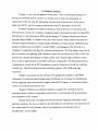
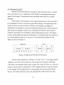
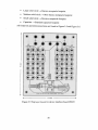
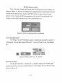
integrated circuit (IC) packages are shown in Figure 2.1 [2].
HaHH
oooo
oooo
o oo
oooo
:K
6-pin
Small Outline IC
SOIC
16-pin
Quad Flat Pack
QFP
cUHH]-D-h
16-pin
Leadless Chip Carrier
LCC
^
^
^
i^—
15-pin
Ball Grid Array
BGA
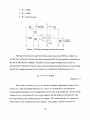
Figure 2.1 Modem integrated circuit (IC) packages
Having an existing product in a Chip Scale Package (CSP) was the starting point
of this thesis. According to IPC (Association Connecting Electronics Industries), the
package area of a CSP is less than 1.2 times its die area. When the package-to-die size
ratio is more than 1.2 and only solder balls are the board-level interconnect, the device is
called a BGA (Ball Grid Array) instead of a CSP. This is not always true because pitch
can also be used to classify a product as CSP. For example, Fujitsu's MicroBGA is a CSP
because of its fine pitch of 0.8mm even though its package-to-chip size ratio is more than
1.2. Hitachi Cable's Micro Stud Array Package (MSA) does not fit the CSP definition,
but it is also considered CSP because of its fine pitch stud array of 0.5mm. Therefore for
a device to be classified as CSP most have either one or both of the characteristics listed
below [3].
•
Package-to-chip size ratio less than 1.2
•
Pitch of less than 1mm
CSPs are then classified into four groups as follows [3].
•
Customized-lead-frame-based-CSP or Lead On Chip (LOG)
•
CSP with flexible substrate or Chip On Flex (COF)
•
CSP with rigid substrate
•
Wafer-level redistribution CSP
LOG'S
purpose is to increase the die-to-package size ratio for lead-frame-based
packages. CSP with a flexible or rigid substrate utilizes an interposer to redistribute the
original die level pitch to a standard CSP pitch (0.5, 0.65, 0.75, 0.8 or I mm) singularly
(after dicing the wafer). Wafer-level redistribution CSP uses a metal layer instead of a
substrate for pitch redistribution on the wafer [3].
CSPs have different characteristics from each other. Some of them can be seen in
Table 2.1. The highlighted terms in Table 2.1 indicate particular characteristics of the
Device Under Test (DUT) OPA2347 in CSP. The suffix YED is added to OPA2347 to
specify that the product is in CSP. A more complete description of the physical and
electrical characteristics of the DUT is explained later.
Table 2.1 Some CSP characteristics
Package-to-chip
size ratio
Pitch (mm)
CSP group
r'-level
interconnect
Board-level
interconnect
Terminals location
Terminals
distribution
Chip orientation
Packaging level
<1.2mm
>1.2mm only if pitch <lmm
0.5
LOC
0.65
Flexible Substrate
0.75
Rigid substrate
Wire
bonds
C4 solder
joints
C-lead
Metallization
(Sputtering/Electroplating)
Stud bumps
Plated flat lands
Inner Lead
Bonding (ILB)
Ribbonlike
flexible leads
Solder bumps
Plated
bumps
Top
Array
Solder pads
Solder balls
Bottom
Frame
Sides
Mirror
Face up
Wafer
Face down
Singulated
0.8
1
Wafer-level
redistribution
Solder
bumps
Thin film
deposition
Solder
Solid
core
studs
metal
spheres
Cu bumps
2.3 Development of the operational amplifier
The main purpose of an Operational Amplifier (Op Amp) is to achieve
mathematical functions. The Op Amp can be used to add, subtract, take the derivative
and integrate depending on the configuration of elements connected to it. Its design is
based on a three terminal active semiconductor device called a transistor. Bell
Laboratories invented the transistor in 1947. This invention replaced the use of vacuum
tubes, which was the only technology, at that time, capable of amplifying and detecting
electric signals since 1907. In the early days of electronics the electrical system used to
do mathematical operations was called an analog computer. Today's fabrication is based
on silicon, which is the most popular material used in the production of integrated circuits
(IC). An integrated circuit is defined as a combination of circuit elements interconnected
on a semiconductor material [1].
Texas Instmments (TI) was one of the first companies to manufacture transistors.
TI developed a small radio in 1954. Around 100,000 radios were sold during 1955 for
$49.99 each. U was the first radio based on transistors in the market [1].
2.4 Definition of the operational amplifier
The operational amplifier is a high gain active element that can be configured
with other elements to perform a specific function. Op amps have two differential inputs,
one output and two power supply inputs. Since the op amp can amplify AC signals; the
op amp is characterized as an active element. Passive elements, such as resistors,
capacitors and inductors, only absorb energy. An active element can provide AC energy
by converting the DC energy of its power supplies. Figure 2.2 shows the symbol for the
Op Amp.
Positive polarization
Negative input
Output
o
Positive input
I Negative polarization
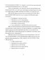
Figure 2.2 Symbol of the operational amplifier.
2.4.1 Real operational amplifier
To understand the real behavior of the Op Amp it is necessary to know some
properties of its terminals.
The output voltage (Vout) of the Op Amp cannot be more than its polarization
voltages (V+ and V-). Another important relationship for Vout is established in Equation
2.1.
Vout = -A(V,-V2)
Equation 2.1
The high gain, A, has a typical value of 10^ V, is the negative input and Vj is the
positive input. V, and V. have a high impedance input of 10'^i2. The potential difference
between the two inputs (Vi-Vi = Ve) is in the range of 10"^ to 10"^ volts.
Current flowing into the input terminals has a magnitude of 10''^ amperes. It is
called bias current (Ig).
These characteristics have values that are either too small or too large in
relationship to the other parameters in the circuit. This makes it possible to model the Op
Amp as an ideal operational amplifier. As a consequence, circuit analysis becomes easier.
An explanation of the properties of the ideal operational amplifier is given in the
next section.
2.4.2 Ideal operational amplifier
The ideal operational amplifier has the following characteristics [1].
•
IB-H
= IB- ^
0
•
A - ^ o=>
•
(Vi V2) —> 0 (Condition only satisfied with negative feedback)
Due to IB for both inputs —> 0, the input impedance —> 0°. If there is negative
feedback in the network, the infinite gain causes the inputs to be consider as virtually
connected with zero resistance. In this case, if the positive input is grounded, the negative
input is virtually grounded. With this principle, many useful circuit configurations can be
developed. Even though the gain is considered to A —> «>, the output value is limited by
the supply voltages.
2.5 Device under test (DUT)
The device under test (DUT) OPA2347YED is a dual CMOS (Complementary
Metal Oxide Semiconductor) operational amplifier in a chip scale package (CSP). The
suffix YED indicates that the device is CSP. Its main DC electrical characteristics are low
power consumption with a quiescent current (IQ) of 20|iA per amplifier, a single or split
supply from 2.3V to 5.5V and rail-to-rail inputs and outputs [4].
8
2.5.1 Product data sheet only with DC parameters to be tested
Table 2.2 contains the DC parameters to be tested with their abbreviated names.
The condition column establishes test requirements for every test to ensure results within
maximum (max) and minimum (min) limits. These limits, if present, are guaranteed
values. Typical values are not guaranteed. They were calculated by design to give a
reference.
Table 2.2 Product data sheet DC parameters of the OPA2347
•Parameter
Input ol'fset \oltage VQS
Power-Supply Rejection Ratio PSRR
Common-Mode Rejection Ratio CMRR
Input Bias Current IB
Input Offset Current IQS
Open-Loop Voltage Gain AQL
Voltage Output Swing from Rail
Quiescent Current (per amplifier) IQ
Condition
Vs=5.5V
VcM=(V-H0.8V
Vs=2.5V to 5.5V
VcM<(V+)-1.7V
Vs=5.5V
(V-)-0.2V<VcM<{V+)-1.7V
(V-)-0,2V<VrM<(V+)+0.2V
Vs=5.5V
RL=100kQ
0,015<Vo<5,485V
RL=100kQ
AoL>100dB
Io=0
Min
Typ
2
Max
6
Units
mV
60
175
laV/V
70
80
dB
±10
±10
100
±0.5
±0-5
115
pA
pA
dB
5
15
mV
20
34
HA
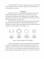
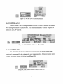
Figure 2.3 represents the top view of the typical input/output (I/O) pin
configuration for this dual operational amplifier. All previous packages of the OPA2347
have leads to perform board level interconnections. The number and name of every
terminal are shown in Figure 2.3.
L*J
to
-
-VS
+IN A
-IN A
OUT A
+IN B
-IN B
OUT B
+VS
.^
LA
Ov
--J
00
Figure 2.3 Typical top-view configuration of a dual op amp
2.5.2 Package of the DUT
Because the OPA2347YED has a package-to-chip size ratio less than 1.2 and its
pitch is less than 1mm, it is categorized as CSP. Wafer level packaging technology is
applied to this product. This means that after sawing the wafer the device is already
packaged.
This location of the bond pads on the original integrated circuit (IC) layout had to
be reconfigured in order to meet bump on pad CSP technology. The original pads were
located in line on one side of the die to facilitate wire bonding for packaging. IC
redistribution was required to extend interconnections between active circuitry and bond
pads for this new package in order to have a final pitch of 0.5mm. In other words, the
original IC layout had to be reconfigured without modifying any circuitry. The original
circuitry did not suffer any functional modifications. To facilitate metal trace extension to
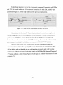
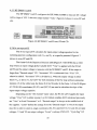
the corresponding bond pad, it was necessary to rotate operational amplifier B 180
degrees as shown in Figure 2.4.
Original die
CSP die
m
OP AMP A
OP AMP B
m
OP AMP A
mssfflHiss
a
a
m
m
a dwv do
g]
Q]
Figure 2.4 Original and CSP OPA2347 die layout
The area of the original die is 358.8nm *1731.2|xm. On a 6" wafer approximately
14,000 die can be built. On the other hand, CSP die had to be increased to 888.85|xm
*1981.2nm to accommodate solder bumps on pads with a pitch of 0.5mm. As a resuU, the
number of die per wafer was decreased to 7,500. It appears that the cost per die increases
for this package, but the original die has to be packaged after sawing and the CSP die
does not. This makes wafer level chip scale packaging (WL-CSP) cheaper than other
10
conventional packaging techniques. It is important to note that the pitch and solder bump
size determine the minimum die area for a CSP product.
Wafer-level redistribution is the CSP group to which the OPA2347YED belongs.
This group defines the way to interconnect solder bumps to existing I/O pads at the wafer
level. Redistribution layer (RDL) and Bump On Pad (BOP) are two approaches used.
RDL and BOP require a passivation layer on top of the active circuitry. Then a
Benzocyclobutene (BCB) repassivation layer is required. This BCB polymer layer
provides [5]:
•
Reconfiguration of perimeter I/O pads,
•
Planarization of a severe surface topology,
•
Size reduction of perimeter I/O pad openings,
•
Stress buffer or scratch protection,
•
Lower coupling between redistribution lines and active circuitry.
RDL is a metal layer deposition and patteming technique utilized to interconnect
existing I/O pads to a solder-bump array. IC layout reconfiguration is not required. Solder
bumps are placed on top of this redistribution layer. RDL was not an option for the
OPA2347YED. BOP was used instead because die reconfiguration was possible without
affecting the circuitry's functionality [5].
BOP requires IC layout reconfiguration to meet CSP specifications. This is the
case of the OPA2347YED. An Under Bump Metallurgy (UBM) is placed on top of the
pad before solder bump deposition. UBM's diameter for the OPA2347YED is 247nm.
UBM provides [5]:
•
A solder wettable terminal,
•
Size and area of the solder connection,
•
Adhesion between solder and chip,
•
Diffusion barrier between solder and chip,
•
Electrical contact to the chip I/O.
11
Solder bump placement is the last procedure to complete. Composition of 63% Sn
and 37% Pb is used in this case. Cross section illustrations for both RDL and BOP are
presented in Figure 2.5 [6] to help understand the previous explanations.
/ solder bump \
/ .„M«,K,.™A
URM/-^
_
passivation
^
^ — ^
,
repassivation
_ 1
1 •
pad
y
redistribution
active circuitry
active circuitry
silicon
silicon
BOP
1
1 _
RDL
Figure 2.5 Cross-section illustrations for BOP and RDL
Since this is the first time TI-Tucson has introduced an operational amplifier in
CSP, a comparison with its first competitor will be discussed. National Semiconductor
produces the LM2904 in a micro Solder Mask Defined (uSMD) package. Although
National Semiconductor is in the head of CSP technology, the electrical and mechanical
performance of the LM2904uSMD does not surpass the OPA2347YED [4] [7].
Starting with the I/O array of 2*4 bumps, the OPA2347YED resembles the
conventional pin out for a dual op amp. This is an advantage to the customer since they
will be dealing with an identical pin out configuration previously used with the same
product in a different package. On the other hand, the LM2904uSMD has an I/O array of
3*3 bumps without a center bump. Figure 2.6 and Figure 2.7 identify the outlines of these
products [7].
0.143mm
2.086111111
0.25mm
,
n
r-— 0.5mm
i
>
0.5mm
t
0.9936mm
0.0968mm
Top view
sey^Dz
00.3mm
Bottom view
0.3896mm
T
I
0,6096mm
Front view
0.22mm
Figure 2.6 OPA2347YED outline
Bump diameters of 0.3 mm against O.I6-0.18mm is another advantage for the
OPA2347YED because the larger the bump size makes for easier assemble and visual
inspection. Even though both have a pitch of 0.5 mm, the LM2904uSMD occupies more
area because of its center bump [7].
1.45mm
\ -' \ .^ \ ^
/
\
1.45mm
Top view
Figure 2.7 LM2904 uSMD outline
Power consumption is a key factor for a product because the larger the quiescent
current (Iq) the more expensive to keep the device working. The OPA2347YED
consumes 25 times less power than the LM2904uSMD. The electrical performance for
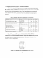
both components is illustrated in the following table [4, 7].
13
Table 2.3 Electrical performance of LM2904uSMD and OPA2347YED
Parameter
Quiescent current
Input bias current
Input offset voltage
Power supply rejection ratio
Cominon mode rejection ratio
Bandwidth
Slew rate
LM2904uSMD
500 nA
40 nA
2mV
100 dB
70 dB
1 MHz
0.5 v/^s
OPA2347YED
20|.iA
±0.5 pA
2mV
85 dB
80 dB
350 MHz
0.I7V/HS
2.5.3 Applications
There are a variety of applications for this product including portable equipment,
battery-powered equipment, two-wire transmitters, smoke detectors and CO detectors [4].
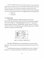
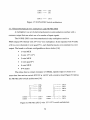
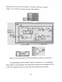
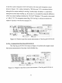
2.6 Testing DC parameters
2.6.1 Test circuit
Testing DC parameters of a dual operational amplifier is not an easy task.
Different circuit configurations and conditions can be applied per parameter. As a result,
a general test circuit shown in Figure 2.8 will be used to meet configuration requirements
for every test.
Particular circuit configurations for every test can be obtained by closing specific
relays of the general test circuit. Consequentiy only the circuit needed to test each
parameter will be displayed and explained. In order to occupy less figure area, two labels
separated by a coma or one above the other will differentiate the elements and pins of op
amps A and B. Closed relays, parameter definitions, test conditions, with an explanation
and special considerations are also included based on OPA2347YED data sheet
specifications.
The false summing junction configuration, consisting of five resistors and
negative feedback, is used to set the output of an op amp to a desired level by adjusting
the input of the circuit [8]. Predominance is granted to this circuit shown in Figure 2.12
because it will help to test the majority of the parameters.
14
Capacitors are connected as close as possible to each power supply pin of the
DUT to ground in order to maintain the voltage applied to each terminal stable. These are
called decoupling capacitors.
V(M R
RU
Rl-J.irM2%
*• KKI iI i. .I K
c 'm
in
<^'^(s>
r
-T ®
MAX VrjAKJJ
\Rn.iriM
2ii'>ii
i
KiAx®}
1
,s.(S)
SA
L>
kI:C VM.
'
hA
\-^Rrr. \ M
SB
^^17
®"
C
^
VODRO"
Rtl.l(.Hi2*\
^ Rf 1ICM13
IXSJ.LNA
,
^
6R
JITB(5)
^
OITB(#)
HTA
^
I
-fc
^
OlTAfi
> IHH.
RiA
-O"
-r-"jKH'.Mi|
R l » \ VOIiREF,
;i)Op
n^"'^
KR
T
RhCJ2R(
^°
1-^
K.-rt
^ " ^
(^^niTB
>
o n
(i)n
®-X T
r
T
T, T
-r
"® 1 ^~§)
,...o(S) p
rc-
(s) ^ 4
"•^11
SCmiW 1
M.'KI;"W2
^
si-Kf.'A '
..M,(S)
4
H CREW 4
Figure 2.8 General test circuit
MUXCHxx represent the places where voltage and current measurements must be
taken. MUXCHO to MUXCH7 are for voltage. MUXCH12 to MUXCH13 are for current.
VCHx indicates the points where voltages are applied. Since this circuit is implemented
on a printed circuit board, circle symbols point out the terminals where resistors,
15
capacitors, relays (RELxCHxx), multiplexer relays (MUXCHxx) and instruments must
be connected. The test temperature is 25°C.
2.6.2 Verification routine
Definition: The verification routine verifies if the power supply (AO) and digital
multimeter (DMM) are setting and measuring voltages without exceeding an error of
lOO^V (DMM) and 350|LiV (AO) with respect to a well known calibrated DMM.
Closed relays: None
Test circuit configuration: None
Test conditions: Connect DMM 1 and DMM 2 in parallel.
Steps: Apply 3 voltage levels (-5, 0 and 5 V) per each voltage channel VCHO,
VCHl, VCH2 and VCH3 while measuring them with both DMM 1 and DMM 2 through
MUXO, MUX3, MUX6 and MUX7. Having DMM 2 as a reference, readings taken from
DMM 1 and the desired voltage level cannot differ by more than
IOOJAV
and 350p,V.
Special considerations: Make sure all instmments have the same ground
reference.
2.6.3 Quiescent current test (In)
Definition: Power supply current of the op amp when its output current is zero
[8].
Relays in use: REL1CH3, REL1CH5, REL1CH8, REL1CHI3, RELICH15, ,
REL2CH2 and REL2CH5.
Test circuit configuration: Voltage follower shown in Figure 2.9.
Test conditions: No load
Expected value: 40^A (20nA per amplifier).
Steps: Apply Vs-^=2.75 V, Vs-=-2.75V, close all relays in use and then measure
MUXCH12 current. Divide this reading by 2 to obtain IQ per amplifier.
Special considerations: Verify if the op amp is oscillating with the use of an
oscilloscope connected to the output. If the op amp oscillates due to parasitic elements on
16
the DIB, a pole-zero analysis previously done by the designer of the DUT must be
studied to correct this problem.
Figure 2.9 Quiescent current (IQ) test circuit
2.6.4 Positive input bias current (W)
Definition: The current flowing into the positive input of the op amp [8].
Test configuration: Stop watch integration shown in Figure 2.10.
Relays in use: REL1CH3, REL1CH5, REL1CH8, REL1CH9, REL1CH13,
REL1CH15, REL2CH2, REL2CH3, REL2CH4 and REL2CH5.
Test conditions: RL=R5=100kfll and C2=200pF.
Expected value: ±0.5pA.
Steps: Apply Vs+=2.75 V, Vs-=-2.75V, close all the relays, open the relay
REL1CH8/REL2CH2, wait for signal settiing AsTART>10ms before taking
AT>500ms, measure
VOUT2
and then compute
VQUTI,
IB-H=-C2*(VOUTI-VOUT2)/(AT).
wait
The negative
sign corrects polarity of the input bias current.
Explanation: Since the current to be measured is in the order of pA and a DMM
capable of measuring it is very expensive, a capacitor is used to integrate this current over
a period of time (Aj) to obtain the corresponding voltage change
(VQUTI-VOUT2)-
The
relationship of the voltage and current through a capacitor is Vc=C*Ilc*dt. C2=200pF
17
was calculated by using the typical value for lB-^=0.5pA, and choosing AT=lsec and
(VoiiTi-VoiiT:)=2.5mV.
Special considerations: Connect an oscilloscope at the output to verify the circuit
is integrating properly without leaking, saturation or oscillation. Leaking increases the
voltage rate of change at the output resulting in a higher measurement. Saturation
produces a zero measurement because the output would reach either of the supplies in
less than 100ms once the relay is open. Oscillation generates a sine wave at the output of
the op amp. Accuracy can be improved by incrementing At or decrementing C2. Both
ways minimize noise by allowing a larger
(VQUTI-VOUT2)-
Capacitance reduction is a
concem when on-board parasitics of the same value are present. When measuring pA a
glass capacitor is preferred due to its better performance with respect to any other type.
REL1CH8 I
REL2CH2 o^
RSA ^ M U X C H 6
^^^ ^ ^MUXCH7
C2A
L^K
Figure 2.10 Positive input bias current (IB+) test circuit
2.6.5 Negative input bias current (IR-)
Definition: The current flowing into the negative input of the op amp [8].
Test configuration: Stop watch integration shown in Figure 2.11.
Relays in use: REL1CH3, REL1CH4, REL1CH5, REL1CH8, REL1CH9,
REL1CH13, REL1CH14, REL1CHI5, REL2CH2, REL2CH3, REL2CH4 and
REL2CH5.
Test conditions: RL=R5=100kQ and Cl=200pF.
Expected value: ±0.5pA.
18
Steps: Apply Vs,=2.75 V, Vs.=-2.75V, close all the relays, open the relay
REL1CH3/REL2CH13, wait for signal settling A.sTART>10ms before taking
measure
VQUT:
after waiting AT>500ms and then compute
VQUTI,
IB-=C1*(VQUTI-VQUT2)/(AT).
Explanation: Although the capacitor for this test is connected from the output to
the negative input of the op amp, the same principle used to obtain IB+ is applied for IB-.
Special considerations: Nearby circuitry other than the one in use can be a source
of noise. Although glass capacitors are very expensive they provide the best performance
for this test.
VCH2
„ „,
REL1CH3 \
8 ( V S 0REL2CH13.f
REL2CHI3,\
z^ClA
T "CIB
C I B
^ ^
17
Op Amp A, B > — - —
3,5
"*"
VOUT
RCA /v^MUXCH6
R5B V M U X C H 7
^ 4 (Vs.)
)VCH3
Figure 2.11 Negative input bias current (IB-) test circuit
2.6.6 Input offset current (Ing)
Definition: The difference between IB-I- and IB- [8].
Expected value: Less than ±0.5pA due to the expected values for IB-H and IB- are in
the same range.
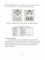
2.6.7 False summing junction test circuit
The false summing junction configuration will be used to test the rest of the DC
parameters. Five resistors and negative feedback form the basic idea of this circuit
illustrated in Figure 2.12. Both VCH2 and VCH3 can be positive or negative depending
on the test conditions [8].
Values for all resistors are shown below:
•
R, = R2 = lOOk^
19
•
R3 = lOkQ
•
R4 = lOOQ
•
R5 = disconnected
y)MUXCH4
/T)VCH2 R2A
RSA (VjMUXCH6
MUXCH7
Figure 2.12 False summing junction test circuit
The load resistance RL specified in the product data sheet (PDS) is lOOk^. It is
not the one connected between the output and ground (R5) but the parallel combination of
R2 and R5 (RL=R5I I R2=100ki2). Therefore if choosing R2=100kQ, then R5 must be
disconnected. With these resistor values and considering the ideal behavior of the op amp
(IB-=0),
the voltage between the two inputs
VIN
is amplified (l-)-R3/R4) times at Vx.
ViN=Vx/(l+R3/R4)
Equation 2.2
This circuit is used to set VQUT at a desired voltage by adjusting the input of the
circuit (Vi). The relationship between
VQUT and VJN
is essential for calculating the
remaining DC parameters. Even though the positive input is grounded, the common mode
voltage (VCM) is not always OV as for split supplies but the difference between OV and
the output being at the middle point of the supplies. This means that the VCM applied is
with respect to the middle point of the supplies. The supplies used for each test are
20
specified in the PDS with respect to an initial VCM- Since the positive input for the SIC is
grounded, this initial
VCM
is OV. Substitute
VCM=OV
to obtain the supplies per test. Vs is
the difference between the positive (Vs-^) and the negative (Vs-) supply.
Relays closed for this circuit are RELICHO, REL2CH6, REL1CH6, REL1CH2,
REL1CH8, RELICHIO, REL2CH7, REL2CH0, REL1CH12, REL2CH2, REL2CH4 and
REL2CH5.
2.6.8 Input offset voltage (Vns)
Definition:
VDM
when
VQUT is
Test conditions: Vs=5.5V,
at the middle point of the two supplies [8].
VCM=(V-)+0.8V
Expected value: 2mV
Steps: Apply
VS-H=4.7V, VS-=-0.8V.
measure Vx to calculate
adjust the input to set the output at 1.95V,
VIN=VQS.
Explanation: Measuring the input offset voltage is the easiest test but it varies
with the common mode voltage (VCM) applied to the positive and negative input. By
setting the output at the middle point of the supplies when adjusting the input as specified
in the test conditions, a VCM of -1.95V is obtained.
2.6.9 Power supply rejection ratio (PSRR)
Definition: The change of VIN with Vs [8].
Test conditions: Vs=2.5V to 5.5V,
VCM<(V+)-1.7
Expected value: 60|J.V/V.
Steps: Apply Vs+=3.3V=Vsi+, Vs-=-2.2V=Vsi., adjust the input to have VQUT at
0.55V, measure Vx to calculate
the input to have
VQUT
VIN=VINI.
Set Vs+=1.8V=Vs2+, Vs-=-0.7V=Vs2-, adjust
at 0.55V. measure Vx to calculate
VIN=VIN2,
compute PSRR as
shown in Equation 2.3.
PSRR = (ViNi - V,N2) / 2(Vsi+ Vs2+)
Equation 2.3
21
Explanation: PSRR is used to measure the ability of the op amp to reject a
symmetrical change in Vs reflected at V,N. The VCM remains at the same level
(VcMi=VcM2=-0.55V) when changing Vs to eliminate the VCM contribution in the PSRR
calculation. This is obtained by changing the supplies symmetrically.
Special considerations: Make sure decoupling capacitors are connected as close as
possible from 'Vs+ and Vs- to ground.
2.6.10 Common-mode rejection ratio half scale (CMRRh)
Definition: The change of VIN with VCM at half scale [8].
Test conditions: Vs=5.5V, (V-)-0.2V<VCM<(V-I-)-1.7
Expected value: lOO^iV/V (80dB).
Steps: Apply VS-I-=5.7V=VSI-H, VS-=0.2V=VSI-, adjust the input to have VQUT at
2.95V=-VCMI,
measure Vx to calculate VIN=VINI. Set Vs-H=1.7V=Vs2-f, Vs-=-3.8V=Vs2-,
adjust the input to have VQUT at -1.05V=-VCM2, measure Vx to calculate VIN2, compute
CMRRh as shown in Equation 2.4.
C M R R h = (ViNl - ViN2) / (VcMl- VCM2)
Equation 2.4
Explanation: CMRR is used to measure the ability of the op amp to reject a
change in the VCM reflected at VIN. The VCM is not kept at the same level when changing
the supplies. The supplies are moved asymmetrically keeping Vs fixed to eliminate the
supplies contribution in the CMRR calculation. The VCM change of 4V serves to classify
this CMRR measurement as half scale.
2.6.11 Common-mode rejection ratio full scale (CMRRf)
Definition: The change of VIN with VCM at full scale [8].
Test conditions: Vs=5.5V, (V-)-0.2V<VCM<(V+)+0.2
22
Expected value: 316.227|iV/V (70dB).
Steps: Apply Vs+=5.7V=Vsi+, Vs-=0.2V=Vsi-, adjust the input to have VQUT at
2.95V=-VcMb measure Vx to calculate V,N=VINI. Set Vs+=-0.2V=Vs2+, Vs-=-5.7V=Vs2-,
adjust the input to have VQUT at -2.95V=-VCM2, measure Vx to calculate ViN=VnM2,
compute CMRRf as shown in Equation 2.5.
CMRRf = (VIN,-ViN2)/(VcMi VCM2)
Equation 2.5
Explanation: The VCM change of 5.9V serves to classify this CMRR measurement
as full scale.
2.6.12 Open loop voltage gain (Anr)
Definition: The change of VQUT with VIN [8].
Test conditions: Vs=5.5V, (V_)+0.005V<VQUT<(V+)-0.005V
Expected value: 1.778^V/V (115dB)
Steps: Apply Vs-^=2.75V, Vs-=-2.75V, adjust the input to have
VQUT=2.74V=VQUTI,
measure Vx to calculate VIN=VINI, adjust the input to obtain
VQUT=-2.74V=VOUT2,
measure Vx to calculate VIN=VIN2, compute AQL as shown in
Equation 2.6.
AQL = I (VQUTI
VOUT2)/(VINI
V1N2) I
Equation 2.6
Explanation: The name of this measurement infers that the op amp must be in
open loop in order to measure a change in VQUT with VIN- This circuit configuration is not
possible because if applying a VIN of ±lmV, which is the typical accuracy of a DMM, the
output would be limited by either of the supplies instead of being amplified 562429.69
times. Therefore a fix voltage change in the output divided by the corresponding change
23
in ViN is used for the AQL calculation. Notice that the swing condition for this test (more
than 5mV from the rail) is not the same specified in the PDS (more than 15mV from the
rail). This is because the op amp can actually swing to 5mV, based on data collected,
maintaining a linear relationship between the output and the VQS.
2.6.13 Voltage output swing from rail (SWom±]
Definition: The maximum voltage the output of the op amp can swing from each
rail maintaining a linear relationship with respect to VQS.
Test circuit configuration: Summing junction configuration when the open loop
gain is performed.
Test conditions: RL=R5=100ka, AoL>100dB
Expected value: 5mV (15mV maximum)
Steps: Obtain a plot of VOUT versus VOS by adjusting the input. Determine the
values for VQUT in which the plot becomes not linear. These values are the positive and
negative voltage output swing from rail. Since this technique is time consuming, one can
only do a pass/fail test by setting the output of the op amp at least 15mV from the rail by
adjusting the input and verify if the output can be set in that range, otherwise the device
fails for this parameter.
Explanation: Since the output set in the AQL test is in the expected range for this
parameter, the positive and negative voltage outputs of the op amp used to calculate AQL
can be used to verify if the output can swing at least 15mV from each rail.
24
CHAPTER 3
TEST HARDWARE
3.1 Socketing the DUT
Socketing and surface mounting a device to adapter boards serve to make
electrical contact to the I/O. One is as important as the other. Although the customer is
going to solder the component to a printed circuit board (PCB), it is cheaper to use a CSP
socket for testing. Assembling only 20 units on adapter boards equals the price of a CSP
socket. The OPA2347YED is tested on adapter boards and also with a clam shell type
CSP socket having springs to provide the board level interconnection. Thus the CSP
socket IS not soldered to the device interface board (DEB) but mechanically attached with
four nuts. This feature protects the DIB from socket replacement because unsoldering
usually causes damage. Edge connector and dual in line package (DIP) are the socketing
versions for the adapter boards.
3.2 Printed circuit board design
3.2.1 Protel
Protel is the software utilized to design the printed circuit boards. The purpose of
this section is not to explain how to use the software, but to provide the key steps to
generate a PCB layout from a circuit schematic.
One project database file stores as many schematic, layout, schematic library or
layout library type files as wanted. A schematic file contains any kind of circuit diagram.
It is built with symbols created and stored in schematic libraries. A layout file is a bylayer physical representation of a circuit diagram. Schematic and layout can be either
independent or mutually synchronized so that any change performed in one is updated in
the other. It is always easier to draw the schematic first and then Protel generates the
layout. For doing this, the user must type on every symbol placed on the schematic file its
layout symbol reference. Nodes are also synchronized [9].
25
Once every symbol of the layout, also called the footprint, has been oriented and
located, the trace width has to be set. All interconnection nodes are automatically traced,
based on layout rules, when the autoroute command is activated. Then, traces are
manually corrected and revised with the error checklist command. Finally, the following
files along with board characteristics have to be zipped and sent to the manufacturer [9].
•
Gerber files
•
NC drill files
3.2.2 Adapter boards
As previously mentioned, two adapter boards are used to attach the
QPA2347YED and make electrical contact to the I/O. The circuit schematic created for
both is shown in Figure 3.1. Three symbols appear on that circuit. "C" represents the
capacitor footprint of the layout. "DESIGNATOR" represents either the 2*4 hole array
for the DIP version or the two-sided 4 pad array for the edge connector type. "QPA2347"
represents the footprint of the OPA2347YED.
Figure 3.1 Schematic for adapter boards
Then PINl to PIN8 labels next to every interconnection wire serves for node
identification. This is necessary when performing layout generation based on this circuit
schematic.
Top and bottom layer drawings for both adapter boards are shown in Figure 3.2
and Figure 3.3. The capacitor footprint allows either surface mounted or lead based
26
technologies. Plated holes are indicated as solid black circles with gray contour. Holes
are simply solid black holes. CSP pads are solid gray circles with black contour. The 2*4
DIP plated hole array for board PR791 is where pins are inserted and solder to make
electrical and mechanical contact to a DIP socket.
E3
€3
•
•
•
•
•
•
PR79118888<
10 (mm)
•
>
C
•1
•
V ^''\ m
•
•
•
«
10 (mm)
Figure 3.2 Top and bottom layer layout for DIP adapter board PR791
The black contour around CSP pads specifies that the solder mask opening has to
be larger than the pad size. It is called non-solder mask defined (NSMD). NSMD
prevents solder bridging among solder balls when reflowing is performed. Reflow is the
process used to solder the CSP to the board. It consists of applying solder paste on pads,
placing the CSP on top of them and generating air hot flux to solder every ball to its
respective pad. The amount of solder paste as well as the pad size are based on ball size.
The pad size diameter in this case is 0.275mm and solder mask opening is 0.375mm [10].
It is important to know how much down pressure the assembly house will apply
when handling the CSPs. Cracks on silicon may be caused if the pick and place piece of
equipment is not set up properly. The QPA2347YED handles a pick and place down
force of 80 grams (lOgrams/ball).
Board PR792 (edge connector) is not a common way to adapt a device but a more
economical solution. Buying and assembling pins is eliminated with this version.
Fabrication cost may be more expensive in comparison with board PR791 (DIP) but the
27
final cost, including assembly, is less. Four plated holes called vias connect the top and
bottom layers. Characteristics for boards PR791 and PR792 is in Table 3.1.
12 544 (mm) •
12.544 (mm) •
Figure 3.3 Top and bottom layer layout for edge connector adapter board PR792
Table 3.1 Adapter board characteristics
Characteristic
Board material
Board thickness
Trace material
Trace thickness (T)
Trace width (W)
Mask type
CSP pad diameter
Land pattern
NSMD diameter
Value
Polyimide
1.5748mm (62mil)
Immersion gold
25.4nm(lm]l)
0.1524mm (4mil)
LPI-GREEN 2-Sides
0.275mm
Non-solder mask defined (NSMD)
0.375mm
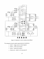
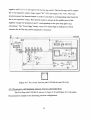
3.2.3 Device interface board
As previously stated, the test circuit is implemented on a printed circuit board
named bench board or device interface board (DIB). Three socketing options are included
on this board: edge connector, DIP and CSP Symbols for the circuit schematic shown in
Figure 3.4 were first created, placed, PCB layout related, and then interconnected
including node identifiers.
28
voA r " "
RIAX
-<3"®-
-®(^
RIAX
VINXA
•
RIAX
(i)R lAX
VX^f
lA
:A
) GND
VOARLI
DLIT2
J
R3A
GND(5)
\(»)
OUTA(5)
5A
(•)-lNA
6A
PIN
-(5) (•)
4A
- \ • )REC+V
R4A
11
®
5B
6B
(•)
OUTB(5)
^ -
GNDAW)+VSX:
wsfi) +v
VOB REF
OUTAHi)
7A
RlBX
TO
RlBX
RlBX
VlNXB
VXB(*)
IB
28
I CND
" ( * /
RECGND
-<55'(j)—r
( • )
RSA
CND
VOBREI
( • ) RlBX
GND
R3B
GNl/5)
R5B
Hl)lNB
OUTB
^
OPA2347
PIN 4 -VS
-™4 ^
GND(<»)
Vr^
(iriGND
Vr^
.NA(^S<i) VS(4
^
CND(»)
P\
GND(5)
=F T", T
,C6
T
^ ^
r±rC7
A ,
^i; i i
Cl^
SCREW 1
SCREW 2
SCREW 3
SCREW 4
Figure 3.4 Schematic for device interface board PR825
The schematic-to-layout symbol representations are listed below.
•
DUTl -^ Edge connector socket footprint
•
DUT2 -> CSP socket footprint
•
DUT3 -^ DIP socket footprint
•
Solid circle -^ Hole for screwing stand off
29
^-i-'CS
vO^cs
RHTJIL
•
Large solid circle -> Banana receptacle footprint
•
Medium solid circle -^ Mini banana receptacle footprint
•
Small solid circle -> Resistor receptacle footprint
•
Capacitor -» Standard capacitor footprint
All footprints and interconnections are found in Figure 3.5 and Figure 3.6.
I
•vs
y
UKU
y
^
r2i
GND y
-IN A
-IN A
^
KjAX
^ ^
••••••<•«•
"EH
ONI)
w
- v s « »•*»•'
f
n
V
J<J^\,*~.
'NB
-IN B
GNP
^^^
V
DUAL OP AMP AUTO DC TEST BOARD - CSP - PR825
14 (mm)
Figure 3.5 Top layer layout for device interface board PR825
30
I
VSY
I
^^^
KEF
VOA KEF
V( lA KEF
vry v _i y _
V(M KEF
VOB KEF
v o n REF
_
VOB REF
VOB RE
klA
^
VINXA
K ll A X
•)
^
\REF
'•'HtJ V.
^
A.> IN A
K1 A.X
•)
VOIH KEF
\REF
RIHX
(5
-V)
RlBX
-IN E
•••••• • »
I
D
5)
»)
C.
GIID
f
C2A
VI
i
M
i
DUAL OP AMP AUTO DC TEST BOARD - CSP - PR825
14 (ram)
Figure 3.6 Bottom layer layout for device interface board PR825
Table 3.2 summarizes the characteristics of the board PR825.
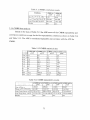
Table 3.2 Device interface board characteristics
Characteristic
• ''
Board material
Board thickness
Trace material
Trace thickness (T)
Trace width (W)
Trace width on DUT2 area (W2)
Mask type
Value
'.
•
FR4
1.574mm (62mil)
Hard body gold
25|am(lmil)
0.307mm (12mil)
12 mil (307|am)
LPI-GREEN 2-Sides
31
3.3 PXI svstem
3.3.1 Introduction
PXI means Peripheral component interconnect (PCI) extensions for
Instrumentation. U is a modular, computer-based instrumentation platform based on the
PCI bus. PCI is an industry-standard, high-speed databus. The elements of a PXI system
are listed below [11].
•
Controller
•
Chassis
•
Modules (cards)
A controller can be either a personal computer or an embedded Pentium class or
higher computer and peripherals. The main disadvantage between these two options is
price and speed. A personal computer can be four times less expensive, but also slower
than the embedded option. The embedded option can perform real time applications
because the system is dedicated to interact with the modules and nothing else [11].
A chassis is in charge of providing mechanical protection, ventilation, power
supply and interface to the modules inserted in it.
PXI modules are classified as multifunction boards and instruments. A
multifunction board can be of any type, like a general purpose relay switch, relay
multiplexer, analog-to-digital, digital-to-analog, image acquisition, motion control, etc.
Instruments can vary from digital multimeters, oscilloscopes, power supplies, spectrum
analyzers, and many others [11].
One way to interface a desktop computer with PXI modules is through a link
called MXI-3 consisting of a MXI-3 module, cable and PCI card [11].
External instruments like the high resolution 8V2 digit DMM HP-3458A or the 6'/2
digit DMM HP-34401A can communicate with the PXI chassis through a PXI general
purpose interface bus (GPIB) card. The instrument receives and sends GPIB commands
from and to the controller to perform a specific function [11,12,13].
32
The controller and modules from National Instruments (NI) utilized to test the
OPA2347YED with a NI PXI chassis are explained in this section and listed below.
1
MXI-3 link
1
18-module PXI chassis
1
GPIB module with Ethemet port (NI PXI-8212)
2
General purpose relay switch card (NI PXI-2565)
1
Electromechanical relay multiplexer card (NI PXI-2503)
1
6'/2 Digital multimeter (NI PXI-4070)
1
Analog output (NI PXI-6704)
The interconnection among modules and DIB is also covered.
3.3.2 Controller
A personal computer (PC) is the controller for the automated bench system. A
Pentium I running at lOOMHz with 96Mb of RAM is good enough for the tester. The PC
communicates with the PXI modules through a MXI-3 Unk.
3.3.3 18-slot PXI chassis (PXI-1006 chassis)
In order to have extra slots for future modules, an 18-slot PXI chassis was chosen.
The current system comes with PXI and CompactPCI module capability and only
occupies 9 slots. Modules are easily plugged into the system, like drawers into a desk.
Before connecting the chassis with the MXI-3 cable to the computer, all drivers must be
installed on the PC. The PC is turn on after the PXI system, so that all inserted modules
are recognized [14].
3.3.4 General purpose relay switch card (NI PXI-2565)
The NI PXI-2565 is a I6-channeI general purpose electromechanical relay switch
card. The relays can switch 30V DC at 5A DC with a resistive load. They have a contact
resistance of 30mQ and operate (open or close) in no more than 10ms. Figure 3.7 shows
the NI PXI-2565 switch architecture [15].
33
COMO
COMl
CHO
CHI
C0M15 - ^ ^ —
CHI5
Figure 3.7 NI PXI-2503 Switch architecture
3.3.5 Electromechanical relav multiplexer card (NI PXI-2503)
A multiplexer is a set of electromechanical or semiconductor switches with a
common output that can select one of a number of input signals.
The NI PXI-2503 is an electromechanical relay multiplexer card in a
PXI/Compact PCI format with 24* 1 two-wire multiplexer. It also operates with 4 banks
of 6 two-wire channels (2-wire quad 6*1), each bank having its own common two-wire
output. The board is software-configurable as shown below [16].
•
1-wire MUX
•
2-wire 12*1 12*1
•
2-wire MUX
•
2-wire quad 6*1
•
4-wire MUX
•
6*4 matrix
The relays have a contact resistance of lOOmQ, operate (open or close) in no
more than 5ms and can switch 30V DC at 1A DC with a resistive load. Figure 3.8 shows
the NI PXI-2503 switch architecture [16].
CHI 2+
CHICHI 3+
CH13-
CHO+
CHOCH1+
CHl-
COM0+
COMO-
C0M2+
COM2-
CH11+
CHll-
CH23-(CH23-
Figure 3.8 NI PXI-2503 2-wire 12*1 12*1 switch architecture
34
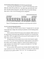
The NI PXI-2503 has a front panel 68-pin female connector. Table 3.3 shows the
pin assignments. The NI TB-2505 is a front panel mounting screw terminal block that is
plugged into the female connector in order to electrically access the channels, common
terminals and other pins of the NI PXI-2503. The pin assignments for the two-wire mode
using the NI TB-2505 are shown in Table 3.4 [16].
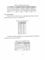
Table 3.3 NI PXI-2503 front connector pin assignments for two-wire mode
Pin name
CJSOCHOCHICH2CH3CH4CH5COMOCOMICH6CH7CH81_W1RE_L0_REF
CH9CHIOCHllABOABICH12CH13CHI4CHI5CHI6CH17C0M2COM3+5 V
GND
CHI8CH19CH20CH21CH22CH23-
Pin#
34
33
32
31
30
29
28
27
26
25
24
23
22
21
20
19
18
17
16
15
14
13
12
11
10
9
8
7
6
5
4
3
2
1
Pin#
68
67
66
65
64
63
62
61
60
59
58
57
56
55
54
53
52
51
50
49
48
47
46
45
44
43
42
41
40
39
38
37
36
35
35
Pin name
CJS0+
CHO+
CH1 +
CH2+
CH3+
CH4+
CH5+
COM0+
C0M1 +
CH6+
CH7+
CH8+
GND
CH9+
CH10+
CH11 +
ABO+
AB1 +
CHI 2+
CHI 3+
CHI4+
CH15+
CHI 6+
CH17+
C0M2+
C0M3+
SCAN ADV
EXT_TRIG_1N
CH18+
CH19+
CH20+
CH2I +
CH22+
CH23+
Table 3.4 NI PXI-2503 pin assignments for two-wire mode using the NI TB-2505
Pin#
10
44
13
47
14
48
15
49
16
50
19
64
31
65
32
66
33
67
22
GND
52
18
Pin name
C0M2COM2-(CHI5CH15+
CM14CHI4+
CH13CH13+
CH12CH12-1CHllCH3+
CH2CH2+
CHlCHl-iCHOCHO+
1 wire REF
GND
ABO+
ABO-
Pin#
Pin name
05
39
06
40
11
45
12
46
24
58
25
59
28
62
29
63
26
60
CH19CH19+
CH18CHI8-ICH17CHn+
CH16CH16-h
CH7CH7+
CH6CH6+
CH5CH5+
CH4CH4-H
COMlC0M1+
Pin#
09
43
01
35
02
36
03
37
04
38
30
53
20
54
21
55
23
57
27
61
51
17
Pin name
C0M3C0M3+
CH23CH23-)CH22CH22+
CH21CH21-h
CH20CH20-ICH3CHII +
CHIOCHlO-iCH9CH9+
CH8CH8+
COMOCOM0+
ABl-iABl-
Pin#
Pin name
41
42
TRIG IN
SCANADV
3.3.6 GPIB module with Ethemet port (NI PXI-8212)
The NI PXI-8212 is IEEE 488.2 compatible. Plug and Play, software configurable
and capable of transfer rates up to 7.7Mbytes/s. It is built with the Intel 82559 Fast
Ethemet controller (lObaseT and lOObaseTX). The GPIB module is primarily dedicated
to communicate with and control GPIB instruments with GPIB commands [11].
3.3.7 PXI-MXI-3 copper link (NI PXI-PCI8330)
The PXI-MXI-3 copper link consists of a NI PXI-MXI-3 module, PCI-MXI-3
card and a 2m copper cable. It is a direct PC control of PXI systems. Once the drivers are
installed, the stand-alone PC recognizes the PXI system modules as connected to its PCI
bus. Peak and sustained data rate of 132Mbytes/s and 84Mbytes/s can be reached [11].
3.3.8 6'/2 digital multimeter CNI PXI-4070)
This digital multimeter (DMM) can be configured to measure with either fixed or
auto range/resolution. When autorange is set, the DMM takes an adjusting-range reading
36
first with its highest range and then measures the signal. Autorange time for DC V and
DC I IS 5ms. Some range/resolution options for voltage and current measurements are
lOOmV/lOOnV, lV/l|.iV, 10V/10|iV and 20mA/10nA [17].
3.3.9 Analog output (NI PXI-6704)
The NI PXI-6704 is a 16-bit analog source. U delivers 16 voltage outputs with
±10V/±lmV (range/accuracy) and ±10mA max, 16 current outputs with 20mA/±2M.A
(range/ accuracy), and 8 digital I/O lines. Table 3.5 shows the front connector pin
assignments [11, 18].
Table 3.5 NI PXI-6704 front connector pin assignments
i'llSli'name •-• .•"' .j.^,};< »lPin#
+5\
DIOO
DIOl
DI02
DI03
DI04
DI05
DI06
DI07
ICH3
AGND15/AGND31
VCH14
1CH29
AGND13/AGND29
VCH12
ICH27
VCHll
AGND10/AGND26
AGND
AGND9/AGND25
ICH24
VCH8
ICH23
AGND7/AGND23
VCH6
ICH21
AGND5/AGND21
VCH4
1CH19
AGND3/AGND19
VCH2
1CH17
AGNDI/AGND17
VCHO
Pin*
35
36
37
38
39
40
41
42
43
44
45
46
47
48
49
50
51
52
53
54
55
56
57
58
59
60
61
62
63
64
65
66
67
68
1
2
3
4
5
6
7
8
9
10
11
12
13
14
15
16
17
18
19
20
21
22
23
24
25
26
27
28
29
30
31
32
33
34
37
. Pin name ' j J;»*l
DGND
DGND
DGND
RFU
DGND
RFU
DGND
DGND
AGND
VCH15
1CH30
AGND14/AGND30
VCH13
1CH28
AGND12/AGND28
AGND11/AGND27
1CH26
VCHIO
1CH25
VCH9
AGND8/AGND24
AGND
VCH7
1CH22
AGND6/AGND22
VCH5
ICH20
AGND4/AGND20
VCH3
1CH18
AGND2/AGND18
VCHl
ICH16
AGND0/AGND16
Its slew rate is 0.5V/^s and lmA/|is, while its settling time is 5.4ms to ±0.5 LSB
for voltage and 7.2ms to ±0.5 LSB for current [11,18].
The NI SCB-68 is a shielded terminal that is plugged into the front connector of
the NI PXI-6704. VCH<0..15> and ICH<16..31>) are the voltage and current output
channels respectively. Table 3.6 shows the pin assignments using the NI SCB-68. Every
channel is referenced to a ground node AGND<0/16..15/3I> which is common to a
voltage and current channel [18].
Table 3.6 NI PXI-6704 pin assignments using the NI SCB-68
Pin#
68
34
67
33
66
32
65
31
64
30
63
29
62
28
61
27
60
26
59
25
58
24
57
23
Pin name
AGND0/AGNDI6
VCHO
ICH16
AGND1/AGND17
VCHl
ICH17
AGND2/AGND18
VCH2
ICH18
AGND3/AGND19
VCH3
ICH19
AGND4/AGND20
VCH4
ICH20
AGND5/AGND21
VCH5
ICH21
AGND6/AGND22
VCH6
ICH22
AGND7/AGND23
VCH7
1CH23
Pin#
12
46
13
47
14
48
15
49
16
50
17
51
18
52
19
53
20
54
21
55
22
56
''Pin name
l^«*l|
VCH14
AGND14/AGND30
1CH29
VCH13
AGND13/AGND29
ICH28
VCHl 2
AGND12/AGND28
ICH27
AGND11/AGND27
VCHll
1CH26
AGND10/AGND26
VCHIO
AGND
ICH25
AGND9/AGND25
VCH9
ICH24
AGND8/AGND24
VCH8
AGND
'^fia#;;% Pin name
1
35
2
36
3
37
4
38
5
39
6
40
7
41
8
42
9
43
10
44
11
45
+5V
DGND
DIOO
DGND
DIOl
DGND
DI02
RFU
DI03
DGND
DI04
RFU
DI05
DGND
DI06
DGND
DI07
AGND
ICH31
VCHl 5
AGND15/AGND31
ICH30
3.4 Hardware interconnection
Although this thesis is about an automated bench setup, the PXI system modules,
GPIB instmments, and bench board must be manually interconnected before starting the
test. Twisted pair cables in different colors, mini banana plugs and banana plugs are used
for the interconnection. Table 3.7 through Table 3.12 indicate the interconnection.
38
Table 3.7 Interconnection between NI PXI-4070 DMM and NI PXI-2503 Multiplexer
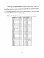
NI PXI-2503
Multiplexer
(NI TB 2605)
NI PXI-4070
DMM
Banana double
Voltage Lo
Voltage Hi
COMOCOMO-i-
Current Lo
Current Hi
C0M2C0M2+
Color identifier
Twisted
Black
Red
27
61
10
Black
Red white
44
Table 3.8 Interconnection between NI PXI-2565 REL 1 and bench board
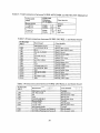
NI PXI-2565
RELl
Bench board
Color identifier
CHO
CHI
CH2
CH3
CH4
CH5
CH6
CH7
CHS
CH9
CHIO
CHll
CH12
CH13
CH14
CH15
Mini banana double
lA VINXA & RIA
RIA
R2A&3AR1AX
3A
3A VOA&CIA
R3A
4A -INA & R4A
4A
C2A
7A-GND & R5A-J1
1BVINXB& RIB
RIB
R2B & 3B RlBX
3B
3BV0B&C1B
R3B
Twisted
Black & blue marine
Black & blue marine white
Black & brown
Black & brown white
Black & gray
Black & gray white
Black & green
Black & green white
Black & orange
Black & orange white
Black & purple
Black & purple white
Black & white
Black & black white
Black & yellow
Black & yellow white
Table 3.9 Interconnection between NI PXI-2565 Relay 2 and bench board
NI PXI-2565
REL 2
CHO
CHI
CH2
CH3
CH4
CH5
CH6
CH7
Benchboard
_ '. -
Mini banana double
4B -INB & R4B
4B
C2B
7B GND & R5B-J2
Banana double
+VS & +VSX
-VS &-VSX
Mini banana double
2A VXA & Floating mini banana A
2B VXB & Floating mini banana B
39
Color identifier
Twisted
Blue & brown
Blue & brown white
Blue & gray
Blue & gray white
Twisted
Blue & green
Blue & green white
Twisted
Blue & piuple
Blue & purple white
'\
It is important to notice that polarity is not necessary when connecting the relay
modules to the bench board because each channel represents the two terminals of a relay.
Table 3.10 Interconnection between NI PXI-2503 Multiplexer and bench board
NI PXI-2503
MUX
through NI TB 2605
voltage measurements
Bench board
Color identifier
Mini banana double
lAGND
lA VINXA
IB GND
IB VINXB
Banana double
GND
+VSX
Twisted
Pink
Blue marine
Pink
Blue marine white
Twisted
Pink
Brown
CHOCHO-iCHlCH1 +
33
67
32
66
CH2CH2+
31
65
CH3CH3+
30
64
GND
-VSX
Pink
Brown white
CH4CH4+
CH5CH5-ICH6CH6+
29
63
28
62
25
59
Mini banana double
2AGND
Floating mini banana A
2BGND
Floating mini banana B
7AGND
7AV0A
Twisted
Pink
Gray
Pink
Gray white
Pink
Green
CH7CH7+
24
7BGND
7BV0B
Pink
Green white
6A+VS
6AVOA
6B-HVS
6BV0B
5A-VS
5AVOA
5B-VS
5BV0B
Pink
Orange
Pink
Orange white
Pink
Purple
Pink
Purple white
Banana double
-i-VS
+VSX
-VSX
Twisted
Pink
White
Pink
Black white
Twisted
Pink
Yellow
Pink
Yellow white
CH8CH8-ICH9CH9+
CHIOCHIO-H
CHllCH11 +
Current
58
23
57
21
55
20
54
19
53
measurements
CH12CH12+
CH13CH13+
16
50
15
49
CH14CH14-ICH15CH15+
14
48
13
47
-vs
Mini banana double
7AGND
7AV0A
7BGND
7BV0B
40
Table 3.11 Interconnection between NI PXI-6704 Analog output and bench board
NI PXI-6704
Analog output
(NI TB 2605)
Voltage supply
Bench board
Color identifier
AGNDO
VCHO
AGNDl
VCHl
Voltage supply
68
34
33
66
Mini banana double
lAGND
lA VINXA
IB GND
IB VINXB
Twisted
Pink
Red
Pink
Red white
Banana single
Single
VCH2
31
-t-VSX
Red
VCH3
63
-VSX
White
AGND
65
GND
Black
3.4.1 HPDMMs
The HP-3458A achieves a very high resolution of 8'/2 digits with a reading rate of
100,000 readings/s. Employed for production and bench test, this is the most common
DMM used to calibrate DMMs with lower resolution. The HP-34401A is a DMM with
6V2 digits of resolution. Both HP DMMs can be controlled with GPIB commands. A
calibrated HP-34401 A DMM is used to verify that the NI PXI-4070 remains calibrated
[12,13].
Table 3.12 Interconnection between NI PXI-4070 DMM and HP-34401 A DMM
NI PXI-4070
*'^'^'^ HP-34401A
DMM
DMM
Banana double
Banana double
Voltage Lo
Voltage Lo
Voltage Hi
Voltage Hi
41
Color identifier
Twisted
Black
Red
' '*
CHAPTER 4
TEST SOFTWARE
4.1 Test program based on LabVIEW
LabVIEW is a graphical programming language based on icons instead of text to
develop applications. Data flowing from icon to icon determine the program sequence.
On the other hand text-based programming uses lines of instructions to perform execution
[19].
Two windows called Front Panel (FP) and Control Diagram (CD) are used to
create programs in LabVIEW. Controls and indicators present in the front panel serve to
input and output data. The front panel is the user interface. The control panel contains the
representation, manipulation and interconnection of these controls and indicators [19].
For example, if two controls and one indicator are created on the front panel, their
representations are also on the control diagram. Any mathematical manipulation of the
two controls can be performed only in the control diagram. When connecting the addition
of the two inputs to the output in the control diagram it is possible to see the result in the
indicator of the front panel [19].
A program created in LabVIEW is called a Virtual Instmment (VI). Any VI
inserted in another VI is named a subVI. The icon representing a subVI placed in the
control diagram of a VI can have input and output terminals around its perimeter for
interconnection [19].
The most typical way to sequence sub Vis is with the use of input and output error
terminals located on the left and right side of the subVI icon. A missing connection can
cause an error out message from a subVI. The error will pass through all subsequent
sub Vis connected unless an error detection subVI stops execution [19].
42
4.2 Test program subVIs
Since every user-created subVI has an error in control and error out indicator, as
shown in Figure 4.1, they are not included when presenting the corresponding front panel
in order to save pnnting area. Built-in LabVIEW sub Vis are only mentioned when
present in user-created sub Vis. Documentation of all the sub Vis not explained in this
chapter can be found in the help menu of the LabVIEW software.
erroi in (no ectoi)
dalus
-'J
source
-i;='o
SB^H
etrof out
code
status
m
M
code
£0
^urce
1
4
J
Figure 4.1 Error in control and error out indicator
4.2.1 Delav(mS) subVI
The Delay (mS) subVI introduces a pause in milliseconds during the transition of
the program. It has an input named "Delay(mS)". Its icon, FP and CD are shown Figure
4.2.
Delay (rnSlI
L'-'-' t""""
ir^jr^'
DelajJ
(mSJ
;-;;U.LiiJ
Delay (mS)
,Q
iJ£-=i-" 1
IL^^-;
"»" "° 1
error in (no error)
error out
Figure 4.2 Delay subVI icon, FP and CD
4.2.2 NI AO subVI
The NI AO subVI sets a voltage level in a specific channel of the NI-PXI 6704
analog output. U has two inputs called "Channel" and "Voltage". Us icon, FP and CD are
shown in Figure 4.3.
43
Channel
ikij
F' ' '
^^oUape
«ME PT
Channel
NI
AO
O.GO
error in ( n o error'
,,^^1^
error o u t
»^SI3
Figure 4.3 NI AO subVI icon, FP and CD
4.2.3 NI DMM I subVI
The NI DMM I subVI configures the NI PXI-4070 DMM to measure dc current
with a range/resolution of 20mA/10nA. It has one output named "Current". Figure 4.4
shows its icon, FP and CD.
NI PXI-4070 DMM CurentI k DC Current^ [Current
fmol^ '^Iffij
|DAQ::2::IN5TR|
[Hl-fDei^
(mS)
NI
DMM
^0.00
Current
MIDMM
^ i l
Oaiiig
:^=
error in n o error
On H
!20.0mi
error out
Figure 4.4 NI DMM I subVI icon, FP and CD
4.2.4 NI DMM V subVI
The NI DMM V subVI reads the measurement from the NI PXI-4070 DMM
previously configured for dc voltage with auto range/resolution. It has one output named
"Volts". Examine Figure 4.5 for its icon, FP and CD.
1"1511 ^ |DAQ::2::INSTR
i
If^ri™
HI
DMM
*
!.16m „MS
&elay
(mS)
•
error in (no erro )
•niDMM
;.t<HK
IPtlE3i:|
_,•!?::, v/oM
— .••SI
1
—
error out
V
Figure 4.5 NI DMM V subVI icon, FP and CD
44
4.2.5 HP DMM V subVI
The HP DMM V subVl configures the HP-34401A DMM to measure DC voltage
with a range of lOV. U has one output named "Volts". Figure 4.6 shows its icon, FP and
CD.
../oils
|^GPIB1::22::INSTRH H
EIHMay
(mS)
HP]
DMM
error in (no errorll
VISA
CLR
viSA{7].~visai~WIMI
|MEA5:V0LT:DC? 10
• n,-
1
*..,
©••-.»
'i'?i
error out
Figure 4.6 HP DMM V subVI icon, FP and CD
4.2.6 In-out equ subVI
The In-out equ subVI calculates the input-output voltage equation for the
summing junction configuration with Vs+ and Vs. at a specific potential. Figure 4.7
shows its icon, FP and CD.
The frame 0 of the Sequence Structure (SS) (Figure 4.7 CD 00 00) has a while
loop where an input voltage global variable (GV) "Vinx" is applied with the NI AO
subVI and the output voltage is measure with the NI DMM V subVI. If the output is
larger than "Desired output" GV, "Increment" GV is subtracted from "Vinx" GV,
otherwise added. "Increment" GV is divided by 2. When the output voltage is either
below Vs+ or above Vs. by 0.25V for both iterations of the For loop without surpassing
iteration 15 of the while loop, the frame 0 of the SS ends. In the frame 1 of the SS (Figure
4.7 CD 01 00) coordinates (X1,Y1) and (X2,Y2) are used to calculate the slope of the
input-output voltage equation.
Depending on the "AO channel" input value, the NI AO subVI applies the input
voltage "Vinx" GV to either op amp A or B. Global variables (GV) initialized previously
are "Vinx" at 0 and "Incremenf at 5. "Desired output" is always at the middle level of
the supplies. "Limit" defines the ±range from the "Desired output" in which the output
must be in order to store in-range coordinates (XI,Yl) and (X2,Y2). XI and X2 are input
voltages. Yl and Y2 are output voltages. "Limit" is always VS/2-0.25. "Cycle flag" GV
45
outputs 0 only if the while loop surpasses 15 iterations, otherwise it outputs I.
"Slope"=(Y2-Yl)/(X2-Xl) outputs the slope of the equation.
onnaDDODoaaDDDadfldHdlLlom
-[i ...LB d a d a p D O D d a d d d a d a d o d t
\2\-m
M-^^
[2j-J^-
•inciernenl M
:s>
ylk y—' |15
iLimitl
UHlv
dj-^
|AQ chanrieil
rl>-:-g>
r
SwT
jCyicle flaqi I
i\>>m
• incrernerif
iDesired ou^putl
iDDODODDaDaaDDDDOODDDaaQDOOQaDaQaaoQQaonaaoDOD.DD
J>>ii; I leirot out|
r^-* 1
1
i
,r^««™«|
r^<2] «>''2 i
nil
'
i
i
Figure 4.7 In-out equ subVI icon, FP and CD 00 00, CD 00 01 and CD 01 00
By substituting any desired output voltage Y in Equation 4.1 its corresponding
input voltage X can be calculated. The slope along with any pair of coordinates (XI,Yl)
or (X2,Y2) acquired from the In-out equ subVI are needed for the calculation.
46
X = (Y-Yl)/Slope-Xl
Equation 4.1
4.2.7 Set out 1 subVI
Based on an initial input voltage "Vinx" GV calculated with the input-output
voltage equation from in-out eq subVI, the Set out 1 subVI moves the output at a desired
voltage level by adjusting the input with "Increment" GV having Vs+ and Vs. at a specific
potential. Icon, FP and CD for this subVI are shown in Figure 4.8.
rchanriet
Desired output ]
Vout
Set
out 1
Cycle flag
I
VQUII I l i l D
• Error
Vinxl |roBr;>l- (#Vin:.
-?i>
m
r^^>-j[¥lncternent.
1^0 channeil
KMi •—F
l^~
l~
[error inlnoerrorjj [TST
i t g ^ l [error out]
Figure 4.8 Set out 1 subVI icon, FP and CD
4.2.8 Set out 2 subVI
Only if the Set out 1 subVI surpasses 15 iterations, the Set out 2 subVI changes
the output to a desired voltage level starting with an initial voltage "Vinx" GV of OV and
an "Increment" GV of 5V. Otherwise the Set out 2 subVI passes "Vout" and "Cycle flag"
coming from the Set out 1 subVI. Refer to Figure 4.9 for its icon, FP and CD.
47
riom
Voutprev
.aai
Cycle flag prev
[Jo
**" AO channel
Set
out 2
'Jcioo
1275^'"'
SMI
Desired output
Vout
Cycle flag
False •^
• incre^menl j i ' C ^ ""- .^
K'out prev]
:*ir
' U H l Increrriei'i!
-[astJi fvoud
fraBTH—
-^B>T-^,
Ht^
;lv> g!
IDesired output!
NI
AO
rji
DMM
V
Figure 4.9 Set out 2 subVI icon, FP, CD 00 00 and CD 01 00
48
[Cycle (lag]
4.3 Test Seq suhVl
The Test Seq subVI is in charge of testing all DC parameters, writing the results
to a *.csv test file, and output the results and pass/fail flags. This is the most important
subVI. Global variables (GV) needed for this subVI are previously initialized in the Test
program VI. Refer to Figure 4.10 for its icon and FP.
:fQuiesent cunent
• Input bias current A
-Input bias current A
Input offset current A
+ Input bias current B
• Input bias current B
Input offset current B
Input offset voltage A
Input offset voltage B
PSRR A
PSRR 8
CMRR A half
CMRR A fuB
CMRR B half
CMRR B full
Open loop gain A
Open loop gaji B
+ Swing A
•SwingA
Test
Seq
+SwiigB
- Swing B
Figure 4.10 Test Seq subVI icon and FP
4.3.1 In measurement Test Seq subVI CD 00 00
The Test Seq subVI CD 00 00 shown in Figure 4.11 performs the quiescent
current measurement. The GV "N" indicates that the Test Seq subVI is repeated N times.
49
ET
i| 010 61 - k P a B P a g a a B P P . n 0 D n 0 H a H P B B H B B H a H g a B H g H g
IQUIESCENT CURRENT MEASUREMENT!
INI F»3 2565 RdJTTI INI t^-2565 ReliTH I"' ^ 1 ^ 3 Hu»l
|PXI?9IN';TH'
E
[T] ii^i.iiiNSTRi I
r j F X I l 11 INS'lfll
jm
n]
Jo
|F^<I2 15 INSTRl
1 ^
|RKI2,15, INSTRI
|CH2j|CH12l
|CH2]
( c p
I^'^
INI PXI-2565 Relay 21 [NTSaZSSS Relai' 11
^ "^^^"1
|CHir]
"a ^a "a "a ^a
^a
IcoMllOoMllImMilUmMlllraMll
|cte]
IPXI215 INSTRI
•
!
|CH4]
S ] *;»
^ ^
Ep)
^H
| ^
r l P ^ i 11 IHSTRI
[cHSl
^H
tcOMg]
|"DCyc<s - I
<2J l-^.«1^i^JHMl»l
Figure 4.11 Quiescent current measurement Test Seq subVI CD 00 00
RELI, REL2 and MUX relays are open. The two inputs of op amp A and B are
set to zero. The power supplies are applied based on the corresponding two values for this
test selected from the GV vectors "-i-VSs" and "-VSs". REL1CH8, REL1CH2,
REL1CH12, REL2CH2 and REL2CH5 are closed to have the voltage follower circuit
shown in Figure 2.9. MUXCH12 relay is then closed to measure IQ with the NI DMM I
subVI and then the result is stored in "IQ" GV. REL2CH4, REL2CH3, and REL1CH9
are closed to connect VCH2 (Vs+) and R5. Finally the NI PXI 4070 is configured to
measure voltage with autorange.
4.3.2 In^ A measurement Test Seq subVI CD 01 00
The Test Seq suvVI CD 01 00 shown in Figure 4.12 performs the positive input
bias current measurement of op amp A.
The power supplies are applied based on the corresponding two values for this
test selected from the GV vectors "-i-VSs" and "-VSs". All the relays of the MUX are
open. MUXCH6 is closed to allow measuring the output of op amp A. REL1CH8 is open
50
to start the current integration with C2A based on the stop watch integration circuit
shown in Figure 2.10. A delay indicated by "IB Delta start" GV is introduced before
taking the first output reading for settling. Another delay "IB Delta I" is used before
taking the second output reading. IB+ for op amp A is calculated by taking the difference
of the two output readings multiplied by "IB CAP"/"IB delta t". The result is then stored
in "+IB A" GV. The integration status flag "IB Vout flag" is utilized to monitor the
output of op amp A with the Test program VI.
|t INPUT BIAS CURRENfAl
|NIR-<l-2503Mux| |NI PXI-2565 R 5 ^
|PXI2:9:INSTR|
•tie A
|R<n::11::INSTR"
i>r^-^
Figure 4.12 Positive input bias current measurement A Test Seq subVI CD 01 00
4.3.3 Ii^. A measurement Test Seq subVI CD 01 01
The Test Seq suvVI CD 01 01 shown in Figure 4.13 performs the negative input
bias current measurement of op amp A and calculates IQSA-
•INPUT BIAS CURRENT A
bE:3~^ ^
lfirR<l-2565Relav1|
^^\^
R><I1::11::INSTR|
|CH5|
IciH8
Delay
(mS)
•Eg
CGM5| ICOMS
-
Im
®-iBA!l
[CHI
HlSutch
IC0M4
'IB Vout feg
NI
OMM
Delay
(mS)
X
|C0M2|
fToool
h^'t' i> •:\iaJa'^
OMM
^1
•lOS
I
^
[TOM]
fc>
• I statu: [ me Voul tl-ag
|#iBM.5'ri{-L-
Figure 4.13 Negative input bias current measurement A Test Seq subVI CD 01 01
51
REL1CH4, REL1CH5 and REL1CH8 are closed to have the test circuit shown in
Figure 2.11. REL1CH2 is open to start the cunent integration with CIA. A delay
indicated by "IB Delta start" GV is introduced before taking the first output reading for
settling. Another delay "IB Delta I" is used before taking the second output reading. IBfor op amp A is calculated by taking the inverse difference of the two output readings
multiplied by "IB CAFTTB delta I". The result is then stored in "-IB A" GV. IQSA is
calculated and stored in "lOS A". The integration status flag "IB Vout flag" is utilized to
monitor the output of op amp A with the Test program VI.
4.3.4 IR^ B measurement Test Seq subVI CD 01 02
The Test Seq suvVI CD 01 02 shown in Figure 4.14 performs the positive input
bias current measurement of op amp B.
•INPUT BIAS CURRENTS
INI FXI-2565 Relav 11 |NI PXI-2503 Mu«| JNI PXI-2565 Relay 2|
iPXI1.:11::INSTR| RKI2:9::INSTR1 |FXI2::15::INSTR| j
^ ^ ' '
'
^ ^ 1 '
^
CHT
! # ^ G [ i e ! t a jtsU
Figure 4.14 Positive input bias current measurement B Test Seq subVI CD 01 02
RELICH2 is closed and REL1CH4 is open to have the test circuit shown in
Figure 2.10. All the relays of the MUX are open. MUXCH7 is closed to allow measuring
the output of op amp B. REL2CH2 is open to start the current integration with C2B. A
delay indicated by "IB Delta start" GV is introduced before taking the first output reading
for settiing. Another delay "IB Delta t" is used before taking the second output reading.
IB+ for op amp B is calculated by taking the difference of the two output readings
multiplied by "IB CAP"/"IB delta t". The result is then stored in "-i-IB B" GV. The
52
integration status flag "IB Vout flag" is utilized to monitor the output of op amp B with
the Test program VI.
4.3.5 IR. B measurement Test Seq subVI CD 01 03
The Test Seq suvVI CD 01 03 shown in Figure 4.15 performs the negative input
bias current measurement of op amp B and calculates IQSB-
[NI PXI-2565 Relav 21
iFXI2.15::INSTR|
|NIFXI^2565R'eiiHl
INI PXI-2565 Relav 11
rlPXn .n:.INSTR|
|PXI1::11::INSTR|
fciil
ml 7«=s
|CQM14|fcOMT5]
|^5M71
•INPUT BIAS CURRENTS
°+*l^'^m:-| "O
^IB Vout (la
ji»lll-^
"-7^^-
I [am]
Delaji
(mS)
NI
[iMM
Delay
J(mSl
||»-'3B!I
i # ' i . LjiP
i|B Jtatus
il^0MT2 |
l®ICr
EM—[x>-i EM]—3>• IB r.iflla -(art
Ml
'IB Voul flag
»IB'[iplta'i|-'-
Figure 4.15 Negative input bias current measurement B Test Seq subVI CD 01 03
REL1CH14, REL1CH15 and REL2CH2 are closed to have the test circuit shown
in Figure 2.11. REL1CH12 is open to start the current integration with CIB. A delay
indicated by "IB Delta start" GV is introduced before taking the first output reading for
settiing. Another delay "IB Delta t" is used before taking the second output reading. IBfor op amp B is calculated by taking the inverse difference of the two output readings
multiplied by "IB CAP"/"IB delta t". The result is then stored in "-IB B" GV. IQSB is
calculated and stored in "lOS B". The integration status flag "IB Vout flag" is utilized to
monitor the output of op amp B with the Test program VI. The "IB status" GV serves to
stop monitoring the output in the Test program VI.
53
4.3.6 Summing junction configuration set up Test Sep subVI CD 02 00
The Test Seq subVI CD 02 00 shown in Figure 4.16 closes REL1CH12, opens
REL1CH14, REL1CH5 and RELICH15, closes REL1CH6, opens RELICH9, closes
REL2CH0, REL2CH6 and REL2CH7, opens REL2CH3 and closes RELICHO and
RELICHIO in order to have the Summing junction configuration.
SUMMING JUNCTION CONFIGURATION
INI PXI-2565 RelaHl
Ep]
|NI PXI^2565 Relay 11
INI PXI-2565 Relav 2|
Ipxiin INSTR]
H R < I 2 : 1 5 : INSTRl
[CHUl |CH5
rem?) |CHr][CH9
EHD
n
|FXI1::11::INSTR|
ICHT] [CH7
MISut-:h
EHU
NlSLJ»<:h
{CHIO I
[ICHOI ICHIO
t~*ISuti
wn
?S
|C0M12|fEgMT4]|gfe roMi[5j|coM6|fcoM3] | g ^ [^5M!I j r o ^ i^SMT] ITOM^ [COMIOI
•+,
Figure 4.16 Summing junction configuration set up Test Seq subVI CD 02 00
4.3.7 Vin vector Test Seq subVI CD 03 Ox
The Test Seq subVI CD 03 Ox shown in Figure 4.17 generates the Vin vector used
to have initial input voltages when measuring the parameters with the Surmning junction
configuration.
The two iterations of the first For loop are used to determine whether op amp A or
B is being tested by selecting the output MUXCH6 or MUXCH7 to be measured and the
input VHO or VHCl to be applied with the In-Out equ subVI and the sequence the "Cycle
flags" binary vector GV values are stored.
The eight iterations of the second For loop are used to select the power supplies
level, store in "Vin vector" GV the calculated input voltages required to set the output of
the op amp A and B at a specific voltage level, change the desired output for the AQL
inputs calculation when iterations 6 and 7 are present, and sequence the "Cycle flags"
binary vector GV values storage.
For every iteration of the second For loop, the inputs and power supplies of the op
amp A and B are set to zero. Then the power supplies are set based on the values selected
per iteration from the global variables "-i-VSs" and "-VSs". The middle point of the
54
supplies and Vs/2-0.25 are input to the In-Out equ subVI. The In-Out equ subVI outputs
the in-out equation values: slope, input ("XI" GV) and output ("Yl" GV). The Case
stmcture passes the desired output in order to calculate its corresponding input based on
the in-out equation values. This desired output is always at the middle point of the
supplies except for iterations 6 and 7; corresponding to the open loop gain (AQL)
calculation. The "Cycle flags" binary vector GV stores flags to indicate for which
iteration the In-Out equ subVI surpassed 15 iterations.
<|Tiue
-K
^
feoJT«^.»<
Figure 4.17 Vin vector Test Seq subVI CD 04 00 and CD 03 01
4.3.8 Parameters with Summing Junction Test Seq subVI CD 04 Ox
The Test Seq subVI CD 04 Ox shown in Figure 4.18 and Figure 4.19 calculates
the parameters related to the Summing junction configuration.
55
[PARAMETERS WITH SUMI^INGJIJNCTIONI
CD-
[SHNI
J f a b z n
fe:l>
I^^^^E."^
.NI
J AO
iR~:i2 9 INSTRI
INI R<l-;503 M^
ri--i
- • t o
i
[•-li
'^r
^
- • < a
V
"^
Figure 4.18 Parameters with Summing Junction Test Seq subVI CD 04 00
The two iterations of the first For loop are used to determine whether op amp A or
B is being tested by selecting the output MUXCH6 or MUXCH7 to be measured and the
input VCHO or VCHl to be applied with the Set out 1 subVI and Set out 2 subVI, the
calculation to be performed with the Sequence structure, the input MUX4 or MUX5 to
be measured and the sequence the "Cycle flags" binary vector GV values are stored.
The eight iterations of the second For loop are used to select the power supplies
level, the calculation to be performed with the Sequence structure and the input voltage
from the "Vin vector" GV, change the desired output for the AQL calculation when
iterations 6 and 7 are present and sequence the "Cycle flags" binary vector GV values
storage.
For every iteration of the second For loop, the inputs and power supplies of the op
amp A and B are set to zero. Then the power supplies are set based on the values selected
per iteration from the global variables "-i-VSs" and "-VSs". The middle point of the
supplies is always input to the Set out 1 and Set out 2 sub Vis except for iterations 6 and
7; corresponding to the open loop gain (AQL) calculation.
56
Only if the Set out 1 subVl cannot put the op amp's output to the desired voltage
when it surpasses 15 iterations, the Set out 2 subVI is executed. The measured desired
output is input to the Sequence structure. Once the desired output is reached, VXA or
VXB, depending on the op amp being tested with MUXCH4 or MUXCH5 respectively,
is measured and the voltage between the two inputs of the op amp is calculated.
N'™™™™nH2 - ^ • " " ' " ™
I
jPSRRAV^ll
_ » >|5 .|.r««»-»"
|CMRRA'/53I
^
It--' 1
. [>
^
IPSRHAVS2I
1
*
'
ft*' '^M
} 9
L* '^'
^3 1
nZET|tOLAVS2l
iPSRRBVS2|
iM
HI»Vr.A
(•FShir^O
l&r?IEl~
JCMRRBVSII
p!^
Figure 4.19 Parameters with Summing Junction Test Seq subVI CD 04 01 to CD 04 15
Calculations for every parameter are performed and stored in GVs as shown in
Figure 4.19. The "Cycle flags" binary vector GV stores flags to indicate for which
iteration the Set out 1 or Set out 2 sub Vis surpassed 15 iterations.
4.3.9 Writing results Test Seq subVI CD 05 00
The Test Seq subVI CD 05 00 shown in Figure 4.20 writes to a *.csv file the DUT
number, test temperature, pass/fail test label and results of all the calculated DC
parameters. The results and pass/fail indicator per parameter is displayed in the front
panel of the Test program.
57
IWRITING RESULTS!
Figure 4.20 Writing results Test Seq subVI CD 05 00
The test results are grouped into a vector, divided by their units, compared to
"Limits max" and "Limits min" GVs to obtain the pass/fail test label, grouped again with
the DUT number ("DUT" GV) and the test temperature ("Temp" GV) and then written to
a *.csv file specified by the "Path" GV. The "Cycle flags" binary vector GV is
reorganized to match the test results order in order to indicate in the control panel of the
Test program which parameter passed or failed.
4.4 Test Program VI
The Test Program VI performs the verification routine, initializes the global
variables required for the entire test, writes to a *.csv file the labels of the DC test results
and controls the Test Seq subVI. This VI provides the main user interface. Refer to
Figure 4.21 and Figure 4.22 for the control panels (CP) of the Test program and the
Verification routine.
58
E>^ Dual fipa lett piog.vi'
Figure 4.21 Test Program CP 00 00
The Test Program CP 00 00 shown in Figure 4.21 serves to input the "DUT"
number, the "Path" and name of the *.csv file, the "Product" to be tested, the number of
times "#Iterations" to test the DUT and the parameters used to perform the bias current
measurement: "IB CAP", "IB Delta start" and "IB Delta t". This CP also displays the
"Test time (sec)", the output voltage of the op amp being tested when the bias current
measurement is performed, the test pass/fail flags per parameter, the name of the
parameters, the test results and the test limits.
The Test Program CP 00 01 shown in Figure 4.22 displays the results of the
Verification routine.
In the left side of this CP, the difference between the NI DMM and the HP DMM
readmgs are shown graphically and numencally. The "PASS/FAIL CORRELATION"
59
flag changes to red every time the NI DMM HP DMM difference surpasses 350/xV. The
voltage being measured by the NI DMM is numerically displayed.
In the right side of this CP, the difference between the ideal voltages applied by
the AO and the NI DMM readings are shown graphically and numerically. The
"PASS/FAIL CORRELATION" flag changes to red every time the AO - HP DMM
difference surpasses 350ju.V. The voltage being measured by the HP DMM is numerically
displayed.
Test ptogram
Vetiftcalion louti
Delta (AO-HP DMM)
Delta(NIDMM^HPDMM)
Figure 4.22 Test Program CP 00 01
Before this VI is running the Verification routine tab has to be hit in order for the
Verification routine to be executed. Otherwise the Test program starts and once it
happens the only variables that can be changed are: "DUT" number, "Path" and
"#Iterations".
60
4.4.1 Verification routine Test Program VI CD 00 00
The Test Program VI CD 00 00 shown in Figure 4.23 performs the verification
routine only if "Tab" selects the "Verification routine" state of the case structure. The
other sate is empty.
I.J.IHII.I.UUII.II.I.|lJliWB
File &dt Qpfliate loots
Qrowte Jf/indow
Ijelp
'3
n n n n n n n n n n n n n n n n p ' n n n n n n n n i u i 4 . | QIQ j i . ^ p n n n B n a f l o c n D n f l g o n a a a o o a a
aTrun
Figure 4.23 Verification routine Test Program VI CD 00 00
The NI DMM is configured to measure in autorange. The four iterations of the
first For loop are used to select the places (VCHO, VCHl, VCH2 and VCH3) where the
voltages are applied with the NI AO subVI and measured (MUXO, MUX3, MUX6 and
MUX7) with the NI DMM and the HP DMM. The three iterations of the second For loop
are used to set three voltages (-5, 0 and 5) with the NI AO subVI per every iteration of
the first For loop.
61
For every iteration of the second For loop the NI AO subVI applies a voltage , all
relays are open, the MUX is selected, readings from the NI DMM V subVI and the HP
DMM V subVI are taken and displayed in the control panel, the difference between the
NI DMM V subVI reading and the HP DMM V subVI reading is displayed in the left
side of the control panel, the difference between the voltage applied and the HP DMM V
subVI reading is displayed in the right side of the control panel, and the pass/fail
correlation flags are changed to red in the control panel if their corresponding difference
is more than 350jLtV.
4.4.2 Variables initialization Test Program VI CD 01 Ox
The Test Program VI CD 01 Ox shown in Figure 4.24 and Figure 4.25 initializes
the variables required to perform the test and identify with labels the results written to a
*.csv file. The "Product" control allows initiaUzing variables for dual op amps with
different test conditions.
attaot]dQadO&aDdddadoBad&aadBB[|,|l[0
3] T^p' a O O D D O D a a D D D D D D D D D O o o O D D a i
PDDODDdnnnnnDounnnnnuUL.r,r.nhDUunnapaaDMaooqo"L,udDODQDqadDnaDDDD
Figure 4.24 Variables initialization Test Program VI CD 01 00
62
The Test Program VI CD 01 00 shown in Figure 4.24 initializes the "#Iterations"
GV used to test the DUT N times in the Test Seq subVI, the GVs required for the input
bias current measurement, the resistor values of the Summing junction configuration, the
"Error" GV utilized to guard band the desired output, the test temperature "Temp" GV,
the "AOL dV" GV used to set the output with respect to the supplies when measuring
AoL, the product identifier "Product" GV and the results units labels "Units labels" GV
vector.
HI 110 4 | ^ H " " " » » ° " ^ " " ^
i| 210 41 -k-Ml." "hnnn
nrrm
E3M
EiEEEl
(13M
fji
it
Ei-
m—
Q'ft'fl'tiBQt3'ta'ti'B"D'taanaa'cta^rytia'annbtiatidi
i H a a B a n o a'B-a-HTM>'T™'gH-fftni a-ga PH'HTrtl
ij4[0
310 41 ^HJiJi n B n a n oicnrHj T
4]^^BaaaaaaaaB"g
I*V51| ;27fi
IIQWS1I [275]
IVOStVSII i j T J —
IPSRR.VSII
33-
IPSRR »vs:l iTs]
[CMRR.VSII g y }
ICMRR WS2I n 7 |
iCMRRW53l ijjj
IA0LWS1I .[275}lAOL WS2I [275]
V-
!::_;_ [>
(vsj
liTvsTI
IVOS -VS11
IPSRR-VSlI
K R R -VS2I
«
'•-2 75!
lii]— 112 t23 •
ICMRR-VSII
ICMRR -VS2I
ICMRR -V53I
lAOL-VSIl
IA0L-VS2I
I'rtHBaaartnnftrittHrtHrtrttiHrtaililLJoauui
i. n
h5 7]- -
m
n n H B a a H B a '••iM—
a a a n n n n a a B B a H a o BTral
Figure 4.25 Variables initialization Test Program VI CD 01 01 to CD 01 04
63
The Test Program VI CD 01 01 to CD 01 04 shown in Figure 4.25 initializes the
results units "Units numbers" GV vector used to present the results in terms of their units,
the minimum "Limits min" GV vector and maximum "Limits max" GV vector limits
used to know if the DUT passed or failed, the power supplies levels per test "+VSs" GV
vector and "-VSs" GV vector, the power supplies change "PSRR dVS" needed for the
PSRR measurement, the common mode voltage change "CMRR dCMl" used for the
CMRR half scale measurement and the common mode voltage change "CMRR dCM2"
used for the CMRR full scale measurement
4.4.3 Writing labels Test Program VI CD 02 Ox
The Test Program VI CD 02 Ox shown in Figure 4.26 is used to write to a *.csv
file the labels required to identify the product name, date, serialization, temperature,
pass/fail status, parameters results, units, limits min and limits max of the devices under
test. The Test Program VI CD 02 01 also displays in the CP the parameters labels.
iDUTIIt-
[[ffjKDNhS^-
I Write units labels I
1
© I J n i l - label: [|_
J-ESt-L.
IlimilsMinl
r-,
IWrite limits mini
1
lp3D
'-|a- HI 1|IS3„
CHa::
a
j^P^l^jHfES)^
m
mn .Ma
|LirriiU Max [
1^1
|Write limits maxl
MED
1
'1^
ten
Figure 4.26 Writing labels Test Program VI CD 02 00 to CD 02 04
64
H
labc. 1
Every diagram shown in Figure 4.26 indicates one row to be written in the *.csv
file. The order in which these rows are written is shown below.
"Product" GV and date
"DUT#", "TEMP", "PASS/FAIL" and parameters labels
"Units labels" GV
"Limits min" GV
"Limits max" GV
4.4.4 Test Program VI CD 03 Ox
The Test Program VI CD 03 Ox shown in Figure 4.27 controls the Test Seq
subVI.
In the first Sequence stmcture the "IB status" flag is set to "tme" and the "Test
status" flag is set to "false" to indicate in the CP with a green color around the 'Test"
button control that the DC test can be started. Before hitting the "Test" button control the
user can change the "DUT" number in the CP.
ID10 21 'M o g B g LCg
1 o q o q q<| 1 [Q 2| -r^f Q n • a p o T
l"e''^'"l
a d a 00014,1 210 21-kF'^ B a d d n t
IO~l|Te.l.ak.:i)
-[«TF)
•n<|True
-ff'
^ .
IPAQ 2 IHSTRI
l^^^g
I5~l
CD
\\»IE i!atu;|
DDQonnnaaaaDDnnDaoSt:
m
cmm
|l»IB-lji«i| E>1
' Q o a B i 3 q q H o d a a B B & b q"g~o~a
m
cai n ;
iOoabdannata'aaaaaaaBfllS
m
%«cKmsiaeK««3%»s£%a»£$s;<K!ai
Figure 4.27 Test Program VI CD 03 00 to CD 03 02
Once the "Test" button control is hit the second Sequence structure starts
initializing the "Test status" GV to "true" to indicate in the CP with a red color around
the "Test" button control that the DC test is running. The "Test time" GV stores the
65
current counter. The Test Seq subVl starts and the output of the op amp in use is
displayed in the CP when the "IB Vout flag" G V changes to "true" during the IB
measurement. After completion of the Test Seq subVI the test results and the pass/fail
flags per test are displayed in the CP.
In the third Sequence structure the test time is shown in the CP based on the
difference of the current and previous counter values.
The Sequence structure will be running until the stop button in the main menu of
the control panel is hit.
66
CHAPTER 5
DATA ANALYSIS FOR REPEATABILITY AND CORRELATION
Once a test system is working, a statistical data analysis of the test results is
required to determine its performance. Measuring the same guardbanded value for a
specific parameter every time the DUT is tested does not mean the reading is accurate but
repeatable for the test system being used. The measurements may vary from system to
system and the task of a test engineer is to determine which system is right by doing
readings by hand [2].
In this chapter, an Automated Test Equipment (ATE) system already approved is
used to compare the results of the Automated Bench Test Equipment (ABE).
Repeatability and accuracy depend on the test instmments characteristics, the expected
measurement, maximum (upper test limit UTL) and minimum (lower test limit) test
limits, noise and the test circuit design.
The minimum number of samples required to have a normal distribution is 30.
The results taken from one device tested 35 times serve to obtain the repeatability of each
system. Thirty five devices tested on both systems are used for correlation analysis.
The per-parameter repeatability criterion shown below assures that a device can
be tested repeatedly in the ABE without surpassing the test limits.
•
M-ABE + BOABE + 6OABE _R <
UTL
•
l^ABE - 3 0 A B E - 6aABE_R > L T L
where
PABE is
the mean of the 35 devices tested at the ABE
OABE is
the standard deviation of the 35 devices tested at the ABE
CJABE_R is
the standard deviation of the same device tested 35 times at the ABE.
The ABE is considered repeatable for a specific parameter if meeting at least the
last two repeatability conditions shown below.
•
OABE _R — CJATE _R
•
6aABE R<3%of(UTL-LTL)
67
•
PABE + 3OABE + 6OABE _ K < UTL
•
I^ABE
3OABE - 6OABE_R > LTL.
If the second repeatabihty condition is met, the parameter can be used to
determine if the system's repeatability has changed every time a test is perform.
The per-parameter correlation criterion shown below assures that the same device
can be tested at the ATE and the ABE without surpassing the test limits.
•
I^ABE +
3aABE + l^icl + 3ac < UTL
•
ItABE - 3OABE
IPCI
- 3ac > LTL
where
Pc is the mean of the ATE and ABE delta results of the 35 devices
oc is the standard deviation of the ATE and ABE delta results of the 35 devices.
The ABE correlates with the ATE if the three correlation conditions shown below
are met for a specific parameter.
•
IPCI
+ 3ac < 3% of (UTL-LTL)
•
PABE +
•
I^ABE 3aABE ll^cl - 3ac > LTL
3aABE + llk:| + 3ac < UTL
o^ATE _R is the standard deviation of the same device tested 35 times at the ATE
|j,ABE is the mean of the 35 devices tested at the ATE
OABE is
the standard deviation of the 35 devices tested at the ATE.
If the second repeatability condition is met, the parameter can be used to
determine if the correlation between systems has changed every time a test is perform.
The highlighted cells in the repeatability and correlation results tables indicate the
failures for that particular condition of the parameter.
5.1.1 IQ data analysis
Based on the data of Table 5.1, the IQ repeatability and correlation results are
calculated and shown in Table 5.2 and
Table 5.3. This parameter is repeatable at the ABE because the last two
repeatability conditions are met. Since the second repeatability condition is met this
68
parameter can be used to determine a change in the ABE's repeatability. All correlation
conditions are met, therefore the ABE correlates with the ATE for this parameter.
Table 5.1 IQ statistical data
(IO)MA
0,058
0.033
42-824
2.638
42.742
2.135
-0.082
0.303
23.5
63.4
OABB R
OAFI: R
^lABE
TABE
MATE
OATE
PC
Oc
LTL
UTL
Table 5.2 IQ repeatability results
Conditions
"ABE
1O(MA)
R-OATE R
6OABE R<3% (UTL-LTL)
MABE+30ABE+6aABE R < U T L
|JABE-3OABE-6OABE R>LTL
Result
0.058>0.033
0.34<1.197
50.174<63-4
34.562>23.5
pass
Table 5.3 IQ correlation results
Conditions
|Mcl+3oc<3'7f (UTL-LTL)
|JABE+3oABE+IHcl+3ac<UTL
HABE-3aABE-||Jc|-3cJc>LTL
Result
IQ (*tA)
0.99KL197
51.729<63.4
33.919>23.5
pass
5.1.2 IR data analysis
Based on the data of Table 5.4, the Is repeatability and correlation results are
calculated and shown in Table 5.5 and Table 5.6.
Since the last two repeatability conditions are met for all the IB parameters there is
confidence that a device can be tested repeatedly in the ABE without surpassing the test
limits and therefore the ABE is considered repeatable for IsEven though the ABE does not correlate with the ATE for this parameter, the
same device can be tested at the ATE and the ABE without surpassing the test limits
because the last two correlation conditions are met as shown in Table 5.6.
69
Table 5.4 IB statistical data
A)
pA
0.29
0 32
0.17
0.09
1.62
0.12
1.45
0.17
-7.8
7.8
(IB-A)
(IB.
OABE R
OATE R
PABE
"ABE
PATE
OATE
Pc
ac
LTL
UTL
pA
0.77
0.26
0.38
0.44
4.58
0.33
4.19
0.53
-7.8
7.8
A)
pA
0.93
0.41
-0.21
0.48
-2.95
0.32
-2.74
0.59
-7.8
7.8
(IDS
(Is. B)
pA
0.55
0.32
0.13
0.04
3.41
0.32
3.27
0.31
-7.8
7.8
(IB.B)
pA
0.52
0.23
0.31
0.11
5.13
0.15
4.82
0.14
-7.8
7.8
dos B)
pA
0.78
0.38
-0.18
0,11
-1.72
0.27
-1.54
0.31
-7.8
7.8
Table 5.5 IB repeatability results
Conditions
OABE R ^ O A T E
R
6aABE R<3% (UTL-LTL)
PABE+30ABE+6aABE R < U T L
PABE-3aABE-6aABE R > L T L
Results
(IB. A)
pA
;> ...-/.PA, • ..
0.29<0.32
0.77>0.26
1.74<0.23
4.6>0.23
2.19<7.8
6.32<7.8
-1.84>-7.8
-5.51>-7.8
pass
pass
dos A)
. . . , . p A .0.93>0.4I
5.61>0.23
6.85<7.8
-7.26>-7.8
pass
(W B)
pA
0.55>0,32
3.29>0.23
3.56<7.8
-3.29>-7.8
pass
(IB-B)
pA
0.52>0.23
3.13>0.23
3.76<7.8
-3.06>-7.8
pass
(lOS B)
pA
0.78>0.38
4.68>0.23
4.84<7.8
-5.14>-7.8
Pass
Table 5.6 IB correlation results
Conditions
|Hcl+3oc<5% UTL
PABE+3aABE+IPcl+3cTc<UTL
PABE-3CTABE-IPCI-3OC>LTL
Results
-:- % A)
1.966<0.39
2.417<7.8
-2.067>-7.8
fail
(liA)
Pr'MW''-^
pA :
pA . J. :
5.785<0.39
4.524<0.39
5.778<7.8
7.49<7.8
-6.192>-7.8
-6.726>-7.8
fail
fail
(IBH.B)
pA .
4.215<0.39
4.485<7.8
-4.215>-7.8
fail
(IB- B )
pA
5.23K0.39
5.864<7.8
-5.24>-7.8
fail
dos B)
pA
2.48<0.39
2.645<7.8
-2.999>-7.8
fail
Based on the means for all the IB parameters tested on the ATE, it is noticeable
that a leakage is present in the measurement. Instead of obtaining the typical value of
0.5pA for the OPA2347 on the ATE, a mean of more than 1.5pA is being measured for
all the IB parameters. On the other hand, the ABE has a leakage only for IB- A.
Under these circumstances the only way to determine if the systems are reliable
enough to detect if the IB parameters of the device surpass the test limits is by using a
device with a higher value of IB- A well-known device with a typical IB of lOpA was
used. Both systems measured the typical value with a discrepancy of 3pA.
70
5.1.3 SWnijT from rail data analysis
Since this purpose of this test is to coiroborale if the output of the op amp can
swing at least 15mV from each rail, it is considered a pass/fail test and no repeatability
and correlation study have to be performed.
In order to verify if the output can be in the range of ±2.735V to ±2.75V, the ATE
sets the output at 2.736V with a tolerance of less than ±0.5mV and the ABE sets the
output at 2.74V with a tolerance of less than ±5mV.
5.1.4 Vns data analysis
Based on the data of Table 5.7 the ABE meets all the repeatability and correlation
conditions for VQS as shown in Table 5.8 and Table 5.9. As a result the ABE is
considered repeatable and correlates with the ATE for this parameter.
Table 5.7 Vos statistical data
(Vos B)
mV
(Vos A)
mV
OABE_R
0.007
0.004
OATE _R
0.007
0.006
PABE
-0.429
-0.558
OABE
1.407
L212
PATE
-0.419
-0.561
OATE
L417
1.229
Pc
0.010
-0,003
Oc
LTL
UTL
0.098
-5.740
0.091
-5.740
5.740
5.740
Table 5.8 Vos repeatability resuhs
(Vos A)
mV
Conditions
(Vos B)
mV
0.007=0.007
0.004<0 006
6CABE R < 3 % (UTL-LTL)
0.042 <0.344
0.024<0.344
P ABE+ 3 o ABE+6OABE _ R < U T L
3.834<5.740
3.102<5.740
PABE-3OABE-6OABE_R>LTL
-4.692>-5.740 -4.218>-5.740
Results
pass
OABE R-OATE R
71
pass
Table 5.9 Vos correlation results
Conditions
(Vos A)
mV
|Pc|+3oc<3% (UTL-LTL)
(Vos B)
mV
0.304<0 344
0.27()<0 344
PABE+3aABE+IPcl+3CTc<UTL 4.096<5.740
3.354<5,740
PABE-3aABE-|P(|-3ac>LTL
-4,954>-5,740 -4.470>-5.740
Results
pass
pass
5.1.5 PSRR data analysis
Based on the data of Table 5.10, the ABE meets all the PSRR repeatability and
correlation conditions except for the first repeatability condition as shown in Table 5.11
and Table 5.12. The ABE is considered repeatable and correlates with the ATE for
PSRR.
Table 5.10 PSRR statistical data
(PSRR A) (PSRR B)
^VA^
OABE.R
1.6
1.5
OATE _R
0.7
0.9
PABE
16.3
22.1
OABE
32.6
41.3
PATE
17.8
22.7
OATE
32.5
41.8
Pc
1.5
0.6
Oc
LTL
1.6
-165.9
1.7
-167.8
UTL
165.9
167.8
Table 5.11 PSRR repeatability results
Conditions
OABE
R^OATE_R
(PSRR A)
/iV/V
(PSRR B)
/tV/V
1.6>0.7
1.5>0.9
9.8<10
87<10.l
PABE+3OABE+6OABE _ R < U T L
123.7<165.9
154.6<167.8
PABE-3OABE-6OABE 3 > L T L
-91.1>-1659 -110.4>-167.8
Results
pass
6OABE R<3'7C' (UTL-LTL)
72
pass
Table 5.12 PSRR correlation results
Conditions
(PSRR A)
|Pcl+3o,.<3% (UTL-LTL)
6<10
MABE+3aABE+|pc|+3ac<UTL 120<166
PABE-3aABE-|pc|-3ac>LTL -88>-168
Results
pass
(PSRR B)
/iV/V
6<10
152<168
-107>-168
pass
5.1.6 CMRR data analysis
Based on the data of Table 5.13 the ABE meets all the CMRR repeatability and
correlation conditions except for the first repeatability condition as shown in Table 5.14
and Table 5.15. The ABE is considered repeatable and correlates with the ATE for
CMRR.
Table 5.13 CMRR statistical data
(CMRR half A) (CMRR full A) (C*1RR half B) (CMRR full B)
HVfW
<^ABE _R
1.0
0.9
1.1
0.9
<JATE_R
0.8
0.8
0.6
0.7
PABE
-1.3
168.3
-5.2
12.2
43.1
12.7
2.8
190.4
PATE
21.6
49.6
23.4
OATE
49.7
170.2
43.8
192.3
Pc
ac
1.9
-3.9
0-6
-1.4
1.1
-312.1
312.1
2.4
-1995.0
1995.0
1.6
-313.0
fJABE
LTL
UTL
313.0
1.5
2.6
-1994.0
11994.0
Table 5.14 CMRR repeatability results
- . . / : ' • ? ' -'••- 'k'''-ti.
''''' -
(CMRR half A) (CMRR Ml A) (CMRR half B) (CMRR full B)
/iVA/
/tV/V
juV/V
•^ABE _R^OATE _R
1.0>0.8
0.9>0.8
6aABE_R<3% (UTL-LTL)
6.K18.7
5.3<119.7
6.5<18.8
508.8<1995.0 148<313.0
-511.4>-1995.0 -123.7>-313.0
pass
pass
PABE+3aABE+60ABE _R<UTL 176.3012.1
PABE-3OABE-6CFABE R>LTL
-133.2>-312.1
Results
pass
73
1.1>0.6
0.9>0.7
5.5<119.6
579.5<1994.0
-573.8>-1994.0
pass
Table 5.15 CMRR correlation results
Conditions
PABi;-3oABE-|P(.|-3a^>LTL
(CMRR half A) (CMRR full A) (CMRR half B) (CMRR full B)
/iVA/
MV/V
/iVA'
5 2<18.7
9.K119.6
11,2<1I9,7
5.5<18.8
583. I< 1994.0
175,5<3I2 1
514 7<1995.0 147 0<313.0
-1324>-312 1 -517.2>-1995.0 -I22.6>-313.0 -577 4>-1994,0
Results
pass
|Mrl+3ac<3% (UTL-LTL)
PABE+3aABE+|Pcl + 3 0 i < U T L
pass
pass
pass
5.1.7 AQL data analysis
Based on the data of Table 5.16, the AQL repeatability and correlation results are
calculated and shown in Table 5.17 and Table 5.18.
Table 5.16 AQL statistical data
(AOLA)
laV/V
OABE_R
0.6
OATE_R
0.5
-0.5
0.7
-0.9
PABE
OABE
PATE
OATE
Pc
Oc
LTL
UTL
(AoL B)
fiV/V
0.5
0.5
-0.6
06
-0.7
0.6
0.6
-0.3
0.9
-7.8
7.8
0.0
0.7
-7.4
7.4
The ABE is considered repeatable for AQL only because the last two repeatability
conditions are met as shown in Table 5.17.
Table 5.17 AOL repeatability results
Conditions
(AOL
A)
(AOL B )
0.6>0.5
/xVA'
0.5=0.5
6OABE_R<3% (UTL-LTL)
3.6>0.5
2.7>0.5
PABE+3OABE+3OABE _R<UTL
5.2<7.8
4<7.8
OABE _ R ^ O A T E ^R
PABE-3OABE-3OABE _R>1-TL
-6.2>-7.8 -5-3>-7.4
pass
Results
74
pass
Even though the ABE does not correlate with the ATE for this parameter, the
same device can be tested at the ATE and the ABE without surpassing the test limits
because the last two correlation conditions are met as shown in Table 5.18.
Table 5.18 AQL correlation results
Conditions
(AOLA7 (AOLB)
ixvr>/
IHcl+3oc<3% (UTL-LTL)
3.1>0.5
2.3>0.4
PABE+3aABE+|Pcl+3ac<UTL
4.7<7.8
3.6<7.4
PABE-3aABE-|Pc|-3oc>LTL
-5.7>-7.8 -4.8>-7.4
Results
5.1.8 Test time
Test time is the main difference between the two systems because the test circuit
is not the same for both. The ATE circuit design sets the output of the op amp at once
with an input voltage while the bench solution circuit configuration sets the output by
adjusting an input voltage based on the output feedback. The ATE can test either a good
or bad device in two seconds. In contrast, the bench solution spends 11 seconds if the part
is good and 50 seconds in the worst case of having the socket empty. Although it is a
disadvantage to spend more time testing, it is a big advantage to have two different test
circuit configurations in order to provide correlation.
75
CHAPTER 6
CONCLUSIONS
Wafer level CSP is a potential packaging technology that demands an extra effort
due to the recent development. The problem starts when handling this package of 1 by 2
mm with a vacuum tip and orienting it to be tested. A wrong movement can make the
device jump and be lost. Determining if either the device or the board assembly is the
cause of the failure adds difficultness to the qualification process.
Understanding the electrical and mechanical properties of the OPA2347YED, the
test conditions and the test circuit in detail are necessary in order to build an efficient test
system. The most difficult test of this thesis is the input bias current since it is sensible to
any movement close to the device. A parasitic capacitance was found from the negative
input of the device to ground. This capacitance introduced by the multiplexer was
producing a leakage of 5pA. A relay had to be placed between the multiplexer and the
negative input to avoid the leakage. The sequence in which the power supplies and relays
are changed from test to test had to be analyzed to prevent damage to the DUT with an
over voltage situation.
The voltage range (10±V) and the maximum current (20mA) delivered by the PXI
analog output are the most critical limitations of the test hardware when trying to test a
dual op amp with higher IQ current.
Changing the standard way of programming with Lab View drives to a change in
reasoning the algorithms. There is a text-to-icons programming translation process before
becoming familiar with the mechanics of this software. Calculating the input vector
before starting to test the parameters with the summing junction configuration was
essential to increase considerably the test time of the program. Configuring the NI DMM
with autorange instead of with a fix range makes the program five times faster.
A further improvement to this automated bench solution can be the test at
temperature software implementation with the use of two extra PXI multiplexer modules.
76
a pin-to-pin 12 DUT high temperature board, a software-controlled oven and the
corresponding hardware interconnection.
Given the statistical results of Chapter 5, the ABE is repeatable according to the
repeatability conditions and correlates for the majority of the parameters with the ATE
based on the coiTclation conditions. As a result the ABE can be used in conjunction with
the ATE to qualify the OPA2347YED.
77
REFERENCES
^ I995 ^^^^^"^"^ ^ Circuitos electricos, Alfa Omega Gmpo Editor, Mexico, DF,
2. M. Bums and G. W. Roberts. An Introduction to Mixed-Signal IC Test and
Measurement, Oxford University Press, New York, 2001.
3. Lau, John H. and Lee, S.W. Ricky. Chip Scale Package, McGraw-Hill, New
York, 1999.
4. Texas Instruments Incorporated. OPA2347 product data sheet, June 2002.
5. Unitive Advance Semiconductor Packaging. Design guidelines, 2001,
http://www.unitive.com/techDocumentation/uel92.pdf
6. Unitive Advance Semiconductor Packaging. Magill, Paul A. Dr., Baggs, Joseph
W., CSP present and future,
http://www.unitiye.com/techDocumentation/docs/csp.pdf
7. National Semiconductor Corporation. LM2904 product data sheet, March 2003.
8. Klumpp, Thatcher. Op Amp Glossary of Terms, Aug 1995.
9. Allium. Exploring Protel 99 SE, Introductory Tutorial, 2002
10. National Semiconductor Corporation. Micro SMD Wafer Level Chip Scale
Package, Application note 1112, June 2001.
11. National Instmments Corporation. Measurement and Automation Catalog 2003.
12. Hewlett-Packard Company. HP 3458A Multimeter Operating, Programming and
Configuration Manual, Febmary 1994
13. Hewlett-Packard Company. Agilent 34401A Multimeter User's Guide, March
2000.
14. National Instmments Corporation. NI PXI-1006 User Manual, Febmary 2001.
15. National Instmments Corporation. NI PXI-2565 User Manual, December 1998.
16. National Instruments Corporation. NI PXI-2501/2503 User Manual, July 1998.
78
17 National Instruments Corporation. Specifications for the NI PXI-4070, July 2002.
18. National Instruments Corporation. DAQ quick start guide, 1999.
19. National Instruments Corporation. LabVIEW™ User Manual, July 2000
79