1
USER MANUAL
ProDAQ Data Acquisition Function Cards
ProDAQ 3940 32-Channel, Relay/Switching
Function Card
PUBLICATION NUMBER: 3940-XX-UM-0010
Copyright, © 2014, Bustec Production, Ltd.
Bustec Production, Ltd.
Bustec House, Shannon Business Park, Shannon, Co. Clare, Ireland
Tel: +353 (0) 61 707100, FAX: +353 (0) 61 707106
PROPRIETARY NOTICE
This document and the technical data herein disclosed, are proprietary to Bustec
Production Ltd., and shall not, without express written permission of Bustec
Production Ltd, be used, in whole or in part to solicit quotations from a competitive
source or used for manufacture by anyone other than Bustec Production Ltd. The
information herein has been developed at private expense, and may only be used
for operation and maintenance reference purposes or for purposes of engineering
evaluation and incorporation into technical specifications and other documents,
which specify procurement of products from Bustec Production Ltd. This document
is subject to change without further notification. Bustec Production Ltd. reserves
the right to change both the hardware and software described herein.
ProDAQ 3940 Relay Function Card User Manual
3940-XX-UM
Table of Contents
GLOSSARY ......................................................................................................................... 4
REFERENCE DOCUMENTS ............................................................................................... 4
1.
INTRODUCTION .......................................................................................................... 5
2.
INSTALLATION ........................................................................................................... 6
2.1
2.2
2.3
3.
UNPACKING AND INSPECTION .................................................................................... 6
RESHIPMENT INSTRUCTIONS ..................................................................................... 6
INSTALLATION .......................................................................................................... 6
THEORY OF OPERATION .......................................................................................... 7
3.1
RELAY TYPES AND PROTECTION ................................................................................ 7
3.1.1
Board versions ............................................................................................... 7
3.1.2
Reed relays .................................................................................................... 7
3.1.3
Photovoltaic relays ......................................................................................... 7
3.1.4
Overcurrent protection .................................................................................... 8
3.1.5
Overvoltage protection ................................................................................... 9
3.2
RELAYS CONTROL AND SYNCHRONOUS UPDATE .......................................................... 9
3.3
TRIGGER SYSTEM ..................................................................................................... 9
3.3.1
Input trigger .................................................................................................... 9
3.3.2
Output trigger ............................................................................................... 10
3.4
REGISTER DESCRIPTION ......................................................................................... 11
3.4.1
Address map and registers........................................................................... 11
3.5
REGISTER DETAILS ................................................................................................ 12
3.5.1
FCID ............................................................................................................. 12
3.5.2
FCVER ......................................................................................................... 12
3.5.3
FCCSR ......................................................................................................... 12
3.5.4
FCLEN.......................................................................................................... 13
3.5.5
OTRI ............................................................................................................. 13
3.5.6
ITRI .............................................................................................................. 15
3.5.7
TEST ............................................................................................................ 16
3.5.8
UPDATE ....................................................................................................... 17
3.5.9
RELG1.......................................................................................................... 17
3.5.10 RELG2.......................................................................................................... 18
3.5.11 FCSUB ......................................................................................................... 19
3.5.12 FCSERH....................................................................................................... 19
3.5.13 FCSERL ....................................................................................................... 20
4.
SOFTWARE UTILITIES ............................................................................................. 21
4.1
INTRODUCTION ...................................................................................................... 21
4.2
SOFT FRONT PANEL ............................................................................................... 21
4.3
PROGRAMMING CONCEPTS ..................................................................................... 23
4.3.1
Instrument Driver Overview .......................................................................... 23
4.3.2
Error/Status Information ............................................................................... 23
4.3.3
Connecting to the instrument........................................................................ 24
4.3.4
API Layout .................................................................................................... 25
4.3.5
Programming instrument .............................................................................. 25
5.
TECHNICAL SPECIFICATION .................................................................................. 27
6.
FRONT PANEL CONNECTOR AND SIGNAL ASSIGNMENTS ................................ 29
Copyright, © 2002 Bustec Production Ltd.
Page 3 of 32
3940-XX-UM
ProDAQ 3940 Relay Function Card User Manual
Glossary
FC
FIFO
EEPROM
MB
PCB
PTC
RO
ROC
RW
SSR
WO
VXI
:
:
:
:
:
:
:
:
:
:
:
:
Function Card
First In First Out Memory
Electrically Erasable Programmable Read-Only Memory
Motherboard
Printed Circuit Board
Positive Temperature Coefficient
Read Only
Read Only, cleared after readout
Read / Write
Solid-State Relay
Write Only
VME eXtensions for Instrumentation
Reference Documents
Title
Number
ProDAQ 3120 Standard Motherboard Module User Manual
Page 4 of 32
3120-XX-UM-xxxx
Copyright, © 2002 Bustec Production Ltd.
ProDAQ 3940 Relay Function Card User Manual
3940-XX-UM
1. Introduction
The ProDAQ 3940 relay function card is an add-on card to use together with the ProDAQ
Standard Motherboard 3120 or High Performance Motherboard 3150.
The 3940 function card is a switching card with 32 independently controlled 1-Form-A
relays. Two relays occupy 3 terminals on the function card front panel connector. This
means that they share one common terminal, as it is shown on the Figure 1. Every two
relays sharing three pins on the front panel connector are considered as one channel of
the 3940 relay function card. This means that the card has 16 independent channels.
Front panel terminals
Overvoltage protection (option)
A
Overcurrent protection
(option)
Relay A
COM
B
Relay B
Overvoltage protection (option)
Figure 1: Single channel configuration
Optional, low resistance resettable PTC fuses ensure protection of relays when faulty
conditions (overcurrent) occur. After a faulty condition is removed, PTC fuse returns to low
resistance state, so device can be still used without costly service intervention. Also
optional overvoltage protection of relays is available, which may increase relays lifetime
when inductive loads are controlled.
Magnetic screening of electromechanical relays or usage of solid state semiconductor
relays (depending on version) allows for dense packing and eliminates problems of
magnetic interaction.
Copyright, © 2002 Bustec Production Ltd.
Page 5 of 32
3940-XX-UM
ProDAQ 3940 Relay Function Card User Manual
2. Installation
2.1
Unpacking and Inspection
1. Before unpacking the ProDAQ 3940 relay function card, check the exterior of the
shipping carton for any signs of damage. All irregularities should be noted on the
shipping bill.
2. Remove the instrument from its carton, preserving the factory packaging if possible.
3. Inspect the function card for any defect or damage. Immediately notify the carrier if
any damage is apparent.
4. Have a qualified person check the instrument for safety before use.
NOTE: Proper ESD handling procedures must always be used when packing, unpacking,
or installing any function card. Failure to do so may cause damage to the unit.
2.2
Reshipment Instructions
1. Use the original packing material when returning the function card to Bustec
Production for calibration or servicing. The original shipping carton and the
instrument's plastic foam will provide the necessary support for safe reshipment.
2. If the original packing material is unavailable, wrap the switching module in plastic
sheeting and use plastic spray foam to surround and protect the instrument.
3. Reship in either the original or a new shipping carton.
2.3
Installation
The Function Card is placed into the slot with the SCSI connector facing the front of the
module. Then, the extraction tool is used to align the back edge of the card with the pins
on the motherboard and the Function Card is gently pressed down onto the pins.
There are two screws and two washers that go through the front panel and lock the front of
the Function Card. Additionally, there are three other screws and two washers per screw
that go on the top of the card and lock it down.
Page 6 of 32
Copyright, © 2002 Bustec Production Ltd.
ProDAQ 3940 Relay Function Card User Manual
3940-XX-UM
3. Theory of operation
3.1
Relay types and protection
3.1.1 Board versions
As it was mentioned in chapter 1, two types of relays can be installed on the board. These
are reed relays and solid state relays. Choice of a particular relay type depends on the
application where the board will be used. Their properties are shortly described in the
following chapters.
Additionally, overcurrent and overvoltage protection of relays can be installed. Since not
always protection is desirable, because it increases signal path resistance (overcurrent
protection) and leakage current (overvoltage protection), various combinations of used
relays and installed protection lead to different board version. Four combinations, given in
the Table 1 are standard versions of 3940 Relay Function Card. Contact Bustec for
availability of other combinations of relay/protection.
No.
1
2
3
4
Version
3940-AA
3940-AB
3940-BA
3940-BB
Relay type
Reed
Reed
Solid-state
Solid-state
Overcurrent protection
No
Yes
No
Yes
Overvoltage protection
No
Yes
No
Yes
Table 1: Standard 3940 relay card versions
3.1.2 Reed relays
Pickering 109P series miniature, 1-Form-A energise to make, high performance ruthenium
electro-plated reed relays are used. They are hermetically sealed and offer a very stable,
long life relay contact (>108 operations, typically 109 operations) with very fast ON and
OFF times. A ruthenium contact exhibits less wear, and virtually no tendency to cold weld
or stick. Their ability of switching low level signals or “cold” switching makes them ideal for
ATE applications, where such techniques are often used. Mu-metal magnetic screening
eliminates problem of magnetic interaction and allows for dense packing.
Alternative types such as electromechanical armature relays or non-instrumentation grade relays
are lower cost but do not offer the consistent contact resistance, long life and fast switching speed.
3.1.3 Photovoltaic relays
As a alternative to reed relays, the PVG612 series photovoltaic, single-pole, normally open
solid-state relays (SSR) can be used. They can replace electromechanical relays in many
applications. SSRs offer improved system reliability since they have no moving parts or
contacts to degrade. They utilize International Rectifier’s proprietary HEXFET power
MOSFET as the output switch, driven by an integrated circuit photovoltaic generator of
novel construction. The output switch is controlled by radiation from a GaAlAs light
emitting diode (LED) which is optically isolated from the photovoltaic generator. These
units exceed the performance capabilities of electromechanical relays in operating life,
stability of on-resistance, insensitivity to magnetic fields and ruggedess. They can be
Copyright, © 2002 Bustec Production Ltd.
Page 7 of 32
3940-XX-UM
ProDAQ 3940 Relay Function Card User Manual
successfully used for switching analog signals in test systems, especially where frequent
switching is required, and are particularly suited for isolated switching of medium currents
(AC or DC) in power distribution systems, since lifetime of electromechanical contacts is
reduced when switched current approaches their rated current.
Solid-state relays ensure bounce-free operation, high off-state resistance and linear
AC/DC operation and are UL recognized and CSA certified.
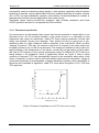
3.1.4 Overcurrent protection
An overcurrent is an abnormally high current that has the potential to cause failure in an
electrical circuit. An out-of-range condition in the power source or a decrease in load
impedance can cause an overcurrent. Used PTC fuses ensures protection of both card
relays and external circuitry from damage. They protect circuitry by going from a lowresistance state to a high resistance state in response to an overcurrent, which is called
“tripping” the device. This way, the current in the circuit is reduced to the value which can
be safely carried by any of the circuit elements. The change of resistance is the result of a
rapid increase in the temperature of the device, caused by the generation of heat within
the fuse by I2R heating. A vary narrow temperature range is sufficient for PTC fuse for a
sharp change in its resistance, which is graphically shown on Figure 2. After a faulty
condition is removed, PTC fuse automatically returns to low resistance state within a few
dozen of seconds, so device can be still used without costly service intervention. Usage of
overcurrent protection is recommended in power distribution systems, where probability of
shortcuts and overloads is significant. Used PTC fuses have recognition of UL, CSA and
TÜV agencies.
Log resistance []
Point 4
Point 1
Point 2
Point 3
Temperature [C]
Figure 2: Example of operating curve for PTC fuse (not to scale)
Page 8 of 32
Copyright, © 2002 Bustec Production Ltd.
ProDAQ 3940 Relay Function Card User Manual
3940-XX-UM
3.1.5 Overvoltage protection
While opening relays, short duration increases in system voltage due to emptying of a
circuit energy storage element such as an inductor may appear. These overvoltage
transients may have significant impact on lifetime of both reed relays and solid state
relays.
When electromechanical relays (including reed relays) are used to control inductive loads,
it is often necessary to derate the contacts to 50% of their resistive load rating due to the
wear caused by the arcing of the contacts. This arcing is caused by the stored energy in
the inductive load. Each time the current in the inductive coil is interrupted by the
mechanical contacts, the voltage across the contacts increases until the contacts arc.
When the contacts arc, the voltage across the arc decreases and the current in the coil
can increase somewhat. The extinguishing of the arc causes an additional voltage
transient which can again cause the contacts to arc. It is not unusual for restriking to occur
several times with the total energy in the arc several times that which was originally stored
in the inductive load. It is this repetitive arcing that is so destructive to the contacts. To
prevent initiation of the arc, optional multilayer surge supressors can be installed on the
board.
When SSRs are used, any voltage that exceeds the SSR’s maximum peak voltage can
potentially damage the relay. Again, this may happen when relays are used to control
inductive loads. In this case, outputs of SSR require an overvoltage suppression device,
like multilayer surge supressors.
3.2
Relays control and synchronous update
For the purpose of relay control, two 16-bit registers RELG1 (group 1, channels 1..8) and
RELG2 (group 2, channels 9..16) are available in the board’s address space. Each bit in
these registers directly controls state of one relay. Write to one of those registers
immediately updates relays state.
For applications where simultaneous switching of relays in different groups is required,
Synchronous Update mode can be used. When the board is configured to work in this
mode, software also writes to registers RELG1 and RELG2, but the state of relays stays
unchanged until required conditions (event) are met. As an event updating all relays at a
time, write to special UPDATE register or input trigger can be selected.
For more detailed description of board registers refer to chapter 3.4.
3.3
Trigger system
3.3.1 Input trigger
Input trigger is used to update both relay groups synchronously. There are possible three
input trigger sources: trigger through the Front Panel connector (FPITRIG), trigger from the
switch matrix on the MB and software trigger (SW2ITRIG). More than one source can be
selected at a time. The input trigger configuration is shown on the Figure 3.
Copyright, © 2002 Bustec Production Ltd.
Page 9 of 32
3940-XX-UM
ProDAQ 3940 Relay Function Card User Manual
FPITRIG
FPITRIG_ALOW
FP2ITRIG_EN
ITRIG_STS
FROM SWITCH MATRIX
ON MB
MB2ITRIG_EN
INPUT TRIGGER
SW2ITRIG
Figure 3: The input trigger configuration
Note that the state of the relays is updated only when input trigger becomes active (card must be
earlier configured to work in Synchronous Update mode). There are two consequences of such
behaviour:
when one of the input trigger sources is already active, no event updating relays is
generated if another input trigger source becomes active
to generate series of events updating relays with software trigger, software has to write
to SW2ITRIG bit zeros and ones alternately.
3.3.2 Output trigger
The output trigger is located on the MB-FC connector and it goes to the MB switch matrix.
Then it can be directed to any trigger line connected to the switch matrix. There is only one
output trigger source – input trigger signal generated internally. The output trigger system
can generate the pulse or the level. If the level has been selected, the output trigger stays
active as long as the source of the trigger is active. If the pulse is selected, pulse of 125 ns
width is generated when output trigger source signal becomes active.
The output trigger configuration scheme is shown on the Figure 4.
OTRIG_STS
INPUT TRIGGER
PULSE GENERATOR
0
1
TRIGGER
TO MB
OTRIG_EN
OTRIG_LEVEL
Figure 4: The output trigger configuration
Output trigger is especially useful when input trigger through the Front Panel connector
(FPITRIG) is used in the system. It can inform the host (for example through interrupt) that
input trigger arrived and an action, like write new values to relay configuration registers
RELG1 and/or RELG2, must be taken.
Page 10 of 32
Copyright, © 2002 Bustec Production Ltd.
ProDAQ 3940 Relay Function Card User Manual
3.4
3940-XX-UM
Register description
3.4.1 Address map and registers
All addresses are given in hexadecimal notation. FC_ADR is address in FC address space.
VXI_ADR is address in VXI address space. The appropriate address offset depends on the
function card position on the motherboard (refer to the motherboard manual).
FC_
ADR
VXI_
ADR
Access
Register Name
0
1
2
3
4
5
6
7
8
9
A
FB
FC
FE
0
4
8
C
10
14
18
1C
20
24
28
3EC
3F0
3F8
FCID
FCVER
FCCSR
FCLEN
reserved
OTRI
ITRI
TEST
UPDATE
RELG1
RELG2
FCEPC
FCSUB
FCSERH
FF
3FC
FCSERL
Function
FPGA internal registers
RO FC ID register
RO FC version register
RW Function card Control and Status Register
RO Size of installed FIFO
Copyright, © 2002 Bustec Production Ltd.
RW
RW
RW
WO
RW
RW
RW
RO
RO
RO
Output trigger control register
Input trigger control register
Test register
Update register
Relay group 1 control register
Relay group 2 control register
EEPROM Control register (for factory usage only)
Function Card sub-type register
Upper 16-bit of the serial number of the function
card
Lower 16-bit of the serial number of the function
card
Page 11 of 32
3940-XX-UM
3.5
ProDAQ 3940 Relay Function Card User Manual
Register Details
3.5.1 FCID
FC_ADR=0H, VXI_ADR=0H
FCID register contains identification number of function card type. Readout should give value of
3940H.
Bit
Operation
Initial
Content
15
RO
0
14
RO
0
13
RO
1
12
RO
1
11
RO
1
10
RO
0
9
RO
0
8
RO
1
7
RO
0
6
RO
1
5
RO
0
4
RO
0
3
RO
0
2
RO
0
1
RO
0
0
RO
0
FC identification number = 3940H
3.5.2 FCVER
FC_ADR=1H, VXI_ADR=4H
This is FC version register. Readout from this register gives information about board revision and
firmware version.
Bit
Operation
Initial
Content
15
RO
x
14
RO
x
13
RO
x
12
RO
x
11
RO
x
10
RO
x
major
9
RO
x
8
RO
x
7
RO
x
6
RO
x
minor
5
RO
x
4
RO
x
3
RO
x
major
FPGA version
2
RO
x
1
RO
x
0
RO
x
minor
PCB version
3.5.3 FCCSR
FC_ADR=2H, VXI_ADR=8H
14
RW
0
Page 12 of 32
13
12
11
10
9
8
7
6
5
4
3
2
1
0
WO
0
Not used
Copyright, © 2002 Bustec Production Ltd.
RESET
15
RW
0
SYNCSRC
Bit
Operation
Initial
Content
SYNCUPDT
Control and Status register allows to switch board into Synchronous Update mode and to select
event which will update all relays.
ProDAQ 3940 Relay Function Card User Manual
RESET
3940-XX-UM
This bit resets all relays to their default state (open) and resets
configuration bits to initial state.
Write
0: Has no effect
1: Resets all relays and configuration bits in FCCSR, ITRI and OTRI
registers to their initial state.
Read
Always gives ‘0’.
This bit selects the source of a synchronous update signal.
Write
0: write to UPDATE register updates state of all relays
1: input trigger updates state of all relays
Read
Gives the last written value
USAGE
Synchronous Update must be selected with SYNCUPDT bit
If input trigger signal is used to update relays, one of the input
trigger sources must be enabled in ITRI register
This bit switches board to Synchronous Update mode, in which all
relays can be updated synchronously.
SYNCSRC
SYNCUPDT
Write
0: Synchronous Update mode is OFF
1: Synchronous Update mode is ON
Read
Gives the last written value
3.5.4 FCLEN
FC_ADR=3H, VXI_ADR=CH
This is register containing information about size of installed FIFO. Readout should always give
0000H because no FIFO is used on this card.
Bit
Operation
Initial
Content
15
RO
0
14
RO
0
13
RO
0
12
RO
0
11
RO
0
10
RO
0
9
RO
0
8
RO
0
7
RO
0
6
RO
0
5
RO
0
4
RO
0
3
RO
0
2
RO
0
1
RO
0
Size of installed FIFO = 0000H
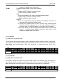
3.5.5 OTRI
FC_ADR=5H, VXI_ADR=14H
Output trigger register allows to control whether the output trigger will be sent to the MB and
whether output trigger will be generated as a level or pulse. There is only one output trigger source
– input trigger signal generated internally.
The output trigger can be used to generate an interrupt to the host computer after input trigger
arrived.
Copyright, © 2002 Bustec Production Ltd.
Page 13 of 32
0
RO
0
OTRIG_ STS
Operation
Initial
Content
15
RO
0
OTRIG_EN
OTRIG_LEVEL
OTRIG_STS
Page 14 of 32
14
13
12
11
10
9
8
Not used
7
6
5
4
3
2
1
RW
0
0
RW
0
OTRIG_EN
Bit
ProDAQ 3940 Relay Function Card User Manual
OTRIG_LEVEL
3940-XX-UM
This bit is the output trigger enable bit. If this bit is cleared no output
trigger will be sent to MB. If this bit is set output trigger to MB will be
generated if trigger source becomes active.
Write
0: output trigger disabled
1: output trigger enabled
Read
Gives the last written value
USAGE
Output trigger enabling bit
This bit is for selection of the output trigger generating mode:
Pulse – after a rising edge of a trigger source pulse of 125 ns width
will be generated independently of trigger source high level duration
Level – after a rising edge a trigger source output trigger level will
follow the level of trigger source.
Write
0: output trigger generating mode set to pulse
1: output trigger generating mode set to level
Read
Gives the last written value
USAGE
When working with interrupts to the host the level mode should
be set
The state of the output trigger line.
Write
No effect
Read
0: output trigger inactive
1: output trigger active
USAGE
When working with interrupts to the host this bit should be
used by the interrupt routing to determine the interrupt source
Copyright, © 2002 Bustec Production Ltd.
ProDAQ 3940 Relay Function Card User Manual
3940-XX-UM
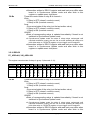
3.5.6 ITRI
FC_ADR=6H, VXI_ADR=18H
The register allows selection of the trigger source which will be used to update state of all relays
simultaneously in Synchronous Update mode and/or will be sent as an output trigger to MB.
These are the three possible input trigger sources:
trigger through the Front Panel connector (FPITRIG)
FPITRIG_
ALOW
FP2ITRIG_EN
11
10
9
8
Not used
7
6
5
4
3
RW
0
2
RW
0
1
RW
0
0
RW
0
FPITRIG_ ALOW
12
FP2ITRIG_EN
13
MB2ITRIG_EN
14
ROC
0
SW2ITRIG
Operation
Initial
Content
15
RO
0
TRIGCOME
Bit
ITRIG_STS
trigger from the switch matrix on the MB
software trigger
To be able to use input trigger to update state of all relays simultaneously, board must be properly
configured:
Synchronous Update mode must be selected (bit SYNCUPDT in FCCSR register set to
‘1’)
Input trigger register must be selected as a source of update signal (bit SYNCSRC in
FCCSR register set to ‘1’)
This bit sets the active level of the external trigger coming from the
Front Panel (ALOW stands for Active LOW).
Write
0: active level high
1: active level low
Read
Gives the last written value
This bit enables the external trigger through the Front Panel connector
(FPITRIG) as a source of input trigger.
Write
0: external trigger disabled
1: external trigger enabled
Read
Gives the last written value
USAGE
The active level of external trigger can be set using
FPITRIG_ALOW bit
Copyright, © 2002 Bustec Production Ltd.
Page 15 of 32
3940-XX-UM
ProDAQ 3940 Relay Function Card User Manual
MB2ITRIG_EN
SW2ITRIG
TRIGCOME
ITRIG_STS
This bit enables the MB trigger as a source of input trigger.
Write
0: MB trigger disabled
1: MB trigger enabled
Read
Gives the last written value
This bit sets the software-generated input trigger.
Write
0: inactive state of the software-generated input trigger
1: active state of the software-generated input trigger
Read
Gives the status of software-generated input trigger
USAGE
To generate series of events updating relays with software trigger,
software has to write to SW2ITRIG bit zeros and ones alternately.
This bit gives information if input triggers arrived since last readout of
ITRI register.
Write
Has no effect
Read
1: Trigger arrived after last readout of ITRI register.
0: No trigger arrived after last readout of ITRI register.
USAGE
To check whether trigger arrived without using interrupts
Readout from ITRI register clears TRIGCOME bit
Current state of the input trigger. The status shows OR function of all
enabled sources of input trigger.
Write
Has no effect
Read
0: input trigger inactive
1: input trigger active
3.5.7 TEST
FC_ADR=7H, VXI_ADR=1CH
Test register is Read/Write register dedicated to be used during production test.
Bit
Operation
Initial
Content
15
RW
0
Page 16 of 32
14
RW
0
13
RW
0
12
RW
0
11
RW
0
10
RW
0
9
RW
0
8
RW
0
7
RW
0
6
RW
0
5
RW
0
4
RW
0
3
RW
0
2
RW
0
1
RW
0
0
RW
0
Read/Write test register
Copyright, © 2002 Bustec Production Ltd.
ProDAQ 3940 Relay Function Card User Manual
3940-XX-UM
3.5.8 UPDATE
FC_ADR=8H, VXI_ADR=20H
15
WO
x
14
WO
x
13
WO
x
12
WO
x
11
WO
x
10
WO
x
9
WO
x
8
WO
x
7
WO
x
6
WO
x
5
WO
x
4
WO
x
3
WO
x
2
WO
x
1
WO
x
0
WO
x
2
RW
0
1
RW
0
0
RW
0
RLA1
Operation
Initial
Content
RLB1
Bit
RLA2
This register is used in Synchronous Update mode. Write to this register (written data doesn’t
matter) updates state of all relays simultaneously. To achieve that, board must be properly
configured:
Synchronous Update mode must be selected (bit SYNCUPDT in FCCSR register set to
‘1’),
write to UPDATE register must be selected as a source of update signal (bit SYNCSRC
in FCCSR register set to ‘0’)
In opposite to synchronous update with software trigger, every write to UPDATE register generates
event updating relays (there is no need to write zeros and ones alternately to generate series of
updates).
UPDATE register
3.5.9 RELG1
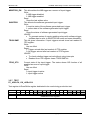
FC_ADR=9H, VXI_ADR=24H
RLAx
13
RW
0
12
RW
0
11
RW
0
10
RW
0
9
RW
0
8
RW
0
7
RW
0
6
RW
0
5
RW
0
4
RW
0
3
RW
0
RLA7
RLB6
RLA6
RLB5
RLA5
RLB4
RLA4
RLB3
RLA3
RLB2
14
RW
0
RLB7
15
RW
0
RLA8
Bit
Operation
Initial
Content
RLB8
This register controls state of relays in group 1 (channels 1..8).
These bits control state of relay A in channel x.
Write
0: Relay is OFF (doesn’t conduct current)
1: Relay is ON (conducts current)
Read
Gives actual state of the relay (not the last written value)
0: Relay is OFF (doesn’t conduct current)
1: Relay is ON (conducts current)
USAGE
State of corresponding relays is updated immediately if board is not
switched to Synchronous Update mode.
In Synchronous Update mode the state of relays stays unchanged until
required conditions (event) are met. As an event updating all relays at a
time either write to UPDATE register or input trigger can be selected.
Copyright, © 2002 Bustec Production Ltd.
Page 17 of 32
3940-XX-UM
ProDAQ 3940 Relay Function Card User Manual
Information written to RELG1 register and read back may differ when
board is in Synchronous Update mode and after write to this
register no update event took place
These bits control state of relay B in channel x.
Write
0: Relay is OFF (doesn’t conduct current)
1: Relay is ON (conducts current)
RLBx
Read
Gives actual state of the relay (not the last written value)
0: Relay is OFF (doesn’t conduct current)
1: Relay is ON (conducts current)
USAGE
State of corresponding relays is updated immediately if board is not
switched to Synchronous Update mode.
In Synchronous Update mode the state of relays stays unchanged until
required conditions (event) are met. As an event updating all relays at a
time either write to UPDATE register or input trigger can be selected.
Information written to RELG1 register and read back may differ when
board is in Synchronous Update mode and after write to this
register no update event took place.
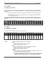
3.5.10 RELG2
FC_ADR=AH, VXI_ADR=28H
RLAx
RLB14
RLA14
RLB13
RLA13
RLB12
6
RW
0
5
RW
0
4
RW
0
3
RW
0
2
RW
0
1
RW
0
0
RW
0
RLA9
7
RW
0
RLB9
8
RW
0
RLA10
9
RW
0
RLB10
10
RW
0
RLA11
11
RW
0
RLB11
12
RW
0
RLA12
13
RW
0
RLA15
14
RW
0
RLB15
15
RW
0
RLA16
Bit
Operation
Initial
Content
RLB16
This register controls state of relays in group 2 (channels 9..16).
These bits control state of relay A in channel x.
Write
0: Relay is OFF (doesn’t conduct current)
1: Relay is ON (conducts current)
Read
Gives actual state of the relay (not the last written value)
0: Relay is OFF (doesn’t conduct current)
1: Relay is ON (conducts current)
USAGE
State of corresponding relays is updated immediately if board is not
switched to Synchronous Update mode.
In Synchronous Update mode the state of relays stays unchanged until
required conditions (event) are met. As an event updating all relays at a
time either write to UPDATE register or input trigger can be selected.
Information written to RELG2 register and read back may differ when
board is in Synchronous Update mode and after write to this
Page 18 of 32
Copyright, © 2002 Bustec Production Ltd.
ProDAQ 3940 Relay Function Card User Manual
3940-XX-UM
register no update event took place.
These bits control state of relay B in channel x.
Write
0: Relay is OFF (doesn’t conduct current)
1: Relay is ON (conducts current)
RLBx
Read
Gives actual state of the relay (not the last written value)
0: Relay is OFF (doesn’t conduct current)
1: Relay is ON (conducts current)
USAGE
State of corresponding relays is updated immediately if board is not
switched to Synchronous Update mode.
In Synchronous Update mode the state of relays stays unchanged until
required conditions (event) are met. As an event updating all relays at a
time either write to UPDATE register or input trigger can be selected.
Information written to RELG2 register and read back may differ when
board is in Synchronous Update mode and after write to this
register no update event took place.
3.5.11 FCSUB
FC_ADR=FCH, VXI_ADR=3F0H
This is function card sub-type register useful for software to distinct between versions of the board.
This register is automatically loaded during board initialisation with contents of on-board EEPROM
chip, which takes approximately 10ms after power-up or deasserting reset signal from
motherboard.
Bit
Operation
Initial
Content
15
RO
x
14
RO
x
13
12
11
10
RO RO RO
RO
x
x
x
x
First letter (ASCII)
9
RO
x
8
RO
x
7
RO
x
6
RO
x
5
4
3
2
RO
RO
RO
RO
x
x
x
x
Second letter (ASCII)
1
RO
x
0
RO
x
Function card sub-type (e.g. “AA”)
3.5.12 FCSERH
FC_ADR=FEH, VXI_ADR=3F8H
This register contains the upper 16-bit of the serial number of the function card. This register is
automatically loaded during board initialisation with contents of on-board EEPROM chip, which
takes approximately 10ms after power-up or deasserting reset signal from motherboard.
Bit
Operation
Initial
Content
15
RO
x
14
RO
x
13
RO
x
12
RO
x
11
RO
x
Copyright, © 2002 Bustec Production Ltd.
10
RO
x
9
RO
x
8
RO
x
7
RO
x
6
RO
x
5
RO
x
4
RO
x
3
RO
x
2
RO
x
1
RO
x
Upper 16-bit of serial number
Page 19 of 32
0
RO
x
3940-XX-UM
ProDAQ 3940 Relay Function Card User Manual
3.5.13 FCSERL
FC_ADR=FFH, VXI_ADR=3FCH
This register contains the lower 16-bit of the serial number of the function card. This register is
automatically loaded during board initialisation with contents of on-board EEPROM chip, which
takes approximately 10ms after power-up or deasserting reset signal from motherboard
Bit
Operation
Initial
Content
15
RO
x
Page 20 of 32
14
RO
x
13
RO
x
12
RO
x
11
RO
x
10
RO
x
9
RO
x
8
RO
x
7
RO
x
6
RO
x
5
RO
x
4
RO
x
3
RO
x
2
RO
x
1
RO
x
Lower 16-bit of serial number
Copyright, © 2002 Bustec Production Ltd.
0
RO
x
ProDAQ 3940 Relay Function Card User Manual
3940-XX-UM
4. Software Utilities
4.1
Introduction
The ProDAQ 3940 VXIplug&play compatible driver package encompasses the instrument
driver, soft front panel, documentation and examples. The VXIplug&play soft front panel is
a graphical user interface application developed for the instrument. It is used to verify the
instrument operation and functionality when the instrument is first integrated into a system.
It provides instrument control in a user-friendly environment, being both Windows 95 and
NT framework compatible. The soft front panel application uses the installed driver to
control and operate the instrument.
4.2
Soft Front Panel
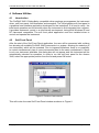
After the start of the Soft Front Panel application, the user will be presented with a dialog
box showing all available ProDAQ 3940 instruments in a system, allowing the selection of
one instrument, which will be operated. Due to imposed limitations, there is no possibility
to control simultaneously two or more instruments fitted to the same motherboard. If there
is only one instrument available, this dialog box will not appear and this instrument will be
automatically selected for operation. In order to run the soft front panel for the chosen
3940, select the appropriate position from the list and press OK button.
Figure 5: Function Card selection
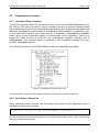
This will invoke the main Soft Front Panel window as shown in Figure 6.
Copyright, © 2002 Bustec Production Ltd.
Page 21 of 32
3940-XX-UM
ProDAQ 3940 Relay Function Card User Manual
Figure 6: Main panel
The main panel of the soft front panel shows the relays grouped in pairs as they are
arranged on the function card. The relays within the pairs can be operated separately or,
when exclusive mode is selected, in dependence of the state of the other relay in the pair.
The soft front panel allows selecting an update mode as asynchronous or synchronous. In
latter case the “Trigger” or “Update” buttons are activated, according to the selected
synchronisation mechanism.
While working in synchronous mode the “Synchronized” LED control signals the relay
update state, a green colour means that the state is up to date, read colour means that the
relays state has changed in registers but it awaits update command or trigger in order to
be switched. When the LED is green the buttons state on the main panel reflects the
relays state.
Page 22 of 32
Copyright, © 2002 Bustec Production Ltd.
ProDAQ 3940 Relay Function Card User Manual
4.3
3940-XX-UM
Programming Concepts
4.3.1 Instrument Driver Overview
To use the instrument driver for the Relay Function Card, one ProDAQ Motherboard, e.g.
the 3120 or 3150, has to be used. In new 2.x version of drivers, a common interface library
was implemented to act as an intermediate layer between the motherboard hardware and
the driver, handling the communication to the different motherboards in a transparent way.
In turn now every function card driver acts as a standalone VXIplug&play compatible
driver, using its own instrument handle to communicate to the instrument. There is no
longer the need to have a driver for the motherboard installed, although this is
recommended. The common library is included to the installation package for every
ProDAQ VXIplug&play driver.
The Instrument driver for the ProDAQ 3940 provides the following functionality:
Figure 7: Instrument Driver function tree
A full description of the instrument driver functions can be found in the driver help file.
4.3.2 Error/Status Information
Every instrument driver function has the same return type format. Returning either a
completion code or an error code.
ViStatus _VI_FUNC bu3940_functionName ( Parameters… );
In order to identify the successful operation of any function these codes can be used. The following
example illustrates this principle.
Copyright, © 2002 Bustec Production Ltd.
Page 23 of 32
3940-XX-UM
ProDAQ 3940 Relay Function Card User Manual
ViSession vi;
ViStatus error;
ViChar msg[512];
:
:
error = bu3940_reset(vi);
if(error < VI_SUCCESS)
{
bu3940_error_message (vi, error, msg);
/* stop execution */
}
else if(error > VI_SUCCESS)
{
bu3940_error_message (vi, error, msg);
/* print a warning and continue execution */
}
If an error occurs, a value less than VI_SUCCESS is returned. The function
bu3940_error_message converts the error code into a readable string. All driver functions
operate along the same principles, so any errors in hardware access are easily
determined.
If a warning occurs, a value greater than VI_SUCCESS is returned. The same function
bu3940_error_message can be used to convert the warning code into readable string.
4.3.3 Connecting to the instrument
A typical initialization sequence is as following:
bu3940_init ("VXI::1::INSTR", VI_TRUE, VI_TRUE, &viSession);
bu3940_fcSelect (viSession, 2); /*use function card in pos.2 */
The call of function bu3940_fcSelect is obligatory and has to be issued after
bu3940_init() function but before calling any other bu3940_ function. Although, for
convenience, another function is provided which encompasses the functionality of those
two function calls:
bu3940_paramInit ("VXI::1::INSTR", 2, VI_TRUE, VI_TRUE, &viSession);
There is a strong requirement that function bu3940_close should be called when the
instrument is no longer used. Each ProDAQ driver obtains a lock to the motherboard
resource, which is released by bu3940_close function afterwards. This also means that
it is not possible to access two function cards, either the same or different located on the
same motherboard, from two separate system processes, since they would use the same
resource descriptor but different instances of common library DLL. Therefore, the
unmatched bu3940_close call can lock the resource as long as common interface library
is loaded.
Page 24 of 32
Copyright, © 2002 Bustec Production Ltd.
ProDAQ 3940 Relay Function Card User Manual
3940-XX-UM
4.3.4 API Layout
API functions are logically divided into groups, which provide different functionality. Apart
from functions which establish session with the instrument and utility functions defined by
VISA standard, there are control and configuration groups which provide actual
functionality. The Output Control class contains functions which operate on relays both in
asynchronous and synchronous mode. The Configure Functions class contains functions
to configure
4.3.5 Programming instrument
Next few paragraphs discuss step by step instrument setup to operate relays in
asynchronous or synchronous mode. All functions are fully described in the driver help file.
After initialization process the instrument is in asynchronous mode and can be operated
using bu3940_switchRelay() or bu3940_switchABPair() functions.
bu3940_switchRelay (viSession, 3, VI_TRUE);
bu3940_switchABPair (viSession, 2, bu3940_A_ON);
The two function calls in the code snippet above simply switch the relay third on. The
second call additionally switches fourth relay off as it operates on pair of relays.
Following sample shows instrument operation in synchronous mode using software
command to release relays state change.
ViBoolean relaysSet[32] = {0, 1, 1, 0, 0, 1, 0, 0, 0, 1, 1, 0};
ViInt32 i;
/*1 2 3 4 5 6 7 8 9 10 11 12*/
bu3940_setSwitchingMode (viSession, bu3940_SWITCH_SYN_CMD,
bu3940_ITRIG_NONE);
for(i=0; i<32; i++)
bu3940_switchRelay (viSession, i+1, VI_FALSE);
for(i=0; i<12; i++)
bu3940_switchRelay (viSession, i+1, relaysSet[i]);
bu3940_updateRelaysState (viSession);
First of all the switching mode is set to be synchronous with software command to release
change, as the input trigger is irrelevant here it is disabled – the third parameter selected
as bu3940_ITRIG_NONE. The first ‘for’ loop switches all relays off and the second loop
sets relays state according to the ‘relaysSet’ array values, the first twelve relays are in use
only.
Finally after setting the relays to desired state software issues update command to make
relays switched, as we are in synchronous mode the switching takes place only after
synchronization event – in this case software command.
When input trigger is used as a synchronization event bu3940_getTriggerStatus() function
can be use to determine the event occurrence. Another way to notice the input trigger
Copyright, © 2002 Bustec Production Ltd.
Page 25 of 32
3940-XX-UM
ProDAQ 3940 Relay Function Card User Manual
arrival is to install an interrupt service routine which would react on output trigger signal.
The bu3940_enableOutputTrigger() function installs user interrupt service routine for that
purpose.
Page 26 of 32
Copyright, © 2002 Bustec Production Ltd.
ProDAQ 3940 Relay Function Card User Manual
3940-XX-UM
5. Technical Specification
ITEM
Number of Relays
-AA
Relay Type
On-path Resistance
Switch Current
Carry Current1
Switch Voltage
Switch Power Rating
Insulation Resistance
Turn-On Time
Turn-Off Time
Expected Relay lifetime2
Current Consumption
-AB
Relay Type
Overcurrent Protection
Overvoltage Protection
-BA
-BB
On-path Resistance
Switch Current
Carry Current1
Switch Voltage
Switch Power Rating
Insulation Resistance
Turn-On Time
Turn-Off Time
Expected Relay lifetime2
Current Consumption
Relay Type
On-path Resistance
Off-path Resistance
Switch Current
Carry Current1
Switch Voltage
Insulation Resistance
Turn-On Time
Turn-Off Time
Expected Relay lifetime
Current Consumption
Relay Type
Overcurrent Protection
Overvoltage Protection
On-path Resistance
Switch Current
Carry Current1
Switch Voltage
Insulation Resistance
Turn-On Time
Turn-Off Time
Expected Relay lifetime
Current Consumption
Copyright, © 2002 Bustec Production Ltd.
SPECIFICATION
32 (16 independent channels)
Ruthenium-plated Reed Relays
< 0.3 (initial)
0.5 A max.
1.0 A max. (per common terminal)
24 V max.
10 W max.
> 1012
< 0.5 msec
< 0.25 msec
109 operations
300 mA (+5V)
Ruthenium-plated Reed Relays
PTC Resettable Fuse
Multilayer Transient Voltage Surge Supressor
Leakage Current 10A
< 0.6 (initial)
0.5 A max.
0.5 A max.
24 V max.
10 W max.
> 1012
< 0.5 msec
< 0.25 msec
109 operations
300 mA (+5V)
Solid State Relays
< 0.7
> 108
0.9 A max.
0.9 A max.
24 V max.
> 1012
< 2.0 msec
< 0.5 msec
Unlimited
500 mA (+5V)
Solid State Relays
PTC Resettable Fuse
Multilayer Transient Voltage Surge Supressor
Leakage Current 10A
< 1.0
0.5 A max.
0.5 A max.
24 V max.
> 1012
< 2.0 msec
< 0.5 msec
Unlimited
500 mA (+5V)
Page 27 of 32
3940-XX-UM
ProDAQ 3940 Relay Function Card User Manual
ITEM
Overcurrent protection characteristics
Type
Hold current
Trip current
Time to trip
Maximum voltage
Reset time
Resistance
Dissipated power3
Overvoltage protection characteristics
Type
Non-repetitive surge current (8/20 s)
Non-repetitive surge energy (10/1000 s)
Leakage current
Response time
Typical capacitance
Trigger Input
Maximum input voltage
Input type
Negative threshold
Positive threshold
Histeresis
Active Polarity
Connectors
Dimensions
PCB construction
Weight
Operating temperature
Storage temperature
SPECIFICATION
Ressetable PTC fuse
0.75 A @ 25C, 0.61 A @ 50C
1.5 A
0.3 s (max.) @ 8.0 A
24V
< 120s
0.29 (max.)
0.6W
Multilayer transient voltage surge supressor
30A (max.)
0.1 J
10 A (max.)
< 5.0 ns
75 pF
5V
Schmitt trigger
1.5 V (typ.)
2.5 V (typ.)
1.0V (typ.)
Software selectable
50-pin SCSI female
230 x 52.6 mm
6-layer PCB
<100g
0 C to 50 C
-40 C to 70 C
NOTES:
1
If both relays in particular channel are open, current in common path must not exceed 1A. Actual maximum current is limited by PTC
fuse to its hold current value if it is installed.
2
The life of the relay depends entirely upon load condition
3
Dissipated power is useful for calculating whether automatic reset condition for PTC fuse is met. The device will automatically reset,
when V 2
PD
4 RL
where: V = operating voltage of the circuit, RL= Load resistance, PD = dissipated power
Page 28 of 32
Copyright, © 2002 Bustec Production Ltd.
ProDAQ 3940 Relay Function Card User Manual
3940-XX-UM
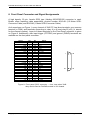
6. Front Panel Connector and Signal Assignments
A high density, 50 pin, female SCSI type (Harting 60010505132) connector is used.
Bustec offers matching cable assemblies, product number 8010-AA (0.5 Meter SCSIConnector Cable) and 8010-AB (1 Meter SCSI-Connector Cable).
As it was shown on Figure 1, every channel of 3940 FC has three terminals: one common
terminal (x-COM), and terminals connecting to relay A (x-A) and relay B (x-B) (‘x’ stands
for the channel number). Layout of those terminals on the Front Panel connector is given
on Figure 8. Additionally, also input trigger (FPITRIG) and ground (DGND) terminals are
available on the front panel connector.
Signal
DGND
16-COM
15-B
15-A
14-COM
13-B
13-A
12-COM
11-B
11-A
10-COM
9-B
9-A
8-COM
7-B
7-A
6-COM
5-B
5-A
4-COM
3-B
3-A
2-COM
1-B
1-A
Pin
1
2
3
4
5
6
7
8
9
10
11
12
13
14
15
16
17
18
19
20
21
22
23
24
25
Pin
26
27
28
29
30
31
32
33
34
35
36
37
38
39
40
41
42
43
44
45
46
47
48
49
50
Signal
FPITRIG
16-B
16-A
15-COM
14-B
14-A
13-COM
12-B
12-A
11-COM
10-B
10-A
9-COM
8-B
8-A
7-COM
6-B
6-A
5-COM
4-B
4-A
3-COM
2-B
2-A
1-COM
1
26
25
50
Figure 8: Front panel SCSI connector – front view when 3940
relay card is fitted on ProDAQ module in VXI chassis.
Copyright, © 2002 Bustec Production Ltd.
Page 29 of 32
3940-XX-UM
ProDAQ 3940 Relay Function Card User Manual
To simplify connection of field wiring to 3940 relay function card, together with a SCSI
cable we recommend using Signal Conditioning Unit 5010-AA with Terminal Block Card
5421-AA. To determine which terminal block connects to a particular channel of 3940
function card, use the following table:
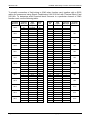
Terminal
Block no.
Terminal
Block pin
3940
signal
SCSI
Pin
TB25
IN
FPITRIG
26
OUT
DGND
1
GND
–
SCSI
Pin
3940
signal
Terminal
Block pin
25
1-A
-
50
1-COM
+
–
GND
Terminal
Block no.
–
TB24
TB23
TB22
TB21
TB20
TB19
TB18
TB17
TB16
TB15
TB14
TB13
Page 30 of 32
+
16-B
27
-
16-COM
2
GND
–
+
16-A
28
-
15-B
3
GND
–
+
15-COM
29
-
15-A
4
GND
–
+
14-B
30
-
14-COM
5
GND
–
+
14-A
31
-
13-B
6
GND
–
+
13-COM
32
7
-
13-A
GND
–
+
12-B
33
8
-
12-COM
GND
–
+
12-A
34
-
11-B
9
GND
–
+
11-COM
35
-
11-A
10
GND
–
+
10-B
36
11
-
10-COM
GND
–
+
10-A
37
-
9-B
12
GND
–
+
9-COM
38
-
9-A
13
24
1-B
-
49
2-A
+
–
GND
23
2-COM
-
48
2-B
+
–
GND
22
3-A
-
47
3-COM
+
–
GND
21
3-B
-
46
4-A
+
–
GND
20
4-COM
-
45
4-B
+
–
GND
19
5-A
-
44
5-COM
+
–
GND
18
5-B
-
43
6-A
+
–
GND
17
6-COM
-
42
6-B
+
–
GND
16
7-A
-
41
7-COM
+
–
GND
15
7-B
-
40
8-A
+
–
GND
14
8-COM
-
39
8-B
+
–
GND
TB1
TB2
TB3
TB4
TB5
TB6
TB7
TB8
TB9
TB10
TB11
TB12
Copyright, © 2002 Bustec Production Ltd.
Bustec Production, Ltd.
World Aviation Park, Shannon, Co. Clare, Ireland
Tel: +353 (0) 61 707100, FAX: +353 (0) 61 707106
Bustec, Inc.
35486 Lorain Road, North Ridgeville, OH 44039, U.S.A
Tel. +1 440 327 8930, Fax: +1 440 327 8982