1
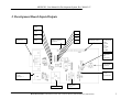
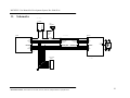
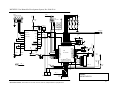
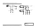
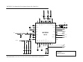
MICRF505: User Manual for Development System, Rev 2004 05 07
MICRF505
User Manual for Development System
915 MHz
Rev. 2004 05 07
Micrel Semiconductor, 1849 Fortune Dr. San Jose, CA 95131,USA Tel: (408) 944-0800 Fax: (408) 944-0970
1
MICRF505: User Manual for Development System, Rev 2004 05 07
Table of contents:
1.
2.
Introduction................................................................................................................. 3
Development Board Inputs/Outputs ........................................................................... 5
2.1.
Summary of DIP-Switch Setting ........................................................................ 6
3. Getting Started ............................................................................................................ 7
4. RF Test Modes............................................................................................................ 8
5. 2-way Link Test Mode.............................................................................................. 11
6. Interface in Byte Transfer Modes ............................................................................. 13
7. Simple Byte Transfer Mode...................................................................................... 15
8. Advanced Byte Transfer Mode................................................................................. 17
9. PC program: RF TestBench ...................................................................................... 19
10.
Firmware change/upgrade..................................................................................... 21
11.
Schematics ............................................................................................................ 22
Micrel Semiconductor, 1849 Fortune Dr. San Jose, CA 95131,USA Tel: (408) 944-0800 Fax: (408) 944-0970
2
MICRF505: User Manual for Development System, Rev 2004 05 07
1. Introduction
This document, “MICRF505 User Manual for Development System” describes the
features of the development system. The development system is made of 2 “development
boards”. For details on the MICRF505 transceiver (a product in the “RadioWireTM”
product line): Please refer to the appropriate data sheet. For the latest updates on products
related to RadioWireTM, please visit www.micrel.com.
Outline of this document:
Following this introduction, an overview of the board’s inputs/outputs is given. Then a
Get-started chapter is included, and the different modes of operation are described. An
overview of how to program/update the firmware is also included. Finally, schematics are
given.
Purpose of the Development system:
The development system provides hands-on experience with the MICRF505 transceiver.
The user can use the included software and hardware, or make a new program and flash it
into the micro controller. That is, the user can use the boards both to evaluate the
MICRF505 chip, and as an aid in the development of a radio communication system.
A separate PC program is available. Through this program, it is possible to set the
programming word for the MICRF505 chip (both the frequency dividers and the control
bits can be set). At present, this program is referred to as “RF TestBench”.
Main modes of operation of the development system:
• RF Test Modes. The user can test the RF properties of the transceiver. It is possible
to transmit a 1010… pattern (default: 38462 transitions/sec), to transmit a carrier or to
stay in receive mode, searching for a 1010… pattern (default: 38462 transitions/sec).
•
2-way Link-Test Mode. In this mode of operation, one board is “Master” and
another board is “Slave”. Messages (the alphabet) are transmitted back and forth
between the two boards. This mode is useful when testing radio communication in
different environments, testing antennas, testing encapsulation etc. Automatic
hopping between 25 frequencies is implemented to meet the FCC part 15.247
regulations. CRC is implemented. A LED (“LED1”) indicates link OK.
•
Simple Byte Transfer Mode. In this mode, the user can enter a number of bytes into
a development board. The board will tell the user to stop/start entering bytes via the
CTS pin. If there is no delay between bytes, 64 bytes can be entered before the board
says “stop”. The board will then transmit the bytes (and say “start” to user). If no
user-bytes are entered, the board will search for RF messages, and, if found, output
the message to the user (if user is ready, indicated by the RTS pin). CRC is
Micrel Semiconductor, 1849 Fortune Dr. San Jose, CA 95131,USA Tel: (408) 944-0800 Fax: (408) 944-0970
3
MICRF505: User Manual for Development System, Rev 2004 05 07
implemented (messages received through RF are only given to user if the CRC is
OK).
•
Advanced Byte Transfer Mode. In this mode of operation, one board is “Master”
and another board is “Slave”. Operates like the “Simple Byte Transfer Mode”, except:
When transmitting user data, the board will construct a frame by adding frame type,
frame ID and sync info. Automatic hopping between 25 frequencies is implemented
to meet the FCC part 15.247 regulations. ARQ, CRC and duplicate control are
implemented as well. “Master” is responsible for maintaining the link (by
transmitting “timestamps”). If “Slave” is reset or gets out of sync, it requests a
“timestamp” from Master.
Development System Features:
•
•
•
•
•
•
•
•
•
•
•
•
•
915 MHz band
25 pre-programmed frequencies: f0 = 903 MHz, f1 = 904 MHz, f2 = 905 MHz, …
f23 = 926 MHz and f24 = 927 MHz1.
Flash-based micro controller (PIC18LF4320) for easy firmware upgrade/testing. Plug
directly into ICD2 from Microchip.
Antenna: External antenna
User interface: RS232 interface or interface through I/O pins.
4 DIP switches to select mode of operation
1 LED to indicate power on
1 LED to indicate RF powered
4 LEDs to indicate status or control information
Possible to use 5 external I/O pins
Possible to observe the interface between RF chip and micro controller via header
pins
Possible to measure RF-part power consumption
In 2-way Link Test Mode and Byte Transfer Modes: Bits to transmit are Manchester
encoded. That is, every bit is coded into 2 elements. The bit rate is 19231 bps, the
element rate is 38462 elements/sec (that is: the actual on-the-air rate is 38462
elements/sec).
Power supply:
• 6 - 9 volt DC
• Apply “ - “ to the centre pin (note!)
External antenna connector:
Type: SMA
1
Automatic hopping in ”2-way Link Test Mode” and “Advanced Byte Transfer Mode” is implemented.
Development boards jump to a new frequency channel approx 10 times/sec. Channels are used randomly.
Micrel Semiconductor, 1849 Fortune Dr. San Jose, CA 95131,USA Tel: (408) 944-0800 Fax: (408) 944-0970
4
MICRF505: User Manual for Development System, Rev 2004 05 07
2. Development Board Inputs/Outputs
DTE_RTS
jumper
DTE_CTS
jumper
LED1
DTE_RX
jumper
LED2
LED3
RS232 connector
9-pin D-sub
DTE_TX
jumper
Header for optional
external i/o
LED4
Header for
MICRF505 interface
1: DATAIXO
2: DATACLK
3:LD
4: RSSI
5: IO
6: SCLK
7:CS
8: GND
MICRF505
RF
Transceiver
SMA antenna
connector
Jumper for RF
power
measuremnet
Power supply/battery
6-9 volt
Center pin: “-“
ICSP connector
DIP-switches
1,2,3,4
Micrel Semiconductor, 1849 Fortune Dr. San Jose, CA 95131,USA Tel: (408) 944-0800 Fax: (408) 944-0970
5
MICRF505: User Manual for Development System, Rev 2004 05 06
2.1. Summary of DIP-Switch Setting
To select mode of operation, bring DIP-switches ON or OFF according to the table
below.
The modes of operation (described in detail in the following sections) are:
• “RF Test Modes”: Enter RX mode, TX a carrier, TX1010… or enter PCconfigurable mode
• “Byte Transfer Mode”: Transfer bytes between e.g. 2 PCs. Select “Simple” or
“Advanced”
• “2-way Link Test Mode”: Use 2 development boards to communicate. If “LED1”
goes on, it indicates “Link OK”.
The 4 DIP-switches (labelled 1 2 3 4) are placed in a single component. In addition “ON”
is written on the component.
DIP1 DIP2 DIP3 DIP4
Mode of operation
--------------------------------------------------------------OFF
OFF
=> Byte transfer modes
OFF
OFF
Simple Byte Transfer Mode
OFF
ON
reserved
ON
OFF
Advanced Byte Transfer Mode, Master
ON
ON
Advanced Byte Transfer Mode,Slave
OFF
ON
ON
ON
OFF
OFF
ON
ON
OFF
ON
OFF
ON
=> Reserved
reserved
reserved
reserved
reserved
OFF
OFF
ON
ON
OFF
ON
OFF
ON
=> 2-Way Link Test Modes
LINK_Test_Master
LINK_Test_Slave
reserved
reserved
OFF
OFF
ON
ON
OFF
ON
OFF
ON
=> RF Test Modes
RF_Test_Rx
RF_Test_Tx1010
RF_Test_TxCarrier
Enable Configuration via PC
OFF
ON
6
Micrel Semiconductor, 1849 Fortune Dr. San Jose, CA 95131,USA Tel: (408) 944-0800 Fax: (408) 944-0970
MICRF505: User Manual for Development System, Rev 2004 05 06
3. Getting Started
Before power-up of the development board:
•
•
•
Get familiar with the inputs/outputs (refer to “Development Board
Inputs/Outputs”)
Select mode of operation via DIP-switches
If Byte Transfer Mode (“Simple” or “Advanced”) is selected: Select interface:
Insert the 4 jumpers “DTE_RTS”, “DTE_CTS”, “DTE_RX”, “DTE_TX” to select
RS232 interface. Remove the jumpers to select “logical level” interface (connect
to e.g. another micro controller). Note: Always power-on the boards with the
RS232 cable disconnected. After power-on: Connect a RS232 cable if wanted.
To get familiar with the boards, the following sequence is suggested:
First, try the 2-way Link Test Mode. On one board, set only DIP1 ON. This will be the
“Master”. On the other board: Set DIP1 and DIP4 ON. This will be the “Slave”. Try to
increase/decrease the distance between the boards, and observe LED1 at the boards. If
LED1 at the Master is on: A 2-way link is established (from Master to Slave and back to
Master). LED1 at the Slave will be on as long as the link from Master to Slave is OK.
Then try the RF Test Mode. (Common to all RF Tests: DIP1 and DIP2 ON). Set one
board to transmit 1010 … (DIP3 OFF, DIP4 ON), and another board to receive (DIP3
and DIP4 OFF). Observe LED1 on the receiving board (indicates received 1010… OK).
Optionally, use an oscilloscope to observe the DATACLK and DATAIXO pins (refer
“Development Board Inputs/Outputs”).
Set the boards in Simple Byte Transfer Mode (all DIPs off). Connect each board in
Simple Byte Transfer Mode to a PC running HyperTerminal. Send characters or text files
between the PCs. Note: No ARQ is used – number of “data packets” getting through
depends on link quality. Make sure the cable is 1:1, and that RTS, CTS, TX, RX and
GND are used. Make sure the data format is 9600-8-N-1 and hardware handshake is used.
Also make sure the jumpers for RS232-use are in place.
Finally, set two boards in Advanced Byte Transfer Mode. Set one as “Master”, the other
as “Slave”: Only DIP3 ON for the “Master”, both DIP3 and DIP4 ON for the “Slave”.
Select RS232 interface (that is, make sure RS232 jumpers are in place) and connect the
boards to PCs. Start HyperTerminal (or other “terminal” program) and observe that text
written on one PC are received and displayed on the other one and v.v. Try e.g. to
transmit a textfile (note: textfile) from one PC to the other. ARQ is used in this mode;
that is: all “data packets” should get through.
7
Micrel Semiconductor, 1849 Fortune Dr. San Jose, CA 95131,USA Tel: (408) 944-0800 Fax: (408) 944-0970
MICRF505: User Manual for Development System, Rev 2004 05 06
4. RF Test Modes
In RF Test Modes, only 1 frequency (915.0MHz) is available. (Or the User can enter
another frequency through the PC program, refer to chapter 9).
DIP-switch setting: (note that both DIP1 and DIP 2 are ON for all RF tests)
Combin. #
1
2
3
4
DIP1
ON
ON
ON
ON
DIP2
ON
ON
ON
ON
DIP3
OFF
OFF
ON
ON
DIP4
OFF
ON
OFF
ON
Text
Receive mode only
Transmit 1010… (38462/sec)
Transmit carrier
Enable configuration via PC
Combination #1, Receive mode only:
The board will continuously search for a 1010… pattern. The board searches for a pattern
with evenly spaced transitions; the searched time between transitions is 26 micro sec
(38462 transitions/sec).
The board utilizes the on-board bit synchronizer feature of the MICRF505.
If a 1010… pattern is received: LED1 will be on. If an error in the 1010… pattern is
detected, LED1 will be off for at least ½ second. The LED1 “off-time” is set to ½ second
to let the user visually observe an error.
The received data is also clocked out directly to a header. DATACLK and DATAIXO are
available at the header close to the antenna-side:
Test points in header; Pin #8 is the one near the “antenna-side”:
8 Gnd
7 CS (Chip Select)
6 SCLK (Programming clock-line)
5 IO (Programming data-line)
4 RSSI (Received signal strength indicator; analogue level)
3 LD (Lock detect)
2 DATACLK (Data clock)
1 DATAIXO (Data input/output)
Combination #2, Transmit 1010… :
The board will enter transmit mode and transmit a 1010… pattern. 38462 transitions/sec
are made. This can be combined with Combination #1 (Receive mode) to test range and
error rate. Combination #2 can be used to test parameters like deviation and transmit
spectrum.
8
Micrel Semiconductor, 1849 Fortune Dr. San Jose, CA 95131,USA Tel: (408) 944-0800 Fax: (408) 944-0970
MICRF505: User Manual for Development System, Rev 2004 05 06
Combination #3, Transmit carrier:
The board will enter transmit mode and transmit a carrier, that is: no modulation is
applied. This can be used to check the frequency spectrum, the output power, and the
current consumption.
Combination #4, Enable configuration via PC:
This setting is also referred to as “PC mode”.
Refer to the chapter called “PC program” for details on the PC program.
Make sure the 4 jumpers “DTE_RTS”, “DTE_CTS”, “DTE_RX” and “DTE_TX” are in
place.
Make sure the board is powered-on without the RS232 cable connected, and then connect
the cable.
Entering “PC mode”: Before any command is given from the PC, the RF chip will stay in
receive or transmit mode, depending on the selected mode before entering “PC mode”.
While in “PC mode”: When a control word is sent from the PC to the board, the board
will store the entered word in EEPROM and program the RF chip with it.
It is possible to transfer a control word from 2 dialog boxes (press the “Transfer” button
inside the dialog box):
Main menu ÆRF TestBench ÆQuick Setup or
Main menu ÆRF TestBench ÆComplete Setup
Note: If giving a “TX1010” command from the PC (selectÆRF TestBench
ÆDevelopment Board Commands): Make sure the board is in transmit mode first.
When leaving “PC mode”: The board will use the default control word already
programmed into the flash program memory, or it will use the control word entered from
the PC program and stored in the EEPROM. Which one to select (the source of the
control word) is selected in the PC program (selectÆRF TestBench ÆDevelopment
Board Commands)2.
From the PC program, try e.g. to change the output power level (PA setting) and observe
the effect on spectrum, power consumption and link range.
2
The “EEPROM control word” can be used in “RF Test Mode”, “2-way Link Test Mode” and “Simple
Byte Transfer Mode”. It will not be used in “Advanced Byte Transfer Mode”. If the “EEPROM control
word” is used in “2-Way Link Test Mode”: No frequency jumping is done – only the control word stored in
EEPROM will be used.
9
Micrel Semiconductor, 1849 Fortune Dr. San Jose, CA 95131,USA Tel: (408) 944-0800 Fax: (408) 944-0970
MICRF505: User Manual for Development System, Rev 2004 05 06
Suggestions for RF Testing:
1) Set one board to transmit a carrier. Use a spectrum analyser to observe the
frequency spectrum. Repeat for transmit 1010…
2) Set one board to receive mode and another to transmit 1010… Use an
oscilloscope to observe the tx’ed and rx’ed data (Data I/O). Set tx’ed data as the
trigger source.
3) Set one board in receive-mode. Turn the other board off and use a signal
generator to input a 1010… pattern. Increase/Decrease the output power level
from the signal generator and observe LED1 and the rx’ed data. This can be used
to test the sensitivity: As long as the LED1 is on, the board is able to read a
1010… pattern. Although a random pattern should be used in sensitivity
measurements, this test gives an indication of the possible detectable signal level.
10
Micrel Semiconductor, 1849 Fortune Dr. San Jose, CA 95131,USA Tel: (408) 944-0800 Fax: (408) 944-0970
MICRF505: User Manual for Development System, Rev 2004 05 06
5. 2-way Link Test Mode
DIP-switch setting:
Combin. #
1
2
DIP1
ON
ON
DIP2
OFF
OFF
DIP3
OFF
OFF
DIP4
OFF
ON
Text
Master
Slave
In this mode of operation, one card is “Master”, and the other is “Slave”.
If not overruled from the PC-program, 25 frequencies are used (refer to “RF Test Mode:
Enable configuration via PC”. Automatic hopping between the 25 frequencies is
implemented to meet the FCC part 15.247 regulations.
Combination #1, Master:
The following procedure is implemented for a “2-Way Link Test Master”:
LOOP
Enter transmit mode on frequency n (n = 0…24)
Transmit “Message” and CRC checksum. Message = characters A…Z (26 bytes)
Enter receive mode on frequency n
Search for ack. Ack = Message = characters A…Z (26 bytes)
If ack found: LED1 on
If no ack for 5 attempts: LED1 off
Use “next frequency” (randomly selected) next time
END_LOOP
The message is transmitted at 19231 bps, Manchester encoded; that is 2*19231 = 38462
signal elements/sec.
CRC (16 bits) is used.
LED1 will go on if an ack is received, and will go off if no ack is received during 5
attempts.
Note: If LED1 at Master is ON, it indicates 2-way communication OK, because:
•
•
•
•
Master has to transmit message correctly,
Slave has to receive message correctly,
Slave has to transmit ack correctly, and finally,
Master has to receive ack correctly – only then is LED1 set ON.
A new message is transmitted every 100 msec (approximately).
11
Micrel Semiconductor, 1849 Fortune Dr. San Jose, CA 95131,USA Tel: (408) 944-0800 Fax: (408) 944-0970
MICRF505: User Manual for Development System, Rev 2004 05 06
Combination #2, Slave:
The following procedure is implemented for a “2-Way Link Test Slave”:
LOOP
Enter receive mode on frequency n (n = 0…24)
Search for Message. Message = characters A…Z (26 bytes)
If Message found:
LED1 on
Enter transmit mode on frequency n
Transmit ack and CRC checksum. Ack = Message = characters A…Z (26
bytes)
If no Message for 5 attempts: LED1 off
Use “next frequency” (randomly selected) next time
END_LOOP
The ack is transmitted at 19231 bps, Manchester encoded; that is 2*19231 = 38462 signal
elements/sec.
CRC (16 bits) is used.
LED1 will go on if a message is received, and will go off if no message is received
during 5 attempts.
Note: If LED1 at Slave is ON, it indicates 1-way communication OK, because:
•
•
Master has to transmit message correctly and
Slave has to receive message correctly – only then is LED1 set ON
After reset or if Slave gets out of Sync, it starts to jump “slowly”: It stays on every
frequency a “long time”: At least long enough for master to transmit a “Message” on all
the frequencies.
Master/Slave sync mechanism in 2-way Link Test:
Both Master and Slave have an internal timer with a period of approx. 100 msec.
The internal timer of the master is never changed. Whenever a period is reached (timer
wrap-around), the Master will enter transmit-mode, transmit a message, turn to receive
mode and search for “ack”. If ack is received or not received: At the next wrap-around, a
“new” frequency is entered and the procedure is repeated.
The internal timer of the Slave is reset whenever a message from the Master is received.
Then the Slave enters transmit-mode and transmits “ack”, then it enters receive mode at
the next frequency and start to search for a new message.
12
Micrel Semiconductor, 1849 Fortune Dr. San Jose, CA 95131,USA Tel: (408) 944-0800 Fax: (408) 944-0970
MICRF505: User Manual for Development System, Rev 2004 05 06
6. Interface in Byte Transfer Modes
In “Simple” or “Advanced” Byte Transfer Mode: Interface to the board in the following
way.
Select interface:
• Insert the 4 jumpers (A, B, C, D) to select RS232 interface.
• Remove the 4 jumpers (A, B, C, D) to select logic levels. Connect jumper
pins directly to e.g. a micro controller).
The board is treated as a DCE (data communications equipment).
The connected user is treated as a DTE (data terminal equipment).
That is, a DCE-DTE cable should be used. This cable should be 1:1, that is: Connect pin i
on the DCE side to pin i on the DTE side. The following pins are used (referred to a 9-pin
connector, names related to DTE):
Pin #
(both DTE and DCE)
2
3
7
8
5
Name (DTE side)
Direction
DTE
DCE
RX
TX
RTS
CTS
Ground
Interface setting:
Baudrate
Number of databits
Parity
Number of stopbits
Handshake:
9600
8
None
1
RTS/CTS
The interface works as follows:
Note that “active state” of RTS and CTS is “low” (a logical “0” seen by the micro
controller).
RTS is an output from DTE (the user). It is used to control data flow from DCE (the
board) to DTE. DTE brings RTS active to signal “DTE ready for data bytes from DCE”.
DTE brings RTS inactive to signal “DTE not ready for data bytes from DCE”. Before
DCE outputs bytes to DTE, the RTS line is tested. If RTS is active, DCE knows that DTE
is ready to receive bytes, and DCE transfer the bytes on the RXD line.
13
Micrel Semiconductor, 1849 Fortune Dr. San Jose, CA 95131,USA Tel: (408) 944-0800 Fax: (408) 944-0970
MICRF505: User Manual for Development System, Rev 2004 05 06
CTS is an input to the DTE. It is used to control data flow from DTE to DCE. DCE
brings CTS active to signal “DCE ready for bytes from DTE”. DCE brings CTS inactive
to signal “DCE not ready for bytes from DTE”. Before DTE outputs bytes to DCE, the
CTS line is tested. If CTS is active, DTE knows that DCE is ready to receive bytes, and
DTE transfer the bytes on the TXD line.
Maximum number of bytes to transmit in one “batch” is 64 bytes. The board will signal
“stop sending bytes” by setting CTS inactive when 64 bytes are read. Note: the board can
buffer 2 additional bytes. Other bytes will be lost.
The bytes can be entered with random delay between them, but if the data line (TX) is
idle for more than 5 msec (no new start bit), the board assumes end-of-transfer from user.
After end-of-transfer is detected, the buffered bytes are transmitted via the MICRF505.
14
Micrel Semiconductor, 1849 Fortune Dr. San Jose, CA 95131,USA Tel: (408) 944-0800 Fax: (408) 944-0970
MICRF505: User Manual for Development System, Rev 2004 05 06
7. Simple Byte Transfer Mode
DIP-switch setting:
Combin. #
1
DIP1
OFF
DIP2
OFF
DIP3
OFF
DIP4
OFF
Text
Note: There is no “Master” or “Slave” in this mode of operation.
Combination #1:
Refer to interface description in “Interface in Byte Transfer Modes”.
There is no difference between “master” and “slave” in this mode.
Error detection (CRC 16 bit) is implemented.
Only 1 frequency is used (no frequency hopping)
Duplicate control or ARQ (packets being acknowledged or re-transmitted) are not
implemented in this mode.
Data flow from UserA to BoardA , then to BoardB and finally to UserB:
1) If Board A is ready to get bytes (CTS is active): UserA enters bytes into BoardA
2) Bytes are buffered in BoardA. When 64 bytes are entered, or >5msec since last
byte; BoardA constructs a frame (it adds preamble, sync, length and CRC).
BoardA then transmits the frame and BoardB receives it.
3) When the frame is completely received by BoardB: The CRC is tested. If CRC is
OK: BoardB gives the data to UserB if UserB is ready (RTS is active)
UserA
BoardA
BoardB
UserB
1)
2)
3)
15
Micrel Semiconductor, 1849 Fortune Dr. San Jose, CA 95131,USA Tel: (408) 944-0800 Fax: (408) 944-0970
MICRF505: User Manual for Development System, Rev 2004 05 06
Example, how to use Simple Byte Transfer Mode:
User A (connected to board A) wants to transfer 6 bytes (= “Hello!”). User B (connected
to board B) receives the bytes.
User A:
•
•
Board A:
•
•
•
•
•
•
Board B:
•
•
•
•
•
Test if CTS at board A is active. If CTS is active, the board is ready to accept
bytes from the user.
Transfer “Hello!” into the board, using 9600-8-N-1. Transfer lsb of every byte
first (after the start-bit).
Read 6 bytes from User A
Detect TX idle for > 5 msec
Format the packet to transmit (the 6 bytes “Hello!”)
Enter transmit mode
Transmit the packet using Manchester encoding
Enter Receive mode
Receive a packet
Un-pack the bytes from the packet
Test that the number of bytes is a legal number of bytes (1-64)
Test that CRC is OK
Test if RTS is active. If RTS is active, the user is ready to accept bytes from
the board.
Transfer the 6 bytes “Hello!” to the User. Transfer lsb of every byte first.
•
User B:
Read 6 bytes from board
Note:
Since no addressing is used, other users (let’s say User C, User D and User E) will
receive the 6 bytes as well. If the boards are used in a network, the message has to
include some address information (and the user’s protocol has to handle it).
16
Micrel Semiconductor, 1849 Fortune Dr. San Jose, CA 95131,USA Tel: (408) 944-0800 Fax: (408) 944-0970
MICRF505: User Manual for Development System, Rev 2004 05 06
8. Advanced Byte Transfer Mode
DIP-switch setting:
Combin. #
1
2
DIP1
OFF
OFF
DIP2
OFF
OFF
DIP3
ON
ON
DIP4
OFF
ON
Text
Master
Slave
Make sure one board is master and one is slave.
This mode of operation has a similar functionality as “Simple Byte Transfer Mode”; in
addition, some “advanced” features are included (described below).
Error detection (CRC 16 bit) is implemented.
Stop-and-wait ARQ (packets being acknowledged or re-transmitted) is implemented.
This means: A “source” (Master or slave) sends a frame to a “destination” (master or
slave). The frame must be ack’ed by the destination, or else the source will retransmit the
frame. If the source is Slave, it will give up transmitting after approximately 25 seconds
(the time-out for no sync-info from master). If the source is Master, it will not quit until
DIP-switches are changed or the board is powered off.
Duplicate control is implemented. If the frame-ID of a “data frame” is equal to the last
received frame-ID, the frame is identified as a duplicate. The frame is ack’ed, but no data
is given to user.
Note: After power-on the boards establish contact (get synchronised). The master board
keeps the boards in synch by transmitting a timestamp every 4 seconds (approximately).
If the slave does not get a timestamp for 25 seconds (approximately), it starts to transmit
timestamp requests.
In Advanced Byte Transfer Mode, LED3 is set on when a message is transmitted, and
LED4 is set on when a message is received. This is done to visualize the RF activity.
Please read the examples below.
Example 1: Every time Master transmits a “timestamp”, a short flash can be seen on
LED3 at the Master-board. And, if the Slave receives the timestamp, a short flash can be
seen on LED4 at the Slave-board.
Example 2: When a Slave is reset, it starts to transmit requests for timing info. This can
be seen as short flashes on LED3. Then, when the slave receives timing info from Master,
a short flash can be seen on LED4, and the flashing of LED3 stops. This can be used to
visually identify “Master and Slave are sync’ed”.
Example 3: When a Master is reset, it will transmit timestamps for approx 3 seconds to
be sure Slave is resync’ed. The LED3 will flash during this period (it appears to be on,
due to short time between transmissions). The Slave will flash LED4 for every timestamp
17
Micrel Semiconductor, 1849 Fortune Dr. San Jose, CA 95131,USA Tel: (408) 944-0800 Fax: (408) 944-0970
MICRF505: User Manual for Development System, Rev 2004 05 06
it receives (it will not receive all, because the jump-pattern is updated when a timestamp
is received).
Automatic hopping between 25 frequencies is implemented to meet the FCC part 15.247
regulations. The units will jump approx. 10 times/second:
There is an internal timer in both Master and Slave. The timer is a 3-byte (24-bit) timer;
the 3 bytes are called Timer_Upper, Timer_High and Timer_Low. A Timer_Low
overflow will generate an interrupt every 0.37msec approx (with a 11.0592MHz xtal
connected to the micro controller). In the interrupt service routine (ISR) the Timer_High
and Timer_Upper registers are updated.
Timer_High will overflow every 256*0.37msec = 94,8msec. This overflow is used to
indicate “time-to-change-frequency” (a flag is set in ISR, the flag is tested in the main
program).
Whenever Timer_High overflows, Timer_Upper is incremented.
When the main program detects time-to-change-frequency, it uses Timer_Upper as an
index in a frequency look-up table, where the frequencies are randomly stored. That is:
The next index will not give the next frequency, but a random frequency.
The internal timer of the master is never changed. The internal timer of the slave is
updated whenever a frame from master is received.
18
Micrel Semiconductor, 1849 Fortune Dr. San Jose, CA 95131,USA Tel: (408) 944-0800 Fax: (408) 944-0970
MICRF505: User Manual for Development System, Rev 2004 05 06
9. PC program: RF TestBench
The PC program is referred to as “RF TestBench”.
The RF TestBench can be used without the development board. It can be used to
calculate fields in the control word to enter into MICRF505. Examples: Find settings for
a specific bitrate.
“RF TestBench” should be self-explaining.
Installation and running are straightforward:
• Copy the files into a separate directory
• Start the program by double-clicking “PCxx.bat” (xx = sw version number)
If using RF TestBench together with an development board:
Make sure the DIP-switches are set like this:
Combin. #
DIP1
DIP2 DIP3 DIP4
ON
ON
ON
ON
1
Text
Using RF TestBench:
•
Power on the board
•
Connect the development board to a PC via a cable:
o 1:1 RS232 cable
o Make sure RTS, CTS, TX, RX and GND are included in the cable (pins 2,
3, 5, 7, 8)
o Note: Power-on the board before connecting the cable to the board
•
•
•
Start RF TestBench by double-clicking “PCxx.bat” (xx = sw version number)
Read the welcome-message
From the main menu, select serial port (COM1 or COM2) via “Setup” Æ
“Communication port”
•
From the main menu, select “RF TestBench” Æ “Quick Setup” or Æ“Complete
Setup”:
o Select “Quick Setup” if you want the program to calculate parameters
based on basic parameters like xtal frequency, RF frequency and bit rate.
Enter values and press the “Calc!” button. To see the resulting control
word fields, press the “See Details” button.
o Select “Complete Setup” to enter the control word fields manually. Press
the “Calc” button to see resulting frequencies etc. Press “More Info”
button to get more information.
19
Micrel Semiconductor, 1849 Fortune Dr. San Jose, CA 95131,USA Tel: (408) 944-0800 Fax: (408) 944-0970
MICRF505: User Manual for Development System, Rev 2004 05 06
o Note that the complete resulting control word can be found in “RF
TestBench” Æ “Overview”
•
To transfer a control word to the development board from “Quick Setup” or
“Complete Setup”: Enter/change the fields and press “Transfer!”. The entered
values are stored in the micro’s EEPROM.
•
Observe the “Status” field. If not “Success!” is displayed, please check
connections/power and try again.
In the following, some suggestions are made for the user to get familiar with “RF
TestBench”.
•
Experiment with e.g. power levels.
•
Try to give a “Transmit 1010” command (ÆRF TestBench ÆDevelopment Board
Commands). Make sure the dev board is in transmit mode first.
•
It is possible to use the pre-programmed settings (stored in the flash program
memory) or the settings stored in EEPROM for the other modes of operation as
well (that is: not only in “PC-mode”). Select “Flash” or “EEPROM” via a
command in RF TestBench (ÆRF TestBench ÆDevelopment Board Commands).
Exception: In Advanced Byte Transfer Mode, only the pre-programmed settings
can be used. Also note: If EEPROM settings are used in 2-way Link Test Mode,
no frequency hopping will be done – only the frequency and control bits stored in
EEPROM will be used.
•
If “EEPROM settings” is selected, the board can be disconnected from the PC,
and the different modes of operation can be run- and now the settings stored in
EEPROM are used. To use the pre-programmed settings again: Enter “PC-Mode”
(DIP-setting described above) and give command from RF TestBench.
•
•
Other possibilities are (ÆRF TestBench ÆDevelopment Board Commands):
Read out the firmware version number (the firmware stored in flash program
memory of the micro controller)
Restart micro controller (uC) program (like a power-on reset)
Reset EEPROM control word - settings to “default” (= pre-programmed settings)
Read out the present EEPROM controlword
•
•
•
20
Micrel Semiconductor, 1849 Fortune Dr. San Jose, CA 95131,USA Tel: (408) 944-0800 Fax: (408) 944-0970
MICRF505: User Manual for Development System, Rev 2004 05 06
10. Firmware change/upgrade
The development boards are equipped with a socket for ICSP (in-circuit serial
programming).
Through ICSP, it is possible to download new firmware into the micro controller.
The download feature is made for use with MPLAB ICD2 from Microchip. Connect the
development board directly to the ICD2 using the cable from the ICD2 kit.
Via ICD2, it’s possible to step through and debug firmware code as well. That is: Make
your own program, download it, debug it and run it!
MPLAB IDE (integrated development environment) is available for free from
Microchip’s homepage. (PC-compiler must be bought).
How to upgrade firmware (“xxx.hex”, xxx=firmware name) (skip reading this if you are
familiar with ICD2):
• Connect ICD2 to your PC and to power (please refer to ICD2 user manual)
• Connect ICD2 and development board via the “standard ICD2 cable”
• Start MPLAB IDE
• Select Configure Æ Select Device… Æ “PIC18F4320” Æ OK
• File ÆImport… Æ “xxx.hex” Æ Open
• Programmer Æ Select Programmer Æ MPLAB ICD2
• Programmer Æ Settings Æ Power Tab : Make sure ”Power target circuit from
MPLAB ICD2” is checked
• Programmer Æ Settings Æ Program Tab : Make sure all fields are checked in the
“Select Memories” box. Æ OK
• Identify and press the “Reset and connect to ICD” button in the main menu field.
• If the “Target not found” warning pops up, repeat steps above.
• Identify and press the “Program target device” button in the main menu field
• Wait for programming to finish (refer to the “Output” window) and remove the
development board from ICD2.
• Optional: Confirm firmware version via RF TestBench
21
Micrel Semiconductor, 1849 Fortune Dr. San Jose, CA 95131,USA Tel: (408) 944-0800 Fax: (408) 944-0970
MICRF505: User Manual for Development System, Rev 2004 05 06
11. Schematics
300 Serie
POWER
2
1
RFVDD
DIGVDD
J101
HEADER 1
POWER
R100
0R
IO
IO
SCLK
CS
RFVDD
IO_MCU
SCLK_MCU
CS_MCU
DATAIXO
DATACLK
DATAIXO_MCU
DATACLK_MCU
LD
RSSI
IO
IO_505
SCLK_505
CS_505
DATAIXO_505
DATACLK_505
IO
SCLK
CS
DATAIXO
DATACLK
2
DIGVDD
LOGIC
RFUNIT
100 serie
5
LOGIC
J100
50ohm line
1
ANT
4 SMA3
LD
RSSI
200 Serie
RFUNIT
EXT_DATA
JP102
10 Serie
1
2
3
4
5
6
7
8
22
Micrel Semiconductor, 1849 Fortune Dr. San Jose, CA 95131,USA Tel: (408) 944-0800 Fax: (408) 944-0970
MICRF505: User Manual for Development System, Rev 2004 05 06
VDD_1
3
5
6
IN1
C1+
IN2
C204
C205
100n
100n
12
2
4
V-
INVALID
V+
FORCEOFF
C2+
C2-
1
1
12
2
12
11
1
20
14
FORCEON
1
EN
SP3223
R212
10R
VDD_1
C207
nc
DATACLK
LD
IO
RC7
RD4
RD5
RD6
RD7
VSS
VDD
AVDD
RB0
RB1
RB2
U200
PIC18LF4320
OSC2
OSC1
VSS
AVSS
VDD
VDD
RE2
RE1
RE0
RA5
RA4
RB3
NC
RB4
RB5
RB6
RB7
!MCLR
RA0
RA1
RA2
RA3
C206
100nF
1
2
3
4
5
6
7
8
9
10
11
12
13
14
15
16
17
18
19
20
21
22
DIGVDD
D203
1
D202
12
2
2
1
2
13
C1-
18
100n
C203
RS232 OUT2
Y201 3
nc
2
C209
nc
VDD_1
Y200
10MHz
R213
10R
C211
22p
JP205
C212
nc
10
9
8
7
6
5
4
3
2
1
C213
100nF
R211
100k
HEADER 10
R210
100k
2
1
RSSI
CS
2
1
33
32
31
30
29
28
27
26
25
24
23
C210
22p
VDD_1
7
SCLK
C208
nc
VDD_1
4
10
OUT2
RS232 OUT1
2
100n
C202
DTE_RX
JP201
1
2
DATAIXO
15
OUT1
RS232 IN2
44
43
42
41
40
39
38
37
36
35
34
8
R205 100k
RC6
RC5
RC4
RD3
RD2
RD1
RD0
RC3
RC2
RC1
RC0
17
RS232 IN1
R206 R207 R208 R209
470
470
470
470
R204 100k
1
2
9
GND
16
VCC
19
6u8
U201
DTE_TX
JP200
D201
1
R203 100k
C201
LED2 LED3 LED4
R202 100k
12
1
2
3
4
2
D200
S1
SW DIP-4
R201
10R
5
9
4
8
3
7
2
6
1
LED1
8
7
6
5
1VDD_1
P200
CONNECTOR DB9
JP204
RJ12
PGM
PGC
PGA
GND
VDD
VPP
6
5
4
3
2
1
VDD_1
JP202 JP203
DTE_RTS DTE_CTS
LOGIC
MICRF505DEV1
23
Micrel Semiconductor, 1849 Fortune Dr. San Jose, CA 95131,USA Tel: (408) 944-0800 Fax: (408) 944-0970
MICRF505: User Manual for Development System, Rev 2004 05 06
J300
Q300
BCP56-10
D300
2
1
L300
1
2
BLM11P300
3
1
1
2
3
R300
1k
BAS19
DC-JACK
U300
1
C301
1n
C302
1u5
2
VOUT
5
RFVDD
R303
470R
GND
ON/OFF
CAP
4
2
3
VIN
C303
100nF
1
MIC5255-2.5BM5
2
R301
1k
2
D302
LED301
C305
nc
C308
6u8
R302
1
1k
U301
D301
BZX84C6V2
C300
1u
2
5
R305
470R
GND
ON/OFF
DIGVDD
1
VOUT
CAP
1
2
3
VIN
MIC5255-3.0BM5
4
C304
100nF
12
3
1
D303
LED302
C306
nc
C307
2
6u8
POWER
MICRF505DEV1
24
Micrel Semiconductor, 1849 Fortune Dr. San Jose, CA 95131,USA Tel: (408) 944-0800 Fax: (408) 944-0970
V2P5_2
V2P5_2
V2P5_2
MICRF505: User Manual for Development System, Rev 2004 05 06
R1
6k2
C3
nc
C1
100nF
10nF
25
XTALOUT
3
DIGGND
C9
1.5pF
DIGVDD
26
27
28
GND
30
29
VARIN
CP_OUT
RFGND
VCOGND
31
VCOVDD
32
NC
1
24
4
Y1
2
18k
C8
2
PTATBIAS
XTALIN
23
1
R3
V2P5_1
C2
V2P5_2
R2
0R
TSX 10A, 16MHz
1.5pF
V2P5_3
3
4
L1
CS
RFGND
SCLK
C5
50ohm line
ANT
RFVDD
50ohm line
C6
5
MICRF505
ANT
C4
8n7
8p2
6
2p2
3p3
7
IO
MLF32
RFGND
DATAlXO
GND
DATACLK
22
21
20
19
18
CS
SCLK
IO
DATAIXO
DATACLK
R4
V2P5_3
C10
C11
C12
C13
1n
10nF
1n
1n
NC
17
16
15
14
LD
RSSI
QCHOUT
NC
13
ICHOUT
12
IFVDD
IFGND
11
9
V2P5_2
R5
82k
V2P5_1
V2P5_0
R7
10R
NC
V2P5_0 10
nc
RFVDD
CIBIAS
8
LD
TP1
TP2
RSSI
C7
R6
nc
nc
RFUNIT
MICRF505DEV1
25
Micrel Semiconductor, 1849 Fortune Dr. San Jose, CA 95131,USA Tel: (408) 944-0800 Fax: (408) 944-0970
MICRF505: User Manual for Development System, Rev 2004 05 06
R101
IO_MCU
IO_505
R102
4k7
1k
R103
SCLK_MCU
SCLK_505
R104
4k7
1k
CS_MCU
CS_505
R105
1k
R106
4k7
R107
100k
DATAIXO_MCU
DATAIXO_505
R108
560k
DATACLK_MCU
R109
0R
DATACLK_505
R110
nc
IO
MICRF505DEV1
26
Micrel Semiconductor, 1849 Fortune Dr. San Jose, CA 95131,USA Tel: (408) 944-0800 Fax: (408) 944-0970