1
:HEVLWHKWWSEL]/*VHUYLFHFRP
(PDLOKWWSZZZ/*(VHUYLFHFRPWHFKVXSKWPO
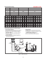
&2/25021,725
6(59,&(0$18$/
&+$66,612&$
02'(/ 6WXGLR:RUNV1% 1%/$/(
6WXGLR:RUNV16 1%/$/0$/%
6WXGLR:RUNV1(1%/$/$)
StudioWorks 73N 73N/$/M
StudioWorks
73E 73N/$/E
6DPHPRGHOIRU6HUYLFH
&$87,21
%()25(6(59,&,1*7+(81,7
5($'7+( 6$)(7<35(&$87,216,17+,60$18$/
0(18
6(/(&7
6DPHORRNLQJZLWKQHZFKDVVLV
,VVXH'DWH:
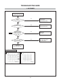
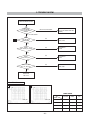
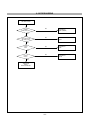
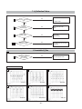
&217(176
30%#)&)#!4)/.3 3!&%4902%#!54)/.3 3%26)#).'02%#!54)/.3
4)-).'#(!24 $)3!33%-",9 !$*534-%.4 7)2).'$)!'2!- ",/#+$)!'2!- $%3#2)04)/./&",/#+$)!'2! 42/5",%3(//4).''5)$% 19
%80,/$%$6)%7 7
2%0,!#%-%.40!243,)34 8
3#(%-!4)#$)!'2!- 4
02).4#)2#5)4"/!2$46
63(&,),&$7,216
3,&785(78%(
3IZE
$EF)ECTION!NGLE
.ECK$IAMETER
$OT0ITCH
&ACE4REATMENT
,OW2ADIATION
0OWER#ONSUMPTION
INCH
MM
MM
7!2!3#!NTI2EFLECTIONAND
!NTI3TATIC#OATING
-02))4#/
6,*1$/
(ORIZONTAL6ERTICAL3YNC
)NPUT6OLTAGE,EVEL ,OW^6(IGH^6
3YNC0OLARITY
0OSITIVEOR.EGATIVE
6IDEO)NPUT3IGNAL
6OLTAGE,EVEL
A#OLOR
B#OLOR
C#OLOR
)NPUT)MPEDANCE
6IDEO#OLOR
3IGNAL&ORMAT
^6PP
6PP
6PP
6PP
7
2'"!NALOG
2EFERTOTHE4IMING#HART
3IGNAL#ONNECTOR
ROWPIN#ONNECTOR!TTACHED
3CANNING&REQUENCY
(ORIZONTAL
6ERTICAL
^K(Z
^(Z
32:(56833/<
0OWER2ANGE
!#6^(Z!-AX
-/$%
0/7%2#/.35-04)/.
,%$#/,/2
-!8
7
'2%%.
./2-!,/.
7
'2%%.
34!.$"9
LESSTHAN7
3530%.$
LESSTHAN7
/&&
LESSTHAN7
)/$6+
)/$6+
',63/$<$5($
!CTIVE6IDEO!REA s-AX)MAGE3IZEXMMX
s0RESET)MAGE3IZEXMM X
$ISPLAY#OLOR
&ULL#OLORS
$ISPLAY2ESOLUTION X(Z-AX
.ON)NTERLACE
6IDEO"ANDWIDTH
-(Z
(19,5210(17
/PERATING4EMPERATURE #^ #
!MBIENT
2ELATIVE(UMIDITY
^
.ONCONDENSING
!LTITUDE
M
',0(16,216ZLWK7,/76:,9(/
7IDTH
MMINCH
$EPTH
11MM17INCH
(EIGHT
7.5MM6INCH
:(,*+7ZLWK7,/76:,9(/
.ET7EIGHT
0KG0.92LBS
'ROSS7EIGHT
KGLBS
SAFETY PRECAUTIONS
SAFETY-RELATED COMPONENT WARNING!
There are special components used in this color monitor
which are important for safety. These parts are marked
on the schematic diagram and the replacement
parts list. It is essential that these critical parts should be
replaced with the manufacturer's specified parts to prevent
X-radiation, shock, fire, or other hazards. Do not modify
the original design without obtaining written permission
from manufacturer or you will void the original parts and
labor guarantee.
CAUTION:
No modification of any circuit should be
attempted.
Service work should be performed only after
you are thoroughly familiar with all of the
following safety checks and servicing
guidelines.
SAFETY CHECK
Care should be taken while servicing this color monitor
because of the high voltage used in the deflection circuits.
These voltages are exposed in such areas as the
associated flyback and yoke circuits.
FIRE & SHOCK HAZARD
An isolation transformer must be inserted between the
color monitor and AC power line before servicing the
chassis.
• In servicing, attention must be paid to the original lead
dress specially in the high voltage circuit. If a short
circuit is found, replace all parts which have been
overheated as a result of the short circuit.
• All the protective devices must be reinstalled per the
original design.
• Soldering must be inspected for the cold solder joints,
frayed leads, damaged insulation, solder splashes, or
the sharp points. Be sure to remove all foreign
materials.
X-RADIATION
The only potential source of X-radiation is the picture tube.
However, when the high voltage circuitry is operating
properly there is no possibility of an X-radiation problem.
The basic precaution which must be exercised is keep the
high voltage at the factory recommended level; the normal
high voltage is about 25.8kV. The following steps describe
how to measure the high voltage and how to prevent Xradiation.
Note : It is important to use an accurate high voltage
meter calibrated periodically.
• To measure the high voltage, use a high impedance
high voltage meter, connect (–) to chassis and (+) to
the CDT anode cap.
• Set the brightness control to maximum point at full
white pattern.
• Measure the high voltage. The high voltage meter
should be indicated at the factory recommended level.
• If the meter indication exceeds the maximum level,
immediate service is required to prevent the possibility
of premature component failure.
• To prevent X-radiation possibility, it is essential to use
the specified picture tube.
CAUTION:
Please use only a plastic screwdriver to protect yourself
from shock hazard during service operation.
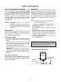
Leakage Current Hot Check Circuit
IMPLOSION PROTECTION
All used display tubes are equipped with an integral
implosion protection system, but care should be taken to
avoid damage and scratching during installation. Use only
same type display tubes.
AC Volt-meter
Good Earth Ground
such as WATER PIPE,
CONDUIT etc.
To Instrument's
exposed
METALLIC PARTS
1.5 Kohm/10W
-3-
SERVICING PRECAUTIONS
CAUTION: Before servicing receivers covered by this
service manual and its supplements and addenda, read
and follow the SAFETY PRECAUTIONS on page 3 of this
publication.
NOTE: If unforeseen circumstances create conflict
between the following servicing precautions and any of the
safety precautions on page 3 of this publication, always
follow the safety precautions. Remember: Safety First.
General Servicing Precautions
1. Always unplug the receiver AC power cord from the AC
power source before;
a. Removing or reinstalling any component, circuit
board module or any other receiver assembly.
b. Disconnecting or reconnecting any receiver electrical
plug or other electrical connection.
c. Connecting a test substitute in parallel with an
electrolytic capacitor in the receiver.
CAUTION: A wrong part substitution or incorrect
polarity installation of electrolytic capacitors may
result in an explosion hazard.
d. Discharging the picture tube anode.
2. Test high voltage only by measuring it with an
appropriate high voltage meter or other voltage
measuring device (DVM, FETVOM, etc) equipped with
a suitable high voltage probe.
Do not test high voltage by "drawing an arc".
3. Discharge the picture tube anode only by (a) first
connecting one end of an insulated clip lead to the
degaussing or kine aquadag grounding system shield
at the point where the picture tube socket ground lead
is connected, and then (b) touch the other end of the
insulated clip lead to the picture tube anode button,
using an insulating handle to avoid personal contact
with high voltage.
4. Do not spray chemicals on or near this receiver or any
of its assemblies.
5. Unless specified otherwise in this service manual,
clean electrical contacts only by applying the following
mixture to the contacts with a pipe cleaner, cottontipped stick or comparable non-abrasive applicator;
10% (by volume) Acetone and 90% (by volume)
isopropyl alcohol (90%-99% strength)
CAUTION: This is a flammable mixture.
Unless specified otherwise in this service manual,
lubrication of contacts in not required.
6. Do not defeat any plug/socket B+ voltage interlocks
with which receivers covered by this service manual
might be equipped.
7. Do not apply AC power to this instrument and/or any of
its electrical assemblies unless all solid-state device
heat sinks are correctly installed.
8. Always connect the test receiver ground lead to the
receiver chassis ground before connecting the test
receiver positive lead.
Always remove the test receiver ground lead last.
9. Use with this receiver only the test fixtures specified in
this service manual.
CAUTION: Do not connect the test fixture ground strap
to any heat sink in this receiver.
Electrostatically Sensitive (ES) Devices
Some semiconductor (solid-state) devices can be
damaged easily by static electricity. Such components
commonly are called Electrostatically Sensitive (ES)
Devices. Examples of typical ES devices are integrated
circuits and some field-effect transistors and
semiconductor "chip" components. The following
techniques should be used to help reduce the incidence of
component damage caused by static by static electricity.
1. Immediately before handling any semiconductor
component or semiconductor-equipped assembly, drain
off any electrostatic charge on your body by touching a
known earth ground. Alternatively, obtain and wear a
commercially available discharging wrist strap device,
which should be removed to prevent potential shock
reasons prior to applying power to the unit under test.
2. After removing an electrical assembly equipped with
ES devices, place the assembly on a conductive
surface such as aluminum foil, to prevent electrostatic
charge buildup or exposure of the assembly.
3. Use only a grounded-tip soldering iron to solder or
unsolder ES devices.
4. Use only an anti-static type solder removal device.
Some solder removal devices not classified as "antistatic" can generate electrical charges sufficient to
damage ES devices.
5. Do not use freon-propelled chemicals. These can
generate electrical charges sufficient to damage ES
devices.
6. Do not remove a replacement ES device from its
protective package until immediately before you are
ready to install it. (Most replacement ES devices are
packaged with leads electrically shorted together by
conductive foam, aluminum foil or comparable
conductive material).
7. Immediately before removing the protective material
from the leads of a replacement ES device, touch the
protective material to the chassis or circuit assembly
into which the device will be installed.
CAUTION: Be sure no power is applied to the chassis
or circuit, and observe all other safety precautions.
8. Minimize bodily motions when handling unpackaged
replacement ES devices. (Otherwise harmless motion
such as the brushing together of your clothes fabric or
the lifting of your foot from a carpeted floor can
generate static electricity sufficient to damage an ES
device.)
-4-
General Soldering Guidelines
1. Use a grounded-tip, low-wattage soldering iron and
appropriate tip size and shape that will maintain tip
temperature within the range or 500 F to 600 F.
2. Use an appropriate gauge of RMA resin-core solder
composed of 60 parts tin/40 parts lead.
3. Keep the soldering iron tip clean and well tinned.
4. Thoroughly clean the surfaces to be soldered. Use a
mall wire-bristle (0.5 inch, or 1.25cm) brush with a
metal handle.
Do not use freon-propelled spray-on cleaners.
5. Use the following unsoldering technique
a. Allow the soldering iron tip to reach normal
temperature.
(500 F to 600 F)
b. Heat the component lead until the solder melts.
c. Quickly draw the melted solder with an anti-static,
suction-type solder removal device or with solder
braid.
CAUTION: Work quickly to avoid overheating the
circuitboard printed foil.
6. Use the following soldering technique.
a. Allow the soldering iron tip to reach a normal
temperature (500 F to 600 F)
b. First, hold the soldering iron tip and solder the strand
against the component lead until the solder melts.
c. Quickly move the soldering iron tip to the junction of
the component lead and the printed circuit foil, and
hold it there only until the solder flows onto and
around both the component lead and the foil.
CAUTION: Work quickly to avoid overheating the
circuit board printed foil.
d. Closely inspect the solder area and remove any
excess or splashed solder with a small wire-bristle
brush.
IC Remove/Replacement
Some chassis circuit boards have slotted holes (oblong)
through which the IC leads are inserted and then bent flat
against the circuit foil. When holes are the slotted type,
the following technique should be used to remove and
replace the IC. When working with boards using the
familiar round hole, use the standard technique as
outlined in paragraphs 5 and 6 above.
Removal
1. Desolder and straighten each IC lead in one operation
by gently prying up on the lead with the soldering iron
tip as the solder melts.
2. Draw away the melted solder with an anti-static
suction-type solder removal device (or with solder
braid) before removing the IC.
Replacement
1. Carefully insert the replacement IC in the circuit board.
2. Carefully bend each IC lead against the circuit foil pad
and solder it.
3. Clean the soldered areas with a small wire-bristle
brush. (It is not necessary to reapply acrylic coating to
the areas).
"Small-Signal" Discrete Transistor
Removal/Replacement
1. Remove the defective transistor by clipping its leads as
close as possible to the component body.
2. Bend into a "U" shape the end of each of three leads
remaining on the circuit board.
3. Bend into a "U" shape the replacement transistor leads.
4. Connect the replacement transistor leads to the
corresponding leads extending from the circuit board
and crimp the "U" with long nose pliers to insure metal
to metal contact then solder each connection.
Power Output, Transistor Device
Removal/Replacement
1. Heat and remove all solder from around the transistor
leads.
2. Remove the heat sink mounting screw (if so equipped).
3. Carefully remove the transistor from the heat sink of the
circuit board.
4. Insert new transistor in the circuit board.
5. Solder each transistor lead, and clip off excess lead.
6. Replace heat sink.
Diode Removal/Replacement
1. Remove defective diode by clipping its leads as close
as possible to diode body.
2. Bend the two remaining leads perpendicular y to the
circuit board.
3. Observing diode polarity, wrap each lead of the new
diode around the corresponding lead on the circuit
board.
4. Securely crimp each connection and solder it.
5. Inspect (on the circuit board copper side) the solder
joints of the two "original" leads. If they are not shiny,
reheat them and if necessary, apply additional solder.
Fuse and Conventional Resistor
Removal/Replacement
1. Clip each fuse or resistor lead at top of the circuit board
hollow stake.
2. Securely crimp the leads of replacement component
around notch at stake top.
3. Solder the connections.
CAUTION: Maintain original spacing between the
replaced component and adjacent components and the
circuit board to prevent excessive component
temperatures.
-5-
Circuit Board Foil Repair
Excessive heat applied to the copper foil of any printed
circuit board will weaken the adhesive that bonds the foil
to the circuit board causing the foil to separate from or
"lift-off" the board. The following guidelines and
procedures should be followed whenever this condition is
encountered.
At IC Connections
To repair a defective copper pattern at IC connections use
the following procedure to install a jumper wire on the
copper pattern side of the circuit board. (Use this
technique only on IC connections).
1. Carefully remove the damaged copper pattern with a
sharp knife. (Remove only as much copper as
absolutely necessary).
2. carefully scratch away the solder resist and acrylic
coating (if used) from the end of the remaining copper
pattern.
3. Bend a small "U" in one end of a small gauge jumper
wire and carefully crimp it around the IC pin. Solder the
IC connection.
4. Route the jumper wire along the path of the out-away
copper pattern and let it overlap the previously scraped
end of the good copper pattern. Solder the overlapped
area and clip off any excess jumper wire.
At Other Connections
Use the following technique to repair the defective copper
pattern at connections other than IC Pins. This technique
involves the installation of a jumper wire on the
component side of the circuit board.
1. Remove the defective copper pattern with a sharp
knife.
Remove at least 1/4 inch of copper, to ensure that a
hazardous condition will not exist if the jumper wire
opens.
2. Trace along the copper pattern from both sides of the
pattern break and locate the nearest component that is
directly connected to the affected copper pattern.
3. Connect insulated 20-gauge jumper wire from the lead
of the nearest component on one side of the pattern
break to the lead of the nearest component on the
other side.
Carefully crimp and solder the connections.
CAUTION: Be sure the insulated jumper wire is
dressed so the it does not touch components or sharp
edges.
-6-
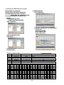
TIMING CHART
VIDEO
C
B
SYNC
D
E
F
A
<< Dot Clock (MHz), Horizontal Frequency (kHz), Vertical Frequency (Hz), Horizontal etc... (µs), Vertical etc... (ms) >>
Mode
1
2
3
4
H/V
Sort
Sync
Polarity
H
–
Total Period
(A)
Video Active
Time (B)
37.50
26.67
20.32
6.35
2.03
3.81
0.51
Frequency
Blanking Time Sync Duration
(E)
(C)
Back Porch
(F)
Front Porch
(D)
V
–
74.99
13.335
12.802
0.533
0.080
0.427
0.026
H
+
46.88
21.33
16.16
5.17
1.62
3.23
0.32
V
+
75.01
13.331
12.798
0.533
0.064
0.448
0.021
H
+
53.68
18.63
14.22
4.41
1.14
2.70
0.57
V
+
85.07
11.755
11.178
0.577
0.056
0.503
0.018
H
+
68.677
14.561
10.836
3.725
1.016
2.201
0.508
V
+
85.00
11.764
11.182
0.582
0.044
0.524
0.014
* No Support Composite Mode.
-7-
Resolution
640x480
75Hz
800x600
75Hz
800x600
85Hz
1024x768
85Hz
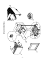
DISASSEMBLY
1. Carefully place the monitor on a soft cushion
and stand it upright with the cabinet facing
downward.
2. Remove the two screws from the back cover.
4. Separate the back cover from the latch at the
bottom of the cabinet using the jig as shown in
the figure.
(Insert the jig into the latch and lift slightly.)
3. Separate the back cover from the latch on top
of the cabinet using a screwdriver as shown in
the figure.
(Insert the screwdriver and gently press the
latch.)
5. Lift up the back cover to separate from cabinet
assembly.
-8-
ADJUSTMENT
1. Preparation for Service Adjustment
2. Adjustment by Service Hot key
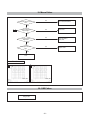
GENERAL INFORMATION
How to enter SVC HOT KEY
All adjustment are thoroughly checked and corrected
when the monitor leaves the factory, but sometimes
several adjustments may be required.
Adjustment should be following procedure and after
warming up for a minimum of 30 minutes.
• Alignment appliances and tools.
- IBM compatible PC.
- Programmable Signal Generator.
(eg. VG-819 made by Astrodesign Co.)
- EPROM or EEPROM with saved each mode data.
- Alignment Adaptor and Software.
- Digital Voltmeter.
- White Balance Meter.
- Luminance Meter.
- High-voltage Meter.
1. Press Menu and OSD window will appear.
2. While OSD window is displayed,
is seen on the
left bottom of OSD window.
3. Press
+ power switch simultaneously and the
screen will immediately refresh.
4. Press Menu and make sure that
is changed to
1 2.
5. Follow the menu on the left of OSD window to find 12
and OSD will change as shown in the figure.
6. Select Degauss in the above figure and then press
Select and
to enter the screen of the SUB menu.
(Back Raster for Pattern)
FOS SPEC
AUTOMATIC AND MANUAL DEGAUSSING
The degaussing coil is mounted around the CDT so that
automatic degaussing when turn on the monitor. But a
monitor is moved or faced in a different direction, become
poor color purity cause of CDT magnetized, then press
DEGAUSSING on the OSD menu.
1. Size
H : 310 4mm
V : 230 4mm
Scanning frequency : All Mode (Mode 1~4)
Display image : Cross hatch pattern
2. Centering
Scanning frequency : All Mode (Mode 1~4)
Display image : Crosshatch pattern
Horizontal : 10 Row
Vertical : 8 Row
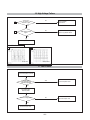
ADJUSTMENT PROCEDURE & METHOD
-
-
U
Install the cable for adjustment such as Figure 1and run
the alignment program on the DOS for IBM
compatible PC.
Set external Brightness and Contrast volume to max
position.
1. Adjustment for B+ Voltage.
D
H:
1) Display cross hatch pattern at Mode 4.
2) Check D961 cathode voltage within 50V ± 1V .
2. Adjustment for High-Voltage.
1) Display cross hatch pattern at Mode 4.
2) Enter the SVC SUB menu as the following instruction.
3) Adjust H/Voltage to 25.8kV±0.1 kV by adjust 1-P value.
R
L
L-R
4mm, V :
U-D
4mm
3. Tilt
Scanning frequency : All Mode (Mode 1~4)
Display image : Crosshatch pattern
Horizontal : 10 Row
Vertical : 8 Row
E
Tilt :
-9-
E-F
2.0mm
F
4. Distortion
Scanning frequency : All Mode (Mode 1~4)
Display image : Crosshatch pattern
Horizontal : 10 Row
Vertical : 8 Row
A
B
E
4mm
G
F
11. Adjustment of white balance (Adjustment of
chromaticity diagram)
*(Adjustment of white balance must be made after
entering Hot Key Mode and DEGAUSS.)
H
C
A-B
E-F
10. Parallelogram
D
2.0mm,
2.0mm,
C-D
G-H
2.0mm
2.0mm
5. Displa Size drift
4mm : 25 Standard, 10
0.5mm : 180V ~ 264V
CONDITIONS
Signal:
69 kHz / 85 Hz
Display image:
Back raster (Color 0,0)
Contrast:
Maximum
Brightness:
Maximum
Color temperature: 9300K
35
11-1. Adjustment of cut off (Adjustment of back raster)
6. Linearity
Y1
11-1(a). Before adjustment, press Menu and Degauss
to remove.
=> Enter hot key mode.
Adjust Brightness and Contrast to Max in OSD
window.
Y2
Y3
Y4
X1 X2 X3 X4
(1) Adjust cut off (back raster) first. Enter DEGAUSS in
the Menu and modify the following data.
Modify RCUT to Min ,
Modify GCUT To Min ,
Adjust to BCUT Data = 127 (7F (h)) ,
Adjust to SBRT Data = 205 ( CD (h)).
(2) Turn FBT screen volume on "CRT COLOR
ANALYZER CA-100" equipment to adjust
Brightness to 0.4
0.05FL.
(3) Adjust RCUT, GCUT, and SBRT to set chromaticity
diagram at :
x: 0.283 0.005
y: 0.298 0.005
Y: 0.40 0.05FL
Formula : (Max - Min) / Max x 100(%)
Criteria : H - 10% Max. (Upper 40kHz)
14% Max. (Less 40kHz)
V - 8% Max.
7. Regulation
2mm
Luminance
Dynamic(lode)
2mm
Scanning frequency : All Mode (Mode 1~4)
8. Trapezoid
U-D < 4mm
U
U
D
D
* If color values would not be matched desirable values,
repeat sequence 1 and 2 after readjusting “GREEN
CUTOFF” control a little different.
9. Pin Balance
L1
L1
R1
R1
2.0mm
L1
R1
- 10 -
$GMXVWPHQWRI:KLWH%DODQFH
$IWHU ILQLVKLQJ DGMXVWPHQW RI FXW RII EDFN UDVWHU
DSSURYH&RORU)XOOZKLWHSDWWHUQ
$GMXVW%'59'DWD 6&21 $GMXVW5'59DQG*'59WRVHWFKURPDWLFLW\GLDJUDPDW
[ \ $SSURYH:LQGRZSDWWHUQ[PPWRDGMXVW
6&21WR< )/
$SSURYH &RORU )XOO ZKLWH SDWWHUQ DJDLQ DQG
DGMXVW$%/'DWDWR< )/
352&('85(
)RUWUDLQHGDQGH[SHULHQFHGVHUYLFHWHFKQLFLDQVRQO\
8VH WKH IROORZLQJ SURFHGXUH WR FRUUHFW PLQRU FRORU
SXULW\SUREOHPV
)RFXV$GMXVWPHQW
0DNH VXUH WKH VSDFLQJ EHWZHHQ WKH 3&0 DVVHPEO\
DQGWKH&57VWHPLVPP PP
&21',7,216
6FDQQLQJIUHTXHQF\
'LVSOD\LPDJH
%ULJKWQHVV
&RQWUDVW
$OO0RGH0RGHa
h+vFKDUDFWHUSDWWHUQ
&XWRIISRLQW
0D[LPXP
0DNH VXUH WKH GLVSOD\ LV QRW DIIHFWHG E\ H[WHUQDO
PDJQHWLFILHOGV
9HU\FDUHIXOO\EUHDNWKHJOXHVHDOEHWZHHQWKHSROH
SXULW\ FRQYHUJHQFH PDJQHWV 3&0 WKH EDQG DQG
WKHVSDFHU
'LVSOD\DJUHHQSDWWHUQRYHUWKHHQWLUHGLVSOD\DUHD
352&('85(
$GMXVW WKH )RFXV 95 RQ WKH )%7 WR GLVSOD\ WKH
VKDUSHVWLPDJHSRVVLEOH
8VH/RFNWLWHWRVHDOWKH)RFXV95LQSRVLWLRQ
$GMXVWWKHSXULW\PDJQHWULQJVRQWKH3&0DVVHPEO\
WRGLVSOD\DSXUHJUHHQSDWWHUQ
2SWLPXPVHWWLQJ[ \ 5HSHDW VWHSV DQG XVLQJ D UHG SDWWHUQ DQG WKHQ
DJDLQXVLQJDEOXHSDWWHUQ
&RORU3XULW\$GMXVWPHQW
&RORUSXULW\LVWKHDEVHQFHRIXQGHVLUHGFRORU
&RQVSLFXRXVPLVODQGLQJXQH[SHFWHGFRORULQDXQLIRUP
ILHOG ZLWKLQ WKH GLVSOD\ DUHD VKDOO QRW EH YLVLEOH DW D
GLVWDQFHRIFPIURPWKH&57VXUIDFH
&21',7,216
2ULHQWDWLRQ0RQLWRUIDFLQJHDVW
6FDQQLQJ)UHTXHQF\ [#+]N+]+]
'LVSOD\LPDJH
:KLWHIODWILHOG
/XPLQDQFH
&XWRIISRLQWDWWKHFHQWHURIWKH
GLVSOD\DUHD
1RWH&RORUSXULW\DGMXVWPHQWVVKRXOGRQO\EH
DWWHPSWHGE\TXDOLILHGSHUVRQQHO
7DEOH&RORU3XULW\7ROHUDQFHV
5HG
[ \ *UHHQ
[ \ %OXH
[ \ )RU.FRORUDGMXVWPHQW[ \ :KHQ \RX KDYH WKH 3&0V SURSHUO\ DGMXVWHG
FDUHIXOO\ JOXH WKHP WRJHWKHU WR SUHYHQW WKHLU
PRYHPHQWGXULQJVKLSSLQJ
3. Adjustment Using Service software Program
(Adjustment Program)
2. Adjustment for White Balance and Luminance.
1. Adjustment for Factory Mode (Preset Mode).
1) Display cross hatch pattern at Mode All.
2) Run alignment program for 710BL/773NL
on the IBM compatible PC.
3) EEPROM → ALL CLEAR → Y(Yes) command.
<Caution> Do not run this procedure unless the
EEPROM is changed. All data in EEPROM (mode
data and color data) will be erased.
4) COMMAND → PRESET START → Y(Yes)
command.
5) DIST. ADJ. → FOS. ADJ command.
6) Adjust H-POSITION as arrow keys to center of the
screen.
7) Adjust H-SIZE as arrow keys to 310 ± 2mm.
8) Adjust V-POSITION as arrow keys to center of the
screen.
9) Adjust V-SIZE as arrow keys to 230 ± 2mm.
10) Adjust TRAPEZOID as arrow keys to be the best
condition.
11) Adjust SIDE PINCUSHON as arrow keys to be the
best condition.
12) Adjust TILT as arrow keys to be the best condition.
13) Display cross hatch pattern at Mode 4.
14) DIST. ADJ. → BALANCE DATA command.
15) Adjust balance of Pin-Balance as arrow keys to be
the best condition.
16) Adjust parallelogram as arrow keys to be the best
condition.
17) Save of the Mode.
18) Save of the System.
19) Display from Mode 4 and repeat above from number
6) to 16).
20) COMMAND → PRESET EXIT → Y (Yes) command.
- 12 -
1) Set the White Balance Meter.
2) Press the DEGAUSSING on the OSD menu for
demagnetization of the CDT.
3) Display color 0,0 pattern at Mode 4.
4) COMMAND → PRESET START → Y(Yes)
command.
5) Set Bightness and Contrast to max position.
6) COLOR ADJ. → LUMINANCE command of the
alignment program.
7) COLOR ADJ. → BIAS ADJ. command of the
alignment program.
8) Check whether blue color or not at R-BIAS and GBIAS to min position, Sub-Brightness to 205
(CD(h))position, B-Bias to 127(7F(h))position. If it's not
blue color, the monitor must repair.
9) Adjust Screen control on the FBT to 0.4 ± 0.05FL
of the raster luminance.
10) Adjust R-BIAS and G-BIAS command to x=0.283 ±
0.006 and y=0.298 ± 0.006 on the White Balance
Meter with PC arrow keys.
11) Display color 15,0 Full White(70x70mm) at mode 4.
12) DRIVE ADJ command.
13) Set B-DRIVE to 90(5A(h)) at DRIVE of the alignment
program.
14) Adjust R-DRIVE and G-DRIVE command to white
balance x=0.283 ± 0.003 and y=0.298 ± 0.003 on
the White Balance Meter with PC arrow keys.
15) Adjust SUB-CONTRAST command to 50±1FL of the
raster luminance.
15) Display color 15,0 full white patten at Mode 4.
16) COLOR ADJ. → LUMINANCE → ABL command.
17) Adjust ABL to 32 ± 1FL of the luminance.
18) Exit from the program.
$GMXVWPHQWDQG(',''DWD'RZQLQ*&6&
(','5HDG:ULWH
5XQ:LQ(','H[H
:LQGRZV(','98VHU0DQXDO
2SHUDWLQJ6\VWHP06:LQGRZV;3
3RUW6HWXS:LQGRZV !'RQWQHHGVHWXS
:LQGRZV;3 !1HHGWR3RUW6HWXS
7KLVSURJUDPLVDYDLODEOHWR/&'0RQLWRURQO\
3RUW6HWXS
D&RS\h8VHU3RUWV\VvILOHWR
hF?:,117?V\VWHP?GULYHUVvIROGHU
E5XQ8VHUSRUWH[H
(GLW:HHNRI0DQXIDFWXUH<HDURI0DQXIDFWXUH
6HULDO1XPEHU
D,QSXW8VHU,QIR'DWD
E&OLFNh8SGDWHvEXWWRQ
F&OLFNh:ULWHvEXWWRQ
F5HPRYHDOOGHIDXOWQXPEHU
G$GG))
H&OLFN6WDUWEXWWRQ
I&OLFN([LWEXWWRQ
(',''$7$(',7%/
1R
,WHP
&RQWHQW
0DQXIDFWXUHU,'
*60
3URGXFW,'
<HDU
9HUVLRQ
5HYLVLRQ
0RGHOQDPH
%
㫸 'DWD
('
$
(
6SHFLDO
$
%
&
'
(
)
))
))
))
))
))
))
(
'
$
(
%
($
$
$
&
))
)(
)
$
($
(
(
)'
$
(
%
$
)&
$
)&
$
(',''$7$(',71/
1R
乍Ⳃ ᷛ⼎ 䖯ࠊ᭄ 0DQXIDFWXUHU,'
*60
('
3URGXFW,'
()
<HDU
(
9HUVLRQ
5HYLVLRQ
0RGHOQDPH
1
(
$
%
&
'
(
)
))
))
))
))
))
))
(
'
()
(
%
(
(
$
%
&
))
)(
)
)
)
)
($
(
(
)'
$
(
%
$
)&
(
$
)&
$
(',' 'DWD (GLW 8VLQJ6HUYLFH VRIWZDUH 3URJUDP
:ULWH (',' 'DWD
'LVSOD\FRORUFURVVKDWFKSDWWHUQDW0RGH 8VH((3520:ULWH(','FRPPDQGDQGFRQILUP
³(',':ULWH2.´PHVVDJHRIPRQLWRU
([LWIURPWKHDOLJQPHQWSURJUDP
3RZHUVZLWFK2))21IRU(','GDWDVDYH
5HDG DQG 0RGLI\ (',' 'DWD
&RQQHFWRUWKHPRQLWRUDQGDGMXVWGHYLFHDV)LJXUH
'LVSOD\FRORUFURVVKDWFKSDWWHUQDW0RGH 8VH(',7±02'(/6(/FRPPDQGWRVHOHFWWKH
ULJKWPRGHOLQIRILOH
8VH(',7±(',',1)2FRPPDQGDQGUHWXUQWR
UHDGWKH(',''DWD
0RGLI\WKH(',''DWDLIQHHGHGDQGXVLQJ)WR
VDYHWKHFKDQJHDQGH[LW
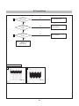
$
,%0
&RPSDWLEOH3&
9,'(2
6,*1$/
*(1(5$725
&
3$5$//(/3257
/
//
(
2))
21
)
3RZHULQOHWUHTXLUHG
9
32
:(
5
9*
$
02
1,7
&6
7
6
25
%
96
<1
&
9
3$
5$
&RQWURO/LQH
56
&
1R
WX
VH
G
3RZHU6HOHFW6ZLWFK
99
3RZHU/('
21
(
.
2))
/6
( 676ZLWFK
%
) 96\QF2Q2II6ZLWFK
6ZLWFKPXVWEH21
)LJXUH&DEOH&RQQHFWLRQ
.
.
9
/6
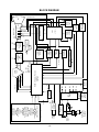
WIRING DIAGRAM
P501(option)
P701
FBT
S+ S
P702
P402
AC
Socket
T1
P902
Signal
Cable
P302
P301
G2
- 15 -
3R Z HU ,Q S X W
a9$ &
+]
/LQ H
)L O W HU
'HJ DX V V L Q J
&L U F X L W
7,/ 7
&R Q W U R O
&L U F X L W
9
60 36
&R Q W U R O
,&
9R O W DJ H
I HHG E DF N
60 36
7
9
(3520
,&
9
'30
&R Q W U R O
&L U F X L W 9
9
9
9
,&
% 'U L Y H
9
9
9
9
%
9
9
&872))&L U F X L W
,&
9,'(2
0DL Q $ 03
,&
5*% % L DV
+/ L Q HDU L W \
&R U U HF W L R Q
+2X W
4
92X W
,&
7'$ -
'&'&&R Q Y HU W HU
+ 'U L Y H
9
;5$ <
3U R W HF W L R Q
&L U F X L W 9,'(2
3U H$ 03
26'
,&
9
'\Q DP L F
)2&86
&L U F X L W
7
)% 7
+9
$X WR
% HDP
/LP L W
'<
5HJ X O DW L R Q
&L U F X L W
''
)HHG % DF N
9
% U L J K W Q HV V &R Q W U R O
* *
+HDW HU 9
&'7
9
'\QDPLF)RFXV
6WDWLF)RFXV
'HJ DX V V L Q J
&R L O
7,/ 7
&R L O
9
9
5
*
%
+6\ Q F 96\ Q F
3:0&R Q W U R O 6L J Q DO 6&/ 6'$
9L G HR
6L J Q D O
0,&20 +96\ Q F 3U R F HV V R U
,&
6$ $ ,&&/ 2&. 6&/ ,&'$ 7$ 6'$ 96\ Q F
+6\ Q F
9
6FUHHQ
> 26'&R Q W U R O @
% 5, *+71(66
&2175$ 67
02,5(
' ( * $ 86 6 , 1 *
+9326,7,21
+96,=(
63&&
75$ 3(=2,'
3,1% $ / $ 1&(
3$ 5$ / / (/ 2*5$ 0
527$ 7,217L O W 5(&$ / / 5(6(7
&2/ 25
,1)250$ 7,21
/ $ 1*8$ *(
26'7,0(
723% 27720&251(5
9,'(2/ (9(/
26'&21752/ / 2&.
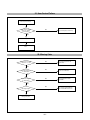
BLOCK DIAGRAM
'(6&5,37,212)%/2&.',$*5$0
3-033WITCHING-ODE0OWER3UPPLY
7HENYOUTURNONTHEPOWERSWITCHTHEOPERATING
PROCEDUREISASFOLLOWS
4HE!#LINEVOLTAGEISRECTIFIEDBYTHEBRIDGEDIODE
$
4HECONTROL)#)#STARTSSWITCHINGANDGENERATES
SWITCHPULSEINTHEPRIMARYTURNOFTHE3-03
TRANSFORMER4
4HESWITCHINGPULSESOFTHEPRIMARYTURNSAREINDUCED
TOTHESECONDARYTURNSOFTHETRANSFORMERBYTHETURN
RATIO4HISPULSESARERECTIFIEDBYEACHDIODE$
$$$$$
%ACHRECTIFIED$#VOLTAGE6666
AND6
$$#ONVERTER#IRCUIT
4OOBTAINCONSTANTHIGHVOLTAGETHISCIRCUITSUPPLIES
CONTROLLED$#VOLTAGEFOR&"4ANDHORIZONTALDEFLECTION
CIRCUITACCORDINGTOTHEHORIZONTALSYNCFREQUENCY
82!90ROTECTION#IRCUIT
7HENTHEHIGH6OLTAGEREACHESTOK6INANABNORMAL
CASETHEHIGHVOLTAGEDETECTORCIRCUIT2$#
2#STARTOPERATIONTOSHUTDOWNHIGHVOLTAGE
CIRCUIT
(ORIZONTAL3CORRECTION#IRCUIT
4HISCIRCUITCORRECTSTHEHORIZONTALLINEARITYFOREACH
HORIZONTALSYNCFREQUENCY
/VER6OLTAGE0ROTECTION#IRCUIT
7HENTHEINPUTOF)#6IN PINISMORETHAN
6ALLTHESECONDARYVOLTAGESOFTHE3-03
TRANSFORMER4DOWNTOLOWVALUE
(ORIZONTALDRIVEAND/UTPUT#IRCUIT
4HISCIRCUITISAHORIZONTALDEFLECTIONAMPLIFIERFORRASTER
SCAN
!",#IRCUIT
4HISCIRCUITLIMITSTHEBEAMCURRENTFORTHERELIABILITYOF
#$4
$ISPLAY0OWER-ANAGEMENT#IRCUIT$0-
34!.$"93530%.$-ODE
7HENNOINPUTOFHORIZONTALORVERTICALSYNC1
1ARETURNEDOFFAND11ARETURNEDOFF
4HENINPUTPOWERCONSUMPTIONISBELOWWATTS
/&&-ODE
7HENNOINPUTOFHORIZONTALANDVERTICALSYNC1
1ARETURNEDOFFAND11ARETURNEDOFF
4HENINPUTPOWERCONSUMPTIONISBELOWWATTS
6ERTICAL/UTPUT#IRCUIT
4HISCIRCUITTAKESTHEVERTICALRAMPWAVEFROMTHE
4$!*)#ANDPERFORMTHEVERTICALDEFLECTION
BYSUPPLYINGTHESAWTOOTHWAVECURRENTTOTHEVERTICAL
DEFLECTIONYOKE
-ICROPROCESSOR#ONTROL(ORIZONTALAND
6ERTICAL3YNC0ROCESSOR#IRCUIT
4HEOPERATINGPROCEDUREISASFOLLOWS
4HEREIS(ORIZONTAL6ERTICALPROCESSFUNCTIONIN
-ICROPROCESSOR)#
-ICROPROCESSOR)#DISCRIMINATESTHEOPERATING
MODEFROMTHESYNCPOLARITYANDRESOLUTION
!FTERMICROPROCESSORREADSTHESEADJUSTEDMODEDATA
STOREDAT%%02/-ITCONTROLSOPERATINGMODEDATA
THROUGH))#
5SERSCANCONTROLSCREENCONDITIONBYTHE/3$3ELECT
5P$OWN,EFT2IGHT%XIT
4HEHORIZONTALANDVERTICALSYNCPROCESSOR)#)#
HASASYNCDETECTORASAWTOOTHGENERATORANDDRIVE
FUNCTION!NDOUTPUTSHORIZONTALANDVERTICALDRIVE
SIGNALTOCONTROLSCREENDISTORTIONS
"LANKINGAND"RIGHTNESS#ONTROL#IRCUIT
"LANKINGCIRCUITELIMINATESTHERETRACELINEBY
SUPPLYINGANEGATIVEPULSEWAVETOTHE'OFTHE#$4
"RIGHTNESSCONTROLCIRCUITISUSEDFORCONTROLOFTHE
SCREENBRIGHTNESSBYCHANGINGTHE$#LEVEL'
)MAGE2OTATION4ILT#IRCUIT
4HISCIRCUITCORRECTSTHETILTOFTHESCREENBY
SUPPLYINGTHEIMAGEROTATIONSIGNALTOTHETILTCOIL
WHICHISATTACHEDNEARTHEDEFLECTIONYOKEOFTHE
#$4
/3$/N3CREEN$ISPLAY#IRCUIT
4HISCIRCUITDISPLAYSINFORMATIONOFTHEMONITOR{SSTATUS
ONTHESCREEN
6IDEO0ROCESSOR#IRCUIT
6IDEO0RE!MP#IRCUIT
6IDEOPROCESSORCIRCUITCONSISTSOFTHEVIDEODRIVE
OUTPUTBLOCK4HEVIDEODRIVE)#)#RECEIVESTHE
VIDEOSIGNALFROM0#4HEGAINOFEACHCHANNELIS
CONTROLLEDBY-)#/-THROUGH))#
4HECUTOFFCIRCUITCOMPENSATEDIFFERENTVOLTAGEOF
EACHCHANNELBETWEENTHECATHODEANDTHE'OFTHE
#$4
4HISCIRCUITAMPLIFIESTHEANALOGVIDEOSIGNALFROM
^6TO^6)TISOPERATEDBYTAKINGTHECLAMP
2'"DRIVEANDCONTRASTSIGNALFROMTHE-)#/-
)#
6IDEO/UTPUT!MP#IRCUIT
4HISCIRCUITAMPLIFIESTHEVIDEOSIGNALWHICHCOMES
FROMTHEVIDEOPREAMPCIRCUITANDAMPLIFIEDITTO
APPLIEDTHE#$4CATHODE
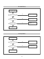
7528%/(6+227,1**8,'(
1232:(5
1232:(5
32:(5,1',&$7252))
&+(&.
)86(2.")
12
7528%/(
,1)86()
60366ZLWFK212))
12
7528%/(,1
%5,'*(',2'('
12
7528%/(,1
,&4
12
7528%/(,1
''''
'''
<(6
&+(&.
'%5,'*(',2'("
<(6
&+(&.
&92/7$*(
9'&DW9LQSXW
9'&DW9LQSXW
,&4
<(6
&+(&.
''''
'''"
<(6
7528%/(,1
4444
:DYHIRUPV
4'UDLQ
,&
12&+$5$&7(5
12&+$5$&7(5
&+(&.
,&3,1
12
7528%/(,1
36,*1$/&$%/(
3&6,*1$/
12
7528%/(,1
,&3
12
7528%/(,1
,&
12
7528%/(,1
,&
<(6
&+(&.
,&3,1
3,19"
<(6
&+(&.
,&3,1
3,19
3,19"
<(6
&+(&.
5*%&$7+2'(
92/7$*("
<(6
7528%/(,1
&'762&.(7
:DYHIRUPV
,&
,&
,&
,&
,&
&'75.*.%.
125$67(5
129,'(2
32:(5,1',&$725
*5((1RU)/$6+
&+(&.
32:(5,1',&$725
*5((1RU)/$6+"
)/$6+
7528%/(,1
36,*1$/&$%/(
*5((1
&+(&.
6&5((1&21752/
.12%2))%7
12
527$7(6&5((1&21752/
.12%72&/2&.:,6(
RU&2817(5&/2&.:,(6
12
7528%/(,135,0$5<
&,5&8,72)7
12
7528%/(,1
&'762&.(7%2$5'
<(6
&+(&.
92/7$*($7
'&$7+2'(9
'&$7+2'(9
'&$7+2'(9
'&$7+2'(
9"
<(6
&+(&.
,&0,&203,1
9+,*+,&3,1
3,13,1
<(6
7528%/(,1
,&0,&20
:DYHIRUPV
,&
,&
,&
129(57,&$/'()/(&7,21
129'()/(&7,21
21(+25,=217$//,1(
&+(&.
,&3LQ9"
12
7528%/(,1
79/LQH
12
7528%/(,1
79OLQH
12
7528%/(,1
,&
<(6
&+(&.
,&3,19"
<(6
&+(&.
,&3,1
6$:7227+:$9("
<(6
7528%/(,1
,&9&,5&8,7
:DYHIRUPV
,&
,&
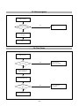
7528%/(,1'30
6WDQGE\6863(1'
'3062))02'()$,/85(
&+(&.
,&0,&20
3,1+9,1387
6,*1$/"
&+(&.3&
3&,6127*2,1*,172'30
02'(
,1387+96<1&6,*1$/
12+96<1&6,*1$/
&+(&.
,&3,1
:$9()250"
12
7528%/(,1
;,&
12
7528%/(,1
,&
12
7528%/(,1
,&
12
7528%/(,1
44
<(6
&+(&.
,&3,19+,*+"
<(6
&+(&.
,&3,1"
<(6
&+(&.% /,1(
9999"
<(6
7528%/(,1
7RU3&
:DYHIRUPV
'3067$%/(
,7(0
+96<1&
9,'(2
/('
1250$5
2121
1250$/
*5((1
67$1'%<
2))21
2))9
)/$6+
6863(1'
212))
2))9
)/$6+
2))
2))2))
2))9
)/$6+
02'(
&
,&
6. NO DEGAUSSING
NO DEGAUSSING
CHECK
IC401 PIN 4 (5V)?
NO
TROUBLE IN
IC401 (MICOM)
NO
TROUBLE IN
D953
NO
TROUBLE IN
P902
NO
TROUBLE IN
RL901
YES
CHECK
Q953 COLLECTOR
VOLTAGE (0.5V)?
YES
CHECK
P902?
YES
CHECK
RL901?
YES
TROUBLE IN
TH901,
DEGAUSSING COIL
- 24 -
+B'HIOHFWLRQ)DLOXUH
,&3LQZDYHIRUPLV
ULJKW"
&KHFN,&3LQV
12
5HSODFH,&
<(6
4GUDLQ
ZDYHIRUPLVULJKW"
12
&KHFN49/,1(
'
12
&KHFN4
&KHFN9OLQH
12
&KHFNDQGUHSODFH7
DQG4&KHFN'<FRQQHFWRU
FRQQHFWLRQ
<(6
4GUDLQ
ZDYHIRUPLVULJKW"
<(6
4EDVHFROOHFWRU
ZDYHIRUPVDUHULJKW"
,QYDULDEOH+B6L]H
&KHFNLI'&YROWDJHRI
,&3,1
ZDYHLV9DULDEOH
12
&KHFNDQGUHSODFH,&
:DYHIRUPV
,&
4'UDLQ
4%DVH
4'UDLQ
4&ROOHFWRU
,&
5. TROUBLE IN H-LINEARITY
UNBALANCED OF H-LIN.
CHECK
IC401
PIN 11, 12, 13 ?
NO
TROUBLE IN
IC401 (MICOM)
NO
TROUBLE IN
Q711 ~ Q716
NO
TROUBLE IN
L703
YES
CHECK
Q711~Q716?
YES
CHECK
L703?
Cs SIGNAL TABLE
YES
HORIZONTAL
FREQUENCY(fH)
30K
34K
39K
44K
49K
52K
58K
62K
66K
TROUBLE IN
C722, C723, C726, C729
- 26 -
~
~
~
~
~
~
~
~
~
33.9K
38.9K
43.9K
48.9K
51.9K
57.9K
61.9K
65.9K
71K
Cs1
Cs2
Cs3
L
L
H
H
H
H
H
H
H
L
H
L
L
H
H
H
H
H
L
L
L
H
L
L
L
H
H
$EQRUPDO+B6L]H
7KH9ROWDJH
ZDYHIRUP4&ROOHFWRU
LVULJKW"
12
5HSHDWWKHWURXEOHVKRRWLQJ
*XLGHRI+BGHIOHFWLRQIDLOXUH
12
&KHFN''FRQYHUWHUFLUFXLW
&KHFN,&%FRQWUROFLUFXLW
<(6
7SLQYROWDJH
LVFKDQJHZLWK+IUHTXHQF\"
6LGH3LQRU7UDS)DLOXUH
&KHFNLI$&
9ROWDJHRI,&3LQ
ZDYHIRUPLV9DULDEOH
12
3DUDRU3LQ%DODQFH)DLOXUH
5HSODFH,&
:DYHIRUPV
4&ROOHFWRU
,&
&KHFNDQGUHSODFH,&
7LOW)DLOXUH
&KHFNWLOWFRQQHFWRU
FRQQHFWLRQ
,&3LQ
RXWSXWGXW\YDULHVZLWK
GLIIHUHQW'$&YDOXHV"
12
&KHFNDQGUHSODFH,&
<(6
4(PLWWHURXWSXWYDULHV
ZLWKGLIIHUHQW'$&YDOXHV"
12
&KHFN444
<(6
&KHFNDQGUHSODFH&57
96L]HRU3RV9DULDWLRQ)DLOXUH
,&3LQ
RXWSXWYDULHVZLWKGLIIHUHQW
'$&YDOXHV"
12
<(6
&KHFNDQGUHSODFH,&
DQG,&
:DYHIRUPV
,&
,&
&KHFNVRPHSDUWVDURXQG,&
+LJK9ROWDJH)DLOXUH
4GUDLQ
ZDYHIRUPLVULJKW"
12
&KHFN44
&KHFN9OLQH
12
5HSHDWWKHWURXEOHVKRRWLQJ
*XLGHRI+BGHIOHFWLRQIDLOXUH
<(6
4FROOHFWHUZDYHIRUP
LVULJKW"
<(6
5HSODFH7
:DYHIRUPV
4'UDLQ4&ROOHFWRU
$%/)DLOXUH
,QSXWIXOOZKLWHSDWWHUQWRPRQLWRU
,&3LQ
LQSXWH[LVWVDQGYDULHV
ZLWKGLIIHUHQWSDWWHUQV"
<(6
&KHFNDQGUHSODFH,&
12
&KHFN3'
5a5
<(6
73LQ9ROWDJHH[LVWV"
12
<(6
&KHFNDQGUHSODFH&57
&KHFNDQGUHSODFH7
)RFXV)DLOXUH
12
,&3LQ
RXWSXWDUHULJKW"
&KHFNDQGUHSODFH,&
<(6
4DQGSDUWVDURXQG
12
5HSODFHIDLOHGSDUW
DUHULJKW"
<(6
6RPHSDUWVDURXQG7
DUHULJKW"
12
<(6
&KHFNWKHFRQQHFWLRQEHWZHHQ
)%73LQ
&576RFNHW3&%
:DYHIRUPV
,&)%7
5HSODFHIDLOHGSDUW
0LFRP)DLOXUH
,&3LQLQSXWLVRYHU
9"
12
&KHFN4'='
<(6
,&3LQDQG
LQSXWVDUHULJKW"
12
&KHFN;
<(6
,&3LQLQSXWLV
+LJK$FWLYH"
12
&KHFNDQGUHSODFH
5&
<(6
$OOLQRXWSXWYDOXHVDUH
ULJKW"
12
<(6
'RQH
:DYHIRUPV
,&
,&
26')DLOXUH
&KDQJH,&
5HSODFH,&
21. User Control Failure
Check connector Ass’y.
IC401 Pins 27 and 28
inputs are right at
each function?
NO
Check and replace function key.
YES
Check and replace IC401.
Done.
22. Missing Color
Proper Video levels are
on P301 Pin 1, 3 and 5.
NO
Check signal generator and
signal cable.
YES
Proper AC voltage are
on all cathodes?
NO
Refer to 2 No Charcter.
YES
Proper DC voltage are
on all cathodes?
NO
Check and replace IC303
and IC304
NO
Check C341, C346 and G2 wire.
Check around FBT circuits also.
YES
G2 voltage is right?
YES
Change the CRT.
- 32 -
23. Visible Retrace
Check white balance adjustment.
G2 voltage is right?
NO
Check G2 control volume and FBT.
YES
Blank pedestal is on
Pin 19, 20 and 21 of IC302
NO
Check IC302
and related components.
NO
Check Q799
and related components.
YES
Is V_FLB and DC_bias on
G1 Pin at CRT socket?
YES
Done.
24. Purity Failure
Degaussing
Purity is right?
YES
Done.
NO
NO
Degaussing circuit is right?
YES
Replace CRT and verify purity.
- 33 -
Refer to 6 NO Degaussing.
25. Misconvergence
Degauss the CDT
Adjust Pole4,Pole6
to improve the misconvergence
Yes
Done
No
Change CRT and readjust
convergence.
Done.
26. Poor Focus
Adjust focus VR.
Improved focus?
YES
Aging monitor and
check for focus change.
NO
Refer to 18 Dynamic
Focus Failure.
NO
Check focus leads from
FBT to CRT Socket.
Check the CRT Socket.
Dynamic focus circuit is
right?
YES
Replace the CRT and verify focus.
- 34 -
- 35 -
2
1
EN
U
M
SE
LE
CT
5
A
6
11-2
B
12
14
c
e
10
15
13
b
d
7
b
11-1
9
8
12
a
14
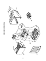
EXPLODED VIEW(710BL)
4
3
%80,/$%$6)%70!243,)34",
5HI1R
3$5712
7.&%
7.&&
7.&'
7.&(
7.&)
7.&*
7.&+
'(6&5,37,21
&$%,1(7$66(0%/<%-%5$1'&6:67635,1*&.'',)RU
$XVWUDOLD035VRXWKHDVW$VLD035(XURSH035,QGRQHVLD03586$&DQDGD0356RXWK
$IULFD035
&$%,1(7$66(0%/<%-%5$1'&76:(',635,1*&.')RUVRXWKHDVW
$VLD(XURSH,VUDHO$VLD8QLWHG.LQGRP9LHWQDP6RXWK$IULFD
&$%,1(7$66(0%/<%-%5$1'&3&$%66:%0$$',5$1)RU(XURSH7&2
&$%,1(7$66(0%/<%.%5$1'&76:(/*5('',)RU&KLOH3DQDPD
&$%,1(7$66(0%/<%.%5$1'&6:(7/*5(')RU%UD]LO3DQDPD0;
%.%5$1'&6:67/*5(')RU%UD]LO0350H[LFR035
&$%,1(7$66(0%/<%.%5$1'&6:(7%.
)RU%UD]LO%ODFN,VUDHO%ODFN$VLDEODFN7&23DQDPD%/$&.
7.&- &$%,1(7$66(0%/<%.%5$1'&676,/9(5635$<
7.&. &$%,1(7$66(0%/<%%5$1'&%/$&.035/*/2*2&2/25)RU0H[LFR%ODFN
7.&0 &$%,1(7$66(0%/<%.%5$1'&%/$&.0356:6)RU(XURSH%ODFN
7.&/ %%5$1'&%/$&.035/*/2*2*5(<)RU86$&DQDGD
/$
/%
/)
/$
/%
/(
7.&%
&'7&,5&0/)4;1''3/*3+,/,36',63/$<6.+=00)677&23/86
&'7&,5&0/)4;1''6/*3+,/,36',63/$<6.+=00)670353/86
&'7&,5&0/)4;4''3/*3+,/,36',63/$<6.+=00)671210353/86
&'7&,5&0/)4;1''8/*3+,/,36',63/$<6.+=00)677&23/86%$5(
&'7&,5&0/)4;1''9/*3+,/,36',63/$<6.+=00)670353/86%$5(
&'7&,5&0/)4;6''9/*3+,/,36',63/$<6.+=00)670353/86%$5(
%$&.&29(5$66(0%/<7%+3+&*1+)&(4)RU(XURSH7&2
%$&.&29(5$66(0%/<7&7(4&
7.&&
$
%
D
E
F
G
H
)RU $XVWUDOLD035%UD]LO%UD]LO035&KLOHVRXWKHDVW$VLDVRXWKHDVW
$VLD035(XURSH(XURSH035,QGRQHVLD035,VUDHO$VLD0H[LFR0353DQDPD8QLWHG
.LQGRP86$&DQDGD0359LHWQDP6RXWK$IULFD
%$&.&29(5$66(0%/<%.&7%.)RU
7.&/ %UD]LO%ODFN(XURSH%ODFN,QGRQHVLD6LOYHU,VUDHO%ODFN$VLDEODFN7&2
0H[LFR%ODFN3DQDPD%/$&.86$&DQDGD
7,/76:,9(/$66(0%/<%-7%+5&)RU$XVWUDOLD035&KLOHVRXWKHDVW
7..$ $VLD(XURSH(XURSH7&2035,QGRQHVLD035,VUDHO$VLD0H[LFR0353DQDPD8QLWHG
.LQGRP86$&DQDGD0359LHWQDP6RXWK$IULFD
7..% 7,/76:,9(/$66(0%/<%-7+5&0$$',5$1&.')RU%UD]LO%UD]LO035
7,/76:,9(/$66(0%/<%.7%+5%.)RU
7..&
(XURSH%ODFN,QGRQHVLD6LOYHU,VUDHOEODFN$VLDEODFN7&20H[LFR%ODFN3DQDPD%/$&.86$&DQDGD
7..' %/7%+558%%(5&.')RU%UD]LO%ODFN
+
6&5(:$66<3+3)=0<*:1(:7<3(
7&* &2,/'(*$866,1*2+0007/00:,7+($57+%7) )%7)/<%$&.75$16)250(5$)%..-81*:22
7& )%7)/<%$&.75$16)250(5&%6&)8-,$1)85,+,7$&+,.+=)/$7
7.%% 62&.(7&,5&32:(56$6+8$-,($&81,9(56$/3,1%/$&.
7.%' 62&.(7&,5&32:(5&'-&'82/,1*$&81,9(56$/3,1%/$&.
7$$ &$%/('68%8/&00$700*5$<7%-'0
7$& 8/&00$700%/$&.%-'0
0(7$/6+,(/'%27720&%75($5+2/('(/(7()RU$XVWUDOLD035&KLOHVRXWKHDVW
7.66
$VLD(XURSH,QGRQHVLD0356LOYHU,VUDHO$VLD3DQDPD8QLWHG.LQGRP9LHWQDP6RXWK$IULFD
7.6( 0(7$/6+,(/'%27720(63&.')RU%UD]LO%UD]LO%ODFN035
0(7$/6+,(/'%2772077)RU
7.67
0H[LFREODFN0H[LFR0353DQDPD0;%/$&.86$&DQDGD86$&DQDGD035
7.6' 0(7$/6+,(/'%27720&&.')RU,UDQ6:%
7..$ %5$&.(7&1&6833257(5%275,*+7
7..$ %5$&.(7&1&6833257(5%27/()7
)
6&5(:373%306:5)=0<
7..- %.+2/'(5)%7+&.')RU%UD]LO
7..+ %5$&.(7%.+2/'(5)%7)RU$XVWUDOLD
7..& +2/'(53&%),;3&$%6
7..$ %5$&.(7.12%6833257(5&1*1(&&,
7$ 0$,1727$/$66(0%/<%/%5$1'&$
7% 0$,1727$/$66(0%/<%/%5$1'&$
707$ 3:%3&%$66(0%/<0$,1%/./5'07%5$1'&$727$/
707% 3:%3&%$66(0%/<0$,1%/./(80'%5$1'&$727$/
)
6&5(:'5$:,1*'/06:5)=0<6:5:
7..( 6&5(:$66(0%/<7$37,7(37<3('/06:5)=0<6:5:
%
6&5(:'5$:,1*3=306:5)=0<
+
6&5(:39306:5)=0<
$
6&5(:3=306:5)=0<
36
- 37 -
1
2
U
M
EN
CT
LE
SE
5
A
10-2
6
11
12
c
10
13
b
B
8
10-1
12
a
11
9
EXPLODED VIEW(773NL)
4
3
13
%80,/$%$6)%70!243,)34.,
5HI1R
3$5712
'(6&5,37,21
7.&$ &$%,1(7$66<&%'%5$1'7.&$/*(17)RU&+,1$035(8523(0355866,$035
7.&9 &$%,1(7$66(0%/<&%+%5$1'&3&$%66:(7&2/$%(/17/2&$/)RU(8523(7&25866,$7&2
/$ &'7&,5&0/)4;1''3/*3+,/,36',63/$<6.+=00)677&23/86
/% &'7&,5&0/)4;1''6/*3+,/,36',63/$<6.+=00)670353/86
7.&$ %$&.&29(5$66<&%'7.&$/*(17 )RU&+,1$035(8523(0355866,$035
7.&% %$&.&29(5$66(0%/<.&%'/832<17/2&$/ )RU(8523(7&25866,$7&2
7..% 7,/76:,9(/$66(0%/<.&%'+517/2&$/
+
6&5(:$66<3+3)=0<*:1(:7<3(
7&* &2,/'(*$866,1*2+0007/00:,7+($57+%7) )%7)/<%$&.75$16)250(5$)%..-81*:22
7& )%7)/<%$&.75$16)250(5&%6&)8-,$1)85,+,7$&+,.+=)/$7
7.%% 62&.(7&,5&32:(56$6+8$-,($&81,9(56$/3,1%/$&.
7.%' 62&.(7&,5&32:(5&'-&'82/,1*$&81,9(56$/3,1%/$&.
7$$ &$%/('68%8/&00$700*5$<7%-'0
7.6$ 0(7$/6+,(/'%27720&%
7..$ %5$&.(7&%'6833257(5&'7
7..$ %5$&.(7&%'6833257(5&'7/
)
6&5(:373%306:5)=0<
7..$ +2/'(5'&2,/'21*$'$&
%
6&5(:'5$:,1*'/)=0<
7( 0$,1727$/$66(0%/<1/%5$1'&$
$
7+ 0$,1727$/$66(0%/<1/%5$1'&$
7- 0$,1727$/$66(0%/<1/%5$1'&$
707( 3:%3&%$66(0%/<0$,11/./58(7%5$1'&$727$/
%
707+ 3:%3&%$66(0%/<0$,11/./&107%5$1'&$727$/
707- 3:%3&%$66(0%/<0$,11/./58(7%5$1'&$727$/
D
E
F
)
6&5(:'5$:,1*'/06:5)=0<6:5:
7..( 6&5(:$66(0%/<7$37,7(37<3('/06:5)=0<6:5:
%
6&5(:'5$:,1*3=306:5)=0<
38
R E P L A C E ME NT PA R T S L IS T(700BL/710BL/773NL)
C A UT ION: B E F OR E R E P LAC ING ANY OF T HE S E C OMP ONE NT S ,
R E AD C AR E F ULLY T HE S A F E T Y P R E C A UT IONS IN T HIS MANUAL.
* NOT E : S
S AF E T Y Mark
A L ALT E R NAT IV E P AR T S
MODE L :700B L/710BL/773NL
*S
*AL LOC NO .
C AP AC ITOR
C 301
C 302
C 303
C 304
C 305
C 306
C 307
C 308
C 309
C 311
C 312
C 313
C 314
C 315
C 316
C 317
C 318
C 319
C 320
C 321
C 323
C 324
C 325
C 326
C 327
C 328
C 329
C 330
C 331
C 332
C 333
C 334
C 335
C 339
C 340
C 341
C 344
C 346
C 372
C 401
C 404
C 405
C 406
C 407
C 408
C 409
C 410
C 411
C 412
C 413
C 414
C 415
C 416
C 417
C 419
C 420
C 421
P AR T NO.
0C Q1021N409
0C E 106C F638
0C C 5600K415
0C C 5600K415
0C E 476C F638
0C ZZTFT001M
0C C 5600K415
0C K1020K515
0C K1040K945
0C K1040K945
0C K1040K945
0C K1040K945
0C C 4700W405
0C E 476E F638
0C K10202515
0C K1040K945
0C K1040K945
0C K1040K945
0C K10202515
0C E 225C K638
0C E 476C F638
0C K1040K945
181-288B
0C C 2200W415
181-288B
0C E 226E N638
181-288B
181-288B
181-288G
181-288G
181-288G
181-288B
181-288B
0C K1520W515
181-288B
0C K10202515
181-288B
0C K10302940
0C K1040K945
0C K1040K945
0C K1040K945
0C E 107C F638
0C K10102515
0C Q4721N409
0C K1040K945
0C E 106C F638
0C K1010K515
0C K1010K515
0C K1020K515
0C K1010K515
0C E 106C F638
0C K2220K515
0C Q1031N409
0C K1040K945
0C Q2221N409
0C Q6831N509
0C K1020K515
MODE L :700BL/710BL/773NL
DAT E :2004.08.08
DE S C R IP T ION/S P E C IF IC AT ON
0.001UF D 100V 5% P E TP 5
Ò10UF S HL,S D 16V M FM5 TP 5Ó
56P
50V J NP 0 TP
56P
50V J NP 0 TP
Ò47UF S HL,S D 16V M FM5 TP 5Ó
E C QB1H103JF3 MATS US HITA 50V
10000P F 5% TAP ING 103J
56P
50V J NP 0 TP
1000P F 50V K B TR
0.1UF 50V Z F TR
0.1UF 50V Z F TR
0.1UF 50V Z F TR
0.1UF 50V Z F TR
47P F 500V J S L TP
47UF KMG 16V M FM5 TP 5
1000P F D 2KV 10% TR B(Y5P )
0.1UF 50V Z F TR
0.1UF 50V Z F TR
0.1UF 50V Z F TR
1000P F D 2KV 10% TR B(Y5P )
Ò2.2UF S HL,S D 50V M FM5 TP 5Ó
Ò47UF S HL,S D 16V M FM5 TP 5Ó
0.1UF 50V Z F TR
MKT 100V 104JTR P HS 26104
22P F 500V J NP 0 TR
MKT 100V 104JTR P HS 26104
22UF KMG 100V M FM5 TP 5
MKT 100V 104JTR P HS 26104
MKT 100V 104JTR P HS 26104
MKT 100V 334JTR P HS 26334
MKT 100V 334JTR P HS 26334
MKT 100V 334JTR P HS 26334
MKT 100V 104JTR P HS 26104
MKT 100V 104JTR P HS 26104
1500P 500V K B TS
MKT 100V 104JTR P HS 26104
1000P F D 2KV 10% TR B(Y5P )
MKT 100V 104JTR P HS 26104
0.01M 2KV Z F S
0.1UF 50V Z F TR
0.1UF 50V Z F TR
0.1UF 50V Z F TR
Ò100UF S HL,S D 16V M FM5 TP 5Ó
100P F D 2KV 10% B(Y5P ) TR
0.0047UF D 100V 5% P E TP 5
0.1UF 50V Z F TR
Ò10UF S HL,S D 16V M FM5 TP 5Ó
100P F 50V K B TR
100P F 50V K B TR
1000P F 50V K B TR
100P F 50V K B TR
Ò10UF S HL,S D 16V M FM5 TP 5Ó
2200P 50V K B
TS
0.01U 100V J P OLY TP
0.1UF 50V Z F TR
2200P F 100V J P E TP
0.068U 100V K P OLY TP
1000P F 50V K B TR
*S
⧃
⧃
!
⧃
!
⧃
!
!
⧃
⧃
!
⧃
!
!⧃
- 39 -
*AL LOC NO .
P AR T NO.
C 422
C 423
C 424
C 426
C 427
C 501
C 601
C 602
C 603
C 604
0C K2220K515
0C K2220K515
0C E 475C K638
0C K4710K515
0C K4710K515
0C E 106C F638
0C E 227E F638
181-288K
0C E 107E K638
0C ZZTFT001V
C 605
C 701
C 712
C 713
C 714
C 715
C 719
0C K1020W515
0C K1040K945
0C K1040K945
0C K2210K515
0C E 107C H638
181-288N
0C ZZTAB001F
C 720
C 722
C 723
C 724
C 725
C 726
C 727
C 729
C 730
C 731
C 733
C 738
C 739-1
C 740
C 741
0C K27101515
181-303R
181-305C
0C K1040K945
0C K8210W515
181-305F
0C K1040K945
181-305L
0C K1040K945
0C BZTBU004H
0C BZTBU003H
181-302L
0C E 106C N638
0C E 227E L630
0C ZZTFT002B
C 744
C 745
C 748
C 749
C 750
C 756
C 767
C 801
C 901
C 902
181-305L
0C K5610W515
0C K1510W515
0C E 4756Q638
0C K1040K945
0C K4700K515
0C K10301945
0C K1040K945
0C ZZTFB001B
0C ZZTFB001C
C 903
C 904
C 905
C 906
C 907
0C ZZTC B003D
0C ZZTC B003A
0C ZZTC B003A
0C ZZTC B003D
0C KZTBU003C
C 908
C 909
C 910
C 911
C 912
C 913
0C E ZTBU002D
0C K10301945
0C K22101515
0C E 475C K638
0C K3310K515
0C E 476C K638
DAT E :2004.08.08
DE S C R IP T ION/S P E C IF IC AT ON
2200P 50V K B
TS
2200P 50V K B
TS
Ò4.7UF S HL,S D 50V M FM5 TP 5Ó
470P F 50V K B TR
470P F 50V K B TR
Ò10UF S HL,S D 16V M FM5 TP 5Ó
Ò220UF KMG,R D 16V 20% TP 5 FM5Ó
MKT 100V 683JTR P HS 26683
100UF KMG 50V M FM5 TP 5
E C QB1H473JM3 473J 50V TP 5.0
MATS US HITA
1000P 500V K B
TS
0.1UF 50V Z F TR
0.1UF 50V Z F TR
220P 50V K B TS
Ò100UF S HL,S D 25V M FM5 TP 5Ó
MKT 100V 103JTR P HS 86103
S HL-BP S YE / S WE 50V 3.3UF 20% BULK
E B770H
270P 1KV K B TS
304J 31.0*21.0*13.0*20.0 250V J P U FM20
154J 19.0*14.0*8.0*10.0 250V J MP P FM10
0.1UF 50V Z F TR
820P 500V K B TS
MP P 250V 274J S =10.0
0.1UF 50V Z F TR
684J 26.0*19.0*12.5*15.0 250V J MP P FM15
0.1UF 50V Z F TR
5600P F D 2.5KV H M/P P NI FM20
362J 20.0*12.0*7.0*10.0 800V J BUP FM10
682J 19.5*12.0*7.0*10.0 250V J P U FM10
Ò10UF S HL,S D 100V M FM5 TP 5Ó
220UF KMG 63V M FM5 BULK
E C QV1H154JZ3 154J 50V TP 5.0
MATS US HITA
684J 26.0*19.0*12.5*15.0 250V J MP P FM15
560P 500V K B
TS
150P F 500V K B TR
4.7000UF S MS 200V M FM5 TP 5
0.1UF 50V Z F TR
47P F D 50V 10% B(Y5P ) TR
10000P F D 1KV Z F(Y5V) TR
0.1UF 50V Z F TR
BULK MP X 474K2YL (X2) BULK 22.5
ÒMP X104K2YL E TR 275V 0.1UF 10%,-10%
BULK X2Ó
BULK 7.5 C S E 102M 8.0 250V TDK
BULK 7.5 C S E 222M 10.5 250V TDK
BULK 7.5 C S E 222M 10.5 250V TDK
BULK 7.5 C S E 102M 8.0 250V TDK
S C E 472M 14.0BW7 250V BK7.5 S AMWHA
Y2
180UF 25.4*35 S MH/HC 400V M VNS N BULK
10000P F D 1KV Z F(Y5V) TR
220P 1KV K B TP 5
Ò4.7UF S HL,S D 50V M FM5 TP 5Ó
330P 50V K B TS
Ò47UF S HL,S D 50V M FM5 TP 5Ó
MODE L :700BL/710BL/773NL
*S
*AL LOC NO .
C 914
!
DE S C R IP T ION/S P E C IF IC AT ON
0C ZZTFT001P
E C QB1H153JM3 153J 50V TP 5.0
MATS US HITA
680P 50V K B TS
1000P F 50V K B TR
0.1UF 50V Z F TR
BULK 7.5 C S E 222M 10.5 250V TDK
1000UF S HL 10V M FL TP 5
Ò100UF S HL,S D 16V M FM5 TP 5Ó
560P 1KV K B TS
1000UF S HL 16V M FM5 BULK
Ò100UF S HL,S D 16V M FM5 TP 5Ó
Ò100UF S HL,S D 16V M FM5 TP 5Ó
1000UF S HL 10V M FL TP 5
47UF KMG 50V M FM5 TP 5
220UF KMG 63V M FM5 BULK
C 915
C 917
C 918
C 921
C 941
C 942
C 943
C 951
C 952
C 953
C 954
C 971
C 998
0C K6810K515
0C K1020K515
0C K1040K945
0C ZZTC B003A
0C E 108C D618
0C E 107C F638
0C K56101515
0C E 108C F630
0C E 107C F638
0C E 107C F638
0C E 108C D618
0C E 476E K638
0C E 227E L630
ZD301
0DZP T43009A
ZD402
0DZP T56009A
ZD403
0DZP T56009A
ZD404
0DZP T56009A
ZD405
0DZP T56009A
ZD406
0DZP T56009A
ZD902
0DZP T51009A
D306
0DS P T00029A
D307
0DS P T00029A
D308
0DS P T00029A
D309
0DS P T00029A
D310
0DS P T00019A
D311
0DS P T00019A
D312
0DS P T00019A
D313
0DS P T00019A
D314
0DS P T00019A
D315
0DS P T00019A
D316
0DR TW00119A
D401
0DS P T00029A
D402
0DS P T00029A
D403
0DS P T00029A
D406
0DS P T00019A
D407
0DS P T00029A
D501
0DS P T00029A
D703
0DR GF00120A
MODE L :700BL/710BL/773NL
DAT E :2004.08.08
P AR T NO.
*S
DIODE
UZ-4.3BS B P C TR ONIX TP DO34 500MW
4.3BV 5MA (52MMTP )P F
UZ-5.6BS B P C TR ONIX TP 52 DO34 500MW
5.6BV 5MA P F
UZ-5.6BS B P C TR ONIX TP 52 DO34 500MW
5.6BV 5MA P F
UZ-5.6BS B P C TR ONIX TP 52 DO34 500MW
5.6BV 5MA P F
UZ-5.6BS B P C TR ONIX TP 52 DO34 500MW
5.6BV 5MA P F
UZ-5.6BS B P C TR ONIX TP 52 DO34 500MW
5.6BV 5MA P F
UZ-5.1BS B P C TR ONIX TP DO34 500MW
5.1BV 5MA P F
1N4148M P C TR ONIX TP DO34 100V 75VA
2000MA 4NS E C 0.025UA
1N4148M P C TR ONIX TP DO34 100V 75VA
2000MA 4NS E C 0.025UA
1N4148M P C TR ONIX TP DO34 100V 75VA
2000MA 4NS E C 0.025UA
1N4148M P C TR ONIX TP DO34 100V 75VA
2000MA 4NS E C 0.025UA
P S S 244 P C TR ONIX TP DO34 280V 625MA
1000MA 50NS S E C 10UA
P S S 244 P C TR ONIX TP DO34 280V 625MA
1000MA 50NS S E C 10UA
P S S 244 P C TR ONIX TP DO34 280V 625MA
1000MA 50NS S E C 10UA
P S S 244 P C TR ONIX TP DO34 280V 625MA
1000MA 50NS S E C 10UA
P S S 244 P C TR ONIX TP DO34 280V 625MA
1000MA 50NS S E C 10UA
P S S 244 P C TR ONIX TP DO34 280V 625MA
1000MA 50NS S E C 10UA
1N4005-1021 TIWAN S E MI TP DO41 600V
1A 30A 2US S E C 5.0UA
1N4148M P C TR ONIX TP DO34 100V 75VA
2000MA 4NS E C 0.025UA
1N4148M P C TR ONIX TP DO34 100V 75VA
2000MA 4NS E C 0.025UA
1N4148M P C TR ONIX TP DO34 100V 75VA
2000MA 4NS E C 0.025UA
P S S 244 P C TR ONIX TP DO34 280V 625MA
1000MA 50NS S E C 10UA
1N4148M P C TR ONIX TP DO34 100V 75VA
2000MA 4NS E C 0.025UA
1N4148M P C TR ONIX TP DO34 100V 75VA
2000MA 4NS E C 0.025UA
MUR 460(15MM) GULF BK DO201AD 600V
!
*AL LOC NO .
P AR T NO.
D704
0DR FC 00300A
D705
0DR TW00089A
D706
0DR FC 00300A
D710
0DR 400409AC
D712
0DR 100009C D
D714
0DS P T00029A
D715
0DS P T00029A
D716
0DR TW00119A
D717
0DR TW00119A
D718
0DR TW00119A
D719
0DR 100009DC
D721
0DR 100009C D
D723
0DS P T00029A
D724
D768
0R D1800A609
0DD400709C C
D801
0DS P T00029A
D900
0DR TW00121A
D902
0DR GF00139A
D904
0DR 100009C D
D905
0DD400709C C
D906
0DR 100009C D
D908
0DS P T00029A
D910
0DS P T00029A
D911
0DS P T00029A
D941
0DR 400409AC
D942
0DR 400409AC
D951
0DR GF00150A
D952
0DS P T00029A
D961
0DR GS 00090A
D971
0DD400709C C
L311
L312
L313
L702
0LA0470K119
0LA0470K119
0LA0470K119
6140TBZ025D
DAT E :2004.08.08
DE S C R IP T ION/S P E C IF IC AT ON
4A 150A 45NS S E C 10UA
FFP F04U150S FAIR C HILD BK TO220F
1500V 4A 40A 150NS S E C 7UA
S R T14(1021) TIWAN S E MI TP NON 40V 1A
25A .S E C 0.5MA
FFP F04U150S FAIR C HILD BK TO220F
1500V 4A 40A 150NS S E C 7UA
UF4004 GULF TP DO41 400V 1A 30A
50NS E C 10UA
R GP 10G-1021 TIWAN S E MI TP DO41 400V
1A 30A 150NS E C 5UA
1N4148M P C TR ONIX TP DO34 100V 75VA
2000MA 4NS E C 0.025UA
1N4148M P C TR ONIX TP DO34 100V 75VA
2000MA 4NS E C 0.025UA
1N4005-1021 TIWAN S E MI TP DO41 600V
1A 30A 2US S E C 5.0UA
1N4005-1021 TIWAN S E MI TP DO41 600V
1A 30A 2US S E C 5.0UA
1N4005-1021 TIWAN S E MI TP DO41 600V
1A 30A 2US S E C 5.0UA
R GP 10J-1021 TIWAN S E MI TP DO41 600V
1A 30A 250NS E C 5UA
R GP 10G-1021 TIWAN S E MI TP DO41 400V
1A 30A 150NS E C 5UA
1N4148M P C TR ONIX TP DO34 100V 75VA
2000MA 4NS E C 0.025UA
180 OHM 1/2 W (7.0) 5% TA52
UF4007-1021 TIWAN S E MI TP DO204AL
1000V 1A 30A 75NS E C 10UA
1N4148M P C TR ONIX TP DO34 100V 75VA
2000MA 4NS E C 0.025UA
D2S B60-1121 TIWAN S E MI S T GBL 600V 2A
80A _S E C 10UA
GP P 20J GULF TP DO15 600V 2.0A 70A
2.0US S E C 5.0UA
R GP 10G-1021 TIWAN S E MI TP DO41 400V
1A 30A 150NS E C 5UA
UF4007-1021 TIWAN S E MI TP DO204AL
1000V 1A 30A 75NS E C 10UA
R GP 10G-1021 TIWAN S E MI TP DO41 400V
1A 30A 150NS E C 5UA
1N4148M P C TR ONIX TP DO34 100V 75VA
2000MA 4NS E C 0.025UA
1N4148M P C TR ONIX TP DO34 100V 75VA
2000MA 4NS E C 0.025UA
1N4148M P C TR ONIX TP DO34 100V 75VA
2000MA 4NS E C 0.025UA
UF4004 GULF TP DO41 400V 1A 30A
50NS E C 10UA
UF4004 GULF TP DO41 400V 1A 30A
50NS E C 10UA
UF5404 GULF BK DO201AD 400V 3.0A 150A
50NS S E C 10.0UA
1N4148M P C TR ONIX TP DO34 100V 75VA
2000MA 4NS E C 0.025UA
31GF6L-5701 GE NE R AL S E MIC ONDUC TOR
BK NON 600V 3A 60A 30NS E C 20UA
UF4007-1021 TIWAN S E MI TP DO204AL 1
000V 1A 30A 75NS E C 10UA
C oil
- 40 -
0.47UH K 2.3*3.4 TP
0.47UH K 2.3*3.4 TP
0.47UH K 2.3*3.4 TP
Ò- - H-S IZE ,DR 12*20-C 6.0,150UH 700BJÓ
MODE L 700BL/710BL/773NL
*S
!
*AL LOC NO .
P AR T NO.
L703
6140TYZ013A
L705
6140TBZ026C
L901
L903
FB305
FB306
FB307
FB308
FB309
FB310
FB313
FB701
FB903
FB905
FB906
FB921
FB922
6200TZZ004A
15MH,E B770HÓ
6210TC E 003K
6210TC E 003P
6210TC E 003L
6210TC E 003B
6210TC E 003J
6210TC E 003J
6210TC E 003A
6210TC E 003J
6210TC E 003L
6210TC E 003P
6210TC E 003J
6210TC E 003P
6210TC E 003A
6210TC E 003A
IC 302
0IP R P NS 025C
IC 303
0IP R P NS 050A
IC 304
0IP R P NS 005A
IC 401
0IMC R P H033A
IC 402
0IMMR S G044A
IC 601
0IP R P P H018A
MODE L 700BL/710BL/773NL
DAT E :2004.08.08
*S
DE S C R IP T ION/S P E C IF IC AT ON
ÒLX31 S AMHWA DR 14*15-C 5.2,17.5T,5.6UH
TÓ
DR 15*18-C 9.8 100UH 0.1*30MM 40.5T D/D
C HOKE
ÒS QE 2626 NAMYANG BK L/FILTE R
*AL LOC NO .
P AR T NO.
Q952
Q953
R E S IS TOR
R 201
0TR 127309AA
0TR 319809AA
KTA1273-Y(KTA966A) TP KE C TO92L P NP
KTC 3198-Y(KTC 1815) TP KE C TO92 NP N
0R D1001Q609
R 202
0R D0912Q609
R 203
0R D2200Q609
R 204
0R D4300Q609
R 205
0R D1001Q609
R 206
0R D0912Q609
R 207
0R D4300Q609
R 208
0R D2200Q609
R 209
0R D9100Q609
R 211
0R D2200Q609
R 301
R 302
R 303
R 305
R 314
R 315
R 319
R 320
R 326
R 327
R 328
R 329
R 330
R 331
R 332
R 333
R 334
R 335
R 336
R 337
R 338
R 340
R 341
R 342
R 343
R 344
R 345
R 346
R 347
R 401
R 402
R 403
R 404
R 405
R 406
R 407
R 408
R 409
R 411
R 412
R 413
R 414
0R D0752Q609
0R D0752Q609
0R D0752Q609
0R N6201F409
0R D1000Q609
0R D1000Q609
0R D4701Q609
0R D4701Q609
0R D2201Q609
0R D1001Q609
0R D1001Q609
0R D1001Q609
0R D1001Q609
0R D1600Q609
0R D1600Q609
0R D1300Q609
0R D3303Q609
0R D3303Q609
0R D3303Q609
0R D1000Q609
0R D0102Q609
0R N1002F409
0R D0332A609
0R D0332A609
0R D0332A609
0R D0332Q609
0R D0332Q609
0R D0332Q609
0R D0202Q609
0R D2200Q609
0R D1000Q609
0R D1000Q609
0R D1000Q609
0R D2201Q609
0R D2201Q609
0R D4701Q609
0R D1000Q609
0R D1000Q609
0R D1000Q609
0R D1000Q609
0R D1000Q609
0R D1602Q609
1K 1/4W(3 5% TA52
( only applied for 700BL)
91 OHM 1/4 W (3.4) 5% TA52
( only applied for 700BL)
220 1/4W(3 5% TA52
( only applied for 700BL)
430 OHM 1/4 W(3.4) 5.00% TA52
( only applied for 700BL)
1K 1/4W(3 5% TA52
( only applied for 700BL)
91 OHM 1/4 W (3.4) 5% TA52
( only applied for 700BL)
430 OHM 1/4 W(3.4) 5.00% TA52
( only applied for 700BL)
220 1/4W(3 5% TA52
( only applied for 700BL)
910 1/4W(3 5% TA52
( only applied for 700BL)
220 1/4W(3 5% TA52
( only applied for 700BL)
75 1/4W(3 5% TA52
75 1/4W(3 5% TA52
75 1/4W(3 5% TA52
6.20K 1/6W 1% TA52
100 1/4W(3 5% TA52
100 1/4W(3 5% TA52
4.70K 1/4W(3 5% TA52
4.70K 1/4W(3 5% TA52
2.20K 1/4W(3 5% TA52
1K 1/4W(3 5% TA52
1K 1/4W(3 5% TA52
1K 1/4W(3 5% TA52
1K 1/4W(3 5% TA52
160 1/4W(3 5% TA52
160 1/4W(3 5% TA52
130 1/4W(3 5% TA52
330K 1/4W(3 5% TA52
330K 1/4W(3 5% TA52
330K 1/4W(3 5% TA52
100 1/4W(3 5% TA52
10 1/4W(3 5% TA52
10K 1/6W 1 TA52
33 OHM 1/2 W (7.0) 5% TA52
33 OHM 1/2 W (7.0) 5% TA52
33 OHM 1/2 W (7.0) 5% TA52
33 1/4W(3 5% TA52
33 1/4W(3 5% TA52
33 1/4W(3 5% TA52
20 1/4W(3 5% TA52
220 1/4W(3 5% TA52
100 1/4W(3 5% TA52
100 1/4W(3 5% TA52
100 1/4W(3 5% TA52
2.20K 1/4W(3 5% TA52
2.20K 1/4W(3 5% TA52
4.70K 1/4W(3 5% TA52
100 1/4W(3 5% TA52
100 1/4W(3 5% TA52
100 1/4W(3 5% TA52
100 1/4W(3 5% TA52
100 1/4W(3 5% TA52
16K 1/4W(3 5% TA52
BAS 3550T BO S UNG 3550MM AXIAL52MM
BR S 2550B BO S UNG 2550MM R ADIAL
BAS 3580T BO S UNG 3580MM AXIAL52MM
BR S 3580B BO S UNG 3580MM R ADIAL
BAS 2550T BO S UNG 2550MM AXIAL52MM
BAS 2550T BO S UNG 2550MM AXIAL52MM
BR D3510B BO S UNG 3510MM R ADIAL
BAS 2550T BO S UNG 2550MM AXIAL52MM
BAS 3580T BO S UNG 3580MM AXIAL52MM
BR S 2550B BO S UNG 2550MM R ADIAL
BAS 2550T BO S UNG 2550MM AXIAL52MM
BR S 2550B BO S UNG 2550MM R ADIAL
BR D3510B BO S UNG 3510MM R ADIAL
BR D3510B BO S UNG 3510MM R ADIAL
IC
IC 901
TR ANS IS TOR
Q501
Q502
Q503
Q703
0TR 320209AA
0TR 127009AA
0TR 319809AA
0TFFC 10012A
Q704
Q705
Q706
0TR 390409C A
0TR 200009AB
0TR FC 10008A
Q710
Q711
0TR KE 90020A
0TF630001BB
Q712
0TF630001BB
Q713
0TF630001BB
Q714
Q715
Q716
Q719
0TR 319809AA
0TR 319809AA
0TR 319809AA
0TFFC 10012A
Q720
Q799
Q901
Q903
Q941
Q942
Q951
0TR 390409C A
0TR KE 90019A
0TF760000AD
0TR 100809AA
0TR 319809AA
0TR 127309AA
0TR 319809AA
!
0IS S 384200A
DAT E :2004.08.08
DE S C R IP T ION/S P E C IF IC AT ON
ÒLM1246DDC /NA NATIONAL
S E MIC ONDUC TOR 24,DIP S T ONE C HIP
(VIDE O+OS D)Ó
LM2470TA NATIONAL S E MIC ONDUC TOR
9P IN TA09A S T MONOLITHIC TR IP LE
7.0NS C R T DR IVE R
ÒLM2480NA NATIONAL S E MIC ONDUC TOR
8P ,DIP S T 80V TR IP LE BIAS C LAMP Ó
S AA4849(OTP ) P HILIP S 56P IN S DIP DE FLE C TION AND MIC OM
M24C 08-WBN6 S TM 8P IN P DIP S T S E R IAL
IIC E E P R OM
ÒTDA4867J P HILIP S 9P IN,S T DIP VE R TIC AL
OUTP UT IC Ó
KA3842B (P WM)
KTC 3202-Y(KTC 1959) TP KE C TO92 NP N
KTA1270-Y(KTA562TM) TP KE C TO92 P NP
KTC 3198-Y(KTC 1815) TP KE C TO92 NP N
FQP F10N20C FAIR C HILD S T TO220F 200V
9.5A
FAIR C HILD 2N3904(TA) TP TO-92 60V 0.2A
KTC 200-Y TP KE C TO92 NP N
FJAF5804(TU) FAIR C HILD S T TO3P F 1500V
12A
MP S A44 KE C TP TO92 500V 300MA
S GS -T(S TM) IR F630MFP S T TO220F 200V
5A
S GS -T(S TM) IR F630MFP S T TO220F 200V
5A
S GS -T(S TM) IR F630MFP S T TO220F 200V
5A
KTC 3198-Y(KTC 1815) TP KE C TO92 NP N
KTC 3198-Y(KTC 1815) TP KE C TO92 NP N
KTC 3198-Y(KTC 1815) TP KE C TO92 NP N
FQP F10N20C FAIR C HILD S T TO220F 200V
9.5A
FAIR C HILD 2N3904(TA) TP TO-92 60V 0.2A
MP S A92 KE C TP TO92 -300V -500MA
S S S 7N60B FAIR C HILD S T TO220F 650V 7A
KS C 1008C -Y TP S AMS UNG TO92 NP N
KTC 3198-Y(KTC 1815) TP KE C TO92 NP N
KTA1273-Y(KTA966A) TP KE C TO92L P NP
KTC 3198-Y(KTC 1815) TP KE C TO92 NP N
- 41 -
MODE L :700BL/710BL/773NL
*AL LOC NO . P AR T NO.
R 415
0R D1000Q609
R 416
0R N1501F409
!
R 417
0R D1000Q609
R 418
0R D0912Q609
*S
!
!
!
R 419
R 420
R 421
R 422
R 423
R 424
R 425
R 426
R 427
R 429
0R N4702F409
0R D2001Q609
0R D1501Q609
0R D2001Q609
0R D1000Q609
0R D1000Q609
0R D1000Q609
0R D1000Q609
0R D1002Q609
0R D1002Q609
R 430
R 431
R 432
R 434
R 436
R 437
R 438
R 439
R 440
R 441
R 442
R 443
R 444
R 445
R 446
R 447
R 448
0R D1000Q609
0R D1802Q609
0R D2001Q609
0R D1503Q609
0R D3601Q609
0R N2702F409
0R D1303Q609
0R N4700F409
0R N1001F409
0R D6802Q609
0R N3901F409
0R D2200Q609
0R D4700Q609
0R D4700Q609
0R D1000Q609
0R D1000Q609
0R D2200Q609
R 449
R 450
R 451
R 452
0R N7501F409
0R D1203Q509
0R D1001Q609
0R D1002Q609
R 453
R 454
R 455
R 456
R 461
R 462
R 463
R 464
R 490
0R D2001Q609
0R D2001Q609
0R D1002Q609
0R D1000Q609
0R D3900Q609
0R D2001Q609
0R D4701Q609
0R D3001Q609
0R D9100Q609
R 491
0R D2200Q609
R 492
0R D4300Q609
R 494
0R D1001Q609
R 495
0R D1001Q609
R 501
R 502
R 503
R 598
R 601
R 602
R 603
R 604
0R D0102A609
0R D8202Q609
0R D1502Q609
0R D2001Q609
0R D1000Q609
0R D1000Q609
0R N0220H609
0R D0101A609
DAT E :2004.08.08
DE S C R IP T ION/S P E C IF IC AT ON
100 1/4W(3 5% TA52
1.5K 1/6W 1 TA52
100 1/4W(3 5% TA52
91 OHM 1/4 W (3.4) 5% TA52
( only applied for 773NL)
47K 1/6W 1% TA52
2K 1/4W(3 5% TA52
1.50K 1/4W(3 5% TA52
2K 1/4W(3 5% TA52
100 1/4W(3 5% TA52
100 1/4W(3 5% TA52
100 1/4W(3 5% TA52
100 1/4W(3 5% TA52
10K 1/4W(3 5% TA52
10K 1/4W(3 5% TA52
( only applied for 773NL)
100 1/4W(3 5% TA52
18K 1/4W(3 5% TA52
2K 1/4W(3 5% TA52
150K 1/4W(3 5% TA52
3.60K 1/4W(3 5% TA52
27K 1/6W 1% TA52
130K 1/4W(3 5% TA52
470 1/6W 1 TA52!
1K 1/6W 1% TA52
68K 1/4W(3 5% TA52
3.90K 1/6W 1% TA52
220 1/4W(3 5% TA52
470 OHM 1/4 W (3.4) 5% TA52
470 OHM 1/4 W (3.4) 5% TA52
100 1/4W(3 5% TA52
100 1/4W(3 5% TA52
220 1/4W(3 5% TA52
( only applied for 773N
L)
7.50K 1/6W 1% TA52
120K OHM 1/4 W (3.4) 2% TA52
1K 1/4W(3 5% TA52
10K 1/4W(3 5% TA52
( only applied for 700BL)
2K 1/4W(3 5% TA52
2K 1/4W(3 5% TA52
10K 1/4W(3 5% TA52
100 1/4W(3 5% TA52
390 1/4W(3 5% TA52
2K 1/4W(3 5% TA52
4.70K 1/4W(3 5% TA52
3K 1/4W(3 5% TA52
910 1/4W(3 5% TA52
( only applied for 773NL)
220 1/4W(3 5% TA52
( only applied for 773NL)
430 OHM 1/4 W(3.4) 5.00% TA52
( only applied for 773NL)
1K 1/4W(3 5% TA52
( only applied for 773NL)
1K 1/4W(3 5% TA52
( only applied for 773NL)
10 OHM 1/2 W (7.0) 5% TA52
82K 1/4W(3 5% TA52
15K 1/4W(3 5% TA52
2K 1/4W(3 5% TA52
100 1/4W(3 5% TA52
100 1/4W(3 5% TA52
0.22 1/2W 5% TA52
1 OHM 1/2 W (7.0) 5% TA52
MODE L :700BL/710BL/773NL
*S
!
!
!
- 42 -
*AL LOC NO .
R 605
R 606
R 607
R 608
R 701
R 702
R 703
R 704
R 705
R 706
R 727
R 728
R 729
R 736
R 739
R 740
R 744
R 745
R 746
R 747
R 748
R 749
R 750
R 751
R 752
R 753
R 754
R 756
R 761
R 762
R 763
R 765
R 768
R 771
R 772
R 773
R 782
R 793
R 797
R 798
R 799
R 801
R 802
R 803
R 809
R 818
R 901
R 902
R 903
R 904
R 906
R 907
R 910
R 911
R 912
R 913
R 915
R 916
R 918
R 923
R 924
R 925
R 926
R 927
R 928
P AR T NO.
0R D0102A609
0R D4700Q609
0R N4301F409
0R D5600A609
0R D4700Q609
0R D6200Q609
0R D5601Q609
0R D1002Q609
0R D0102Q609
0R D5602A609
0R X0272K665
0R D1001Q609
0R D1002Q609
0R X2201J609
0R D2701Q609
0R D0271A609
0R D2700A609
0R D4702Q609
0R D2201Q609
0R D3001Q609
0R D4702Q609
0R D2201Q609
0R D3001Q609
0R D0222A609
0R D2201Q609
0R D3001Q609
0R D6800A609
0R D2202A609
0R D3001Q609
0R D3001Q609
0R D3001Q609
0R D3000A609
0R D4703A609
0R D3001Q609
0R D1802A609
0R D3302A609
0R D3301A609
0R D4702Q609
0R D1501Q609
0R D2001Q609
0R D1502Q609
0R D1502Q609
0R D1502Q609
0R D1001Q609
0R X0101K665
0R N6202F409
0R D4703A609
0R D0332Q609
0R N0562F409
0R X3902K665
0R D6200Q609
0R D3902Q609
0R X4702J609
0R D0202Q609
0R N1802F409
0R N2701F409
0R D2000Q609
0R D1002Q609
0R D1001Q609
0R D1003Q609
0R N0390H609
0R N0390H609
0R D4301Q609
0R D2002Q609
0R D1800Q609
DAT E :2004.08.08
DE S C R IP T ION/S P E C IF IC AT ON
10 OHM 1/2 W (7.0) 5% TA52
470 OHM 1/4 W (3.4) 5% TA52
4.30K 1/6W 1% TA52
560 OHM 1/2 W (7.0) 5% TA52
470 OHM 1/4 W (3.4) 5% TA52
620 1/4W(3 5% TA52
5.60K 1/4W(3 5% TA52
10K 1/4W(3 5% TA52
10 1/4W(3 5% TA52
56K OHM 1/2 W (7.0) 5% TA52
27 OHM 2 W 5% S F
1K 1/4W(3 5% TA52
10K 1/4W(3 5% TA52
2.2KOHM 1 W 5% TA52
2.70K 1/4W(3 5% TA52
2.7 OHM 1/2 W (7.0) 5% TA52
270 OHM 1/2 W (7.0) 5% TA52
47K 1/4W(3 5% TA52
2.20K 1/4W(3 5% TA52
3K 1/4W(3 5% TA52
47K 1/4W(3 5% TA52
2.20K 1/4W(3 5% TA52
3K 1/4W(3 5% TA52
22 OHM 1/2 W (7.0) 5% TA52
2.20K 1/4W(3 5% TA52
3K 1/4W(3 5% TA52
680 OHM 1/2 W (7.0) 5% TA52
22K OHM 1/2 W (7.0) 5% TA52
3K 1/4W(3 5% TA52
3K 1/4W(3 5% TA52
3K 1/4W(3 5% TA52
300 OHM 1/2 W (7.0) 5% TA52
470K OHM 1/2 W (7.0) 5% TA52
3K 1/4W(3 5% TA52
18K OHM 1/2 W (7.0) 5% TA52
33K OHM 1/2 W (7.0) 5% TA52
3.3K OHM 1/2 W(7.0) 5.00% TA52
47K 1/4W(3 5% TA52
1.50K 1/4W(3 5% TA52
2K 1/4W(3 5% TA52
15K 1/4W(3 5% TA52
15K 1/4W(3 5% TA52
15K 1/4W(3 5% TA52
1K 1/4W(3 5% TA52
1 OHM 2 W 5% S F
62KOHM 1/6 W 1% TA52
470K OHM 1/2 W (7.0) 5% TA52
33 1/4W(3 5% TA52
56 OHM 1/6 W 1% TA52
39K OHM 2 W 5% S F
620 1/4W(3 5% TA52
39K 1/4W(3 5% TA52
47K OHM 1 W 5% TA52
20 1/4W(3 5% TA52
18K 1/6W 1% TA52
2.7K OHM 1/6 W 1.00% TA52
200 1/4W(3 5% TA52
10K 1/4W(3 5% TA52
1K 1/4W(3 5% TA52
100K 1/4W(3 5% TA52
0.39 1/2W 5 TA52
0.39 1/2W 5 TA52
4.30K 1/4W(3 5% TA52
20K 1/4W(3 5% TA52
180 1/4W(3 5% TA52
MODE L :700BL/710BL/773NL
*S
*AL LOC NO .
R 929
R 941
R 944
R 945
R 952
R 953
R 954
R 955
R 956
R 957
R 960
P AR T NO.
0R D0332Q609
0R N0220H609
0R D4700A609
0R D4701Q609
0R D1202A609
0R D1001A609
0R D4701Q609
0R D4701Q609
0R D6802A609
0R D0472A609
0R D6200A609
DAT E :2004.08.08
MODE L :700BL/710BL/773NL
*S
DE S C R IP T ION/S P E C IF IC AT ON
33 1/4W(3 5% TA52
0.22 1/2W 5% TA52
470 OHM 1/2 W (7.0) 5% TA52
4.70K 1/4W(3 5% TA52
12K OHM 1/2 W(7.0) 5.00% TA52
1K OHM 1/2 W (7.0) 5% TA52
4.70K 1/4W(3 5% TA52
4.70K 1/4W(3 5% TA52
68K OHM 1/2 W (7.0) 5% TA52
47 OHM 1/2 W (7.0) 5% TA52
620 OHM 1/2 W(7.0) 5.00% TA52
Other
R L901
S C 301
S C 901
S G305
S G701
S W201
S W202
S W203
S W204
S W205
S W206
S W207
!
!
T1
T701
T702
T703
T901
TH901
TH902
X401
6920TBB007A
JZC -42012-2HS HONGME I 250VAC 5A 12V
2A NO VE NTING
6620TBD003A
P C S 701E P AR K E LE C . 10P IN 14/360
S TR AIGHT
6620TKB002B
S A-4S HUA JIE AC UNIVE R S AL 3P IN
BLAC K
6918TR T005A
ÒS S G-102-A0,1KV S MAR T R ADIAL TAP INGÓ
6918TR T005A
ÒS S G-102-A0,1KV S MAR T R ADIAL TAP INGÓ
6600R 00001A
ÒJTP 1280F6 JE IL 12V DC 1MA
VE R TIC AL,7MMÓ
6600R 00001A
ÒJTP 1280F6 JE IL 12V DC 1MA
VE R TIC AL,7MMÓ
6600R 00001A
ÒJTP 1280F6 JE IL 12V DC 1MA
VE R TIC AL,7MMÓ
6600R 00001A
ÒJTP 1280F6 JE IL 12V DC 1MA
VE R TIC AL,7MMÓ
6600R 00001A
ÒJTP 1280F6 JE IL 12V DC 1MA
VE R TIC AL,7MMÓ
6600R 00001A
ÒJTP 1280F6 JE IL 12V DC 1MA
VE R TIC AL,7MMÓ
6600R 00001A
ÒJTP 1280F6 JE IL 12V DC 1MA
VE R TIC AL,7MMÓ
6631T11005D
1 W-T 480MM UL 1015 AWG 22 C B775C
6174T11004F
Ò1063A,F700BK(71K) JUNGWOO 17ÓÓÓ
6170TC Z012B
ÒE E 1916 1.6MH FOC US TR ANS ,700BJÓ
6170TC Z015A
ÒE I-19 4.45MH H-DR IVE ,700BJÓ
6170TMZ153A
E E R 3435 300UH V-16P IN T710BL
S I/S C /NY/JS /TC 71-85KHZ
6322B00002D
MZ72-4.5R N290V GAOLI 4.5OHM +30% 20% 2P IN BOX
6322A00003C
8 D2 10 S E MITE C 8OHM 15% D(11.5)
6212AA2003E
HC -49U S OUTH S TAR 48MHZ +/- 20 P P M
22P F BULK
- 43 -
*AL LOC NO .
P AR T NO.
DAT E :2004.08.08
DE S C R IP T ION/S P E C IF IC AT ON
4
5